US8607438B1 - Method for fabricating a read sensor for a read transducer - Google Patents
Method for fabricating a read sensor for a read transducerDownload PDFInfo
- Publication number
- US8607438B1 US8607438B1US13/309,357US201113309357AUS8607438B1US 8607438 B1US8607438 B1US 8607438B1US 201113309357 AUS201113309357 AUS 201113309357AUS 8607438 B1US8607438 B1US 8607438B1
- Authority
- US
- United States
- Prior art keywords
- layer
- mask
- field
- sensor
- hard mask
- Prior art date
- Legal status (The legal status is an assumption and is not a legal conclusion. Google has not performed a legal analysis and makes no representation as to the accuracy of the status listed.)
- Expired - Fee Related, expires
Links
- 238000000034methodMethods0.000titleclaimsdescription40
- 229920002120photoresistant polymerPolymers0.000claimsdescription28
- 238000000151depositionMethods0.000claimsdescription24
- 239000000758substrateSubstances0.000claimsdescription11
- 238000007789sealingMethods0.000claimsdescription10
- TWNQGVIAIRXVLR-UHFFFAOYSA-Noxo(oxoalumanyloxy)alumaneChemical compoundO=[Al]O[Al]=OTWNQGVIAIRXVLR-UHFFFAOYSA-N0.000claimsdescription8
- BPUBBGLMJRNUCC-UHFFFAOYSA-Noxygen(2-);tantalum(5+)Chemical compound[O-2].[O-2].[O-2].[O-2].[O-2].[Ta+5].[Ta+5]BPUBBGLMJRNUCC-UHFFFAOYSA-N0.000claimsdescription5
- 229910001936tantalum oxideInorganic materials0.000claimsdescription5
- 229910003481amorphous carbonInorganic materials0.000claimsdescription3
- 239000006117anti-reflective coatingSubstances0.000claimsdescription3
- 238000000059patterningMethods0.000claims2
- 239000010410layerSubstances0.000description159
- 230000005291magnetic effectEffects0.000description13
- 239000000463materialSubstances0.000description13
- 238000004519manufacturing processMethods0.000description8
- 238000007796conventional methodMethods0.000description5
- 230000005290antiferromagnetic effectEffects0.000description4
- 230000032798delaminationEffects0.000description4
- 125000006850spacer groupChemical group0.000description4
- 238000000992sputter etchingMethods0.000description4
- 230000005294ferromagnetic effectEffects0.000description3
- 150000002500ionsChemical class0.000description3
- 230000005415magnetizationEffects0.000description3
- 230000015572biosynthetic processEffects0.000description2
- 239000012212insulatorSubstances0.000description2
- 230000003647oxidationEffects0.000description2
- 238000007254oxidation reactionMethods0.000description2
- OKTJSMMVPCPJKN-UHFFFAOYSA-NCarbonChemical compound[C]OKTJSMMVPCPJKN-UHFFFAOYSA-N0.000description1
- 229910018979CoPtInorganic materials0.000description1
- 229910052799carbonInorganic materials0.000description1
- 230000003247decreasing effectEffects0.000description1
- 230000000694effectsEffects0.000description1
- 238000005516engineering processMethods0.000description1
- 230000007246mechanismEffects0.000description1
- 238000003801millingMethods0.000description1
- 229910000510noble metalInorganic materials0.000description1
- 239000000126substanceSubstances0.000description1
- 230000005641tunnelingEffects0.000description1
Images


Classifications
- G—PHYSICS
- G11—INFORMATION STORAGE
- G11B—INFORMATION STORAGE BASED ON RELATIVE MOVEMENT BETWEEN RECORD CARRIER AND TRANSDUCER
- G11B5/00—Recording by magnetisation or demagnetisation of a record carrier; Reproducing by magnetic means; Record carriers therefor
- G11B5/127—Structure or manufacture of heads, e.g. inductive
- G11B5/33—Structure or manufacture of flux-sensitive heads, i.e. for reproduction only; Combination of such heads with means for recording or erasing only
- G11B5/39—Structure or manufacture of flux-sensitive heads, i.e. for reproduction only; Combination of such heads with means for recording or erasing only using magneto-resistive devices or effects
- G11B5/3903—Structure or manufacture of flux-sensitive heads, i.e. for reproduction only; Combination of such heads with means for recording or erasing only using magneto-resistive devices or effects using magnetic thin film layers or their effects, the films being part of integrated structures
- G—PHYSICS
- G01—MEASURING; TESTING
- G01R—MEASURING ELECTRIC VARIABLES; MEASURING MAGNETIC VARIABLES
- G01R33/00—Arrangements or instruments for measuring magnetic variables
- G01R33/02—Measuring direction or magnitude of magnetic fields or magnetic flux
- G01R33/06—Measuring direction or magnitude of magnetic fields or magnetic flux using galvano-magnetic devices
- G01R33/09—Magnetoresistive devices
- G01R33/093—Magnetoresistive devices using multilayer structures, e.g. giant magnetoresistance sensors
- G—PHYSICS
- G11—INFORMATION STORAGE
- G11B—INFORMATION STORAGE BASED ON RELATIVE MOVEMENT BETWEEN RECORD CARRIER AND TRANSDUCER
- G11B5/00—Recording by magnetisation or demagnetisation of a record carrier; Reproducing by magnetic means; Record carriers therefor
- G11B5/127—Structure or manufacture of heads, e.g. inductive
- G11B5/31—Structure or manufacture of heads, e.g. inductive using thin films
- G11B5/3163—Fabrication methods or processes specially adapted for a particular head structure, e.g. using base layers for electroplating, using functional layers for masking, using energy or particle beams for shaping the structure or modifying the properties of the basic layers
- Y—GENERAL TAGGING OF NEW TECHNOLOGICAL DEVELOPMENTS; GENERAL TAGGING OF CROSS-SECTIONAL TECHNOLOGIES SPANNING OVER SEVERAL SECTIONS OF THE IPC; TECHNICAL SUBJECTS COVERED BY FORMER USPC CROSS-REFERENCE ART COLLECTIONS [XRACs] AND DIGESTS
- Y10—TECHNICAL SUBJECTS COVERED BY FORMER USPC
- Y10T—TECHNICAL SUBJECTS COVERED BY FORMER US CLASSIFICATION
- Y10T29/00—Metal working
- Y10T29/49—Method of mechanical manufacture
- Y10T29/49002—Electrical device making
- Y10T29/4902—Electromagnet, transformer or inductor
- Y10T29/49021—Magnetic recording reproducing transducer [e.g., tape head, core, etc.]
- Y10T29/49032—Fabricating head structure or component thereof
- Y10T29/49036—Fabricating head structure or component thereof including measuring or testing
- Y10T29/49041—Fabricating head structure or component thereof including measuring or testing with significant slider/housing shaping or treating
- Y—GENERAL TAGGING OF NEW TECHNOLOGICAL DEVELOPMENTS; GENERAL TAGGING OF CROSS-SECTIONAL TECHNOLOGIES SPANNING OVER SEVERAL SECTIONS OF THE IPC; TECHNICAL SUBJECTS COVERED BY FORMER USPC CROSS-REFERENCE ART COLLECTIONS [XRACs] AND DIGESTS
- Y10—TECHNICAL SUBJECTS COVERED BY FORMER USPC
- Y10T—TECHNICAL SUBJECTS COVERED BY FORMER US CLASSIFICATION
- Y10T29/00—Metal working
- Y10T29/49—Method of mechanical manufacture
- Y10T29/49002—Electrical device making
- Y10T29/4902—Electromagnet, transformer or inductor
- Y10T29/49021—Magnetic recording reproducing transducer [e.g., tape head, core, etc.]
- Y10T29/49032—Fabricating head structure or component thereof
- Y10T29/49036—Fabricating head structure or component thereof including measuring or testing
- Y10T29/49043—Depositing magnetic layer or coating
- Y10T29/49044—Plural magnetic deposition layers
- Y—GENERAL TAGGING OF NEW TECHNOLOGICAL DEVELOPMENTS; GENERAL TAGGING OF CROSS-SECTIONAL TECHNOLOGIES SPANNING OVER SEVERAL SECTIONS OF THE IPC; TECHNICAL SUBJECTS COVERED BY FORMER USPC CROSS-REFERENCE ART COLLECTIONS [XRACs] AND DIGESTS
- Y10—TECHNICAL SUBJECTS COVERED BY FORMER USPC
- Y10T—TECHNICAL SUBJECTS COVERED BY FORMER US CLASSIFICATION
- Y10T29/00—Metal working
- Y10T29/49—Method of mechanical manufacture
- Y10T29/49002—Electrical device making
- Y10T29/4902—Electromagnet, transformer or inductor
- Y10T29/49021—Magnetic recording reproducing transducer [e.g., tape head, core, etc.]
- Y10T29/49032—Fabricating head structure or component thereof
- Y10T29/49048—Machining magnetic material [e.g., grinding, etching, polishing]
- Y10T29/49052—Machining magnetic material [e.g., grinding, etching, polishing] by etching
Definitions
- FIG. 1depicts a conventional method 10 for fabricating a magnetoresistive sensor in magnetic recording technology applications.
- the method 10typically commences after a conventional magnetoresistive or tunneling magnetoresistive (TMR) stack has been deposited.
- the conventional read sensor stacktypically includes an antiferromagnetic (AFM) layer, a pinned layer, a nonmagnetic spacer layer, and a free layer.
- AFMantiferromagnetic
- pinned layertypically includes a pinned layer, a nonmagnetic spacer layer, and a free layer.
- AFMantiferromagnetic
- pinned layertypically includes a pinned layer, a nonmagnetic spacer layer, and a free layer.
- seed and/or capping layersmay be used.
- the conventional magnetoresistive stackresides on an underlayer, which may be a substrate.
- the conventional method 10commences by providing a conventional mask for the read sensor, via step 12 .
- the mask providedis either a conventional hard mask or a conventional photoresist mask.
- the conventional photoresist maskcovers the region from which the conventional magnetoresistive sensor is to be formed, as well as a portion of the transducer distal from the sensor termed the field region
- the magnetoresistive structureis defined using the conventional mask, via step 14 .
- Step 14typically includes ion milling the transducer.
- the magnetoresistive structure being definedmay be a magnetoresistive sensor for a read transducer.
- the hard bias material(s), such as CoPt,are deposited, via step 16 .
- seed and/or capping layersmay be provided in step 16 .
- the hard bias material(s) and other layersare deposited while the conventional hard mask is in place.
- a shallow millmay be performed as part of providing the hard bias structure.
- a capping layermay be deposited after the shallow ion mill is completed.
- the capping layertypically includes a noble metal such as Ru and/or Ta.
- step 18may include performing a lift-off.
- step 18may include performing a lift-off.
- another processsuch as ion milling may be used.
- a planarizationsuch as a chemical mechanical planarization (CMP) is performed, via step 20 .
- CMPchemical mechanical planarization
- the stripe height of the sensoris then defined, via step 22 . Note that in some instances, the stripe height may be defined in step 22 prior to the steps 12 - 20 .
- An insulatorsuch as aluminum oxide is deposited on the transducer, via step 24 .
- the conventional method 10allows the conventional transducer to be fabricated, there are several drawbacks.
- the current trend in magnetic recordingis to decreased track widths.
- the track widthis approaching the sub-thirty micron range.
- a conventional photoresist maskis consumed quickly in part because faceting of the photoresist mask may be significant at lower track widths.
- the desired track widthmay not be able to be achieved is a conventional photoresist mask is provided in step 12 .
- the hard maskmay only be removed by a CMP and/or ion milling. This process may be difficult particularly for large areas for which the CMP capability may be limited and ion milling may be less effective.
- the hard mask materialmay be stressful. A hard mask under stress may cause delamination of the magnetoresistive sensor film, particularly during the planarization in step 20 .
- the conventional methodmay not be capable of producing a read sensor at higher magnetic recording densities and the attendant lower track widths.
- a method for fabricating a read sensor on a substrate for a read transduceris described.
- the read transducerhas a field region and a sensor region corresponding to the read sensor.
- the methodincludes depositing a read sensor stack including a plurality of layers on the substrate.
- a hybrid mask including a hard mask and a field maskis provided.
- the hard maskincludes sensor portion covering the sensor region of read sensor stack and a field portion covering the field region of the read sensor stack. However, the hard mask exposes a first portion of the read sensor stack between the sensor portion and the field portion of the hard mask.
- the field maskcovers the field portion of the hard mask.
- the field maskexposes the sensor portion of the hard mask on the sensor region and a second portion of the read sensor stack between the sensor region and the field region.
- the read sensoris defined from the read sensor stack in a track width direction. Defining the read sensor includes substantially removing the second portion of the read sensor stack. At least one hard bias layer is deposited. A portion of the hard bias layer resides on the field mask. A portion of the hard bias layer(s) adjoining the sensor region is sealed. The field mask is lifted off. The transducer is also planarized.
- FIG. 1is a flow chart depicting a conventional method for fabricating a read sensor for a magnetic recording transducer.
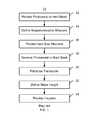
- FIG. 2is a flow chart depicting an exemplary embodiment of a method for fabricating a read sensor using a hybrid mask.
- FIG. 3depicts an ABS view of an exemplary embodiment of a magnetic recording read transducer.
- FIG. 4is a flow chart depicting another exemplary embodiment of a method for fabricating a read sensor using a hybrid mask.
- FIGS. 5-14depict an exemplary embodiment of a magnetic recording transducer during fabrication.
- FIG. 3is an exemplary embodiment of a method 100 for providing magnetic recording transducer. For simplicity, some steps may be omitted.
- the method 100is also described in the context of providing a single recording transducer. However, the method 100 may be used to fabricate multiple transducers at substantially the same time.
- the method 100is also described in the context of particular layers. A particular layer may include multiple materials and/or multiple sub-layers.
- the method 100also may start after formation of other portions of the magnetic recording transducer. For example, the method 100 may start after layers underlying the magnetoresistive sensor, such as a TMR sensor have been fabricated.
- the magnetoresistive layersmay include a pinning layer, a pinned layer, a nonmagnetic spacer layer, and a free layer.
- seed and/or capping layersmay be used.
- the pinning layermay be an AFM or other layer configured to fix, or pin, the magnetization of the pinned layer.
- the pinned layermay be a synthetic antiferromagnetic (SAF) layer including magnetically coupled ferromagnetic layers separated by a nonmagnetic layer.
- SAFsynthetic antiferromagnetic
- the ferromagnetic layersmay be termed pinned and reference sub-layers.
- the nonmagnetic spacer layermay be a conductive layer for a giant magnetoresistive structure, an insulator for a TMR structure, or may have another structure.
- the free layeris ferromagnetic and has a magnetization that is free to change in response to an external magnetic field, for example from a media.
- the free layermay have multiple sub-layers, as may the pinned and reference sub-layers.
- a capping layermay also be provided on the read sensor stack.
- the transducermay be considered to have a sensor region, in which the magnetoresistive structure is to be formed, and a field region distal from the magnetoresistive structure.
- a hybrid maskis provided on the read sensor stack, via step 104 .
- the hybrid maskincludes a hard mask and a field mask.
- the hard maskincludes sensor portion and a field portion.
- the sensor portion of the hard maskcovers the sensor region of read sensor stack.
- the field portion of the hard maskcovers the field region of the read sensor stack.
- the hard maskexposes a of the read sensor stack between the sensor and field portions of the hard mask.
- the field maskcovers the field portion of the hard mask.
- the field maskexposes the sensor portion of the hard mask that is on the sensor region and a portion of the read sensor stack between the sensor region and the field region.
- the portion of the read sensor stack exposed by the hard maskis the same as that which is exposed by the field mask.
- the portions of the read sensor stack exposed by the hard mask and field maskdiffer.
- the hard maskis formed of one or more of SiC, aluminum oxide, amorphous carbon, Ta, and tantalum oxide.
- the field maskis formed from photoresist or an analogous material.
- the field maskhas a sufficient thickness for the hard mask RIE, read read sensor milling, and lift off.
- the thickness of a photoresist field maskmay be approximately one micron or more in some embodiments.
- providing the hybrid maskincludes depositing a hard mask layer and providing a first mask on the hard mask layer. A first portion of the first mask covers the sensor portion of the hard mask.
- a second portion of the first maskcovers at least a portion of the field portion of the hard mask.
- the first maskmay include a bottom antireflective coating layer, such as an AR3 layer and a photoresist layer on the AR3 layer.
- the pattern of the first maskis transferred to the hard mask layer, forming the hard mask.
- another layeris provided on the hard mask layer.
- this layeris a Cr layer.
- the pattern of the first maskis transferred to the additional layer.
- a photoresist layermay then be provided on the hard mask. The photoresist layer is then pattern to form the field mask that covers the field region, but exposes the sensor region.
- the pattern of the field mask plus the portion of the first mask in the sensor regionare transferred to the hard mask.
- the portion of the underlying read sensor stack between the sensor region and the field region exposed by the hard mask and the field maskis the same.
- the hard maskcovers the sensor region, while the field mask typically does not.
- the read sensoris defined from the read sensor stack in the track width direction, via step 106 .
- the exposed portion of the read sensor stackis thus removed.
- Step 106may include performing an ion mill.
- the read sensormay be a TMR junction, a GMR junction, or other sensor.
- the read sensorhas junction angles at its base in the track width direction and a track width. In some embodiments, the track width is less than thirty nanometers.
- At least one hard bias layer for a hard bias structureis deposited, via step 108 .
- Hard bias material(s)include those materials having a sufficiently high coercivity that normal operation of the magnetoresistive structure does not alter the magnetization (and thus the bias) of the hard bias materials.
- a portion of the hard bias material(s)is substantially adjacent to the magnetoresistive structure in the track width direction.
- An insulating layermay be deposited prior to the hard bias materials.
- seed and/or capping layersmay also be provided in step 108 . The seed and/or capping layer(s) may each include sub-layers.
- sealingis accomplished by depositing one or more layers.
- sealing the hard bias layer(s)may include depositing a bilayer including a Ta sub-layer and a Ru sub-layer on the Ta sub-layer.
- the step of sealing the hard bias layer(s)may include depositing a trilayer including a Ru sub-layer sandwiched by two Ta sub-layers.
- Step 112The field mask is lifted off, via step 112 .
- the transduceris planarized, via step 114 .
- Step 114may include performing a CMP. In other embodiments, other mechanisms may be used to planarize the transducer.
- a portion of the hard bias structure as well as the hard maskis removed.
- the hard biasmay thus be removed from the region on top of the read sensor.
- a remaining portion of the hard maskis removed after the transducer is planarized. For example, an RIE appropriate for the hard mask maybe performed. Because the hard mask may be thinned in the planarization of step 114 , removal of the hard mask may be facilitated. Fabrication of the transducer may then be completed. For example, the stripe height (length perpendicular to the ABS) for the read sensor may be defined. A nonmagnetic gap, shields, and other structures may also be formed.
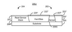
- FIG. 3depicts the transducer 130 after the method 100 is completed. For clarity, FIG. 3 is not to scale. In addition, only a portion of the transducer 130 is shown. The transducer is also described in the context of particular layers and structures. However, sublayers and/or substructures may also be provided.
- the read sensor stackis a TMR stack and has been so labeled.
- the read transducer 130includes a magnetoresistive sensor 132 S, remaining TMR stack 132 F, insulating layer 134 , hard bias structures 136 on underlying layers 131 . Thus, the underlying layers 131 may be termed a substrate.
- the transducer 130includes field regions 138 and sensor region 140 in which the TMR sensor 132 S resides. Because they are in the field regions 138 , the remaining portions of the read sensor stack are labeled 132 F.
- the transducer 130 having a magnetoresistive read sensor 132may be formed. Because a hard mask is used in the sensor region 140 without a photoresist mask on this region 140 , a read sensor 132 S having the desired small track width may be fabricated. Because a field mask that can be lifted off or removed in some analogous, simple fashion, the hard bias material(s) may be more easily removed from the larger field regions 138 . Damage to the underlying layers 132 F and/or 136 may thus be reduced or avoided. Because the hard bias layer(s) 136 are sealed, oxidation and/or other issues with the hard bias layer(s) 136 may be mitigated or prevented.
- planarizing the transducer, and the attendant thinning of the hard maskmay reduce stresses due to the hard mask. This may limit or prevent delamination of the TMR sensor 132 S during removal of the hard mask. Thus, the fabrication of the transducer 130 may be improved.
- FIG. 4is a flow chart depicting another exemplary embodiment of a method 150 for fabricating a magnetic recording transducer.
- FIGS. 5-14depict ABS views of another exemplary embodiment of a magnetic recording transducer 200 during fabrication. Because the transducer 200 is being formed in FIGS. 5-13 , the transducer 200 is denoted as transducer 200 A, 200 B, 200 C, 200 D, 200 E, 200 F, 200 G, 200 H, 200 I and 200 J in FIGS. 5 , 6 , 7 , 8 , 9 , 10 , 11 , 12 , 13 and 14 , respectively. However, the transducer is simply referred to as the transducer 200 in the text. For clarity, FIGS. 5-14 are not to scale.
- the method 150is described in the context of the transducer 200 . For simplicity, some steps of the method 150 may be omitted. The method 150 is also described in the context of providing a single recording transducer 200 . However, the method 150 may be used to fabricate multiple transducers at substantially the same time. The method 150 and transducer 200 are also described in the context of particular layers. A particular layer may include multiple materials and/or multiple sub-layers. The method 150 also may start after formation of other portions of the magnetic recording transducer 200 . Further, the transducer may be considered to have a device region, in which the magnetoresistive structure is to be formed, and a field region distal from the magnetoresistive structure.
- the magnetoresistive layersmay include a pinning layer, a pinned layer, a nonmagnetic spacer layer, and a free layer.
- seed and/or capping layersmay be used. Examples of such layers are described above.
- a hard mask layeris provided on the read sensor stack, via step 154 .
- Step 154includes blanket depositing a hard mask layer such as SiC, amorphous carbon (e.g. sputtered carbon), aluminum oxide, Ta, and/or tantalum oxide on the read sensor stack.
- a hard mask layersuch as SiC, amorphous carbon (e.g. sputtered carbon), aluminum oxide, Ta, and/or tantalum oxide
- the step 154includes depositing a hard mask layer having a thickness of not more than seventy nanometers.
- the hard mask layer provided in step 154has a thickness of not more than sixty nanometers. However, in other embodiments, other thicknesses of the hard mask layer may be used.
- a Cr layeris deposited on the hard mask layer, via step 156 .
- another layermay be used.
- a first maskis provided, via step 158 .
- the first maskmay include a BARC layer and a photoresist layer on the BARC layer.
- the first maskhas a pattern that includes a first portion covering a sensor portion of the hard mask layer and a second portion covering at least a portion of the field region.
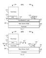
- FIG. 5depicts an ABS view of the transducer 200 after the exposed portion of the Cr is removed in step 160 .
- a sensor portion 202 and a field portion 204 of the transducer 204are shown.
- the transducer 200also includes a read sensor stack 206 on underlying layer(s) indicated as a substrate 205 .
- the substrate 205may include underlying layers such as shield or insulating gap layers.
- a capping layer 207 for the read sensor stack 206 and a hard mask layer 208are also shown.
- the hard mask layer 208is shown as being blanket deposited on the read sensor stack 206 .
- a Cr layer 210 that has been patternedis also shown.
- the first mask 211is included.
- the first mask 211includes an AR3 layer 212 and a photoresist layer 214 .
- the AR3 layeracts as a BARC layer for the photoresist layer 214 .
- the first mask 211covers part of the field region 204 and the sensor region 202 .
- FIG. 6depicts the transducer 200 after the photoresist mask 214 is removed after the exposed portion of the Cr is removed.
- the AR3 layer 212 ′remains from the first mask 211 .
- FIG. 7depicts the transducer 200 after step 164 is performed.
- the field mask 216is shown. In the embodiment shown, the field mask 216 extends beyond the first mask/BARC layer 212 ′. However, in other embodiments, the field mask 216 may extend only to the edge of the first mask/BARC layer 212 ′.
- the pattern of the field mask 216 and remaining exposed portion of the first mask—the BARC layers 212 ′ and Cr layer 210 ′ in the sensor region 202is transferred to the hard mask 208 , via step 166 .
- the exposed portion of the hard mask 208 between the field mask 216 and BARC layer 212 ′/Cr 210 ′ in the sensor region 202is removed.
- FIG. 8depicts the transducer 200 after step 166 is performed.
- a portion of the hard mask layer 208has been removed, hard mask 208 ′.
- the hard mask 208 ′includes portions 208 S and 208 F in the sensor region 202 and the field region 204 , respectively.
- the hard mask 208 ′ and the field mask 216together form hybrid mask 218 .
- any remaining portion of the first mask 211such as the BARC 212 ′ as well as the Cr layer 210 ′ may be considered part of the hybrid mask.
- the read sensoris defined from the read sensor stack 206 in a track width direction, via step 168 .
- the read sensormay also be defined in the stripe height direction.
- Step 168may include performing an ion mill. Thus, a portion of the read sensor stack 206 between the sensor region 202 and the field region 204 is removed. Also in step 168 any remaining portion of the first photoresist layer 214 (shown in FIG. 5 only) on the sensor region 202 is consumed. In the embodiment shown, the first photoresist layer 214 is consumed previously.
- FIG. 9depicts the transducer 200 after step 168 is performed. Thus, the sensor 206 S has been formed.
- the track width of the sensor 206 Smay be small, including in the sub-thirty micron range.
- a portion of the read sensor stack 206 F covered by the field mask 216 and portion 208 F of the hard mask 208 Fremains in the field 204 .
- One or more hard bias layersare deposited, via step 170 .
- the hard bias layer(s)are blanket deposited.
- FIG. 10depicts the transducer 200 after step 170 is performed. A portion of the hard bias layer(s) are on the field mask 216 of the hybrid mask 218 , a portion of the hard bias layer(s) would be between the field region 204 and the sensor region 202 , and a portion of the hard bias layer(s) would be on the sensor region 202 .
- a first Ta layeris deposited, via step 172 .
- a Ru layeris deposited on the first Ta layer, via step 174 .
- a second Ta layeris deposited on the Ru layer, via step 176 .
- the three layersform a sealing layer.
- other layer(s)may be deposited to seal the hard bias layers.
- FIG. 10depicts the transducer 100 after step 178 is performed.
- hard bias layer(s) 220are shown.
- a sealing layer 222that would include the Ta/Ru/Ta trilayer is also depicted.
- Sacrificial aluminum oxide layer 224that covers the portion of the transducer 200 depicted.
- the sacrificial layermay be thinner on the sidewalls of the hybrid mask 218 due to the shadowing effect.
- the field mask 216is lifted off, via step 180 .
- the BARC layer 212 ′is removed from the field region 204 , via step 182 .
- FIG. 11depicts the transducer 200 after step 182 is performed.
- the field mask 216 and BARC 214 ′have been removed.
- Portions of the hard bias 220 , sealing layer(s) 222 , and sacrificial aluminum oxide layer 224 on the field mask 216have been removed.
- only hard bias layer(s) 220 ′, sealing layer(s) 222 ′, and sacrificial layer 224 ′remain.
- a remaining portion of the Cr layer 210 ′is removed, via step 184 .
- a portion of the hard mask 208 ′is also removed.
- the portion of the hard bias layer(s) 220 ′may be removed.
- FIG. 12depicts the transducer 200 after step 184 is performed.
- the Cr layer 210has been removed.
- the hard mask 208 ′′remains, but has been thinned. More specifically, the hard mask 208 S′ and 208 F′ have been thinned. The may reduce the stress in the hard mask 208 F′ and 208 S′. Thus, delamination of the sensor stack 206 F and the sensor 206 S in subsequent steps may be reduced.
- adjusting of the thickness of the sacrificial layer 224 ′may allow the hard mask thickness 208 F′ and 208 S′ to be thinned to the desired thickness in step 184 .
- the process margins for a subsequent planarizationmay be improved.
- step 186includes performing a CMP.
- FIG. 13depicts the transducer 200 after step 186 is performed. In the embodiment shown, a portion of the hard mask 208 F′′ in the field region remains. However, in another embodiment, the hard mask 208 ′′ may be completely removed. Thus, in some embodiments, any hard mask 208 ′′ remaining is optionally removed, via step 188 .
- FIG. 14depicts the transducer 200 after step 186 or 188 has been performed. Thus, the hard mask 208 ′′ has been completely removed. Fabrication of the transducer 200 may then be completed. Using the method 150 , the transducer 200 having a magnetoresistive read sensor 206 S may be formed.
- the hybrid mask 218may facilitate fabrication of the transducer. Because the hard mask 208 S of the hybrid mask 218 is used in the sensor region 202 without a photoresist mask on this region 202 , a read sensor 206 S having the desired small track width may be fabricated. Because a field mask 216 that can be lifted off or removed in some analogous, simple fashion, the hard bias material(s) 220 may be more easily removed from the larger field regions 204 . Damage to the underlying layers 2206 F and 206 S may thus be reduced or avoided. Because the hard bias layer(s) 220 are sealed using sealing layer(s) 222 , oxidation and/or other issues with the hard bias layer(s) 220 may be mitigated or prevented.
- planarizing the transducer, and the attendant thinning of the hard mask 208 ′′′,may reduce stresses due to the hard mask 208 ′′. This may limit or prevent delamination of the TMR stack 206 F and 206 S Thus, the fabrication of the transducer 200 may be improved.
Landscapes
- Engineering & Computer Science (AREA)
- Manufacturing & Machinery (AREA)
- Physics & Mathematics (AREA)
- Condensed Matter Physics & Semiconductors (AREA)
- General Physics & Mathematics (AREA)
- Magnetic Heads (AREA)
Abstract
Description
Claims (11)
Priority Applications (1)
| Application Number | Priority Date | Filing Date | Title |
|---|---|---|---|
| US13/309,357US8607438B1 (en) | 2011-12-01 | 2011-12-01 | Method for fabricating a read sensor for a read transducer |
Applications Claiming Priority (1)
| Application Number | Priority Date | Filing Date | Title |
|---|---|---|---|
| US13/309,357US8607438B1 (en) | 2011-12-01 | 2011-12-01 | Method for fabricating a read sensor for a read transducer |
Publications (1)
| Publication Number | Publication Date |
|---|---|
| US8607438B1true US8607438B1 (en) | 2013-12-17 |
Family
ID=49725578
Family Applications (1)
| Application Number | Title | Priority Date | Filing Date |
|---|---|---|---|
| US13/309,357Expired - Fee RelatedUS8607438B1 (en) | 2011-12-01 | 2011-12-01 | Method for fabricating a read sensor for a read transducer |
Country Status (1)
| Country | Link |
|---|---|
| US (1) | US8607438B1 (en) |
Cited By (131)
| Publication number | Priority date | Publication date | Assignee | Title |
|---|---|---|---|---|
| US8790524B1 (en) | 2010-09-13 | 2014-07-29 | Western Digital (Fremont), Llc | Method and system for providing a magnetic recording transducer using a line hard mask and a wet-etchable mask |
| US8830628B1 (en) | 2009-02-23 | 2014-09-09 | Western Digital (Fremont), Llc | Method and system for providing a perpendicular magnetic recording head |
| US8879207B1 (en) | 2011-12-20 | 2014-11-04 | Western Digital (Fremont), Llc | Method for providing a side shield for a magnetic recording transducer using an air bridge |
| US8883017B1 (en) | 2013-03-12 | 2014-11-11 | Western Digital (Fremont), Llc | Method and system for providing a read transducer having seamless interfaces |
| US8917581B1 (en) | 2013-12-18 | 2014-12-23 | Western Digital Technologies, Inc. | Self-anneal process for a near field transducer and chimney in a hard disk drive assembly |
| US8923102B1 (en) | 2013-07-16 | 2014-12-30 | Western Digital (Fremont), Llc | Optical grating coupling for interferometric waveguides in heat assisted magnetic recording heads |
| US8947985B1 (en) | 2013-07-16 | 2015-02-03 | Western Digital (Fremont), Llc | Heat assisted magnetic recording transducers having a recessed pole |
| US8953422B1 (en) | 2014-06-10 | 2015-02-10 | Western Digital (Fremont), Llc | Near field transducer using dielectric waveguide core with fine ridge feature |
| US8958272B1 (en) | 2014-06-10 | 2015-02-17 | Western Digital (Fremont), Llc | Interfering near field transducer for energy assisted magnetic recording |
| US8971160B1 (en) | 2013-12-19 | 2015-03-03 | Western Digital (Fremont), Llc | Near field transducer with high refractive index pin for heat assisted magnetic recording |
| US8970988B1 (en) | 2013-12-31 | 2015-03-03 | Western Digital (Fremont), Llc | Electric gaps and method for making electric gaps for multiple sensor arrays |
| US8976635B1 (en) | 2014-06-10 | 2015-03-10 | Western Digital (Fremont), Llc | Near field transducer driven by a transverse electric waveguide for energy assisted magnetic recording |
| US8982508B1 (en) | 2011-10-31 | 2015-03-17 | Western Digital (Fremont), Llc | Method for providing a side shield for a magnetic recording transducer |
| US8980109B1 (en) | 2012-12-11 | 2015-03-17 | Western Digital (Fremont), Llc | Method for providing a magnetic recording transducer using a combined main pole and side shield CMP for a wraparound shield scheme |
| US8984740B1 (en) | 2012-11-30 | 2015-03-24 | Western Digital (Fremont), Llc | Process for providing a magnetic recording transducer having a smooth magnetic seed layer |
| US8988825B1 (en) | 2014-02-28 | 2015-03-24 | Western Digital (Fremont, LLC | Method for fabricating a magnetic writer having half-side shields |
| US8988812B1 (en) | 2013-11-27 | 2015-03-24 | Western Digital (Fremont), Llc | Multi-sensor array configuration for a two-dimensional magnetic recording (TDMR) operation |
| US8993217B1 (en) | 2013-04-04 | 2015-03-31 | Western Digital (Fremont), Llc | Double exposure technique for high resolution disk imaging |
| US8995087B1 (en) | 2006-11-29 | 2015-03-31 | Western Digital (Fremont), Llc | Perpendicular magnetic recording write head having a wrap around shield |
| US9001467B1 (en) | 2014-03-05 | 2015-04-07 | Western Digital (Fremont), Llc | Method for fabricating side shields in a magnetic writer |
| US9001628B1 (en) | 2013-12-16 | 2015-04-07 | Western Digital (Fremont), Llc | Assistant waveguides for evaluating main waveguide coupling efficiency and diode laser alignment tolerances for hard disk |
| US8997832B1 (en) | 2010-11-23 | 2015-04-07 | Western Digital (Fremont), Llc | Method of fabricating micrometer scale components |
| US9007879B1 (en) | 2014-06-10 | 2015-04-14 | Western Digital (Fremont), Llc | Interfering near field transducer having a wide metal bar feature for energy assisted magnetic recording |
| US9007725B1 (en) | 2014-10-07 | 2015-04-14 | Western Digital (Fremont), Llc | Sensor with positive coupling between dual ferromagnetic free layer laminates |
| US9007719B1 (en) | 2013-10-23 | 2015-04-14 | Western Digital (Fremont), Llc | Systems and methods for using double mask techniques to achieve very small features |
| US9013836B1 (en) | 2013-04-02 | 2015-04-21 | Western Digital (Fremont), Llc | Method and system for providing an antiferromagnetically coupled return pole |
| US9042051B2 (en) | 2013-08-15 | 2015-05-26 | Western Digital (Fremont), Llc | Gradient write gap for perpendicular magnetic recording writer |
| US9042057B1 (en) | 2013-01-09 | 2015-05-26 | Western Digital (Fremont), Llc | Methods for providing magnetic storage elements with high magneto-resistance using Heusler alloys |
| US9042208B1 (en) | 2013-03-11 | 2015-05-26 | Western Digital Technologies, Inc. | Disk drive measuring fly height by applying a bias voltage to an electrically insulated write component of a head |
| US9042052B1 (en) | 2014-06-23 | 2015-05-26 | Western Digital (Fremont), Llc | Magnetic writer having a partially shunted coil |
| US9042058B1 (en) | 2013-10-17 | 2015-05-26 | Western Digital Technologies, Inc. | Shield designed for middle shields in a multiple sensor array |
| US9053735B1 (en) | 2014-06-20 | 2015-06-09 | Western Digital (Fremont), Llc | Method for fabricating a magnetic writer using a full-film metal planarization |
| US9065043B1 (en) | 2012-06-29 | 2015-06-23 | Western Digital (Fremont), Llc | Tunnel magnetoresistance read head with narrow shield-to-shield spacing |
| US9064527B1 (en) | 2013-04-12 | 2015-06-23 | Western Digital (Fremont), Llc | High order tapered waveguide for use in a heat assisted magnetic recording head |
| US9064528B1 (en) | 2013-05-17 | 2015-06-23 | Western Digital Technologies, Inc. | Interferometric waveguide usable in shingled heat assisted magnetic recording in the absence of a near-field transducer |
| US9064507B1 (en) | 2009-07-31 | 2015-06-23 | Western Digital (Fremont), Llc | Magnetic etch-stop layer for magnetoresistive read heads |
| US9070381B1 (en) | 2013-04-12 | 2015-06-30 | Western Digital (Fremont), Llc | Magnetic recording read transducer having a laminated free layer |
| US9082423B1 (en) | 2013-12-18 | 2015-07-14 | Western Digital (Fremont), Llc | Magnetic recording write transducer having an improved trailing surface profile |
| US9087527B1 (en) | 2014-10-28 | 2015-07-21 | Western Digital (Fremont), Llc | Apparatus and method for middle shield connection in magnetic recording transducers |
| US9087534B1 (en) | 2011-12-20 | 2015-07-21 | Western Digital (Fremont), Llc | Method and system for providing a read transducer having soft and hard magnetic bias structures |
| US9093639B2 (en) | 2012-02-21 | 2015-07-28 | Western Digital (Fremont), Llc | Methods for manufacturing a magnetoresistive structure utilizing heating and cooling |
| US9104107B1 (en) | 2013-04-03 | 2015-08-11 | Western Digital (Fremont), Llc | DUV photoresist process |
| US9111564B1 (en) | 2013-04-02 | 2015-08-18 | Western Digital (Fremont), Llc | Magnetic recording writer having a main pole with multiple flare angles |
| US9111558B1 (en) | 2014-03-14 | 2015-08-18 | Western Digital (Fremont), Llc | System and method of diffractive focusing of light in a waveguide |
| US9111550B1 (en) | 2014-12-04 | 2015-08-18 | Western Digital (Fremont), Llc | Write transducer having a magnetic buffer layer spaced between a side shield and a write pole by non-magnetic layers |
| US9123362B1 (en) | 2011-03-22 | 2015-09-01 | Western Digital (Fremont), Llc | Methods for assembling an electrically assisted magnetic recording (EAMR) head |
| US9123358B1 (en) | 2012-06-11 | 2015-09-01 | Western Digital (Fremont), Llc | Conformal high moment side shield seed layer for perpendicular magnetic recording writer |
| US9123359B1 (en) | 2010-12-22 | 2015-09-01 | Western Digital (Fremont), Llc | Magnetic recording transducer with sputtered antiferromagnetic coupling trilayer between plated ferromagnetic shields and method of fabrication |
| US9123374B1 (en) | 2015-02-12 | 2015-09-01 | Western Digital (Fremont), Llc | Heat assisted magnetic recording writer having an integrated polarization rotation plate |
| US9135937B1 (en) | 2014-05-09 | 2015-09-15 | Western Digital (Fremont), Llc | Current modulation on laser diode for energy assisted magnetic recording transducer |
| US9135930B1 (en) | 2014-03-06 | 2015-09-15 | Western Digital (Fremont), Llc | Method for fabricating a magnetic write pole using vacuum deposition |
| US9142233B1 (en) | 2014-02-28 | 2015-09-22 | Western Digital (Fremont), Llc | Heat assisted magnetic recording writer having a recessed pole |
| US9147404B1 (en) | 2015-03-31 | 2015-09-29 | Western Digital (Fremont), Llc | Method and system for providing a read transducer having a dual free layer |
| US9147408B1 (en) | 2013-12-19 | 2015-09-29 | Western Digital (Fremont), Llc | Heated AFM layer deposition and cooling process for TMR magnetic recording sensor with high pinning field |
| US9153255B1 (en) | 2014-03-05 | 2015-10-06 | Western Digital (Fremont), Llc | Method for fabricating a magnetic writer having an asymmetric gap and shields |
| US9183854B2 (en) | 2014-02-24 | 2015-11-10 | Western Digital (Fremont), Llc | Method to make interferometric taper waveguide for HAMR light delivery |
| US9190085B1 (en) | 2014-03-12 | 2015-11-17 | Western Digital (Fremont), Llc | Waveguide with reflective grating for localized energy intensity |
| US9190079B1 (en) | 2014-09-22 | 2015-11-17 | Western Digital (Fremont), Llc | Magnetic write pole having engineered radius of curvature and chisel angle profiles |
| US9194692B1 (en) | 2013-12-06 | 2015-11-24 | Western Digital (Fremont), Llc | Systems and methods for using white light interferometry to measure undercut of a bi-layer structure |
| US9202480B2 (en) | 2009-10-14 | 2015-12-01 | Western Digital (Fremont), LLC. | Double patterning hard mask for damascene perpendicular magnetic recording (PMR) writer |
| US9202493B1 (en) | 2014-02-28 | 2015-12-01 | Western Digital (Fremont), Llc | Method of making an ultra-sharp tip mode converter for a HAMR head |
| US9214169B1 (en) | 2014-06-20 | 2015-12-15 | Western Digital (Fremont), Llc | Magnetic recording read transducer having a laminated free layer |
| US9214165B1 (en) | 2014-12-18 | 2015-12-15 | Western Digital (Fremont), Llc | Magnetic writer having a gradient in saturation magnetization of the shields |
| US9214172B2 (en) | 2013-10-23 | 2015-12-15 | Western Digital (Fremont), Llc | Method of manufacturing a magnetic read head |
| US9213322B1 (en) | 2012-08-16 | 2015-12-15 | Western Digital (Fremont), Llc | Methods for providing run to run process control using a dynamic tuner |
| US9230565B1 (en) | 2014-06-24 | 2016-01-05 | Western Digital (Fremont), Llc | Magnetic shield for magnetic recording head |
| US9236560B1 (en) | 2014-12-08 | 2016-01-12 | Western Digital (Fremont), Llc | Spin transfer torque tunneling magnetoresistive device having a laminated free layer with perpendicular magnetic anisotropy |
| US9245562B1 (en) | 2015-03-30 | 2016-01-26 | Western Digital (Fremont), Llc | Magnetic recording writer with a composite main pole |
| US9245545B1 (en) | 2013-04-12 | 2016-01-26 | Wester Digital (Fremont), Llc | Short yoke length coils for magnetic heads in disk drives |
| US9245543B1 (en) | 2010-06-25 | 2016-01-26 | Western Digital (Fremont), Llc | Method for providing an energy assisted magnetic recording head having a laser integrally mounted to the slider |
| US9251813B1 (en) | 2009-04-19 | 2016-02-02 | Western Digital (Fremont), Llc | Method of making a magnetic recording head |
| US9263071B1 (en) | 2015-03-31 | 2016-02-16 | Western Digital (Fremont), Llc | Flat NFT for heat assisted magnetic recording |
| US9263067B1 (en) | 2013-05-29 | 2016-02-16 | Western Digital (Fremont), Llc | Process for making PMR writer with constant side wall angle |
| US9269382B1 (en) | 2012-06-29 | 2016-02-23 | Western Digital (Fremont), Llc | Method and system for providing a read transducer having improved pinning of the pinned layer at higher recording densities |
| US9275657B1 (en) | 2013-08-14 | 2016-03-01 | Western Digital (Fremont), Llc | Process for making PMR writer with non-conformal side gaps |
| US9280990B1 (en) | 2013-12-11 | 2016-03-08 | Western Digital (Fremont), Llc | Method for fabricating a magnetic writer using multiple etches |
| US9286919B1 (en) | 2014-12-17 | 2016-03-15 | Western Digital (Fremont), Llc | Magnetic writer having a dual side gap |
| US9287494B1 (en) | 2013-06-28 | 2016-03-15 | Western Digital (Fremont), Llc | Magnetic tunnel junction (MTJ) with a magnesium oxide tunnel barrier |
| US9305583B1 (en) | 2014-02-18 | 2016-04-05 | Western Digital (Fremont), Llc | Method for fabricating a magnetic writer using multiple etches of damascene materials |
| US9312064B1 (en) | 2015-03-02 | 2016-04-12 | Western Digital (Fremont), Llc | Method to fabricate a magnetic head including ion milling of read gap using dual layer hard mask |
| US9318130B1 (en) | 2013-07-02 | 2016-04-19 | Western Digital (Fremont), Llc | Method to fabricate tunneling magnetic recording heads with extended pinned layer |
| US9336814B1 (en) | 2013-03-12 | 2016-05-10 | Western Digital (Fremont), Llc | Inverse tapered waveguide for use in a heat assisted magnetic recording head |
| US9343098B1 (en) | 2013-08-23 | 2016-05-17 | Western Digital (Fremont), Llc | Method for providing a heat assisted magnetic recording transducer having protective pads |
| US9343087B1 (en) | 2014-12-21 | 2016-05-17 | Western Digital (Fremont), Llc | Method for fabricating a magnetic writer having half shields |
| US9343086B1 (en) | 2013-09-11 | 2016-05-17 | Western Digital (Fremont), Llc | Magnetic recording write transducer having an improved sidewall angle profile |
| US9349392B1 (en) | 2012-05-24 | 2016-05-24 | Western Digital (Fremont), Llc | Methods for improving adhesion on dielectric substrates |
| US9349394B1 (en) | 2013-10-18 | 2016-05-24 | Western Digital (Fremont), Llc | Method for fabricating a magnetic writer having a gradient side gap |
| US9361913B1 (en) | 2013-06-03 | 2016-06-07 | Western Digital (Fremont), Llc | Recording read heads with a multi-layer AFM layer methods and apparatuses |
| US9361914B1 (en) | 2014-06-18 | 2016-06-07 | Western Digital (Fremont), Llc | Magnetic sensor with thin capping layer |
| US9368134B1 (en) | 2010-12-16 | 2016-06-14 | Western Digital (Fremont), Llc | Method and system for providing an antiferromagnetically coupled writer |
| US9384763B1 (en) | 2015-03-26 | 2016-07-05 | Western Digital (Fremont), Llc | Dual free layer magnetic reader having a rear bias structure including a soft bias layer |
| US9384765B1 (en) | 2015-09-24 | 2016-07-05 | Western Digital (Fremont), Llc | Method and system for providing a HAMR writer having improved optical efficiency |
| US9396742B1 (en) | 2012-11-30 | 2016-07-19 | Western Digital (Fremont), Llc | Magnetoresistive sensor for a magnetic storage system read head, and fabrication method thereof |
| US9396743B1 (en) | 2014-02-28 | 2016-07-19 | Western Digital (Fremont), Llc | Systems and methods for controlling soft bias thickness for tunnel magnetoresistance readers |
| US9406331B1 (en) | 2013-06-17 | 2016-08-02 | Western Digital (Fremont), Llc | Method for making ultra-narrow read sensor and read transducer device resulting therefrom |
| US9424866B1 (en) | 2015-09-24 | 2016-08-23 | Western Digital (Fremont), Llc | Heat assisted magnetic recording write apparatus having a dielectric gap |
| US9431047B1 (en) | 2013-05-01 | 2016-08-30 | Western Digital (Fremont), Llc | Method for providing an improved AFM reader shield |
| US9431039B1 (en) | 2013-05-21 | 2016-08-30 | Western Digital (Fremont), Llc | Multiple sensor array usable in two-dimensional magnetic recording |
| US9431031B1 (en) | 2015-03-24 | 2016-08-30 | Western Digital (Fremont), Llc | System and method for magnetic transducers having multiple sensors and AFC shields |
| US9431038B1 (en) | 2015-06-29 | 2016-08-30 | Western Digital (Fremont), Llc | Method for fabricating a magnetic write pole having an improved sidewall angle profile |
| US9431032B1 (en) | 2013-08-14 | 2016-08-30 | Western Digital (Fremont), Llc | Electrical connection arrangement for a multiple sensor array usable in two-dimensional magnetic recording |
| US9437251B1 (en) | 2014-12-22 | 2016-09-06 | Western Digital (Fremont), Llc | Apparatus and method having TDMR reader to reader shunts |
| US9441938B1 (en) | 2013-10-08 | 2016-09-13 | Western Digital (Fremont), Llc | Test structures for measuring near field transducer disc length |
| US9443541B1 (en) | 2015-03-24 | 2016-09-13 | Western Digital (Fremont), Llc | Magnetic writer having a gradient in saturation magnetization of the shields and return pole |
| US9449621B1 (en) | 2015-03-26 | 2016-09-20 | Western Digital (Fremont), Llc | Dual free layer magnetic reader having a rear bias structure having a high aspect ratio |
| US9449625B1 (en) | 2014-12-24 | 2016-09-20 | Western Digital (Fremont), Llc | Heat assisted magnetic recording head having a plurality of diffusion barrier layers |
| US9472216B1 (en) | 2015-09-23 | 2016-10-18 | Western Digital (Fremont), Llc | Differential dual free layer magnetic reader |
| US9484051B1 (en) | 2015-11-09 | 2016-11-01 | The Provost, Fellows, Foundation Scholars and the other members of Board, of the College of the Holy and Undivided Trinity of Queen Elizabeth near Dublin | Method and system for reducing undesirable reflections in a HAMR write apparatus |
| US9508365B1 (en) | 2015-06-24 | 2016-11-29 | Western Digital (Fremont), LLC. | Magnetic reader having a crystal decoupling structure |
| US9508363B1 (en) | 2014-06-17 | 2016-11-29 | Western Digital (Fremont), Llc | Method for fabricating a magnetic write pole having a leading edge bevel |
| US9508372B1 (en) | 2015-06-03 | 2016-11-29 | Western Digital (Fremont), Llc | Shingle magnetic writer having a low sidewall angle pole |
| US9530443B1 (en) | 2015-06-25 | 2016-12-27 | Western Digital (Fremont), Llc | Method for fabricating a magnetic recording device having a high aspect ratio structure |
| US9564150B1 (en) | 2015-11-24 | 2017-02-07 | Western Digital (Fremont), Llc | Magnetic read apparatus having an improved read sensor isolation circuit |
| US9595273B1 (en) | 2015-09-30 | 2017-03-14 | Western Digital (Fremont), Llc | Shingle magnetic writer having nonconformal shields |
| US9646639B2 (en) | 2015-06-26 | 2017-05-09 | Western Digital (Fremont), Llc | Heat assisted magnetic recording writer having integrated polarization rotation waveguides |
| US9666214B1 (en) | 2015-09-23 | 2017-05-30 | Western Digital (Fremont), Llc | Free layer magnetic reader that may have a reduced shield-to-shield spacing |
| US9721595B1 (en) | 2014-12-04 | 2017-08-01 | Western Digital (Fremont), Llc | Method for providing a storage device |
| US9741366B1 (en) | 2014-12-18 | 2017-08-22 | Western Digital (Fremont), Llc | Method for fabricating a magnetic writer having a gradient in saturation magnetization of the shields |
| US9740805B1 (en) | 2015-12-01 | 2017-08-22 | Western Digital (Fremont), Llc | Method and system for detecting hotspots for photolithographically-defined devices |
| US9754611B1 (en) | 2015-11-30 | 2017-09-05 | Western Digital (Fremont), Llc | Magnetic recording write apparatus having a stepped conformal trailing shield |
| US9767831B1 (en) | 2015-12-01 | 2017-09-19 | Western Digital (Fremont), Llc | Magnetic writer having convex trailing surface pole and conformal write gap |
| US9786301B1 (en) | 2014-12-02 | 2017-10-10 | Western Digital (Fremont), Llc | Apparatuses and methods for providing thin shields in a multiple sensor array |
| US9799351B1 (en) | 2015-11-30 | 2017-10-24 | Western Digital (Fremont), Llc | Short yoke length writer having assist coils |
| US9812155B1 (en) | 2015-11-23 | 2017-11-07 | Western Digital (Fremont), Llc | Method and system for fabricating high junction angle read sensors |
| US9842615B1 (en) | 2015-06-26 | 2017-12-12 | Western Digital (Fremont), Llc | Magnetic reader having a nonmagnetic insertion layer for the pinning layer |
| US9858951B1 (en) | 2015-12-01 | 2018-01-02 | Western Digital (Fremont), Llc | Method for providing a multilayer AFM layer in a read sensor |
| US9881638B1 (en) | 2014-12-17 | 2018-01-30 | Western Digital (Fremont), Llc | Method for providing a near-field transducer (NFT) for a heat assisted magnetic recording (HAMR) device |
| US9934811B1 (en) | 2014-03-07 | 2018-04-03 | Western Digital (Fremont), Llc | Methods for controlling stray fields of magnetic features using magneto-elastic anisotropy |
| US9953670B1 (en) | 2015-11-10 | 2018-04-24 | Western Digital (Fremont), Llc | Method and system for providing a HAMR writer including a multi-mode interference device |
| US10037770B1 (en) | 2015-11-12 | 2018-07-31 | Western Digital (Fremont), Llc | Method for providing a magnetic recording write apparatus having a seamless pole |
| US10074387B1 (en) | 2014-12-21 | 2018-09-11 | Western Digital (Fremont), Llc | Method and system for providing a read transducer having symmetric antiferromagnetically coupled shields |
Citations (40)
| Publication number | Priority date | Publication date | Assignee | Title |
|---|---|---|---|---|
| US5438747A (en) | 1994-03-09 | 1995-08-08 | International Business Machines Corporation | Method of making a thin film merged MR head with aligned pole tips |
| US5867890A (en) | 1997-12-17 | 1999-02-09 | International Business Machines Corporation | Method for making a thin film merged magnetoresistive read/inductive write head having a pedestal pole tip |
| US5874010A (en) | 1996-07-17 | 1999-02-23 | Headway Technologies, Inc. | Pole trimming technique for high data rate thin film heads |
| US6043960A (en) | 1997-12-22 | 2000-03-28 | International Business Machines Corporation | Inverted merged MR head with track width defining first pole tip component constructed on a side wall |
| US20010001256A1 (en)* | 1998-08-24 | 2001-05-17 | Richard Hsiao | Read sensor with self-aligned low resistance leads and method of making |
| US6472107B1 (en) | 1999-09-30 | 2002-10-29 | Photronics, Inc. | Disposable hard mask for photomask plasma etching |
| US6692898B2 (en) | 2001-01-24 | 2004-02-17 | Infineon Technologies Ag | Self-aligned conductive line for cross-point magnetic memory integrated circuits |
| US6729014B2 (en) | 2001-04-23 | 2004-05-04 | Headway Technologies, Inc. | Magnetic assist read track-width definition for a lead overlay top spin-valve GMR head |
| US6737281B1 (en) | 2002-01-08 | 2004-05-18 | Western Digital (Fremont), Inc. | Method of making transducer with inorganic nonferromagnetic apex region |
| US20040229430A1 (en) | 2003-05-14 | 2004-11-18 | Frank Findeis | Fabrication process for a magnetic tunnel junction device |
| US20050024779A1 (en) | 2003-07-30 | 2005-02-03 | Hitachi Global Storage Technologies, Inc. | Method of making a perpendicular recording magnetic head pole tip with an etchable adhesion CMP stop layer |
| US6861177B2 (en) | 2002-02-21 | 2005-03-01 | Hitachi Global Storage Technologies Netherlands B.V. | Method of forming a read sensor using a lift-off mask having a hardmask layer and a release layer |
| US6862798B2 (en) | 2002-01-18 | 2005-03-08 | Hitachi Global Storage Technologies Netherlands B.V. | Method of making a narrow pole tip by ion beam deposition |
| US6872467B2 (en) | 2002-11-12 | 2005-03-29 | Nve Corporation | Magnetic field sensor with augmented magnetoresistive sensing layer |
| US20050066517A1 (en) | 2003-09-30 | 2005-03-31 | Bedell Daniel Wayne | Ion mill process with sacrificial mask layer to fabricate pole tip for perpendicular recording |
| US20050117251A1 (en) | 2003-11-28 | 2005-06-02 | Tdk Corporation | Thin film magnetic head, method of manufacturing the same, and magnetic recording apparatus |
| US20050185332A1 (en) | 2004-02-23 | 2005-08-25 | Hitachi Global Storage Technologies | Perpendicular pole structure and method of fabricating the same |
| US20050241140A1 (en) | 2004-04-30 | 2005-11-03 | Hitachi Global Storage Technologies | High milling resistance write pole fabrication method for perpendicular recording |
| US20050264949A1 (en) | 2004-05-28 | 2005-12-01 | Hitachi Global Storage Technologies Netherlands, B.V. | Recessed SiO2 or Si3N4 overcoat for GMR head in magnetic disk drive |
| US6983531B2 (en) | 2000-12-26 | 2006-01-10 | Headway Technologies, Inc. | Spin valve head having lead overlay |
| US20060028762A1 (en) | 2004-04-30 | 2006-02-09 | Yunxiao Gao | Perpendicular write pole formation using durimide/alumina hard mask without CMP liftoff |
| US7070698B2 (en) | 2004-06-30 | 2006-07-04 | Hitachi Global Storage Technologies Netherlands B.V. | Methods of fabricating magnetic write heads with side and trailing shield structures |
| US20060174474A1 (en) | 2004-04-30 | 2006-08-10 | Hitachi Global Storage Technologies | High milling resistance write pole fabrication method for perpendicular recording |
| US7120989B2 (en) | 2004-02-18 | 2006-10-17 | Headway Technologies, Inc. | Process of manufacturing a perpendicular magnetic pole structure |
| US7120988B2 (en) | 2003-09-26 | 2006-10-17 | Hitachi Global Storage Technologies Netherlands B.V. | Method for forming a write head having air bearing surface (ABS) |
| US20060234483A1 (en) | 2005-04-19 | 2006-10-19 | Hitachi Global Storage Technologies Netherlands B.V. | CPP read sensor fabrication using heat resistant photomask |
| US20070026537A1 (en) | 2005-07-18 | 2007-02-01 | Ming Jiang | Method for fabricating a magnetic head for perpendicular recording using a CMP lift-off and resistant layer |
| US20070026538A1 (en) | 2005-07-29 | 2007-02-01 | Hitachi Global Storage Technologies Netherlands B.V. | Deposition defined trackwidth for very narrow trackwidth CPP device |
| US7186348B2 (en) | 2004-06-30 | 2007-03-06 | Hitachi Global Storage Technologies Netherlands B.V. | Method for fabricating a pole tip in a magnetic transducer |
| US20070113395A1 (en) | 2005-11-23 | 2007-05-24 | Hitachi Global Storage Technologies | Reference feature design for flare location monitor in perpendicular write pole process |
| US20070183093A1 (en) | 2006-02-07 | 2007-08-09 | Quang Le | Protective layer for CMP assisted lift-off process and method of fabrication |
| US20070245544A1 (en) | 2006-04-25 | 2007-10-25 | Hitachi Global Storage Technologies Netherlands B.V. | Method for making a perpendicular magnetic recording write head |
| US20070245545A1 (en) | 2006-04-25 | 2007-10-25 | Hitachi Global Storage Technologies | Method of manufacturing a wrap around shield for a perpendicular write pole using a laminated mask |
| US20070258167A1 (en) | 2006-04-25 | 2007-11-08 | Hitachi Global Storage Technologies | Perpendicular magnetic write head having a magnetic write pole with a concave trailing edge |
| US20080072417A1 (en) | 2006-09-21 | 2008-03-27 | Hitachi Global Storage Technologies | Perpendicular magnetic write pole formation using an aluminum oxide wrap around mask |
| US7380332B2 (en) | 2003-06-23 | 2008-06-03 | Hitachi Global Storage Technologies Netherlands B.V. | Magnetic head coil system and damascene/reactive ion etching method for manufacturing the same |
| US7441325B2 (en) | 2004-04-30 | 2008-10-28 | Hitachi Global Storage Technologies Netherlands B.V. | Perpendicular head with trailing shield and rhodium gap process |
| US20090310256A1 (en) | 2008-06-17 | 2009-12-17 | Hitachi Global Storage Technologies Netherlands B.V. | Method for making a master mold with high bit-aspect-ratio for nanoimprinting patterned magnetic recording disks, master mold made by the method, and disk imprinted by the master mold |
| US20100024201A1 (en) | 2008-07-31 | 2010-02-04 | Quang Le | Method for fabricating narrow magnetic read width tmr/cpp sensors |
| US8333898B2 (en)* | 2010-12-20 | 2012-12-18 | Hitachi Global Storage Technologies Netherlands B.V. | Method for manufacturing a magnetic tape head using a TMR sensor |
- 2011
- 2011-12-01USUS13/309,357patent/US8607438B1/ennot_activeExpired - Fee Related
Patent Citations (44)
| Publication number | Priority date | Publication date | Assignee | Title |
|---|---|---|---|---|
| US5438747A (en) | 1994-03-09 | 1995-08-08 | International Business Machines Corporation | Method of making a thin film merged MR head with aligned pole tips |
| US5874010A (en) | 1996-07-17 | 1999-02-23 | Headway Technologies, Inc. | Pole trimming technique for high data rate thin film heads |
| US5867890A (en) | 1997-12-17 | 1999-02-09 | International Business Machines Corporation | Method for making a thin film merged magnetoresistive read/inductive write head having a pedestal pole tip |
| US6043960A (en) | 1997-12-22 | 2000-03-28 | International Business Machines Corporation | Inverted merged MR head with track width defining first pole tip component constructed on a side wall |
| US20010001256A1 (en)* | 1998-08-24 | 2001-05-17 | Richard Hsiao | Read sensor with self-aligned low resistance leads and method of making |
| US6472107B1 (en) | 1999-09-30 | 2002-10-29 | Photronics, Inc. | Disposable hard mask for photomask plasma etching |
| US6983531B2 (en) | 2000-12-26 | 2006-01-10 | Headway Technologies, Inc. | Spin valve head having lead overlay |
| US6692898B2 (en) | 2001-01-24 | 2004-02-17 | Infineon Technologies Ag | Self-aligned conductive line for cross-point magnetic memory integrated circuits |
| US6729014B2 (en) | 2001-04-23 | 2004-05-04 | Headway Technologies, Inc. | Magnetic assist read track-width definition for a lead overlay top spin-valve GMR head |
| US6737281B1 (en) | 2002-01-08 | 2004-05-18 | Western Digital (Fremont), Inc. | Method of making transducer with inorganic nonferromagnetic apex region |
| US6862798B2 (en) | 2002-01-18 | 2005-03-08 | Hitachi Global Storage Technologies Netherlands B.V. | Method of making a narrow pole tip by ion beam deposition |
| US6861177B2 (en) | 2002-02-21 | 2005-03-01 | Hitachi Global Storage Technologies Netherlands B.V. | Method of forming a read sensor using a lift-off mask having a hardmask layer and a release layer |
| US6872467B2 (en) | 2002-11-12 | 2005-03-29 | Nve Corporation | Magnetic field sensor with augmented magnetoresistive sensing layer |
| US20040229430A1 (en) | 2003-05-14 | 2004-11-18 | Frank Findeis | Fabrication process for a magnetic tunnel junction device |
| US7380332B2 (en) | 2003-06-23 | 2008-06-03 | Hitachi Global Storage Technologies Netherlands B.V. | Magnetic head coil system and damascene/reactive ion etching method for manufacturing the same |
| US7024756B2 (en) | 2003-07-30 | 2006-04-11 | Hitachi Global Storage Technologies Netherlands, B.V. | Method of making a perpendicular recording magnetic head pole tip with an etchable adhesion CMP stop layer |
| US20050024779A1 (en) | 2003-07-30 | 2005-02-03 | Hitachi Global Storage Technologies, Inc. | Method of making a perpendicular recording magnetic head pole tip with an etchable adhesion CMP stop layer |
| US7120988B2 (en) | 2003-09-26 | 2006-10-17 | Hitachi Global Storage Technologies Netherlands B.V. | Method for forming a write head having air bearing surface (ABS) |
| US20060288565A1 (en) | 2003-09-26 | 2006-12-28 | Hitachi Global Storage Technologies | Write pole fabrication for perpendicular recording |
| US7464457B2 (en) | 2003-09-26 | 2008-12-16 | Hitachi Global Storage Technologies Netherlands B.V. | Method for forming a write head having an air bearing surface (ABS) |
| US20050066517A1 (en) | 2003-09-30 | 2005-03-31 | Bedell Daniel Wayne | Ion mill process with sacrificial mask layer to fabricate pole tip for perpendicular recording |
| US20050117251A1 (en) | 2003-11-28 | 2005-06-02 | Tdk Corporation | Thin film magnetic head, method of manufacturing the same, and magnetic recording apparatus |
| US7120989B2 (en) | 2004-02-18 | 2006-10-17 | Headway Technologies, Inc. | Process of manufacturing a perpendicular magnetic pole structure |
| US20050185332A1 (en) | 2004-02-23 | 2005-08-25 | Hitachi Global Storage Technologies | Perpendicular pole structure and method of fabricating the same |
| US20060028762A1 (en) | 2004-04-30 | 2006-02-09 | Yunxiao Gao | Perpendicular write pole formation using durimide/alumina hard mask without CMP liftoff |
| US20050241140A1 (en) | 2004-04-30 | 2005-11-03 | Hitachi Global Storage Technologies | High milling resistance write pole fabrication method for perpendicular recording |
| US20060174474A1 (en) | 2004-04-30 | 2006-08-10 | Hitachi Global Storage Technologies | High milling resistance write pole fabrication method for perpendicular recording |
| US7469467B2 (en) | 2004-04-30 | 2008-12-30 | Hitachi Global Storage Technologies Netherlands B.V. | Method of manufacturing a perpendicular write head |
| US7441325B2 (en) | 2004-04-30 | 2008-10-28 | Hitachi Global Storage Technologies Netherlands B.V. | Perpendicular head with trailing shield and rhodium gap process |
| US20050264949A1 (en) | 2004-05-28 | 2005-12-01 | Hitachi Global Storage Technologies Netherlands, B.V. | Recessed SiO2 or Si3N4 overcoat for GMR head in magnetic disk drive |
| US7070698B2 (en) | 2004-06-30 | 2006-07-04 | Hitachi Global Storage Technologies Netherlands B.V. | Methods of fabricating magnetic write heads with side and trailing shield structures |
| US7186348B2 (en) | 2004-06-30 | 2007-03-06 | Hitachi Global Storage Technologies Netherlands B.V. | Method for fabricating a pole tip in a magnetic transducer |
| US20060234483A1 (en) | 2005-04-19 | 2006-10-19 | Hitachi Global Storage Technologies Netherlands B.V. | CPP read sensor fabrication using heat resistant photomask |
| US20070026537A1 (en) | 2005-07-18 | 2007-02-01 | Ming Jiang | Method for fabricating a magnetic head for perpendicular recording using a CMP lift-off and resistant layer |
| US20070026538A1 (en) | 2005-07-29 | 2007-02-01 | Hitachi Global Storage Technologies Netherlands B.V. | Deposition defined trackwidth for very narrow trackwidth CPP device |
| US20070113395A1 (en) | 2005-11-23 | 2007-05-24 | Hitachi Global Storage Technologies | Reference feature design for flare location monitor in perpendicular write pole process |
| US20070183093A1 (en) | 2006-02-07 | 2007-08-09 | Quang Le | Protective layer for CMP assisted lift-off process and method of fabrication |
| US20070245544A1 (en) | 2006-04-25 | 2007-10-25 | Hitachi Global Storage Technologies Netherlands B.V. | Method for making a perpendicular magnetic recording write head |
| US20070245545A1 (en) | 2006-04-25 | 2007-10-25 | Hitachi Global Storage Technologies | Method of manufacturing a wrap around shield for a perpendicular write pole using a laminated mask |
| US20070258167A1 (en) | 2006-04-25 | 2007-11-08 | Hitachi Global Storage Technologies | Perpendicular magnetic write head having a magnetic write pole with a concave trailing edge |
| US20080072417A1 (en) | 2006-09-21 | 2008-03-27 | Hitachi Global Storage Technologies | Perpendicular magnetic write pole formation using an aluminum oxide wrap around mask |
| US20090310256A1 (en) | 2008-06-17 | 2009-12-17 | Hitachi Global Storage Technologies Netherlands B.V. | Method for making a master mold with high bit-aspect-ratio for nanoimprinting patterned magnetic recording disks, master mold made by the method, and disk imprinted by the master mold |
| US20100024201A1 (en) | 2008-07-31 | 2010-02-04 | Quang Le | Method for fabricating narrow magnetic read width tmr/cpp sensors |
| US8333898B2 (en)* | 2010-12-20 | 2012-12-18 | Hitachi Global Storage Technologies Netherlands B.V. | Method for manufacturing a magnetic tape head using a TMR sensor |
Cited By (148)
| Publication number | Priority date | Publication date | Assignee | Title |
|---|---|---|---|---|
| US8995087B1 (en) | 2006-11-29 | 2015-03-31 | Western Digital (Fremont), Llc | Perpendicular magnetic recording write head having a wrap around shield |
| US8830628B1 (en) | 2009-02-23 | 2014-09-09 | Western Digital (Fremont), Llc | Method and system for providing a perpendicular magnetic recording head |
| US9251813B1 (en) | 2009-04-19 | 2016-02-02 | Western Digital (Fremont), Llc | Method of making a magnetic recording head |
| US9064507B1 (en) | 2009-07-31 | 2015-06-23 | Western Digital (Fremont), Llc | Magnetic etch-stop layer for magnetoresistive read heads |
| US9202480B2 (en) | 2009-10-14 | 2015-12-01 | Western Digital (Fremont), LLC. | Double patterning hard mask for damascene perpendicular magnetic recording (PMR) writer |
| US9245543B1 (en) | 2010-06-25 | 2016-01-26 | Western Digital (Fremont), Llc | Method for providing an energy assisted magnetic recording head having a laser integrally mounted to the slider |
| US8790524B1 (en) | 2010-09-13 | 2014-07-29 | Western Digital (Fremont), Llc | Method and system for providing a magnetic recording transducer using a line hard mask and a wet-etchable mask |
| US9672847B2 (en) | 2010-11-23 | 2017-06-06 | Western Digital (Fremont), Llc | Micrometer scale components |
| US9159345B1 (en) | 2010-11-23 | 2015-10-13 | Western Digital (Fremont), Llc | Micrometer scale components |
| US8997832B1 (en) | 2010-11-23 | 2015-04-07 | Western Digital (Fremont), Llc | Method of fabricating micrometer scale components |
| US9368134B1 (en) | 2010-12-16 | 2016-06-14 | Western Digital (Fremont), Llc | Method and system for providing an antiferromagnetically coupled writer |
| US9123359B1 (en) | 2010-12-22 | 2015-09-01 | Western Digital (Fremont), Llc | Magnetic recording transducer with sputtered antiferromagnetic coupling trilayer between plated ferromagnetic shields and method of fabrication |
| US9123362B1 (en) | 2011-03-22 | 2015-09-01 | Western Digital (Fremont), Llc | Methods for assembling an electrically assisted magnetic recording (EAMR) head |
| US8982508B1 (en) | 2011-10-31 | 2015-03-17 | Western Digital (Fremont), Llc | Method for providing a side shield for a magnetic recording transducer |
| US9087534B1 (en) | 2011-12-20 | 2015-07-21 | Western Digital (Fremont), Llc | Method and system for providing a read transducer having soft and hard magnetic bias structures |
| US8879207B1 (en) | 2011-12-20 | 2014-11-04 | Western Digital (Fremont), Llc | Method for providing a side shield for a magnetic recording transducer using an air bridge |
| US9093639B2 (en) | 2012-02-21 | 2015-07-28 | Western Digital (Fremont), Llc | Methods for manufacturing a magnetoresistive structure utilizing heating and cooling |
| US9940950B2 (en) | 2012-05-24 | 2018-04-10 | Western Digital (Fremont), Llc | Methods for improving adhesion on dielectric substrates |
| US9349392B1 (en) | 2012-05-24 | 2016-05-24 | Western Digital (Fremont), Llc | Methods for improving adhesion on dielectric substrates |
| US9123358B1 (en) | 2012-06-11 | 2015-09-01 | Western Digital (Fremont), Llc | Conformal high moment side shield seed layer for perpendicular magnetic recording writer |
| US9065043B1 (en) | 2012-06-29 | 2015-06-23 | Western Digital (Fremont), Llc | Tunnel magnetoresistance read head with narrow shield-to-shield spacing |
| US9412400B2 (en) | 2012-06-29 | 2016-08-09 | Western Digital (Fremont), Llc | Tunnel magnetoresistance read head with narrow shield-to-shield spacing |
| US9269382B1 (en) | 2012-06-29 | 2016-02-23 | Western Digital (Fremont), Llc | Method and system for providing a read transducer having improved pinning of the pinned layer at higher recording densities |
| US9213322B1 (en) | 2012-08-16 | 2015-12-15 | Western Digital (Fremont), Llc | Methods for providing run to run process control using a dynamic tuner |
| US8984740B1 (en) | 2012-11-30 | 2015-03-24 | Western Digital (Fremont), Llc | Process for providing a magnetic recording transducer having a smooth magnetic seed layer |
| US9396742B1 (en) | 2012-11-30 | 2016-07-19 | Western Digital (Fremont), Llc | Magnetoresistive sensor for a magnetic storage system read head, and fabrication method thereof |
| US8980109B1 (en) | 2012-12-11 | 2015-03-17 | Western Digital (Fremont), Llc | Method for providing a magnetic recording transducer using a combined main pole and side shield CMP for a wraparound shield scheme |
| US9042057B1 (en) | 2013-01-09 | 2015-05-26 | Western Digital (Fremont), Llc | Methods for providing magnetic storage elements with high magneto-resistance using Heusler alloys |
| US9042208B1 (en) | 2013-03-11 | 2015-05-26 | Western Digital Technologies, Inc. | Disk drive measuring fly height by applying a bias voltage to an electrically insulated write component of a head |
| US9336814B1 (en) | 2013-03-12 | 2016-05-10 | Western Digital (Fremont), Llc | Inverse tapered waveguide for use in a heat assisted magnetic recording head |
| US8883017B1 (en) | 2013-03-12 | 2014-11-11 | Western Digital (Fremont), Llc | Method and system for providing a read transducer having seamless interfaces |
| US9111564B1 (en) | 2013-04-02 | 2015-08-18 | Western Digital (Fremont), Llc | Magnetic recording writer having a main pole with multiple flare angles |
| US9013836B1 (en) | 2013-04-02 | 2015-04-21 | Western Digital (Fremont), Llc | Method and system for providing an antiferromagnetically coupled return pole |
| US9104107B1 (en) | 2013-04-03 | 2015-08-11 | Western Digital (Fremont), Llc | DUV photoresist process |
| US8993217B1 (en) | 2013-04-04 | 2015-03-31 | Western Digital (Fremont), Llc | Double exposure technique for high resolution disk imaging |
| US9064527B1 (en) | 2013-04-12 | 2015-06-23 | Western Digital (Fremont), Llc | High order tapered waveguide for use in a heat assisted magnetic recording head |
| US9070381B1 (en) | 2013-04-12 | 2015-06-30 | Western Digital (Fremont), Llc | Magnetic recording read transducer having a laminated free layer |
| US9245545B1 (en) | 2013-04-12 | 2016-01-26 | Wester Digital (Fremont), Llc | Short yoke length coils for magnetic heads in disk drives |
| US9431047B1 (en) | 2013-05-01 | 2016-08-30 | Western Digital (Fremont), Llc | Method for providing an improved AFM reader shield |
| US9064528B1 (en) | 2013-05-17 | 2015-06-23 | Western Digital Technologies, Inc. | Interferometric waveguide usable in shingled heat assisted magnetic recording in the absence of a near-field transducer |
| US9431039B1 (en) | 2013-05-21 | 2016-08-30 | Western Digital (Fremont), Llc | Multiple sensor array usable in two-dimensional magnetic recording |
| US9263067B1 (en) | 2013-05-29 | 2016-02-16 | Western Digital (Fremont), Llc | Process for making PMR writer with constant side wall angle |
| US9361913B1 (en) | 2013-06-03 | 2016-06-07 | Western Digital (Fremont), Llc | Recording read heads with a multi-layer AFM layer methods and apparatuses |
| US9406331B1 (en) | 2013-06-17 | 2016-08-02 | Western Digital (Fremont), Llc | Method for making ultra-narrow read sensor and read transducer device resulting therefrom |
| US9287494B1 (en) | 2013-06-28 | 2016-03-15 | Western Digital (Fremont), Llc | Magnetic tunnel junction (MTJ) with a magnesium oxide tunnel barrier |
| US9318130B1 (en) | 2013-07-02 | 2016-04-19 | Western Digital (Fremont), Llc | Method to fabricate tunneling magnetic recording heads with extended pinned layer |
| US8923102B1 (en) | 2013-07-16 | 2014-12-30 | Western Digital (Fremont), Llc | Optical grating coupling for interferometric waveguides in heat assisted magnetic recording heads |
| US8947985B1 (en) | 2013-07-16 | 2015-02-03 | Western Digital (Fremont), Llc | Heat assisted magnetic recording transducers having a recessed pole |
| US9431032B1 (en) | 2013-08-14 | 2016-08-30 | Western Digital (Fremont), Llc | Electrical connection arrangement for a multiple sensor array usable in two-dimensional magnetic recording |
| US9275657B1 (en) | 2013-08-14 | 2016-03-01 | Western Digital (Fremont), Llc | Process for making PMR writer with non-conformal side gaps |
| US9042051B2 (en) | 2013-08-15 | 2015-05-26 | Western Digital (Fremont), Llc | Gradient write gap for perpendicular magnetic recording writer |
| US9343098B1 (en) | 2013-08-23 | 2016-05-17 | Western Digital (Fremont), Llc | Method for providing a heat assisted magnetic recording transducer having protective pads |
| US9343086B1 (en) | 2013-09-11 | 2016-05-17 | Western Digital (Fremont), Llc | Magnetic recording write transducer having an improved sidewall angle profile |
| US9441938B1 (en) | 2013-10-08 | 2016-09-13 | Western Digital (Fremont), Llc | Test structures for measuring near field transducer disc length |
| US9042058B1 (en) | 2013-10-17 | 2015-05-26 | Western Digital Technologies, Inc. | Shield designed for middle shields in a multiple sensor array |
| US9349394B1 (en) | 2013-10-18 | 2016-05-24 | Western Digital (Fremont), Llc | Method for fabricating a magnetic writer having a gradient side gap |
| US9007719B1 (en) | 2013-10-23 | 2015-04-14 | Western Digital (Fremont), Llc | Systems and methods for using double mask techniques to achieve very small features |
| US9214172B2 (en) | 2013-10-23 | 2015-12-15 | Western Digital (Fremont), Llc | Method of manufacturing a magnetic read head |
| US9830936B2 (en) | 2013-10-23 | 2017-11-28 | Western Digital (Fremont), Llc | Magnetic read head with antiferromagentic layer |
| US8988812B1 (en) | 2013-11-27 | 2015-03-24 | Western Digital (Fremont), Llc | Multi-sensor array configuration for a two-dimensional magnetic recording (TDMR) operation |
| US9194692B1 (en) | 2013-12-06 | 2015-11-24 | Western Digital (Fremont), Llc | Systems and methods for using white light interferometry to measure undercut of a bi-layer structure |
| US9280990B1 (en) | 2013-12-11 | 2016-03-08 | Western Digital (Fremont), Llc | Method for fabricating a magnetic writer using multiple etches |
| US9001628B1 (en) | 2013-12-16 | 2015-04-07 | Western Digital (Fremont), Llc | Assistant waveguides for evaluating main waveguide coupling efficiency and diode laser alignment tolerances for hard disk |
| US9082423B1 (en) | 2013-12-18 | 2015-07-14 | Western Digital (Fremont), Llc | Magnetic recording write transducer having an improved trailing surface profile |
| US8917581B1 (en) | 2013-12-18 | 2014-12-23 | Western Digital Technologies, Inc. | Self-anneal process for a near field transducer and chimney in a hard disk drive assembly |
| US9147408B1 (en) | 2013-12-19 | 2015-09-29 | Western Digital (Fremont), Llc | Heated AFM layer deposition and cooling process for TMR magnetic recording sensor with high pinning field |
| US8971160B1 (en) | 2013-12-19 | 2015-03-03 | Western Digital (Fremont), Llc | Near field transducer with high refractive index pin for heat assisted magnetic recording |
| US8970988B1 (en) | 2013-12-31 | 2015-03-03 | Western Digital (Fremont), Llc | Electric gaps and method for making electric gaps for multiple sensor arrays |
| US9305583B1 (en) | 2014-02-18 | 2016-04-05 | Western Digital (Fremont), Llc | Method for fabricating a magnetic writer using multiple etches of damascene materials |
| US9183854B2 (en) | 2014-02-24 | 2015-11-10 | Western Digital (Fremont), Llc | Method to make interferometric taper waveguide for HAMR light delivery |
| US9202493B1 (en) | 2014-02-28 | 2015-12-01 | Western Digital (Fremont), Llc | Method of making an ultra-sharp tip mode converter for a HAMR head |
| US8988825B1 (en) | 2014-02-28 | 2015-03-24 | Western Digital (Fremont, LLC | Method for fabricating a magnetic writer having half-side shields |
| US9396743B1 (en) | 2014-02-28 | 2016-07-19 | Western Digital (Fremont), Llc | Systems and methods for controlling soft bias thickness for tunnel magnetoresistance readers |
| US9142233B1 (en) | 2014-02-28 | 2015-09-22 | Western Digital (Fremont), Llc | Heat assisted magnetic recording writer having a recessed pole |
| US9153255B1 (en) | 2014-03-05 | 2015-10-06 | Western Digital (Fremont), Llc | Method for fabricating a magnetic writer having an asymmetric gap and shields |
| US9349393B2 (en) | 2014-03-05 | 2016-05-24 | Western Digital (Fremont), Llc | Magnetic writer having an asymmetric gap and shields |
| US9001467B1 (en) | 2014-03-05 | 2015-04-07 | Western Digital (Fremont), Llc | Method for fabricating side shields in a magnetic writer |
| US9135930B1 (en) | 2014-03-06 | 2015-09-15 | Western Digital (Fremont), Llc | Method for fabricating a magnetic write pole using vacuum deposition |
| US9934811B1 (en) | 2014-03-07 | 2018-04-03 | Western Digital (Fremont), Llc | Methods for controlling stray fields of magnetic features using magneto-elastic anisotropy |
| US9495984B2 (en) | 2014-03-12 | 2016-11-15 | Western Digital (Fremont), Llc | Waveguide with reflective grating for localized energy intensity |
| US9190085B1 (en) | 2014-03-12 | 2015-11-17 | Western Digital (Fremont), Llc | Waveguide with reflective grating for localized energy intensity |
| US9111558B1 (en) | 2014-03-14 | 2015-08-18 | Western Digital (Fremont), Llc | System and method of diffractive focusing of light in a waveguide |
| US9135937B1 (en) | 2014-05-09 | 2015-09-15 | Western Digital (Fremont), Llc | Current modulation on laser diode for energy assisted magnetic recording transducer |
| US9159346B1 (en) | 2014-06-10 | 2015-10-13 | Western Digital (Fremont), Llc | Near field transducer using dielectric waveguide core with fine ridge feature |
| US8953422B1 (en) | 2014-06-10 | 2015-02-10 | Western Digital (Fremont), Llc | Near field transducer using dielectric waveguide core with fine ridge feature |
| US8958272B1 (en) | 2014-06-10 | 2015-02-17 | Western Digital (Fremont), Llc | Interfering near field transducer for energy assisted magnetic recording |
| US9311952B2 (en) | 2014-06-10 | 2016-04-12 | Western Digital (Fremont), Llc | Interfering near field transducer for energy assisted magnetic recording |
| US8976635B1 (en) | 2014-06-10 | 2015-03-10 | Western Digital (Fremont), Llc | Near field transducer driven by a transverse electric waveguide for energy assisted magnetic recording |
| US9007879B1 (en) | 2014-06-10 | 2015-04-14 | Western Digital (Fremont), Llc | Interfering near field transducer having a wide metal bar feature for energy assisted magnetic recording |
| US9508363B1 (en) | 2014-06-17 | 2016-11-29 | Western Digital (Fremont), Llc | Method for fabricating a magnetic write pole having a leading edge bevel |
| US9361914B1 (en) | 2014-06-18 | 2016-06-07 | Western Digital (Fremont), Llc | Magnetic sensor with thin capping layer |
| US9214169B1 (en) | 2014-06-20 | 2015-12-15 | Western Digital (Fremont), Llc | Magnetic recording read transducer having a laminated free layer |
| US9053735B1 (en) | 2014-06-20 | 2015-06-09 | Western Digital (Fremont), Llc | Method for fabricating a magnetic writer using a full-film metal planarization |
| US9042052B1 (en) | 2014-06-23 | 2015-05-26 | Western Digital (Fremont), Llc | Magnetic writer having a partially shunted coil |
| US9230565B1 (en) | 2014-06-24 | 2016-01-05 | Western Digital (Fremont), Llc | Magnetic shield for magnetic recording head |
| US9190079B1 (en) | 2014-09-22 | 2015-11-17 | Western Digital (Fremont), Llc | Magnetic write pole having engineered radius of curvature and chisel angle profiles |
| US9007725B1 (en) | 2014-10-07 | 2015-04-14 | Western Digital (Fremont), Llc | Sensor with positive coupling between dual ferromagnetic free layer laminates |
| US9087527B1 (en) | 2014-10-28 | 2015-07-21 | Western Digital (Fremont), Llc | Apparatus and method for middle shield connection in magnetic recording transducers |
| US9786301B1 (en) | 2014-12-02 | 2017-10-10 | Western Digital (Fremont), Llc | Apparatuses and methods for providing thin shields in a multiple sensor array |
| US9721595B1 (en) | 2014-12-04 | 2017-08-01 | Western Digital (Fremont), Llc | Method for providing a storage device |
| US9111550B1 (en) | 2014-12-04 | 2015-08-18 | Western Digital (Fremont), Llc | Write transducer having a magnetic buffer layer spaced between a side shield and a write pole by non-magnetic layers |
| US9236560B1 (en) | 2014-12-08 | 2016-01-12 | Western Digital (Fremont), Llc | Spin transfer torque tunneling magnetoresistive device having a laminated free layer with perpendicular magnetic anisotropy |
| US9705072B2 (en) | 2014-12-08 | 2017-07-11 | Western Digital (Fremont), Llc | Spin transfer torque tunneling magnetoresistive device having a laminated free layer with perpendicular magnetic anisotropy |
| US10553241B2 (en) | 2014-12-17 | 2020-02-04 | Western Digital Technologies, Inc. | Near-field transducer (NFT) for a heat assisted magnetic recording (HAMR) device |
| US9286919B1 (en) | 2014-12-17 | 2016-03-15 | Western Digital (Fremont), Llc | Magnetic writer having a dual side gap |
| US9881638B1 (en) | 2014-12-17 | 2018-01-30 | Western Digital (Fremont), Llc | Method for providing a near-field transducer (NFT) for a heat assisted magnetic recording (HAMR) device |
| US9741366B1 (en) | 2014-12-18 | 2017-08-22 | Western Digital (Fremont), Llc | Method for fabricating a magnetic writer having a gradient in saturation magnetization of the shields |
| US9214165B1 (en) | 2014-12-18 | 2015-12-15 | Western Digital (Fremont), Llc | Magnetic writer having a gradient in saturation magnetization of the shields |
| US9343087B1 (en) | 2014-12-21 | 2016-05-17 | Western Digital (Fremont), Llc | Method for fabricating a magnetic writer having half shields |
| US10074387B1 (en) | 2014-12-21 | 2018-09-11 | Western Digital (Fremont), Llc | Method and system for providing a read transducer having symmetric antiferromagnetically coupled shields |
| US9437251B1 (en) | 2014-12-22 | 2016-09-06 | Western Digital (Fremont), Llc | Apparatus and method having TDMR reader to reader shunts |
| US9449625B1 (en) | 2014-12-24 | 2016-09-20 | Western Digital (Fremont), Llc | Heat assisted magnetic recording head having a plurality of diffusion barrier layers |
| US9123374B1 (en) | 2015-02-12 | 2015-09-01 | Western Digital (Fremont), Llc | Heat assisted magnetic recording writer having an integrated polarization rotation plate |
| US9312064B1 (en) | 2015-03-02 | 2016-04-12 | Western Digital (Fremont), Llc | Method to fabricate a magnetic head including ion milling of read gap using dual layer hard mask |
| US9754613B2 (en) | 2015-03-24 | 2017-09-05 | Western Digital (Fremont), Llc | Method for AFC shields for multiple sensor magnetic transducers and magnetic transducers having multiple sensors and AFC shields |
| US9431031B1 (en) | 2015-03-24 | 2016-08-30 | Western Digital (Fremont), Llc | System and method for magnetic transducers having multiple sensors and AFC shields |
| US9443541B1 (en) | 2015-03-24 | 2016-09-13 | Western Digital (Fremont), Llc | Magnetic writer having a gradient in saturation magnetization of the shields and return pole |
| US9922672B1 (en) | 2015-03-26 | 2018-03-20 | Western Digital (Fremont), Llc | Dual free layer magnetic reader having a rear bias structure having a high aspect ratio |
| US9384763B1 (en) | 2015-03-26 | 2016-07-05 | Western Digital (Fremont), Llc | Dual free layer magnetic reader having a rear bias structure including a soft bias layer |
| US9449621B1 (en) | 2015-03-26 | 2016-09-20 | Western Digital (Fremont), Llc | Dual free layer magnetic reader having a rear bias structure having a high aspect ratio |
| US9245562B1 (en) | 2015-03-30 | 2016-01-26 | Western Digital (Fremont), Llc | Magnetic recording writer with a composite main pole |
| US9263071B1 (en) | 2015-03-31 | 2016-02-16 | Western Digital (Fremont), Llc | Flat NFT for heat assisted magnetic recording |
| US9147404B1 (en) | 2015-03-31 | 2015-09-29 | Western Digital (Fremont), Llc | Method and system for providing a read transducer having a dual free layer |
| US9508372B1 (en) | 2015-06-03 | 2016-11-29 | Western Digital (Fremont), Llc | Shingle magnetic writer having a low sidewall angle pole |
| US9508365B1 (en) | 2015-06-24 | 2016-11-29 | Western Digital (Fremont), LLC. | Magnetic reader having a crystal decoupling structure |
| US9530443B1 (en) | 2015-06-25 | 2016-12-27 | Western Digital (Fremont), Llc | Method for fabricating a magnetic recording device having a high aspect ratio structure |
| US9842615B1 (en) | 2015-06-26 | 2017-12-12 | Western Digital (Fremont), Llc | Magnetic reader having a nonmagnetic insertion layer for the pinning layer |
| US9646639B2 (en) | 2015-06-26 | 2017-05-09 | Western Digital (Fremont), Llc | Heat assisted magnetic recording writer having integrated polarization rotation waveguides |
| US10242700B2 (en) | 2015-06-26 | 2019-03-26 | Western Digital (Fremont), Llc | Magnetic reader having a nonmagnetic insertion layer for the pinning layer |
| US9431038B1 (en) | 2015-06-29 | 2016-08-30 | Western Digital (Fremont), Llc | Method for fabricating a magnetic write pole having an improved sidewall angle profile |
| US9472216B1 (en) | 2015-09-23 | 2016-10-18 | Western Digital (Fremont), Llc | Differential dual free layer magnetic reader |
| US9666214B1 (en) | 2015-09-23 | 2017-05-30 | Western Digital (Fremont), Llc | Free layer magnetic reader that may have a reduced shield-to-shield spacing |
| US9384765B1 (en) | 2015-09-24 | 2016-07-05 | Western Digital (Fremont), Llc | Method and system for providing a HAMR writer having improved optical efficiency |
| US9424866B1 (en) | 2015-09-24 | 2016-08-23 | Western Digital (Fremont), Llc | Heat assisted magnetic recording write apparatus having a dielectric gap |
| US9595273B1 (en) | 2015-09-30 | 2017-03-14 | Western Digital (Fremont), Llc | Shingle magnetic writer having nonconformal shields |
| US9484051B1 (en) | 2015-11-09 | 2016-11-01 | The Provost, Fellows, Foundation Scholars and the other members of Board, of the College of the Holy and Undivided Trinity of Queen Elizabeth near Dublin | Method and system for reducing undesirable reflections in a HAMR write apparatus |
| US9953670B1 (en) | 2015-11-10 | 2018-04-24 | Western Digital (Fremont), Llc | Method and system for providing a HAMR writer including a multi-mode interference device |
| US10381029B2 (en) | 2015-11-10 | 2019-08-13 | Western Digital (Fremont), Llc | Method and system for providing a HAMR writer including a multi-mode interference device |
| US10037770B1 (en) | 2015-11-12 | 2018-07-31 | Western Digital (Fremont), Llc | Method for providing a magnetic recording write apparatus having a seamless pole |
| US9812155B1 (en) | 2015-11-23 | 2017-11-07 | Western Digital (Fremont), Llc | Method and system for fabricating high junction angle read sensors |
| US9564150B1 (en) | 2015-11-24 | 2017-02-07 | Western Digital (Fremont), Llc | Magnetic read apparatus having an improved read sensor isolation circuit |
| US9799351B1 (en) | 2015-11-30 | 2017-10-24 | Western Digital (Fremont), Llc | Short yoke length writer having assist coils |
| US10121495B2 (en) | 2015-11-30 | 2018-11-06 | Western Digital (Fremont), Llc | Magnetic recording write apparatus having a stepped conformal trailing shield |
| US9754611B1 (en) | 2015-11-30 | 2017-09-05 | Western Digital (Fremont), Llc | Magnetic recording write apparatus having a stepped conformal trailing shield |
| US9858951B1 (en) | 2015-12-01 | 2018-01-02 | Western Digital (Fremont), Llc | Method for providing a multilayer AFM layer in a read sensor |
| US9997177B2 (en) | 2015-12-01 | 2018-06-12 | Western Digital (Fremont), Llc | Magnetic writer having convex trailing surface pole and conformal write gap |
| US9767831B1 (en) | 2015-12-01 | 2017-09-19 | Western Digital (Fremont), Llc | Magnetic writer having convex trailing surface pole and conformal write gap |
| US9740805B1 (en) | 2015-12-01 | 2017-08-22 | Western Digital (Fremont), Llc | Method and system for detecting hotspots for photolithographically-defined devices |
Similar Documents
| Publication | Publication Date | Title |
|---|---|---|
| US8607438B1 (en) | Method for fabricating a read sensor for a read transducer | |
| US8233248B1 (en) | Method and system for providing a magnetic recording transducer using a line hard mask | |
| US8790524B1 (en) | Method and system for providing a magnetic recording transducer using a line hard mask and a wet-etchable mask | |
| US8316527B2 (en) | Method for providing at least one magnetoresistive device | |
| US8506828B1 (en) | Method and system for providing a magnetic recording transducer using an ion beam scan polishing planarization | |
| US8315019B1 (en) | Method and system for providing an improved magnetoresistive structure utilizing an oxidation buffer layer | |
| US8480911B1 (en) | Method and system for providing a read sensor in a magnetic recording transducer using focused ion beam scan polishing | |
| US7419891B1 (en) | Method and system for providing a smaller critical dimension magnetic element utilizing a single layer mask | |
| US8333898B2 (en) | Method for manufacturing a magnetic tape head using a TMR sensor | |
| US8349195B1 (en) | Method and system for providing a magnetoresistive structure using undercut free mask | |
| US7043823B2 (en) | Method of manufacturing a current-perpendicular-to-plane magnetoresistive device with oxidized free layer side regions | |
| US9437225B2 (en) | Reader designs of shield to shield spacing improvement | |
| JP5706707B2 (en) | Method for forming magnetoresistive effect element | |
| US8617408B2 (en) | Method for manufacturing a magnetic read sensor with narrow track width using amorphous carbon as a hard mask and localized CMP | |
| US9147404B1 (en) | Method and system for providing a read transducer having a dual free layer | |
| US20070245545A1 (en) | Method of manufacturing a wrap around shield for a perpendicular write pole using a laminated mask | |
| US7463459B2 (en) | Self-pinned read sensor design with enhanced lead stabilizing mechanism | |
| US7640650B2 (en) | Method of making a magnetoresistive reader structure | |
| US6778364B2 (en) | Current-in-plane magnetoresistive sensor with longitudinal biasing layer having a nonmagnetic oxide central region and method for fabrication of the sensor | |
| US7429493B2 (en) | Method for fabricating a magnetic head for perpendicular recording using a CMP lift-off and resistant layer | |
| US7950135B2 (en) | Manufacturing method of magnetoresistive effect element | |
| US20110089140A1 (en) | Process for fabricating ultra-narrow track width magnetic sensor | |
| US20140264665A1 (en) | Reader Sensor Structure and its Method of Construction | |
| US20120125884A1 (en) | Method for manufacturing a narrow magnetic read width current perpendicular to plane magnetoresistive sensor | |
| US20070279801A1 (en) | Manufacturing method of magnetoresistive effect element, manufacturing method of thin-film magnetic head and thin-film magnetic head |
Legal Events
| Date | Code | Title | Description |
|---|---|---|---|
| AS | Assignment | Owner name:WESTERN DIGITAL (FREMONT), LLC, CALIFORNIA Free format text:ASSIGNMENT OF ASSIGNORS INTEREST;ASSIGNORS:GAO, WEI;LI, GUANXIONG;MAO, MING;AND OTHERS;REEL/FRAME:027643/0900 Effective date:20111202 | |
| AS | Assignment | Owner name:JPMORGAN CHASE BANK, N.A., AS COLLATERAL AGENT, IL Free format text:SECURITY AGREEMENT;ASSIGNOR:WESTERN DIGITAL (FREMONT), LLC;REEL/FRAME:038710/0845 Effective date:20160512 Owner name:U.S. BANK NATIONAL ASSOCIATION, AS COLLATERAL AGEN Free format text:SECURITY AGREEMENT;ASSIGNOR:WESTERN DIGITAL (FREMONT), LLC;REEL/FRAME:038744/0675 Effective date:20160512 Owner name:JPMORGAN CHASE BANK, N.A., AS COLLATERAL AGENT, IL Free format text:SECURITY AGREEMENT;ASSIGNOR:WESTERN DIGITAL (FREMONT), LLC;REEL/FRAME:038744/0755 Effective date:20160512 | |
| REMI | Maintenance fee reminder mailed | ||
| LAPS | Lapse for failure to pay maintenance fees | Free format text:PATENT EXPIRED FOR FAILURE TO PAY MAINTENANCE FEES (ORIGINAL EVENT CODE: EXP.) | |
| STCH | Information on status: patent discontinuation | Free format text:PATENT EXPIRED DUE TO NONPAYMENT OF MAINTENANCE FEES UNDER 37 CFR 1.362 | |
| FP | Lapsed due to failure to pay maintenance fee | Effective date:20171217 | |
| AS | Assignment | Owner name:WESTERN DIGITAL (FREMONT), LLC, CALIFORNIA Free format text:RELEASE BY SECURED PARTY;ASSIGNOR:U.S. BANK NATIONAL ASSOCIATION, AS COLLATERAL AGENT;REEL/FRAME:045501/0158 Effective date:20180227 | |
| AS | Assignment | Owner name:WESTERN DIGITAL TECHNOLOGIES, INC., CALIFORNIA Free format text:ASSIGNMENT OF ASSIGNORS INTEREST;ASSIGNOR:WESTERN DIGITAL (FREMONT), LLC;REEL/FRAME:050450/0582 Effective date:20190508 | |
| AS | Assignment | Owner name:WESTERN DIGITAL TECHNOLOGIES, INC., CALIFORNIA Free format text:RELEASE OF SECURITY INTEREST AT REEL 038710 FRAME 0845;ASSIGNOR:JPMORGAN CHASE BANK, N.A.;REEL/FRAME:058965/0445 Effective date:20220203 Owner name:WESTERN DIGITAL (FREMONT), LLC, CALIFORNIA Free format text:RELEASE OF SECURITY INTEREST AT REEL 038710 FRAME 0845;ASSIGNOR:JPMORGAN CHASE BANK, N.A.;REEL/FRAME:058965/0445 Effective date:20220203 |