US8603884B2 - Methods of fabricating substrates - Google Patents
Methods of fabricating substratesDownload PDFInfo
- Publication number
- US8603884B2 US8603884B2US13/596,430US201213596430AUS8603884B2US 8603884 B2US8603884 B2US 8603884B2US 201213596430 AUS201213596430 AUS 201213596430AUS 8603884 B2US8603884 B2US 8603884B2
- Authority
- US
- United States
- Prior art keywords
- features
- spaced
- substrate
- forming
- alterable
- Prior art date
- Legal status (The legal status is an assumption and is not a legal conclusion. Google has not performed a legal analysis and makes no representation as to the accuracy of the status listed.)
- Active
Links
- 239000000758substrateSubstances0.000titleclaimsabstractdescription132
- 238000000034methodMethods0.000titleclaimsdescription67
- 239000000203mixtureSubstances0.000claimsabstractdescription58
- 238000004519manufacturing processMethods0.000claimsabstractdescription12
- 239000000463materialSubstances0.000claimsdescription383
- 238000005530etchingMethods0.000claimsdescription39
- 238000000151depositionMethods0.000claimsdescription35
- 229920002120photoresistant polymerPolymers0.000claimsdescription24
- 230000008021depositionEffects0.000claimsdescription18
- 239000002253acidSubstances0.000claimsdescription11
- 125000006850spacer groupChemical group0.000claimsdescription11
- 229910052751metalInorganic materials0.000claimsdescription10
- 239000002184metalSubstances0.000claimsdescription10
- 238000009966trimmingMethods0.000claimsdescription8
- 229910052710siliconInorganic materials0.000claimsdescription7
- 239000010703siliconSubstances0.000claimsdescription7
- 238000010276constructionMethods0.000description23
- 239000004065semiconductorSubstances0.000description7
- OKTJSMMVPCPJKN-UHFFFAOYSA-NCarbonChemical compound[C]OKTJSMMVPCPJKN-UHFFFAOYSA-N0.000description6
- KRHYYFGTRYWZRS-UHFFFAOYSA-NFluoraneChemical compoundFKRHYYFGTRYWZRS-UHFFFAOYSA-N0.000description6
- KFZMGEQAYNKOFK-UHFFFAOYSA-NIsopropanolChemical compoundCC(C)OKFZMGEQAYNKOFK-UHFFFAOYSA-N0.000description6
- VYPSYNLAJGMNEJ-UHFFFAOYSA-NSilicium dioxideChemical compoundO=[Si]=OVYPSYNLAJGMNEJ-UHFFFAOYSA-N0.000description6
- XUIMIQQOPSSXEZ-UHFFFAOYSA-NSiliconChemical compound[Si]XUIMIQQOPSSXEZ-UHFFFAOYSA-N0.000description6
- RTAQQCXQSZGOHL-UHFFFAOYSA-NTitaniumChemical compound[Ti]RTAQQCXQSZGOHL-UHFFFAOYSA-N0.000description6
- 229910052799carbonInorganic materials0.000description6
- 239000000126substanceSubstances0.000description6
- 229910052719titaniumInorganic materials0.000description6
- 239000010936titaniumSubstances0.000description6
- 150000002500ionsChemical class0.000description5
- 238000000206photolithographyMethods0.000description5
- WKBOTKDWSSQWDR-UHFFFAOYSA-NBromine atomChemical compound[Br]WKBOTKDWSSQWDR-UHFFFAOYSA-N0.000description4
- PXGOKWXKJXAPGV-UHFFFAOYSA-NFluorineChemical compoundFFPXGOKWXKJXAPGV-UHFFFAOYSA-N0.000description4
- GDTBXPJZTBHREO-UHFFFAOYSA-NbromineSubstancesBrBrGDTBXPJZTBHREO-UHFFFAOYSA-N0.000description4
- 229910052794bromiumInorganic materials0.000description4
- 150000001875compoundsChemical class0.000description4
- 229910052731fluorineInorganic materials0.000description4
- 239000011737fluorineSubstances0.000description4
- 239000012634fragmentSubstances0.000description4
- 229910052732germaniumInorganic materials0.000description4
- GNPVGFCGXDBREM-UHFFFAOYSA-Ngermanium atomChemical compound[Ge]GNPVGFCGXDBREM-UHFFFAOYSA-N0.000description4
- 230000000873masking effectEffects0.000description4
- BASFCYQUMIYNBI-UHFFFAOYSA-NplatinumChemical compound[Pt]BASFCYQUMIYNBI-UHFFFAOYSA-N0.000description4
- 238000005266castingMethods0.000description3
- 238000000059patterningMethods0.000description3
- 229910021332silicideInorganic materials0.000description3
- FVBUAEGBCNSCDD-UHFFFAOYSA-Nsilicide(4-)Chemical compound[Si-4]FVBUAEGBCNSCDD-UHFFFAOYSA-N0.000description3
- 235000012239silicon dioxideNutrition0.000description3
- 239000000377silicon dioxideSubstances0.000description3
- 239000002904solventSubstances0.000description3
- BMYNFMYTOJXKLE-UHFFFAOYSA-N3-azaniumyl-2-hydroxypropanoateChemical compoundNCC(O)C(O)=OBMYNFMYTOJXKLE-UHFFFAOYSA-N0.000description2
- CPELXLSAUQHCOX-UHFFFAOYSA-NHydrogen bromideChemical compoundBrCPELXLSAUQHCOX-UHFFFAOYSA-N0.000description2
- 239000006117anti-reflective coatingSubstances0.000description2
- 238000000429assemblyMethods0.000description2
- 230000000712assemblyEffects0.000description2
- 238000004132cross linkingMethods0.000description2
- 238000001459lithographyMethods0.000description2
- 150000002739metalsChemical class0.000description2
- 150000004767nitridesChemical class0.000description2
- 238000001020plasma etchingMethods0.000description2
- 229910052697platinumInorganic materials0.000description2
- 230000005855radiationEffects0.000description2
- WFKWXMTUELFFGS-UHFFFAOYSA-NtungstenChemical compound[W]WFKWXMTUELFFGS-UHFFFAOYSA-N0.000description2
- 229910052721tungstenInorganic materials0.000description2
- 239000010937tungstenSubstances0.000description2
- 239000004793PolystyreneSubstances0.000description1
- 229910052581Si3N4Inorganic materials0.000description1
- NRTOMJZYCJJWKI-UHFFFAOYSA-NTitanium nitrideChemical compound[Ti]#NNRTOMJZYCJJWKI-UHFFFAOYSA-N0.000description1
- 239000008367deionised waterSubstances0.000description1
- 229910021641deionized waterInorganic materials0.000description1
- 238000009792diffusion processMethods0.000description1
- 230000000694effectsEffects0.000description1
- 238000005468ion implantationMethods0.000description1
- 239000012035limiting reagentSubstances0.000description1
- 239000011368organic materialSubstances0.000description1
- 229920003229poly(methyl methacrylate)Polymers0.000description1
- 229910021420polycrystalline siliconInorganic materials0.000description1
- 229920000642polymerPolymers0.000description1
- 239000004926polymethyl methacrylateSubstances0.000description1
- 229920005591polysiliconPolymers0.000description1
- -1polysiloxanePolymers0.000description1
- 229920001296polysiloxanePolymers0.000description1
- 229920002223polystyrenePolymers0.000description1
- 239000000376reactantSubstances0.000description1
- 239000003870refractory metalSubstances0.000description1
- HQVNEWCFYHHQES-UHFFFAOYSA-Nsilicon nitrideChemical compoundN12[Si]34N5[Si]62N3[Si]51N64HQVNEWCFYHHQES-UHFFFAOYSA-N0.000description1
- 238000005549size reductionMethods0.000description1
- 238000004528spin coatingMethods0.000description1
- 238000011282treatmentMethods0.000description1
- XLYOFNOQVPJJNP-UHFFFAOYSA-NwaterChemical compoundOXLYOFNOQVPJJNP-UHFFFAOYSA-N0.000description1
Images


Classifications
- H—ELECTRICITY
- H01—ELECTRIC ELEMENTS
- H01L—SEMICONDUCTOR DEVICES NOT COVERED BY CLASS H10
- H01L21/00—Processes or apparatus adapted for the manufacture or treatment of semiconductor or solid state devices or of parts thereof
- H01L21/02—Manufacture or treatment of semiconductor devices or of parts thereof
- H01L21/04—Manufacture or treatment of semiconductor devices or of parts thereof the devices having potential barriers, e.g. a PN junction, depletion layer or carrier concentration layer
- H01L21/18—Manufacture or treatment of semiconductor devices or of parts thereof the devices having potential barriers, e.g. a PN junction, depletion layer or carrier concentration layer the devices having semiconductor bodies comprising elements of Group IV of the Periodic Table or AIIIBV compounds with or without impurities, e.g. doping materials
- H01L21/30—Treatment of semiconductor bodies using processes or apparatus not provided for in groups H01L21/20 - H01L21/26
- H01L21/31—Treatment of semiconductor bodies using processes or apparatus not provided for in groups H01L21/20 - H01L21/26 to form insulating layers thereon, e.g. for masking or by using photolithographic techniques; After treatment of these layers; Selection of materials for these layers
- H01L21/3105—After-treatment
- H01L21/311—Etching the insulating layers by chemical or physical means
- H01L21/31127—Etching organic layers
- H01L21/31133—Etching organic layers by chemical means
- H01L21/31138—Etching organic layers by chemical means by dry-etching
- H—ELECTRICITY
- H01—ELECTRIC ELEMENTS
- H01L—SEMICONDUCTOR DEVICES NOT COVERED BY CLASS H10
- H01L21/00—Processes or apparatus adapted for the manufacture or treatment of semiconductor or solid state devices or of parts thereof
- H01L21/02—Manufacture or treatment of semiconductor devices or of parts thereof
- H01L21/027—Making masks on semiconductor bodies for further photolithographic processing not provided for in group H01L21/18 or H01L21/34
- H01L21/0271—Making masks on semiconductor bodies for further photolithographic processing not provided for in group H01L21/18 or H01L21/34 comprising organic layers
- H01L21/0273—Making masks on semiconductor bodies for further photolithographic processing not provided for in group H01L21/18 or H01L21/34 comprising organic layers characterised by the treatment of photoresist layers
- H—ELECTRICITY
- H01—ELECTRIC ELEMENTS
- H01L—SEMICONDUCTOR DEVICES NOT COVERED BY CLASS H10
- H01L21/00—Processes or apparatus adapted for the manufacture or treatment of semiconductor or solid state devices or of parts thereof
- H01L21/02—Manufacture or treatment of semiconductor devices or of parts thereof
- H01L21/027—Making masks on semiconductor bodies for further photolithographic processing not provided for in group H01L21/18 or H01L21/34
- H01L21/033—Making masks on semiconductor bodies for further photolithographic processing not provided for in group H01L21/18 or H01L21/34 comprising inorganic layers
- H01L21/0334—Making masks on semiconductor bodies for further photolithographic processing not provided for in group H01L21/18 or H01L21/34 comprising inorganic layers characterised by their size, orientation, disposition, behaviour, shape, in horizontal or vertical plane
- H01L21/0337—Making masks on semiconductor bodies for further photolithographic processing not provided for in group H01L21/18 or H01L21/34 comprising inorganic layers characterised by their size, orientation, disposition, behaviour, shape, in horizontal or vertical plane characterised by the process involved to create the mask, e.g. lift-off masks, sidewalls, or to modify the mask, e.g. pre-treatment, post-treatment
- H—ELECTRICITY
- H01—ELECTRIC ELEMENTS
- H01L—SEMICONDUCTOR DEVICES NOT COVERED BY CLASS H10
- H01L21/00—Processes or apparatus adapted for the manufacture or treatment of semiconductor or solid state devices or of parts thereof
- H01L21/02—Manufacture or treatment of semiconductor devices or of parts thereof
- H01L21/027—Making masks on semiconductor bodies for further photolithographic processing not provided for in group H01L21/18 or H01L21/34
- H01L21/033—Making masks on semiconductor bodies for further photolithographic processing not provided for in group H01L21/18 or H01L21/34 comprising inorganic layers
- H01L21/0334—Making masks on semiconductor bodies for further photolithographic processing not provided for in group H01L21/18 or H01L21/34 comprising inorganic layers characterised by their size, orientation, disposition, behaviour, shape, in horizontal or vertical plane
- H01L21/0338—Process specially adapted to improve the resolution of the mask
- H—ELECTRICITY
- H01—ELECTRIC ELEMENTS
- H01L—SEMICONDUCTOR DEVICES NOT COVERED BY CLASS H10
- H01L21/00—Processes or apparatus adapted for the manufacture or treatment of semiconductor or solid state devices or of parts thereof
- H01L21/70—Manufacture or treatment of devices consisting of a plurality of solid state components formed in or on a common substrate or of parts thereof; Manufacture of integrated circuit devices or of parts thereof
- H01L21/71—Manufacture of specific parts of devices defined in group H01L21/70
- H01L21/76—Making of isolation regions between components
Definitions
- Embodiments disclosed hereinpertain to methods of fabricating substrates, for example as may be used in the fabrication of integrated circuitry.
- Integrated circuitsare typically formed on a semiconductor substrate such as a silicon wafer or other semiconducting material.
- a semiconductor substratesuch as a silicon wafer or other semiconducting material.
- layers of various materialswhich are either semiconducting, conducting or insulating are utilized to form the integrated circuits.
- the various materialsare doped, ion implanted, deposited, etched, grown, etc. using various processes.
- a continuing goal in semiconductor processingis to continue to strive to reduce the size of individual electronic components thereby enabling smaller and denser integrated circuitry.
- photolithographySuch includes deposition of a patternable masking layer commonly known as photoresist.
- a patternable masking layercommonly known as photoresist.
- Such materialscan be processed to modify their solubility in certain solvents, and are thereby readily usable to form patterns on a substrate.
- portions of a photoresist layercan be exposed to actinic energy through openings in a radiation-patterning tool, such as a mask or reticle, to change the solvent solubility of the exposed regions versus the unexposed regions compared to the solubility in the as-deposited state. Thereafter, the exposed or unexposed regions can be removed, depending on the type of photoresist, thereby leaving a masking pattern of the photoresist on the substrate.
- Adjacent areas of the underlying substrate next to the masked portionscan be processed, for example by etching or ion implanting, to effect the desired processing of the substrate adjacent the masking material.
- multiple different layers of photoresist and/or a combination of photoresists with non-radiation sensitive masking materialsare utilized.
- Pitchcan be used to describe the sizes of the features in conjunction with spaces immediately adjacent thereto. Pitch may be defined as the distance between an identical point in two neighboring features of a repeating pattern in a straight line cross section, thereby including the maximum width of the feature and the space to the next immediately adjacent feature.
- photolithography techniquestend to have a minimum pitch below which a particular photolithographic technique cannot reliably form features. Thus, minimum pitch of a photolithographic technique is an obstacle to continued feature size reduction using photolithography.
- Pitch doubling or pitch multiplicationis one proposed method for extending the capabilities of photolithographic techniques beyond their minimum pitch.
- Suchtypically forms features narrower than minimum photolithography resolution by depositing spacer-forming layers to have a lateral thickness which is less than that of the minimum capable photolithographic feature size.
- the spacer-forming layersare commonly anisotropically etched to form sub-lithographic features, and then the features which were formed at the minimum photolithographic feature size are etched from the substrate.
- pitch multiplicationencompasses increase in pitch of two or more times and also of fractional values other than integers.
- pitch multiplicationof pitch by a certain factor actually involves reducing the pitch by that factor.
- FIG. 1is a diagrammatic sectional view of a substrate in process in accordance with an embodiment of the invention.
- FIG. 2is a view of the FIG. 1 substrate at a processing step prior to that of FIG. 1 .
- FIG. 3is a view of the FIG. 1 substrate at a processing step subsequent to that shown by FIG. 1 .
- FIG. 4is a view of the FIG. 3 substrate at a processing step subsequent to that shown by FIG. 3 .
- FIG. 5is a view of the FIG. 4 substrate at a processing step subsequent to that shown by FIG. 4 .
- FIG. 6is a view of the FIG. 5 substrate at a processing step subsequent to that shown by FIG. 5 .
- FIG. 7is a view of the FIG. 6 substrate at a processing step subsequent to that shown by FIG. 6 .
- FIG. 8is a view of the FIG. 7 substrate at a processing step subsequent to that shown by FIG. 7 .
- FIG. 9is a view of the FIG. 8 substrate at a processing step subsequent to that shown by FIG. 8 .
- FIG. 10is a view of the FIG. 9 substrate at a processing step subsequent to that shown by FIG. 9 .
- FIG. 11is a diagrammatic sectional view of another substrate in process in accordance with an embodiment of the invention.
- FIG. 12is a view of the FIG. 11 substrate at a processing step subsequent to that shown by FIG. 11 .
- FIG. 13is a view of the FIG. 12 substrate at a processing step subsequent to that shown by FIG. 12 .
- FIG. 14is a view of the FIG. 13 substrate at a processing step subsequent to that shown by FIG. 13 .
- FIG. 15is a view of the FIG. 14 substrate at a processing step subsequent to that shown by FIG. 14 .
- FIG. 16is a view of the FIG. 15 substrate at a processing step subsequent to that shown by FIG. 15 .
- FIG. 17is a diagrammatic sectional view of another substrate in process in accordance with an embodiment of the invention.
- FIG. 18is a view of the FIG. 17 substrate at a processing step subsequent to that shown by FIG. 17 .
- FIG. 19is a view of the FIG. 18 substrate at a processing step subsequent to that shown by FIG. 18 .
- FIG. 20is a view of the FIG. 19 substrate at a processing step subsequent to that shown by FIG. 19 .
- FIG. 21is a view of the FIG. 20 substrate at a processing step subsequent to that shown by FIG. 20 .
- FIG. 22is a view of the FIG. 21 substrate at a processing step subsequent to that shown by FIG. 21 .
- FIG. 23is a diagrammatic sectional view of another substrate in process in accordance with an embodiment of the invention.
- FIG. 24is a view of the FIG. 23 substrate at a processing step subsequent to that shown by FIG. 23 .
- FIG. 25is a view of the FIG. 24 substrate at a processing step subsequent to that shown by FIG. 24 .
- FIG. 26is a view of the FIG. 25 substrate at a processing step subsequent to that shown by FIG. 25 .
- FIG. 27is a view of the FIG. 26 substrate at a processing step subsequent to that shown by FIG. 26 .
- FIG. 28is a view of the FIG. 27 substrate at a processing step subsequent to that shown by FIG. 27 .
- FIG. 29is a view of the FIG. 28 substrate at a processing step subsequent to that shown by FIG. 28 .
- FIG. 30is a view of the FIG. 29 substrate at a processing step subsequent to that shown by FIG. 29 .
- FIG. 31is a view of the FIG. 30 substrate at a processing step subsequent to that shown by FIG. 30 .
- FIG. 32is a diagrammatic sectional view of another substrate in process in accordance with an embodiment of the invention.
- FIG. 33is a view of the FIG. 32 substrate at a processing step subsequent to that shown by FIG. 32 .
- FIG. 34is a view of the FIG. 33 substrate at a processing step subsequent to that shown by FIG. 33 .
- FIG. 35is a view of the FIG. 34 substrate at a processing step subsequent to that shown by FIG. 34 .
- FIG. 36is a view of the FIG. 35 substrate at a processing step subsequent to that shown by FIG. 35 .
- FIG. 37is a view of the FIG. 36 substrate at a processing step subsequent to that shown by FIG. 36 .
- a substratefor example a semiconductor substrate
- a substrateis indicated generally with reference numeral 10 .
- semiconductor substrateor “semiconductive substrate” is defined to mean any construction comprising semiconductive material, including, but not limited to, bulk semiconductive materials such as a semiconductive wafer (either alone or in assemblies comprising other materials thereon), and semiconductive material layers (either alone or in assemblies comprising other materials).
- substraterefers to any supporting structure, including, but not limited to, the semiconductive substrates described above.
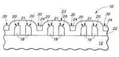
- Substrate 10is depicted as comprising material 12 which will ultimately be processed through a mask pattern formed thereover.
- Material 12may be homogenous or non-homogenous, for example comprising multiple different composition regions and/or layers.
- Spaced first features 14have been formed over substrate 12 . Any suitable material is contemplated, and whether homogenous or non-homogenous. In the context of this document, “spaced” refers to the lateral direction as opposed to vertically or otherwise. Spaced first features 14 may be patterned/formed by any existing or yet-to-be-developed manner, with photolithographic patterning using photoresist (whether positive, negative or dual-tone resist resulting from single or multi-pattern lithography) being an example. Further, spaced first features 14 may be formed by any technique described below. In one example, spaced first features 14 may be in the form of elongated lines, for example running parallel one another over at least some portion of the substrate as would be viewed in a top-down view (not shown).
- spaced first features 14may result from lateral etching/trimming of wider features.
- FIG. 2depicts substrate 10 at a processing step prior to that of FIG. 1 .
- spaced mask features 16for example comprising, consisting essentially of, or consisting of photoresist, having been fabricated over substrate 12 in a repeating pattern of a pitch “P”.
- Pitch Pmay be equal to, greater than, or less than the minimum photolithographic resolution with which substrate 10 is fabricated.
- spaced mask features 16 of FIG. 2have been laterally trimmed to reduce their respective widths to produce the example construction of FIG. 1 which comprises spaced first features 14 .
- Suchmay be conducted by an isotropic etch which removes material approximately equally from the sides and tops of spaced mask features 16 .
- chemistries and conditionsmay be used which tend to etch greater material from the lateral sides of spaced mask features 16 than from the respective tops.
- chemistries and conditionsmay be used which tend to etch greater material from the tops of spaced mask features 16 than from the lateral sides.
- the construction depicted by FIG. 1can be derived by plasma etching the substrate of FIG. 2 within an inductively coupled reactor.
- Example etching parameters which will achieve essentially isotropic etching where material of spaced mask features 16 is photoresist and/or other organic-comprising materialare pressure from about 2 mTorr to about 50 mTorr, substrate temperature from about 0° C. to about 110° C., source power from about 150 watts to about 500 watts, and bias voltage at less than or equal to about 25 volts.
- An example etching gasis a combination of Cl 2 from about 20 sccm to about 100 sccm and O 2 from about 10 sccm to about 50 sccm.
- spaced mask features 16comprises photoresist
- material of spaced mask features 16comprises photoresist
- example parameter ranges in an inductively coupled reactorinclude pressure from about 2 mTorr to about 20 mTorr, source power from about 150 watts to about 500 watts, bias voltage at less than or equal to about 25 volts, substrate temperature of from about 0° C. to about 110° C., Cl 2 and/or HBr flow from about 20 sccm to about 100 sccm, O 2 flow from about 5 sccm to about 20 sccm, and CF 4 flow from about 80 sccm to about 120 sccm.
- the stated etchingprovide greater removal from the top of the spaced mask features than from the sides, for example to either achieve equal elevation and width reduction or more elevation than width reduction.
- the example parameters for achieving greater etch rate in the vertical direction as opposed to the lateral directioninclude pressure from about 2 mTorr to about 20 mTorr, temperature from about 0° C. to about 100° C., source power from about 150 watts to about 300 watts, bias voltage at greater than or equal to about 200 volts, Cl 2 and/or HBr flow from about 20 sccm to about 100 sccm, and O 2 flow from about 10 sccm to about 20 sccm.
- FIGS. 1 and 2 embodimentsdepict the respective features as having equal shapes and widths relative one another in the depicted cross section, as well as equal spacing therebetween. Such is not, however, required in this or other embodiments.
- a material 18has been deposited as part of substrate 10 , and from which anisotropically etched spacers will be formed. Such may be etchably different from the material of spaced first features 14 , and may be conductive, semiconductive or insulative, including any combination thereof. Examples include silicon dioxide, silicon nitride, organic antireflective coatings, inorganic antireflective coatings, polysilicon, titanium or titanium nitride, including any combination thereof. Referring to FIG. 4 , material 18 has been anisotropically etched to form spacers 20 on sidewalls of spaced first features 14 .
- spaced first features 14have been removed from substrate 10 to form spaced second features which comprise spacers 20 .
- the material of spaced first features 14comprised photoresist and/or other organic material
- O 2 plasma etchingwill remove material 14 from between spacers 20 .
- the removal of material 14may or may not etch some of spacers 20 , with negligible such removal being shown in FIG. 5 to form spaced second features 20 .
- FIGS. 1 and 4depict one example embodiment wherein first features 14 are equally spaced from each adjacent of the first features ( FIG. 1 ), and second features 20 are not equally spaced from each adjacent of the second features. Alternate embodiments are contemplated.
- first features 14may be equally spaced from each adjacent of the first features and second features 20 may be equally spaced from each adjacent of the second features.
- FIG. 5depicts respective closest pairs 21 of two immediately adjacent of second features 20 having a respective space between each two of a pair 21 .
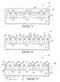
- first material 22has been deposited over spaced second features 20 , and may be of some different composition from that of spaced second features 20 .
- Material 22may or may not be homogenous.
- Example materialsinclude any of those described above for spacer-forming material 18 .
- first material 22has a non-planar outermost surface 23 , and has been deposited to completely fill space between closest pairs 21 of two immediately adjacent of second features 20 .
- a second material 24has been deposited over first material 23 , and is of some different composition from that of first material 22 and from that of spaced second features 20 .
- Second material 24has a planar outermost surface 25 .
- Suchmay, for example, result from the inherent deposition of material 24 in a liquid-fill manner, or from deposition of one or more conformal layers followed by some sort of polish-back or etch-back thereof.
- Example second materials 24include photoresist and other polymers, for example polystyrene, polymethylmethacrylate and polysiloxane. Material 24 may or may not be homogenous.
- first material 22has been removed to expose first material 22 and form regions of spaced second material 30 received over first material 22 .
- Any suitable etching technique and conditionscan be selected by the artisan. Some of material 22 may or may not be etched during the processing to produce the construction of FIG. 8 .
- first material 22has been etched from between spaced second material 30 and spaced third features 32 have been formed which comprise spaced second material 30 received over first material 22 .
- Third features 32are spaced from second features 20 .
- Any suitable substantially anisotropic etching chemistry and conditionscan be selected by the artisan for producing the FIG. 9 construction.
- FIG. 9depicts one example embodiment where a mask pattern 35 has been formed over substrate 12 and which comprises spaced second features 20 and spaced third features 32 . Such also depicts an example embodiment wherein pairs 21 of immediately adjacent spaced second features 20 alternate with individual of spaced third features 32 .
- FIGS. 1-9 embodimentsdepict mask pattern 35 ( FIG. 9 ) having been formed to have a pitch which is one-third (an integer factor of 3) that of pitch “P” of spaced mask features 16 in FIG. 2 .
- Any degree of pitch reduction (including non-integer fractional reduction) in FIGS. 1-9 , or otherwise,will of course be in large part determined on the degree of any lateral trimming that may occur of spaced features (for example in forming the substrate of FIG. 2 from that of FIG. 1 ) in combination with thickness of the deposited layers to produce the features and the spaces between features.
- FIG. 4impacts the width of spaced second features 20 .
- the deposition thickness of first material 22 in significant partdetermines spacing between second features 20 and third features 32 .
- some or all of spaced second features 20 and/or spaced third features 32may be further laterally trimmed after forming the FIG. 9 construction. Further by way of example, spaced second features 20 of FIG. 4 and/or FIG. 5 may be laterally trimmed.
- the mask pattern comprising the spaced second features and the spaced third featuresis used to process the substrate received elevationally there-below through such mask pattern.
- Such processingmay constitute any existing or yet-to-be developed technique, with etching and/or ion implanting being specific examples.
- FIG. 10depicts one example with such processing wherein mask pattern 35 has been used as an etch mask while etching into material 12 of substrate 10 .
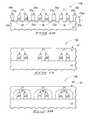
- FIG. 11depicts an alternate embodiment substrate fragment 10 a corresponding in processing sequence to that of FIG. 6 .
- Like numerals from the first described embodimentshave been utilized where appropriate, with construction differences being indicated with the suffix “a” or with different numerals. While the suffix “a” indicates different construction, example material for such constructions is the same as used in the above embodiments for the same numerals without the suffix “a”.
- first material 22 ahas been deposited much thinner than that depicted by deposition of material 22 in FIG. 6 to less than completely fill space between closest pairs 21 of two immediately adjacent of second features 20 .
- FIGS. 11 and 12depict one embodiment wherein first material 22 a has been deposited to a minimum thickness T which is less than that of second material 24 and less than maximum width of spaced second features 20 .
- first material 22 ahas been etched from between spaced second material 30 a and third spaced features 32 a have been formed which comprise spaced second material 30 a received over first material 22 a .
- Third features 32 aare spaced from second features 20 .
- FIG. 14depicts an example mask pattern 35 a having one of third features 32 a received between each of adjacent of second features 20 .
- Substrate 12may be processed through the mask pattern 35 a of FIG. 14 which comprises spaced second features 20 and spaced third features 32 a , for example by etching, ion implanting, and/or other processes as described above.
- spaced third features 32 a in mask pattern 35 aare not of the same size/shape.
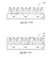
- FIG. 15depicts additional processing of substrate 10 a to produce a mask pattern 35 aa .
- Suchmay be formed by laterally trimming width of third features 32 a after the etching of first material 22 a of FIG. 14 .
- all of only some of the third featuresmay be removed to form the mask pattern prior to processing substrate material there-below.
- FIG. 15depicts lateral trimming the third features 32 a which are received between the furthest spaced of second features 20 which has also resulted in complete removal of third features 32 a which were received between closest pairs 21 of adjacent second features 20 .
- substrate 10 ahas been processed through mask pattern 35 aa .
- the example processing depicted in FIG. 16is that of ion implantation, forming implanted regions 36 .
- An embodiment of the inventionencompasses a method of fabricating a substrate which includes forming first and second spaced features over a substrate.
- features 32 a in FIG. 14may be considered as spaced first features
- features 20 in FIG. 14may be considered as spaced second features.
- the first spaced featureshave elevationally outermost regions which are different in composition from elevationally outermost regions of the second spaced features.
- the first and second spaced featuresalternate with one another.
- FIG. 14depicts such a construction where spaced features 32 a are considered as first spaced features and spaced features 20 are considered as second spaced features.
- the second featuresmay or may not be homogenous.
- the first featurescomprise a second material received over a different composition first material.
- the second featuresare of a composition which is different from that of the first and second materials.
- every other first featureis removed from the substrate and pairs of immediately adjacent second features are formed which alternate with individual of remaining of the first features.
- FIG. 15depicts such an embodiment, wherein pairs 21 of immediately adjacent second features 20 alternate with individual of remaining of features 32 a .
- the removingcomprises etching.
- the processing in producing a substratesuch as shown in FIG. 15 may occur by laterally etching the first and second materials selectively relative to second features 20 to remove every other first feature 32 a from substrate 10 a .
- Suchhas also reduced width of remaining of features 32 a , thereby forming pairs 21 of immediately adjacent second features 20 which alternate with individual of the remaining of features 32 a .
- Chemistries and conditionscan be selected by the artisan to achieve such etching, with the above-described examples in producing the substrate of FIG. 1 from that of FIG. 2 being but examples.
- the act of removingis by etching
- no etch maskis received over features 32 a during the act of etching.
- no etch maskis received anywhere over the substrate during such etching.
- the substrateis processed through a mask pattern comprising the pairs of immediately adjacent second features which alternate with individual of the remaining of the first features.
- FIG. 16depicts such example processing with respect to a mask pattern 35 aa.
- FIGS. 17-22Additional embodiments of methods of fabricating a substrate are next described with reference to FIGS. 17-22 with respect to a substrate fragment 10 b .
- Like numerals with respect to the above-described embodimentsare utilized where appropriate, with differences in construction being indicated with the suffix “b” or with different numerals. While the suffix “b” indicates different construction, example material for such constructions is the same as used in the above embodiments for the same numerals without the suffix “b”.
- FIG. 17depicts alternate processing to that of FIGS. 6 and 11 above, and wherein an alterable material 40 has been formed over spaced second features 20 . Alterable material 40 interacts selectively or uniformly with certain materials with which it forms an interface.
- Alterable material 40may be cast onto a pre-patterned surface (for example as shown) and may be conformal or non-conformal. Casting via spin-casting, dip-casting, drop-casting, or similar, are examples.
- the alterable materialwill be altered with material from the spaced second features to form altered material on sidewalls of the spaced second features.
- the altered materialmay form spontaneously upon deposition of the alterable material, or be subsequently activated, for example via thermal, photonic, electronic, ionic (including acid-based chemistry) treatments, by way of examples only. Accordingly, the altering may occur during deposition and/or after deposition. In one embodiment, no altering occurs until after completion of the deposition of the alterable material.
- alteringmay be self-limiting in the case of a limiting reagent or equilibrium conditions, or kinetically arrested if reactants are in excess.
- Alterable material 40may have a planar outermost surface or a non-planar outermost surface, with an example planar outermost surface 42 being depicted in FIG. 17 .
- Alterable material 40may or may not be homogenous.
- Material 40may be similar to a class of materials available from Clariant International, Ltd. as so-called “AZ R” materials, such as the materials designated as AZ R200TM, AZ R500TM and AZ R600TM.
- the “AZ R” materialscontain organic compositions which cross-link upon exposure to acid released from chemically-amplified resist. Accordingly for example, such materials constitute an example alterable material where material of spaced second features 20 comprises chemically-amplified resist. More specifically, an “AZ R” material may be coated across photoresist, and subsequently the resist may be baked at a temperature of from about 100° C. to about 120° C. to diffuse acid from the resist into the alterable material to form chemical cross-links within regions of the alterable material proximate the resist.
- Portions of the material adjacent the resistare thus selectively hardened relative to other portions of material that are not sufficiently proximate the resist.
- the materialmay then be exposed to conditions which selectively remove the non-hardened portions relative to the hardened portions.
- Such removalmay be accomplished utilizing, for example, 10% isopropyl alcohol in deionized water, or a solution marketed as “SOLUTION CTM” by Clariant International, Ltd.
- SOLUTION CTMClariant International, Ltd.
- Processes utilizing the “AZ R” materialsare sometimes considered examples of RELACS (Resolution Enhancement Lithography Assisted by Chemical Shrink) processes.
- alterable material 40may be similar to the “AZ R” materials in that it may comprise a similar or identical organic composition which is altered (for instance, forms cross-links) upon exposure to one or more substances (for instance, acid) released from material 20 over which material 40 lies when the substrate is baked.
- material 40may also contain one or more components disbursed in the organic composition which are provided to chemically change material 40 relative to material of features 20 (for example, photoresist in embodiments where material of features 20 may be selectively removed relative to material 40 ).
- Components which may be disbursed in an organic composition of a material 40may include one or more of titanium, carbon, fluorine, bromine, silicon and germanium. Any carbon disbursed in the organic composition may be part of a carbide compound so it is chemically different from bulk carbon of the organic composition. Any fluorine and/or bromine may be, for example, comprised of hydrofluoric acid and hydrobromic acid.
- the components disbursed in an organic composition of a material 40include one or more inorganic components, such as, for example, silicon, germanium, metals (for instance, titanium, tungsten, platinum, etc.) and/or metal-containing compounds (for instance, metal nitride, metal silicide, etc.).
- alterable material 40may be considered to have one or more inorganic components disbursed in an organic “AZ R”-type composition.
- alterable material 40may comprise other than organic and other than “AZ R”-type compositions, for example as explained below.
- alterable material 40may be similar to the “AZ R” materials in that it may comprise a similar or identical organic composition which is altered (for instance, forms cross-links) upon exposure to one or more substances (for instance, acid) released from material 20 over which material 40 lies when the substrate is baked.
- material 40may also contain one or more components dispersed in the organic composition which are provided to chemically change material 40 relative to material of features 20 (for example, photoresist in embodiments where material of features 20 may be selectively removed relative to material 40 ).
- Components which may be dispersed in an organic composition of a material 40may include one or more of titanium, carbon, fluorine, bromine, silicon and germanium. Any carbon dispersed in the organic composition may be part of a carbide compound so it is chemically different from bulk carbon of the organic composition. Any fluorine and/or bromine may be, for example, comprised of hydrofluoric acid and hydrobromic acid.
- the components dispersed in an organic composition of a material 40include one or more inorganic components, such as, for example, silicon, germanium, metals (for instance, titanium, tungsten, platinum, etc.) and/or metal-containing compounds (for instance, metal nitride, metal silicide, etc.).
- alterable material 40may be considered to have one or more inorganic components dispersed in an organic “AZ R”-type composition.
- alterable material 40may comprise other than organic and other than “AZ R”-type compositions, for example as explained below.
- substrate 10 bhas been subjected to conditions which cause inter-diffusion of materials 20 and 40 proximate spaced second features 20 .
- Some substance of material 20alters material 40 to form altered material 44 proximate spaced second features 20 .
- the alterable materialis capable of being altered with material from the spaced second features to form altered material on sidewalls of the spaced second features, for example as shown in FIG. 18 .
- the alteringalters a portion of the alterable material 40 adjacent each of spaced second features 20 to form altered material 44 while leaving portions of the alterable material distal from spaced second features unaltered.
- FIG. 18also depicts an embodiment wherein altered material 44 has been formed elevationally over spaced second features 20 . Altered material 44 may or may not be homogenous.
- material of spaced second features 20comprises chemically-amplified photoresist, and the substance from such photoresist which imparts the altering of material 40 is acid.
- the acidmay be caused to be released from photoresist by baking semiconductor substrate 10 b at a temperature of at least about 100° C.
- the acidforms cross-links with “AZ R”-type composition of material 40 .
- the amount of cross-linking, and the distance that the cross-linking spreads from spaced features 20may be adjusted by modifying one or both of bake time and bake temperature.
- an example alterable material 40is a refractory metal, such as titanium, to result in a reaction ultimately to form the altered material to comprise a metal silicide.
- a refractory metalsuch as titanium
- un-reacted distal portions of material 40(not shown) which were not altered to form material 44 have been removed, for example by etching, selectively relative to altered material 44 .
- Suitable chemistries and conditionsmay be selected by the artisan depending upon composition of materials 40 , 44 and 12 .
- such removalmay be accomplished utilizing isopropyl alcohol and/or SOLUTION CTM as discussed above.
- material 40may comprise additional components dispersed in an “AZ R”-type composition, such components may simply rinse away as the non-altered regions of material 40 are removed. Alternately, such additional components may be removed with solvents which remove the additional components.
- hydrofluoric acidmay be utilized during removal of the non-altered regions of material 40 to ensure that the silicon dioxide of the non-altered regions is removed in addition to the “AZ R”-type composition of the non-altered regions.
- second material 24 bhas been deposited over altered material 44 , with second material 24 b being of some different composition from that of altered material 44 and from that of spaced second features 20 .
- altered material 44(not shown) has been etched from between spaced second material 30 b and spaced third features 32 b have been formed which comprise spaced second material 30 b .
- Third features 32 bare spaced from second features 20 .
- FIG. 22depicts a mask pattern 35 b which is used to process substrate 12 there-through, for example by etching and/or ion implanting and/or other processing, whether existing or yet-to-be developed.
- material 40 of FIG. 18might be processed such that only a portion thereof is removed to expose altered material 44 and form spaced alterable material as opposed to deposition of material 24 b and removing a portion thereof.
- material 40 of FIG. 18could be removed to directly produce the construction of FIG. 21 wherein material 24 b is substituted by material 40 .
- altered material 44would be etched from between the spaced alterable material and third features would be formed which comprise the spaced alterable material, with the third features being spaced from the second features.
- the construction of FIG. 22could be formed wherein material 24 b is substituted by spaced alterable material 40 after material 44 of FIG. 21 has been removed.
- FIGS. 23-31Additional embodiments are next described with reference to FIGS. 23-31 with respect to a substrate fragment 10 c .
- Like numerals from the above-described embodimentshave been utilized where appropriate, with construction differences being indicated with the suffix “c” or with different numerals. While the suffix “c” indicates different construction, example material for such constructions is the same as used in the above embodiments for the same numerals without the suffix “c”.
- spaced first features 16 chave been formed over substrate 12 .
- An alterable material 40 chas been deposited over spaced first features 16 c.
- alterable material 40 chas been altered with material from spaced first features 16 c to form altered material 44 c on sidewalls of spaced first features 16 c .
- alteringmay occur during deposition of alterable material 40 c and/or after completion of deposition of alterable material 40 c .
- no alteringoccurs until after completion of deposition of alterable material 40 c , for example essentially as depicted in the processing of the substrate of FIG. 23 to that of FIG. 24 .
- altered material 44 chas been anisotropically etched to form second spaced features 20 c.
- spaced first features 16 c(not shown) have been removed from the substrate leaving at least part of second spaced features 20 c which comprise altered material 44 c.
- a first material 22 chas been deposited over spaced second features 20 c , and which is of some different composition from that of spaced second features 20 c and has a non-planar outermost surface 23 c.
- a second material 24 chas been deposited over first material 22 c , with second material 24 c being of some different composition from that of first material 22 c and from that of spaced second features 20 c.
- first material 22 chas been etched from between spaced second material 30 c , and spaced third features 32 c have been formed which comprise spaced second material 24 c .
- Third features 32 care spaced from second features 20 c .
- the FIGS. 23-31 embodimentshows a starting pitch Q in FIG. 23 and a resultant pitch in FIG. 31 of one-fourth of Q (an integer factor of 4).
- Other multiplicationincluding non-integer fractional multiplication, may also result depending on thickness of the deposited materials and any laterally trimming of the formed features.
- FIG. 31depicts an example mask pattern 35 c comprising spaced second features 20 c and spaced third features 32 c through which substrate 12 may be processed, for example as described above.
- FIG. 32depicts alternate processing with respect to a substrate fragment 10 d in the processing sequence of FIG. 28 .
- Like numerals from the above-described embodimentshave been utilized where appropriate, with construction differences being indicated with the suffix “d” or with different numerals. While the suffix “d” indicates different construction, example material for such constructions is the same as used in the above embodiments for the same numerals without the suffix “d”.
- material 40 c of FIG. 23may be considered as first alterable material which was formed over spaced first features 16 c , and which was altered with material from spaced first features 16 c to form a first altered material 44 c on sidewalls of spaced first features 16 c .
- Spaced first features 16 chave been removed from the substrate and spaced second features 20 d were formed which comprise first altered material 44 , which is designated as 44 d in FIG. 32 .
- a second alterable material 60has been formed over spaced second features 20 d .
- Composition and attributes of second alterable material 60are the same as that described above for alterable material 40 and depending at least in part on composition of spaced second features 20 d.
- second alterable material 60has been altered with first altered material 44 d from spaced second features/first altered material 20 d to form second altered material 62 on sidewalls of spaced second features 20 d .
- Composition and attributes of second altered material 62are the same as that described above for altered material 44 .
- unaltered second alterable material 60(not shown) has been removed from the substrate selectively relative to second altered material 62 .
- Third material 24 dhas been formed over second altered material 62 .
- Third material 24 dis of some different composition from that of second altered material 62 and from that of spaced second features 20 d.
- third material 24 dhas been removed to expose second altered material 62 and form spaced third material 30 d.
- FIG. 37depicts an example mask pattern 35 d comprising spaced second features 20 d and spaced third features 32 d through which substrate material 12 received elevationally inward of mask pattern 35 d can be processed, for example as described above.
- second alterable material 60 of FIG. 33might be processed such that only a portion thereof is removed to expose second altered material 62 and form spaced second alterable material as opposed to deposition of material 24 d and removing a portion thereof.
- material 60 of FIG. 33could be removed to directly produce the construction of FIG. 36 wherein material 24 d is substituted by second alterable material 60 .
- second altered material 62is etched from between the spaced second alterable material and spaced third features are formed which comprise such spaced second alterable material.
- the construction of FIG. 37may be created where second alterable material is substituted for third material 24 d.
Landscapes
- Engineering & Computer Science (AREA)
- Computer Hardware Design (AREA)
- Manufacturing & Machinery (AREA)
- Physics & Mathematics (AREA)
- Microelectronics & Electronic Packaging (AREA)
- Condensed Matter Physics & Semiconductors (AREA)
- General Physics & Mathematics (AREA)
- Power Engineering (AREA)
- Chemical & Material Sciences (AREA)
- Inorganic Chemistry (AREA)
- General Chemical & Material Sciences (AREA)
- Chemical Kinetics & Catalysis (AREA)
- Drying Of Semiconductors (AREA)
- Exposure Of Semiconductors, Excluding Electron Or Ion Beam Exposure (AREA)
- Internal Circuitry In Semiconductor Integrated Circuit Devices (AREA)
- Micromachines (AREA)
Abstract
Description
Claims (48)
Priority Applications (1)
| Application Number | Priority Date | Filing Date | Title |
|---|---|---|---|
| US13/596,430US8603884B2 (en) | 2008-12-04 | 2012-08-28 | Methods of fabricating substrates |
Applications Claiming Priority (2)
| Application Number | Priority Date | Filing Date | Title |
|---|---|---|---|
| US12/328,435US8273634B2 (en) | 2008-12-04 | 2008-12-04 | Methods of fabricating substrates |
| US13/596,430US8603884B2 (en) | 2008-12-04 | 2012-08-28 | Methods of fabricating substrates |
Related Parent Applications (1)
| Application Number | Title | Priority Date | Filing Date |
|---|---|---|---|
| US12/328,435ContinuationUS8273634B2 (en) | 2008-12-04 | 2008-12-04 | Methods of fabricating substrates |
Publications (2)
| Publication Number | Publication Date |
|---|---|
| US20120322269A1 US20120322269A1 (en) | 2012-12-20 |
| US8603884B2true US8603884B2 (en) | 2013-12-10 |
Family
ID=42231566
Family Applications (2)
| Application Number | Title | Priority Date | Filing Date |
|---|---|---|---|
| US12/328,435Active2030-07-19US8273634B2 (en) | 2008-12-04 | 2008-12-04 | Methods of fabricating substrates |
| US13/596,430ActiveUS8603884B2 (en) | 2008-12-04 | 2012-08-28 | Methods of fabricating substrates |
Family Applications Before (1)
| Application Number | Title | Priority Date | Filing Date |
|---|---|---|---|
| US12/328,435Active2030-07-19US8273634B2 (en) | 2008-12-04 | 2008-12-04 | Methods of fabricating substrates |
Country Status (8)
| Country | Link |
|---|---|
| US (2) | US8273634B2 (en) |
| EP (1) | EP2353174A4 (en) |
| JP (1) | JP5618216B2 (en) |
| KR (1) | KR101252966B1 (en) |
| CN (1) | CN102239540B (en) |
| SG (1) | SG171926A1 (en) |
| TW (1) | TWI441279B (en) |
| WO (1) | WO2010065251A2 (en) |
Cited By (4)
| Publication number | Priority date | Publication date | Assignee | Title |
|---|---|---|---|---|
| US20150093902A1 (en)* | 2013-10-01 | 2015-04-02 | Taiwan Semiconductor Manufacturing Company, Ltd. | Self-Aligned Patterning Process |
| US10062571B2 (en) | 2016-01-26 | 2018-08-28 | Samsung Electronics Co., Ltd. | Method of manufacturing semiconductor device |
| US10460938B2 (en) | 2016-04-14 | 2019-10-29 | Tokyo Electron Limited | Method for patterning a substrate using a layer with multiple materials |
| US10622256B2 (en) | 2015-04-15 | 2020-04-14 | Samsung Electronics Co., Ltd. | Method of manufacturing semiconductor device using multiple patterning techniques |
Families Citing this family (308)
| Publication number | Priority date | Publication date | Assignee | Title |
|---|---|---|---|---|
| US8852851B2 (en) | 2006-07-10 | 2014-10-07 | Micron Technology, Inc. | Pitch reduction technology using alternating spacer depositions during the formation of a semiconductor device and systems including same |
| US7989307B2 (en) | 2008-05-05 | 2011-08-02 | Micron Technology, Inc. | Methods of forming isolated active areas, trenches, and conductive lines in semiconductor structures and semiconductor structures including the same |
| US10151981B2 (en) | 2008-05-22 | 2018-12-11 | Micron Technology, Inc. | Methods of forming structures supported by semiconductor substrates |
| US8796155B2 (en)* | 2008-12-04 | 2014-08-05 | Micron Technology, Inc. | Methods of fabricating substrates |
| US8247302B2 (en) | 2008-12-04 | 2012-08-21 | Micron Technology, Inc. | Methods of fabricating substrates |
| US8273634B2 (en)* | 2008-12-04 | 2012-09-25 | Micron Technology, Inc. | Methods of fabricating substrates |
| US8268543B2 (en)* | 2009-03-23 | 2012-09-18 | Micron Technology, Inc. | Methods of forming patterns on substrates |
| US9330934B2 (en) | 2009-05-18 | 2016-05-03 | Micron Technology, Inc. | Methods of forming patterns on substrates |
| US8912097B2 (en)* | 2009-08-20 | 2014-12-16 | Varian Semiconductor Equipment Associates, Inc. | Method and system for patterning a substrate |
| US20110129991A1 (en)* | 2009-12-02 | 2011-06-02 | Kyle Armstrong | Methods Of Patterning Materials, And Methods Of Forming Memory Cells |
| US8039340B2 (en) | 2010-03-09 | 2011-10-18 | Micron Technology, Inc. | Methods of forming an array of memory cells, methods of forming a plurality of field effect transistors, methods of forming source/drain regions and isolation trenches, and methods of forming a series of spaced trenches into a substrate |
| US8518788B2 (en) | 2010-08-11 | 2013-08-27 | Micron Technology, Inc. | Methods of forming a plurality of capacitors |
| US8455341B2 (en) | 2010-09-02 | 2013-06-04 | Micron Technology, Inc. | Methods of forming features of integrated circuitry |
| US8288083B2 (en) | 2010-11-05 | 2012-10-16 | Micron Technology, Inc. | Methods of forming patterned masks |
| US8575032B2 (en) | 2011-05-05 | 2013-11-05 | Micron Technology, Inc. | Methods of forming a pattern on a substrate |
| US20130023129A1 (en) | 2011-07-20 | 2013-01-24 | Asm America, Inc. | Pressure transmitter for a semiconductor processing environment |
| US9385132B2 (en)* | 2011-08-25 | 2016-07-05 | Micron Technology, Inc. | Arrays of recessed access devices, methods of forming recessed access gate constructions, and methods of forming isolation gate constructions in the fabrication of recessed access devices |
| US9076680B2 (en) | 2011-10-18 | 2015-07-07 | Micron Technology, Inc. | Integrated circuitry, methods of forming capacitors, and methods of forming integrated circuitry comprising an array of capacitors and circuitry peripheral to the array |
| US9177794B2 (en) | 2012-01-13 | 2015-11-03 | Micron Technology, Inc. | Methods of patterning substrates |
| US8741781B2 (en)* | 2012-06-21 | 2014-06-03 | Micron Technology, Inc. | Methods of forming semiconductor constructions |
| US8629048B1 (en) | 2012-07-06 | 2014-01-14 | Micron Technology, Inc. | Methods of forming a pattern on a substrate |
| US8765612B2 (en)* | 2012-09-14 | 2014-07-01 | Nanya Technology Corporation | Double patterning process |
| US10714315B2 (en) | 2012-10-12 | 2020-07-14 | Asm Ip Holdings B.V. | Semiconductor reaction chamber showerhead |
| US9362133B2 (en)* | 2012-12-14 | 2016-06-07 | Lam Research Corporation | Method for forming a mask by etching conformal film on patterned ashable hardmask |
| US20160376700A1 (en) | 2013-02-01 | 2016-12-29 | Asm Ip Holding B.V. | System for treatment of deposition reactor |
| US9005463B2 (en) | 2013-05-29 | 2015-04-14 | Micron Technology, Inc. | Methods of forming a substrate opening |
| CN104425225A (en)* | 2013-09-04 | 2015-03-18 | 中芯国际集成电路制造(上海)有限公司 | Forming method for triple graphs |
| US9136106B2 (en) | 2013-12-19 | 2015-09-15 | Taiwan Semiconductor Manufacturing Company, Ltd. | Method for integrated circuit patterning |
| US11015245B2 (en) | 2014-03-19 | 2021-05-25 | Asm Ip Holding B.V. | Gas-phase reactor and system having exhaust plenum and components thereof |
| US9997405B2 (en) | 2014-09-30 | 2018-06-12 | Lam Research Corporation | Feature fill with nucleation inhibition |
| US10941490B2 (en) | 2014-10-07 | 2021-03-09 | Asm Ip Holding B.V. | Multiple temperature range susceptor, assembly, reactor and system including the susceptor, and methods of using the same |
| JP6502705B2 (en)* | 2015-03-03 | 2019-04-17 | キヤノン株式会社 | Method of formation |
| US10276355B2 (en) | 2015-03-12 | 2019-04-30 | Asm Ip Holding B.V. | Multi-zone reactor, system including the reactor, and method of using the same |
| US20160314964A1 (en) | 2015-04-21 | 2016-10-27 | Lam Research Corporation | Gap fill using carbon-based films |
| US10458018B2 (en) | 2015-06-26 | 2019-10-29 | Asm Ip Holding B.V. | Structures including metal carbide material, devices including the structures, and methods of forming same |
| US9911693B2 (en) | 2015-08-28 | 2018-03-06 | Micron Technology, Inc. | Semiconductor devices including conductive lines and methods of forming the semiconductor devices |
| US10211308B2 (en) | 2015-10-21 | 2019-02-19 | Asm Ip Holding B.V. | NbMC layers |
| US11139308B2 (en) | 2015-12-29 | 2021-10-05 | Asm Ip Holding B.V. | Atomic layer deposition of III-V compounds to form V-NAND devices |
| US10529554B2 (en) | 2016-02-19 | 2020-01-07 | Asm Ip Holding B.V. | Method for forming silicon nitride film selectively on sidewalls or flat surfaces of trenches |
| US10343920B2 (en) | 2016-03-18 | 2019-07-09 | Asm Ip Holding B.V. | Aligned carbon nanotubes |
| KR102328551B1 (en)* | 2016-04-29 | 2021-11-17 | 도쿄엘렉트론가부시키가이샤 | A method of patterning a substrate using a plurality of layers of material |
| US10367080B2 (en) | 2016-05-02 | 2019-07-30 | Asm Ip Holding B.V. | Method of forming a germanium oxynitride film |
| US11453943B2 (en) | 2016-05-25 | 2022-09-27 | Asm Ip Holding B.V. | Method for forming carbon-containing silicon/metal oxide or nitride film by ALD using silicon precursor and hydrocarbon precursor |
| US10612137B2 (en) | 2016-07-08 | 2020-04-07 | Asm Ip Holdings B.V. | Organic reactants for atomic layer deposition |
| US9859151B1 (en) | 2016-07-08 | 2018-01-02 | Asm Ip Holding B.V. | Selective film deposition method to form air gaps |
| US9887082B1 (en) | 2016-07-28 | 2018-02-06 | Asm Ip Holding B.V. | Method and apparatus for filling a gap |
| US9812320B1 (en) | 2016-07-28 | 2017-11-07 | Asm Ip Holding B.V. | Method and apparatus for filling a gap |
| KR102532607B1 (en) | 2016-07-28 | 2023-05-15 | 에이에스엠 아이피 홀딩 비.브이. | Substrate processing apparatus and method of operating the same |
| US11532757B2 (en) | 2016-10-27 | 2022-12-20 | Asm Ip Holding B.V. | Deposition of charge trapping layers |
| US10714350B2 (en) | 2016-11-01 | 2020-07-14 | ASM IP Holdings, B.V. | Methods for forming a transition metal niobium nitride film on a substrate by atomic layer deposition and related semiconductor device structures |
| KR102546317B1 (en) | 2016-11-15 | 2023-06-21 | 에이에스엠 아이피 홀딩 비.브이. | Gas supply unit and substrate processing apparatus including the same |
| KR102762543B1 (en) | 2016-12-14 | 2025-02-05 | 에이에스엠 아이피 홀딩 비.브이. | Substrate processing apparatus |
| US11581186B2 (en) | 2016-12-15 | 2023-02-14 | Asm Ip Holding B.V. | Sequential infiltration synthesis apparatus |
| US11447861B2 (en) | 2016-12-15 | 2022-09-20 | Asm Ip Holding B.V. | Sequential infiltration synthesis apparatus and a method of forming a patterned structure |
| KR102700194B1 (en) | 2016-12-19 | 2024-08-28 | 에이에스엠 아이피 홀딩 비.브이. | Substrate processing apparatus |
| US10269558B2 (en) | 2016-12-22 | 2019-04-23 | Asm Ip Holding B.V. | Method of forming a structure on a substrate |
| US11390950B2 (en) | 2017-01-10 | 2022-07-19 | Asm Ip Holding B.V. | Reactor system and method to reduce residue buildup during a film deposition process |
| US10468261B2 (en) | 2017-02-15 | 2019-11-05 | Asm Ip Holding B.V. | Methods for forming a metallic film on a substrate by cyclical deposition and related semiconductor device structures |
| US10529563B2 (en) | 2017-03-29 | 2020-01-07 | Asm Ip Holdings B.V. | Method for forming doped metal oxide films on a substrate by cyclical deposition and related semiconductor device structures |
| KR102457289B1 (en)* | 2017-04-25 | 2022-10-21 | 에이에스엠 아이피 홀딩 비.브이. | Method for depositing a thin film and manufacturing a semiconductor device |
| US10770286B2 (en) | 2017-05-08 | 2020-09-08 | Asm Ip Holdings B.V. | Methods for selectively forming a silicon nitride film on a substrate and related semiconductor device structures |
| US12040200B2 (en) | 2017-06-20 | 2024-07-16 | Asm Ip Holding B.V. | Semiconductor processing apparatus and methods for calibrating a semiconductor processing apparatus |
| US11306395B2 (en) | 2017-06-28 | 2022-04-19 | Asm Ip Holding B.V. | Methods for depositing a transition metal nitride film on a substrate by atomic layer deposition and related deposition apparatus |
| KR20190009245A (en) | 2017-07-18 | 2019-01-28 | 에이에스엠 아이피 홀딩 비.브이. | Methods for forming a semiconductor device structure and related semiconductor device structures |
| US11374112B2 (en) | 2017-07-19 | 2022-06-28 | Asm Ip Holding B.V. | Method for depositing a group IV semiconductor and related semiconductor device structures |
| US11018002B2 (en) | 2017-07-19 | 2021-05-25 | Asm Ip Holding B.V. | Method for selectively depositing a Group IV semiconductor and related semiconductor device structures |
| US10541333B2 (en) | 2017-07-19 | 2020-01-21 | Asm Ip Holding B.V. | Method for depositing a group IV semiconductor and related semiconductor device structures |
| US10590535B2 (en) | 2017-07-26 | 2020-03-17 | Asm Ip Holdings B.V. | Chemical treatment, deposition and/or infiltration apparatus and method for using the same |
| TWI815813B (en) | 2017-08-04 | 2023-09-21 | 荷蘭商Asm智慧財產控股公司 | Showerhead assembly for distributing a gas within a reaction chamber |
| US10692741B2 (en) | 2017-08-08 | 2020-06-23 | Asm Ip Holdings B.V. | Radiation shield |
| US10770336B2 (en) | 2017-08-08 | 2020-09-08 | Asm Ip Holding B.V. | Substrate lift mechanism and reactor including same |
| US11139191B2 (en) | 2017-08-09 | 2021-10-05 | Asm Ip Holding B.V. | Storage apparatus for storing cassettes for substrates and processing apparatus equipped therewith |
| US11769682B2 (en) | 2017-08-09 | 2023-09-26 | Asm Ip Holding B.V. | Storage apparatus for storing cassettes for substrates and processing apparatus equipped therewith |
| US11830730B2 (en) | 2017-08-29 | 2023-11-28 | Asm Ip Holding B.V. | Layer forming method and apparatus |
| US11295980B2 (en) | 2017-08-30 | 2022-04-05 | Asm Ip Holding B.V. | Methods for depositing a molybdenum metal film over a dielectric surface of a substrate by a cyclical deposition process and related semiconductor device structures |
| US11056344B2 (en) | 2017-08-30 | 2021-07-06 | Asm Ip Holding B.V. | Layer forming method |
| KR102491945B1 (en) | 2017-08-30 | 2023-01-26 | 에이에스엠 아이피 홀딩 비.브이. | Substrate processing apparatus |
| US10658205B2 (en) | 2017-09-28 | 2020-05-19 | Asm Ip Holdings B.V. | Chemical dispensing apparatus and methods for dispensing a chemical to a reaction chamber |
| US10403504B2 (en) | 2017-10-05 | 2019-09-03 | Asm Ip Holding B.V. | Method for selectively depositing a metallic film on a substrate |
| US10923344B2 (en) | 2017-10-30 | 2021-02-16 | Asm Ip Holding B.V. | Methods for forming a semiconductor structure and related semiconductor structures |
| US11022879B2 (en) | 2017-11-24 | 2021-06-01 | Asm Ip Holding B.V. | Method of forming an enhanced unexposed photoresist layer |
| CN111344522B (en) | 2017-11-27 | 2022-04-12 | 阿斯莫Ip控股公司 | Including clean mini-environment device |
| WO2019103613A1 (en) | 2017-11-27 | 2019-05-31 | Asm Ip Holding B.V. | A storage device for storing wafer cassettes for use with a batch furnace |
| US11127594B2 (en)* | 2017-12-19 | 2021-09-21 | Tokyo Electron Limited | Manufacturing methods for mandrel pull from spacers for multi-color patterning |
| JP2019121750A (en)* | 2018-01-11 | 2019-07-22 | 東京エレクトロン株式会社 | Etching method and etching apparatus |
| US10872771B2 (en) | 2018-01-16 | 2020-12-22 | Asm Ip Holding B. V. | Method for depositing a material film on a substrate within a reaction chamber by a cyclical deposition process and related device structures |
| TWI799494B (en) | 2018-01-19 | 2023-04-21 | 荷蘭商Asm 智慧財產控股公司 | Deposition method |
| KR102695659B1 (en) | 2018-01-19 | 2024-08-14 | 에이에스엠 아이피 홀딩 비.브이. | Method for depositing a gap filling layer by plasma assisted deposition |
| US11081345B2 (en) | 2018-02-06 | 2021-08-03 | Asm Ip Holding B.V. | Method of post-deposition treatment for silicon oxide film |
| US10896820B2 (en) | 2018-02-14 | 2021-01-19 | Asm Ip Holding B.V. | Method for depositing a ruthenium-containing film on a substrate by a cyclical deposition process |
| WO2019158960A1 (en) | 2018-02-14 | 2019-08-22 | Asm Ip Holding B.V. | A method for depositing a ruthenium-containing film on a substrate by a cyclical deposition process |
| US10731249B2 (en) | 2018-02-15 | 2020-08-04 | Asm Ip Holding B.V. | Method of forming a transition metal containing film on a substrate by a cyclical deposition process, a method for supplying a transition metal halide compound to a reaction chamber, and related vapor deposition apparatus |
| KR102636427B1 (en) | 2018-02-20 | 2024-02-13 | 에이에스엠 아이피 홀딩 비.브이. | Substrate processing method and apparatus |
| US10975470B2 (en) | 2018-02-23 | 2021-04-13 | Asm Ip Holding B.V. | Apparatus for detecting or monitoring for a chemical precursor in a high temperature environment |
| US11473195B2 (en) | 2018-03-01 | 2022-10-18 | Asm Ip Holding B.V. | Semiconductor processing apparatus and a method for processing a substrate |
| US11629406B2 (en) | 2018-03-09 | 2023-04-18 | Asm Ip Holding B.V. | Semiconductor processing apparatus comprising one or more pyrometers for measuring a temperature of a substrate during transfer of the substrate |
| US11114283B2 (en) | 2018-03-16 | 2021-09-07 | Asm Ip Holding B.V. | Reactor, system including the reactor, and methods of manufacturing and using same |
| KR102646467B1 (en) | 2018-03-27 | 2024-03-11 | 에이에스엠 아이피 홀딩 비.브이. | Method of forming an electrode on a substrate and a semiconductor device structure including an electrode |
| US11230766B2 (en) | 2018-03-29 | 2022-01-25 | Asm Ip Holding B.V. | Substrate processing apparatus and method |
| US11088002B2 (en) | 2018-03-29 | 2021-08-10 | Asm Ip Holding B.V. | Substrate rack and a substrate processing system and method |
| KR102600229B1 (en) | 2018-04-09 | 2023-11-10 | 에이에스엠 아이피 홀딩 비.브이. | Substrate supporting device, substrate processing apparatus including the same and substrate processing method |
| US12025484B2 (en) | 2018-05-08 | 2024-07-02 | Asm Ip Holding B.V. | Thin film forming method |
| TWI811348B (en) | 2018-05-08 | 2023-08-11 | 荷蘭商Asm 智慧財產控股公司 | Methods for depositing an oxide film on a substrate by a cyclical deposition process and related device structures |
| US12272527B2 (en) | 2018-05-09 | 2025-04-08 | Asm Ip Holding B.V. | Apparatus for use with hydrogen radicals and method of using same |
| KR102596988B1 (en) | 2018-05-28 | 2023-10-31 | 에이에스엠 아이피 홀딩 비.브이. | Method of processing a substrate and a device manufactured by the same |
| US11718913B2 (en) | 2018-06-04 | 2023-08-08 | Asm Ip Holding B.V. | Gas distribution system and reactor system including same |
| TWI840362B (en) | 2018-06-04 | 2024-05-01 | 荷蘭商Asm Ip私人控股有限公司 | Wafer handling chamber with moisture reduction |
| US11286562B2 (en) | 2018-06-08 | 2022-03-29 | Asm Ip Holding B.V. | Gas-phase chemical reactor and method of using same |
| KR102568797B1 (en) | 2018-06-21 | 2023-08-21 | 에이에스엠 아이피 홀딩 비.브이. | Substrate processing system |
| US10797133B2 (en) | 2018-06-21 | 2020-10-06 | Asm Ip Holding B.V. | Method for depositing a phosphorus doped silicon arsenide film and related semiconductor device structures |
| TWI873894B (en) | 2018-06-27 | 2025-02-21 | 荷蘭商Asm Ip私人控股有限公司 | Cyclic deposition methods for forming metal-containing material and films and structures including the metal-containing material |
| KR102854019B1 (en) | 2018-06-27 | 2025-09-02 | 에이에스엠 아이피 홀딩 비.브이. | Periodic deposition method for forming a metal-containing material and films and structures comprising the metal-containing material |
| US10612136B2 (en) | 2018-06-29 | 2020-04-07 | ASM IP Holding, B.V. | Temperature-controlled flange and reactor system including same |
| US10755922B2 (en) | 2018-07-03 | 2020-08-25 | Asm Ip Holding B.V. | Method for depositing silicon-free carbon-containing film as gap-fill layer by pulse plasma-assisted deposition |
| US10388513B1 (en) | 2018-07-03 | 2019-08-20 | Asm Ip Holding B.V. | Method for depositing silicon-free carbon-containing film as gap-fill layer by pulse plasma-assisted deposition |
| US11053591B2 (en) | 2018-08-06 | 2021-07-06 | Asm Ip Holding B.V. | Multi-port gas injection system and reactor system including same |
| US11430674B2 (en) | 2018-08-22 | 2022-08-30 | Asm Ip Holding B.V. | Sensor array, apparatus for dispensing a vapor phase reactant to a reaction chamber and related methods |
| US11024523B2 (en) | 2018-09-11 | 2021-06-01 | Asm Ip Holding B.V. | Substrate processing apparatus and method |
| KR102707956B1 (en) | 2018-09-11 | 2024-09-19 | 에이에스엠 아이피 홀딩 비.브이. | Method for deposition of a thin film |
| US11049751B2 (en) | 2018-09-14 | 2021-06-29 | Asm Ip Holding B.V. | Cassette supply system to store and handle cassettes and processing apparatus equipped therewith |
| CN110970344B (en) | 2018-10-01 | 2024-10-25 | Asmip控股有限公司 | Substrate holding apparatus, system comprising the same and method of using the same |
| US11232963B2 (en) | 2018-10-03 | 2022-01-25 | Asm Ip Holding B.V. | Substrate processing apparatus and method |
| KR102592699B1 (en) | 2018-10-08 | 2023-10-23 | 에이에스엠 아이피 홀딩 비.브이. | Substrate support unit and apparatuses for depositing thin film and processing the substrate including the same |
| KR102546322B1 (en) | 2018-10-19 | 2023-06-21 | 에이에스엠 아이피 홀딩 비.브이. | Substrate processing apparatus and substrate processing method |
| KR102605121B1 (en) | 2018-10-19 | 2023-11-23 | 에이에스엠 아이피 홀딩 비.브이. | Substrate processing apparatus and substrate processing method |
| USD948463S1 (en) | 2018-10-24 | 2022-04-12 | Asm Ip Holding B.V. | Susceptor for semiconductor substrate supporting apparatus |
| US12378665B2 (en) | 2018-10-26 | 2025-08-05 | Asm Ip Holding B.V. | High temperature coatings for a preclean and etch apparatus and related methods |
| US11087997B2 (en) | 2018-10-31 | 2021-08-10 | Asm Ip Holding B.V. | Substrate processing apparatus for processing substrates |
| KR102748291B1 (en) | 2018-11-02 | 2024-12-31 | 에이에스엠 아이피 홀딩 비.브이. | Substrate support unit and substrate processing apparatus including the same |
| US11572620B2 (en) | 2018-11-06 | 2023-02-07 | Asm Ip Holding B.V. | Methods for selectively depositing an amorphous silicon film on a substrate |
| US11031242B2 (en) | 2018-11-07 | 2021-06-08 | Asm Ip Holding B.V. | Methods for depositing a boron doped silicon germanium film |
| US10818758B2 (en) | 2018-11-16 | 2020-10-27 | Asm Ip Holding B.V. | Methods for forming a metal silicate film on a substrate in a reaction chamber and related semiconductor device structures |
| US10847366B2 (en) | 2018-11-16 | 2020-11-24 | Asm Ip Holding B.V. | Methods for depositing a transition metal chalcogenide film on a substrate by a cyclical deposition process |
| US12040199B2 (en) | 2018-11-28 | 2024-07-16 | Asm Ip Holding B.V. | Substrate processing apparatus for processing substrates |
| US11217444B2 (en) | 2018-11-30 | 2022-01-04 | Asm Ip Holding B.V. | Method for forming an ultraviolet radiation responsive metal oxide-containing film |
| KR102636428B1 (en) | 2018-12-04 | 2024-02-13 | 에이에스엠 아이피 홀딩 비.브이. | A method for cleaning a substrate processing apparatus |
| US11158513B2 (en) | 2018-12-13 | 2021-10-26 | Asm Ip Holding B.V. | Methods for forming a rhenium-containing film on a substrate by a cyclical deposition process and related semiconductor device structures |
| TWI874340B (en) | 2018-12-14 | 2025-03-01 | 荷蘭商Asm Ip私人控股有限公司 | Method of forming device structure, structure formed by the method and system for performing the method |
| CN111384172B (en)* | 2018-12-29 | 2024-01-26 | 中芯国际集成电路制造(上海)有限公司 | Semiconductor devices and methods of forming the same |
| TWI866480B (en) | 2019-01-17 | 2024-12-11 | 荷蘭商Asm Ip 私人控股有限公司 | Methods of forming a transition metal containing film on a substrate by a cyclical deposition process |
| KR102727227B1 (en) | 2019-01-22 | 2024-11-07 | 에이에스엠 아이피 홀딩 비.브이. | Semiconductor processing device |
| CN111524788B (en) | 2019-02-01 | 2023-11-24 | Asm Ip私人控股有限公司 | Method for forming topologically selective films of silicon oxide |
| TWI845607B (en) | 2019-02-20 | 2024-06-21 | 荷蘭商Asm Ip私人控股有限公司 | Cyclical deposition method and apparatus for filling a recess formed within a substrate surface |
| TWI873122B (en) | 2019-02-20 | 2025-02-21 | 荷蘭商Asm Ip私人控股有限公司 | Method of filling a recess formed within a surface of a substrate, semiconductor structure formed according to the method, and semiconductor processing apparatus |
| KR102626263B1 (en) | 2019-02-20 | 2024-01-16 | 에이에스엠 아이피 홀딩 비.브이. | Cyclical deposition method including treatment step and apparatus for same |
| TWI838458B (en) | 2019-02-20 | 2024-04-11 | 荷蘭商Asm Ip私人控股有限公司 | Apparatus and methods for plug fill deposition in 3-d nand applications |
| TWI842826B (en) | 2019-02-22 | 2024-05-21 | 荷蘭商Asm Ip私人控股有限公司 | Substrate processing apparatus and method for processing substrate |
| US11742198B2 (en) | 2019-03-08 | 2023-08-29 | Asm Ip Holding B.V. | Structure including SiOCN layer and method of forming same |
| KR102858005B1 (en) | 2019-03-08 | 2025-09-09 | 에이에스엠 아이피 홀딩 비.브이. | Method for Selective Deposition of Silicon Nitride Layer and Structure Including Selectively-Deposited Silicon Nitride Layer |
| KR102782593B1 (en) | 2019-03-08 | 2025-03-14 | 에이에스엠 아이피 홀딩 비.브이. | Structure Including SiOC Layer and Method of Forming Same |
| JP2020167398A (en) | 2019-03-28 | 2020-10-08 | エーエスエム・アイピー・ホールディング・ベー・フェー | Door openers and substrate processing equipment provided with door openers |
| KR102809999B1 (en) | 2019-04-01 | 2025-05-19 | 에이에스엠 아이피 홀딩 비.브이. | Method of manufacturing semiconductor device |
| KR20200123380A (en) | 2019-04-19 | 2020-10-29 | 에이에스엠 아이피 홀딩 비.브이. | Layer forming method and apparatus |
| KR20200125453A (en) | 2019-04-24 | 2020-11-04 | 에이에스엠 아이피 홀딩 비.브이. | Gas-phase reactor system and method of using same |
| US11289326B2 (en) | 2019-05-07 | 2022-03-29 | Asm Ip Holding B.V. | Method for reforming amorphous carbon polymer film |
| KR20200130121A (en) | 2019-05-07 | 2020-11-18 | 에이에스엠 아이피 홀딩 비.브이. | Chemical source vessel with dip tube |
| KR20200130652A (en) | 2019-05-10 | 2020-11-19 | 에이에스엠 아이피 홀딩 비.브이. | Method of depositing material onto a surface and structure formed according to the method |
| JP7612342B2 (en) | 2019-05-16 | 2025-01-14 | エーエスエム・アイピー・ホールディング・ベー・フェー | Wafer boat handling apparatus, vertical batch furnace and method |
| JP7598201B2 (en) | 2019-05-16 | 2024-12-11 | エーエスエム・アイピー・ホールディング・ベー・フェー | Wafer boat handling apparatus, vertical batch furnace and method |
| USD975665S1 (en) | 2019-05-17 | 2023-01-17 | Asm Ip Holding B.V. | Susceptor shaft |
| USD947913S1 (en) | 2019-05-17 | 2022-04-05 | Asm Ip Holding B.V. | Susceptor shaft |
| USD935572S1 (en) | 2019-05-24 | 2021-11-09 | Asm Ip Holding B.V. | Gas channel plate |
| USD922229S1 (en) | 2019-06-05 | 2021-06-15 | Asm Ip Holding B.V. | Device for controlling a temperature of a gas supply unit |
| KR20200141002A (en) | 2019-06-06 | 2020-12-17 | 에이에스엠 아이피 홀딩 비.브이. | Method of using a gas-phase reactor system including analyzing exhausted gas |
| KR20200141931A (en) | 2019-06-10 | 2020-12-21 | 에이에스엠 아이피 홀딩 비.브이. | Method for cleaning quartz epitaxial chambers |
| KR20200143254A (en) | 2019-06-11 | 2020-12-23 | 에이에스엠 아이피 홀딩 비.브이. | Method of forming an electronic structure using an reforming gas, system for performing the method, and structure formed using the method |
| USD944946S1 (en) | 2019-06-14 | 2022-03-01 | Asm Ip Holding B.V. | Shower plate |
| USD931978S1 (en) | 2019-06-27 | 2021-09-28 | Asm Ip Holding B.V. | Showerhead vacuum transport |
| KR20210005515A (en) | 2019-07-03 | 2021-01-14 | 에이에스엠 아이피 홀딩 비.브이. | Temperature control assembly for substrate processing apparatus and method of using same |
| JP7499079B2 (en) | 2019-07-09 | 2024-06-13 | エーエスエム・アイピー・ホールディング・ベー・フェー | Plasma device using coaxial waveguide and substrate processing method |
| CN112216646A (en) | 2019-07-10 | 2021-01-12 | Asm Ip私人控股有限公司 | Substrate supporting assembly and substrate processing device comprising same |
| KR20210010307A (en) | 2019-07-16 | 2021-01-27 | 에이에스엠 아이피 홀딩 비.브이. | Substrate processing apparatus |
| KR102860110B1 (en) | 2019-07-17 | 2025-09-16 | 에이에스엠 아이피 홀딩 비.브이. | Methods of forming silicon germanium structures |
| KR20210010816A (en) | 2019-07-17 | 2021-01-28 | 에이에스엠 아이피 홀딩 비.브이. | Radical assist ignition plasma system and method |
| US11643724B2 (en) | 2019-07-18 | 2023-05-09 | Asm Ip Holding B.V. | Method of forming structures using a neutral beam |
| TWI839544B (en) | 2019-07-19 | 2024-04-21 | 荷蘭商Asm Ip私人控股有限公司 | Method of forming topology-controlled amorphous carbon polymer film |
| KR20210010817A (en) | 2019-07-19 | 2021-01-28 | 에이에스엠 아이피 홀딩 비.브이. | Method of Forming Topology-Controlled Amorphous Carbon Polymer Film |
| TWI851767B (en) | 2019-07-29 | 2024-08-11 | 荷蘭商Asm Ip私人控股有限公司 | Methods for selective deposition utilizing n-type dopants and/or alternative dopants to achieve high dopant incorporation |
| CN112309899A (en) | 2019-07-30 | 2021-02-02 | Asm Ip私人控股有限公司 | Substrate processing apparatus |
| CN112309900A (en) | 2019-07-30 | 2021-02-02 | Asm Ip私人控股有限公司 | Substrate processing apparatus |
| US12169361B2 (en) | 2019-07-30 | 2024-12-17 | Asm Ip Holding B.V. | Substrate processing apparatus and method |
| US11587814B2 (en) | 2019-07-31 | 2023-02-21 | Asm Ip Holding B.V. | Vertical batch furnace assembly |
| US11227782B2 (en) | 2019-07-31 | 2022-01-18 | Asm Ip Holding B.V. | Vertical batch furnace assembly |
| US11587815B2 (en) | 2019-07-31 | 2023-02-21 | Asm Ip Holding B.V. | Vertical batch furnace assembly |
| CN112323048B (en) | 2019-08-05 | 2024-02-09 | Asm Ip私人控股有限公司 | Liquid level sensor for chemical source container |
| CN112342526A (en) | 2019-08-09 | 2021-02-09 | Asm Ip私人控股有限公司 | Heater assembly including cooling device and method of using same |
| USD965524S1 (en) | 2019-08-19 | 2022-10-04 | Asm Ip Holding B.V. | Susceptor support |
| USD965044S1 (en) | 2019-08-19 | 2022-09-27 | Asm Ip Holding B.V. | Susceptor shaft |
| JP2021031769A (en) | 2019-08-21 | 2021-03-01 | エーエスエム アイピー ホールディング ビー.ブイ. | Production apparatus of mixed gas of film deposition raw material and film deposition apparatus |
| USD930782S1 (en) | 2019-08-22 | 2021-09-14 | Asm Ip Holding B.V. | Gas distributor |
| USD949319S1 (en) | 2019-08-22 | 2022-04-19 | Asm Ip Holding B.V. | Exhaust duct |
| USD940837S1 (en) | 2019-08-22 | 2022-01-11 | Asm Ip Holding B.V. | Electrode |
| USD979506S1 (en) | 2019-08-22 | 2023-02-28 | Asm Ip Holding B.V. | Insulator |
| KR20210024423A (en) | 2019-08-22 | 2021-03-05 | 에이에스엠 아이피 홀딩 비.브이. | Method for forming a structure with a hole |
| KR20210024420A (en) | 2019-08-23 | 2021-03-05 | 에이에스엠 아이피 홀딩 비.브이. | Method for depositing silicon oxide film having improved quality by peald using bis(diethylamino)silane |
| US11286558B2 (en) | 2019-08-23 | 2022-03-29 | Asm Ip Holding B.V. | Methods for depositing a molybdenum nitride film on a surface of a substrate by a cyclical deposition process and related semiconductor device structures including a molybdenum nitride film |
| KR102806450B1 (en) | 2019-09-04 | 2025-05-12 | 에이에스엠 아이피 홀딩 비.브이. | Methods for selective deposition using a sacrificial capping layer |
| KR102733104B1 (en) | 2019-09-05 | 2024-11-22 | 에이에스엠 아이피 홀딩 비.브이. | Substrate processing apparatus |
| US11562901B2 (en) | 2019-09-25 | 2023-01-24 | Asm Ip Holding B.V. | Substrate processing method |
| CN112593212B (en) | 2019-10-02 | 2023-12-22 | Asm Ip私人控股有限公司 | Method for forming topologically selective silicon oxide film by cyclic plasma enhanced deposition process |
| TWI846953B (en) | 2019-10-08 | 2024-07-01 | 荷蘭商Asm Ip私人控股有限公司 | Substrate processing device |
| TW202128273A (en) | 2019-10-08 | 2021-08-01 | 荷蘭商Asm Ip私人控股有限公司 | Gas injection system, reactor system, and method of depositing material on surface of substratewithin reaction chamber |
| KR20210042810A (en) | 2019-10-08 | 2021-04-20 | 에이에스엠 아이피 홀딩 비.브이. | Reactor system including a gas distribution assembly for use with activated species and method of using same |
| TWI846966B (en) | 2019-10-10 | 2024-07-01 | 荷蘭商Asm Ip私人控股有限公司 | Method of forming a photoresist underlayer and structure including same |
| US12009241B2 (en) | 2019-10-14 | 2024-06-11 | Asm Ip Holding B.V. | Vertical batch furnace assembly with detector to detect cassette |
| TWI834919B (en) | 2019-10-16 | 2024-03-11 | 荷蘭商Asm Ip私人控股有限公司 | Method of topology-selective film formation of silicon oxide |
| US11637014B2 (en) | 2019-10-17 | 2023-04-25 | Asm Ip Holding B.V. | Methods for selective deposition of doped semiconductor material |
| KR102845724B1 (en) | 2019-10-21 | 2025-08-13 | 에이에스엠 아이피 홀딩 비.브이. | Apparatus and methods for selectively etching films |
| KR20210050453A (en) | 2019-10-25 | 2021-05-07 | 에이에스엠 아이피 홀딩 비.브이. | Methods for filling a gap feature on a substrate surface and related semiconductor structures |
| US11646205B2 (en) | 2019-10-29 | 2023-05-09 | Asm Ip Holding B.V. | Methods of selectively forming n-type doped material on a surface, systems for selectively forming n-type doped material, and structures formed using same |
| KR20210054983A (en) | 2019-11-05 | 2021-05-14 | 에이에스엠 아이피 홀딩 비.브이. | Structures with doped semiconductor layers and methods and systems for forming same |
| US11501968B2 (en) | 2019-11-15 | 2022-11-15 | Asm Ip Holding B.V. | Method for providing a semiconductor device with silicon filled gaps |
| KR102861314B1 (en) | 2019-11-20 | 2025-09-17 | 에이에스엠 아이피 홀딩 비.브이. | Method of depositing carbon-containing material on a surface of a substrate, structure formed using the method, and system for forming the structure |
| US11450529B2 (en) | 2019-11-26 | 2022-09-20 | Asm Ip Holding B.V. | Methods for selectively forming a target film on a substrate comprising a first dielectric surface and a second metallic surface |
| CN112951697B (en) | 2019-11-26 | 2025-07-29 | Asmip私人控股有限公司 | Substrate processing apparatus |
| CN112885692B (en) | 2019-11-29 | 2025-08-15 | Asmip私人控股有限公司 | Substrate processing apparatus |
| CN120432376A (en) | 2019-11-29 | 2025-08-05 | Asm Ip私人控股有限公司 | Substrate processing apparatus |
| JP7527928B2 (en) | 2019-12-02 | 2024-08-05 | エーエスエム・アイピー・ホールディング・ベー・フェー | Substrate processing apparatus and substrate processing method |
| KR20210070898A (en) | 2019-12-04 | 2021-06-15 | 에이에스엠 아이피 홀딩 비.브이. | Substrate processing apparatus |
| KR20210078405A (en) | 2019-12-17 | 2021-06-28 | 에이에스엠 아이피 홀딩 비.브이. | Method of forming vanadium nitride layer and structure including the vanadium nitride layer |
| KR20210080214A (en) | 2019-12-19 | 2021-06-30 | 에이에스엠 아이피 홀딩 비.브이. | Methods for filling a gap feature on a substrate and related semiconductor structures |
| JP7730637B2 (en) | 2020-01-06 | 2025-08-28 | エーエスエム・アイピー・ホールディング・ベー・フェー | Gas delivery assembly, components thereof, and reactor system including same |
| JP7636892B2 (en) | 2020-01-06 | 2025-02-27 | エーエスエム・アイピー・ホールディング・ベー・フェー | Channeled Lift Pins |
| US11993847B2 (en) | 2020-01-08 | 2024-05-28 | Asm Ip Holding B.V. | Injector |
| KR20210093163A (en) | 2020-01-16 | 2021-07-27 | 에이에스엠 아이피 홀딩 비.브이. | Method of forming high aspect ratio features |
| KR102675856B1 (en) | 2020-01-20 | 2024-06-17 | 에이에스엠 아이피 홀딩 비.브이. | Method of forming thin film and method of modifying surface of thin film |
| TWI889744B (en) | 2020-01-29 | 2025-07-11 | 荷蘭商Asm Ip私人控股有限公司 | Contaminant trap system, and baffle plate stack |
| TW202513845A (en) | 2020-02-03 | 2025-04-01 | 荷蘭商Asm Ip私人控股有限公司 | Semiconductor structures and methods for forming the same |
| KR20210100010A (en) | 2020-02-04 | 2021-08-13 | 에이에스엠 아이피 홀딩 비.브이. | Method and apparatus for transmittance measurements of large articles |
| US11776846B2 (en) | 2020-02-07 | 2023-10-03 | Asm Ip Holding B.V. | Methods for depositing gap filling fluids and related systems and devices |
| TW202146691A (en) | 2020-02-13 | 2021-12-16 | 荷蘭商Asm Ip私人控股有限公司 | Gas distribution assembly, shower plate assembly, and method of adjusting conductance of gas to reaction chamber |
| KR20210103956A (en) | 2020-02-13 | 2021-08-24 | 에이에스엠 아이피 홀딩 비.브이. | Substrate processing apparatus including light receiving device and calibration method of light receiving device |
| TWI855223B (en) | 2020-02-17 | 2024-09-11 | 荷蘭商Asm Ip私人控股有限公司 | Method for growing phosphorous-doped silicon layer |
| CN113410160A (en) | 2020-02-28 | 2021-09-17 | Asm Ip私人控股有限公司 | System specially used for cleaning parts |
| KR20210113043A (en) | 2020-03-04 | 2021-09-15 | 에이에스엠 아이피 홀딩 비.브이. | Alignment fixture for a reactor system |
| US11876356B2 (en) | 2020-03-11 | 2024-01-16 | Asm Ip Holding B.V. | Lockout tagout assembly and system and method of using same |
| KR20210116240A (en) | 2020-03-11 | 2021-09-27 | 에이에스엠 아이피 홀딩 비.브이. | Substrate handling device with adjustable joints |
| KR102775390B1 (en) | 2020-03-12 | 2025-02-28 | 에이에스엠 아이피 홀딩 비.브이. | Method for Fabricating Layer Structure Having Target Topological Profile |
| US12173404B2 (en) | 2020-03-17 | 2024-12-24 | Asm Ip Holding B.V. | Method of depositing epitaxial material, structure formed using the method, and system for performing the method |
| KR102755229B1 (en) | 2020-04-02 | 2025-01-14 | 에이에스엠 아이피 홀딩 비.브이. | Thin film forming method |
| TWI887376B (en) | 2020-04-03 | 2025-06-21 | 荷蘭商Asm Ip私人控股有限公司 | Method for manufacturing semiconductor device |
| TWI888525B (en) | 2020-04-08 | 2025-07-01 | 荷蘭商Asm Ip私人控股有限公司 | Apparatus and methods for selectively etching silcon oxide films |
| KR20210128343A (en) | 2020-04-15 | 2021-10-26 | 에이에스엠 아이피 홀딩 비.브이. | Method of forming chromium nitride layer and structure including the chromium nitride layer |
| US11821078B2 (en) | 2020-04-15 | 2023-11-21 | Asm Ip Holding B.V. | Method for forming precoat film and method for forming silicon-containing film |
| US11996289B2 (en) | 2020-04-16 | 2024-05-28 | Asm Ip Holding B.V. | Methods of forming structures including silicon germanium and silicon layers, devices formed using the methods, and systems for performing the methods |
| KR20210130646A (en) | 2020-04-21 | 2021-11-01 | 에이에스엠 아이피 홀딩 비.브이. | Method for processing a substrate |
| KR20210132600A (en) | 2020-04-24 | 2021-11-04 | 에이에스엠 아이피 홀딩 비.브이. | Methods and systems for depositing a layer comprising vanadium, nitrogen, and a further element |
| KR20210132612A (en) | 2020-04-24 | 2021-11-04 | 에이에스엠 아이피 홀딩 비.브이. | Methods and apparatus for stabilizing vanadium compounds |
| CN113555279A (en) | 2020-04-24 | 2021-10-26 | Asm Ip私人控股有限公司 | Methods of forming vanadium nitride-containing layers and structures comprising the same |
| KR102866804B1 (en) | 2020-04-24 | 2025-09-30 | 에이에스엠 아이피 홀딩 비.브이. | Vertical batch furnace assembly comprising a cooling gas supply |
| TW202208671A (en) | 2020-04-24 | 2022-03-01 | 荷蘭商Asm Ip私人控股有限公司 | Methods of forming structures including vanadium boride and vanadium phosphide layers |
| KR102783898B1 (en) | 2020-04-29 | 2025-03-18 | 에이에스엠 아이피 홀딩 비.브이. | Solid source precursor vessel |
| KR20210134869A (en) | 2020-05-01 | 2021-11-11 | 에이에스엠 아이피 홀딩 비.브이. | Fast FOUP swapping with a FOUP handler |
| JP7726664B2 (en) | 2020-05-04 | 2025-08-20 | エーエスエム・アイピー・ホールディング・ベー・フェー | Substrate processing system for processing a substrate |
| KR102788543B1 (en) | 2020-05-13 | 2025-03-27 | 에이에스엠 아이피 홀딩 비.브이. | Laser alignment fixture for a reactor system |
| TW202146699A (en) | 2020-05-15 | 2021-12-16 | 荷蘭商Asm Ip私人控股有限公司 | Method of forming a silicon germanium layer, semiconductor structure, semiconductor device, method of forming a deposition layer, and deposition system |
| KR20210143653A (en) | 2020-05-19 | 2021-11-29 | 에이에스엠 아이피 홀딩 비.브이. | Substrate processing apparatus |
| KR20210145079A (en) | 2020-05-21 | 2021-12-01 | 에이에스엠 아이피 홀딩 비.브이. | Flange and apparatus for processing substrates |
| KR102795476B1 (en) | 2020-05-21 | 2025-04-11 | 에이에스엠 아이피 홀딩 비.브이. | Structures including multiple carbon layers and methods of forming and using same |
| US11776812B2 (en)* | 2020-05-22 | 2023-10-03 | Tokyo Electron Limited | Method for pattern reduction using a staircase spacer |
| TWI873343B (en) | 2020-05-22 | 2025-02-21 | 荷蘭商Asm Ip私人控股有限公司 | Reaction system for forming thin film on substrate |
| KR20210146802A (en) | 2020-05-26 | 2021-12-06 | 에이에스엠 아이피 홀딩 비.브이. | Method for depositing boron and gallium containing silicon germanium layers |
| TWI876048B (en) | 2020-05-29 | 2025-03-11 | 荷蘭商Asm Ip私人控股有限公司 | Substrate processing device |
| TW202212620A (en) | 2020-06-02 | 2022-04-01 | 荷蘭商Asm Ip私人控股有限公司 | Apparatus for processing substrate, method of forming film, and method of controlling apparatus for processing substrate |
| TW202208659A (en) | 2020-06-16 | 2022-03-01 | 荷蘭商Asm Ip私人控股有限公司 | Method for depositing boron containing silicon germanium layers |
| TW202218133A (en) | 2020-06-24 | 2022-05-01 | 荷蘭商Asm Ip私人控股有限公司 | Method for forming a layer provided with silicon |
| TWI873359B (en) | 2020-06-30 | 2025-02-21 | 荷蘭商Asm Ip私人控股有限公司 | Substrate processing method |
| US12431354B2 (en) | 2020-07-01 | 2025-09-30 | Asm Ip Holding B.V. | Silicon nitride and silicon oxide deposition methods using fluorine inhibitor |
| TW202202649A (en) | 2020-07-08 | 2022-01-16 | 荷蘭商Asm Ip私人控股有限公司 | Substrate processing method |
| KR20220010438A (en) | 2020-07-17 | 2022-01-25 | 에이에스엠 아이피 홀딩 비.브이. | Structures and methods for use in photolithography |
| KR20220011092A (en) | 2020-07-20 | 2022-01-27 | 에이에스엠 아이피 홀딩 비.브이. | Method and system for forming structures including transition metal layers |
| TWI878570B (en) | 2020-07-20 | 2025-04-01 | 荷蘭商Asm Ip私人控股有限公司 | Method and system for depositing molybdenum layers |
| US12322591B2 (en) | 2020-07-27 | 2025-06-03 | Asm Ip Holding B.V. | Thin film deposition process |
| KR20220021863A (en) | 2020-08-14 | 2022-02-22 | 에이에스엠 아이피 홀딩 비.브이. | Method for processing a substrate |
| US12040177B2 (en) | 2020-08-18 | 2024-07-16 | Asm Ip Holding B.V. | Methods for forming a laminate film by cyclical plasma-enhanced deposition processes |
| TW202228863A (en) | 2020-08-25 | 2022-08-01 | 荷蘭商Asm Ip私人控股有限公司 | Method for cleaning a substrate, method for selectively depositing, and reaction system |
| US11725280B2 (en) | 2020-08-26 | 2023-08-15 | Asm Ip Holding B.V. | Method for forming metal silicon oxide and metal silicon oxynitride layers |
| TW202229601A (en) | 2020-08-27 | 2022-08-01 | 荷蘭商Asm Ip私人控股有限公司 | Method of forming patterned structures, method of manipulating mechanical property, device structure, and substrate processing system |
| TW202217045A (en) | 2020-09-10 | 2022-05-01 | 荷蘭商Asm Ip私人控股有限公司 | Methods for depositing gap filing fluids and related systems and devices |
| USD990534S1 (en) | 2020-09-11 | 2023-06-27 | Asm Ip Holding B.V. | Weighted lift pin |
| KR20220036866A (en) | 2020-09-16 | 2022-03-23 | 에이에스엠 아이피 홀딩 비.브이. | Silicon oxide deposition method |
| USD1012873S1 (en) | 2020-09-24 | 2024-01-30 | Asm Ip Holding B.V. | Electrode for semiconductor processing apparatus |
| TWI889903B (en) | 2020-09-25 | 2025-07-11 | 荷蘭商Asm Ip私人控股有限公司 | Semiconductor processing method |
| US12009224B2 (en) | 2020-09-29 | 2024-06-11 | Asm Ip Holding B.V. | Apparatus and method for etching metal nitrides |
| KR20220045900A (en) | 2020-10-06 | 2022-04-13 | 에이에스엠 아이피 홀딩 비.브이. | Deposition method and an apparatus for depositing a silicon-containing material |
| CN114293174A (en) | 2020-10-07 | 2022-04-08 | Asm Ip私人控股有限公司 | Gas supply unit and substrate processing apparatus including the same |
| TW202229613A (en) | 2020-10-14 | 2022-08-01 | 荷蘭商Asm Ip私人控股有限公司 | Method of depositing material on stepped structure |
| TW202232565A (en) | 2020-10-15 | 2022-08-16 | 荷蘭商Asm Ip私人控股有限公司 | Method of manufacturing semiconductor device, and substrate treatment apparatus using ether-cat |
| KR20220049742A (en)* | 2020-10-15 | 2022-04-22 | 삼성전기주식회사 | Printed circuit board |
| TW202217037A (en) | 2020-10-22 | 2022-05-01 | 荷蘭商Asm Ip私人控股有限公司 | Method of depositing vanadium metal, structure, device and a deposition assembly |
| TW202223136A (en) | 2020-10-28 | 2022-06-16 | 荷蘭商Asm Ip私人控股有限公司 | Method for forming layer on substrate, and semiconductor processing system |
| TW202229620A (en) | 2020-11-12 | 2022-08-01 | 特文特大學 | Deposition system, method for controlling reaction condition, method for depositing |
| TW202229795A (en) | 2020-11-23 | 2022-08-01 | 荷蘭商Asm Ip私人控股有限公司 | A substrate processing apparatus with an injector |
| TW202235649A (en) | 2020-11-24 | 2022-09-16 | 荷蘭商Asm Ip私人控股有限公司 | Methods for filling a gap and related systems and devices |
| TW202235675A (en) | 2020-11-30 | 2022-09-16 | 荷蘭商Asm Ip私人控股有限公司 | Injector, and substrate processing apparatus |
| US12255053B2 (en) | 2020-12-10 | 2025-03-18 | Asm Ip Holding B.V. | Methods and systems for depositing a layer |
| TW202233884A (en) | 2020-12-14 | 2022-09-01 | 荷蘭商Asm Ip私人控股有限公司 | Method of forming structures for threshold voltage control |
| US11946137B2 (en) | 2020-12-16 | 2024-04-02 | Asm Ip Holding B.V. | Runout and wobble measurement fixtures |
| TW202232639A (en) | 2020-12-18 | 2022-08-16 | 荷蘭商Asm Ip私人控股有限公司 | Wafer processing apparatus with a rotatable table |
| TW202231903A (en) | 2020-12-22 | 2022-08-16 | 荷蘭商Asm Ip私人控股有限公司 | Transition metal deposition method, transition metal layer, and deposition assembly for depositing transition metal on substrate |
| TW202242184A (en) | 2020-12-22 | 2022-11-01 | 荷蘭商Asm Ip私人控股有限公司 | Precursor capsule, precursor vessel, vapor deposition assembly, and method of loading solid precursor into precursor vessel |
| TW202226899A (en) | 2020-12-22 | 2022-07-01 | 荷蘭商Asm Ip私人控股有限公司 | Plasma treatment device having matching box |
| USD1023959S1 (en) | 2021-05-11 | 2024-04-23 | Asm Ip Holding B.V. | Electrode for substrate processing apparatus |
| USD980813S1 (en) | 2021-05-11 | 2023-03-14 | Asm Ip Holding B.V. | Gas flow control plate for substrate processing apparatus |
| USD981973S1 (en) | 2021-05-11 | 2023-03-28 | Asm Ip Holding B.V. | Reactor wall for substrate processing apparatus |
| USD980814S1 (en) | 2021-05-11 | 2023-03-14 | Asm Ip Holding B.V. | Gas distributor for substrate processing apparatus |
| USD990441S1 (en) | 2021-09-07 | 2023-06-27 | Asm Ip Holding B.V. | Gas flow control plate |
| USD1060598S1 (en) | 2021-12-03 | 2025-02-04 | Asm Ip Holding B.V. | Split showerhead cover |
Citations (213)
| Publication number | Priority date | Publication date | Assignee | Title |
|---|---|---|---|---|
| EP0171111A3 (en) | 1984-07-13 | 1987-07-22 | BELL TELEPHONE MANUFACTURING COMPANY Naamloze Vennootschap | Process to superpose two positive photoresist layers |
| US4910168A (en) | 1988-05-06 | 1990-03-20 | Mos Electronics Corporation | Method to reduce silicon area for via formation |
| US5008207A (en) | 1989-09-11 | 1991-04-16 | International Business Machines Corporation | Method of fabricating a narrow base transistor |
| US5013680A (en) | 1990-07-18 | 1991-05-07 | Micron Technology, Inc. | Process for fabricating a DRAM array having feature widths that transcend the resolution limit of available photolithography |
| US5047117A (en) | 1990-09-26 | 1991-09-10 | Micron Technology, Inc. | Method of forming a narrow self-aligned, annular opening in a masking layer |
| US5254218A (en) | 1992-04-22 | 1993-10-19 | Micron Technology, Inc. | Masking layer having narrow isolated spacings and the method for forming said masking layer and the method for forming narrow isolated trenches defined by said masking layer |
| US5328810A (en) | 1990-05-07 | 1994-07-12 | Micron Technology, Inc. | Method for reducing, by a factor or 2-N, the minimum masking pitch of a photolithographic process |
| US5372916A (en) | 1991-09-12 | 1994-12-13 | Hitachi, Ltd. | X-ray exposure method with an X-ray mask comprising phase shifter sidewalls |
| US5382315A (en)* | 1991-02-11 | 1995-01-17 | Microelectronics And Computer Technology Corporation | Method of forming etch mask using particle beam deposition |
| US5420067A (en)* | 1990-09-28 | 1995-05-30 | The United States Of America As Represented By The Secretary Of The Navy | Method of fabricatring sub-half-micron trenches and holes |
| US5429988A (en)* | 1994-06-13 | 1995-07-04 | United Microelectronics Corporation | Process for producing high density conductive lines |
| US5573837A (en) | 1992-04-22 | 1996-11-12 | Micron Technology, Inc. | Masking layer having narrow isolated spacings and the method for forming said masking layer and the method for forming narrow isolated trenches defined by said masking layer |
| US5593813A (en) | 1994-07-14 | 1997-01-14 | Hyundai Electronics Industries Co. Ltd. | Method for forming submicroscopic patterns |
| US5616510A (en) | 1992-11-02 | 1997-04-01 | Wong; Chun C. D. | Method for making multimedia storage system with highly compact memory cells |
| US5905279A (en) | 1996-04-09 | 1999-05-18 | Kabushiki Kaisha Toshiba | Low resistant trench fill for a semiconductor device |
| US5916821A (en) | 1995-07-17 | 1999-06-29 | Siemens Aktiengesellschaft | Method for producing sublithographic etching masks |
| US6063688A (en) | 1997-09-29 | 2000-05-16 | Intel Corporation | Fabrication of deep submicron structures and quantum wire transistors using hard-mask transistor width definition |
| US6087263A (en) | 1998-01-29 | 2000-07-11 | Micron Technology, Inc. | Methods of forming integrated circuitry and integrated circuitry structures |
| US6140217A (en) | 1998-07-16 | 2000-10-31 | International Business Machines Corporation | Technique for extending the limits of photolithography |
| US6207490B1 (en) | 1997-12-11 | 2001-03-27 | Samsung Electronics Co., Ltd. | Semiconductor device and method for fabricating the same |
| US6235574B1 (en) | 1999-03-22 | 2001-05-22 | Infineon North America Corp. | High performance DRAM and method of manufacture |
| US6249335B1 (en) | 1992-01-17 | 2001-06-19 | Nikon Corporation | Photo-mask and method of exposing and projection-exposing apparatus |
| US6303272B1 (en) | 1998-11-13 | 2001-10-16 | International Business Machines Corporation | Process for self-alignment of sub-critical contacts to wiring |
| US20020037617A1 (en) | 2000-06-29 | 2002-03-28 | Kim Jun Dong | Method for forming gate electrodes in a semicoductor device using formed fine patterns |
| JP3270227B2 (en) | 1993-05-26 | 2002-04-02 | 富士写真フイルム株式会社 | Electric hoist |
| US6383952B1 (en) | 2001-02-28 | 2002-05-07 | Advanced Micro Devices, Inc. | RELACS process to double the frequency or pitch of small feature formation |
| US20020094688A1 (en) | 2001-01-16 | 2002-07-18 | Semiconductor Leading Edge Technologies, Inc. | Method of forming fine patterns |
| US6429123B1 (en) | 2000-10-04 | 2002-08-06 | Vanguard International Semiconductor Corporation | Method of manufacturing buried metal lines having ultra fine features |
| US6483136B1 (en) | 1997-06-20 | 2002-11-19 | Hitachi, Ltd. | Semiconductor integrated circuit and method of fabricating the same |
| EP1273974A2 (en) | 2001-07-05 | 2003-01-08 | Tokyo Ohka Kogyo Co., Ltd. | Method for reducing a pattern dimension in a photoresist layer |
| US20030006410A1 (en) | 2000-03-01 | 2003-01-09 | Brian Doyle | Quantum wire gate device and method of making same |
| US6545904B2 (en) | 2001-03-16 | 2003-04-08 | Micron Technology, Inc. | 6f2 dram array, a dram array formed on a semiconductive substrate, a method of forming memory cells in a 6f2 dram array and a method of isolating a single row of memory cells in a 6f2 dram array |
| US6548385B1 (en) | 2002-06-12 | 2003-04-15 | Jiun-Ren Lai | Method for reducing pitch between conductive features, and structure formed using the method |
| US6548401B1 (en) | 2002-01-23 | 2003-04-15 | Micron Technology, Inc. | Semiconductor processing methods, and semiconductor constructions |
| US20030091936A1 (en) | 2001-08-31 | 2003-05-15 | Jorg Rottstegge | Process for sidewall amplification of resist structures and for the production of structures having reduced structure size |
| US6566280B1 (en) | 2002-08-26 | 2003-05-20 | Intel Corporation | Forming polymer features on a substrate |
| US6580136B2 (en) | 2001-01-30 | 2003-06-17 | International Business Machines Corporation | Method for delineation of eDRAM support device notched gate |
| KR20030049198A (en) | 2001-12-14 | 2003-06-25 | 주식회사 하이닉스반도체 | Forming method of photoresist pattern improving etching resistance by relacs material |
| KR20030056601A (en) | 2001-12-28 | 2003-07-04 | 주식회사 하이닉스반도체 | Method of forming a source line in flash memory device |
| US6599844B2 (en) | 2000-06-22 | 2003-07-29 | Hyundai Electronics Industries, Co., Ltd. | Method and forming fine patterns of semiconductor devices using passivation layers |
| US6605541B1 (en) | 1998-05-07 | 2003-08-12 | Advanced Micro Devices, Inc. | Pitch reduction using a set of offset masks |
| JP2003234279A (en) | 2002-02-08 | 2003-08-22 | Sony Corp | Forming method of resist pattern, manufacturing method of semiconductor device and forming device for resist pattern |
| US6627524B2 (en) | 2001-06-06 | 2003-09-30 | Micron Technology, Inc. | Methods of forming transistor gates; and methods of forming programmable read-only memory constructions |
| US6630379B2 (en) | 2000-06-23 | 2003-10-07 | International Business Machines Corporation | Method of manufacturing 6F2 trench capacitor DRAM cell having vertical MOSFET and 3F bitline pitch |
| US6638441B2 (en) | 2002-01-07 | 2003-10-28 | Macronix International Co., Ltd. | Method for pitch reduction |
| KR20030089063A (en) | 2002-05-16 | 2003-11-21 | 주식회사 하이닉스반도체 | Forming method of photoresist pattern |
| US6667502B1 (en) | 1999-08-31 | 2003-12-23 | Micron Technology, Inc. | Structurally-stabilized capacitors and method of making of same |
| US6703323B2 (en) | 2001-12-14 | 2004-03-09 | Hynix Semiconductor Inc | Method of inhibiting pattern collapse using a relacs material |
| US6710390B2 (en) | 1997-07-03 | 2004-03-23 | Micron Technology, Inc. | Capacitors and DRAM arrays |
| JP2004134574A (en) | 2002-10-10 | 2004-04-30 | Renesas Technology Corp | Manufacturing method of semiconductor device |
| US6734107B2 (en) | 2002-06-12 | 2004-05-11 | Macronix International Co., Ltd. | Pitch reduction in semiconductor fabrication |
| US6735132B2 (en) | 2001-07-23 | 2004-05-11 | Micron Technology, Inc. | 6F2 DRAM array with apparatus for stress testing an isolation gate and method |
| US6753220B2 (en) | 1996-11-01 | 2004-06-22 | Micron Technology, Inc. | Semiconductor processing methods of forming devices on a substrate, forming device arrays on a substrate, forming conductive lines on a substrate, and forming capacitor arrays on a substrate, and integrated circuitry |
| US6756619B2 (en) | 2002-08-26 | 2004-06-29 | Micron Technology, Inc. | Semiconductor constructions |
| KR20040057582A (en) | 2002-12-26 | 2004-07-02 | 주식회사 하이닉스반도체 | Method of forming a micro pattern having a dual damascene |
| US6774051B2 (en) | 2002-06-12 | 2004-08-10 | Macronix International Co., Ltd. | Method for reducing pitch |
| JP2004247399A (en) | 2003-02-12 | 2004-09-02 | Renesas Technology Corp | Method for manufacturing semiconductor device |
| US20040198065A1 (en) | 2003-04-04 | 2004-10-07 | Sung-Kwon Lee | Method for fabricating semiconductor device with fine patterns |
| US6826069B2 (en) | 2001-03-14 | 2004-11-30 | Atmos Corporation | Interleaved wordline architecture |
| US20040253535A1 (en) | 2002-11-20 | 2004-12-16 | Shipley Company, L.L.C. | Multilayer photoresist systems |
| US6864184B1 (en) | 2004-02-05 | 2005-03-08 | Advanced Micro Devices, Inc. | Method for reducing critical dimension attainable via the use of an organic conforming layer |
| US6872512B2 (en) | 2002-03-27 | 2005-03-29 | Nec Lcd Technologies, Ltd. | Method of forming resist pattern |
| US6905975B2 (en) | 2003-07-03 | 2005-06-14 | Micron Technology, Inc. | Methods of forming patterned compositions |
| US20050130068A1 (en) | 2003-11-21 | 2005-06-16 | Takehiro Kondoh | Pattern forming method and method for manufacturing a semiconductor device |
| US20050142497A1 (en) | 2003-12-26 | 2005-06-30 | Samsung Electronics Co., Ltd. | Method of forming a pattern in a semiconductor device and method of forming a gate using the same |
| US6916594B2 (en) | 2002-12-30 | 2005-07-12 | Hynix Semiconductor Inc. | Overcoating composition for photoresist and method for forming photoresist pattern using the same |
| US20050164478A1 (en) | 2004-01-26 | 2005-07-28 | Taiwan Semiconductor Manufacturing Co. | Novel method of trimming technology |
| US20050173740A1 (en) | 2004-02-07 | 2005-08-11 | You-Seung Jin | Multi-gate transistor formed with active patterns of uniform critical dimension |
| US20050214683A1 (en) | 2004-02-24 | 2005-09-29 | Tokyo Electron Limited | Method and apparatus for reforming film and controlling slimming amount thereof |
| US6951822B2 (en) | 2001-09-28 | 2005-10-04 | Infineon Technologies North America Corp. | Method for forming inside nitride spacer for deep trench device DRAM cell |
| US20050255696A1 (en) | 2003-05-09 | 2005-11-17 | Fujitsu Limited | Method of processing resist, semiconductor device, and method of producing the same |
| US20050272220A1 (en) | 2004-06-07 | 2005-12-08 | Carlo Waldfried | Ultraviolet curing process for spin-on dielectric materials used in pre-metal and/or shallow trench isolation applications |
| US20060011947A1 (en) | 2004-05-26 | 2006-01-19 | Werner Juengling | Semiconductor structures and memory device constructions |
| US20060024621A1 (en) | 2004-07-17 | 2006-02-02 | Infineon Technologies Ag | Method of producing a structure on the surface of a substrate |
| US20060046200A1 (en) | 2004-09-01 | 2006-03-02 | Abatchev Mirzafer K | Mask material conversion |
| US20060046484A1 (en) | 2004-09-02 | 2006-03-02 | Abatchev Mirzafer K | Method for integrated circuit fabrication using pitch multiplication |
| US20060046422A1 (en) | 2004-08-31 | 2006-03-02 | Micron Technology, Inc. | Methods for increasing photo alignment margins |
| US20060063384A1 (en) | 2004-09-23 | 2006-03-23 | Jung-Hwan Hah | Mask patterns for semiconductor device fabrication and related methods and structures |
| US7023069B2 (en) | 2003-12-19 | 2006-04-04 | Third Dimension (3D) Semiconductor, Inc. | Method for forming thick dielectric regions using etched trenches |
| CN1761063A (en) | 2004-10-14 | 2006-04-19 | 茂德科技股份有限公司 | Structure of Dynamic Random Access Memory |
| US20060088788A1 (en) | 2004-10-26 | 2006-04-27 | Takanori Kudo | Composition for coating over a photoresist pattern |
| US7037840B2 (en) | 2004-01-26 | 2006-05-02 | Micron Technology, Inc. | Methods of forming planarized surfaces over semiconductor substrates |
| US7049652B2 (en) | 2003-12-10 | 2006-05-23 | Sandisk Corporation | Pillar cell flash memory technology |
| US20060115978A1 (en) | 2004-11-30 | 2006-06-01 | Michael Specht | Charge-trapping memory cell and method for production |
| US20060118785A1 (en) | 2003-09-12 | 2006-06-08 | International Business Machines Corporation | Techniques for patterning features in semiconductor devices |
| US7064376B2 (en) | 1996-05-24 | 2006-06-20 | Jeng-Jye Shau | High performance embedded semiconductor memory devices with multiple dimension first-level bit-lines |
| US7067385B2 (en) | 2003-09-04 | 2006-06-27 | Micron Technology, Inc. | Support for vertically oriented capacitors during the formation of a semiconductor device |
| US20060154182A1 (en) | 2005-01-12 | 2006-07-13 | International Business Machines Corporation | Method for post lithographic critical dimension shrinking using post overcoat planarization |
| US7125781B2 (en) | 2003-09-04 | 2006-10-24 | Micron Technology, Inc. | Methods of forming capacitor devices |
| US20060240361A1 (en) | 2005-04-21 | 2006-10-26 | Ji-Young Lee | Method of forming small pitch pattern using double spacers |
| US20060263699A1 (en) | 2005-05-23 | 2006-11-23 | Mirzafer Abatchev | Methods for forming arrays of a small, closely spaced features |
| US20060273456A1 (en) | 2005-06-02 | 2006-12-07 | Micron Technology, Inc., A Corporation | Multiple spacer steps for pitch multiplication |
| US20060278911A1 (en) | 2005-06-14 | 2006-12-14 | Eppich Anton P | Relaxed-pitch method of aligning active area to digit line |
| US20060286795A1 (en) | 2005-06-21 | 2006-12-21 | Kabushiki Kaisha Toshiba | Method of manufacturing semiconductor device |
| US20070003878A1 (en) | 2005-03-23 | 2007-01-04 | Asml Netherlands B.V. | Reduced pitch multiple exposure process |
| US20070010058A1 (en) | 2005-07-08 | 2007-01-11 | Micron Technology, Inc. | Method and apparatus for a self-aligned recessed access device (RAD) transistor gate |
| US7166533B2 (en) | 2005-04-08 | 2007-01-23 | Infineon Technologies, Ag | Phase change memory cell defined by a pattern shrink material process |
| JP2007017993A (en) | 2006-08-22 | 2007-01-25 | Fujitsu Ltd | Resist pattern and method for manufacturing the same, and semiconductor device and method for manufacturing the same |
| US20070020565A1 (en) | 2005-07-25 | 2007-01-25 | Samsung Electronics Co., Ltd. | Methods of fabricating a semiconductor device |
| US20070026684A1 (en) | 2005-08-01 | 2007-02-01 | Stefano Parascandola | Method of producing pitch fractionizations in semiconductor technology |
| US20070023805A1 (en) | 2005-07-26 | 2007-02-01 | Wells David H | Reverse construction memory cell |
| US20070037066A1 (en) | 2005-08-09 | 2007-02-15 | Li-Tung Hsiao | Method for correcting and configuring optical mask pattern |
| US20070049011A1 (en) | 2005-09-01 | 2007-03-01 | Micron Technology, Inc., A Corporation | Method of forming isolated features using pitch multiplication |
| US20070045712A1 (en) | 2005-09-01 | 2007-03-01 | Haller Gordon A | Memory cell layout and process flow |
| US20070049035A1 (en) | 2005-08-31 | 2007-03-01 | Tran Luan C | Method of forming pitch multipled contacts |
| US20070048674A1 (en) | 2005-09-01 | 2007-03-01 | Wells David H | Methods for forming arrays of small, closely spaced features |
| US20070049030A1 (en) | 2005-09-01 | 2007-03-01 | Sandhu Gurtej S | Pitch multiplication spacers and methods of forming the same |
| US20070048930A1 (en) | 2005-09-01 | 2007-03-01 | Figura Thomas A | Peripheral gate stacks and recessed array gates |
| US20070049003A1 (en) | 2005-09-01 | 2007-03-01 | John Smythe | Semiconductor constructions and methods of forming layers |
| US20070049040A1 (en) | 2005-03-15 | 2007-03-01 | Micron Technology, Inc., A Corporation | Multiple deposition for integration of spacers in pitch multiplication process |
| US7199005B2 (en) | 2005-08-02 | 2007-04-03 | Micron Technology, Inc. | Methods of forming pluralities of capacitors |
| US20070077524A1 (en) | 2005-09-30 | 2007-04-05 | Samsung Electronics Co., Ltd. | Method for forming patterns of semiconductor device |
| US20070077743A1 (en) | 2005-09-30 | 2007-04-05 | Rao Rajesh A | Multiple fin formation |
| US7202127B2 (en) | 2004-08-27 | 2007-04-10 | Micron Technology, Inc. | Methods of forming a plurality of capacitors |
| US7202174B1 (en) | 2006-02-02 | 2007-04-10 | Hynix Semiconductor Inc. | Method of forming micro pattern in semiconductor device |
| US20070085152A1 (en) | 2005-10-14 | 2007-04-19 | Promos Technologies Pte.Ltd. Singapore | Reduced area dynamic random access memory (DRAM) cell and method for fabricating the same |
| US20070096182A1 (en) | 2004-09-10 | 2007-05-03 | Infineon Technologies Ag | Transistor, meomory cell array and method of manufacturing a transistor |
| US20070099431A1 (en) | 2005-11-01 | 2007-05-03 | Micron Technology, Inc. | Process for increasing feature density during the manufacture of a semiconductor device |
| US20070105357A1 (en) | 2005-09-01 | 2007-05-10 | Micron Technology, Inc. | Silicided recessed silicon |
| US20070123015A1 (en) | 2005-11-30 | 2007-05-31 | International Business Machines Corporation | Passive components in the back end of integrated circuits |
| US7230292B2 (en) | 2003-08-05 | 2007-06-12 | Micron Technology, Inc. | Stud electrode and process for making same |
| US20070145464A1 (en) | 2002-08-29 | 2007-06-28 | Voshell Thomas W | Random access memory device utilizing a vertically oriented select transistor |
| US20070161251A1 (en) | 2005-03-15 | 2007-07-12 | Micron Technology, Inc. | Pitch reduced patterns relative to photolithography features |
| US20070181929A1 (en) | 2005-06-27 | 2007-08-09 | Micron Technology, Inc. | Semiconductor Constructions, Memory Cells, DRAM Arrays, Electronic Systems; Methods of Forming Semiconductor Constructions; and Methods of Forming DRAM Arrays |
| US20070190463A1 (en) | 2004-09-02 | 2007-08-16 | Micron Technology, Inc. | Method to align mask patterns |
| US20070197014A1 (en) | 2006-02-17 | 2007-08-23 | Samsung Electronics Co., Ltd. | Method of fabricating semiconductor device |
| CN101026087A (en) | 2006-02-24 | 2007-08-29 | 海力士半导体有限公司 | Method for forming fine pattern of semiconductor device |
| US20070202697A1 (en) | 2006-02-24 | 2007-08-30 | Hynix Semiconductor Inc. | Method for forming fine pattern of semiconductor device |
| US20070205438A1 (en) | 2006-03-02 | 2007-09-06 | Werner Juengling | Masking process for simultaneously patterning separate regions |
| US20070205443A1 (en) | 2006-03-02 | 2007-09-06 | Werner Juengling | Vertical gated access transistor |
| US20070224537A1 (en) | 2006-03-24 | 2007-09-27 | Fujitsu Limited | Resist composition, method for forming resist pattern, and semiconductor device and method for manufacturing the same |
| US20070238053A1 (en) | 2006-04-11 | 2007-10-11 | Koji Hashimoto | Manufacturing method of semiconductor device |
| US20070238299A1 (en) | 2006-04-07 | 2007-10-11 | Micron Technology, Inc. | Simplified pitch doubling process flow |
| US20070248916A1 (en) | 2006-04-21 | 2007-10-25 | Tdk Corporation | Resist pattern forming method, thin-film pattern forming method, and microdevice manufacturing method |
| US20070261016A1 (en) | 2006-04-24 | 2007-11-08 | Sandhu Gurtej S | Masking techniques and templates for dense semiconductor fabrication |
| US20070264828A1 (en) | 2006-05-09 | 2007-11-15 | Hynix Semiconductor Inc. | Method for forming fine pattern of semiconductor device |
| US20070264830A1 (en) | 2006-05-10 | 2007-11-15 | Lam Research Corporation | Pitch reduction |
| US20070281219A1 (en) | 2006-06-01 | 2007-12-06 | Sandhu Gurtej S | Masking techniques and contact imprint reticles for dense semiconductor fabrication |
| US20070278183A1 (en) | 2006-06-02 | 2007-12-06 | Whonchee Lee | Wet etch suitable for creating square cuts in si and resulting structures |
| US20080008969A1 (en) | 2006-07-10 | 2008-01-10 | Micron Technology, Inc. | Pitch reduction technology using alternating spacer depositions during the formation of a semiconductor device and systems including same |
| US7320911B2 (en) | 2004-12-06 | 2008-01-22 | Micron Technology, Inc. | Methods of forming pluralities of capacitors |
| US20080026327A1 (en) | 2006-07-14 | 2008-01-31 | Hynix Semiconductor Inc. | Method for forming fine pattern with a double exposure technology |
| US20080032243A1 (en) | 2005-05-30 | 2008-02-07 | Hynix Semiconductor Inc. | Photoresist Coating Composition and Method for Forming Fine Contact of Semiconductor Device |
| US20080032508A1 (en) | 2006-08-07 | 2008-02-07 | Taiwan Semiconductor Manufacturing Company, Ltd. | Method and Material For Forming A Double Exposure Lithography Pattern |
| US20080044770A1 (en) | 2006-08-17 | 2008-02-21 | Fujitsu Limited | Process for forming resist pattern, semiconductor device and manufacturing method for the same |
| US20080057692A1 (en) | 2006-08-30 | 2008-03-06 | Wells David H | Single spacer process for multiplying pitch by a factor greater than two and related intermediate IC structures |
| US20080064213A1 (en) | 2006-09-12 | 2008-03-13 | Hynix Semiconductor Inc. | Method for forming a fine pattern of a semiconductor device |
| US20080063986A1 (en) | 2006-09-12 | 2008-03-13 | Hynix Semiconductor Inc. | Method of forming fine pattern of semiconductor device |
| US20080070165A1 (en) | 2006-09-14 | 2008-03-20 | Mark Fischer | Efficient pitch multiplication process |
| US20080076070A1 (en) | 2006-09-08 | 2008-03-27 | Samsung Electronics Co., Ltd. | Methods of Forming Fine Patterns In Integrated Circuits Using Atomic Layer Deposition |
| US20080085612A1 (en) | 2006-10-05 | 2008-04-10 | Micron Technology, Inc. | Method to deposit conformal low temperature SiO2 |
| US20080090416A1 (en) | 2006-10-11 | 2008-04-17 | Micro Technology, Inc. | Methods of etching polysilicon and methods of forming pluralities of capacitors |
| KR20080038963A (en) | 2006-10-31 | 2008-05-07 | 주식회사 하이닉스반도체 | Method for manufacturing a semiconductor device having a contact |
| US20080113511A1 (en) | 2006-11-10 | 2008-05-15 | Sang-Joon Park | Method of forming fine patterns using double patterning process |
| US20080113483A1 (en) | 2006-11-15 | 2008-05-15 | Micron Technology, Inc. | Methods of etching a pattern layer to form staggered heights therein and intermediate semiconductor device structures |
| US20080122125A1 (en) | 2006-11-29 | 2008-05-29 | Micron Technology, Inc. | Methods to reduce the critical dimension of semiconductor devices and partially fabricated semiconductor devices having reduced critical dimensions |
| US20080120900A1 (en) | 2006-11-29 | 2008-05-29 | Femo Operations, Lp | Systems and Methods for Repelling and/or Killing Pests Using Mulch |
| US7387939B2 (en) | 2004-07-19 | 2008-06-17 | Micron Technology, Inc. | Methods of forming semiconductor structures and capacitor devices |
| US7390750B1 (en) | 2004-03-23 | 2008-06-24 | Cypress Semiconductor Corp. | Method of patterning elements within a semiconductor topography |
| US7390749B2 (en) | 2005-11-30 | 2008-06-24 | Lam Research Corporation | Self-aligned pitch reduction |
| US7396781B2 (en) | 2005-06-09 | 2008-07-08 | Micron Technology, Inc. | Method and apparatus for adjusting feature size and position |
| US20080171446A1 (en) | 2007-01-12 | 2008-07-17 | Advanced Micro Devices, Inc. | Method of forming semiconductor device |
| US20080171438A1 (en) | 2007-01-11 | 2008-07-17 | Micron Technology, Inc. | Methods of uniformly removing silicon oxide, a method of removing a sacrifical oxide, and an intermediate semiconductor device structure |
| US20080176406A1 (en) | 2007-01-22 | 2008-07-24 | Shuji Ikeda | Methods for Fabricating Semiconductor Structures |
| US20080199806A1 (en) | 2007-02-16 | 2008-08-21 | Shin-Etsu Chemical Co., Ltd. | Patterning process and resist composition |
| US20080199814A1 (en) | 2006-12-06 | 2008-08-21 | Fujifilm Electronic Materials, U.S.A., Inc. | Device manufacturing process utilizing a double patterning process |
| US20080206950A1 (en) | 2007-02-26 | 2008-08-28 | Micron Technology, Inc. | Methods of forming a plurality of capacitors |
| US20080220600A1 (en) | 2007-03-05 | 2008-09-11 | Micron Technology, Inc. | Semiconductor constructions, methods of forming multiple lines, and methods of forming high density structures and low density structures with a single photomask |
| US7439152B2 (en) | 2004-08-27 | 2008-10-21 | Micron Technology, Inc. | Methods of forming a plurality of capacitors |
| US20080261349A1 (en) | 2005-09-01 | 2008-10-23 | Micron Technology, Inc. | Protective coating for planarization |
| US7442976B2 (en) | 2004-09-01 | 2008-10-28 | Micron Technology, Inc. | DRAM cells with vertical transistors |
| US20080292991A1 (en) | 2007-05-24 | 2008-11-27 | Advanced Micro Devices, Inc. | High fidelity multiple resist patterning |
| US20080296732A1 (en) | 2007-05-31 | 2008-12-04 | Micron Technology, Inc. | Methods of isolating array features during pitch doubling processes and semiconductor device structures having isolated array features |
| US20080305636A1 (en) | 2007-06-07 | 2008-12-11 | Samsung Electronics Co., Ltd. | Method of forming fine pattern employing self-aligned double patterning |
| US20090074958A1 (en) | 2007-09-13 | 2009-03-19 | Dequan Xiao | Polymeric nanocompositions comprising self-assembled organic quantum dots |
| US7517753B2 (en) | 2005-05-18 | 2009-04-14 | Micron Technology, Inc. | Methods of forming pluralities of capacitors |
| US7521378B2 (en) | 2004-07-01 | 2009-04-21 | Micron Technology, Inc. | Low temperature process for polysilazane oxidation/densification |
| US7521371B2 (en) | 2006-08-21 | 2009-04-21 | Micron Technology, Inc. | Methods of forming semiconductor constructions having lines |
| US7524607B2 (en) | 2003-11-17 | 2009-04-28 | Taiwan Semiconductor Manufacturing Co., Ltd. | Water soluble negative tone photoresist |
| US20090108415A1 (en) | 2007-10-31 | 2009-04-30 | Markus Lenski | Increasing etch selectivity during the patterning of a contact structure of a semiconductor device |
| US20090117739A1 (en) | 2007-11-02 | 2009-05-07 | Hynix Semiconductor Inc. | Method for forming pattern in semiconductor device |
| US20090130852A1 (en) | 2006-04-25 | 2009-05-21 | Micron Technology, Inc. | Process for improving critical dimension uniformity of integrated circuit arrays |
| US20090130612A1 (en) | 2007-11-21 | 2009-05-21 | Macronix International Co., Ltd. | Patterning process |
| US20090130601A1 (en) | 2007-11-16 | 2009-05-21 | Young-Doo Jeon | Method for fabricating semiconductor device |
| US7537866B2 (en) | 2006-05-24 | 2009-05-26 | Synopsys, Inc. | Patterning a single integrated circuit layer using multiple masks and multiple masking layers |
| US7544563B2 (en) | 2005-05-18 | 2009-06-09 | Micron Technology, Inc. | Methods of forming a plurality of capacitors |
| US7553760B2 (en) | 2006-10-19 | 2009-06-30 | International Business Machines Corporation | Sub-lithographic nano interconnect structures, and method for forming same |
| US7557015B2 (en) | 2005-03-18 | 2009-07-07 | Micron Technology, Inc. | Methods of forming pluralities of capacitors |
| US7557013B2 (en) | 2006-04-10 | 2009-07-07 | Micron Technology, Inc. | Methods of forming a plurality of capacitors |
| US20090212016A1 (en) | 2008-02-22 | 2009-08-27 | International Business Machines Corporation | Aligning polymer films |
| US20090291397A1 (en) | 2008-05-22 | 2009-11-26 | Devilliers Anton | Methods Of Forming Structures Supported By Semiconductor Substrates |
| US20090298274A1 (en) | 2008-05-29 | 2009-12-03 | Seiji Kajiwara | Method of fabricating semiconductor device |
| US20100009512A1 (en) | 2008-07-09 | 2010-01-14 | Fred Fishburn | Methods of forming a plurality of capacitors |
| US20100021573A1 (en) | 2008-07-22 | 2010-01-28 | Michael J Gonzalez | Compositions and methods for the prevention of cardiovascular disease |
| US20100028809A1 (en) | 2006-11-14 | 2010-02-04 | Nxp, B.V. | Double patterning for lithography to increase feature spatial density |
| US20100068656A1 (en) | 2008-09-15 | 2010-03-18 | Taiwan Semiconductor Manufacturing Co., Ltd. | High etch resistant material for double patterning |
| US7682924B2 (en) | 2007-08-13 | 2010-03-23 | Micron Technology, Inc. | Methods of forming a plurality of capacitors |
| US7687387B2 (en) | 2007-08-23 | 2010-03-30 | Kabushiki Kaisha Toshiba | Semiconductor device and method of manufacturing the same |
| US20100081265A1 (en) | 2008-09-30 | 2010-04-01 | Hiromitsu Mashita | Method for manufacturing semiconductor device |
| US7696076B2 (en) | 2007-05-11 | 2010-04-13 | Hynix Semiconductor Inc. | Method of fabricating flash memory device |
| US7713818B2 (en) | 2008-04-11 | 2010-05-11 | Sandisk 3D, Llc | Double patterning method |
| US20100130016A1 (en) | 2008-11-24 | 2010-05-27 | Micron Technology, Inc. | Methods of forming a masking pattern for integrated circuits |
| US20100130015A1 (en) | 2007-06-08 | 2010-05-27 | Tokyo Electron Limited | Patterning method |
| US20100144151A1 (en) | 2008-12-04 | 2010-06-10 | Scott Sills | Methods of Fabricating Substrates |
| US20100144150A1 (en) | 2008-12-04 | 2010-06-10 | Micron Technology, Inc. | Methods of Fabricating Substrates |
| US20100144153A1 (en) | 2008-12-04 | 2010-06-10 | Scott Sills | Methods of Fabricating Substrates |
| US7851135B2 (en) | 2007-11-30 | 2010-12-14 | Hynix Semiconductor Inc. | Method of forming an etching mask pattern from developed negative and positive photoresist layers |
| US20110018055A1 (en) | 2009-07-21 | 2011-01-27 | Kabushiki Kaisha Toshiba | Power semiconductor device and method for manufacturing same |
| US20110127677A1 (en) | 2008-02-15 | 2011-06-02 | Renesas Electronics Corporation | Method of manufacturing semiconductor device, and semiconductor device |
| CN101145515B (en) | 2006-09-12 | 2011-06-29 | 海力士半导体有限公司 | Method for forming a fine pattern of a semiconductor device |
| US8083958B2 (en) | 2007-12-05 | 2011-12-27 | International Business Machines Corporation | Patterning method using a combination of photolithography and copolymer self-assemblying lithography techniques |
| US8083953B2 (en) | 2007-03-06 | 2011-12-27 | Micron Technology, Inc. | Registered structure formation via the application of directed thermal energy to diblock copolymer films |
| US8440576B2 (en) | 2008-04-25 | 2013-05-14 | Macronix International Co., Ltd. | Method for pitch reduction in integrated circuit fabrication |
Family Cites Families (10)
| Publication number | Priority date | Publication date | Assignee | Title |
|---|---|---|---|---|
| JPS6435916A (en)* | 1987-07-31 | 1989-02-07 | Hitachi Ltd | Formation of fine pattern |
| JP2006245625A (en) | 1997-06-20 | 2006-09-14 | Hitachi Ltd | Semiconductor integrated circuit device and manufacturing method thereof |
| EP1048220B1 (en)* | 1999-04-26 | 2012-10-17 | Societe Des Produits Nestle S.A. | A whitened coffee concentrate |
| US7887387B2 (en)* | 2005-03-14 | 2011-02-15 | Originates, Inc. | Stuffed toy with removable and replaceable stuffing, and method for use thereof |
| EP1880410A2 (en) | 2005-05-13 | 2008-01-23 | Sachem, Inc. | Selective wet etching of oxides |
| KR100784062B1 (en) | 2006-01-20 | 2007-12-10 | 주식회사 하이닉스반도체 | Method of forming fine pattern of semiconductor device |
| US7709341B2 (en) | 2006-06-02 | 2010-05-04 | Micron Technology, Inc. | Methods of shaping vertical single crystal silicon walls and resulting structures |
| US7625776B2 (en) | 2006-06-02 | 2009-12-01 | Micron Technology, Inc. | Methods of fabricating intermediate semiconductor structures by selectively etching pockets of implanted silicon |
| KR100801078B1 (en) | 2006-06-29 | 2008-02-11 | 삼성전자주식회사 | Non-volatile memory integrated circuit device having a vertical channel and its manufacturing method |
| JP4352068B2 (en)* | 2006-09-08 | 2009-10-28 | 株式会社東芝 | Exposure method and semiconductor device manufacturing method |
- 2008
- 2008-12-04USUS12/328,435patent/US8273634B2/enactiveActive
- 2009
- 2009-11-11SGSG2011040326Apatent/SG171926A1/enunknown
- 2009-11-11WOPCT/US2009/063999patent/WO2010065251A2/enactiveApplication Filing
- 2009-11-11JPJP2011539551Apatent/JP5618216B2/enactiveActive
- 2009-11-11KRKR1020117014921Apatent/KR101252966B1/enactiveActive
- 2009-11-11CNCN200980148548.8Apatent/CN102239540B/enactiveActive
- 2009-11-11EPEP09830819.0Apatent/EP2353174A4/ennot_activeCeased
- 2009-11-24TWTW098139942Apatent/TWI441279B/enactive
- 2012
- 2012-08-28USUS13/596,430patent/US8603884B2/enactiveActive
Patent Citations (256)
| Publication number | Priority date | Publication date | Assignee | Title |
|---|---|---|---|---|
| EP0171111A3 (en) | 1984-07-13 | 1987-07-22 | BELL TELEPHONE MANUFACTURING COMPANY Naamloze Vennootschap | Process to superpose two positive photoresist layers |
| US4910168A (en) | 1988-05-06 | 1990-03-20 | Mos Electronics Corporation | Method to reduce silicon area for via formation |
| US5008207A (en) | 1989-09-11 | 1991-04-16 | International Business Machines Corporation | Method of fabricating a narrow base transistor |
| US5328810A (en) | 1990-05-07 | 1994-07-12 | Micron Technology, Inc. | Method for reducing, by a factor or 2-N, the minimum masking pitch of a photolithographic process |
| US5013680A (en) | 1990-07-18 | 1991-05-07 | Micron Technology, Inc. | Process for fabricating a DRAM array having feature widths that transcend the resolution limit of available photolithography |
| US5047117A (en) | 1990-09-26 | 1991-09-10 | Micron Technology, Inc. | Method of forming a narrow self-aligned, annular opening in a masking layer |
| US5420067A (en)* | 1990-09-28 | 1995-05-30 | The United States Of America As Represented By The Secretary Of The Navy | Method of fabricatring sub-half-micron trenches and holes |
| US5382315A (en)* | 1991-02-11 | 1995-01-17 | Microelectronics And Computer Technology Corporation | Method of forming etch mask using particle beam deposition |
| US5372916A (en) | 1991-09-12 | 1994-12-13 | Hitachi, Ltd. | X-ray exposure method with an X-ray mask comprising phase shifter sidewalls |
| US6249335B1 (en) | 1992-01-17 | 2001-06-19 | Nikon Corporation | Photo-mask and method of exposing and projection-exposing apparatus |
| US5254218A (en) | 1992-04-22 | 1993-10-19 | Micron Technology, Inc. | Masking layer having narrow isolated spacings and the method for forming said masking layer and the method for forming narrow isolated trenches defined by said masking layer |
| US5573837A (en) | 1992-04-22 | 1996-11-12 | Micron Technology, Inc. | Masking layer having narrow isolated spacings and the method for forming said masking layer and the method for forming narrow isolated trenches defined by said masking layer |
| US5616510A (en) | 1992-11-02 | 1997-04-01 | Wong; Chun C. D. | Method for making multimedia storage system with highly compact memory cells |
| JP3270227B2 (en) | 1993-05-26 | 2002-04-02 | 富士写真フイルム株式会社 | Electric hoist |
| US5429988A (en)* | 1994-06-13 | 1995-07-04 | United Microelectronics Corporation | Process for producing high density conductive lines |
| US5593813A (en) | 1994-07-14 | 1997-01-14 | Hyundai Electronics Industries Co. Ltd. | Method for forming submicroscopic patterns |
| US5916821A (en) | 1995-07-17 | 1999-06-29 | Siemens Aktiengesellschaft | Method for producing sublithographic etching masks |
| US5905279A (en) | 1996-04-09 | 1999-05-18 | Kabushiki Kaisha Toshiba | Low resistant trench fill for a semiconductor device |
| US7064376B2 (en) | 1996-05-24 | 2006-06-20 | Jeng-Jye Shau | High performance embedded semiconductor memory devices with multiple dimension first-level bit-lines |
| US6753220B2 (en) | 1996-11-01 | 2004-06-22 | Micron Technology, Inc. | Semiconductor processing methods of forming devices on a substrate, forming device arrays on a substrate, forming conductive lines on a substrate, and forming capacitor arrays on a substrate, and integrated circuitry |
| US6483136B1 (en) | 1997-06-20 | 2002-11-19 | Hitachi, Ltd. | Semiconductor integrated circuit and method of fabricating the same |
| US6649956B2 (en) | 1997-06-20 | 2003-11-18 | Hitachi, Ltd. | Semiconductor integrated circuit device and manufacturing method thereof |
| US20040043546A1 (en) | 1997-06-20 | 2004-03-04 | Makoto Yoshida | Semiconductor integrated circuit device and manufacturing method thereof |
| US7042038B2 (en) | 1997-06-20 | 2006-05-09 | Hitachi, Ltd. | Semiconductor integrated circuit device and manufacturing method thereof |
| US20030001214A1 (en) | 1997-06-20 | 2003-01-02 | Makoto Yoshida | Semiconductor integrated circuit device and manufacturing method thereof |
| US6710390B2 (en) | 1997-07-03 | 2004-03-23 | Micron Technology, Inc. | Capacitors and DRAM arrays |
| US6063688A (en) | 1997-09-29 | 2000-05-16 | Intel Corporation | Fabrication of deep submicron structures and quantum wire transistors using hard-mask transistor width definition |
| US20020043690A1 (en) | 1997-09-29 | 2002-04-18 | Doyle Brian S. | Fabrication of deep submicron structures and quantum wire transistors using hard-mask transistor width definition |
| US6207490B1 (en) | 1997-12-11 | 2001-03-27 | Samsung Electronics Co., Ltd. | Semiconductor device and method for fabricating the same |
| US6087263A (en) | 1998-01-29 | 2000-07-11 | Micron Technology, Inc. | Methods of forming integrated circuitry and integrated circuitry structures |
| US6352932B1 (en) | 1998-01-29 | 2002-03-05 | Micron Technology, Inc. | Methods of forming integrated circuitry and integrated circuitry structures |
| US6605541B1 (en) | 1998-05-07 | 2003-08-12 | Advanced Micro Devices, Inc. | Pitch reduction using a set of offset masks |
| US6140217A (en) | 1998-07-16 | 2000-10-31 | International Business Machines Corporation | Technique for extending the limits of photolithography |
| US6303272B1 (en) | 1998-11-13 | 2001-10-16 | International Business Machines Corporation | Process for self-alignment of sub-critical contacts to wiring |
| US6235574B1 (en) | 1999-03-22 | 2001-05-22 | Infineon North America Corp. | High performance DRAM and method of manufacture |
| US6667502B1 (en) | 1999-08-31 | 2003-12-23 | Micron Technology, Inc. | Structurally-stabilized capacitors and method of making of same |
| US20030006410A1 (en) | 2000-03-01 | 2003-01-09 | Brian Doyle | Quantum wire gate device and method of making same |
| US6599844B2 (en) | 2000-06-22 | 2003-07-29 | Hyundai Electronics Industries, Co., Ltd. | Method and forming fine patterns of semiconductor devices using passivation layers |
| US6630379B2 (en) | 2000-06-23 | 2003-10-07 | International Business Machines Corporation | Method of manufacturing 6F2 trench capacitor DRAM cell having vertical MOSFET and 3F bitline pitch |
| US20020037617A1 (en) | 2000-06-29 | 2002-03-28 | Kim Jun Dong | Method for forming gate electrodes in a semicoductor device using formed fine patterns |
| US6429123B1 (en) | 2000-10-04 | 2002-08-06 | Vanguard International Semiconductor Corporation | Method of manufacturing buried metal lines having ultra fine features |
| JP2002217170A (en) | 2001-01-16 | 2002-08-02 | Semiconductor Leading Edge Technologies Inc | Method of forming fine pattern, method of fabricating semiconductor device and semiconductor device |
| US20020094688A1 (en) | 2001-01-16 | 2002-07-18 | Semiconductor Leading Edge Technologies, Inc. | Method of forming fine patterns |
| US6580136B2 (en) | 2001-01-30 | 2003-06-17 | International Business Machines Corporation | Method for delineation of eDRAM support device notched gate |
| US6383952B1 (en) | 2001-02-28 | 2002-05-07 | Advanced Micro Devices, Inc. | RELACS process to double the frequency or pitch of small feature formation |
| US6826069B2 (en) | 2001-03-14 | 2004-11-30 | Atmos Corporation | Interleaved wordline architecture |
| US6545904B2 (en) | 2001-03-16 | 2003-04-08 | Micron Technology, Inc. | 6f2 dram array, a dram array formed on a semiconductive substrate, a method of forming memory cells in a 6f2 dram array and a method of isolating a single row of memory cells in a 6f2 dram array |
| US6627524B2 (en) | 2001-06-06 | 2003-09-30 | Micron Technology, Inc. | Methods of forming transistor gates; and methods of forming programmable read-only memory constructions |
| US20030008968A1 (en) | 2001-07-05 | 2003-01-09 | Yoshiki Sugeta | Method for reducing pattern dimension in photoresist layer |
| US6811817B2 (en) | 2001-07-05 | 2004-11-02 | Tokyo Ohka Kogyo Co., Ltd. | Method for reducing pattern dimension in photoresist layer |
| US20050058950A1 (en) | 2001-07-05 | 2005-03-17 | Yoshiki Sugeta | Method for reducing pattern dimension in photoresist layer |
| US20030096903A1 (en) | 2001-07-05 | 2003-05-22 | Yoshiki Sugeta | Method for reducing pattern dimension in photoresist layer |
| US20060099347A1 (en) | 2001-07-05 | 2006-05-11 | Yoshiki Sugeta | Method for reducing pattern dimension in photoresist layer |
| EP1273974A2 (en) | 2001-07-05 | 2003-01-08 | Tokyo Ohka Kogyo Co., Ltd. | Method for reducing a pattern dimension in a photoresist layer |
| US6735132B2 (en) | 2001-07-23 | 2004-05-11 | Micron Technology, Inc. | 6F2 DRAM array with apparatus for stress testing an isolation gate and method |
| US6893972B2 (en) | 2001-08-31 | 2005-05-17 | Infineon Technologies Ag | Process for sidewall amplification of resist structures and for the production of structures having reduced structure size |
| US20030091936A1 (en) | 2001-08-31 | 2003-05-15 | Jorg Rottstegge | Process for sidewall amplification of resist structures and for the production of structures having reduced structure size |
| US6951822B2 (en) | 2001-09-28 | 2005-10-04 | Infineon Technologies North America Corp. | Method for forming inside nitride spacer for deep trench device DRAM cell |
| US6703323B2 (en) | 2001-12-14 | 2004-03-09 | Hynix Semiconductor Inc | Method of inhibiting pattern collapse using a relacs material |
| KR20030049198A (en) | 2001-12-14 | 2003-06-25 | 주식회사 하이닉스반도체 | Forming method of photoresist pattern improving etching resistance by relacs material |
| KR20030056601A (en) | 2001-12-28 | 2003-07-04 | 주식회사 하이닉스반도체 | Method of forming a source line in flash memory device |
| US6638441B2 (en) | 2002-01-07 | 2003-10-28 | Macronix International Co., Ltd. | Method for pitch reduction |
| US6548401B1 (en) | 2002-01-23 | 2003-04-15 | Micron Technology, Inc. | Semiconductor processing methods, and semiconductor constructions |
| JP2003234279A (en) | 2002-02-08 | 2003-08-22 | Sony Corp | Forming method of resist pattern, manufacturing method of semiconductor device and forming device for resist pattern |
| US6872512B2 (en) | 2002-03-27 | 2005-03-29 | Nec Lcd Technologies, Ltd. | Method of forming resist pattern |
| KR20030089063A (en) | 2002-05-16 | 2003-11-21 | 주식회사 하이닉스반도체 | Forming method of photoresist pattern |
| US6734107B2 (en) | 2002-06-12 | 2004-05-11 | Macronix International Co., Ltd. | Pitch reduction in semiconductor fabrication |
| US6774051B2 (en) | 2002-06-12 | 2004-08-10 | Macronix International Co., Ltd. | Method for reducing pitch |
| US6548385B1 (en) | 2002-06-12 | 2003-04-15 | Jiun-Ren Lai | Method for reducing pitch between conductive features, and structure formed using the method |
| US6756619B2 (en) | 2002-08-26 | 2004-06-29 | Micron Technology, Inc. | Semiconductor constructions |
| US6566280B1 (en) | 2002-08-26 | 2003-05-20 | Intel Corporation | Forming polymer features on a substrate |
| US20070145464A1 (en) | 2002-08-29 | 2007-06-28 | Voshell Thomas W | Random access memory device utilizing a vertically oriented select transistor |
| JP2004134574A (en) | 2002-10-10 | 2004-04-30 | Renesas Technology Corp | Manufacturing method of semiconductor device |
| US20040253535A1 (en) | 2002-11-20 | 2004-12-16 | Shipley Company, L.L.C. | Multilayer photoresist systems |
| US7582412B2 (en) | 2002-11-20 | 2009-09-01 | Rohm And Haas Electronic Materials Llc | Multilayer photoresist systems |
| CN1550889B (en) | 2002-11-20 | 2011-08-03 | 希普雷公司 | Multilayer Photoresist System |
| KR20040057582A (en) | 2002-12-26 | 2004-07-02 | 주식회사 하이닉스반도체 | Method of forming a micro pattern having a dual damascene |
| US6916594B2 (en) | 2002-12-30 | 2005-07-12 | Hynix Semiconductor Inc. | Overcoating composition for photoresist and method for forming photoresist pattern using the same |
| JP2004247399A (en) | 2003-02-12 | 2004-09-02 | Renesas Technology Corp | Method for manufacturing semiconductor device |
| US20040198065A1 (en) | 2003-04-04 | 2004-10-07 | Sung-Kwon Lee | Method for fabricating semiconductor device with fine patterns |
| US20050255696A1 (en) | 2003-05-09 | 2005-11-17 | Fujitsu Limited | Method of processing resist, semiconductor device, and method of producing the same |
| US6905975B2 (en) | 2003-07-03 | 2005-06-14 | Micron Technology, Inc. | Methods of forming patterned compositions |
| US7230292B2 (en) | 2003-08-05 | 2007-06-12 | Micron Technology, Inc. | Stud electrode and process for making same |
| US7125781B2 (en) | 2003-09-04 | 2006-10-24 | Micron Technology, Inc. | Methods of forming capacitor devices |
| US7067385B2 (en) | 2003-09-04 | 2006-06-27 | Micron Technology, Inc. | Support for vertically oriented capacitors during the formation of a semiconductor device |
| US20060118785A1 (en) | 2003-09-12 | 2006-06-08 | International Business Machines Corporation | Techniques for patterning features in semiconductor devices |
| US7524607B2 (en) | 2003-11-17 | 2009-04-28 | Taiwan Semiconductor Manufacturing Co., Ltd. | Water soluble negative tone photoresist |
| US20050130068A1 (en) | 2003-11-21 | 2005-06-16 | Takehiro Kondoh | Pattern forming method and method for manufacturing a semiconductor device |
| US7049652B2 (en) | 2003-12-10 | 2006-05-23 | Sandisk Corporation | Pillar cell flash memory technology |
| US7023069B2 (en) | 2003-12-19 | 2006-04-04 | Third Dimension (3D) Semiconductor, Inc. | Method for forming thick dielectric regions using etched trenches |
| US7339252B2 (en) | 2003-12-19 | 2008-03-04 | Third Dimension (3D) Semiconductor, Inc. | Semiconductor having thick dielectric regions |
| US20050142497A1 (en) | 2003-12-26 | 2005-06-30 | Samsung Electronics Co., Ltd. | Method of forming a pattern in a semiconductor device and method of forming a gate using the same |
| US20050164478A1 (en) | 2004-01-26 | 2005-07-28 | Taiwan Semiconductor Manufacturing Co. | Novel method of trimming technology |
| US7037840B2 (en) | 2004-01-26 | 2006-05-02 | Micron Technology, Inc. | Methods of forming planarized surfaces over semiconductor substrates |
| US6864184B1 (en) | 2004-02-05 | 2005-03-08 | Advanced Micro Devices, Inc. | Method for reducing critical dimension attainable via the use of an organic conforming layer |
| US20050173740A1 (en) | 2004-02-07 | 2005-08-11 | You-Seung Jin | Multi-gate transistor formed with active patterns of uniform critical dimension |
| US20050214683A1 (en) | 2004-02-24 | 2005-09-29 | Tokyo Electron Limited | Method and apparatus for reforming film and controlling slimming amount thereof |
| US20100040980A1 (en) | 2004-02-24 | 2010-02-18 | Tokyo Electon Limited | Method and apparatus for reforming film and controlling slimming amount thereof |
| US7390750B1 (en) | 2004-03-23 | 2008-06-24 | Cypress Semiconductor Corp. | Method of patterning elements within a semiconductor topography |
| US7098105B2 (en) | 2004-05-26 | 2006-08-29 | Micron Technology, Inc. | Methods for forming semiconductor structures |
| US20060011947A1 (en) | 2004-05-26 | 2006-01-19 | Werner Juengling | Semiconductor structures and memory device constructions |
| US20050272220A1 (en) | 2004-06-07 | 2005-12-08 | Carlo Waldfried | Ultraviolet curing process for spin-on dielectric materials used in pre-metal and/or shallow trench isolation applications |
| US7521378B2 (en) | 2004-07-01 | 2009-04-21 | Micron Technology, Inc. | Low temperature process for polysilazane oxidation/densification |
| US20060024621A1 (en) | 2004-07-17 | 2006-02-02 | Infineon Technologies Ag | Method of producing a structure on the surface of a substrate |
| US7387939B2 (en) | 2004-07-19 | 2008-06-17 | Micron Technology, Inc. | Methods of forming semiconductor structures and capacitor devices |
| US7202127B2 (en) | 2004-08-27 | 2007-04-10 | Micron Technology, Inc. | Methods of forming a plurality of capacitors |
| US7439152B2 (en) | 2004-08-27 | 2008-10-21 | Micron Technology, Inc. | Methods of forming a plurality of capacitors |
| US7151040B2 (en) | 2004-08-31 | 2006-12-19 | Micron Technology, Inc. | Methods for increasing photo alignment margins |
| US20060046422A1 (en) | 2004-08-31 | 2006-03-02 | Micron Technology, Inc. | Methods for increasing photo alignment margins |
| US20060046200A1 (en) | 2004-09-01 | 2006-03-02 | Abatchev Mirzafer K | Mask material conversion |
| US7442976B2 (en) | 2004-09-01 | 2008-10-28 | Micron Technology, Inc. | DRAM cells with vertical transistors |
| US20070190463A1 (en) | 2004-09-02 | 2007-08-16 | Micron Technology, Inc. | Method to align mask patterns |
| US20060046484A1 (en) | 2004-09-02 | 2006-03-02 | Abatchev Mirzafer K | Method for integrated circuit fabrication using pitch multiplication |
| US20060262511A1 (en) | 2004-09-02 | 2006-11-23 | Abatchev Mirzafer K | Method for integrated circuit fabrication using pitch multiplication |
| US7115525B2 (en) | 2004-09-02 | 2006-10-03 | Micron Technology, Inc. | Method for integrated circuit fabrication using pitch multiplication |
| US20070148984A1 (en) | 2004-09-02 | 2007-06-28 | Micron Technology, Inc. | Method for integrated circuit fabrication using pitch multiplication |
| US20070096182A1 (en) | 2004-09-10 | 2007-05-03 | Infineon Technologies Ag | Transistor, meomory cell array and method of manufacturing a transistor |
| US20080176152A1 (en) | 2004-09-23 | 2008-07-24 | Samsung Electronics Co., Ltd. | Mask Patterns for Semiconductor Device Fabrication and Related Methods and Structures |
| US7855038B2 (en) | 2004-09-23 | 2010-12-21 | Samsung Electronics Co., Ltd. | Mask patterns for semiconductor device fabrication and related methods and structures |
| US7361609B2 (en) | 2004-09-23 | 2008-04-22 | Samsung Electronics Co., Ltd. | Mask patterns for semiconductor device fabrication and related methods |
| CN1752844B (en) | 2004-09-23 | 2010-08-25 | 三星电子株式会社 | Mask patterns for semiconductor device fabrication and related methods and structures |
| US20060063384A1 (en) | 2004-09-23 | 2006-03-23 | Jung-Hwan Hah | Mask patterns for semiconductor device fabrication and related methods and structures |
| CN1761063A (en) | 2004-10-14 | 2006-04-19 | 茂德科技股份有限公司 | Structure of Dynamic Random Access Memory |
| US20060088788A1 (en) | 2004-10-26 | 2006-04-27 | Takanori Kudo | Composition for coating over a photoresist pattern |
| US20060115978A1 (en) | 2004-11-30 | 2006-06-01 | Michael Specht | Charge-trapping memory cell and method for production |
| US7320911B2 (en) | 2004-12-06 | 2008-01-22 | Micron Technology, Inc. | Methods of forming pluralities of capacitors |
| US20060154182A1 (en) | 2005-01-12 | 2006-07-13 | International Business Machines Corporation | Method for post lithographic critical dimension shrinking using post overcoat planarization |
| US20070049040A1 (en) | 2005-03-15 | 2007-03-01 | Micron Technology, Inc., A Corporation | Multiple deposition for integration of spacers in pitch multiplication process |
| US20070161251A1 (en) | 2005-03-15 | 2007-07-12 | Micron Technology, Inc. | Pitch reduced patterns relative to photolithography features |
| US7253118B2 (en) | 2005-03-15 | 2007-08-07 | Micron Technology, Inc. | Pitch reduced patterns relative to photolithography features |
| US7557015B2 (en) | 2005-03-18 | 2009-07-07 | Micron Technology, Inc. | Methods of forming pluralities of capacitors |
| US20070003878A1 (en) | 2005-03-23 | 2007-01-04 | Asml Netherlands B.V. | Reduced pitch multiple exposure process |
| US7166533B2 (en) | 2005-04-08 | 2007-01-23 | Infineon Technologies, Ag | Phase change memory cell defined by a pattern shrink material process |
| US20060240361A1 (en) | 2005-04-21 | 2006-10-26 | Ji-Young Lee | Method of forming small pitch pattern using double spacers |
| US7842601B2 (en) | 2005-04-21 | 2010-11-30 | Samsung Electronics Co., Ltd. | Method of forming small pitch pattern using double spacers |
| US7544563B2 (en) | 2005-05-18 | 2009-06-09 | Micron Technology, Inc. | Methods of forming a plurality of capacitors |
| US7517753B2 (en) | 2005-05-18 | 2009-04-14 | Micron Technology, Inc. | Methods of forming pluralities of capacitors |
| US20060263699A1 (en) | 2005-05-23 | 2006-11-23 | Mirzafer Abatchev | Methods for forming arrays of a small, closely spaced features |
| US20080032243A1 (en) | 2005-05-30 | 2008-02-07 | Hynix Semiconductor Inc. | Photoresist Coating Composition and Method for Forming Fine Contact of Semiconductor Device |
| US20060273456A1 (en) | 2005-06-02 | 2006-12-07 | Micron Technology, Inc., A Corporation | Multiple spacer steps for pitch multiplication |
| US20080254627A1 (en) | 2005-06-09 | 2008-10-16 | Micron Technology, Inc. | Method for adjusting feature size and position |
| US7396781B2 (en) | 2005-06-09 | 2008-07-08 | Micron Technology, Inc. | Method and apparatus for adjusting feature size and position |
| US20060278911A1 (en) | 2005-06-14 | 2006-12-14 | Eppich Anton P | Relaxed-pitch method of aligning active area to digit line |
| US20060286795A1 (en) | 2005-06-21 | 2006-12-21 | Kabushiki Kaisha Toshiba | Method of manufacturing semiconductor device |
| US20070181929A1 (en) | 2005-06-27 | 2007-08-09 | Micron Technology, Inc. | Semiconductor Constructions, Memory Cells, DRAM Arrays, Electronic Systems; Methods of Forming Semiconductor Constructions; and Methods of Forming DRAM Arrays |
| US20070010058A1 (en) | 2005-07-08 | 2007-01-11 | Micron Technology, Inc. | Method and apparatus for a self-aligned recessed access device (RAD) transistor gate |
| US20070020565A1 (en) | 2005-07-25 | 2007-01-25 | Samsung Electronics Co., Ltd. | Methods of fabricating a semiconductor device |
| US20070023805A1 (en) | 2005-07-26 | 2007-02-01 | Wells David H | Reverse construction memory cell |
| US20070026684A1 (en) | 2005-08-01 | 2007-02-01 | Stefano Parascandola | Method of producing pitch fractionizations in semiconductor technology |
| US7199005B2 (en) | 2005-08-02 | 2007-04-03 | Micron Technology, Inc. | Methods of forming pluralities of capacitors |
| US20070037066A1 (en) | 2005-08-09 | 2007-02-15 | Li-Tung Hsiao | Method for correcting and configuring optical mask pattern |
| US20070049035A1 (en) | 2005-08-31 | 2007-03-01 | Tran Luan C | Method of forming pitch multipled contacts |
| US20070048674A1 (en) | 2005-09-01 | 2007-03-01 | Wells David H | Methods for forming arrays of small, closely spaced features |
| US20070049030A1 (en) | 2005-09-01 | 2007-03-01 | Sandhu Gurtej S | Pitch multiplication spacers and methods of forming the same |
| US20070049011A1 (en) | 2005-09-01 | 2007-03-01 | Micron Technology, Inc., A Corporation | Method of forming isolated features using pitch multiplication |
| US20080261349A1 (en) | 2005-09-01 | 2008-10-23 | Micron Technology, Inc. | Protective coating for planarization |
| US20070105357A1 (en) | 2005-09-01 | 2007-05-10 | Micron Technology, Inc. | Silicided recessed silicon |
| US20070048930A1 (en) | 2005-09-01 | 2007-03-01 | Figura Thomas A | Peripheral gate stacks and recessed array gates |
| US20070049003A1 (en) | 2005-09-01 | 2007-03-01 | John Smythe | Semiconductor constructions and methods of forming layers |
| US20070045712A1 (en) | 2005-09-01 | 2007-03-01 | Haller Gordon A | Memory cell layout and process flow |
| US20070077524A1 (en) | 2005-09-30 | 2007-04-05 | Samsung Electronics Co., Ltd. | Method for forming patterns of semiconductor device |
| US7265059B2 (en) | 2005-09-30 | 2007-09-04 | Freescale Semiconductor, Inc. | Multiple fin formation |
| US20070077743A1 (en) | 2005-09-30 | 2007-04-05 | Rao Rajesh A | Multiple fin formation |
| US20070085152A1 (en) | 2005-10-14 | 2007-04-19 | Promos Technologies Pte.Ltd. Singapore | Reduced area dynamic random access memory (DRAM) cell and method for fabricating the same |
| US20100203740A1 (en) | 2005-11-01 | 2010-08-12 | Mingtao Li | Process for Increasing Feature Density During the Manufacture of a Semiconductor Device |
| US20070099431A1 (en) | 2005-11-01 | 2007-05-03 | Micron Technology, Inc. | Process for increasing feature density during the manufacture of a semiconductor device |
| US20070123015A1 (en) | 2005-11-30 | 2007-05-31 | International Business Machines Corporation | Passive components in the back end of integrated circuits |
| US7390749B2 (en) | 2005-11-30 | 2008-06-24 | Lam Research Corporation | Self-aligned pitch reduction |
| US7202174B1 (en) | 2006-02-02 | 2007-04-10 | Hynix Semiconductor Inc. | Method of forming micro pattern in semiconductor device |
| US20070197014A1 (en) | 2006-02-17 | 2007-08-23 | Samsung Electronics Co., Ltd. | Method of fabricating semiconductor device |
| CN101026087A (en) | 2006-02-24 | 2007-08-29 | 海力士半导体有限公司 | Method for forming fine pattern of semiconductor device |
| US7754591B2 (en) | 2006-02-24 | 2010-07-13 | Hynix Semiconductor Inc. | Method for forming fine pattern of semiconductor device |
| US20070202671A1 (en) | 2006-02-24 | 2007-08-30 | Hynix Semiconductor Inc. | Method for forming fine pattern of semiconductor device |
| US20070202697A1 (en) | 2006-02-24 | 2007-08-30 | Hynix Semiconductor Inc. | Method for forming fine pattern of semiconductor device |
| US20070205438A1 (en) | 2006-03-02 | 2007-09-06 | Werner Juengling | Masking process for simultaneously patterning separate regions |
| US20070205443A1 (en) | 2006-03-02 | 2007-09-06 | Werner Juengling | Vertical gated access transistor |
| US20070224537A1 (en) | 2006-03-24 | 2007-09-27 | Fujitsu Limited | Resist composition, method for forming resist pattern, and semiconductor device and method for manufacturing the same |
| US20070238299A1 (en) | 2006-04-07 | 2007-10-11 | Micron Technology, Inc. | Simplified pitch doubling process flow |
| US7557013B2 (en) | 2006-04-10 | 2009-07-07 | Micron Technology, Inc. | Methods of forming a plurality of capacitors |
| US20070238053A1 (en) | 2006-04-11 | 2007-10-11 | Koji Hashimoto | Manufacturing method of semiconductor device |
| US20070248916A1 (en) | 2006-04-21 | 2007-10-25 | Tdk Corporation | Resist pattern forming method, thin-film pattern forming method, and microdevice manufacturing method |
| US7846646B2 (en) | 2006-04-21 | 2010-12-07 | Tdk Corporation | Resist pattern forming method, thin-film pattern forming method, and microdevice manufacturing method |
| US20070261016A1 (en) | 2006-04-24 | 2007-11-08 | Sandhu Gurtej S | Masking techniques and templates for dense semiconductor fabrication |
| US20090130852A1 (en) | 2006-04-25 | 2009-05-21 | Micron Technology, Inc. | Process for improving critical dimension uniformity of integrated circuit arrays |
| US20070264828A1 (en) | 2006-05-09 | 2007-11-15 | Hynix Semiconductor Inc. | Method for forming fine pattern of semiconductor device |
| US7314810B2 (en) | 2006-05-09 | 2008-01-01 | Hynix Semiconductor Inc. | Method for forming fine pattern of semiconductor device |
| JP2007305976A (en) | 2006-05-09 | 2007-11-22 | Hynix Semiconductor Inc | Method of forming fine pattern in semiconductor device |
| US20070264830A1 (en) | 2006-05-10 | 2007-11-15 | Lam Research Corporation | Pitch reduction |
| US7537866B2 (en) | 2006-05-24 | 2009-05-26 | Synopsys, Inc. | Patterning a single integrated circuit layer using multiple masks and multiple masking layers |
| US20070281219A1 (en) | 2006-06-01 | 2007-12-06 | Sandhu Gurtej S | Masking techniques and contact imprint reticles for dense semiconductor fabrication |
| US20070278183A1 (en) | 2006-06-02 | 2007-12-06 | Whonchee Lee | Wet etch suitable for creating square cuts in si and resulting structures |
| US20080008969A1 (en) | 2006-07-10 | 2008-01-10 | Micron Technology, Inc. | Pitch reduction technology using alternating spacer depositions during the formation of a semiconductor device and systems including same |
| US20080026327A1 (en) | 2006-07-14 | 2008-01-31 | Hynix Semiconductor Inc. | Method for forming fine pattern with a double exposure technology |
| US20080032508A1 (en) | 2006-08-07 | 2008-02-07 | Taiwan Semiconductor Manufacturing Company, Ltd. | Method and Material For Forming A Double Exposure Lithography Pattern |
| US20080044770A1 (en) | 2006-08-17 | 2008-02-21 | Fujitsu Limited | Process for forming resist pattern, semiconductor device and manufacturing method for the same |
| US7521371B2 (en) | 2006-08-21 | 2009-04-21 | Micron Technology, Inc. | Methods of forming semiconductor constructions having lines |
| JP2007017993A (en) | 2006-08-22 | 2007-01-25 | Fujitsu Ltd | Resist pattern and method for manufacturing the same, and semiconductor device and method for manufacturing the same |
| US20080057692A1 (en) | 2006-08-30 | 2008-03-06 | Wells David H | Single spacer process for multiplying pitch by a factor greater than two and related intermediate IC structures |
| US20080076070A1 (en) | 2006-09-08 | 2008-03-27 | Samsung Electronics Co., Ltd. | Methods of Forming Fine Patterns In Integrated Circuits Using Atomic Layer Deposition |
| US20080063986A1 (en) | 2006-09-12 | 2008-03-13 | Hynix Semiconductor Inc. | Method of forming fine pattern of semiconductor device |
| CN101145515B (en) | 2006-09-12 | 2011-06-29 | 海力士半导体有限公司 | Method for forming a fine pattern of a semiconductor device |
| US20080064213A1 (en) | 2006-09-12 | 2008-03-13 | Hynix Semiconductor Inc. | Method for forming a fine pattern of a semiconductor device |
| US7959818B2 (en) | 2006-09-12 | 2011-06-14 | Hynix Semiconductor Inc. | Method for forming a fine pattern of a semiconductor device |
| US7790357B2 (en) | 2006-09-12 | 2010-09-07 | Hynix Semiconductor Inc. | Method of forming fine pattern of semiconductor device |
| US20080070165A1 (en) | 2006-09-14 | 2008-03-20 | Mark Fischer | Efficient pitch multiplication process |
| US20080085612A1 (en) | 2006-10-05 | 2008-04-10 | Micron Technology, Inc. | Method to deposit conformal low temperature SiO2 |
| US20080090416A1 (en) | 2006-10-11 | 2008-04-17 | Micro Technology, Inc. | Methods of etching polysilicon and methods of forming pluralities of capacitors |
| US7553760B2 (en) | 2006-10-19 | 2009-06-30 | International Business Machines Corporation | Sub-lithographic nano interconnect structures, and method for forming same |
| KR20080038963A (en) | 2006-10-31 | 2008-05-07 | 주식회사 하이닉스반도체 | Method for manufacturing a semiconductor device having a contact |
| US20080113511A1 (en) | 2006-11-10 | 2008-05-15 | Sang-Joon Park | Method of forming fine patterns using double patterning process |
| US8148052B2 (en) | 2006-11-14 | 2012-04-03 | Nxp B.V. | Double patterning for lithography to increase feature spatial density |
| US20100028809A1 (en) | 2006-11-14 | 2010-02-04 | Nxp, B.V. | Double patterning for lithography to increase feature spatial density |
| US20080113483A1 (en) | 2006-11-15 | 2008-05-15 | Micron Technology, Inc. | Methods of etching a pattern layer to form staggered heights therein and intermediate semiconductor device structures |
| US20080122125A1 (en) | 2006-11-29 | 2008-05-29 | Micron Technology, Inc. | Methods to reduce the critical dimension of semiconductor devices and partially fabricated semiconductor devices having reduced critical dimensions |
| US20080120900A1 (en) | 2006-11-29 | 2008-05-29 | Femo Operations, Lp | Systems and Methods for Repelling and/or Killing Pests Using Mulch |
| US20080199814A1 (en) | 2006-12-06 | 2008-08-21 | Fujifilm Electronic Materials, U.S.A., Inc. | Device manufacturing process utilizing a double patterning process |
| US20080171438A1 (en) | 2007-01-11 | 2008-07-17 | Micron Technology, Inc. | Methods of uniformly removing silicon oxide, a method of removing a sacrifical oxide, and an intermediate semiconductor device structure |
| US20080171446A1 (en) | 2007-01-12 | 2008-07-17 | Advanced Micro Devices, Inc. | Method of forming semiconductor device |
| US20080176406A1 (en) | 2007-01-22 | 2008-07-24 | Shuji Ikeda | Methods for Fabricating Semiconductor Structures |
| US20080199806A1 (en) | 2007-02-16 | 2008-08-21 | Shin-Etsu Chemical Co., Ltd. | Patterning process and resist composition |
| US20080206950A1 (en) | 2007-02-26 | 2008-08-28 | Micron Technology, Inc. | Methods of forming a plurality of capacitors |
| US7790360B2 (en) | 2007-03-05 | 2010-09-07 | Micron Technology, Inc. | Methods of forming multiple lines |
| US20080220600A1 (en) | 2007-03-05 | 2008-09-11 | Micron Technology, Inc. | Semiconductor constructions, methods of forming multiple lines, and methods of forming high density structures and low density structures with a single photomask |
| US8083953B2 (en) | 2007-03-06 | 2011-12-27 | Micron Technology, Inc. | Registered structure formation via the application of directed thermal energy to diblock copolymer films |
| US7696076B2 (en) | 2007-05-11 | 2010-04-13 | Hynix Semiconductor Inc. | Method of fabricating flash memory device |
| US20080292991A1 (en) | 2007-05-24 | 2008-11-27 | Advanced Micro Devices, Inc. | High fidelity multiple resist patterning |
| US20080296732A1 (en) | 2007-05-31 | 2008-12-04 | Micron Technology, Inc. | Methods of isolating array features during pitch doubling processes and semiconductor device structures having isolated array features |
| US20080305636A1 (en) | 2007-06-07 | 2008-12-11 | Samsung Electronics Co., Ltd. | Method of forming fine pattern employing self-aligned double patterning |
| US20100130015A1 (en) | 2007-06-08 | 2010-05-27 | Tokyo Electron Limited | Patterning method |
| US7682924B2 (en) | 2007-08-13 | 2010-03-23 | Micron Technology, Inc. | Methods of forming a plurality of capacitors |
| US7687387B2 (en) | 2007-08-23 | 2010-03-30 | Kabushiki Kaisha Toshiba | Semiconductor device and method of manufacturing the same |
| US20090074958A1 (en) | 2007-09-13 | 2009-03-19 | Dequan Xiao | Polymeric nanocompositions comprising self-assembled organic quantum dots |
| US20090108415A1 (en) | 2007-10-31 | 2009-04-30 | Markus Lenski | Increasing etch selectivity during the patterning of a contact structure of a semiconductor device |
| US20090117739A1 (en) | 2007-11-02 | 2009-05-07 | Hynix Semiconductor Inc. | Method for forming pattern in semiconductor device |
| US20090130601A1 (en) | 2007-11-16 | 2009-05-21 | Young-Doo Jeon | Method for fabricating semiconductor device |
| US20090130612A1 (en) | 2007-11-21 | 2009-05-21 | Macronix International Co., Ltd. | Patterning process |
| US7851135B2 (en) | 2007-11-30 | 2010-12-14 | Hynix Semiconductor Inc. | Method of forming an etching mask pattern from developed negative and positive photoresist layers |
| US8083958B2 (en) | 2007-12-05 | 2011-12-27 | International Business Machines Corporation | Patterning method using a combination of photolithography and copolymer self-assemblying lithography techniques |
| US20110127677A1 (en) | 2008-02-15 | 2011-06-02 | Renesas Electronics Corporation | Method of manufacturing semiconductor device, and semiconductor device |
| US20090212016A1 (en) | 2008-02-22 | 2009-08-27 | International Business Machines Corporation | Aligning polymer films |
| US7713818B2 (en) | 2008-04-11 | 2010-05-11 | Sandisk 3D, Llc | Double patterning method |
| US8440576B2 (en) | 2008-04-25 | 2013-05-14 | Macronix International Co., Ltd. | Method for pitch reduction in integrated circuit fabrication |
| US20090291397A1 (en) | 2008-05-22 | 2009-11-26 | Devilliers Anton | Methods Of Forming Structures Supported By Semiconductor Substrates |
| JP2009289974A (en) | 2008-05-29 | 2009-12-10 | Toshiba Corp | Method of manufacturing semiconductor device |
| US20090298274A1 (en) | 2008-05-29 | 2009-12-03 | Seiji Kajiwara | Method of fabricating semiconductor device |
| US20100009512A1 (en) | 2008-07-09 | 2010-01-14 | Fred Fishburn | Methods of forming a plurality of capacitors |
| US20100021573A1 (en) | 2008-07-22 | 2010-01-28 | Michael J Gonzalez | Compositions and methods for the prevention of cardiovascular disease |
| US20100068656A1 (en) | 2008-09-15 | 2010-03-18 | Taiwan Semiconductor Manufacturing Co., Ltd. | High etch resistant material for double patterning |
| US20100081265A1 (en) | 2008-09-30 | 2010-04-01 | Hiromitsu Mashita | Method for manufacturing semiconductor device |
| US20100130016A1 (en) | 2008-11-24 | 2010-05-27 | Micron Technology, Inc. | Methods of forming a masking pattern for integrated circuits |
| US20100144151A1 (en) | 2008-12-04 | 2010-06-10 | Scott Sills | Methods of Fabricating Substrates |
| US20100144153A1 (en) | 2008-12-04 | 2010-06-10 | Scott Sills | Methods of Fabricating Substrates |
| US20100144150A1 (en) | 2008-12-04 | 2010-06-10 | Micron Technology, Inc. | Methods of Fabricating Substrates |
| US8247302B2 (en)* | 2008-12-04 | 2012-08-21 | Micron Technology, Inc. | Methods of fabricating substrates |
| US8273634B2 (en)* | 2008-12-04 | 2012-09-25 | Micron Technology, Inc. | Methods of fabricating substrates |
| US20110018055A1 (en) | 2009-07-21 | 2011-01-27 | Kabushiki Kaisha Toshiba | Power semiconductor device and method for manufacturing same |
Non-Patent Citations (19)
| Title |
|---|
| Clariant; Polysilazane SODs Spinful 400 Series for STI/PMD Application; At least as early as Oct. 19, 2009; 1 p. |
| Ee et al.; Innovative Solutions to Enhance the Legacy Equipments Towards "One Generation ahead" in Flip chip BGA 0.8mm Ball Pitch Technology; Sep. 2005; 4 pp. |
| Fritze et al., "Enhanced Resolution for Future Fabrication", IEEE Circuits & Devices Magazine, Jan. 2003, pp. 43-47. |
| Gallia et al.; A Flexible Gate Array Architecture for High-speed and High-Density Applications; Mar. 1996 pp. 430-436. |
| Hori et al., "Sub-40nm Half-Pitch Double Patterning with Resist Freezing Process", Proc. of SPIE vol. 6923 (2008) pp. 69230H-1 through 69230H-8. |
| Lee et al., "Double-Patterning Technique Using Plasma Treatment of Photoresist", Japanese Journal of applied Physics, vol. 46, No. 9B, 2007, pp. 6135-6139. |
| Liau et al., "Softbake and Post-exposure Bake Optimization for Process Window Improvement and Optical Proximity Effect Tuning", ICSE 2006 Proc. 2006, Kuala Lumpur, Malaysia, 7 pgs. |
| Lu; Advanced cell Structures for Dynamic RAMs; Jan. 1989; pp. 27-36. |
| Ma, "Plasma Resist Image Stabilization Technique (PRIST)", IEEE 1980, pp. 574-575. |
| Owa et al., "Immersion Lithography Ready for 45nm Manufacturing and Beyond", 2007 IEEE/SEMI Advanced Semiconductor Manufacturing Conference, pp. 238-244. |
| Pease et al., "Lithography and Other Patterning Techniques for Future Electronics", Proceedings of teh IEEE/vol. 96, No. 2, Feb. 2008, pp. 248-270. |
| Tan et al., "Current Status of Nanonex Nanoimprint Solutions", website: www.nanonex.com/technology,htm 2004, 9 pgs. |
| Terai et al., "Newly developed RELACS process and materials for 65nm node device and beyond", sebsite: ieeexplore.ieee.org/iel5/10631/33565/01595193.pdf, pp. 20-21. |
| U.S. Appl. No. 11/714,378, filed Mar. 5, 2007, Preliminary Amendment. |
| U.S. Appl. No. 12/125,725, filed May 22, 2008, deVilliers. |
| U.S. Appl. No. 12/328,435, filed Dec. 4, 2008, Sills et al. |
| U.S. Appl. No. 12/328,448, filed Dec. 4, 2008, Sills et al. |
| U.S. Appl. No. 12/328,464, filed Dec. 4, 2008, Sills et al. |
| U.S. Appl. No. 13/101,485, filed May 5, 2011, Light et al. |
Cited By (7)
| Publication number | Priority date | Publication date | Assignee | Title |
|---|---|---|---|---|
| US20150093902A1 (en)* | 2013-10-01 | 2015-04-02 | Taiwan Semiconductor Manufacturing Company, Ltd. | Self-Aligned Patterning Process |
| US9368348B2 (en)* | 2013-10-01 | 2016-06-14 | Taiwan Semiconductor Manufacturing Company, Ltd. | Self-aligned patterning process |
| US10049878B2 (en) | 2013-10-01 | 2018-08-14 | Taiwan Semiconductor Manufacturing Company, Ltd. | Self-aligned patterning process |
| US10622256B2 (en) | 2015-04-15 | 2020-04-14 | Samsung Electronics Co., Ltd. | Method of manufacturing semiconductor device using multiple patterning techniques |
| US10062571B2 (en) | 2016-01-26 | 2018-08-28 | Samsung Electronics Co., Ltd. | Method of manufacturing semiconductor device |
| US10460938B2 (en) | 2016-04-14 | 2019-10-29 | Tokyo Electron Limited | Method for patterning a substrate using a layer with multiple materials |
| US11107682B2 (en) | 2016-04-14 | 2021-08-31 | Tokyo Electron Limited | Method for patterning a substrate using a layer with multiple materials |
Also Published As
| Publication number | Publication date |
|---|---|
| SG171926A1 (en) | 2011-07-28 |
| KR20110099286A (en) | 2011-09-07 |
| TWI441279B (en) | 2014-06-11 |
| US20120322269A1 (en) | 2012-12-20 |
| JP2012511254A (en) | 2012-05-17 |
| JP5618216B2 (en) | 2014-11-05 |
| TW201030894A (en) | 2010-08-16 |
| WO2010065251A3 (en) | 2010-08-12 |
| EP2353174A4 (en) | 2013-05-01 |
| CN102239540A (en) | 2011-11-09 |
| CN102239540B (en) | 2014-11-19 |
| US20100144150A1 (en) | 2010-06-10 |
| US8273634B2 (en) | 2012-09-25 |
| WO2010065251A2 (en) | 2010-06-10 |
| EP2353174A2 (en) | 2011-08-10 |
| KR101252966B1 (en) | 2013-04-15 |
Similar Documents
| Publication | Publication Date | Title |
|---|---|---|
| US8603884B2 (en) | Methods of fabricating substrates | |
| US9653315B2 (en) | Methods of fabricating substrates | |
| US8703570B2 (en) | Methods of fabricating substrates | |
| US7709396B2 (en) | Integral patterning of large features along with array using spacer mask patterning process flow | |
| US8846517B2 (en) | Methods of forming a pattern on a substrate | |
| US8889558B2 (en) | Methods of forming a pattern on a substrate | |
| US9741580B2 (en) | Substrate mask patterns, methods of forming a structure on a substrate, methods of forming a square lattice pattern from an oblique lattice pattern, and methods of forming a pattern on a substrate | |
| US8937018B2 (en) | Methods of forming a pattern on a substrate | |
| US8409457B2 (en) | Methods of forming a photoresist-comprising pattern on a substrate |
Legal Events
| Date | Code | Title | Description |
|---|---|---|---|
| FEPP | Fee payment procedure | Free format text:PAYOR NUMBER ASSIGNED (ORIGINAL EVENT CODE: ASPN); ENTITY STATUS OF PATENT OWNER: LARGE ENTITY | |
| STCF | Information on status: patent grant | Free format text:PATENTED CASE | |
| AS | Assignment | Owner name:U.S. BANK NATIONAL ASSOCIATION, AS COLLATERAL AGENT, CALIFORNIA Free format text:SECURITY INTEREST;ASSIGNOR:MICRON TECHNOLOGY, INC.;REEL/FRAME:038669/0001 Effective date:20160426 Owner name:U.S. BANK NATIONAL ASSOCIATION, AS COLLATERAL AGEN Free format text:SECURITY INTEREST;ASSIGNOR:MICRON TECHNOLOGY, INC.;REEL/FRAME:038669/0001 Effective date:20160426 | |
| AS | Assignment | Owner name:MORGAN STANLEY SENIOR FUNDING, INC., AS COLLATERAL AGENT, MARYLAND Free format text:PATENT SECURITY AGREEMENT;ASSIGNOR:MICRON TECHNOLOGY, INC.;REEL/FRAME:038954/0001 Effective date:20160426 Owner name:MORGAN STANLEY SENIOR FUNDING, INC., AS COLLATERAL Free format text:PATENT SECURITY AGREEMENT;ASSIGNOR:MICRON TECHNOLOGY, INC.;REEL/FRAME:038954/0001 Effective date:20160426 | |
| FPAY | Fee payment | Year of fee payment:4 | |
| AS | Assignment | Owner name:U.S. BANK NATIONAL ASSOCIATION, AS COLLATERAL AGENT, CALIFORNIA Free format text:CORRECTIVE ASSIGNMENT TO CORRECT THE REPLACE ERRONEOUSLY FILED PATENT #7358718 WITH THE CORRECT PATENT #7358178 PREVIOUSLY RECORDED ON REEL 038669 FRAME 0001. ASSIGNOR(S) HEREBY CONFIRMS THE SECURITY INTEREST;ASSIGNOR:MICRON TECHNOLOGY, INC.;REEL/FRAME:043079/0001 Effective date:20160426 Owner name:U.S. BANK NATIONAL ASSOCIATION, AS COLLATERAL AGEN Free format text:CORRECTIVE ASSIGNMENT TO CORRECT THE REPLACE ERRONEOUSLY FILED PATENT #7358718 WITH THE CORRECT PATENT #7358178 PREVIOUSLY RECORDED ON REEL 038669 FRAME 0001. ASSIGNOR(S) HEREBY CONFIRMS THE SECURITY INTEREST;ASSIGNOR:MICRON TECHNOLOGY, INC.;REEL/FRAME:043079/0001 Effective date:20160426 | |
| AS | Assignment | Owner name:JPMORGAN CHASE BANK, N.A., AS COLLATERAL AGENT, ILLINOIS Free format text:SECURITY INTEREST;ASSIGNORS:MICRON TECHNOLOGY, INC.;MICRON SEMICONDUCTOR PRODUCTS, INC.;REEL/FRAME:047540/0001 Effective date:20180703 Owner name:JPMORGAN CHASE BANK, N.A., AS COLLATERAL AGENT, IL Free format text:SECURITY INTEREST;ASSIGNORS:MICRON TECHNOLOGY, INC.;MICRON SEMICONDUCTOR PRODUCTS, INC.;REEL/FRAME:047540/0001 Effective date:20180703 | |
| AS | Assignment | Owner name:MICRON TECHNOLOGY, INC., IDAHO Free format text:RELEASE BY SECURED PARTY;ASSIGNOR:U.S. BANK NATIONAL ASSOCIATION, AS COLLATERAL AGENT;REEL/FRAME:047243/0001 Effective date:20180629 | |
| AS | Assignment | Owner name:MICRON TECHNOLOGY, INC., IDAHO Free format text:RELEASE BY SECURED PARTY;ASSIGNOR:MORGAN STANLEY SENIOR FUNDING, INC., AS COLLATERAL AGENT;REEL/FRAME:050937/0001 Effective date:20190731 | |
| AS | Assignment | Owner name:MICRON TECHNOLOGY, INC., IDAHO Free format text:RELEASE BY SECURED PARTY;ASSIGNOR:JPMORGAN CHASE BANK, N.A., AS COLLATERAL AGENT;REEL/FRAME:051028/0001 Effective date:20190731 Owner name:MICRON SEMICONDUCTOR PRODUCTS, INC., IDAHO Free format text:RELEASE BY SECURED PARTY;ASSIGNOR:JPMORGAN CHASE BANK, N.A., AS COLLATERAL AGENT;REEL/FRAME:051028/0001 Effective date:20190731 | |
| MAFP | Maintenance fee payment | Free format text:PAYMENT OF MAINTENANCE FEE, 8TH YEAR, LARGE ENTITY (ORIGINAL EVENT CODE: M1552); ENTITY STATUS OF PATENT OWNER: LARGE ENTITY Year of fee payment:8 | |
| MAFP | Maintenance fee payment | Free format text:PAYMENT OF MAINTENANCE FEE, 12TH YEAR, LARGE ENTITY (ORIGINAL EVENT CODE: M1553); ENTITY STATUS OF PATENT OWNER: LARGE ENTITY Year of fee payment:12 |