US8599897B2 - Tunable detector - Google Patents
Tunable detectorDownload PDFInfo
- Publication number
- US8599897B2 US8599897B2US10/948,870US94887004AUS8599897B2US 8599897 B2US8599897 B2US 8599897B2US 94887004 AUS94887004 AUS 94887004AUS 8599897 B2US8599897 B2US 8599897B2
- Authority
- US
- United States
- Prior art keywords
- grating
- optical system
- recited
- gmgrf
- wavelength
- Prior art date
- Legal status (The legal status is an assumption and is not a legal conclusion. Google has not performed a legal analysis and makes no representation as to the accuracy of the status listed.)
- Active, expires
Links
- 230000003287optical effectEffects0.000claimsabstractdescription81
- 230000010287polarizationEffects0.000claimsabstractdescription40
- 239000010410layerSubstances0.000claimsdescription98
- 230000005693optoelectronicsEffects0.000claimsdescription70
- 239000000758substrateSubstances0.000claimsdescription34
- 239000012792core layerSubstances0.000claimsdescription19
- 239000013307optical fiberSubstances0.000claimsdescription13
- 238000004891communicationMethods0.000claimsdescription4
- 238000005253claddingMethods0.000description22
- FTWRSWRBSVXQPI-UHFFFAOYSA-Nalumanylidynearsane;gallanylidynearsaneChemical compound[As]#[Al].[As]#[Ga]FTWRSWRBSVXQPI-UHFFFAOYSA-N0.000description18
- JBRZTFJDHDCESZ-UHFFFAOYSA-NAsGaChemical compound[As]#[Ga]JBRZTFJDHDCESZ-UHFFFAOYSA-N0.000description12
- 239000010408filmSubstances0.000description12
- 229910001218Gallium arsenideInorganic materials0.000description11
- 238000002310reflectometryMethods0.000description10
- 238000010586diagramMethods0.000description9
- VYPSYNLAJGMNEJ-UHFFFAOYSA-NSilicium dioxideChemical compoundO=[Si]=OVYPSYNLAJGMNEJ-UHFFFAOYSA-N0.000description8
- 230000005540biological transmissionEffects0.000description7
- 238000000034methodMethods0.000description7
- 230000003595spectral effectEffects0.000description7
- 230000008901benefitEffects0.000description6
- 238000004519manufacturing processMethods0.000description6
- 239000000463materialSubstances0.000description6
- 239000004065semiconductorSubstances0.000description6
- GWEVSGVZZGPLCZ-UHFFFAOYSA-NTitan oxideChemical compoundO=[Ti]=OGWEVSGVZZGPLCZ-UHFFFAOYSA-N0.000description4
- MCMNRKCIXSYSNV-UHFFFAOYSA-NZirconium dioxideChemical compoundO=[Zr]=OMCMNRKCIXSYSNV-UHFFFAOYSA-N0.000description4
- 238000010521absorption reactionMethods0.000description4
- 238000013459approachMethods0.000description4
- 229910052681coesiteInorganic materials0.000description4
- 229910052906cristobaliteInorganic materials0.000description4
- 239000007943implantSubstances0.000description4
- 229910052751metalInorganic materials0.000description4
- 239000002184metalSubstances0.000description4
- 239000000377silicon dioxideSubstances0.000description4
- 125000006850spacer groupChemical group0.000description4
- 229910052682stishoviteInorganic materials0.000description4
- 229910052905tridymiteInorganic materials0.000description4
- 239000004593EpoxySubstances0.000description3
- 238000013461designMethods0.000description3
- 239000012535impuritySubstances0.000description3
- 238000005468ion implantationMethods0.000description3
- 238000002955isolationMethods0.000description3
- 229910052581Si3N4Inorganic materials0.000description2
- 239000011248coating agentSubstances0.000description2
- 238000000576coating methodMethods0.000description2
- 238000010276constructionMethods0.000description2
- 230000008878couplingEffects0.000description2
- 238000010168coupling processMethods0.000description2
- 238000005859coupling reactionMethods0.000description2
- 230000001419dependent effectEffects0.000description2
- CJNBYAVZURUTKZ-UHFFFAOYSA-Nhafnium(IV) oxideInorganic materialsO=[Hf]=OCJNBYAVZURUTKZ-UHFFFAOYSA-N0.000description2
- 238000012545processingMethods0.000description2
- -1AlxGa1-xAsChemical class0.000description1
- 229910000530Gallium indium arsenideInorganic materials0.000description1
- 229910052782aluminiumInorganic materials0.000description1
- XAGFODPZIPBFFR-UHFFFAOYSA-NaluminiumChemical compound[Al]XAGFODPZIPBFFR-UHFFFAOYSA-N0.000description1
- MDPILPRLPQYEEN-UHFFFAOYSA-Naluminium arsenideChemical compound[As]#[Al]MDPILPRLPQYEEN-UHFFFAOYSA-N0.000description1
- 238000004458analytical methodMethods0.000description1
- 230000002547anomalous effectEffects0.000description1
- 239000006117anti-reflective coatingSubstances0.000description1
- 230000003667anti-reflective effectEffects0.000description1
- 230000004888barrier functionEffects0.000description1
- 230000009286beneficial effectEffects0.000description1
- 230000015556catabolic processEffects0.000description1
- 150000001875compoundsChemical class0.000description1
- 230000003247decreasing effectEffects0.000description1
- 238000006731degradation reactionMethods0.000description1
- 230000000694effectsEffects0.000description1
- 238000005530etchingMethods0.000description1
- 239000000835fiberSubstances0.000description1
- 238000001914filtrationMethods0.000description1
- 238000001093holographyMethods0.000description1
- 238000002513implantationMethods0.000description1
- AMGQUBHHOARCQH-UHFFFAOYSA-Nindium;oxotinChemical compound[In].[Sn]=OAMGQUBHHOARCQH-UHFFFAOYSA-N0.000description1
- 230000010354integrationEffects0.000description1
- 238000007648laser printingMethods0.000description1
- 238000001459lithographyMethods0.000description1
- 238000005259measurementMethods0.000description1
- 230000003647oxidationEffects0.000description1
- 238000007254oxidation reactionMethods0.000description1
- 230000001590oxidative effectEffects0.000description1
- 238000002161passivationMethods0.000description1
- 230000000737periodic effectEffects0.000description1
- 230000001902propagating effectEffects0.000description1
- 230000035945sensitivityEffects0.000description1
- 235000012239silicon dioxideNutrition0.000description1
- 239000002356single layerSubstances0.000description1
- 238000004611spectroscopical analysisMethods0.000description1
- 238000003860storageMethods0.000description1
- 239000010409thin filmSubstances0.000description1
Images


Classifications
- H—ELECTRICITY
- H01—ELECTRIC ELEMENTS
- H01S—DEVICES USING THE PROCESS OF LIGHT AMPLIFICATION BY STIMULATED EMISSION OF RADIATION [LASER] TO AMPLIFY OR GENERATE LIGHT; DEVICES USING STIMULATED EMISSION OF ELECTROMAGNETIC RADIATION IN WAVE RANGES OTHER THAN OPTICAL
- H01S5/00—Semiconductor lasers
- H01S5/10—Construction or shape of the optical resonator, e.g. extended or external cavity, coupled cavities, bent-guide, varying width, thickness or composition of the active region
- H01S5/18—Surface-emitting [SE] lasers, e.g. having both horizontal and vertical cavities
- H01S5/183—Surface-emitting [SE] lasers, e.g. having both horizontal and vertical cavities having only vertical cavities, e.g. vertical cavity surface-emitting lasers [VCSEL]
- H01S5/18386—Details of the emission surface for influencing the near- or far-field, e.g. a grating on the surface
- H—ELECTRICITY
- H01—ELECTRIC ELEMENTS
- H01S—DEVICES USING THE PROCESS OF LIGHT AMPLIFICATION BY STIMULATED EMISSION OF RADIATION [LASER] TO AMPLIFY OR GENERATE LIGHT; DEVICES USING STIMULATED EMISSION OF ELECTROMAGNETIC RADIATION IN WAVE RANGES OTHER THAN OPTICAL
- H01S2301/00—Functional characteristics
- H01S2301/16—Semiconductor lasers with special structural design to influence the modes, e.g. specific multimode
- H01S2301/163—Single longitudinal mode
- H—ELECTRICITY
- H01—ELECTRIC ELEMENTS
- H01S—DEVICES USING THE PROCESS OF LIGHT AMPLIFICATION BY STIMULATED EMISSION OF RADIATION [LASER] TO AMPLIFY OR GENERATE LIGHT; DEVICES USING STIMULATED EMISSION OF ELECTROMAGNETIC RADIATION IN WAVE RANGES OTHER THAN OPTICAL
- H01S5/00—Semiconductor lasers
- H01S5/10—Construction or shape of the optical resonator, e.g. extended or external cavity, coupled cavities, bent-guide, varying width, thickness or composition of the active region
- H01S5/18—Surface-emitting [SE] lasers, e.g. having both horizontal and vertical cavities
- H01S5/183—Surface-emitting [SE] lasers, e.g. having both horizontal and vertical cavities having only vertical cavities, e.g. vertical cavity surface-emitting lasers [VCSEL]
- H01S5/18308—Surface-emitting [SE] lasers, e.g. having both horizontal and vertical cavities having only vertical cavities, e.g. vertical cavity surface-emitting lasers [VCSEL] having a special structure for lateral current or light confinement
- H01S5/18319—Surface-emitting [SE] lasers, e.g. having both horizontal and vertical cavities having only vertical cavities, e.g. vertical cavity surface-emitting lasers [VCSEL] having a special structure for lateral current or light confinement comprising a periodical structure in lateral directions
- H—ELECTRICITY
- H01—ELECTRIC ELEMENTS
- H01S—DEVICES USING THE PROCESS OF LIGHT AMPLIFICATION BY STIMULATED EMISSION OF RADIATION [LASER] TO AMPLIFY OR GENERATE LIGHT; DEVICES USING STIMULATED EMISSION OF ELECTROMAGNETIC RADIATION IN WAVE RANGES OTHER THAN OPTICAL
- H01S5/00—Semiconductor lasers
- H01S5/10—Construction or shape of the optical resonator, e.g. extended or external cavity, coupled cavities, bent-guide, varying width, thickness or composition of the active region
- H01S5/18—Surface-emitting [SE] lasers, e.g. having both horizontal and vertical cavities
- H01S5/183—Surface-emitting [SE] lasers, e.g. having both horizontal and vertical cavities having only vertical cavities, e.g. vertical cavity surface-emitting lasers [VCSEL]
- H01S5/18355—Surface-emitting [SE] lasers, e.g. having both horizontal and vertical cavities having only vertical cavities, e.g. vertical cavity surface-emitting lasers [VCSEL] having a defined polarisation
- H—ELECTRICITY
- H01—ELECTRIC ELEMENTS
- H01S—DEVICES USING THE PROCESS OF LIGHT AMPLIFICATION BY STIMULATED EMISSION OF RADIATION [LASER] TO AMPLIFY OR GENERATE LIGHT; DEVICES USING STIMULATED EMISSION OF ELECTROMAGNETIC RADIATION IN WAVE RANGES OTHER THAN OPTICAL
- H01S5/00—Semiconductor lasers
- H01S5/10—Construction or shape of the optical resonator, e.g. extended or external cavity, coupled cavities, bent-guide, varying width, thickness or composition of the active region
- H01S5/18—Surface-emitting [SE] lasers, e.g. having both horizontal and vertical cavities
- H01S5/183—Surface-emitting [SE] lasers, e.g. having both horizontal and vertical cavities having only vertical cavities, e.g. vertical cavity surface-emitting lasers [VCSEL]
- H01S5/18358—Surface-emitting [SE] lasers, e.g. having both horizontal and vertical cavities having only vertical cavities, e.g. vertical cavity surface-emitting lasers [VCSEL] containing spacer layers to adjust the phase of the light wave in the cavity
- H—ELECTRICITY
- H01—ELECTRIC ELEMENTS
- H01S—DEVICES USING THE PROCESS OF LIGHT AMPLIFICATION BY STIMULATED EMISSION OF RADIATION [LASER] TO AMPLIFY OR GENERATE LIGHT; DEVICES USING STIMULATED EMISSION OF ELECTROMAGNETIC RADIATION IN WAVE RANGES OTHER THAN OPTICAL
- H01S5/00—Semiconductor lasers
- H01S5/10—Construction or shape of the optical resonator, e.g. extended or external cavity, coupled cavities, bent-guide, varying width, thickness or composition of the active region
- H01S5/18—Surface-emitting [SE] lasers, e.g. having both horizontal and vertical cavities
- H01S5/183—Surface-emitting [SE] lasers, e.g. having both horizontal and vertical cavities having only vertical cavities, e.g. vertical cavity surface-emitting lasers [VCSEL]
- H01S5/18361—Structure of the reflectors, e.g. hybrid mirrors
- H01S5/18369—Structure of the reflectors, e.g. hybrid mirrors based on dielectric materials
- H—ELECTRICITY
- H01—ELECTRIC ELEMENTS
- H01S—DEVICES USING THE PROCESS OF LIGHT AMPLIFICATION BY STIMULATED EMISSION OF RADIATION [LASER] TO AMPLIFY OR GENERATE LIGHT; DEVICES USING STIMULATED EMISSION OF ELECTROMAGNETIC RADIATION IN WAVE RANGES OTHER THAN OPTICAL
- H01S5/00—Semiconductor lasers
- H01S5/10—Construction or shape of the optical resonator, e.g. extended or external cavity, coupled cavities, bent-guide, varying width, thickness or composition of the active region
- H01S5/18—Surface-emitting [SE] lasers, e.g. having both horizontal and vertical cavities
- H01S5/183—Surface-emitting [SE] lasers, e.g. having both horizontal and vertical cavities having only vertical cavities, e.g. vertical cavity surface-emitting lasers [VCSEL]
- H01S5/18361—Structure of the reflectors, e.g. hybrid mirrors
- H01S5/18377—Structure of the reflectors, e.g. hybrid mirrors comprising layers of different kind of materials, e.g. combinations of semiconducting with dielectric or metallic layers
- H—ELECTRICITY
- H01—ELECTRIC ELEMENTS
- H01S—DEVICES USING THE PROCESS OF LIGHT AMPLIFICATION BY STIMULATED EMISSION OF RADIATION [LASER] TO AMPLIFY OR GENERATE LIGHT; DEVICES USING STIMULATED EMISSION OF ELECTROMAGNETIC RADIATION IN WAVE RANGES OTHER THAN OPTICAL
- H01S5/00—Semiconductor lasers
- H01S5/10—Construction or shape of the optical resonator, e.g. extended or external cavity, coupled cavities, bent-guide, varying width, thickness or composition of the active region
- H01S5/18—Surface-emitting [SE] lasers, e.g. having both horizontal and vertical cavities
- H01S5/183—Surface-emitting [SE] lasers, e.g. having both horizontal and vertical cavities having only vertical cavities, e.g. vertical cavity surface-emitting lasers [VCSEL]
- H01S5/18386—Details of the emission surface for influencing the near- or far-field, e.g. a grating on the surface
- H01S5/18388—Lenses
- H—ELECTRICITY
- H01—ELECTRIC ELEMENTS
- H01S—DEVICES USING THE PROCESS OF LIGHT AMPLIFICATION BY STIMULATED EMISSION OF RADIATION [LASER] TO AMPLIFY OR GENERATE LIGHT; DEVICES USING STIMULATED EMISSION OF ELECTROMAGNETIC RADIATION IN WAVE RANGES OTHER THAN OPTICAL
- H01S5/00—Semiconductor lasers
- H01S5/40—Arrangement of two or more semiconductor lasers, not provided for in groups H01S5/02 - H01S5/30
- H01S5/4025—Array arrangements, e.g. constituted by discrete laser diodes or laser bar
- H01S5/4087—Array arrangements, e.g. constituted by discrete laser diodes or laser bar emitting more than one wavelength
- H—ELECTRICITY
- H01—ELECTRIC ELEMENTS
- H01S—DEVICES USING THE PROCESS OF LIGHT AMPLIFICATION BY STIMULATED EMISSION OF RADIATION [LASER] TO AMPLIFY OR GENERATE LIGHT; DEVICES USING STIMULATED EMISSION OF ELECTROMAGNETIC RADIATION IN WAVE RANGES OTHER THAN OPTICAL
- H01S5/00—Semiconductor lasers
- H01S5/40—Arrangement of two or more semiconductor lasers, not provided for in groups H01S5/02 - H01S5/30
- H01S5/42—Arrays of surface emitting lasers
- H01S5/423—Arrays of surface emitting lasers having a vertical cavity
Definitions
- This inventionrelates to the field of optoelectronic devices, and more particularly to resonant reflectors for use with optoelectronic devices.
- an optoelectronic emittersuch as a semiconductor laser is coupled to an optoelectronic detector (e.g., photodiode or Resonant Cavity Photo Detector) through a fiber optic link or even free space.
- an optoelectronic detectore.g., photodiode or Resonant Cavity Photo Detector
- This configurationcan provide a high-speed communication path, which, for many applications, can be extremely beneficial.
- wavelength-division multiplexingWDM
- WDDwavelength-division demultiplexing
- a single optical fibercan be configured to simultaneously transmit several optical data streams, e.g., ten optical data streams, that each might not exceed, say, 10 Gb/s, but that together represent an aggregate optical fiber transmission bandwidth of more than, say, 100 Gb/s.
- the wavelength spacing of simultaneously transmitted optical data streams, or optical data “channels,”be closely packed to accommodate a larger number of channels.
- the difference in wavelength between two adjacent channelsis preferably minimized.
- the desire for closely-spaced optical transmission channelsresults in the need for fine wavelength resolution, which complicates the wavelength-selective WDM and WDD operations required for simultaneous transmission of the channels.
- PDMPolarization Division Multiplexing
- an optical systemthat includes a first tunable detector and a second tunable detector.
- Each of the tunable detectorsincludes a GMGRF that is tuned to select a corresponding optical wavelength and/or polarization of an optical data channel.
- the optical wavelength and/or polarization of the optical data channelis different as between the first and second tunable detectors.
- an array of tunable detectorsis employed to collectively select each of the wavelengths and/or polarizations of an optical data signal having a plurality of data channels.
- FIG. 1is a schematic diagram of a planar, current-guided, GaAs/AlGaAs top surface emitting vertical cavity laser in accordance with the prior art
- FIG. 2is a schematic cross-sectional side view of a planar, current-guided, GaAs/AlGaAs top surface emitting vertical cavity laser with an illustrative resonant reflector;
- FIG. 6is a schematic cross-sectional side view of a planar, current-guided, GaAs/AlGaAs top surface emitting vertical cavity laser with a cladding or buffer layer interposed between the waveguide layer of the resonant reflector and the top DBR mirror;
- FIG. 9is a schematic cross-sectional side view of a top surface emitting vertical cavity laser similar to that shown in FIG. 6 , but with a modified grating fill factor;
- FIG. 10is a schematic cross-sectional side view of a top surface emitting vertical cavity laser similar to that shown in FIG. 6 , but with a grating film that has a controlled etch depth;
- FIG. 11is a schematic cross-sectional side view of a vertical cavity surface emitting laser that is formed by bonding a resonant reflector that was prepared on a first substrate to the top mirror of the vertical cavity surface emitting laser that was prepared on a second substrate;
- FIG. 12is a schematic cross-sectional side view of the vertical cavity surface emitting laser of FIG. 11 with a microlens positioned on the backside of the substrate that has the resonant reflector formed thereon;
- FIG. 13is a schematic cross-sectional side view of an illustrative monolithic substrate having a RCPD, a VCSEL and a MSM;
- FIG. 14is a schematic diagram of a number of illustrative optoelectronic emitters that have GMRGF filters for data/telecommunication, processing, switching, etc., including embodiments conducive for wavelength division multiplexing, polarization division multiplexing, and space division multiplexing;
- FIG. 15is a graph showing reflectance versus wavelength for the three illustrative GMRGF filters of FIG. 14 that have a common polarization direction;
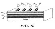
- FIG. 16is a schematic diagram showing an illustrative array of four VCSELs having a common epitaxial structure including a bottom mirror, an active region, a top mirror and a top GMGRF, where the grating period of each GMGRF is different for each VCSEL;
- FIG. 17is a schematic diagram showing an illustrative WDMIVDD application using the array of four VCSELs of FIG. 16 ;
- FIG. WDM/WDDis a schematic diagram showing an illustrative GMGRF filter in accordance with the present invention.
- FIG. 19is a graph showing the relationship between grating period ( ⁇ ) and the resonant wavelength for the GMGRF shown in FIG. 18 ;
- FIG. 20is a graph showing the relationship between the grating height 420 /core depth 418 and the resonant wavelength for the GMGRF shown in FIG. 18 .
- FIG. 1is a schematic illustration of a planar, current-guided, GaAs/AlGaAs top surface emitting vertical cavity laser 10 in accordance with the prior art.
- n-doped gallium arsenide (GaAs) substrate 14is a n-contact 12 .
- Substrate 14is doped with impurities of a first type (i.e., n type).
- An n-type mirror stack 16is formed on substrate 14 .
- Spacer 18has a bottom confinement layer 20 and a top confinement layer 24 surrounding active region 22 .
- a p-type mirror stack 26is formed on top confinement layer 24 .
- a p-metal layer 28is formed on stack 26 .
- the emission regionmay have a passivation layer 30 .
- Isolation region 29restricts the area of the current flow 27 through the active region.
- Region 29may be formed by deep H+ ion implantation. While a deep H+ implant is provided as an illustration, it is contemplated that any type of current and field confinement may be used, including for example, gain-guided, oxide-confinement, or any other means.
- the diameter “g”may be set to provide the desired active area, and thus the gain aperture of the VCSEL 10 . Further, the diameter “g” may be set by the desired resistance of the p-type mirror stack 26 , particularly through the non-conductive region 29 . Thus, non-conductive region 29 performs the gain guiding function.
- the diameter “g”is typically limited by fabrication limitations, such as lateral straggle during the implantation step.
- Spacer 18may contain a bulk or quantum-well active region disposed between mirror stacks 16 and 26 .
- Stacks 16 and 26are distributed Bragg reflector (DBR) stacks, and may include periodic layers of doped AlGaAs and aluminum arsenide (AlAs).
- DBRdistributed Bragg reflector
- the AlGaAs of stack 16is doped with the same type of impurity as substrate 14 (e.g., n type), and the AlGaAs of stack 26 is doped with the other kind of impurity (e.g., p type).
- Metal contact layers 12 and 28are ohmic contacts that allow appropriate electrical biasing of laser diode 10 .
- active region 22emits light 31 which passes through stack 26 .
- a typical near IR VCSELrequires high reflectivity (>99%).
- an all-semiconductor DBRtypically requires 20-40 mirror periods with a thickness of 2-4 ⁇ m.
- the epi-structure required for a complete VCSEL, including both top and bottom DBR mirrors surrounding an active spacer regiontypically includes over 200 layers having a thickness in excess of 7-8 ⁇ m.
- FIG. 2is a schematic cross-sectional side view of a planar, current-guided, GaAs/AlGaAs top surface emitting vertical cavity laser with a hybrid top mirror including a resonant reflector 52 and a distributed Bragg reflector 56 .
- This devicecombines the anomalous filtering properties of guided mode resonance in a dielectric waveguide grating with the reflective properties of a conventional DBR mirror.
- the hybrid mirror structureincludes, for example, a resonant reflector 52 and a DBR mirror 56 .
- the bottom mirrormay also include a resonant reflector structure, if desired.
- a dielectric resonant reflector 52is highly reflective on resonance, and may be more reflective than a corresponding DBR type mirror at the same wavelength.
- the number of DBR mirror periods needed for a given reflectancemay be reduced.
- lateral straggle effects during ion implantation of the gain guiding region 62 through the DBR mirrorsoften limits the lateral dimension 64 of the active region to ⁇ 10 ⁇ m. This directly impacts the minimum achievable threshold current, single mode operation, and indirectly impacts the speed of the VCSEL.
- a resonant reflectorinto the top mirror, equivalent or superior reflectance properties in a structure five to ten times thinner may be achieved. This may translate into an ion implant that is more controllable, which may reduce the volume of the active region.
- a smaller active regionmay reduce the operating current and power of the device, improve planarity and thus the monolithic integrability of the VCSEL with electronics and smart pixels, and may provide a controllable single mode and single polarization emission with increased modal control.
- the hybrid approach of FIG. 2is compatible with alternate existing gain-guiding techniques including etched pillars (with or without planarization and/or regrowth), lateral oxidation, selective growth, etc.
- the resonant reflectormay improve the processibility and performance of the alternate current guiding approaches. While ion implantation is provided as an illustration, it is contemplated that any type of current and field confinement may be used, including for example, gain-guided, oxide-confinement, or any other means.
- the resonant reflector 52 of FIG. 2includes a three layer waveguide-grating structure suitable for use in a near IR VCSEL.
- the three-layer stackmay be designed to function both as an anti-reflection (AR) coating near the emission wavelength for the VCSEL-structure substrate and independently as a guided-mode resonant reflector waveguide-grating (i.e. a guided-mode grating resonant reflector filter or GMGRF).
- ARanti-reflection
- GMGRFguided-mode resonant reflector waveguide-grating
- the three layers of resonant reflector 52may form an anti-reflective region, which provides little reflectance for at least a predetermined range of wavelengths including a resonant wavelength.
- the grating multilayer waveguide structure shown at 52causes the structure to become substantially more reflective, at least at the resonant wavelength.
- the three-layer stack 52may be designed to function both as a high -reflectivity coating for the VCSEL-structure substrate and independently as a guided-mode resonant reflector waveguide-grating.
- the three-layer structure 52forms a highly-reflective mirror region which provides reflectance for at least a predetermined range of wavelengths including a resonant wavelength (e.g., near 980 nm).
- the overall reflectance of the top mirror, including layers 66 and 68may be less than that required for lasing. This may be accomplished by, for example, reducing the number of mirror periods in the top DBR mirror 56 .
- Grating layer 58causes the guided mode resonant reflector structure 52 to become substantially more reflective at least near the resonant wavelength. In either case, the number of DBR mirror layers beneath the resonant reflector 52 may be reduced relative to the conventional VCSEL construction shown in FIG. 1 .
- Resonanceis achieved in the resonance reflector 52 by matching the first-diffraction order wave vector of the grating 58 to the propagating mode of the waveguide 66 . Since the latter depends on polarization, the reflectance is inherently polarization -selective.
- the resonant wavelengthis determined primarily by the grating period 60 , and the bandwidth is determined primarily by the modulation of the refractive index and fill factor of the grating 58 .
- the top layer, middle layer and bottom layerare formed from Indium Tin Oxide (ITO), GaAs, and AlGaAs, respectively.
- the refraction indices for the top, middle and bottom layersare 1.96, 3.5 and 3.24, respectively, and the thicknesses of the top, middle and bottom layers are preferably ⁇ /4, 3 ⁇ /4 and ⁇ /4, respectively.
- the layersare placed on a substrate with an effective reflective index of 3.2. This structure is simulated to exhibit one transverse Electric (TE) mode resonance (with a polarization parallel to the grating), no perpendicular resonance and a low out of resonant reflectance near 10 ⁇ 6 .
- TEtransverse Electric
- the imaginary component “k” of the refractive indexis related to optical absorption and electrical conductivity of the resonant reflector.
- the same three layers, all with k0, indicating a dielectric resonant reflector, produces theoretically 100 percent reflectance.
- This graphillustrates the extreme sensitivity of the resonant reflector 52 to absorption, or more generally, to loss of any kind.
- the conductivity of the resonant reflectorshould also be zero (e.g., non-conductive).
- the reflectance curvehas a narrow bandwidth, and reaches about 100% reflectivity at the resonant wavelength.
- the present inventioncontemplates isolating the resonant reflector from adjacent conducting layers. Isolation is preferably accomplished by providing a non-conductive (e.g. dielectric) buffer or cladding layer between the resonant reflector and the adjacent conducting layer of the optoelectronic device.
- the non-conductive cladding or buffer layeris preferably sufficiently thick, and/or has a sufficiently low refractive index relative to the refractive index of the waveguide of the resonant reflector, to substantially prevent energy in the evanescent tail of the guided mode in the waveguide from entering the adjacent conductive layer of the optoelectronic device.
- the waveguideis formed from a dielectric that has a higher refractive index than the refractive index of the buffer or cladding layer, and also higher than the average refractive index of the grating.
- the thickness of the waveguidepreferably depends on the refractive index difference between the waveguide and the buffer or cladding layer.
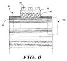
- FIG. 6is a schematic cross-sectional side view of a planar, current-guided, GaAs/AlGaAs top surface emitting vertical cavity laser with a cladding or buffer layer 80 interposed between the waveguide layer 82 of the resonant reflector 84 and the top DBR mirror 86 .
- the cladding or buffer layer 80is preferably sufficiently thick, and/or has a sufficiently low refractive index relative to the refractive index of the waveguide of the resonant reflector, to substantially prevent energy in the evanescent tail of the guided mode in the waveguide from entering an adjacent conductive layer of the optoelectronic device.
- the grating layer 90is SiO 2 with an index of refraction of about 1.484 and a thickness of 0.340 ⁇ m.
- the waveguide layer 82may be GaAs with an index of refraction of 3.523 and a thickness of 0.280 ⁇ m.
- the waveguidemay be a ternary compound such as Al x Ga 1-x As, with x close to one, or a high refractive index dielectric such as TiO2, ZrO2, HfO2, or Si3N4.
- the thickness of the waveguidepreferably depends on the refractive index difference between the waveguide and the buffer or cladding layer.
- the cladding or buffer layer 80 in the illustrative embodimentis AlO, with an index of refraction of 1.6 and a thickness of 0.766 ⁇ m.
- the top DBR mirror layer 92may be AlGaAs with an index of refraction of 3.418 and a thickness of 0.072 ⁇ m.
- the cladding or buffer layer 80has an increased thickness and a reduced index of refraction relative to the embodiment shown in FIG. 2 , both of which help prevent energy in the evanescent tail of the guided mode in the waveguide layer 82 from entering the top DBR mirror layer 92 . It is contemplated however, that similar results may be achieved by either increasing the thickness or reducing the index of refraction of the cladding or buffer layer 80 , if desired.
- the cladding or buffer layer 80may be AlO, which has a relatively low refractive index. In one method, this can be accomplished by initially forming the cladding or buffer layer 80 with AlGaAs, with a relatively high concentration of aluminum (e.g. >95%). AlGaAs has a relatively high index of refraction. Then, the waveguide layer 82 and grating layer 90 are provided. The cladding or buffer layer 80 , waveguide layer 82 and grating 90 may then be removed around the periphery of the desired optical cavity. Contacts 93 may then be deposited on the exposed top mirror 86 to provide electrical contact to the top mirror.
- the devicemay be subject to an oxidizing environment, which oxidizes the AlGaAs material of the cladding or buffer layer 80 , resulting in AlO which has a relatively low refractive index.
- the AlGaAs materialis preferably oxidized laterally in from the exposed edges of the cladding or buffer layer 80 .
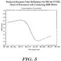
- the reflectance curvehas a narrow bandwidth (0.00975 nm), and theoretically reaches 100% reflectivity at the resonant wavelength.
- the reflectance curvestill has a narrow bandwidth (0.0097 nm), and theoretically reaches 100% reflectivity at the resonant wavelength. Therefore, and unlike FIG. 5 , there is little or no degradation in the observed reflectance of the resonant reflector, even when placed adjacent a conductive layer.
- FIG. 9is a schematic cross-sectional side view of a top surface emitting vertical cavity laser similar to that shown in FIG. 6 , but with a modified grating fill factor.
- the grating fill factoris defined as the grating spacing 102 divided by the grating period 100 .
- the resonant wavelength of a resonant reflectoris often determined by the grating period 100 , and the spectral bandwidth is often determined by the modulation of the refractive index and fill factor of the grating.
- the modulation of the refractive indexis related to the difference between the dielectric constants of the grating material and the material that fills the spaces between the grating elements, divided by the average dielectric constant across the grating.
- the average dielectric constant across the gratingcan be changed by varying the fill factor of the grating. For example, and assuming a constant grating period, the grating fill factor can be increased by reducing the width of each grating element.
- a limitation of achieving a desired spectral bandwidth of a resonant reflector by altering the grating fill factoris that the design rules of many manufacturing processes limit the minimum width of the grating elements.
- FIG. 10is a schematic cross-sectional side view of a top surface emitting vertical cavity laser similar to that shown in FIG. 6 , but with a grating film that has a controlled etch depth to control the spectral bandwidth of the resonant reflector.
- a grating film 120is provided and subsequently etched to form two or more spaced grating regions 122 a - 122 c separated by one or more spaced etched regions 124 a - 124 b .
- the depth of the etchis controlled.
- a desired average dielectric constant across the gratingcan be achieved.
- the grating width and grating spacingmay be optimized to the design rules of the manufacturing process, and the etch depth can be controlled to achieve the desired spectral bandwidth. For example, a fill factor of about 50% is preferred. This may increase the producibility and yield of the resonant reflector.
- FIG. 11is a schematic cross-sectional side view of a vertical cavity surface emitting laser that is formed by bonding a resonant reflector 132 that is prepared on a first substrate 130 to a top mirror 134 of a vertical cavity surface emitting laser that is prepared on a second substrate.
- a resonant reflectoris formed on a front side 131 of a first substrate 130 . This includes forming at least a waveguide 136 and a grating 138 , as shown.
- an optoelectronic devicesuch as a vertical cavity surface emitting laser or resonant cavity photodetector, is prepared on a front side of a second substrate. In FIG. 11 , this includes a bottom DBR mirror, an active region, a top DBR mirror 134 , and one or more contacts 140 .
- the front side of the first substrate 130is bonded to the front side of the second substrate to complete the optoelectronic device.
- the first substrate 130may be bonded to the second substrate using an optical epoxy 144 , and preferably a non-conductive optical epoxy.
- the optical epoxyis preferably sufficiently thick, or has a sufficiently low refractive index relative to the refractive index of the waveguide 136 of the resonant reflector 132 , so that the energy from the evanescent wave vector in the waveguide 136 is substantially prevented from entering the optoelectronic device on the first substrate.
- a anti-reflective coating 148may be applied to the backside of the first substrate 130 as shown.
- the relative position of the waveguide 136 and grating 138may be changed.
- the gratingmay be positioned more toward the front side of the first substrate than the waveguide.
- the waveguidemay be positioned more toward the front side of the first substrate than the grating, if desired.
- FIG. 12is a schematic cross-sectional side view of the vertical cavity surface-emitting laser of FIG. 11 with a microlens 150 positioned on the backside of the first substrate 130 .
- a microlenssuch as a collimating microlens may be formed on the backside of the first substrate 130 .
- a collimating microlensmay be formed on the backside of the substrate that carries the bottom mirror, the active region and the top mirror of the optoelectronic device. In either case, the collimating microlens 150 is preferably placed in registration with the output of the optoelectronic device as shown.
- a number of optoelectronic devicesmay be formed on a common substrate, as shown in FIG. 13 .
- One application for such a configurationis a monolithic transceiver that includes one or more light emitting devices 190 and one or more light receiving devices 192 and 194 .
- both the light emitting and light receiving devicesare formed on a common substrate (not shown).
- a bottom mirroris first formed on the common substrate. The bottom mirror may serve as the bottom mirror for more than one of the optoelectronic devices 190 , 192 and 194 , and is preferably a DBR mirror stack that is doped to be at least partially conductive.
- An active region 200is then formed on the bottom mirror, followed by a top mirror 202 .
- the top mirror 202is preferably a DBR mirror stack, and is doped to be the opposite conductivity type of the bottom mirror.
- the active region 200may include cladding layers 204 on either side of the active region 200 to help focus the light energy and current in the active region.
- a deep H+ ion implantmay provide gain guide apertures for selected optoelectronic devices, and may further electrically isolate adjacent devices from one another. While a deep H+ implant is provided as an illustration, it is contemplated that any type of current and field confinement may be used, including for example, gain-guided, oxide-confinement, or any other means. Contacts 208 a - 208 d may be provided on the top mirror 202 and on the bottom surface of the common substrate to provide electrical contact to each of the optoelectronic devices.
- a cladding or buffer layer 210may be provided above the top mirror 202 .
- a resonant reflectormay then be provided on top of the cladding or buffer layer 210 .
- the resonant reflectormay include a waveguide 212 and a grating film 214 .
- the grating film 214may be etched to form a grating, as shown. The grating may substantially increase the reflectivity of the resonant reflector in those regions.
- the grating filmmay either include a different grating structure (e.g., wider spectral bandwidth), or remain non-etched as shown.
- the grating filmmay be removed altogether, and a metal grid 214 a - 214 c may be formed on the waveguide layer 212 or cladding or buffer layer 210 , as desired.
- MSMMetal-Semiconductor-Metal
- the cladding or buffer layer 210may be sufficiently thick to substantially prevent energy in the evanescent tail of the guided mode in the waveguide 212 from entering the top mirror 202 .
- the cladding or buffer layer 210may be formed from a material that has a sufficiently low refractive index relative to the refractive index of the waveguide 212 to substantially prevent energy in the evanescent tail of the guided mode in the waveguide 212 from entering the top mirror 202 .
- resonant reflector optoelectronic structureswill permit polarization, emission wavelength and mode control. These structures and properties can be designed and fabricated using techniques such as lithography or holography, and may not be subject to growth thickness variations alone. The above techniques can be applied to produce, for example, VCSELs with high power single-mode/polarization emission from apertures exceeding a few microns in diameter. Furthermore, wavelength and/or polarization variation across a chip, array or wafer can be used for spatially varied wavelength/polarization division multiplexing, multi-wavelength spectroscopy, etc.
- FIG. 14is a schematic diagram of a number of illustrative optoelectronic emitters that have a guided-mode resonant reflector waveguide-grating (i.e. a guided-mode grating resonant reflector filter or GMGRF) for data/telecommunication, processing, switching, etc., including embodiments conducive for wavelength division multiplexing, polarization division multiplexing, space division multiplexing, etc.
- the illustrative optoelectronic emittersare shown at 300 , 302 , 304 and 306 , respectively, and in the illustrative embodiment are monolithically formed on a common substrate 308 .
- Each optoelectronic emitterincludes a GMRGF filter integrated with or adjacent to the top mirror of the emitter.
- the optoelectronic emittersare VCSEL devices.
- the GMGRF of each emitterincludes a waveguide and a grating.
- the various gratingsare shown using parallel lines in FIG. 14 , with each grating having different characteristics.
- a first optoelectronic emitter 300includes a grating that extends in a horizontal direction and has a first grating period.
- the grating directionhelps determine the polarization direction of the light that is resonantly reflected by the GMGRF.
- the grating periodmay help determine the resonant wavelength of the GMGRF.
- the output emissionmay be inherently wavelength selective.
- a second optoelectronic emitteris shown at 302 .
- Optoelectronic emitter 302includes a grating that also extends in a horizontal direction, but has a second grating period.
- the second optoelectronic emitter 302may produce light that is polarized in the same direction as the first optoelectronic emitter 300 .
- the narrower grating periodmay produce a shorter wavelength than the first optoelectronic emitter 300 .
- a third optoelectronic emitteris shown at 304 .
- Optoelectronic emitter 304includes a grating that also extends in a horizontal direction, but has a third grating period.
- the third optoelectronic emitter 304produces light that is polarized in the same direction as the first and second optoelectronic emitters.
- the larger grating periodmay produce a longer wavelength than the first and second optoelectronic emitters.
- Optoelectronic emitter 306includes a grating that also extends in a perpendicular direction to that of the other optoelectronic emitters 300 , 302 and 304 .
- the fourth optoelectronic emitter 306produces light that is polarized in a direction that is perpendicular to that of the other optoelectronic emitters 300 , 302 and 304 .
- the period and/or direction of the gratingmay allow designers to control lithographically both the operating wavelength and polarization direction of the corresponding optoelectronic emitter devices. This may allow for SDM/WDM/PDM architectures having distributed wavelength and polarization modes. If the admission of light having any polarization is desired, the GMGRF may be fabricated with two crossed gratings aligned orthogonally with each other (e.g. bi-gratings).
- the use of a GMGRF reflectorcan reduce the number of top DBR mirror periods when compared to an all-epitaxial DBR VCSEL or RCPD device. Reducing the number of DBR mirror periods can reduce the overall thickness of the device, which can lead to greater amenability to integration. Increased planarity and the utilization of standard semiconductor planar batch fabrication processes may also help improve producibility. The capability to readily control the wavelength, angular and bandwidth properties of the GMGRF reflector can provide greater flexibility in the construction of multi-element integrated circuits.
- FIG. 15is a graph showing reflectance versus wavelength for the three GMRGF filters 300 , 302 and 304 of FIG. 14 .
- Curves 310 , 312 and 314correspond to the GMGRF reflectance versus wavelength for optoelectronic devices 300 , 302 and 304 , respectively.
- the grating period ( ⁇ ) of the first optoelectronic device 300is 480 nm, which in the example shown, results in a peak reflectance at a wavelength of about 843 nm.
- the grating period ( ⁇ ) of the second optoelectronic device 302is 460 nm, which in the example shown, results in a peak reflectance at a wavelength of about 811 nm.
- the grating period ( ⁇ ) of the third optoelectronic device 304is 500 nm, which in the example shown, results in a peak reflectance at a wavelength of about 882 nm.
- the reflectance versus wavelength of the fourth optoelectronic device 306is not shown in FIG. 15 .
- the number of DBR mirror periods of the top mirror of a VCSEL or RCPD devicemay be reduced, preferably so that resonance cannot readily be established without the additional reflectance provided by the GMGRF.
- the reflectance provided the GMGRFvaries from near zero to near 100%, depending on the wavelength. Therefore, unique wavelength and/or polarization selectively may be provided for each optoelectronic device 300 , 302 , 304 and 306 by selecting appropriate parameters for the corresponding GMGRF.
- the resonant wavelength of the GMGRFmay help determine, to a large extent, the cavity resonance wavelength and/or polarization of the corresponding optoelectronic device.
- FIG. 16is a schematic diagram showing an illustrative array of four VCSEL devices 320 , 322 , 324 and 326 fabricated as a common epitaxial structure.
- the common epitaxial structureincludes a bottom mirror 330 , an active region 332 , and a top mirror 334 .
- a top GMGRFis integrated with or provided adjacent to the top mirror 334 , and in the embodiment shown, the grating period ( ⁇ ) of each GMGRF is different for each VCSEL device.
- the number of top DBR mirror periodsis less than the number of bottom DBR mirror periods.
- the number of top DBR mirror periodsis preferably reduced so that the lasing threshold cannot readily be established without the additional reflectance provided by the corresponding GMGRF.
- the VCSEL devices 320 , 322 , 324 and 326may be processed with topside electrical contacts with the GMGRF films positioned in the emitting aperture of each VCSEL.
- a 1 nm increase in the grating period ( ⁇ )may yield about a 1.8 nm increase in the resonant wavelength.
- the grating periods for the four VCSEL devices 320 , 322 , 324 and 326may be approximately 477.2 nm, 480 nm, 482.8 nm, and 485.8 nm.
- FIG. 17is a schematic diagram showing an illustrative WDM/WDD/PDM application using the array of VCSEL devices of FIG. 16 .
- Optical Emitter-A 350corresponds to VCSEL 320 , which produces a first wavelength ⁇ 1 as shown at 351 .
- Optical Emitter-B 352corresponds to VCSEL 322 , which produces a second wavelength ⁇ 2 as shown at 353 .
- Optical Emitter-C 354corresponds to VCSEL 324 , which produces a third wavelength ⁇ 3 as shown at 355 .
- Optical Emitter-D 356corresponds to VCSEL 326 , which produces a fourth wavelength ⁇ 4 as shown at 357 .
- the various wavelengths 351 , 353 , 355 and 357are provided to a common optical receiver element by block 360 .
- the common optical receiver elementmay be, for example, a common optical fiber 362 , as shown.
- PDMpolarization Division Multiplexing
- one or more optoelectronic receivers 370 , 372 , 374 and 376are provided.
- the light transmitted by the optical fiber 362is provided to each of the optoelectronic receivers 370 , 372 , 374 and 376 .
- Each of the optoelectronic receivers 370 , 372 , 374 and 376may be tuned to select the wavelength of one (or more) of the optical data channels.
- each of the optoelectronic receives 370 , 372 , 374 and 376is a RCPD device, with a GMGRF resonator that is tuned to a wavelength of a desired optical data channel.
- Each RCPDmay be similar to the VCSEL devices 320 , 322 , 324 and 326 discussed above with respect to FIG. 16 , but may be operated in a reverse bias mode.
- the effective reflectivity of the top mirrormay be reduced and the lateral dimensions of the resonant cavity may be increased relative to a VCSEL device, which may increase the amount of light that is allowed to enter by the optical cavity.
- selected wavelengthsmay be directed to an optical receiver by an optical filter, optical splitter, or the like.
- the optical receivermay be a wide band optical receiver, as the wavelength selectivity is provided by the optical filter, optical splitter, or the like, rather than the optical receiver itself.
- FIG. 18is a schematic diagram showing an illustrative GMGRF filter 400 in accordance with the present invention.
- the GMGRF filter 400may be incorporated into or positioned adjacent the top and/or bottom mirror of a VCSEL or RCPD device.
- the resonant wavelength of the GMGRF 400may determine, at least to a large extent, the cavity resonance of the VCSEL or RCPD device.
- the GMGRF 400includes a buffer layer 402 interposed between a core layer 404 and the top DBR mirror layer 406 .
- the buffer layer 402also serves as a clad layer.
- the buffer layer 402is preferably sufficiently thick, and/or has a sufficiently low refractive index relative to the refractive index of the core layer 404 of the resonant reflector, to substantially prevent energy in the evanescent tail of the guided mode in the core layer 404 from entering an adjacent conductive layer of the optoelectronic device.
- an upper clad layer 410is provided over a grating etched into the core layer 404 .
- the grating elements 412 of the gratingpreferably have a grating period 414
- the core layer 404preferably has a core depth 418 between adjacent grating elements 412 .
- the overall core thickness at the grating elements 412is shown at 416 .
- the core layer 404is TiO2 with an index of refraction of about 2.41, and has a core depth of about 0.175 ⁇ m.
- the core layer 404may be, for example, GaAs or some other relatively high refractive index dielectric such as ZrO2, HfO2, or Si3N4.
- the thickness of the core layer 404preferably is dependent on the refractive index difference between the core layer 404 and the buffer layer 402 .
- the upper clad layer 410is SiO 2 with an index of refraction of about 1.48, and having a clad depth 417 of about 0.285 ⁇ m.
- the upper clad layer 410extends down between the grating elements 412 of the core layer 404 , as shown.
- the upper clad layer 410has an overall clad layer thickness between grating elements 412 that equals the clad depth 417 plus the grating height 420 , or in this case about 0.495 ⁇ m.
- the buffer layer 402 in the illustrative embodimentis SiO2, with an index of refraction of 1.48 and a thickness of 0.285 ⁇ m.
- the top layer of the DBR mirror 406may be, for example, AlGaAs with an index of refraction of 3.2.
- the buffer layer 402preferably has an increased thickness and/or a reduced index of refraction, both of which help prevent energy in the evanescent tail of the guided mode in the core layer 404 from entering the top DBR mirror 406 .
- the resonant wavelength of the GMGRF 400can be set in a reliable manner by appropriately selecting GMGRF parameters, such as the grating period ( ⁇ ) 414 , core depth 418 versus grating height 420 , grating direction, etc. More specifically, and in one illustrative embodiment, in an array of VCSEL devices having a common epitaxial structure (bottom mirror, active region, top mirror including a GMGRF), the lasing wavelength of each VCSEL in the array can be prescribed individually by changing the GMGRF parameters that affect the resonant wavelength.
- GMGRF parameterssuch as the grating period ( ⁇ ) 414 , core depth 418 versus grating height 420 , grating direction, etc.
- thiscan be done by changing the grating period ( ⁇ ) 414 while keeping all other parameters fixed, or by increasing the grating height 420 while maintaining a substantially constant core thickness 416 (and hence reducing the core depth 418 of the core layer 404 by a corresponding amount), while keeping the grating period ( ⁇ ) 414 fixed.
- these and/or other GMGRF parametersmaybe changed in any suitable manner to achieve the desired resonant wavelength for each VCSEL in the array.
- FIG. 19is a graph showing the relationship between the grating period ( ⁇ ) 414 and the resonant wavelength for the GMGRF shown in FIG. 18 .
- the DBR epilayers in the top mirror of a VCSELare represented as a single layer having an average refractive index of 3.2.
- the upper clad layer 410 and buffer layer 402have optical thicknesses of a half-wave at approximately 850 nm (about 0.285 ⁇ m).
- the grating elements 412provide modulation in the dielectric constant of the core layer 404 , and enforces coupling of a normally-incident planewave via the first diffractive order of the grating into a guided-mode supported by the core layer 404 .
- a desired resonant wavelength ⁇ 1 and polarizationare then selected.
- the film thicknessesare preferably chosen on the basis of out-of-band optical reflectance, throughput, and core isolation from the substrate.
- the gratingmay be modeled as its homogenized equivalent thin film, and the structure may be analyzed as a multi-layer planar waveguide. This analysis may yield the guided mode eigenvalues ⁇ for the waveguide, and one (usually the fundamental mode with largest ⁇ ) is chosen. The grating period which excites this mode is then given approximately by equation (1) above. Illustrated results for the GMGRF 400 of FIG. 18 are shown graphically in FIG. 19 .
- FIG. 20is a graph showing the relationship between the grating height 420 /core depth 418 and the resonant wavelength for the GMGRF shown in FIG. 18 .
- the resonant wavelength of the GMGRF 400may be controlled by increasing the grating height 420 while maintaining a substantially constant core thickness 416 (and hence reducing the core depth 418 of the core layer 404 by a corresponding amount), while keeping the grating period ( ⁇ ) 414 fixed.
- Illustrated results for the GMGRF 400 of FIG. 18are shown graphically in FIG. 20 for four combinations of grating height 420 and core depth 418 , while leaving the overall core thickness 416 and grating period 414 constant.
- the structurecan be analyzed with a grating solver to estimate more precisely the GMGRF resonant wavelength and the Fabry-Perot resonance of the combined top-mirror assembly with the rest of the VCSEL or RCPD structure. If desired, minor adjustments in the GMGRF parameters can then be made to yield a desired resonant wavelength.
- wavelength selectivity capability of such GMGRF filtershas applicability in display applications.
- the grating itselfmay determine the wavelength of operation, and fabrication is done lithographically, laterally-displaced wavelength dependent emitters can be formed.
- Such a structuremay also serve as a quasi-tunable laser source.
- Wavelength tunable VCSELs and detectors, as described above,may also find use in spectroscopic and sensing applications.
- the improved performance coupled with the capability to control polarizationcan also lend itself to applications in polarization-sensitive optical read/write applications. Included are various forms of CD, DVD, and holographic storage applications. Laser printing heads may also benefit.
- the performance advantage, and use of thinner top and/or bottom mirrorsbecomes even more paramount when extending VCSELs into the visible wavelengths, where typical all-epitaxial DBRs become prohibitively thick and may require twice as many layers.
Landscapes
- Physics & Mathematics (AREA)
- Condensed Matter Physics & Semiconductors (AREA)
- General Physics & Mathematics (AREA)
- Electromagnetism (AREA)
- Optics & Photonics (AREA)
- Semiconductor Lasers (AREA)
Abstract
Description
β=2π/Λ Equation (1)
where Λ is the
<n>2=FF*nhi2+(1−FF)*nlo2for TE polarization Equation (2)
OR
<n>−2=FF*nhi−2+(1−FF)*nlo2for TM polarization Equation (3)
where FF equals the grating fill factor defined with respect to the high index material.
Claims (21)
Priority Applications (1)
| Application Number | Priority Date | Filing Date | Title |
|---|---|---|---|
| US10/948,870US8599897B2 (en) | 2000-12-29 | 2004-09-23 | Tunable detector |
Applications Claiming Priority (3)
| Application Number | Priority Date | Filing Date | Title |
|---|---|---|---|
| US09/751,422US6782027B2 (en) | 2000-12-29 | 2000-12-29 | Resonant reflector for use with optoelectronic devices |
| US10/121,490US6836501B2 (en) | 2000-12-29 | 2002-04-12 | Resonant reflector for increased wavelength and polarization control |
| US10/948,870US8599897B2 (en) | 2000-12-29 | 2004-09-23 | Tunable detector |
Related Parent Applications (1)
| Application Number | Title | Priority Date | Filing Date |
|---|---|---|---|
| US10/121,490ContinuationUS6836501B2 (en) | 2000-12-29 | 2002-04-12 | Resonant reflector for increased wavelength and polarization control |
Publications (2)
| Publication Number | Publication Date |
|---|---|
| US20050036533A1 US20050036533A1 (en) | 2005-02-17 |
| US8599897B2true US8599897B2 (en) | 2013-12-03 |
Family
ID=34138152
Family Applications (1)
| Application Number | Title | Priority Date | Filing Date |
|---|---|---|---|
| US10/948,870Active2028-06-12US8599897B2 (en) | 2000-12-29 | 2004-09-23 | Tunable detector |
Country Status (2)
| Country | Link |
|---|---|
| US (1) | US8599897B2 (en) |
| TW (1) | TWI227799B (en) |
Cited By (3)
| Publication number | Priority date | Publication date | Assignee | Title |
|---|---|---|---|---|
| US9755097B2 (en)* | 2015-03-20 | 2017-09-05 | Kabushiki Kaisha Toshiba | Semiconductor photoreceiving device |
| US10084285B1 (en) | 2017-08-28 | 2018-09-25 | Hewlett Packard Enterprise Development Lp | Orthoganolly polarized VCSELs |
| US10177872B1 (en) | 2017-09-25 | 2019-01-08 | Hewlett Packard Enterprise Development Lp | Orthogonally polarized VCSELs |
Families Citing this family (13)
| Publication number | Priority date | Publication date | Assignee | Title |
|---|---|---|---|---|
| KR100810312B1 (en)* | 2006-02-07 | 2008-03-04 | 삼성전자주식회사 | Multichannel Bidirectional Optical Transceiver |
| CN103201969B (en) | 2010-10-08 | 2016-10-19 | 慧与发展有限责任合伙企业 | Optical multiplexing using laser arrays |
| CN103250080B (en) | 2010-10-08 | 2016-04-13 | 惠普发展公司,有限责任合伙企业 | Use the light polarization of laser array multiplexed |
| MX361240B (en)* | 2013-12-18 | 2018-11-30 | Halliburton Energy Services Inc | Optical computing device having detector with non-planar semiconductor structure. |
| US20200006924A1 (en)* | 2016-12-05 | 2020-01-02 | Goertek, Inc. | Micro Laser Diode Display Device and Electronics Apparatus |
| US10971890B2 (en)* | 2016-12-05 | 2021-04-06 | Goertek, Inc. | Micro laser diode transfer method and manufacturing method |
| US10928569B2 (en)* | 2018-04-24 | 2021-02-23 | Palo Alto Research Center Incorporated | Angle-insensitive multi-wavelength optical filters with hue control |
| US11125689B2 (en)* | 2018-07-13 | 2021-09-21 | The Government Of The United States Of America, As Represented By The Secretary Of The Navy | Highly stable semiconductor lasers and sensors for III-V and silicon photonic integrated circuits |
| CN113193091B (en)* | 2020-04-14 | 2022-05-31 | 镭昱光电科技(苏州)有限公司 | Light emitting diode structure with resonant cavity and manufacturing method thereof |
| CN113488846B (en)* | 2021-07-14 | 2024-05-07 | 中国科学院半导体研究所 | Sub-wavelength grating and vertical cavity surface emitting laser |
| CN115528530A (en)* | 2022-08-11 | 2022-12-27 | 深圳市德明利光电有限公司 | Laser emission assembly and data acquisition device |
| US20240186766A1 (en)* | 2022-10-19 | 2024-06-06 | Ii-Vi Delaware, Inc. | Polarized/lensed back-side emitting (bse) vertical-cavity surface-emitting laser (vcsel) |
| CN119447993B (en)* | 2025-01-09 | 2025-04-15 | 无锡市华辰芯光半导体科技有限公司 | Edge-emitting laser sensing chip and preparation method thereof |
Citations (95)
| Publication number | Priority date | Publication date | Assignee | Title |
|---|---|---|---|---|
| US4317085A (en) | 1979-09-12 | 1982-02-23 | Xerox Corporation | Channeled mesa laser |
| US4466694A (en) | 1978-06-15 | 1984-08-21 | Her Majesty The Queen In Right Of Canada, As Represented By The Minister Of National Defence Of Her Majesty's Canadian Government | Wavelength selective optical coupler |
| JPS60123084A (en) | 1983-12-08 | 1985-07-01 | Matsushita Electric Ind Co Ltd | semiconductor light generator |
| US4660207A (en) | 1984-11-21 | 1987-04-21 | Northern Telecom Limited | Surface-emitting light emitting device |
| EP0288184A2 (en) | 1987-04-21 | 1988-10-26 | Gec-Marconi Limited | Semiconductor diode laser array |
| US4784722A (en) | 1985-01-22 | 1988-11-15 | Massachusetts Institute Of Technology | Method forming surface emitting diode laser |
| US4885592A (en) | 1987-12-28 | 1989-12-05 | Kofol J Stephen | Electronically steerable antenna |
| US4901327A (en) | 1988-10-24 | 1990-02-13 | General Dynamics Corporation, Electronics Division | Transverse injection surface emitting laser |
| JPH0254981A (en) | 1988-08-20 | 1990-02-23 | Fujitsu Ltd | Surface emitting laser and laser array |
| US4904045A (en) | 1988-03-25 | 1990-02-27 | American Telephone And Telegraph Company | Grating coupler with monolithically integrated quantum well index modulator |
| US4943970A (en) | 1988-10-24 | 1990-07-24 | General Dynamics Corporation, Electronics Division | Surface emitting laser |
| US4956844A (en) | 1989-03-17 | 1990-09-11 | Massachusetts Institute Of Technology | Two-dimensional surface-emitting laser array |
| US5031187A (en) | 1990-02-14 | 1991-07-09 | Bell Communications Research, Inc. | Planar array of vertical-cavity, surface-emitting lasers |
| US5052016A (en) | 1990-05-18 | 1991-09-24 | University Of New Mexico | Resonant-periodic-gain distributed-feedback surface-emitting semiconductor laser |
| US5056098A (en) | 1990-07-05 | 1991-10-08 | At&T Bell Laboratories | Vertical cavity laser with mirror having controllable reflectivity |
| US5062115A (en) | 1990-12-28 | 1991-10-29 | Xerox Corporation | High density, independently addressable, surface emitting semiconductor laser/light emitting diode arrays |
| US5068869A (en) | 1987-06-19 | 1991-11-26 | Lockheed Missiles & Space Company, Inc. | Surface-emitting laser diode |
| US5079774A (en) | 1990-12-27 | 1992-01-07 | International Business Machines Corporation | Polarization-tunable optoelectronic devices |
| US5115442A (en) | 1990-04-13 | 1992-05-19 | At&T Bell Laboratories | Top-emitting surface emitting laser structures |
| US5117469A (en) | 1991-02-01 | 1992-05-26 | Bell Communications Research, Inc. | Polarization-dependent and polarization-diversified opto-electronic devices using a strained quantum well |
| US5140605A (en) | 1991-06-27 | 1992-08-18 | Xerox Corporation | Thermally stabilized diode laser structure |
| US5157537A (en) | 1991-02-01 | 1992-10-20 | Yeda Research And Development Co., Ltd. | Distributed resonant cavity light beam modulator |
| US5158908A (en) | 1990-08-31 | 1992-10-27 | At&T Bell Laboratories | Distributed bragg reflectors and devices incorporating same |
| US5216680A (en) | 1991-07-11 | 1993-06-01 | Board Of Regents, The University Of Texas System | Optical guided-mode resonance filter |
| US5216263A (en) | 1990-11-29 | 1993-06-01 | Xerox Corporation | High density, independently addressable, surface emitting semiconductor laser-light emitting diode arrays |
| US5237581A (en) | 1990-11-14 | 1993-08-17 | Nec Corporation | Semiconductor multilayer reflector and light emitting device with the same |
| US5245622A (en) | 1992-05-07 | 1993-09-14 | Bandgap Technology Corporation | Vertical-cavity surface-emitting lasers with intra-cavity structures |
| US5258990A (en) | 1991-11-07 | 1993-11-02 | The United States Of America As Represented By The Secretary Of The United States Department Of Energy | Visible light surface emitting semiconductor laser |
| JPH05299779A (en) | 1992-04-22 | 1993-11-12 | Seiko Epson Corp | Surface light emitting type semiconductor laser |
| US5285466A (en) | 1992-05-20 | 1994-02-08 | Wisconsin Alumni Research Foundation | Feedback mechanism for vertical cavity surface emitting lasers |
| US5293392A (en) | 1992-07-31 | 1994-03-08 | Motorola, Inc. | Top emitting VCSEL with etch stop layer |
| US5317587A (en) | 1992-08-06 | 1994-05-31 | Motorola, Inc. | VCSEL with separate control of current distribution and optical mode |
| DE4240706A1 (en) | 1992-12-03 | 1994-06-09 | Siemens Ag | Surface emitting laser diode |
| US5325386A (en) | 1992-04-21 | 1994-06-28 | Bandgap Technology Corporation | Vertical-cavity surface emitting laser assay display system |
| US5331654A (en) | 1993-03-05 | 1994-07-19 | Photonics Research Incorporated | Polarized surface-emitting laser |
| US5337183A (en) | 1991-02-01 | 1994-08-09 | Yeda Research And Development Co. Ltd. | Distributed resonant cavity light beam modulator |
| US5349599A (en) | 1990-03-29 | 1994-09-20 | Larkins Eric C | Bistable optical laser based on a heterostructure PNPN thyristor |
| US5351256A (en) | 1993-04-28 | 1994-09-27 | The United States Of America As Represented By The United States Department Of Energy | Electrically injected visible vertical cavity surface emitting laser diodes |
| US5359447A (en) | 1993-06-25 | 1994-10-25 | Hewlett-Packard Company | Optical communication with vertical-cavity surface-emitting laser operating in multiple transverse modes |
| US5359618A (en) | 1993-06-01 | 1994-10-25 | Motorola, Inc. | High efficiency VCSEL and method of fabrication |
| US5363397A (en) | 1992-10-29 | 1994-11-08 | Internatioal Business Machines Corporation | Integrated short cavity laser with bragg mirrors |
| US5373520A (en) | 1992-08-12 | 1994-12-13 | Fujitsu Limited | Surface emitting laser and method of manufacturing the same |
| US5386426A (en) | 1992-09-10 | 1995-01-31 | Hughes Aircraft Company | Narrow bandwidth laser array system |
| US5390209A (en) | 1994-01-05 | 1995-02-14 | At&T Corp. | Article comprising a semiconductor laser that is non-degenerate with regard to polarization |
| US5396508A (en) | 1992-09-22 | 1995-03-07 | Xerox Corporation | Polarization switchable quantum well laser |
| US5404373A (en) | 1991-11-08 | 1995-04-04 | University Of New Mexico | Electro-optical device |
| US5412680A (en) | 1994-03-18 | 1995-05-02 | Photonics Research Incorporated | Linear polarization of semiconductor laser |
| US5412678A (en) | 1992-09-22 | 1995-05-02 | Xerox Corporation | Multi-beam, orthogonally-polarized emitting monolithic quantum well lasers |
| US5416044A (en) | 1993-03-12 | 1995-05-16 | Matsushita Electric Industrial Co., Ltd. | Method for producing a surface-emitting laser |
| US5428634A (en) | 1992-11-05 | 1995-06-27 | The United States Of America As Represented By The United States Department Of Energy | Visible light emitting vertical cavity surface emitting lasers |
| US5438584A (en) | 1992-09-22 | 1995-08-01 | Xerox Corporation | Dual polarization laser diode with quaternary material system |
| US5446754A (en) | 1993-11-05 | 1995-08-29 | Photonics Research Incorporated | Phased array semiconductor laser |
| US5465263A (en) | 1992-12-12 | 1995-11-07 | Xerox Corporation | Monolithic, multiple wavelength, dual polarization laser diode arrays |
| US5475701A (en) | 1993-12-29 | 1995-12-12 | Honeywell Inc. | Integrated laser power monitor |
| US5497390A (en) | 1992-01-31 | 1996-03-05 | Nippon Telegraph And Telephone Corporation | Polarization mode switching semiconductor laser apparatus |
| US5513202A (en) | 1994-02-25 | 1996-04-30 | Matsushita Electric Industrial Co., Ltd. | Vertical-cavity surface-emitting semiconductor laser |
| US5530715A (en) | 1994-11-29 | 1996-06-25 | Motorola, Inc. | Vertical cavity surface emitting laser having continuous grading |
| US5557626A (en) | 1994-06-15 | 1996-09-17 | Motorola | Patterned mirror VCSEL with adjustable selective etch region |
| US5561683A (en) | 1994-01-27 | 1996-10-01 | Kwon; O'dae | Circular grating surface emitting laser diode |
| US5568499A (en) | 1995-04-07 | 1996-10-22 | Sandia Corporation | Optical device with low electrical and thermal resistance bragg reflectors |
| US5586131A (en) | 1993-12-10 | 1996-12-17 | Canon Kabushiki Kaisha | Oscillation polarization mode selective semiconductor laser, light source apparatus and optical communication system using the laser |
| US5590145A (en) | 1994-02-23 | 1996-12-31 | Canon Kabushiki Kaisha | Light-emitting apparatus capable of selecting polarization direction, optical communication system, and polarization modulation control method |
| US5598300A (en) | 1995-06-05 | 1997-01-28 | Board Of Regents, The University Of Texas System | Efficient bandpass reflection and transmission filters with low sidebands based on guided-mode resonance effects |
| US5606572A (en) | 1994-03-24 | 1997-02-25 | Vixel Corporation | Integration of laser with photodiode for feedback control |
| US5625729A (en) | 1994-08-12 | 1997-04-29 | Brown; Thomas G. | Optoelectronic device for coupling between an external optical wave and a local optical wave for optical modulators and detectors |
| EP0776076A1 (en) | 1995-11-21 | 1997-05-28 | Thomson-Csf | Optoelectronic quantum well device |
| US5645462A (en) | 1991-10-08 | 1997-07-08 | Canon Kabushiki Kaisha | Electron-emitting device, and electron beam-generating apparatus and image-forming apparatus employing the device |
| US5646978A (en) | 1995-04-27 | 1997-07-08 | Lucent Technologies Inc. | Method and apparatus for providing interswitch handover in personal communication services systems |
| US5648978A (en) | 1995-01-04 | 1997-07-15 | Canon Kabushiki Kaisha | Oscillation polarization mode selective semiconductor laser, modulation method therefor and optical communication system using the same |
| US5673284A (en) | 1994-05-25 | 1997-09-30 | Texas Instruments Incorporated | Integrated laser and coupled waveguide |
| US5699373A (en) | 1994-03-17 | 1997-12-16 | Canon Kabushiki Kaisha | Oscillation polarization selective semiconductor laser and optical communication system using the same |
| US5712188A (en) | 1995-12-21 | 1998-01-27 | Electronics And Telecommunications Research Institute | Fabrication method of polarization-controlled surface-emitting laser diode using tilted-cavity |
| US5727014A (en) | 1995-10-31 | 1998-03-10 | Hewlett-Packard Company | Vertical-cavity surface-emitting laser generating light with a defined direction of polarization |
| US5726805A (en) | 1996-06-25 | 1998-03-10 | Sandia Corporation | Optical filter including a sub-wavelength periodic structure and method of making |
| US5727013A (en) | 1995-10-27 | 1998-03-10 | Wisconsin Alumni Research Foundation | Single lobe surface emitting complex coupled distributed feedback semiconductor laser |
| US5774487A (en) | 1996-10-16 | 1998-06-30 | Honeywell Inc. | Filamented multi-wavelength vertical-cavity surface emitting laser |
| US5778018A (en) | 1994-10-13 | 1998-07-07 | Nec Corporation | VCSELs (vertical-cavity surface emitting lasers) and VCSEL-based devices |
| US5784399A (en) | 1996-12-19 | 1998-07-21 | Xerox Corporation | Polarization mode selection by distributed Bragg reflector in a quantum well laser |
| US5828684A (en) | 1995-12-29 | 1998-10-27 | Xerox Corporation | Dual polarization quantum well laser in the 200 to 600 nanometers range |
| US5835521A (en) | 1997-02-10 | 1998-11-10 | Motorola, Inc. | Long wavelength light emitting vertical cavity surface emitting laser and method of fabrication |
| WO1998057402A1 (en) | 1997-06-11 | 1998-12-17 | Honeywell Inc. | Resonant reflector for improved optoelectronic device performance and enhanced applicability |
| US5901166A (en) | 1994-02-18 | 1999-05-04 | Canon Kabushiki Kaisha | Oscillation polarization mode selective semiconductor laser, light transmitter and optical communication system using the laser |
| US5903590A (en) | 1996-05-20 | 1999-05-11 | Sandia Corporation | Vertical-cavity surface-emitting laser device |
| US5940422A (en) | 1996-06-28 | 1999-08-17 | Honeywell Inc. | Laser with an improved mode control |
| US5953362A (en) | 1997-12-15 | 1999-09-14 | Pamulapati; Jagadeesh | Strain induce control of polarization states in vertical cavity surface emitting lasers and method of making same |
| US5978401A (en) | 1995-10-25 | 1999-11-02 | Honeywell Inc. | Monolithic vertical cavity surface emitting laser and resonant cavity photodetector transceiver |
| US5995531A (en) | 1997-11-04 | 1999-11-30 | Motorola, Inc. | VCSEL having polarization control and method of making same |
| US6002705A (en) | 1997-12-03 | 1999-12-14 | Xerox Corporation | Wavelength and polarization multiplexed vertical cavity surface emitting lasers |
| US6008675A (en) | 1996-07-31 | 1999-12-28 | Canon Kabushiki Kaisha | Polarization-mode selective semiconductor laser with a bending channel stripe, apparatus including the same and optical communication system using the same |
| US6043104A (en) | 1996-08-28 | 2000-03-28 | Canon Kabushiki Kaisha | Fabrication method of a polarization selective semiconductor laser |
| US6154480A (en) | 1997-10-02 | 2000-11-28 | Board Of Regents, The University Of Texas System | Vertical-cavity laser and laser array incorporating guided-mode resonance effects and method for making the same |
| US6191890B1 (en) | 1996-03-29 | 2001-02-20 | Interuniversitair Micro-Elektronica Centrum Vzw | Optical system with a dielectric subwavelength structure having high reflectivity and polarization selectivity |
| US6212312B1 (en) | 1999-09-17 | 2001-04-03 | U.T. Battelle, Llc | Optical multiplexer/demultiplexer using resonant grating filters |
| US6782027B2 (en)* | 2000-12-29 | 2004-08-24 | Finisar Corporation | Resonant reflector for use with optoelectronic devices |
| US6836501B2 (en)* | 2000-12-29 | 2004-12-28 | Finisar Corporation | Resonant reflector for increased wavelength and polarization control |
Family Cites Families (4)
| Publication number | Priority date | Publication date | Assignee | Title |
|---|---|---|---|---|
| JPH0675144B2 (en)* | 1989-01-12 | 1994-09-21 | 松下電器産業株式会社 | Optical modulation wave demodulator |
| US5375320A (en)* | 1991-08-13 | 1994-12-27 | Micron Technology, Inc. | Method of forming "J" leads on a semiconductor device |
| US5338142A (en)* | 1992-07-07 | 1994-08-16 | Michael Gonzales | Rotating quick release mechanism for securing parts to bicycles |
| US5465293A (en)* | 1993-12-30 | 1995-11-07 | At&T Corp. | Apparatus and method for screening foreign incollect calls to domestic non-collect call telephone numbers to reduce fraud |
- 2003
- 2003-04-11TWTW092108392Apatent/TWI227799B/ennot_activeIP Right Cessation
- 2004
- 2004-09-23USUS10/948,870patent/US8599897B2/enactiveActive
Patent Citations (101)
| Publication number | Priority date | Publication date | Assignee | Title |
|---|---|---|---|---|
| US4466694A (en) | 1978-06-15 | 1984-08-21 | Her Majesty The Queen In Right Of Canada, As Represented By The Minister Of National Defence Of Her Majesty's Canadian Government | Wavelength selective optical coupler |
| US4317085A (en) | 1979-09-12 | 1982-02-23 | Xerox Corporation | Channeled mesa laser |
| JPS60123084A (en) | 1983-12-08 | 1985-07-01 | Matsushita Electric Ind Co Ltd | semiconductor light generator |
| US4660207A (en) | 1984-11-21 | 1987-04-21 | Northern Telecom Limited | Surface-emitting light emitting device |
| US4784722A (en) | 1985-01-22 | 1988-11-15 | Massachusetts Institute Of Technology | Method forming surface emitting diode laser |
| EP0288184A2 (en) | 1987-04-21 | 1988-10-26 | Gec-Marconi Limited | Semiconductor diode laser array |
| US5068869A (en) | 1987-06-19 | 1991-11-26 | Lockheed Missiles & Space Company, Inc. | Surface-emitting laser diode |
| US4885592A (en) | 1987-12-28 | 1989-12-05 | Kofol J Stephen | Electronically steerable antenna |
| US4904045A (en) | 1988-03-25 | 1990-02-27 | American Telephone And Telegraph Company | Grating coupler with monolithically integrated quantum well index modulator |
| JPH0254981A (en) | 1988-08-20 | 1990-02-23 | Fujitsu Ltd | Surface emitting laser and laser array |
| US4943970A (en) | 1988-10-24 | 1990-07-24 | General Dynamics Corporation, Electronics Division | Surface emitting laser |
| US4901327A (en) | 1988-10-24 | 1990-02-13 | General Dynamics Corporation, Electronics Division | Transverse injection surface emitting laser |
| US4956844A (en) | 1989-03-17 | 1990-09-11 | Massachusetts Institute Of Technology | Two-dimensional surface-emitting laser array |
| US5031187A (en) | 1990-02-14 | 1991-07-09 | Bell Communications Research, Inc. | Planar array of vertical-cavity, surface-emitting lasers |
| US5349599A (en) | 1990-03-29 | 1994-09-20 | Larkins Eric C | Bistable optical laser based on a heterostructure PNPN thyristor |
| US5115442A (en) | 1990-04-13 | 1992-05-19 | At&T Bell Laboratories | Top-emitting surface emitting laser structures |
| US5052016A (en) | 1990-05-18 | 1991-09-24 | University Of New Mexico | Resonant-periodic-gain distributed-feedback surface-emitting semiconductor laser |
| US5056098A (en) | 1990-07-05 | 1991-10-08 | At&T Bell Laboratories | Vertical cavity laser with mirror having controllable reflectivity |
| US5158908A (en) | 1990-08-31 | 1992-10-27 | At&T Bell Laboratories | Distributed bragg reflectors and devices incorporating same |
| US5237581A (en) | 1990-11-14 | 1993-08-17 | Nec Corporation | Semiconductor multilayer reflector and light emitting device with the same |
| US5216263A (en) | 1990-11-29 | 1993-06-01 | Xerox Corporation | High density, independently addressable, surface emitting semiconductor laser-light emitting diode arrays |
| US5317170A (en) | 1990-11-29 | 1994-05-31 | Xerox Corporation | High density, independently addressable, surface emitting semiconductor laser/light emitting diode arrays without a substrate |
| US5079774A (en) | 1990-12-27 | 1992-01-07 | International Business Machines Corporation | Polarization-tunable optoelectronic devices |
| US5062115A (en) | 1990-12-28 | 1991-10-29 | Xerox Corporation | High density, independently addressable, surface emitting semiconductor laser/light emitting diode arrays |
| US5337074A (en) | 1990-12-28 | 1994-08-09 | Xerox Corporation | Opto-electronic line printer having a high density, independently addressable, surface emitting semiconductor laser/light emitting diode array |
| US5157537A (en) | 1991-02-01 | 1992-10-20 | Yeda Research And Development Co., Ltd. | Distributed resonant cavity light beam modulator |
| US5337183A (en) | 1991-02-01 | 1994-08-09 | Yeda Research And Development Co. Ltd. | Distributed resonant cavity light beam modulator |
| US5117469A (en) | 1991-02-01 | 1992-05-26 | Bell Communications Research, Inc. | Polarization-dependent and polarization-diversified opto-electronic devices using a strained quantum well |
| US5140605A (en) | 1991-06-27 | 1992-08-18 | Xerox Corporation | Thermally stabilized diode laser structure |
| US5216680A (en) | 1991-07-11 | 1993-06-01 | Board Of Regents, The University Of Texas System | Optical guided-mode resonance filter |
| US5645462A (en) | 1991-10-08 | 1997-07-08 | Canon Kabushiki Kaisha | Electron-emitting device, and electron beam-generating apparatus and image-forming apparatus employing the device |
| US5258990A (en) | 1991-11-07 | 1993-11-02 | The United States Of America As Represented By The Secretary Of The United States Department Of Energy | Visible light surface emitting semiconductor laser |
| US5642376A (en) | 1991-11-07 | 1997-06-24 | Vixel Corporation | Visible light surface emitting semiconductor laser |
| US5404373A (en) | 1991-11-08 | 1995-04-04 | University Of New Mexico | Electro-optical device |
| US5497390A (en) | 1992-01-31 | 1996-03-05 | Nippon Telegraph And Telephone Corporation | Polarization mode switching semiconductor laser apparatus |
| US5325386A (en) | 1992-04-21 | 1994-06-28 | Bandgap Technology Corporation | Vertical-cavity surface emitting laser assay display system |
| JPH05299779A (en) | 1992-04-22 | 1993-11-12 | Seiko Epson Corp | Surface light emitting type semiconductor laser |
| US5245622A (en) | 1992-05-07 | 1993-09-14 | Bandgap Technology Corporation | Vertical-cavity surface-emitting lasers with intra-cavity structures |
| US5285466A (en) | 1992-05-20 | 1994-02-08 | Wisconsin Alumni Research Foundation | Feedback mechanism for vertical cavity surface emitting lasers |
| US5293392A (en) | 1992-07-31 | 1994-03-08 | Motorola, Inc. | Top emitting VCSEL with etch stop layer |
| US5317587A (en) | 1992-08-06 | 1994-05-31 | Motorola, Inc. | VCSEL with separate control of current distribution and optical mode |
| US5373520A (en) | 1992-08-12 | 1994-12-13 | Fujitsu Limited | Surface emitting laser and method of manufacturing the same |
| US5386426A (en) | 1992-09-10 | 1995-01-31 | Hughes Aircraft Company | Narrow bandwidth laser array system |
| US5438584A (en) | 1992-09-22 | 1995-08-01 | Xerox Corporation | Dual polarization laser diode with quaternary material system |
| US5412678A (en) | 1992-09-22 | 1995-05-02 | Xerox Corporation | Multi-beam, orthogonally-polarized emitting monolithic quantum well lasers |
| US5396508A (en) | 1992-09-22 | 1995-03-07 | Xerox Corporation | Polarization switchable quantum well laser |
| US5363397A (en) | 1992-10-29 | 1994-11-08 | Internatioal Business Machines Corporation | Integrated short cavity laser with bragg mirrors |
| US5428634A (en) | 1992-11-05 | 1995-06-27 | The United States Of America As Represented By The United States Department Of Energy | Visible light emitting vertical cavity surface emitting lasers |
| US5555255A (en) | 1992-12-03 | 1996-09-10 | Siemens Aktiengesellschaft | Surface-emitting laser diode |
| DE4240706A1 (en) | 1992-12-03 | 1994-06-09 | Siemens Ag | Surface emitting laser diode |
| US5465263A (en) | 1992-12-12 | 1995-11-07 | Xerox Corporation | Monolithic, multiple wavelength, dual polarization laser diode arrays |
| US5331654A (en) | 1993-03-05 | 1994-07-19 | Photonics Research Incorporated | Polarized surface-emitting laser |
| US5416044A (en) | 1993-03-12 | 1995-05-16 | Matsushita Electric Industrial Co., Ltd. | Method for producing a surface-emitting laser |
| US5351256A (en) | 1993-04-28 | 1994-09-27 | The United States Of America As Represented By The United States Department Of Energy | Electrically injected visible vertical cavity surface emitting laser diodes |
| US5359618A (en) | 1993-06-01 | 1994-10-25 | Motorola, Inc. | High efficiency VCSEL and method of fabrication |
| US5359447A (en) | 1993-06-25 | 1994-10-25 | Hewlett-Packard Company | Optical communication with vertical-cavity surface-emitting laser operating in multiple transverse modes |
| US5446754A (en) | 1993-11-05 | 1995-08-29 | Photonics Research Incorporated | Phased array semiconductor laser |
| US5586131A (en) | 1993-12-10 | 1996-12-17 | Canon Kabushiki Kaisha | Oscillation polarization mode selective semiconductor laser, light source apparatus and optical communication system using the laser |
| US5475701A (en) | 1993-12-29 | 1995-12-12 | Honeywell Inc. | Integrated laser power monitor |
| US5390209A (en) | 1994-01-05 | 1995-02-14 | At&T Corp. | Article comprising a semiconductor laser that is non-degenerate with regard to polarization |
| US5561683A (en) | 1994-01-27 | 1996-10-01 | Kwon; O'dae | Circular grating surface emitting laser diode |
| US5901166A (en) | 1994-02-18 | 1999-05-04 | Canon Kabushiki Kaisha | Oscillation polarization mode selective semiconductor laser, light transmitter and optical communication system using the laser |
| US5590145A (en) | 1994-02-23 | 1996-12-31 | Canon Kabushiki Kaisha | Light-emitting apparatus capable of selecting polarization direction, optical communication system, and polarization modulation control method |
| US5513202A (en) | 1994-02-25 | 1996-04-30 | Matsushita Electric Industrial Co., Ltd. | Vertical-cavity surface-emitting semiconductor laser |
| US5699373A (en) | 1994-03-17 | 1997-12-16 | Canon Kabushiki Kaisha | Oscillation polarization selective semiconductor laser and optical communication system using the same |
| US5412680A (en) | 1994-03-18 | 1995-05-02 | Photonics Research Incorporated | Linear polarization of semiconductor laser |
| US5606572A (en) | 1994-03-24 | 1997-02-25 | Vixel Corporation | Integration of laser with photodiode for feedback control |
| US5673284A (en) | 1994-05-25 | 1997-09-30 | Texas Instruments Incorporated | Integrated laser and coupled waveguide |
| US5557626A (en) | 1994-06-15 | 1996-09-17 | Motorola | Patterned mirror VCSEL with adjustable selective etch region |
| US5625729A (en) | 1994-08-12 | 1997-04-29 | Brown; Thomas G. | Optoelectronic device for coupling between an external optical wave and a local optical wave for optical modulators and detectors |
| US5778018A (en) | 1994-10-13 | 1998-07-07 | Nec Corporation | VCSELs (vertical-cavity surface emitting lasers) and VCSEL-based devices |
| US5530715A (en) | 1994-11-29 | 1996-06-25 | Motorola, Inc. | Vertical cavity surface emitting laser having continuous grading |
| US5648978A (en) | 1995-01-04 | 1997-07-15 | Canon Kabushiki Kaisha | Oscillation polarization mode selective semiconductor laser, modulation method therefor and optical communication system using the same |
| US5568499A (en) | 1995-04-07 | 1996-10-22 | Sandia Corporation | Optical device with low electrical and thermal resistance bragg reflectors |
| US5646978A (en) | 1995-04-27 | 1997-07-08 | Lucent Technologies Inc. | Method and apparatus for providing interswitch handover in personal communication services systems |
| US5598300A (en) | 1995-06-05 | 1997-01-28 | Board Of Regents, The University Of Texas System | Efficient bandpass reflection and transmission filters with low sidebands based on guided-mode resonance effects |
| US5978401A (en) | 1995-10-25 | 1999-11-02 | Honeywell Inc. | Monolithic vertical cavity surface emitting laser and resonant cavity photodetector transceiver |
| US5727013A (en) | 1995-10-27 | 1998-03-10 | Wisconsin Alumni Research Foundation | Single lobe surface emitting complex coupled distributed feedback semiconductor laser |
| US5727014A (en) | 1995-10-31 | 1998-03-10 | Hewlett-Packard Company | Vertical-cavity surface-emitting laser generating light with a defined direction of polarization |
| EP0776076A1 (en) | 1995-11-21 | 1997-05-28 | Thomson-Csf | Optoelectronic quantum well device |
| US5818066A (en) | 1995-11-21 | 1998-10-06 | Thomson-Csf | Optoelectronic quantum well device having an optical resonant cavity and sustaining inter subband transitions |
| US5712188A (en) | 1995-12-21 | 1998-01-27 | Electronics And Telecommunications Research Institute | Fabrication method of polarization-controlled surface-emitting laser diode using tilted-cavity |
| US5828684A (en) | 1995-12-29 | 1998-10-27 | Xerox Corporation | Dual polarization quantum well laser in the 200 to 600 nanometers range |
| US6191890B1 (en) | 1996-03-29 | 2001-02-20 | Interuniversitair Micro-Elektronica Centrum Vzw | Optical system with a dielectric subwavelength structure having high reflectivity and polarization selectivity |
| US5903590A (en) | 1996-05-20 | 1999-05-11 | Sandia Corporation | Vertical-cavity surface-emitting laser device |
| US5726805A (en) | 1996-06-25 | 1998-03-10 | Sandia Corporation | Optical filter including a sub-wavelength periodic structure and method of making |
| US5940422A (en) | 1996-06-28 | 1999-08-17 | Honeywell Inc. | Laser with an improved mode control |
| US6008675A (en) | 1996-07-31 | 1999-12-28 | Canon Kabushiki Kaisha | Polarization-mode selective semiconductor laser with a bending channel stripe, apparatus including the same and optical communication system using the same |
| US6043104A (en) | 1996-08-28 | 2000-03-28 | Canon Kabushiki Kaisha | Fabrication method of a polarization selective semiconductor laser |
| US5774487A (en) | 1996-10-16 | 1998-06-30 | Honeywell Inc. | Filamented multi-wavelength vertical-cavity surface emitting laser |
| US5784399A (en) | 1996-12-19 | 1998-07-21 | Xerox Corporation | Polarization mode selection by distributed Bragg reflector in a quantum well laser |
| US5835521A (en) | 1997-02-10 | 1998-11-10 | Motorola, Inc. | Long wavelength light emitting vertical cavity surface emitting laser and method of fabrication |
| US6055262A (en)* | 1997-06-11 | 2000-04-25 | Honeywell Inc. | Resonant reflector for improved optoelectronic device performance and enhanced applicability |
| WO1998057402A1 (en) | 1997-06-11 | 1998-12-17 | Honeywell Inc. | Resonant reflector for improved optoelectronic device performance and enhanced applicability |
| US6154480A (en) | 1997-10-02 | 2000-11-28 | Board Of Regents, The University Of Texas System | Vertical-cavity laser and laser array incorporating guided-mode resonance effects and method for making the same |
| US5995531A (en) | 1997-11-04 | 1999-11-30 | Motorola, Inc. | VCSEL having polarization control and method of making same |
| US6002705A (en) | 1997-12-03 | 1999-12-14 | Xerox Corporation | Wavelength and polarization multiplexed vertical cavity surface emitting lasers |
| US5953362A (en) | 1997-12-15 | 1999-09-14 | Pamulapati; Jagadeesh | Strain induce control of polarization states in vertical cavity surface emitting lasers and method of making same |
| US6212312B1 (en) | 1999-09-17 | 2001-04-03 | U.T. Battelle, Llc | Optical multiplexer/demultiplexer using resonant grating filters |
| US6782027B2 (en)* | 2000-12-29 | 2004-08-24 | Finisar Corporation | Resonant reflector for use with optoelectronic devices |
| US6836501B2 (en)* | 2000-12-29 | 2004-12-28 | Finisar Corporation | Resonant reflector for increased wavelength and polarization control |
Non-Patent Citations (58)
| Title |
|---|
| Banwell, et al., "VCSE laser Transmitters for Parallel Data Links," IEEE Journal of Quantum Electronics, vol. 29, No. 2, Feb. 1993, pp. 635-644. |
| Catchmark, et al., "High Temperature CW Operation of Vertical Cavity Top Surface-Emitting Lasers," CLEO 1993, p. 138. |
| Chemla, et al., "Nonlinear Optical Properties of Semiconductor quantum Wells," Optical Nonlinearities and Instabilities in Semiconductors, Academic Press, Inc., copyright 1988, pp. 83-120. |
| Choa, et al., "High-Speed Modulation of Vertical-Cavity Surface-Emitting Lasers," IEEE Photonics Technology Letters, vol. 3, No. 8, Aug. 1991, pp. 691-699. |
| Choquette, eel al., "Lithographically-Defined Gain Apertures Within Selectively Oxidized VCSELs," paper CtuL6, Conference on Lasers and Electro-Optics, San Francisco, California (2000). |
| Cox, et al., "Guided Mode Grating Resonant Filters of VCSEL Applications," Proceedings of the SPIE, The International Society for Optical Engineering, Diffractive, and Holographic Device Technologies and Applications V, San Jose, California, vol. 3291, Jan. 28-29, 1998, pp. 70-71. |
| Cox, et al., "Guided-Mode Grating Resonant Filters for VCSEL Applications," Jan. 28, 1998, Proceedings of the SPIE, SPIE, Bellingham, VA, US , vol. 3291, pp. 70-76. |
| G. Shtengel, et al., "High-Speed Vertical-Cavity Surface-Emitting Lasers," Photonics Technology Letters, vol. 5, No. 12, Dec. 1993, pp. 1359-1361. |
| G.G. Oritz, et al., "Monolithic Integration of In0.2 GA0.8AS Vertical. Cavity Surface-Emitting Lasers with Resonance-Enhanced Quantum Well Photodetectors," Electronics Letters, vol. 32, No. 13, Jun. 20, 1996, pp. 1205-1207. |
| Graf, Rudolph, Modern Dictionary of Electronics, 6th ed., Indiana: Howard W. Sams & Company, 1984, p. 694. |
| Guenter, et al., "Reliability of Proton-Implanted VCSELs for Data Communications," Invited Paper, SPIE, Vo., 2683, OE LASE 96, Photonics West: Fabrication, Testing and Reliability of Semiconductors Lasers (SPIE, Bellingham, WA 1996). |
| Hibbs-Brenner, et al., "Performance, Uniformity and Yield of 850nm VCSELs Deposited by MOVPE," IEEE Photonics Technology Letters, vol. 8, No. 1, Jan. 1996, pp. 7-9. |
| Hideaki Saitao, et al., "Controlling Polarization of Quantum-Dot Surface-Emitting Lasers by Using Structurally Anisotropic Self-Assembled Quantum Dots," American Institute of Physics, Applied Physics Letters, 71(5), Aug. 4, 1997, pp. 590-592. |
| Hornak, et al., "Low-Temperature (10K-300K0 Characterization of MOVPE-Grown Vertical-Cavity Surface-Emitting Lasers," Photonics Technology Letters, vol. 7, No. 10, Oct. 1995, pp. 1110-1112. |
| Huffaker, et al., "Lasing Characteristics of Low Threshold Microcavity Layers Using Half-Wave Spacer Layers and Lateral Index Confinement," Applied Physics Letters, vol. 66, No. 14, Apr. 3,1995, pp. 1723-1725. |
| International Search Report, dated Sep. 17, 2003 relative to PCT Application No. PCT/US 03/11093, the foreign equivalent to the instant U.S. Appl. No. 10/121,490. |
| Jewell, et al., "Surface Emitting Microlasers for Photonic Switching & Intership Connections," Optical Engineering, vol. 29, No. 3, Mar. 1990, pp. 210-214. |
| Jewell, et al., "Surface-Emitting Microlasers for Photonic Switching and Interchip Connections," Optical Engineering, vol. 29, No., Mar. 1990, pp. 210-214. |
| Jiang, et al., "High -Frequency Polarization Self-Modulation in Vertical-Cavity Surface-Emitting Lasers," Applied Physics Letters, vol. 63, No, 63, Dec. 27, 1993, pp. 2545-2547. |
| K. L. Lear, et al., "Selectively Oxidized Vertical Cavity Surface-Emitting Lasers with 50% Power Conversion Efficiency," Electronic Letters, vol. 31, No. Feb. 2, 1995, pp. 208-209. |
| Kishino, et al., "Resonant Cavity-Enhanced (RCE) Photodetectors" IEEE Journal of Quantum Electronics, vol. 27, No. 8, pp. 2025-2034. |
| Kuchibhotla, et al., "Low-Voltage High Gain Resonant-Cavity Avalanche Photodiode," IEEE Photonics Technology Letters, vol. 3, No. 4, pp. 354-356. |
| Lai, et al., "Design of a Tunable GaAs/AlGaAs Multiple-Quantum-Well Resonant Cavity Photodetector," IEEE Journal of Quantum Electronics, vol. 30, No. 1, pp. 108-114. |
| Lee, et al., "Top-Surface Emitting GaAs Four-Quantum-Well Lasers Emitting at 0-85 um," Electronics Letters, vol. 24, No. 11, May 24, 1990, pp. 710-711. |
| Lehman, et al., "High Frequency Modulation Characteristics of Hybrid Dielectric/AIGaAs Mirror Singlemode VCSELs," Electronic Letters, vol. 31, No. 15, pp. 1251-1252, Jul. 20, 1995. |
| Magnusson, "Integration of Guided-Mode Resonance Filters and VCSELs," Electo-Optics Research Center, Department of Electrical Engineering, University of Texas at Arlington, May 6, 1997. . .. |
| Magnusson, "Integration of Guided-Mode Resonance Filters and VCSELs," Electo-Optics Research Center, Department of Electrical Engineering, University of Texas at Arlington, May 6, 1997. • •. |
| Martinsson, et al., "Transverse Mode Selection in Large-Area Oxide-Confined Vertical-Cavity Surface-Emitting Lasers Using a Shallow Surface Relief," IEEE Photonics Technology Letters, vol. 11, No. 12, Dec. 1999, pp. 1536-1538. |
| Miller, et al., "Optical Bistability Due to Increasing Absorption," Optics Letters, vol. 9, No. 5, May 1984, pp. 162-164. |
| Min Soo Park and Byung Tae Ahn, "Polarization Control of Vertical-Cavity Surface-Emitting Lasers by Elector-Optic Birefrigence," Applied Physics Letters, vol. 76, No. 7, pp. 813-815, Feb. 14, 2000. |
| Morgan, "High-Performance, Producible Vertical Cavity Lasers for Optical Interconnects," High Speed Electronics and Systems, vol. 5, No. 4, Dec. 1994, pp. 65-95. |
| Morgan, et al. "One Watt Vertical Cavity Surface Emitting Laser," Electronic Letters, vol. 29, No. 2, Jan. 21, 1993, pp. 206-207. |
| Morgan, et al., "200 C, 96-nm Wavelength Range, Continuous-Wave Lasing from Unbonded GaAs MOVPE-Grown Vertical Cavity Surface-Emitting Lasers," IEEE Photonics Technology Letters, vol. 7, No. 5, May 1995, pp. 441-443. |
| Morgan, et al., "High-Power Coherently Coupled 8x8 Vertical Cavity Surface Emitting Laser Array," Applied Physics Letters, vol. 61, No. 10, Sep. 7,1992, pp. 1160-1162. |
| Morgan, et al., "Novel Hibrid-DBR Single-Mode Controlled GaAs Top-Emitting VCSEL with Record Low Voltage," 2 pages, date prior to Dec. 29, 2000. |
| Morgan, et al., "Producible Ga-AS-based MOVPE-Grown Vertical-Cavity Top-Surface Emitting Lasers with Record Performance." Elec. Lett., vol. 31, No. 6, pp. 462-464, Mar. 16, 1995. |
| Morgan, et al., "Progress in Planarized Vertical Cavity Surface Emitting Laser Devices and Arrays," SPIE, vol. 1562, Jul. 1991, pp. 149-159. |
| Morgan, et al., "Spatial-Filtered Vertical-Cavity Top Surface-Emitting Lasers," CLEO, 1993, pp. 138-139. |
| Morgan, et al., "Submilliamp, Low-Resistance, Continuous-Wave, Single-Mode GaAS Planar Vertical-Cavity Surface Emitting Lasers," Honeywell Technology Center, Jun. 6, 1995. |
| Morgan, et al., "Transverse Mode Control of Vertical-Cavity Top-Surface Emitting lasers," IEEE Photonics Technology Letters, vol. 4, No. 4, Apr. 1993, pp. 374-377. |
| Morgan, et al., "Vertical Cavity Surface Emitting Laser Arrays: Come of Age," Invited Paper, SPIE, vol. 2683, 0/8194-2057-3/96, pp. 18-29. |
| Morgan, et al., "Vertical-Cavity Surface-Emitting Laser Arrays," SPIE, vol. 2398, Feb. 1995, pp. 65-93. |
| Morgan, et al., Hybride Dielectric/AlGaM Mirror Spatially Filtered Vertical Cavity Top-Surface Emitting Laser, Applied Physics Letters, vol. 66, No. 10, Mar. 6,1995, pp. 1157-1559. |
| Nugent, et al., "Self-Pulsations in Vertical-Cavity Surface-Emitting Lasers,"Electronic Letters, vol. 31, No. 1, Jan. 5, 1995, pp. 43-44. |
| Oh, et la. "Single-Mode Operation in Antiquided Vertical-Cavity Surface-Emitting Laser Using a Low-Temperature Grown AlGaAs Dielectric Aperture," IEEE Photonics Technology Letters, 10(8), 1064-1066 (1998). |
| PCT International Search Report on PCT/US 01/49089, the PCT counterpart of this U.S. Patent Application, dated Oct. 1, 2002. |
| S.S. Wang and R. Magnusson, "Multilayer Waveguide-Grating Filters," Appl. Opt., vol. 34, No. 14, pp. 2414-2420, 1995, May 1995. |
| S.S. Wang and R. Magnusson, "Theory and Applications of Guided-Mode Resonance Filters," Appl. Opt., vol. 32, No. 14, pp. 2606-2613, 1993. |
| Schubert, "Resonant Cavity Light-Emitting Diode," Applied Physics Letters, vol. 60, No. 8, Feb. 24, 1992, pp. 921-923. |
| Smith, et al., Polarization-Sensitive Subwavelength Antireflection Surfaces on a Semiconductor for 975 NM, Optics Letters, vol. 21, No. 15, Aug. 1, 1996, pp. 1201-1203. |
| Suning Tang, et al., "Design Limitations of Highly Parallel Free-Space Optical Interconnects Based on Arrays of Vertical Cavity Surface-Emitting Laser Diodes, Microlenses, and Photodetectors," Journal of Lightwave Technology, vol. 12, No. 11, Nov. 1, 1994, pp. 1971-1975. |
| T. Mukaihara, "Polarization Control of Vertical-Cavity Surface-Emitting Lasers by a Birefringent Metal/Semiconductor Polarizer Terminating a Distributed Bragg Reflector," Tokyo Institute of Technology, Precision and Intelligence Laboratory, pp. 183-184. |
| Tshikazu Mukaihara, et al., "A Novel Birefringent Distributed Bragg Reflector Using a Metal/Dielectric Polarizer for Polarization Control of Surface-Emittting Lasers," Japan J. Appl. Phys., vol. 33, Part 2, No. 2B, Feb. 15, 1994, pp. L227-L229. |
| U.S. Appl. No. 09/751,422, filed Dec. 29, 2000, entitled "Resonant Reflector for Use with Optoelectronic Devices." |
| U.S. Appl. No. 09/751,423, filed Dec. 29, 2000, entitled "Spatially Modulated . Reflector for an Optoelectronic Device." |
| Y. M. Yang, et al., "Ultralow Threshold Current Vertical Cavity Surface Emitting Lasers Obtained with Selective Oxidation," Electronic Letter, vol. 31, No. 11, Mary 25, 1995, pp. 886-888. |
| Yablonovitch, et al., "Photonic Bandgap Structures," J. Opt. Soc. Am. B., Bill-of-lading. 10, No. 2, Feb. 1993, pp. 283-295. |
| Young, et al., "Enhanced Performance of Offset-Gain High Barrier Vertical-Cavity Surface-Emitting Lasers," IEEE J. Quantum Electronic, vol. 29, No. 6, Jun. 1993, pp. 2013-20222. |
Cited By (3)
| Publication number | Priority date | Publication date | Assignee | Title |
|---|---|---|---|---|
| US9755097B2 (en)* | 2015-03-20 | 2017-09-05 | Kabushiki Kaisha Toshiba | Semiconductor photoreceiving device |
| US10084285B1 (en) | 2017-08-28 | 2018-09-25 | Hewlett Packard Enterprise Development Lp | Orthoganolly polarized VCSELs |
| US10177872B1 (en) | 2017-09-25 | 2019-01-08 | Hewlett Packard Enterprise Development Lp | Orthogonally polarized VCSELs |
Also Published As
| Publication number | Publication date |
|---|---|
| TWI227799B (en) | 2005-02-11 |
| US20050036533A1 (en) | 2005-02-17 |
| TW200402553A (en) | 2004-02-16 |
Similar Documents
| Publication | Publication Date | Title |
|---|---|---|
| US6836501B2 (en) | Resonant reflector for increased wavelength and polarization control | |
| EP1362396B1 (en) | Resonant reflector for use with optoelectronic devices | |
| EP0988671B1 (en) | Resonant reflector for improved optoelectronic device performance and enhanced applicability | |
| US6148016A (en) | Integrated semiconductor lasers and photodetectors | |
| EP1352455B1 (en) | Spatially modulated reflector for an optoelectronic device | |
| US6574398B2 (en) | Direct-coupled multimode WDM optical data links with monolithically-integrated multiple-channel VCSEL and photodetector arrays | |
| US5978401A (en) | Monolithic vertical cavity surface emitting laser and resonant cavity photodetector transceiver | |
| US8599897B2 (en) | Tunable detector | |
| US7835417B2 (en) | Narrow spectrum light source | |
| US6888973B2 (en) | Tunable optical add/drop multiplexer with multi-function optical amplifiers | |
| US20060176544A1 (en) | Folded cavity semiconductor optical amplifier (FCSOA) | |
| US7460576B2 (en) | Semiconductor optical amplifier | |
| HK1061609B (en) | Resonant reflector for use with optoelectronic devices | |
| Maier et al. | Monolithic integration of vertical-cavity laser diodes and resonant photodetectors with hybrid Si 3 N 4-SiO 2 top Bragg mirrors |
Legal Events
| Date | Code | Title | Description |
|---|---|---|---|
| STCF | Information on status: patent grant | Free format text:PATENTED CASE | |
| FPAY | Fee payment | Year of fee payment:4 | |
| AS | Assignment | Owner name:HONEYWELL INTERNATIONAL INC., NEW JERSEY Free format text:ASSIGNMENT OF ASSIGNORS INTEREST;ASSIGNORS:COX, JAMES A.;MORGAN, ROBERT A.;SIGNING DATES FROM 20020125 TO 20020403;REEL/FRAME:049261/0165 Owner name:FINISAR CORPORATION, CALIFORNIA Free format text:ASSIGNMENT OF ASSIGNORS INTEREST;ASSIGNOR:HONEYWELL INTERNATIONAL INC.;REEL/FRAME:049263/0001 Effective date:20040301 | |
| AS | Assignment | Owner name:BANK OF AMERICA, N.A., AS ADMINISTRATIVE AGENT, NO Free format text:NOTICE OF GRANT OF SECURITY INTEREST IN PATENTS;ASSIGNORS:II-VI INCORPORATED;MARLOW INDUSTRIES, INC.;EPIWORKS, INC.;AND OTHERS;REEL/FRAME:050484/0204 Effective date:20190924 Owner name:BANK OF AMERICA, N.A., AS ADMINISTRATIVE AGENT, NORTH CAROLINA Free format text:NOTICE OF GRANT OF SECURITY INTEREST IN PATENTS;ASSIGNORS:II-VI INCORPORATED;MARLOW INDUSTRIES, INC.;EPIWORKS, INC.;AND OTHERS;REEL/FRAME:050484/0204 Effective date:20190924 | |
| AS | Assignment | Owner name:II-VI DELAWARE, INC., DELAWARE Free format text:ASSIGNMENT OF ASSIGNORS INTEREST;ASSIGNOR:FINISAR CORPORATION;REEL/FRAME:052286/0001 Effective date:20190924 | |
| MAFP | Maintenance fee payment | Free format text:PAYMENT OF MAINTENANCE FEE, 8TH YEAR, LARGE ENTITY (ORIGINAL EVENT CODE: M1552); ENTITY STATUS OF PATENT OWNER: LARGE ENTITY Year of fee payment:8 | |
| AS | Assignment | Owner name:JPMORGAN CHASE BANK, N.A., AS COLLATERAL AGENT, NEW YORK Free format text:SECURITY INTEREST;ASSIGNORS:II-VI INCORPORATED;II-VI DELAWARE, INC.;M CUBED TECHNOLOGIES, INC.;AND OTHERS;REEL/FRAME:060562/0254 Effective date:20220701 | |
| AS | Assignment | Owner name:PHOTOP TECHNOLOGIES, INC., CALIFORNIA Free format text:PATENT RELEASE AND REASSIGNMENT;ASSIGNOR:BANK OF AMERICA, N.A., AS ADMINISTRATIVE AGENT;REEL/FRAME:060574/0001 Effective date:20220701 Owner name:II-VI OPTOELECTRONIC DEVICES, INC., NEW JERSEY Free format text:PATENT RELEASE AND REASSIGNMENT;ASSIGNOR:BANK OF AMERICA, N.A., AS ADMINISTRATIVE AGENT;REEL/FRAME:060574/0001 Effective date:20220701 Owner name:II-VI DELAWARE, INC., PENNSYLVANIA Free format text:PATENT RELEASE AND REASSIGNMENT;ASSIGNOR:BANK OF AMERICA, N.A., AS ADMINISTRATIVE AGENT;REEL/FRAME:060574/0001 Effective date:20220701 Owner name:II-VI PHOTONICS (US), INC., MASSACHUSETTS Free format text:PATENT RELEASE AND REASSIGNMENT;ASSIGNOR:BANK OF AMERICA, N.A., AS ADMINISTRATIVE AGENT;REEL/FRAME:060574/0001 Effective date:20220701 Owner name:M CUBED TECHNOLOGIES, INC., CONNECTICUT Free format text:PATENT RELEASE AND REASSIGNMENT;ASSIGNOR:BANK OF AMERICA, N.A., AS ADMINISTRATIVE AGENT;REEL/FRAME:060574/0001 Effective date:20220701 Owner name:II-VI OPTICAL SYSTEMS, INC., CALIFORNIA Free format text:PATENT RELEASE AND REASSIGNMENT;ASSIGNOR:BANK OF AMERICA, N.A., AS ADMINISTRATIVE AGENT;REEL/FRAME:060574/0001 Effective date:20220701 Owner name:FINISAR CORPORATION, CALIFORNIA Free format text:PATENT RELEASE AND REASSIGNMENT;ASSIGNOR:BANK OF AMERICA, N.A., AS ADMINISTRATIVE AGENT;REEL/FRAME:060574/0001 Effective date:20220701 Owner name:OPTIUM CORPORATION, CALIFORNIA Free format text:PATENT RELEASE AND REASSIGNMENT;ASSIGNOR:BANK OF AMERICA, N.A., AS ADMINISTRATIVE AGENT;REEL/FRAME:060574/0001 Effective date:20220701 Owner name:COADNA PHOTONICS, INC., PENNSYLVANIA Free format text:PATENT RELEASE AND REASSIGNMENT;ASSIGNOR:BANK OF AMERICA, N.A., AS ADMINISTRATIVE AGENT;REEL/FRAME:060574/0001 Effective date:20220701 Owner name:KAILIGHT PHOTONICS, INC., CALIFORNIA Free format text:PATENT RELEASE AND REASSIGNMENT;ASSIGNOR:BANK OF AMERICA, N.A., AS ADMINISTRATIVE AGENT;REEL/FRAME:060574/0001 Effective date:20220701 Owner name:LIGHTSMYTH TECHNOLOGIES, INC., OREGON Free format text:PATENT RELEASE AND REASSIGNMENT;ASSIGNOR:BANK OF AMERICA, N.A., AS ADMINISTRATIVE AGENT;REEL/FRAME:060574/0001 Effective date:20220701 Owner name:EPIWORKS, INC., ILLINOIS Free format text:PATENT RELEASE AND REASSIGNMENT;ASSIGNOR:BANK OF AMERICA, N.A., AS ADMINISTRATIVE AGENT;REEL/FRAME:060574/0001 Effective date:20220701 Owner name:MARLOW INDUSTRIES, INC., TEXAS Free format text:PATENT RELEASE AND REASSIGNMENT;ASSIGNOR:BANK OF AMERICA, N.A., AS ADMINISTRATIVE AGENT;REEL/FRAME:060574/0001 Effective date:20220701 Owner name:II-VI INCORPORATED, PENNSYLVANIA Free format text:PATENT RELEASE AND REASSIGNMENT;ASSIGNOR:BANK OF AMERICA, N.A., AS ADMINISTRATIVE AGENT;REEL/FRAME:060574/0001 Effective date:20220701 | |
| MAFP | Maintenance fee payment | Free format text:PAYMENT OF MAINTENANCE FEE, 12TH YEAR, LARGE ENTITY (ORIGINAL EVENT CODE: M1553); ENTITY STATUS OF PATENT OWNER: LARGE ENTITY Year of fee payment:12 |