US8599623B1 - Circuits and methods for measuring circuit elements in an integrated circuit device - Google Patents
Circuits and methods for measuring circuit elements in an integrated circuit deviceDownload PDFInfo
- Publication number
- US8599623B1 US8599623B1US13/336,434US201113336434AUS8599623B1US 8599623 B1US8599623 B1US 8599623B1US 201113336434 AUS201113336434 AUS 201113336434AUS 8599623 B1US8599623 B1US 8599623B1
- Authority
- US
- United States
- Prior art keywords
- test
- coupled
- node
- sense
- transistors
- Prior art date
- Legal status (The legal status is an assumption and is not a legal conclusion. Google has not performed a legal analysis and makes no representation as to the accuracy of the status listed.)
- Active, expires
Links
Images


Classifications
- G—PHYSICS
- G01—MEASURING; TESTING
- G01R—MEASURING ELECTRIC VARIABLES; MEASURING MAGNETIC VARIABLES
- G01R31/00—Arrangements for testing electric properties; Arrangements for locating electric faults; Arrangements for electrical testing characterised by what is being tested not provided for elsewhere
- G01R31/26—Testing of individual semiconductor devices
- G01R31/2607—Circuits therefor
- G—PHYSICS
- G11—INFORMATION STORAGE
- G11C—STATIC STORES
- G11C29/00—Checking stores for correct operation ; Subsequent repair; Testing stores during standby or offline operation
- G11C29/04—Detection or location of defective memory elements, e.g. cell constructio details, timing of test signals
- G11C29/08—Functional testing, e.g. testing during refresh, power-on self testing [POST] or distributed testing
- G11C29/12—Built-in arrangements for testing, e.g. built-in self testing [BIST] or interconnection details
- G11C29/1201—Built-in arrangements for testing, e.g. built-in self testing [BIST] or interconnection details comprising I/O circuitry
- G—PHYSICS
- G01—MEASURING; TESTING
- G01R—MEASURING ELECTRIC VARIABLES; MEASURING MAGNETIC VARIABLES
- G01R31/00—Arrangements for testing electric properties; Arrangements for locating electric faults; Arrangements for electrical testing characterised by what is being tested not provided for elsewhere
- G01R31/26—Testing of individual semiconductor devices
- G01R31/27—Testing of devices without physical removal from the circuit of which they form part, e.g. compensating for effects surrounding elements
- G01R31/275—Testing of devices without physical removal from the circuit of which they form part, e.g. compensating for effects surrounding elements for testing individual semiconductor components within integrated circuits
- G—PHYSICS
- G01—MEASURING; TESTING
- G01R—MEASURING ELECTRIC VARIABLES; MEASURING MAGNETIC VARIABLES
- G01R35/00—Testing or calibrating of apparatus covered by the other groups of this subclass
- G—PHYSICS
- G11—INFORMATION STORAGE
- G11C—STATIC STORES
- G11C29/00—Checking stores for correct operation ; Subsequent repair; Testing stores during standby or offline operation
- G11C29/02—Detection or location of defective auxiliary circuits, e.g. defective refresh counters
- G11C29/026—Detection or location of defective auxiliary circuits, e.g. defective refresh counters in sense amplifiers
- G—PHYSICS
- G11—INFORMATION STORAGE
- G11C—STATIC STORES
- G11C29/00—Checking stores for correct operation ; Subsequent repair; Testing stores during standby or offline operation
- G11C29/04—Detection or location of defective memory elements, e.g. cell constructio details, timing of test signals
- G11C29/08—Functional testing, e.g. testing during refresh, power-on self testing [POST] or distributed testing
- G11C29/48—Arrangements in static stores specially adapted for testing by means external to the store, e.g. using direct memory access [DMA] or using auxiliary access paths
- G—PHYSICS
- G11—INFORMATION STORAGE
- G11C—STATIC STORES
- G11C11/00—Digital stores characterised by the use of particular electric or magnetic storage elements; Storage elements therefor
- G11C11/21—Digital stores characterised by the use of particular electric or magnetic storage elements; Storage elements therefor using electric elements
- G11C11/34—Digital stores characterised by the use of particular electric or magnetic storage elements; Storage elements therefor using electric elements using semiconductor devices
- G11C11/40—Digital stores characterised by the use of particular electric or magnetic storage elements; Storage elements therefor using electric elements using semiconductor devices using transistors
- G11C11/41—Digital stores characterised by the use of particular electric or magnetic storage elements; Storage elements therefor using electric elements using semiconductor devices using transistors forming static cells with positive feedback, i.e. cells not needing refreshing or charge regeneration, e.g. bistable multivibrator or Schmitt trigger
- G—PHYSICS
- G11—INFORMATION STORAGE
- G11C—STATIC STORES
- G11C7/00—Arrangements for writing information into, or reading information out from, a digital store
- G11C7/10—Input/output [I/O] data interface arrangements, e.g. I/O data control circuits, I/O data buffers
- G11C7/1006—Data managing, e.g. manipulating data before writing or reading out, data bus switches or control circuits therefor
- G—PHYSICS
- G11—INFORMATION STORAGE
- G11C—STATIC STORES
- G11C7/00—Arrangements for writing information into, or reading information out from, a digital store
- G11C7/10—Input/output [I/O] data interface arrangements, e.g. I/O data control circuits, I/O data buffers
- G11C7/1051—Data output circuits, e.g. read-out amplifiers, data output buffers, data output registers, data output level conversion circuits
- G—PHYSICS
- G11—INFORMATION STORAGE
- G11C—STATIC STORES
- G11C7/00—Arrangements for writing information into, or reading information out from, a digital store
- G11C7/10—Input/output [I/O] data interface arrangements, e.g. I/O data control circuits, I/O data buffers
- G11C7/1078—Data input circuits, e.g. write amplifiers, data input buffers, data input registers, data input level conversion circuits
Definitions
- the present inventionrelates generally to integrated circuit devices, and more particularly to test circuits for integrated circuit devices for characterizing transistors therein.
- Integrated circuit devicescan include circuit sections, such as memory circuits, that can be designed for high performance operations.
- Memory circuitssuch as static random access memory (SRAMs) typically have a number of memory cells arranged into one or more arrays composed of multiple transistors.
- SRAMsstatic random access memory
- the performance characteristics and yield of the circuit sections in the integrated circuitcan be affected by variations in the electrical characteristics of the transistors, such as threshold voltages, current drive, etc., and circuit characteristics, such as offset voltages.
- I/Odata input/output
- FIGS. 1A and 1Bare block schematic diagrams showing an integrated circuit device according to an embodiment.
- FIG. 2is a block schematic diagram of a conventional MUX.
- FIG. 3is a block schematic diagram of an integrated circuit device according to another embodiment.
- FIG. 4is a block schematic diagram of an integrated circuit device according to a further embodiment.
- FIG. 5is a schematic diagram of a test element according to an embodiment.
- FIGS. 6A and 6Bare layouts for a test element according to embodiments.
- FIG. 7shows an integrated circuit device with a sense amplifier according to an embodiment.
- FIG. 8shows an integrated circuit device with a sense amplifier isolated from bit lines with column select circuits according to an embodiment.
- FIG. 9is a plan view of an integrated circuit device having memory arrays arranged into blocks according to an embodiment.
- FIG. 10is a block schematic diagram of a memory device according to an embodiment.
- FIGS. 11A to 11Dare block schematic diagrams showing the testing of transistors within memory cells according to embodiments.
- FIG. 12is a graph showing measurement results for memory cell transistors according to an embodiment.
- FIG. 13is a block schematic diagram of an integrated circuit device according to an embodiment.
- FIG. 14is a schematic diagram of a column select MUX/precharge circuit that can be included in embodiments.
- FIGS. 15A to 15Care schematic diagrams showing the testing of a sense amplifier circuit according to an embodiment.
- FIG. 16is a table showing control signals for various modes of operation for a device like that of FIG. 13 , according to an embodiment.
- FIG. 17is a diagram showing a sense amplifier layout according to an embodiment.
- FIG. 18is a block schematic diagram of an integrated circuit device according to a further embodiment.
- FIG. 19is a block schematic diagram of an integrated circuit device according to another embodiment.
- the embodimentsshow integrated circuit device test circuits and methods that can reduce leakage currents in a data input/output (I/O) path and thereby enable accurate testing (including characterization) of circuit elements within the device.
- I/Odata input/output
- An integrated circuit (IC) device 100can include one or more test elements 102 .
- a test element 102can provide a data path to enable signals to travel to a section of the device (in the embodiment shown a memory section).
- a test element 102can enable low current leakage test paths to enable testing (including characterization) of elements within the section.
- a test element 102can include a first switch 104 , a second switch 106 , and a test switch 110 .
- a first switch 104can be coupled between a section node 112 and an intermediate node 108 .
- a second switch 106can be coupled between intermediate node 108 and an output node 114 .
- a test switch 110can be coupled between intermediate node 108 and a forced voltage node 116 .
- One or more test elements 102can be used to couple input and output data signals, e.g., test signals, to a circuit under test within the integrated circuit 100 .
- the test element 102can be used to enable testing and characterization of component transistors or sub-circuits of analog circuit sections in an integrated circuit device, such as a flash analog to digital converter, as well as logic and memory sections.
- a section node 112can be a node within a memory section of an integrated circuit device.
- a section node 112can include any of: a bit line or transistor gate, source, or drain within a selected memory cell.
- a section node 112can include nodes within circuits positioned between a memory cell array and input/outputs (I/Os) of a memory section.
- I/Osinput/outputs
- a memory section node 112can include any of: a sense amplifier circuit sense node, a transistor within a sense amplifier circuit, or switching circuits in an I/O path (e.g. column multiplexer, column select signals, etc.).
- node 114is referred to as an “output” node, it can serve to input data to a memory section in some embodiments.
- a test element 102can have two modes of operation, a standard mode and a low leakage cutoff mode.
- FIG. 1Ashows a test element 102 in a standard mode.
- first and second switches( 104 , 106 ) can be configured to provide a low impedance path
- test switch 110can be configured to provide a high impedance path. Consequently, a signal path can be enabled between memory section node 112 and output node 114 .
- forced voltage node 116can be isolated from intermediate node 108 .
- FIG. 1Bshows a test element 102 in a low leakage cutoff mode.
- first and second switches( 104 , 106 ) can be configured to provide a high impedance path.
- a test switch 110can be configured into a low impedance state.
- Output node 114can be driven to a test voltage Vtest, while forced voltage node 116 can be driven to a voltage Vtest′, which can be the same as Vtest, or substantially the same.
- Vtest′which can be the same as Vtest, or substantially the same.
- output node 114 and intermediate node 108can be driven to the same, or substantially the same voltage. Accordingly, there may be little or no leakage current flowing through second switch 106 .
- the low leakage cutoff modecan be advantageously used to reduce leakage current and thereby enable high fidelity measurements when many test elements 102 are coupled to a section node 112 , as the test elements 102 that are configured to provide a high impedance path may contribute little or no leakage current to the section node 112 .
- the forced voltage node 116can be driven to substantially the same voltage as the output node 114 using a voltage follower circuit.
- the test element 102can be advantageously used to perform high fidelity measurement for transistors, circuits, or test sections that are internal to an integrated circuit, as explained in detail below with reference to measurements performed for integrated circuits having static random access memory (SRAM) circuits.
- SRAMstatic random access memory
- a conventional MUX 103can include switches 105 , 107 in parallel between a common output node 109 and different input nodes 111 , 113 , respectively. If a test is conducted through switch 107 , even if the other switch 105 is in an off state (i.e., configured to provide a high impedance path), because input node 111 is de-asserted (i.e., at a voltage VSS that is different than a voltage Vtest at output node 109 ), leakage current (Ileak) can flow through switch 105 , contributing to error in a measured current Imeas. This leakage current can have a significant effect on the fidelity of measurements when many switches are connected to the same node, as the leakage current flowing through each switch in the off state contributes to the error in the measured current Imeas.
- Ileakleakage current
- an output node 114can be a node internal to an IC device 100 .
- an output node 114can be a conductive connection between test element 102 and testing circuits formed on a same IC, such as built-in self-test (BIST) circuits.
- BISTbuilt-in self-test
- an output node 114can be an external connection to an IC device 100 .
- an output node 114can include a physical connection to IC device 100 (e.g., pads, leads, pins, landing, balls, circuit board traces, etc.).
- an external test devicewafer probe, automatic test equipment, etc.
- FIG. 3shows how test elements can be used to lower leakage current in a low leakage cutoff mode of operation, and thereby improve the accuracy of measurements performed on sections of the integrated circuit.
- FIG. 3shows an integrated circuit device 300 having two test elements 302 -0/1. Such test elements 302 -0/1 can have the same structure as test element 102 in FIGS. 1 A/B.
- FIG. 3shows test elements 302 -0/1 in a test mode of operation. It is assumed that test conditions are being applied to section node 312 -1 via test element 302 -1, while test element 302 -0 serves to isolate its section node 312 -0 from any testing. As shown, test element 302 -1 is in a standard mode (as in FIG. 1A ), enabling a signal path between section node 312 -1 and output node 314 . In the particular embodiment shown, a test current Itest flows while a voltage Vtest is applied to output node 314 .
- test element 302 -0is in the low leakage cutoff mode.
- FIG. 3also shows a test circuit 318 coupled to output node 314 .
- a test circuit 318can apply a test voltage to an output node 314 .
- a test circuit 318can include a current measuring circuit that can measure Itest. Further, a test circuit 318 can also generate Vsig for application to forced voltage node 316 .
- a test circuit 318can be a testing device separate from an IC device 300 (e.g., a tester), which can make contact to external connections to an IC.
- a test circuit 318can be formed, all or in part, in a same integrated circuit package or substrate (i.e., is part of IC device 300 ).
- FIGS. 1 A/B and 3have shown test elements with one first switch and one test switch, alternate embodiments can include multiple first switches per one test switch. One such embodiment is shown in FIG. 4 .
- FIG. 4shows two test elements 402 -0/1 in an arrangement like that of FIG. 3 .
- each test element 402 -0/1includes n+1 first switches ( 404 -00 to -0n, 404 -10 to -1n).
- test element 402 -0is in a low leakage cutoff mode.
- a test switch 410 -0can be conductive (in a low impedance state), applying a test voltage (Vtest) to the intermediate node 408 -0.
- Vtesttest voltage
- all first switches ( 412 -00 to -0n) and the second switch 406 -0can be non-conductive (in a high impedance state).
- test element 402 -1is in a standard mode.
- test switch 410 -1can be non-conductive.
- one of the first switchese.g., switch 404 -11, can be conductive, while the remaining first switches ( 404 -10 and - 404 -12 to -1n) can be non-conductive.
- Second switch 406 -1can also be conductive.
- Output node 414can be driven with a voltage that is the same, or substantially the same, as voltage Vtest at intermediate node 408 -0.
- Test elements according to embodiments shown hereincan be formed with any circuit elements suitable for achieving desired reductions in leakage current at an output node. Some embodiments can form test elements with transistors appropriate to the manufacturing process. In particular embodiments, test elements can be formed with insulated gate field effect transistors (e.g., MOS transistors).
- MOS transistorsinsulated gate field effect transistors
- FIG. 5is a schematic diagram of a test element 502 according to one embodiment.
- Test element 502can have the configuration shown in FIGS. 1 A/B, and in a very particular embodiment, can be one implementation of test element 102 shown in FIGS. 1 A/B.
- first switch 504 , second switch 506 and test switch 510can be formed from complementary MOS (CMOS) passgates, each including complementary conductivity (i.e., n-channel and p-channel) transistors arranged in parallel with one another. Gates of the transistors can be driven with complementary control signals SELECT/SELECTN. Accordingly, when signals SELECT/SELECTN are high/low, respectively, test element 502 can be in a standard mode, first and second switches ( 504 / 506 ) can be conductive, and test switch 510 can be non-conductive.
- CMOScomplementary MOS
- test element 502When signals SELECT/SELECTN are low/high, respectively, test element 502 can be in a low leakage cutoff mode, with first and second switches ( 504 / 506 ) being non-conductive, and test switch 510 being conductive. Therefore, in the low leakage cutoff mode, when the voltage at forced voltage node 516 is driven to substantially the same voltage as the output node 514 , the test switch 510 can enable driving of the intermediate node 508 with substantially the same voltage as the output node 514 .
- signals SELECT/SELECTNcan be boosted voltage signals in a test mode.
- SELECTcan be driven to a high power supply voltage (VDD) and SELECTN can be driven to a low power supply voltage (e.g., VSS).
- VDDhigh power supply voltage
- VSSlow power supply voltage
- signal SELECTcan be driven to boosted voltage (e.g., VPP>VDD).
- signal SELECTNcan be driven to a boosted voltage (e.g., VBB ⁇ VSS).
- VBB ⁇ VSSboosted voltage
- Such boosted signal levelscan enable lower impedance when switches are conductive, and less leakage when switches are non-conductive, as compared to the non-boosted mode of operation.
- FIG. 5shows a test element having switches ( 504 , 506 , 510 ) controlled by a common signal pair, alternate embodiments can control such elements separately.
- any of switches 504 , 506 , or 510can be formed by one transistor, rather than as CMOS pass gates, which can receive boosted signals at its gate.
- FIG. 6Ais a top plan view of showing a layout of a test element 602 -A according to an embodiment.
- FIG. 6Ashows first active regions 620 -0/1, in which n-channel transistors can be formed, and second active regions 622 -0/1, in which p-channel transistors can be formed.
- Gate structures 626 for transistorsare also shown.
- Interconnect structuresare shown by bold lines.
- Contact structures(one shown as 628 ) can provide conductive connections from interconnects to a substrate.
- FIG. 6Ashows a test element 602 -A like that of FIG. 5 , having a first switch 604 , a second switch 606 , and a test switch 610 formed with complementary transistor types. Applied signals (SELECT/SELECTN) are shown next to their corresponding gate structures 626 . As shown, a test element 602 -A can be implemented with three transistor pitches 624 , for a compact design.
- FIG. 6Bis a top plan view of showing another layout of a test element 602 -B according to an embodiment.
- FIG. 6Bshows items like that of FIG. 6A .
- FIG. 6Bdiffers from FIG. 6A in that gate structures 626 ′ can be common to transistors of different conductivity type, enabling a simpler routing of signals.
- An integrated circuit device 700can include a first MUX layer 730 -0, a second MUX layer 730 -1, and a memory section 746 .
- a test circuit 718is also shown that may, or may not, be part of IC device 700 .
- a first MUX layer 730 -0can include multiple test elements 702 -0 to -m, each of which can take the form of any of the test elements shown herein, or equivalents.
- Each of test elements 702 -0/1can be coupled to an output node 714 -0/1, which is coupled to, or which can be coupled to, test circuit 718 .
- a second MUX layer 730 -1can include a number of column MUXes 732 -00 to 732 -1n.
- Column MUXescan selectively couple bit lines (two shown as 734 -0/1) of a memory section 746 to first MUX layer 730 -0.
- column MUXes ( 732 -00 to -1n)can include test elements as described herein, or equivalents.
- column MUXes ( 732 -00 to -1n)can include conventional MUX circuits.
- first and second MUX layers( 730 -0 and 730 -1) can enable signal paths in response to column select data, which can be generated from a memory address, or the like.
- a memory section 746can include bit line pairs (one shown as 734 -0/1) coupled to a number of memory cells (one shown as 736 ).
- Memory cells 736can be coupled to a corresponding bit line pair 734 -0/1 by operation of a word line 738 driven by a word line driver 740 .
- a memory cell 736can be a six-transistor (6T) static random access memory (SRAM) cell, having two p-channel transistors P 0 /P 1 cross-coupled between storage nodes 748 -0/1, two n-channel transistors N 2 /N 3 cross-coupled between storage nodes 748 -0/1, and two access transistors N 0 /N 1 that can couple storage nodes 748 -0/1 to bit lines 734 -0/1.
- Memory cellse.g., 736
- a word line driver 740can drive a word line 738 between a high voltage VDDWL and a low voltage VSSWL.
- a voltage VDDWLcan be substantially higher than a high array supply voltage VDDAR, and VSSWL can be substantially lower than VSSAR.
- a boosted low voltage VSSWLcan force access transistors N 0 /N 1 to very low leakage states.
- a boosted high voltage VDDWLcan eliminate any voltage threshold drop across access transistors N 0 /N 1 , and place such transistors into very low impedance states to improve current/voltage readings in test operations.
- a test circuit 718can include a switch network 718 -0, voltage sources 718 -1, a current measuring circuit 718 -2, and a sequencer 718 -3.
- a switch network 718 -0can couple test output nodes 714 -0/1 to various sections within test circuit 718 .
- Voltage sources 718 -1can provide various test voltages for application to output nodes 714 -0/1. Such test voltages can be constant voltages, variable voltages (e.g., a sweep over a range), or differential voltages for application between a pair of output nodes 714 -0/1.
- a current measuring circuit 718 -2can measure a current flowing through an output node 714 -0/1.
- a sequencer 718 -3can execute a test sequence by applying test voltages, and optionally control signals to the device 700 .
- the sequencer 718 -3can also execute test sequences that include generating addresses for the memory section 746 that enable accesses to a selected cell in the memory section 746 , and thereby enable the execution of test sequences and the application of test voltages to the selected cell.
- test elements 702 -0 to -mcan be placed in a standard mode of operation, enabling read and/or write paths to memory cells 736 via bit lines.
- test elements 702 -0 to -mcan be placed in a standard mode of operation, while remaining test elements can be placed in the low leakage cutoff mode.
- the two test elements in the standard modecan enable test circuit 718 to apply test conditions to memory section 746 . Test conditions according to particular embodiments will be described in more detail below.
- FIG. 8an integrated circuit device 800 according to another embodiment is shown in block schematic diagram.
- An IC device 800can include sections like FIG. 7 .
- FIG. 8differs from FIG. 7 in that a column select layer 848 and a sense amplifier 852 can be included between bit lines 834 -0/1 and second MUX layer 830 -1.
- a column select layer 848can include column select circuits 860 -0 to -k that couple bit lines (e.g., 834 -0/1) to MUX layers ( 830 -0/1) based on column select values.
- sense amplifier 852can include two p-channel sense transistors P 2 /P 3 cross coupled between sense node 850 -0/1, two n-channel sense transistors N 4 /N 5 cross-coupled between sense nodes 848 -0/1, and an enable transistor N 6 .
- Sense amplifier 852can be coupled between a high sense amplifier supply voltage VDDSA and a low sense amplifier supply voltage VSSSA.
- FIG. 8also shows a write driver 854 which can drive sense nodes 850 -0/1 with complementary write data WD/WDN during a write operation to a memory cell 836 .
- Alternative embodimentscan have other write driver configurations to drive the sense nodes during a write operation to the memory cell, e.g., the write drivers can be placed at the inputs of the column select circuits 860 -0 to -k.
- a sense amplifier 852can also be tested through test elements 802 -00 to -1n.
- a column select layer 848can be driven to a high impedance state to isolate a sense amplifier 852 from bit lines 834 -0/1.
- Sense amplifier test conditionsaccording to particular embodiments will be described in more detail below.
- Embodiments of the inventioncan include memory sections having memory cells organized into banks.
- FIG. 9an integrated circuit device 900 can include a number of banks 962 -0 to -M.
- Each bank ( 962 -0 to -M)can include columns 966 -0 to -N.
- Each column ( 966 -0 to -N) within a bankcan be coupled to a bank I/O node 966 -0 to -M by column MUXes 932 -00 to -Mx.
- Bank I/O nodes ( 966 -0 to -M)can be coupled to output node 914 by bank selectors 902 -0 to -M.
- Any of column MUXes ( 932 -00 to -Mx) and/or bank selectors ( 902 -0 to -M)can include test elements as described herein, or equivalents
- a test column decoder 968can enable and disable test elements within column MUXes ( 932 -00 to -Mx) and/or bank selectors ( 902 -0 to -M) to enable test modes of operation.
- circuit elements within any of the bankscan be tested as described herein, or equivalents.
- FIG. 10shows an integrated circuit device 1000 according to another embodiment.
- FIG. 10shows a memory device having a memory array 1070 , word line drivers 1040 , and a substrate control circuit 1072 .
- Test elements 1002can be included to selectively provide low leakage current test paths between nodes in memory array as described herein and equivalents.
- a memory array 1070can include a number of memory cells arranged into rows and columns, accessible through test elements 1002 (and, optionally, additional circuits such as column MUXes).
- a memory array 1070can include SRAM cells, in particular 6T SRAM cells.
- Word line drivers 1040can drive word lines to select particular memory cells (e.g., couple memory cells to bit lines in memory array 1070 ).
- a substrate control circuit 1072can vary a substrate bias applied to memory cells of memory array 1070 during certain tests.
- a test circuit 1018can apply test conditions to a memory array 1070 and derive test results from memory array 1070 through test elements 1002 .
- a test circuit 1018can also control word line driver 1040 and substrate control circuit 1072 .
- a test circuit 1018may, or may not, be part of IC device 1000 .
- FIGS. 11A to 11Dshow testing of a 6T SRAM cell like that shown in FIGS. 7 and 8 .
- FIGS. 11A to 11Dshow a memory cell 1136 and test elements 1102 -0 to -3.
- FIG. 11Ashows a test operation with a p-channel load transistor P 0 being the transistor under test (TUT).
- transistor N 2can be forced off, and bias voltages can be applied to TUT P 0 that result in a current flowing through P 0 and access transistor N 1 to bit line 1134 -1.
- a word line 1138can be driven to a level that enables pass transistors N 0 /N 1 .
- Such a word line voltagecan be substantially higher than an array high supply voltage VDDAR.
- a first test voltagecan be applied to a gate of TUT P 0 through test element 1102 -0 and access transistor N 0 .
- test element 1102 -0can be in a standard state, allowing a signal path to output node 1114 -0.
- any test elements (i.e., 1102 -1) coupled to the same output node 1114 -0can be in a low leakage cutoff mode, thus an intermediate node within such test elements can be driven to a voltage that can match that at output node 1114 -0.
- bit line 1134 -0can be driven to 0V, thus non-selected test element 1102 -1 can apply 0V to its intermediate node.
- a second “sweeping” test voltagecan be applied to a drain of TUT P 0 through test element 1102 -2 and access device N 1 .
- test element 1102 -2can be in a standard mode while test element (i.e., 1102 -3) coupled to the same output node 1114 -1 can be in a low leakage cutoff mode.
- a sweeping voltagecan vary over time, enabling multiple current (Imeas) values to be acquired.
- Non-selected test element 1102 -3can apply substantially the same sweeping voltage to its internal node.
- bit line 1134 -1can be swept between 0V and 0.5V, and a resulting current (Imeas) can be measured at various points, thus providing an accurate characterization of TUT P 0 .
- FIG. 11Bshows an alternate test operation for P 0 as the TUT.
- transistor N 2 and N 3can be forced off, and bias voltages can be applied to TUT P 0 that result in a current flowing through P 0 and N 1 to bit line 1134 -1.
- a word line 1138can be driven as in FIG. 11A .
- an array high supply voltage VDDARcan be 0.8V.
- a first sweeping voltagecan be applied to a gate of TUT P 0 through test element 1102 -0 and access transistor N 0 .
- a low array power supply voltage VSSARcan be swept in the same fashion.
- Selected test element 1102 -0can be in a standard state, while non-selected test elements (e.g., 1102 -1) coupled to a same output node 1114 -0 can be in a low leakage cutoff mode, and receive the same, or substantially same sweeping voltage.
- a sweeping voltagecan be between 0.6 and 0 V.
- a second test voltagecan be applied to a drain of TUT P 0 through test element 1102 -2 and access device N 1 .
- Selected test element 1102 -2can be in a standard mode and non-selected test elements (i.e., 1102 -3) can be in a low leakage cutoff mode and receive substantially the same voltage.
- bit line 1134 -1can receive 0.6V.
- FIG. 11Cshows another test operation with access transistor N 0 as the TUT.
- transistor N 2 and P 1can be forced off, and bias voltages can be applied to TUT N 0 that result in a current flowing through N 0 and N 3 from bit line 1134 -0.
- a word line 1138can be driven to a test level which gives a desired current response based on the drain-source voltage (VDS) applied to TUT N 0 .
- VDSdrain-source voltage
- a word line 1138can be driven to 0.6V.
- An array high supply voltage VDDARcan be 1.2V.
- a first sweeping voltagecan be applied to a drain of transistor N 0 by way of bit line 1134 -0.
- a selected test element 1102 -0can be in a standard state, while non-selected test elements (e.g., 1102 -1) can be coupled to receive the same, or substantially the same, sweeping voltage.
- a sweeping voltagecan be between 0.6 and 0 V.
- a second test voltagecan be applied to a gate of transistor N 3 to ensure N 3 provides a current path to VSSAR for TUT N 0 .
- Selected test element 1102 -2can be in a standard mode and non-selected test elements (i.e., 1102 -3) can be in a low leakage cutoff mode.
- bit line 1134 -1 and non-selected test element 1102 -3can receive 1.2V.
- FIG. 11Dshows another test operation with n-channel pull-down transistor N 2 as the TUT.
- transistor P 0can be forced off, and bias voltages can be applied to TUT N 2 that result in a current flowing through N 2 and N 1 from bit line 1134 -1.
- a word line 1138can be driven to a test level that enables access transistors N 0 /N 1 .
- a word line 1138can be driven to 1.2V.
- An array high supply voltage VDDARcan be 0.6V.
- a substrate voltage for transistors P 0 / 1 (VPsub)can be driven to 1.6V.
- a first test voltagecan be applied to a gate of transistor N 2 through access transistor N 0 .
- Selected test element 1102 -0can be in a standard mode, while non-selected test elements (e.g., 1102 -1) can be in the low leakage cutoff mode.
- a second sweeping test voltagecan be applied to a drain of transistor N 2 through access transistor N 1 to generate a current Imeas that varies according to the VDS of TUT N 2 .
- such sweeping voltagecan be between 0.2 and 0.6 V.
- body biasescan be applied to the TUT (e.g., N 2 /N 3 ) to raise threshold voltages of such devices. This can reduce unwanted currents in the memory cell 1136 .
- biasescan be between 0 and 0.4 V.
- N 3can be tested in the same fashion as N 2 by swapping the test voltages applied to the bit lines.
- Test operationssuch as those described herein can result in high fidelity characterization of transistors within a tested portion of an IC device.
- current accuracycan be within 1% using appropriate biasing conditions.
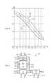
- FIG. 12shows particular measurements for an operation like that shown in FIG. 11C or 11 D.
- FIG. 12is a graph showing a measured current (Imeas) versus a gate-to-source voltage (Vgs).
- a measured current (Imeas)can be a current measured from a test output coupled to multiple test elements, like those shown in FIG. 5 .
- a threshold voltagecan be value established according to well understood techniques.
- a threshold voltagecan be a Vgs at which a drain-to-source current (IDS) has a predetermined value for a given drain-to-source voltage (VDS).
- IDSdrain-to-source current
- embodiments having memory sectionscan test transistors within memory cells, for some architectures (e.g., FIG. 8 ) it can be possible to test transistors within sense amplifiers of the memory section.
- FIG. 13One such embodiment is shown in FIG. 13 .
- the IC device 1300can include a column MUX/precharge section 1332 , a sense amplifier 1352 , and I/O section 1374 , and test section 1302 .
- a column MUX/precharge section 1332can be coupled between bit lines (BIT/BITN) and sense nodes 1350 -0/1. In response to a precharge signal (prebitn), column MUX/precharge section 1332 can precharge bit lines (BIT/BITN) to a precharge potential. In response to column select data (csel), column MUX/precharge section 1332 can couple a bit line pair (BIT/BITN) to sense nodes 1350 -0/1.
- a sense amplifier (SA) 1352can sense a data value on a selected bit line pair (BIT/BITN).
- sense nodes 1350 -0/1can be precharged to a SA precharge voltage by activation of SA precharge signal (presan).
- bit line precharge circuits in 1332can be disabled.
- a memory cellcan be coupled to a bit line pair (BIT/BITN), and the bit line pair coupled to sense nodes 1350 -0/1 by operation of column MUX/precharge section 1332 .
- a differential voltagecan develop across a bit line pair (BIT/BITN), and hence across sense nodes 1350 -0/1.
- SA 1352 of FIG. 13can also receive test signals (ntest/ptestn), which can disable portions of SA 1352 to enable transistors in other portions to be tested. Particular examples of such operations will be described in more detail below.
- An I/O section 1374can output data (dout) based on potentials across sense nodes 1350 -0/1, or can drive data on sense nodes 1350 -0/1 in response to input data (din).
- a data output (dout)will be driven based on a potential between sense nodes 1350 -0/1.
- sense nodes 1350 -0/1will be driven to different voltages according to an input data value (din).
- a test section 1302can include test elements as described herein, or equivalents. Such test elements can be enabled in response to a test enable signal (dbsel). When enabled, test voltages can be driven on outputs 1314 -0/1 and/or current flowing through outputs 1314 -0/1 can be measured. Further, signal paths for such test values can be very low leakage signals paths as described above.
- a column MUX/precharge section 1432that can be included in embodiments is shown in a block schematic diagram.
- the column MUX/precharge section 1332( FIG. 13 ) can be implemented using the column MUX/precharge section 1432 .
- precharge circuits1476 -0 to -3) can precharge their respective bit lines bit ⁇ n>/bitn ⁇ n> to a precharge voltage VDDpc.
- a column select circuit( 1476 -0 to -3) can couple its bit line pair to sense nodes 1450 -0/1.
- SA 1552a sense amplifier 1552 according to an embodiment is shown in schematic diagrams.
- SA 1552can be that shown as 1332 in FIG. 13 .
- SA 1552can include SA precharge circuits 1580 -0/1, p-channel sense transistors P 4 /P 5 and n-channel sense transistors N 7 /N 8 cross-coupled between sense nodes 1550 -0/1, a first enable transistor P 6 coupled between a first enable node 1582 -0 and a high power supply node VDD, a second enable transistor N 9 coupled between a second enable node 1582 -1 and a low power supply voltage VSS, a first test transistor N 10 coupled between first enable node 1582 -0 and a low power supply voltage VSS, and a second test transistor P 7 coupled between second enable node 1582 -1 and a high power supply voltage VDD.
- SA precharge circuits 1580 -0/1can be commonly controlled according to signal presan. When signal presan is active (low), SA precharge circuits 1580 -0/1 can precharge sense nodes 1550 -0/1 and enable nodes 1582 -0/1 to a SA precharge voltage (Vbias).
- Enable transistor P 6can be controlled according to signal saen to connect or isolate first enable node 1582 -0 from supply voltage VDD.
- enable transistor N 9can be controlled according to signal sae to connect or isolate second enable node 1582 -1 from supply voltage VSS.
- Test transistor N 10can be controlled according to signal ntest to disable sense transistors P 4 /P 5 and enable the testing of sense transistor N 7 or N 8 by coupling first enable node 1582 -0 to VSS.
- Test transistor P 7can be controlled according to signal ptestn to disable sense transistors N 7 /N 8 and enable the testing of sense transistor P 4 or P 5 by coupling second enable node 1582 -1 to VDD.
- FIGS. 13 to 15Cvarious sections of an IC device (i.e., FIGS. 13 to 15C ) that can enable a testing of sense amplifier transistors, various modes of operation for such a device will now be described with reference to FIG. 16 in conjunction with FIGS. 13 to 15C .
- FIG. 16is a table showing six different modes of operation for an IC device like that shown in FIGS. 13 to 15C .
- FIG. 16shows logic values for the various control signals of an IC device for each corresponding mode.
- the modesinclude: “Read” in which data can be read from the IC device; “Write” in which data can be written into the IC device; “DBTA” in which transistors within a memory array can be tested via bit lines; “DSTAN” in which n-channel transistors in a sense amplifier can be tested; “DSTAP” in which p-channel transistors in a sense amplifier can be tested; and “Offset” in which an offset voltage of a sense amplifier can be tested.
- dbsel0 disabling test elements within test section 1302
- wenable0 disabling write operations
- other control signalscan pulse. Such transitions are shown by values separated with a slash, and represent first transitions in an active read cycle operation.
- Sense amplifiersare normally off when unselected, but for the selected locations sae and saen transition to the “on” state (0/1 for sae and 1/0 for saen).
- Precharge signals presan and prebitnare normally “on” in the unselected locations (keeping the unselected bit lines and unselected sense amps precharged), but transition to “off” 0/1 when selected for the read operation.
- Turning off precharge circuitse.g., 1476 -0/1, 1580 -0/1) can enable a small signal to develop between bit lines (BL/BLN) without contention with the precharge circuits.
- Column select cselis normally off, but transitions to “on” 0/1 at the beginning of a read cycle (cseln is understood to be the complement of csel).
- the SA 1352can be activated by sae (0/1) and saen (I/O) to amplify the small signal, thereby driving sense nodes 1350 -0/1 to opposing voltages. Afterward, read enable signal can be activated (renable 0/1), and I/O section 1374 can drive read data on dout.
- signalscan pulse as shown in FIG. 16 .
- precharge signals presan and prebitnare normally “on” in the unselected locations (keeping the bit lines and SAs precharged), but transition to “off” 0/1 for the selected write location to allow the bit lines to be written to full complementary levels without contention with the precharge circuits.
- Column Select cselis normally off, but in a write mode can transition to “on” 0/1 at the beginning of the write cycle.
- a write enable signalcan be activated (wenable 0/1), and data at din can be driven on sense nodes 1350 -0/1 and bit lines of the written memory cell through a column MUX/precharge section 1332 .
- an IC device 1300in a DBTA mode, can operate in a DC mode, where timing clocks can be stopped and control signals can have either an “on” or “off” state.
- individual transistors within a memory arraycan be tested. Such testing, according to very particular embodiments, is shown in FIGS. 11A to 11D .
- an IC device 1300in a DSTAN mode, can also operate in a DC mode.
- n-channel devices within SA 1352can be tested.
- the column select circuits 1478 -0 to 3FIG. 14
- All of the column select circuitscan be deselected in this mode.
- FIG. 15Ashows a SA 1552 in a DSTAN mode.
- the particular embodiment of FIG. 15Ashows a testing of transistor N 7 .
- sense node 1550 -0can be driven (via a test element) to a voltage less than a threshold voltage of the other n-channel transistor (i.e., Vtn of N 8 ). In one very particular embodiment, such a level can be about 200 mV.
- the other sense node 1550 -1can be swept from 0 to VDD (or at least to a level significantly higher than the Vtn of N 8 ) via another test element.
- a current (Imeas) flowing at sense node 1550 -0can be monitored to give current-to-voltage (IN) characteristics (and thus the Vtn) of N 7 in a linear mode of operation.
- voltages applied to sense nodes 1550 -0/1can be reversed.
- an IC device 1300in a DSTAP mode, can also operate in a DC mode.
- Signals csel, prebitn, renable, wenable, and dbselcan have the same values as the DSTAN mode.
- FIG. 15Bshows a SA 1552 in a DSTAP mode.
- the particular embodiment of FIG. 15Bshows a testing of transistor P 4 .
- sense node 1550 -0can be driven (via a test element) to a voltage less than a threshold voltage of the other p-channel transistor (i.e., Vtp of P 5 ). In one very particular embodiment, such a level can be about VDD-200 mV.
- the other sense node 1550 -1can be swept from VDD to 0 (or at least to a level significantly lower than Vtp of P 5 ) via another test element.
- a current (Imeas) flowing at sense node 1550 -0can be monitored to give current-to-voltage (IN) characteristics (and thus the Vtp) of P 4 in a linear mode of operation.
- voltages applied to sense nodes 1550 -0/1can be reversed.
- an IC device 1300in an Offset mode, can operate in an AC mode of operation, with system clocks running. However, unlike a Read or Write mode, SA 1352 can be controlled through test section 1302 . In an Offset mode, an offset of cross-coupled n- and p-channel transistors (i.e., P 4 /P 5 , N 7 /N 8 ) inside SA 1352 can be tested.
- P 4 /P 5 , N 7 /N 8cross-coupled n- and p-channel transistors
- prebitn1, disabling bit line precharge circuits 1476 -0/1.
- wenable0, disabling write amplifiers within I/O section 1374 .
- renable1, enabling I/O section 1374 to drive dout based on voltages between sense nodes 1350 -0/1.
- FIG. 15Cshows SA 1552 in an Offset mode that can be used to measure the as-fabricated sense amplifier offset.
- Enable transistors P 6 and N 9can be activated by pulsing saen (I/O) and sae (0/1), as in a read operation.
- test elements within test section 1302can apply a sequence of differential voltages to sense nodes 1350 -0/1.
- An Offset testcan begin with a reasonably large differential across sense nodes 1350 -0/1 (i.e., a differential know to be greater than any offset voltage of the SA 1352 ).
- the differential voltage at which the output value switchescan be determined to be the offset voltage of the SA 1352 .
- the offset voltage of the SA 1352is determined by performing a binary search of the differential voltages to sense nodes 1350 -0/1.
- FIG. 17shows an alternate configuration for a sense amplifier 1552 ′ like that shown in FIGS. 15A to 15C .
- signals saen and ntestcan be the same.
- sae and ptestncan be the same.
- signal routingcan be advantageously compact.
- FIGS. 15A to 15Cshows test modes of operation for one particular sense amplifier circuit, it is understood that other embodiments can include any other suitable sense amplifier circuits. Two of many possible alternate embodiments for testing different sense amplifier circuits will now be described.
- FIG. 18shows an IC device 1800 having a “regenerative” type SA 1852 .
- IC device 1800can include column select circuits 1832 -0/1 which can couple bit lines (BL/BLNs) to sense nodes 1850 -0/1 as described for embodiments herein, or equivalents.
- Sense nodes 1850 -0/1can be coupled to test outputs (not shown) via test elements (not shown).
- SA 1852can include cross-coupled p-channel and n-channel transistors (P 4 /P 5 , N 7 /N 8 ) and an enable transistor N 9 , as described for other embodiments.
- SA 1852can include precharge transistors P 8 /P 9 .
- FIG. 19shows an IC device 1900 having an analog comparator type SA 1952 .
- IC device 1900can include sections like those of FIG. 18 .
- SA 1952can include differential input transistors N 11 /N 12 having gates coupled to sense nodes 1950 -0/1, and source-drain paths coupled between transistors N 7 /N 8 and enable transistor N 9 .
- An Offset test for IC device 1900can occur in a like fashion to that of FIG. 18 .
- Integrated circuit devicesmay provide improved characterization of device elements by providing high fidelity test paths to various internal nodes of the device.
- transistors within individual memory cellscan be characterized.
- transistors within sense amplifiers and/or a sense amplifier offset voltagecan be accurately characterized. Such data can enable circuits and threshold levels to be optimized to actual transistor response, as opposed to being constructed with “guard-band” responses designed to accommodate a wide range of variation in transistor and/or SA response.
- test elements 102can be used for measurement and characterization of analog circuits, such as a comparator in a flash analog to digital converter.
- analog circuitssuch as a comparator in a flash analog to digital converter.
- test operation described abovecan also be used to determine as-fabricated offsets in such analog circuits.
Landscapes
- Physics & Mathematics (AREA)
- General Physics & Mathematics (AREA)
- Engineering & Computer Science (AREA)
- Microelectronics & Electronic Packaging (AREA)
- Tests Of Electronic Circuits (AREA)
- For Increasing The Reliability Of Semiconductor Memories (AREA)
Abstract
Description
The present invention relates generally to integrated circuit devices, and more particularly to test circuits for integrated circuit devices for characterizing transistors therein.
Integrated circuit devices can include circuit sections, such as memory circuits, that can be designed for high performance operations. Memory circuits, such as static random access memory (SRAMs) typically have a number of memory cells arranged into one or more arrays composed of multiple transistors. The performance characteristics and yield of the circuit sections in the integrated circuit can be affected by variations in the electrical characteristics of the transistors, such as threshold voltages, current drive, etc., and circuit characteristics, such as offset voltages.
While it is desirable to test transistor characteristics and circuit characteristics within memory cells and other circuit sections of the integrated circuit, data input/output (I/O) paths can introduce leakage currents that can make it very difficult to achieve high fidelity measurements.
Various embodiments will now be described in detail with reference to a number of drawings. The embodiments show integrated circuit device test circuits and methods that can reduce leakage currents in a data input/output (I/O) path and thereby enable accurate testing (including characterization) of circuit elements within the device.
In the various embodiments below, like items are referred to by the same reference character but the leading digits corresponding to the figure number.
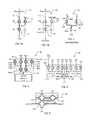
Referring now toFIGS. 1A and 1B , an integrated circuit (IC)device 100 according to an embodiment is shown in a block schematic diagram. AnIC device 100 can include one ormore test elements 102. Atest element 102 can provide a data path to enable signals to travel to a section of the device (in the embodiment shown a memory section). In addition, atest element 102 can enable low current leakage test paths to enable testing (including characterization) of elements within the section. Atest element 102 can include afirst switch 104, asecond switch 106, and atest switch 110. Afirst switch 104 can be coupled between asection node 112 and anintermediate node 108. Asecond switch 106 can be coupled betweenintermediate node 108 and anoutput node 114. Atest switch 110 can be coupled betweenintermediate node 108 and a forcedvoltage node 116. One ormore test elements 102 can be used to couple input and output data signals, e.g., test signals, to a circuit under test within the integratedcircuit 100. For example, thetest element 102 can be used to enable testing and characterization of component transistors or sub-circuits of analog circuit sections in an integrated circuit device, such as a flash analog to digital converter, as well as logic and memory sections.
In some embodiments, asection node 112 can be a node within a memory section of an integrated circuit device. For example, asection node 112 can include any of: a bit line or transistor gate, source, or drain within a selected memory cell. In addition or alternatively, asection node 112 can include nodes within circuits positioned between a memory cell array and input/outputs (I/Os) of a memory section. For example, amemory section node 112 can include any of: a sense amplifier circuit sense node, a transistor within a sense amplifier circuit, or switching circuits in an I/O path (e.g. column multiplexer, column select signals, etc.). It is noted that there can be intervening circuits between asection node 112 and atest element 102. It is also noted that whilenode 114 is referred to as an “output” node, it can serve to input data to a memory section in some embodiments.
Atest element 102 can have two modes of operation, a standard mode and a low leakage cutoff mode.FIG. 1A shows atest element 102 in a standard mode. In a standard mode, first and second switches (104,106) can be configured to provide a low impedance path, whiletest switch 110 can be configured to provide a high impedance path. Consequently, a signal path can be enabled betweenmemory section node 112 andoutput node 114. At the same time, forcedvoltage node 116 can be isolated fromintermediate node 108.
The arrangement ofFIG. 1B is in contrast to a conventional MUX shown inFIG. 2 . Aconventional MUX 103 can includeswitches common output node 109 anddifferent input nodes switch 107, even if theother switch 105 is in an off state (i.e., configured to provide a high impedance path), becauseinput node 111 is de-asserted (i.e., at a voltage VSS that is different than a voltage Vtest at output node109), leakage current (Ileak) can flow throughswitch 105, contributing to error in a measured current Imeas. This leakage current can have a significant effect on the fidelity of measurements when many switches are connected to the same node, as the leakage current flowing through each switch in the off state contributes to the error in the measured current Imeas.
Referring back toFIGS. 1A and 1B , anoutput node 114 can be a node internal to anIC device 100. For example, anoutput node 114 can be a conductive connection betweentest element 102 and testing circuits formed on a same IC, such as built-in self-test (BIST) circuits. In addition or alternatively, anoutput node 114 can be an external connection to anIC device 100. For example, anoutput node 114 can include a physical connection to IC device100 (e.g., pads, leads, pins, landing, balls, circuit board traces, etc.). In such cases, an external test device (wafer probe, automatic test equipment, etc.) can apply test conditions to testelement 102. It is noted that there may be intervening circuits between atest element 102 and anoutput node 114.
In contrast, test element302-0 is in the low leakage cutoff mode. A voltage Vsig, which can be the same as, or substantially the same as Vtest, can be applied to intermediate node308-0 through test switch310-0. Consequently, there can be little or no leakage current (Ileak=0) flowing tooutput node 314 from test element302-0 to interfere with current Imeas.
While FIGS.1A/B and3 have shown test elements with one first switch and one test switch, alternate embodiments can include multiple first switches per one test switch. One such embodiment is shown inFIG. 4 .
InFIG. 4 , test element402-1 is in a standard mode. In the standard mode, test switch410-1 can be non-conductive. At the same time, one of the first switches, e.g., switch404-11, can be conductive, while the remaining first switches (404-10 and -404-12 to -1n) can be non-conductive. Second switch406-1 can also be conductive.
Test elements according to embodiments shown herein can be formed with any circuit elements suitable for achieving desired reductions in leakage current at an output node. Some embodiments can form test elements with transistors appropriate to the manufacturing process. In particular embodiments, test elements can be formed with insulated gate field effect transistors (e.g., MOS transistors).
InFIG. 5 ,first switch 504,second switch 506 andtest switch 510 can be formed from complementary MOS (CMOS) passgates, each including complementary conductivity (i.e., n-channel and p-channel) transistors arranged in parallel with one another. Gates of the transistors can be driven with complementary control signals SELECT/SELECTN. Accordingly, when signals SELECT/SELECTN are high/low, respectively,test element 502 can be in a standard mode, first and second switches (504/506) can be conductive, andtest switch 510 can be non-conductive. When signals SELECT/SELECTN are low/high, respectively,test element 502 can be in a low leakage cutoff mode, with first and second switches (504/506) being non-conductive, andtest switch 510 being conductive. Therefore, in the low leakage cutoff mode, when the voltage atforced voltage node 516 is driven to substantially the same voltage as theoutput node 514, thetest switch 510 can enable driving of theintermediate node 508 with substantially the same voltage as theoutput node 514.
In one embodiment, signals SELECT/SELECTN can be boosted voltage signals in a test mode. For example, in a non-boosted mode, SELECT can be driven to a high power supply voltage (VDD) and SELECTN can be driven to a low power supply voltage (e.g., VSS). However, in a test mode of operation, signal SELECT can be driven to boosted voltage (e.g., VPP>VDD). In addition or alternatively, signal SELECTN can be driven to a boosted voltage (e.g., VBB<VSS). Such boosted signal levels can enable lower impedance when switches are conductive, and less leakage when switches are non-conductive, as compared to the non-boosted mode of operation.
It is understood that whileFIG. 5 shows a test element having switches (504,506,510) controlled by a common signal pair, alternate embodiments can control such elements separately.
It is also noted that in an alternate embodiment, any ofswitches
In designing IC devices, is desirable to utilize as little substrate area as possible to increase economies of scale and/or reduce signal routing lengths. Compact area implementations of test elements will now be described.
Referring now toFIG. 7 , anintegrated circuit device 700 according to another embodiment is shown in block schematic diagram. AnIC device 700 can include a first MUX layer730-0, a second MUX layer730-1, and amemory section 746. Atest circuit 718 is also shown that may, or may not, be part ofIC device 700.
A first MUX layer730-0 can include multiple test elements702-0 to -m, each of which can take the form of any of the test elements shown herein, or equivalents. Each of test elements702-0/1 can be coupled to an output node714-0/1, which is coupled to, or which can be coupled to,test circuit 718.
A second MUX layer730-1 can include a number of column MUXes732-00 to732-1n. Column MUXes can selectively couple bit lines (two shown as734-0/1) of amemory section 746 to first MUX layer730-0. In some embodiments, column MUXes (732-00 to -1n) can include test elements as described herein, or equivalents. However, in other embodiments, column MUXes (732-00 to -1n) can include conventional MUX circuits.
It is understood that first and second MUX layers (730-0 and730-1) can enable signal paths in response to column select data, which can be generated from a memory address, or the like.
In the embodiment shown, amemory section 746 can include bit line pairs (one shown as734-0/1) coupled to a number of memory cells (one shown as736).Memory cells 736 can be coupled to a corresponding bit line pair734-0/1 by operation of aword line 738 driven by aword line driver 740. In the particular embodiment shown, amemory cell 736 can be a six-transistor (6T) static random access memory (SRAM) cell, having two p-channel transistors P0/P1 cross-coupled between storage nodes748-0/1, two n-channel transistors N2/N3 cross-coupled between storage nodes748-0/1, and two access transistors N0/N1 that can couple storage nodes748-0/1 to bit lines734-0/1. Memory cells (e.g.,736) can be coupled between a high array powersupply voltage node 744 and a low array powersupply voltage node 742.
Aword line driver 740 can drive aword line 738 between a high voltage VDDWL and a low voltage VSSWL. A voltage VDDWL can be substantially higher than a high array supply voltage VDDAR, and VSSWL can be substantially lower than VSSAR. A boosted low voltage VSSWL can force access transistors N0/N1 to very low leakage states. A boosted high voltage VDDWL can eliminate any voltage threshold drop across access transistors N0/N1, and place such transistors into very low impedance states to improve current/voltage readings in test operations.
Atest circuit 718 can include a switch network718-0, voltage sources718-1, a current measuring circuit718-2, and a sequencer718-3. A switch network718-0 can couple test output nodes714-0/1 to various sections withintest circuit 718. Voltage sources718-1 can provide various test voltages for application to output nodes714-0/1. Such test voltages can be constant voltages, variable voltages (e.g., a sweep over a range), or differential voltages for application between a pair of output nodes714-0/1. A current measuring circuit718-2 can measure a current flowing through an output node714-0/1. A sequencer718-3 can execute a test sequence by applying test voltages, and optionally control signals to thedevice 700. The sequencer718-3 can also execute test sequences that include generating addresses for thememory section 746 that enable accesses to a selected cell in thememory section 746, and thereby enable the execution of test sequences and the application of test voltages to the selected cell.
In a standard mode of operation, all test elements702-0 to -m can be placed in a standard mode of operation, enabling read and/or write paths tomemory cells 736 via bit lines.
In a test mode of operation, two of test elements702-0 to -m can be placed in a standard mode of operation, while remaining test elements can be placed in the low leakage cutoff mode. The two test elements in the standard mode can enabletest circuit 718 to apply test conditions tomemory section 746. Test conditions according to particular embodiments will be described in more detail below.
Referring now toFIG. 8 , anintegrated circuit device 800 according to another embodiment is shown in block schematic diagram. AnIC device 800 can include sections likeFIG. 7 .FIG. 8 differs fromFIG. 7 in that a columnselect layer 848 and asense amplifier 852 can be included between bit lines834-0/1 and second MUX layer830-1.
A columnselect layer 848 can include column select circuits860-0 to -k that couple bit lines (e.g.,834-0/1) to MUX layers (830-0/1) based on column select values.
While embodiments can include various types of sense amplifiers, in the particular embodiment ofFIG. 8 ,sense amplifier 852 can include two p-channel sense transistors P2/P3 cross coupled between sense node850-0/1, two n-channel sense transistors N4/N5 cross-coupled between sense nodes848-0/1, and an enable transistor N6.Sense amplifier 852 can be coupled between a high sense amplifier supply voltage VDDSA and a low sense amplifier supply voltage VSSSA.
In an arrangement like that ofFIG. 8 , asense amplifier 852 can also be tested through test elements802-00 to -1n. When testing asense amplifier 852, a columnselect layer 848 can be driven to a high impedance state to isolate asense amplifier 852 from bit lines834-0/1. Sense amplifier test conditions according to particular embodiments will be described in more detail below.
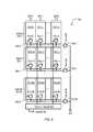
Embodiments of the invention can include memory sections having memory cells organized into banks. One such embodiment is shown inFIG. 9 . Referring toFIG. 9 , anintegrated circuit device 900 can include a number of banks962-0 to -M. Each bank (962-0 to -M) can include columns966-0 to -N. Each column (966-0 to -N) within a bank can be coupled to a bank I/O node966-0 to -M by column MUXes932-00 to -Mx. Bank I/O nodes (966-0 to -M) can be coupled tooutput node 914 by bank selectors902-0 to -M. Any of column MUXes (932-00 to -Mx) and/or bank selectors (902-0 to -M) can include test elements as described herein, or equivalents
Atest column decoder 968 can enable and disable test elements within column MUXes (932-00 to -Mx) and/or bank selectors (902-0 to -M) to enable test modes of operation.
Accordingly, circuit elements within any of the banks can be tested as described herein, or equivalents.
Atest circuit 1018 can apply test conditions to amemory array 1070 and derive test results frommemory array 1070 throughtest elements 1002. In the embodiment shown, atest circuit 1018 can also controlword line driver 1040 andsubstrate control circuit 1072. As noted above, atest circuit 1018 may, or may not, be part ofIC device 1000.
Having described IC devices with test elements that can enable accurate testing of circuit devices, particular test operations according to embodiments will now be described.
In the test operation, aword line 1138 can be driven to a level that enables pass transistors N0/N1. Such a word line voltage can be substantially higher than an array high supply voltage VDDAR. In the particular embodiment shown, aword line 1138 can be driven to 1.2V while VDDAR=0.6V.
A first test voltage can be applied to a gate of TUT P0 through test element1102-0 and access transistor N0. Thus, test element1102-0 can be in a standard state, allowing a signal path to output node1114-0. In contrast, any test elements (i.e.,1102-1) coupled to the same output node1114-0 can be in a low leakage cutoff mode, thus an intermediate node within such test elements can be driven to a voltage that can match that at output node1114-0. In the particular embodiment shown, bit line1134-0 can be driven to 0V, thus non-selected test element1102-1 can apply 0V to its intermediate node.
A second “sweeping” test voltage can be applied to a drain of TUT P0 through test element1102-2 and access device N1. Thus, test element1102-2 can be in a standard mode while test element (i.e.,1102-3) coupled to the same output node1114-1 can be in a low leakage cutoff mode. A sweeping voltage can vary over time, enabling multiple current (Imeas) values to be acquired. Non-selected test element1102-3 can apply substantially the same sweeping voltage to its internal node. In the particular embodiment shown, bit line1134-1 can be swept between 0V and 0.5V, and a resulting current (Imeas) can be measured at various points, thus providing an accurate characterization of TUT P0.
It is understood that the other p-channel load transistor P1 can be tested in the same fashion as P0 by swapping the test voltages applied to the bit lines.
In the test operation, aword line 1138 can be driven as inFIG. 11A . However, in the embodiment shown an array high supply voltage VDDAR can be 0.8V.
A first sweeping voltage can be applied to a gate of TUT P0 through test element1102-0 and access transistor N0. In addition, a low array power supply voltage VSSAR can be swept in the same fashion. Selected test element1102-0 can be in a standard state, while non-selected test elements (e.g.,1102-1) coupled to a same output node1114-0 can be in a low leakage cutoff mode, and receive the same, or substantially same sweeping voltage. In the embodiment shown, a sweeping voltage can be between 0.6 and 0 V.
A second test voltage can be applied to a drain of TUT P0 through test element1102-2 and access device N1. Selected test element1102-2 can be in a standard mode and non-selected test elements (i.e.,1102-3) can be in a low leakage cutoff mode and receive substantially the same voltage. In the particular embodiment shown, bit line1134-1 can receive 0.6V.
Current (Imeas) through bit line1134-1 can be measured to provide accurate characterization of TUT P0.
It is understood that the other p-channel load transistor P1 can be tested in the same fashion as P0 by swapping the test voltages applied to the bit lines.
In the test operation, aword line 1138 can be driven to a test level which gives a desired current response based on the drain-source voltage (VDS) applied to TUT N0. In the particular embodiment shown, aword line 1138 can be driven to 0.6V. An array high supply voltage VDDAR can be 1.2V.
A first sweeping voltage can be applied to a drain of transistor N0 by way of bit line1134-0. A selected test element1102-0 can be in a standard state, while non-selected test elements (e.g.,1102-1) can be coupled to receive the same, or substantially the same, sweeping voltage. In the embodiment shown, a sweeping voltage can be between 0.6 and 0 V.
A second test voltage can be applied to a gate of transistor N3 to ensure N3 provides a current path to VSSAR for TUT N0. Selected test element1102-2 can be in a standard mode and non-selected test elements (i.e.,1102-3) can be in a low leakage cutoff mode. In the particular embodiment shown, bit line1134-1 and non-selected test element1102-3 can receive 1.2V.
Current (Imeas) through bit line1134-0 can be measured to provide accurate characterization of TUT N0.
It is understood that the other access transistor N1 can be tested in the same fashion as N0 by swapping the test voltages applied to the bit lines.
In the test operation, aword line 1138 can be driven to a test level that enables access transistors N0/N1. In the particular embodiment shown, aword line 1138 can be driven to 1.2V. An array high supply voltage VDDAR can be 0.6V. A substrate voltage for transistors P0/1 (VPsub) can be driven to 1.6V.
A first test voltage can be applied to a gate of transistor N2 through access transistor N0. Selected test element1102-0 can be in a standard mode, while non-selected test elements (e.g.,1102-1) can be in the low leakage cutoff mode.
A second sweeping test voltage can be applied to a drain of transistor N2 through access transistor N1 to generate a current Imeas that varies according to the VDS of TUT N2. In the particular embodiment shown, such sweeping voltage can be between 0.2 and 0.6 V.
It is noted that body biases (VNsub) can be applied to the TUT (e.g., N2/N3) to raise threshold voltages of such devices. This can reduce unwanted currents in thememory cell 1136. In the particular embodiment shown, such biases can be between 0 and 0.4 V.
It is understood that the other n-channel pull-down transistor N3 can be tested in the same fashion as N2 by swapping the test voltages applied to the bit lines.
It is noted that in the testing operations shown inFIGS. 11A to 11D , it may be desirable to first place thememory cell 1136 into a desired state (e.g., set storage nodes1148-0/1 to desired complementary states) with a write operation prior to the test operation.
Test operations such as those described herein can result in high fidelity characterization of transistors within a tested portion of an IC device. In some embodiments, current accuracy can be within 1% using appropriate biasing conditions.FIG. 12 shows particular measurements for an operation like that shown inFIG. 11C or11D.
It is noted that a threshold voltage (Vt) can be value established according to well understood techniques. For example, a threshold voltage can be a Vgs at which a drain-to-source current (IDS) has a predetermined value for a given drain-to-source voltage (VDS).
As noted above, while embodiments having memory sections can test transistors within memory cells, for some architectures (e.g.,FIG. 8 ) it can be possible to test transistors within sense amplifiers of the memory section. One such embodiment is shown inFIG. 13 .
Referring now toFIG. 13 , anIC device 1300 according to another embodiment is shown in a block schematic diagram. TheIC device 1300 can include a column MUX/precharge section 1332, asense amplifier 1352, and I/O section 1374, andtest section 1302.
A column MUX/precharge section 1332 can be coupled between bit lines (BIT/BITN) and sense nodes1350-0/1. In response to a precharge signal (prebitn), column MUX/precharge section 1332 can precharge bit lines (BIT/BITN) to a precharge potential. In response to column select data (csel), column MUX/precharge section 1332 can couple a bit line pair (BIT/BITN) to sense nodes1350-0/1.
A sense amplifier (SA)1352 can sense a data value on a selected bit line pair (BIT/BITN). In a sense operation, prior to sensing a data value, sense nodes1350-0/1 can be precharged to a SA precharge voltage by activation of SA precharge signal (presan). When sensing a data value, bit line precharge circuits in1332 can be disabled. A memory cell can be coupled to a bit line pair (BIT/BITN), and the bit line pair coupled to sense nodes1350-0/1 by operation of column MUX/precharge section 1332. According to a data value stored in the memory cell, a differential voltage can develop across a bit line pair (BIT/BITN), and hence across sense nodes1350-0/1. When sense amplifier enable signals (sae/saen) are activated, the sense nodes1350-0/1 can be driven to opposing voltages based on the differential voltage.
Unlike a conventional sense amplifier,SA 1352 ofFIG. 13 can also receive test signals (ntest/ptestn), which can disable portions ofSA 1352 to enable transistors in other portions to be tested. Particular examples of such operations will be described in more detail below.
An I/O section 1374 can output data (dout) based on potentials across sense nodes1350-0/1, or can drive data on sense nodes1350-0/1 in response to input data (din). In particular, in response to an active read enable signal (renable), a data output (dout) will be driven based on a potential between sense nodes1350-0/1. In response to an active write enable signal (wenable), sense nodes1350-0/1 will be driven to different voltages according to an input data value (din).
Atest section 1302 can include test elements as described herein, or equivalents. Such test elements can be enabled in response to a test enable signal (dbsel). When enabled, test voltages can be driven on outputs1314-0/1 and/or current flowing through outputs1314-0/1 can be measured. Further, signal paths for such test values can be very low leakage signals paths as described above.
Referring toFIG. 14 , a column MUX/precharge section 1432 that can be included in embodiments is shown in a block schematic diagram. In one embodiment, the column MUX/precharge section1332 (FIG. 13 ) can be implemented using the column MUX/precharge section 1432.
A column MUX/precharge section 1432 can include bit line precharge circuits1476-0 to -3 and column select circuits1478-0 to -3, each of which can be coupled to a corresponding bit line pair bit<n>, bitn<n> (where n=0 to 3). In response to an active precharge signal prebitn, precharge circuits (1476-0 to -3) can precharge their respective bit lines bit<n>/bitn<n> to a precharge voltage VDDpc. In response to particular column select signals csel<n>, cseln<n> (where n=0 to 3), a column select circuit (1476-0 to -3) can couple its bit line pair to sense nodes1450-0/1.
Referring toFIG. 15A to 15C , a sense amplifier (SA)1552 according to an embodiment is shown in schematic diagrams. In one embodiment,SA 1552 can be that shown as1332 inFIG. 13 .
SA precharge circuits1580-0/1 can be commonly controlled according to signal presan. When signal presan is active (low), SA precharge circuits1580-0/1 can precharge sense nodes1550-0/1 and enable nodes1582-0/1 to a SA precharge voltage (Vbias). Enable transistor P6 can be controlled according to signal saen to connect or isolate first enable node1582-0 from supply voltage VDD. Similarly, enable transistor N9 can be controlled according to signal sae to connect or isolate second enable node1582-1 from supply voltage VSS. Test transistor N10 can be controlled according to signal ntest to disable sense transistors P4/P5 and enable the testing of sense transistor N7 or N8 by coupling first enable node1582-0 to VSS. Test transistor P7 can be controlled according to signal ptestn to disable sense transistors N7/N8 and enable the testing of sense transistor P4 or P5 by coupling second enable node1582-1 to VDD.
Having described various sections of an IC device (i.e.,FIGS. 13 to 15C ) that can enable a testing of sense amplifier transistors, various modes of operation for such a device will now be described with reference toFIG. 16 in conjunction withFIGS. 13 to 15C .
Referring now toFIG. 16 in conjunction withFIGS. 13 ,14 and15A, in a Read mode, dbsel=0 disabling test elements withintest section 1302, wenable=0 disabling write operations, and ntest=0/ptestn=1 disabling test devices withinSA 1352/1552. When a selected memory cell is accessed, other control signals can pulse. Such transitions are shown by values separated with a slash, and represent first transitions in an active read cycle operation. Sense amplifiers are normally off when unselected, but for the selected locations sae and saen transition to the “on” state (0/1 for sae and 1/0 for saen). Precharge signals presan and prebitn are normally “on” in the unselected locations (keeping the unselected bit lines and unselected sense amps precharged), but transition to “off” 0/1 when selected for the read operation. Turning off precharge circuits (e.g.,1476-0/1,1580-0/1) can enable a small signal to develop between bit lines (BL/BLN) without contention with the precharge circuits. Column select csel is normally off, but transitions to “on” 0/1 at the beginning of a read cycle (cseln is understood to be the complement of csel). TheSA 1352 can be activated by sae (0/1) and saen (I/O) to amplify the small signal, thereby driving sense nodes1350-0/1 to opposing voltages. Afterward, read enable signal can be activated (renable 0/1), and I/O section 1374 can drive read data on dout.
Referring again toFIG. 16 in conjunction withFIGS. 13 ,14 and15A, in a Write mode, dbsel=0, and ntest=0/ptestn=1 as in the Read mode. Further, renable=0, disabling read amplifiers in I/O section 1374. When a selected memory cell is written, signals can pulse as shown inFIG. 16 . In particular, precharge signals presan and prebitn are normally “on” in the unselected locations (keeping the bit lines and SAs precharged), but transition to “off” 0/1 for the selected write location to allow the bit lines to be written to full complementary levels without contention with the precharge circuits.SA 1352 can be disabled with sae=0, saen=1. Column Select csel is normally off, but in a write mode can transition to “on” 0/1 at the beginning of the write cycle. A write enable signal can be activated (wenable 0/1), and data at din can be driven on sense nodes1350-0/1 and bit lines of the written memory cell through a column MUX/precharge section 1332.
Referring again toFIG. 16 in conjunction withFIGS. 13 ,14 and15A, in a DBTA mode, anIC device 1300 can operate in a DC mode, where timing clocks can be stopped and control signals can have either an “on” or “off” state. In a DBTA mode, individual transistors within a memory array can be tested. Such testing, according to very particular embodiments, is shown inFIGS. 11A to 11D . Column select signal csel can have an enable state (csel=1), coupling bit lines (BL/BLN) to sense nodes1350-0/1.SA 1352 can be disabled (sae=0 and saen=1). In addition, in order to more fully removeSA 1352 from a test path, test signals can be driven to active levels (ntest=1 and ptestn=0), thereby disabling cross-coupled transistors withinSA 1352. Precharge circuits for both bit lines1476-0/1 and the SA nodes1550-01/can also disabled, to not interfere with the testing. Signal dbsel can be active (dbsel=1), enabling test elements withintest section 1302 to provide high fidelity (i.e., low leakage current) test signal paths to transistors within a memory cell being tested. Signals renable and wenable can both be disabled.
Referring once again toFIG. 16 in conjunction withFIGS. 13 ,14 and15A, in a DSTAN mode, anIC device 1300 can also operate in a DC mode. In a DSTAN mode, n-channel devices withinSA 1352 can be tested. Signal csel is inactive (csel=0), isolating bit lines BL/BLN from anSA 1352, and bit line precharge circuits1476-0/1 can be disabled (prebitn=1). If more than one bit line BL/BLN is coupled to theSA 1352 by parallel multiplexers, such as the column select circuits1478-0 to 3 (FIG. 14 ), then all of the column select circuits can be deselected in this mode. Write amplifiers and read amplifiers in I/O section 1374 can be disabled (renable=0, wenable=0). Test elements withintest section 1302 can be enabled (dbsel=1) to provide high fidelity test paths toSA 1352.
Referring now toFIG. 16 in conjunction withFIGS. 13 ,14 and15B, in a DSTAP mode, anIC device 1300 can also operate in a DC mode. Signals csel, prebitn, renable, wenable, and dbsel can have the same values as the DSTAN mode.
Referring now toFIG. 16 in conjunction withFIGS. 13 ,14 and15C, in an Offset mode, anIC device 1300 can operate in an AC mode of operation, with system clocks running. However, unlike a Read or Write mode,SA 1352 can be controlled throughtest section 1302. In an Offset mode, an offset of cross-coupled n- and p-channel transistors (i.e., P4/P5, N7/N8) insideSA 1352 can be tested.
Signal csel can be disabled (csel=0), isolating bit lines BL/BLN from sense nodes1350-0/1. In the embodiment shown, prebitn=1, disabling bit line precharge circuits1476-0/1. Signal dbsel can be active (dbsel=1) enabling test elements withintest section 1302. In addition, wenable=0, disabling write amplifiers within I/O section 1374. However, renable=1, enabling I/O section 1374 to drive dout based on voltages between sense nodes1350-0/1.
WhileFIGS. 15A to 15C shows test modes of operation for one particular sense amplifier circuit, it is understood that other embodiments can include any other suitable sense amplifier circuits. Two of many possible alternate embodiments for testing different sense amplifier circuits will now be described.
An Offset test forIC device 1800 can start with precharge devices P8/P9 being disabled (prch=1). A reasonably large differential voltage can be generated across sense nodes1850-0/1.SA 1852 can be activated (saen=0/1 pulse) to generate an output value. Such actions can be repeated with reduced differential values, as described forFIG. 15C until an output value changes. In alternative embodiments, a linear search or a binary search of the differential voltage can be performed to determine the offset voltage.
An Offset test forIC device 1900 can occur in a like fashion to that ofFIG. 18 . Precharge devices P8/P9 can be disabled (prch=1), and a reasonably large differential voltage can be generated across sense nodes1950-0/1.SA 1952 can be activated (saen=0/1 pulse) to generate an output value (SAO/SAON). Such actions can be repeated with reduced differential values, as described forFIG. 15C until an output value changes.
Integrated circuit devices according to embodiments shown herein, and equivalents, may provide improved characterization of device elements by providing high fidelity test paths to various internal nodes of the device.
In very particular SRAM embodiments, transistors within individual memory cells can be characterized. In addition or alternatively, transistors within sense amplifiers and/or a sense amplifier offset voltage can be accurately characterized. Such data can enable circuits and threshold levels to be optimized to actual transistor response, as opposed to being constructed with “guard-band” responses designed to accommodate a wide range of variation in transistor and/or SA response.
In alternative embodiments, thetest elements 102 can be used for measurement and characterization of analog circuits, such as a comparator in a flash analog to digital converter. Thus, the various embodiments and test operation described above can also be used to determine as-fabricated offsets in such analog circuits.
It should be appreciated that in the foregoing description of exemplary embodiments of the invention, various features of the invention are sometimes grouped together in a single embodiment, figure, or description thereof for the purpose of streamlining the disclosure aiding in the understanding of one or more of the various inventive aspects. This method of disclosure, however, is not to be interpreted as reflecting an intention that the claimed invention requires more features than are expressly recited in each claim. Rather, as the following claims reflect, inventive aspects lie in less than all features of a single foregoing disclosed embodiment. Thus, the claims following the detailed description are hereby expressly incorporated into this detailed description, with each claim standing on its own as a separate embodiment of this invention.
It is also understood that the embodiments of the invention may be practiced in the absence of an element and/or step not specifically disclosed. That is, an inventive feature of the invention may be elimination of an element.
Accordingly, while the various aspects of the particular embodiments set forth herein have been described in detail, the present invention could be subject to various changes, substitutions, and alterations without departing from the spirit and scope of the invention.
Claims (31)
1. An integrated circuit device, comprising:
a plurality of test elements, each comprising
at least one first switch coupled between a node within a tested section and an intermediate node,
a test switch coupled between the intermediate node and a forced voltage node, and
a second switch coupled between the intermediate node and an output node; wherein
the forced voltage node is selectively coupled to receive a forced voltage substantially the same as a test voltage applied to the output node.
2. The integrated circuit device ofclaim 1 , wherein:
each test element of the plurality of test elements is operable in a first mode, the at least one first switch being coupled to provide a low impedance path and the test switch being coupled to provide a high impedance path in the first mode; and
each test element of the plurality of test elements is operable in a second mode, the at least one first switch being coupled to provide a high impedance path and the test switch being coupled to provide a low impedance path in the second mode.
3. The integrated circuit device ofclaim 1 , wherein:
the at least one first switch, test switch, and second switch each comprise transistors of different conductivity types having current paths arranged in parallel with one another.
4. The integrated circuit device ofclaim 1 , wherein:
the at least one first switch, test switch, and second switch each comprise at least one transistor; and
each test element fits within no more than three transistor pitches.
5. The integrated circuit device ofclaim 1 , wherein:
the at least one first switch includes a plurality of first parallel switches, each first parallel switch being coupled between a node of the integrated circuit and the intermediate node;
each test element of the plurality of test elements is operable in a first mode, the test switch being coupled to provide a high impedance path in the first mode, at least one parallel switch of the plurality of first parallel switches being coupled to provide a low impedance path in the first mode, and the first parallel switches other than the at least one parallel switch being coupled to provide a high impedance path in the first mode; and
each test element of the plurality of test elements is operable in a second mode, the test switch being coupled to provide a low impedance path and all of the first parallel switches of the test element being coupled to provide a high impedance state in the second mode.
6. The integrated circuit device ofclaim 1 , wherein:
the tested section comprises a memory array;
the test elements are formed in a same integrated circuit substrate having a plurality of conductive input/output (I/O) pads formed thereon for making electrical connections to the integrated circuit device; and
the forced voltage node is coupled to at least one of the I/O pads.
7. The integrated circuit device ofclaim 1 , further including:
the tested section comprises a memory array; and
a plurality of column multiplexer (MUX) circuits coupled between the test elements and corresponding bit lines of the memory array, each column MUX selectively coupling one of a plurality of bit lines to a test element in response to column address data.
8. The integrated circuit device ofclaim 1 , further including:
the tested section comprises a memory array;
a plurality of sense amplifiers configured to amplify electrical signals on bit lines of the memory array to generate read output data; and
each test element further includes the at least one first switch being coupled to the corresponding bit line via a sense amplifier input.
9. The integrated circuit device ofclaim 1 , further including:
the tested section comprises a memory array formed from a plurality of banks, each bank including bit lines;
each test element couples the corresponding bit line to a bank input/output (I/O) node of its corresponding bank; and
a bank select circuit corresponding to each bank that couples the bank I/O node to the output node.
10. The integrated circuit device ofclaim 2 , further including:
the tested section comprises a memory array having a plurality of memory cells coupled to bit lines, each memory cell including
a first pair of pull-up transistors cross-coupled between two storage nodes, and
a pair of access transistors that couple each storage node to a different bit line; and
a word line driver circuit coupled to enable the access transistors in a test mode;
a first one of the test elements is configured to apply a test voltage on a first bit line to a control terminal of one of the first pull-up transistors through a first of the access transistors in the test mode, the first one of the test elements being configured to be operable in the first mode; and
a second one of the test elements is configured to enable a current drawn by the one pull-up transistor to flow through a second bit line and a second of the access transistors in the test mode, the second one of the test elements being configured to be operable in the first mode.
11. The integrated circuit device ofclaim 10 , further including:
each memory cell further includes a second pair of pull-down transistors, cross-coupled between the two storage nodes and source node; and
a source driver circuit that drives the source node to the test voltage in the test mode.
12. The integrated circuit device ofclaim 1 , wherein:
the tested section comprises a memory array having a plurality of memory cells coupled to bit lines, each memory cell including
a pair of pull-up transistors cross-coupled between two storage nodes, and
a pair of access transistors that couple each storage node to a different bit line; and
a word line driver circuit coupled to apply a test voltage to the control terminals of the access transistors in a test mode;
a first one of the test elements is configured to apply an enable voltage to a control terminal of a first of the pull-up transistors through a first bit line and a first of the access transistors in the test mode, the first one of the test elements being configured to be operable in the first mode; and
a second one of the test elements is configured to enable a current drawn by a second of the access transistor to flow a second bit line and the first of the latching transistors in the test mode, the second one of the test elements being configured to be operable in the first mode.
13. An integrated circuit device, comprising:
a plurality of test elements, each comprising
at least one first switch coupled between a node within a memory section and an intermediate node,
a test switch coupled between the intermediate node and a forced voltage node, and
a second switch coupled between the intermediate node and an output node; wherein
the forced voltage node is selectively coupled to receive a forced voltage substantially the same as a test voltage applied to the output node.
14. The integrated circuit device ofclaim 13 , wherein:
each test element of the plurality of test elements is operable in a first mode, the at least one first switch being coupled to provide a low impedance path and the test switch being coupled to provide a high impedance path in the first mode; and
each test element of the plurality of test elements is operable in a second mode, the at least one first switch being coupled to provide a high impedance path and the test switch being coupled to provide a low impedance path in the second mode.
15. The integrated circuit device ofclaim 13 , further including:
the memory section includes a sense amplifier comprising a pair of sense transistors cross-coupled between two sense nodes;
an isolation circuit configured to electrically isolate the sense nodes from bit lines of a memory cell array;
a first one of the test elements is configured to apply a test voltage to a control terminal of one of the sense transistors; and
a second one of the test elements is configured to enable a current drawn by the one sense transistor in the test mode.
16. The integrated circuit device ofclaim 13 , wherein:
the memory section includes a sense amplifier configured to drive sense nodes to sense voltages in response to a differential voltage across the sense nodes;
an isolation circuit configured to electrically isolate the sense nodes from bit lines of a memory cell array in an offset test mode;
a read circuit that outputs a read value in response to the sense voltage; and
a first and second test elements configured to apply a differential voltage across the two sense nodes.
17. The integrated circuit device ofclaim 16 , further including:
a test circuit configured to provide a sequence of different differential voltages to the first and second test elements in response to read values from the read circuit.
18. The integrated circuit device ofclaim 13 , wherein:
the memory section includes a sense amplifier comprising
a first pair of sense transistors cross-coupled between two sense nodes,
a first enable transistor coupled between the first pair of sense transistors and a first power supply node, and
a first disable transistor coupled between the first pair of sense transistors and a second power supply node; wherein
control terminals of the first enable and first disable transistor are commonly coupled to a first sense enable signal.
19. The integrated circuit device ofclaim 18 , wherein:
the sense amplifier further includes
a second pair of sense transistors cross-coupled between the two sense nodes and of a different conductivity type than the first pair of sense transistors,
a second enable transistor coupled between the second pair of sense transistors and the second power supply node, and
a first disable transistor coupled between the second pair of sense transistors and the first power supply node; wherein
control terminals of the second enable and second disable transistor are commonly coupled to a second sense enable signal that is the inverse of the first sense enable signal.
20. The integrated circuit ofclaim 13 , wherein:
the memory section includes a sense amplifier comprising
a first transistor having a control terminal coupled to a first of the sense nodes, and
a second transistor having a control terminal coupled to a second of the sense nodes.
21. The integrated circuit ofclaim 13 , wherein:
a memory section comprises a plurality of memory cells, each memory cell including
a first pair of pull-up transistors cross-coupled between two storage nodes, and
a pair of access transistors that couple each storage node to a different bit line; and
a word line driver circuit coupled to enable the access transistors in a test mode;
the first one of the test elements is further configured to apply a test voltage on a first bit line to a control terminal of one of the first pull-up transistors through a first of the access transistors in a cell test mode; and
the second one of the test elements is configured to enable a current drawn by the one pull-up transistor to flow through a second bit line and a second of the access transistors in the cell test mode.
22. A method, comprising:
in a direct access mode,
enabling a first signal path between a first output node and a tested section that includes an intermediate node; and
in a low leakage cutoff mode,
enabling at least a second signal path between the first output node and the tested section,
disabling the first signal path between the tested section and the intermediate node and between the intermediate node and the first output node, and
driving the first output node and the intermediate node to substantially a same first test voltage.
23. The method ofclaim 22 , further including:
enabling at least a second path includes
enabling a first test signal path from the first output node to the tested section, and
enabling a second test signal path from a second output node to the tested section.
24. The method ofclaim 23 , further including:
maintaining the first output node at the first test voltage;
varying a voltage at the second output node; and
measuring a current flowing through the first output node.
25. The method ofclaim 24 , wherein:
the tested section is a memory section comprising a plurality of memory cells;
the first test signal path includes a first bit line coupled to a memory cell and a control terminal of a transistor under test (TUT) within the memory cell; and
the second signal path includes a second bit line and a current path of the TUT.
26. The method ofclaim 25 , wherein:
each memory cell comprises
a pair of pull-up transistors cross-coupled between storage nodes,
a pair of pull-down transistors cross-coupled between the storage nodes;
access transistors coupled between the storage nodes and the first and second bit lines; and
the TUT is selected from one of the access transistors, one of the pull-up transistors, or one of the pull-down transistors.
27. The method ofclaim 24 , wherein:
the tested section comprises a memory section that includes a first sense node of sense amplifier and a control terminal of a transistor under test (TUT) within the sense amplifier; and
the second signal path includes a second sense node of the sense amplifier and a current path of the TUT.
28. The method ofclaim 27 , wherein:
the sense amplifier comprises at least a first pair of sense transistors cross-coupled between the sense nodes; and
the TUT is one of the sense transistors.
29. The method ofclaim 27 , further including:
isolating the sense nodes from bit lines of the memory section.
30. The method ofclaim 23 , further including:
the tested section comprises a memory section that includes a sense amplifier;
the first test signal path is coupled to a first sense node of a sense amplifier;
the second test signal path is coupled to a second sense node of the sense amplifier;
applying a differential voltage between the first output node and the second output node; and
activating the sense amplifier to generate a sensed data value.
31. The method ofclaim 30 , further including:
altering the applied differential voltage in response to the sensed data value.
Priority Applications (3)
| Application Number | Priority Date | Filing Date | Title |
|---|---|---|---|
| US13/336,434US8599623B1 (en) | 2011-12-23 | 2011-12-23 | Circuits and methods for measuring circuit elements in an integrated circuit device |
| US14/072,761US8837230B1 (en) | 2011-12-23 | 2013-11-05 | Circuits and methods for measuring circuit elements in an integrated circuit device |
| US14/487,053US9297850B1 (en) | 2011-12-23 | 2014-09-15 | Circuits and methods for measuring circuit elements in an integrated circuit device |
Applications Claiming Priority (1)
| Application Number | Priority Date | Filing Date | Title |
|---|---|---|---|
| US13/336,434US8599623B1 (en) | 2011-12-23 | 2011-12-23 | Circuits and methods for measuring circuit elements in an integrated circuit device |
Related Child Applications (1)
| Application Number | Title | Priority Date | Filing Date |
|---|---|---|---|
| US14/072,761ContinuationUS8837230B1 (en) | 2011-12-23 | 2013-11-05 | Circuits and methods for measuring circuit elements in an integrated circuit device |
Publications (1)
| Publication Number | Publication Date |
|---|---|
| US8599623B1true US8599623B1 (en) | 2013-12-03 |
Family
ID=49640780
Family Applications (3)
| Application Number | Title | Priority Date | Filing Date |
|---|---|---|---|
| US13/336,434Active2032-05-01US8599623B1 (en) | 2011-12-23 | 2011-12-23 | Circuits and methods for measuring circuit elements in an integrated circuit device |
| US14/072,761ActiveUS8837230B1 (en) | 2011-12-23 | 2013-11-05 | Circuits and methods for measuring circuit elements in an integrated circuit device |
| US14/487,053Expired - Fee RelatedUS9297850B1 (en) | 2011-12-23 | 2014-09-15 | Circuits and methods for measuring circuit elements in an integrated circuit device |
Family Applications After (2)
| Application Number | Title | Priority Date | Filing Date |
|---|---|---|---|
| US14/072,761ActiveUS8837230B1 (en) | 2011-12-23 | 2013-11-05 | Circuits and methods for measuring circuit elements in an integrated circuit device |
| US14/487,053Expired - Fee RelatedUS9297850B1 (en) | 2011-12-23 | 2014-09-15 | Circuits and methods for measuring circuit elements in an integrated circuit device |
Country Status (1)
| Country | Link |
|---|---|
| US (3) | US8599623B1 (en) |
Cited By (8)
| Publication number | Priority date | Publication date | Assignee | Title |
|---|---|---|---|---|
| US20150325313A1 (en)* | 2014-05-06 | 2015-11-12 | Nabil Badereddine | Assist circuits for sram testing |
| US9297850B1 (en)* | 2011-12-23 | 2016-03-29 | Mie Fujitsu Semiconductor Limited | Circuits and methods for measuring circuit elements in an integrated circuit device |
| US20190066744A1 (en)* | 2017-08-22 | 2019-02-28 | Toshiba Memory Corporation | Semiconductor storage device |
| US20190108890A1 (en)* | 2016-10-26 | 2019-04-11 | Mediatek Inc. | Sense amplifier |
| US10402351B2 (en) | 2017-07-06 | 2019-09-03 | Micron Technology, Inc. | Interface components |
| US20220413038A1 (en)* | 2021-06-29 | 2022-12-29 | Samsung Electronics Co., Ltd. | Test element group and test device including the same |
| US20230417841A1 (en)* | 2022-06-27 | 2023-12-28 | Infineon Technologies Austria Ag | Current leak detection for solid state devices |
| WO2024192140A1 (en)* | 2023-03-13 | 2024-09-19 | The Board Of Trustees Of The Leland Stanford Junior University | Efficient compute architecture with custom latch arrays for machine learning applications |
Families Citing this family (3)
| Publication number | Priority date | Publication date | Assignee | Title |
|---|---|---|---|---|
| KR102589004B1 (en) | 2018-06-18 | 2023-10-16 | 삼성전자주식회사 | Semiconductor fualt analysis device and method for analyzing fault thereof |
| US11029355B2 (en) | 2019-04-03 | 2021-06-08 | The Boeing Company | Direct measurement test structures for measuring static random access memory static noise margin |
| US11217291B2 (en)* | 2019-07-11 | 2022-01-04 | Micron Technology, Inc. | Circuitry borrowing for memory arrays |
Citations (462)
| Publication number | Priority date | Publication date | Assignee | Title |
|---|---|---|---|---|
| US3958266A (en) | 1974-04-19 | 1976-05-18 | Rca Corporation | Deep depletion insulated gate field effect transistors |
| US4000504A (en) | 1975-05-12 | 1976-12-28 | Hewlett-Packard Company | Deep channel MOS transistor |
| US4021835A (en) | 1974-01-25 | 1977-05-03 | Hitachi, Ltd. | Semiconductor device and a method for fabricating the same |
| US4242691A (en) | 1978-09-18 | 1980-12-30 | Mitsubishi Denki Kabushiki Kaisha | MOS Semiconductor device |
| US4276095A (en) | 1977-08-31 | 1981-06-30 | International Business Machines Corporation | Method of making a MOSFET device with reduced sensitivity of threshold voltage to source to substrate voltage variations |
| US4315781A (en) | 1980-04-23 | 1982-02-16 | Hughes Aircraft Company | Method of controlling MOSFET threshold voltage with self-aligned channel stop |
| US4518926A (en) | 1982-12-20 | 1985-05-21 | At&T Bell Laboratories | Gate-coupled field-effect transistor pair amplifier |
| US4559091A (en) | 1984-06-15 | 1985-12-17 | Regents Of The University Of California | Method for producing hyperabrupt doping profiles in semiconductors |
| US4578128A (en) | 1984-12-03 | 1986-03-25 | Ncr Corporation | Process for forming retrograde dopant distributions utilizing simultaneous outdiffusion of dopants |
| US4617066A (en) | 1984-11-26 | 1986-10-14 | Hughes Aircraft Company | Process of making semiconductors having shallow, hyperabrupt doped regions by implantation and two step annealing |
| US4662061A (en) | 1985-02-27 | 1987-05-05 | Texas Instruments Incorporated | Method for fabricating a CMOS well structure |
| EP0274278A1 (en) | 1987-01-05 | 1988-07-13 | Seiko Instruments Inc. | MOS field effect transistor and method of manufacturing the same |
| US4761384A (en) | 1986-06-10 | 1988-08-02 | Siemens Aktiengesellschaft | Forming retrograde twin wells by outdiffusion of impurity ions in epitaxial layer followed by CMOS device processing |
| US4780748A (en) | 1986-06-06 | 1988-10-25 | American Telephone & Telegraph Company, At&T Bell Laboratories | Field-effect transistor having a delta-doped ohmic contact |
| US4819043A (en) | 1985-11-29 | 1989-04-04 | Hitachi, Ltd. | MOSFET with reduced short channel effect |
| EP0312237A2 (en) | 1987-10-13 | 1989-04-19 | AT&T Corp. | Interface charge enhancement in delta-doped heterostructure |
| US4885477A (en) | 1987-06-08 | 1989-12-05 | U.S. Philips Corporation | Differential amplifier and current sensing circuit including such an amplifier |
| US4908681A (en) | 1980-04-30 | 1990-03-13 | Sanyo Electric Co., Ltd. | Insulated gate field effect transistor with buried layer |
| US4945254A (en) | 1986-03-19 | 1990-07-31 | The Secretary of State for Defence in Her Britannic Majesty's Government for the United Kingdom of Great Britain and Northern Ireland | Method and apparatus for monitoring surface layer growth |
| US4956311A (en) | 1989-06-27 | 1990-09-11 | National Semiconductor Corporation | Double-diffused drain CMOS process using a counterdoping technique |
| US5034337A (en) | 1989-02-10 | 1991-07-23 | Texas Instruments Incorporated | Method of making an integrated circuit that combines multi-epitaxial power transistors with logic/analog devices |
| US5144378A (en) | 1990-03-06 | 1992-09-01 | Fujitsu Limited | High electron mobility transistor |
| US5156990A (en) | 1986-07-23 | 1992-10-20 | Texas Instruments Incorporated | Floating-gate memory cell with tailored doping profile |
| US5156989A (en) | 1988-11-08 | 1992-10-20 | Siliconix, Incorporated | Complementary, isolated DMOS IC technology |
| US5166765A (en) | 1991-08-26 | 1992-11-24 | At&T Bell Laboratories | Insulated gate field-effect transistor with pulse-shaped doping |
| EP0531621A2 (en) | 1991-09-12 | 1993-03-17 | Pohang Iron & Steel Co., Ltd. | Process for formation of delta-doped quantum well field effect transistor |
| US5208473A (en) | 1989-11-29 | 1993-05-04 | Mitsubishi Denki Kabushiki Kaisha | Lightly doped MISFET with reduced latchup and punchthrough |
| US5294821A (en) | 1990-10-09 | 1994-03-15 | Seiko Epson Corporation | Thin-film SOI semiconductor device having heavily doped diffusion regions beneath the channels of transistors |
| US5298763A (en) | 1992-11-02 | 1994-03-29 | Motorola, Inc. | Intrinsically doped semiconductor structure and method for making |
| US5369288A (en) | 1992-05-08 | 1994-11-29 | Fujitsu Limited | Semiconductor device for switching a ballistic flow of carriers |
| US5373186A (en) | 1984-11-19 | 1994-12-13 | Max-Planck Gesellschaft Zur Foerderung Der Wissenschaften E.V. | Bipolar transistor with monoatomic base layer between emitter and collector layers |
| US5384476A (en) | 1979-08-25 | 1995-01-24 | Zaidan Hojin Handotai Kenkyu Shinkokai | Short channel MOSFET with buried anti-punch through region |
| US5426328A (en) | 1992-09-21 | 1995-06-20 | Siliconix Incorporated | BICDMOS structures |
| US5438270A (en)* | 1994-06-24 | 1995-08-01 | National Semiconductor Corporation | Low battery tester comparing load and no-load battery voltage |
| US5444008A (en) | 1993-09-24 | 1995-08-22 | Vlsi Technology, Inc. | High-performance punchthrough implant method for MOS/VLSI |
| EP0683515A1 (en) | 1994-05-17 | 1995-11-22 | Samsung Electronics Co., Ltd. | CMOS and method for manufacturing the same |
| US5552332A (en) | 1995-06-02 | 1996-09-03 | Motorola, Inc. | Process for fabricating a MOSFET device having reduced reverse short channel effects |
| US5559368A (en) | 1994-08-30 | 1996-09-24 | The Regents Of The University Of California | Dynamic threshold voltage mosfet having gate to body connection for ultra-low voltage operation |
| US5608253A (en) | 1995-03-22 | 1997-03-04 | Advanced Micro Devices Inc. | Advanced transistor structures with optimum short channel controls for high density/high performance integrated circuits |
| US5622880A (en) | 1994-08-18 | 1997-04-22 | Sun Microsystems, Inc. | Method of making a low power, high performance junction transistor |
| US5625568A (en) | 1993-12-22 | 1997-04-29 | Vlsi Technology, Inc. | Method and apparatus for compacting integrated circuits with standard cell architectures |
| US5624863A (en) | 1995-07-17 | 1997-04-29 | Micron Technology, Inc. | Semiconductor processing method of forming complementary N-type doped and P-type doped active regions within a semiconductor substrate |
| US5641980A (en) | 1995-06-16 | 1997-06-24 | Mitsubishi Denki Kabushiki Kaisha | Device having a high concentration region under the channel |
| US5663583A (en) | 1995-06-06 | 1997-09-02 | Hughes Aircraft Company | Low-noise and power ALGaPSb/GaInAs HEMTs and pseudomorpohic HEMTs on GaAs substrate |
| US5712501A (en) | 1995-10-10 | 1998-01-27 | Motorola, Inc. | Graded-channel semiconductor device |
| US5726562A (en) | 1995-09-07 | 1998-03-10 | Nec Corporation | Semiconductor device and power supply controller for same |
| US5726488A (en) | 1985-11-29 | 1998-03-10 | Hitachi, Ltd. | Semiconductor device having semiconductor elements formed in a retrograde well structure |
| US5731626A (en) | 1994-12-01 | 1998-03-24 | Lucent Technologies Inc. | Process for controlling dopant diffusion in a semiconductor layer and semiconductor layer formed thereby |
| US5736419A (en) | 1996-11-12 | 1998-04-07 | National Semiconductor Corporation | Method of fabricating a raised source/drain MOSFET using self-aligned POCl3 for doping gate/source/drain regions |
| US5753555A (en) | 1995-11-22 | 1998-05-19 | Nec Corporation | Method for forming semiconductor device |
| US5754826A (en) | 1995-08-04 | 1998-05-19 | Synopsys, Inc. | CAD and simulation system for targeting IC designs to multiple fabrication processes |
| US5756365A (en) | 1992-10-30 | 1998-05-26 | Kabushiki Kaisha Toshiba | Method of manufacturing MOS-type semiconductor device having electrode structure capable of coping with short-channel effects |
| US5763921A (en) | 1991-10-22 | 1998-06-09 | Mitsubishi Denki Kabushiki Kaisha | Semiconductor device including retrograde well structure with suppressed substrate bias effects |
| US5841716A (en) | 1996-09-26 | 1998-11-24 | Nec Corporation | Static type semiconductor memory device having a digit-line potential equalization circuit |
| US5847419A (en) | 1996-09-17 | 1998-12-08 | Kabushiki Kaisha Toshiba | Si-SiGe semiconductor device and method of fabricating the same |
| US5856003A (en) | 1997-11-17 | 1999-01-05 | Taiwan Semiconductor Manufacturing Company, Ltd. | Method for forming pseudo buried layer for sub-micron bipolar or BiCMOS device |
| EP0889502A2 (en) | 1997-06-30 | 1999-01-07 | International Business Machines Corporation | Semiconductor structure with abrupt doping profile |
| US5861334A (en) | 1995-08-07 | 1999-01-19 | Hyundai Electronics Industries Co., | Method for fabricating semiconductor device having a buried channel |
| US5885876A (en) | 1996-02-07 | 1999-03-23 | Thunderbird Technologies, Inc. | Methods of fabricating short channel fermi-threshold field effect transistors including drain field termination region |
| US5889315A (en) | 1994-08-18 | 1999-03-30 | National Semiconductor Corporation | Semiconductor structure having two levels of buried regions |
| US5895954A (en) | 1997-03-27 | 1999-04-20 | Mitsubishi Denki Kabushiki Kaisha | Field effect transistor with impurity concentration peak under gate electrode |
| US5918129A (en) | 1997-02-25 | 1999-06-29 | Advanced Micro Devices, Inc. | Method of channel doping using diffusion from implanted polysilicon |
| US5923067A (en) | 1997-04-04 | 1999-07-13 | International Business Machines Corporation | 3-D CMOS-on-SOI ESD structure and method |
| US5923987A (en) | 1997-06-30 | 1999-07-13 | Sun Microsystems, Inc. | Method for forming MOS devices with retrograde pocket regions and counter dopant regions at the substrate surface |
| US5936868A (en) | 1997-03-06 | 1999-08-10 | Harris Corporation | Method for converting an integrated circuit design for an upgraded process |
| US5946214A (en) | 1997-07-11 | 1999-08-31 | Advanced Micro Devices | Computer implemented method for estimating fabrication yield for semiconductor integrated circuit including memory blocks with redundant rows and/or columns |
| US5985705A (en) | 1998-06-30 | 1999-11-16 | Lsi Logic Corporation | Low threshold voltage MOS transistor and method of manufacture |
| US5989963A (en) | 1997-07-21 | 1999-11-23 | Advanced Micro Devices, Inc. | Method for obtaining a steep retrograde channel profile |
| US5999466A (en) | 1998-01-13 | 1999-12-07 | Micron Technology, Inc. | Method, apparatus and system for voltage screening of integrated circuits |
| US6001695A (en) | 1998-03-02 | 1999-12-14 | Texas Instruments - Acer Incorporated | Method to form ultra-short channel MOSFET with a gate-side airgap structure |
| US6020227A (en) | 1995-09-12 | 2000-02-01 | National Semiconductor Corporation | Fabrication of multiple field-effect transistor structure having local threshold-adjust doping |
| US6060345A (en) | 1997-04-21 | 2000-05-09 | Advanced Micro Devices, Inc. | Method of making NMOS and PMOS devices with reduced masking steps |
| US6060364A (en) | 1999-03-02 | 2000-05-09 | Advanced Micro Devices, Inc. | Fast Mosfet with low-doped source/drain |
| US6066533A (en) | 1998-09-29 | 2000-05-23 | Advanced Micro Devices, Inc. | MOS transistor with dual metal gate structure |
| US6072217A (en) | 1998-06-11 | 2000-06-06 | Sun Microsystems, Inc. | Tunable threshold SOI device using isolated well structure for back gate |
| US6087210A (en) | 1998-06-05 | 2000-07-11 | Hyundai Electronics Industries | Method of manufacturing a CMOS Transistor |
| US6087691A (en) | 1997-02-04 | 2000-07-11 | Mitsubishi Denki Kabushiki Kaisha | Semiconductor device having lower minority carrier noise |
| US6088518A (en) | 1998-01-30 | 2000-07-11 | Aspec Technology, Inc. | Method and system for porting an integrated circuit layout from a reference process to a target process |
| US6091286A (en) | 1994-02-14 | 2000-07-18 | Philips Electronics North America Corporation | Fully integrated reference circuit having controlled temperature dependence |
| US6096611A (en) | 1998-03-13 | 2000-08-01 | Texas Instruments - Acer Incorporated | Method to fabricate dual threshold CMOS circuits |
| US6103562A (en) | 1998-01-14 | 2000-08-15 | Lg Semicon Co., Ltd. | Method of making semiconductor device with decreased channel width and constant threshold voltage |
| US6121153A (en) | 1994-08-29 | 2000-09-19 | Fujitsu Limited | Semiconductor device having a regrowth crystal region |
| US6147383A (en) | 1995-03-10 | 2000-11-14 | Sony Corporation | LDD buried channel field effect semiconductor device and manufacturing method |
| US6153920A (en) | 1994-12-01 | 2000-11-28 | Lucent Technologies Inc. | Process for controlling dopant diffusion in a semiconductor layer and semiconductor device formed thereby |
| US6157073A (en) | 1997-09-29 | 2000-12-05 | Stmicroelectronics S.A. | Isolation between power supplies of an analog-digital circuit |
| US6160746A (en) | 1998-08-04 | 2000-12-12 | Samsung Electronics, Co., Ltd. | Semiconductor memory with auto-tracking bit line precharge scheme |
| US6175582B1 (en) | 1997-11-26 | 2001-01-16 | Mitsui Chemicals Inc. | Semiconductor laser device |
| US6184112B1 (en) | 1998-12-02 | 2001-02-06 | Advanced Micro Devices, Inc. | Method of forming a MOSFET transistor with a shallow abrupt retrograde dopant profile |
| US6190979B1 (en) | 1999-07-12 | 2001-02-20 | International Business Machines Corporation | Method for fabricating dual workfunction devices on a semiconductor substrate using counter-doping and gapfill |
| US6194259B1 (en) | 1997-06-27 | 2001-02-27 | Advanced Micro Devices, Inc. | Forming retrograde channel profile and shallow LLDD/S-D extensions using nitrogen implants |
| US6198157B1 (en) | 1997-02-26 | 2001-03-06 | Hitachi, Ltd. | Semiconductor device having buried boron and carbon regions |
| US6218895B1 (en) | 1997-06-20 | 2001-04-17 | Intel Corporation | Multiple well transistor circuits having forward body bias |
| US6218892B1 (en) | 1997-06-20 | 2001-04-17 | Intel Corporation | Differential circuits employing forward body bias |
| US6221724B1 (en) | 1998-11-06 | 2001-04-24 | Advanced Micro Devices, Inc. | Method of fabricating an integrated circuit having punch-through suppression |
| US6232164B1 (en) | 1999-05-24 | 2001-05-15 | Taiwan Semiconductor Manufacturing Company | Process of making CMOS device structure having an anti-SCE block implant |
| US6235597B1 (en) | 1999-08-06 | 2001-05-22 | International Business Machines Corporation | Semiconductor structure having reduced silicide resistance between closely spaced gates and method of fabrication |
| US6245618B1 (en) | 1999-02-03 | 2001-06-12 | Advanced Micro Devices, Inc. | Mosfet with localized amorphous region with retrograde implantation |
| US6249468B1 (en) | 1999-05-12 | 2001-06-19 | Mitsubishi Denki Kabushiki Kaisha | Semiconductor memory device with switching element for isolating bit lines during testing |
| US6268640B1 (en) | 1999-08-12 | 2001-07-31 | International Business Machines Corporation | Forming steep lateral doping distribution at source/drain junctions |
| US6271551B1 (en) | 1995-12-15 | 2001-08-07 | U.S. Philips Corporation | Si-Ge CMOS semiconductor device |
| US6271070B2 (en) | 1997-12-25 | 2001-08-07 | Matsushita Electronics Corporation | Method of manufacturing semiconductor device |
| US20010014495A1 (en) | 1999-01-27 | 2001-08-16 | Bin Yu | Method for forming super-steep retrograded channel (SSRC) for cmos transistor using rapid laser annealing to reduce thermal budget |
| US6288429B1 (en) | 1996-12-04 | 2001-09-11 | Sharp Kabushiki Kaisha | Semiconductor device |
| US6297132B1 (en) | 2000-02-07 | 2001-10-02 | Chartered Semiconductor Manufacturing Ltd. | Process to control the lateral doping profile of an implanted channel region |
| US6300177B1 (en) | 2001-01-25 | 2001-10-09 | Chartered Semiconductor Manufacturing Inc. | Method to form transistors with multiple threshold voltages (VT) using a combination of different work function gate materials |
| US6313489B1 (en) | 1999-11-16 | 2001-11-06 | Philips Electronics North America Corporation | Lateral thin-film silicon-on-insulator (SOI) device having a lateral drift region with a retrograde doping profile, and method of making such a device |
| US6319799B1 (en) | 2000-05-09 | 2001-11-20 | Board Of Regents, The University Of Texas System | High mobility heterojunction transistor and method |
| US6320222B1 (en) | 1998-09-01 | 2001-11-20 | Micron Technology, Inc. | Structure and method for reducing threshold voltage variations due to dopant fluctuations |
| US6323525B1 (en) | 1997-09-18 | 2001-11-27 | Kabushiki Kaisha Toshiba | MISFET semiconductor device having relative impurity concentration levels between layers |
| US6326666B1 (en) | 2000-03-23 | 2001-12-04 | International Business Machines Corporation | DTCMOS circuit having improved speed |
| US6335233B1 (en) | 1998-07-02 | 2002-01-01 | Samsung Electronics Co., Ltd. | Method for fabricating MOS transistor |
| US6358806B1 (en) | 2001-06-29 | 2002-03-19 | Lsi Logic Corporation | Silicon carbide CMOS channel |
| US20020042184A1 (en) | 2000-10-10 | 2002-04-11 | Mahalingam Nandakumar | Reduction in well implant channeling and resulting latchup characteristics in shallow trench ilolation by implanting wells through nitride |
| US6380019B1 (en) | 1998-11-06 | 2002-04-30 | Advanced Micro Devices, Inc. | Method of manufacturing a transistor with local insulator structure |
| US6391752B1 (en) | 2000-09-12 | 2002-05-21 | Taiwan Semiconductor Manufacturing, Co., Ltd. | Method of fabricating a silicon-on-insulator semiconductor device with an implanted ground plane |
| US6426279B1 (en) | 1999-08-18 | 2002-07-30 | Advanced Micro Devices, Inc. | Epitaxial delta doping for retrograde channel profile |
| US6426260B1 (en) | 1997-12-02 | 2002-07-30 | Magepower Semiconductor Corp. | Switching speed improvement in DMO by implanting lightly doped region under gate |
| US6432754B1 (en) | 2001-02-20 | 2002-08-13 | International Business Machines Corporation | Double SOI device with recess etch and epitaxy |
| US6444550B1 (en) | 1999-08-18 | 2002-09-03 | Advanced Micro Devices, Inc. | Laser tailoring retrograde channel profile in surfaces |
| US6444551B1 (en) | 2001-07-23 | 2002-09-03 | Taiwan Semiconductor Manufacturing Company | N-type buried layer drive-in recipe to reduce pits over buried antimony layer |
| US6449749B1 (en) | 1999-11-18 | 2002-09-10 | Pdf Solutions, Inc. | System and method for product yield prediction |
| US6461928B2 (en) | 2000-05-23 | 2002-10-08 | Texas Instruments Incorporated | Methodology for high-performance, high reliability input/output devices and analog-compatible input/output and core devices using core device implants |
| US6461920B1 (en) | 1996-04-01 | 2002-10-08 | Mitsubishi Denki Kabushiki Kaisha | Semiconductor device and method of manufacturing the same |
| US6472278B1 (en) | 1998-06-22 | 2002-10-29 | Motorola, Inc. | Method and apparatus for creating a voltage threshold in a FET |
| US6482714B1 (en) | 1999-02-24 | 2002-11-19 | Kabushiki Kaisha Toshiba | Semiconductor device and method of manufacturing the same |
| US6489224B1 (en) | 2001-05-31 | 2002-12-03 | Sun Microsystems, Inc. | Method for engineering the threshold voltage of a device using buried wells |
| US6492232B1 (en) | 1998-06-15 | 2002-12-10 | Motorola, Inc. | Method of manufacturing vertical semiconductor device |
| US6500739B1 (en) | 2001-06-14 | 2002-12-31 | Taiwan Semiconductor Manufacturing Company | Formation of an indium retrograde profile via antimony ion implantation to improve NMOS short channel effect |
| US6503801B1 (en) | 1999-08-18 | 2003-01-07 | Advanced Micro Devices, Inc. | Non-uniform channel profile via enhanced diffusion |
| US6503805B2 (en) | 1999-09-02 | 2003-01-07 | Micron Technology, Inc. | Channel implant through gate polysilicon |
| US20030006415A1 (en) | 2000-06-27 | 2003-01-09 | Toshiya Yokogawa | Semiconductor device |
| US6506640B1 (en) | 1999-09-24 | 2003-01-14 | Advanced Micro Devices, Inc. | Multiple channel implantation to form retrograde channel profile and to engineer threshold voltage and sub-surface punch-through |
| US6518623B1 (en) | 2000-06-09 | 2003-02-11 | Mitsubishi Denki Kabushiki Kaisha | Semiconductor device having a buried-channel MOS structure |
| US6521470B1 (en) | 2001-10-31 | 2003-02-18 | United Microelectronics Corp. | Method of measuring thickness of epitaxial layer |
| US6534373B1 (en) | 2001-03-26 | 2003-03-18 | Advanced Micro Devices, Inc. | MOS transistor with reduced floating body effect |
| US6541328B2 (en) | 2001-02-19 | 2003-04-01 | Samsung Electronics Co., Ltd. | Method of fabricating metal oxide semiconductor transistor with lightly doped impurity regions formed after removing spacers used for defining higher density impurity regions |
| US6541829B2 (en) | 1999-12-03 | 2003-04-01 | Kabushiki Kaisha Toshiba | Semiconductor device and method of manufacturing the same |
| US6548842B1 (en) | 2000-03-31 | 2003-04-15 | National Semiconductor Corporation | Field-effect transistor for alleviating short-channel effects |
| US6551885B1 (en) | 2001-02-09 | 2003-04-22 | Advanced Micro Devices, Inc. | Low temperature process for a thin film transistor |
| US6560141B2 (en) | 2000-12-14 | 2003-05-06 | Hitachi, Ltd. | Semiconductor integrated circuit with memory redundancy circuit |
| US6573129B2 (en) | 1999-08-06 | 2003-06-03 | Raytheon Company | Gate electrode formation in double-recessed transistor by two-step etching |
| US6576535B2 (en) | 2001-04-11 | 2003-06-10 | Texas Instruments Incorporated | Carbon doped epitaxial layer for high speed CB-CMOS |
| US6600200B1 (en) | 1999-08-25 | 2003-07-29 | Infineon Technologies Ag | MOS transistor, method for fabricating a MOS transistor and method for fabricating two complementary MOS transistors |
| US6620671B1 (en) | 2001-05-01 | 2003-09-16 | Advanced Micro Devices, Inc. | Method of fabricating transistor having a single crystalline gate conductor |
| US20030173626A1 (en) | 2001-05-18 | 2003-09-18 | Burr James B. | Device including a resistive path to introduce an equivalent RC circuit |
| US6624488B1 (en) | 2000-08-07 | 2003-09-23 | Advanced Micro Devices, Inc. | Epitaxial silicon growth and usage of epitaxial gate insulator for low power, high performance devices |
| US6627473B1 (en) | 1999-11-16 | 2003-09-30 | Nec Compound Semiconductor Devices, Ltd. | Compound semiconductor device with delta doped layer under etching stopper layer for decreasing resistance between active layer and ohmic electrode and process of fabrication thereof |
| US20030183856A1 (en) | 2002-03-28 | 2003-10-02 | Karsten Wieczorek | Semiconductor device having a retrograde dopant profile in a channel region and method for fabricating the same |
| US6630710B1 (en) | 1998-09-29 | 2003-10-07 | Newport Fab, Llc | Elevated channel MOSFET |
| US20030215992A1 (en) | 2002-05-20 | 2003-11-20 | Sohn Yong Sun | Method for forming transistor of semiconductor device |
| US6662350B2 (en) | 2002-01-28 | 2003-12-09 | International Business Machines Corporation | FinFET layout generation |
| US6660605B1 (en) | 2002-11-12 | 2003-12-09 | Texas Instruments Incorporated | Method to fabricate optimal HDD with dual diffusion process to optimize transistor drive current junction capacitance, tunneling current and channel dopant loss |
| US6670260B1 (en) | 1998-11-06 | 2003-12-30 | Advanced Micro Devices, Inc. | Transistor with local insulator structure |
| US6693333B1 (en) | 2001-05-01 | 2004-02-17 | Advanced Micro Devices, Inc. | Semiconductor-on-insulator circuit with multiple work functions |
| US20040075118A1 (en) | 2000-12-08 | 2004-04-22 | Bernd Heinemann | Layers in substrate wafers |
| US20040075143A1 (en) | 2000-01-07 | 2004-04-22 | Geum-Jong Bae | CMOS integrated circuit devices and substrates having buried silicon germanium layers therein and methods of forming same |
| US6730568B2 (en) | 2002-09-17 | 2004-05-04 | Hynix Semiconductor Inc. | Method for fabricating semiconductor device with ultra-shallow super-steep-retrograde epi-channel by boron-fluoride compound doping |
| US20040084731A1 (en) | 2001-03-29 | 2004-05-06 | Kabushiki Kaisha Toshiba | Semiconductor device comprising buried channel region and method for manufacturing the same |
| US20040087090A1 (en) | 2002-10-31 | 2004-05-06 | Grudowski Paul A. | Semiconductor fabrication process using transistor spacers of differing widths |
| US6743291B2 (en) | 2002-07-09 | 2004-06-01 | Chartered Semiconductor Manufacturing Ltd. | Method of fabricating a CMOS device with integrated super-steep retrograde twin wells using double selective epitaxial growth |
| US6743684B2 (en) | 2002-10-11 | 2004-06-01 | Texas Instruments Incorporated | Method to produce localized halo for MOS transistor |
| US6751519B1 (en) | 2001-10-25 | 2004-06-15 | Kla-Tencor Technologies Corporation | Methods and systems for predicting IC chip yield |
| US6753230B2 (en) | 2002-05-18 | 2004-06-22 | Hynix Semiconductor Inc. | Method for fabricating semiconductor device with ultra-shallow super-steep-retrograde epi-channel by decaborane doping |
| US20040126947A1 (en) | 2002-12-30 | 2004-07-01 | Hynix Semiconductor Inc. | pMOS device having ultra shallow super-steep-retrograde epi-channel with dual channel doping and method for fabricating the same |
| US6760900B2 (en) | 2001-12-03 | 2004-07-06 | Anadigics Inc. | Integrated circuits with scalable design |
| EP1450394A1 (en) | 2002-07-11 | 2004-08-25 | Matsushita Electric Industrial Co., Ltd. | Semiconductor device and method for manufacturing same |
| US6787424B1 (en) | 2001-02-09 | 2004-09-07 | Advanced Micro Devices, Inc. | Fully depleted SOI transistor with elevated source and drain |
| US20040175893A1 (en) | 2003-03-07 | 2004-09-09 | Applied Materials, Inc. | Apparatuses and methods for forming a substantially facet-free epitaxial film |
| US20040180488A1 (en) | 2003-03-13 | 2004-09-16 | Won-Ho Lee | Method for fabricating complementary metal oxide semiconductor image sensor |
| US6797994B1 (en) | 2000-02-14 | 2004-09-28 | Raytheon Company | Double recessed transistor |
| US6797602B1 (en) | 2001-02-09 | 2004-09-28 | Advanced Micro Devices, Inc. | Method of manufacturing a semiconductor device with supersaturated source/drain extensions and metal silicide contacts |
| US6797553B2 (en) | 2000-10-24 | 2004-09-28 | International Business Machines Corporation | Method for making multiple threshold voltage FET using multiple work-function gate materials |
| US6808004B2 (en) | 2002-01-31 | 2004-10-26 | Tht Presses Inc. | Semi-solid molding method |
| US6808994B1 (en) | 2003-06-17 | 2004-10-26 | Micron Technology, Inc. | Transistor structures and processes for forming same |
| US6813750B2 (en) | 2001-04-02 | 2004-11-02 | Kabushiki Kaisha Toshiba | Logic circuit design equipment and method for designing logic circuit for reducing leakage current |
| US6822297B2 (en) | 2001-06-07 | 2004-11-23 | Texas Instruments Incorporated | Additional n-type LDD/pocket implant for improving short-channel NMOS ESD robustness |
| US6821825B2 (en) | 2001-02-12 | 2004-11-23 | Asm America, Inc. | Process for deposition of semiconductor films |
| US6821852B2 (en) | 2001-02-13 | 2004-11-23 | Micron Technology, Inc. | Dual doped gates |
| US6831292B2 (en) | 2001-09-21 | 2004-12-14 | Amberwave Systems Corporation | Semiconductor structures employing strained material layers with defined impurity gradients and methods for fabricating same |
| US6835639B2 (en) | 2001-11-30 | 2004-12-28 | Texas Instruments Incorporated | Multiple work function gates |
| US6852602B2 (en) | 2001-01-31 | 2005-02-08 | Matsushita Electric Industrial Co., Ltd. | Semiconductor crystal film and method for preparation thereof |
| US6852603B2 (en) | 2001-12-12 | 2005-02-08 | Texas Instruments Incorporated | Fabrication of abrupt ultra-shallow junctions |
| US6891439B2 (en) | 2002-11-04 | 2005-05-10 | Advanced Micro Devices, Inc. | Circuit and a method for controlling the bias current in a switched capacitor circuit |
| US6893947B2 (en) | 2002-06-25 | 2005-05-17 | Freescale Semiconductor, Inc. | Advanced RF enhancement-mode FETs with improved gate properties |
| US20050106824A1 (en) | 2001-12-04 | 2005-05-19 | Carnera Alberto | Method for suppressing transient enhanced diffusion of dopants in silicon |
| US6900519B2 (en) | 2002-07-18 | 2005-05-31 | International Business Machines Corporation | Diffused extrinsic base and method for fabrication |
| US20050116282A1 (en) | 2003-12-02 | 2005-06-02 | Vishay-Siliconix | Closed cell trench metal-oxide-semiconductor field effect transistor |
| US6916698B2 (en) | 2002-04-19 | 2005-07-12 | International Business Machines Corporation | High performance CMOS device structure with mid-gap metal gate |
| US6917192B1 (en)* | 2003-07-30 | 2005-07-12 | National Semiconductor Corporation | Circuitry for reducing leakage currents in a transmission gate switch using very small MOSFET devices |
| US6917237B1 (en) | 2004-03-02 | 2005-07-12 | Intel Corporation | Temperature dependent regulation of threshold voltage |
| US6927463B2 (en) | 1996-06-28 | 2005-08-09 | Sharp Kabushiki Kaisha | Semiconductor device and method for fabricating the same |
| US6928128B1 (en) | 1999-05-03 | 2005-08-09 | Rambus Inc. | Clock alignment circuit having a self regulating voltage supply |
| US6930007B2 (en) | 2003-09-15 | 2005-08-16 | Texas Instruments Incorporated | Integration of pre-S/D anneal selective nitride/oxide composite cap for improving transistor performance |
| US6930360B2 (en) | 2002-09-24 | 2005-08-16 | Kabushiki Kaisha Toshiba | Semiconductor device and manufacturing method of the same |
| US6957163B2 (en) | 2002-04-24 | 2005-10-18 | Yoshiyuki Ando | Integrated circuits having post-silicon adjustment control |
| US6963090B2 (en) | 2003-01-09 | 2005-11-08 | Freescale Semiconductor, Inc. | Enhancement mode metal-oxide-semiconductor field effect transistor |
| US20050250289A1 (en) | 2002-10-30 | 2005-11-10 | Babcock Jeffrey A | Control of dopant diffusion from buried layers in bipolar integrated circuits |
| US20050280075A1 (en) | 2003-06-10 | 2005-12-22 | Fujitsu Limited | Semiconductor integrated circuit device having improved punch-through resistance and production method thereof, semiconductor integrated circuit device including a low-voltage transistor and a high-voltage transistor |
| US20060022270A1 (en) | 2004-07-30 | 2006-02-02 | International Business Machines Corporation | Ultra-thin body super-steep retrograde well (ssrw) fet devices |
| US6995397B2 (en) | 2001-09-14 | 2006-02-07 | Matsushita Electric Industrial Co., Ltd. | Semiconductor device |
| US7008836B2 (en) | 2003-03-28 | 2006-03-07 | Infineon Technologies Wireless Solutions Sweden Ab | Method to provide a triple well in an epitaxially based CMOS or BiCMOS process |
| US20060049464A1 (en) | 2004-09-03 | 2006-03-09 | Rao G R Mohan | Semiconductor devices with graded dopant regions |
| US7013359B1 (en) | 2001-12-21 | 2006-03-14 | Cypress Semiconductor Corporation | High speed memory interface system and method |
| US7015741B2 (en) | 2003-12-23 | 2006-03-21 | Intel Corporation | Adaptive body bias for clock skew compensation |
| US7015546B2 (en) | 2000-02-23 | 2006-03-21 | Semiconductor Research Corporation | Deterministically doped field-effect devices and methods of making same |
| US20060068555A1 (en) | 2004-09-30 | 2006-03-30 | International Business Machines Corporation | Structure and method for manufacturing MOSFET with super-steep retrograded island |
| US20060068586A1 (en) | 2004-09-17 | 2006-03-30 | Bedabrata Pain | Method for implementation of back-illuminated CMOS or CCD imagers |
| US7022559B2 (en) | 1998-09-30 | 2006-04-04 | Intel Corporation | MOSFET gate electrodes having performance tuned work functions and methods of making same |
| US20060071278A1 (en) | 2004-09-27 | 2006-04-06 | Fujitsu Limited | Semiconductor device and method for fabricating the same |
| US7036098B2 (en) | 2003-06-30 | 2006-04-25 | Sun Microsystems, Inc. | On-chip signal state duration measurement and adjustment |
| US7039881B2 (en) | 1999-12-08 | 2006-05-02 | Timothy James Regan | Modification of integrated circuits |
| US7038258B2 (en) | 2003-06-05 | 2006-05-02 | Texas Instruments Incorporated | Semiconductor device having a localized halo implant therein and method of manufacture therefor |
| US7045456B2 (en) | 2003-12-22 | 2006-05-16 | Texas Instruments Incorporated | MOS transistor gates with thin lower metal silicide and methods for making the same |
| US7057216B2 (en) | 2003-10-31 | 2006-06-06 | International Business Machines Corporation | High mobility heterojunction complementary field effect transistors and methods thereof |
| US7061058B2 (en) | 2003-12-01 | 2006-06-13 | Texas Instruments Incorporated | Forming a retrograde well in a transistor to enhance performance of the transistor |
| US7064399B2 (en) | 2000-09-15 | 2006-06-20 | Texas Instruments Incorporated | Advanced CMOS using super steep retrograde wells |
| US7071103B2 (en) | 2004-07-30 | 2006-07-04 | International Business Machines Corporation | Chemical treatment to retard diffusion in a semiconductor overlayer |
| US20060154428A1 (en) | 2005-01-12 | 2006-07-13 | International Business Machines Corporation | Increasing doping of well compensating dopant region according to increasing gate length |
| US7078325B2 (en) | 2000-07-12 | 2006-07-18 | Infineon Technologies Ag | Process for producing a doped semiconductor substrate |
| US7089515B2 (en) | 2004-03-09 | 2006-08-08 | International Business Machines Corporation | Threshold voltage roll-off compensation using back-gated MOSFET devices for system high-performance and low standby power |
| US7089513B2 (en) | 2004-03-19 | 2006-08-08 | International Business Machines Corporation | Integrated circuit design for signal integrity, avoiding well proximity effects |
| US7091093B1 (en) | 1999-09-17 | 2006-08-15 | Matsushita Electric Industrial Co., Ltd. | Method for fabricating a semiconductor device having a pocket dopant diffused layer |
| US7105399B1 (en) | 2004-12-07 | 2006-09-12 | Advanced Micro Devices, Inc. | Selective epitaxial growth for tunable channel thickness |
| US20060203581A1 (en) | 2005-03-10 | 2006-09-14 | Joshi Rajiv V | Efficient method and computer program for modeling and improving static memory performance across process variations and environmental conditions |
| US7109099B2 (en) | 2003-10-17 | 2006-09-19 | Chartered Semiconductor Manufacturing Ltd. | End of range (EOR) secondary defect engineering using substitutional carbon doping |
| US20060223248A1 (en) | 2005-03-29 | 2006-10-05 | Texas Instruments Incorporated | N+ poly on high-k dielectric for semiconductor devices |
| US20060220114A1 (en) | 2005-03-30 | 2006-10-05 | Fujitsu Limited | Semiconductor device and manufacturing method thereof |
| US7119381B2 (en) | 2004-07-30 | 2006-10-10 | Freescale Semiconductor, Inc. | Complementary metal-oxide-semiconductor field effect transistor structure having ion implant in only one of the complementary devices |
| US7122411B2 (en) | 2000-08-31 | 2006-10-17 | Micron Technology, Inc | SOI device with reduced drain induced barrier lowering |
| US7127687B1 (en) | 2003-10-14 | 2006-10-24 | Sun Microsystems, Inc. | Method and apparatus for determining transistor sizes |
| US7132323B2 (en) | 2003-11-14 | 2006-11-07 | International Business Machines Corporation | CMOS well structure and method of forming the same |
| US7170120B2 (en) | 2005-03-31 | 2007-01-30 | Intel Corporation | Carbon nanotube energy well (CNEW) field effect transistor |
| US7169675B2 (en) | 2004-07-07 | 2007-01-30 | Chartered Semiconductor Manufacturing, Ltd | Material architecture for the fabrication of low temperature transistor |
| US7176137B2 (en) | 2003-05-09 | 2007-02-13 | Taiwan Semiconductor Manufacturing Co., Ltd. | Method for multiple spacer width control |
| US20070040222A1 (en) | 2005-06-15 | 2007-02-22 | Benjamin Van Camp | Method and apparatus for improved ESD performance |
| US7189627B2 (en) | 2004-08-19 | 2007-03-13 | Texas Instruments Incorporated | Method to improve SRAM performance and stability |
| US7202517B2 (en) | 2003-07-18 | 2007-04-10 | Interuniversitair Microelektronica Centrum (Imec Vzw) | Multiple gate semiconductor device and method for forming same |
| US7208354B2 (en) | 2003-07-23 | 2007-04-24 | Asm America, Inc. | Deposition of silicon germanium on silicon-on-insulator structures and bulk substrates |
| US7211871B2 (en) | 2003-12-31 | 2007-05-01 | Dongbu Electronics, Co., Ltd. | Transistors of semiconductor devices and methods of fabricating the same |
| US7221021B2 (en) | 2004-06-25 | 2007-05-22 | Taiwan Semiconductor Manufacturing Co., Ltd. | Method of forming high voltage devices with retrograde well |
| US7226833B2 (en) | 2004-10-29 | 2007-06-05 | Freescale Semiconductor, Inc. | Semiconductor device structure and method therefor |
| US7226843B2 (en) | 2002-09-30 | 2007-06-05 | Intel Corporation | Indium-boron dual halo MOSFET |
| US7230680B2 (en) | 2002-12-20 | 2007-06-12 | Kabushiki Kaisha Toshiba | Wafer flatness evaluation method, wafer flatness evaluation apparatus carrying out the evaluation method, wafer manufacturing method using the evaluation method, wafer quality assurance method using the evaluation method, semiconductor device manufacturing method using the evaluation method and semiconductor device manufacturing method using a wafer evaluated by the evaluation method |
| US7235822B2 (en) | 2003-12-30 | 2007-06-26 | Infineon Technologies Ag | Transistor with silicon and carbon layer in the channel region |
| US7256639B1 (en) | 2004-02-02 | 2007-08-14 | Transmeta Corporation | Systems and methods for integrated circuits comprising multiple body bias domains |
| US7259428B2 (en) | 2004-08-05 | 2007-08-21 | Kabushiki Kaisha Toshiba | Semiconductor device using SOI structure having a triple-well region |
| US7260562B2 (en) | 2003-06-30 | 2007-08-21 | Intel Corporation | Solutions for constraint satisfaction problems requiring multiple constraints |
| US20070212861A1 (en) | 2006-03-07 | 2007-09-13 | International Business Machines Corporation | Laser surface annealing of antimony doped amorphized semiconductor region |
| US20070238253A1 (en) | 2006-04-10 | 2007-10-11 | Tucker Jesse B | Semiconductor transistors having reduced channel widths and methods of fabricating same |
| US7294877B2 (en) | 2003-03-28 | 2007-11-13 | Nantero, Inc. | Nanotube-on-gate FET structures and applications |
| US7297994B2 (en) | 2002-03-28 | 2007-11-20 | Advanced Micro Devices, Inc. | Semiconductor device having a retrograde dopant profile in a channel region |
| US7301208B2 (en) | 2004-08-04 | 2007-11-27 | Matsushita Electric Industrial Co., Ltd. | Semiconductor device and method for fabricating the same |
| US7304350B2 (en) | 2005-09-05 | 2007-12-04 | Matsushita Electric Industrial Co., Ltd. | Threshold voltage control layer in a semiconductor device |
| US7307471B2 (en) | 2005-08-26 | 2007-12-11 | Texas Instruments Incorporated | Adaptive voltage control and body bias for performance and energy optimization |
| KR100794094B1 (en) | 2001-12-28 | 2008-01-10 | 주식회사 하이닉스반도체 | Method of manufacturing transistor of semiconductor device |
| US7323754B2 (en) | 2003-04-10 | 2008-01-29 | Fujitsu Limited | Semiconductor device and its manufacture method |
| US7332439B2 (en) | 2004-09-29 | 2008-02-19 | Intel Corporation | Metal gate transistors with epitaxial source and drain regions |
| US7333379B2 (en) | 2006-01-12 | 2008-02-19 | International Business Machines Corporation | Balanced sense amplifier circuits with adjustable transistor body bias |
| US20080067589A1 (en) | 2006-09-20 | 2008-03-20 | Akira Ito | Transistor having reduced channel dopant fluctuation |
| US7348629B2 (en) | 2006-04-20 | 2008-03-25 | International Business Machines Corporation | Metal gated ultra short MOSFET devices |
| US7354833B2 (en) | 2005-06-10 | 2008-04-08 | Taiwan Semiconductor Manufacturing Co., Ltd. | Method for improving threshold voltage stability of a MOS device |
| US20080108208A1 (en) | 2006-11-08 | 2008-05-08 | Varian Semiconductor Equipment Associates, Inc. | Techniques for forming shallow junctions |
| US7380225B2 (en) | 2006-03-14 | 2008-05-27 | International Business Machines Corporation | Method and computer program for efficient cell failure rate estimation in cell arrays |
| US7385864B2 (en) | 2006-09-12 | 2008-06-10 | Texas Instruments Incorporated | SRAM static noise margin test structure suitable for on chip parametric measurements |
| US7398497B2 (en) | 2001-07-11 | 2008-07-08 | Fujitsu Limited | Electronic circuit designing method apparatus for designing an electronic circuit, and storage medium for storing an electronic circuit designing method |
| US20080169493A1 (en) | 2007-01-15 | 2008-07-17 | Lee Jin-Woo | Semiconductor devices and dynamic random access memories having a retrograde region and methods of forming the same |
| US20080169516A1 (en) | 2007-01-17 | 2008-07-17 | Taiwan Semiconductor Manufacturing Co., Ltd. | Semiconductor devices for alleviating well proximity effects |
| US7402872B2 (en) | 2004-11-18 | 2008-07-22 | Intel Corporation | Method for forming an integrated circuit |
| US7402207B1 (en) | 2004-05-05 | 2008-07-22 | Advanced Micro Devices, Inc. | Method and apparatus for controlling the thickness of a selective epitaxial growth layer |
| US20080197439A1 (en) | 2004-11-08 | 2008-08-21 | Alfred Goerlach | Semiconductor Device And Method For Manufacturing Same |
| US7416605B2 (en) | 2007-01-08 | 2008-08-26 | Freescale Semiconductor, Inc. | Anneal of epitaxial layer in a semiconductor device |
| US20080227250A1 (en) | 2007-03-15 | 2008-09-18 | Pushkar Ranade | CMOS device with dual-EPI channels and self-aligned contacts |
| US7427788B2 (en) | 2004-10-28 | 2008-09-23 | Samsung Electronics Co., Ltd. | Multi bridge channel field effect transistors with nano-wire channels and methods of manufacturing the same |
| US20080237661A1 (en) | 2007-03-30 | 2008-10-02 | Pushkar Ranade | Ultra-abrupt semiconductor junction profile |
| US20080258198A1 (en) | 2005-04-29 | 2008-10-23 | International Business Machines Corporation | Stabilization of flatband voltages and threshold voltages in hafnium oxide based silicon transistors for cmos |
| US7442971B2 (en) | 2004-07-30 | 2008-10-28 | Advanced Micro Devices, Inc. | Self-biasing transistor structure and an SRAM cell having less than six transistors |
| US20080272409A1 (en) | 2007-05-03 | 2008-11-06 | Dsm Solutions, Inc.; | JFET Having a Step Channel Doping Profile and Method of Fabrication |
| US7449733B2 (en) | 2005-11-09 | 2008-11-11 | Kabushiki Kaisha Toshiba | Semiconductor device and method of fabricating the same |
| US7462908B2 (en) | 2004-07-14 | 2008-12-09 | International Rectifier Corporation | Dynamic deep depletion field effect transistor |
| US7469164B2 (en) | 2006-06-26 | 2008-12-23 | Nanometrics Incorporated | Method and apparatus for process control with in-die metrology |
| US7470593B2 (en) | 2004-12-29 | 2008-12-30 | Hynix Semiconductor Inc. | Method for manufacturing a cell transistor of a semiconductor memory device |
| US7474132B2 (en) | 2006-12-04 | 2009-01-06 | International Business Machines Corporation | Automatic self-adaptive keeper system with current sensor for real-time/online compensation for leakage current variations |
| US7485536B2 (en) | 2005-12-30 | 2009-02-03 | Intel Corporation | Abrupt junction formation by atomic layer epitaxy of in situ delta doped dopant diffusion barriers |
| US7487474B2 (en) | 2003-01-02 | 2009-02-03 | Pdf Solutions, Inc. | Designing an integrated circuit to improve yield using a variant design element |
| US7491988B2 (en) | 2004-06-28 | 2009-02-17 | Intel Corporation | Transistors with increased mobility in the channel zone and method of fabrication |
| US7496867B2 (en) | 2007-04-02 | 2009-02-24 | Lsi Corporation | Cell library management for power optimization |
| US7496862B2 (en) | 2006-08-29 | 2009-02-24 | Taiwan Semiconductor Manufacturing Co., Ltd. | Method for automatically modifying integrated circuit layout |
| US7498637B2 (en) | 2004-06-15 | 2009-03-03 | Renesas Technology Corp. | Semiconductor memory |
| US20090057746A1 (en) | 2007-09-05 | 2009-03-05 | Renesas Technology Corp. | Semiconductor device |
| US7503020B2 (en) | 2006-06-19 | 2009-03-10 | International Business Machines Corporation | IC layout optimization to improve yield |
| US7514766B2 (en) | 2005-10-07 | 2009-04-07 | Nec Electronics Corporation | Semiconductor device |
| US7521323B2 (en) | 2003-09-03 | 2009-04-21 | Nxp B.V. | Method of fabricating a double gate field effect transistor device, and such a double gate field effect transistor device |
| US20090108350A1 (en) | 2007-10-26 | 2009-04-30 | Jin Cai | Method For Fabricating Super-Steep Retrograde Well Mosfet On SOI or Bulk Silicon Substrate, And Device Fabricated In Accordance With The Method |
| US7531836B2 (en) | 2005-03-31 | 2009-05-12 | Intel Corporation | Body bias compensation for aged transistors |
| US7531393B2 (en) | 2005-01-18 | 2009-05-12 | Intel Corporation | Non-planar MOS structure with a strained channel region |
| US7538364B2 (en) | 2003-04-28 | 2009-05-26 | Sharp Kabushiki Kaisha | Compound semiconductor FET |
| US7538412B2 (en) | 2006-06-30 | 2009-05-26 | Infineon Technologies Austria Ag | Semiconductor device with a field stop zone |
| US20090134468A1 (en) | 2007-11-28 | 2009-05-28 | Renesas Technology Corp. | Semiconductor device and method for controlling semiconductor device |
| US7562233B1 (en) | 2004-06-22 | 2009-07-14 | Transmeta Corporation | Adaptive control of operating and body bias voltages |
| US7564105B2 (en) | 2004-04-24 | 2009-07-21 | Taiwan Semiconductor Manufacturing Co., Ltd. | Quasi-plannar and FinFET-like transistors on bulk silicon |
| US7569456B2 (en) | 2003-02-28 | 2009-08-04 | Samsung Electronics Co., Ltd. | MOS transistor with elevated source and drain structures and method of fabrication thereof |
| US7586322B1 (en) | 2007-05-02 | 2009-09-08 | Altera Corporation | Test structure and method for measuring mismatch and well proximity effects |
| US20090224319A1 (en) | 2005-02-14 | 2009-09-10 | Texas Instruments Incorporated | Highly Conductive Shallow Junction Formation |
| US7595243B1 (en) | 2004-03-17 | 2009-09-29 | National Semiconductor Corporation | Fabrication of semiconductor structure having N-channel channel-junction field-effect transistor |
| US7605429B2 (en) | 2005-04-15 | 2009-10-20 | International Business Machines Corporation | Hybrid crystal orientation CMOS structure for adaptive well biasing and for power and performance enhancement |
| US7605060B2 (en) | 2003-03-28 | 2009-10-20 | Nxp B.V. | Method of epitaxial deoposition of an n-doped silicon layer |
| US7608496B2 (en) | 1999-03-12 | 2009-10-27 | International Business Machines Corporation | High speed GE channel heterostructures for field effect devices |
| US7615802B2 (en) | 2003-03-19 | 2009-11-10 | Siced Electronics Development Gmbh & Co. Kg | Semiconductor structure comprising a highly doped conductive channel region and method for producing a semiconductor structure |
| US7622341B2 (en) | 2008-01-16 | 2009-11-24 | International Business Machines Corporation | Sige channel epitaxial development for high-k PFET manufacturability |
| US20090309140A1 (en) | 2008-06-13 | 2009-12-17 | Texas Instruments Incorporated | IN-SITU CARBON DOPED e-SiGeCB STACK FOR MOS TRANSISTOR |
| US20090311837A1 (en) | 2005-10-28 | 2009-12-17 | Dsm Solutions, Inc. | Integrated Circuit Using Complementary Junction Field Effect Transistor and MOS Transistor in Silicon and Silicon Alloys |
| US7638380B2 (en) | 2000-01-05 | 2009-12-29 | Agere Systems Inc. | Method for manufacturing a laterally diffused metal oxide semiconductor device |
| US20090321849A1 (en) | 2006-05-23 | 2009-12-31 | Nec Corporation | Semiconductor device, integrated circuit, and semiconductor manufacturing method |
| US7644377B1 (en) | 2007-01-31 | 2010-01-05 | Hewlett-Packard Development Company, L.P. | Generating a configuration of a system that satisfies constraints contained in models |
| US7645665B2 (en) | 2006-03-30 | 2010-01-12 | Fujitsu Microelectronics Limited | Semiconductor device having shallow b-doped region and its manufacture |
| US20100012988A1 (en) | 2008-07-21 | 2010-01-21 | Advanced Micro Devices, Inc. | Metal oxide semiconductor devices having implanted carbon diffusion retardation layers and methods for fabricating the same |
| US7651920B2 (en) | 2007-06-29 | 2010-01-26 | Infineon Technologies Ag | Noise reduction in semiconductor device using counter-doping |
| US20100038724A1 (en) | 2008-08-12 | 2010-02-18 | Anderson Brent A | Metal-Gate High-K Reference Structure |
| US7673273B2 (en) | 2002-07-08 | 2010-03-02 | Tier Logic, Inc. | MPGA products based on a prototype FPGA |
| US7675126B2 (en) | 2004-12-30 | 2010-03-09 | Dongbu Electronics Co., Ltd. | Metal oxide semiconductor field effect transistor and method of fabricating the same |
| US7675317B2 (en) | 2007-09-14 | 2010-03-09 | Altera Corporation | Integrated circuits with adjustable body bias and power supply circuitry |
| US7681628B2 (en) | 2006-04-12 | 2010-03-23 | International Business Machines Corporation | Dynamic control of back gate bias in a FinFET SRAM cell |
| US7682887B2 (en) | 2005-01-27 | 2010-03-23 | International Business Machines Corporation | Transistor having high mobility channel and methods |
| US7683442B1 (en) | 2006-09-29 | 2010-03-23 | Burr James B | Raised source/drain with super steep retrograde channel |
| US7696000B2 (en) | 2006-12-01 | 2010-04-13 | International Business Machines Corporation | Low defect Si:C layer with retrograde carbon profile |
| US20100100856A1 (en) | 2008-10-17 | 2010-04-22 | Anurag Mittal | Automated optimization of an integrated circuit layout using cost functions associated with circuit performance characteristics |
| US7704822B2 (en) | 2005-12-27 | 2010-04-27 | Dongbu Hitek Co., Ltd. | Semiconductor device |
| US7704844B2 (en) | 2007-10-04 | 2010-04-27 | International Business Machines Corporation | High performance MOSFET |
| US7709828B2 (en) | 2001-09-24 | 2010-05-04 | Taiwan Semiconductor Manufacturing Company, Ltd. | RF circuits including transistors having strained material layers |
| US7737472B2 (en) | 2007-04-05 | 2010-06-15 | Panasonic Corporation | Semiconductor integrated circuit device |
| US20100149854A1 (en) | 2007-05-01 | 2010-06-17 | Suvolta, Inc. | Semiconductor device storage cell structure, method of operation, and method of manufacture |
| US20100148153A1 (en) | 2008-12-16 | 2010-06-17 | Hudait Mantu K | Group III-V devices with delta-doped layer under channel region |
| US7741200B2 (en) | 2006-12-01 | 2010-06-22 | Applied Materials, Inc. | Formation and treatment of epitaxial layer containing silicon and carbon |
| US7741138B2 (en) | 2007-08-29 | 2010-06-22 | Dongbu Hitek Co., Ltd. | Semiconductor device and fabricating method thereof |
| US7745270B2 (en) | 2007-12-28 | 2010-06-29 | Intel Corporation | Tri-gate patterning using dual layer gate stack |
| US7750405B2 (en) | 2005-08-08 | 2010-07-06 | International Business Machines Corporation | Low-cost high-performance planar back-gate CMOS |
| US7750374B2 (en) | 2006-11-14 | 2010-07-06 | Freescale Semiconductor, Inc | Process for forming an electronic device including a transistor having a metal gate electrode |
| US7750682B2 (en) | 2008-03-10 | 2010-07-06 | International Business Machines Corporation | CMOS back-gated keeper technique |
| US7750381B2 (en) | 2007-03-20 | 2010-07-06 | Kabushiki Kaisha Toshiba | Semiconductor device and method of manufacturing semiconductor device |
| US7755144B2 (en) | 2005-11-15 | 2010-07-13 | Infineon Technologies Ag | Multiple-gate MOS transistors |
| US7755146B2 (en) | 2002-07-08 | 2010-07-13 | Round Rock Research, Llc | Formation of standard voltage threshold and low voltage threshold MOSFET devices |
| US7759714B2 (en) | 2007-06-26 | 2010-07-20 | Hitachi, Ltd. | Semiconductor device |
| US7759206B2 (en) | 2005-11-29 | 2010-07-20 | International Business Machines Corporation | Methods of forming semiconductor devices using embedded L-shape spacers |
| US7761820B2 (en) | 2005-08-05 | 2010-07-20 | International Business Machines Corporation | Automated migration of analog and mixed-signal VLSI design |
| US20100207182A1 (en) | 2009-02-13 | 2010-08-19 | International Business Machines Corporation | Implementing Variable Threshold Voltage Transistors |
| US7795677B2 (en) | 2007-09-05 | 2010-09-14 | International Business Machines Corporation | Nanowire field-effect transistors |
| US7808045B2 (en) | 2005-08-01 | 2010-10-05 | Renesas Electronics Corporation | Semiconductor device and semiconductor integrated circuit using the same |
| US7808410B2 (en) | 2008-04-11 | 2010-10-05 | Samsung Electronic Co., Ltd. | Current control circuit |
| US7811873B2 (en) | 2006-09-29 | 2010-10-12 | Oki Semiconductor Co., Ltd. | Method for fabricating MOS-FET |
| US7811881B2 (en) | 2005-10-28 | 2010-10-12 | International Business Machines Corporation | Methods for forming semiconductor structures with buried isolation collars and semiconductor structures formed by these methods |
| US7818702B2 (en) | 2007-02-28 | 2010-10-19 | International Business Machines Corporation | Structure incorporating latch-up resistant semiconductor device structures on hybrid substrates |
| US7821066B2 (en) | 2006-12-08 | 2010-10-26 | Michael Lebby | Multilayered BOX in FDSOI MOSFETS |
| US20100270600A1 (en) | 2009-04-27 | 2010-10-28 | Kabushiki Kaisha Toshiba | Semiconductor integrated circuit device and method of designing the same |
| US7831873B1 (en) | 2007-03-07 | 2010-11-09 | Xilinx, Inc. | Method and apparatus for detecting sudden temperature/voltage changes in integrated circuits |
| US7829402B2 (en) | 2009-02-10 | 2010-11-09 | General Electric Company | MOSFET devices and methods of making |
| US7846822B2 (en) | 2004-07-30 | 2010-12-07 | The Board Of Trustees Of The University Of Illinois | Methods for controlling dopant concentration and activation in semiconductor structures |
| US7855118B2 (en) | 2008-05-30 | 2010-12-21 | Advanced Micro Devices, Inc. | Drive current increase in transistors by asymmetric amorphization implantation |
| US7859013B2 (en) | 2006-05-25 | 2010-12-28 | International Business Machines Corporation | Metal oxide field effect transistor with a sharp halo |
| US7863163B2 (en) | 2005-12-22 | 2011-01-04 | Asm America, Inc. | Epitaxial deposition of doped semiconductor materials |
| US7867835B2 (en) | 2008-02-29 | 2011-01-11 | Chartered Semiconductor Manufacturing Ltd. | Integrated circuit system for suppressing short channel effects |
| US7888205B2 (en) | 2007-06-19 | 2011-02-15 | Sandisk 3D Llc | Highly scalable thin film transistor |
| US7888747B2 (en) | 2008-05-19 | 2011-02-15 | Kabushiki Kaisha Toshiba | Semiconductor device and method of fabricating the same |
| US7895546B2 (en) | 2007-09-04 | 2011-02-22 | Lsi Corporation | Statistical design closure |
| US7897495B2 (en) | 2006-12-12 | 2011-03-01 | Applied Materials, Inc. | Formation of epitaxial layer containing silicon and carbon |
| US20110059588A1 (en) | 2007-04-06 | 2011-03-10 | Shanghai Ic R&D Center | Mos transistor for reducing short-channel effects and its production |
| US7906813B2 (en) | 2006-02-23 | 2011-03-15 | Seiko Epson Corporation | Semiconductor device having a first circuit block isolating a plurality of circuit blocks |
| US7910419B2 (en) | 2008-06-11 | 2011-03-22 | Commissariat A L'energie Atomique | SOI transistor with self-aligned ground plane and gate and buried oxide of variable thickness |
| US20110074498A1 (en) | 2009-09-30 | 2011-03-31 | Suvolta, Inc. | Electronic Devices and Systems, and Methods for Making and Using the Same |
| US20110073961A1 (en) | 2009-09-28 | 2011-03-31 | International Business Machines Corporation | Self-aligned well implant for improving short channel effects control, parasitic capacitance, and junction leakage |
| US7919791B2 (en) | 2002-03-25 | 2011-04-05 | Cree, Inc. | Doped group III-V nitride materials, and microelectronic devices and device precursor structures comprising same |
| US20110079861A1 (en) | 2009-09-30 | 2011-04-07 | Lucian Shifren | Advanced Transistors with Threshold Voltage Set Dopant Structures |
| US20110079860A1 (en) | 2009-10-06 | 2011-04-07 | Imec | Tunnel field effect transistor with improved subthreshold swing |
| US7926018B2 (en) | 2007-09-25 | 2011-04-12 | Synopsys, Inc. | Method and apparatus for generating a layout for a transistor |
| US20110095811A1 (en) | 2009-10-22 | 2011-04-28 | Taiwan Semiconductor Manufacturing Company, Ltd. | Substrate bias control circuit for system on chip |
| US7935984B2 (en) | 2006-05-31 | 2011-05-03 | Sumitomo Chemical Company, Limited | Compound semiconductor epitaxial substrate and method for producing the same |
| US7941776B2 (en) | 2006-05-26 | 2011-05-10 | Open-Silicon Inc. | Method of IC design optimization via creation of design-specific cells from post-layout patterns |
| US7945800B2 (en) | 2003-12-23 | 2011-05-17 | Round Rock Research, Llc | Synchronization devices having input/output delay model tuning elements in signal paths to provide tuning capabilities to offset signal mismatch |
| US7948008B2 (en) | 2007-10-26 | 2011-05-24 | Micron Technology, Inc. | Floating body field-effect transistors, and methods of forming floating body field-effect transistors |
| WO2011062788A1 (en) | 2009-11-17 | 2011-05-26 | Suvolta, Inc. | Electronic devices and systems, and methods for making and using the same |
| US7952147B2 (en) | 2006-05-22 | 2011-05-31 | Samsung Electronics Co., Ltd. | Semiconductor device having analog transistor with improved operating and flicker noise characteristics and method of making same |
| US7960232B2 (en) | 2005-07-01 | 2011-06-14 | Synopsys, Inc. | Methods of designing an integrated circuit on corrugated substrate |
| US7960238B2 (en) | 2008-12-29 | 2011-06-14 | Texas Instruments Incorporated | Multiple indium implant methods and devices and integrated circuits therefrom |
| US20110147828A1 (en) | 2009-12-21 | 2011-06-23 | Murthy Anand S | Semiconductor device having doped epitaxial region and its methods of fabrication |
| US7968459B2 (en) | 2006-05-04 | 2011-06-28 | International Business Machines Corporation | Ion implantation combined with in situ or ex situ heat treatment for improved field effect transistors |
| US7968400B2 (en) | 2007-03-13 | 2011-06-28 | Fairchild Semiconductor Corporation | Short channel LV, MV, and HV CMOS devices |
| US7968411B2 (en) | 2003-10-20 | 2011-06-28 | Micron Technology, Inc. | Threshold voltage adjustment for long-channel transistors |
| US7968440B2 (en) | 2008-03-19 | 2011-06-28 | The Board Of Trustees Of The University Of Illinois | Preparation of ultra-shallow semiconductor junctions using intermediate temperature ramp rates and solid interfaces for defect engineering |
| US20110169082A1 (en) | 2010-01-14 | 2011-07-14 | International Business Machines Corporation | Method for forming retrograded well for mosfet |
| US20110175170A1 (en) | 2010-01-21 | 2011-07-21 | International Business Machines Corporation | Structure and method for making low leakage and low mismatch nmosfet |
| US20110180880A1 (en) | 2009-04-14 | 2011-07-28 | International Business Machines Corporation | Dual metal and dual dielectric integration for metal high-k fets |
| US7989900B2 (en) | 2007-02-21 | 2011-08-02 | International Business Machines Corporation | Semiconductor structure including gate electrode having laterally variable work function |
| US7994573B2 (en) | 2007-12-14 | 2011-08-09 | Fairchild Semiconductor Corporation | Structure and method for forming power devices with carbon-containing region |
| US20110193164A1 (en) | 2009-09-30 | 2011-08-11 | Huilong Zhu | Semiconductor device and method for manufacturing the same |
| US8004024B2 (en) | 2005-04-06 | 2011-08-23 | International Business Machines Corporation | Field effect transistor |
| US20110212590A1 (en) | 2010-02-26 | 2011-09-01 | Taiwan Semiconductor Manufacturing Company, Ltd. | High temperature implantation method for stressor formation |
| US8012827B2 (en) | 2008-04-22 | 2011-09-06 | Imec | Method for fabricating a dual workfunction semiconductor device and the device made thereof |
| US20110230039A1 (en) | 2007-10-31 | 2011-09-22 | Anthony Mowry | Dopant profile tuning for mos devices by adapting a spacer width prior to implantation |
| US8029620B2 (en) | 2006-07-31 | 2011-10-04 | Applied Materials, Inc. | Methods of forming carbon-containing silicon epitaxial layers |
| US20110242921A1 (en) | 2010-03-30 | 2011-10-06 | Hieu Van Tran | Systems And Methods Of Non-Volatile Memory Sensing Including Selective/Differential Threshold Voltage Features |
| US20110248352A1 (en) | 2010-04-12 | 2011-10-13 | Lucian Shifren | Low power semiconductor transistor structure and method of fabrication thereof |
| US8039332B2 (en) | 2008-02-27 | 2011-10-18 | Stmicroelectronics (Crolles 2) Sas | Method of manufacturing a buried-gate semiconductor device and corresponding integrated circuit |
| US8046598B2 (en) | 2007-01-22 | 2011-10-25 | Samsung Electronics Co., Ltd. | Device and method for controlling supply voltage/frequency using information of process variation |
| US8051340B2 (en) | 2005-02-15 | 2011-11-01 | International Business Machines Corporation | System and method for balancing delay of signal communication paths through well voltage adjustment |
| US8048810B2 (en) | 2010-01-29 | 2011-11-01 | Taiwan Semiconductor Manufacturing Company, Ltd. | Method for metal gate N/P patterning |
| US8048791B2 (en) | 2009-02-23 | 2011-11-01 | Globalfoundries Inc. | Method of forming a semiconductor device |
| US8053340B2 (en) | 2007-09-27 | 2011-11-08 | National University Of Singapore | Method for fabricating semiconductor devices with reduced junction diffusion |
| US8063466B2 (en) | 2006-09-07 | 2011-11-22 | Sumco Corporation | Semiconductor substrate for solid-state image sensing device as well as solid-state image sensing device and method for producing the same |
| US8067280B2 (en) | 2004-11-30 | 2011-11-29 | Taiwan Semiconductor Manufacturing Co., Ltd. | High performance CMOS devices and methods for making same |
| US8067279B2 (en) | 2003-10-27 | 2011-11-29 | Texas Instruments Incorporated | Application of different isolation schemes for logic and embedded memory |
| US8067302B2 (en) | 2008-09-25 | 2011-11-29 | Applied Materials, Inc. | Defect-free junction formation using laser melt annealing of octadecaborane self-amorphizing implants |
| US20110294278A1 (en) | 2010-05-28 | 2011-12-01 | Renesas Electronics Corporation | Method for manufacturing semiconductor device |
| US8076719B2 (en) | 2008-02-14 | 2011-12-13 | Maxpower Semiconductor, Inc. | Semiconductor device structures and related processes |
| US20110309447A1 (en) | 2010-06-22 | 2011-12-22 | Reza Arghavani | Transistor with threshold voltage set notch and method of fabrication thereof |
| US8097529B2 (en) | 2005-12-09 | 2012-01-17 | Semequip, Inc. | System and method for the manufacture of semiconductor devices by the implantation of carbon clusters |
| US8103983B2 (en) | 2008-11-12 | 2012-01-24 | International Business Machines Corporation | Electrically-driven optical proximity correction to compensate for non-optical effects |
| US20120021594A1 (en) | 2008-11-05 | 2012-01-26 | Micron Technology, Inc. | Methods of Forming a Plurality of Transistor Gates, and Methods of Forming a Plurality of Transistor Gates Having at Least Two Different Work Functions |
| US8105891B2 (en) | 2008-09-12 | 2012-01-31 | Taiwan Semiconductor Manufacturing Company, Ltd. | Method for tuning a work function of high-K metal gate devices |
| US8106424B2 (en) | 2003-12-23 | 2012-01-31 | Infineon Technologies Ag | Field effect transistor with a heterostructure |
| US8106481B2 (en) | 2004-09-03 | 2012-01-31 | Rao G R Mohan | Semiconductor devices with graded dopant regions |
| US8110487B2 (en) | 2008-01-31 | 2012-02-07 | Advanced Micro Devices, Inc. | Method of creating a strained channel region in a transistor by deep implantation of strain-inducing species below the channel region |
| US8114761B2 (en) | 2009-11-30 | 2012-02-14 | Applied Materials, Inc. | Method for doping non-planar transistors |
| US8120069B2 (en) | 2005-12-29 | 2012-02-21 | Intellectual Ventures Ii Llc | Stratified photodiode for high resolution CMOS image sensor implemented with STI technology |
| US8119482B2 (en) | 2005-06-06 | 2012-02-21 | Alpha And Omega Semiconductor Incorporated | MOSFET using gate work function engineering for switching applications |
| US8129797B2 (en) | 2008-06-18 | 2012-03-06 | International Business Machines Corporation | Work function engineering for eDRAM MOSFETs |
| US8134159B2 (en) | 2009-01-22 | 2012-03-13 | Kabushiki Kaisha Toshiba | Semiconductor device including a p-type transistor having extension regions in sours and drain regions and method of fabricating the same |
| US20120065920A1 (en) | 2010-09-10 | 2012-03-15 | Renesas Electronics Corporation | Evaluation method, evaluation apparatus, and simulation method of semiconductor device |
| US8143124B2 (en) | 2003-05-20 | 2012-03-27 | Fairchild Semiconductor Corporation | Methods of making power semiconductor devices with thick bottom oxide layer |
| US8143120B2 (en) | 2004-09-29 | 2012-03-27 | Agere Systems Inc. | Multiple doping level bipolar junctions transistors and method for forming |
| US8143678B2 (en) | 2007-02-09 | 2012-03-27 | Samsung Electronics Co., Ltd | Thin film transistors having multi-layer channel |
| US8148774B2 (en) | 2008-10-28 | 2012-04-03 | Renesas Electronics Corporation | Method of fabricating semiconductor device with a high breakdown voltage between neighboring wells |
| US8163619B2 (en) | 2009-03-27 | 2012-04-24 | National Semiconductor Corporation | Fabrication of semiconductor structure having asymmetric field-effect transistor with tailored pocket portion along source/drain zone |
| US8170857B2 (en) | 2008-11-26 | 2012-05-01 | International Business Machines Corporation | In-situ design method and system for improved memory yield |
| US8169002B2 (en) | 2009-12-31 | 2012-05-01 | National Chiao Tung University | High electron mobility transistor and method for fabricating the same |
| US8173499B2 (en) | 2009-06-12 | 2012-05-08 | Taiwan Semiconductor Manufacturing Co., Ltd. | Method of fabricating a gate stack integration of complementary MOS device |
| US8173502B2 (en) | 2004-07-15 | 2012-05-08 | Infineon Technologies Ag | Formation of active area using semiconductor growth process without STI integration |
| US8176461B1 (en) | 2010-05-10 | 2012-05-08 | Xilinx, Inc. | Design-specific performance specification based on a yield for programmable integrated circuits |
| US8178430B2 (en) | 2009-04-08 | 2012-05-15 | International Business Machines Corporation | N-type carrier enhancement in semiconductors |
| US8179530B2 (en) | 2000-09-20 | 2012-05-15 | Kla-Tencor Technologies Corp. | Methods and systems for determining a critical dimension and overlay of a specimen |
| US8183096B2 (en) | 2008-08-29 | 2012-05-22 | Advanced Micro Devices, Inc. | Static RAM cell design and multi-contact regime for connecting double channel transistors |
| US8183107B2 (en) | 2009-05-27 | 2012-05-22 | Globalfoundries Inc. | Semiconductor devices with improved local matching and end resistance of RX based resistors |
| US8185865B2 (en) | 2005-05-06 | 2012-05-22 | Tela Innovations, Inc. | Methods for gate-length biasing using annotation data |
| US8187959B2 (en) | 2003-12-18 | 2012-05-29 | Imec | Semiconductor substrate with solid phase epitaxial regrowth with reduced junction leakage and method of producing same |
| US8188542B2 (en) | 2007-02-05 | 2012-05-29 | Samsung Electronics Co., Ltd. | Field effect transistors including variable width channels and methods of forming the same |
| US20120132998A1 (en) | 2010-11-29 | 2012-05-31 | International Business Machines Corporation | Replacement Metal Gate Structures Providing Independent Control On Work Function and Gate Leakage Current |
| US20120138953A1 (en) | 2010-12-06 | 2012-06-07 | International Business Machines Corporation | STRUCTURE AND METHOD FOR Vt TUNING AND SHORT CHANNEL CONTROL WITH HIGH K/METAL GATE MOSFETs |
| US8201122B2 (en) | 2010-05-25 | 2012-06-12 | International Business Machines Corporation | Computing resistance sensitivities with respect to geometric parameters of conductors with arbitrary shapes |
| US8196545B2 (en) | 2008-04-25 | 2012-06-12 | Sumco Techxiv Corporation | Device and method for manufacturing a semiconductor wafer |
| US20120146155A1 (en) | 2008-11-28 | 2012-06-14 | Advanced Micro Devices, Inc. | Technique for enhancing dopant profile and channel conductivity by millisecond anneal processes |
| US20120167025A1 (en) | 2010-12-22 | 2012-06-28 | Advanced Micro Devices, Inc. | Method for analyzing sensitivity and failure probability of a circuit |
| US8214190B2 (en) | 2009-04-13 | 2012-07-03 | International Business Machines Corporation | Methodology for correlated memory fail estimations |
| US8217423B2 (en) | 2007-01-04 | 2012-07-10 | International Business Machines Corporation | Structure and method for mobility enhanced MOSFETs with unalloyed silicide |
| US8225255B2 (en) | 2008-05-21 | 2012-07-17 | International Business Machines Corporation | Placement and optimization of process dummy cells |
| US8227307B2 (en) | 2009-06-24 | 2012-07-24 | International Business Machines Corporation | Method for removing threshold voltage adjusting layer with external acid diffusion process |
| US8239803B2 (en) | 2007-09-07 | 2012-08-07 | Renesas Electronics Corporation | Layout method and layout apparatus for semiconductor integrated circuit |
| US8255843B2 (en) | 2005-11-14 | 2012-08-28 | Taiwan Semiconductor Manufacturing Company, Ltd. | Method of manufacturing strained-silicon semiconductor device |
| US8258026B2 (en) | 2005-08-29 | 2012-09-04 | National Semiconductor Corporation | Fabrication of semiconductor architecture having field-effect transistors especially suitable for analog applications |
| US20120223363A1 (en) | 2008-12-31 | 2012-09-06 | Advanced Micro Devices, Inc. | Transistor with an embedded strain-inducing material having a gradually shaped configuration |
| US8266567B2 (en) | 2007-06-28 | 2012-09-11 | Sagantec Israel Ltd. | Semiconductor layout modification method based on design rule and user constraints |
| US8286180B2 (en) | 2006-07-04 | 2012-10-09 | Imagination Technologies Limited | Synchronisation of execution threads on a multi-threaded processor |
| US8288798B2 (en) | 2010-02-10 | 2012-10-16 | Taiwan Semiconductor Manufacturing Company, Ltd. | Step doping in extensions of III-V family semiconductor devices |
| US8299562B2 (en) | 2011-03-28 | 2012-10-30 | Nanya Technology Corporation | Isolation structure and device structure including the same |
| US8324059B2 (en) | 2011-04-25 | 2012-12-04 | United Microelectronics Corp. | Method of fabricating a semiconductor structure |
Family Cites Families (4)
| Publication number | Priority date | Publication date | Assignee | Title |
|---|---|---|---|---|
| EP1962063B1 (en)* | 2007-02-21 | 2010-11-17 | EM Microelectronic-Marin SA | Automatic test of an electronic circuit for a capacitive sensor, and electronic circuit for carrying out said test |
| US8361872B2 (en) | 2010-09-07 | 2013-01-29 | International Business Machines Corporation | High performance low power bulk FET device and method of manufacture |
| US8594958B2 (en)* | 2011-03-31 | 2013-11-26 | United Microelectronics Corp. | Method and apparatus of electrical device characterization |
| US8599623B1 (en)* | 2011-12-23 | 2013-12-03 | Suvolta, Inc. | Circuits and methods for measuring circuit elements in an integrated circuit device |
- 2011
- 2011-12-23USUS13/336,434patent/US8599623B1/enactiveActive
- 2013
- 2013-11-05USUS14/072,761patent/US8837230B1/enactiveActive
- 2014
- 2014-09-15USUS14/487,053patent/US9297850B1/ennot_activeExpired - Fee Related
Patent Citations (509)
| Publication number | Priority date | Publication date | Assignee | Title |
|---|---|---|---|---|
| US4021835A (en) | 1974-01-25 | 1977-05-03 | Hitachi, Ltd. | Semiconductor device and a method for fabricating the same |
| US3958266A (en) | 1974-04-19 | 1976-05-18 | Rca Corporation | Deep depletion insulated gate field effect transistors |
| US4000504A (en) | 1975-05-12 | 1976-12-28 | Hewlett-Packard Company | Deep channel MOS transistor |
| US4276095A (en) | 1977-08-31 | 1981-06-30 | International Business Machines Corporation | Method of making a MOSFET device with reduced sensitivity of threshold voltage to source to substrate voltage variations |
| US4242691A (en) | 1978-09-18 | 1980-12-30 | Mitsubishi Denki Kabushiki Kaisha | MOS Semiconductor device |
| US5384476A (en) | 1979-08-25 | 1995-01-24 | Zaidan Hojin Handotai Kenkyu Shinkokai | Short channel MOSFET with buried anti-punch through region |
| US4315781A (en) | 1980-04-23 | 1982-02-16 | Hughes Aircraft Company | Method of controlling MOSFET threshold voltage with self-aligned channel stop |
| US4908681A (en) | 1980-04-30 | 1990-03-13 | Sanyo Electric Co., Ltd. | Insulated gate field effect transistor with buried layer |
| US4518926A (en) | 1982-12-20 | 1985-05-21 | At&T Bell Laboratories | Gate-coupled field-effect transistor pair amplifier |
| US4559091A (en) | 1984-06-15 | 1985-12-17 | Regents Of The University Of California | Method for producing hyperabrupt doping profiles in semiconductors |
| US5373186A (en) | 1984-11-19 | 1994-12-13 | Max-Planck Gesellschaft Zur Foerderung Der Wissenschaften E.V. | Bipolar transistor with monoatomic base layer between emitter and collector layers |
| US4617066A (en) | 1984-11-26 | 1986-10-14 | Hughes Aircraft Company | Process of making semiconductors having shallow, hyperabrupt doped regions by implantation and two step annealing |
| US4578128A (en) | 1984-12-03 | 1986-03-25 | Ncr Corporation | Process for forming retrograde dopant distributions utilizing simultaneous outdiffusion of dopants |
| US4662061A (en) | 1985-02-27 | 1987-05-05 | Texas Instruments Incorporated | Method for fabricating a CMOS well structure |
| US4819043A (en) | 1985-11-29 | 1989-04-04 | Hitachi, Ltd. | MOSFET with reduced short channel effect |
| US5726488A (en) | 1985-11-29 | 1998-03-10 | Hitachi, Ltd. | Semiconductor device having semiconductor elements formed in a retrograde well structure |
| US4945254A (en) | 1986-03-19 | 1990-07-31 | The Secretary of State for Defence in Her Britannic Majesty's Government for the United Kingdom of Great Britain and Northern Ireland | Method and apparatus for monitoring surface layer growth |
| US4780748A (en) | 1986-06-06 | 1988-10-25 | American Telephone & Telegraph Company, At&T Bell Laboratories | Field-effect transistor having a delta-doped ohmic contact |
| US4761384A (en) | 1986-06-10 | 1988-08-02 | Siemens Aktiengesellschaft | Forming retrograde twin wells by outdiffusion of impurity ions in epitaxial layer followed by CMOS device processing |
| US5156990A (en) | 1986-07-23 | 1992-10-20 | Texas Instruments Incorporated | Floating-gate memory cell with tailored doping profile |
| US6229188B1 (en) | 1987-01-05 | 2001-05-08 | Seiko Instruments Inc. | MOS field effect transistor and its manufacturing method |
| EP0274278A1 (en) | 1987-01-05 | 1988-07-13 | Seiko Instruments Inc. | MOS field effect transistor and method of manufacturing the same |
| US4885477A (en) | 1987-06-08 | 1989-12-05 | U.S. Philips Corporation | Differential amplifier and current sensing circuit including such an amplifier |
| EP0312237A2 (en) | 1987-10-13 | 1989-04-19 | AT&T Corp. | Interface charge enhancement in delta-doped heterostructure |
| US5156989A (en) | 1988-11-08 | 1992-10-20 | Siliconix, Incorporated | Complementary, isolated DMOS IC technology |
| US5034337A (en) | 1989-02-10 | 1991-07-23 | Texas Instruments Incorporated | Method of making an integrated circuit that combines multi-epitaxial power transistors with logic/analog devices |
| US4956311A (en) | 1989-06-27 | 1990-09-11 | National Semiconductor Corporation | Double-diffused drain CMOS process using a counterdoping technique |
| US5208473A (en) | 1989-11-29 | 1993-05-04 | Mitsubishi Denki Kabushiki Kaisha | Lightly doped MISFET with reduced latchup and punchthrough |
| US5144378A (en) | 1990-03-06 | 1992-09-01 | Fujitsu Limited | High electron mobility transistor |
| US5294821A (en) | 1990-10-09 | 1994-03-15 | Seiko Epson Corporation | Thin-film SOI semiconductor device having heavily doped diffusion regions beneath the channels of transistors |
| US5166765A (en) | 1991-08-26 | 1992-11-24 | At&T Bell Laboratories | Insulated gate field-effect transistor with pulse-shaped doping |
| EP0531621A2 (en) | 1991-09-12 | 1993-03-17 | Pohang Iron & Steel Co., Ltd. | Process for formation of delta-doped quantum well field effect transistor |
| US5763921A (en) | 1991-10-22 | 1998-06-09 | Mitsubishi Denki Kabushiki Kaisha | Semiconductor device including retrograde well structure with suppressed substrate bias effects |
| US5369288A (en) | 1992-05-08 | 1994-11-29 | Fujitsu Limited | Semiconductor device for switching a ballistic flow of carriers |
| US5426328A (en) | 1992-09-21 | 1995-06-20 | Siliconix Incorporated | BICDMOS structures |
| US5756365A (en) | 1992-10-30 | 1998-05-26 | Kabushiki Kaisha Toshiba | Method of manufacturing MOS-type semiconductor device having electrode structure capable of coping with short-channel effects |
| US5298763A (en) | 1992-11-02 | 1994-03-29 | Motorola, Inc. | Intrinsically doped semiconductor structure and method for making |
| US5444008A (en) | 1993-09-24 | 1995-08-22 | Vlsi Technology, Inc. | High-performance punchthrough implant method for MOS/VLSI |
| US5625568A (en) | 1993-12-22 | 1997-04-29 | Vlsi Technology, Inc. | Method and apparatus for compacting integrated circuits with standard cell architectures |
| US6091286A (en) | 1994-02-14 | 2000-07-18 | Philips Electronics North America Corporation | Fully integrated reference circuit having controlled temperature dependence |
| EP0683515A1 (en) | 1994-05-17 | 1995-11-22 | Samsung Electronics Co., Ltd. | CMOS and method for manufacturing the same |
| US5438270A (en)* | 1994-06-24 | 1995-08-01 | National Semiconductor Corporation | Low battery tester comparing load and no-load battery voltage |
| US5899714A (en) | 1994-08-18 | 1999-05-04 | National Semiconductor Corporation | Fabrication of semiconductor structure having two levels of buried regions |
| US5622880A (en) | 1994-08-18 | 1997-04-22 | Sun Microsystems, Inc. | Method of making a low power, high performance junction transistor |
| US5889315A (en) | 1994-08-18 | 1999-03-30 | National Semiconductor Corporation | Semiconductor structure having two levels of buried regions |
| US5719422A (en) | 1994-08-18 | 1998-02-17 | Sun Microsystems, Inc. | Low threshold voltage, high performance junction transistor |
| US6121153A (en) | 1994-08-29 | 2000-09-19 | Fujitsu Limited | Semiconductor device having a regrowth crystal region |
| US5780899A (en) | 1994-08-30 | 1998-07-14 | The Regents Of The University Of California | Delta doped and counter doped dynamic threshold voltage MOSFET for ultra-low voltage operation |
| US5559368A (en) | 1994-08-30 | 1996-09-24 | The Regents Of The University Of California | Dynamic threshold voltage mosfet having gate to body connection for ultra-low voltage operation |
| US5731626A (en) | 1994-12-01 | 1998-03-24 | Lucent Technologies Inc. | Process for controlling dopant diffusion in a semiconductor layer and semiconductor layer formed thereby |
| US6043139A (en) | 1994-12-01 | 2000-03-28 | Lucent Technologies Inc. | Process for controlling dopant diffusion in a semiconductor layer |
| US6153920A (en) | 1994-12-01 | 2000-11-28 | Lucent Technologies Inc. | Process for controlling dopant diffusion in a semiconductor layer and semiconductor device formed thereby |
| US6147383A (en) | 1995-03-10 | 2000-11-14 | Sony Corporation | LDD buried channel field effect semiconductor device and manufacturing method |
| US5877049A (en) | 1995-03-22 | 1999-03-02 | Advanced Micro Devices, Inc. | Method for forming advanced transistor structures with optimum short channel controls for high density/high performance integrated circuits |
| US5608253A (en) | 1995-03-22 | 1997-03-04 | Advanced Micro Devices Inc. | Advanced transistor structures with optimum short channel controls for high density/high performance integrated circuits |
| US5552332A (en) | 1995-06-02 | 1996-09-03 | Motorola, Inc. | Process for fabricating a MOSFET device having reduced reverse short channel effects |
| US5663583A (en) | 1995-06-06 | 1997-09-02 | Hughes Aircraft Company | Low-noise and power ALGaPSb/GaInAs HEMTs and pseudomorpohic HEMTs on GaAs substrate |
| US5641980A (en) | 1995-06-16 | 1997-06-24 | Mitsubishi Denki Kabushiki Kaisha | Device having a high concentration region under the channel |
| US5624863A (en) | 1995-07-17 | 1997-04-29 | Micron Technology, Inc. | Semiconductor processing method of forming complementary N-type doped and P-type doped active regions within a semiconductor substrate |
| US5754826A (en) | 1995-08-04 | 1998-05-19 | Synopsys, Inc. | CAD and simulation system for targeting IC designs to multiple fabrication processes |
| US5861334A (en) | 1995-08-07 | 1999-01-19 | Hyundai Electronics Industries Co., | Method for fabricating semiconductor device having a buried channel |
| US5726562A (en) | 1995-09-07 | 1998-03-10 | Nec Corporation | Semiconductor device and power supply controller for same |
| US6020227A (en) | 1995-09-12 | 2000-02-01 | National Semiconductor Corporation | Fabrication of multiple field-effect transistor structure having local threshold-adjust doping |
| US5712501A (en) | 1995-10-10 | 1998-01-27 | Motorola, Inc. | Graded-channel semiconductor device |
| US5753555A (en) | 1995-11-22 | 1998-05-19 | Nec Corporation | Method for forming semiconductor device |
| US6271551B1 (en) | 1995-12-15 | 2001-08-07 | U.S. Philips Corporation | Si-Ge CMOS semiconductor device |
| US5885876A (en) | 1996-02-07 | 1999-03-23 | Thunderbird Technologies, Inc. | Methods of fabricating short channel fermi-threshold field effect transistors including drain field termination region |
| US6461920B1 (en) | 1996-04-01 | 2002-10-08 | Mitsubishi Denki Kabushiki Kaisha | Semiconductor device and method of manufacturing the same |
| US6927463B2 (en) | 1996-06-28 | 2005-08-09 | Sharp Kabushiki Kaisha | Semiconductor device and method for fabricating the same |
| US5847419A (en) | 1996-09-17 | 1998-12-08 | Kabushiki Kaisha Toshiba | Si-SiGe semiconductor device and method of fabricating the same |
| US5841716A (en) | 1996-09-26 | 1998-11-24 | Nec Corporation | Static type semiconductor memory device having a digit-line potential equalization circuit |
| US5736419A (en) | 1996-11-12 | 1998-04-07 | National Semiconductor Corporation | Method of fabricating a raised source/drain MOSFET using self-aligned POCl3 for doping gate/source/drain regions |
| US6288429B1 (en) | 1996-12-04 | 2001-09-11 | Sharp Kabushiki Kaisha | Semiconductor device |
| US6087691A (en) | 1997-02-04 | 2000-07-11 | Mitsubishi Denki Kabushiki Kaisha | Semiconductor device having lower minority carrier noise |
| US5918129A (en) | 1997-02-25 | 1999-06-29 | Advanced Micro Devices, Inc. | Method of channel doping using diffusion from implanted polysilicon |
| US6198157B1 (en) | 1997-02-26 | 2001-03-06 | Hitachi, Ltd. | Semiconductor device having buried boron and carbon regions |
| US5936868A (en) | 1997-03-06 | 1999-08-10 | Harris Corporation | Method for converting an integrated circuit design for an upgraded process |
| US5895954A (en) | 1997-03-27 | 1999-04-20 | Mitsubishi Denki Kabushiki Kaisha | Field effect transistor with impurity concentration peak under gate electrode |
| US5923067A (en) | 1997-04-04 | 1999-07-13 | International Business Machines Corporation | 3-D CMOS-on-SOI ESD structure and method |
| US6060345A (en) | 1997-04-21 | 2000-05-09 | Advanced Micro Devices, Inc. | Method of making NMOS and PMOS devices with reduced masking steps |
| US6218892B1 (en) | 1997-06-20 | 2001-04-17 | Intel Corporation | Differential circuits employing forward body bias |
| US6218895B1 (en) | 1997-06-20 | 2001-04-17 | Intel Corporation | Multiple well transistor circuits having forward body bias |
| US6194259B1 (en) | 1997-06-27 | 2001-02-27 | Advanced Micro Devices, Inc. | Forming retrograde channel profile and shallow LLDD/S-D extensions using nitrogen implants |
| US7906413B2 (en) | 1997-06-30 | 2011-03-15 | International Business Machines Corporation | Abrupt “delta-like” doping in Si and SiGe films by UHV-CVD |
| US5923987A (en) | 1997-06-30 | 1999-07-13 | Sun Microsystems, Inc. | Method for forming MOS devices with retrograde pocket regions and counter dopant regions at the substrate surface |
| EP0889502A2 (en) | 1997-06-30 | 1999-01-07 | International Business Machines Corporation | Semiconductor structure with abrupt doping profile |
| US5946214A (en) | 1997-07-11 | 1999-08-31 | Advanced Micro Devices | Computer implemented method for estimating fabrication yield for semiconductor integrated circuit including memory blocks with redundant rows and/or columns |
| US5989963A (en) | 1997-07-21 | 1999-11-23 | Advanced Micro Devices, Inc. | Method for obtaining a steep retrograde channel profile |
| US6323525B1 (en) | 1997-09-18 | 2001-11-27 | Kabushiki Kaisha Toshiba | MISFET semiconductor device having relative impurity concentration levels between layers |
| US6157073A (en) | 1997-09-29 | 2000-12-05 | Stmicroelectronics S.A. | Isolation between power supplies of an analog-digital circuit |
| US5856003A (en) | 1997-11-17 | 1999-01-05 | Taiwan Semiconductor Manufacturing Company, Ltd. | Method for forming pseudo buried layer for sub-micron bipolar or BiCMOS device |
| US6175582B1 (en) | 1997-11-26 | 2001-01-16 | Mitsui Chemicals Inc. | Semiconductor laser device |
| US6426260B1 (en) | 1997-12-02 | 2002-07-30 | Magepower Semiconductor Corp. | Switching speed improvement in DMO by implanting lightly doped region under gate |
| US6271070B2 (en) | 1997-12-25 | 2001-08-07 | Matsushita Electronics Corporation | Method of manufacturing semiconductor device |
| US5999466A (en) | 1998-01-13 | 1999-12-07 | Micron Technology, Inc. | Method, apparatus and system for voltage screening of integrated circuits |
| US6103562A (en) | 1998-01-14 | 2000-08-15 | Lg Semicon Co., Ltd. | Method of making semiconductor device with decreased channel width and constant threshold voltage |
| US6088518A (en) | 1998-01-30 | 2000-07-11 | Aspec Technology, Inc. | Method and system for porting an integrated circuit layout from a reference process to a target process |
| US6001695A (en) | 1998-03-02 | 1999-12-14 | Texas Instruments - Acer Incorporated | Method to form ultra-short channel MOSFET with a gate-side airgap structure |
| US6096611A (en) | 1998-03-13 | 2000-08-01 | Texas Instruments - Acer Incorporated | Method to fabricate dual threshold CMOS circuits |
| US6087210A (en) | 1998-06-05 | 2000-07-11 | Hyundai Electronics Industries | Method of manufacturing a CMOS Transistor |
| US6072217A (en) | 1998-06-11 | 2000-06-06 | Sun Microsystems, Inc. | Tunable threshold SOI device using isolated well structure for back gate |
| US6492232B1 (en) | 1998-06-15 | 2002-12-10 | Motorola, Inc. | Method of manufacturing vertical semiconductor device |
| US6472278B1 (en) | 1998-06-22 | 2002-10-29 | Motorola, Inc. | Method and apparatus for creating a voltage threshold in a FET |
| US5985705A (en) | 1998-06-30 | 1999-11-16 | Lsi Logic Corporation | Low threshold voltage MOS transistor and method of manufacture |
| US6335233B1 (en) | 1998-07-02 | 2002-01-01 | Samsung Electronics Co., Ltd. | Method for fabricating MOS transistor |
| US6160746A (en) | 1998-08-04 | 2000-12-12 | Samsung Electronics, Co., Ltd. | Semiconductor memory with auto-tracking bit line precharge scheme |
| US6320222B1 (en) | 1998-09-01 | 2001-11-20 | Micron Technology, Inc. | Structure and method for reducing threshold voltage variations due to dopant fluctuations |
| US6066533A (en) | 1998-09-29 | 2000-05-23 | Advanced Micro Devices, Inc. | MOS transistor with dual metal gate structure |
| US6630710B1 (en) | 1998-09-29 | 2003-10-07 | Newport Fab, Llc | Elevated channel MOSFET |
| US6552377B1 (en) | 1998-09-29 | 2003-04-22 | Advanced Micro Devices, Inc. | Mos transistor with dual metal gate structure |
| US7022559B2 (en) | 1998-09-30 | 2006-04-04 | Intel Corporation | MOSFET gate electrodes having performance tuned work functions and methods of making same |
| US6670260B1 (en) | 1998-11-06 | 2003-12-30 | Advanced Micro Devices, Inc. | Transistor with local insulator structure |
| US6221724B1 (en) | 1998-11-06 | 2001-04-24 | Advanced Micro Devices, Inc. | Method of fabricating an integrated circuit having punch-through suppression |
| US6380019B1 (en) | 1998-11-06 | 2002-04-30 | Advanced Micro Devices, Inc. | Method of manufacturing a transistor with local insulator structure |
| US6184112B1 (en) | 1998-12-02 | 2001-02-06 | Advanced Micro Devices, Inc. | Method of forming a MOSFET transistor with a shallow abrupt retrograde dopant profile |
| US20010014495A1 (en) | 1999-01-27 | 2001-08-16 | Bin Yu | Method for forming super-steep retrograded channel (SSRC) for cmos transistor using rapid laser annealing to reduce thermal budget |
| US6245618B1 (en) | 1999-02-03 | 2001-06-12 | Advanced Micro Devices, Inc. | Mosfet with localized amorphous region with retrograde implantation |
| US6737724B2 (en) | 1999-02-24 | 2004-05-18 | Kabushiki Kaisha Toshiba | Semiconductor device and method of manufacturing the same |
| US20030047763A1 (en) | 1999-02-24 | 2003-03-13 | Kabushiki Kaisha Toshiba | Semiconductor device and method of manufacturing the same |
| US6482714B1 (en) | 1999-02-24 | 2002-11-19 | Kabushiki Kaisha Toshiba | Semiconductor device and method of manufacturing the same |
| US6060364A (en) | 1999-03-02 | 2000-05-09 | Advanced Micro Devices, Inc. | Fast Mosfet with low-doped source/drain |
| US7608496B2 (en) | 1999-03-12 | 2009-10-27 | International Business Machines Corporation | High speed GE channel heterostructures for field effect devices |
| US6928128B1 (en) | 1999-05-03 | 2005-08-09 | Rambus Inc. | Clock alignment circuit having a self regulating voltage supply |
| US6249468B1 (en) | 1999-05-12 | 2001-06-19 | Mitsubishi Denki Kabushiki Kaisha | Semiconductor memory device with switching element for isolating bit lines during testing |
| US6232164B1 (en) | 1999-05-24 | 2001-05-15 | Taiwan Semiconductor Manufacturing Company | Process of making CMOS device structure having an anti-SCE block implant |
| US6190979B1 (en) | 1999-07-12 | 2001-02-20 | International Business Machines Corporation | Method for fabricating dual workfunction devices on a semiconductor substrate using counter-doping and gapfill |
| US6235597B1 (en) | 1999-08-06 | 2001-05-22 | International Business Machines Corporation | Semiconductor structure having reduced silicide resistance between closely spaced gates and method of fabrication |
| US6573129B2 (en) | 1999-08-06 | 2003-06-03 | Raytheon Company | Gate electrode formation in double-recessed transistor by two-step etching |
| US6268640B1 (en) | 1999-08-12 | 2001-07-31 | International Business Machines Corporation | Forming steep lateral doping distribution at source/drain junctions |
| US6426279B1 (en) | 1999-08-18 | 2002-07-30 | Advanced Micro Devices, Inc. | Epitaxial delta doping for retrograde channel profile |
| US6444550B1 (en) | 1999-08-18 | 2002-09-03 | Advanced Micro Devices, Inc. | Laser tailoring retrograde channel profile in surfaces |
| US6503801B1 (en) | 1999-08-18 | 2003-01-07 | Advanced Micro Devices, Inc. | Non-uniform channel profile via enhanced diffusion |
| US6600200B1 (en) | 1999-08-25 | 2003-07-29 | Infineon Technologies Ag | MOS transistor, method for fabricating a MOS transistor and method for fabricating two complementary MOS transistors |
| US6503805B2 (en) | 1999-09-02 | 2003-01-07 | Micron Technology, Inc. | Channel implant through gate polysilicon |
| US7091093B1 (en) | 1999-09-17 | 2006-08-15 | Matsushita Electric Industrial Co., Ltd. | Method for fabricating a semiconductor device having a pocket dopant diffused layer |
| US6506640B1 (en) | 1999-09-24 | 2003-01-14 | Advanced Micro Devices, Inc. | Multiple channel implantation to form retrograde channel profile and to engineer threshold voltage and sub-surface punch-through |
| US6627473B1 (en) | 1999-11-16 | 2003-09-30 | Nec Compound Semiconductor Devices, Ltd. | Compound semiconductor device with delta doped layer under etching stopper layer for decreasing resistance between active layer and ohmic electrode and process of fabrication thereof |
| US6313489B1 (en) | 1999-11-16 | 2001-11-06 | Philips Electronics North America Corporation | Lateral thin-film silicon-on-insulator (SOI) device having a lateral drift region with a retrograde doping profile, and method of making such a device |
| US6449749B1 (en) | 1999-11-18 | 2002-09-10 | Pdf Solutions, Inc. | System and method for product yield prediction |
| US6901564B2 (en) | 1999-11-18 | 2005-05-31 | Pdf Solutions, Inc. | System and method for product yield prediction |
| US20030122203A1 (en) | 1999-12-03 | 2003-07-03 | Kabushiki Kaisha Toshiba | Semiconductor device and method of manufacturing the same |
| US6541829B2 (en) | 1999-12-03 | 2003-04-01 | Kabushiki Kaisha Toshiba | Semiconductor device and method of manufacturing the same |
| US7078776B2 (en) | 1999-12-03 | 2006-07-18 | Kabushiki Kaisha Toshiba | Low threshold voltage semiconductor device |
| US6770944B2 (en) | 1999-12-03 | 2004-08-03 | Kabushiki Kaisha Toshiba | Semiconductor device having counter and channel impurity regions |
| US7039881B2 (en) | 1999-12-08 | 2006-05-02 | Timothy James Regan | Modification of integrated circuits |
| US7638380B2 (en) | 2000-01-05 | 2009-12-29 | Agere Systems Inc. | Method for manufacturing a laterally diffused metal oxide semiconductor device |
| US20040075143A1 (en) | 2000-01-07 | 2004-04-22 | Geum-Jong Bae | CMOS integrated circuit devices and substrates having buried silicon germanium layers therein and methods of forming same |
| US7642140B2 (en) | 2000-01-07 | 2010-01-05 | Samsung Electronics Co., Ltd. | CMOS integrated circuit devices and substrates having buried silicon germanium layers therein and method of forming same |
| US6297132B1 (en) | 2000-02-07 | 2001-10-02 | Chartered Semiconductor Manufacturing Ltd. | Process to control the lateral doping profile of an implanted channel region |
| US6797994B1 (en) | 2000-02-14 | 2004-09-28 | Raytheon Company | Double recessed transistor |
| US7015546B2 (en) | 2000-02-23 | 2006-03-21 | Semiconductor Research Corporation | Deterministically doped field-effect devices and methods of making same |
| US6326666B1 (en) | 2000-03-23 | 2001-12-04 | International Business Machines Corporation | DTCMOS circuit having improved speed |
| US6548842B1 (en) | 2000-03-31 | 2003-04-15 | National Semiconductor Corporation | Field-effect transistor for alleviating short-channel effects |
| US6319799B1 (en) | 2000-05-09 | 2001-11-20 | Board Of Regents, The University Of Texas System | High mobility heterojunction transistor and method |
| US6461928B2 (en) | 2000-05-23 | 2002-10-08 | Texas Instruments Incorporated | Methodology for high-performance, high reliability input/output devices and analog-compatible input/output and core devices using core device implants |
| US6518623B1 (en) | 2000-06-09 | 2003-02-11 | Mitsubishi Denki Kabushiki Kaisha | Semiconductor device having a buried-channel MOS structure |
| US20030006415A1 (en) | 2000-06-27 | 2003-01-09 | Toshiya Yokogawa | Semiconductor device |
| US7078325B2 (en) | 2000-07-12 | 2006-07-18 | Infineon Technologies Ag | Process for producing a doped semiconductor substrate |
| US6624488B1 (en) | 2000-08-07 | 2003-09-23 | Advanced Micro Devices, Inc. | Epitaxial silicon growth and usage of epitaxial gate insulator for low power, high performance devices |
| US7122411B2 (en) | 2000-08-31 | 2006-10-17 | Micron Technology, Inc | SOI device with reduced drain induced barrier lowering |
| US7566600B2 (en) | 2000-08-31 | 2009-07-28 | Micron Technology, Inc. | SOI device with reduced drain induced barrier lowering |
| US6391752B1 (en) | 2000-09-12 | 2002-05-21 | Taiwan Semiconductor Manufacturing, Co., Ltd. | Method of fabricating a silicon-on-insulator semiconductor device with an implanted ground plane |
| US7883977B2 (en) | 2000-09-15 | 2011-02-08 | Texas Instruments Incorporated | Advanced CMOS using super steep retrograde wells |
| US20060197158A1 (en) | 2000-09-15 | 2006-09-07 | Texas Instruments Incorporated | Advanced CMOS using Super Steep Retrograde Wells |
| US7199430B2 (en) | 2000-09-15 | 2007-04-03 | Texas Instruments Incorporated | Advanced CMOS using super steep retrograde wells |
| US7655523B2 (en) | 2000-09-15 | 2010-02-02 | Texas Instruments Incorporated | Advanced CMOS using super steep retrograde wells |
| US8129246B2 (en) | 2000-09-15 | 2012-03-06 | Texas Instruments Incorporated | Advanced CMOS using super steep retrograde wells |
| US7064399B2 (en) | 2000-09-15 | 2006-06-20 | Texas Instruments Incorporated | Advanced CMOS using super steep retrograde wells |
| US7501324B2 (en) | 2000-09-15 | 2009-03-10 | Texas Instruments Incorporated | Advanced CMOS using super steep retrograde wells |
| US8179530B2 (en) | 2000-09-20 | 2012-05-15 | Kla-Tencor Technologies Corp. | Methods and systems for determining a critical dimension and overlay of a specimen |
| US20020042184A1 (en) | 2000-10-10 | 2002-04-11 | Mahalingam Nandakumar | Reduction in well implant channeling and resulting latchup characteristics in shallow trench ilolation by implanting wells through nitride |
| US6797553B2 (en) | 2000-10-24 | 2004-09-28 | International Business Machines Corporation | Method for making multiple threshold voltage FET using multiple work-function gate materials |
| US20040075118A1 (en) | 2000-12-08 | 2004-04-22 | Bernd Heinemann | Layers in substrate wafers |
| US6560141B2 (en) | 2000-12-14 | 2003-05-06 | Hitachi, Ltd. | Semiconductor integrated circuit with memory redundancy circuit |
| US6300177B1 (en) | 2001-01-25 | 2001-10-09 | Chartered Semiconductor Manufacturing Inc. | Method to form transistors with multiple threshold voltages (VT) using a combination of different work function gate materials |
| US6852602B2 (en) | 2001-01-31 | 2005-02-08 | Matsushita Electric Industrial Co., Ltd. | Semiconductor crystal film and method for preparation thereof |
| US6797602B1 (en) | 2001-02-09 | 2004-09-28 | Advanced Micro Devices, Inc. | Method of manufacturing a semiconductor device with supersaturated source/drain extensions and metal silicide contacts |
| US6787424B1 (en) | 2001-02-09 | 2004-09-07 | Advanced Micro Devices, Inc. | Fully depleted SOI transistor with elevated source and drain |
| US6551885B1 (en) | 2001-02-09 | 2003-04-22 | Advanced Micro Devices, Inc. | Low temperature process for a thin film transistor |
| US6821825B2 (en) | 2001-02-12 | 2004-11-23 | Asm America, Inc. | Process for deposition of semiconductor films |
| US6821852B2 (en) | 2001-02-13 | 2004-11-23 | Micron Technology, Inc. | Dual doped gates |
| US6541328B2 (en) | 2001-02-19 | 2003-04-01 | Samsung Electronics Co., Ltd. | Method of fabricating metal oxide semiconductor transistor with lightly doped impurity regions formed after removing spacers used for defining higher density impurity regions |
| US6432754B1 (en) | 2001-02-20 | 2002-08-13 | International Business Machines Corporation | Double SOI device with recess etch and epitaxy |
| US6534373B1 (en) | 2001-03-26 | 2003-03-18 | Advanced Micro Devices, Inc. | MOS transistor with reduced floating body effect |
| US20040084731A1 (en) | 2001-03-29 | 2004-05-06 | Kabushiki Kaisha Toshiba | Semiconductor device comprising buried channel region and method for manufacturing the same |
| US6813750B2 (en) | 2001-04-02 | 2004-11-02 | Kabushiki Kaisha Toshiba | Logic circuit design equipment and method for designing logic circuit for reducing leakage current |
| US6576535B2 (en) | 2001-04-11 | 2003-06-10 | Texas Instruments Incorporated | Carbon doped epitaxial layer for high speed CB-CMOS |
| US6620671B1 (en) | 2001-05-01 | 2003-09-16 | Advanced Micro Devices, Inc. | Method of fabricating transistor having a single crystalline gate conductor |
| US6693333B1 (en) | 2001-05-01 | 2004-02-17 | Advanced Micro Devices, Inc. | Semiconductor-on-insulator circuit with multiple work functions |
| US20030173626A1 (en) | 2001-05-18 | 2003-09-18 | Burr James B. | Device including a resistive path to introduce an equivalent RC circuit |
| US6489224B1 (en) | 2001-05-31 | 2002-12-03 | Sun Microsystems, Inc. | Method for engineering the threshold voltage of a device using buried wells |
| US6822297B2 (en) | 2001-06-07 | 2004-11-23 | Texas Instruments Incorporated | Additional n-type LDD/pocket implant for improving short-channel NMOS ESD robustness |
| US6500739B1 (en) | 2001-06-14 | 2002-12-31 | Taiwan Semiconductor Manufacturing Company | Formation of an indium retrograde profile via antimony ion implantation to improve NMOS short channel effect |
| US6358806B1 (en) | 2001-06-29 | 2002-03-19 | Lsi Logic Corporation | Silicon carbide CMOS channel |
| US7398497B2 (en) | 2001-07-11 | 2008-07-08 | Fujitsu Limited | Electronic circuit designing method apparatus for designing an electronic circuit, and storage medium for storing an electronic circuit designing method |
| US6444551B1 (en) | 2001-07-23 | 2002-09-03 | Taiwan Semiconductor Manufacturing Company | N-type buried layer drive-in recipe to reduce pits over buried antimony layer |
| US6995397B2 (en) | 2001-09-14 | 2006-02-07 | Matsushita Electric Industrial Co., Ltd. | Semiconductor device |
| US6831292B2 (en) | 2001-09-21 | 2004-12-14 | Amberwave Systems Corporation | Semiconductor structures employing strained material layers with defined impurity gradients and methods for fabricating same |
| US7709828B2 (en) | 2001-09-24 | 2010-05-04 | Taiwan Semiconductor Manufacturing Company, Ltd. | RF circuits including transistors having strained material layers |
| US6751519B1 (en) | 2001-10-25 | 2004-06-15 | Kla-Tencor Technologies Corporation | Methods and systems for predicting IC chip yield |
| US8247300B2 (en) | 2001-10-31 | 2012-08-21 | Texas Instruments Incorporated | Control of dopant diffusion from buried layers in bipolar integrated circuits |
| US6521470B1 (en) | 2001-10-31 | 2003-02-18 | United Microelectronics Corp. | Method of measuring thickness of epitaxial layer |
| US6835639B2 (en) | 2001-11-30 | 2004-12-28 | Texas Instruments Incorporated | Multiple work function gates |
| US6760900B2 (en) | 2001-12-03 | 2004-07-06 | Anadigics Inc. | Integrated circuits with scalable design |
| US20050106824A1 (en) | 2001-12-04 | 2005-05-19 | Carnera Alberto | Method for suppressing transient enhanced diffusion of dopants in silicon |
| US6852603B2 (en) | 2001-12-12 | 2005-02-08 | Texas Instruments Incorporated | Fabrication of abrupt ultra-shallow junctions |
| US7013359B1 (en) | 2001-12-21 | 2006-03-14 | Cypress Semiconductor Corporation | High speed memory interface system and method |
| KR100794094B1 (en) | 2001-12-28 | 2008-01-10 | 주식회사 하이닉스반도체 | Method of manufacturing transistor of semiconductor device |
| US6662350B2 (en) | 2002-01-28 | 2003-12-09 | International Business Machines Corporation | FinFET layout generation |
| US6808004B2 (en) | 2002-01-31 | 2004-10-26 | Tht Presses Inc. | Semi-solid molding method |
| US7919791B2 (en) | 2002-03-25 | 2011-04-05 | Cree, Inc. | Doped group III-V nitride materials, and microelectronic devices and device precursor structures comprising same |
| US7297994B2 (en) | 2002-03-28 | 2007-11-20 | Advanced Micro Devices, Inc. | Semiconductor device having a retrograde dopant profile in a channel region |
| US20030183856A1 (en) | 2002-03-28 | 2003-10-02 | Karsten Wieczorek | Semiconductor device having a retrograde dopant profile in a channel region and method for fabricating the same |
| US6881641B2 (en) | 2002-03-28 | 2005-04-19 | Advanced Micro Devices, Inc. | Semiconductor device having a retrograde dopant profile in a channel region and method for fabricating the same |
| US6916698B2 (en) | 2002-04-19 | 2005-07-12 | International Business Machines Corporation | High performance CMOS device structure with mid-gap metal gate |
| US6957163B2 (en) | 2002-04-24 | 2005-10-18 | Yoshiyuki Ando | Integrated circuits having post-silicon adjustment control |
| US6753230B2 (en) | 2002-05-18 | 2004-06-22 | Hynix Semiconductor Inc. | Method for fabricating semiconductor device with ultra-shallow super-steep-retrograde epi-channel by decaborane doping |
| US20030215992A1 (en) | 2002-05-20 | 2003-11-20 | Sohn Yong Sun | Method for forming transistor of semiconductor device |
| US6667200B2 (en) | 2002-05-20 | 2003-12-23 | Hynix Semiconductor Inc. | Method for forming transistor of semiconductor device |
| US6893947B2 (en) | 2002-06-25 | 2005-05-17 | Freescale Semiconductor, Inc. | Advanced RF enhancement-mode FETs with improved gate properties |
| US7755146B2 (en) | 2002-07-08 | 2010-07-13 | Round Rock Research, Llc | Formation of standard voltage threshold and low voltage threshold MOSFET devices |
| US7673273B2 (en) | 2002-07-08 | 2010-03-02 | Tier Logic, Inc. | MPGA products based on a prototype FPGA |
| US6743291B2 (en) | 2002-07-09 | 2004-06-01 | Chartered Semiconductor Manufacturing Ltd. | Method of fabricating a CMOS device with integrated super-steep retrograde twin wells using double selective epitaxial growth |
| US7507999B2 (en) | 2002-07-11 | 2009-03-24 | Panasonic Corporation | Semiconductor device and method for manufacturing same |
| EP1450394A1 (en) | 2002-07-11 | 2004-08-25 | Matsushita Electric Industrial Co., Ltd. | Semiconductor device and method for manufacturing same |
| US6900519B2 (en) | 2002-07-18 | 2005-05-31 | International Business Machines Corporation | Diffused extrinsic base and method for fabrication |
| US6730568B2 (en) | 2002-09-17 | 2004-05-04 | Hynix Semiconductor Inc. | Method for fabricating semiconductor device with ultra-shallow super-steep-retrograde epi-channel by boron-fluoride compound doping |
| US7186598B2 (en) | 2002-09-24 | 2007-03-06 | Kabushiki Kaisha Toshiba | Semiconductor device and manufacturing method of the same |
| US6930360B2 (en) | 2002-09-24 | 2005-08-16 | Kabushiki Kaisha Toshiba | Semiconductor device and manufacturing method of the same |
| US7226843B2 (en) | 2002-09-30 | 2007-06-05 | Intel Corporation | Indium-boron dual halo MOSFET |
| US6743684B2 (en) | 2002-10-11 | 2004-06-01 | Texas Instruments Incorporated | Method to produce localized halo for MOS transistor |
| US7064039B2 (en) | 2002-10-11 | 2006-06-20 | Texas Instruments Incorporated | Method to produce localized halo for MOS transistor |
| US20050250289A1 (en) | 2002-10-30 | 2005-11-10 | Babcock Jeffrey A | Control of dopant diffusion from buried layers in bipolar integrated circuits |
| US20040087090A1 (en) | 2002-10-31 | 2004-05-06 | Grudowski Paul A. | Semiconductor fabrication process using transistor spacers of differing widths |
| US6891439B2 (en) | 2002-11-04 | 2005-05-10 | Advanced Micro Devices, Inc. | Circuit and a method for controlling the bias current in a switched capacitor circuit |
| US6660605B1 (en) | 2002-11-12 | 2003-12-09 | Texas Instruments Incorporated | Method to fabricate optimal HDD with dual diffusion process to optimize transistor drive current junction capacitance, tunneling current and channel dopant loss |
| US7230680B2 (en) | 2002-12-20 | 2007-06-12 | Kabushiki Kaisha Toshiba | Wafer flatness evaluation method, wafer flatness evaluation apparatus carrying out the evaluation method, wafer manufacturing method using the evaluation method, wafer quality assurance method using the evaluation method, semiconductor device manufacturing method using the evaluation method and semiconductor device manufacturing method using a wafer evaluated by the evaluation method |
| US6881987B2 (en) | 2002-12-30 | 2005-04-19 | Hynix Semiconductor Inc. | pMOS device having ultra shallow super-steep-retrograde epi-channel with dual channel doping and method for fabricating the same |
| US20040126947A1 (en) | 2002-12-30 | 2004-07-01 | Hynix Semiconductor Inc. | pMOS device having ultra shallow super-steep-retrograde epi-channel with dual channel doping and method for fabricating the same |
| US7487474B2 (en) | 2003-01-02 | 2009-02-03 | Pdf Solutions, Inc. | Designing an integrated circuit to improve yield using a variant design element |
| US6963090B2 (en) | 2003-01-09 | 2005-11-08 | Freescale Semiconductor, Inc. | Enhancement mode metal-oxide-semiconductor field effect transistor |
| US7569456B2 (en) | 2003-02-28 | 2009-08-04 | Samsung Electronics Co., Ltd. | MOS transistor with elevated source and drain structures and method of fabrication thereof |
| US20040175893A1 (en) | 2003-03-07 | 2004-09-09 | Applied Materials, Inc. | Apparatuses and methods for forming a substantially facet-free epitaxial film |
| US20040180488A1 (en) | 2003-03-13 | 2004-09-16 | Won-Ho Lee | Method for fabricating complementary metal oxide semiconductor image sensor |
| US7615802B2 (en) | 2003-03-19 | 2009-11-10 | Siced Electronics Development Gmbh & Co. Kg | Semiconductor structure comprising a highly doped conductive channel region and method for producing a semiconductor structure |
| US7605060B2 (en) | 2003-03-28 | 2009-10-20 | Nxp B.V. | Method of epitaxial deoposition of an n-doped silicon layer |
| US7294877B2 (en) | 2003-03-28 | 2007-11-13 | Nantero, Inc. | Nanotube-on-gate FET structures and applications |
| US7008836B2 (en) | 2003-03-28 | 2006-03-07 | Infineon Technologies Wireless Solutions Sweden Ab | Method to provide a triple well in an epitaxially based CMOS or BiCMOS process |
| US7323754B2 (en) | 2003-04-10 | 2008-01-29 | Fujitsu Limited | Semiconductor device and its manufacture method |
| US7605041B2 (en) | 2003-04-10 | 2009-10-20 | Fujitsu Microelectronics Limited | Semiconductor device and its manufacture method |
| US7538364B2 (en) | 2003-04-28 | 2009-05-26 | Sharp Kabushiki Kaisha | Compound semiconductor FET |
| US7176137B2 (en) | 2003-05-09 | 2007-02-13 | Taiwan Semiconductor Manufacturing Co., Ltd. | Method for multiple spacer width control |
| US8143124B2 (en) | 2003-05-20 | 2012-03-27 | Fairchild Semiconductor Corporation | Methods of making power semiconductor devices with thick bottom oxide layer |
| US7038258B2 (en) | 2003-06-05 | 2006-05-02 | Texas Instruments Incorporated | Semiconductor device having a localized halo implant therein and method of manufacture therefor |
| US20050280075A1 (en) | 2003-06-10 | 2005-12-22 | Fujitsu Limited | Semiconductor integrated circuit device having improved punch-through resistance and production method thereof, semiconductor integrated circuit device including a low-voltage transistor and a high-voltage transistor |
| US6808994B1 (en) | 2003-06-17 | 2004-10-26 | Micron Technology, Inc. | Transistor structures and processes for forming same |
| US7036098B2 (en) | 2003-06-30 | 2006-04-25 | Sun Microsystems, Inc. | On-chip signal state duration measurement and adjustment |
| US7260562B2 (en) | 2003-06-30 | 2007-08-21 | Intel Corporation | Solutions for constraint satisfaction problems requiring multiple constraints |
| US7202517B2 (en) | 2003-07-18 | 2007-04-10 | Interuniversitair Microelektronica Centrum (Imec Vzw) | Multiple gate semiconductor device and method for forming same |
| US7208354B2 (en) | 2003-07-23 | 2007-04-24 | Asm America, Inc. | Deposition of silicon germanium on silicon-on-insulator structures and bulk substrates |
| US6917192B1 (en)* | 2003-07-30 | 2005-07-12 | National Semiconductor Corporation | Circuitry for reducing leakage currents in a transmission gate switch using very small MOSFET devices |
| US7521323B2 (en) | 2003-09-03 | 2009-04-21 | Nxp B.V. | Method of fabricating a double gate field effect transistor device, and such a double gate field effect transistor device |
| US6930007B2 (en) | 2003-09-15 | 2005-08-16 | Texas Instruments Incorporated | Integration of pre-S/D anneal selective nitride/oxide composite cap for improving transistor performance |
| US7127687B1 (en) | 2003-10-14 | 2006-10-24 | Sun Microsystems, Inc. | Method and apparatus for determining transistor sizes |
| US7109099B2 (en) | 2003-10-17 | 2006-09-19 | Chartered Semiconductor Manufacturing Ltd. | End of range (EOR) secondary defect engineering using substitutional carbon doping |
| US7968411B2 (en) | 2003-10-20 | 2011-06-28 | Micron Technology, Inc. | Threshold voltage adjustment for long-channel transistors |
| US8067279B2 (en) | 2003-10-27 | 2011-11-29 | Texas Instruments Incorporated | Application of different isolation schemes for logic and embedded memory |
| US7057216B2 (en) | 2003-10-31 | 2006-06-06 | International Business Machines Corporation | High mobility heterojunction complementary field effect transistors and methods thereof |
| US7132323B2 (en) | 2003-11-14 | 2006-11-07 | International Business Machines Corporation | CMOS well structure and method of forming the same |
| US7061058B2 (en) | 2003-12-01 | 2006-06-13 | Texas Instruments Incorporated | Forming a retrograde well in a transistor to enhance performance of the transistor |
| US20050116282A1 (en) | 2003-12-02 | 2005-06-02 | Vishay-Siliconix | Closed cell trench metal-oxide-semiconductor field effect transistor |
| US8187959B2 (en) | 2003-12-18 | 2012-05-29 | Imec | Semiconductor substrate with solid phase epitaxial regrowth with reduced junction leakage and method of producing same |
| US7045456B2 (en) | 2003-12-22 | 2006-05-16 | Texas Instruments Incorporated | MOS transistor gates with thin lower metal silicide and methods for making the same |
| US7945800B2 (en) | 2003-12-23 | 2011-05-17 | Round Rock Research, Llc | Synchronization devices having input/output delay model tuning elements in signal paths to provide tuning capabilities to offset signal mismatch |
| US8106424B2 (en) | 2003-12-23 | 2012-01-31 | Infineon Technologies Ag | Field effect transistor with a heterostructure |
| US7015741B2 (en) | 2003-12-23 | 2006-03-21 | Intel Corporation | Adaptive body bias for clock skew compensation |
| US7235822B2 (en) | 2003-12-30 | 2007-06-26 | Infineon Technologies Ag | Transistor with silicon and carbon layer in the channel region |
| US7211871B2 (en) | 2003-12-31 | 2007-05-01 | Dongbu Electronics, Co., Ltd. | Transistors of semiconductor devices and methods of fabricating the same |
| US7256639B1 (en) | 2004-02-02 | 2007-08-14 | Transmeta Corporation | Systems and methods for integrated circuits comprising multiple body bias domains |
| US6917237B1 (en) | 2004-03-02 | 2005-07-12 | Intel Corporation | Temperature dependent regulation of threshold voltage |
| US7089515B2 (en) | 2004-03-09 | 2006-08-08 | International Business Machines Corporation | Threshold voltage roll-off compensation using back-gated MOSFET devices for system high-performance and low standby power |
| US7595243B1 (en) | 2004-03-17 | 2009-09-29 | National Semiconductor Corporation | Fabrication of semiconductor structure having N-channel channel-junction field-effect transistor |
| US7089513B2 (en) | 2004-03-19 | 2006-08-08 | International Business Machines Corporation | Integrated circuit design for signal integrity, avoiding well proximity effects |
| US7564105B2 (en) | 2004-04-24 | 2009-07-21 | Taiwan Semiconductor Manufacturing Co., Ltd. | Quasi-plannar and FinFET-like transistors on bulk silicon |
| US7402207B1 (en) | 2004-05-05 | 2008-07-22 | Advanced Micro Devices, Inc. | Method and apparatus for controlling the thickness of a selective epitaxial growth layer |
| US7498637B2 (en) | 2004-06-15 | 2009-03-03 | Renesas Technology Corp. | Semiconductor memory |
| US7562233B1 (en) | 2004-06-22 | 2009-07-14 | Transmeta Corporation | Adaptive control of operating and body bias voltages |
| US7221021B2 (en) | 2004-06-25 | 2007-05-22 | Taiwan Semiconductor Manufacturing Co., Ltd. | Method of forming high voltage devices with retrograde well |
| US7491988B2 (en) | 2004-06-28 | 2009-02-17 | Intel Corporation | Transistors with increased mobility in the channel zone and method of fabrication |
| US7169675B2 (en) | 2004-07-07 | 2007-01-30 | Chartered Semiconductor Manufacturing, Ltd | Material architecture for the fabrication of low temperature transistor |
| US20070117326A1 (en) | 2004-07-07 | 2007-05-24 | Tan Chung F | Material architecture for the fabrication of low temperature transistor |
| US7462908B2 (en) | 2004-07-14 | 2008-12-09 | International Rectifier Corporation | Dynamic deep depletion field effect transistor |
| US8173502B2 (en) | 2004-07-15 | 2012-05-08 | Infineon Technologies Ag | Formation of active area using semiconductor growth process without STI integration |
| US7119381B2 (en) | 2004-07-30 | 2006-10-10 | Freescale Semiconductor, Inc. | Complementary metal-oxide-semiconductor field effect transistor structure having ion implant in only one of the complementary devices |
| US7071103B2 (en) | 2004-07-30 | 2006-07-04 | International Business Machines Corporation | Chemical treatment to retard diffusion in a semiconductor overlayer |
| US20060022270A1 (en) | 2004-07-30 | 2006-02-02 | International Business Machines Corporation | Ultra-thin body super-steep retrograde well (ssrw) fet devices |
| US7846822B2 (en) | 2004-07-30 | 2010-12-07 | The Board Of Trustees Of The University Of Illinois | Methods for controlling dopant concentration and activation in semiconductor structures |
| US7002214B1 (en) | 2004-07-30 | 2006-02-21 | International Business Machines Corporation | Ultra-thin body super-steep retrograde well (SSRW) FET devices |
| US7442971B2 (en) | 2004-07-30 | 2008-10-28 | Advanced Micro Devices, Inc. | Self-biasing transistor structure and an SRAM cell having less than six transistors |
| US7301208B2 (en) | 2004-08-04 | 2007-11-27 | Matsushita Electric Industrial Co., Ltd. | Semiconductor device and method for fabricating the same |
| US7259428B2 (en) | 2004-08-05 | 2007-08-21 | Kabushiki Kaisha Toshiba | Semiconductor device using SOI structure having a triple-well region |
| US7189627B2 (en) | 2004-08-19 | 2007-03-13 | Texas Instruments Incorporated | Method to improve SRAM performance and stability |
| US8106481B2 (en) | 2004-09-03 | 2012-01-31 | Rao G R Mohan | Semiconductor devices with graded dopant regions |
| US20060049464A1 (en) | 2004-09-03 | 2006-03-09 | Rao G R Mohan | Semiconductor devices with graded dopant regions |
| US20070158790A1 (en) | 2004-09-03 | 2007-07-12 | Rao G R M | Semiconductor devices with graded dopant regions |
| US20060068586A1 (en) | 2004-09-17 | 2006-03-30 | Bedabrata Pain | Method for implementation of back-illuminated CMOS or CCD imagers |
| US7592241B2 (en) | 2004-09-27 | 2009-09-22 | Fujitsu Microelectronics Limited | Semiconductor device having well with peak impurity concentrations and method for fabricating the same |
| US20060071278A1 (en) | 2004-09-27 | 2006-04-06 | Fujitsu Limited | Semiconductor device and method for fabricating the same |
| US8143120B2 (en) | 2004-09-29 | 2012-03-27 | Agere Systems Inc. | Multiple doping level bipolar junctions transistors and method for forming |
| US7332439B2 (en) | 2004-09-29 | 2008-02-19 | Intel Corporation | Metal gate transistors with epitaxial source and drain regions |
| US7723750B2 (en) | 2004-09-30 | 2010-05-25 | International Business Machines Corporation | MOSFET with super-steep retrograded island |
| US20060068555A1 (en) | 2004-09-30 | 2006-03-30 | International Business Machines Corporation | Structure and method for manufacturing MOSFET with super-steep retrograded island |
| US7427788B2 (en) | 2004-10-28 | 2008-09-23 | Samsung Electronics Co., Ltd. | Multi bridge channel field effect transistors with nano-wire channels and methods of manufacturing the same |
| US7226833B2 (en) | 2004-10-29 | 2007-06-05 | Freescale Semiconductor, Inc. | Semiconductor device structure and method therefor |
| US20080197439A1 (en) | 2004-11-08 | 2008-08-21 | Alfred Goerlach | Semiconductor Device And Method For Manufacturing Same |
| US7402872B2 (en) | 2004-11-18 | 2008-07-22 | Intel Corporation | Method for forming an integrated circuit |
| US8067280B2 (en) | 2004-11-30 | 2011-11-29 | Taiwan Semiconductor Manufacturing Co., Ltd. | High performance CMOS devices and methods for making same |
| US7105399B1 (en) | 2004-12-07 | 2006-09-12 | Advanced Micro Devices, Inc. | Selective epitaxial growth for tunable channel thickness |
| US7470593B2 (en) | 2004-12-29 | 2008-12-30 | Hynix Semiconductor Inc. | Method for manufacturing a cell transistor of a semiconductor memory device |
| US7675126B2 (en) | 2004-12-30 | 2010-03-09 | Dongbu Electronics Co., Ltd. | Metal oxide semiconductor field effect transistor and method of fabricating the same |
| US20060154428A1 (en) | 2005-01-12 | 2006-07-13 | International Business Machines Corporation | Increasing doping of well compensating dopant region according to increasing gate length |
| US7531393B2 (en) | 2005-01-18 | 2009-05-12 | Intel Corporation | Non-planar MOS structure with a strained channel region |
| US7682887B2 (en) | 2005-01-27 | 2010-03-23 | International Business Machines Corporation | Transistor having high mobility channel and methods |
| US20090224319A1 (en) | 2005-02-14 | 2009-09-10 | Texas Instruments Incorporated | Highly Conductive Shallow Junction Formation |
| US8051340B2 (en) | 2005-02-15 | 2011-11-01 | International Business Machines Corporation | System and method for balancing delay of signal communication paths through well voltage adjustment |
| US20060203581A1 (en) | 2005-03-10 | 2006-09-14 | Joshi Rajiv V | Efficient method and computer program for modeling and improving static memory performance across process variations and environmental conditions |
| US20060223248A1 (en) | 2005-03-29 | 2006-10-05 | Texas Instruments Incorporated | N+ poly on high-k dielectric for semiconductor devices |
| US7223646B2 (en) | 2005-03-30 | 2007-05-29 | Fujitsu Limited | Manufacturing method of semiconductor device suppressing short-channel effect |
| US7312500B2 (en) | 2005-03-30 | 2007-12-25 | Fujitsu Limited | Manufacturing method of semiconductor device suppressing short-channel effect |
| US20060220114A1 (en) | 2005-03-30 | 2006-10-05 | Fujitsu Limited | Semiconductor device and manufacturing method thereof |
| US7531836B2 (en) | 2005-03-31 | 2009-05-12 | Intel Corporation | Body bias compensation for aged transistors |
| US7170120B2 (en) | 2005-03-31 | 2007-01-30 | Intel Corporation | Carbon nanotube energy well (CNEW) field effect transistor |
| US8004024B2 (en) | 2005-04-06 | 2011-08-23 | International Business Machines Corporation | Field effect transistor |
| US7605429B2 (en) | 2005-04-15 | 2009-10-20 | International Business Machines Corporation | Hybrid crystal orientation CMOS structure for adaptive well biasing and for power and performance enhancement |
| US20080258198A1 (en) | 2005-04-29 | 2008-10-23 | International Business Machines Corporation | Stabilization of flatband voltages and threshold voltages in hafnium oxide based silicon transistors for cmos |
| US8185865B2 (en) | 2005-05-06 | 2012-05-22 | Tela Innovations, Inc. | Methods for gate-length biasing using annotation data |
| US8119482B2 (en) | 2005-06-06 | 2012-02-21 | Alpha And Omega Semiconductor Incorporated | MOSFET using gate work function engineering for switching applications |
| US7354833B2 (en) | 2005-06-10 | 2008-04-08 | Taiwan Semiconductor Manufacturing Co., Ltd. | Method for improving threshold voltage stability of a MOS device |
| US20070040222A1 (en) | 2005-06-15 | 2007-02-22 | Benjamin Van Camp | Method and apparatus for improved ESD performance |
| US7960232B2 (en) | 2005-07-01 | 2011-06-14 | Synopsys, Inc. | Methods of designing an integrated circuit on corrugated substrate |
| US7808045B2 (en) | 2005-08-01 | 2010-10-05 | Renesas Electronics Corporation | Semiconductor device and semiconductor integrated circuit using the same |
| US7761820B2 (en) | 2005-08-05 | 2010-07-20 | International Business Machines Corporation | Automated migration of analog and mixed-signal VLSI design |
| US7750405B2 (en) | 2005-08-08 | 2010-07-06 | International Business Machines Corporation | Low-cost high-performance planar back-gate CMOS |
| US7307471B2 (en) | 2005-08-26 | 2007-12-11 | Texas Instruments Incorporated | Adaptive voltage control and body bias for performance and energy optimization |
| US8258026B2 (en) | 2005-08-29 | 2012-09-04 | National Semiconductor Corporation | Fabrication of semiconductor architecture having field-effect transistors especially suitable for analog applications |
| US7304350B2 (en) | 2005-09-05 | 2007-12-04 | Matsushita Electric Industrial Co., Ltd. | Threshold voltage control layer in a semiconductor device |
| US7514766B2 (en) | 2005-10-07 | 2009-04-07 | Nec Electronics Corporation | Semiconductor device |
| US20090311837A1 (en) | 2005-10-28 | 2009-12-17 | Dsm Solutions, Inc. | Integrated Circuit Using Complementary Junction Field Effect Transistor and MOS Transistor in Silicon and Silicon Alloys |
| US7811881B2 (en) | 2005-10-28 | 2010-10-12 | International Business Machines Corporation | Methods for forming semiconductor structures with buried isolation collars and semiconductor structures formed by these methods |
| US7449733B2 (en) | 2005-11-09 | 2008-11-11 | Kabushiki Kaisha Toshiba | Semiconductor device and method of fabricating the same |
| US8255843B2 (en) | 2005-11-14 | 2012-08-28 | Taiwan Semiconductor Manufacturing Company, Ltd. | Method of manufacturing strained-silicon semiconductor device |
| US7755144B2 (en) | 2005-11-15 | 2010-07-13 | Infineon Technologies Ag | Multiple-gate MOS transistors |
| US7759206B2 (en) | 2005-11-29 | 2010-07-20 | International Business Machines Corporation | Methods of forming semiconductor devices using embedded L-shape spacers |
| US8097529B2 (en) | 2005-12-09 | 2012-01-17 | Semequip, Inc. | System and method for the manufacture of semiconductor devices by the implantation of carbon clusters |
| US7863163B2 (en) | 2005-12-22 | 2011-01-04 | Asm America, Inc. | Epitaxial deposition of doped semiconductor materials |
| US7704822B2 (en) | 2005-12-27 | 2010-04-27 | Dongbu Hitek Co., Ltd. | Semiconductor device |
| US8120069B2 (en) | 2005-12-29 | 2012-02-21 | Intellectual Ventures Ii Llc | Stratified photodiode for high resolution CMOS image sensor implemented with STI technology |
| US7485536B2 (en) | 2005-12-30 | 2009-02-03 | Intel Corporation | Abrupt junction formation by atomic layer epitaxy of in situ delta doped dopant diffusion barriers |
| US7333379B2 (en) | 2006-01-12 | 2008-02-19 | International Business Machines Corporation | Balanced sense amplifier circuits with adjustable transistor body bias |
| US7906813B2 (en) | 2006-02-23 | 2011-03-15 | Seiko Epson Corporation | Semiconductor device having a first circuit block isolating a plurality of circuit blocks |
| US20070212861A1 (en) | 2006-03-07 | 2007-09-13 | International Business Machines Corporation | Laser surface annealing of antimony doped amorphized semiconductor region |
| US7380225B2 (en) | 2006-03-14 | 2008-05-27 | International Business Machines Corporation | Method and computer program for efficient cell failure rate estimation in cell arrays |
| US7645665B2 (en) | 2006-03-30 | 2010-01-12 | Fujitsu Microelectronics Limited | Semiconductor device having shallow b-doped region and its manufacture |
| US20070238253A1 (en) | 2006-04-10 | 2007-10-11 | Tucker Jesse B | Semiconductor transistors having reduced channel widths and methods of fabricating same |
| US7681628B2 (en) | 2006-04-12 | 2010-03-23 | International Business Machines Corporation | Dynamic control of back gate bias in a FinFET SRAM cell |
| US7678638B2 (en) | 2006-04-20 | 2010-03-16 | International Business Machines Corporation | Metal gated ultra short MOSFET devices |
| US7494861B2 (en) | 2006-04-20 | 2009-02-24 | International Business Machines Corporation | Method for metal gated ultra short MOSFET devices |
| US7348629B2 (en) | 2006-04-20 | 2008-03-25 | International Business Machines Corporation | Metal gated ultra short MOSFET devices |
| US7968459B2 (en) | 2006-05-04 | 2011-06-28 | International Business Machines Corporation | Ion implantation combined with in situ or ex situ heat treatment for improved field effect transistors |
| US7952147B2 (en) | 2006-05-22 | 2011-05-31 | Samsung Electronics Co., Ltd. | Semiconductor device having analog transistor with improved operating and flicker noise characteristics and method of making same |
| US20090321849A1 (en) | 2006-05-23 | 2009-12-31 | Nec Corporation | Semiconductor device, integrated circuit, and semiconductor manufacturing method |
| US7859013B2 (en) | 2006-05-25 | 2010-12-28 | International Business Machines Corporation | Metal oxide field effect transistor with a sharp halo |
| US7941776B2 (en) | 2006-05-26 | 2011-05-10 | Open-Silicon Inc. | Method of IC design optimization via creation of design-specific cells from post-layout patterns |
| US7935984B2 (en) | 2006-05-31 | 2011-05-03 | Sumitomo Chemical Company, Limited | Compound semiconductor epitaxial substrate and method for producing the same |
| US7503020B2 (en) | 2006-06-19 | 2009-03-10 | International Business Machines Corporation | IC layout optimization to improve yield |
| US7469164B2 (en) | 2006-06-26 | 2008-12-23 | Nanometrics Incorporated | Method and apparatus for process control with in-die metrology |
| US7538412B2 (en) | 2006-06-30 | 2009-05-26 | Infineon Technologies Austria Ag | Semiconductor device with a field stop zone |
| US8286180B2 (en) | 2006-07-04 | 2012-10-09 | Imagination Technologies Limited | Synchronisation of execution threads on a multi-threaded processor |
| US8029620B2 (en) | 2006-07-31 | 2011-10-04 | Applied Materials, Inc. | Methods of forming carbon-containing silicon epitaxial layers |
| US7496862B2 (en) | 2006-08-29 | 2009-02-24 | Taiwan Semiconductor Manufacturing Co., Ltd. | Method for automatically modifying integrated circuit layout |
| US8063466B2 (en) | 2006-09-07 | 2011-11-22 | Sumco Corporation | Semiconductor substrate for solid-state image sensing device as well as solid-state image sensing device and method for producing the same |
| US7385864B2 (en) | 2006-09-12 | 2008-06-10 | Texas Instruments Incorporated | SRAM static noise margin test structure suitable for on chip parametric measurements |
| US20080067589A1 (en) | 2006-09-20 | 2008-03-20 | Akira Ito | Transistor having reduced channel dopant fluctuation |
| US7811873B2 (en) | 2006-09-29 | 2010-10-12 | Oki Semiconductor Co., Ltd. | Method for fabricating MOS-FET |
| US7683442B1 (en) | 2006-09-29 | 2010-03-23 | Burr James B | Raised source/drain with super steep retrograde channel |
| US20080108208A1 (en) | 2006-11-08 | 2008-05-08 | Varian Semiconductor Equipment Associates, Inc. | Techniques for forming shallow junctions |
| US7750374B2 (en) | 2006-11-14 | 2010-07-06 | Freescale Semiconductor, Inc | Process for forming an electronic device including a transistor having a metal gate electrode |
| US7741200B2 (en) | 2006-12-01 | 2010-06-22 | Applied Materials, Inc. | Formation and treatment of epitaxial layer containing silicon and carbon |
| US7696000B2 (en) | 2006-12-01 | 2010-04-13 | International Business Machines Corporation | Low defect Si:C layer with retrograde carbon profile |
| US7474132B2 (en) | 2006-12-04 | 2009-01-06 | International Business Machines Corporation | Automatic self-adaptive keeper system with current sensor for real-time/online compensation for leakage current variations |
| US7821066B2 (en) | 2006-12-08 | 2010-10-26 | Michael Lebby | Multilayered BOX in FDSOI MOSFETS |
| US7897495B2 (en) | 2006-12-12 | 2011-03-01 | Applied Materials, Inc. | Formation of epitaxial layer containing silicon and carbon |
| US8217423B2 (en) | 2007-01-04 | 2012-07-10 | International Business Machines Corporation | Structure and method for mobility enhanced MOSFETs with unalloyed silicide |
| US7416605B2 (en) | 2007-01-08 | 2008-08-26 | Freescale Semiconductor, Inc. | Anneal of epitaxial layer in a semiconductor device |
| US20080169493A1 (en) | 2007-01-15 | 2008-07-17 | Lee Jin-Woo | Semiconductor devices and dynamic random access memories having a retrograde region and methods of forming the same |
| US20080169516A1 (en) | 2007-01-17 | 2008-07-17 | Taiwan Semiconductor Manufacturing Co., Ltd. | Semiconductor devices for alleviating well proximity effects |
| US8046598B2 (en) | 2007-01-22 | 2011-10-25 | Samsung Electronics Co., Ltd. | Device and method for controlling supply voltage/frequency using information of process variation |
| US7644377B1 (en) | 2007-01-31 | 2010-01-05 | Hewlett-Packard Development Company, L.P. | Generating a configuration of a system that satisfies constraints contained in models |
| US8188542B2 (en) | 2007-02-05 | 2012-05-29 | Samsung Electronics Co., Ltd. | Field effect transistors including variable width channels and methods of forming the same |
| US8143678B2 (en) | 2007-02-09 | 2012-03-27 | Samsung Electronics Co., Ltd | Thin film transistors having multi-layer channel |
| US7989900B2 (en) | 2007-02-21 | 2011-08-02 | International Business Machines Corporation | Semiconductor structure including gate electrode having laterally variable work function |
| US7818702B2 (en) | 2007-02-28 | 2010-10-19 | International Business Machines Corporation | Structure incorporating latch-up resistant semiconductor device structures on hybrid substrates |
| US7831873B1 (en) | 2007-03-07 | 2010-11-09 | Xilinx, Inc. | Method and apparatus for detecting sudden temperature/voltage changes in integrated circuits |
| US7968400B2 (en) | 2007-03-13 | 2011-06-28 | Fairchild Semiconductor Corporation | Short channel LV, MV, and HV CMOS devices |
| US7598142B2 (en) | 2007-03-15 | 2009-10-06 | Pushkar Ranade | CMOS device with dual-epi channels and self-aligned contacts |
| US20080227250A1 (en) | 2007-03-15 | 2008-09-18 | Pushkar Ranade | CMOS device with dual-EPI channels and self-aligned contacts |
| US7750381B2 (en) | 2007-03-20 | 2010-07-06 | Kabushiki Kaisha Toshiba | Semiconductor device and method of manufacturing semiconductor device |
| US20080237661A1 (en) | 2007-03-30 | 2008-10-02 | Pushkar Ranade | Ultra-abrupt semiconductor junction profile |
| US7496867B2 (en) | 2007-04-02 | 2009-02-24 | Lsi Corporation | Cell library management for power optimization |
| US7737472B2 (en) | 2007-04-05 | 2010-06-15 | Panasonic Corporation | Semiconductor integrated circuit device |
| US20110059588A1 (en) | 2007-04-06 | 2011-03-10 | Shanghai Ic R&D Center | Mos transistor for reducing short-channel effects and its production |
| US20100149854A1 (en) | 2007-05-01 | 2010-06-17 | Suvolta, Inc. | Semiconductor device storage cell structure, method of operation, and method of manufacture |
| US7586322B1 (en) | 2007-05-02 | 2009-09-08 | Altera Corporation | Test structure and method for measuring mismatch and well proximity effects |
| US20080272409A1 (en) | 2007-05-03 | 2008-11-06 | Dsm Solutions, Inc.; | JFET Having a Step Channel Doping Profile and Method of Fabrication |
| US7888205B2 (en) | 2007-06-19 | 2011-02-15 | Sandisk 3D Llc | Highly scalable thin film transistor |
| US7759714B2 (en) | 2007-06-26 | 2010-07-20 | Hitachi, Ltd. | Semiconductor device |
| US8266567B2 (en) | 2007-06-28 | 2012-09-11 | Sagantec Israel Ltd. | Semiconductor layout modification method based on design rule and user constraints |
| US7651920B2 (en) | 2007-06-29 | 2010-01-26 | Infineon Technologies Ag | Noise reduction in semiconductor device using counter-doping |
| US7741138B2 (en) | 2007-08-29 | 2010-06-22 | Dongbu Hitek Co., Ltd. | Semiconductor device and fabricating method thereof |
| US7895546B2 (en) | 2007-09-04 | 2011-02-22 | Lsi Corporation | Statistical design closure |
| US20090057746A1 (en) | 2007-09-05 | 2009-03-05 | Renesas Technology Corp. | Semiconductor device |
| US7795677B2 (en) | 2007-09-05 | 2010-09-14 | International Business Machines Corporation | Nanowire field-effect transistors |
| US8239803B2 (en) | 2007-09-07 | 2012-08-07 | Renesas Electronics Corporation | Layout method and layout apparatus for semiconductor integrated circuit |
| US7675317B2 (en) | 2007-09-14 | 2010-03-09 | Altera Corporation | Integrated circuits with adjustable body bias and power supply circuitry |
| US7926018B2 (en) | 2007-09-25 | 2011-04-12 | Synopsys, Inc. | Method and apparatus for generating a layout for a transistor |
| US8053340B2 (en) | 2007-09-27 | 2011-11-08 | National University Of Singapore | Method for fabricating semiconductor devices with reduced junction diffusion |
| US20120034745A1 (en) | 2007-09-27 | 2012-02-09 | Globalfoundries Singapore Pte. Ltd. | Method for fabricating semiconductor devices with reduced junction diffusion |
| US20100187641A1 (en) | 2007-10-04 | 2010-07-29 | International Business Machines Corporation | High performance mosfet |
| US7704844B2 (en) | 2007-10-04 | 2010-04-27 | International Business Machines Corporation | High performance MOSFET |
| US7948008B2 (en) | 2007-10-26 | 2011-05-24 | Micron Technology, Inc. | Floating body field-effect transistors, and methods of forming floating body field-effect transistors |
| US20090108350A1 (en) | 2007-10-26 | 2009-04-30 | Jin Cai | Method For Fabricating Super-Steep Retrograde Well Mosfet On SOI or Bulk Silicon Substrate, And Device Fabricated In Accordance With The Method |
| US20090302388A1 (en) | 2007-10-26 | 2009-12-10 | International Business Machines Corporation | Method for Fabricating Super-Steep Retrograde Well Mosfet on SOI or Bulk Silicon Substrate, and Device Fabricated in Accordance with the Method |
| US20110230039A1 (en) | 2007-10-31 | 2011-09-22 | Anthony Mowry | Dopant profile tuning for mos devices by adapting a spacer width prior to implantation |
| US20090134468A1 (en) | 2007-11-28 | 2009-05-28 | Renesas Technology Corp. | Semiconductor device and method for controlling semiconductor device |
| US7994573B2 (en) | 2007-12-14 | 2011-08-09 | Fairchild Semiconductor Corporation | Structure and method for forming power devices with carbon-containing region |
| US7745270B2 (en) | 2007-12-28 | 2010-06-29 | Intel Corporation | Tri-gate patterning using dual layer gate stack |
| US7622341B2 (en) | 2008-01-16 | 2009-11-24 | International Business Machines Corporation | Sige channel epitaxial development for high-k PFET manufacturability |
| US8110487B2 (en) | 2008-01-31 | 2012-02-07 | Advanced Micro Devices, Inc. | Method of creating a strained channel region in a transistor by deep implantation of strain-inducing species below the channel region |
| US8076719B2 (en) | 2008-02-14 | 2011-12-13 | Maxpower Semiconductor, Inc. | Semiconductor device structures and related processes |
| US8039332B2 (en) | 2008-02-27 | 2011-10-18 | Stmicroelectronics (Crolles 2) Sas | Method of manufacturing a buried-gate semiconductor device and corresponding integrated circuit |
| US7867835B2 (en) | 2008-02-29 | 2011-01-11 | Chartered Semiconductor Manufacturing Ltd. | Integrated circuit system for suppressing short channel effects |
| US7750682B2 (en) | 2008-03-10 | 2010-07-06 | International Business Machines Corporation | CMOS back-gated keeper technique |
| US7968440B2 (en) | 2008-03-19 | 2011-06-28 | The Board Of Trustees Of The University Of Illinois | Preparation of ultra-shallow semiconductor junctions using intermediate temperature ramp rates and solid interfaces for defect engineering |
| US7808410B2 (en) | 2008-04-11 | 2010-10-05 | Samsung Electronic Co., Ltd. | Current control circuit |
| US8012827B2 (en) | 2008-04-22 | 2011-09-06 | Imec | Method for fabricating a dual workfunction semiconductor device and the device made thereof |
| US8196545B2 (en) | 2008-04-25 | 2012-06-12 | Sumco Techxiv Corporation | Device and method for manufacturing a semiconductor wafer |
| US7888747B2 (en) | 2008-05-19 | 2011-02-15 | Kabushiki Kaisha Toshiba | Semiconductor device and method of fabricating the same |
| US8225255B2 (en) | 2008-05-21 | 2012-07-17 | International Business Machines Corporation | Placement and optimization of process dummy cells |
| US7855118B2 (en) | 2008-05-30 | 2010-12-21 | Advanced Micro Devices, Inc. | Drive current increase in transistors by asymmetric amorphization implantation |
| US7910419B2 (en) | 2008-06-11 | 2011-03-22 | Commissariat A L'energie Atomique | SOI transistor with self-aligned ground plane and gate and buried oxide of variable thickness |
| US20090309140A1 (en) | 2008-06-13 | 2009-12-17 | Texas Instruments Incorporated | IN-SITU CARBON DOPED e-SiGeCB STACK FOR MOS TRANSISTOR |
| US8129797B2 (en) | 2008-06-18 | 2012-03-06 | International Business Machines Corporation | Work function engineering for eDRAM MOSFETs |
| US20120108050A1 (en) | 2008-06-18 | 2012-05-03 | International Business Machines Corporation | Work function engineering for edram mosfets |
| US20100012988A1 (en) | 2008-07-21 | 2010-01-21 | Advanced Micro Devices, Inc. | Metal oxide semiconductor devices having implanted carbon diffusion retardation layers and methods for fabricating the same |
| US20100038724A1 (en) | 2008-08-12 | 2010-02-18 | Anderson Brent A | Metal-Gate High-K Reference Structure |
| US8183096B2 (en) | 2008-08-29 | 2012-05-22 | Advanced Micro Devices, Inc. | Static RAM cell design and multi-contact regime for connecting double channel transistors |
| US8105891B2 (en) | 2008-09-12 | 2012-01-31 | Taiwan Semiconductor Manufacturing Company, Ltd. | Method for tuning a work function of high-K metal gate devices |
| US8067302B2 (en) | 2008-09-25 | 2011-11-29 | Applied Materials, Inc. | Defect-free junction formation using laser melt annealing of octadecaborane self-amorphizing implants |
| US20100100856A1 (en) | 2008-10-17 | 2010-04-22 | Anurag Mittal | Automated optimization of an integrated circuit layout using cost functions associated with circuit performance characteristics |
| US8148774B2 (en) | 2008-10-28 | 2012-04-03 | Renesas Electronics Corporation | Method of fabricating semiconductor device with a high breakdown voltage between neighboring wells |
| US20120021594A1 (en) | 2008-11-05 | 2012-01-26 | Micron Technology, Inc. | Methods of Forming a Plurality of Transistor Gates, and Methods of Forming a Plurality of Transistor Gates Having at Least Two Different Work Functions |
| US8103983B2 (en) | 2008-11-12 | 2012-01-24 | International Business Machines Corporation | Electrically-driven optical proximity correction to compensate for non-optical effects |
| US8170857B2 (en) | 2008-11-26 | 2012-05-01 | International Business Machines Corporation | In-situ design method and system for improved memory yield |
| US20120146155A1 (en) | 2008-11-28 | 2012-06-14 | Advanced Micro Devices, Inc. | Technique for enhancing dopant profile and channel conductivity by millisecond anneal processes |
| US20100148153A1 (en) | 2008-12-16 | 2010-06-17 | Hudait Mantu K | Group III-V devices with delta-doped layer under channel region |
| US7960238B2 (en) | 2008-12-29 | 2011-06-14 | Texas Instruments Incorporated | Multiple indium implant methods and devices and integrated circuits therefrom |
| US20120223363A1 (en) | 2008-12-31 | 2012-09-06 | Advanced Micro Devices, Inc. | Transistor with an embedded strain-inducing material having a gradually shaped configuration |
| US8134159B2 (en) | 2009-01-22 | 2012-03-13 | Kabushiki Kaisha Toshiba | Semiconductor device including a p-type transistor having extension regions in sours and drain regions and method of fabricating the same |
| US7829402B2 (en) | 2009-02-10 | 2010-11-09 | General Electric Company | MOSFET devices and methods of making |
| US20100207182A1 (en) | 2009-02-13 | 2010-08-19 | International Business Machines Corporation | Implementing Variable Threshold Voltage Transistors |
| US8048791B2 (en) | 2009-02-23 | 2011-11-01 | Globalfoundries Inc. | Method of forming a semiconductor device |
| US8163619B2 (en) | 2009-03-27 | 2012-04-24 | National Semiconductor Corporation | Fabrication of semiconductor structure having asymmetric field-effect transistor with tailored pocket portion along source/drain zone |
| US8178430B2 (en) | 2009-04-08 | 2012-05-15 | International Business Machines Corporation | N-type carrier enhancement in semiconductors |
| US20120190177A1 (en) | 2009-04-08 | 2012-07-26 | International Business Machines Corporation | N-type carrier enhancement in semiconductors |
| US8214190B2 (en) | 2009-04-13 | 2012-07-03 | International Business Machines Corporation | Methodology for correlated memory fail estimations |
| US20110180880A1 (en) | 2009-04-14 | 2011-07-28 | International Business Machines Corporation | Dual metal and dual dielectric integration for metal high-k fets |
| US20100270600A1 (en) | 2009-04-27 | 2010-10-28 | Kabushiki Kaisha Toshiba | Semiconductor integrated circuit device and method of designing the same |
| US8183107B2 (en) | 2009-05-27 | 2012-05-22 | Globalfoundries Inc. | Semiconductor devices with improved local matching and end resistance of RX based resistors |
| US8173499B2 (en) | 2009-06-12 | 2012-05-08 | Taiwan Semiconductor Manufacturing Co., Ltd. | Method of fabricating a gate stack integration of complementary MOS device |
| US8227307B2 (en) | 2009-06-24 | 2012-07-24 | International Business Machines Corporation | Method for removing threshold voltage adjusting layer with external acid diffusion process |
| US8236661B2 (en) | 2009-09-28 | 2012-08-07 | International Business Machines Corporation | Self-aligned well implant for improving short channel effects control, parasitic capacitance, and junction leakage |
| US20110073961A1 (en) | 2009-09-28 | 2011-03-31 | International Business Machines Corporation | Self-aligned well implant for improving short channel effects control, parasitic capacitance, and junction leakage |
| US20110074498A1 (en) | 2009-09-30 | 2011-03-31 | Suvolta, Inc. | Electronic Devices and Systems, and Methods for Making and Using the Same |
| US20110193164A1 (en) | 2009-09-30 | 2011-08-11 | Huilong Zhu | Semiconductor device and method for manufacturing the same |
| US20110079861A1 (en) | 2009-09-30 | 2011-04-07 | Lucian Shifren | Advanced Transistors with Threshold Voltage Set Dopant Structures |
| US20110079860A1 (en) | 2009-10-06 | 2011-04-07 | Imec | Tunnel field effect transistor with improved subthreshold swing |
| US20110095811A1 (en) | 2009-10-22 | 2011-04-28 | Taiwan Semiconductor Manufacturing Company, Ltd. | Substrate bias control circuit for system on chip |
| WO2011062788A1 (en) | 2009-11-17 | 2011-05-26 | Suvolta, Inc. | Electronic devices and systems, and methods for making and using the same |
| US8114761B2 (en) | 2009-11-30 | 2012-02-14 | Applied Materials, Inc. | Method for doping non-planar transistors |
| US20110147828A1 (en) | 2009-12-21 | 2011-06-23 | Murthy Anand S | Semiconductor device having doped epitaxial region and its methods of fabrication |
| US8169002B2 (en) | 2009-12-31 | 2012-05-01 | National Chiao Tung University | High electron mobility transistor and method for fabricating the same |
| US20120187491A1 (en) | 2010-01-14 | 2012-07-26 | International Business Machines Corporation | Method for forming retrograded well for mosfet |
| US20110169082A1 (en) | 2010-01-14 | 2011-07-14 | International Business Machines Corporation | Method for forming retrograded well for mosfet |
| US20110175170A1 (en) | 2010-01-21 | 2011-07-21 | International Business Machines Corporation | Structure and method for making low leakage and low mismatch nmosfet |
| US8048810B2 (en) | 2010-01-29 | 2011-11-01 | Taiwan Semiconductor Manufacturing Company, Ltd. | Method for metal gate N/P patterning |
| US8288798B2 (en) | 2010-02-10 | 2012-10-16 | Taiwan Semiconductor Manufacturing Company, Ltd. | Step doping in extensions of III-V family semiconductor devices |
| US20110212590A1 (en) | 2010-02-26 | 2011-09-01 | Taiwan Semiconductor Manufacturing Company, Ltd. | High temperature implantation method for stressor formation |
| US20110242921A1 (en) | 2010-03-30 | 2011-10-06 | Hieu Van Tran | Systems And Methods Of Non-Volatile Memory Sensing Including Selective/Differential Threshold Voltage Features |
| US20110248352A1 (en) | 2010-04-12 | 2011-10-13 | Lucian Shifren | Low power semiconductor transistor structure and method of fabrication thereof |
| US8176461B1 (en) | 2010-05-10 | 2012-05-08 | Xilinx, Inc. | Design-specific performance specification based on a yield for programmable integrated circuits |
| US8201122B2 (en) | 2010-05-25 | 2012-06-12 | International Business Machines Corporation | Computing resistance sensitivities with respect to geometric parameters of conductors with arbitrary shapes |
| US20110294278A1 (en) | 2010-05-28 | 2011-12-01 | Renesas Electronics Corporation | Method for manufacturing semiconductor device |
| US20110309447A1 (en) | 2010-06-22 | 2011-12-22 | Reza Arghavani | Transistor with threshold voltage set notch and method of fabrication thereof |
| US20120065920A1 (en) | 2010-09-10 | 2012-03-15 | Renesas Electronics Corporation | Evaluation method, evaluation apparatus, and simulation method of semiconductor device |
| US20120132998A1 (en) | 2010-11-29 | 2012-05-31 | International Business Machines Corporation | Replacement Metal Gate Structures Providing Independent Control On Work Function and Gate Leakage Current |
| US20120138953A1 (en) | 2010-12-06 | 2012-06-07 | International Business Machines Corporation | STRUCTURE AND METHOD FOR Vt TUNING AND SHORT CHANNEL CONTROL WITH HIGH K/METAL GATE MOSFETs |
| US20120167025A1 (en) | 2010-12-22 | 2012-06-28 | Advanced Micro Devices, Inc. | Method for analyzing sensitivity and failure probability of a circuit |
| US8299562B2 (en) | 2011-03-28 | 2012-10-30 | Nanya Technology Corporation | Isolation structure and device structure including the same |
| US8324059B2 (en) | 2011-04-25 | 2012-12-04 | United Microelectronics Corp. | Method of fabricating a semiconductor structure |
Non-Patent Citations (44)
| Title |
|---|
| Abiko, H et al., "A Channel Engineering Combined with Channel Epitaxy Optimization and TED Suppression for 0.15 mum n-n Gate CMOS Technology", 1995 Symposium on VLSI Technology Digest of Technical Papers, 1995, pp. 23-24. |
| Abiko, H et al., "A Channel Engineering Combined with Channel Epitaxy Optimization and TED Suppression for 0.15 μm n-n Gate CMOS Technology", 1995 Symposium on VLSI Technology Digest of Technical Papers, 1995, pp. 23-24. |
| Banerjee et al., "Compensating Non-Optical Effects using Electrically-Driven Optical Proximity Correction", Proc. of SPIE, vol. 7275, 2009. |
| Chau, R et al., "A 50nm Depleted-Substrate CMOS Transistor (DST)", Electron Device Meeting 2001, IEDM Technical Digest, IEEE International, 2001, pp. 29.1.1-29.1.4. |
| Cheng et al., "Extremely Thin SOI (ETSOI) CMOS with Record Low Variability for Low Power System-on-Chip Applications", IEDM 2009, Dec. 2009. |
| Cheng et al., "Fully Depleted Extremely Thin SOI Technology Fabricated by a Novel Integration Scheme Featuring Implant-Free, Zero-Silicon-Loss, and Faceted Raised Source/Drain", 2009 Symposium on VLSI Technology Digest of Technical Papers, 2009. |
| Drennan et al., "Implications of Proximity Effects for Analog Design", Custom Integrated Circuits Conference, 2006, CICC '06, IEEE, Sep. 10-13, 2006, pp. 169-176. |
| Ducroquet, F et al. "Fully Depleted Silicon-On-Insulator nMOSFETs with Tensile Strained High Carbon Content Si1-yCy Channel", 2006, ECS 210th Meeting, Abstract 1033. |
| English Abstract of JP2004087671 submitted herewith. |
| English Abstract of JP4186774 submitted herewith. |
| English Abstract of JP59193066 submitted herewith. |
| English Abstract of JP8153873 submitted herewith. |
| English Abstract of JP8288508 submitted herewith. |
| English Translation of JP8288508 submitted herewith. |
| Ernst, T et al., "Nanoscaled MOSFET Transistors on Strained Si, SiGe, Ge Layers: Some Integration and Electrical Properties Features", 2006, ECS Trans. 2006, vol. 3, Issue 7, pp. 947-961. |
| Goesele, U et al., Diffusion Engineering by Carbon in Silicon, 2000, Mat. Res. Soc. Symp. vol. 610. |
| Hokazono, A et al., "Steep Channel & Halo Profiles Utilizing Boron-Diffusion-Barrier Layers (Si:C) for 32 nm Node and Beyond", 2008, 2008 Symposium on VLSI Technology Digest of Technical Papers, pp. 112-113. |
| Hokazono, A et al., "Steep Channel Profiles in n/pMOS Controlled by Boron-Doped Si:C Layers for Continual Bulk-CMOS Scaling", 2009, IEDM09-676 Symposium, pp. 29.1.1-29.1.4. |
| Holland, OW and Thomas, DK "A Method to Improve Activation of Implanted Dopants in SiC", 2001, Oak Ridge National Laboratory, Oak Ridge, TN. |
| Hook et al., "Lateral Ion Implant Straggle and Mask Proximity Effect", IEEE Transactions on Electron Devices, vol. 50, No. 9, Sep. 2003. |
| Hori et al., "A 0.1 um CMOS with a Step Channel Profile Formed by Ultra High Vacuum CVD and In-Situ Doped Ions", IEDM 1993, May 12, 1993. |
| Komaragiri, R. et al., "Depletion-Free Poly Gate Electrode Architecture for Sub 100 Nanometer CMOS Devices with High-K Gate Dielectrics", IEEE IEDM Tech Dig., San Francisco CA, 833-836, Dec. 13-15, 2004. |
| Kotaki, H., et al., "Novel Bulk Dynamic Threshold Voltage MOSFET (B-DTMOS) with Advanced Isolation (SITOS) and Gate to Shallow-Well Contact (SSS-C) Processes for Ultra Low Power Dual Gate CMOS", 1996, IEDM 96, pp. 459-462. |
| Lavéant, P. "Incorporation, Diffusion and Agglomeration of Carbon in Silicon", 2002, Solid State Phenomena, vols. 82-84, pp. 189-194. |
| Machine Translation of KR 10-0794094 Submitted herewith. |
| Matsuhashi et al., "High-Performance Double-Layer Epitaxial-Channel PMOSFET Compatible with a Single Gate CMOSFET", 1996 Symposium on VLSI Technology Digest of Technical Papers, 1996. |
| Noda, K et al., "A 0.1-mum Delta-Doped MOSFET Fabricated with Post-Low-Energy Implanting Selective Epitaxy", Apr. 1998, IEEE Transactions on Electron Devices, vol. 45, No. 4, pp. 809-814. |
| Noda, K et al., "A 0.1-μm Delta-Doped MOSFET Fabricated with Post-Low-Energy Implanting Selective Epitaxy", Apr. 1998, IEEE Transactions on Electron Devices, vol. 45, No. 4, pp. 809-814. |
| Ohguro, T et al., "An 0.18-mum CMOS for Mixed Digital and Analog Aplications with Zero-Volt-Vth Epitaxial-Channel MOSFET's", Jul. 1999, IEEE Transactions on Electron Devices, vol. 46, No. 7, pp. 1378-1383. |
| Ohguro, T et al., "An 0.18-μm CMOS for Mixed Digital and Analog Aplications with Zero-Volt-Vth Epitaxial-Channel MOSFET's", Jul. 1999, IEEE Transactions on Electron Devices, vol. 46, No. 7, pp. 1378-1383. |
| Pinacho, R et al., "Carbon in Silicon: Modeling of Diffusion and Clustering Mechanisms", Aug. 2002, Journal of Applied Physics, vol. 92, No. 3, pp. 1582-1588. |
| Robertson, LS et al., "The Effect of Impurities on Diffusion and Activation of Ion Implanted Boron in Silicon", 2000, Mat. Res. Soc. Symp. vol. 610. |
| Samsudin, K et al., Integrating Intrinsic Parameter Fluctuation Description into BSIMSOI to Forecast sub-15 nm UTB SOI based 6T SRAM Operation, Solid-State Electronics (50), pp. 86-93. |
| Scholz, R et al., "Carbon-Induced Undersaturation of Silicon Self-Interstitials", Jan. 1998, Appl. Phys. Lett. 72(2), pp. 200-202. |
| Scholz, RF et al., "The Contribution of Vacancies to Carbon Out-Diffusion in Silicon", Jan. 1999,Appl. Phys. Lett., vol. 74, No. 3, pp. 392-394. |
| Shao et al., "Boron diffusion in silicon: the anomalies and control by point defect engineering", Materials Science and Engineering R 42 (2003), Nov. 2003, pp. 65-114. |
| Sheu et al., "Modeling the Well-Edge Proximity Effect in Highly Scaled MOSFETs", IEEE Transactions on Electron Devices, vol. 53, No. 11, Nov. 2006, pp. 2792-2798. |
| Stolk, PA et al., "Physical Mechanisms of Transient Enhanced Dopant Diffusion in Ion-Implanted Silicon", May 1997, J. Appl. Phys. 81(9), pp. 6031-6050. |
| Thompson, S et al., "MOS Scaling: Transistor Challenges for the 21st Century", 1998, Intel Technology Journal Q3' 1998, pp. 1-19. |
| Thompson, S et al., "MOS Scaling: Transistor Challenges for the 21st Century", 1998, Intel Technology Journal Q3′ 1998, pp. 1-19. |
| Wann, C. et al., "Channel Profile Optimization and Device Design for Low-Power High-Performance Dynamic-Threshold MOSFET", 1996, IEDM 96, pp. 113-116. |
| Werner, P et al., "Carbon Diffusion in Silicon", Oct. 1998, Applied Physics Letters, vol. 73, No. 17, pp. 2465-2467. |
| Wong, H et al., "Nanoscale CMOS", Proceedings of the IEEE, Vo. 87, No. 4, pp. 537-570. |
| Yan, Ran-Hong et al., "Scaling the Si MOSFET: From Bulk to SOI to Bulk", Jul. 1992, IEEE Transactions on Electron Devices, vol. 39, No. 7. |
Cited By (16)
| Publication number | Priority date | Publication date | Assignee | Title |
|---|---|---|---|---|
| US9297850B1 (en)* | 2011-12-23 | 2016-03-29 | Mie Fujitsu Semiconductor Limited | Circuits and methods for measuring circuit elements in an integrated circuit device |
| US20150325313A1 (en)* | 2014-05-06 | 2015-11-12 | Nabil Badereddine | Assist circuits for sram testing |
| US9418759B2 (en)* | 2014-05-06 | 2016-08-16 | Intel IP Corporation | Assist circuits for SRAM testing |
| US10770161B2 (en)* | 2016-10-26 | 2020-09-08 | Mediatek Inc. | Sense amplifier |
| US20190108890A1 (en)* | 2016-10-26 | 2019-04-11 | Mediatek Inc. | Sense amplifier |
| US10402351B2 (en) | 2017-07-06 | 2019-09-03 | Micron Technology, Inc. | Interface components |
| TWI682319B (en)* | 2017-07-06 | 2020-01-11 | 美商美光科技公司 | Storage apparatuses and method of operating the same |
| US10922247B2 (en) | 2017-07-06 | 2021-02-16 | Micron Technology, Inc. | Interface components |
| US11436167B2 (en) | 2017-07-06 | 2022-09-06 | Micron Technology, Inc. | Interface components between a controller and memory devices |
| US10468081B2 (en)* | 2017-08-22 | 2019-11-05 | Toshiba Memory Corporation | Semiconductor storage device |
| US20190066744A1 (en)* | 2017-08-22 | 2019-02-28 | Toshiba Memory Corporation | Semiconductor storage device |
| US20220413038A1 (en)* | 2021-06-29 | 2022-12-29 | Samsung Electronics Co., Ltd. | Test element group and test device including the same |
| US12399212B2 (en)* | 2021-06-29 | 2025-08-26 | Samsung Electronics Co., Ltd. | Test element group and test device including the same |
| US20230417841A1 (en)* | 2022-06-27 | 2023-12-28 | Infineon Technologies Austria Ag | Current leak detection for solid state devices |
| US12146923B2 (en)* | 2022-06-27 | 2024-11-19 | Infineon Technologies Austria Ag | Current leak detection for solid state devices |
| WO2024192140A1 (en)* | 2023-03-13 | 2024-09-19 | The Board Of Trustees Of The Leland Stanford Junior University | Efficient compute architecture with custom latch arrays for machine learning applications |
Also Published As
| Publication number | Publication date |
|---|---|
| US8837230B1 (en) | 2014-09-16 |
| US9297850B1 (en) | 2016-03-29 |
Similar Documents
| Publication | Publication Date | Title |
|---|---|---|
| US9297850B1 (en) | Circuits and methods for measuring circuit elements in an integrated circuit device | |
| US8437213B2 (en) | Characterization of bits in a functional memory | |
| US8705268B2 (en) | Quantifying the read and write margins of memory bit cells | |
| US9830980B2 (en) | Semiconductor device, test program, and test method | |
| US7304895B2 (en) | Bitline variable methods and circuits for evaluating static memory cell dynamic stability | |
| US9412437B2 (en) | SRAM with buffered-read bit cells and its testing | |
| US8189413B2 (en) | Semiconductor memory device, test method thereof and semiconductor device | |
| KR102260043B1 (en) | Test device and test method for semiconductor memory device | |
| JP5587141B2 (en) | Semiconductor device | |
| JP2010218630A (en) | Semiconductor memory device and method of testing the same | |
| US20110051540A1 (en) | Method and structure for SRAM cell trip voltage measurement | |
| Adams et al. | A self-test circuit for evaluating memory sense-amplifier signal | |
| JP2006078289A (en) | Semiconductor memory device and test method thereof | |
| JP2011181142A (en) | Method of testing semiconductor memory device | |
| Irobi et al. | Bit line coupling memory tests for single-cell fails in SRAMs | |
| US8174914B2 (en) | Method and structure for SRAM Vmin/Vmax measurement | |
| JP2011159331A (en) | Semiconductor memory device | |
| KR19980015271A (en) | Patent application title: Burn-In Stress Circuit of Semiconductor Memory Device and Method Thereof | |
| JP2019075189A (en) | Semiconductor device, test program and test method | |
| JP2008059674A (en) | Semiconductor memory device |
Legal Events
| Date | Code | Title | Description |
|---|---|---|---|
| AS | Assignment | Owner name:SUVOLTA, INC., CALIFORNIA Free format text:ASSIGNMENT OF ASSIGNORS INTEREST;ASSIGNORS:CLARK, LAWRENCE T.;ROY, RICHARD S.;REEL/FRAME:027441/0631 Effective date:20111216 | |
| STCF | Information on status: patent grant | Free format text:PATENTED CASE | |
| AS | Assignment | Owner name:MIE FUJITSU SEMICONDUCTOR LIMITED, JAPAN Free format text:ASSIGNMENT OF ASSIGNORS INTEREST;ASSIGNOR:SU VOLTA, INC.;REEL/FRAME:035508/0113 Effective date:20150303 | |
| FPAY | Fee payment | Year of fee payment:4 | |
| MAFP | Maintenance fee payment | Free format text:PAYMENT OF MAINTENANCE FEE, 8TH YEAR, LARGE ENTITY (ORIGINAL EVENT CODE: M1552); ENTITY STATUS OF PATENT OWNER: LARGE ENTITY Year of fee payment:8 | |
| MAFP | Maintenance fee payment | Free format text:PAYMENT OF MAINTENANCE FEE, 12TH YEAR, LARGE ENTITY (ORIGINAL EVENT CODE: M1553); ENTITY STATUS OF PATENT OWNER: LARGE ENTITY Year of fee payment:12 |