US8599488B2 - Optical arrangement of autofocus elements for use with immersion lithography - Google Patents
Optical arrangement of autofocus elements for use with immersion lithographyDownload PDFInfo
- Publication number
- US8599488B2 US8599488B2US13/313,399US201113313399AUS8599488B2US 8599488 B2US8599488 B2US 8599488B2US 201113313399 AUS201113313399 AUS 201113313399AUS 8599488 B2US8599488 B2US 8599488B2
- Authority
- US
- United States
- Prior art keywords
- gap
- lens element
- spherical lens
- wafer
- liquid
- Prior art date
- Legal status (The legal status is an assumption and is not a legal conclusion. Google has not performed a legal analysis and makes no representation as to the accuracy of the status listed.)
- Expired - Fee Related, expires
Links
- 230000003287optical effectEffects0.000titledescription27
- 238000000671immersion lithographyMethods0.000titledescription12
- 239000007788liquidSubstances0.000claimsabstractdescription38
- 230000000717retained effectEffects0.000claimsabstract2
- 235000012431wafersNutrition0.000description35
- 238000000034methodMethods0.000description9
- 239000012530fluidSubstances0.000description8
- 238000007654immersionMethods0.000description8
- 238000001459lithographyMethods0.000description6
- 239000000463materialSubstances0.000description6
- 229920002120photoresistant polymerPolymers0.000description6
- 238000011084recoveryMethods0.000description6
- 239000004065semiconductorSubstances0.000description6
- 230000008569processEffects0.000description5
- 238000012545processingMethods0.000description5
- 238000005530etchingMethods0.000description3
- 238000012805post-processingMethods0.000description3
- 238000007781pre-processingMethods0.000description3
- XLYOFNOQVPJJNP-UHFFFAOYSA-NwaterSubstancesOXLYOFNOQVPJJNP-UHFFFAOYSA-N0.000description3
- 230000015572biosynthetic processEffects0.000description2
- 238000012937correctionMethods0.000description2
- 238000013461designMethods0.000description2
- 238000005286illuminationMethods0.000description2
- 230000001105regulatory effectEffects0.000description2
- XUIMIQQOPSSXEZ-UHFFFAOYSA-NSiliconChemical compound[Si]XUIMIQQOPSSXEZ-UHFFFAOYSA-N0.000description1
- 230000002411adverseEffects0.000description1
- 230000004075alterationEffects0.000description1
- 230000008901benefitEffects0.000description1
- 238000004140cleaningMethods0.000description1
- 230000001276controlling effectEffects0.000description1
- 238000001514detection methodMethods0.000description1
- 238000010586diagramMethods0.000description1
- 238000009413insulationMethods0.000description1
- 238000005468ion implantationMethods0.000description1
- 150000002500ionsChemical class0.000description1
- 230000033001locomotionEffects0.000description1
- 238000012423maintenanceMethods0.000description1
- 230000007246mechanismEffects0.000description1
- QSHDDOUJBYECFT-UHFFFAOYSA-NmercuryChemical compound[Hg]QSHDDOUJBYECFT-UHFFFAOYSA-N0.000description1
- 229910052753mercuryInorganic materials0.000description1
- 238000012986modificationMethods0.000description1
- 230000004048modificationEffects0.000description1
- 238000012544monitoring processMethods0.000description1
- 239000005304optical glassSubstances0.000description1
- 230000003647oxidationEffects0.000description1
- 238000007254oxidation reactionMethods0.000description1
- 238000012858packaging processMethods0.000description1
- 230000002093peripheral effectEffects0.000description1
- 238000000206photolithographyMethods0.000description1
- 230000005855radiationEffects0.000description1
- 229910052710siliconInorganic materials0.000description1
- 239000010703siliconSubstances0.000description1
- 239000002210silicon-based materialSubstances0.000description1
- 238000012546transferMethods0.000description1
- 238000007740vapor depositionMethods0.000description1
Images


Classifications
- G—PHYSICS
- G03—PHOTOGRAPHY; CINEMATOGRAPHY; ANALOGOUS TECHNIQUES USING WAVES OTHER THAN OPTICAL WAVES; ELECTROGRAPHY; HOLOGRAPHY
- G03F—PHOTOMECHANICAL PRODUCTION OF TEXTURED OR PATTERNED SURFACES, e.g. FOR PRINTING, FOR PROCESSING OF SEMICONDUCTOR DEVICES; MATERIALS THEREFOR; ORIGINALS THEREFOR; APPARATUS SPECIALLY ADAPTED THEREFOR
- G03F7/00—Photomechanical, e.g. photolithographic, production of textured or patterned surfaces, e.g. printing surfaces; Materials therefor, e.g. comprising photoresists; Apparatus specially adapted therefor
- G03F7/70—Microphotolithographic exposure; Apparatus therefor
- G03F7/70216—Mask projection systems
- G03F7/70258—Projection system adjustments, e.g. adjustments during exposure or alignment during assembly of projection system
- H—ELECTRICITY
- H01—ELECTRIC ELEMENTS
- H01L—SEMICONDUCTOR DEVICES NOT COVERED BY CLASS H10
- H01L21/00—Processes or apparatus adapted for the manufacture or treatment of semiconductor or solid state devices or of parts thereof
- H01L21/02—Manufacture or treatment of semiconductor devices or of parts thereof
- H01L21/027—Making masks on semiconductor bodies for further photolithographic processing not provided for in group H01L21/18 or H01L21/34
- H01L21/0271—Making masks on semiconductor bodies for further photolithographic processing not provided for in group H01L21/18 or H01L21/34 comprising organic layers
- H01L21/0273—Making masks on semiconductor bodies for further photolithographic processing not provided for in group H01L21/18 or H01L21/34 comprising organic layers characterised by the treatment of photoresist layers
- H01L21/0274—Photolithographic processes
- G—PHYSICS
- G03—PHOTOGRAPHY; CINEMATOGRAPHY; ANALOGOUS TECHNIQUES USING WAVES OTHER THAN OPTICAL WAVES; ELECTROGRAPHY; HOLOGRAPHY
- G03F—PHOTOMECHANICAL PRODUCTION OF TEXTURED OR PATTERNED SURFACES, e.g. FOR PRINTING, FOR PROCESSING OF SEMICONDUCTOR DEVICES; MATERIALS THEREFOR; ORIGINALS THEREFOR; APPARATUS SPECIALLY ADAPTED THEREFOR
- G03F7/00—Photomechanical, e.g. photolithographic, production of textured or patterned surfaces, e.g. printing surfaces; Materials therefor, e.g. comprising photoresists; Apparatus specially adapted therefor
- G03F7/20—Exposure; Apparatus therefor
- G03F7/2041—Exposure; Apparatus therefor in the presence of a fluid, e.g. immersion; using fluid cooling means
- G—PHYSICS
- G03—PHOTOGRAPHY; CINEMATOGRAPHY; ANALOGOUS TECHNIQUES USING WAVES OTHER THAN OPTICAL WAVES; ELECTROGRAPHY; HOLOGRAPHY
- G03F—PHOTOMECHANICAL PRODUCTION OF TEXTURED OR PATTERNED SURFACES, e.g. FOR PRINTING, FOR PROCESSING OF SEMICONDUCTOR DEVICES; MATERIALS THEREFOR; ORIGINALS THEREFOR; APPARATUS SPECIALLY ADAPTED THEREFOR
- G03F7/00—Photomechanical, e.g. photolithographic, production of textured or patterned surfaces, e.g. printing surfaces; Materials therefor, e.g. comprising photoresists; Apparatus specially adapted therefor
- G03F7/70—Microphotolithographic exposure; Apparatus therefor
- G03F7/70216—Mask projection systems
- G03F7/70341—Details of immersion lithography aspects, e.g. exposure media or control of immersion liquid supply
- G—PHYSICS
- G03—PHOTOGRAPHY; CINEMATOGRAPHY; ANALOGOUS TECHNIQUES USING WAVES OTHER THAN OPTICAL WAVES; ELECTROGRAPHY; HOLOGRAPHY
- G03F—PHOTOMECHANICAL PRODUCTION OF TEXTURED OR PATTERNED SURFACES, e.g. FOR PRINTING, FOR PROCESSING OF SEMICONDUCTOR DEVICES; MATERIALS THEREFOR; ORIGINALS THEREFOR; APPARATUS SPECIALLY ADAPTED THEREFOR
- G03F7/00—Photomechanical, e.g. photolithographic, production of textured or patterned surfaces, e.g. printing surfaces; Materials therefor, e.g. comprising photoresists; Apparatus specially adapted therefor
- G03F7/70—Microphotolithographic exposure; Apparatus therefor
- G03F7/70483—Information management; Active and passive control; Testing; Wafer monitoring, e.g. pattern monitoring
- G03F7/70605—Workpiece metrology
- G03F7/70616—Monitoring the printed patterns
- G03F7/70641—Focus
- G—PHYSICS
- G03—PHOTOGRAPHY; CINEMATOGRAPHY; ANALOGOUS TECHNIQUES USING WAVES OTHER THAN OPTICAL WAVES; ELECTROGRAPHY; HOLOGRAPHY
- G03F—PHOTOMECHANICAL PRODUCTION OF TEXTURED OR PATTERNED SURFACES, e.g. FOR PRINTING, FOR PROCESSING OF SEMICONDUCTOR DEVICES; MATERIALS THEREFOR; ORIGINALS THEREFOR; APPARATUS SPECIALLY ADAPTED THEREFOR
- G03F7/00—Photomechanical, e.g. photolithographic, production of textured or patterned surfaces, e.g. printing surfaces; Materials therefor, e.g. comprising photoresists; Apparatus specially adapted therefor
- G03F7/70—Microphotolithographic exposure; Apparatus therefor
- G03F7/70483—Information management; Active and passive control; Testing; Wafer monitoring, e.g. pattern monitoring
- G03F7/70605—Workpiece metrology
- G03F7/706843—Metrology apparatus
- G03F7/706845—Calibration, e.g. tool-to-tool calibration, beam alignment, spot position or focus
- G—PHYSICS
- G03—PHOTOGRAPHY; CINEMATOGRAPHY; ANALOGOUS TECHNIQUES USING WAVES OTHER THAN OPTICAL WAVES; ELECTROGRAPHY; HOLOGRAPHY
- G03F—PHOTOMECHANICAL PRODUCTION OF TEXTURED OR PATTERNED SURFACES, e.g. FOR PRINTING, FOR PROCESSING OF SEMICONDUCTOR DEVICES; MATERIALS THEREFOR; ORIGINALS THEREFOR; APPARATUS SPECIALLY ADAPTED THEREFOR
- G03F7/00—Photomechanical, e.g. photolithographic, production of textured or patterned surfaces, e.g. printing surfaces; Materials therefor, e.g. comprising photoresists; Apparatus specially adapted therefor
- G03F7/70—Microphotolithographic exposure; Apparatus therefor
- G03F7/708—Construction of apparatus, e.g. environment aspects, hygiene aspects or materials
- G03F7/7095—Materials, e.g. materials for housing, stage or other support having particular properties, e.g. weight, strength, conductivity, thermal expansion coefficient
- G03F7/70958—Optical materials or coatings, e.g. with particular transmittance, reflectance or anti-reflection properties
- G—PHYSICS
- G03—PHOTOGRAPHY; CINEMATOGRAPHY; ANALOGOUS TECHNIQUES USING WAVES OTHER THAN OPTICAL WAVES; ELECTROGRAPHY; HOLOGRAPHY
- G03F—PHOTOMECHANICAL PRODUCTION OF TEXTURED OR PATTERNED SURFACES, e.g. FOR PRINTING, FOR PROCESSING OF SEMICONDUCTOR DEVICES; MATERIALS THEREFOR; ORIGINALS THEREFOR; APPARATUS SPECIALLY ADAPTED THEREFOR
- G03F9/00—Registration or positioning of originals, masks, frames, photographic sheets or textured or patterned surfaces, e.g. automatically
- G03F9/70—Registration or positioning of originals, masks, frames, photographic sheets or textured or patterned surfaces, e.g. automatically for microlithography
- G03F9/7003—Alignment type or strategy, e.g. leveling, global alignment
- G03F9/7023—Aligning or positioning in direction perpendicular to substrate surface
- G03F9/7026—Focusing
- G—PHYSICS
- G03—PHOTOGRAPHY; CINEMATOGRAPHY; ANALOGOUS TECHNIQUES USING WAVES OTHER THAN OPTICAL WAVES; ELECTROGRAPHY; HOLOGRAPHY
- G03F—PHOTOMECHANICAL PRODUCTION OF TEXTURED OR PATTERNED SURFACES, e.g. FOR PRINTING, FOR PROCESSING OF SEMICONDUCTOR DEVICES; MATERIALS THEREFOR; ORIGINALS THEREFOR; APPARATUS SPECIALLY ADAPTED THEREFOR
- G03F9/00—Registration or positioning of originals, masks, frames, photographic sheets or textured or patterned surfaces, e.g. automatically
- G03F9/70—Registration or positioning of originals, masks, frames, photographic sheets or textured or patterned surfaces, e.g. automatically for microlithography
- G03F9/7003—Alignment type or strategy, e.g. leveling, global alignment
- G03F9/7023—Aligning or positioning in direction perpendicular to substrate surface
- G03F9/7034—Leveling
Definitions
- This inventionrelates to an optical arrangement of autofocus elements for use with immersion lithography.
- AF/ALautomatic focusing and leveling
- the wafer heightis determined by optical and electrical processing of the reflected light beam. This beam passes under the last element of the projection lens.
- the source and receiver opticsare typically mounted to a stable part of the system, close to the projection optics mounting position.
- a liquidsuch as water fills the space between the last surface of the projection lens and the wafer.
- the liquid-air boundaryis not well defined and is changing rapidly. It is not possible to transmit an AF/AL beam through this interface without substantial disruption and subsequent loss of signal, and hence performance.
- Autofocus unitsare for an immersion lithography apparatus that may be described generally as comprising a reticle stage arranged to retain a reticle, a working stage arranged to retain a workpiece having a target surface, an optical system including an illumination source and an optical element such as a lens positioned opposite and above the workpiece for projecting an image pattern of the reticle onto the workpiece by radiation from the illumination source, and a fluid-supplying device for providing a fluid into the space defined between the optical element and the workpiece such that the fluid contacts both the optical element and the target surface of the workpiece.
- the optical element positioned opposite to the workpiecemay be treated as a component of the autofocus unit itself which may be characterized as further comprising an autofocus light source serving to project a light beam obliquely at a specified angle such that this light beam passes through the fluid and is reflected by the target surface of the workpiece at a specified reflection position that is below the optical element, and a receiver for receiving and analyzing the light beam reflected by the target surface.
- Correction lensespreferably may be disposed on the optical path of the light beam projected from the autofocus light source for correcting propagation of the light beam.
- the optical element opposite the workpiecemay be cut on its two mutually opposite sides, and optically transparent wedge-shaped elements may be placed under these cuts such that the light beam from the autofocus light source will pass through them as it is passed through the fluid to be reflected on the target surface of the workpiece and to reach the receiver without passing through the optical element at all.
- the gapmay be filled with a suitable material, made sufficiently narrow such as less than 2.0 mm such that capillary forces will keep the gap filled with the fluid, or provided with means for supplying a small suction to cause the fluid to move up through the gap or to supply the fluid such that the gap can be kept filled.
- the boundary surface through which the light beam from the autofocus light source is refracted into the fluid from the interior of the wedge elementneed not be parallel to the target surface of the workpiece, but may be appropriately sloped, depending on the indices of refraction of the materials that affect the design of the unit.
- FIG. 1is a schematic cross-sectional view of an immersion lithography apparatus that incorporates the invention
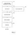
- FIG. 2is a process flow diagram illustrating an exemplary process by which semiconductor devices are fabricated using the apparatus shown in FIG. 1 according to the invention
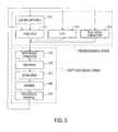
- FIG. 3is a flowchart of the wafer processing step shown in FIG. 2 in the case of fabricating semiconductor devices according to the invention
- FIG. 4is a schematic side cross-sectional view of an autofocus unit embodying this invention.
- FIG. 5is a schematic side cross-sectional view of another autofocus unit embodying this invention.
- FIG. 6is an enlarged view of a circled portion 6 of FIG. 5 ;
- FIGS. 7 , 8 and 9are schematic side cross-sectional views of portions of other autofocus units embodying this invention according to different embodiment of the invention.
- FIG. 1shows the general structure of an immersion lithography apparatus 100 that may incorporate the optical arrangement of autofocus elements embodying this invention.
- the immersion lithography apparatus 100comprises an illuminator optical unit 1 including a light source such as a KrF excimer laser unit, an optical integrator (or homogenizer) and a lens and serving to emit pulsed ultraviolet light IL with wavelength 248 nm to be made incident to a pattern on a reticle R.
- the pattern on the reticle Ris projected onto a wafer W coated with a photoresist at a specified magnification (such as 1 ⁇ 4 or 1 ⁇ 5) through a telecentric light projection unit PL.
- the pulsed light ILmay alternatively be ArF excimer laser light with wavelength 193 nm, F 2 laser light with wavelength 157 nm or the i-line of a mercury lamp with wavelength 365 nm.
- the coordinate system with X-, Y- and Z-axes as shown in FIG. 1is referenced to explain the directions in describing the structure and functions of the lithography apparatus 100 .
- the light projection unit PLis illustrated in FIG. 1 only by way of its last-stage optical element (such as a lens) 4 disposed opposite to the wafer W and a cylindrical housing 3 containing all others of its components.
- the reticle Ris supported on a reticle stage RST incorporating a mechanism for moving the reticle R by some amount in the X-direction, the Y-direction and the rotary direction around the Z-axis.
- the two-dimensional position and orientation of the reticle R on the reticle stage RSTare detected by a laser interferometer (not shown) in real time and the positioning of the reticle R is affected by a main control unit 14 on the basis of the detection thus made.
- the wafer Wis set on a wafer holder (not shown) on a Z-stage 9 for controlling the focusing position (along the Z-axis) and the sloping angle of the wafer W.
- the Z-stage 9is affixed to an XY-stage 10 adapted to move in the XY-plane substantially parallel to the image-forming surface of the light projection unit PL.
- the XY-stage 10is set on a base 11 .
- the Z-stage 9serves to match the wafer surface with the image surface of the light projection unit PL by adjusting the focusing position (along the Z-axis) and the sloping angle of the wafer W by the auto-focusing and auto-leveling method
- the XY-stage 10serves to adjust the position of the wafer W in the X-direction and the Y-direction.
- the two-dimensional position and orientation of the Z-stage 9(and hence also of the wafer W) are monitored in real time by another laser interferometer 13 with reference to a mobile mirror 12 affixed to the Z-stage 9 .
- Control data based on the results of this monitoringare transmitted from the main control unit 14 to a stage-driving unit 15 adapted to control the motions of the Z-stage 9 and the XY-stage 10 according to the received control data.
- the projection lightis made to sequentially move from one to another of different exposure positions on the wafer W according to the pattern on the reticle R in a step-and-repeat routine.
- the lithography apparatus 100 described with reference to FIG. 1is an immersion lithography apparatus and is hence adapted to have a liquid (or the “immersion liquid”) 7 of a specified kind such as water filling the space between the surface of the wafer W and the lower surface of the last-stage optical element 4 of the light projection unit PL at least while the pattern image of the reticle R is being copied onto the wafer W.
- a liquid (or the “immersion liquid”) 7 of a specified kindsuch as water filling the space between the surface of the wafer W and the lower surface of the last-stage optical element 4 of the light projection unit PL at least while the pattern image of the reticle R is being copied onto the wafer W.
- the last-stage optical element 4 of the light projection unit PLis affixed to the cylindrical housing 3 .
- the last-stage optical element 4may be made removable for cleaning or maintenance.
- the liquid 7is supplied from a liquid supply unit 5 that may comprise a tank, a pressure pump and a temperature regulator (not individually shown) to the space above the wafer W under a temperature-regulated condition and is collected by a liquid recovery unit 6 .
- the temperature of the liquid 7is regulated to be approximately the same as the temperature inside the chamber in which the lithography apparatus 100 itself is disposed.
- Numeral 21indicates source nozzles through which the liquid 7 is supplied from the supply unit 5 .
- Numeral 23indicates recovery nozzles through which the liquid 7 is collected into the recovery unit 6 .
- autofocus units of the inventionmay be incorporated into immersion lithography apparatus of many different kinds.
- the numbers and arrangements of the source and recovery nozzles 21 and 23 around the light projection unit PLmay be designed in a variety of ways for establishing a smooth flow and quick recovery of the immersion liquid 7 .
- FIG. 4shows an autofocus unit 50 (not shown in FIG. 1 ) according to this invention which may be incorporated into an immersion lithography system such as shown at 100 in FIG. 1 , but the invention is not intended to be limited by the specific type of the system into which it is incorporated.
- the last-stage optical element 4 of the light projection unit PLis a hemispherically shaped projection lens with its planar surface facing downward opposite to the upper surface (the “target surface”) of the wafer W, with a space left in between.
- An autofocus light source 51is arranged such that its AF/AL light beam 54 , emitted obliquely with respect to the target surface of the wafer W, passes through a lower peripheral part of this lens 4 and then is refracted into the immersion liquid 7 so as to be reflected by the target surface of the wafer W at a specified reflection position 55 .
- a receiver 52 for receiving and analyzing the reflected AF/AL light beam 54is appropriately positioned on the opposite side of the light projection unit PL.
- Numerals 53each indicate what may be referred to as a correction lens disposed on the path of the AF/AL light beam 54 for correcting light propagation. Since the interface between the lens 4 and the liquid 7 is well defined and essentially free of bubbles, the light beams are unimpeded and can provide good signals to maintain high accuracy.
- broken linesindicate the exposure light cone, or the boundary of the exposure region.
- FIG. 5shows another autofocus unit 60 according to another embodiment of the invention. Its components that are similar to those described above with reference to FIG. 5 are indicated by the same numerals.
- the unit 60 shown in FIG. 5is characterized as having the lower surface of the last-stage optical element 4 of the light projection unit PL cut in two places facing respectively the autofocus light source 51 and the receiver 52 .
- the cut surfacespreferably may be flat, as shown in FIG. 5 , and the last-stage optical element 4 is still functionally and essentially a hemispherical lens.
- Optically transparent partsreferred to as wedge elements 61 and 62 , are placed on both sides of the lens 4 under these cut surfaces, the element 61 being on the side of the autofocus light source 51 and the element 62 being on the side of the receiver 52 .
- the cuts and the wedge elements 61 and 62are designed so that the AF/AL light beam 54 from the autofocus light source 51 will pass through the wedge element 61 and be refracted into the immersion liquid 7 without passing through the lens 4 and, after being reflected by the target surface of the wafer W at the reflection position 55 , will be refracted into the wedge element 62 and received by the receiver 52 again without passing through the lens 4 .
- This embodimentis advantageous because the wedge elements can be made of a different material from the lens element 4 , such as optical glass.
- the lower interface between the wedge elements 61 and 62 and the lens 4is important from the points of view of correct optical performance and generation of bubbles in the immersion liquid 7 .
- FIG. 6which shows in more detail the portion of the wedge element 61 in a close proximity of the lens 4 , the gap D therebetween is a potential source of air bubbles, which may be entrained under the lens 4 , adversely affecting its optical performance.
- One of the solutions to this problemis to fill the gap with a suitable material or to press the wedge element 61 into contact with the lens 4 such that the gap D becomes effectively zero and therefore does not perturb the liquid interface.
- Another solutionis to keep D approximately equal to or less than 2.0 mm such that capillary forces cause the liquid 7 to fill the gap and keep it filled even while the wafer W is moved under the lens 4 .
- a third solutionis to supply a small suction to cause the liquid 7 to move up inside the gap D and to prevent air from moving downward, as shown in FIG. 7 in which numeral 70 indicates an air pump for providing the suction.
- FIG. 8shows still another solution whereby a source 72 of the liquid 7 is supplied above the opening of the gap D to keep the gap D filled with the liquid 7 .
- the shape of the wedge elements 61 and 62need not be as described above with reference to FIG. 6 .
- Thiswill provide flexibility in the design of the arrangement embodying this invention.
- FIG. 2is referenced next to describe a process for fabricating a semiconductor device by using an immersion lithography apparatus incorporating a liquid jet and recovery system embodying this invention.
- step 301the device's function and performance characteristics are designed.
- step 302a mask (reticle) having a pattern is designed according to the previous designing step, and in a parallel step 303 , a wafer is made from a silicon material.
- the mask pattern designed in step 302is exposed onto the wafer from step 303 in step 304 by a photolithography system such as the systems described above.
- step 305the semiconductor device is assembled (including the dicing process, bonding process and packaging process), then finally the device is inspected in step 306 .
- FIG. 3illustrates a detailed flowchart example of the above-mentioned step 304 in the case of fabricating semiconductor devices.
- step 311oxidation step
- step 312CVD step
- step 313electrode formation step
- step 314ion implantation step
- ionsare implanted in the wafer.
- the aforementioned steps 311 - 314form the preprocessing steps for wafers during wafer processing, and selection is made at each step according to processing requirements.
- step 315photoresist formation step
- step 316exposure step
- step 317developing step
- step 318etching step
- steps other than residual photoresistexposed material surface
- step 319photoresist removal step
Landscapes
- General Physics & Mathematics (AREA)
- Physics & Mathematics (AREA)
- Engineering & Computer Science (AREA)
- Public Health (AREA)
- Environmental & Geological Engineering (AREA)
- Epidemiology (AREA)
- Health & Medical Sciences (AREA)
- Condensed Matter Physics & Semiconductors (AREA)
- Manufacturing & Machinery (AREA)
- Computer Hardware Design (AREA)
- Microelectronics & Electronic Packaging (AREA)
- Power Engineering (AREA)
- Exposure Of Semiconductors, Excluding Electron Or Ion Beam Exposure (AREA)
- Exposure And Positioning Against Photoresist Photosensitive Materials (AREA)
- Automatic Focus Adjustment (AREA)
Abstract
Description
This is a Divisional of U.S. patent application Ser. No. 12/461,762 filed Aug. 24, 2009, which in turn is a Divisional of U.S. patent application Ser. No. 12/457,742 filed Jun. 19, 2009 (now U.S. Pat. No. 8,018,657), which in turn is a Divisional of U.S. patent application Ser. No. 11/606,914 filed Dec. 1, 2006 (now U.S. Pat. No. 7,570,431), which in turn is a Divisional of U.S. patent application Ser. No. 11/234,279 filed Sep. 26, 2005 (now U.S. Pat. No. 7,414,794), which in turn is a Continuation of International Application No. PCT/US2004/011287 filed Apr. 12, 2004, which claims the benefit of U.S. Provisional Patent Application No. 60/464,392 filed Apr. 17, 2003. The disclosures of the above-identified applications are incorporated by reference herein in their entireties.
This invention relates to an optical arrangement of autofocus elements for use with immersion lithography.
In semiconductor lithography systems in use today, automatic focusing and leveling (AF/AL) is typically accomplished by passing a low angle of incidence optical beam onto the surface of a silicon wafer and detecting its properties after subsequent reflection from the wafer surface. The wafer height is determined by optical and electrical processing of the reflected light beam. This beam passes under the last element of the projection lens. The source and receiver optics are typically mounted to a stable part of the system, close to the projection optics mounting position.
In immersion lithography, a liquid such as water fills the space between the last surface of the projection lens and the wafer. At the edge of the water, typically at the edge of the lens or supported structure near the edge of the lens, the liquid-air boundary is not well defined and is changing rapidly. It is not possible to transmit an AF/AL beam through this interface without substantial disruption and subsequent loss of signal, and hence performance.
It is therefore a general object of this invention to provide a way to introduce AF/AL beams into the liquid layer without such disruption so as to preserve the optical accuracy and stability required.
More specifically, it is an object of this invention to provide an apparatus and a method for allowing AF/AL light beams to be used as in conventional lithography without the disrupting influence of the liquid immersion boundary at the edge of the lens.
Autofocus units according to this invention are for an immersion lithography apparatus that may be described generally as comprising a reticle stage arranged to retain a reticle, a working stage arranged to retain a workpiece having a target surface, an optical system including an illumination source and an optical element such as a lens positioned opposite and above the workpiece for projecting an image pattern of the reticle onto the workpiece by radiation from the illumination source, and a fluid-supplying device for providing a fluid into the space defined between the optical element and the workpiece such that the fluid contacts both the optical element and the target surface of the workpiece. The optical element positioned opposite to the workpiece may be treated as a component of the autofocus unit itself which may be characterized as further comprising an autofocus light source serving to project a light beam obliquely at a specified angle such that this light beam passes through the fluid and is reflected by the target surface of the workpiece at a specified reflection position that is below the optical element, and a receiver for receiving and analyzing the light beam reflected by the target surface. Correction lenses preferably may be disposed on the optical path of the light beam projected from the autofocus light source for correcting propagation of the light beam.
As an alternative embodiment, the optical element opposite the workpiece may be cut on its two mutually opposite sides, and optically transparent wedge-shaped elements may be placed under these cuts such that the light beam from the autofocus light source will pass through them as it is passed through the fluid to be reflected on the target surface of the workpiece and to reach the receiver without passing through the optical element at all. In order to cope with the potential problem of bubbles that may be formed due to the gap between the wedge element and the optical element, the gap may be filled with a suitable material, made sufficiently narrow such as less than 2.0 mm such that capillary forces will keep the gap filled with the fluid, or provided with means for supplying a small suction to cause the fluid to move up through the gap or to supply the fluid such that the gap can be kept filled. The boundary surface through which the light beam from the autofocus light source is refracted into the fluid from the interior of the wedge element need not be parallel to the target surface of the workpiece, but may be appropriately sloped, depending on the indices of refraction of the materials that affect the design of the unit.
The invention will be described in conjunction with the accompanying drawings of exemplary embodiments in which like reference numerals designate like elements, and in which:
As shown inFIG. 1 , theimmersion lithography apparatus 100 comprises an illuminatoroptical unit 1 including a light source such as a KrF excimer laser unit, an optical integrator (or homogenizer) and a lens and serving to emit pulsed ultraviolet light IL with wavelength 248 nm to be made incident to a pattern on a reticle R. The pattern on the reticle R is projected onto a wafer W coated with a photoresist at a specified magnification (such as ¼ or ⅕) through a telecentric light projection unit PL. The pulsed light IL may alternatively be ArF excimer laser light with wavelength 193 nm, F2laser light with wavelength 157 nm or the i-line of a mercury lamp with wavelength 365 nm. In what follows, the coordinate system with X-, Y- and Z-axes as shown inFIG. 1 is referenced to explain the directions in describing the structure and functions of thelithography apparatus 100. For the convenience of disclosure and description, the light projection unit PL is illustrated inFIG. 1 only by way of its last-stage optical element (such as a lens)4 disposed opposite to the wafer W and acylindrical housing 3 containing all others of its components.
The reticle R is supported on a reticle stage RST incorporating a mechanism for moving the reticle R by some amount in the X-direction, the Y-direction and the rotary direction around the Z-axis. The two-dimensional position and orientation of the reticle R on the reticle stage RST are detected by a laser interferometer (not shown) in real time and the positioning of the reticle R is affected by amain control unit 14 on the basis of the detection thus made.
The wafer W is set on a wafer holder (not shown) on a Z-stage 9 for controlling the focusing position (along the Z-axis) and the sloping angle of the wafer W. The Z-stage 9 is affixed to an XY-stage 10 adapted to move in the XY-plane substantially parallel to the image-forming surface of the light projection unit PL. The XY-stage 10 is set on abase 11. Thus, the Z-stage 9 serves to match the wafer surface with the image surface of the light projection unit PL by adjusting the focusing position (along the Z-axis) and the sloping angle of the wafer W by the auto-focusing and auto-leveling method, and the XY-stage 10 serves to adjust the position of the wafer W in the X-direction and the Y-direction.
The two-dimensional position and orientation of the Z-stage9 (and hence also of the wafer W) are monitored in real time by anotherlaser interferometer 13 with reference to amobile mirror 12 affixed to the Z-stage 9. Control data based on the results of this monitoring are transmitted from themain control unit 14 to a stage-drivingunit 15 adapted to control the motions of the Z-stage 9 and the XY-stage 10 according to the received control data. At the time of an exposure, the projection light is made to sequentially move from one to another of different exposure positions on the wafer W according to the pattern on the reticle R in a step-and-repeat routine.
Thelithography apparatus 100 described with reference toFIG. 1 is an immersion lithography apparatus and is hence adapted to have a liquid (or the “immersion liquid”)7 of a specified kind such as water filling the space between the surface of the wafer W and the lower surface of the last-stageoptical element 4 of the light projection unit PL at least while the pattern image of the reticle R is being copied onto the wafer W.
The last-stageoptical element 4 of the light projection unit PL is affixed to thecylindrical housing 3. In an optional embodiment, the last-stageoptical element 4 may be made removable for cleaning or maintenance.
Theliquid 7 is supplied from aliquid supply unit 5 that may comprise a tank, a pressure pump and a temperature regulator (not individually shown) to the space above the wafer W under a temperature-regulated condition and is collected by aliquid recovery unit 6. The temperature of theliquid 7 is regulated to be approximately the same as the temperature inside the chamber in which thelithography apparatus 100 itself is disposed.Numeral 21 indicates source nozzles through which theliquid 7 is supplied from thesupply unit 5.Numeral 23 indicates recovery nozzles through which theliquid 7 is collected into therecovery unit 6. The structure described above with reference toFIG. 1 is not intended to limit the scope of the immersion lithography apparatus to which the methods and devices of the invention are applicable. In other words, autofocus units of the invention may be incorporated into immersion lithography apparatus of many different kinds. In particular, the numbers and arrangements of the source andrecovery nozzles immersion liquid 7.
The lower interface between thewedge elements lens 4 is important from the points of view of correct optical performance and generation of bubbles in theimmersion liquid 7. With reference toFIG. 6 , which shows in more detail the portion of thewedge element 61 in a close proximity of thelens 4, the gap D therebetween is a potential source of air bubbles, which may be entrained under thelens 4, adversely affecting its optical performance.
One of the solutions to this problem is to fill the gap with a suitable material or to press thewedge element 61 into contact with thelens 4 such that the gap D becomes effectively zero and therefore does not perturb the liquid interface. Another solution is to keep D approximately equal to or less than 2.0 mm such that capillary forces cause theliquid 7 to fill the gap and keep it filled even while the wafer W is moved under thelens 4. A third solution is to supply a small suction to cause theliquid 7 to move up inside the gap D and to prevent air from moving downward, as shown inFIG. 7 in whichnumeral 70 indicates an air pump for providing the suction.FIG. 8 shows still another solution whereby asource 72 of theliquid 7 is supplied above the opening of the gap D to keep the gap D filled with theliquid 7.
The invention has been described above with reference to only a limited number of arrangements, but they are not intended to limit the scope of the invention. Many modifications and variations are possible within the scope of the invention. The shape of thewedge elements FIG. 6 . Depending, for example, upon the desired angle of incidence of the AF/AL light beam 54 relative to the indices of refraction of theimmersion liquid 7 and the material of thewedge element 61, it may be advantageous, as shown inFIG. 9 , to provide thewedge element 61 with asloped surface portion 64 such that the AF/AL light beam 54 passing through thewedge element 61 will be refracted into theimmersion liquid 7, not necessarily through a horizontal boundary surface as shown inFIG. 6 , but through this appropriately slopedsurface portion 64. This will provide flexibility in the design of the arrangement embodying this invention.
At each stage of wafer processing, when the above-mentioned preprocessing steps have been completed, the following post-processing steps are implemented. During post-processing, initially, in step315 (photoresist formation step), photoresist is applied to a wafer. Next, in step316 (exposure step), the above-mentioned exposure device is used to transfer the circuit pattern of a mask (reticle) onto a wafer. Then, in step317 (developing step), the exposed wafer is developed, and in step318 (etching step), parts other than residual photoresist (exposed material surface) are removed by etching. In step319 (photoresist removal step), unnecessary photoresist remaining after etching is removed. Multiple circuit patterns are formed by repetition of these preprocessing and post-processing steps.
While a lithography system of this invention has been described in terms of several preferred embodiments, there are alterations, permutations, and various substitute equivalents that fall within the scope of this invention. There are many alternative ways of implementing the methods and apparatus of the invention.
Claims (25)
1. A lithographic projection apparatus comprising:
a projection system having a spherical lens element from which an exposure light is projected through liquid in a space under the spherical lens element;
a member disposed adjacent to a surface of the spherical lens element through which the exposure light does not pass; and
a gap formed between the member and the surface of the spherical lens element, the gap being in fluidic communication with the space, the gap including a lower portion and an upper portion between which the gap extends,
wherein
a wafer is moved below and relative to the spherical lens element and the member;
the liquid is retained between the spherical lens element and the member on one side and an upper surface of the wafer on the other side; and
the liquid locally covers a portion of the upper surface of the wafer to expose the wafer by projecting the exposure light onto the wafer through the liquid in the space.
2. The apparatus according toclaim 1 , wherein the upper surface of the wafer faces an undersurface of the member.
3. The apparatus according toclaim 1 , wherein the spherical lens element has a planar undersurface which is substantially co-planar with an undersurface of the member.
4. The apparatus according toclaim 1 , wherein the gap is formed between the surface of the spherical lens element and an opposing surface of the member, the opposing surface including a first surface and a second surface which are not parallel to each other, and the first surface being located below and adjacent to the second surface.
5. The apparatus according toclaim 4 , wherein the second surface of the opposing surface extends upwardly from an upper end of the first surface and extends outwardly from the upper end of the first surface with respect to the spherical lens element.
6. The apparatus according toclaim 4 , wherein the upper surface of the wafer faces a planar undersurface of the spherical lens element.
7. The apparatus according toclaim 4 , wherein the surface of the spherical lens element forming the gap includes a side surface of the spherical lens element.
8. The apparatus according toclaim 4 , wherein the gap extends upwardly from the lower portion toward the upper portion and extends outwardly from the lower portion toward the upper portion with respect to the spherical lens element.
9. The apparatus according toclaim 4 , wherein the gap is formed such that the gap generates a capillary force.
10. The apparatus according toclaim 4 , wherein a size of the gap is approximately equal to or less than 2.0 mm.
11. The apparatus according toclaim 4 , wherein suction is provided to the gap.
12. The apparatus according toclaim 11 , wherein the liquid is moved up in the gap.
13. The apparatus according toclaim 11 , wherein the suction is provided using a pump.
14. The apparatus according toclaim 4 , wherein liquid is supplied to the gap.
15. The apparatus according toclaim 14 , wherein a liquid source is provided above an opening of the gap.
16. The apparatus according toclaim 1 , wherein the upper surface of the wafer faces a planar undersurface of the spherical lens element.
17. The apparatus according toclaim 1 , wherein the surface of the spherical lens element forming the gap includes a side surface of the spherical lens element.
18. The apparatus according toclaim 1 , wherein the gap extends upwardly from the lower portion toward the upper portion and extends outwardly from the lower portion toward the upper portion with respect to the spherical lens element.
19. The apparatus according toclaim 1 , wherein the gap is formed such that the gap generates a capillary force.
20. The apparatus according toclaim 1 , wherein a size of the gap is approximately equal to or less than 2.0 mm.
21. The apparatus according toclaim 1 , wherein suction is provided to the gap.
22. The apparatus according toclaim 21 , wherein the liquid is moved up in the gap.
23. The apparatus according toclaim 21 , wherein the suction is provided using a pump.
24. The apparatus according toclaim 1 , wherein liquid is supplied to the gap.
25. The apparatus according toclaim 24 , wherein a liquid source is provided above an opening of the gap.
Priority Applications (4)
| Application Number | Priority Date | Filing Date | Title |
|---|---|---|---|
| US13/313,399US8599488B2 (en) | 2003-04-17 | 2011-12-07 | Optical arrangement of autofocus elements for use with immersion lithography |
| US14/066,315US8810915B2 (en) | 2003-04-17 | 2013-10-29 | Optical arrangement of autofocus elements for use with immersion lithography |
| US14/330,263US8953250B2 (en) | 2003-04-17 | 2014-07-14 | Optical arrangement of autofocus elements for use with immersion lithography |
| US14/589,399US9086636B2 (en) | 2003-04-17 | 2015-01-05 | Optical arrangement of autofocus elements for use with immersion lithography |
Applications Claiming Priority (7)
| Application Number | Priority Date | Filing Date | Title |
|---|---|---|---|
| US46439203P | 2003-04-17 | 2003-04-17 | |
| PCT/US2004/011287WO2004095135A2 (en) | 2003-04-17 | 2004-04-12 | Optical arrangement of autofocus elements for use with immersion lithography |
| US11/234,279US7414794B2 (en) | 2003-04-17 | 2005-09-26 | Optical arrangement of autofocus elements for use with immersion lithography |
| US11/606,914US7570431B2 (en) | 2003-04-17 | 2006-12-01 | Optical arrangement of autofocus elements for use with immersion lithography |
| US12/457,742US8018657B2 (en) | 2003-04-17 | 2009-06-19 | Optical arrangement of autofocus elements for use with immersion lithography |
| US12/461,762US8094379B2 (en) | 2003-04-17 | 2009-08-24 | Optical arrangement of autofocus elements for use with immersion lithography |
| US13/313,399US8599488B2 (en) | 2003-04-17 | 2011-12-07 | Optical arrangement of autofocus elements for use with immersion lithography |
Related Parent Applications (1)
| Application Number | Title | Priority Date | Filing Date |
|---|---|---|---|
| US12/461,762DivisionUS8094379B2 (en) | 2003-04-17 | 2009-08-24 | Optical arrangement of autofocus elements for use with immersion lithography |
Related Child Applications (1)
| Application Number | Title | Priority Date | Filing Date |
|---|---|---|---|
| US14/066,315DivisionUS8810915B2 (en) | 2003-04-17 | 2013-10-29 | Optical arrangement of autofocus elements for use with immersion lithography |
Publications (2)
| Publication Number | Publication Date |
|---|---|
| US20120075609A1 US20120075609A1 (en) | 2012-03-29 |
| US8599488B2true US8599488B2 (en) | 2013-12-03 |
Family
ID=33310880
Family Applications (8)
| Application Number | Title | Priority Date | Filing Date |
|---|---|---|---|
| US11/234,279Expired - Fee RelatedUS7414794B2 (en) | 2003-04-17 | 2005-09-26 | Optical arrangement of autofocus elements for use with immersion lithography |
| US11/606,914Expired - Fee RelatedUS7570431B2 (en) | 2003-04-17 | 2006-12-01 | Optical arrangement of autofocus elements for use with immersion lithography |
| US12/457,742Expired - Fee RelatedUS8018657B2 (en) | 2003-04-17 | 2009-06-19 | Optical arrangement of autofocus elements for use with immersion lithography |
| US12/461,762Expired - Fee RelatedUS8094379B2 (en) | 2003-04-17 | 2009-08-24 | Optical arrangement of autofocus elements for use with immersion lithography |
| US13/313,399Expired - Fee RelatedUS8599488B2 (en) | 2003-04-17 | 2011-12-07 | Optical arrangement of autofocus elements for use with immersion lithography |
| US14/066,315Expired - Fee RelatedUS8810915B2 (en) | 2003-04-17 | 2013-10-29 | Optical arrangement of autofocus elements for use with immersion lithography |
| US14/330,263Expired - Fee RelatedUS8953250B2 (en) | 2003-04-17 | 2014-07-14 | Optical arrangement of autofocus elements for use with immersion lithography |
| US14/589,399Expired - Fee RelatedUS9086636B2 (en) | 2003-04-17 | 2015-01-05 | Optical arrangement of autofocus elements for use with immersion lithography |
Family Applications Before (4)
| Application Number | Title | Priority Date | Filing Date |
|---|---|---|---|
| US11/234,279Expired - Fee RelatedUS7414794B2 (en) | 2003-04-17 | 2005-09-26 | Optical arrangement of autofocus elements for use with immersion lithography |
| US11/606,914Expired - Fee RelatedUS7570431B2 (en) | 2003-04-17 | 2006-12-01 | Optical arrangement of autofocus elements for use with immersion lithography |
| US12/457,742Expired - Fee RelatedUS8018657B2 (en) | 2003-04-17 | 2009-06-19 | Optical arrangement of autofocus elements for use with immersion lithography |
| US12/461,762Expired - Fee RelatedUS8094379B2 (en) | 2003-04-17 | 2009-08-24 | Optical arrangement of autofocus elements for use with immersion lithography |
Family Applications After (3)
| Application Number | Title | Priority Date | Filing Date |
|---|---|---|---|
| US14/066,315Expired - Fee RelatedUS8810915B2 (en) | 2003-04-17 | 2013-10-29 | Optical arrangement of autofocus elements for use with immersion lithography |
| US14/330,263Expired - Fee RelatedUS8953250B2 (en) | 2003-04-17 | 2014-07-14 | Optical arrangement of autofocus elements for use with immersion lithography |
| US14/589,399Expired - Fee RelatedUS9086636B2 (en) | 2003-04-17 | 2015-01-05 | Optical arrangement of autofocus elements for use with immersion lithography |
Country Status (8)
| Country | Link |
|---|---|
| US (8) | US7414794B2 (en) |
| EP (1) | EP1614000B1 (en) |
| JP (2) | JP2006523958A (en) |
| KR (2) | KR20050122269A (en) |
| CN (1) | CN1774667A (en) |
| AT (1) | ATE542167T1 (en) |
| SG (2) | SG194246A1 (en) |
| WO (1) | WO2004095135A2 (en) |
Cited By (1)
| Publication number | Priority date | Publication date | Assignee | Title |
|---|---|---|---|---|
| US8810915B2 (en) | 2003-04-17 | 2014-08-19 | Nikon Corporation | Optical arrangement of autofocus elements for use with immersion lithography |
Families Citing this family (145)
| Publication number | Priority date | Publication date | Assignee | Title |
|---|---|---|---|---|
| TWI249082B (en)* | 2002-08-23 | 2006-02-11 | Nikon Corp | Projection optical system and method for photolithography and exposure apparatus and method using same |
| CN100568101C (en) | 2002-11-12 | 2009-12-09 | Asml荷兰有限公司 | Photolithography apparatus and device manufacturing method |
| SG121822A1 (en) | 2002-11-12 | 2006-05-26 | Asml Netherlands Bv | Lithographic apparatus and device manufacturing method |
| US9482966B2 (en) | 2002-11-12 | 2016-11-01 | Asml Netherlands B.V. | Lithographic apparatus and device manufacturing method |
| US7372541B2 (en) | 2002-11-12 | 2008-05-13 | Asml Netherlands B.V. | Lithographic apparatus and device manufacturing method |
| US10503084B2 (en) | 2002-11-12 | 2019-12-10 | Asml Netherlands B.V. | Lithographic apparatus and device manufacturing method |
| KR100585476B1 (en) | 2002-11-12 | 2006-06-07 | 에이에스엠엘 네델란즈 비.브이. | Lithographic Apparatus and Device Manufacturing Method |
| US7948604B2 (en) | 2002-12-10 | 2011-05-24 | Nikon Corporation | Exposure apparatus and method for producing device |
| EP1571694A4 (en) | 2002-12-10 | 2008-10-15 | Nikon Corp | Exposure apparatus and method for manufacturing device |
| KR20120127755A (en) | 2002-12-10 | 2012-11-23 | 가부시키가이샤 니콘 | Exposure apparatus and method for manufacturing device |
| US7242455B2 (en) | 2002-12-10 | 2007-07-10 | Nikon Corporation | Exposure apparatus and method for producing device |
| WO2004053955A1 (en) | 2002-12-10 | 2004-06-24 | Nikon Corporation | Exposure system and device producing method |
| JP4352874B2 (en) | 2002-12-10 | 2009-10-28 | 株式会社ニコン | Exposure apparatus and device manufacturing method |
| KR101101737B1 (en) | 2002-12-10 | 2012-01-05 | 가부시키가이샤 니콘 | Exposure apparatus, exposure method and method for manufacturing device |
| DE10261775A1 (en) | 2002-12-20 | 2004-07-01 | Carl Zeiss Smt Ag | Device for the optical measurement of an imaging system |
| EP2466623B1 (en) | 2003-02-26 | 2015-04-22 | Nikon Corporation | Exposure apparatus, exposure method, and method for producing device |
| KR20050110033A (en) | 2003-03-25 | 2005-11-22 | 가부시키가이샤 니콘 | Exposure system and device production method |
| EP1612850B1 (en) | 2003-04-07 | 2009-03-25 | Nikon Corporation | Exposure apparatus and method for manufacturing a device |
| WO2004093159A2 (en) | 2003-04-09 | 2004-10-28 | Nikon Corporation | Immersion lithography fluid control system |
| EP3062152B1 (en) | 2003-04-10 | 2017-12-20 | Nikon Corporation | Environmental system including vaccum scavenge for an immersion lithography apparatus |
| EP2950147B1 (en) | 2003-04-10 | 2017-04-26 | Nikon Corporation | Environmental system including vaccum scavenge for an immersion lithography apparatus |
| EP3352010A1 (en) | 2003-04-10 | 2018-07-25 | Nikon Corporation | Run-off path to collect liquid for an immersion lithography apparatus |
| JP4582089B2 (en) | 2003-04-11 | 2010-11-17 | 株式会社ニコン | Liquid jet recovery system for immersion lithography |
| KR101225884B1 (en) | 2003-04-11 | 2013-01-28 | 가부시키가이샤 니콘 | Apparatus and method for maintaining immersion fluid in the gap under the projection lens during wafer exchange in an immersion lithography machine |
| CN101825847B (en) | 2003-04-11 | 2013-10-16 | 株式会社尼康 | Cleanup method for optics in immersion lithography |
| EP2722703A3 (en) | 2003-05-06 | 2014-07-23 | Nikon Corporation | Projection optical system, and exposure apparatus and exposure method |
| US7348575B2 (en) | 2003-05-06 | 2008-03-25 | Nikon Corporation | Projection optical system, exposure apparatus, and exposure method |
| TWI295414B (en)* | 2003-05-13 | 2008-04-01 | Asml Netherlands Bv | Lithographic apparatus and device manufacturing method |
| KR20060009356A (en) | 2003-05-15 | 2006-01-31 | 가부시키가이샤 니콘 | Exposure apparatus and device manufacturing method |
| TWI421906B (en) | 2003-05-23 | 2014-01-01 | 尼康股份有限公司 | An exposure method, an exposure apparatus, and an element manufacturing method |
| TW201806001A (en) | 2003-05-23 | 2018-02-16 | 尼康股份有限公司 | Exposure device and device manufacturing method |
| KR101548832B1 (en) | 2003-05-28 | 2015-09-01 | 가부시키가이샤 니콘 | Exposure method, exposure device, and device manufacturing method |
| US7213963B2 (en) | 2003-06-09 | 2007-05-08 | Asml Netherlands B.V. | Lithographic apparatus and device manufacturing method |
| US7317504B2 (en) | 2004-04-08 | 2008-01-08 | Asml Netherlands B.V. | Lithographic apparatus and device manufacturing method |
| EP2261741A3 (en) | 2003-06-11 | 2011-05-25 | ASML Netherlands B.V. | Lithographic apparatus and device manufacturing method |
| KR101242815B1 (en) | 2003-06-13 | 2013-03-12 | 가부시키가이샤 니콘 | Exposure method, substrate stage, exposure apparatus and method for manufacturing device |
| US6867844B2 (en) | 2003-06-19 | 2005-03-15 | Asml Holding N.V. | Immersion photolithography system and method using microchannel nozzles |
| TW201721717A (en) | 2003-06-19 | 2017-06-16 | 尼康股份有限公司 | Exposure apparatus, exposure method, and device manufacturing method |
| US6809794B1 (en) | 2003-06-27 | 2004-10-26 | Asml Holding N.V. | Immersion photolithography system and method using inverted wafer-projection optics interface |
| EP1491956B1 (en) | 2003-06-27 | 2006-09-06 | ASML Netherlands B.V. | Lithographic apparatus and device manufacturing method |
| KR20060027832A (en) | 2003-07-01 | 2006-03-28 | 가부시키가이샤 니콘 | Method of Using Isotopically Specified Fluids as Optical Elements |
| EP3179309A1 (en) | 2003-07-08 | 2017-06-14 | Nikon Corporation | Wafer table for immersion lithography |
| EP1643543B1 (en) | 2003-07-09 | 2010-11-24 | Nikon Corporation | Exposure apparatus and method for manufacturing device |
| WO2005006418A1 (en) | 2003-07-09 | 2005-01-20 | Nikon Corporation | Exposure apparatus and method for manufacturing device |
| WO2005006415A1 (en) | 2003-07-09 | 2005-01-20 | Nikon Corporation | Exposure apparatus and method for manufacturing device |
| WO2005010960A1 (en) | 2003-07-25 | 2005-02-03 | Nikon Corporation | Inspection method and inspection device for projection optical system, and production method for projection optical system |
| EP1503244A1 (en) | 2003-07-28 | 2005-02-02 | ASML Netherlands B.V. | Lithographic projection apparatus and device manufacturing method |
| US7326522B2 (en) | 2004-02-11 | 2008-02-05 | Asml Netherlands B.V. | Device manufacturing method and a substrate |
| KR101641011B1 (en) | 2003-07-28 | 2016-07-19 | 가부시키가이샤 니콘 | Exposure apparatus, device producing method, and exposure apparatus controlling method |
| US7175968B2 (en) | 2003-07-28 | 2007-02-13 | Asml Netherlands B.V. | Lithographic apparatus, device manufacturing method and a substrate |
| US7779781B2 (en) | 2003-07-31 | 2010-08-24 | Asml Netherlands B.V. | Lithographic apparatus and device manufacturing method |
| TWI263859B (en) | 2003-08-29 | 2006-10-11 | Asml Netherlands Bv | Lithographic apparatus and device manufacturing method |
| EP2261740B1 (en) | 2003-08-29 | 2014-07-09 | ASML Netherlands BV | Lithographic apparatus |
| KR101380989B1 (en) | 2003-08-29 | 2014-04-04 | 가부시키가이샤 니콘 | Exposure apparatus and device producing method |
| EP3223053A1 (en) | 2003-09-03 | 2017-09-27 | Nikon Corporation | Apparatus and method for providing fluid for immersion lithography |
| JP4444920B2 (en) | 2003-09-19 | 2010-03-31 | 株式会社ニコン | Exposure apparatus and device manufacturing method |
| EP2837969B1 (en) | 2003-09-29 | 2016-04-20 | Nikon Corporation | Exposure apparatus, exposure method, and method for producing device |
| JP2005136364A (en) | 2003-10-08 | 2005-05-26 | Zao Nikon Co Ltd | Substrate transport apparatus, exposure apparatus, and device manufacturing method |
| KR101203028B1 (en) | 2003-10-08 | 2012-11-21 | 가부시키가이샤 자오 니콘 | Substrate carrying apparatus, substrate carrying method, exposure apparatus, exposure method, and method for producing device |
| KR20060126949A (en) | 2003-10-08 | 2006-12-11 | 가부시키가이샤 니콘 | Substrate conveyance apparatus and substrate conveyance method, exposure apparatus, exposure method, and device manufacturing method |
| TWI553701B (en) | 2003-10-09 | 2016-10-11 | 尼康股份有限公司 | Exposure apparatus and exposure method, component manufacturing method |
| US7411653B2 (en) | 2003-10-28 | 2008-08-12 | Asml Netherlands B.V. | Lithographic apparatus |
| US7352433B2 (en) | 2003-10-28 | 2008-04-01 | Asml Netherlands B.V. | Lithographic apparatus and device manufacturing method |
| US7528929B2 (en) | 2003-11-14 | 2009-05-05 | Asml Netherlands B.V. | Lithographic apparatus and device manufacturing method |
| KR101394764B1 (en) | 2003-12-03 | 2014-05-27 | 가부시키가이샤 니콘 | Exposure apparatus, exposure method, device producing method, and optical component |
| JP4720506B2 (en) | 2003-12-15 | 2011-07-13 | 株式会社ニコン | Stage apparatus, exposure apparatus, and exposure method |
| US7394521B2 (en) | 2003-12-23 | 2008-07-01 | Asml Netherlands B.V. | Lithographic apparatus and device manufacturing method |
| JP2005191394A (en)* | 2003-12-26 | 2005-07-14 | Canon Inc | Exposure method and apparatus |
| DE602005019689D1 (en) | 2004-01-20 | 2010-04-15 | Zeiss Carl Smt Ag | EXPOSURE DEVICE AND MEASURING DEVICE FOR A PROJECTION SECTOR |
| US7589822B2 (en) | 2004-02-02 | 2009-09-15 | Nikon Corporation | Stage drive method and stage unit, exposure apparatus, and device manufacturing method |
| WO2005076321A1 (en) | 2004-02-03 | 2005-08-18 | Nikon Corporation | Exposure apparatus and method of producing device |
| KR101851511B1 (en) | 2004-03-25 | 2018-04-23 | 가부시키가이샤 니콘 | Exposure apparatus and method for manufacturing device |
| US7034917B2 (en) | 2004-04-01 | 2006-04-25 | Asml Netherlands B.V. | Lithographic apparatus, device manufacturing method and device manufactured thereby |
| US7898642B2 (en) | 2004-04-14 | 2011-03-01 | Asml Netherlands B.V. | Lithographic apparatus and device manufacturing method |
| US8054448B2 (en) | 2004-05-04 | 2011-11-08 | Nikon Corporation | Apparatus and method for providing fluid for immersion lithography |
| US7616383B2 (en) | 2004-05-18 | 2009-11-10 | Asml Netherlands B.V. | Lithographic apparatus and device manufacturing method |
| CN100594430C (en) | 2004-06-04 | 2010-03-17 | 卡尔蔡司Smt股份公司 | System for measuring image quality of optical imaging system |
| EP3203498A1 (en) | 2004-06-09 | 2017-08-09 | Nikon Corporation | Exposure apparatus and device manufacturing method |
| US7463330B2 (en) | 2004-07-07 | 2008-12-09 | Asml Netherlands B.V. | Lithographic apparatus and device manufacturing method |
| JP4894515B2 (en) | 2004-07-12 | 2012-03-14 | 株式会社ニコン | Exposure apparatus, device manufacturing method, and liquid detection method |
| KR20070048164A (en) | 2004-08-18 | 2007-05-08 | 가부시키가이샤 니콘 | Exposure apparatus and device manufacturing method |
| US7701550B2 (en) | 2004-08-19 | 2010-04-20 | Asml Netherlands B.V. | Lithographic apparatus and device manufacturing method |
| KR100593751B1 (en)* | 2004-11-16 | 2006-06-28 | 삼성전자주식회사 | Auto focus system, auto focus method and exposure device using the same |
| US7411657B2 (en) | 2004-11-17 | 2008-08-12 | Asml Netherlands B.V. | Lithographic apparatus and device manufacturing method |
| US7446850B2 (en) | 2004-12-03 | 2008-11-04 | Asml Netherlands B.V. | Lithographic apparatus and device manufacturing method |
| US7397533B2 (en) | 2004-12-07 | 2008-07-08 | Asml Netherlands B.V. | Lithographic apparatus and device manufacturing method |
| US7196770B2 (en) | 2004-12-07 | 2007-03-27 | Asml Netherlands B.V. | Prewetting of substrate before immersion exposure |
| US7365827B2 (en) | 2004-12-08 | 2008-04-29 | Asml Netherlands B.V. | Lithographic apparatus and device manufacturing method |
| US7352440B2 (en) | 2004-12-10 | 2008-04-01 | Asml Netherlands B.V. | Substrate placement in immersion lithography |
| US7403261B2 (en) | 2004-12-15 | 2008-07-22 | Asml Netherlands B.V. | Lithographic apparatus and device manufacturing method |
| US7880860B2 (en) | 2004-12-20 | 2011-02-01 | Asml Netherlands B.V. | Lithographic apparatus and device manufacturing method |
| US7528931B2 (en) | 2004-12-20 | 2009-05-05 | Asml Netherlands B.V. | Lithographic apparatus and device manufacturing method |
| US7405805B2 (en) | 2004-12-28 | 2008-07-29 | Asml Netherlands B.V. | Lithographic apparatus and device manufacturing method |
| US7491661B2 (en) | 2004-12-28 | 2009-02-17 | Asml Netherlands B.V. | Device manufacturing method, top coat material and substrate |
| DE602006012746D1 (en) | 2005-01-14 | 2010-04-22 | Asml Netherlands Bv | Lithographic apparatus and manufacturing method |
| KR101513840B1 (en) | 2005-01-31 | 2015-04-20 | 가부시키가이샤 니콘 | Exposure apparatus and method for manufacturing device |
| US8692973B2 (en) | 2005-01-31 | 2014-04-08 | Nikon Corporation | Exposure apparatus and method for producing device |
| CN102360170B (en) | 2005-02-10 | 2014-03-12 | Asml荷兰有限公司 | Immersion liquid, exposure apparatus, and exposure process |
| US8018573B2 (en) | 2005-02-22 | 2011-09-13 | Asml Netherlands B.V. | Lithographic apparatus and device manufacturing method |
| US7378025B2 (en) | 2005-02-22 | 2008-05-27 | Asml Netherlands B.V. | Fluid filtration method, fluid filtered thereby, lithographic apparatus and device manufacturing method |
| US7224431B2 (en) | 2005-02-22 | 2007-05-29 | Asml Netherlands B.V. | Lithographic apparatus and device manufacturing method |
| US7282701B2 (en) | 2005-02-28 | 2007-10-16 | Asml Netherlands B.V. | Sensor for use in a lithographic apparatus |
| US7428038B2 (en) | 2005-02-28 | 2008-09-23 | Asml Netherlands B.V. | Lithographic apparatus, device manufacturing method and apparatus for de-gassing a liquid |
| US7324185B2 (en) | 2005-03-04 | 2008-01-29 | Asml Netherlands B.V. | Lithographic apparatus and device manufacturing method |
| US7330238B2 (en) | 2005-03-28 | 2008-02-12 | Asml Netherlands, B.V. | Lithographic apparatus, immersion projection apparatus and device manufacturing method |
| US7411654B2 (en) | 2005-04-05 | 2008-08-12 | Asml Netherlands B.V. | Lithographic apparatus and device manufacturing method |
| USRE43576E1 (en) | 2005-04-08 | 2012-08-14 | Asml Netherlands B.V. | Dual stage lithographic apparatus and device manufacturing method |
| US7291850B2 (en) | 2005-04-08 | 2007-11-06 | Asml Netherlands B.V. | Lithographic apparatus and device manufacturing method |
| US20060232753A1 (en) | 2005-04-19 | 2006-10-19 | Asml Holding N.V. | Liquid immersion lithography system with tilted liquid flow |
| US8248577B2 (en) | 2005-05-03 | 2012-08-21 | Asml Netherlands B.V. | Lithographic apparatus and device manufacturing method |
| US7317507B2 (en) | 2005-05-03 | 2008-01-08 | Asml Netherlands B.V. | Lithographic apparatus and device manufacturing method |
| US7433016B2 (en) | 2005-05-03 | 2008-10-07 | Asml Netherlands B.V. | Lithographic apparatus and device manufacturing method |
| JP2006313866A (en)* | 2005-05-09 | 2006-11-16 | Canon Inc | Exposure apparatus and method |
| US7652746B2 (en) | 2005-06-21 | 2010-01-26 | Asml Netherlands B.V. | Lithographic apparatus and device manufacturing method |
| US7468779B2 (en) | 2005-06-28 | 2008-12-23 | Asml Netherlands B.V. | Lithographic apparatus and device manufacturing method |
| US7474379B2 (en) | 2005-06-28 | 2009-01-06 | Asml Netherlands B.V. | Lithographic apparatus and device manufacturing method |
| US7834974B2 (en) | 2005-06-28 | 2010-11-16 | Asml Netherlands B.V. | Lithographic apparatus and device manufacturing method |
| US8054445B2 (en) | 2005-08-16 | 2011-11-08 | Asml Netherlands B.V. | Lithographic apparatus and device manufacturing method |
| US7411658B2 (en) | 2005-10-06 | 2008-08-12 | Asml Netherlands B.V. | Lithographic apparatus and device manufacturing method |
| US7864292B2 (en) | 2005-11-16 | 2011-01-04 | Asml Netherlands B.V. | Lithographic apparatus and device manufacturing method |
| US7804577B2 (en) | 2005-11-16 | 2010-09-28 | Asml Netherlands B.V. | Lithographic apparatus |
| US7633073B2 (en) | 2005-11-23 | 2009-12-15 | Asml Netherlands B.V. | Lithographic apparatus and device manufacturing method |
| US7773195B2 (en) | 2005-11-29 | 2010-08-10 | Asml Holding N.V. | System and method to increase surface tension and contact angle in immersion lithography |
| US7420194B2 (en) | 2005-12-27 | 2008-09-02 | Asml Netherlands B.V. | Lithographic apparatus and substrate edge seal |
| US7649611B2 (en) | 2005-12-30 | 2010-01-19 | Asml Netherlands B.V. | Lithographic apparatus and device manufacturing method |
| US8045134B2 (en) | 2006-03-13 | 2011-10-25 | Asml Netherlands B.V. | Lithographic apparatus, control system and device manufacturing method |
| JP4889331B2 (en)* | 2006-03-22 | 2012-03-07 | 大日本スクリーン製造株式会社 | Substrate processing apparatus and substrate processing method |
| US7709813B2 (en) | 2006-04-03 | 2010-05-04 | Nikon Corporation | Incidence surfaces and optical windows that are solvophobic to immersion liquids |
| US9477158B2 (en) | 2006-04-14 | 2016-10-25 | Asml Netherlands B.V. | Lithographic apparatus and device manufacturing method |
| DE102006021797A1 (en) | 2006-05-09 | 2007-11-15 | Carl Zeiss Smt Ag | Optical imaging device with thermal damping |
| US7826030B2 (en)* | 2006-09-07 | 2010-11-02 | Asml Netherlands B.V. | Lithographic apparatus and device manufacturing method |
| US8045135B2 (en) | 2006-11-22 | 2011-10-25 | Asml Netherlands B.V. | Lithographic apparatus with a fluid combining unit and related device manufacturing method |
| US9632425B2 (en) | 2006-12-07 | 2017-04-25 | Asml Holding N.V. | Lithographic apparatus, a dryer and a method of removing liquid from a surface |
| US8634053B2 (en) | 2006-12-07 | 2014-01-21 | Asml Netherlands B.V. | Lithographic apparatus and device manufacturing method |
| US8237911B2 (en) | 2007-03-15 | 2012-08-07 | Nikon Corporation | Apparatus and methods for keeping immersion fluid adjacent to an optical assembly during wafer exchange in an immersion lithography machine |
| US8947629B2 (en) | 2007-05-04 | 2015-02-03 | Asml Netherlands B.V. | Cleaning device, a lithographic apparatus and a lithographic apparatus cleaning method |
| US7841352B2 (en) | 2007-05-04 | 2010-11-30 | Asml Netherlands B.V. | Cleaning device, a lithographic apparatus and a lithographic apparatus cleaning method |
| US9176393B2 (en) | 2008-05-28 | 2015-11-03 | Asml Netherlands B.V. | Lithographic apparatus and a method of operating the apparatus |
| US7742163B2 (en)* | 2008-07-08 | 2010-06-22 | Tokyo Electron Limited | Field replaceable units (FRUs) optimized for integrated metrology (IM) |
| NL2005207A (en) | 2009-09-28 | 2011-03-29 | Asml Netherlands Bv | Heat pipe, lithographic apparatus and device manufacturing method. |
| EP2381310B1 (en) | 2010-04-22 | 2015-05-06 | ASML Netherlands BV | Fluid handling structure and lithographic apparatus |
| US9389349B2 (en) | 2013-03-15 | 2016-07-12 | Kla-Tencor Corporation | System and method to determine depth for optical wafer inspection |
| KR102138089B1 (en) | 2013-07-04 | 2020-07-28 | 한국과학기술원 | Meta-photoresist for Lithography |
| WO2022081365A1 (en)* | 2020-10-15 | 2022-04-21 | Applied Materials, Inc. | See-through metrology systems, apparatus, and methods for optical devices |
| KR102740948B1 (en)* | 2021-12-28 | 2024-12-11 | 세메스 주식회사 | Irradiating module, and apparatus for treating substrate with the same |
Citations (123)
| Publication number | Priority date | Publication date | Assignee | Title |
|---|---|---|---|---|
| US3721827A (en) | 1971-01-22 | 1973-03-20 | Leitz Ernst Gmbh | Arrangement for automatically focussing an optical instrument |
| US4346164A (en) | 1980-10-06 | 1982-08-24 | Werner Tabarelli | Photolithographic method for the manufacture of integrated circuits |
| JPS57153433A (en) | 1981-03-18 | 1982-09-22 | Hitachi Ltd | Manufacturing device for semiconductor |
| JPS58202448A (en) | 1982-05-21 | 1983-11-25 | Hitachi Ltd | exposure equipment |
| JPS5919912A (en) | 1982-07-26 | 1984-02-01 | Hitachi Ltd | Immersion distance holding device |
| DD221563A1 (en) | 1983-09-14 | 1985-04-24 | Mikroelektronik Zt Forsch Tech | IMMERSIONS OBJECTIVE FOR THE STEP-BY-STEP PROJECTION IMAGING OF A MASK STRUCTURE |
| DD224448A1 (en) | 1984-03-01 | 1985-07-03 | Zeiss Jena Veb Carl | DEVICE FOR PHOTOLITHOGRAPHIC STRUCTURAL TRANSMISSION |
| JPS6265326A (en) | 1985-09-18 | 1987-03-24 | Hitachi Ltd | Exposure device |
| US5365051A (en) | 1992-07-20 | 1994-11-15 | Nikon Corporation | Projection exposure apparatus |
| US5448332A (en) | 1992-12-25 | 1995-09-05 | Nikon Corporation | Exposure method and apparatus |
| US5610683A (en) | 1992-11-27 | 1997-03-11 | Canon Kabushiki Kaisha | Immersion type projection exposure apparatus |
| US5677525A (en) | 1995-02-23 | 1997-10-14 | Carl-Zeiss-Stiftung | Ancillary module for making a spatially-resolved measurement of a focus volume |
| US5715039A (en) | 1995-05-19 | 1998-02-03 | Hitachi, Ltd. | Projection exposure apparatus and method which uses multiple diffraction gratings in order to produce a solid state device with fine patterns |
| EP0834773A2 (en) | 1996-10-07 | 1998-04-08 | Nikon Corporation | Focusing and tilting adjustment system for lithography aligner, manufacturing apparatus or inspection apparatus |
| KR20010048755A (en) | 1999-11-29 | 2001-06-15 | 윤종용 | Focusing method of exposure apparatus with auto focus system |
| US20020163629A1 (en) | 2001-05-07 | 2002-11-07 | Michael Switkes | Methods and apparatus employing an index matching medium |
| US20030030916A1 (en) | 2000-12-11 | 2003-02-13 | Nikon Corporation | Projection optical system and exposure apparatus having the projection optical system |
| WO2003077037A1 (en) | 2002-03-08 | 2003-09-18 | Carl Zeiss Smt Ag | Refractive projection objective for immersion lithography |
| US20040000627A1 (en) | 2002-06-28 | 2004-01-01 | Carl Zeiss Semiconductor Manufacturing Technologies Ag | Method for focus detection and an imaging system with a focus-detection system |
| WO2004019128A2 (en) | 2002-08-23 | 2004-03-04 | Nikon Corporation | Projection optical system and method for photolithography and exposure apparatus and method using same |
| US20040075895A1 (en)* | 2002-10-22 | 2004-04-22 | Taiwan Semiconductor Manufacturing Co., Ltd. | Apparatus for method for immersion lithography |
| US20040109237A1 (en) | 2002-12-09 | 2004-06-10 | Carl Zeiss Smt Ag | Projection objective, especially for microlithography, and method for adjusting a projection objective |
| US20040114117A1 (en) | 2002-11-18 | 2004-06-17 | Asml Netherlands B.V. | Lithographic apparatus and device manufacturing method |
| US20040113043A1 (en) | 2002-06-14 | 2004-06-17 | Nikon Corporation | Autofocus system and microscope |
| US20040118184A1 (en) | 2002-12-19 | 2004-06-24 | Asml Holding N.V. | Liquid flow proximity sensor for use in immersion lithography |
| US20040119954A1 (en) | 2002-12-10 | 2004-06-24 | Miyoko Kawashima | Exposure apparatus and method |
| WO2004053954A1 (en) | 2002-12-10 | 2004-06-24 | Nikon Corporation | Exposure apparatus and method for manufacturing device |
| US20040125351A1 (en) | 2002-12-30 | 2004-07-01 | Krautschik Christof Gabriel | Immersion lithography |
| WO2004055803A1 (en) | 2002-12-13 | 2004-07-01 | Koninklijke Philips Electronics N.V. | Liquid removal in a method and device for irradiating spots on a layer |
| WO2004057590A1 (en) | 2002-12-19 | 2004-07-08 | Koninklijke Philips Electronics N.V. | Method and device for irradiating spots on a layer |
| WO2004057589A1 (en) | 2002-12-19 | 2004-07-08 | Koninklijke Philips Electronics N.V. | Method and device for irradiating spots on a layer |
| US20040136494A1 (en) | 2002-11-12 | 2004-07-15 | Asml Netherlands B.V. | Lithographic apparatus and device manufacturing method |
| US20040160582A1 (en) | 2002-11-12 | 2004-08-19 | Asml Netherlands B.V. | Lithographic apparatus and device manufacturing method |
| US20040165159A1 (en) | 2002-11-12 | 2004-08-26 | Asml Netherlands B.V. | Lithographic apparatus and device manufacturing method |
| US20040169924A1 (en) | 2003-02-27 | 2004-09-02 | Asml Netherlands, B.V. | Stationary and dynamic radial transverse electric polarizer for high numerical aperture systems |
| US20040169834A1 (en) | 2002-11-18 | 2004-09-02 | Infineon Technologies Ag | Optical device for use with a lithography method |
| WO2004077154A2 (en) | 2003-02-21 | 2004-09-10 | Asml Holding N.V. | Lithographic printing with polarized light |
| US20040180299A1 (en) | 2003-03-11 | 2004-09-16 | Rolland Jason P. | Immersion lithography methods using carbon dioxide |
| US20040207824A1 (en) | 2002-11-12 | 2004-10-21 | Asml Netherlands B.V. | Lithographic apparatus and device manufacturing method |
| WO2004090633A2 (en) | 2003-04-10 | 2004-10-21 | Nikon Corporation | An electro-osmotic element for an immersion lithography apparatus |
| WO2004090634A2 (en) | 2003-04-10 | 2004-10-21 | Nikon Corporation | Environmental system including vaccum scavange for an immersion lithography apparatus |
| WO2004090577A2 (en) | 2003-04-11 | 2004-10-21 | Nikon Corporation | Maintaining immersion fluid under a lithographic projection lens |
| US6809794B1 (en) | 2003-06-27 | 2004-10-26 | Asml Holding N.V. | Immersion photolithography system and method using inverted wafer-projection optics interface |
| WO2004092830A2 (en) | 2003-04-11 | 2004-10-28 | Nikon Corporation | Liquid jet and recovery system for immersion lithography |
| WO2004093159A2 (en) | 2003-04-09 | 2004-10-28 | Nikon Corporation | Immersion lithography fluid control system |
| US20040211920A1 (en) | 2002-11-12 | 2004-10-28 | Asml Netherlands B.V. | Lithographic apparatus and device manufacturing method |
| WO2004093130A2 (en) | 2003-04-11 | 2004-10-28 | Nikon Corporation | Cleanup method for optics in immersion lithography |
| WO2004093160A2 (en) | 2003-04-10 | 2004-10-28 | Nikon Corporation | Run-off path to collect liquid for an immersion lithography apparatus |
| WO2004092833A2 (en) | 2003-04-10 | 2004-10-28 | Nikon Corporation | Environmental system including a transport region for an immersion lithography apparatus |
| WO2004095135A2 (en) | 2003-04-17 | 2004-11-04 | Nikon Corporation | Optical arrangement of autofocus elements for use with immersion lithography |
| US20040224525A1 (en) | 2003-05-09 | 2004-11-11 | Matsushita Electric Industrial Co., Ltd. | Pattern formation method |
| US20040224265A1 (en) | 2003-05-09 | 2004-11-11 | Matsushita Electric Industrial Co., Ltd | Pattern formation method and exposure system |
| EP1477856A1 (en) | 2003-05-13 | 2004-11-17 | ASML Netherlands B.V. | Lithographic apparatus and device manufacturing method |
| US20040227923A1 (en) | 2003-02-27 | 2004-11-18 | Flagello Donis George | Stationary and dynamic radial transverse electric polarizer for high numerical aperture systems |
| US20040253547A1 (en) | 2003-06-12 | 2004-12-16 | Matsushita Electric Industrial Co., Ltd. | Pattern formation method |
| US20040253548A1 (en) | 2003-06-12 | 2004-12-16 | Matsushita Electric Industrial Co., Ltd. | Pattern formation method |
| US20040259008A1 (en) | 2003-06-23 | 2004-12-23 | Matsushita Electric Industrial Co., Ltd. | Pattern formation method |
| US20040257544A1 (en) | 2003-06-19 | 2004-12-23 | Asml Holding N.V. | Immersion photolithography system and method using microchannel nozzles |
| US20040259040A1 (en) | 2003-06-23 | 2004-12-23 | Matsushita Electric Industrial Co., Ltd. | Pattern formation method |
| WO2005001432A2 (en) | 2003-03-24 | 2005-01-06 | Massachusetts Institute Of Technology | Optical fluids, and systems and methods of making and using the same |
| WO2005003864A2 (en) | 2003-06-24 | 2005-01-13 | Lam Research Corporation | Apparatus and method for providing a confined liquid for immersion lithography |
| WO2005006026A2 (en) | 2003-07-01 | 2005-01-20 | Nikon Corporation | Using isotopically specified fluids as optical elements |
| WO2005008339A2 (en) | 2003-07-21 | 2005-01-27 | Asml Netherlands B.V. | Lithographic projection apparatus, purge gas supply system and gas purging method |
| US20050024609A1 (en) | 2003-06-11 | 2005-02-03 | Asml Netherlands B.V. | Lithographic apparatus and device manufacturing method |
| WO2005013008A2 (en) | 2003-07-25 | 2005-02-10 | Advanced Micro Devices, Inc. | Method for monitoring and controlling imaging in immersion lithography systems |
| US20050030506A1 (en) | 2002-03-08 | 2005-02-10 | Carl Zeiss Smt Ag | Projection exposure method and projection exposure system |
| US20050036183A1 (en) | 2003-08-11 | 2005-02-17 | Yee-Chia Yeo | Immersion fluid for immersion Lithography, and method of performing immersion lithography |
| US20050036121A1 (en) | 2002-11-12 | 2005-02-17 | Asml Netherlands B.V. | Lithographic apparatus and device manufacturing method |
| US20050036184A1 (en) | 2003-08-11 | 2005-02-17 | Yee-Chia Yeo | Lithography apparatus for manufacture of integrated circuits |
| WO2005015283A1 (en) | 2003-08-12 | 2005-02-17 | Carl Zeiss Smt Ag | Projection objectives including a plurality of curved mirrors with lenses ahead of the last but one mirror |
| US20050037269A1 (en) | 2003-08-11 | 2005-02-17 | Levinson Harry J. | Method and apparatus for monitoring and controlling imaging in immersion lithography systems |
| US20050042554A1 (en) | 2003-07-28 | 2005-02-24 | Asml Netherlands B.V. | Lithographic apparatus, device manufacturing method and a substrate |
| US20050046934A1 (en) | 2003-08-29 | 2005-03-03 | Tokyo Electron Limited | Method and system for drying a substrate |
| WO2005019935A2 (en) | 2003-08-21 | 2005-03-03 | Advanced Micro Devices, Inc. | Refractive index system monitor and control for immersion lithography |
| US20050048223A1 (en) | 2003-09-02 | 2005-03-03 | Pawloski Adam R. | Method and apparatus for elimination of bubbles in immersion medium in immersion lithography systems |
| WO2005024517A2 (en) | 2003-09-03 | 2005-03-17 | Nikon Corporation | Apparatus and method for providing fluid for immersion lithography |
| US20050068639A1 (en) | 2003-09-26 | 2005-03-31 | Fortis Systems Inc. | Contact printing using a magnified mask image |
| US20050073670A1 (en) | 2003-10-03 | 2005-04-07 | Micronic Laser Systems Ab | Method and device for immersion lithography |
| US20050084794A1 (en) | 2003-10-16 | 2005-04-21 | Meagley Robert P. | Methods and compositions for providing photoresist with improved properties for contacting liquids |
| US20050094116A1 (en) | 2003-08-29 | 2005-05-05 | Asml Netherlands B.V. | Gradient immersion lithography |
| US20050100745A1 (en) | 2003-11-06 | 2005-05-12 | Taiwan Semiconductor Manufacturing Company, Ltd. | Anti-corrosion layer on objective lens for liquid immersion lithography applications |
| US20050110973A1 (en) | 2003-11-24 | 2005-05-26 | Asml Netherlands B.V. | Lithographic apparatus and device manufacturing method |
| WO2005050324A2 (en) | 2003-11-05 | 2005-06-02 | Dsm Ip Assets B.V. | A method and apparatus for producing microchips |
| US20050117224A1 (en) | 1999-12-29 | 2005-06-02 | Carl Zeiss Smt Ag | Catadioptric projection objective with geometric beam splitting |
| US20050122497A1 (en) | 2003-12-03 | 2005-06-09 | Lyons Christopher F. | Immersion lithographic process using a conforming immersion medium |
| WO2005054953A2 (en) | 2003-11-24 | 2005-06-16 | Carl-Zeiss Smt Ag | Holding device for an optical element in an objective |
| US20050132914A1 (en) | 2003-12-23 | 2005-06-23 | Asml Netherlands B.V. | Lithographic apparatus, alignment apparatus, device manufacturing method, and a method of converting an apparatus |
| US20050134815A1 (en) | 2003-12-23 | 2005-06-23 | Asml Netherlands B.V. | Lithographic apparatus and device manufacturing method |
| WO2005059618A2 (en) | 2003-12-19 | 2005-06-30 | Carl Zeiss Smt Ag | Microlithography projection objective with crystal lens |
| WO2005059617A2 (en) | 2003-12-15 | 2005-06-30 | Carl Zeiss Smt Ag | Projection objective having a high aperture and a planar end surface |
| WO2005059654A1 (en) | 2003-12-15 | 2005-06-30 | Carl Zeiss Smt Ag | Objective as a microlithography projection objective with at least one liquid lens |
| US20050146694A1 (en) | 2004-01-07 | 2005-07-07 | Toshinobu Tokita | Exposure apparatus and device manufacturing method |
| US20050145803A1 (en) | 2003-12-31 | 2005-07-07 | International Business Machines Corporation | Moving lens for immersion optical lithography |
| US20050146695A1 (en) | 2004-01-06 | 2005-07-07 | Eigo Kawakami | Exposure apparatus and device manufacturing method |
| US20050147920A1 (en) | 2003-12-30 | 2005-07-07 | Chia-Hui Lin | Method and system for immersion lithography |
| WO2005064400A2 (en) | 2003-12-24 | 2005-07-14 | Asml Netherlands B.V. | Chuck system, lithographic apparatus using the same and device manufacturing method |
| US20050153424A1 (en) | 2004-01-08 | 2005-07-14 | Derek Coon | Fluid barrier with transparent areas for immersion lithography |
| US20050158673A1 (en) | 2004-01-21 | 2005-07-21 | International Business Machines Corporation | Liquid-filled balloons for immersion lithography |
| WO2005069078A1 (en) | 2004-01-19 | 2005-07-28 | Carl Zeiss Smt Ag | Microlithographic projection exposure apparatus with immersion projection lens |
| WO2005069081A2 (en) | 2004-01-16 | 2005-07-28 | Carl Zeiss Smt Ag | Polarization-modulating optical element |
| WO2005069055A2 (en) | 2004-01-14 | 2005-07-28 | Carl Zeiss Smt Ag | Catadioptric projection objective |
| US20050164502A1 (en) | 2004-01-22 | 2005-07-28 | Hai Deng | Immersion liquids for immersion lithography |
| WO2005071491A2 (en) | 2004-01-20 | 2005-08-04 | Carl Zeiss Smt Ag | Exposure apparatus and measuring device for a projection lens |
| US20050174549A1 (en) | 2004-02-09 | 2005-08-11 | Asml Netherlands B.V. | Lithographic apparatus and device manufacturing method |
| US20050175940A1 (en) | 2004-02-11 | 2005-08-11 | Asml Netherlands B.V. | Device manufacturing method and a substrate |
| WO2005076084A1 (en) | 2004-02-09 | 2005-08-18 | Carl Zeiss Smt Ag | Projection objective for a microlithographic projection exposure apparatus |
| WO2005074606A2 (en) | 2004-02-03 | 2005-08-18 | Rochester Institute Of Technology | Method of photolithography using a fluid and a system thereof |
| US20050185269A1 (en) | 2003-12-19 | 2005-08-25 | Carl Zeiss Smt Ag | Catadioptric projection objective with geometric beam splitting |
| US20050190455A1 (en) | 1999-12-29 | 2005-09-01 | Carl Zeiss Smt Ag | Refractive projection objective for immersion lithography |
| WO2005081030A1 (en) | 2004-02-18 | 2005-09-01 | Corning Incorporated | Catadioptric imaging system for high numerical aperture imaging with deep ultraviolet light |
| WO2005081067A1 (en) | 2004-02-13 | 2005-09-01 | Carl Zeiss Smt Ag | Projection objective for a microlithographic projection exposure apparatus |
| US20050205108A1 (en) | 2004-03-16 | 2005-09-22 | Taiwan Semiconductor Manufacturing Co., Ltd. | Method and system for immersion lithography lens cleaning |
| US20050213072A1 (en) | 2004-03-29 | 2005-09-29 | Intel Corporation | Lithography using controlled polarization |
| US20050213061A1 (en) | 2004-03-25 | 2005-09-29 | International Business Machines Corporation | System and apparatus for photolithography |
| US20050219481A1 (en) | 2004-04-02 | 2005-10-06 | Asml Netherlands B.V. | Lithographic apparatus and device manufacturing method |
| US20050217135A1 (en) | 2002-09-30 | 2005-10-06 | Lam Research Corp. | Phobic barrier meniscus separation and containment |
| US20050217703A1 (en) | 2002-09-30 | 2005-10-06 | Lam Research Corp. | Apparatus and method for utilizing a meniscus in substrate processing |
| US20050217137A1 (en) | 2002-09-30 | 2005-10-06 | Lam Research Corp. | Concentric proximity processing head |
| US20050219499A1 (en) | 2004-04-01 | 2005-10-06 | Asml Netherlands B.V. | Lithographic apparatus and device manufacturing method |
| US20050219482A1 (en) | 2004-04-01 | 2005-10-06 | Asml Netherlands B.V. | Lithographic apparatus, device manufacturing method and device manufactured thereby |
| US20050225737A1 (en) | 2003-12-19 | 2005-10-13 | Carl Zeiss Smt Ag | Projection objective for immersion lithography |
| WO2005098504A1 (en) | 2004-04-08 | 2005-10-20 | Carl Zeiss Smt Ag | Imaging system with mirror group |
| US20050263068A1 (en) | 2003-10-28 | 2005-12-01 | Asml Netherlands B.V. | Lithographic apparatus |
Family Cites Families (11)
| Publication number | Priority date | Publication date | Assignee | Title |
|---|---|---|---|---|
| JPS63157419A (en) | 1986-12-22 | 1988-06-30 | Toshiba Corp | Fine pattern transfer apparatus |
| JPH04305917A (en) | 1991-04-02 | 1992-10-28 | Nikon Corp | Close-contact exposure equipment |
| JPH04305915A (en) | 1991-04-02 | 1992-10-28 | Nikon Corp | Adhesion type exposure device |
| JPH0562877A (en) | 1991-09-02 | 1993-03-12 | Yasuko Shinohara | Optical system for lsi manufacturing contraction projection aligner by light |
| JPH06124873A (en) | 1992-10-09 | 1994-05-06 | Canon Inc | Immersion projection exposure system |
| JPH07220990A (en) | 1994-01-28 | 1995-08-18 | Hitachi Ltd | Pattern forming method and exposure apparatus thereof |
| JPH08316125A (en) | 1995-05-19 | 1996-11-29 | Hitachi Ltd | Projection exposure method and exposure apparatus |
| JP3747566B2 (en)* | 1997-04-23 | 2006-02-22 | 株式会社ニコン | Immersion exposure equipment |
| JPH11176727A (en)* | 1997-12-11 | 1999-07-02 | Nikon Corp | Projection exposure equipment |
| WO1999049504A1 (en)* | 1998-03-26 | 1999-09-30 | Nikon Corporation | Projection exposure method and system |
| TW527652B (en)* | 2002-02-06 | 2003-04-11 | Taiwan Semiconductor Mfg | Manufacturing method of selection gate for the split gate flash memory cell and its structure |
- 2004
- 2004-04-12SGSG2012028072Apatent/SG194246A1/enunknown
- 2004-04-12WOPCT/US2004/011287patent/WO2004095135A2/enactiveApplication Filing
- 2004-04-12CNCNA2004800103892Apatent/CN1774667A/enactivePending
- 2004-04-12JPJP2006509951Apatent/JP2006523958A/enactivePending
- 2004-04-12EPEP04759834Apatent/EP1614000B1/ennot_activeExpired - Lifetime
- 2004-04-12SGSG200716980-8Apatent/SG152078A1/enunknown
- 2004-04-12KRKR1020057019798Apatent/KR20050122269A/ennot_activeCeased
- 2004-04-12KRKR1020127029277Apatent/KR101369582B1/ennot_activeExpired - Fee Related
- 2004-04-12ATAT04759834Tpatent/ATE542167T1/enactive
- 2005
- 2005-09-26USUS11/234,279patent/US7414794B2/ennot_activeExpired - Fee Related
- 2006
- 2006-12-01USUS11/606,914patent/US7570431B2/ennot_activeExpired - Fee Related
- 2009
- 2009-06-19USUS12/457,742patent/US8018657B2/ennot_activeExpired - Fee Related
- 2009-08-24USUS12/461,762patent/US8094379B2/ennot_activeExpired - Fee Related
- 2010
- 2010-01-25JPJP2010013490Apatent/JP2010093299A/enactivePending
- 2011
- 2011-12-07USUS13/313,399patent/US8599488B2/ennot_activeExpired - Fee Related
- 2013
- 2013-10-29USUS14/066,315patent/US8810915B2/ennot_activeExpired - Fee Related
- 2014
- 2014-07-14USUS14/330,263patent/US8953250B2/ennot_activeExpired - Fee Related
- 2015
- 2015-01-05USUS14/589,399patent/US9086636B2/ennot_activeExpired - Fee Related
Patent Citations (153)
| Publication number | Priority date | Publication date | Assignee | Title |
|---|---|---|---|---|
| US3721827A (en) | 1971-01-22 | 1973-03-20 | Leitz Ernst Gmbh | Arrangement for automatically focussing an optical instrument |
| US4346164A (en) | 1980-10-06 | 1982-08-24 | Werner Tabarelli | Photolithographic method for the manufacture of integrated circuits |
| JPS57153433A (en) | 1981-03-18 | 1982-09-22 | Hitachi Ltd | Manufacturing device for semiconductor |
| US4480910A (en) | 1981-03-18 | 1984-11-06 | Hitachi, Ltd. | Pattern forming apparatus |
| JPS58202448A (en) | 1982-05-21 | 1983-11-25 | Hitachi Ltd | exposure equipment |
| JPS5919912A (en) | 1982-07-26 | 1984-02-01 | Hitachi Ltd | Immersion distance holding device |
| DD221563A1 (en) | 1983-09-14 | 1985-04-24 | Mikroelektronik Zt Forsch Tech | IMMERSIONS OBJECTIVE FOR THE STEP-BY-STEP PROJECTION IMAGING OF A MASK STRUCTURE |
| DD224448A1 (en) | 1984-03-01 | 1985-07-03 | Zeiss Jena Veb Carl | DEVICE FOR PHOTOLITHOGRAPHIC STRUCTURAL TRANSMISSION |
| JPS6265326A (en) | 1985-09-18 | 1987-03-24 | Hitachi Ltd | Exposure device |
| US5365051A (en) | 1992-07-20 | 1994-11-15 | Nikon Corporation | Projection exposure apparatus |
| US5610683A (en) | 1992-11-27 | 1997-03-11 | Canon Kabushiki Kaisha | Immersion type projection exposure apparatus |
| US5448332A (en) | 1992-12-25 | 1995-09-05 | Nikon Corporation | Exposure method and apparatus |
| US5677525A (en) | 1995-02-23 | 1997-10-14 | Carl-Zeiss-Stiftung | Ancillary module for making a spatially-resolved measurement of a focus volume |
| US5715039A (en) | 1995-05-19 | 1998-02-03 | Hitachi, Ltd. | Projection exposure apparatus and method which uses multiple diffraction gratings in order to produce a solid state device with fine patterns |
| EP0834773A2 (en) | 1996-10-07 | 1998-04-08 | Nikon Corporation | Focusing and tilting adjustment system for lithography aligner, manufacturing apparatus or inspection apparatus |
| US5825043A (en) | 1996-10-07 | 1998-10-20 | Nikon Precision Inc. | Focusing and tilting adjustment system for lithography aligner, manufacturing apparatus or inspection apparatus |
| US6191429B1 (en) | 1996-10-07 | 2001-02-20 | Nikon Precision Inc. | Projection exposure apparatus and method with workpiece area detection |
| KR20010048755A (en) | 1999-11-29 | 2001-06-15 | 윤종용 | Focusing method of exposure apparatus with auto focus system |
| US20050117224A1 (en) | 1999-12-29 | 2005-06-02 | Carl Zeiss Smt Ag | Catadioptric projection objective with geometric beam splitting |
| US20050190455A1 (en) | 1999-12-29 | 2005-09-01 | Carl Zeiss Smt Ag | Refractive projection objective for immersion lithography |
| US6633365B2 (en) | 2000-12-11 | 2003-10-14 | Nikon Corporation | Projection optical system and exposure apparatus having the projection optical system |
| US20030030916A1 (en) | 2000-12-11 | 2003-02-13 | Nikon Corporation | Projection optical system and exposure apparatus having the projection optical system |
| US20020163629A1 (en) | 2001-05-07 | 2002-11-07 | Michael Switkes | Methods and apparatus employing an index matching medium |
| WO2002091078A1 (en) | 2001-05-07 | 2002-11-14 | Massachusetts Institute Of Technology | Methods and apparatus employing an index matching medium |
| WO2003077037A1 (en) | 2002-03-08 | 2003-09-18 | Carl Zeiss Smt Ag | Refractive projection objective for immersion lithography |
| US20030174408A1 (en) | 2002-03-08 | 2003-09-18 | Carl Zeiss Smt Ag | Refractive projection objective for immersion lithography |
| WO2003077036A1 (en) | 2002-03-08 | 2003-09-18 | Carl Zeiss Smt Ag | High-aperture projection lens |
| US20050030506A1 (en) | 2002-03-08 | 2005-02-10 | Carl Zeiss Smt Ag | Projection exposure method and projection exposure system |
| US20050141098A1 (en) | 2002-03-08 | 2005-06-30 | Carl Zeiss Smt Ag | Very high-aperture projection objective |
| US20040113043A1 (en) | 2002-06-14 | 2004-06-17 | Nikon Corporation | Autofocus system and microscope |
| US20040000627A1 (en) | 2002-06-28 | 2004-01-01 | Carl Zeiss Semiconductor Manufacturing Technologies Ag | Method for focus detection and an imaging system with a focus-detection system |
| WO2004019128A2 (en) | 2002-08-23 | 2004-03-04 | Nikon Corporation | Projection optical system and method for photolithography and exposure apparatus and method using same |
| US20050217135A1 (en) | 2002-09-30 | 2005-10-06 | Lam Research Corp. | Phobic barrier meniscus separation and containment |
| US20050217703A1 (en) | 2002-09-30 | 2005-10-06 | Lam Research Corp. | Apparatus and method for utilizing a meniscus in substrate processing |
| US20050217137A1 (en) | 2002-09-30 | 2005-10-06 | Lam Research Corp. | Concentric proximity processing head |
| US20040075895A1 (en)* | 2002-10-22 | 2004-04-22 | Taiwan Semiconductor Manufacturing Co., Ltd. | Apparatus for method for immersion lithography |
| US20050036121A1 (en) | 2002-11-12 | 2005-02-17 | Asml Netherlands B.V. | Lithographic apparatus and device manufacturing method |
| US7193232B2 (en) | 2002-11-12 | 2007-03-20 | Asml Netherlands B.V. | Lithographic apparatus and device manufacturing method with substrate measurement not through liquid |
| US20040136494A1 (en) | 2002-11-12 | 2004-07-15 | Asml Netherlands B.V. | Lithographic apparatus and device manufacturing method |
| US20040160582A1 (en) | 2002-11-12 | 2004-08-19 | Asml Netherlands B.V. | Lithographic apparatus and device manufacturing method |
| US20040165159A1 (en) | 2002-11-12 | 2004-08-26 | Asml Netherlands B.V. | Lithographic apparatus and device manufacturing method |
| US7199858B2 (en) | 2002-11-12 | 2007-04-03 | Asml Netherlands B.V. | Lithographic apparatus and device manufacturing method |
| US20040211920A1 (en) | 2002-11-12 | 2004-10-28 | Asml Netherlands B.V. | Lithographic apparatus and device manufacturing method |
| US20040207824A1 (en) | 2002-11-12 | 2004-10-21 | Asml Netherlands B.V. | Lithographic apparatus and device manufacturing method |
| US20040114117A1 (en) | 2002-11-18 | 2004-06-17 | Asml Netherlands B.V. | Lithographic apparatus and device manufacturing method |
| US20040169834A1 (en) | 2002-11-18 | 2004-09-02 | Infineon Technologies Ag | Optical device for use with a lithography method |
| US20040109237A1 (en) | 2002-12-09 | 2004-06-10 | Carl Zeiss Smt Ag | Projection objective, especially for microlithography, and method for adjusting a projection objective |
| WO2004053954A1 (en) | 2002-12-10 | 2004-06-24 | Nikon Corporation | Exposure apparatus and method for manufacturing device |
| EP1571696A1 (en) | 2002-12-10 | 2005-09-07 | Nikon Corporation | Exposure apparatus and method for manufacturing device |
| US20040119954A1 (en) | 2002-12-10 | 2004-06-24 | Miyoko Kawashima | Exposure apparatus and method |
| WO2004055803A1 (en) | 2002-12-13 | 2004-07-01 | Koninklijke Philips Electronics N.V. | Liquid removal in a method and device for irradiating spots on a layer |
| WO2004057589A1 (en) | 2002-12-19 | 2004-07-08 | Koninklijke Philips Electronics N.V. | Method and device for irradiating spots on a layer |
| US20040118184A1 (en) | 2002-12-19 | 2004-06-24 | Asml Holding N.V. | Liquid flow proximity sensor for use in immersion lithography |
| WO2004057590A1 (en) | 2002-12-19 | 2004-07-08 | Koninklijke Philips Electronics N.V. | Method and device for irradiating spots on a layer |
| US20040125351A1 (en) | 2002-12-30 | 2004-07-01 | Krautschik Christof Gabriel | Immersion lithography |
| US20040180294A1 (en) | 2003-02-21 | 2004-09-16 | Asml Holding N.V. | Lithographic printing with polarized light |
| WO2004077154A2 (en) | 2003-02-21 | 2004-09-10 | Asml Holding N.V. | Lithographic printing with polarized light |
| US20040169924A1 (en) | 2003-02-27 | 2004-09-02 | Asml Netherlands, B.V. | Stationary and dynamic radial transverse electric polarizer for high numerical aperture systems |
| US20040227923A1 (en) | 2003-02-27 | 2004-11-18 | Flagello Donis George | Stationary and dynamic radial transverse electric polarizer for high numerical aperture systems |
| WO2004081666A1 (en) | 2003-03-11 | 2004-09-23 | University Of North Carolina At Chapel Hill | Immersion lithography methods using carbon dioxide |
| US20040180299A1 (en) | 2003-03-11 | 2004-09-16 | Rolland Jason P. | Immersion lithography methods using carbon dioxide |
| WO2005001432A2 (en) | 2003-03-24 | 2005-01-06 | Massachusetts Institute Of Technology | Optical fluids, and systems and methods of making and using the same |
| WO2004093159A2 (en) | 2003-04-09 | 2004-10-28 | Nikon Corporation | Immersion lithography fluid control system |
| WO2004090634A2 (en) | 2003-04-10 | 2004-10-21 | Nikon Corporation | Environmental system including vaccum scavange for an immersion lithography apparatus |
| WO2004090633A2 (en) | 2003-04-10 | 2004-10-21 | Nikon Corporation | An electro-osmotic element for an immersion lithography apparatus |
| WO2004093160A2 (en) | 2003-04-10 | 2004-10-28 | Nikon Corporation | Run-off path to collect liquid for an immersion lithography apparatus |
| WO2004092833A2 (en) | 2003-04-10 | 2004-10-28 | Nikon Corporation | Environmental system including a transport region for an immersion lithography apparatus |
| WO2004090577A2 (en) | 2003-04-11 | 2004-10-21 | Nikon Corporation | Maintaining immersion fluid under a lithographic projection lens |
| WO2004092830A2 (en) | 2003-04-11 | 2004-10-28 | Nikon Corporation | Liquid jet and recovery system for immersion lithography |
| WO2004093130A2 (en) | 2003-04-11 | 2004-10-28 | Nikon Corporation | Cleanup method for optics in immersion lithography |
| WO2004095135A2 (en) | 2003-04-17 | 2004-11-04 | Nikon Corporation | Optical arrangement of autofocus elements for use with immersion lithography |
| US8018657B2 (en) | 2003-04-17 | 2011-09-13 | Nikon Corporation | Optical arrangement of autofocus elements for use with immersion lithography |
| US7570431B2 (en) | 2003-04-17 | 2009-08-04 | Nikon Corporation | Optical arrangement of autofocus elements for use with immersion lithography |
| US7414794B2 (en) | 2003-04-17 | 2008-08-19 | Nikon Corporation | Optical arrangement of autofocus elements for use with immersion lithography |
| US20040224265A1 (en) | 2003-05-09 | 2004-11-11 | Matsushita Electric Industrial Co., Ltd | Pattern formation method and exposure system |
| US20040224525A1 (en) | 2003-05-09 | 2004-11-11 | Matsushita Electric Industrial Co., Ltd. | Pattern formation method |
| EP1477856A1 (en) | 2003-05-13 | 2004-11-17 | ASML Netherlands B.V. | Lithographic apparatus and device manufacturing method |
| US20050024609A1 (en) | 2003-06-11 | 2005-02-03 | Asml Netherlands B.V. | Lithographic apparatus and device manufacturing method |
| US20040253548A1 (en) | 2003-06-12 | 2004-12-16 | Matsushita Electric Industrial Co., Ltd. | Pattern formation method |
| US20040253547A1 (en) | 2003-06-12 | 2004-12-16 | Matsushita Electric Industrial Co., Ltd. | Pattern formation method |
| US20040257544A1 (en) | 2003-06-19 | 2004-12-23 | Asml Holding N.V. | Immersion photolithography system and method using microchannel nozzles |
| US20040259040A1 (en) | 2003-06-23 | 2004-12-23 | Matsushita Electric Industrial Co., Ltd. | Pattern formation method |
| US20040259008A1 (en) | 2003-06-23 | 2004-12-23 | Matsushita Electric Industrial Co., Ltd. | Pattern formation method |
| WO2005003864A2 (en) | 2003-06-24 | 2005-01-13 | Lam Research Corporation | Apparatus and method for providing a confined liquid for immersion lithography |
| US6809794B1 (en) | 2003-06-27 | 2004-10-26 | Asml Holding N.V. | Immersion photolithography system and method using inverted wafer-projection optics interface |
| US20040263808A1 (en) | 2003-06-27 | 2004-12-30 | Asml Holding N.V. | Immersion photolithography system and method using inverted wafer-projection optics interface |
| WO2005006026A2 (en) | 2003-07-01 | 2005-01-20 | Nikon Corporation | Using isotopically specified fluids as optical elements |
| WO2005008339A2 (en) | 2003-07-21 | 2005-01-27 | Asml Netherlands B.V. | Lithographic projection apparatus, purge gas supply system and gas purging method |
| WO2005013008A2 (en) | 2003-07-25 | 2005-02-10 | Advanced Micro Devices, Inc. | Method for monitoring and controlling imaging in immersion lithography systems |
| US20050042554A1 (en) | 2003-07-28 | 2005-02-24 | Asml Netherlands B.V. | Lithographic apparatus, device manufacturing method and a substrate |
| US20050037269A1 (en) | 2003-08-11 | 2005-02-17 | Levinson Harry J. | Method and apparatus for monitoring and controlling imaging in immersion lithography systems |
| US20050036183A1 (en) | 2003-08-11 | 2005-02-17 | Yee-Chia Yeo | Immersion fluid for immersion Lithography, and method of performing immersion lithography |
| WO2005017625A2 (en) | 2003-08-11 | 2005-02-24 | Advanced Micro Devices, Inc. | Method and apparatus for monitoring and controlling imaging in immersion lithography systems |
| US20050036184A1 (en) | 2003-08-11 | 2005-02-17 | Yee-Chia Yeo | Lithography apparatus for manufacture of integrated circuits |
| WO2005015283A1 (en) | 2003-08-12 | 2005-02-17 | Carl Zeiss Smt Ag | Projection objectives including a plurality of curved mirrors with lenses ahead of the last but one mirror |
| US20050036213A1 (en) | 2003-08-12 | 2005-02-17 | Hans-Jurgen Mann | Projection objectives including a plurality of mirrors with lenses ahead of mirror M3 |
| WO2005019935A2 (en) | 2003-08-21 | 2005-03-03 | Advanced Micro Devices, Inc. | Refractive index system monitor and control for immersion lithography |
| WO2005024325A2 (en) | 2003-08-29 | 2005-03-17 | Tokyo Electron Limited | Method and system for drying a substrate |
| US20050094116A1 (en) | 2003-08-29 | 2005-05-05 | Asml Netherlands B.V. | Gradient immersion lithography |
| US20050046934A1 (en) | 2003-08-29 | 2005-03-03 | Tokyo Electron Limited | Method and system for drying a substrate |
| US20050048223A1 (en) | 2003-09-02 | 2005-03-03 | Pawloski Adam R. | Method and apparatus for elimination of bubbles in immersion medium in immersion lithography systems |
| WO2005022266A2 (en) | 2003-09-02 | 2005-03-10 | Advanced Micro Devices, Inc. | Immersion medium bubble elimination in immersion lithography |
| WO2005024517A2 (en) | 2003-09-03 | 2005-03-17 | Nikon Corporation | Apparatus and method for providing fluid for immersion lithography |
| US20050068639A1 (en) | 2003-09-26 | 2005-03-31 | Fortis Systems Inc. | Contact printing using a magnified mask image |
| WO2005034174A2 (en) | 2003-10-03 | 2005-04-14 | Micronic Laser Systems Ab | Method and device for immersion lithography |
| US20050073670A1 (en) | 2003-10-03 | 2005-04-07 | Micronic Laser Systems Ab | Method and device for immersion lithography |
| US20050084794A1 (en) | 2003-10-16 | 2005-04-21 | Meagley Robert P. | Methods and compositions for providing photoresist with improved properties for contacting liquids |
| US20050263068A1 (en) | 2003-10-28 | 2005-12-01 | Asml Netherlands B.V. | Lithographic apparatus |
| WO2005050324A2 (en) | 2003-11-05 | 2005-06-02 | Dsm Ip Assets B.V. | A method and apparatus for producing microchips |
| US20050100745A1 (en) | 2003-11-06 | 2005-05-12 | Taiwan Semiconductor Manufacturing Company, Ltd. | Anti-corrosion layer on objective lens for liquid immersion lithography applications |
| US20050110973A1 (en) | 2003-11-24 | 2005-05-26 | Asml Netherlands B.V. | Lithographic apparatus and device manufacturing method |
| WO2005054953A2 (en) | 2003-11-24 | 2005-06-16 | Carl-Zeiss Smt Ag | Holding device for an optical element in an objective |
| WO2005054955A2 (en) | 2003-11-24 | 2005-06-16 | Asml Netherlands B.V. | Lithographic apparatus and device manufacturing method |
| WO2005062128A2 (en) | 2003-12-03 | 2005-07-07 | Advanced Micro Devices, Inc. | Immersion lithographic process using a conforming immersion medium |
| US20050122497A1 (en) | 2003-12-03 | 2005-06-09 | Lyons Christopher F. | Immersion lithographic process using a conforming immersion medium |
| WO2005059617A2 (en) | 2003-12-15 | 2005-06-30 | Carl Zeiss Smt Ag | Projection objective having a high aperture and a planar end surface |
| WO2005059654A1 (en) | 2003-12-15 | 2005-06-30 | Carl Zeiss Smt Ag | Objective as a microlithography projection objective with at least one liquid lens |
| US20050185269A1 (en) | 2003-12-19 | 2005-08-25 | Carl Zeiss Smt Ag | Catadioptric projection objective with geometric beam splitting |
| US20050225737A1 (en) | 2003-12-19 | 2005-10-13 | Carl Zeiss Smt Ag | Projection objective for immersion lithography |
| WO2005059618A2 (en) | 2003-12-19 | 2005-06-30 | Carl Zeiss Smt Ag | Microlithography projection objective with crystal lens |
| WO2005059645A2 (en) | 2003-12-19 | 2005-06-30 | Carl Zeiss Smt Ag | Microlithography projection objective with crystal elements |
| WO2005064405A2 (en) | 2003-12-23 | 2005-07-14 | Asml Netherlands B.V. | Lithographic apparatus and device manufacturing method |
| US20050134815A1 (en) | 2003-12-23 | 2005-06-23 | Asml Netherlands B.V. | Lithographic apparatus and device manufacturing method |
| US20050132914A1 (en) | 2003-12-23 | 2005-06-23 | Asml Netherlands B.V. | Lithographic apparatus, alignment apparatus, device manufacturing method, and a method of converting an apparatus |
| WO2005064400A2 (en) | 2003-12-24 | 2005-07-14 | Asml Netherlands B.V. | Chuck system, lithographic apparatus using the same and device manufacturing method |
| US20050147920A1 (en) | 2003-12-30 | 2005-07-07 | Chia-Hui Lin | Method and system for immersion lithography |
| US20050145803A1 (en) | 2003-12-31 | 2005-07-07 | International Business Machines Corporation | Moving lens for immersion optical lithography |
| US20050146695A1 (en) | 2004-01-06 | 2005-07-07 | Eigo Kawakami | Exposure apparatus and device manufacturing method |
| US20050146694A1 (en) | 2004-01-07 | 2005-07-07 | Toshinobu Tokita | Exposure apparatus and device manufacturing method |
| US20050153424A1 (en) | 2004-01-08 | 2005-07-14 | Derek Coon | Fluid barrier with transparent areas for immersion lithography |
| WO2005069055A2 (en) | 2004-01-14 | 2005-07-28 | Carl Zeiss Smt Ag | Catadioptric projection objective |
| US20050190435A1 (en) | 2004-01-14 | 2005-09-01 | Carl Zeiss Smt Ag | Catadioptric projection objective |
| WO2005069081A2 (en) | 2004-01-16 | 2005-07-28 | Carl Zeiss Smt Ag | Polarization-modulating optical element |
| WO2005069078A1 (en) | 2004-01-19 | 2005-07-28 | Carl Zeiss Smt Ag | Microlithographic projection exposure apparatus with immersion projection lens |
| WO2005071491A2 (en) | 2004-01-20 | 2005-08-04 | Carl Zeiss Smt Ag | Exposure apparatus and measuring device for a projection lens |
| US20050158673A1 (en) | 2004-01-21 | 2005-07-21 | International Business Machines Corporation | Liquid-filled balloons for immersion lithography |
| US20050164502A1 (en) | 2004-01-22 | 2005-07-28 | Hai Deng | Immersion liquids for immersion lithography |
| WO2005074606A2 (en) | 2004-02-03 | 2005-08-18 | Rochester Institute Of Technology | Method of photolithography using a fluid and a system thereof |
| US20050270505A1 (en) | 2004-02-03 | 2005-12-08 | Smith Bruce W | Method of photolithography using a fluid and a system thereof |
| WO2005076084A1 (en) | 2004-02-09 | 2005-08-18 | Carl Zeiss Smt Ag | Projection objective for a microlithographic projection exposure apparatus |
| US20050174549A1 (en) | 2004-02-09 | 2005-08-11 | Asml Netherlands B.V. | Lithographic apparatus and device manufacturing method |
| US20050175940A1 (en) | 2004-02-11 | 2005-08-11 | Asml Netherlands B.V. | Device manufacturing method and a substrate |
| WO2005081067A1 (en) | 2004-02-13 | 2005-09-01 | Carl Zeiss Smt Ag | Projection objective for a microlithographic projection exposure apparatus |
| WO2005081030A1 (en) | 2004-02-18 | 2005-09-01 | Corning Incorporated | Catadioptric imaging system for high numerical aperture imaging with deep ultraviolet light |
| US20050205108A1 (en) | 2004-03-16 | 2005-09-22 | Taiwan Semiconductor Manufacturing Co., Ltd. | Method and system for immersion lithography lens cleaning |
| US20050213061A1 (en) | 2004-03-25 | 2005-09-29 | International Business Machines Corporation | System and apparatus for photolithography |
| US20050213072A1 (en) | 2004-03-29 | 2005-09-29 | Intel Corporation | Lithography using controlled polarization |
| US20050219482A1 (en) | 2004-04-01 | 2005-10-06 | Asml Netherlands B.V. | Lithographic apparatus, device manufacturing method and device manufactured thereby |
| US20050219499A1 (en) | 2004-04-01 | 2005-10-06 | Asml Netherlands B.V. | Lithographic apparatus and device manufacturing method |
| US20050219481A1 (en) | 2004-04-02 | 2005-10-06 | Asml Netherlands B.V. | Lithographic apparatus and device manufacturing method |
| WO2005098505A1 (en) | 2004-04-08 | 2005-10-20 | Carl Zeiss Smt Ag | Catadioptric projection objective with mirror group |
| WO2005098506A1 (en) | 2004-04-08 | 2005-10-20 | Carl Zeiss Smt Ag | Catadioptric projection objective |
| WO2005098504A1 (en) | 2004-04-08 | 2005-10-20 | Carl Zeiss Smt Ag | Imaging system with mirror group |
Non-Patent Citations (33)
| Title |
|---|
| Apr. 13, 2007 Supplemental European Search Report in European Application No. 04759834.7. |
| Apr. 22, 2008 Notice of Allowance in U.S. Appl. No. 11/234,279. |
| Apr. 27, 2007 Office Action in U.S. Appl. No. 11/234,279. |
| Aug. 20, 2008 Austrian Search and Examination Report in Singapore Application No. 200716980-8. |
| Aug. 22, 2008 Office Action in Chinese Application No. 200480010389.2, with translation. |
| Dec. 12, 2007 Office Action in U.S. Appl. No. 11/606,914. |
| Dec. 17, 2007 Notice of Allowance in U.S. Appl. No. 11/234,279. |
| Dec. 22, 2010 Office Action issued in U.S. Appl. No. 12/461,762. |
| Emerging Lithographic Technologies VI, Proceedings of SPIE, vol. 4688 (2002), "Semiconductor Foundry, Lithography, and Partners", B.J. Lin, pp. 11-24. |
| Feb. 15, 2013 Office Action issued in Korean Application No. 2012-7029277 (with English translation). |
| J. Microlith., Microfab., Microsyst., vol. 1 No. 3, Oct. 2002, Society of Photo-Optical Instrumentation Engineers, "Resolution enhancement of 157 nm lithography by liquid immersion", M. Switkes et al., pp. 1-4. |
| Jan. 13, 2010 Communication Pursuant to Article 94(3) in European Application No. 04759834.7. |
| Jan. 26, 2011 Office Action in Korean Application No. 2005-7019798, with translation. |
| Jul. 20, 2006 Austrian Examination Report in Singapore Application No. 200506429-0. |
| Jul. 27, 2006 Office Action in U.S. Appl. No. 11/234,279. |
| Mar. 20, 2009 Office Action in Chinese Application No. 200480010389.2, with translation. |
| Mar. 23, 2007 Office Action in U.S. Appl. No. 11/606,914. |
| Mar. 23, 2009 Notice of Allowance in U.S. Appl. No. 11/606,914. |
| May 11, 2011 Notice of Allowance in U.S. Appl. No. 12/457,742. |
| Nikon Corporation, 3rd 157 nm symposium, Sep. 4, 2002, "Nikon F2 Exposure Tool", Soichi Owa et al., 25 pages (slides 1-25). |
| Nikon Corporation, Immersion Lithography Workshop, Dec. 11, 2002, 24 pages (slides 1-24). |
| Nikon Corporation, Immersion Workshop, Jan. 27, 2004, "Update on 193 nm immersion exposure tool", S. Owa et al., 38 pages (slides 1-38). |
| Nikon Corporation, Litho Forum, Jan. 28, 2004, "Update on 193 nm immersion exposure tool", S. Owa et al., 51 pages (slides 1-51). |
| Nikon Corporation, NGL Workshop, Jul. 10, 2003, :Potential performance and feasibility of immersion lithography, Soichi Owa et al., 33 pages, slides 1-33. |
| Notice of Allowance issued in European Application No. 04759834.7 on May 31, 2011. |
| Nov. 24, 2009 Office Action in Japanese Application No. 2006-509951, with translation. |
| Oct. 18, 2004 International Search Report in Application No. PCT/US04/11287. |
| Oct. 8, 2012 Office Action issued in Korean Patent Application No. 2005-7019798 (with English translation). |
| Optical Microlithography XV, Proceedings of SPIE, vol. 4691 (2002), "Resolution Enhancement of 157 nm Lithography by Liquid Immersion", M. Switkes et al., pp. 459-465. |
| Optical Microlithography XVI, Proceedings of SPIE vol. 5040 (2003), "Immersion lithography; its potential performance and issues", Soichi Owa et al., pp. 724-733. |
| Sep. 29, 2008 Notice of Allowance in U.S. Appl. No. 11/606,914. |
| Sep. 3, 2010 Office Action in U.S. Appl. No. 12/457,742. |
| Sep. 6, 2011 Notice of Allowance issued in U.S. Appl. No. 12/461,762. |
Cited By (3)
| Publication number | Priority date | Publication date | Assignee | Title |
|---|---|---|---|---|
| US8810915B2 (en) | 2003-04-17 | 2014-08-19 | Nikon Corporation | Optical arrangement of autofocus elements for use with immersion lithography |
| US8953250B2 (en) | 2003-04-17 | 2015-02-10 | Nikon Corporation | Optical arrangement of autofocus elements for use with immersion lithography |
| US9086636B2 (en) | 2003-04-17 | 2015-07-21 | Nikon Corporation | Optical arrangement of autofocus elements for use with immersion lithography |
Also Published As
| Publication number | Publication date |
|---|---|
| US20140055762A1 (en) | 2014-02-27 |
| US8094379B2 (en) | 2012-01-10 |
| KR101369582B1 (en) | 2014-03-04 |
| SG194246A1 (en) | 2013-11-29 |
| US8953250B2 (en) | 2015-02-10 |
| US7570431B2 (en) | 2009-08-04 |
| WO2004095135A3 (en) | 2004-12-09 |
| KR20050122269A (en) | 2005-12-28 |
| JP2006523958A (en) | 2006-10-19 |
| US8810915B2 (en) | 2014-08-19 |
| US20090262322A1 (en) | 2009-10-22 |
| EP1614000B1 (en) | 2012-01-18 |
| KR20120132694A (en) | 2012-12-07 |
| WO2004095135A2 (en) | 2004-11-04 |
| US20060017900A1 (en) | 2006-01-26 |
| JP2010093299A (en) | 2010-04-22 |
| US8018657B2 (en) | 2011-09-13 |
| US20120075609A1 (en) | 2012-03-29 |
| SG152078A1 (en) | 2009-05-29 |
| EP1614000A4 (en) | 2007-05-09 |
| US7414794B2 (en) | 2008-08-19 |
| EP1614000A2 (en) | 2006-01-11 |
| US20090317751A1 (en) | 2009-12-24 |
| US20140320833A1 (en) | 2014-10-30 |
| US20070076303A1 (en) | 2007-04-05 |
| US20150109595A1 (en) | 2015-04-23 |
| CN1774667A (en) | 2006-05-17 |
| US9086636B2 (en) | 2015-07-21 |
| ATE542167T1 (en) | 2012-02-15 |
Similar Documents
| Publication | Publication Date | Title |
|---|---|---|
| US8599488B2 (en) | Optical arrangement of autofocus elements for use with immersion lithography | |
| US10185222B2 (en) | Liquid jet and recovery system for immersion lithography | |
| KR101647859B1 (en) | Apparatus and method to control vacuum at porous material using multiple porous materials | |
| KR101361892B1 (en) | Substrate carrying apparatus, substrate carrying method, exposure apparatus, exposure method, and method for producing device | |
| JP2005026649A (en) | Exposure method, exposure apparatus, and device manufacturing method | |
| US20100220301A1 (en) | Apparatus and method to control liquid stagnation in immersion liquid recovery |
Legal Events
| Date | Code | Title | Description |
|---|---|---|---|
| STCF | Information on status: patent grant | Free format text:PATENTED CASE | |
| FEPP | Fee payment procedure | Free format text:PAYOR NUMBER ASSIGNED (ORIGINAL EVENT CODE: ASPN); ENTITY STATUS OF PATENT OWNER: LARGE ENTITY | |
| FPAY | Fee payment | Year of fee payment:4 | |
| FEPP | Fee payment procedure | Free format text:MAINTENANCE FEE REMINDER MAILED (ORIGINAL EVENT CODE: REM.); ENTITY STATUS OF PATENT OWNER: LARGE ENTITY | |
| LAPS | Lapse for failure to pay maintenance fees | Free format text:PATENT EXPIRED FOR FAILURE TO PAY MAINTENANCE FEES (ORIGINAL EVENT CODE: EXP.); ENTITY STATUS OF PATENT OWNER: LARGE ENTITY | |
| STCH | Information on status: patent discontinuation | Free format text:PATENT EXPIRED DUE TO NONPAYMENT OF MAINTENANCE FEES UNDER 37 CFR 1.362 | |
| FP | Lapsed due to failure to pay maintenance fee | Effective date:20211203 |