US8599463B2 - MEMS anchors - Google Patents
MEMS anchorsDownload PDFInfo
- Publication number
- US8599463B2 US8599463B2US13/449,906US201213449906AUS8599463B2US 8599463 B2US8599463 B2US 8599463B2US 201213449906 AUS201213449906 AUS 201213449906AUS 8599463 B2US8599463 B2US 8599463B2
- Authority
- US
- United States
- Prior art keywords
- shutter
- anchor
- horizontal
- mems device
- substrate
- Prior art date
- Legal status (The legal status is an assumption and is not a legal conclusion. Google has not performed a legal analysis and makes no representation as to the accuracy of the status listed.)
- Active
Links
Images


Classifications
- G—PHYSICS
- G02—OPTICS
- G02B—OPTICAL ELEMENTS, SYSTEMS OR APPARATUS
- G02B26/00—Optical devices or arrangements for the control of light using movable or deformable optical elements
- G02B26/02—Optical devices or arrangements for the control of light using movable or deformable optical elements for controlling the intensity of light
- B—PERFORMING OPERATIONS; TRANSPORTING
- B81—MICROSTRUCTURAL TECHNOLOGY
- B81B—MICROSTRUCTURAL DEVICES OR SYSTEMS, e.g. MICROMECHANICAL DEVICES
- B81B1/00—Devices without movable or flexible elements, e.g. microcapillary devices
- G—PHYSICS
- G02—OPTICS
- G02B—OPTICAL ELEMENTS, SYSTEMS OR APPARATUS
- G02B26/00—Optical devices or arrangements for the control of light using movable or deformable optical elements
- G02B26/08—Optical devices or arrangements for the control of light using movable or deformable optical elements for controlling the direction of light
- G02B26/0816—Optical devices or arrangements for the control of light using movable or deformable optical elements for controlling the direction of light by means of one or more reflecting elements
- G02B26/0833—Optical devices or arrangements for the control of light using movable or deformable optical elements for controlling the direction of light by means of one or more reflecting elements the reflecting element being a micromechanical device, e.g. a MEMS mirror, DMD
- B—PERFORMING OPERATIONS; TRANSPORTING
- B81—MICROSTRUCTURAL TECHNOLOGY
- B81B—MICROSTRUCTURAL DEVICES OR SYSTEMS, e.g. MICROMECHANICAL DEVICES
- B81B2203/00—Basic microelectromechanical structures
- B81B2203/03—Static structures
- B81B2203/0307—Anchors
- B—PERFORMING OPERATIONS; TRANSPORTING
- B81—MICROSTRUCTURAL TECHNOLOGY
- B81B—MICROSTRUCTURAL DEVICES OR SYSTEMS, e.g. MICROMECHANICAL DEVICES
- B81B3/00—Devices comprising flexible or deformable elements, e.g. comprising elastic tongues or membranes
- B81B3/0035—Constitution or structural means for controlling the movement of the flexible or deformable elements
Definitions
- the present inventiongenerally relates to the field of displays, such as imaging and projection displays.
- the inventionrelates to the design and manufacture of anchor structures for light modulators to address the deflection of beams mounted on them.
- a mechanical light modulatorcomprises a shutter and a plurality of actuators.
- the actuatorsare used to move the shutter from one state to another state. Of the two states, one can be a state where light is transmitted and another state where light is blocked.
- the shutteris suspended above a substrate by a plurality of compliant beams, and the actuators are also formed using compliant beams.
- a displayis formed by fabricating an array of mechanical light modulators on a substrate. The compliant beams are attached to the substrate with anchor structures.
- the anchor structuresneed to be sufficiently stiff to limit undesired deflections of the actuators and of the shutter.
- An example of an undesired deflectionwould be a deflection towards or away from the substrate for a shutter that is designed to move parallel to the substrate. Such a deflection can occur due to mechanical shock applied to the shutter or due to attraction between the shutter and the substrate. A deflection can also be caused by stresses in the films that are used to form the shutter, the actuators, and the anchors
- the present inventionrelates to a MEMS device comprising a substrate having a primary surface upon which the MEMS device is formed, a beam suspended over the substrate by an anchor having a shell structure, the shell structure comprising: a non-horizontal elevating portion is coupled (or connected) to the primary face of the substrate, a substantially horizontal shelf portion elevated over the substrate by the non-horizontal elevating portion, and a non-horizontal shell stiffening portion, from which the beam extends, extending from the shelf portion.
- a shutterbeing connected to the beams. In one embodiment, this is accomplished by coupling the beam to a plurality of beams, each connected to its own anchor.
- the inventionrelates to an anchoring structure where the non-horizontal shell stiffening portion comprises at least two unit normal vectors that are substantially different.
- the inventionrelates to an anchoring structure where at least two non-horizontal shell stiffening portions are coupled to each other as well as to the substantially horizontal shelf portion and where the normal vectors of said non-horizontal shell stiffening portions are substantially different.
- the inventionrelates to an anchoring structure where one or more substantially horizontal shelf portions are further coupled to one or more non-horizontal shell stiffening portions.
- the non-horizontal elevating portionsform a closed space or a well.
- the inventionrelates to an anchoring structure where the suspended beam has a height that is at least 1.4 times its width.
- the inventionrelates to an anchoring structure where the non-horizontal stiffening portion is made from the same material as the horizontal shelf portion.
- the inventionrelates to an anchoring structure where the beam is made from a different material than the horizontal shelf portion.
- the beamis couple to the horizontal portion.
- two or more beamsextend from the anchor structure.
- the non-horizontal shell stiffening portionextends above the shelf.
- the non-horizontal shell stiffening portionextends below the shelf.
- the beamis situated on the side of the horizontal shelf opposite to the substrate.
- the non-horizontal shell stiffening portionis substantially perpendicular to the horizontal shelf portion.
- the inventionin another aspect, relates to a method for manufacturing a MEMS device using a shell structure made by a sidewall process comprising the steps of forming a mold on a substrate, wherein the mold includes a lower horizontal surface, an upper horizontal surface and a wall, depositing a beam material on the lower horizontal surface and the wall of the mold, removing the beam material deposited on the lower horizontal surface of the mold while leaving the majority of the beam material deposited on the wall of the mold in place to form the compliant beam, forming the shutter coupled to the compliant beam, and removing the mold, thereby releasing the shutter and remaining beam material.
- the non-horizontal elevating portionis manufactured from a first mold material. In some embodiments, the non-horizontal elevating portion is manufactured from a second mold material. In one aspect, the shell structure and the beam are manufactured from at least two different materials. In certain embodiments, the shell structure and the beam are manufactured from a composite material.
- FIG. 1is an trimetric view of display apparatus, according to an illustrative embodiment of the invention
- FIG. 2is a trimetric view of an illustrative shutter-based light modulator suitable for incorporation into the MEMS-based display of FIG. 1 , according to an illustrative embodiment of the invention
- FIG. 3is a perspective view of an array of shutter-based light modulators according to an illustrative embodiment of the invention.
- FIGS. 4A-Bare plan views of a dual-actuated shutter assembly in the open and closed states respectively, according to an illustrative embodiment of the invention.
- FIG. 5is a plan view of a two-spring shutter assembly according to an illustrative embodiment of the invention.
- FIGS. 6A-6Eare cross sectional views of stages of construction of a composite shutter assembly similar to that shown in FIG. 2 , according to an illustrative embodiment of the invention.
- FIGS. 7A-7Dare isometric views of stages of construction of an alternate shutter assembly with narrow sidewall beams, according to an illustrative embodiment of the invention.
- FIG. 8A-Bare a plan view of a shutter assembly which includes dual anchors on the drive beams, and a drive beam formed into a loop which is attached to a single anchor, according to illustrative embodiments of the invention.
- FIG. 9is a plan view of a shutter assembly which includes dual anchors on the drive beams and in which the drive beam is formed into a loop, according to an illustrative embodiment of the invention.
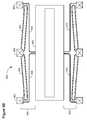
- FIG. 10is a plan view of a four-spring shutter assembly according to an illustrative embodiment of the invention.
- FIG. 11is a trimetric view of an illustrative embodiment of the drive beam anchor and compliant beam anchor structures.
- FIGS. 12A-12Frepresent plan views of illustrative embodiments of the anchor structure elements.
- FIGS. 13A-Crepresent trimetric views of illustrative embodiments of the anchor structure elements.
- FIGS. 14A-Drepresent trimetric views of additional illustrative embodiments of the anchor structure elements.
- FIG. 15is a trimetric view of an illustrative embodiment of a compliant load beam anchor.
- FIG. 16is a trimetric view of an illustrative embodiment of an example two-spring shutter.
- FIG. 17is a trimetric view of an illustrative embodiment of the anchor structure for the drive beam of an example two-spring shutter.
- FIGS. 18A-Brepresent close-up trimetric views of illustrative embodiments of the anchor structure elements.
- FIG. 1is a schematic diagram of a direct-view MEMS-based display apparatus 100 , according to an illustrative embodiment of the invention.
- the display apparatus 100includes a plurality of light modulators 102 a - 102 d (generally “light modulators 102 ”) arranged in rows and columns.
- light modulators 102 a and 102 dare in the open state, allowing light to pass.
- Light modulators 102 b and 102 care in the closed state, obstructing the passage of light.
- the display apparatus 100can be utilized to form an image 104 for a backlit display, if illuminated by a lamp or lamps 105 .
- the apparatus 100may form an image by reflection of ambient light originating from the front of the apparatus.
- the apparatus 100may form an image by reflection of light from a lamp or lamps positioned in the front of the display, i.e. by use of a front light.
- the light modulators 102interfere with light in an optical path by, for example, and without limitation, blocking, reflecting, absorbing, filtering, polarizing, diffracting, or otherwise altering a property or path of the light.
- each light modulator 102corresponds to a pixel 106 in the image 104 .
- the display apparatus 100may utilize a plurality of light modulators to form a pixel 106 in the image 104 .
- the display apparatus 100may include three color-specific light modulators 102 . By selectively opening one or more of the color-specific light modulators 102 corresponding to a particular pixel 106 , the display apparatus 100 can generate a color pixel 106 in the image 104 .
- the display apparatus 100includes two or more light modulators 102 per pixel 106 to provide grayscale in an image 104 .
- a “pixel”corresponds to the smallest picture element defined by the resolution of the image.
- the term “pixel”refers to the combined mechanical and electrical components utilized to modulate the light that forms a single pixel of the image.
- Display apparatus 100is a direct-view display in that it does not require imaging optics. The user sees an image by looking directly at the display apparatus 100 .
- the display apparatus 100is incorporated into a projection display.
- the displayforms an image by projecting light onto a screen or onto a wall.
- the display apparatus 100is substantially smaller than the projected image 104 .
- Direct-view displaysmay operate in either a transmissive or reflective mode.
- the light modulatorsfilter or selectively block light which originates from a lamp or lamps positioned behind the display. The light from the lamps is optionally injected into a light guide or “backlight”.
- Transmissive direct-view display embodimentsare often built onto transparent or glass substrates to facilitate a sandwich assembly arrangement where one substrate, containing the light modulators, is positioned directly on top of the backlight.
- a color specific light modulatoris created by associating a color filter material with each modulator 102 .
- colorscan be generated, as described below, using a field sequential color method by alternating illumination of lamps with different primary colors.
- Each light modulator 102includes a shutter 108 and an aperture 109 .
- the shutter 108is positioned such that it allows light to pass through the aperture 109 towards a viewer.
- the shutter 108is positioned such that it obstructs the passage of light through the aperture 109 .
- the aperture 109is defined by an opening patterned through a reflective or light absorbing material.
- the display apparatusalso includes a control matrix connected to the substrate and to the light modulators for controlling the movement of the shutters.
- the control matrixincludes a series of electrical interconnects (e.g., interconnects 110 , 112 , and 114 ), including at least one write-enable interconnect 110 (also referred to as a “scan-line interconnect”) per row of pixels, one data interconnect 112 for each column of pixels, and one common interconnect 114 providing a common voltage to all pixels, or at least to pixels from both multiple columns and multiples rows in the display apparatus 100 .
- V wethe write-enable interconnect 110 for a given row of pixels prepares the pixels in the row to accept new shutter movement instructions.
- the data interconnects 112communicate the new movement instructions in the form of data voltage pulses.
- the data voltage pulses applied to the data interconnects 112directly contribute to an electrostatic movement of the shutters.
- the data voltage pulsescontrol switches, e.g., transistors or other non-linear circuit elements that control the application of separate actuation voltages, which are typically higher in magnitude than the data voltages, to the light modulators 102 .
- the application of these actuation voltagesthen results in the electrostatic driven movement of the shutters 108 .
- FIG. 2is a perspective view of an illustrative shutter-based light modulator 200 suitable for incorporation into the MEMS-based display apparatus 100 of FIG. 1 , according to an illustrative embodiment of the invention.
- the shutter-based light modulator 200(also referred to as shutter assembly 200 ) includes a shutter 202 coupled to an actuator 204 .
- the actuator 204is formed from two separate compliant electrode beam actuators 205 (the “actuators 205 ”), as described in Hagood et al (U.S. Pat. No. 7,271,945, incorporated herein by reference in its entirety).
- the shutter 202couples on one side to the actuators 205 .
- the actuators 205move the shutter 202 transversely over a surface 203 in a plane of motion which is substantially parallel to the surface 203 .
- the opposite side of the shutter 202couples to a spring 207 which provides a restoring force opposing the forces exerted by the actuator 204 .
- Each actuator 205includes a compliant load beam 206 connecting the shutter 202 to a load anchor 208 .
- the load anchors 208along with the compliant load beams 206 serve as mechanical supports, keeping the shutter 202 suspended proximate to the surface 203 .
- the load anchors 208physically connect the compliant load beams 206 and the shutter 202 to the surface 203 and electrically connect the load beams 206 to a bias voltage, in some instances, ground.
- Each actuator 205also includes a compliant drive beam 216 positioned adjacent to each load beam 206 .
- the drive beams 216couple at one end to a drive beam anchor 218 shared between the drive beams 216 .
- the other end of each drive beam 216is free to move.
- Each drive beam 216is curved such that it is closest to the load beam 206 near the free end of the drive beam 216 and the anchored end of the load beam 206 .
- the surface 203includes one or more apertures 211 for admitting the passage of light. If the shutter assembly 200 is formed on an opaque substrate, made for example from silicon, then the surface 203 is a surface of the substrate, and the apertures 211 are formed by etching an array of holes through the substrate. If the shutter assembly 200 is formed on a transparent substrate, made for example of glass or plastic, then the surface 203 is a surface of a light blocking layer deposited on the substrate, and the apertures are formed by etching the surface 203 into an array of holes 211 .
- the apertures 211can be generally circular, elliptical, polygonal, serpentine, or irregular in shape.
- a display apparatus incorporating the light modulator 200applies an electric potential to the drive beams 216 via the drive beam anchor 218 .
- a second electric potentialmay be applied to the load beams 206 .
- the resulting potential difference between the drive beams 216 and the load beams 206pulls the free ends of the drive beams 216 towards the anchored ends of the load beams 206 , and pulls the shutter ends of the load beams 206 toward the anchored ends of the drive beams 216 , thereby driving the shutter 202 transversely towards the drive anchor 218 .
- the compliant members 206act as springs, such that when the voltage across the beams 206 and 216 is removed, the load beams 206 push the shutter 202 back into its initial position, releasing the stress stored in the load beams 206 .
- the shutter assembly 200also referred to as an elastic shutter assembly, incorporates a passive restoring force, such as a spring, for returning a shutter to its rest or relaxed position after voltages have been removed.
- a passive restoring forcesuch as a spring
- a number of elastic restore mechanisms and various electrostatic couplingscan be designed into or in conjunction with electrostatic actuators, the compliant beams illustrated in shutter assembly 200 being just one example.
- Other examplesare described in Hagood et al (U.S. Pat. No. 7,271,945), and U.S. patent application Ser. No. 11/326,696, both incorporated herein by reference in their entirety. For instance, a highly non-linear voltage-displacement response can be provided which favors an abrupt transition between “open” vs.
- the actuator 205 within the elastic shutter assemblyis said to operate between a closed or actuated position and a relaxed position.
- the designercan choose to place apertures 211 such that shutter assembly 200 is in either the “open” state, i.e. passing light, or in the “closed” state, i.e. blocking light, whenever actuator 205 is in its relaxed position.
- the open statei.e. passing light
- the closed statei.e. blocking light
- control matrix 300is fabricated as a diffused or thin-film-deposited electrical circuit on the surface of a substrate 304 on which the shutter assemblies 302 are formed.
- the control matrix 300includes a scan-line interconnect 306 for each row of pixels 301 in the control matrix 300 and a data-interconnect 308 for each column of pixels 301 in the control matrix 300 .
- Each scan-line interconnect 306electrically connects a write enabling voltage source 307 to the pixels 301 in a corresponding row of pixels 301 .
- Each data interconnect 308electrically connects a data voltage source, (“V d source”) 309 to the pixels 301 in a corresponding column of pixels 301 .
- V d sourcedata voltage source
- the data voltage V dprovides the majority of the energy necessary for actuation of the shutter assemblies 302 .
- the data voltage source 309also serves as an actuation voltage source.
- the control matrix 300includes a transistor 310 and a capacitor 312 .
- the gate of each transistor 310is electrically connected to the scan-line interconnect 306 of the row in the array 320 in which the pixel 301 is located.
- the source of each transistor 310is electrically connected to its corresponding data interconnect 308 .
- the actuators 303 of each shutter assembly 302include two electrodes.
- the drain of each transistor 310is electrically connected in parallel to one electrode of the corresponding capacitor 312 and to one of the electrodes of the corresponding actuator 303 .
- the other electrode of the capacitor 312 and the other electrode of the actuator 303 in shutter assembly 302are connected to a common or ground potential.
- the transistors 310can be replaced with semiconductor diodes and or metal-insulator-metal sandwich type switching elements.
- the control matrix 300write-enables each row in the array 320 in a sequence by applying V we to each scan-line interconnect 306 in turn.
- V weFor a write-enabled row, the application of V we to the gates of the transistors 310 of the pixels 301 in the row allows the flow of current through the data interconnects 308 through the transistors 310 to apply a potential to the actuator 303 of the shutter assembly 302 . While the row is write-enabled, data voltages V d are selectively applied to the data interconnects 308 .
- the data voltage applied to each data interconnect 308is varied in relation to the desired brightness of the pixel 301 located at the intersection of the write-enabled scan-line interconnect 306 and the data interconnect 308 .
- the data voltageis selected to be either a relatively low magnitude voltage (i.e., a voltage near ground) or to meet or exceed Vat (the actuation threshold voltage).
- Vatthe actuation threshold voltage
- the voltage applied to the data interconnect 308remains stored in the capacitor 312 of the pixel 301 even after the control matrix 300 ceases to apply V we to a row. It is not necessary, therefore, to wait and hold the voltage V we on a row for times long enough for the shutter assembly 302 to actuate; such actuation can proceed after the write-enabling voltage has been removed from the row.
- the capacitors 312also function as memory elements within the array 320 , storing actuation instructions for periods as long as is necessary for the illumination of an image frame.
- the pixels 301 as well as the control matrix 300 of the array 320are formed on a substrate 304 .
- the arrayincludes an aperture layer 322 , disposed on the substrate 304 , which includes a set of apertures 324 for respective pixels 301 in the array 320 .
- the apertures 324are aligned with the shutter assemblies 302 in each pixel.
- the substrate 304is made of a transparent material, such as glass or plastic.
- the substrate 304is made of an opaque material, but in which holes are etched to form the apertures 324 .
- Control matrix 300Components of shutter assemblies 302 are processed either at the same time as the control matrix 300 or in subsequent processing steps on the same substrate.
- the electrical components in control matrix 300are fabricated using many thin film techniques in common with the manufacture of thin film transistor arrays for liquid crystal displays. Available techniques are described in Den Boer, Active Matrix Liquid Crystal Displays (Elsevier, Amsterdam, 2005), incorporated herein by reference.
- the shutter assembliesare fabricated using techniques similar to the art of micromachining or from the manufacture of micromechanical (i.e., MEMS) devices. Many applicable thin film MEMS techniques are described in Rai-Choudhury, ed., Handbook of Microlithography, Micromachining & Microfabrication (SPIE Optical Engineering Press, Bellingham, Wash. 1997), incorporated herein by reference.
- the shutter assembly 302can be formed from thin films of amorphous silicon, deposited by a chemical vapor deposition process.
- the shutter assembly 302 together with the actuator 303can be made bi-stable. That is, the shutters can exist in at least two equilibrium positions (e.g. open or closed) with little or no power required to hold them in either position. More particularly, the shutter assembly 302 can be mechanically bi-stable. Once the shutter of the shutter assembly 302 is set in position, no electrical energy or holding voltage is required to maintain that position. The mechanical stresses on the physical elements of the shutter assembly 302 can hold the shutter in place.
- the shutter assembly 302 together with the actuator 303can also be made electrically bi-stable.
- an electrically bi-stable shutter assemblythere exists a range of voltages below the actuation voltage of the shutter assembly, which if applied to a closed actuator (with the shutter being either open or closed), holds the actuator closed and the shutter in position, even if an opposing force is exerted on the shutter.
- the opposing forcemay be exerted by a spring such as spring 207 in shutter-based light modulator 200 , or the opposing force may be exerted by an opposing actuator, such as an “open” or “closed” actuator.
- the light modulator array 320is depicted as having a single MEMS light modulator per pixel. Other embodiments are possible in which multiple MEMS light modulators are provided in each pixel, thereby providing the possibility of more than just binary “on” or “off” optical states in each pixel. Certain forms of coded area division gray scale are possible where multiple MEMS light modulators in the pixel are provided, and where apertures 324 , which are associated with each of the light modulators, have unequal areas.
- roller-based light modulator 220 and the light tap 250can be substituted for the shutter assembly 302 within the light modulator array 320 .
- FIGS. 4A and 4Billustrate an alternative shutter-based light modulator (shutter assembly) 400 suitable for inclusion in various embodiments of the invention. Because four actuators accomplish the task of moving the shutter (two per side, making up actuators 402 and 404 ), this arrangement is referred to as a four-spring shutter.
- the light modulator 400is an example of a dual actuator shutter assembly, and is shown in FIG. 4A in an open state.
- FIG. 4Bis a view of the dual actuator shutter assembly 400 in a closed state.
- Shutter assembly 400is described in further detail in Hagood et al (U.S. Pat. No. 7,271,945) incorporated herein by reference in its entirety.
- shutter assembly 400includes actuators 402 and 404 on either side of a shutter 406 .
- Each actuator 402 and 404is independently controlled.
- a first actuator, a shutter-open actuator 402serves to open the shutter 406 .
- a second opposing actuator, the shutter close actuator 404serves to close the shutter 406 .
- Both actuators 402 and 404are compliant beam electrode actuators.
- the actuators 402 and 404open and close the shutter 406 by driving the shutter 406 substantially in a plane parallel to an aperture layer 407 over which the shutter is suspended.
- the shutter 406is suspended a short distance over the aperture layer 407 by anchors 408 attached to the actuators 402 and 404 .
- the inclusion of supports attached to both ends of the shutter 406 along its axis of movementreduces out of plane motion of the shutter 406 and confines the motion substantially to a plane parallel to the substrate.
- the shutter 406includes two shutter apertures 412 through which light can pass.
- the aperture layer 407includes a set of three apertures 409 .
- FIG. 4Athe shutter assembly 400 is in the open state and, as such, the shutter-open actuator 402 has been actuated, the shutter-close actuator 404 is in its relaxed position, and the centerlines of apertures 412 and 409 coincide.
- FIG. 4Bthe shutter assembly 400 has been moved to the closed state and, as such, the shutter-open actuator 402 is in its relaxed position, the shutter-close actuator 404 has been actuated, and the light blocking portions of shutter 406 are now in position to block transmission of light through the apertures 409 (shown as dotted lines).
- Each aperturehas at least one edge around its periphery.
- the rectangular apertures 409have four edges.
- each aperturemay have only a single edge.
- the aperturesneed not be separated or disjoint in the mathematical sense, but instead can be connected. That is to say, while portions or shaped sections of the aperture may maintain a correspondence to each shutter, several of these sections may be connected such that a single continuous perimeter of the aperture is shared by multiple shutters.
- FIG. 4Bshows a predefined overlap 416 between the edge of light blocking portions in the shutter 406 and one edge of the aperture 409 formed in aperture layer 407 .
- the electrostatic actuators 402 and 404are designed so that their voltage displacement behavior provides a bi-stable characteristic to the shutter assembly 400 .
- the minimum voltage needed to maintain a shutter's position against such an opposing forceis referred to as a maintenance voltage V m .
- a number of control matriceswhich take advantage of the bistable operation characteristic are described in U.S. patent application Ser. No. 11/607,715, referenced above.
- FIG. 5is a plan view of an illustrative embodiment of a light modulation assembly.
- a two-spring shutter assembly 500(so called “two-spring” because there is one load beam ( 502 , 503 ) each attached to a shutter end (where the shutter end represents either the top or the bottom of the shutter), unlike the “four-spring” shutter assembly 400 , where there are two load beams per shutter end.
- each load beam ( 502 , 503 )is connected at one end to the shutter 504 and at the other to an anchor structure ( 508 for beam 502 and 506 for beam 503 ).
- the shelves within the anchor structurescreate a reference plane above the substrate to which the load beams are attached.
- This elevation and connection to the shutter through the load beams ( 502 , 503 )help to suspend the shutter 504 a specified distance above the surface.
- these attachment points ( 510 , 512 )are on opposite sides of the shutter 504 .
- This embodimenthas demonstrated advantages in keeping the shutter from rotating around the axis normal to the substrate surface upon actuation.
- the load beamsare connected to the other corners of the shutter.
- the drive beams ( 526 , 528 )are similarly suspended above the surface of the substrate by their anchor structures ( 522 , 524 ).
- the shuttermoves from one position to another by the electric attraction of its load beams ( 502 , 503 ) to their respective drive beams ( 526 , 528 ).
- To move the shutter 504 towards drive beam 526we set the potential of drive beam 526 to a different value than the potential of shutter 504 , while keeping drive beam 528 the same potential as shutter 504 .
- drive beamsare cantilevered beams that are each attached to a respective anchor ( 522 , 524 ). More is discussed about these in FIGS. 8A and 8B .
- the shutter 504is disposed on a transparent substrate preferably made of glass or plastic.
- a rear-facing reflective layer disposed on the substrate below the shutterdefines a plurality of surface apertures located beneath the shutter.
- the vertical gap that separates the shutter from the underlying substrateis in the range of 0.1 to 10 microns.
- the magnitude of the vertical gapis preferably less than the lateral overlap between the edge of shutter and the edge of aperture in the closed state, such as the overlap 416 shown in FIG. 4B .
- FIG. 6Ashows cross sectional detail of a composite shutter assembly 600 , including shutter 601 , a compliant beam 602 , and anchor structure 604 built-up on substrate 603 and aperture layer 606 according to one implementation of the MEMS-based shutter display.
- the elements of the composite shutter assemblyinclude a first mechanical layer 605 , a conductor layer 607 , a second mechanical layer 609 , and an encapsulating dielectric 611 . At least one of the mechanical layers 605 or 609 will be deposited to thicknesses in excess of 0.15 microns, as one or both of the mechanical layers will comprise the principle load bearing and mechanical actuation member for the shutter assembly.
- Candidate materials for the mechanical layers 605 and 609include, without limitation, metals such as AI, Cu, Ni, Cr, Mo, Ti, Ta, Nb, Nd, or alloys thereof; dielectric materials such as Al 2 O 3 , TiO 2 , Ta 2 O 5 , or Si 3 N 4 ; or semiconducting materials such as diamond-like carbon, Si, Ge, GaAs, CdTe or alloys thereof. At least one of the layers, such as conductor layer 607 , should be electrically conducting so as to carry charge on to and off of the actuation elements.
- FIG. 6Ashows a sandwich configuration for the composite in which the mechanical layers 605 and 609 with similar thicknesses and mechanical properties are deposited on either side of the conductor layer 607 .
- the sandwich structurehelps to ensure that stresses remaining after deposition and/or stresses that are imposed by temperature variations will not act cause bending or warping of the shutter assembly 600 .
- the order of the layers in composite shutter assembly 600can be inverted, such that the outside of the sandwich is comprised of a conducting layer while the inside of the sandwich is comprised of a mechanical layer.
- Shutter assembly 600includes an encapsulating dielectric layer 611 .
- Dielectric coatingscan be applied in conformal fashion, such that all bottom, tops, and side surfaces of the shutters and beams are uniformly coated. Such thin films can be grown by thermal oxidation and/or by conformal chemical vapor deposition of an insulator such as Al 2 O 3 , Cr 2 O 3 , TiO 2 , HfO 2 , V 2 O 5 , Nb 2 O 5 , Ta 2 O 5 , SiO 2 , or Si 3 N 4 , or by depositing similar materials by means of atomic layer deposition.
- the dielectric coating layercan be applied with thicknesses in the range of 5 nm to 1 micron. In some cases sputtering and evaporation can be used to deposit the dielectric coating onto sidewalls.
- FIGS. 6B-6Eshow the process for building shutter assembly 600 , including shutter 601 , a compliant beam 602 , and anchor structure 604 on top of a substrate 603 and aperture layer 606 .
- the shutter assemblyis built on top of a pre-existing control matrix, for instance an active matrix array of thin film transistors.
- the processes used for constructing the control matrix on top of or in conjunction with an aperture layer 606is described in Brosnihan (U.S. Pat. No. 7,405,852) referred to and incorporated above.
- FIG. 6Bis a cross sectional view of a first step in the process of forming the shutter assembly 600 according to an illustrative embodiment of the invention.
- a sacrificial layer 613is deposited and patterned.
- Polyimideis a preferred sacrificial material.
- Other candidate sacrificial materialsinclude polymer materials such as polyamide, fluoropo lymer, benzocyclobutene, polyphenyl quinoxylene, parylene, or polynorbornene. These materials are chosen for their ability to planarize rough surfaces, maintain mechanical integrity at processing temperatures in excess of 250 C, and their ease of etch and/or thermal decomposition during removal.
- Alternate sacrificial layerscan be found among the photoresists: polyvinyl acetate, polyvinyl ethylene, and phenolic or novolac resins, although their use will typically be limited to temperatures below 350 C.
- An alternate sacrificial layeris SiO 2 , which can be removed preferentially as long as other electronic or structural layers are resistant to the hydrofluoric acid solutions used for its removal (Si 3 N 4 is so resistant).
- Another alternate sacrificial layeris silicon, which can be removed preferentially as long as other electronic and structural layers are resistant to the fluorine plasmas or XeF 2 used for its removal (most metals and/or Si 3 N 4 are so resistant).
- Yet another alternate sacrificial layeris aluminum, which can be removed preferentially as long as other electronic or structural layers are resistant to strong base (concentrated NaOH) solutions (Cr, Ni, Mo, Ta, and Si are so resistant). Still another alternate sacrificial layer is copper, which can be removed preferentially as long as other electronic or structural layers are resistant to nitric or sulfuric acid solutions (Cr, Ni, and Si are so resistant).
- the sacrificial layer 613is patterned to expose holes or vias at the anchor regions 604 .
- the preferred polyimide material and other polymer resinscan be formulated to include photoactive agents—enabling regions exposed through a UV photomask to be preferentially removed in a developer solution.
- Other sacrificial layers 613can be patterned by coating the sacrificial layer in an additional layer of photoresist, photopatterning the photoresist, and finally using the photoresist as an etching mask.
- Other sacrificial layerscan be patterned by coating the sacrificial layer with a hard mask, which can be a thin layer of SiO 2 or metal such as chromium.
- a photopatternis then transferred to the hard mask by means of photoresist and wet chemical etching.
- the pattern developed in the hard maskcan be very resistant to dry chemical, anisotropic, or plasma etching—techniques which can be used to impart very deep and narrow anchor holes into the sacrificial layer.
- the exposed and underlying conducting surface 614can be etched, either chemically or via the sputtering effects of a plasma, to remove any surface oxide layers.
- Such a contact etching stepcan improve the ohmic contact between the underlying conductor and the shutter material.
- any photoresist layers or hard maskscan be removed through use of either solvent cleans or acid etching.
- the shutter assembly 600is composed of multiple thin films 605 , 607 , and 609 .
- the first mechanical layer 605is an amorphous silicon layer, deposited first, followed by a conductor layer 607 comprised of aluminum, followed by a second layer 609 of amorphous silicon.
- the deposition temperature used for the shutter materials 605 , 607 , and 609is below that at which physical degradation occurs for the sacrificial layer. For instance, polyimide is known to decompose at temperatures above 400 C.
- the shutter materials 605 , 607 and 609can be deposited at temperatures below 400 C, thus allowing usage of polyimide as a sacrificial material.
- Hydrogenated amorphous siliconis a useful mechanical material for layers 605 and 609 since it can be grown to thicknesses in the range of 0.1 to 3 microns, in a relatively stress-free state, by means of plasma-assisted chemical vapor deposition (PECVD) from silane gas at temperatures in the range of 250 to 350 C.
- PECVDplasma-assisted chemical vapor deposition
- Phosphene gas (PH 3 )is used as a dopant so that the amorphous silicon can be grown with resistivities below 1 ohm-cm.
- a similar PECVD techniquecan be used for the deposition of Si 3 N 4 , silicon-rich Si 3 N 4 , or SiO 2 materials as the mechanical layer 605 or for the deposition of diamond-like carbon, Ge, SiGe, CdTe, or other semiconducting materials for mechanical layer oxynitride 605 .
- An advantage of the PECVD deposition techniqueis that the deposition can be quite conformal, that is, it can coat a variety of inclined surfaces or the inside surfaces of narrow via holes. Even if the anchor or via holes which are cut into the sacrificial material present nearly vertical sidewalls, the PECVD technique can provide a continuous coating between the bottom and top horizontal surfaces of the anchor.
- shutter layers 605 or 609include RF or DC sputtering, metal-organic chemical vapor deposition, evaporation, electroplating or electroless plating.
- a metal thin filmsuch as Al is preferred, although alternates such as Cu, Ni, Mo, or Ta can be chosen.
- the inclusion of such a conducting materialserves two purposes. It reduces the overall sheet resistance of the shutter material and it helps to block the passage of visible light through the shutter material. (Amorphous silicon can be doped to be conductive, however, if grown to thicknesses of less than 2 microns can transmit visible light to some degree.)
- the conducting materialcan be deposited either by sputtering or, in a more conformal fashion, by chemical vapor deposition techniques, electroplating, or electroless plating.
- the process for building the shutter assembly 600continues in FIG. 6D .
- the shutter layers 605 , 607 , and 609are photomasked and etched while the sacrificial layer 613 is still on the wafer.
- Amorphous silicon, silicon nitride, and silicon oxidecan then be etched in fluorine-based plasma chemistries.
- SiO 2 mechanical layerscan be etched using HF wet chemicals; and any metals in the conductor layers can be etched with either wet chemicals or chlorine-based plasma chemistries.
- the pattern shapes applied through the photomask at FIG. 6Dinfluence the mechanical properties, such as stiffness, compliance, and the voltage response in the actuators and shutters of the shutter assembly 600 .
- the shutter assembly 600includes a compliant beam 602 , shown in cross section. Compliant beam 602 is shaped such that the width is less than the total height or thickness of the shutter material. It is preferable to maintain a beam dimensional ratio of at least 1.4:1, with the beams 602 being taller or thicker than they are wide.
- the process for building the shutter assembly 600continues as depicted in FIG. 6E .
- the sacrificial layer 613is removed, which frees-up all moving parts from the substrate 603 , except at the anchor points.
- Polyimide sacrificial materialsare preferably removed in an oxygen plasma.
- Other polymer materials used for sacrificial layer 613can also be removed in an oxygen plasma, or in some cases by thermal pyrolysis.
- Some sacrificial layers 613(such as SiO 2 ) can be removed by wet chemical etching or by vapor phase etching.
- a dielectric coating 611is deposited on all exposed surfaces of the shutter.
- Dielectric coatings 611can be applied in conformal fashion, such that all bottom, tops, and side surfaces of the shutters 601 and beams 602 are uniformly coated using chemical vapor deposition.
- Al 2 O 3is a preferred dielectric coating for layer 611 , which is deposited by atomic layer deposition to thicknesses in the range of 10 to 100 nanometers.
- anti-stiction coatingscan be applied to the surfaces of all shutters 601 and beams 602 . These coatings prevent the unwanted stickiness or adhesion between two independent beams of an actuator.
- Applicable coatingsinclude carbon films (both graphite and diamond-like) as well as fluoropolymers, and/or low vapor pressure lubricants. These coatings can be applied by either exposure to a molecular vapor or by decomposition of a precursor compounds by means of chemical vapor deposition.
- Anti-stiction coatingscan also be created by the chemical alteration of shutter surfaces, as in the fluoridation, silanization, siloxidation, or hydrogenation of insulating surfaces.
- U.S. Pat. No. 7,271,945incorporated herein by reference in its entirety, describes a number of useful designs for shutter assemblies and actuators.
- One class of suitable actuators for use in MEMS-based shutter displaysinclude compliant actuator beams for controlling shutter motion that is transverse to or in-the-plane of the display substrate. The voltage necessary for the actuation of such shutter assemblies decreases as the actuator beams become more compliant. The control of actuated motion also improves if the beams are shaped such that in-plane motion is preferred or promoted with respect to out-of-plane motion.
- the compliant actuator beamshave a rectangular cross section, such as beam 602 of FIG. 6A , such that the beams are taller or thicker than they are wide.
- the stiffness of a long rectangular beam with respect to bending within a particular planescales with the thinnest dimension of that beam in that plane to the third power. It is of interest, therefore, to reduce the width of the compliant beams as far as possible to reduce the actuation voltages for in-plane motion.
- the minimum width of the beamsis usually limited to the resolution of the exposure optics.
- photolithography equipmenthas been developed for defining patterns in photoresist with features as narrow as 15 nanometers, such equipment is expensive and the areas over which patterning can be accomplished in a single exposure are limited.
- the patterning resolution or minimum feature sizeis typically limited to 1 micron or 2 microns or greater.
- FIGS. 7A through 7Ddescribe a technique, illustrated in FIGS. 7A through 7D , whereby a shutter assembly 700 with compliant actuator beams 716 can be fabricated at dimensions well below the conventional lithography limits on large glass panels.
- the compliant beams of shutter assembly 700are formed as sidewall features on a mold made from a sacrificial material. The process is referred to as a sidewall beams process.
- the process of forming a shutter assembly 700 with sidewall beamsbegins, as shown in FIG. 7A , with the deposition and patterning of a first sacrificial material 701 .
- the pattern defined in the first sacrificial materialcreates openings or vias 702 within which anchors for the shutter will eventually be formed.
- the deposition and patterning of the first sacrificial material 701is similar in concept, and uses similar materials, as those described for the deposition and patterning described in relation to FIGS. 6A-6E .
- FIG. 7Bshows the shape of a mold 703 that is created after patterning of the second sacrificial material 705 .
- the mold 703also includes the first sacrificial material 701 with its previously defined vias 702 .
- the mold 703 in FIG. 7Bincludes two distinct horizontal levels: The bottom horizontal level 708 of mold 703 is established by the top surface of the first sacrificial layer 701 and is accessible in those areas where the second sacrificial layer 705 has been etched away.
- the top horizontal level 710 of the mold 703is established by the top surface of the second sacrificial layer 705 .
- the mold 703 illustrated in FIG. 7Balso includes substantially vertical sidewalls 709 .
- the process of forming sidewall beamscontinues with the deposition and patterning of the shutter material onto all of the exposed surfaces of the sacrificial mold 703 , as depicted in FIG. 7C .
- the preferred materials for use in shutter 712are described above with respect to the shutter materials 605 , 607 , and 609 . Alternate shutter materials and/or shutter coatings are described in Brosnihan (U.S. Pat. No. 7,405,852).
- the shutter materialis deposited to a thickness of less than about 2 microns. In some implementations, the shutter material is deposited to have a thickness of less than about 1.5 microns.
- the shutter materis deposited to have a thickness of less than about 1.0 microns, and as thin as about 0.10 microns.
- the shutter material(which may be a composite shutter as described above) is patterned, as shown in FIG. 7C .
- the pattern developed into the photoresistis designed such that shutter material remains in the region of shutter 712 as well as at the anchors 714 .
- anisotropic etchof the shutter material is carried out in a plasma atmosphere with a voltage bias applied to the substrate, or to an electrode in proximity to the substrate.
- the biased substrate(with electric field perpendicular to the surface of the substrate) leads to acceleration of ions toward the substrate at an angle nearly perpendicular to the substrate.
- Such accelerated ionscoupled with the etching chemicals, lead to etch rates that are much faster in a direction that is normal to the plane of the substrate as compared to directions parallel to the substrate. Undercut-etching of shutter material in the regions protected by photoresist is thereby substantially eliminated.
- the shutter materialis also substantially protected from the anisotropic etch. Such protected sidewall shutter material will later form compliant beams 716 for supporting the shutter 712 .
- the shutter materialhas been completely removed by the etch.
- the anisotropic etch used to form sidewall beams 716can be achieved in either an RF or DC plasma etching device as long as provision for electrical bias of the substrate, or of an electrode in close proximity of the substrate, is supplied.
- an equivalent self-biascan be obtained by disconnecting the substrate holder from the grounding plates of the excitation circuit, thereby allowing the substrate potential to float in the plasma.
- an etching gassuch as CHF3, C4F8, or CHCl 3 in which both carbon and hydrogen and/or carbon and fluorine are constituents in the etch gas.
- the liberated C, H, and/or F atomscan migrate to the sidewalls 709 where they build up a passive or protective quasipolymer coating.
- This quasi-polymer coatingfurther protects the sidewall beams 716 from etching or chemical attack.
- the process of forming sidewall beamsis completed with the removal of the remainder of the second sacrificial layer 705 and the first sacrificial layer 701 , the result being shown in FIG. 7D .
- the process of removing sacrificial materialis similar to that described with respect to FIG. 6E .
- the material deposited on the sidewalls 709 of the mold 703remain as the compliant beams 716 .
- the compliant beams 716mechanically connect the anchors 714 to the shutter 712 .
- the anchorsconnect to an aperture layer 725 .
- the compliant beams 716are tall and narrow.
- the width of the sidewall beams 716as formed from the surface of the mold 703 , is similar to the thickness of the shutter material as deposited.
- the beam width at 716will be the same as the thickness of the horizontal shutter material at 712 , in other cases the beam width will be only about 1 ⁇ 2 the thickness of the shutter material.
- the height of the sidewall beams 716is determined by the thickness of the second sacrificial material 705 , or in other words, by the depth of the mold 703 as created during the patterning step described in relation to FIG. 7B .
- the thickness of the deposited shutter materialis chosen to be less than 2 microns (for many applications the thickness range of 0.1 to 2.0 micron is suitable)
- the method illustrated in FIGS. 7A-7Dis well suited for the production of very narrow beams.
- Conventional photolithographywould limit the patterned features shown in FIGS. 7A , 7 B, and 7 C to much larger dimensions, for instance allowing minimum resolved features no smaller than 2 microns or 5 microns.
- FIG. 7Ddepicts an isometric view of a shutter assembly 700 , formed after the release step in the above-described process, yielding compliant beams with cross sections of high aspect ratio.
- the thickness of the second sacrificial layeris, for example, greater than 4 times larger than the thickness of the shutter material, the resulting ratio of beam height to beam width will be produced to a similar ratio, i.e. greater than 4.
- An optional stepinvolves isotropic etching of sidewall beams 716 to separate or decouple beams formed along the sidewalls of mold 703 .
- the shutter material at point 724has been removed from the sidewall through use of an in isotropic etch.
- An isotropic etchis one whose etch rate is the same in all directions, so that sidewall material in regions such as point 724 is no longer protected.
- the isotropic etchcan be accomplished in the typical plasma etch equipment as long as a bias voltage is not applied to the substrate. Isotropic etch can also be achieved using wet chemical or vapor phase etching techniques.
- the separation of beams at point 724is achieved through a distinct sequence of photoresist dispense, patterning, and etch.
- the photoresist pattern in this caseis designed to protect the sidewall beams 716 from the isotropic etch chemistry but expose the sidewall beams at point 724 .
- an encapsulating dielectricsuch as dielectric 611 is deposited around the outside surfaces of the sidewall beams.
- the sidewalls 709can be made as vertical as possible. Slopes at the sidewalls 709 and/or exposed surfaces become susceptible to the anisotropic etch. Vertical sidewalls 709 can be produced if the patterning step at FIG. 7B , the patterning of the second sacrificial material 705 , is also carried out in anisotropic fashion.
- the surfaces of the mold 703are preferably covered with similar thicknesses of shutter material, regardless or the orientation of those surfaces, either vertical or horizontal.
- Such conformalitycan be achieved when depositing with a chemical vapor deposition technique (CVD).
- CVDchemical vapor deposition technique
- the following conformal techniquescan be employed: plasma enhanced chemical vapor deposition (PECVD), low pressure chemical vapor deposition (LPCVD), and atomic or self-limited layer deposition (ALD).
- PECVDplasma enhanced chemical vapor deposition
- LPCVDlow pressure chemical vapor deposition
- ALDatomic or self-limited layer deposition
- the growth rate of the thin filmcan be limited by reaction rates on a surface as opposed to exposing the surface to a directional flux of source atoms.
- the thickness of material grown on vertical surfacesis preferably at least 50% of the thickness of material grown on horizontal surfaces.
- shutter materialscan be conformally deposited from solution by electroless plating or electroplated, as long as a metal seed layer is provided that uniformly coats all surfaces before plating.
- the shutter assembly, beams, and anchor structuresare shell structures formed using the MEMS sidewall beams process described above.
- the load-bearing anchoring structureis constructed using two basic elements, a sidewall and a shelf. Both of these surfaces may be totally or partially flat, curved, angled, or multi-faceted, with the distinction that a sidewall is a primarily non-horizontal surface with respect to the plane of the substrate, and a shelf is a surface primarily parallel to the plane of the substrate.
- the sidewall and shelf surfacesare substantially orthogonal to each other, where the angle between such substantially orthogonal surfaces shall not be less than 20 degrees or greater than 160 degrees.
- the anchor structureis formed using a combination of the above-described sidewalls and shelves in order to enhance the second moment of inertia about one or more axes. Also known as the second moment of area, the second moment of inertia of a structure predicts its resistance to bending and is dependent on the geometry of the cross-section of the structure. For example, I-beams have a higher second moment of inertia than other beams of the same cross-sectional area and are the preferred building material because of their resistance to bending. Constructing anchor structures from coupled or interconnected sidewalls and shelves creates structures with a higher second moment of inertia that resists the deflection of beams attached to them. The above effect is better understood when we look at the simplest structural element using this principle.
- the use of a combination of sidewalls and shelves to create a corrugated anchor structurenot only increases the second moment of inertia about one or more axes but also increases the polar moment of inertia about one or more axes and therefore increases the torsional stiffness of the anchor structure. Any increase in the second moment of inertia by changing the anchor structure will also generally result in an increase of the polar moment of inertia of that same anchor structure. In any subsequent references to the enhancement of the second moment of inertia, an enhancement of the polar moment of inertia is also implied, and vice versa.
- FIG. 13Aillustrates a simple anchor structure, constructed from the combination of the sidewalls and shelves described above. These elements can be combined in various embodiments to construct a stiffer anchor structure.
- One of the critical functions of the anchor structureis to secure the shutter assembly to the underlying substrate.
- the substrate surface onto which the anchor is attachedis also referred to as a primary or horizontal surface.
- the part of the anchor structure attached or coupled to the substrate surface and is comprised of one or more sidewallsis the non-horizontal elevating portion (NHEP) 1504 .
- this NHEPis formed by at least one sidewall.
- Other embodimentsmay be formed by the combination of two or more vertically-coupled NHEPs that form a vertical corner rising from the substrate.
- Yet other embodimentsmay be formed out of two or more vertically unconnected (or partially-coupled) NHEPs.
- These non-horizontal elevating portionsalso provide the critical vertical separation of the beams and shutter body from the substrate.
- the substantially horizontal shelf, 1506Coupled to the NHEP is the substantially horizontal shelf, 1506 .
- the substantially-horizontal shelf portionsare all coupled, generating a surface with increased torsional stiffness in all axes.
- the shelf portionsmay be partially coupled or connected.
- the shelfrepresents a substantially-horizontal surface on which to create a non-horizontal, shell-stiffening portion (NHSSP) 1510 to which the beam 1502 is coupled or connected.
- the beam 1502can be connected to NHSSP 1510 at any location other than that connected to the shelf 1506 .
- FIG. 14depicts some of these possible configurations.
- FIGS. 14C-Ddepict embodiments where beam 1502 is a horizontal beam, and it attaches to the upper portion of the NHSSP from the substantially horizontal shelf 1506 .
- FIG. 14Dshows a similar embodiment to FIG. 14C where beam 1502 is also horizontal but in this case the beam attaches to the lower portion of the NHSSP.
- the structure shown in FIG. 13Ahas significant advantages in stiffness and support of any beams coupled to it, especially over the simple coupling of beams to the non-horizontal elevating portions (NHEP).
- NHEPnon-horizontal elevating portions
- non-horizontal portionsbe they elevating portions, NHEP, or shell stiffening portions, NHSSP
- substantially-horizontal shelf sectionshas the effect of creating structural folds, similar to corrugated cardboard construction, such as in FIG. 17 . These structural folds provide additional stiffness to the anchor and also ensure the required elevation for the beams above the substrate.
- FIG. 13Billustrates an example embodiment that further enhances the stiffness of the anchor by adding NHSSP 1512 , which couples to NHSSP 1510 and shelf 1506 .
- the resulting anchor structureincreases the resistance of the beam 1502 to vertical deflection, and also increases the resistance of the beam 1502 to torsion, or rotation along its length axis. This in turn increases the resistance of such a beam to forces that may deflect the beam and resultantly the shutter attached to the beam up or down. Note that many structures would make this possible, including one where the angle of the NHSSP to the shelf is substantially shallow, as long as the NHSSPs are continuously coupled to each other and the shelf.
- FIG. 13Cextends from FIG. 13B by adding NHSSP 1514 , which couples to both NHSSP 1512 and shelf 1506 , and further stiffens the anchor structure.
- FIGS. 13A-Cillustrate the case when the anchor structure is built using near-orthogonal surfaces, it is clear many embodiments are possible utilizing alternate angles. While the most efficient increase in stiffness is generated by maximizing the orthogonality between elements, any continuous change of angle between elements contributes to stiffness. Therefore, though the optimal angle is 90 degrees, the stiffness is affected given any change of angle between NHEP 1512 and NHEP 1510 . Thus, we can see in the illustrative embodiments of FIGS. 12D (round bend), 12 E (semi-circular loop) and 12 F (Triangular bend) that a similar effect to that of FIG. 12A is created.
- FIGS. 12Dround bend
- 12 Esini-circular loop
- 12 FTriangular bend
- FIG. 12Dillustrates an example embodiment (similar to that of FIG. 12B ) where the substantially-orthogonal NHSSPs 1510 and 1512 are implemented as a single, continuous entity.
- two or more unit normal vectors taken from the surface of the non-horizontal shell stiffening portion 1520are substantially different.
- the combined NHSSPs 1510 , 1512 , and 1514 of FIG. 13Care combined into a single, continuous U structure, where again, two or more unit normal vectors taken from the surface of the non-horizontal shell stiffening portion 1522 are substantially different.
- the aboveis the minimum, but significantly enhanced performance may be obtained when more sidewall/shelf combinations are used.
- the above conceptmay be embodied through various shelf/sidewall pairings.
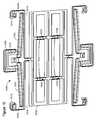
- FIG. 8Aillustrates a portion of a light modulation assembly 802 including dual compliant actuator assemblies 804 and 805 which are functionally similar to the actuators 402 and 404 designed for the shutter assembly 400 according to an illustrative embodiment of the invention.
- a design like thisis referred to as a four-spring design, for each shutter end has two load beams ( 808 , 809 , 820 , 822 ) attached to them.
- the actuators on one sidee.g. the shutter-open actuators, include drive beams ( 806 , 807 ) along with compliant load beams ( 808 , 809 ).
- the load beams ( 808 , 809 )support the shutter 810 at one of its ends, and are attached to respective load beam anchors ( 812 , 813 ) at the other. Both of the drive beams ( 806 , 807 ) are attached to a central drive beam anchor 814 at one end of sais beam and attached to supplementary drive beam anchors ( 816 , 817 ) at the other end of the beam. The arrangement is repeated on the other end of the shutter ( 820 , 822 ). The load beams on the other side of the shutter ( 820 , 822 ) are associated with the shutter-closed actuator 805 .
- the supplementary drive beam anchors ( 816 , 817 )act to limit the deformation or shape change which might otherwise occur within the drive beams ( 806 , 807 ).
- a mechanical beam, such as beam 806which is fixed, supported, or anchored at two points along its length will more easily retain its shape even under the influence of residual stresses or external loads. Note that the drive beam 806 is still free to move or deform at points in between the anchors 814 and 816 and is therefore partially compliant, so that the actuation voltage of the actuator assembly 804 is still less than would be the case with a completely rigid drive beam.
- FIG. 8Billustrates a portion of a shutter assembly 852 including dual compliant actuator assembly 854 , which is functionally similar to the actuator 404 designed for the shutter assembly 400 according to an illustrative embodiment of the invention.
- the actuator assembly 854includes compliant drive beams ( 856 , 857 ) along with compliant load beams ( 858 , 859 ).
- the load beams ( 858 , 859 )support the shutter 860 on one end and are respectively attached to load beam anchors ( 862 , 863 ) at the other end.
- the drive beams ( 856 , 857 )are formed into a loop wherein each end of the drive beam is attached to a common anchor 864 .
- FIG. 9illustrates a portion of a shutter assembly 902 including dual compliant actuator assembly 904 which is functionally similar to the actuator assembly 404 designed for the shutter assembly 400 according to one illustrative embodiment of the invention.
- the actuator assembly 904includes compliant drive beams ( 906 , 907 ) along with compliant load beams ( 908 , 909 ).
- the load beams ( 908 , 909 )support the shutter 910 on one end and are attached to respective load beam anchors ( 912 , 913 ) at the other end.
- Both of the drive beams ( 906 , 907 )are attached to a central drive beam anchor 914 at one end and attached to respective drive beam supplementary anchors ( 916 , 917 ) at the other end.
- the drive beam supplementary anchors ( 916 , 917 )are positioned and the drive beams ( 906 , 907 ) are shaped so as to form a partial loop.
- the drive beams ( 906 , 907 )are shaped so as to form a partial loop.
- the lengths of these two straight line sections in the loopare not equal. This asymmetry provides the opportunity to create or allow for an advantageous shape change in the loop after release from the mold.
- the forces experienced at the distal end of the loopcan cause it be move in a direction parallel to the substrate.
- a small or controlled motion of the distal end of drive beam 906 after release from the mold and in a direction toward the load beams ( 908 , 909 )can thereby be promoted. This motion can be accomplished with a minimum risk that the drive beams ( 906 , 907 ) and the load beams ( 908 , 909 ) will actually touch before the encapsulating dielectric is applied.
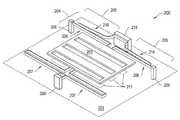
- FIG. 10shows an trimetric projection of light-modulator assembly 1000 including dual-compliant actuators on each end of the shutter 1002 , according to an illustrative embodiment of the invention.
- the actuator assemblyincludes compliant drive beams ( 1004 , 1006 ) along with compliant load beams ( 1008 , 1010 ).
- the load beams ( 1008 , 1010 )support shutter 1002 at one end and are each attached to a load beam anchor ( 1012 , 1014 ) at the other end.
- the drive beams ( 1004 , 1006 )are formed into a loop wherein each end of the drive beam is attached to common anchor 1016 .
- the drive beamsare cantilevered (supported only on one side) to anchor 1016 , and loops ( 1004 L, 1006 L) are free to move.
- the inclusion of a looped shape for drive beams 1004 L and 1006 Lhelps to minimize any in-plane deflection of the drive beams that might result from stresses in the beams.
- the drive beamsare prone to change their elevation above the substrate as a result of its own stresses.
- a change in elevation above the substrate of the shutter load beam ( 1008 , 1010 )could subsequently change the elevation of the shutter.
- the designerprefers to maintain the shutter at a certain fixed elevation above the aperture. If the shutter is too close to the substrate, the result could be the shutter permanently “sticking” to the substrate. Such contact risks the loss of shutter movement, and could result in a potential loss of a pixel in the display. Conversely, if the shutter were elevated above its design elevation, light leakage may increase. This would result in loss of optical contrast at that pixel.
- anchor 1016 of the drive electrode of the four-spring shutter assembly 1000has significant stiffening elements.
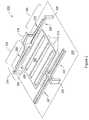
- anchor base 1100is securely attached to the substrate.
- sidewall well 1102is comprised of several NHEP sidewalls and provides the critical rise in elevation of the beams above the substrate.
- Shelf 1104is coupled to the top of the sidewall well 1102 .
- a set of NHSSP sidewalls 1105couples to shelf 1104 and 1106 , which in turn couples to NHSSP 1108 and then to shelf 1110 .
- This corrugated structure formed by the intersections of NHSSP sidewalls and shelvesprovide improved resistance to deflection and torsion of beam 1004 and 1006 , i.e. an enhancement of the second and polar moments of inertia.
- an anchorcan be constructed in which the three-sided sidewall 1105 and 1108 and shelf 1106 are not continuous. In other words, there is a break in 1105 , 1108 , and 1106 along the symmetry axis of the anchor.
- the looped ends of the drive beams ( 1004 , 1006 )tend to deflect towards the substrate under certain stresses.
- the resulting deflection down in elevation at the looped end of the beamshas been shown to be as much as 1.5 micrometers.
- Such a downward deflectioncould cause the drive beams to touch the substrate, hindering the movement of the beams.
- the drive beamsmay tend to deflect away from the substrate. Any out-of-plane deflection would misalign the drive beams ( 1004 , 1006 ) to the shutter load beams ( 1008 , 1010 ) and would reduce the electrostatic force between them and impair actuation.
- the addition of the continuous sidewall and shelf combinationcreates a stiffer anchor, more resistant to deflection and torsion, as seen in FIG. 18B .
- an additional shelf 1110is formed that couples to sidewall 1108 and to sidewall 1112 , which continues and connects to outside loop sidewall 1116 and couples to shelf 1114 .
- the substantially orthogonal sidewall-shelf combinationscreate a corrugation effect that translates into an enhancement of the second moment of inertia of the anchor of drive beams 1004 and 1006 .
- the drive beamshas been shown to deflect out-of-plane by only 0.15 micrometers.
- the inclusion of anchors with structures implementing two or more perpendicular wall-shelf combinationscreates a solid base for the compliant beam that resists flexing and torsion along the beam.
- spaceis efficiently used by making the width of shelf 1104 (that is, the distance connecting sidewall 1105 to the sidewall well less than 100 times the thickness of the side beam. This results in a small anchor footprint with minimal distance between parallel walls.
- FIG. 15illustrates an embodiment of shutter anchor 1012 , which is the anchor for shutter load beam 1008 .
- This anchoris a mirror of anchor 1014 .
- the anchor base 1200is attached to the substrate, and the anchor bottom well is formed by the NHEP sidewall 1202 , which is coupled to base 1200 .
- Shelf 1204is coupled to NHEP sidewall well 1202 and serves as the base for the NHSSP sidewall 1206 .
- the compliant shutter load beam 1008is coupled to NHSSP sidewall 1206 .
- the coupling of the substantially orthogonal shelf-sidewall combinationsserves to stiffen (by increasing its second and polar moments of inertia) the anchoring point for compliant shutter load beam 1008 .
- a stiffer anchorresists torsion and vertical deflection of the compliant shutter load beam 1008 from its own stresses or that of the shutter.
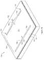
- FIG. 16depicts a trimetric projection of a possible embodiment of the two-spring shutter seen in FIG. 5 .
- a drive beam ( 526 , 528 ) that is attached to an anchor ( 522 , 524 )is designed to electrostatically attract a compliant shutter load beam ( 502 , 503 ), which is attached to an anchor ( 508 , 506 ) and shutter 504 at a shutter connection point ( 510 , 512 ).
- the compliant load beam ( 502 , 503 ) of the two-spring embodimentspans the complete shutter structure 504 . While efficient, a longer beam tends to amplify any undesirable behavior due to torsional or deflection effects of drive beams ( 526 , 528 ), load beams ( 502 , 503 ), and shutter 504 .
- the critical area for supporting the load beam 502occurs at anchor point 508 .
- the anchoris made stiffer by the inclusion of two perpendicular shelf-sidewall combinations in a fashion similar to that described in FIG. 15 above.
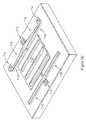
- FIG. 17is a close-up of an illustrative embodiment of drive beam anchor 522 from FIG. 16 in a two-spring embodiment.
- the drive beam anchoris attached to the substrate by two anchor bases ( 1402 , 1404 ), around which NHEP sidewall wells ( 1406 , 1408 ) are coupled.
- Shelves ( 1410 , 1412 )are coupled to the NHEP sidewall wells around their periphery.
- NHSSP sidewall 1414couples to and connects shelves ( 1410 , 1412 ) and continues around to form the looped drive beam 526 .
- An additional shelf 1416is connected on top of NHSSP 1414 , which provides additional anchor stiffness.
Landscapes
- Physics & Mathematics (AREA)
- General Physics & Mathematics (AREA)
- Optics & Photonics (AREA)
- Engineering & Computer Science (AREA)
- Computer Hardware Design (AREA)
- Microelectronics & Electronic Packaging (AREA)
- Mechanical Light Control Or Optical Switches (AREA)
Abstract
Description
This application is a continuation of U.S. application Ser. No. 12/606,675, filed Oct. 27, 2009 which claims the benefit of U.S. Provisional Patent Application Ser. No. 61/108,783, filed on Oct. 27, 2008, entitled “MEMS Anchors”, which is incorporated by reference herein in its entirety.
The present invention generally relates to the field of displays, such as imaging and projection displays. In particular, the invention relates to the design and manufacture of anchor structures for light modulators to address the deflection of beams mounted on them.
There is a need in the art for fast, bright, low-powered actuated displays. Displays built from mechanical light modulators are an attractive alternative to displays based on liquid crystal technology. Mechanical light modulators are fast enough to display video content with good viewing angles and with a wide range of color and grey scale. Mechanical light modulators have been successful in projection display applications, and have recently been proposed for direct view applications. Specifically there is a need for mechanically actuated displays that use mechanical light modulators and can be driven at high speeds and at low voltages for improved image quality and reduced power consumption.
A mechanical light modulator comprises a shutter and a plurality of actuators. The actuators are used to move the shutter from one state to another state. Of the two states, one can be a state where light is transmitted and another state where light is blocked. The shutter is suspended above a substrate by a plurality of compliant beams, and the actuators are also formed using compliant beams. A display is formed by fabricating an array of mechanical light modulators on a substrate. The compliant beams are attached to the substrate with anchor structures.
The anchor structures need to be sufficiently stiff to limit undesired deflections of the actuators and of the shutter. An example of an undesired deflection would be a deflection towards or away from the substrate for a shutter that is designed to move parallel to the substrate. Such a deflection can occur due to mechanical shock applied to the shutter or due to attraction between the shutter and the substrate. A deflection can also be caused by stresses in the films that are used to form the shutter, the actuators, and the anchors
A need exists in the art for an anchoring structure for these compliant beams that can be built using MEMS fabrication techniques while at the same time preventing or minimizing any undesired beam or shutter deflection.
This section is for the purpose of summarizing some aspects of the present invention and to briefly introduce some preferred embodiments. Simplifications or omissions may be made to avoid obscuring the purpose of the section. Such simplifications or omissions are not intended to limit the scope of the present invention.
In one aspect, the present invention relates to a MEMS device comprising a substrate having a primary surface upon which the MEMS device is formed, a beam suspended over the substrate by an anchor having a shell structure, the shell structure comprising: a non-horizontal elevating portion is coupled (or connected) to the primary face of the substrate, a substantially horizontal shelf portion elevated over the substrate by the non-horizontal elevating portion, and a non-horizontal shell stiffening portion, from which the beam extends, extending from the shelf portion.
In some embodiments a shutter being connected to the beams. In one embodiment, this is accomplished by coupling the beam to a plurality of beams, each connected to its own anchor. In another aspect, the invention relates to an anchoring structure where the non-horizontal shell stiffening portion comprises at least two unit normal vectors that are substantially different. In another aspect, the invention relates to an anchoring structure where at least two non-horizontal shell stiffening portions are coupled to each other as well as to the substantially horizontal shelf portion and where the normal vectors of said non-horizontal shell stiffening portions are substantially different. In another aspect, the invention relates to an anchoring structure where one or more substantially horizontal shelf portions are further coupled to one or more non-horizontal shell stiffening portions. In some embodiments, the non-horizontal elevating portions form a closed space or a well. In another aspect, the invention relates to an anchoring structure where the suspended beam has a height that is at least 1.4 times its width. In another aspect, the invention relates to an anchoring structure where the non-horizontal stiffening portion is made from the same material as the horizontal shelf portion. In another aspect, the invention relates to an anchoring structure where the beam is made from a different material than the horizontal shelf portion. In some embodiments, the beam is couple to the horizontal portion. In certain embodiments, two or more beams extend from the anchor structure. In one aspect, the non-horizontal shell stiffening portion extends above the shelf. In another aspect, the non-horizontal shell stiffening portion extends below the shelf. In certain embodiments, the beam is situated on the side of the horizontal shelf opposite to the substrate. In one aspect, the non-horizontal shell stiffening portion is substantially perpendicular to the horizontal shelf portion.
In another aspect, the invention relates to a method for manufacturing a MEMS device using a shell structure made by a sidewall process comprising the steps of forming a mold on a substrate, wherein the mold includes a lower horizontal surface, an upper horizontal surface and a wall, depositing a beam material on the lower horizontal surface and the wall of the mold, removing the beam material deposited on the lower horizontal surface of the mold while leaving the majority of the beam material deposited on the wall of the mold in place to form the compliant beam, forming the shutter coupled to the compliant beam, and removing the mold, thereby releasing the shutter and remaining beam material.
In some embodiments, the non-horizontal elevating portion is manufactured from a first mold material. In some embodiments, the non-horizontal elevating portion is manufactured from a second mold material. In one aspect, the shell structure and the beam are manufactured from at least two different materials. In certain embodiments, the shell structure and the beam are manufactured from a composite material.
Other objects, features and advantages of the present invention will become apparent upon examining the following detailed description of an embodiment thereof, taken in conjunction with the attached drawings. The present invention may be implemented in many forms including a device, method, or part of a device.
The foregoing discussion will be understood more readily from the following detailed description of the invention with reference to the following drawings
To provide an overall understanding of the invention, certain illustrative embodiments will now be described, including apparatus and methods for displaying images. However, it will be understood by one of ordinary skill in the art that the systems and methods described herein may be adapted and modified as is appropriate for the application being addressed and that the systems and methods described herein may be employed in other suitable applications, and that such other additions and modifications will not depart from the scope hereof.
In thedisplay apparatus 100, each light modulator102 corresponds to apixel 106 in theimage 104. In other implementations, thedisplay apparatus 100 may utilize a plurality of light modulators to form apixel 106 in theimage 104. For example, thedisplay apparatus 100 may include three color-specific light modulators102. By selectively opening one or more of the color-specific light modulators102 corresponding to aparticular pixel 106, thedisplay apparatus 100 can generate acolor pixel 106 in theimage 104. In another example, thedisplay apparatus 100 includes two or more light modulators102 perpixel 106 to provide grayscale in animage 104. With respect to an image, a “pixel” corresponds to the smallest picture element defined by the resolution of the image. With respect to structural components of thedisplay apparatus 100, the term “pixel” refers to the combined mechanical and electrical components utilized to modulate the light that forms a single pixel of the image.
Direct-view displays may operate in either a transmissive or reflective mode. In a transmissive display, the light modulators filter or selectively block light which originates from a lamp or lamps positioned behind the display. The light from the lamps is optionally injected into a light guide or “backlight”. Transmissive direct-view display embodiments are often built onto transparent or glass substrates to facilitate a sandwich assembly arrangement where one substrate, containing the light modulators, is positioned directly on top of the backlight. In some transmissive display embodiments, a color specific light modulator is created by associating a color filter material with each modulator102. In other transmissive display embodiments colors can be generated, as described below, using a field sequential color method by alternating illumination of lamps with different primary colors.
Each light modulator102 includes ashutter 108 and anaperture 109. To illuminate apixel 106 in theimage 104, theshutter 108 is positioned such that it allows light to pass through theaperture 109 towards a viewer. To keep apixel 106 unlit, theshutter 108 is positioned such that it obstructs the passage of light through theaperture 109. Theaperture 109 is defined by an opening patterned through a reflective or light absorbing material. The display apparatus also includes a control matrix connected to the substrate and to the light modulators for controlling the movement of the shutters. The control matrix includes a series of electrical interconnects (e.g., interconnects110,112, and114), including at least one write-enable interconnect110 (also referred to as a “scan-line interconnect”) per row of pixels, onedata interconnect 112 for each column of pixels, and onecommon interconnect 114 providing a common voltage to all pixels, or at least to pixels from both multiple columns and multiples rows in thedisplay apparatus 100. In response to the application of an appropriate voltage (the “write-enabling voltage, Vwe”), the write-enableinterconnect 110 for a given row of pixels prepares the pixels in the row to accept new shutter movement instructions. The data interconnects112 communicate the new movement instructions in the form of data voltage pulses. The data voltage pulses applied to the data interconnects112, in some implementations, directly contribute to an electrostatic movement of the shutters. In other implementations, the data voltage pulses control switches, e.g., transistors or other non-linear circuit elements that control the application of separate actuation voltages, which are typically higher in magnitude than the data voltages, to the light modulators102. The application of these actuation voltages then results in the electrostatic driven movement of theshutters 108.
MEMS Light Modulators
Eachactuator 205 includes acompliant load beam 206 connecting theshutter 202 to aload anchor 208. The load anchors208 along with the compliant load beams206 serve as mechanical supports, keeping theshutter 202 suspended proximate to thesurface 203. The load anchors208 physically connect the compliant load beams206 and theshutter 202 to thesurface 203 and electrically connect the load beams206 to a bias voltage, in some instances, ground.
Eachactuator 205 also includes acompliant drive beam 216 positioned adjacent to eachload beam 206. The drive beams216 couple at one end to adrive beam anchor 218 shared between the drive beams216. The other end of eachdrive beam 216 is free to move. Eachdrive beam 216 is curved such that it is closest to theload beam 206 near the free end of thedrive beam 216 and the anchored end of theload beam 206.
Thesurface 203 includes one ormore apertures 211 for admitting the passage of light. If theshutter assembly 200 is formed on an opaque substrate, made for example from silicon, then thesurface 203 is a surface of the substrate, and theapertures 211 are formed by etching an array of holes through the substrate. If theshutter assembly 200 is formed on a transparent substrate, made for example of glass or plastic, then thesurface 203 is a surface of a light blocking layer deposited on the substrate, and the apertures are formed by etching thesurface 203 into an array ofholes 211. Theapertures 211 can be generally circular, elliptical, polygonal, serpentine, or irregular in shape.
In operation, a display apparatus incorporating thelight modulator 200 applies an electric potential to the drive beams216 via thedrive beam anchor 218. A second electric potential may be applied to the load beams206. The resulting potential difference between the drive beams216 and the load beams206 pulls the free ends of the drive beams216 towards the anchored ends of the load beams206, and pulls the shutter ends of the load beams206 toward the anchored ends of the drive beams216, thereby driving theshutter 202 transversely towards thedrive anchor 218. Thecompliant members 206 act as springs, such that when the voltage across thebeams shutter 202 back into its initial position, releasing the stress stored in the load beams206.
Theshutter assembly 200, also referred to as an elastic shutter assembly, incorporates a passive restoring force, such as a spring, for returning a shutter to its rest or relaxed position after voltages have been removed. A number of elastic restore mechanisms and various electrostatic couplings can be designed into or in conjunction with electrostatic actuators, the compliant beams illustrated inshutter assembly 200 being just one example. Other examples are described in Hagood et al (U.S. Pat. No. 7,271,945), and U.S. patent application Ser. No. 11/326,696, both incorporated herein by reference in their entirety. For instance, a highly non-linear voltage-displacement response can be provided which favors an abrupt transition between “open” vs. “closed” states of operation, and which, in many cases, provides a bi-stable or hysteretic operating characteristic for the shutter assembly. Other electrostatic actuators can be designed with more incremental voltage-displacement responses and with considerably reduced hysteresis, as may be preferred for analog gray scale operation.
Theactuator 205 within the elastic shutter assembly is said to operate between a closed or actuated position and a relaxed position. The designer, however, can choose to placeapertures 211 such thatshutter assembly 200 is in either the “open” state, i.e. passing light, or in the “closed” state, i.e. blocking light, wheneveractuator 205 is in its relaxed position. For illustrative purposes, it is assumed below that elastic shutter assemblies described herein are designed to be open in their relaxed state.
In many cases it is preferable to provide a dual set of “open” and “closed” actuators as part of a shutter assembly so that the control electronics are capable of electrostatically driving the shutters into each of the open and closed states.
It will be understood that other MEMS light modulators can exist and can be usefully incorporated into the invention. Both Hagood et al (U.S. Pat. No. 7,271,945 and U.S. patent application Ser. No. 11/326,696 (both incorporated herein by reference in their entirety) have described a variety of methods by which an array of shutters can be controlled via a control matrix to produce images, in many cases moving images, with appropriate gray scale. In some cases, control is accomplished by means of a passive matrix array of row and column interconnects connected to driver circuits on the periphery of the display. In other cases it is appropriate to include switching and/or data storage elements within each pixel of the array (the so-called active matrix) to improve either the speed, the gray scale and/or the power dissipation performance of the display.
Referring toFIG. 3 , control matrix300 is fabricated as a diffused or thin-film-deposited electrical circuit on the surface of asubstrate 304 on which theshutter assemblies 302 are formed. The control matrix300 includes a scan-line interconnect 306 for each row ofpixels 301 in the control matrix300 and a data-interconnect 308 for each column ofpixels 301 in the control matrix300. Each scan-line interconnect 306 electrically connects a write enabling voltage source307 to thepixels 301 in a corresponding row ofpixels 301. Eachdata interconnect 308 electrically connects a data voltage source, (“Vdsource”)309 to thepixels 301 in a corresponding column ofpixels 301. In control matrix300, the data voltage Vdprovides the majority of the energy necessary for actuation of theshutter assemblies 302. Thus, the data voltage source309 also serves as an actuation voltage source.
For eachpixel 301 or for eachshutter assembly 302 in the array ofpixels 320, the control matrix300 includes atransistor 310 and acapacitor 312. The gate of eachtransistor 310 is electrically connected to the scan-line interconnect 306 of the row in thearray 320 in which thepixel 301 is located. The source of eachtransistor 310 is electrically connected to itscorresponding data interconnect 308. Theactuators 303 of eachshutter assembly 302 include two electrodes. The drain of eachtransistor 310 is electrically connected in parallel to one electrode of thecorresponding capacitor 312 and to one of the electrodes of thecorresponding actuator 303. The other electrode of thecapacitor 312 and the other electrode of theactuator 303 inshutter assembly 302 are connected to a common or ground potential. In alternate implementations, thetransistors 310 can be replaced with semiconductor diodes and or metal-insulator-metal sandwich type switching elements.
In operation, to form an image, the control matrix300 write-enables each row in thearray 320 in a sequence by applying Vweto each scan-line interconnect 306 in turn. For a write-enabled row, the application of Vweto the gates of thetransistors 310 of thepixels 301 in the row allows the flow of current through the data interconnects308 through thetransistors 310 to apply a potential to theactuator 303 of theshutter assembly 302. While the row is write-enabled, data voltages Vdare selectively applied to the data interconnects308. In implementations providing analog gray scale, the data voltage applied to eachdata interconnect 308 is varied in relation to the desired brightness of thepixel 301 located at the intersection of the write-enabled scan-line interconnect 306 and thedata interconnect 308. In implementations providing digital control schemes, the data voltage is selected to be either a relatively low magnitude voltage (i.e., a voltage near ground) or to meet or exceed Vat (the actuation threshold voltage). In response to the application of Vat to adata interconnect 308, theactuator 303 in thecorresponding shutter assembly 302 actuates, opening the shutter in thatshutter assembly 302. The voltage applied to thedata interconnect 308 remains stored in thecapacitor 312 of thepixel 301 even after the control matrix300 ceases to apply Vweto a row. It is not necessary, therefore, to wait and hold the voltage Vweon a row for times long enough for theshutter assembly 302 to actuate; such actuation can proceed after the write-enabling voltage has been removed from the row. Thecapacitors 312 also function as memory elements within thearray 320, storing actuation instructions for periods as long as is necessary for the illumination of an image frame.
Thepixels 301 as well as the control matrix300 of thearray 320 are formed on asubstrate 304. The array includes anaperture layer 322, disposed on thesubstrate 304, which includes a set ofapertures 324 forrespective pixels 301 in thearray 320. Theapertures 324 are aligned with theshutter assemblies 302 in each pixel. In one implementation thesubstrate 304 is made of a transparent material, such as glass or plastic. In another implementation thesubstrate 304 is made of an opaque material, but in which holes are etched to form theapertures 324.
Components ofshutter assemblies 302 are processed either at the same time as the control matrix300 or in subsequent processing steps on the same substrate. The electrical components in control matrix300 are fabricated using many thin film techniques in common with the manufacture of thin film transistor arrays for liquid crystal displays. Available techniques are described in Den Boer, Active Matrix Liquid Crystal Displays (Elsevier, Amsterdam, 2005), incorporated herein by reference. The shutter assemblies are fabricated using techniques similar to the art of micromachining or from the manufacture of micromechanical (i.e., MEMS) devices. Many applicable thin film MEMS techniques are described in Rai-Choudhury, ed., Handbook of Microlithography, Micromachining & Microfabrication (SPIE Optical Engineering Press, Bellingham, Wash. 1997), incorporated herein by reference. Fabrication techniques specific to MEMS light modulators formed on glass substrates can be found in Brosnihan (U.S. Pat. No. 7,405,852) and U.S. application Ser. No. 11/731,628, both incorporated herein by reference in their entirety. For instance, as described in those applications, theshutter assembly 302 can be formed from thin films of amorphous silicon, deposited by a chemical vapor deposition process.
Theshutter assembly 302 together with theactuator 303 can be made bi-stable. That is, the shutters can exist in at least two equilibrium positions (e.g. open or closed) with little or no power required to hold them in either position. More particularly, theshutter assembly 302 can be mechanically bi-stable. Once the shutter of theshutter assembly 302 is set in position, no electrical energy or holding voltage is required to maintain that position. The mechanical stresses on the physical elements of theshutter assembly 302 can hold the shutter in place.
Theshutter assembly 302 together with theactuator 303 can also be made electrically bi-stable. In an electrically bi-stable shutter assembly, there exists a range of voltages below the actuation voltage of the shutter assembly, which if applied to a closed actuator (with the shutter being either open or closed), holds the actuator closed and the shutter in position, even if an opposing force is exerted on the shutter. The opposing force may be exerted by a spring such asspring 207 in shutter-basedlight modulator 200, or the opposing force may be exerted by an opposing actuator, such as an “open” or “closed” actuator.
Thelight modulator array 320 is depicted as having a single MEMS light modulator per pixel. Other embodiments are possible in which multiple MEMS light modulators are provided in each pixel, thereby providing the possibility of more than just binary “on” or “off” optical states in each pixel. Certain forms of coded area division gray scale are possible where multiple MEMS light modulators in the pixel are provided, and whereapertures 324, which are associated with each of the light modulators, have unequal areas.
In other embodiments the roller-based light modulator220 and the light tap250, as well as other MEMS-based light modulators, can be substituted for theshutter assembly 302 within thelight modulator array 320.
Theshutter 406 includes twoshutter apertures 412 through which light can pass. Theaperture layer 407 includes a set of threeapertures 409. InFIG. 4A , theshutter assembly 400 is in the open state and, as such, the shutter-open actuator 402 has been actuated, the shutter-close actuator 404 is in its relaxed position, and the centerlines ofapertures FIG. 4B theshutter assembly 400 has been moved to the closed state and, as such, the shutter-open actuator 402 is in its relaxed position, the shutter-close actuator 404 has been actuated, and the light blocking portions ofshutter 406 are now in position to block transmission of light through the apertures409 (shown as dotted lines).
Each aperture has at least one edge around its periphery. For example, therectangular apertures 409 have four edges. In alternative implementations in which circular, elliptical, oval, or other curved apertures are formed in theaperture layer 407, each aperture may have only a single edge. In other implementations the apertures need not be separated or disjoint in the mathematical sense, but instead can be connected. That is to say, while portions or shaped sections of the aperture may maintain a correspondence to each shutter, several of these sections may be connected such that a single continuous perimeter of the aperture is shared by multiple shutters.
In order to allow light with a variety of exit angles to pass throughapertures shutter apertures 412 which is larger than a corresponding width or size ofapertures 409 in theaperture layer 407. In order to effectively block light from escaping in the closed state, it is preferable that the light blocking portions of theshutter 406 overlap theapertures 409.FIG. 4B shows apredefined overlap 416 between the edge of light blocking portions in theshutter 406 and one edge of theaperture 409 formed inaperture layer 407.
Theelectrostatic actuators shutter assembly 400. For each of the shutter-open and shutter-close actuators there exists a range of voltages below the actuation voltage, which if applied while that actuator is in the closed state (with the shutter being either open or closed), will hold the actuator closed and the shutter in position, even after an actuation voltage is applied to the opposing actuator. The minimum voltage needed to maintain a shutter's position against such an opposing force is referred to as a maintenance voltage Vm. A number of control matrices which take advantage of the bistable operation characteristic are described in U.S. patent application Ser. No. 11/607,715, referenced above.
The shelves within the anchor structures create a reference plane above the substrate to which the load beams are attached. This elevation and connection to the shutter through the load beams (502,503) help to suspend the shutter504 a specified distance above the surface. Notice that in one embodiment, these attachment points (510,512) are on opposite sides of theshutter 504. This embodiment has demonstrated advantages in keeping the shutter from rotating around the axis normal to the substrate surface upon actuation. In other embodiments, the load beams are connected to the other corners of the shutter.
The drive beams (526,528) are similarly suspended above the surface of the substrate by their anchor structures (522,524). In operation, the shutter moves from one position to another by the electric attraction of its load beams (502,503) to their respective drive beams (526,528). To move theshutter 504 towardsdrive beam 526, we set the potential ofdrive beam 526 to a different value than the potential ofshutter 504, while keepingdrive beam 528 the same potential asshutter 504. Conversely, to drive the shutter in the towardsdrive beam 528, we set the potential ofdrive beam 528 to a different value than the potential ofshutter 504, while keepingdrive beam 526 the same potential asshutter 504. These drive beams are cantilevered beams that are each attached to a respective anchor (522,524). More is discussed about these inFIGS. 8A and 8B .
Theshutter 504 is disposed on a transparent substrate preferably made of glass or plastic. A rear-facing reflective layer disposed on the substrate below the shutter defines a plurality of surface apertures located beneath the shutter. The vertical gap that separates the shutter from the underlying substrate is in the range of 0.1 to 10 microns. The magnitude of the vertical gap is preferably less than the lateral overlap between the edge of shutter and the edge of aperture in the closed state, such as theoverlap 416 shown inFIG. 4B .
Shutter Manufacturing
In some implementations the order of the layers incomposite shutter assembly 600 can be inverted, such that the outside of the sandwich is comprised of a conducting layer while the inside of the sandwich is comprised of a mechanical layer.
Further description of materials for use inshutter 601, including the incorporation of materials selected for the absorption or reflection of incident light can be found in Brosnihan (U.S. Pat. No. 7,405,852) incorporated herein in its entirety by reference.
Next thesacrificial layer 613 is patterned to expose holes or vias at theanchor regions 604. The preferred polyimide material and other polymer resins can be formulated to include photoactive agents—enabling regions exposed through a UV photomask to be preferentially removed in a developer solution. Othersacrificial layers 613 can be patterned by coating the sacrificial layer in an additional layer of photoresist, photopatterning the photoresist, and finally using the photoresist as an etching mask. Other sacrificial layers can be patterned by coating the sacrificial layer with a hard mask, which can be a thin layer of SiO2or metal such as chromium. A photopattern is then transferred to the hard mask by means of photoresist and wet chemical etching. The pattern developed in the hard mask can be very resistant to dry chemical, anisotropic, or plasma etching—techniques which can be used to impart very deep and narrow anchor holes into the sacrificial layer.
After theanchor 604 or via regions have been opened in the sacrificial layer, the exposed and underlying conductingsurface 614 can be etched, either chemically or via the sputtering effects of a plasma, to remove any surface oxide layers. Such a contact etching step can improve the ohmic contact between the underlying conductor and the shutter material.
After patterning of the sacrificial layer, any photoresist layers or hard masks can be removed through use of either solvent cleans or acid etching.
Next, in the process for buildingshutter assembly 600, as shown inFIG. 6C , the shutter materials are deposited. Theshutter assembly 600 is composed of multiplethin films mechanical layer 605 is an amorphous silicon layer, deposited first, followed by aconductor layer 607 comprised of aluminum, followed by asecond layer 609 of amorphous silicon. The deposition temperature used for theshutter materials shutter materials layers mechanical layer 605 or for the deposition of diamond-like carbon, Ge, SiGe, CdTe, or other semiconducting materials formechanical layer oxynitride 605. An advantage of the PECVD deposition technique is that the deposition can be quite conformal, that is, it can coat a variety of inclined surfaces or the inside surfaces of narrow via holes. Even if the anchor or via holes which are cut into the sacrificial material present nearly vertical sidewalls, the PECVD technique can provide a continuous coating between the bottom and top horizontal surfaces of the anchor.
In addition to the PECVD technique, alternate techniques available for the growth of shutter layers605 or609 include RF or DC sputtering, metal-organic chemical vapor deposition, evaporation, electroplating or electroless plating.
For theconducting layer 607, a metal thin film such as Al is preferred, although alternates such as Cu, Ni, Mo, or Ta can be chosen. The inclusion of such a conducting material serves two purposes. It reduces the overall sheet resistance of the shutter material and it helps to block the passage of visible light through the shutter material. (Amorphous silicon can be doped to be conductive, however, if grown to thicknesses of less than 2 microns can transmit visible light to some degree.) The conducting material can be deposited either by sputtering or, in a more conformal fashion, by chemical vapor deposition techniques, electroplating, or electroless plating.
The process for building theshutter assembly 600 continues inFIG. 6D . The shutter layers605,607, and609 are photomasked and etched while thesacrificial layer 613 is still on the wafer. First a photoresist material is applied, then exposed through a photomask, and then developed to form an etch mask. Amorphous silicon, silicon nitride, and silicon oxide can then be etched in fluorine-based plasma chemistries. SiO2mechanical layers can be etched using HF wet chemicals; and any metals in the conductor layers can be etched with either wet chemicals or chlorine-based plasma chemistries.
The pattern shapes applied through the photomask atFIG. 6D influence the mechanical properties, such as stiffness, compliance, and the voltage response in the actuators and shutters of theshutter assembly 600. Theshutter assembly 600 includes acompliant beam 602, shown in cross section.Compliant beam 602 is shaped such that the width is less than the total height or thickness of the shutter material. It is preferable to maintain a beam dimensional ratio of at least 1.4:1, with thebeams 602 being taller or thicker than they are wide.
The process for building theshutter assembly 600 continues as depicted inFIG. 6E . Thesacrificial layer 613 is removed, which frees-up all moving parts from thesubstrate 603, except at the anchor points. Polyimide sacrificial materials are preferably removed in an oxygen plasma. Other polymer materials used forsacrificial layer 613 can also be removed in an oxygen plasma, or in some cases by thermal pyrolysis. Some sacrificial layers613 (such as SiO2) can be removed by wet chemical etching or by vapor phase etching.
In a final process, not shown inFIG. 6E but shown inFIG. 6A , adielectric coating 611 is deposited on all exposed surfaces of the shutter.Dielectric coatings 611 can be applied in conformal fashion, such that all bottom, tops, and side surfaces of theshutters 601 andbeams 602 are uniformly coated using chemical vapor deposition. Al2O3is a preferred dielectric coating forlayer 611, which is deposited by atomic layer deposition to thicknesses in the range of 10 to 100 nanometers.
Finally, anti-stiction coatings can be applied to the surfaces of allshutters 601 and beams602. These coatings prevent the unwanted stickiness or adhesion between two independent beams of an actuator. Applicable coatings include carbon films (both graphite and diamond-like) as well as fluoropolymers, and/or low vapor pressure lubricants. These coatings can be applied by either exposure to a molecular vapor or by decomposition of a precursor compounds by means of chemical vapor deposition. Anti-stiction coatings can also be created by the chemical alteration of shutter surfaces, as in the fluoridation, silanization, siloxidation, or hydrogenation of insulating surfaces.
The Sidewall Beams Process
U.S. Pat. No. 7,271,945, incorporated herein by reference in its entirety, describes a number of useful designs for shutter assemblies and actuators. One class of suitable actuators for use in MEMS-based shutter displays include compliant actuator beams for controlling shutter motion that is transverse to or in-the-plane of the display substrate. The voltage necessary for the actuation of such shutter assemblies decreases as the actuator beams become more compliant. The control of actuated motion also improves if the beams are shaped such that in-plane motion is preferred or promoted with respect to out-of-plane motion. In a preferred design the compliant actuator beams have a rectangular cross section, such asbeam 602 ofFIG. 6A , such that the beams are taller or thicker than they are wide.
The stiffness of a long rectangular beam with respect to bending within a particular plane scales with the thinnest dimension of that beam in that plane to the third power. It is of interest, therefore, to reduce the width of the compliant beams as far as possible to reduce the actuation voltages for in-plane motion. When using conventional photolithography equipment to define and fabricate the shutter and actuator structures, however, the minimum width of the beams is usually limited to the resolution of the exposure optics. And although photolithography equipment has been developed for defining patterns in photoresist with features as narrow as 15 nanometers, such equipment is expensive and the areas over which patterning can be accomplished in a single exposure are limited. For economical photolithography over large panels of glass, the patterning resolution or minimum feature size is typically limited to 1 micron or 2 microns or greater.
U.S. Patent Application Publication No. US 2007/0002156 describes a technique, illustrated inFIGS. 7A through 7D , whereby ashutter assembly 700 with compliant actuator beams716 can be fabricated at dimensions well below the conventional lithography limits on large glass panels. In the process ofFIGS. 7A through 7D , the compliant beams ofshutter assembly 700 are formed as sidewall features on a mold made from a sacrificial material. The process is referred to as a sidewall beams process.
The process of forming ashutter assembly 700 with sidewall beams begins, as shown inFIG. 7A , with the deposition and patterning of a firstsacrificial material 701. The pattern defined in the first sacrificial material creates openings orvias 702 within which anchors for the shutter will eventually be formed. The deposition and patterning of the firstsacrificial material 701 is similar in concept, and uses similar materials, as those described for the deposition and patterning described in relation toFIGS. 6A-6E .
The process of forming sidewall beams continues with the deposition and patterning of a secondsacrificial material 705.FIG. 7B shows the shape of amold 703 that is created after patterning of the secondsacrificial material 705. Themold 703 also includes the firstsacrificial material 701 with its previously definedvias 702. Themold 703 inFIG. 7B includes two distinct horizontal levels: The bottomhorizontal level 708 ofmold 703 is established by the top surface of the firstsacrificial layer 701 and is accessible in those areas where the secondsacrificial layer 705 has been etched away. The tophorizontal level 710 of themold 703 is established by the top surface of the secondsacrificial layer 705. Themold 703 illustrated inFIG. 7B also includes substantiallyvertical sidewalls 709.
Materials for use assacrificial materials sacrificial material 613.
The process of forming sidewall beams continues with the deposition and patterning of the shutter material onto all of the exposed surfaces of thesacrificial mold 703, as depicted inFIG. 7C . The preferred materials for use inshutter 712 are described above with respect to theshutter materials FIG. 7C . The pattern developed into the photoresist is designed such that shutter material remains in the region ofshutter 712 as well as at theanchors 714.
Particular equipment and chemistries are also chosen for the etching process used at the step shown inFIG. 7C , known in the art as an anisotropic etch. The anisotropic etch of the shutter material is carried out in a plasma atmosphere with a voltage bias applied to the substrate, or to an electrode in proximity to the substrate. The biased substrate (with electric field perpendicular to the surface of the substrate) leads to acceleration of ions toward the substrate at an angle nearly perpendicular to the substrate. Such accelerated ions, coupled with the etching chemicals, lead to etch rates that are much faster in a direction that is normal to the plane of the substrate as compared to directions parallel to the substrate. Undercut-etching of shutter material in the regions protected by photoresist is thereby substantially eliminated. Along sidewall surfaces709 ofmold 703, which are substantially parallel to the track of the accelerated ions, the shutter material is also substantially protected from the anisotropic etch. Such protected sidewall shutter material will later formcompliant beams 716 for supporting theshutter 712. Along other (non-photoresist-protected) horizontal surfaces of the mold, such as tophorizontal surface 710 or bottomhorizontal surface 708, the shutter material has been completely removed by the etch.
The anisotropic etch used to form sidewall beams716 can be achieved in either an RF or DC plasma etching device as long as provision for electrical bias of the substrate, or of an electrode in close proximity of the substrate, is supplied. For the case of RF plasma etching, an equivalent self-bias can be obtained by disconnecting the substrate holder from the grounding plates of the excitation circuit, thereby allowing the substrate potential to float in the plasma. In one implementation it is possible to provide an etching gas such as CHF3, C4F8, or CHCl3in which both carbon and hydrogen and/or carbon and fluorine are constituents in the etch gas. When coupled with a directional plasma, achieved again through voltage biasing of the substrate, the liberated C, H, and/or F atoms can migrate to thesidewalls 709 where they build up a passive or protective quasipolymer coating. This quasi-polymer coating further protects the sidewall beams716 from etching or chemical attack.
The process of forming sidewall beams is completed with the removal of the remainder of the secondsacrificial layer 705 and the firstsacrificial layer 701, the result being shown inFIG. 7D . The process of removing sacrificial material is similar to that described with respect toFIG. 6E . The material deposited on thesidewalls 709 of themold 703 remain as the compliant beams716. Thecompliant beams 716 mechanically connect theanchors 714 to theshutter 712. The anchors connect to an aperture layer725. Thecompliant beams 716 are tall and narrow. The width of the sidewall beams716, as formed from the surface of themold 703, is similar to the thickness of the shutter material as deposited. In some cases the beam width at716 will be the same as the thickness of the horizontal shutter material at712, in other cases the beam width will be only about ½ the thickness of the shutter material. The height of the sidewall beams716 is determined by the thickness of the secondsacrificial material 705, or in other words, by the depth of themold 703 as created during the patterning step described in relation toFIG. 7B . As long as the thickness of the deposited shutter material is chosen to be less than 2 microns (for many applications the thickness range of 0.1 to 2.0 micron is suitable), the method illustrated inFIGS. 7A-7D is well suited for the production of very narrow beams. Conventional photolithography would limit the patterned features shown inFIGS. 7A ,7B, and7C to much larger dimensions, for instance allowing minimum resolved features no smaller than 2 microns or 5 microns.
An optional step, not illustrated above but included as part of the process leading toFIG. 7C , involves isotropic etching ofsidewall beams 716 to separate or decouple beams formed along the sidewalls ofmold 703. For instance, the shutter material atpoint 724 has been removed from the sidewall through use of an in isotropic etch. An isotropic etch is one whose etch rate is the same in all directions, so that sidewall material in regions such aspoint 724 is no longer protected. The isotropic etch can be accomplished in the typical plasma etch equipment as long as a bias voltage is not applied to the substrate. Isotropic etch can also be achieved using wet chemical or vapor phase etching techniques. The separation of beams atpoint 724 is achieved through a distinct sequence of photoresist dispense, patterning, and etch. The photoresist pattern in this case is designed to protect the sidewall beams716 from the isotropic etch chemistry but expose the sidewall beams atpoint 724.
As a final step in the sidewall process, an encapsulating dielectric, such asdielectric 611 is deposited around the outside surfaces of the sidewall beams.
In order to protect the shutter material deposited onsidewalls 709 of themold 703 and to producesidewall beams 716 of substantially uniform cross section, some particular process guidelines can be followed. For instance, inFIG. 7B , thesidewalls 709 can be made as vertical as possible. Slopes at thesidewalls 709 and/or exposed surfaces become susceptible to the anisotropic etch.Vertical sidewalls 709 can be produced if the patterning step atFIG. 7B , the patterning of the secondsacrificial material 705, is also carried out in anisotropic fashion. The use of an additional photoresist coating or a hard mask in conjunction with patterning of the secondsacrificial layer 705 makes it possible to employ aggressive plasmas and/or high substrate bias in the anisotropic etch of the secondsacrificial material 705 without fear of excessive wear of the photoresist.Vertical sidewalls 709 can also be produced in photoimageable sacrificial materials as long as care is taken to control the depth of focus during the UV exposure and excessive shrinkage is avoided during final cure of the resist.
Another process specification that helps during sidewall beam processing regards the conformality of the shutter material deposition. The surfaces of themold 703 are preferably covered with similar thicknesses of shutter material, regardless or the orientation of those surfaces, either vertical or horizontal. Such conformality can be achieved when depositing with a chemical vapor deposition technique (CVD). In particular, the following conformal techniques can be employed: plasma enhanced chemical vapor deposition (PECVD), low pressure chemical vapor deposition (LPCVD), and atomic or self-limited layer deposition (ALD). In the above CVD techniques the growth rate of the thin film can be limited by reaction rates on a surface as opposed to exposing the surface to a directional flux of source atoms. In such conformal deposition techniques, the thickness of material grown on vertical surfaces is preferably at least 50% of the thickness of material grown on horizontal surfaces. Alternatively, shutter materials can be conformally deposited from solution by electroless plating or electroplated, as long as a metal seed layer is provided that uniformly coats all surfaces before plating.
Anchor Structure
Given the limitations of the MEMS sidewall beams process described above, many of the structures available in larger mechanical structures (e.g. dowels, pins, hinges, trusses, etc.) are either impossible or impractical. Instead, concepts more closely related to cardboard corrugation are needed, specifically, the creation of complex, shell structures. Shells are well defined in the two references,Theory of Plates and Shellsby Stephen P. Timoshenko and S. Woinowsky-Kreiger (1964), andThin Elastic Shellsby Harry Kraus (1967).
The shutter assembly, beams, and anchor structures are shell structures formed using the MEMS sidewall beams process described above. The load-bearing anchoring structure is constructed using two basic elements, a sidewall and a shelf. Both of these surfaces may be totally or partially flat, curved, angled, or multi-faceted, with the distinction that a sidewall is a primarily non-horizontal surface with respect to the plane of the substrate, and a shelf is a surface primarily parallel to the plane of the substrate. The sidewall and shelf surfaces are substantially orthogonal to each other, where the angle between such substantially orthogonal surfaces shall not be less than 20 degrees or greater than 160 degrees.
The anchor structure is formed using a combination of the above-described sidewalls and shelves in order to enhance the second moment of inertia about one or more axes. Also known as the second moment of area, the second moment of inertia of a structure predicts its resistance to bending and is dependent on the geometry of the cross-section of the structure. For example, I-beams have a higher second moment of inertia than other beams of the same cross-sectional area and are the preferred building material because of their resistance to bending. Constructing anchor structures from coupled or interconnected sidewalls and shelves creates structures with a higher second moment of inertia that resists the deflection of beams attached to them. The above effect is better understood when we look at the simplest structural element using this principle.
The use of a combination of sidewalls and shelves to create a corrugated anchor structure not only increases the second moment of inertia about one or more axes but also increases the polar moment of inertia about one or more axes and therefore increases the torsional stiffness of the anchor structure. Any increase in the second moment of inertia by changing the anchor structure will also generally result in an increase of the polar moment of inertia of that same anchor structure. In any subsequent references to the enhancement of the second moment of inertia, an enhancement of the polar moment of inertia is also implied, and vice versa.
Coupled to the NHEP is the substantially horizontal shelf,1506. In one embodiment the substantially-horizontal shelf portions are all coupled, generating a surface with increased torsional stiffness in all axes. In alternate embodiments, the shelf portions may be partially coupled or connected. The shelf represents a substantially-horizontal surface on which to create a non-horizontal, shell-stiffening portion (NHSSP)1510 to which thebeam 1502 is coupled or connected. Thebeam 1502 can be connected toNHSSP 1510 at any location other than that connected to theshelf 1506.FIG. 14 depicts some of these possible configurations. Although in the embodiment illustrated inFIG. 13A the NHSSP is placed on top of the shelf, alternate embodiments where the NHSSP “hangs” from the shelf are also possible, as depicted inFIG. 14B .FIGS. 14C-D depict embodiments wherebeam 1502 is a horizontal beam, and it attaches to the upper portion of the NHSSP from the substantiallyhorizontal shelf 1506.FIG. 14D shows a similar embodiment toFIG. 14C wherebeam 1502 is also horizontal but in this case the beam attaches to the lower portion of the NHSSP. Because the above structures are created using a MEMS sidewall process, they are essentially portions of a single shell.
The structure shown inFIG. 13A has significant advantages in stiffness and support of any beams coupled to it, especially over the simple coupling of beams to the non-horizontal elevating portions (NHEP). To see why. We see inFIG. 13A that the non-horizontalshell stiffening portion 1510 is provided with a much larger surface ofsupport 1506 than if it were simply connected to theNHEP 1504. This translates into a smaller tendency by thebeam 1502 to bend as a result of the shutter movement. Similarly, any rotation along the axis of thebeam 1502 is countered by the resistance of the much larger surface of theshelf 1506.
The combination of non-horizontal portions (be they elevating portions, NHEP, or shell stiffening portions, NHSSP) coupled to substantially-horizontal shelf sections has the effect of creating structural folds, similar to corrugated cardboard construction, such as inFIG. 17 . These structural folds provide additional stiffness to the anchor and also ensure the required elevation for the beams above the substrate.
Finally,FIG. 13C extends fromFIG. 13B by addingNHSSP 1514, which couples to bothNHSSP 1512 andshelf 1506, and further stiffens the anchor structure.
WhileFIGS. 13A-C illustrate the case when the anchor structure is built using near-orthogonal surfaces, it is clear many embodiments are possible utilizing alternate angles. While the most efficient increase in stiffness is generated by maximizing the orthogonality between elements, any continuous change of angle between elements contributes to stiffness. Therefore, though the optimal angle is 90 degrees, the stiffness is affected given any change of angle betweenNHEP 1512 andNHEP 1510. Thus, we can see in the illustrative embodiments ofFIGS. 12D (round bend),12E (semi-circular loop) and12F (Triangular bend) that a similar effect to that ofFIG. 12A is created.
Similarly, inFIG. 12E , the combinedNHSSPs FIG. 13C are combined into a single, continuous U structure, where again, two or more unit normal vectors taken from the surface of the non-horizontalshell stiffening portion 1522 are substantially different.
Finally, angles other than near-orthogonal ones may be used, as seen inFIG. 12F . NHSSPs coupled to each other at an angle less than 90 degrees and closer to 45 degrees is used to generate an anchor structure that is resistant to deflection and torsion.
As was seen in the standard embodiment illustrated inFIG. 10 , the above is the minimum, but significantly enhanced performance may be obtained when more sidewall/shelf combinations are used. Thus, as seen in the various anchor structures in the illustrative examples shown inFIGS. 10 ,11,12,15,16, and17, the above concept may be embodied through various shelf/sidewall pairings.
Dual Anchors
The supplementary drive beam anchors (816,817) act to limit the deformation or shape change which might otherwise occur within the drive beams (806,807). A mechanical beam, such asbeam 806, which is fixed, supported, or anchored at two points along its length will more easily retain its shape even under the influence of residual stresses or external loads. Note that thedrive beam 806 is still free to move or deform at points in between theanchors actuator assembly 804 is still less than would be the case with a completely rigid drive beam.
Looped Beams
Partial or Asymmetrical Looped Beams
The drive beam supplementary anchors (916,917) are positioned and the drive beams (906,907) are shaped so as to form a partial loop. Along the loop there is a section of beam which projects out from thecentral anchor 914 which is substantially parallel to a returning section of the same beams before they are respectively attached to supplementary anchors (916,917). The lengths of these two straight line sections in the loop are not equal. This asymmetry provides the opportunity to create or allow for an advantageous shape change in the loop after release from the mold. Either because of residual stresses, or because of a length change (shrinkage or expansion) along the drive beams (906,907), the forces experienced at the distal end of the loop can cause it be move in a direction parallel to the substrate. A small or controlled motion of the distal end ofdrive beam 906 after release from the mold and in a direction toward the load beams (908,909) can thereby be promoted. This motion can be accomplished with a minimum risk that the drive beams (906,907) and the load beams (908,909) will actually touch before the encapsulating dielectric is applied.
As discussed with respect to shutterassembly 852, the inclusion of a looped shape fordrive beams
A change in elevation above the substrate of the shutter load beam (1008,1010) could subsequently change the elevation of the shutter. The designer prefers to maintain the shutter at a certain fixed elevation above the aperture. If the shutter is too close to the substrate, the result could be the shutter permanently “sticking” to the substrate. Such contact risks the loss of shutter movement, and could result in a potential loss of a pixel in the display. Conversely, if the shutter were elevated above its design elevation, light leakage may increase. This would result in loss of optical contrast at that pixel.
As seen inFIG. 10 , the design ofanchor 1016 of the drive electrode of the four-spring shutter assembly 1000 has significant stiffening elements. (A closer view of this drive electrode is depicted inFIG. 11 .) Itsanchor base 1100 is securely attached to the substrate. Coupled to the anchor base, sidewall well1102 is comprised of several NHEP sidewalls and provides the critical rise in elevation of the beams above the substrate.Shelf 1104 is coupled to the top of thesidewall well 1102. A set of NHSSP sidewalls1105 couples toshelf NHSSP 1108 and then toshelf 1110. This corrugated structure formed by the intersections of NHSSP sidewalls and shelves provide improved resistance to deflection and torsion ofbeam
In one embodiment, an anchor can be constructed in which the three-sided sidewall shelf 1106 are not continuous. In other words, there is a break in1105,1108, and1106 along the symmetry axis of the anchor. However, if a structure like this is used, the looped ends of the drive beams (1004,1006) tend to deflect towards the substrate under certain stresses. The resulting deflection down in elevation at the looped end of the beams has been shown to be as much as 1.5 micrometers. Such a downward deflection could cause the drive beams to touch the substrate, hindering the movement of the beams. Under different stresses, the drive beams may tend to deflect away from the substrate. Any out-of-plane deflection would misalign the drive beams (1004,1006) to the shutter load beams (1008,1010) and would reduce the electrostatic force between them and impair actuation.
The addition of the continuous sidewall and shelf combination (1105,1106,1108) creates a stiffer anchor, more resistant to deflection and torsion, as seen inFIG. 18B . In another embodiment, depicted inFIG. 18A , anadditional shelf 1110 is formed that couples tosidewall 1108 and tosidewall 1112, which continues and connects tooutside loop sidewall 1116 and couples toshelf 1114. Again, the substantially orthogonal sidewall-shelf combinations create a corrugation effect that translates into an enhancement of the second moment of inertia of the anchor ofdrive beams
In one embodiment, space is efficiently used by making the width of shelf1104 (that is, thedistance connecting sidewall 1105 to the sidewall well less than100 times the thickness of the side beam. This results in a small anchor footprint with minimal distance between parallel walls.
A similar structure may be used in the construction of the shutter load beam anchors (1012,1014).FIG. 15 illustrates an embodiment ofshutter anchor 1012, which is the anchor forshutter load beam 1008. This anchor is a mirror ofanchor 1014. Theanchor base 1200 is attached to the substrate, and the anchor bottom well is formed by theNHEP sidewall 1202, which is coupled tobase 1200.Shelf 1204 is coupled to NHEP sidewall well1202 and serves as the base for theNHSSP sidewall 1206. The compliantshutter load beam 1008 is coupled toNHSSP sidewall 1206. There is also anadditional shelf 1208 coupled toNHSSP sidewall 1206 that enhances the anchor stiffness. The coupling of the substantially orthogonal shelf-sidewall combinations serves to stiffen (by increasing its second and polar moments of inertia) the anchoring point for compliantshutter load beam 1008. A stiffer anchor resists torsion and vertical deflection of the compliantshutter load beam 1008 from its own stresses or that of the shutter.
The critical area for supporting theload beam 502 occurs atanchor point 508. The anchor is made stiffer by the inclusion of two perpendicular shelf-sidewall combinations in a fashion similar to that described inFIG. 15 above.
Constructing substantially orthogonal sidewall and shelf combinations in anchors can similarly be used where the shutter load beam connects to the shutter and in the shutter structure itself. These sidewall and shelf combinations in the shutter structure create stiffening ribs that not only maximize the second moment of inertia with respect to shutter elevation but also minimize shutter deformation and torsion due to inherent and/or applied stresses.
In concluding the detailed description, it should be noted that it would be obvious to those skilled in the art that many variations and modifications can be made to the preferred embodiment without substantially departing from the principles of the present invention. Also, such variations and modifications are intended to be included herein within the scope of the present invention as set forth in the appended claims. Further, in the claims hereafter, the structures, materials, acts and equivalents of all means or step-plus function elements are intended to include any structure, materials or acts for performing their cited functions.
It should be emphasized that the above-described embodiments of the present invention, particularly any preferred embodiments are merely possible examples of the implementations, merely set forth for a clear understanding of the principles of the invention. Any variations and modifications may be made to the above-described embodiments of the invention without departing substantially from the spirit of the principles of the invention. All such modifications and variations are intended to be included herein within the scope of the disclosure and present invention and protected by the following claims.
The present invention has been described in sufficient detail with a certain degree of particularity. The utilities thereof are appreciated by those skilled in the art. The invention may be embodied in other specific forms without departing from the spirit or essential characteristics thereof. The forgoing embodiments are therefore to be considered in all respects illustrative, rather than limiting of the invention. It is understood to those skilled in the art that the present disclosure of embodiments has been made by way of examples only and that numerous changes in the arrangement and combination of parts may be resorted without departing from the spirit and scope of the invention as claimed. Accordingly, the scope of the present invention is defined by the appended claims rather than the forgoing description of embodiments.
Claims (25)
1. A MEMS device comprising:
a substrate having a primary, horizontal face, upon which the MEMS device is formed; and
a first beam suspended over the substrate by an anchor, the anchor including:
a first elevating portion coupled to the primary face of the substrate;
a first substantially horizontal shelf portion elevated over the substrate by the first elevating portion; and
a first non-horizontal anchor stiffening portion, from which the first beam extends, extending from the shelf portion.
2. The MEMS device ofclaim 1 , comprising a shutter connected to the first beam.
3. The device ofclaim 2 , comprising a second anchor and a second beam, the second beam being connected to the second anchor and the shutter.
4. The MEMS device ofclaim 3 , wherein the second anchor includes:
a second elevating portion coupled to the primary face of the substrate;
a second substantially horizontal shelf portion elevated over the substrate by the second elevating portion; and
a second non-horizontal anchor stiffening portion, from which the second beam extends, extending from the second substantially horizontal shelf portion.
5. The MEMS device ofclaim 1 , wherein the first non-horizontal anchor stiffening portion comprises at least two unit normal vectors that are substantially different.
6. The MEMS device ofclaim 5 , wherein at least two non-horizontal anchor stiffening portions including the first non-horizontal anchor stiffening portion are coupled to each other as well as to the first substantially horizontal shelf portion; and wherein the normal vectors of the at least two non-horizontal anchor stiffening portions are substantially different.
7. The MEMS device ofclaim 1 , wherein one or more substantially horizontal shelf portions including the first substantially horizontal shelf portion are further coupled to one or more non-horizontal anchor stiffening portions including the first non-horizontal anchor stiffening portion.
8. The MEMS device ofclaim 1 , wherein the first elevating portion forms a closed space or a well.
9. The MEMS device ofclaim 1 , wherein the suspended first beam has a height that is at least 1.4 times its width.
10. The MEMS device ofclaim 1 , wherein the first non-horizontal anchor stiffening portion is made from the same material as the first substantially horizontal shelf portion.
11. The MEMS device ofclaim 1 , wherein the first beam is made from a different material than the first substantially horizontal shelf portion.
12. The MEMS device ofclaim 1 , wherein the first beam is coupled to the first substantially horizontal shelf portion.
13. The MEMS device ofclaim 1 , wherein two or more beams including the first beam extend from the anchor.
14. The MEMS device ofclaim 1 , wherein the first non-horizontal anchor stiffening portion extends above the first substantially horizontal shelf portion.
15. The MEMS device ofclaim 1 , wherein the first non-horizontal anchor stiffening portion extends below the first substantially horizontal shelf portion.
16. The MEMS device ofclaim 1 , wherein the beam is situated on the side of the first substantially horizontal shelf portion opposite to the substrate.
17. The MEMS device ofclaim 1 , wherein the first non-horizontal anchor stiffening portion is substantially perpendicular to the first substantially horizontal shelf portion.
18. A method of manufacturing a MEMS device using a structure made by a sidewall process, comprising:
forming a mold on a substrate, wherein the mold includes a lower horizontal surface, an upper horizontal surface and a wall;
depositing a beam material on the lower horizontal surface and the wall of the mold;
removing at least a portion of the beam material deposited on the lower horizontal surface of the mold while leaving the majority of the beam material deposited on the wall of the mold in place to form a first compliant beam; and
removing the mold.
19. The method ofclaim 18 , further comprising forming a shutter coupled to the first compliant beam and releasing the shutter when removing the mold.
20. The method ofclaim 19 , further comprising forming a first anchor structure including a first elevating portion, a first horizontal shelf portion, and a first non-horizontal anchor stiffening portion, the first anchor structure being coupled to the first compliant beam.
21. The method ofclaim 20 , wherein the first elevating portion is manufactured from a first mold material.
22. The method ofclaim 20 , wherein the first non-horizontal anchor stiffening portion is manufactured from a second mold material.
23. The method ofclaim 20 , wherein the first anchor structure and the first compliant beam are manufactured from the same material, at least two different materials, or a composite material.
24. The method ofclaim 20 , further comprising forming a second compliant beam coupled to the shutter.
25. The method ofclaim 24 , further comprising forming a second anchor structure including a second elevating portion, a second horizontal shelf portion, and second non-horizontal anchor stiffening portion, the second anchor structure being coupled to the second compliant beam.
Priority Applications (2)
| Application Number | Priority Date | Filing Date | Title |
|---|---|---|---|
| US13/449,906US8599463B2 (en) | 2008-10-27 | 2012-04-18 | MEMS anchors |
| US14/090,702US9116344B2 (en) | 2008-10-27 | 2013-11-26 | MEMS anchors |
Applications Claiming Priority (3)
| Application Number | Priority Date | Filing Date | Title |
|---|---|---|---|
| US10878308P | 2008-10-27 | 2008-10-27 | |
| US12/606,675US8169679B2 (en) | 2008-10-27 | 2009-10-27 | MEMS anchors |
| US13/449,906US8599463B2 (en) | 2008-10-27 | 2012-04-18 | MEMS anchors |
Related Parent Applications (1)
| Application Number | Title | Priority Date | Filing Date |
|---|---|---|---|
| US12/606,675ContinuationUS8169679B2 (en) | 2008-10-27 | 2009-10-27 | MEMS anchors |
Related Child Applications (1)
| Application Number | Title | Priority Date | Filing Date |
|---|---|---|---|
| US14/090,702ContinuationUS9116344B2 (en) | 2008-10-27 | 2013-11-26 | MEMS anchors |
Publications (2)
| Publication Number | Publication Date |
|---|---|
| US20120200906A1 US20120200906A1 (en) | 2012-08-09 |
| US8599463B2true US8599463B2 (en) | 2013-12-03 |
Family
ID=42131046
Family Applications (3)
| Application Number | Title | Priority Date | Filing Date |
|---|---|---|---|
| US12/606,675Active2030-10-28US8169679B2 (en) | 2008-10-27 | 2009-10-27 | MEMS anchors |
| US13/449,906ActiveUS8599463B2 (en) | 2008-10-27 | 2012-04-18 | MEMS anchors |
| US14/090,702Expired - Fee RelatedUS9116344B2 (en) | 2008-10-27 | 2013-11-26 | MEMS anchors |
Family Applications Before (1)
| Application Number | Title | Priority Date | Filing Date |
|---|---|---|---|
| US12/606,675Active2030-10-28US8169679B2 (en) | 2008-10-27 | 2009-10-27 | MEMS anchors |
Family Applications After (1)
| Application Number | Title | Priority Date | Filing Date |
|---|---|---|---|
| US14/090,702Expired - Fee RelatedUS9116344B2 (en) | 2008-10-27 | 2013-11-26 | MEMS anchors |
Country Status (1)
| Country | Link |
|---|---|
| US (3) | US8169679B2 (en) |
Cited By (15)
| Publication number | Priority date | Publication date | Assignee | Title |
|---|---|---|---|---|
| US20130243372A1 (en)* | 2010-05-27 | 2013-09-19 | Huawei Technologies Co., Ltd. | Optical switch and optical switch array |
| US20130341300A1 (en)* | 2011-03-08 | 2013-12-26 | Samsung Display Co., Ltd. | Display apparatus and method of fabricating the same |
| US9087486B2 (en) | 2005-02-23 | 2015-07-21 | Pixtronix, Inc. | Circuits for controlling display apparatus |
| US9116344B2 (en) | 2008-10-27 | 2015-08-25 | Pixtronix, Inc. | MEMS anchors |
| US9128277B2 (en) | 2006-02-23 | 2015-09-08 | Pixtronix, Inc. | Mechanical light modulators with stressed beams |
| US9135868B2 (en) | 2005-02-23 | 2015-09-15 | Pixtronix, Inc. | Direct-view MEMS display devices and methods for generating images thereon |
| US9134552B2 (en) | 2013-03-13 | 2015-09-15 | Pixtronix, Inc. | Display apparatus with narrow gap electrostatic actuators |
| US9158106B2 (en) | 2005-02-23 | 2015-10-13 | Pixtronix, Inc. | Display methods and apparatus |
| US9229222B2 (en) | 2005-02-23 | 2016-01-05 | Pixtronix, Inc. | Alignment methods in fluid-filled MEMS displays |
| US9261694B2 (en) | 2005-02-23 | 2016-02-16 | Pixtronix, Inc. | Display apparatus and methods for manufacture thereof |
| US9500853B2 (en) | 2005-02-23 | 2016-11-22 | Snaptrack, Inc. | MEMS-based display apparatus |
| US9857628B2 (en) | 2011-01-07 | 2018-01-02 | Semiconductor Energy Laboratory Co., Ltd. | Display device |
| US9967546B2 (en) | 2013-10-29 | 2018-05-08 | Vefxi Corporation | Method and apparatus for converting 2D-images and videos to 3D for consumer, commercial and professional applications |
| US10158847B2 (en) | 2014-06-19 | 2018-12-18 | Vefxi Corporation | Real—time stereo 3D and autostereoscopic 3D video and image editing |
| US10250864B2 (en) | 2013-10-30 | 2019-04-02 | Vefxi Corporation | Method and apparatus for generating enhanced 3D-effects for real-time and offline applications |
Families Citing this family (40)
| Publication number | Priority date | Publication date | Assignee | Title |
|---|---|---|---|---|
| US8519945B2 (en) | 2006-01-06 | 2013-08-27 | Pixtronix, Inc. | Circuits for controlling display apparatus |
| US8159428B2 (en) | 2005-02-23 | 2012-04-17 | Pixtronix, Inc. | Display methods and apparatus |
| US8310442B2 (en) | 2005-02-23 | 2012-11-13 | Pixtronix, Inc. | Circuits for controlling display apparatus |
| US8482496B2 (en) | 2006-01-06 | 2013-07-09 | Pixtronix, Inc. | Circuits for controlling MEMS display apparatus on a transparent substrate |
| US9082353B2 (en) | 2010-01-05 | 2015-07-14 | Pixtronix, Inc. | Circuits for controlling display apparatus |
| US9176318B2 (en) | 2007-05-18 | 2015-11-03 | Pixtronix, Inc. | Methods for manufacturing fluid-filled MEMS displays |
| US9028123B2 (en) | 2010-04-16 | 2015-05-12 | Flex Lighting Ii, Llc | Display illumination device with a film-based lightguide having stacked incident surfaces |
| MX2012012033A (en) | 2010-04-16 | 2013-05-20 | Flex Lighting Ii Llc | Illumination device comprising a film-based lightguide. |
| US20120062570A1 (en)* | 2010-09-10 | 2012-03-15 | Qualcomm Mems Technologies, Inc. | Process of forming an air gap in a microelectromechanical system device using a liner material |
| JP5856759B2 (en)* | 2011-06-03 | 2016-02-10 | ピクストロニクス,インコーポレイテッド | Display device |
| JP5762842B2 (en)* | 2011-06-21 | 2015-08-12 | ピクストロニクス,インコーポレイテッド | Display device and manufacturing method of display device |
| US9809445B2 (en)* | 2011-08-26 | 2017-11-07 | Qualcomm Incorporated | Electromechanical system structures with ribs having gaps |
| KR101941169B1 (en)* | 2011-09-16 | 2019-01-23 | 삼성전자주식회사 | Micro optical switch device, Image display apparatus comprising micro optical switch device and Methed of manufacturing micro optical switch device |
| US9063333B2 (en)* | 2012-06-01 | 2015-06-23 | Pixtronix, Inc. | Microelectromechanical device and method of manufacturing |
| JP2013250483A (en)* | 2012-06-01 | 2013-12-12 | Japan Display Inc | Display device |
| US9102119B2 (en) | 2012-06-26 | 2015-08-11 | General Electric Company | Encapsulated beam and method of forming |
| ITTO20120691A1 (en)* | 2012-08-01 | 2014-02-02 | Milano Politecnico | IMPACT SENSOR WITH BISTABLE MECHANISM AND METHOD FOR DETECTING IMPACTS |
| US9201236B2 (en)* | 2012-11-27 | 2015-12-01 | Pixtronix, Inc. | Display apparatus with stiction reduction features |
| US9134526B2 (en) | 2012-12-19 | 2015-09-15 | Pixtronix, Inc. | Display device incorporating multiple dielectric layers |
| US20140175909A1 (en)* | 2012-12-21 | 2014-06-26 | Pixtronix, Inc. | Systems and Methods for Supporting a Movable Element of an Electromechanical Device |
| US20140192061A1 (en)* | 2013-01-09 | 2014-07-10 | Pixtronix, Inc. | Electromechanical systems having sidewall beams |
| US9235046B2 (en)* | 2013-01-30 | 2016-01-12 | Pixtronix, Inc. | Low-voltage MEMS shutter assemblies |
| US9632307B2 (en)* | 2013-03-13 | 2017-04-25 | Snaptrack, Inc. | MEMS shutter assemblies for high-resolution displays |
| US9134532B2 (en) | 2013-03-13 | 2015-09-15 | Pixtronix, Inc. | MEMS shutter assemblies for high-resolution displays |
| US20150009220A1 (en)* | 2013-07-02 | 2015-01-08 | Pixtronix, Inc. | Shutter assemblies incorporating out-of-plane motion restriction features |
| US20150092261A1 (en)* | 2013-09-30 | 2015-04-02 | Pixtronix, Inc. | Micromechanical flexure design using sidewall beam fabrication technology |
| US20150091911A1 (en)* | 2013-09-30 | 2015-04-02 | Pixtronix, Inc. | Movable mems element with stiction mitigating spring |
| US20150103387A1 (en)* | 2013-10-11 | 2015-04-16 | Pixtronix, Inc. | Shutter-based light modulators incorporating integrated sidewall reflectors |
| US9245311B2 (en) | 2014-01-02 | 2016-01-26 | Pixtronix, Inc. | Display apparatus actuators including anchored and suspended shutter electrodes |
| US20150355457A1 (en)* | 2014-06-05 | 2015-12-10 | Pixtronix, Inc. | Compact anchor for ems display elements |
| US20160077327A1 (en)* | 2014-09-17 | 2016-03-17 | Pixtronix, Inc. | Light modulators incorporating centrally anchored drive electrodes |
| US9440848B2 (en) | 2014-09-30 | 2016-09-13 | Pixtronix, Inc. | Passivated microelectromechanical structures and methods |
| US9395533B2 (en)* | 2014-09-30 | 2016-07-19 | Pixtronix, Inc. | Passivated microelectromechanical structures and methods |
| US9663347B2 (en) | 2015-03-02 | 2017-05-30 | General Electric Company | Electromechanical system substrate attachment for reduced thermal deformation |
| US10167933B1 (en)* | 2015-03-20 | 2019-01-01 | C. Anthony Hester | Actuator systems and methods |
| US9855887B1 (en) | 2015-07-28 | 2018-01-02 | Apple Inc. | Dynamic control of projected light relative to a scene |
| US10685598B2 (en) | 2016-03-25 | 2020-06-16 | Sharp Kabushiki Kaisha | Display panel, display apparatus, and method for manufacturing display panel |
| CN109313871A (en) | 2016-06-28 | 2019-02-05 | 夏普株式会社 | Active matrix substrate, shutter substrate, display device, and manufacturing method of active matrix substrate |
| US11036030B2 (en) | 2018-06-15 | 2021-06-15 | Silicon Light Machines Corporation | MEMS posting for increased thermal dissipation |
| CN111498793B (en)* | 2020-05-01 | 2023-10-27 | 深迪半导体(绍兴)有限公司 | MEMS device and processing method thereof |
Citations (622)
| Publication number | Priority date | Publication date | Assignee | Title |
|---|---|---|---|---|
| US4067043A (en) | 1976-01-21 | 1978-01-03 | The United States Of America As Represented By The Administrator Of The National Aeronautics And Space Administration | Optical conversion method |
| US4074253A (en) | 1975-11-19 | 1978-02-14 | Kenneth E. Macklin | Novel bistable light modulators and display element and arrays therefrom |
| US4421381A (en) | 1980-04-04 | 1983-12-20 | Yokogawa Hokushin Electric Corp. | Mechanical vibrating element |
| US4559535A (en) | 1982-07-12 | 1985-12-17 | Sigmatron Nova, Inc. | System for displaying information with multiple shades of a color on a thin-film EL matrix display panel |
| US4563836A (en) | 1981-04-06 | 1986-01-14 | American Cyanamid Co. | Insect feeding station |
| US4564836A (en) | 1981-07-02 | 1986-01-14 | Centre Electronique Horloger S.A. | Miniature shutter type display device with multiplexing capability |
| US4582396A (en) | 1983-05-09 | 1986-04-15 | Tektronix, Inc. | Field sequential color display system using optical retardation |
| US4673253A (en) | 1983-10-07 | 1987-06-16 | Citizen Watch Co., Ltd. | Method of making a liquid crystal display with color filters |
| US4728936A (en) | 1986-04-11 | 1988-03-01 | Adt, Inc. | Control and display system |
| US4744640A (en) | 1985-08-29 | 1988-05-17 | Motorola Inc. | PLZT multi-shutter color electrode pattern |
| US4889603A (en) | 1988-12-09 | 1989-12-26 | Copytele, Inc. | Method of eliminating gas bubbles in an electrophoretic display |
| EP0366847A2 (en) | 1988-11-02 | 1990-05-09 | Sportsoft Systems, Inc. | Graphics display using biomorphs |
| US4958911A (en) | 1988-10-19 | 1990-09-25 | Jonand, Inc. | Liquid crystal display module having housing of C-shaped cross section |
| US4991941A (en) | 1988-06-13 | 1991-02-12 | Kaiser Aerospace & Electronics Corporation | Method and apparatus for multi-color display |
| US5005108A (en) | 1989-02-10 | 1991-04-02 | Lumitex, Inc. | Thin panel illuminator |
| US5025346A (en) | 1989-02-17 | 1991-06-18 | Regents Of The University Of California | Laterally driven resonant microstructures |
| US5025356A (en) | 1988-10-07 | 1991-06-18 | Get Sylvania Canada Ltd | Small profile high wattage horitcultural luminaire |
| EP0438614A1 (en) | 1990-01-23 | 1991-07-31 | Alternative Energy Research Center Inc. | Information display apparatus and method |
| US5042900A (en) | 1988-09-12 | 1991-08-27 | Lumitex, Inc. | Connector assemblies for optical fiber light cables |
| US5044734A (en) | 1988-12-16 | 1991-09-03 | Krone Aktiengesellschaft | Electro-optical flat-design display device, in particular LCD area |
| US5050946A (en) | 1990-09-27 | 1991-09-24 | Compaq Computer Corporation | Faceted light pipe |
| US5061049A (en) | 1984-08-31 | 1991-10-29 | Texas Instruments Incorporated | Spatial light modulator and method |
| US5062689A (en) | 1990-08-21 | 1991-11-05 | Koehler Dale R | Electrostatically actuatable light modulating device |
| US5078479A (en) | 1990-04-20 | 1992-01-07 | Centre Suisse D'electronique Et De Microtechnique Sa | Light modulation device with matrix addressing |
| US5093652A (en) | 1987-12-04 | 1992-03-03 | Thorn Emi Plc | Display device |
| US5096279A (en) | 1984-08-31 | 1992-03-17 | Texas Instruments Incorporated | Spatial light modulator and method |
| US5128787A (en) | 1990-12-07 | 1992-07-07 | At&T Bell Laboratories | Lcd display with multifaceted back reflector |
| US5136751A (en) | 1991-04-30 | 1992-08-11 | Master Manufacturing Co. | Wheel assembly |
| US5142405A (en) | 1990-06-29 | 1992-08-25 | Texas Instruments Incorporated | Bistable dmd addressing circuit and method |
| US5184248A (en) | 1990-07-16 | 1993-02-02 | U.S. Philips Corporation | Image projection apparatus |
| US5184428A (en) | 1991-03-28 | 1993-02-09 | Man Roland Druckmaschinen Ag | Device for adjusting a cnc-controlled grinder |
| US5198730A (en) | 1992-01-29 | 1993-03-30 | Vancil Bernard K | Color display tube |
| US5202950A (en) | 1990-09-27 | 1993-04-13 | Compaq Computer Corporation | Backlighting system with faceted light pipes |
| US5233459A (en) | 1991-03-06 | 1993-08-03 | Massachusetts Institute Of Technology | Electric display device |
| US5233385A (en) | 1991-12-18 | 1993-08-03 | Texas Instruments Incorporated | White light enhanced color field sequential projection |
| US5245454A (en) | 1991-12-31 | 1993-09-14 | At&T Bell Laboratories | Lcd display with microtextured back reflector and method for making same |
| US5266612A (en) | 1992-01-18 | 1993-11-30 | Cheil Industries, Inc. | Imide epoxy resin composition for sealing semiconductor elements |
| US5278652A (en) | 1991-04-01 | 1994-01-11 | Texas Instruments Incorporated | DMD architecture and timing for use in a pulse width modulated display system |
| US5280277A (en) | 1990-06-29 | 1994-01-18 | Texas Instruments Incorporated | Field updated deformable mirror device |
| WO1994001716A1 (en) | 1992-07-10 | 1994-01-20 | Lumitex, Inc. | Fiber optic light emitting panel assemblies and methods of making such panel assemblies |
| US5319061A (en) | 1992-08-07 | 1994-06-07 | The Humphrey Chemical Co., Inc. | Imparting moisture resistance to epoxies |
| US5319491A (en) | 1990-08-10 | 1994-06-07 | Continental Typographics, Inc. | Optical display |
| US5339179A (en) | 1992-10-01 | 1994-08-16 | International Business Machines Corp. | Edge-lit transflective non-emissive display with angled interface means on both sides of light conducting panel |
| US5359345A (en) | 1992-08-05 | 1994-10-25 | Cree Research, Inc. | Shuttered and cycled light emitting diode display and method of producing the same |
| EP0359450B1 (en) | 1988-09-12 | 1994-11-23 | Lumitex Inc. | Light emitting panel assemblies and method of making same |
| US5379135A (en) | 1992-03-24 | 1995-01-03 | Victor Company Of Japan, Ltd. | Optical system for display apparatus |
| US5396350A (en) | 1993-11-05 | 1995-03-07 | Alliedsignal Inc. | Backlighting apparatus employing an array of microprisms |
| US5416631A (en) | 1992-01-09 | 1995-05-16 | Minolta Camera Kabushiki Kaisha | Light shutter array |
| US5440197A (en) | 1993-10-05 | 1995-08-08 | Tir Technologies, Inc. | Backlighting apparatus for uniformly illuminating a display panel |
| US5452024A (en) | 1993-11-01 | 1995-09-19 | Texas Instruments Incorporated | DMD display system |
| WO1995028035A1 (en) | 1994-04-08 | 1995-10-19 | Vivid Semiconductor, Inc. | High voltage cmos logic using low voltage cmos process |
| US5461411A (en) | 1993-03-29 | 1995-10-24 | Texas Instruments Incorporated | Process and architecture for digital micromirror printer |
| US5465175A (en) | 1992-11-11 | 1995-11-07 | Sharp Kabushiki Kaisha | Autostereoscopic display device |
| US5467104A (en) | 1992-10-22 | 1995-11-14 | Board Of Regents Of The University Of Washington | Virtual retinal display |
| US5477086A (en) | 1993-04-30 | 1995-12-19 | Lsi Logic Corporation | Shaped, self-aligning micro-bump structures |
| US5479279A (en) | 1993-09-07 | 1995-12-26 | Sextant Avionique | Optimized color display device which uses a matrix to control the hue and uses a matrix to control color saturation |
| US5491347A (en) | 1994-04-28 | 1996-02-13 | Xerox Corporation | Thin-film structure with dense array of binary control units for presenting images |
| US5493439A (en) | 1992-09-29 | 1996-02-20 | Engle; Craig D. | Enhanced surface deformation light modulator |
| US5497258A (en) | 1994-05-27 | 1996-03-05 | The Regents Of The University Of Colorado | Spatial light modulator including a VLSI chip and using solder for horizontal and vertical component positioning |
| US5497172A (en) | 1994-06-13 | 1996-03-05 | Texas Instruments Incorporated | Pulse width modulation for spatial light modulator with split reset addressing |
| US5499127A (en) | 1992-05-25 | 1996-03-12 | Sharp Kabushiki Kaisha | Liquid crystal display device having a larger gap between the substrates in the display area than in the sealant area |
| US5504614A (en) | 1995-01-31 | 1996-04-02 | Texas Instruments Incorporated | Method for fabricating a DMD spatial light modulator with a hardened hinge |
| US5504389A (en) | 1994-03-08 | 1996-04-02 | Planar Systems, Inc. | Black electrode TFEL display |
| US5510824A (en) | 1993-07-26 | 1996-04-23 | Texas Instruments, Inc. | Spatial light modulator array |
| FR2726135A1 (en) | 1994-10-25 | 1996-04-26 | Suisse Electronique Microtech | SWITCHING DEVICE |
| US5517341A (en) | 1992-06-01 | 1996-05-14 | Samsung Electronics Co., Ltd. | Liquid crystal display with TFT and capacitor electrodes with redundant connection |
| US5517347A (en) | 1993-12-01 | 1996-05-14 | Texas Instruments Incorporated | Direct view deformable mirror device |
| US5519565A (en) | 1992-05-22 | 1996-05-21 | Kalt; Charles G. | Electromagnetic-wave modulating, movable electrode, capacitor elements |
| US5526051A (en) | 1993-10-27 | 1996-06-11 | Texas Instruments Incorporated | Digital television system |
| US5528262A (en) | 1993-01-21 | 1996-06-18 | Fakespace, Inc. | Method for line field-sequential color video display |
| US5548301A (en) | 1993-01-11 | 1996-08-20 | Texas Instruments Incorporated | Pixel control circuitry for spatial light modulator |
| US5548670A (en) | 1992-11-27 | 1996-08-20 | Koike; Yasuhiro | Light-scattering light-guiding device |
| US5552925A (en) | 1993-09-07 | 1996-09-03 | John M. Baker | Electro-micro-mechanical shutters on transparent substrates |
| EP0495273B1 (en) | 1991-01-16 | 1996-09-11 | Lumitex Inc. | Thin panel illuminator |
| US5559389A (en) | 1993-09-08 | 1996-09-24 | Silicon Video Corporation | Electron-emitting devices having variously constituted electron-emissive elements, including cones or pedestals |
| US5578185A (en) | 1993-09-08 | 1996-11-26 | Silicon Video Corporation | Method for creating gated filament structures for field emision displays |
| US5579240A (en) | 1992-05-26 | 1996-11-26 | Dicon A/S | Method and an apparatus for illuminating points on a medium |
| US5579035A (en) | 1991-07-05 | 1996-11-26 | Technomarket, L.P. | Liquid crystal display module |
| US5591049A (en) | 1994-04-21 | 1997-01-07 | Murata Manufacturing Co., Ltd. | High voltage connector |
| US5596369A (en) | 1995-01-24 | 1997-01-21 | Lsi Logic Corporation | Statistically derived method and system for decoding MPEG motion compensation and transform coded video data |
| US5596339A (en) | 1992-10-22 | 1997-01-21 | University Of Washington | Virtual retinal display with fiber optic point source |
| WO1997004436A1 (en) | 1995-07-20 | 1997-02-06 | UNIVERSITY TECHNOLOGY CORPORATION for THE BOARD OF REGENTS OF THE UNIVERSITY OF COLORADO | Apparatus and method for displaying binary images |
| EP0757958A1 (en) | 1995-08-07 | 1997-02-12 | Societe Des Produits Nestle S.A. | Multi-pack of units held together by means of an adhesive sticker |
| US5613751A (en) | 1995-06-27 | 1997-03-25 | Lumitex, Inc. | Light emitting panel assemblies |
| US5619266A (en) | 1994-01-25 | 1997-04-08 | Sony Corporation | Liquid crystal shutter control circuit for a video camera having a synchronized strobe flash |
| US5622612A (en) | 1993-06-02 | 1997-04-22 | Duracell Inc. | Method of preparing current collectors for electrochemical cells |
| US5629784A (en) | 1994-04-12 | 1997-05-13 | Ois Optical Imaging Systems, Inc. | Liquid crystal display with holographic diffuser and prism sheet on viewer side |
| EP0786679A2 (en) | 1995-12-29 | 1997-07-30 | Hewlett-Packard Company | Electrostatically-driven light modulator and display |
| US5655838A (en) | 1994-06-03 | 1997-08-12 | Land Instruments International Limited | Radiation thermometer with a focusing system |
| US5655832A (en) | 1992-04-16 | 1997-08-12 | Tir Technologies, Inc. | Multiple wavelength light processor |
| US5663917A (en) | 1994-11-15 | 1997-09-02 | Fujitsu Limited | Semiconductor circuit having MOS circuit for use in strong electric field |
| US5666226A (en) | 1993-05-25 | 1997-09-09 | Sharp Kabushiki Kaisha | Optical apparatus |
| US5687465A (en) | 1991-08-01 | 1997-11-18 | Seiko Epson Corporation | Method of removing a bubble from a liquid crystal display element |
| US5691695A (en) | 1996-07-24 | 1997-11-25 | United Technologies Automotive Systems, Inc. | Vehicle information display on steering wheel surface |
| US5694227A (en) | 1994-07-15 | 1997-12-02 | Apple Computer, Inc. | Method and apparatus for calibrating and adjusting a color imaging system |
| WO1998004950A1 (en) | 1996-07-25 | 1998-02-05 | Anvik Corporation | Seamless, maskless lithography system using spatial light modulator |
| US5724062A (en) | 1992-08-05 | 1998-03-03 | Cree Research, Inc. | High resolution, high brightness light emitting diode display and method and producing the same |
| US5731802A (en) | 1996-04-22 | 1998-03-24 | Silicon Light Machines | Time-interleaved bit-plane, pulse-width-modulation digital display system |
| US5745203A (en) | 1996-03-28 | 1998-04-28 | Motorola, Inc. | Liquid crystal display device including multiple ambient light illumination modes with switchable holographic optical element |
| US5745284A (en) | 1996-02-23 | 1998-04-28 | President And Fellows Of Harvard College | Solid-state laser source of tunable narrow-bandwidth ultraviolet radiation |
| US5771321A (en) | 1996-01-04 | 1998-06-23 | Massachusetts Institute Of Technology | Micromechanical optical switch and flat panel display |
| US5781333A (en) | 1996-08-20 | 1998-07-14 | Lanzillotta; John | Piezoelectric light shutter |
| US5781331A (en) | 1997-01-24 | 1998-07-14 | Roxburgh Ltd. | Optical microshutter array |
| US5801792A (en) | 1995-12-13 | 1998-09-01 | Swz Engineering Ltd. | High resolution, high intensity video projection cathode ray tube provided with a cooled reflective phosphor screen support |
| US5808800A (en) | 1994-12-22 | 1998-09-15 | Displaytech, Inc. | Optics arrangements including light source arrangements for an active matrix liquid crystal image generator |
| US5810469A (en) | 1993-03-26 | 1998-09-22 | Weinreich; Steve | Combination light concentrating and collimating device and light fixture and display screen employing the same |
| US5835256A (en) | 1995-06-19 | 1998-11-10 | Reflectivity, Inc. | Reflective spatial light modulator with encapsulated micro-mechanical elements |
| US5835255A (en) | 1986-04-23 | 1998-11-10 | Etalon, Inc. | Visible spectrum modulator arrays |
| EP0884525A2 (en) | 1997-06-09 | 1998-12-16 | Lumitex, Inc. | Integrated display panel assembly |
| US5854872A (en) | 1996-10-08 | 1998-12-29 | Clio Technologies, Inc. | Divergent angle rotator system and method for collimating light beams |
| EP0889458A2 (en) | 1997-07-02 | 1999-01-07 | Sony Corporation | Method and device for driving a spatial light modulator |
| WO1999001696A1 (en) | 1997-07-02 | 1999-01-14 | Lumitex, Inc. | Light delivery system and applications thereof |
| US5867302A (en) | 1997-08-07 | 1999-02-02 | Sandia Corporation | Bistable microelectromechanical actuator |
| US5884872A (en) | 1993-05-26 | 1999-03-23 | The United States Of America As Represented By The Secretary Of The Navy | Oscillating flap lift enhancement device |
| US5889625A (en) | 1997-05-21 | 1999-03-30 | Raytheon Company | Chromatic aberration correction for display systems |
| US5895115A (en) | 1996-01-16 | 1999-04-20 | Lumitex, Inc. | Light emitting panel assemblies for use in automotive applications and the like |
| US5894686A (en) | 1993-11-04 | 1999-04-20 | Lumitex, Inc. | Light distribution/information display systems |
| US5917692A (en) | 1995-08-16 | 1999-06-29 | Fev Motorentechnik Gmbh & Co. Kommanditgesellschaft | Method of reducing the impact speed of an armature in an electromagnetic actuator |
| US5936596A (en) | 1994-09-02 | 1999-08-10 | Sharp Kabushiki Kaisha | Two-dimensional image display device and driving circuit |
| US5943223A (en) | 1997-10-15 | 1999-08-24 | Reliance Electric Industrial Company | Electric switches for reducing on-state power loss |
| US5953469A (en) | 1996-10-29 | 1999-09-14 | Xeotron Corporation | Optical device utilizing optical waveguides and mechanical light-switches |
| US5986628A (en) | 1997-05-14 | 1999-11-16 | Planar Systems, Inc. | Field sequential color AMEL display |
| US5986828A (en) | 1988-11-01 | 1999-11-16 | The United States Of America As Represented By The Secretary Of The Army | Optical power limiter utilizing nonlinear refraction |
| US5990990A (en) | 1990-08-03 | 1999-11-23 | Crabtree; Allen F. | Three-dimensional display techniques, device, systems and method of presenting data in a volumetric format |
| US5995688A (en) | 1998-06-01 | 1999-11-30 | Lucent Technologies, Inc. | Micro-opto-electromechanical devices and method therefor |
| US6008781A (en) | 1992-10-22 | 1999-12-28 | Board Of Regents Of The University Of Washington | Virtual retinal display |
| US6028656A (en) | 1996-10-09 | 2000-02-22 | Cambridge Research & Instrumentation Inc. | Optical polarization switch and method of using same |
| US6034807A (en) | 1998-10-28 | 2000-03-07 | Memsolutions, Inc. | Bistable paper white direct view display |
| US6040937A (en) | 1994-05-05 | 2000-03-21 | Etalon, Inc. | Interferometric modulation |
| US6040796A (en) | 1997-03-18 | 2000-03-21 | Denso Corporation | Radar system installable in an automotive vehicle for detecting a target object |
| US6046840A (en) | 1995-06-19 | 2000-04-04 | Reflectivity, Inc. | Double substrate reflective spatial light modulator with self-limiting micro-mechanical elements |
| JP2000105547A (en) | 1998-09-29 | 2000-04-11 | Casio Comput Co Ltd | Information processing device |
| US6049317A (en) | 1989-02-27 | 2000-04-11 | Texas Instruments Incorporated | System for imaging of light-sensitive media |
| GB2343980A (en) | 1998-11-18 | 2000-05-24 | Sharp Kk | Spatial light modulator and display |
| US6069676A (en) | 1996-08-02 | 2000-05-30 | Citizen Electronics Co., Ltd. | Sequential color display device |
| JP2000172219A (en) | 1998-12-08 | 2000-06-23 | Canon Inc | Display control device, display control method, and storage medium |
| JP2000214831A (en) | 1999-01-27 | 2000-08-04 | Hitachi Ltd | Display processing device and information processing device |
| JP2000214397A (en) | 1999-01-22 | 2000-08-04 | Canon Inc | Optical deflection device |
| US6111560A (en) | 1995-04-18 | 2000-08-29 | Cambridge Display Technology Limited | Display with a light modulator and a light source |
| WO2000050807A1 (en) | 1999-02-23 | 2000-08-31 | Solid State Opto Limited | Light emitting panel assemblies |
| WO2000052674A1 (en) | 1999-03-04 | 2000-09-08 | Flixel Ltd. | Micro-mechanical flat panel display with touch sensitive input and vibration source |
| WO2000055916A1 (en) | 1999-03-16 | 2000-09-21 | Alien Technology Corporation | Methods and apparatus for fabricating a multiple modular assembly |
| US6130735A (en) | 1997-06-16 | 2000-10-10 | Matsushita Electric Industrial Co., Ltd. | Reflective liquid crystal display device having front scattering films |
| US6137313A (en) | 1997-06-20 | 2000-10-24 | Altera Corporation | Resistive pull-up device for I/O pin |
| US6154586A (en) | 1998-12-24 | 2000-11-28 | Jds Fitel Inc. | Optical switch mechanism |
| US6162657A (en) | 1996-11-12 | 2000-12-19 | Fraunhofer-Gesellschaft Zur Forderung Der Angewandten Forschung E.V. | Method for manufacturing a micromechanical relay |
| US6168395B1 (en) | 1996-02-10 | 2001-01-02 | Fraunhofer-Gesellschaft Zur Foerderung Der Angewandten Forschung E.V. | Bistable microactuator with coupled membranes |
| US6172657B1 (en) | 1996-02-26 | 2001-01-09 | Seiko Epson Corporation | Body mount-type information display apparatus and display method using the same |
| US6174064B1 (en) | 1997-12-29 | 2001-01-16 | Nippon Denyo Company | Light guide panel and plane illuminator apparatus |
| US6195196B1 (en) | 1998-03-13 | 2001-02-27 | Fuji Photo Film Co., Ltd. | Array-type exposing device and flat type display incorporating light modulator and driving method thereof |
| US6201664B1 (en) | 1998-11-16 | 2001-03-13 | International Business Machines Corporation | Polymer bumps for trace and shock protection |
| US6201633B1 (en) | 1999-06-07 | 2001-03-13 | Xerox Corporation | Micro-electromechanical based bistable color display sheets |
| US6206550B1 (en) | 1994-10-18 | 2001-03-27 | Mitsubishi Rayon Company Ltd. | Active energy ray-curable composition and lens sheet |
| EP1091343A2 (en) | 1999-09-30 | 2001-04-11 | Agilent Technologies Inc | Digital pixel driver with gradation control using pulse width modulation |
| US6219119B1 (en) | 1998-03-16 | 2001-04-17 | Kabushiki Kaisha Toshiba | Reflector and liquid-crystal display device |
| EP1093142A2 (en) | 1999-10-15 | 2001-04-18 | Lucent Technologies Inc. | Dual motion electrostatic actuator design for mems micro-relay |
| US6227677B1 (en) | 2000-04-21 | 2001-05-08 | Mary M. Willis | Portable light |
| JP2001125014A (en) | 1999-09-27 | 2001-05-11 | Jds Uniphase Inc | MEMS device for performing optical attenuation, variable optical attenuation system, optical attenuation method, and method of manufacturing MEMS variable optical attenuator |
| US20010001260A1 (en) | 1995-06-27 | 2001-05-17 | Parker Jeffery R. | Illuminated surgical retractor |
| JP2001154642A (en) | 1999-11-30 | 2001-06-08 | Toshiba Corp | Information processing device |
| US6249370B1 (en) | 1998-09-18 | 2001-06-19 | Ngk Insulators, Ltd. | Display device |
| US6249169B1 (en) | 1998-06-01 | 2001-06-19 | Fujitsu Limited | Transistor output circuit |
| US6249269B1 (en) | 1998-04-30 | 2001-06-19 | Agilent Technologies, Inc. | Analog pixel drive circuit for an electro-optical material-based display device |
| JP2001175216A (en) | 1999-10-04 | 2001-06-29 | Matsushita Electric Ind Co Ltd | High gradation display technology |
| US6266240B1 (en) | 1999-02-04 | 2001-07-24 | Palm, Inc. | Encasement for a handheld computer |
| JP2001201767A (en) | 2000-01-20 | 2001-07-27 | Internatl Business Mach Corp <Ibm> | Liquid crystal display panel and device |
| JP2001201698A (en) | 2000-01-19 | 2001-07-27 | Seiko Epson Corp | Image display device and light modulation unit and drive unit suitable for the image display device |
| CN1309782A (en) | 1998-09-24 | 2001-08-22 | 反射公司 | Double-layer dielectric reflective spatial light modulator with self-limiting micromechanical elements |
| US6285270B1 (en) | 1997-12-22 | 2001-09-04 | Fki Plc | Electromagnetic actuators |
| US6282951B1 (en) | 1998-02-03 | 2001-09-04 | Dresser Industries, Inc. | Fluid flow system having a stress relief casing |
| US6288824B1 (en) | 1998-11-03 | 2001-09-11 | Alex Kastalsky | Display device based on grating electromechanical shutter |
| US6288829B1 (en) | 1998-10-05 | 2001-09-11 | Fuji Photo Film, Co., Ltd. | Light modulation element, array-type light modulation element, and flat-panel display unit |
| WO2001069584A1 (en) | 2000-03-14 | 2001-09-20 | Mitsubishi Denki Kabushiki Kaisha | Image display and image displaying method |
| US6296383B1 (en) | 1996-04-17 | 2001-10-02 | Dicon A/S | Method and apparatus for controlling light |
| US6296838B1 (en) | 2000-03-24 | 2001-10-02 | Council Of Scientific And Industrial Research | Anti-fungal herbal formulation for treatment of human nails fungus and process thereof |
| US6300294B1 (en) | 1998-11-16 | 2001-10-09 | Texas Instruments Incorporated | Lubricant delivery for micromechanical devices |
| US6300154B2 (en) | 1997-08-28 | 2001-10-09 | Mems Optical Inc. | Method of manufacturing an apparatus controlling light |
| JP2001281563A (en) | 2000-03-30 | 2001-10-10 | Toshiba Corp | Movable film display |
| US20010028993A1 (en) | 1999-07-27 | 2001-10-11 | Sanford James E. | Method for selectively exposing a light pattern to a photosensitive work surface |
| US20010040538A1 (en) | 1999-05-13 | 2001-11-15 | William A. Quanrud | Display system with multiplexed pixels |
| US20010043177A1 (en) | 2000-04-14 | 2001-11-22 | Huston James R. | System and method for color and grayscale drive methods for graphical displays utilizing analog controlled waveforms |
| US6323834B1 (en) | 1998-10-08 | 2001-11-27 | International Business Machines Corporation | Micromechanical displays and fabrication method |
| US20010048431A1 (en) | 2000-04-25 | 2001-12-06 | Koninklijke Philips Electronics N.V. | Method of reducing errors in displays using double-line sub-field addressing |
| US20010048265A1 (en) | 2000-04-11 | 2001-12-06 | Miller Samuel Lee | Microelectromechanical apparatus for elevating and tilting a platform |
| US6329974B1 (en) | 1998-04-30 | 2001-12-11 | Agilent Technologies, Inc. | Electro-optical material-based display device having analog pixel drivers |
| US20010053075A1 (en) | 1999-02-23 | 2001-12-20 | Parker Jeffery R. | Light redirecting films and film systems |
| JP2001356327A (en) | 2000-06-14 | 2001-12-26 | Nitto Denko Corp | Liquid crystal display |
| US20020001051A1 (en) | 1999-02-15 | 2002-01-03 | J. Peter Krusius | Method for assembling a tiled, flat- panel microdisplay array |
| WO2002007482A2 (en) | 2000-07-18 | 2002-01-24 | General Electric Company | Micro electro mechanical system controlled organic led and pixel arrays and method of using and of manufacturing same |
| US20020009275A1 (en) | 1997-07-02 | 2002-01-24 | Williams Jeffrey B. | Light delivery systems and applications thereof |
| US20020012159A1 (en) | 1999-12-30 | 2002-01-31 | Tew Claude E. | Analog pulse width modulation cell for digital micromechanical device |
| US20020015215A1 (en) | 1994-05-05 | 2002-02-07 | Iridigm Display Corporation, A Delaware Corporation | Interferometric modulation of radiation |
| US20020024641A1 (en) | 2000-08-30 | 2002-02-28 | Ilkov Fedor A. | Projection system and mirror elements for improved contrast ratio in spatial light modulators |
| US20020024711A1 (en) | 1994-05-05 | 2002-02-28 | Iridigm Display Corporation, A Delaware Corporation | Interferometric modulation of radiation |
| US20020030566A1 (en) | 1997-11-17 | 2002-03-14 | Bozler Carl O. | Microelecto-mechanical system actuator device and reconfigurable circuits utilizing same |
| US20020047172A1 (en) | 2000-08-23 | 2002-04-25 | Reid Jason S. | Transition metal dielectric alloy materials for MEMS |
| EP1202096A2 (en) | 2000-10-31 | 2002-05-02 | Microsoft Corporation | Microelectrical mechanical structure (MEMS) optical modulator and optical display system |
| US20020054424A1 (en) | 1994-05-05 | 2002-05-09 | Etalon, Inc. | Photonic mems and structures |
| US6388661B1 (en) | 2000-05-03 | 2002-05-14 | Reflectivity, Inc. | Monochrome and color digital display systems and methods |
| US20020056900A1 (en) | 2000-11-16 | 2002-05-16 | Liu Jwei Wien | Electro-optical package with drop-in aperture |
| US6392736B1 (en) | 1999-08-03 | 2002-05-21 | Minolta Co., Ltd. | Method of manufacturing liquid crystal display element |
| US20020063661A1 (en) | 2000-11-29 | 2002-05-30 | E Ink Corporation | Addressing schemes for electronic displays |
| US20020063218A1 (en) | 2000-11-30 | 2002-05-30 | Ge Medical Systems Global Technology Company, Llc | Protective cover and attachment method for moisture sensitive devices |
| US6402335B1 (en) | 1999-09-13 | 2002-06-11 | Nippon Leiz Corporation | Light guide panel and plane illuminator apparatus |
| US6402355B1 (en) | 1999-08-19 | 2002-06-11 | Koito Manufacturing Co., Ltd. | Vehicular headlamp having improved low-beam illumination |
| US6404942B1 (en) | 1998-10-23 | 2002-06-11 | Corning Incorporated | Fluid-encapsulated MEMS optical switch |
| US20020070931A1 (en) | 2000-07-03 | 2002-06-13 | Hiroichi Ishikawa | Optical multilayer structure, optical switching device, and image display |
| US6407851B1 (en) | 2000-08-01 | 2002-06-18 | Mohammed N. Islam | Micromechanical optical switch |
| US6411423B2 (en) | 1999-12-10 | 2002-06-25 | Lg.Philips Lcd Co., Ltd. | Transmissive display device using micro light modulator |
| US20020080598A1 (en) | 1999-02-23 | 2002-06-27 | Parker Jeffery R. | Transreflectors, transreflector systems and displays and methods of making transreflectors |
| US20020093722A1 (en) | 2000-12-01 | 2002-07-18 | Edward Chan | Driver and method of operating a micro-electromechanical system device |
| US6424329B1 (en) | 1996-08-06 | 2002-07-23 | Masaya Okita | System for driving a nematic liquid crystal |
| US6429625B1 (en) | 2001-05-18 | 2002-08-06 | Palm, Inc. | Method and apparatus for indicating battery charge status |
| US6429628B2 (en) | 2000-02-07 | 2002-08-06 | Fidelix Y.K. | Voltage step down type DC-DC converter having a coupled inductor |
| US20020109903A1 (en) | 2000-12-21 | 2002-08-15 | Toshiyuki Kaeriyama | Micro-electromechanical system |
| US20020113281A1 (en) | 2000-12-19 | 2002-08-22 | Cunningham Shawn Jay | MEMS device having an actuator with curved electrodes |
| US20020126387A1 (en) | 2001-01-10 | 2002-09-12 | Hiroichi Ishikawa | Optical multilayer structure material and process for producing the same, light switching device, and image display apparatus |
| US20020132389A1 (en) | 2001-03-15 | 2002-09-19 | Reflectivity, Inc., A Delaware Corporation | Method for making a micromechanical device by using a sacrificial substrate |
| US6459467B1 (en) | 1998-05-15 | 2002-10-01 | Minolta Co., Ltd. | Liquid crystal light modulating device, and a manufacturing method and a manufacturing apparatus thereof |
| US20020150698A1 (en) | 2001-04-13 | 2002-10-17 | Fuji Photo Film Co., Ltd. | Liquid crystal composition, color filter and liquid crystal display device |
| US20020149828A1 (en) | 1994-05-05 | 2002-10-17 | Miles Mark W. | Controlling micro-electro-mechanical cavities |
| US6471879B2 (en) | 1999-09-01 | 2002-10-29 | Micron Technology, Inc. | Buffer layer in flat panel display |
| US6473220B1 (en) | 1998-01-22 | 2002-10-29 | Trivium Technologies, Inc. | Film having transmissive and reflective properties |
| JP2002318564A (en) | 2001-04-20 | 2002-10-31 | Fujitsu Ltd | Display device |
| US20020163482A1 (en) | 1998-04-20 | 2002-11-07 | Alan Sullivan | Multi-planar volumetric display system including optical elements made from liquid crystal having polymer stabilized cholesteric textures |
| US20020163709A1 (en) | 2001-05-04 | 2002-11-07 | Mirza Amir Raza | Method and apparatus for detecting and latching the position of a MEMS moving member |
| US6483613B1 (en) | 1998-08-04 | 2002-11-19 | Sharp Kabushiki Kaisha | Reflective display device and a light source for a display device |
| US20020181597A1 (en) | 2001-06-01 | 2002-12-05 | Shigeyuki Okada | Image processing apparatus implemented in IC chip |
| US20020185699A1 (en) | 2000-08-23 | 2002-12-12 | Reflectivity, Inc., A Delaware Corporation | MEMS with flexible portions made of novel materials |
| JP2002365650A (en) | 2001-06-05 | 2002-12-18 | Fujitsu Ltd | Liquid crystal display panel manufacturing method |
| US20020191267A1 (en) | 2001-05-23 | 2002-12-19 | Axsun Technologies, Inc. | Electrostatic zipper actuator optical beam switching system and method of operation |
| US6498685B1 (en) | 1999-01-11 | 2002-12-24 | Kenneth C. Johnson | Maskless, microlens EUV lithography system |
| US20020195423A1 (en) | 1999-10-26 | 2002-12-26 | Reflectivity, Inc. | Method for vapor phase etching of silicon |
| US20020196522A1 (en) | 2000-03-20 | 2002-12-26 | Little Michael J. | Compliant mechanism and method of forming same |
| US20030001815A1 (en) | 2001-06-28 | 2003-01-02 | Ying Cui | Method and apparatus for enabling power management of a flat panel display |
| US6507138B1 (en) | 1999-06-24 | 2003-01-14 | Sandia Corporation | Very compact, high-stability electrostatic actuator featuring contact-free self-limiting displacement |
| US20030009898A1 (en) | 2001-01-19 | 2003-01-16 | Massachusetts Institute Of Technology | Characterization of compliant structure force-displacement behavior |
| WO2003004836A1 (en) | 2001-07-02 | 2003-01-16 | Filterwerk Mann+Hummel Gmbh | Recycling circuit for crankcase gases on an internal combustion engine |
| US20030023110A1 (en) | 1999-09-20 | 2003-01-30 | Wilson Tam | Multidentate phosphite ligands, catalytic compositions containing such ligands, and catalytic prosses utilizing such catalytic compositions |
| US6514111B2 (en) | 1998-07-09 | 2003-02-04 | Fujitsu Limited | Plasma display panel having a dielectric layer of a reduced thickness in a sealing portion |
| JP2003036057A (en) | 2001-07-23 | 2003-02-07 | Toshiba Corp | Display device |
| US20030029705A1 (en) | 2001-01-19 | 2003-02-13 | Massachusetts Institute Of Technology | Bistable actuation techniques, mechanisms, and applications |
| US20030036215A1 (en) | 2001-07-20 | 2003-02-20 | Reflectivity, Inc., A Delaware Corporation | MEMS device made of transition metal-dielectric oxide materials |
| US6529265B1 (en) | 1997-04-14 | 2003-03-04 | Dicon A/S | Illumination unit and a method for point illumination of a medium |
| US6529250B1 (en) | 1997-05-22 | 2003-03-04 | Seiko Epson Corporation | Projector |
| US20030043157A1 (en) | 1999-10-05 | 2003-03-06 | Iridigm Display Corporation | Photonic MEMS and structures |
| US20030043337A1 (en) | 2001-09-05 | 2003-03-06 | Hironori Takabayashi | Method of manufacturing liquid crystal display apparatus and manufacturing device therefor |
| US6532044B1 (en) | 2000-07-21 | 2003-03-11 | Corning Precision Lens, Incorporated | Electronic projector with equal-length color component paths |
| US6531329B2 (en) | 2000-06-20 | 2003-03-11 | Nec Corporation | Method of manufacturing liquid crystal display panel |
| US6531947B1 (en) | 2000-09-12 | 2003-03-11 | 3M Innovative Properties Company | Direct acting vertical thermal actuator with controlled bending |
| CN1402033A (en) | 2001-08-17 | 2003-03-12 | 日本电气株式会社 | Functional device, mfg. method thereof and drive circuit |
| US20030048036A1 (en) | 2001-08-31 | 2003-03-13 | Lemkin Mark Alan | MEMS comb-finger actuator |
| US6535256B1 (en) | 1998-03-24 | 2003-03-18 | Minolta Co., Ltd. | Color liquid crystal display device |
| US6535311B1 (en) | 1999-12-09 | 2003-03-18 | Corning Incorporated | Wavelength selective cross-connect switch using a MEMS shutter array |
| US20030058543A1 (en) | 2001-02-21 | 2003-03-27 | Sheedy James B. | Optically corrective lenses for a head-mounted computer display |
| US20030063233A1 (en) | 1999-05-25 | 2003-04-03 | Kouji Takagi | Liquid crystal display device having uniform feedthrough voltage components |
| US20030063234A1 (en) | 2001-07-25 | 2003-04-03 | Masaharu Oda | Surface lighting device |
| US20030068118A1 (en) | 2001-10-04 | 2003-04-10 | Colibrys S.A. | Switching device, in particular for optical applications |
| US20030072070A1 (en) | 1995-05-01 | 2003-04-17 | Etalon, Inc., A Ma Corporation | Visible spectrum modulator arrays |
| US20030071686A1 (en) | 2001-08-31 | 2003-04-17 | Lemkin Mark Alan | High voltage integrated circuit amplifier |
| US20030076649A1 (en) | 1997-10-14 | 2003-04-24 | Stuart Speakman | Method of forming an electronic device |
| US6556258B1 (en) | 1998-04-30 | 2003-04-29 | Casio Computer Co., Ltd. | Display device using ambient light a lighting panel |
| US6556261B1 (en) | 1999-02-15 | 2003-04-29 | Rainbow Displays, Inc. | Method for assembling a tiled, flat-panel microdisplay array having reflective microdisplay tiles and attaching thermally-conductive substrate |
| US20030081402A1 (en) | 2001-10-30 | 2003-05-01 | Seong-Man Jeon | Backlight device for liquid crystal display devices |
| US20030081315A1 (en) | 2001-10-30 | 2003-05-01 | Seiko Epson Corporation | Electro-optical apparatus, manufacturing method thereof, and electronic instrument |
| US6559827B1 (en) | 2000-08-16 | 2003-05-06 | Gateway, Inc. | Display assembly |
| US20030085650A1 (en) | 2000-08-31 | 2003-05-08 | Micron Technology, Inc. | Spacers for field emission displays |
| US20030085867A1 (en) | 2001-11-06 | 2003-05-08 | Michael Grabert | Apparatus for image projection |
| US6567063B1 (en) | 1998-04-10 | 2003-05-20 | Hunet, Inc. | High-speed driving method of a liquid crystal |
| US6574033B1 (en) | 2002-02-27 | 2003-06-03 | Iridigm Display Corporation | Microelectromechanical systems device and method for fabricating same |
| US20030102810A1 (en) | 2001-11-30 | 2003-06-05 | Mule Lighting, Inc. | Retrofit light emitting diode tube |
| US6576887B2 (en) | 2001-08-15 | 2003-06-10 | 3M Innovative Properties Company | Light guide for use with backlit display |
| WO2003048836A2 (en) | 2001-12-03 | 2003-06-12 | Flixel Ltd. | Display devices |
| WO2003050448A1 (en) | 2001-12-05 | 2003-06-19 | Solid State Opto Limited | Transreflectors, transreflector systems and displays and methods of making transreflectors |
| US6583915B1 (en) | 1999-10-08 | 2003-06-24 | Lg. Philips Lcd Co., Ltd. | Display device using a micro light modulator and fabricating method thereof |
| US6582095B1 (en) | 1999-07-23 | 2003-06-24 | Minebea Co., Ltd. | Spread illuminating apparatus |
| US6589625B1 (en) | 2001-08-01 | 2003-07-08 | Iridigm Display Corporation | Hermetic seal and method to create the same |
| US20030128218A1 (en) | 2001-08-03 | 2003-07-10 | Struyk David A. | Sequential inverse encoding apparatus and method for providing confidential viewing of a fundamental display image |
| US6593677B2 (en) | 2000-03-24 | 2003-07-15 | Onix Microsystems, Inc. | Biased rotatable combdrive devices and methods |
| US20030133284A1 (en) | 2001-12-21 | 2003-07-17 | Jan Chipchase | Reflectors |
| WO2003061329A2 (en) | 2001-12-28 | 2003-07-24 | Axiowave Networks Inc. | Method and hybrid optical-electronic switching node for optimizing use of optical bandwidth |
| US20030137499A1 (en) | 2001-12-11 | 2003-07-24 | Seiko Epson Corporation | Drive method of an electro-optical device, a drive circuit and an electro-optical device and electronic apparatus |
| US6600474B1 (en) | 1998-03-06 | 2003-07-29 | Flixel Ltd. | Micro-mechanical flat-panel display |
| US20030152872A1 (en) | 2002-02-12 | 2003-08-14 | Miles Mark W. | Method for fabricating a structure for a microelectromechanical systems (MEMS) device |
| WO2003069593A2 (en) | 2002-02-09 | 2003-08-21 | Display Science, Inc. | Flexible video displays and their manufacture |
| US20030156422A1 (en) | 2002-01-25 | 2003-08-21 | Toyoda Gosei Co., Ltd. | Illumination device for vehicle compartment |
| US20030164814A1 (en) | 2002-03-01 | 2003-09-04 | Starkweather Gary K. | Reflective microelectrical mechanical structure (MEMS) optical modulator and optical display system |
| JP2003248463A (en) | 2002-02-25 | 2003-09-05 | Matsushita Electric Ind Co Ltd | Liquid crystal display |
| US20030174422A1 (en) | 2002-03-12 | 2003-09-18 | Miller Samuel Lee | Microelectromechanical system with non-collinear force compensation |
| US20030174931A1 (en) | 2002-03-14 | 2003-09-18 | Rodgers Murray Steven | Compliant push/pull connector microstructure |
| US6626540B2 (en) | 2000-03-17 | 2003-09-30 | Hitachi, Ltd. | Image display device |
| US20030183008A1 (en) | 2001-12-06 | 2003-10-02 | Memgen Corporation | Complex microdevices and apparatus and methods for fabricating such devices |
| US20030184189A1 (en) | 2002-03-29 | 2003-10-02 | Sinclair Michael J. | Electrostatic bimorph actuator |
| WO2003081315A1 (en) | 2002-03-26 | 2003-10-02 | Dicon A/S | Micro light modulator arrangement |
| US20030190535A1 (en) | 2001-06-27 | 2003-10-09 | Fries David P. | Maskless photolithography using plasma displays |
| US20030190536A1 (en) | 2001-06-27 | 2003-10-09 | Fries David P. | Maskless photolithography for etching and deposition |
| US6633301B1 (en) | 1999-05-17 | 2003-10-14 | Displaytech, Inc. | RGB illuminator with calibration via single detector servo |
| US20030196590A1 (en) | 2002-04-23 | 2003-10-23 | Hartzell John W. | Crystal-structure-processed mechanical devices and methods and systems for making |
| US6639572B1 (en) | 1998-10-28 | 2003-10-28 | Intel Corporation | Paper white direct view display |
| US20030210811A1 (en) | 2002-05-10 | 2003-11-13 | Massachusetts Institute Of Technology | Elastomeric actuator devices for magnetic resonance imaging |
| US6664779B2 (en) | 2000-11-16 | 2003-12-16 | Texas Instruments Incorporated | Package with environmental control material carrier |
| US20030231160A1 (en) | 2002-06-13 | 2003-12-18 | Fujitsu Limited | Display device |
| US6666561B1 (en) | 2002-10-28 | 2003-12-23 | Hewlett-Packard Development Company, L.P. | Continuously variable analog micro-mirror device |
| US20040001033A1 (en) | 2002-06-27 | 2004-01-01 | Mcnc | Mems electrostatically actuated optical display device and associated arrays |
| US6678029B2 (en) | 2000-07-28 | 2004-01-13 | International Business Machines Corporation | Liquid crystal cell, display device, and method of fabricating liquid crystal cell with special fill ports |
| US6677936B2 (en) | 1996-10-31 | 2004-01-13 | Kopin Corporation | Color display system for a camera |
| WO2004008629A1 (en) | 2002-07-16 | 2004-01-22 | Intel Corporation | Method and apparatus to compensate imbalance of demodulator |
| US6687896B1 (en) | 1996-09-20 | 2004-02-03 | Robert Royce | Computer system to compile non incremental computer source code to execute within incremental type computer system |
| US6690422B1 (en) | 1999-11-03 | 2004-02-10 | Sharp Laboratories Of America, Inc. | Method and system for field sequential color image capture using color filter array |
| US20040027636A1 (en) | 2002-07-02 | 2004-02-12 | Miles Mark W. | Device having a light-absorbing mask and a method for fabricating same |
| US6697035B2 (en) | 2000-03-30 | 2004-02-24 | Kabushiki Kaisha Toshiba | Display device and moving-film display device |
| US6698349B2 (en) | 1999-12-01 | 2004-03-02 | Riso Kagaku Corporation | Screen printing machine |
| US6698348B1 (en) | 2002-12-11 | 2004-03-02 | Edgetec Group Pty. Ltd. | Stencil clip for a curb |
| WO2004019120A1 (en) | 2002-08-21 | 2004-03-04 | Nokia Corporation | Switchable lens display |
| US6707176B1 (en) | 2002-03-14 | 2004-03-16 | Memx, Inc. | Non-linear actuator suspension for microelectromechanical systems |
| US20040051929A1 (en) | 1994-05-05 | 2004-03-18 | Sampsell Jeffrey Brian | Separable modulator |
| US6710538B1 (en) | 1998-08-26 | 2004-03-23 | Micron Technology, Inc. | Field emission display having reduced power requirements and method |
| US6710920B1 (en) | 1998-03-27 | 2004-03-23 | Sanyo Electric Co., Ltd | Stereoscopic display |
| US6710008B2 (en) | 2002-01-17 | 2004-03-23 | Exxonmobil Chemical Patents Inc. | Method of making molecular sieve catalyst |
| US20040058532A1 (en) | 2002-09-20 | 2004-03-25 | Miles Mark W. | Controlling electromechanical behavior of structures within a microelectromechanical systems device |
| US6712071B1 (en) | 1997-09-18 | 2004-03-30 | Martin John Parker | Self-contained breathing apparatus |
| WO2004034136A1 (en) | 2002-10-03 | 2004-04-22 | General Electric Company | Bulk diffuser for flat panel display |
| US20040076008A1 (en) | 2001-12-26 | 2004-04-22 | Koichi Ikeda | Electrostatic drive type mems element, manufacturing method thereof, optical mems element, optical modulation element, glv device, and laser display |
| US20040080240A1 (en) | 2002-03-14 | 2004-04-29 | Miller Samuel Lee | Microelectromechanical system with stiff coupling |
| US20040080484A1 (en) | 2000-11-22 | 2004-04-29 | Amichai Heines | Display devices manufactured utilizing mems technology |
| US6731492B2 (en) | 2001-09-07 | 2004-05-04 | Mcnc Research And Development Institute | Overdrive structures for flexible electrostatic switch |
| US6731355B2 (en) | 2002-03-08 | 2004-05-04 | Citizen Electronics Co., Ltd. | Lighting panel for a display |
| US20040088629A1 (en) | 2002-07-01 | 2004-05-06 | Ott William E. | Cell buffer with built-in test |
| US20040090144A1 (en) | 2001-09-27 | 2004-05-13 | Miller Samuel Lee | Large tilt angle MEM platform |
| US6738177B1 (en) | 2000-09-05 | 2004-05-18 | Siwave, Inc. | Soft snap-down optical element using kinematic supports |
| US20040100677A1 (en) | 2000-12-07 | 2004-05-27 | Reflectivity, Inc., A California Corporation | Spatial light modulators with light blocking/absorbing areas |
| US6746886B2 (en) | 2001-03-19 | 2004-06-08 | Texas Instruments Incorporated | MEMS device with controlled gas space chemistry |
| EP1426190A1 (en) | 2002-12-02 | 2004-06-09 | Fuji Photo Film Co., Ltd. | Correction of unevenness caused by inclination angle deviation of the imaging head |
| US6750930B2 (en) | 2000-07-03 | 2004-06-15 | Alps Electric Co., Ltd. | Reflector providing particularly high reflectance in an intended viewing angle and reflection type liquid crystal display device using the same |
| EP1429310A2 (en) | 2002-12-11 | 2004-06-16 | Hitachi, Ltd. | Low-power driven display device |
| US20040122328A1 (en) | 2000-06-19 | 2004-06-24 | University Of Washington | Integrated optical scanning image acquisition and display |
| US6755534B2 (en) | 2001-08-24 | 2004-06-29 | Brookhaven Science Associates | Prismatic optical display |
| US20040125346A1 (en) | 1998-09-24 | 2004-07-01 | Huibers Andrew G | Micromirror elements, package for the micromirror elements, and projection system therefor |
| US20040125062A1 (en) | 1999-10-25 | 2004-07-01 | Tsunenori Yamamoto | Liquid crystal display apparatus |
| US6760505B1 (en) | 2000-11-08 | 2004-07-06 | Xerox Corporation | Method of aligning mirrors in an optical cross switch |
| JP2004191736A (en) | 2002-12-12 | 2004-07-08 | Ngk Insulators Ltd | Display device |
| US6762743B2 (en) | 2001-07-16 | 2004-07-13 | Fujitsu Limited | Display device employing a field-sequential method |
| US20040136204A1 (en) | 2002-10-21 | 2004-07-15 | Canon Kabushiki Kaisha | Projection type display device |
| US20040135273A1 (en) | 1995-06-27 | 2004-07-15 | Parker Jeffery R. | Methods of making a pattern of optical element shapes on a roll for use in making optical elements on or in substrates |
| US20040135951A1 (en) | 2002-09-30 | 2004-07-15 | Dave Stumbo | Integrated displays using nanowire transistors |
| US20040136680A1 (en) | 2003-01-09 | 2004-07-15 | Teraop Ltd. | Single layer MEMS based variable optical attenuator with transparent shutter |
| US20040145854A1 (en) | 2003-01-24 | 2004-07-29 | Murata Manufacturing Co., Ltd. | Electrostatic actuator |
| US20040145580A1 (en) | 2003-01-29 | 2004-07-29 | Perlman Stephen G. | Apparatus and method for reflective display of images on a card |
| US6774964B2 (en) | 2000-12-28 | 2004-08-10 | Omron Corporation | Reflection type display apparatus, reflection type display apparatus manufacturing method, and electronic appliance using the same |
| US20040156246A1 (en) | 2002-09-18 | 2004-08-12 | Seiko Epson Corporation | Optoelectronic-device substrate, method for driving same, digitally-driven liquid-crystal-display, electronic apparatus, and projector |
| US20040157664A1 (en) | 2000-11-28 | 2004-08-12 | Nintendo Co., Ltd. | Hand-held video game platform emulation |
| US6778162B2 (en) | 2000-11-30 | 2004-08-17 | Kabushiki Kaisha Toshiba | Display apparatus having digital memory cell in pixel and method of driving the same |
| US6778248B1 (en) | 1999-05-19 | 2004-08-17 | Kabushiki Kaisha Toshiba | Flat display apparatus and method of manufacturing the same |
| US6785454B2 (en) | 2000-12-20 | 2004-08-31 | Kyocera Corporation | Optical waveguide and optical circuit base component |
| US20040171206A1 (en) | 2002-08-20 | 2004-09-02 | Rodgers Murray Steven | Electrically isolated support for overlying MEM structure |
| US6788371B2 (en) | 2001-07-27 | 2004-09-07 | Alps Electric Co., Ltd. | Semitransparent reflective liquid crystal display device having decreased number of phase difference and polarizing plates and having reflector with concave portions on outer surface of transparent substrate |
| US6787969B2 (en) | 2000-06-06 | 2004-09-07 | Iolon, Inc. | Damped micromechanical device |
| US20040173872A1 (en) | 2002-11-18 | 2004-09-09 | Samsung Electronics Co., Ltd. | Microelectro mechanical system switch |
| US20040179146A1 (en) | 2003-01-17 | 2004-09-16 | Nilsson Boo Jorgen Lars | Display employing organic material |
| US6798935B2 (en) | 2000-02-25 | 2004-09-28 | Colibrys S.A. | Switching device, particularly for optical switching |
| US6800996B2 (en) | 2000-07-21 | 2004-10-05 | Nichia Corporation | Light emitting device, display apparatus with an array of light emitting devices, and display apparatus method of manufacture |
| US20040196215A1 (en) | 2002-12-16 | 2004-10-07 | E Ink Corporation | Backplanes for electro-optic displays |
| WO2004086098A2 (en) | 2002-12-03 | 2004-10-07 | Flixel Ltd. | Display devices |
| JP2004287215A (en) | 2003-03-24 | 2004-10-14 | Fuji Photo Film Co Ltd | Transmission type optical modulation apparatus and method for packaging the same |
| WO2004088629A1 (en) | 2003-04-02 | 2004-10-14 | Koninklijke Philips Electronics N.V. | Foil display |
| US20040207768A1 (en) | 2003-04-15 | 2004-10-21 | Yin Liu | Electron-beam controlled micromirror (ECM) projection display system |
| US20040207815A1 (en) | 2002-08-07 | 2004-10-21 | Will Allen | Image display system and method |
| US6809851B1 (en) | 2001-10-24 | 2004-10-26 | Decicon, Inc. | MEMS driver |
| EP1471495A2 (en) | 2003-04-24 | 2004-10-27 | Hewlett-Packard Development Company, L.P. | Dynamic self-refresh display memory |
| US20040212759A1 (en) | 2003-03-27 | 2004-10-28 | Seiko Epson Corporation | Electro-optical device, method of manufacturing the same, and electronic apparatus |
| CN1542499A (en) | 2003-04-30 | 2004-11-03 | ��������˹�����տ����� | Control of MEMS and light modulator arrays |
| US20040218293A1 (en) | 2000-08-30 | 2004-11-04 | Huibers Andrew G. | Packaged micromirror array for a projection display |
| US20040218292A1 (en) | 2001-08-03 | 2004-11-04 | Huibers Andrew G | Micromirror array for projection TV |
| JP2004534280A (en) | 2001-07-10 | 2004-11-11 | イリディグム ディスプレイ コーポレイション | Photonic MEMS and structure |
| JP2004317785A (en) | 2003-04-16 | 2004-11-11 | Seiko Epson Corp | Driving method of electro-optical device, electro-optical device, and electronic apparatus |
| WO2004097506A2 (en) | 2003-04-24 | 2004-11-11 | Displaytech, Inc. | Microdisplay and interface on a single chip |
| US6819386B2 (en) | 2001-09-28 | 2004-11-16 | Koninklijke Philips Electronics N.V. | Apparatus having a flat display |
| US6822734B1 (en) | 1998-11-02 | 2004-11-23 | Orbotech Ltd. | Apparatus and method for fabricating flat workpieces |
| US6825499B2 (en) | 2001-02-08 | 2004-11-30 | Sony Corporation | Display system and method of producing the same |
| US6825470B1 (en) | 1998-03-13 | 2004-11-30 | Intel Corporation | Infrared correction system |
| US20040240138A1 (en) | 2003-05-14 | 2004-12-02 | Eric Martin | Charge control circuit |
| JP2004347982A (en) | 2003-05-23 | 2004-12-09 | Fuji Photo Film Co Ltd | Transmissive type optical modulator element and method of manufacturing the same |
| US20040246275A1 (en) | 2003-01-29 | 2004-12-09 | Fujitsu Limited | Display device and display method |
| US6831678B1 (en) | 1997-06-28 | 2004-12-14 | Holographic Imaging Llc | Autostereoscopic display |
| US6832511B2 (en) | 2002-02-26 | 2004-12-21 | Yamaha Hatsudoki Kabushiki Kaisha | Throttle-opening sensor |
| US20040263076A1 (en) | 2002-01-15 | 2004-12-30 | De Zwart Siebe Tjerk | Light emitting display device with mechanical pixel switch |
| US20040263944A1 (en) | 2003-06-24 | 2004-12-30 | Miles Mark W. | Thin film precursor stack for MEMS manufacturing |
| WO2005001892A2 (en) | 2003-06-23 | 2005-01-06 | Solid State Opto Limited | Light emitting panel assemblies |
| JP2005010786A (en) | 2003-06-20 | 2005-01-13 | Asml Netherlands Bv | Spatial light modulator, method of spatially modulating radiation beam, lithographic apparatus and device manufacturing method |
| US6844959B2 (en) | 2002-11-26 | 2005-01-18 | Reflectivity, Inc | Spatial light modulators with light absorbing areas |
| US20050012197A1 (en) | 2003-07-15 | 2005-01-20 | Smith Mark A. | Fluidic MEMS device |
| US6846082B2 (en) | 2000-01-21 | 2005-01-25 | Dicon A/S | Rear-projecting device |
| US6846089B2 (en) | 2003-05-16 | 2005-01-25 | 3M Innovative Properties Company | Method for stacking surface structured optical films |
| US6847425B2 (en) | 2001-07-12 | 2005-01-25 | Alps Electric Co., Ltd. | Liquid crystal display having reflector outside liquid crystal cell |
| US6847428B1 (en) | 1999-06-23 | 2005-01-25 | Citizen Watch Co., Ltd. | Camera having a liquid crystal display device |
| US20050024849A1 (en) | 1999-02-23 | 2005-02-03 | Parker Jeffery R. | Methods of cutting or forming cavities in a substrate for use in making optical films, components or wave guides |
| US6852095B1 (en) | 1997-07-09 | 2005-02-08 | Charles D. Ray | Interbody device and method for treatment of osteoporotic vertebral collapse |
| DE10332647A1 (en) | 2003-07-18 | 2005-02-17 | Monty Knopp | Method for image generation with microelectromechanical system (MEMS) switch filters, with several information of colour, red, green, blue plasma monitors reproducing full information per pixel |
| US6857751B2 (en) | 2002-12-20 | 2005-02-22 | Texas Instruments Incorporated | Adaptive illumination modulator |
| US6859625B2 (en) | 2001-03-29 | 2005-02-22 | Ricoh Company, Ltd. | Image forming device having a regular information dispatch judgment unit configured to determine irregular message transmission |
| US6862072B2 (en) | 2002-08-14 | 2005-03-01 | Hannstar Display Corp. | Liquid crystal display and method for manufacturing the same |
| US6863219B1 (en) | 2001-08-17 | 2005-03-08 | Alien Technology Corporation | Apparatuses and methods for forming electronic assemblies |
| US20050052681A1 (en) | 2003-05-29 | 2005-03-10 | Seiko Epson Corporation | Image scanner provided with power saving mode and a system having a power saving mode |
| US6867192B1 (en) | 1998-12-18 | 2005-03-15 | Duncan Robert Armour | Compounds useful in the treatment of inflammatory diseases |
| US20050059184A1 (en) | 2001-04-23 | 2005-03-17 | Sniegowski Jeffry J. | Method for making a microstructure by surface micromachining |
| US20050063037A1 (en) | 2002-02-26 | 2005-03-24 | Selebrede Martin G. | Enhancements to optical flat panel displays |
| US20050062708A1 (en) | 2003-09-19 | 2005-03-24 | Fujitsu Limited | Liquid crystal display device |
| US6873311B2 (en) | 1997-10-14 | 2005-03-29 | Fujitsu Limited | Liquid crystal display unit and display control method therefor |
| US20050073471A1 (en) | 2003-10-03 | 2005-04-07 | Uni-Pixel Displays, Inc. | Z-axis redundant display/multilayer display |
| US6879307B1 (en) | 2002-05-15 | 2005-04-12 | Ernest Stern | Method and apparatus for reducing driver count and power consumption in micromechanical flat panel displays |
| US6888678B2 (en) | 2000-02-16 | 2005-05-03 | Matsushita Electric Industrial Co., Ltd. | Irregular-shape body, reflection sheet and reflection-type liquid crystal display element, and production method and production device therefor |
| US6887202B2 (en) | 2000-06-01 | 2005-05-03 | Science Applications International Corporation | Systems and methods for monitoring health and delivering drugs transdermally |
| US20050094240A1 (en) | 2003-10-30 | 2005-05-05 | Andrew Huibers | Micromirror and post arrangements on substrates |
| US20050093465A1 (en) | 2003-09-17 | 2005-05-05 | Seiko Epson Corporation | Display panel, method of manufacturing display panel, and display apparatus |
| US6889565B2 (en) | 2000-05-16 | 2005-05-10 | Fidelica Microsystems, Inc. | Fingerprint sensors using membrane switch arrays |
| US6893677B2 (en) | 2002-03-22 | 2005-05-17 | Fujitsu Limted | Method for forming coating film on internal surface of elongated tube and unit for forming the same |
| US20050104804A1 (en) | 2002-02-19 | 2005-05-19 | Feenstra Bokke J. | Display device |
| US6897164B2 (en) | 2002-02-14 | 2005-05-24 | 3M Innovative Properties Company | Aperture masks for circuit fabrication |
| US6897843B2 (en) | 2001-07-14 | 2005-05-24 | Koninklijke Philips Electronics N.V. | Active matrix display devices |
| EP1533853A2 (en) | 2003-11-24 | 2005-05-25 | Kabushiki Kaisha Toyota Jidoshokki | Lighting device |
| US20050116798A1 (en) | 2002-11-01 | 2005-06-02 | Bintoro Jemmy S. | Single substrate electromagnetic actuator |
| US20050123243A1 (en) | 2003-12-08 | 2005-06-09 | The University Of Cincinnati | Light emissive display based on lightwave coupling |
| US20050123349A1 (en) | 2000-04-19 | 2005-06-09 | Koch Earl D. | Temporary ramp |
| US20050122560A1 (en) | 2003-12-09 | 2005-06-09 | Sampsell Jeffrey B. | Area array modulation and lead reduction in interferometric modulators |
| US20050123249A1 (en) | 2003-12-05 | 2005-06-09 | Yun Ho G. | Structure for manufacturing optical module |
| US20050122591A1 (en) | 1999-02-23 | 2005-06-09 | Parker Jeffery R. | Light redirecting films and film systems |
| US20050128370A1 (en) | 2003-12-10 | 2005-06-16 | Lg Electronics Inc. | Optical shutter for plasma display panel and driving method thereof |
| US20050134768A1 (en) | 2001-01-25 | 2005-06-23 | Fujitsu Display Technologies Corporation | Reflection type liquid crystal display device and manufacturing method thereof |
| US20050134805A1 (en) | 2003-12-23 | 2005-06-23 | Conner Arlie R. | Pixel-shifting projection lens assembly to provide optical interlacing for increased addressability |
| US6911964B2 (en) | 2002-11-07 | 2005-06-28 | Duke University | Frame buffer pixel circuit for liquid crystal display |
| US6912082B1 (en) | 2004-03-11 | 2005-06-28 | Palo Alto Research Center Incorporated | Integrated driver electronics for MEMS device using high voltage thin film transistors |
| US20050140636A1 (en) | 2003-12-29 | 2005-06-30 | Chung In J. | Method and apparatus for driving liquid crystal display |
| US20050141076A1 (en) | 2003-12-29 | 2005-06-30 | Bausenwein Bernhard R. | 2-Channel display system comprising micro electro mechanical systems |
| EP1551002A2 (en) | 2004-01-05 | 2005-07-06 | Fujitsu Limited | Control of synchronization of backlight for liquid crystal display apparatus |
| US20050157376A1 (en) | 2002-11-26 | 2005-07-21 | Huibers Andrew G. | Spatial light modulators with light blocking/absorbing areas |
| US20050168789A1 (en) | 2002-04-09 | 2005-08-04 | Henrik Glent-Madsen | Light modulating engine |
| US20050171408A1 (en) | 1997-07-02 | 2005-08-04 | Parker Jeffery R. | Light delivery systems and applications thereof |
| US20050168431A1 (en) | 2004-02-03 | 2005-08-04 | Clarence Chui | Driver voltage adjuster |
| US20050179977A1 (en) | 2004-02-03 | 2005-08-18 | Clarence Chui | Spatial light modulator with integrated optical compensation structure |
| US6934080B2 (en) | 2002-09-20 | 2005-08-23 | Honeywell International, Inc. | High efficiency viewing screen |
| US6936013B2 (en) | 2001-07-31 | 2005-08-30 | Private Concepts, Inc. | Intra-vaginal self-administered cell collecting device and method |
| US20050195467A1 (en) | 2004-03-03 | 2005-09-08 | Manish Kothari | Altering temporal response of microelectromechanical elements |
| US20050195468A1 (en) | 2004-03-05 | 2005-09-08 | Sampsell Jeffrey B. | Integrated modulator illumination |
| WO2005082908A1 (en) | 2004-02-25 | 2005-09-09 | Schering Corporation | Pyrazolotriazines as kinase inhibitors |
| US6947107B2 (en) | 2001-06-28 | 2005-09-20 | Alps Electric Co., Ltd. | Reflector which appears bright when viewed at specific angle and reflective liquid crystal display |
| US6947195B2 (en) | 2001-01-18 | 2005-09-20 | Ricoh Company, Ltd. | Optical modulator, optical modulator manufacturing method, light information processing apparatus including optical modulator, image formation apparatus including optical modulator, and image projection and display apparatus including optical modulator |
| US20050206991A1 (en) | 2003-12-09 | 2005-09-22 | Clarence Chui | System and method for addressing a MEMS display |
| US6950240B2 (en) | 1999-07-14 | 2005-09-27 | Nec Viewtechnology, Ltd. | Imaging optical system |
| US20050212734A1 (en) | 2004-03-11 | 2005-09-29 | Fuji Photo Film Co., Ltd. | Drive method of spatial light modulator array, light modulating device and image forming apparatus |
| US20050212738A1 (en) | 2004-03-06 | 2005-09-29 | Brian Gally | Method and system for color optimization in a display |
| US6952301B2 (en) | 1995-06-19 | 2005-10-04 | Reflectivity, Inc | Spatial light modulators with light blocking and absorbing areas |
| US20050225519A1 (en) | 2004-04-12 | 2005-10-13 | The Board Of Trustees Of The Leland Stanford Junior University | Low power circuits for active matrix emissive displays and methods of operating the same |
| US20050225501A1 (en) | 2004-03-30 | 2005-10-13 | Balakrishnan Srinivasan | Self-aligned microlens array for transmissive MEMS image arrray |
| US20050225827A1 (en) | 2004-04-12 | 2005-10-13 | Alexander Kastalsky | Display device based on bistable electrostatic shutter |
| US20050237596A1 (en) | 2002-05-06 | 2005-10-27 | Uni-Pixel Displays, Inc. | Field sequential color efficiency |
| US6961167B2 (en) | 2001-06-05 | 2005-11-01 | Koninklijke Philips Electronics N.V. | Display device based on frustrated total internal reflection |
| US20050244099A1 (en) | 2004-03-24 | 2005-11-03 | Pasch Nicholas F | Cantilevered micro-electromechanical switch array |
| US20050243023A1 (en) | 2004-04-06 | 2005-11-03 | Damoder Reddy | Color filter integrated with sensor array for flat panel display |
| US20050242710A1 (en) | 2004-04-30 | 2005-11-03 | Seiko Epson Corporation | Display panel and display device |
| US20050245313A1 (en) | 2004-03-31 | 2005-11-03 | Nintendo Co., Ltd. | Game console and memory card |
| US6962418B2 (en) | 2001-05-14 | 2005-11-08 | Sony Corporation | Projection apparatus panel assembly |
| US6963330B2 (en) | 1999-09-28 | 2005-11-08 | Kabushiki Kaisha Toshiba | Actuated film display device |
| US20050249966A1 (en) | 2004-05-04 | 2005-11-10 | Ming-Hau Tung | Method of manufacture for microelectromechanical devices |
| US20050247477A1 (en) | 2004-05-04 | 2005-11-10 | Manish Kothari | Modifying the electro-mechanical behavior of devices |
| US6965375B1 (en) | 2001-04-27 | 2005-11-15 | Palm, Inc. | Compact integrated touch panel display for a handheld device |
| US20050254115A1 (en) | 2004-05-12 | 2005-11-17 | Iridigm Display Corporation | Packaging for an interferometric modulator |
| US20050253779A1 (en) | 2002-02-20 | 2005-11-17 | Koninklijke Philips Electronic N.V. | Display apparatus |
| US6967698B2 (en) | 2001-09-21 | 2005-11-22 | Omron Corporation | Plane light source apparatus |
| US6967763B2 (en) | 2003-03-11 | 2005-11-22 | Fuji Photo Film Co., Ltd. | Display device |
| US20050259198A1 (en) | 2002-03-26 | 2005-11-24 | Trivium Technologies, Inc. | Light collimating device |
| US20050258571A1 (en) | 2004-05-24 | 2005-11-24 | Agency For Science, Technology And Research | Method of imprinting shadow mask nanostructures for display pixel segregation |
| US6970227B2 (en) | 2002-08-30 | 2005-11-29 | Sharp Corporation | Method of manufacturing liquid crystal display device |
| US20050263866A1 (en) | 2004-05-27 | 2005-12-01 | Chang-Fegn Wan | Hermetic pacakging and method of manufacture and use therefore |
| US20050265029A1 (en) | 2004-06-01 | 2005-12-01 | 3M Innovative Properties Company | Led array systems |
| US20050275072A1 (en) | 2004-05-26 | 2005-12-15 | Haluzak Charles C | Package having bond-sealed underbump |
| US6977710B2 (en) | 2002-03-26 | 2005-12-20 | Kabushiki Kaisha Toshiba | Display device with an adhesion layer and a thin glass layer on adhesion layer and method of manufacturing the same |
| US6980349B1 (en) | 2004-08-25 | 2005-12-27 | Reflectivity, Inc | Micromirrors with novel mirror plates |
| US20050286114A1 (en) | 1996-12-19 | 2005-12-29 | Miles Mark W | Interferometric modulation of radiation |
| US20050285816A1 (en) | 1999-02-26 | 2005-12-29 | Micron Technology, Inc. | Electrowetting display |
| US20060004928A1 (en) | 2004-06-30 | 2006-01-05 | Hess Gary M | Configurable feature selection mechanism |
| US20060003676A1 (en) | 2002-09-27 | 2006-01-05 | Professional Tool Manufacturing | Drill sharpener |
| US20060001942A1 (en) | 2004-07-02 | 2006-01-05 | Clarence Chui | Interferometric modulators with thin film transistors |
| US6985205B2 (en) | 2002-08-12 | 2006-01-10 | Lg.Philips Lcd Co., Ltd. | Method for fabricating a reflective plate of a reflective or transflective LCD with improved angular reflectivity |
| US20060007514A1 (en) | 2004-06-24 | 2006-01-12 | Shahyaan Desai | Fiber based MEMS |
| US20060007701A1 (en) | 2002-07-08 | 2006-01-12 | Koninklijke Philips Electronics N.V. | Foil display with two light guides |
| US20060012781A1 (en) | 2004-07-14 | 2006-01-19 | Negevtech Ltd. | Programmable spatial filter for wafer inspection |
| US6992375B2 (en) | 2000-11-30 | 2006-01-31 | Texas Instruments Incorporated | Anchor for device package |
| US20060023287A1 (en) | 2004-07-30 | 2006-02-02 | Przybyla James R | Light modulator with a light-absorbing layer |
| US6996306B2 (en) | 2003-08-25 | 2006-02-07 | Asia Pacific Microsystems, Inc. | Electrostatically operated micro-optical devices and method for manufacturing thereof |
| US20060028811A1 (en) | 2004-08-05 | 2006-02-09 | Ross Charles A Jr | Digital video recording flashlight |
| US20060033676A1 (en) | 2004-08-10 | 2006-02-16 | Kenneth Faase | Display device |
| US20060038768A1 (en) | 2002-07-25 | 2006-02-23 | Masakazu Sagawa | Field emission display |
| US20060038766A1 (en) | 2004-08-23 | 2006-02-23 | Toshiba Matsushita Display Technology Co., Ltd. | Driver circuit of display device |
| US7004610B2 (en) | 2000-09-25 | 2006-02-28 | Mitsubishi Rayon Co., Ltd. | Light source device |
| US20060044246A1 (en) | 2004-08-27 | 2006-03-02 | Marc Mignard | Staggered column drive circuit systems and methods |
| US20060044508A1 (en) | 2004-09-02 | 2006-03-02 | Nano Loa, Inc. | Liquid crystal material filling method and liquid crystal material filling apparatus |
| US20060044298A1 (en) | 2004-08-27 | 2006-03-02 | Marc Mignard | System and method of sensing actuation and release voltages of an interferometric modulator |
| US20060044928A1 (en) | 2004-08-27 | 2006-03-02 | Clarence Chui | Drive method for MEMS devices |
| US7012726B1 (en) | 2003-11-03 | 2006-03-14 | Idc, Llc | MEMS devices with unreleased thin film components |
| US7014349B2 (en) | 2000-02-28 | 2006-03-21 | Omron Corporation | Surface light source, method for manufacturing the same and apparatus using it |
| US20060061559A1 (en) | 2004-09-17 | 2006-03-23 | Uni-Pixel Displays, Inc. | Enhanced bandwidth data encoding method |
| US7019809B2 (en) | 2001-06-29 | 2006-03-28 | Citizen Watch Co., Ltd | Liquid crystal display panel having an insulating member to protect lead electrodes |
| US20060066937A1 (en) | 2004-09-27 | 2006-03-30 | Idc, Llc | Mems switch with set and latch electrodes |
| US20060066540A1 (en) | 2004-09-27 | 2006-03-30 | Texas Instruments Incorporated | Spatial light modulation display system |
| US20060066934A1 (en) | 2002-03-11 | 2006-03-30 | Uni-Pixel Displays, Inc. | Double-electret mems actuator |
| US20060066560A1 (en) | 2004-09-27 | 2006-03-30 | Gally Brian J | Systems and methods of actuating MEMS display elements |
| US20060066598A1 (en) | 2004-09-27 | 2006-03-30 | Floyd Philip D | Method and device for electrically programmable display |
| US7026821B2 (en) | 2004-04-17 | 2006-04-11 | Hewlett-Packard Development Company, L.P. | Testing MEM device array |
| US20060077153A1 (en) | 2004-09-27 | 2006-04-13 | Idc, Llc, A Delaware Limited Liability Company | Reduced capacitance display element |
| US20060077533A1 (en) | 2004-09-27 | 2006-04-13 | Miles Mark W | Method and system for packaging a MEMS device |
| US20060077125A1 (en) | 2004-09-27 | 2006-04-13 | Idc, Llc. A Delaware Limited Liability Company | Method and device for generating white in an interferometric modulator display |
| US20060092490A1 (en) | 2004-11-04 | 2006-05-04 | Mccollum Timothy A | Long curved wedges in an optical film |
| US7046221B1 (en) | 2001-10-09 | 2006-05-16 | Displaytech, Inc. | Increasing brightness in field-sequential color displays |
| US7046905B1 (en) | 1999-10-08 | 2006-05-16 | 3M Innovative Properties Company | Blacklight with structured surfaces |
| US20060104061A1 (en) | 2004-11-16 | 2006-05-18 | Scott Lerner | Display with planar light source |
| US7050790B2 (en) | 2000-07-27 | 2006-05-23 | Victor Company Of Japan, Ltd. | Information retrieval system |
| US7050141B2 (en) | 2002-12-27 | 2006-05-23 | International Business Machines Corporation | Manufacturing method and bonding apparatus with vacuum chuck with independent retaining portions for liquid crystal (LCD) device |
| US7048905B2 (en) | 2000-08-11 | 2006-05-23 | Polimeri Europa S.P.A. | Process for the production of hydrogen peroxide |
| US7050219B2 (en) | 2001-07-19 | 2006-05-23 | Fuji Photo Film Co., Ltd. | Light-modulating element, display element, and exposure element |
| US20060132404A1 (en) | 2003-01-27 | 2006-06-22 | Koninklijke Phillips Electronics N.V | Display device |
| US20060132383A1 (en) | 2004-09-27 | 2006-06-22 | Idc, Llc | System and method for illuminating interferometric modulator display |
| EP1674893A1 (en) | 2003-09-29 | 2006-06-28 | Sony Corporation | Back light, light guiding plate, method for manufacturing diffusion plate and light guiding plate, and liquid crystal display device |
| US7072096B2 (en) | 2001-12-14 | 2006-07-04 | Digital Optics International, Corporation | Uniform illumination system |
| US20060152476A1 (en) | 2002-03-20 | 2006-07-13 | Gerardus Van Gorkom | Method of driving a foil display screen and device having such a display screen |
| US20060154078A1 (en) | 2003-01-07 | 2006-07-13 | Koji Watanabe | Curing resin composition, adhesive epoxy resin paste, adhesive epoxy resin sheet, conductive connection paste, conductive connection sheet, and electronic component joined body |
| US20060172745A1 (en) | 2005-01-31 | 2006-08-03 | Research In Motion Limited | Mobile electronic device having a geographical position dependent light and method and system for achieving the same |
| US20060187190A1 (en) | 2005-02-23 | 2006-08-24 | Pixtronix, Incorporated | Display methods and apparatus |
| US20060187528A1 (en) | 2005-02-23 | 2006-08-24 | Pixtronix, Incorporated | Methods and apparatus for spatial light modulation |
| US20060187191A1 (en) | 2005-02-23 | 2006-08-24 | Pixtronix, Incorporated | Display methods and apparatus |
| US20060187290A1 (en) | 2005-02-21 | 2006-08-24 | Brother Kogyo Kabushiki Kaisha | Image forming apparatus |
| WO2006091738A1 (en) | 2005-02-23 | 2006-08-31 | Pixtronix, Inc. | Display methods and apparatus |
| US20060209012A1 (en) | 2005-02-23 | 2006-09-21 | Pixtronix, Incorporated | Devices having MEMS displays |
| US20060209000A1 (en) | 2001-10-23 | 2006-09-21 | Ken Sumiyoshi | Liquid crystal display device, backlight used for same display device, method for driving same backlight and method for manufacturing same backlight |
| US7116464B2 (en) | 2004-01-07 | 2006-10-03 | Fuji Photo Film Co., Ltd. | Reflective color display element, method of manufacture thereof, and information display apparatus employing same |
| US7119944B2 (en) | 2004-08-25 | 2006-10-10 | Reflectivity, Inc. | Micromirror device and method for making the same |
| US20060238443A1 (en) | 2003-11-14 | 2006-10-26 | Uni-Pixel Displays, Inc. | Simple matrix addressing in a display |
| US20060250325A1 (en) | 2005-02-23 | 2006-11-09 | Pixtronix, Incorporated | Display methods and apparatus |
| US20060250676A1 (en) | 2005-02-23 | 2006-11-09 | Pixtronix, Incorporated | Light concentrating reflective display methods and apparatus |
| US20060256039A1 (en) | 2005-02-23 | 2006-11-16 | Pixtronix, Incorporated | Display methods and apparatus |
| US20060262380A1 (en) | 1998-04-08 | 2006-11-23 | Idc, Llc A Delaware Limited Liability Company | MEMS devices with stiction bumps |
| US20060262060A1 (en) | 2004-08-13 | 2006-11-23 | E Ink Corporation | Methods for driving electro-optic displays |
| US7140751B2 (en) | 2004-03-24 | 2006-11-28 | Yuan Lin | Full-color flexible light source device |
| US20060270179A1 (en) | 2005-05-31 | 2006-11-30 | Miradia Inc. | Triple alignment substrate method and structure for packaging devices |
| US20060280319A1 (en)* | 2005-06-08 | 2006-12-14 | General Mems Corporation | Micromachined Capacitive Microphone |
| EP1734502A1 (en) | 2005-06-13 | 2006-12-20 | Sony Ericsson Mobile Communications AB | Illumination in a portable communication device |
| US20060291034A1 (en) | 2005-06-23 | 2006-12-28 | E Ink Corporation | Edge seals for, and processes for assembly of, electro-optic displays |
| US20060291771A1 (en) | 2005-06-24 | 2006-12-28 | Henning Braunisch | Methods and apparatus to mount a waveguide to a substrate |
| US7156548B2 (en) | 2004-04-30 | 2007-01-02 | Innolux Display Corp. | Light guide plate with v-shaped grooves and backlight module incorporating same |
| US20070003055A1 (en) | 2005-06-23 | 2007-01-04 | Agere Systems, Inc. | Single-transformer digital isolation barrier |
| US20070002413A1 (en) | 2005-06-14 | 2007-01-04 | California Institute Of Technology | Light conductive controlled shape droplet display device |
| US20070007889A1 (en) | 2003-05-22 | 2007-01-11 | Koninklijke Philips Electronics N.V. | Dynamic foil display having low resistivity electrodes |
| US7164250B2 (en) | 2004-02-06 | 2007-01-16 | Stmicroelectronics S.R.L | Open-loop voltage driving of a DC motor |
| US20070024701A1 (en) | 2005-04-07 | 2007-02-01 | Prechtl Eric F | Stereoscopic wide field of view imaging system |
| US20070031097A1 (en) | 2003-12-08 | 2007-02-08 | University Of Cincinnati | Light Emissive Signage Devices Based on Lightwave Coupling |
| US20070035808A1 (en) | 2001-07-09 | 2007-02-15 | E Ink Corporation | Electro-optic display and materials for use therein |
| US7180677B2 (en) | 2003-01-31 | 2007-02-20 | Fuji Photo Film Co., Ltd. | Display device |
| US20070040982A1 (en) | 2005-01-13 | 2007-02-22 | Sharp Kabushiki Kaisha | Display device and electric apparatus using the same |
| EP1757958A1 (en) | 2004-06-14 | 2007-02-28 | Omron Corporation | Diffusing board and surface light source device |
| US20070047051A1 (en) | 2005-08-30 | 2007-03-01 | Uni-Pixel Displays, Inc. | Electromechanical dynamic force profile articulating mechanism |
| US20070047887A1 (en) | 2005-08-30 | 2007-03-01 | Uni-Pixel Displays, Inc. | Reducing light leakage and improving contrast ratio performance in FTIR display devices |
| US20070052660A1 (en) | 2005-08-23 | 2007-03-08 | Eastman Kodak Company | Forming display color image |
| US20070053652A1 (en) | 2005-09-02 | 2007-03-08 | Marc Mignard | Method and system for driving MEMS display elements |
| US7199916B2 (en) | 2004-12-07 | 2007-04-03 | Hewlett-Packard Development Company, L.P. | Light modulator device |
| US20070086078A1 (en) | 2005-02-23 | 2007-04-19 | Pixtronix, Incorporated | Circuits for controlling display apparatus |
| US7215459B2 (en) | 2004-08-25 | 2007-05-08 | Reflectivity, Inc. | Micromirror devices with in-plane deformable hinge |
| US20070103209A1 (en) | 2005-11-09 | 2007-05-10 | Hynix Semiconductor Inc. | Apparatus and method for outputting data of semiconductor memory apparatus |
| US7217588B2 (en) | 2005-01-05 | 2007-05-15 | Sharp Laboratories Of America, Inc. | Integrated MEMS packaging |
| US20070172171A1 (en) | 2006-01-24 | 2007-07-26 | Uni-Pixel Displays, Inc. | Optical microstructures for light extraction and control |
| US20070190265A1 (en) | 2002-04-22 | 2007-08-16 | Takashi Aoki | High order silane composition, and method of forming silicon film using the composition |
| US20070205969A1 (en) | 2005-02-23 | 2007-09-06 | Pixtronix, Incorporated | Direct-view MEMS display devices and methods for generating images thereon |
| US7271945B2 (en) | 2005-02-23 | 2007-09-18 | Pixtronix, Inc. | Methods and apparatus for actuating displays |
| US20070216987A1 (en) | 2005-02-23 | 2007-09-20 | Pixtronix, Incorporated | Methods and apparatus for actuating displays |
| US7274416B2 (en) | 2002-02-19 | 2007-09-25 | Koninklijke Philips Electronics, N.V. | Display device |
| US20070223080A1 (en) | 2005-02-23 | 2007-09-27 | Pixtronix, Inc. | Methods and apparatus for actuating displays |
| US20070247401A1 (en) | 2006-04-19 | 2007-10-25 | Teruo Sasagawa | Microelectromechanical device and method utilizing nanoparticles |
| WO2007123173A1 (en) | 2006-04-19 | 2007-11-01 | Omron Corporation | Diffuser plate and surface light source apparatus |
| US7291363B2 (en) | 2001-06-30 | 2007-11-06 | Texas Instruments Incorporated | Lubricating micro-machined devices using fluorosurfactants |
| US7292235B2 (en) | 2003-06-03 | 2007-11-06 | Nec Electronics Corporation | Controller driver and display apparatus using the same |
| US7298448B2 (en) | 2003-04-10 | 2007-11-20 | Au Optronics Corp. | Liquid crystal display with a uniform common voltage and method thereof |
| US7304785B2 (en) | 2005-02-23 | 2007-12-04 | Pixtronix, Inc. | Display methods and apparatus |
| US7304786B2 (en) | 2005-02-23 | 2007-12-04 | Pixtronix, Inc. | Methods and apparatus for bi-stable actuation of displays |
| US20070279727A1 (en) | 2006-06-05 | 2007-12-06 | Pixtronix, Inc. | Display apparatus with optical cavities |
| US20070297747A1 (en) | 2006-06-22 | 2007-12-27 | 3M Innovative Properties Company | Birefringent structured film for led color mixing in a backlight |
| US7315294B2 (en) | 2003-08-25 | 2008-01-01 | Texas Instruments Incorporated | Deinterleaving transpose circuits in digital display systems |
| US20080014557A1 (en) | 2006-07-17 | 2008-01-17 | Heraeus Kulzer Gmbh | Dental implant system component having a coating |
| US20080026066A1 (en) | 2004-04-13 | 2008-01-31 | Cambridge Biostability Limited | Liquids Containing Suspended Glass Particles |
| US20080037104A1 (en) | 2005-02-23 | 2008-02-14 | Pixtronix, Inc. | Alignment methods in fluid-filled MEMS displays |
| WO2008026066A1 (en) | 2006-08-31 | 2008-03-06 | Ati Technologies Ulc | Adjusting brightness of a display image in a display having an adjustable intensity light source |
| US20080094853A1 (en) | 2006-10-20 | 2008-04-24 | Pixtronix, Inc. | Light guides and backlight systems incorporating light redirectors at varying densities |
| US7374328B2 (en) | 2005-01-31 | 2008-05-20 | Toppan Printing Co., Ltd. | Optical sheet, and backlight unit and display using the same |
| US20080129681A1 (en) | 2006-01-06 | 2008-06-05 | Pixtronix, Inc. | Circuits for controlling display apparatus |
| US7391493B2 (en) | 2001-12-14 | 2008-06-24 | Lg Display Lcd Co., Ltd. | Liquid crystal display device having column spacers and method of fabricating the same |
| US20080158635A1 (en) | 2005-02-23 | 2008-07-03 | Pixtronix, Inc. | Display apparatus and methods for manufacture thereof |
| US20080174532A1 (en) | 2006-01-06 | 2008-07-24 | Pixtronix, Inc. | Circuits for controlling display apparatus |
| US7405852B2 (en) | 2005-02-23 | 2008-07-29 | Pixtronix, Inc. | Display apparatus and methods for manufacture thereof |
| US7417735B2 (en) | 2004-09-27 | 2008-08-26 | Idc, Llc | Systems and methods for measuring color and contrast in specular reflective devices |
| US20080278798A1 (en) | 2005-02-23 | 2008-11-13 | Pixtronix, Inc. | MEMs display apparatus |
| US20080279727A1 (en) | 2005-03-01 | 2008-11-13 | Haushalter Robert C | Polymeric Fluid Transfer and Printing Devices |
| US20080283175A1 (en) | 2007-05-18 | 2008-11-20 | Pixtronix, Inc. | Methods for manufacturing fluid-filled mems displays |
| US20080297880A1 (en) | 2004-07-09 | 2008-12-04 | The University Of Cincinnati | Display Capable Electrowetting Light Valve |
| US7463227B2 (en) | 1997-11-29 | 2008-12-09 | Uni-Pixel Displays, Inc. | Display device comprising a light guide |
| US20090103281A1 (en) | 2005-09-05 | 2009-04-23 | Sharp Kabushiki Kaisha | Backlight device and display device |
| US20090103164A1 (en) | 2007-10-19 | 2009-04-23 | Pixtronix, Inc. | Spacers for maintaining display apparatus alignment |
| US7529012B2 (en) | 2003-05-22 | 2009-05-05 | Liquavista B.V. | Display device |
| US20090195855A1 (en) | 2006-02-23 | 2009-08-06 | Pixtronix, Inc. | Mechanical light modulators with stressed beams |
| US7573547B2 (en) | 2004-09-27 | 2009-08-11 | Idc, Llc | System and method for protecting micro-structure of display array using spacers in gap within display device |
| US20090284824A1 (en) | 2006-06-06 | 2009-11-19 | Liquavista B.V. | Transflective electrowetting display device |
| US7666049B2 (en) | 2003-03-06 | 2010-02-23 | Sony Corporation | Electrodeposition display panel manufacturing method, electrodeposition display panel, and electrodeposition display device |
| US7715080B2 (en) | 2006-04-13 | 2010-05-11 | Qualcomm Mems Technologies, Inc. | Packaging a MEMS device using a frame |
| WO2010062647A2 (en) | 2008-10-28 | 2010-06-03 | Pixtronix, Inc. | System and method for selecting display modes |
| US7826127B2 (en) | 2006-06-21 | 2010-11-02 | Qualcomm Mems Technologies, Inc. | MEMS device having a recessed cavity and methods therefor |
| EP1858796B1 (en) | 2005-02-23 | 2011-01-19 | Pixtronix Inc. | Methods and apparatus for actuating displays |
| US7920317B2 (en) | 2008-08-04 | 2011-04-05 | Pixtronix, Inc. | Display with controlled formation of bubbles |
| US20110122474A1 (en) | 2005-02-23 | 2011-05-26 | Pixtronix, Inc. | Display apparatus and methods for manufacture thereof |
| US20110148948A1 (en) | 2005-02-23 | 2011-06-23 | Pixtronix, Inc. | Circuits for controlling display apparatus |
| US20110164067A1 (en) | 2010-01-05 | 2011-07-07 | Pixtronix, Inc. | Circuits for controlling display apparatus |
| US7975665B2 (en) | 2007-02-23 | 2011-07-12 | Ngk Spark Plug Co., Ltd. | Spark plug and internal combustion engine provided with the same |
| US7999994B2 (en) | 2005-02-23 | 2011-08-16 | Pixtronix, Inc. | Display apparatus and methods for manufacture thereof |
| EP1640770B1 (en) | 2004-09-27 | 2012-04-18 | QUALCOMM MEMS Technologies, Inc. | Device having a conductive light absorbing mask and method for fabricating same |
| US8169679B2 (en) | 2008-10-27 | 2012-05-01 | Pixtronix, Inc. | MEMS anchors |
| US20120133006A1 (en) | 2010-11-29 | 2012-05-31 | International Business Machines Corporation | Oxide mems beam |
| US20120229226A1 (en) | 2009-09-28 | 2012-09-13 | Teknologian Tutkimuskeskus Vtt | Micromechanical Resonator |
Family Cites Families (158)
| Publication number | Priority date | Publication date | Assignee | Title |
|---|---|---|---|---|
| US3864582A (en) | 1973-01-22 | 1975-02-04 | Timex Corp | Mosfet dynamic circuit |
| CH633902A5 (en) | 1980-03-11 | 1982-12-31 | Centre Electron Horloger | LIGHT MODULATION DEVICE. |
| JPS5762028A (en) | 1980-10-01 | 1982-04-14 | Hitachi Ltd | Manufacture of liquid crystal display element |
| JPS5828291Y2 (en) | 1981-02-02 | 1983-06-20 | 株式会社 小林記録紙製造所 | optically readable form |
| JPS5774730A (en) | 1981-08-24 | 1982-05-11 | Copal Co Ltd | Curtain operating device for focal plane shutter |
| JPS5933077U (en) | 1982-08-23 | 1984-02-29 | 株式会社小糸製作所 | LCD display |
| JPH06174929A (en) | 1992-05-15 | 1994-06-24 | Fujitsu Ltd | Backlight device and light collector |
| KR960001941B1 (en) | 1992-11-10 | 1996-02-08 | 재단법인한국전자통신연구소 | Flat display device |
| KR950010659B1 (en) | 1992-11-10 | 1995-09-21 | 재단법인한국전자통신연구소 | Micro photo-switching device and its manufacturing method |
| JP2555922B2 (en) | 1993-02-26 | 1996-11-20 | 日本電気株式会社 | Electrostatically driven micro shutters and shutter arrays |
| US5798746A (en) | 1993-12-27 | 1998-08-25 | Semiconductor Energy Laboratory Co., Ltd. | Liquid crystal display device |
| US5729038A (en) | 1995-12-15 | 1998-03-17 | Harris Corporation | Silicon-glass bonded wafers |
| US5815134A (en) | 1994-05-16 | 1998-09-29 | Semiconductor Energy Laboratory Co., Ltd. | Liquid crystal electro-optical device and driving method thereof |
| JP3708583B2 (en) | 1994-05-16 | 2005-10-19 | 株式会社半導体エネルギー研究所 | Driving method of liquid crystal electro-optical device |
| JPH0895526A (en) | 1994-09-22 | 1996-04-12 | Casio Comput Co Ltd | RGB field sequential display type color liquid crystal display device |
| US6424388B1 (en) | 1995-04-28 | 2002-07-23 | International Business Machines Corporation | Reflective spatial light modulator array |
| JPH11507748A (en) | 1995-06-07 | 1999-07-06 | セイコーエプソン株式会社 | Computer with video display controller having power saving mode |
| JPH09218360A (en) | 1996-02-08 | 1997-08-19 | Ricoh Co Ltd | Mechanical light shutter |
| FR2747802B1 (en) | 1996-04-18 | 1998-05-15 | Commissariat Energie Atomique | OPTOMECHANICAL MICRODISPOSITIVE, AND APPLICATION TO AN OPTOMECHANICAL MICRODEFLECTOR |
| JPH09292576A (en) | 1996-04-25 | 1997-11-11 | Casio Comput Co Ltd | Light control element and display device using the same |
| FR2748578B1 (en) | 1996-05-10 | 1998-05-29 | Commissariat Energie Atomique | OPTOMECHANICAL DEVICE AND APPLICATION TO SENSORS IN INTEGRATED OPTICS |
| US6046716A (en) | 1996-12-19 | 2000-04-04 | Colorado Microdisplay, Inc. | Display system having electrode modulation to alter a state of an electro-optic layer |
| JPH10282521A (en) | 1997-04-04 | 1998-10-23 | Sony Corp | Reflection type liquid crystal display device |
| JP2877136B2 (en) | 1997-04-11 | 1999-03-31 | 日本電気株式会社 | Reflective color liquid crystal display |
| US5973727A (en) | 1997-05-13 | 1999-10-26 | New Light Industries, Ltd. | Video image viewing device and method |
| JPH10333145A (en) | 1997-05-30 | 1998-12-18 | Sanyo Electric Co Ltd | Liquid crystal display device equipped with lighting mechanism |
| US6239777B1 (en) | 1997-07-22 | 2001-05-29 | Kabushiki Kaisha Toshiba | Display device |
| JPH1195693A (en) | 1997-07-22 | 1999-04-09 | Toshiba Corp | Display device |
| JPH1184419A (en) | 1997-09-09 | 1999-03-26 | Hitachi Ltd | Liquid crystal light valve and projection display |
| US5963367A (en) | 1997-09-23 | 1999-10-05 | Lucent Technologies, Inc. | Micromechanical xyz stage for use with optical elements |
| JP4550175B2 (en) | 1997-10-23 | 2010-09-22 | 株式会社東芝 | Electronic device, backlight control method, and recording medium |
| US6486997B1 (en) | 1997-10-28 | 2002-11-26 | 3M Innovative Properties Company | Reflective LCD projection system using wide-angle Cartesian polarizing beam splitter |
| JPH11202325A (en) | 1998-01-08 | 1999-07-30 | Seiko Instruments Inc | Reflection type liquid crystal display device and production therefor |
| AUPP176898A0 (en) | 1998-02-12 | 1998-03-05 | Moldflow Pty Ltd | Automated machine technology for thermoplastic injection molding |
| US6046836A (en) | 1998-03-06 | 2000-04-04 | Electro-Optical Products Corporation | Low frequency optical shutter |
| JP3824290B2 (en) | 1998-05-07 | 2006-09-20 | 富士写真フイルム株式会社 | Array type light modulation element, array type exposure element, flat display, and method for driving array type light modulation element |
| ATE200588T1 (en) | 1998-06-02 | 2001-04-15 | Rainer Glaetzer | FLAT SCREEN |
| JP2000028938A (en) | 1998-07-13 | 2000-01-28 | Fuji Photo Film Co Ltd | Array type optical modulation element, array type exposure element, and method for driving plane display device |
| JP2000057832A (en) | 1998-07-31 | 2000-02-25 | Hitachi Ltd | Illumination device and liquid crystal display device using the same |
| IT1302170B1 (en) | 1998-08-31 | 2000-07-31 | St Microelectronics Srl | VOLTAGE REGULATOR WITH SOFT VARIATION OF THE ABSORBED CURRENT. |
| JP3934269B2 (en) | 1999-01-20 | 2007-06-20 | 富士フイルム株式会社 | Flat panel display |
| JP2000131627A (en) | 1998-10-27 | 2000-05-12 | Fuji Photo Film Co Ltd | Optical modulation element and array type optical modulation element as well as plane display device |
| JP2000214393A (en) | 1999-01-20 | 2000-08-04 | Fuji Photo Film Co Ltd | Optical modulator, array optical modulator and flat- panel display device |
| JP2000111813A (en) | 1998-10-05 | 2000-04-21 | Fuji Photo Film Co Ltd | Optical modulation element and array type optical modulation element as well as plane display device |
| JP3919954B2 (en) | 1998-10-16 | 2007-05-30 | 富士フイルム株式会社 | Array type light modulation element and flat display driving method |
| JP3912760B2 (en) | 1999-01-20 | 2007-05-09 | 富士フイルム株式会社 | Driving method of array type light modulation element and flat display device |
| JP2000235152A (en) | 1999-02-12 | 2000-08-29 | Victor Co Of Japan Ltd | Light deflector |
| JP2000259116A (en) | 1999-03-09 | 2000-09-22 | Nec Corp | Driving method and device for multi-level display plasma display |
| JP2000275604A (en) | 1999-03-23 | 2000-10-06 | Hitachi Ltd | Liquid crystal display |
| US6428173B1 (en) | 1999-05-03 | 2002-08-06 | Jds Uniphase, Inc. | Moveable microelectromechanical mirror structures and associated methods |
| JP2000321566A (en) | 1999-05-11 | 2000-11-24 | Ricoh Microelectronics Co Ltd | Liquid crystal display device |
| US6229640B1 (en) | 1999-08-11 | 2001-05-08 | Adc Telecommunications, Inc. | Microelectromechanical optical switch and method of manufacture thereof |
| JP3665515B2 (en) | 1999-08-26 | 2005-06-29 | セイコーエプソン株式会社 | Image display device |
| JP2001075534A (en) | 1999-09-01 | 2001-03-23 | Victor Co Of Japan Ltd | Liquid crystal display device |
| KR20010050623A (en) | 1999-10-04 | 2001-06-15 | 모리시타 요이찌 | Display technique for high gradation degree |
| KR100312432B1 (en) | 1999-11-25 | 2001-11-05 | 오길록 | Optical Switch using Micro Structures |
| WO2001043268A2 (en) | 1999-11-29 | 2001-06-14 | Iolon, Inc. | Balanced microdevice and rotary electrostatic microactuator for use therewith |
| US6700554B2 (en) | 1999-12-04 | 2004-03-02 | Lg. Philips Lcd Co., Ltd. | Transmissive display device using micro light modulator |
| JP2001242826A (en) | 2000-03-02 | 2001-09-07 | Fujitsu Hitachi Plasma Display Ltd | Plasma display device and its driving method |
| JP4403633B2 (en) | 2000-05-10 | 2010-01-27 | ソニー株式会社 | Liquid crystal display device and manufacturing method thereof |
| JP2001331144A (en) | 2000-05-18 | 2001-11-30 | Canon Inc | Video signal processing device, display device, projector, display method, and information storage medium |
| JP2001331142A (en) | 2000-05-18 | 2001-11-30 | Canon Inc | Image display device and method |
| WO2001089986A1 (en) | 2000-05-26 | 2001-11-29 | Chaker Khalfaoui | A stiction-free electrostatically driven microstructure device |
| JP2001337649A (en) | 2000-05-29 | 2001-12-07 | Mitsubishi Electric Corp | Plasma display device |
| US6568811B2 (en) | 2000-06-12 | 2003-05-27 | Matsushita Electric Industrial Co., Ltd. | Color image display device and projection-type image display apparatus |
| JP2001356281A (en) | 2000-06-14 | 2001-12-26 | Sharp Corp | Display element and display device |
| US6781742B2 (en) | 2000-07-11 | 2004-08-24 | Semiconductor Energy Laboratory Co., Ltd. | Digital micromirror device and method of driving digital micromirror device |
| JP4801289B2 (en) | 2000-07-11 | 2011-10-26 | 株式会社半導体エネルギー研究所 | Micromirror devices, projectors, printers, and copiers |
| JP2002040336A (en) | 2000-07-21 | 2002-02-06 | Fuji Photo Film Co Ltd | Optical modulation element and exposure device and flat display device using the same |
| JP4460732B2 (en) | 2000-07-21 | 2010-05-12 | 富士フイルム株式会社 | Flat display device and exposure apparatus |
| JP2002040337A (en) | 2000-07-24 | 2002-02-06 | Fuji Photo Film Co Ltd | Optical modulation element and exposure device and flat display device using the same |
| GB0024804D0 (en) | 2000-10-10 | 2000-11-22 | Microemissive Displays Ltd | An optoelectronic device |
| JP4594510B2 (en) | 2000-11-02 | 2010-12-08 | 三菱電機株式会社 | Transmission type image display device and driving method of transmission type image display device |
| DE10057783A1 (en) | 2000-11-22 | 2002-06-06 | Siemens Ag | Method for controlling a matrix converter |
| US7307775B2 (en) | 2000-12-07 | 2007-12-11 | Texas Instruments Incorporated | Methods for depositing, releasing and packaging micro-electromechanical devices on wafer substrates |
| JP2002287718A (en) | 2001-01-18 | 2002-10-04 | Sharp Corp | Display devices, mobile devices, substrates |
| JP2002279812A (en) | 2001-03-19 | 2002-09-27 | Casio Comput Co Ltd | Surface light source |
| JP2002297085A (en) | 2001-03-30 | 2002-10-09 | Ricoh Co Ltd | Gradation display method and gradation display device |
| JP2002333619A (en) | 2001-05-07 | 2002-11-22 | Nec Corp | Liquid crystal display element and manufacturing method therefor |
| JP2002341343A (en) | 2001-05-14 | 2002-11-27 | Nitto Denko Corp | Lighting device and liquid crystal display device |
| JP2002351431A (en) | 2001-05-30 | 2002-12-06 | Sony Corp | Display driving method |
| CN1298175C (en) | 2001-07-06 | 2007-01-31 | 以克斯普雷有限公司 | Image projecting device and method |
| JP2003029295A (en) | 2001-07-11 | 2003-01-29 | Sony Corp | Liquid crystal display device |
| US20030042157A1 (en) | 2001-08-30 | 2003-03-06 | Mays Joe N. | Baseball bat and accessory bag |
| JP4785300B2 (en) | 2001-09-07 | 2011-10-05 | 株式会社半導体エネルギー研究所 | Electrophoretic display device, display device, and electronic device |
| JP2003086233A (en) | 2001-09-07 | 2003-03-20 | Mitsubishi Electric Corp | Flat battery and its manufacturing method |
| JP2003098984A (en) | 2001-09-25 | 2003-04-04 | Rohm Co Ltd | Image display device |
| KR20030029251A (en) | 2001-10-05 | 2003-04-14 | 삼성전자주식회사 | Liquid crystal display device |
| US20090065429A9 (en) | 2001-10-22 | 2009-03-12 | Dickensheets David L | Stiffened surface micromachined structures and process for fabricating the same |
| US6710758B2 (en) | 2001-12-20 | 2004-03-23 | Corning Incorporated | Spatial light modulators with improved inter-pixel performance |
| JP2003202519A (en) | 2001-12-28 | 2003-07-18 | Canon Inc | 3D image display device |
| CN100490007C (en) | 2002-01-11 | 2009-05-20 | 反射公司 | Spatial Light Modulator with Charge Pump Pixel Cell |
| JP4140816B2 (en) | 2002-05-24 | 2008-08-27 | 富士通株式会社 | Micro mirror element |
| JP2004004216A (en) | 2002-05-31 | 2004-01-08 | Victor Co Of Japan Ltd | Liquid crystal display device |
| JP2004053839A (en) | 2002-07-18 | 2004-02-19 | Murata Mfg Co Ltd | Light switching device |
| JP3882709B2 (en) | 2002-08-01 | 2007-02-21 | 日本ビクター株式会社 | Driving method of liquid crystal display device |
| US7154458B2 (en) | 2002-08-21 | 2006-12-26 | Nec Viewtechnology, Ltd. | Video display device with spatial light modulator |
| JP3781743B2 (en) | 2002-08-21 | 2006-05-31 | Necビューテクノロジー株式会社 | Video display device |
| JP2004117833A (en) | 2002-09-26 | 2004-04-15 | Seiko Epson Corp | Optical attenuator, electronic device, and optical attenuator driving method |
| US6967986B2 (en) | 2002-10-16 | 2005-11-22 | Eastman Kodak Company | Light modulation apparatus using a VCSEL array with an electromechanical grating device |
| US7113165B2 (en) | 2002-10-25 | 2006-09-26 | Hewlett-Packard Development Company, L.P. | Molecular light valve display having sequenced color illumination |
| US7370185B2 (en) | 2003-04-30 | 2008-05-06 | Hewlett-Packard Development Company, L.P. | Self-packaged optical interference display device having anti-stiction bumps, integral micro-lens, and reflection-absorbing layers |
| US6747773B2 (en) | 2002-10-31 | 2004-06-08 | Agilent Technologies, Inc. | Method and structure for stub tunable resonant cavity for photonic crystals |
| JP2004205973A (en) | 2002-12-26 | 2004-07-22 | Fuji Photo Film Co Ltd | Flat plane display element and method of driving the same |
| JP2004212673A (en) | 2002-12-27 | 2004-07-29 | Fuji Photo Film Co Ltd | Planar display device and its driving method |
| TWI234041B (en) | 2003-01-14 | 2005-06-11 | Benq Corp | Low power backlight module |
| US6888657B2 (en) | 2003-01-28 | 2005-05-03 | Hewlett-Packard Development Company, L.P. | Multiple-bit storage element for binary optical display element |
| JP4476649B2 (en) | 2003-03-19 | 2010-06-09 | ゼロックス コーポレイション | Optical multi-state latch switch for microelectromechanical systems |
| US6947624B2 (en) | 2003-03-19 | 2005-09-20 | Xerox Corporation | MEMS optical latching switch |
| JP4413515B2 (en) | 2003-03-31 | 2010-02-10 | シャープ株式会社 | Image processing method and liquid crystal display device using the same |
| JP4396124B2 (en) | 2003-04-11 | 2010-01-13 | セイコーエプソン株式会社 | Display device, projector, and driving method thereof |
| US7095546B2 (en) | 2003-04-24 | 2006-08-22 | Metconnex Canada Inc. | Micro-electro-mechanical-system two dimensional mirror with articulated suspension structures for high fill factor arrays |
| JP4149305B2 (en) | 2003-04-25 | 2008-09-10 | 富士フイルム株式会社 | Optical shutter and image display device using the same |
| US20050018322A1 (en) | 2003-05-28 | 2005-01-27 | Terraop Ltd. | Magnetically actuated fast MEMS mirrors and microscanners |
| JP2004354763A (en) | 2003-05-29 | 2004-12-16 | Seiko Epson Corp | Screen, image display device and rear projector |
| CN1234237C (en) | 2003-06-12 | 2005-12-28 | 浙江大学 | Tricolour convergent method for matrix pixel device projector scope |
| JP2005043674A (en) | 2003-07-22 | 2005-02-17 | Moritex Corp | Comb electrostatic actuator and light control device using comb electrostatic actuator |
| JP2005043726A (en) | 2003-07-23 | 2005-02-17 | Fuji Photo Film Co Ltd | Display element and portable equipment using it |
| EP1564571A4 (en) | 2003-08-11 | 2010-01-06 | Murata Manufacturing Co | Buckling type actuator |
| TWI294976B (en) | 2003-08-18 | 2008-03-21 | Seiko Epson Corp | Method for controlling optical control device, optical control device, spatial light modulation device, and projector |
| JP2005134896A (en) | 2003-10-10 | 2005-05-26 | Japan Aviation Electronics Industry Ltd | Micro movable device |
| US7003193B2 (en) | 2003-10-10 | 2006-02-21 | Japan Aviation Electronics Industry Limited | Miniature movable device |
| FR2864526B1 (en) | 2003-12-26 | 2006-10-13 | Commissariat Energie Atomique | ELECTROSTATIC ACTUATING DEVICE |
| JP4639104B2 (en) | 2004-03-24 | 2011-02-23 | 富士フイルム株式会社 | Light modulation element array driving method, light modulation element array, and image forming apparatus |
| US7304782B2 (en) | 2004-03-24 | 2007-12-04 | Fujifilm Corporation | Driving method of spatial light modulator array, spatial light modulator array, and image forming apparatus |
| EP1591824B1 (en) | 2004-04-26 | 2012-05-09 | Panasonic Corporation | Microactuator |
| US7787170B2 (en) | 2004-06-15 | 2010-08-31 | Texas Instruments Incorporated | Micromirror array assembly with in-array pillars |
| US7535466B2 (en) | 2004-09-27 | 2009-05-19 | Idc, Llc | System with server based control of client device display features |
| US7345805B2 (en) | 2004-09-27 | 2008-03-18 | Idc, Llc | Interferometric modulator array with integrated MEMS electrical switches |
| JP4414855B2 (en) | 2004-09-30 | 2010-02-10 | 富士フイルム株式会社 | Manufacturing method of transmissive light modulation element |
| CN102060258B (en) | 2005-02-23 | 2013-07-10 | 皮克斯特隆尼斯有限公司 | Microelectronic mechanical shutter device |
| US9042461B2 (en) | 2005-03-10 | 2015-05-26 | Qualcomm Incorporated | Efficient employment of digital upsampling using IFFT in OFDM systems for simpler analog filtering |
| JP2007155983A (en) | 2005-12-02 | 2007-06-21 | Hitachi Displays Ltd | Liquid crystal display |
| JP2007163647A (en) | 2005-12-12 | 2007-06-28 | Mitsubishi Electric Corp | Image display device |
| WO2007075832A2 (en) | 2005-12-19 | 2007-07-05 | Pixtronix, Inc. | Direct-view mems display devices and methods for generating images thereon |
| JP4789662B2 (en) | 2006-03-17 | 2011-10-12 | 富士通セミコンダクター株式会社 | Power supply device control circuit, power supply device and control method therefor |
| JP5125005B2 (en) | 2006-07-04 | 2013-01-23 | セイコーエプソン株式会社 | Display device and display system using the same |
| US20080043726A1 (en) | 2006-08-21 | 2008-02-21 | Telefonaktiebolaget L M Ericsson (Publ) | Selective Control of User Equipment Capabilities |
| JP2008098984A (en) | 2006-10-12 | 2008-04-24 | Fukushin Techno Research Co Ltd | Portable folding antenna |
| EP2264507A3 (en) | 2007-01-19 | 2011-07-20 | Pixtronix Inc. | A display apparatus |
| JP2013061658A (en) | 2007-01-19 | 2013-04-04 | Pixtronix Inc | Mems display apparatus |
| US7903104B2 (en) | 2007-03-21 | 2011-03-08 | Spatial Photonics, Inc. | Spatial modulator display system using two memories and display time slices having differing times |
| JP5125378B2 (en) | 2007-10-03 | 2013-01-23 | セイコーエプソン株式会社 | Control method, control device, display body, and information display device |
| JP2009111813A (en) | 2007-10-31 | 2009-05-21 | Seiko Epson Corp | Projector, image data acquisition method and imaging apparatus in projector |
| WO2009102471A1 (en) | 2008-02-12 | 2009-08-20 | Pixtronix, Inc. | Mechanical light modulators with stressed beams |
| JP2009207590A (en) | 2008-03-03 | 2009-09-17 | Topcon Corp | Stereomicroscope |
| FR2948689B1 (en) | 2009-07-29 | 2011-07-29 | Alcan Int Ltd | GROOVED ANODE OF ELECTROLYTIC TANK |
| JP5870558B2 (en) | 2011-02-17 | 2016-03-01 | 株式会社リコー | Transmission management system, transmission management method, and program |
| JP2012230079A (en) | 2011-04-27 | 2012-11-22 | Hitachi-Ge Nuclear Energy Ltd | Nuclear power plant, fuel pool water cooling apparatus, and fuel pool water cooling method |
| US9809445B2 (en) | 2011-08-26 | 2017-11-07 | Qualcomm Incorporated | Electromechanical system structures with ribs having gaps |
| US8698980B2 (en) | 2011-11-14 | 2014-04-15 | Planck Co., Ltd. | Color regulating device for illumination and apparatus using the same, and method of regulating color |
| US20140078154A1 (en) | 2012-09-14 | 2014-03-20 | Pixtronix, Inc. | Display apparatus with multi-height spacers |
| US9201236B2 (en) | 2012-11-27 | 2015-12-01 | Pixtronix, Inc. | Display apparatus with stiction reduction features |
| US20140184573A1 (en) | 2012-12-28 | 2014-07-03 | Pixtronix, Inc. | Electromechanical Systems Color Transflective Display Apparatus |
| US20140184621A1 (en) | 2012-12-28 | 2014-07-03 | Pixtronix, Inc. | Display apparatus including dual actuation axis electromechanical systems light modulators |
| US9176317B2 (en) | 2013-03-13 | 2015-11-03 | Pixtronix, Inc. | Display apparatus incorporating dual-level shutters |
| US9134530B2 (en) | 2013-03-13 | 2015-09-15 | Pixtronix, Inc. | Display apparatus incorporating dual-level shutters |
| US9134552B2 (en) | 2013-03-13 | 2015-09-15 | Pixtronix, Inc. | Display apparatus with narrow gap electrostatic actuators |
- 2009
- 2009-10-27USUS12/606,675patent/US8169679B2/enactiveActive
- 2012
- 2012-04-18USUS13/449,906patent/US8599463B2/enactiveActive
- 2013
- 2013-11-26USUS14/090,702patent/US9116344B2/ennot_activeExpired - Fee Related
Patent Citations (845)
| Publication number | Priority date | Publication date | Assignee | Title |
|---|---|---|---|---|
| US4074253A (en) | 1975-11-19 | 1978-02-14 | Kenneth E. Macklin | Novel bistable light modulators and display element and arrays therefrom |
| US4067043A (en) | 1976-01-21 | 1978-01-03 | The United States Of America As Represented By The Administrator Of The National Aeronautics And Space Administration | Optical conversion method |
| US4421381A (en) | 1980-04-04 | 1983-12-20 | Yokogawa Hokushin Electric Corp. | Mechanical vibrating element |
| US4563836A (en) | 1981-04-06 | 1986-01-14 | American Cyanamid Co. | Insect feeding station |
| US4564836A (en) | 1981-07-02 | 1986-01-14 | Centre Electronique Horloger S.A. | Miniature shutter type display device with multiplexing capability |
| US4559535A (en) | 1982-07-12 | 1985-12-17 | Sigmatron Nova, Inc. | System for displaying information with multiple shades of a color on a thin-film EL matrix display panel |
| US4582396A (en) | 1983-05-09 | 1986-04-15 | Tektronix, Inc. | Field sequential color display system using optical retardation |
| US4673253A (en) | 1983-10-07 | 1987-06-16 | Citizen Watch Co., Ltd. | Method of making a liquid crystal display with color filters |
| US5096279A (en) | 1984-08-31 | 1992-03-17 | Texas Instruments Incorporated | Spatial light modulator and method |
| US5061049A (en) | 1984-08-31 | 1991-10-29 | Texas Instruments Incorporated | Spatial light modulator and method |
| US4744640A (en) | 1985-08-29 | 1988-05-17 | Motorola Inc. | PLZT multi-shutter color electrode pattern |
| US4728936A (en) | 1986-04-11 | 1988-03-01 | Adt, Inc. | Control and display system |
| US5835255A (en) | 1986-04-23 | 1998-11-10 | Etalon, Inc. | Visible spectrum modulator arrays |
| US5093652A (en) | 1987-12-04 | 1992-03-03 | Thorn Emi Plc | Display device |
| US4991941A (en) | 1988-06-13 | 1991-02-12 | Kaiser Aerospace & Electronics Corporation | Method and apparatus for multi-color display |
| US5042900A (en) | 1988-09-12 | 1991-08-27 | Lumitex, Inc. | Connector assemblies for optical fiber light cables |
| EP0359450B1 (en) | 1988-09-12 | 1994-11-23 | Lumitex Inc. | Light emitting panel assemblies and method of making same |
| US5025356A (en) | 1988-10-07 | 1991-06-18 | Get Sylvania Canada Ltd | Small profile high wattage horitcultural luminaire |
| US4958911A (en) | 1988-10-19 | 1990-09-25 | Jonand, Inc. | Liquid crystal display module having housing of C-shaped cross section |
| US5986828A (en) | 1988-11-01 | 1999-11-16 | The United States Of America As Represented By The Secretary Of The Army | Optical power limiter utilizing nonlinear refraction |
| EP0366847A2 (en) | 1988-11-02 | 1990-05-09 | Sportsoft Systems, Inc. | Graphics display using biomorphs |
| US4889603A (en) | 1988-12-09 | 1989-12-26 | Copytele, Inc. | Method of eliminating gas bubbles in an electrophoretic display |
| US5044734A (en) | 1988-12-16 | 1991-09-03 | Krone Aktiengesellschaft | Electro-optical flat-design display device, in particular LCD area |
| US5005108A (en) | 1989-02-10 | 1991-04-02 | Lumitex, Inc. | Thin panel illuminator |
| US5136480A (en) | 1989-02-10 | 1992-08-04 | Lumitex, Inc. | Thin panel illuminator |
| US5025346A (en) | 1989-02-17 | 1991-06-18 | Regents Of The University Of California | Laterally driven resonant microstructures |
| US6049317A (en) | 1989-02-27 | 2000-04-11 | Texas Instruments Incorporated | System for imaging of light-sensitive media |
| EP0415625B1 (en) | 1989-08-28 | 1997-01-08 | Lumitex Inc. | Connector assemblies for optical fiber light cables |
| EP0438614A1 (en) | 1990-01-23 | 1991-07-31 | Alternative Energy Research Center Inc. | Information display apparatus and method |
| US5078479A (en) | 1990-04-20 | 1992-01-07 | Centre Suisse D'electronique Et De Microtechnique Sa | Light modulation device with matrix addressing |
| US5280277A (en) | 1990-06-29 | 1994-01-18 | Texas Instruments Incorporated | Field updated deformable mirror device |
| US5142405A (en) | 1990-06-29 | 1992-08-25 | Texas Instruments Incorporated | Bistable dmd addressing circuit and method |
| US5184248A (en) | 1990-07-16 | 1993-02-02 | U.S. Philips Corporation | Image projection apparatus |
| US5990990A (en) | 1990-08-03 | 1999-11-23 | Crabtree; Allen F. | Three-dimensional display techniques, device, systems and method of presenting data in a volumetric format |
| US5319491A (en) | 1990-08-10 | 1994-06-07 | Continental Typographics, Inc. | Optical display |
| US5062689A (en) | 1990-08-21 | 1991-11-05 | Koehler Dale R | Electrostatically actuatable light modulating device |
| US5050946A (en) | 1990-09-27 | 1991-09-24 | Compaq Computer Corporation | Faceted light pipe |
| US5202950A (en) | 1990-09-27 | 1993-04-13 | Compaq Computer Corporation | Backlighting system with faceted light pipes |
| US5128787A (en) | 1990-12-07 | 1992-07-07 | At&T Bell Laboratories | Lcd display with multifaceted back reflector |
| EP0495273B1 (en) | 1991-01-16 | 1996-09-11 | Lumitex Inc. | Thin panel illuminator |
| US5233459A (en) | 1991-03-06 | 1993-08-03 | Massachusetts Institute Of Technology | Electric display device |
| US5784189A (en) | 1991-03-06 | 1998-07-21 | Massachusetts Institute Of Technology | Spatial light modulator |
| US5184428A (en) | 1991-03-28 | 1993-02-09 | Man Roland Druckmaschinen Ag | Device for adjusting a cnc-controlled grinder |
| US5745193A (en) | 1991-04-01 | 1998-04-28 | Texas Instruments Incorporated | DMD architecture and timing for use in a pulse-width modulated display system |
| US5278652A (en) | 1991-04-01 | 1994-01-11 | Texas Instruments Incorporated | DMD architecture and timing for use in a pulse width modulated display system |
| US5523803A (en) | 1991-04-01 | 1996-06-04 | Texas Instruments Incorporated | DMD architecture and timing for use in a pulse-width modulated display system |
| US5339116A (en) | 1991-04-01 | 1994-08-16 | Texas Instruments Incorporated | DMD architecture and timing for use in a pulse-width modulated display system |
| US5136751A (en) | 1991-04-30 | 1992-08-11 | Master Manufacturing Co. | Wheel assembly |
| US5579035A (en) | 1991-07-05 | 1996-11-26 | Technomarket, L.P. | Liquid crystal display module |
| US5687465A (en) | 1991-08-01 | 1997-11-18 | Seiko Epson Corporation | Method of removing a bubble from a liquid crystal display element |
| US5233385A (en) | 1991-12-18 | 1993-08-03 | Texas Instruments Incorporated | White light enhanced color field sequential projection |
| US5245454A (en) | 1991-12-31 | 1993-09-14 | At&T Bell Laboratories | Lcd display with microtextured back reflector and method for making same |
| US5416631A (en) | 1992-01-09 | 1995-05-16 | Minolta Camera Kabushiki Kaisha | Light shutter array |
| US5266612A (en) | 1992-01-18 | 1993-11-30 | Cheil Industries, Inc. | Imide epoxy resin composition for sealing semiconductor elements |
| US5198730A (en) | 1992-01-29 | 1993-03-30 | Vancil Bernard K | Color display tube |
| US5379135A (en) | 1992-03-24 | 1995-01-03 | Victor Company Of Japan, Ltd. | Optical system for display apparatus |
| US5655832A (en) | 1992-04-16 | 1997-08-12 | Tir Technologies, Inc. | Multiple wavelength light processor |
| US5519565A (en) | 1992-05-22 | 1996-05-21 | Kalt; Charles G. | Electromagnetic-wave modulating, movable electrode, capacitor elements |
| US5629787A (en) | 1992-05-25 | 1997-05-13 | Sharp Kabushiki Kaisha | Method for producing an LCD by pressing the substrates |
| US5499127A (en) | 1992-05-25 | 1996-03-12 | Sharp Kabushiki Kaisha | Liquid crystal display device having a larger gap between the substrates in the display area than in the sealant area |
| US5677749A (en) | 1992-05-25 | 1997-10-14 | Sharp Kabushiki Kaisha | Method for producing an LCD having no spacers in the display area in which heating alleviates cell distortion or greater pressure is applied to the seal region |
| US5579240A (en) | 1992-05-26 | 1996-11-26 | Dicon A/S | Method and an apparatus for illuminating points on a medium |
| US5517341A (en) | 1992-06-01 | 1996-05-14 | Samsung Electronics Co., Ltd. | Liquid crystal display with TFT and capacitor electrodes with redundant connection |
| US5568964A (en) | 1992-07-10 | 1996-10-29 | Lumitex, Inc. | Fiber optic light emitting panel assemblies and methods of making such panel assemblies |
| WO1994001716A1 (en) | 1992-07-10 | 1994-01-20 | Lumitex, Inc. | Fiber optic light emitting panel assemblies and methods of making such panel assemblies |
| US5724062A (en) | 1992-08-05 | 1998-03-03 | Cree Research, Inc. | High resolution, high brightness light emitting diode display and method and producing the same |
| US5359345A (en) | 1992-08-05 | 1994-10-25 | Cree Research, Inc. | Shuttered and cycled light emitting diode display and method of producing the same |
| US5319061A (en) | 1992-08-07 | 1994-06-07 | The Humphrey Chemical Co., Inc. | Imparting moisture resistance to epoxies |
| US5493439A (en) | 1992-09-29 | 1996-02-20 | Engle; Craig D. | Enhanced surface deformation light modulator |
| US5339179A (en) | 1992-10-01 | 1994-08-16 | International Business Machines Corp. | Edge-lit transflective non-emissive display with angled interface means on both sides of light conducting panel |
| US6317103B1 (en) | 1992-10-22 | 2001-11-13 | University Of Washington | Virtual retinal display and method for tracking eye position |
| US6639570B2 (en) | 1992-10-22 | 2003-10-28 | University Of Washington | Retinal display scanning of image with plurality of image sectors |
| US20030095081A1 (en) | 1992-10-22 | 2003-05-22 | University Of Washington | Display with variably transmissive element |
| US5659327A (en) | 1992-10-22 | 1997-08-19 | Board Of Regents Of The University Of Washington | Virtual retinal display |
| US20010043208A1 (en) | 1992-10-22 | 2001-11-22 | Furness Thomas Adrian | Retinal display scanning |
| US6008781A (en) | 1992-10-22 | 1999-12-28 | Board Of Regents Of The University Of Washington | Virtual retinal display |
| US20020163484A1 (en) | 1992-10-22 | 2002-11-07 | University Of Washington | Display with variably transmissive element |
| US5467104A (en) | 1992-10-22 | 1995-11-14 | Board Of Regents Of The University Of Washington | Virtual retinal display |
| US5596339A (en) | 1992-10-22 | 1997-01-21 | University Of Washington | Virtual retinal display with fiber optic point source |
| US5465175A (en) | 1992-11-11 | 1995-11-07 | Sharp Kabushiki Kaisha | Autostereoscopic display device |
| US5548670A (en) | 1992-11-27 | 1996-08-20 | Koike; Yasuhiro | Light-scattering light-guiding device |
| US5548301A (en) | 1993-01-11 | 1996-08-20 | Texas Instruments Incorporated | Pixel control circuitry for spatial light modulator |
| US5528262A (en) | 1993-01-21 | 1996-06-18 | Fakespace, Inc. | Method for line field-sequential color video display |
| US5986796A (en) | 1993-03-17 | 1999-11-16 | Etalon Inc. | Visible spectrum modulator arrays |
| US5810469A (en) | 1993-03-26 | 1998-09-22 | Weinreich; Steve | Combination light concentrating and collimating device and light fixture and display screen employing the same |
| US5461411A (en) | 1993-03-29 | 1995-10-24 | Texas Instruments Incorporated | Process and architecture for digital micromirror printer |
| US5477086A (en) | 1993-04-30 | 1995-12-19 | Lsi Logic Corporation | Shaped, self-aligning micro-bump structures |
| US5666226A (en) | 1993-05-25 | 1997-09-09 | Sharp Kabushiki Kaisha | Optical apparatus |
| US5884872A (en) | 1993-05-26 | 1999-03-23 | The United States Of America As Represented By The Secretary Of The Navy | Oscillating flap lift enhancement device |
| US5622612A (en) | 1993-06-02 | 1997-04-22 | Duracell Inc. | Method of preparing current collectors for electrochemical cells |
| US5510824A (en) | 1993-07-26 | 1996-04-23 | Texas Instruments, Inc. | Spatial light modulator array |
| US5552925A (en) | 1993-09-07 | 1996-09-03 | John M. Baker | Electro-micro-mechanical shutters on transparent substrates |
| US5479279A (en) | 1993-09-07 | 1995-12-26 | Sextant Avionique | Optimized color display device which uses a matrix to control the hue and uses a matrix to control color saturation |
| US5559389A (en) | 1993-09-08 | 1996-09-24 | Silicon Video Corporation | Electron-emitting devices having variously constituted electron-emissive elements, including cones or pedestals |
| US5578185A (en) | 1993-09-08 | 1996-11-26 | Silicon Video Corporation | Method for creating gated filament structures for field emision displays |
| US5440197A (en) | 1993-10-05 | 1995-08-08 | Tir Technologies, Inc. | Backlighting apparatus for uniformly illuminating a display panel |
| US5684354A (en) | 1993-10-05 | 1997-11-04 | Tir Technologies, Inc. | Backlighting apparatus for uniformly illuminating a display panel |
| US5526051A (en) | 1993-10-27 | 1996-06-11 | Texas Instruments Incorporated | Digital television system |
| US5452024A (en) | 1993-11-01 | 1995-09-19 | Texas Instruments Incorporated | DMD display system |
| US6030089A (en) | 1993-11-04 | 2000-02-29 | Lumitex, Inc. | Light distribution system including an area light emitting portion contained in a flexible holder |
| US5894686A (en) | 1993-11-04 | 1999-04-20 | Lumitex, Inc. | Light distribution/information display systems |
| US5396350A (en) | 1993-11-05 | 1995-03-07 | Alliedsignal Inc. | Backlighting apparatus employing an array of microprisms |
| US5517347A (en) | 1993-12-01 | 1996-05-14 | Texas Instruments Incorporated | Direct view deformable mirror device |
| US5619266A (en) | 1994-01-25 | 1997-04-08 | Sony Corporation | Liquid crystal shutter control circuit for a video camera having a synchronized strobe flash |
| US5504389A (en) | 1994-03-08 | 1996-04-02 | Planar Systems, Inc. | Black electrode TFEL display |
| WO1995028035A1 (en) | 1994-04-08 | 1995-10-19 | Vivid Semiconductor, Inc. | High voltage cmos logic using low voltage cmos process |
| US5629784A (en) | 1994-04-12 | 1997-05-13 | Ois Optical Imaging Systems, Inc. | Liquid crystal display with holographic diffuser and prism sheet on viewer side |
| US5591049A (en) | 1994-04-21 | 1997-01-07 | Murata Manufacturing Co., Ltd. | High voltage connector |
| US5491347A (en) | 1994-04-28 | 1996-02-13 | Xerox Corporation | Thin-film structure with dense array of binary control units for presenting images |
| US20060028708A1 (en) | 1994-05-05 | 2006-02-09 | Miles Mark W | Method and device for modulating light |
| US7012732B2 (en) | 1994-05-05 | 2006-03-14 | Idc, Llc | Method and device for modulating light with a time-varying signal |
| US20020149828A1 (en) | 1994-05-05 | 2002-10-17 | Miles Mark W. | Controlling micro-electro-mechanical cavities |
| US20040051929A1 (en) | 1994-05-05 | 2004-03-18 | Sampsell Jeffrey Brian | Separable modulator |
| US20020015215A1 (en) | 1994-05-05 | 2002-02-07 | Iridigm Display Corporation, A Delaware Corporation | Interferometric modulation of radiation |
| US6710908B2 (en) | 1994-05-05 | 2004-03-23 | Iridigm Display Corporation | Controlling micro-electro-mechanical cavities |
| US20020024711A1 (en) | 1994-05-05 | 2002-02-28 | Iridigm Display Corporation, A Delaware Corporation | Interferometric modulation of radiation |
| US20050002082A1 (en) | 1994-05-05 | 2005-01-06 | Miles Mark W. | Interferometric modulation of radiation |
| US7042643B2 (en) | 1994-05-05 | 2006-05-09 | Idc, Llc | Interferometric modulation of radiation |
| US6040937A (en) | 1994-05-05 | 2000-03-21 | Etalon, Inc. | Interferometric modulation |
| US6867896B2 (en) | 1994-05-05 | 2005-03-15 | Idc, Llc | Interferometric modulation of radiation |
| US20020126364A1 (en) | 1994-05-05 | 2002-09-12 | Iridigm Display Corporation, A Delaware Corporation | Interferometric modulation of radiation |
| US20020075555A1 (en) | 1994-05-05 | 2002-06-20 | Iridigm Display Corporation | Interferometric modulation of radiation |
| US20050244949A1 (en) | 1994-05-05 | 2005-11-03 | Miles Mark W | Method and device for modulating light |
| US20020054424A1 (en) | 1994-05-05 | 2002-05-09 | Etalon, Inc. | Photonic mems and structures |
| US7123216B1 (en) | 1994-05-05 | 2006-10-17 | Idc, Llc | Photonic MEMS and structures |
| US6680792B2 (en) | 1994-05-05 | 2004-01-20 | Iridigm Display Corporation | Interferometric modulation of radiation |
| US6055090A (en) | 1994-05-05 | 2000-04-25 | Etalon, Inc. | Interferometric modulation |
| US6674562B1 (en) | 1994-05-05 | 2004-01-06 | Iridigm Display Corporation | Interferometric modulation of radiation |
| US20040240032A1 (en) | 1994-05-05 | 2004-12-02 | Miles Mark W. | Interferometric modulation of radiation |
| US20050231790A1 (en) | 1994-05-05 | 2005-10-20 | Miles Mark W | Method and device for modulating light with a time-varying signal |
| US6650455B2 (en) | 1994-05-05 | 2003-11-18 | Iridigm Display Corporation | Photonic mems and structures |
| US5497258A (en) | 1994-05-27 | 1996-03-05 | The Regents Of The University Of Colorado | Spatial light modulator including a VLSI chip and using solder for horizontal and vertical component positioning |
| US5655838A (en) | 1994-06-03 | 1997-08-12 | Land Instruments International Limited | Radiation thermometer with a focusing system |
| US5497172A (en) | 1994-06-13 | 1996-03-05 | Texas Instruments Incorporated | Pulse width modulation for spatial light modulator with split reset addressing |
| US5694227A (en) | 1994-07-15 | 1997-12-02 | Apple Computer, Inc. | Method and apparatus for calibrating and adjusting a color imaging system |
| US5936596A (en) | 1994-09-02 | 1999-08-10 | Sharp Kabushiki Kaisha | Two-dimensional image display device and driving circuit |
| US6206550B1 (en) | 1994-10-18 | 2001-03-27 | Mitsubishi Rayon Company Ltd. | Active energy ray-curable composition and lens sheet |
| FR2726135A1 (en) | 1994-10-25 | 1996-04-26 | Suisse Electronique Microtech | SWITCHING DEVICE |
| US5794761A (en) | 1994-10-25 | 1998-08-18 | Csem Centre Suisse D'electronique Et De Microtechnique Sa | Switching device |
| US5663917A (en) | 1994-11-15 | 1997-09-02 | Fujitsu Limited | Semiconductor circuit having MOS circuit for use in strong electric field |
| US5808800A (en) | 1994-12-22 | 1998-09-15 | Displaytech, Inc. | Optics arrangements including light source arrangements for an active matrix liquid crystal image generator |
| US5596369A (en) | 1995-01-24 | 1997-01-21 | Lsi Logic Corporation | Statistically derived method and system for decoding MPEG motion compensation and transform coded video data |
| US5504614A (en) | 1995-01-31 | 1996-04-02 | Texas Instruments Incorporated | Method for fabricating a DMD spatial light modulator with a hardened hinge |
| US6111560A (en) | 1995-04-18 | 2000-08-29 | Cambridge Display Technology Limited | Display with a light modulator and a light source |
| US20050286113A1 (en) | 1995-05-01 | 2005-12-29 | Miles Mark W | Photonic MEMS and structures |
| US20060033975A1 (en) | 1995-05-01 | 2006-02-16 | Miles Mark W | Photonic MEMS and structures |
| US7126738B2 (en) | 1995-05-01 | 2006-10-24 | Idc, Llc | Visible spectrum modulator arrays |
| US20050213183A9 (en) | 1995-05-01 | 2005-09-29 | Iridigm Display Corporation, A Delaware Corporation | Visible spectrum modulator arrays |
| US20030072070A1 (en) | 1995-05-01 | 2003-04-17 | Etalon, Inc., A Ma Corporation | Visible spectrum modulator arrays |
| US6952301B2 (en) | 1995-06-19 | 2005-10-04 | Reflectivity, Inc | Spatial light modulators with light blocking and absorbing areas |
| US5835256A (en) | 1995-06-19 | 1998-11-10 | Reflectivity, Inc. | Reflective spatial light modulator with encapsulated micro-mechanical elements |
| US6172797B1 (en) | 1995-06-19 | 2001-01-09 | Reflectivity, Inc. | Double substrate reflective spatial light modulator with self-limiting micro-mechanical elements |
| US6046840A (en) | 1995-06-19 | 2000-04-04 | Reflectivity, Inc. | Double substrate reflective spatial light modulator with self-limiting micro-mechanical elements |
| US20020141174A1 (en) | 1995-06-27 | 2002-10-03 | Jeffery R. Parker | Light emitting panel assemblies |
| US5618096A (en) | 1995-06-27 | 1997-04-08 | Lumitex, Inc. | Light emitting panel assemblies |
| US20030123245A1 (en) | 1995-06-27 | 2003-07-03 | Parker Jeffery R. | Light emitting panel assemblies |
| US20040012946A1 (en) | 1995-06-27 | 2004-01-22 | Parker Jeffery R. | Light emitting panel assemblies |
| US20060028841A1 (en) | 1995-06-27 | 2006-02-09 | Solid State Opto Limited | Light emitting panel assemblies |
| US6079838A (en) | 1995-06-27 | 2000-06-27 | Lumitex, Inc. | Light emitting panel assemblies |
| US20030123247A1 (en) | 1995-06-27 | 2003-07-03 | Parker Jeffery R. | Light emitting panel assemblies |
| US6755547B2 (en) | 1995-06-27 | 2004-06-29 | Solid State Opto Limited | Light emitting panel assemblies |
| US20030123246A1 (en) | 1995-06-27 | 2003-07-03 | Parker Jeffery R. | Light emitting panel assemblies |
| US20050007759A1 (en) | 1995-06-27 | 2005-01-13 | Parker Jeffery R. | Light emitting panel assemblies |
| US20030007344A1 (en) | 1995-06-27 | 2003-01-09 | Parker Jeffery R. | Light emitting panel assemblies |
| US5876107A (en) | 1995-06-27 | 1999-03-02 | Lumitex, Inc. | Light emitting panel assemblies |
| US20060028844A1 (en) | 1995-06-27 | 2006-02-09 | Solid State Opto Limited | Light emitting panel assemblies |
| US20050213322A1 (en) | 1995-06-27 | 2005-09-29 | Solid State Opto Limited | Light emitting panel assemblies |
| US20050213323A1 (en) | 1995-06-27 | 2005-09-29 | Solid State Opto Limited | Light emitting panel assemblies |
| US20050207154A1 (en) | 1995-06-27 | 2005-09-22 | Solid State Opto Limited | Light emitting panel assemblies |
| US7004611B2 (en) | 1995-06-27 | 2006-02-28 | Solid State Opto Limited | Light emitting panel assemblies |
| US6712481B2 (en) | 1995-06-27 | 2004-03-30 | Solid State Opto Limited | Light emitting panel assemblies |
| US20050213349A1 (en) | 1995-06-27 | 2005-09-29 | Solid State Opto Limited | Light emitting panel assemblies |
| US5613751A (en) | 1995-06-27 | 1997-03-25 | Lumitex, Inc. | Light emitting panel assemblies |
| US20060028843A1 (en) | 1995-06-27 | 2006-02-09 | Solid State Opto Limited | Light emitting panel assemblies |
| US20060028840A1 (en) | 1995-06-27 | 2006-02-09 | Solid State Opto Limited | Light emitting panel assemblies |
| US20060028817A1 (en) | 1995-06-27 | 2006-02-09 | Solid State Opto Limited | Light emitting panel assemblies |
| US6749312B2 (en) | 1995-06-27 | 2004-06-15 | Solid State Opto Limited | Light emitting panel assemblies |
| US6504985B2 (en) | 1995-06-27 | 2003-01-07 | Lumitex, Inc. | Illuminated surgical retractor |
| US20050072032A1 (en) | 1995-06-27 | 2005-04-07 | Mccollum Timothy A. | Light emitting panel assemblies |
| EP0751340B1 (en) | 1995-06-27 | 2000-05-24 | Lumitex, Inc. | Light emitting panel assemblies |
| US20050207178A1 (en) | 1995-06-27 | 2005-09-22 | Solid State Opto Limited | Light emitting panel assemblies |
| US20040135273A1 (en) | 1995-06-27 | 2004-07-15 | Parker Jeffery R. | Methods of making a pattern of optical element shapes on a roll for use in making optical elements on or in substrates |
| US20040165372A1 (en) | 1995-06-27 | 2004-08-26 | Parker Jeffery R. | Light emitting panel assemblies |
| US5975711A (en) | 1995-06-27 | 1999-11-02 | Lumitex, Inc. | Integrated display panel assemblies |
| US20010001260A1 (en) | 1995-06-27 | 2001-05-17 | Parker Jeffery R. | Illuminated surgical retractor |
| US20050094418A1 (en) | 1995-06-27 | 2005-05-05 | Parker Jeffery R. | Light emitting panel assemblies |
| US20040080927A1 (en) | 1995-06-27 | 2004-04-29 | Parker Jeffery R. | Light emitting panel assemblies |
| US5921652A (en) | 1995-06-27 | 1999-07-13 | Lumitex, Inc. | Light emitting panel assemblies |
| US20050111241A1 (en) | 1995-06-27 | 2005-05-26 | Parker Jeffery R. | Light emitting panel assemblies |
| US20050111238A1 (en) | 1995-06-27 | 2005-05-26 | Parker Jeffery R. | Light emitting panel assemblies |
| US6225991B1 (en) | 1995-07-20 | 2001-05-01 | The Regents Of The University Of Colorado | Pixel buffer circuits for implementing improved methods of displaying grey-scale or color images |
| US6295054B1 (en) | 1995-07-20 | 2001-09-25 | The Regents Of The University Of Colorado | Pixel buffer circuits for implementing improved methods of displaying grey-scale or color images |
| WO1997004436A1 (en) | 1995-07-20 | 1997-02-06 | UNIVERSITY TECHNOLOGY CORPORATION for THE BOARD OF REGENTS OF THE UNIVERSITY OF COLORADO | Apparatus and method for displaying binary images |
| EP0757958A1 (en) | 1995-08-07 | 1997-02-12 | Societe Des Produits Nestle S.A. | Multi-pack of units held together by means of an adhesive sticker |
| US5917692A (en) | 1995-08-16 | 1999-06-29 | Fev Motorentechnik Gmbh & Co. Kommanditgesellschaft | Method of reducing the impact speed of an armature in an electromagnetic actuator |
| US5801792A (en) | 1995-12-13 | 1998-09-01 | Swz Engineering Ltd. | High resolution, high intensity video projection cathode ray tube provided with a cooled reflective phosphor screen support |
| EP0786679A2 (en) | 1995-12-29 | 1997-07-30 | Hewlett-Packard Company | Electrostatically-driven light modulator and display |
| US5745281A (en) | 1995-12-29 | 1998-04-28 | Hewlett-Packard Company | Electrostatically-driven light modulator and display |
| US5771321A (en) | 1996-01-04 | 1998-06-23 | Massachusetts Institute Of Technology | Micromechanical optical switch and flat panel display |
| US20040095739A1 (en) | 1996-01-16 | 2004-05-20 | Parker Jeffery R. | Light emitting panel assemblies for use in automotive applications and the like |
| US6886956B2 (en) | 1996-01-16 | 2005-05-03 | Solid State Opto Limited | Light emitting panel assemblies for use in automotive applications and the like |
| US6508563B2 (en) | 1996-01-16 | 2003-01-21 | Solid State Opto Limited | Light emitting panel assemblies for use in automotive applications and the like |
| US20020054487A1 (en) | 1996-01-16 | 2002-05-09 | Parker Jeffery R. | Light emitting panel assemblies for use in automotive applications and the like |
| US6367940B1 (en) | 1996-01-16 | 2002-04-09 | Solid State Opto Limited | Light emitting panel assemblies for use in automotive applications and the like |
| US6158867A (en) | 1996-01-16 | 2000-12-12 | Lumitex, Inc. | Light emitting panel assemblies for use in automotive applications and the like |
| US6796668B2 (en) | 1996-01-16 | 2004-09-28 | Solid State Opto Limited | Light emitting panel assemblies for use in automotive applications and the like |
| US20030095398A1 (en) | 1996-01-16 | 2003-05-22 | Parker Jeffery R. | Light emitting panel assemblies for use in automotive applications and the like |
| US5895115A (en) | 1996-01-16 | 1999-04-20 | Lumitex, Inc. | Light emitting panel assemblies for use in automotive applications and the like |
| US6168395B1 (en) | 1996-02-10 | 2001-01-02 | Fraunhofer-Gesellschaft Zur Foerderung Der Angewandten Forschung E.V. | Bistable microactuator with coupled membranes |
| US5745284A (en) | 1996-02-23 | 1998-04-28 | President And Fellows Of Harvard College | Solid-state laser source of tunable narrow-bandwidth ultraviolet radiation |
| US6172657B1 (en) | 1996-02-26 | 2001-01-09 | Seiko Epson Corporation | Body mount-type information display apparatus and display method using the same |
| US5745203A (en) | 1996-03-28 | 1998-04-28 | Motorola, Inc. | Liquid crystal display device including multiple ambient light illumination modes with switchable holographic optical element |
| US6296383B1 (en) | 1996-04-17 | 2001-10-02 | Dicon A/S | Method and apparatus for controlling light |
| US5731802A (en) | 1996-04-22 | 1998-03-24 | Silicon Light Machines | Time-interleaved bit-plane, pulse-width-modulation digital display system |
| US5691695A (en) | 1996-07-24 | 1997-11-25 | United Technologies Automotive Systems, Inc. | Vehicle information display on steering wheel surface |
| WO1998004950A1 (en) | 1996-07-25 | 1998-02-05 | Anvik Corporation | Seamless, maskless lithography system using spatial light modulator |
| US6069676A (en) | 1996-08-02 | 2000-05-30 | Citizen Electronics Co., Ltd. | Sequential color display device |
| US6424329B1 (en) | 1996-08-06 | 2002-07-23 | Masaya Okita | System for driving a nematic liquid crystal |
| US5781333A (en) | 1996-08-20 | 1998-07-14 | Lanzillotta; John | Piezoelectric light shutter |
| US6687896B1 (en) | 1996-09-20 | 2004-02-03 | Robert Royce | Computer system to compile non incremental computer source code to execute within incremental type computer system |
| US5854872A (en) | 1996-10-08 | 1998-12-29 | Clio Technologies, Inc. | Divergent angle rotator system and method for collimating light beams |
| US6028656A (en) | 1996-10-09 | 2000-02-22 | Cambridge Research & Instrumentation Inc. | Optical polarization switch and method of using same |
| US6650822B1 (en) | 1996-10-29 | 2003-11-18 | Xeotion Corp. | Optical device utilizing optical waveguides and mechanical light-switches |
| US5953469A (en) | 1996-10-29 | 1999-09-14 | Xeotron Corporation | Optical device utilizing optical waveguides and mechanical light-switches |
| US6677936B2 (en) | 1996-10-31 | 2004-01-13 | Kopin Corporation | Color display system for a camera |
| US6162657A (en) | 1996-11-12 | 2000-12-19 | Fraunhofer-Gesellschaft Zur Forderung Der Angewandten Forschung E.V. | Method for manufacturing a micromechanical relay |
| US20050286114A1 (en) | 1996-12-19 | 2005-12-29 | Miles Mark W | Interferometric modulation of radiation |
| US5781331A (en) | 1997-01-24 | 1998-07-14 | Roxburgh Ltd. | Optical microshutter array |
| US6040796A (en) | 1997-03-18 | 2000-03-21 | Denso Corporation | Radar system installable in an automotive vehicle for detecting a target object |
| US6529265B1 (en) | 1997-04-14 | 2003-03-04 | Dicon A/S | Illumination unit and a method for point illumination of a medium |
| US5986628A (en) | 1997-05-14 | 1999-11-16 | Planar Systems, Inc. | Field sequential color AMEL display |
| US5889625A (en) | 1997-05-21 | 1999-03-30 | Raytheon Company | Chromatic aberration correction for display systems |
| US6529250B1 (en) | 1997-05-22 | 2003-03-04 | Seiko Epson Corporation | Projector |
| US6778228B2 (en) | 1997-05-22 | 2004-08-17 | Seiko Epson Corporation | Projection-type display apparatus |
| EP0884525A2 (en) | 1997-06-09 | 1998-12-16 | Lumitex, Inc. | Integrated display panel assembly |
| US6130735A (en) | 1997-06-16 | 2000-10-10 | Matsushita Electric Industrial Co., Ltd. | Reflective liquid crystal display device having front scattering films |
| US6137313A (en) | 1997-06-20 | 2000-10-24 | Altera Corporation | Resistive pull-up device for I/O pin |
| US6831678B1 (en) | 1997-06-28 | 2004-12-14 | Holographic Imaging Llc | Autostereoscopic display |
| US6008929A (en) | 1997-07-02 | 1999-12-28 | Sony Corporation | Image displaying apparatus and method |
| US20050171408A1 (en) | 1997-07-02 | 2005-08-04 | Parker Jeffery R. | Light delivery systems and applications thereof |
| US6591049B2 (en) | 1997-07-02 | 2003-07-08 | Lumitex, Inc. | Light delivery systems and applications thereof |
| EP0889458A2 (en) | 1997-07-02 | 1999-01-07 | Sony Corporation | Method and device for driving a spatial light modulator |
| WO1999001696A1 (en) | 1997-07-02 | 1999-01-14 | Lumitex, Inc. | Light delivery system and applications thereof |
| US20020009275A1 (en) | 1997-07-02 | 2002-01-24 | Williams Jeffrey B. | Light delivery systems and applications thereof |
| US6852095B1 (en) | 1997-07-09 | 2005-02-08 | Charles D. Ray | Interbody device and method for treatment of osteoporotic vertebral collapse |
| US5867302A (en) | 1997-08-07 | 1999-02-02 | Sandia Corporation | Bistable microelectromechanical actuator |
| US6300154B2 (en) | 1997-08-28 | 2001-10-09 | Mems Optical Inc. | Method of manufacturing an apparatus controlling light |
| US6712071B1 (en) | 1997-09-18 | 2004-03-30 | Martin John Parker | Self-contained breathing apparatus |
| US20030076649A1 (en) | 1997-10-14 | 2003-04-24 | Stuart Speakman | Method of forming an electronic device |
| US6873311B2 (en) | 1997-10-14 | 2005-03-29 | Fujitsu Limited | Liquid crystal display unit and display control method therefor |
| US5943223A (en) | 1997-10-15 | 1999-08-24 | Reliance Electric Industrial Company | Electric switches for reducing on-state power loss |
| US20020030566A1 (en) | 1997-11-17 | 2002-03-14 | Bozler Carl O. | Microelecto-mechanical system actuator device and reconfigurable circuits utilizing same |
| US7463227B2 (en) | 1997-11-29 | 2008-12-09 | Uni-Pixel Displays, Inc. | Display device comprising a light guide |
| US6285270B1 (en) | 1997-12-22 | 2001-09-04 | Fki Plc | Electromagnetic actuators |
| US6174064B1 (en) | 1997-12-29 | 2001-01-16 | Nippon Denyo Company | Light guide panel and plane illuminator apparatus |
| US6819465B2 (en) | 1998-01-22 | 2004-11-16 | Trivium Technologies, Inc. | Device having reflective and transmissive properties |
| US6919981B2 (en) | 1998-01-22 | 2005-07-19 | Trivium Technologies, Inc. | Device having reflective and transmissive properties |
| US6473220B1 (en) | 1998-01-22 | 2002-10-29 | Trivium Technologies, Inc. | Film having transmissive and reflective properties |
| US6282951B1 (en) | 1998-02-03 | 2001-09-04 | Dresser Industries, Inc. | Fluid flow system having a stress relief casing |
| US6600474B1 (en) | 1998-03-06 | 2003-07-29 | Flixel Ltd. | Micro-mechanical flat-panel display |
| US6195196B1 (en) | 1998-03-13 | 2001-02-27 | Fuji Photo Film Co., Ltd. | Array-type exposing device and flat type display incorporating light modulator and driving method thereof |
| US6825470B1 (en) | 1998-03-13 | 2004-11-30 | Intel Corporation | Infrared correction system |
| US6219119B1 (en) | 1998-03-16 | 2001-04-17 | Kabushiki Kaisha Toshiba | Reflector and liquid-crystal display device |
| US6535256B1 (en) | 1998-03-24 | 2003-03-18 | Minolta Co., Ltd. | Color liquid crystal display device |
| US6710920B1 (en) | 1998-03-27 | 2004-03-23 | Sanyo Electric Co., Ltd | Stereoscopic display |
| US20060262380A1 (en) | 1998-04-08 | 2006-11-23 | Idc, Llc A Delaware Limited Liability Company | MEMS devices with stiction bumps |
| US6567063B1 (en) | 1998-04-10 | 2003-05-20 | Hunet, Inc. | High-speed driving method of a liquid crystal |
| US20020163482A1 (en) | 1998-04-20 | 2002-11-07 | Alan Sullivan | Multi-planar volumetric display system including optical elements made from liquid crystal having polymer stabilized cholesteric textures |
| US6795064B2 (en) | 1998-04-30 | 2004-09-21 | Agilent Technologies, Inc. | Electro-optical material-based grey scale generating method |
| US6556258B1 (en) | 1998-04-30 | 2003-04-29 | Casio Computer Co., Ltd. | Display device using ambient light a lighting panel |
| US6249269B1 (en) | 1998-04-30 | 2001-06-19 | Agilent Technologies, Inc. | Analog pixel drive circuit for an electro-optical material-based display device |
| US6329974B1 (en) | 1998-04-30 | 2001-12-11 | Agilent Technologies, Inc. | Electro-optical material-based display device having analog pixel drivers |
| US6459467B1 (en) | 1998-05-15 | 2002-10-01 | Minolta Co., Ltd. | Liquid crystal light modulating device, and a manufacturing method and a manufacturing apparatus thereof |
| US5995688A (en) | 1998-06-01 | 1999-11-30 | Lucent Technologies, Inc. | Micro-opto-electromechanical devices and method therefor |
| US6249169B1 (en) | 1998-06-01 | 2001-06-19 | Fujitsu Limited | Transistor output circuit |
| US6514111B2 (en) | 1998-07-09 | 2003-02-04 | Fujitsu Limited | Plasma display panel having a dielectric layer of a reduced thickness in a sealing portion |
| US6483613B1 (en) | 1998-08-04 | 2002-11-19 | Sharp Kabushiki Kaisha | Reflective display device and a light source for a display device |
| US6953375B2 (en) | 1998-08-26 | 2005-10-11 | Micron Technology, Inc. | Manufacturing method of a field emission display having porous silicon dioxide insulating layer |
| US6835111B2 (en) | 1998-08-26 | 2004-12-28 | Micron Technology, Inc. | Field emission display having porous silicon dioxide layer |
| US6710538B1 (en) | 1998-08-26 | 2004-03-23 | Micron Technology, Inc. | Field emission display having reduced power requirements and method |
| US6249370B1 (en) | 1998-09-18 | 2001-06-19 | Ngk Insulators, Ltd. | Display device |
| US6962419B2 (en) | 1998-09-24 | 2005-11-08 | Reflectivity, Inc | Micromirror elements, package for the micromirror elements, and projection system therefor |
| CN1309782A (en) | 1998-09-24 | 2001-08-22 | 反射公司 | Double-layer dielectric reflective spatial light modulator with self-limiting micromechanical elements |
| US20040125346A1 (en) | 1998-09-24 | 2004-07-01 | Huibers Andrew G | Micromirror elements, package for the micromirror elements, and projection system therefor |
| JP2000105547A (en) | 1998-09-29 | 2000-04-11 | Casio Comput Co Ltd | Information processing device |
| US6288829B1 (en) | 1998-10-05 | 2001-09-11 | Fuji Photo Film, Co., Ltd. | Light modulation element, array-type light modulation element, and flat-panel display unit |
| US6323834B1 (en) | 1998-10-08 | 2001-11-27 | International Business Machines Corporation | Micromechanical displays and fabrication method |
| US20020000959A1 (en) | 1998-10-08 | 2002-01-03 | International Business Machines Corporation | Micromechanical displays and fabrication method |
| US6404942B1 (en) | 1998-10-23 | 2002-06-11 | Corning Incorporated | Fluid-encapsulated MEMS optical switch |
| US6639572B1 (en) | 1998-10-28 | 2003-10-28 | Intel Corporation | Paper white direct view display |
| US6329967B1 (en) | 1998-10-28 | 2001-12-11 | Intel Corporation | Bistable paper white direct view display |
| JP2002528763A (en) | 1998-10-28 | 2002-09-03 | エムイーエムソリューションズ, インコーポレイテッド | Bistable paper white direct display |
| US6034807A (en) | 1998-10-28 | 2000-03-07 | Memsolutions, Inc. | Bistable paper white direct view display |
| US6822734B1 (en) | 1998-11-02 | 2004-11-23 | Orbotech Ltd. | Apparatus and method for fabricating flat workpieces |
| US6288824B1 (en) | 1998-11-03 | 2001-09-11 | Alex Kastalsky | Display device based on grating electromechanical shutter |
| US6201664B1 (en) | 1998-11-16 | 2001-03-13 | International Business Machines Corporation | Polymer bumps for trace and shock protection |
| US6300294B1 (en) | 1998-11-16 | 2001-10-09 | Texas Instruments Incorporated | Lubricant delivery for micromechanical devices |
| GB2343980A (en) | 1998-11-18 | 2000-05-24 | Sharp Kk | Spatial light modulator and display |
| JP2000172219A (en) | 1998-12-08 | 2000-06-23 | Canon Inc | Display control device, display control method, and storage medium |
| US6867192B1 (en) | 1998-12-18 | 2005-03-15 | Duncan Robert Armour | Compounds useful in the treatment of inflammatory diseases |
| US6154586A (en) | 1998-12-24 | 2000-11-28 | Jds Fitel Inc. | Optical switch mechanism |
| US6498685B1 (en) | 1999-01-11 | 2002-12-24 | Kenneth C. Johnson | Maskless, microlens EUV lithography system |
| JP2000214397A (en) | 1999-01-22 | 2000-08-04 | Canon Inc | Optical deflection device |
| JP2000214831A (en) | 1999-01-27 | 2000-08-04 | Hitachi Ltd | Display processing device and information processing device |
| US6266240B1 (en) | 1999-02-04 | 2001-07-24 | Palm, Inc. | Encasement for a handheld computer |
| US20020001051A1 (en) | 1999-02-15 | 2002-01-03 | J. Peter Krusius | Method for assembling a tiled, flat- panel microdisplay array |
| US6567138B1 (en) | 1999-02-15 | 2003-05-20 | Rainbow Displays, Inc. | Method for assembling a tiled, flat-panel microdisplay array having imperceptible seams |
| US6476886B2 (en) | 1999-02-15 | 2002-11-05 | Rainbow Displays, Inc. | Method for assembling a tiled, flat-panel microdisplay array |
| US6556261B1 (en) | 1999-02-15 | 2003-04-29 | Rainbow Displays, Inc. | Method for assembling a tiled, flat-panel microdisplay array having reflective microdisplay tiles and attaching thermally-conductive substrate |
| US6827456B2 (en) | 1999-02-23 | 2004-12-07 | Solid State Opto Limited | Transreflectors, transreflector systems and displays and methods of making transreflectors |
| US6752505B2 (en) | 1999-02-23 | 2004-06-22 | Solid State Opto Limited | Light redirecting films and film systems |
| US20040085749A1 (en) | 1999-02-23 | 2004-05-06 | Parker Jeffery R. | Transreflectors, transreflector systems and displays and methods of making transreflectors |
| WO2000050807A1 (en) | 1999-02-23 | 2000-08-31 | Solid State Opto Limited | Light emitting panel assemblies |
| US20050024849A1 (en) | 1999-02-23 | 2005-02-03 | Parker Jeffery R. | Methods of cutting or forming cavities in a substrate for use in making optical films, components or wave guides |
| US20020080598A1 (en) | 1999-02-23 | 2002-06-27 | Parker Jeffery R. | Transreflectors, transreflector systems and displays and methods of making transreflectors |
| US20010053075A1 (en) | 1999-02-23 | 2001-12-20 | Parker Jeffery R. | Light redirecting films and film systems |
| US20040114346A1 (en) | 1999-02-23 | 2004-06-17 | Parker Jeffery R. | Light redirecting films and film systems |
| US20030202338A1 (en) | 1999-02-23 | 2003-10-30 | Parker Jeffery R. | Light emitting panel assemblies |
| US20050122591A1 (en) | 1999-02-23 | 2005-06-09 | Parker Jeffery R. | Light redirecting films and film systems |
| US20050285816A1 (en) | 1999-02-26 | 2005-12-29 | Micron Technology, Inc. | Electrowetting display |
| WO2000052674A1 (en) | 1999-03-04 | 2000-09-08 | Flixel Ltd. | Micro-mechanical flat panel display with touch sensitive input and vibration source |
| WO2000055916A1 (en) | 1999-03-16 | 2000-09-21 | Alien Technology Corporation | Methods and apparatus for fabricating a multiple modular assembly |
| US20010040538A1 (en) | 1999-05-13 | 2001-11-15 | William A. Quanrud | Display system with multiplexed pixels |
| US6633301B1 (en) | 1999-05-17 | 2003-10-14 | Displaytech, Inc. | RGB illuminator with calibration via single detector servo |
| US6778248B1 (en) | 1999-05-19 | 2004-08-17 | Kabushiki Kaisha Toshiba | Flat display apparatus and method of manufacturing the same |
| US20030063233A1 (en) | 1999-05-25 | 2003-04-03 | Kouji Takagi | Liquid crystal display device having uniform feedthrough voltage components |
| US6760081B2 (en) | 1999-05-25 | 2004-07-06 | Nec Lcd Technologies, Ltd. | Liquid crystal display device having uniform feedthrough voltage components |
| US6201633B1 (en) | 1999-06-07 | 2001-03-13 | Xerox Corporation | Micro-electromechanical based bistable color display sheets |
| US6847428B1 (en) | 1999-06-23 | 2005-01-25 | Citizen Watch Co., Ltd. | Camera having a liquid crystal display device |
| US6507138B1 (en) | 1999-06-24 | 2003-01-14 | Sandia Corporation | Very compact, high-stability electrostatic actuator featuring contact-free self-limiting displacement |
| US6950240B2 (en) | 1999-07-14 | 2005-09-27 | Nec Viewtechnology, Ltd. | Imaging optical system |
| US6582095B1 (en) | 1999-07-23 | 2003-06-24 | Minebea Co., Ltd. | Spread illuminating apparatus |
| US20010028993A1 (en) | 1999-07-27 | 2001-10-11 | Sanford James E. | Method for selectively exposing a light pattern to a photosensitive work surface |
| US6392736B1 (en) | 1999-08-03 | 2002-05-21 | Minolta Co., Ltd. | Method of manufacturing liquid crystal display element |
| US6402355B1 (en) | 1999-08-19 | 2002-06-11 | Koito Manufacturing Co., Ltd. | Vehicular headlamp having improved low-beam illumination |
| US6471879B2 (en) | 1999-09-01 | 2002-10-29 | Micron Technology, Inc. | Buffer layer in flat panel display |
| US6402335B1 (en) | 1999-09-13 | 2002-06-11 | Nippon Leiz Corporation | Light guide panel and plane illuminator apparatus |
| US20030023110A1 (en) | 1999-09-20 | 2003-01-30 | Wilson Tam | Multidentate phosphite ligands, catalytic compositions containing such ligands, and catalytic prosses utilizing such catalytic compositions |
| US6275320B1 (en) | 1999-09-27 | 2001-08-14 | Jds Uniphase, Inc. | MEMS variable optical attenuator |
| JP2001125014A (en) | 1999-09-27 | 2001-05-11 | Jds Uniphase Inc | MEMS device for performing optical attenuation, variable optical attenuation system, optical attenuation method, and method of manufacturing MEMS variable optical attenuator |
| US6963330B2 (en) | 1999-09-28 | 2005-11-08 | Kabushiki Kaisha Toshiba | Actuated film display device |
| EP1091343A2 (en) | 1999-09-30 | 2001-04-11 | Agilent Technologies Inc | Digital pixel driver with gradation control using pulse width modulation |
| JP2001175216A (en) | 1999-10-04 | 2001-06-29 | Matsushita Electric Ind Co Ltd | High gradation display technology |
| US20030043157A1 (en) | 1999-10-05 | 2003-03-06 | Iridigm Display Corporation | Photonic MEMS and structures |
| US7110158B2 (en) | 1999-10-05 | 2006-09-19 | Idc, Llc | Photonic MEMS and structures |
| US6583915B1 (en) | 1999-10-08 | 2003-06-24 | Lg. Philips Lcd Co., Ltd. | Display device using a micro light modulator and fabricating method thereof |
| US7046905B1 (en) | 1999-10-08 | 2006-05-16 | 3M Innovative Properties Company | Blacklight with structured surfaces |
| EP1093142A2 (en) | 1999-10-15 | 2001-04-18 | Lucent Technologies Inc. | Dual motion electrostatic actuator design for mems micro-relay |
| US20040125062A1 (en) | 1999-10-25 | 2004-07-01 | Tsunenori Yamamoto | Liquid crystal display apparatus |
| US20020195423A1 (en) | 1999-10-26 | 2002-12-26 | Reflectivity, Inc. | Method for vapor phase etching of silicon |
| US6690422B1 (en) | 1999-11-03 | 2004-02-10 | Sharp Laboratories Of America, Inc. | Method and system for field sequential color image capture using color filter array |
| JP2001154642A (en) | 1999-11-30 | 2001-06-08 | Toshiba Corp | Information processing device |
| US6698349B2 (en) | 1999-12-01 | 2004-03-02 | Riso Kagaku Corporation | Screen printing machine |
| US6535311B1 (en) | 1999-12-09 | 2003-03-18 | Corning Incorporated | Wavelength selective cross-connect switch using a MEMS shutter array |
| US6411423B2 (en) | 1999-12-10 | 2002-06-25 | Lg.Philips Lcd Co., Ltd. | Transmissive display device using micro light modulator |
| US20020012159A1 (en) | 1999-12-30 | 2002-01-31 | Tew Claude E. | Analog pulse width modulation cell for digital micromechanical device |
| JP2001201698A (en) | 2000-01-19 | 2001-07-27 | Seiko Epson Corp | Image display device and light modulation unit and drive unit suitable for the image display device |
| JP2001201767A (en) | 2000-01-20 | 2001-07-27 | Internatl Business Mach Corp <Ibm> | Liquid crystal display panel and device |
| US6846082B2 (en) | 2000-01-21 | 2005-01-25 | Dicon A/S | Rear-projecting device |
| US6429628B2 (en) | 2000-02-07 | 2002-08-06 | Fidelix Y.K. | Voltage step down type DC-DC converter having a coupled inductor |
| US6888678B2 (en) | 2000-02-16 | 2005-05-03 | Matsushita Electric Industrial Co., Ltd. | Irregular-shape body, reflection sheet and reflection-type liquid crystal display element, and production method and production device therefor |
| US6798935B2 (en) | 2000-02-25 | 2004-09-28 | Colibrys S.A. | Switching device, particularly for optical switching |
| US7014349B2 (en) | 2000-02-28 | 2006-03-21 | Omron Corporation | Surface light source, method for manufacturing the same and apparatus using it |
| WO2001069584A1 (en) | 2000-03-14 | 2001-09-20 | Mitsubishi Denki Kabushiki Kaisha | Image display and image displaying method |
| EP1202244A1 (en) | 2000-03-14 | 2002-05-02 | Mitsubishi Denki Kabushiki Kaisha | Image display and image displaying method |
| US6626540B2 (en) | 2000-03-17 | 2003-09-30 | Hitachi, Ltd. | Image display device |
| US20020196522A1 (en) | 2000-03-20 | 2002-12-26 | Little Michael J. | Compliant mechanism and method of forming same |
| US6296838B1 (en) | 2000-03-24 | 2001-10-02 | Council Of Scientific And Industrial Research | Anti-fungal herbal formulation for treatment of human nails fungus and process thereof |
| US6593677B2 (en) | 2000-03-24 | 2003-07-15 | Onix Microsystems, Inc. | Biased rotatable combdrive devices and methods |
| JP2001281563A (en) | 2000-03-30 | 2001-10-10 | Toshiba Corp | Movable film display |
| US6697035B2 (en) | 2000-03-30 | 2004-02-24 | Kabushiki Kaisha Toshiba | Display device and moving-film display device |
| US20020171327A1 (en) | 2000-04-11 | 2002-11-21 | Miller Samuel Lee | Microelectromechanical apparatus for elevating and tilting a platform |
| US20010048265A1 (en) | 2000-04-11 | 2001-12-06 | Miller Samuel Lee | Microelectromechanical apparatus for elevating and tilting a platform |
| US20010043177A1 (en) | 2000-04-14 | 2001-11-22 | Huston James R. | System and method for color and grayscale drive methods for graphical displays utilizing analog controlled waveforms |
| US20050123349A1 (en) | 2000-04-19 | 2005-06-09 | Koch Earl D. | Temporary ramp |
| US6227677B1 (en) | 2000-04-21 | 2001-05-08 | Mary M. Willis | Portable light |
| US20010048431A1 (en) | 2000-04-25 | 2001-12-06 | Koninklijke Philips Electronics N.V. | Method of reducing errors in displays using double-line sub-field addressing |
| US6388661B1 (en) | 2000-05-03 | 2002-05-14 | Reflectivity, Inc. | Monochrome and color digital display systems and methods |
| US6889565B2 (en) | 2000-05-16 | 2005-05-10 | Fidelica Microsystems, Inc. | Fingerprint sensors using membrane switch arrays |
| US6887202B2 (en) | 2000-06-01 | 2005-05-03 | Science Applications International Corporation | Systems and methods for monitoring health and delivering drugs transdermally |
| US6787969B2 (en) | 2000-06-06 | 2004-09-07 | Iolon, Inc. | Damped micromechanical device |
| JP2001356327A (en) | 2000-06-14 | 2001-12-26 | Nitto Denko Corp | Liquid crystal display |
| US20040122328A1 (en) | 2000-06-19 | 2004-06-24 | University Of Washington | Integrated optical scanning image acquisition and display |
| US6531329B2 (en) | 2000-06-20 | 2003-03-11 | Nec Corporation | Method of manufacturing liquid crystal display panel |
| US20050219679A1 (en) | 2000-07-03 | 2005-10-06 | Sony Corporation | Optical multilayer structure, optical switching device, and image display |
| US6750930B2 (en) | 2000-07-03 | 2004-06-15 | Alps Electric Co., Ltd. | Reflector providing particularly high reflectance in an intended viewing angle and reflection type liquid crystal display device using the same |
| US6940631B2 (en) | 2000-07-03 | 2005-09-06 | Sony Corporation | Optical multilayer structure, optical switching device, and image display |
| US20050219680A1 (en) | 2000-07-03 | 2005-10-06 | Sony Corporation | Optical multilayer structure, optical switching device, and image display |
| US20020070931A1 (en) | 2000-07-03 | 2002-06-13 | Hiroichi Ishikawa | Optical multilayer structure, optical switching device, and image display |
| US6943495B2 (en) | 2000-07-18 | 2005-09-13 | General Electric Company | Micro electro mechanical system controlled organic LED and pixel arrays and method of using and of manufacturing same |
| WO2002007482A2 (en) | 2000-07-18 | 2002-01-24 | General Electric Company | Micro electro mechanical system controlled organic led and pixel arrays and method of using and of manufacturing same |
| US6677709B1 (en) | 2000-07-18 | 2004-01-13 | General Electric Company | Micro electromechanical system controlled organic led and pixel arrays and method of using and of manufacturing same |
| US6800996B2 (en) | 2000-07-21 | 2004-10-05 | Nichia Corporation | Light emitting device, display apparatus with an array of light emitting devices, and display apparatus method of manufacture |
| US6532044B1 (en) | 2000-07-21 | 2003-03-11 | Corning Precision Lens, Incorporated | Electronic projector with equal-length color component paths |
| US7050790B2 (en) | 2000-07-27 | 2006-05-23 | Victor Company Of Japan, Ltd. | Information retrieval system |
| US6678029B2 (en) | 2000-07-28 | 2004-01-13 | International Business Machines Corporation | Liquid crystal cell, display device, and method of fabricating liquid crystal cell with special fill ports |
| US7038758B2 (en) | 2000-07-28 | 2006-05-02 | International Business Machines Corporation | Liquid crystal cell, display device, and particular method of fabricating liquid crystal cell by dropping and capillary action |
| US6407851B1 (en) | 2000-08-01 | 2002-06-18 | Mohammed N. Islam | Micromechanical optical switch |
| US7048905B2 (en) | 2000-08-11 | 2006-05-23 | Polimeri Europa S.P.A. | Process for the production of hydrogen peroxide |
| US6559827B1 (en) | 2000-08-16 | 2003-05-06 | Gateway, Inc. | Display assembly |
| US20020047172A1 (en) | 2000-08-23 | 2002-04-25 | Reid Jason S. | Transition metal dielectric alloy materials for MEMS |
| US20020185699A1 (en) | 2000-08-23 | 2002-12-12 | Reflectivity, Inc., A Delaware Corporation | MEMS with flexible portions made of novel materials |
| US20040233392A1 (en) | 2000-08-30 | 2004-11-25 | Huibers Andrew G. | Projection TV with improved micromirror array |
| US20040218293A1 (en) | 2000-08-30 | 2004-11-04 | Huibers Andrew G. | Packaged micromirror array for a projection display |
| US20020024641A1 (en) | 2000-08-30 | 2002-02-28 | Ilkov Fedor A. | Projection system and mirror elements for improved contrast ratio in spatial light modulators |
| US6523961B2 (en) | 2000-08-30 | 2003-02-25 | Reflectivity, Inc. | Projection system and mirror elements for improved contrast ratio in spatial light modulators |
| US20040223088A1 (en) | 2000-08-30 | 2004-11-11 | Huibers Andrew G. | Projection TV with improved micromirror array |
| US20040223240A1 (en) | 2000-08-30 | 2004-11-11 | Huibers Andrew G. | Micromirror array |
| US20040218149A1 (en) | 2000-08-30 | 2004-11-04 | Huibers Andrew G. | Projection display |
| US20040218154A1 (en) | 2000-08-30 | 2004-11-04 | Huibers Andrew G. | Packaged micromirror array for a projection display |
| US20030085650A1 (en) | 2000-08-31 | 2003-05-08 | Micron Technology, Inc. | Spacers for field emission displays |
| US6733354B1 (en) | 2000-08-31 | 2004-05-11 | Micron Technology, Inc. | Spacers for field emission displays |
| US6738177B1 (en) | 2000-09-05 | 2004-05-18 | Siwave, Inc. | Soft snap-down optical element using kinematic supports |
| US6531947B1 (en) | 2000-09-12 | 2003-03-11 | 3M Innovative Properties Company | Direct acting vertical thermal actuator with controlled bending |
| US7004610B2 (en) | 2000-09-25 | 2006-02-28 | Mitsubishi Rayon Co., Ltd. | Light source device |
| JP2002214543A (en) | 2000-10-31 | 2002-07-31 | Microsoft Corp | Microelectrical mechanical system (mems) optical modulator, mems optical module, mems light display system, and mems optical modulation method |
| US20040233498A1 (en) | 2000-10-31 | 2004-11-25 | Microsoft Corporation | Microelectrical mechanical structure (MEMS) optical modulator and optical display system |
| US20050002086A1 (en) | 2000-10-31 | 2005-01-06 | Microsoft Corporation | Microelectrical mechanical structure (MEMS) optical modulator and optical display system |
| EP1202096A2 (en) | 2000-10-31 | 2002-05-02 | Microsoft Corporation | Microelectrical mechanical structure (MEMS) optical modulator and optical display system |
| US6775048B1 (en) | 2000-10-31 | 2004-08-10 | Microsoft Corporation | Microelectrical mechanical structure (MEMS) optical modulator and optical display system |
| US20050172625A1 (en) | 2000-10-31 | 2005-08-11 | Microsoft Corporation | Microelectrical mechanical structure (MEMS) optical modulator and optical display system |
| US6760505B1 (en) | 2000-11-08 | 2004-07-06 | Xerox Corporation | Method of aligning mirrors in an optical cross switch |
| US6762868B2 (en) | 2000-11-16 | 2004-07-13 | Texas Instruments Incorporated | Electro-optical package with drop-in aperture |
| US6664779B2 (en) | 2000-11-16 | 2003-12-16 | Texas Instruments Incorporated | Package with environmental control material carrier |
| US20020056900A1 (en) | 2000-11-16 | 2002-05-16 | Liu Jwei Wien | Electro-optical package with drop-in aperture |
| US20040080484A1 (en) | 2000-11-22 | 2004-04-29 | Amichai Heines | Display devices manufactured utilizing mems technology |
| US20040157664A1 (en) | 2000-11-28 | 2004-08-12 | Nintendo Co., Ltd. | Hand-held video game platform emulation |
| US20020063661A1 (en) | 2000-11-29 | 2002-05-30 | E Ink Corporation | Addressing schemes for electronic displays |
| US20020063218A1 (en) | 2000-11-30 | 2002-05-30 | Ge Medical Systems Global Technology Company, Llc | Protective cover and attachment method for moisture sensitive devices |
| US6778162B2 (en) | 2000-11-30 | 2004-08-17 | Kabushiki Kaisha Toshiba | Display apparatus having digital memory cell in pixel and method of driving the same |
| US6992375B2 (en) | 2000-11-30 | 2006-01-31 | Texas Instruments Incorporated | Anchor for device package |
| US20020093722A1 (en) | 2000-12-01 | 2002-07-18 | Edward Chan | Driver and method of operating a micro-electromechanical system device |
| US6969635B2 (en) | 2000-12-07 | 2005-11-29 | Reflectivity, Inc. | Methods for depositing, releasing and packaging micro-electromechanical devices on wafer substrates |
| US20040100677A1 (en) | 2000-12-07 | 2004-05-27 | Reflectivity, Inc., A California Corporation | Spatial light modulators with light blocking/absorbing areas |
| US6906847B2 (en) | 2000-12-07 | 2005-06-14 | Reflectivity, Inc | Spatial light modulators with light blocking/absorbing areas |
| US7198982B2 (en) | 2000-12-07 | 2007-04-03 | Texas Instruments Incorporated | Methods for depositing, releasing and packaging micro-electromechanical devices on wafer substrates |
| US20020113281A1 (en) | 2000-12-19 | 2002-08-22 | Cunningham Shawn Jay | MEMS device having an actuator with curved electrodes |
| US6785454B2 (en) | 2000-12-20 | 2004-08-31 | Kyocera Corporation | Optical waveguide and optical circuit base component |
| US20020109903A1 (en) | 2000-12-21 | 2002-08-15 | Toshiyuki Kaeriyama | Micro-electromechanical system |
| US6774964B2 (en) | 2000-12-28 | 2004-08-10 | Omron Corporation | Reflection type display apparatus, reflection type display apparatus manufacturing method, and electronic appliance using the same |
| US20020126387A1 (en) | 2001-01-10 | 2002-09-12 | Hiroichi Ishikawa | Optical multilayer structure material and process for producing the same, light switching device, and image display apparatus |
| US6947195B2 (en) | 2001-01-18 | 2005-09-20 | Ricoh Company, Ltd. | Optical modulator, optical modulator manufacturing method, light information processing apparatus including optical modulator, image formation apparatus including optical modulator, and image projection and display apparatus including optical modulator |
| US20030029705A1 (en) | 2001-01-19 | 2003-02-13 | Massachusetts Institute Of Technology | Bistable actuation techniques, mechanisms, and applications |
| US20030009898A1 (en) | 2001-01-19 | 2003-01-16 | Massachusetts Institute Of Technology | Characterization of compliant structure force-displacement behavior |
| US6911891B2 (en) | 2001-01-19 | 2005-06-28 | Massachusetts Institute Of Technology | Bistable actuation techniques, mechanisms, and applications |
| US20050134768A1 (en) | 2001-01-25 | 2005-06-23 | Fujitsu Display Technologies Corporation | Reflection type liquid crystal display device and manufacturing method thereof |
| US6825499B2 (en) | 2001-02-08 | 2004-11-30 | Sony Corporation | Display system and method of producing the same |
| US20030058543A1 (en) | 2001-02-21 | 2003-03-27 | Sheedy James B. | Optically corrective lenses for a head-mounted computer display |
| US20020132389A1 (en) | 2001-03-15 | 2002-09-19 | Reflectivity, Inc., A Delaware Corporation | Method for making a micromechanical device by using a sacrificial substrate |
| US6900072B2 (en) | 2001-03-15 | 2005-05-31 | Reflectivity, Inc. | Method for making a micromechanical device by using a sacrificial substrate |
| US6746886B2 (en) | 2001-03-19 | 2004-06-08 | Texas Instruments Incorporated | MEMS device with controlled gas space chemistry |
| US6859625B2 (en) | 2001-03-29 | 2005-02-22 | Ricoh Company, Ltd. | Image forming device having a regular information dispatch judgment unit configured to determine irregular message transmission |
| US20020150698A1 (en) | 2001-04-13 | 2002-10-17 | Fuji Photo Film Co., Ltd. | Liquid crystal composition, color filter and liquid crystal display device |
| JP2002318564A (en) | 2001-04-20 | 2002-10-31 | Fujitsu Ltd | Display device |
| US20050059184A1 (en) | 2001-04-23 | 2005-03-17 | Sniegowski Jeffry J. | Method for making a microstructure by surface micromachining |
| US6965375B1 (en) | 2001-04-27 | 2005-11-15 | Palm, Inc. | Compact integrated touch panel display for a handheld device |
| US20020163709A1 (en) | 2001-05-04 | 2002-11-07 | Mirza Amir Raza | Method and apparatus for detecting and latching the position of a MEMS moving member |
| US6962418B2 (en) | 2001-05-14 | 2005-11-08 | Sony Corporation | Projection apparatus panel assembly |
| US6429625B1 (en) | 2001-05-18 | 2002-08-06 | Palm, Inc. | Method and apparatus for indicating battery charge status |
| US20020191267A1 (en) | 2001-05-23 | 2002-12-19 | Axsun Technologies, Inc. | Electrostatic zipper actuator optical beam switching system and method of operation |
| US6671078B2 (en) | 2001-05-23 | 2003-12-30 | Axsun Technologies, Inc. | Electrostatic zipper actuator optical beam switching system and method of operation |
| US20020181597A1 (en) | 2001-06-01 | 2002-12-05 | Shigeyuki Okada | Image processing apparatus implemented in IC chip |
| CN1390045A (en) | 2001-06-01 | 2003-01-08 | 三洋电机株式会社 | Image processing apparatus realized in integrated circuit chip |
| US6961167B2 (en) | 2001-06-05 | 2005-11-01 | Koninklijke Philips Electronics N.V. | Display device based on frustrated total internal reflection |
| JP2002365650A (en) | 2001-06-05 | 2002-12-18 | Fujitsu Ltd | Liquid crystal display panel manufacturing method |
| US20030190536A1 (en) | 2001-06-27 | 2003-10-09 | Fries David P. | Maskless photolithography for etching and deposition |
| US20030190535A1 (en) | 2001-06-27 | 2003-10-09 | Fries David P. | Maskless photolithography using plasma displays |
| US6764796B2 (en) | 2001-06-27 | 2004-07-20 | University Of South Florida | Maskless photolithography using plasma displays |
| US6947107B2 (en) | 2001-06-28 | 2005-09-20 | Alps Electric Co., Ltd. | Reflector which appears bright when viewed at specific angle and reflective liquid crystal display |
| US20030001815A1 (en) | 2001-06-28 | 2003-01-02 | Ying Cui | Method and apparatus for enabling power management of a flat panel display |
| US7019809B2 (en) | 2001-06-29 | 2006-03-28 | Citizen Watch Co., Ltd | Liquid crystal display panel having an insulating member to protect lead electrodes |
| US7291363B2 (en) | 2001-06-30 | 2007-11-06 | Texas Instruments Incorporated | Lubricating micro-machined devices using fluorosurfactants |
| WO2003004836A1 (en) | 2001-07-02 | 2003-01-16 | Filterwerk Mann+Hummel Gmbh | Recycling circuit for crankcase gases on an internal combustion engine |
| US20070035808A1 (en) | 2001-07-09 | 2007-02-15 | E Ink Corporation | Electro-optic display and materials for use therein |
| JP2004534280A (en) | 2001-07-10 | 2004-11-11 | イリディグム ディスプレイ コーポレイション | Photonic MEMS and structure |
| US6847425B2 (en) | 2001-07-12 | 2005-01-25 | Alps Electric Co., Ltd. | Liquid crystal display having reflector outside liquid crystal cell |
| US6897843B2 (en) | 2001-07-14 | 2005-05-24 | Koninklijke Philips Electronics N.V. | Active matrix display devices |
| US6762743B2 (en) | 2001-07-16 | 2004-07-13 | Fujitsu Limited | Display device employing a field-sequential method |
| JP2003162904A (en) | 2001-07-18 | 2003-06-06 | Lumitex Inc | Lighting device |
| WO2003008860A1 (en) | 2001-07-19 | 2003-01-30 | Solid State Opto Limited | Light redirecting films and film systems |
| US7050219B2 (en) | 2001-07-19 | 2006-05-23 | Fuji Photo Film Co., Ltd. | Light-modulating element, display element, and exposure element |
| US20030036215A1 (en) | 2001-07-20 | 2003-02-20 | Reflectivity, Inc., A Delaware Corporation | MEMS device made of transition metal-dielectric oxide materials |
| JP2003036057A (en) | 2001-07-23 | 2003-02-07 | Toshiba Corp | Display device |
| US20030063234A1 (en) | 2001-07-25 | 2003-04-03 | Masaharu Oda | Surface lighting device |
| US6788371B2 (en) | 2001-07-27 | 2004-09-07 | Alps Electric Co., Ltd. | Semitransparent reflective liquid crystal display device having decreased number of phase difference and polarizing plates and having reflector with concave portions on outer surface of transparent substrate |
| US6936013B2 (en) | 2001-07-31 | 2005-08-30 | Private Concepts, Inc. | Intra-vaginal self-administered cell collecting device and method |
| US6589625B1 (en) | 2001-08-01 | 2003-07-08 | Iridigm Display Corporation | Hermetic seal and method to create the same |
| US20040218292A1 (en) | 2001-08-03 | 2004-11-04 | Huibers Andrew G | Micromirror array for projection TV |
| US20030128218A1 (en) | 2001-08-03 | 2003-07-10 | Struyk David A. | Sequential inverse encoding apparatus and method for providing confidential viewing of a fundamental display image |
| US6576887B2 (en) | 2001-08-15 | 2003-06-10 | 3M Innovative Properties Company | Light guide for use with backlit display |
| CN1555472A (en) | 2001-08-15 | 2004-12-15 | 3M | Light guides for use with backlit displays |
| US6863219B1 (en) | 2001-08-17 | 2005-03-08 | Alien Technology Corporation | Apparatuses and methods for forming electronic assemblies |
| CN1402033A (en) | 2001-08-17 | 2003-03-12 | 日本电气株式会社 | Functional device, mfg. method thereof and drive circuit |
| US6755534B2 (en) | 2001-08-24 | 2004-06-29 | Brookhaven Science Associates | Prismatic optical display |
| US20030071686A1 (en) | 2001-08-31 | 2003-04-17 | Lemkin Mark Alan | High voltage integrated circuit amplifier |
| US20030048036A1 (en) | 2001-08-31 | 2003-03-13 | Lemkin Mark Alan | MEMS comb-finger actuator |
| US20030043337A1 (en) | 2001-09-05 | 2003-03-06 | Hironori Takabayashi | Method of manufacturing liquid crystal display apparatus and manufacturing device therefor |
| US6731492B2 (en) | 2001-09-07 | 2004-05-04 | Mcnc Research And Development Institute | Overdrive structures for flexible electrostatic switch |
| US6967698B2 (en) | 2001-09-21 | 2005-11-22 | Omron Corporation | Plane light source apparatus |
| US20040090144A1 (en) | 2001-09-27 | 2004-05-13 | Miller Samuel Lee | Large tilt angle MEM platform |
| US6819386B2 (en) | 2001-09-28 | 2004-11-16 | Koninklijke Philips Electronics N.V. | Apparatus having a flat display |
| US6701039B2 (en) | 2001-10-04 | 2004-03-02 | Colibrys S.A. | Switching device, in particular for optical applications |
| US20030068118A1 (en) | 2001-10-04 | 2003-04-10 | Colibrys S.A. | Switching device, in particular for optical applications |
| US7046221B1 (en) | 2001-10-09 | 2006-05-16 | Displaytech, Inc. | Increasing brightness in field-sequential color displays |
| US20060209000A1 (en) | 2001-10-23 | 2006-09-21 | Ken Sumiyoshi | Liquid crystal display device, backlight used for same display device, method for driving same backlight and method for manufacturing same backlight |
| US6809851B1 (en) | 2001-10-24 | 2004-10-26 | Decicon, Inc. | MEMS driver |
| US20030081402A1 (en) | 2001-10-30 | 2003-05-01 | Seong-Man Jeon | Backlight device for liquid crystal display devices |
| US20030081315A1 (en) | 2001-10-30 | 2003-05-01 | Seiko Epson Corporation | Electro-optical apparatus, manufacturing method thereof, and electronic instrument |
| WO2003040802A2 (en) | 2001-11-06 | 2003-05-15 | Keyotee | Apparatus for image projection |
| US20030085867A1 (en) | 2001-11-06 | 2003-05-08 | Michael Grabert | Apparatus for image projection |
| US20030102810A1 (en) | 2001-11-30 | 2003-06-05 | Mule Lighting, Inc. | Retrofit light emitting diode tube |
| US6936968B2 (en) | 2001-11-30 | 2005-08-30 | Mule Lighting, Inc. | Retrofit light emitting diode tube |
| JP2005512119A (en) | 2001-12-03 | 2005-04-28 | フリクセル リミテッド | Display device |
| US20050088404A1 (en) | 2001-12-03 | 2005-04-28 | Amichai Heines | Display devices |
| WO2003048836A2 (en) | 2001-12-03 | 2003-06-12 | Flixel Ltd. | Display devices |
| WO2003050448A1 (en) | 2001-12-05 | 2003-06-19 | Solid State Opto Limited | Transreflectors, transreflector systems and displays and methods of making transreflectors |
| US20030183008A1 (en) | 2001-12-06 | 2003-10-02 | Memgen Corporation | Complex microdevices and apparatus and methods for fabricating such devices |
| US7050035B2 (en) | 2001-12-11 | 2006-05-23 | Seiko Epson Corporation | Drive method of an electro-optical device, a drive circuit and an electro-optical device and electronic apparatus |
| US20030137499A1 (en) | 2001-12-11 | 2003-07-24 | Seiko Epson Corporation | Drive method of an electro-optical device, a drive circuit and an electro-optical device and electronic apparatus |
| US7072096B2 (en) | 2001-12-14 | 2006-07-04 | Digital Optics International, Corporation | Uniform illumination system |
| US7391493B2 (en) | 2001-12-14 | 2008-06-24 | Lg Display Lcd Co., Ltd. | Liquid crystal display device having column spacers and method of fabricating the same |
| US20030133284A1 (en) | 2001-12-21 | 2003-07-17 | Jan Chipchase | Reflectors |
| US20040076008A1 (en) | 2001-12-26 | 2004-04-22 | Koichi Ikeda | Electrostatic drive type mems element, manufacturing method thereof, optical mems element, optical modulation element, glv device, and laser display |
| WO2003061329A2 (en) | 2001-12-28 | 2003-07-24 | Axiowave Networks Inc. | Method and hybrid optical-electronic switching node for optimizing use of optical bandwidth |
| US20040263076A1 (en) | 2002-01-15 | 2004-12-30 | De Zwart Siebe Tjerk | Light emitting display device with mechanical pixel switch |
| US6710008B2 (en) | 2002-01-17 | 2004-03-23 | Exxonmobil Chemical Patents Inc. | Method of making molecular sieve catalyst |
| US20030156422A1 (en) | 2002-01-25 | 2003-08-21 | Toyoda Gosei Co., Ltd. | Illumination device for vehicle compartment |
| WO2003069593A2 (en) | 2002-02-09 | 2003-08-21 | Display Science, Inc. | Flexible video displays and their manufacture |
| US6794119B2 (en) | 2002-02-12 | 2004-09-21 | Iridigm Display Corporation | Method for fabricating a structure for a microelectromechanical systems (MEMS) device |
| US20030152872A1 (en) | 2002-02-12 | 2003-08-14 | Miles Mark W. | Method for fabricating a structure for a microelectromechanical systems (MEMS) device |
| US6897164B2 (en) | 2002-02-14 | 2005-05-24 | 3M Innovative Properties Company | Aperture masks for circuit fabrication |
| US20050104804A1 (en) | 2002-02-19 | 2005-05-19 | Feenstra Bokke J. | Display device |
| US7274416B2 (en) | 2002-02-19 | 2007-09-25 | Koninklijke Philips Electronics, N.V. | Display device |
| US20090141335A1 (en) | 2002-02-19 | 2009-06-04 | Liquavista Bv | Display device |
| US20050253779A1 (en) | 2002-02-20 | 2005-11-17 | Koninklijke Philips Electronic N.V. | Display apparatus |
| JP2003248463A (en) | 2002-02-25 | 2003-09-05 | Matsushita Electric Ind Co Ltd | Liquid crystal display |
| US20060268386A1 (en) | 2002-02-26 | 2006-11-30 | Uni-Pixel Displays, Inc. | Enhancing a field sequential color palette in an optical display |
| US6832511B2 (en) | 2002-02-26 | 2004-12-21 | Yamaha Hatsudoki Kabushiki Kaisha | Throttle-opening sensor |
| US20070150813A1 (en) | 2002-02-26 | 2007-06-28 | Uni-Pixel Displays, Inc. | Extending the Gamut Color Generation in an Optical Flat Panel Display |
| US20050063037A1 (en) | 2002-02-26 | 2005-03-24 | Selebrede Martin G. | Enhancements to optical flat panel displays |
| US7042618B2 (en) | 2002-02-26 | 2006-05-09 | Uni-Pixel Displays, Inc. | Enhancements to optical flat panel displays |
| US20060139734A1 (en) | 2002-02-26 | 2006-06-29 | Selbrede Martin G | Air gap autogenesis method |
| US7092142B2 (en) | 2002-02-26 | 2006-08-15 | Uni-Pixel Displays, Inc. | Air gap autogenesis method |
| US6574033B1 (en) | 2002-02-27 | 2003-06-03 | Iridigm Display Corporation | Microelectromechanical systems device and method for fabricating same |
| US20030164814A1 (en) | 2002-03-01 | 2003-09-04 | Starkweather Gary K. | Reflective microelectrical mechanical structure (MEMS) optical modulator and optical display system |
| US6731355B2 (en) | 2002-03-08 | 2004-05-04 | Citizen Electronics Co., Ltd. | Lighting panel for a display |
| US20060066934A1 (en) | 2002-03-11 | 2006-03-30 | Uni-Pixel Displays, Inc. | Double-electret mems actuator |
| US20030174422A1 (en) | 2002-03-12 | 2003-09-18 | Miller Samuel Lee | Microelectromechanical system with non-collinear force compensation |
| US6864618B2 (en) | 2002-03-14 | 2005-03-08 | Memx, Inc. | Method for operating a microelectromechanical system using a stiff coupling |
| US20040080240A1 (en) | 2002-03-14 | 2004-04-29 | Miller Samuel Lee | Microelectromechanical system with stiff coupling |
| US6707176B1 (en) | 2002-03-14 | 2004-03-16 | Memx, Inc. | Non-linear actuator suspension for microelectromechanical systems |
| US20030174931A1 (en) | 2002-03-14 | 2003-09-18 | Rodgers Murray Steven | Compliant push/pull connector microstructure |
| US20060152476A1 (en) | 2002-03-20 | 2006-07-13 | Gerardus Van Gorkom | Method of driving a foil display screen and device having such a display screen |
| US6893677B2 (en) | 2002-03-22 | 2005-05-17 | Fujitsu Limted | Method for forming coating film on internal surface of elongated tube and unit for forming the same |
| US6977710B2 (en) | 2002-03-26 | 2005-12-20 | Kabushiki Kaisha Toshiba | Display device with an adhesion layer and a thin glass layer on adhesion layer and method of manufacturing the same |
| US20050157365A1 (en) | 2002-03-26 | 2005-07-21 | Dicon A/S | Micro light modulator arrangement |
| US20050259198A1 (en) | 2002-03-26 | 2005-11-24 | Trivium Technologies, Inc. | Light collimating device |
| WO2003081315A1 (en) | 2002-03-26 | 2003-10-02 | Dicon A/S | Micro light modulator arrangement |
| US7227677B2 (en) | 2002-03-26 | 2007-06-05 | Dtcon A/S | Micro light modulator arrangement |
| US20040227428A1 (en) | 2002-03-29 | 2004-11-18 | Microsoft Corporation | Electrostatic bimorph actuator |
| US20030184189A1 (en) | 2002-03-29 | 2003-10-02 | Sinclair Michael J. | Electrostatic bimorph actuator |
| US20050168789A1 (en) | 2002-04-09 | 2005-08-04 | Henrik Glent-Madsen | Light modulating engine |
| US20070190265A1 (en) | 2002-04-22 | 2007-08-16 | Takashi Aoki | High order silane composition, and method of forming silicon film using the composition |
| US20030196590A1 (en) | 2002-04-23 | 2003-10-23 | Hartzell John W. | Crystal-structure-processed mechanical devices and methods and systems for making |
| US7057790B2 (en) | 2002-05-06 | 2006-06-06 | Uni-Pixel Displays, Inc. | Field sequential color efficiency |
| US20060146389A1 (en) | 2002-05-06 | 2006-07-06 | Uni-Pixel Displays, Inc. | Field sequential color efficiency |
| US7218437B2 (en) | 2002-05-06 | 2007-05-15 | Uni-Pixel Displays, Inc. | Field sequential color efficiency |
| US20050237596A1 (en) | 2002-05-06 | 2005-10-27 | Uni-Pixel Displays, Inc. | Field sequential color efficiency |
| US20030210811A1 (en) | 2002-05-10 | 2003-11-13 | Massachusetts Institute Of Technology | Elastomeric actuator devices for magnetic resonance imaging |
| US6879307B1 (en) | 2002-05-15 | 2005-04-12 | Ernest Stern | Method and apparatus for reducing driver count and power consumption in micromechanical flat panel displays |
| US20030231160A1 (en) | 2002-06-13 | 2003-12-18 | Fujitsu Limited | Display device |
| US20040001033A1 (en) | 2002-06-27 | 2004-01-01 | Mcnc | Mems electrostatically actuated optical display device and associated arrays |
| US20040088629A1 (en) | 2002-07-01 | 2004-05-06 | Ott William E. | Cell buffer with built-in test |
| US6741377B2 (en) | 2002-07-02 | 2004-05-25 | Iridigm Display Corporation | Device having a light-absorbing mask and a method for fabricating same |
| US20040027636A1 (en) | 2002-07-02 | 2004-02-12 | Miles Mark W. | Device having a light-absorbing mask and a method for fabricating same |
| US20060007701A1 (en) | 2002-07-08 | 2006-01-12 | Koninklijke Philips Electronics N.V. | Foil display with two light guides |
| WO2004008629A1 (en) | 2002-07-16 | 2004-01-22 | Intel Corporation | Method and apparatus to compensate imbalance of demodulator |
| US20060038768A1 (en) | 2002-07-25 | 2006-02-23 | Masakazu Sagawa | Field emission display |
| US20040207815A1 (en) | 2002-08-07 | 2004-10-21 | Will Allen | Image display system and method |
| US6985205B2 (en) | 2002-08-12 | 2006-01-10 | Lg.Philips Lcd Co., Ltd. | Method for fabricating a reflective plate of a reflective or transflective LCD with improved angular reflectivity |
| US6862072B2 (en) | 2002-08-14 | 2005-03-01 | Hannstar Display Corp. | Liquid crystal display and method for manufacturing the same |
| US20040171206A1 (en) | 2002-08-20 | 2004-09-02 | Rodgers Murray Steven | Electrically isolated support for overlying MEM structure |
| WO2004019120A1 (en) | 2002-08-21 | 2004-03-04 | Nokia Corporation | Switchable lens display |
| US6970227B2 (en) | 2002-08-30 | 2005-11-29 | Sharp Corporation | Method of manufacturing liquid crystal display device |
| US20040156246A1 (en) | 2002-09-18 | 2004-08-12 | Seiko Epson Corporation | Optoelectronic-device substrate, method for driving same, digitally-driven liquid-crystal-display, electronic apparatus, and projector |
| US6934080B2 (en) | 2002-09-20 | 2005-08-23 | Honeywell International, Inc. | High efficiency viewing screen |
| US20040058532A1 (en) | 2002-09-20 | 2004-03-25 | Miles Mark W. | Controlling electromechanical behavior of structures within a microelectromechanical systems device |
| US20060003676A1 (en) | 2002-09-27 | 2006-01-05 | Professional Tool Manufacturing | Drill sharpener |
| US20040135951A1 (en) | 2002-09-30 | 2004-07-15 | Dave Stumbo | Integrated displays using nanowire transistors |
| WO2004034136A1 (en) | 2002-10-03 | 2004-04-22 | General Electric Company | Bulk diffuser for flat panel display |
| US6939013B2 (en) | 2002-10-21 | 2005-09-06 | Canon Kabushiki Kaisha | Projection type display device |
| US20050151940A1 (en) | 2002-10-21 | 2005-07-14 | Canon Kabushiki Kaisha | Projection type display device |
| US20040136204A1 (en) | 2002-10-21 | 2004-07-15 | Canon Kabushiki Kaisha | Projection type display device |
| US6666561B1 (en) | 2002-10-28 | 2003-12-23 | Hewlett-Packard Development Company, L.P. | Continuously variable analog micro-mirror device |
| US20050116798A1 (en) | 2002-11-01 | 2005-06-02 | Bintoro Jemmy S. | Single substrate electromagnetic actuator |
| US6911964B2 (en) | 2002-11-07 | 2005-06-28 | Duke University | Frame buffer pixel circuit for liquid crystal display |
| US20040173872A1 (en) | 2002-11-18 | 2004-09-09 | Samsung Electronics Co., Ltd. | Microelectro mechanical system switch |
| US20050157376A1 (en) | 2002-11-26 | 2005-07-21 | Huibers Andrew G. | Spatial light modulators with light blocking/absorbing areas |
| US6844959B2 (en) | 2002-11-26 | 2005-01-18 | Reflectivity, Inc | Spatial light modulators with light absorbing areas |
| EP1426190A1 (en) | 2002-12-02 | 2004-06-09 | Fuji Photo Film Co., Ltd. | Correction of unevenness caused by inclination angle deviation of the imaging head |
| WO2004086098A2 (en) | 2002-12-03 | 2004-10-07 | Flixel Ltd. | Display devices |
| EP1429310A2 (en) | 2002-12-11 | 2004-06-16 | Hitachi, Ltd. | Low-power driven display device |
| US6698348B1 (en) | 2002-12-11 | 2004-03-02 | Edgetec Group Pty. Ltd. | Stencil clip for a curb |
| US20040113903A1 (en) | 2002-12-11 | 2004-06-17 | Yoshiro Mikami | Low-power driven display device |
| JP2004191736A (en) | 2002-12-12 | 2004-07-08 | Ngk Insulators Ltd | Display device |
| US20040196215A1 (en) | 2002-12-16 | 2004-10-07 | E Ink Corporation | Backplanes for electro-optic displays |
| US20080165122A1 (en) | 2002-12-16 | 2008-07-10 | E Ink Corporation | Backplanes for electro-optic displays |
| US6857751B2 (en) | 2002-12-20 | 2005-02-22 | Texas Instruments Incorporated | Adaptive illumination modulator |
| US7050141B2 (en) | 2002-12-27 | 2006-05-23 | International Business Machines Corporation | Manufacturing method and bonding apparatus with vacuum chuck with independent retaining portions for liquid crystal (LCD) device |
| US20060154078A1 (en) | 2003-01-07 | 2006-07-13 | Koji Watanabe | Curing resin composition, adhesive epoxy resin paste, adhesive epoxy resin sheet, conductive connection paste, conductive connection sheet, and electronic component joined body |
| US20040136680A1 (en) | 2003-01-09 | 2004-07-15 | Teraop Ltd. | Single layer MEMS based variable optical attenuator with transparent shutter |
| US20040179146A1 (en) | 2003-01-17 | 2004-09-16 | Nilsson Boo Jorgen Lars | Display employing organic material |
| US20040145854A1 (en) | 2003-01-24 | 2004-07-29 | Murata Manufacturing Co., Ltd. | Electrostatic actuator |
| US7359108B2 (en) | 2003-01-27 | 2008-04-15 | Liquavista B.V. | Display device |
| US20060132404A1 (en) | 2003-01-27 | 2006-06-22 | Koninklijke Phillips Electronics N.V | Display device |
| US20040246275A1 (en) | 2003-01-29 | 2004-12-09 | Fujitsu Limited | Display device and display method |
| US20040145580A1 (en) | 2003-01-29 | 2004-07-29 | Perlman Stephen G. | Apparatus and method for reflective display of images on a card |
| US7180677B2 (en) | 2003-01-31 | 2007-02-20 | Fuji Photo Film Co., Ltd. | Display device |
| US7666049B2 (en) | 2003-03-06 | 2010-02-23 | Sony Corporation | Electrodeposition display panel manufacturing method, electrodeposition display panel, and electrodeposition display device |
| US6967763B2 (en) | 2003-03-11 | 2005-11-22 | Fuji Photo Film Co., Ltd. | Display device |
| JP2004287215A (en) | 2003-03-24 | 2004-10-14 | Fuji Photo Film Co Ltd | Transmission type optical modulation apparatus and method for packaging the same |
| US20040212759A1 (en) | 2003-03-27 | 2004-10-28 | Seiko Epson Corporation | Electro-optical device, method of manufacturing the same, and electronic apparatus |
| JP2006522360A (en) | 2003-04-02 | 2006-09-28 | コーニンクレッカ フィリップス エレクトロニクス エヌ ヴィ | Foil display |
| WO2004088629A1 (en) | 2003-04-02 | 2004-10-14 | Koninklijke Philips Electronics N.V. | Foil display |
| US20060291774A1 (en) | 2003-04-02 | 2006-12-28 | Volker Schoellmann | Foil display |
| US7298448B2 (en) | 2003-04-10 | 2007-11-20 | Au Optronics Corp. | Liquid crystal display with a uniform common voltage and method thereof |
| US20040207768A1 (en) | 2003-04-15 | 2004-10-21 | Yin Liu | Electron-beam controlled micromirror (ECM) projection display system |
| JP2004317785A (en) | 2003-04-16 | 2004-11-11 | Seiko Epson Corp | Driving method of electro-optical device, electro-optical device, and electronic apparatus |
| US20040263502A1 (en) | 2003-04-24 | 2004-12-30 | Dallas James M. | Microdisplay and interface on single chip |
| EP1471495A2 (en) | 2003-04-24 | 2004-10-27 | Hewlett-Packard Development Company, L.P. | Dynamic self-refresh display memory |
| WO2004097506A2 (en) | 2003-04-24 | 2004-11-11 | Displaytech, Inc. | Microdisplay and interface on a single chip |
| CN1542499A (en) | 2003-04-30 | 2004-11-03 | ��������˹�����տ����� | Control of MEMS and light modulator arrays |
| US20040240138A1 (en) | 2003-05-14 | 2004-12-02 | Eric Martin | Charge control circuit |
| US6846089B2 (en) | 2003-05-16 | 2005-01-25 | 3M Innovative Properties Company | Method for stacking surface structured optical films |
| US20070007889A1 (en) | 2003-05-22 | 2007-01-11 | Koninklijke Philips Electronics N.V. | Dynamic foil display having low resistivity electrodes |
| US7529012B2 (en) | 2003-05-22 | 2009-05-05 | Liquavista B.V. | Display device |
| JP2004347982A (en) | 2003-05-23 | 2004-12-09 | Fuji Photo Film Co Ltd | Transmissive type optical modulator element and method of manufacturing the same |
| US20050052681A1 (en) | 2003-05-29 | 2005-03-10 | Seiko Epson Corporation | Image scanner provided with power saving mode and a system having a power saving mode |
| US7292235B2 (en) | 2003-06-03 | 2007-11-06 | Nec Electronics Corporation | Controller driver and display apparatus using the same |
| JP2005010786A (en) | 2003-06-20 | 2005-01-13 | Asml Netherlands Bv | Spatial light modulator, method of spatially modulating radiation beam, lithographic apparatus and device manufacturing method |
| US20050007671A1 (en) | 2003-06-20 | 2005-01-13 | Asml Netherlands B.V. | Spatial light modulator, method of spatially modulating a radiation beam, lithographic apparatus and device manufacturing method |
| WO2005001892A2 (en) | 2003-06-23 | 2005-01-06 | Solid State Opto Limited | Light emitting panel assemblies |
| US20040263944A1 (en) | 2003-06-24 | 2004-12-30 | Miles Mark W. | Thin film precursor stack for MEMS manufacturing |
| US20050012197A1 (en) | 2003-07-15 | 2005-01-20 | Smith Mark A. | Fluidic MEMS device |
| DE10332647A1 (en) | 2003-07-18 | 2005-02-17 | Monty Knopp | Method for image generation with microelectromechanical system (MEMS) switch filters, with several information of colour, red, green, blue plasma monitors reproducing full information per pixel |
| US7315294B2 (en) | 2003-08-25 | 2008-01-01 | Texas Instruments Incorporated | Deinterleaving transpose circuits in digital display systems |
| US6996306B2 (en) | 2003-08-25 | 2006-02-07 | Asia Pacific Microsystems, Inc. | Electrostatically operated micro-optical devices and method for manufacturing thereof |
| US7071611B2 (en) | 2003-09-17 | 2006-07-04 | Seiko Epson Corporation | Display panel, method of manufacturing display panel, and display apparatus |
| US20050093465A1 (en) | 2003-09-17 | 2005-05-05 | Seiko Epson Corporation | Display panel, method of manufacturing display panel, and display apparatus |
| US20050062708A1 (en) | 2003-09-19 | 2005-03-24 | Fujitsu Limited | Liquid crystal display device |
| EP1674893A1 (en) | 2003-09-29 | 2006-06-28 | Sony Corporation | Back light, light guiding plate, method for manufacturing diffusion plate and light guiding plate, and liquid crystal display device |
| US20060268568A1 (en) | 2003-09-29 | 2006-11-30 | Takashi Oku | Back light, light guiding plate, method for manufacturing diffusion plate and light guiding plate, and liquid crystal display device |
| US20070091011A1 (en) | 2003-10-03 | 2007-04-26 | Uni-Pixel Displays, Inc. | Z-Axis Redundant Display / Multilayer Display |
| US20050073471A1 (en) | 2003-10-03 | 2005-04-07 | Uni-Pixel Displays, Inc. | Z-axis redundant display/multilayer display |
| US20050094240A1 (en) | 2003-10-30 | 2005-05-05 | Andrew Huibers | Micromirror and post arrangements on substrates |
| US7075702B2 (en) | 2003-10-30 | 2006-07-11 | Reflectivity, Inc | Micromirror and post arrangements on substrates |
| US7012726B1 (en) | 2003-11-03 | 2006-03-14 | Idc, Llc | MEMS devices with unreleased thin film components |
| US20060238443A1 (en) | 2003-11-14 | 2006-10-26 | Uni-Pixel Displays, Inc. | Simple matrix addressing in a display |
| EP1533853A2 (en) | 2003-11-24 | 2005-05-25 | Kabushiki Kaisha Toyota Jidoshokki | Lighting device |
| US20050123249A1 (en) | 2003-12-05 | 2005-06-09 | Yun Ho G. | Structure for manufacturing optical module |
| US20050123243A1 (en) | 2003-12-08 | 2005-06-09 | The University Of Cincinnati | Light emissive display based on lightwave coupling |
| US20070031097A1 (en) | 2003-12-08 | 2007-02-08 | University Of Cincinnati | Light Emissive Signage Devices Based on Lightwave Coupling |
| US7123796B2 (en) | 2003-12-08 | 2006-10-17 | University Of Cincinnati | Light emissive display based on lightwave coupling |
| US7196837B2 (en) | 2003-12-09 | 2007-03-27 | Idc, Llc | Area array modulation and lead reduction in interferometric modulators |
| US20050122560A1 (en) | 2003-12-09 | 2005-06-09 | Sampsell Jeffrey B. | Area array modulation and lead reduction in interferometric modulators |
| US20050231791A1 (en) | 2003-12-09 | 2005-10-20 | Sampsell Jeffrey B | Area array modulation and lead reduction in interferometric modulators |
| US20050206991A1 (en) | 2003-12-09 | 2005-09-22 | Clarence Chui | System and method for addressing a MEMS display |
| US20050128370A1 (en) | 2003-12-10 | 2005-06-16 | Lg Electronics Inc. | Optical shutter for plasma display panel and driving method thereof |
| US20050225732A1 (en) | 2003-12-23 | 2005-10-13 | 3M Innovative Properties Company | Pixel-shifting projection lens assembly to provide optical interlacing for increased addressability |
| WO2005062908A2 (en) | 2003-12-23 | 2005-07-14 | Solid State Opto Limited | Methods of making a pattern of optical element shapes on a roll for use in making optical elements on or in substrates |
| US20050134805A1 (en) | 2003-12-23 | 2005-06-23 | Conner Arlie R. | Pixel-shifting projection lens assembly to provide optical interlacing for increased addressability |
| US20050141076A1 (en) | 2003-12-29 | 2005-06-30 | Bausenwein Bernhard R. | 2-Channel display system comprising micro electro mechanical systems |
| US20050140636A1 (en) | 2003-12-29 | 2005-06-30 | Chung In J. | Method and apparatus for driving liquid crystal display |
| EP1551002A2 (en) | 2004-01-05 | 2005-07-06 | Fujitsu Limited | Control of synchronization of backlight for liquid crystal display apparatus |
| US7116464B2 (en) | 2004-01-07 | 2006-10-03 | Fuji Photo Film Co., Ltd. | Reflective color display element, method of manufacture thereof, and information display apparatus employing same |
| WO2005073950A1 (en) | 2004-01-22 | 2005-08-11 | Hewlett-Packard Development Company, L.P. | A charge control circuit |
| US20050179977A1 (en) | 2004-02-03 | 2005-08-18 | Clarence Chui | Spatial light modulator with integrated optical compensation structure |
| US20050168431A1 (en) | 2004-02-03 | 2005-08-04 | Clarence Chui | Driver voltage adjuster |
| US7164250B2 (en) | 2004-02-06 | 2007-01-16 | Stmicroelectronics S.R.L | Open-loop voltage driving of a DC motor |
| WO2005082908A1 (en) | 2004-02-25 | 2005-09-09 | Schering Corporation | Pyrazolotriazines as kinase inhibitors |
| US20050195467A1 (en) | 2004-03-03 | 2005-09-08 | Manish Kothari | Altering temporal response of microelectromechanical elements |
| US20050195468A1 (en) | 2004-03-05 | 2005-09-08 | Sampsell Jeffrey B. | Integrated modulator illumination |
| US20050212738A1 (en) | 2004-03-06 | 2005-09-29 | Brian Gally | Method and system for color optimization in a display |
| US6912082B1 (en) | 2004-03-11 | 2005-06-28 | Palo Alto Research Center Incorporated | Integrated driver electronics for MEMS device using high voltage thin film transistors |
| US20050212734A1 (en) | 2004-03-11 | 2005-09-29 | Fuji Photo Film Co., Ltd. | Drive method of spatial light modulator array, light modulating device and image forming apparatus |
| US20050244099A1 (en) | 2004-03-24 | 2005-11-03 | Pasch Nicholas F | Cantilevered micro-electromechanical switch array |
| US7140751B2 (en) | 2004-03-24 | 2006-11-28 | Yuan Lin | Full-color flexible light source device |
| US20050225501A1 (en) | 2004-03-30 | 2005-10-13 | Balakrishnan Srinivasan | Self-aligned microlens array for transmissive MEMS image arrray |
| US20050245313A1 (en) | 2004-03-31 | 2005-11-03 | Nintendo Co., Ltd. | Game console and memory card |
| US20050243023A1 (en) | 2004-04-06 | 2005-11-03 | Damoder Reddy | Color filter integrated with sensor array for flat panel display |
| US20050225827A1 (en) | 2004-04-12 | 2005-10-13 | Alexander Kastalsky | Display device based on bistable electrostatic shutter |
| US20050225519A1 (en) | 2004-04-12 | 2005-10-13 | The Board Of Trustees Of The Leland Stanford Junior University | Low power circuits for active matrix emissive displays and methods of operating the same |
| US20080026066A1 (en) | 2004-04-13 | 2008-01-31 | Cambridge Biostability Limited | Liquids Containing Suspended Glass Particles |
| US7026821B2 (en) | 2004-04-17 | 2006-04-11 | Hewlett-Packard Development Company, L.P. | Testing MEM device array |
| US20050242710A1 (en) | 2004-04-30 | 2005-11-03 | Seiko Epson Corporation | Display panel and display device |
| US7156548B2 (en) | 2004-04-30 | 2007-01-02 | Innolux Display Corp. | Light guide plate with v-shaped grooves and backlight module incorporating same |
| US20050247477A1 (en) | 2004-05-04 | 2005-11-10 | Manish Kothari | Modifying the electro-mechanical behavior of devices |
| US20050249966A1 (en) | 2004-05-04 | 2005-11-10 | Ming-Hau Tung | Method of manufacture for microelectromechanical devices |
| US7161094B2 (en) | 2004-05-04 | 2007-01-09 | Idc, Llc | Modifying the electro-mechanical behavior of devices |
| US7060895B2 (en) | 2004-05-04 | 2006-06-13 | Idc, Llc | Modifying the electro-mechanical behavior of devices |
| US7164520B2 (en) | 2004-05-12 | 2007-01-16 | Idc, Llc | Packaging for an interferometric modulator |
| US20050254115A1 (en) | 2004-05-12 | 2005-11-17 | Iridigm Display Corporation | Packaging for an interferometric modulator |
| US20050258571A1 (en) | 2004-05-24 | 2005-11-24 | Agency For Science, Technology And Research | Method of imprinting shadow mask nanostructures for display pixel segregation |
| US20050275072A1 (en) | 2004-05-26 | 2005-12-15 | Haluzak Charles C | Package having bond-sealed underbump |
| US20050263866A1 (en) | 2004-05-27 | 2005-12-01 | Chang-Fegn Wan | Hermetic pacakging and method of manufacture and use therefore |
| US20050265029A1 (en) | 2004-06-01 | 2005-12-01 | 3M Innovative Properties Company | Led array systems |
| EP1757958A1 (en) | 2004-06-14 | 2007-02-28 | Omron Corporation | Diffusing board and surface light source device |
| US20060007514A1 (en) | 2004-06-24 | 2006-01-12 | Shahyaan Desai | Fiber based MEMS |
| US20060004928A1 (en) | 2004-06-30 | 2006-01-05 | Hess Gary M | Configurable feature selection mechanism |
| US20060001942A1 (en) | 2004-07-02 | 2006-01-05 | Clarence Chui | Interferometric modulators with thin film transistors |
| US20080297880A1 (en) | 2004-07-09 | 2008-12-04 | The University Of Cincinnati | Display Capable Electrowetting Light Valve |
| US20060012781A1 (en) | 2004-07-14 | 2006-01-19 | Negevtech Ltd. | Programmable spatial filter for wafer inspection |
| US20060023287A1 (en) | 2004-07-30 | 2006-02-02 | Przybyla James R | Light modulator with a light-absorbing layer |
| US20060028811A1 (en) | 2004-08-05 | 2006-02-09 | Ross Charles A Jr | Digital video recording flashlight |
| WO2006023077A2 (en) | 2004-08-10 | 2006-03-02 | Solid State Opto Limited | Methods of cutting or forming cavities in a substrate for use in making optical films, components or wave guides |
| US20060033676A1 (en) | 2004-08-10 | 2006-02-16 | Kenneth Faase | Display device |
| US20060262060A1 (en) | 2004-08-13 | 2006-11-23 | E Ink Corporation | Methods for driving electro-optic displays |
| US20060038766A1 (en) | 2004-08-23 | 2006-02-23 | Toshiba Matsushita Display Technology Co., Ltd. | Driver circuit of display device |
| US6980349B1 (en) | 2004-08-25 | 2005-12-27 | Reflectivity, Inc | Micromirrors with novel mirror plates |
| US7215459B2 (en) | 2004-08-25 | 2007-05-08 | Reflectivity, Inc. | Micromirror devices with in-plane deformable hinge |
| US7119944B2 (en) | 2004-08-25 | 2006-10-10 | Reflectivity, Inc. | Micromirror device and method for making the same |
| US20060044246A1 (en) | 2004-08-27 | 2006-03-02 | Marc Mignard | Staggered column drive circuit systems and methods |
| US20060044298A1 (en) | 2004-08-27 | 2006-03-02 | Marc Mignard | System and method of sensing actuation and release voltages of an interferometric modulator |
| US20060044928A1 (en) | 2004-08-27 | 2006-03-02 | Clarence Chui | Drive method for MEMS devices |
| US20060044508A1 (en) | 2004-09-02 | 2006-03-02 | Nano Loa, Inc. | Liquid crystal material filling method and liquid crystal material filling apparatus |
| US20060061559A1 (en) | 2004-09-17 | 2006-03-23 | Uni-Pixel Displays, Inc. | Enhanced bandwidth data encoding method |
| US20060066598A1 (en) | 2004-09-27 | 2006-03-30 | Floyd Philip D | Method and device for electrically programmable display |
| US20060077125A1 (en) | 2004-09-27 | 2006-04-13 | Idc, Llc. A Delaware Limited Liability Company | Method and device for generating white in an interferometric modulator display |
| US20060066560A1 (en) | 2004-09-27 | 2006-03-30 | Gally Brian J | Systems and methods of actuating MEMS display elements |
| US7417735B2 (en) | 2004-09-27 | 2008-08-26 | Idc, Llc | Systems and methods for measuring color and contrast in specular reflective devices |
| US7573547B2 (en) | 2004-09-27 | 2009-08-11 | Idc, Llc | System and method for protecting micro-structure of display array using spacers in gap within display device |
| US20060132383A1 (en) | 2004-09-27 | 2006-06-22 | Idc, Llc | System and method for illuminating interferometric modulator display |
| US20060066540A1 (en) | 2004-09-27 | 2006-03-30 | Texas Instruments Incorporated | Spatial light modulation display system |
| EP1640770B1 (en) | 2004-09-27 | 2012-04-18 | QUALCOMM MEMS Technologies, Inc. | Device having a conductive light absorbing mask and method for fabricating same |
| US20060066937A1 (en) | 2004-09-27 | 2006-03-30 | Idc, Llc | Mems switch with set and latch electrodes |
| US7184202B2 (en) | 2004-09-27 | 2007-02-27 | Idc, Llc | Method and system for packaging a MEMS device |
| US20060077153A1 (en) | 2004-09-27 | 2006-04-13 | Idc, Llc, A Delaware Limited Liability Company | Reduced capacitance display element |
| US20060077533A1 (en) | 2004-09-27 | 2006-04-13 | Miles Mark W | Method and system for packaging a MEMS device |
| WO2006039315A2 (en) | 2004-09-30 | 2006-04-13 | Solid State Opto Limited | Light redirecting films including optical elements |
| WO2006052755A2 (en) | 2004-11-04 | 2006-05-18 | Solid State Opto Limited | Long curved wedges in an optical film |
| US20060092490A1 (en) | 2004-11-04 | 2006-05-04 | Mccollum Timothy A | Long curved wedges in an optical film |
| US20060104061A1 (en) | 2004-11-16 | 2006-05-18 | Scott Lerner | Display with planar light source |
| US7199916B2 (en) | 2004-12-07 | 2007-04-03 | Hewlett-Packard Development Company, L.P. | Light modulator device |
| US7217588B2 (en) | 2005-01-05 | 2007-05-15 | Sharp Laboratories Of America, Inc. | Integrated MEMS packaging |
| US20070040982A1 (en) | 2005-01-13 | 2007-02-22 | Sharp Kabushiki Kaisha | Display device and electric apparatus using the same |
| US20060172745A1 (en) | 2005-01-31 | 2006-08-03 | Research In Motion Limited | Mobile electronic device having a geographical position dependent light and method and system for achieving the same |
| US7374328B2 (en) | 2005-01-31 | 2008-05-20 | Toppan Printing Co., Ltd. | Optical sheet, and backlight unit and display using the same |
| US20060187290A1 (en) | 2005-02-21 | 2006-08-24 | Brother Kogyo Kabushiki Kaisha | Image forming apparatus |
| US20070086078A1 (en) | 2005-02-23 | 2007-04-19 | Pixtronix, Incorporated | Circuits for controlling display apparatus |
| US20080278798A1 (en) | 2005-02-23 | 2008-11-13 | Pixtronix, Inc. | MEMs display apparatus |
| US20070091038A1 (en) | 2005-02-23 | 2007-04-26 | Pixtronix, Incorporated | Methods and apparatus for spatial light modulation |
| US20120320112A1 (en) | 2005-02-23 | 2012-12-20 | Pixtronix, Inc. | Direct-view mems display devices and methods for generating images thereon |
| US20120320111A1 (en) | 2005-02-23 | 2012-12-20 | Pixtronix, Inc. | Direct-view mems display devices and methods for generating images thereon |
| US20070159679A1 (en) | 2005-02-23 | 2007-07-12 | Pixtronix, Incorporated | Methods and apparatus for spatial light modulation |
| US20120280971A1 (en) | 2005-02-23 | 2012-11-08 | Pixtronix, Inc. | Circuits for controlling display apparatus |
| US20120320113A1 (en) | 2005-02-23 | 2012-12-20 | Pixtronix, Inc. | Direct-view mems display devices and methods for generating images thereon |
| US20070195026A1 (en) | 2005-02-23 | 2007-08-23 | Pixtronix, Incorporated | Display methods and apparatus |
| US20070205969A1 (en) | 2005-02-23 | 2007-09-06 | Pixtronix, Incorporated | Direct-view MEMS display devices and methods for generating images thereon |
| US7271945B2 (en) | 2005-02-23 | 2007-09-18 | Pixtronix, Inc. | Methods and apparatus for actuating displays |
| US20070216987A1 (en) | 2005-02-23 | 2007-09-20 | Pixtronix, Incorporated | Methods and apparatus for actuating displays |
| US20130010342A1 (en) | 2005-02-23 | 2013-01-10 | Pixtronix, Inc. | Display apparatus and methods for manufacture thereof |
| US20070223080A1 (en) | 2005-02-23 | 2007-09-27 | Pixtronix, Inc. | Methods and apparatus for actuating displays |
| US20120169795A1 (en) | 2005-02-23 | 2012-07-05 | Pixtronix, Inc. | Display methods and apparatus |
| WO2006091904B1 (en) | 2005-02-23 | 2007-02-22 | Pixtronix Inc | Methods and apparatus for spatial light modulation |
| US20060187190A1 (en) | 2005-02-23 | 2006-08-24 | Pixtronix, Incorporated | Display methods and apparatus |
| US7675665B2 (en) | 2005-02-23 | 2010-03-09 | Pixtronix, Incorporated | Methods and apparatus for actuating displays |
| US20130010341A1 (en) | 2005-02-23 | 2013-01-10 | Pixtronix, Inc. | Alignment methods in fluid-filled mems displays |
| US7304785B2 (en) | 2005-02-23 | 2007-12-04 | Pixtronix, Inc. | Display methods and apparatus |
| US7304786B2 (en) | 2005-02-23 | 2007-12-04 | Pixtronix, Inc. | Methods and apparatus for bi-stable actuation of displays |
| US20110267668A1 (en) | 2005-02-23 | 2011-11-03 | Pixtronix, Inc. | Display apparatus and methods for manufacture thereof |
| US7999994B2 (en) | 2005-02-23 | 2011-08-16 | Pixtronix, Inc. | Display apparatus and methods for manufacture thereof |
| US20130010344A1 (en) | 2005-02-23 | 2013-01-10 | Pixtronix, Inc. | Circuits for controlling display apparatus |
| US20110148948A1 (en) | 2005-02-23 | 2011-06-23 | Pixtronix, Inc. | Circuits for controlling display apparatus |
| US7551344B2 (en) | 2005-02-23 | 2009-06-23 | Pixtronix, Inc. | Methods for manufacturing displays |
| US20080030827A1 (en) | 2005-02-23 | 2008-02-07 | Pixtronix, Inc. | Display methods and apparatus |
| US20080037104A1 (en) | 2005-02-23 | 2008-02-14 | Pixtronix, Inc. | Alignment methods in fluid-filled MEMS displays |
| US20110122474A1 (en) | 2005-02-23 | 2011-05-26 | Pixtronix, Inc. | Display apparatus and methods for manufacture thereof |
| US20080062500A1 (en) | 2005-02-23 | 2008-03-13 | Pixtronix, Inc. | Methods and apparatus for spatial light modulation |
| US20060187528A1 (en) | 2005-02-23 | 2006-08-24 | Pixtronix, Incorporated | Methods and apparatus for spatial light modulation |
| EP2287110A2 (en) | 2005-02-23 | 2011-02-23 | Pixtronix Inc. | Methods and apparatus for actuating displays |
| US7365897B2 (en) | 2005-02-23 | 2008-04-29 | Pixtronix, Inc. | Methods and apparatus for spatial light modulation |
| US20060187191A1 (en) | 2005-02-23 | 2006-08-24 | Pixtronix, Incorporated | Display methods and apparatus |
| US20080123175A1 (en) | 2005-02-23 | 2008-05-29 | Pixtronix, Inc. | Methods for manufacturing displays |
| EP1858796B1 (en) | 2005-02-23 | 2011-01-19 | Pixtronix Inc. | Methods and apparatus for actuating displays |
| US20080145527A1 (en) | 2005-02-23 | 2008-06-19 | Pixtronix, Inc. | Methods and apparatus for spatial light modulation |
| US20060256039A1 (en) | 2005-02-23 | 2006-11-16 | Pixtronix, Incorporated | Display methods and apparatus |
| US7391552B2 (en) | 2005-02-23 | 2008-06-24 | Pixtronix, Inc. | Methods and apparatus for spatial light modulation |
| US20080158636A1 (en) | 2005-02-23 | 2008-07-03 | Pixtronix, Inc. | Methods and apparatus for spatial light modulation |
| US20080158635A1 (en) | 2005-02-23 | 2008-07-03 | Pixtronix, Inc. | Display apparatus and methods for manufacture thereof |
| US20060250676A1 (en) | 2005-02-23 | 2006-11-09 | Pixtronix, Incorporated | Light concentrating reflective display methods and apparatus |
| EP2263968A2 (en) | 2005-02-23 | 2010-12-22 | Pixtronix Inc. | Display methods and apparatus |
| US7405852B2 (en) | 2005-02-23 | 2008-07-29 | Pixtronix, Inc. | Display apparatus and methods for manufacture thereof |
| US7417782B2 (en) | 2005-02-23 | 2008-08-26 | Pixtronix, Incorporated | Methods and apparatus for spatial light modulation |
| US20060250325A1 (en) | 2005-02-23 | 2006-11-09 | Pixtronix, Incorporated | Display methods and apparatus |
| US8310442B2 (en) | 2005-02-23 | 2012-11-13 | Pixtronix, Inc. | Circuits for controlling display apparatus |
| US7742215B2 (en) | 2005-02-23 | 2010-06-22 | Pixtronix, Inc. | Methods and apparatus for spatial light modulation |
| US7746529B2 (en) | 2005-02-23 | 2010-06-29 | Pixtronix, Inc. | MEMS display apparatus |
| US7460290B2 (en) | 2005-02-23 | 2008-12-02 | Pixtronix, Inc. | Methods and apparatus for spatial light modulation |
| US20060209012A1 (en) | 2005-02-23 | 2006-09-21 | Pixtronix, Incorporated | Devices having MEMS displays |
| WO2006091738A1 (en) | 2005-02-23 | 2006-08-31 | Pixtronix, Inc. | Display methods and apparatus |
| US20090034052A1 (en) | 2005-02-23 | 2009-02-05 | Pixtronix, Inc. | Methods and apparatus for actuating displays |
| US7502159B2 (en) | 2005-02-23 | 2009-03-10 | Pixtronix, Inc. | Methods and apparatus for actuating displays |
| US7742016B2 (en) | 2005-02-23 | 2010-06-22 | Pixtronix, Incorporated | Display methods and apparatus |
| US20080279727A1 (en) | 2005-03-01 | 2008-11-13 | Haushalter Robert C | Polymeric Fluid Transfer and Printing Devices |
| US20070024701A1 (en) | 2005-04-07 | 2007-02-01 | Prechtl Eric F | Stereoscopic wide field of view imaging system |
| US20060270179A1 (en) | 2005-05-31 | 2006-11-30 | Miradia Inc. | Triple alignment substrate method and structure for packaging devices |
| US20060280319A1 (en)* | 2005-06-08 | 2006-12-14 | General Mems Corporation | Micromachined Capacitive Microphone |
| EP1734502A1 (en) | 2005-06-13 | 2006-12-20 | Sony Ericsson Mobile Communications AB | Illumination in a portable communication device |
| US20070002413A1 (en) | 2005-06-14 | 2007-01-04 | California Institute Of Technology | Light conductive controlled shape droplet display device |
| US20070003055A1 (en) | 2005-06-23 | 2007-01-04 | Agere Systems, Inc. | Single-transformer digital isolation barrier |
| US20060291034A1 (en) | 2005-06-23 | 2006-12-28 | E Ink Corporation | Edge seals for, and processes for assembly of, electro-optic displays |
| US20060291771A1 (en) | 2005-06-24 | 2006-12-28 | Henning Braunisch | Methods and apparatus to mount a waveguide to a substrate |
| US20070052660A1 (en) | 2005-08-23 | 2007-03-08 | Eastman Kodak Company | Forming display color image |
| US20070047051A1 (en) | 2005-08-30 | 2007-03-01 | Uni-Pixel Displays, Inc. | Electromechanical dynamic force profile articulating mechanism |
| US20070047887A1 (en) | 2005-08-30 | 2007-03-01 | Uni-Pixel Displays, Inc. | Reducing light leakage and improving contrast ratio performance in FTIR display devices |
| US20070053652A1 (en) | 2005-09-02 | 2007-03-08 | Marc Mignard | Method and system for driving MEMS display elements |
| US20090103281A1 (en) | 2005-09-05 | 2009-04-23 | Sharp Kabushiki Kaisha | Backlight device and display device |
| US20070103209A1 (en) | 2005-11-09 | 2007-05-10 | Hynix Semiconductor Inc. | Apparatus and method for outputting data of semiconductor memory apparatus |
| US20080174532A1 (en) | 2006-01-06 | 2008-07-24 | Pixtronix, Inc. | Circuits for controlling display apparatus |
| US20080129681A1 (en) | 2006-01-06 | 2008-06-05 | Pixtronix, Inc. | Circuits for controlling display apparatus |
| US20070172171A1 (en) | 2006-01-24 | 2007-07-26 | Uni-Pixel Displays, Inc. | Optical microstructures for light extraction and control |
| US20090195855A1 (en) | 2006-02-23 | 2009-08-06 | Pixtronix, Inc. | Mechanical light modulators with stressed beams |
| US7715080B2 (en) | 2006-04-13 | 2010-05-11 | Qualcomm Mems Technologies, Inc. | Packaging a MEMS device using a frame |
| US20070247401A1 (en) | 2006-04-19 | 2007-10-25 | Teruo Sasagawa | Microelectromechanical device and method utilizing nanoparticles |
| WO2007123173A1 (en) | 2006-04-19 | 2007-11-01 | Omron Corporation | Diffuser plate and surface light source apparatus |
| US20070279727A1 (en) | 2006-06-05 | 2007-12-06 | Pixtronix, Inc. | Display apparatus with optical cavities |
| US20090284824A1 (en) | 2006-06-06 | 2009-11-19 | Liquavista B.V. | Transflective electrowetting display device |
| US7826127B2 (en) | 2006-06-21 | 2010-11-02 | Qualcomm Mems Technologies, Inc. | MEMS device having a recessed cavity and methods therefor |
| US20070297747A1 (en) | 2006-06-22 | 2007-12-27 | 3M Innovative Properties Company | Birefringent structured film for led color mixing in a backlight |
| US20080014557A1 (en) | 2006-07-17 | 2008-01-17 | Heraeus Kulzer Gmbh | Dental implant system component having a coating |
| WO2008026066A1 (en) | 2006-08-31 | 2008-03-06 | Ati Technologies Ulc | Adjusting brightness of a display image in a display having an adjustable intensity light source |
| US20080094853A1 (en) | 2006-10-20 | 2008-04-24 | Pixtronix, Inc. | Light guides and backlight systems incorporating light redirectors at varying densities |
| US7975665B2 (en) | 2007-02-23 | 2011-07-12 | Ngk Spark Plug Co., Ltd. | Spark plug and internal combustion engine provided with the same |
| US20080283175A1 (en) | 2007-05-18 | 2008-11-20 | Pixtronix, Inc. | Methods for manufacturing fluid-filled mems displays |
| US7852546B2 (en) | 2007-10-19 | 2010-12-14 | Pixtronix, Inc. | Spacers for maintaining display apparatus alignment |
| US20090103164A1 (en) | 2007-10-19 | 2009-04-23 | Pixtronix, Inc. | Spacers for maintaining display apparatus alignment |
| US7920317B2 (en) | 2008-08-04 | 2011-04-05 | Pixtronix, Inc. | Display with controlled formation of bubbles |
| US8169679B2 (en) | 2008-10-27 | 2012-05-01 | Pixtronix, Inc. | MEMS anchors |
| US20120200906A1 (en) | 2008-10-27 | 2012-08-09 | Pixtronix, Inc. | Mems anchors |
| US20110255146A1 (en) | 2008-10-27 | 2011-10-20 | Pixtronix, Inc. | Manufacturing structure and process for compliant mechanisms |
| US20110205259A1 (en) | 2008-10-28 | 2011-08-25 | Pixtronix, Inc. | System and method for selecting display modes |
| WO2010062647A2 (en) | 2008-10-28 | 2010-06-03 | Pixtronix, Inc. | System and method for selecting display modes |
| US20120229226A1 (en) | 2009-09-28 | 2012-09-13 | Teknologian Tutkimuskeskus Vtt | Micromechanical Resonator |
| US20110164067A1 (en) | 2010-01-05 | 2011-07-07 | Pixtronix, Inc. | Circuits for controlling display apparatus |
| US20120133006A1 (en) | 2010-11-29 | 2012-05-31 | International Business Machines Corporation | Oxide mems beam |
Non-Patent Citations (107)
| Title |
|---|
| "BLU," Heesung Precision Ltd., http://www.hspr.co.kr/eng/product/blu.asp Retrieved on Aug. 3, 2006. |
| "Electronic Display Lighting Tutorials," 3M Corporation,file''//D:/Optical/VikuitiTutorial.htm. retrieved on Aug. 10, 2006. |
| "Electronic Display Lighting Tutorials," 3M Corporation,file″//D:/Optical/VikuitiTutorial.htm. retrieved on Aug. 10, 2006. |
| "Low Temperature Polysilicon TFT Reflective Color LCD" by Techno World. |
| "MicroLensTm-Re-Inventing LCD Backlighting," Global Lighting Technologies Inc., http://www.glthome.com/tech.htm, 1-2; retrieved on Aug. 3, 2006. |
| "Microprism Technology for Luminaires," Reflexite Corporation, Technical Publication RLO-181, Rev. 2 (2003). |
| "Nano TM Su-8 2000 Negative Tone Photoresist Formulations 2002-2025," Micro Che, Rev. 2/02m. |
| "Optical Design Tools for Backlight Displays," Light Tools, Optical Engineering, Publication of ROCOES, 81: 90-101 (Jun. 2003). |
| "Prism Brightness Enhancement Films," 3M Corporation, http://products3.3m.com/catalog/us/en001/electronics-mfg/vikuiti/node-V6G78RBQ5Tbe/root-GST1T4S9TCgv/vroot-S6Q2FD9X0Jge/gvel-GD378DOHGJgl/theme-us-vikuiti-3-0/command-AbcPageHandler/ output-html Retrieved on Aug. 3, 2006. |
| "Prism Sheet," Mitsubishi Rayon America Inc., http://www.mrany.com/data/HTML/29.htm Retrieved on Aug. 4, 2006. |
| "Two Proprietary Technologies Supporting OMRON Backlight," OMRON Electronics Corporation, OMRON Electronics Components Web, www.omron.co.jp/ecb/products/bklight/english/genri/index.html, retrieved on Aug. 3, 2006. |
| Akimoto O. et al., "15.1: A 0.9-in UXGA/HDTV FLC Microdisplay," Society for Information Display, 2000, pp. 194-197. |
| Alt P.M., et al., "A Gray-Scale Addressing Technique for Thin-Film-Transistor/Liquid Crystal Displays," IBM J. Res. Develop., 36 (1), Jan. 1992, pp. 11-22. |
| AZ Displays, Inc., "Complete LCD Solutions," ATM3224C-NC-FTH, pp. 1-15 (Oct. 2, 2003). |
| B.J. Feenstra et. al. "A Reflective Display Based on Electrowetting: Principle and Properties", International Display Research Conference Proceedings 2003, p. 322. |
| Bergquist et al., "Field Sequential Colour Display with Adaptive Gamut", Society for Information Display, Digest of Technical Papers, 2006, pp. 1594-1597. |
| Birch et al, "31.1: SXGA Resolution FLC Microdisplays," SID 02 Digest, 954-957 (2002). |
| Blackstone, "Making MEMS Reliable," SPIE's OEMagazine, 32-34 (Sep. 2002). |
| Boeuf, J.P., "Plasma display panels: physics,recent deveopments and key issues," J. Phys. D: Appl. Phys. 36 (2003) R53-R79 (received Aug. 29, 2002: published Feb. 26, 2003). |
| Boucinha, M., et al., "Air-gap amorphous silicon thin film transistors," Applied Physics Letters, 73(4):502-4 (Jul. 27, 1998). |
| Bozler et al, "Arrays of gated field-emitter cones having 0.32 mm tip-to-tip spacing," J. Vec. Sci. Technol. B, 12 (2): 629-632 (Mar./Apr. 1994). |
| Bryan-Brown, "Ultra Low Power Bistable LCDs," SID 00, 76-79 (2000). |
| Chino E. et al., "25.1: Invited Paper: Development of Wide-Color-Gamut Mobile Displays with Four-primary-color LCDs," Society for Information Display, 37 (2), 2006, pp. 1221-1224. |
| Clark N. A., et al., "FLC Microdisplays", Ferroelectrics, 246, 2000, pp. 97-110. |
| Conde, J.P., et al., "Low-temperature Thin-film Silicon MEMS", Thin Solid Films 427:181-186 (2003). |
| Conde, J.P., et. al., "Amorphous and microcrystalline silicon deposited by hot-wire chemical vapor deposition at low substrate temperatures: application to devices and thin-film microelectromechanical systems," Thin Solid Films 395:105-111 (2001). |
| Davis, "Light Emitting Diode Source Modeling for Optical Design," Reflexite Display Optics (Oct. 2004). |
| Davis, "Microstructured Optics for LED Applications," Reflexite Display Optics (2002). |
| den Boer, W., "Active Matrix Liquid Crystal Displays," Elsevier Science & Technology Books, ISBN #0750678135, Aug. 2005. |
| Doane, et al, "Display Technologies in Russia, Ukraine, and Belarus," World Technology Evaluation Center Panel Report (Dec. 1994) http://www.wtec.org/loyola/displays/toc.htm, retrieved on Nov. 22, 2005. |
| Doherty D. et al., "Pulse Width Modulation Control of DLP Projectors", TI Technical Journal, Jul.-Sep. 1998, No. 3, pp. 115-121. |
| Extended European Search Report dated Mar. 15, 2013 in EP Application No. EP12181160.8. |
| Feenstra et al, "Electrowetting Displays," Liquavista BV, http://www.liquavista.com/documents/electrowetting-displays-whitepaper.pdf, Retrieved on Aug. 17, 2006. |
| Feng, "High Quality Light Guide Plates that Can Control the Illumination Angle Based on Microprism Structures," Applied Physics Letters, 85 (24): 6016-6018 (Dec. 2004). |
| Feng, et al, "Novel Integrated Light-Guide Plates for Liquid Crystal Display Backlight," Journal of optics a Pure and applied optics, 2005, 7, 111-117. |
| Final Office Action dated May 18, 2007, U.S. Appl. No. 11/218,690. |
| Final Office Action dated Oct. 3, 2007 in U.S. Appl. No. 11/218,690. |
| Final Office Action dated Sep. 21, 2007, U.S. Appl. No. 11/546,937. |
| Flat Panel Display (FPD) Manufacturing Equipment that Cuts Production Costs by Half, Shibaura Mechatronics Corporation, product brochure for panel processing. |
| Foley, "NE04-21: Microstructured Plastic Optics for Display, Lighting, and Telecommunications Applications," Fresnel Optics (2001). |
| Funamoto et al, "Diffusive-sheetless Backlight System for Mobile Phone," IDW/AD, 1277-1280 (2005). |
| Funamoto et. al. "LED Backlight System with Double-Prism Pattern", Journal of the Society for Information Display v. 14, pp. 1045-1051 (2006). |
| Goddhue et al, "Bright-field analysis of field-emission cones using high-resolution tranmission electron microscopy and the effect of structural properties on current stability," J. Vac. Sci. Technol. B, 12 (2): 693-696 (Mar.Apr. 1994). |
| Hartman, "4.1: Invited paper: Two-Terminal Devices Technologies for AMLCDs," SID 95 Digest, 7-10 (1995). |
| Hewlett et al, "DLP CinemaTM projection: A hybrid frame-rate technique for flicker-free performance," Journ of the SID 9/3, 221-226 (2001). |
| Hornbeck J. "Digital Light Processing TM: A New MEMS-Based Display Technology," Technical Digest of the IEEJ 14th Sensor Symposium, Jun. 4-5, 1996, pp. 297-304. |
| J. Heikenfeld et. al., "Contrast Enhancement in Black Dielectric Electroluminescent Devices", IEEE Transactions on Electron Devices, 49: 8, 1348-52 (2002). |
| Jepsen et al, "4.11: 0.9'' SXGA Liquid Crystal on Silicon Panel with 450 Hz. Field Rate," SID MicroDisplay Corporation, pp. 106-109 (Sep. 2001). |
| Jepsen et al, "4.11: 0.9″ SXGA Liquid Crystal on Silicon Panel with 450 Hz. Field Rate," SID MicroDisplay Corporation, pp. 106-109 (Sep. 2001). |
| Joaquirn, M., "Polyphenyl Ether Lubricants" Synthetic Lubricants and High-performance Functional Fluids, R. L. Rudnick and R. L. Shubkin, Eds., p. 239, Marcel Dekker, Inc., NY, 1999. |
| Johnstone et al, "Theoretical limits on the freestanding length of cantilevers produced by surface micromachining technology," J. Micromech. Microeng. 12: 855-861 (Published Oct. 3, 2002). |
| Jones et al, "29-1: Addressing TVmin Ferroelectric Liquid Crystal Displays," (1998). |
| Judy, et al, "Self-Adjusting Microstructures(SAMS)," Proceedings of the Workshop on Micro Electro Mechanical Systems, New York, Jan. 30, 1991, vol. Workshop 4, pp. 51-56. |
| Judy, M.W., "Micromechanisms Using Sidewall Beams," Dissertation 1994. |
| Kalantar et al, "Optical Micro Deflector Based Functional Light-Guide Plate for Backlight Unit," SID 00 Digest, 1029-1031 (2000). |
| Kalantar, "Modulation of viewing angle on an LCD surface through backlight optics," Journal of the SID, 11 (4): 647-652 (2003). |
| Kalantar, K., et al., "Backlight Unit with Double Surface Light Emission Using a Single Micro-structured Light-guide Plate," p. 1182, Society for Information Display Digest (2004). |
| Kim, C.W., et al., "Manufacturing Technologies for the Next Generation a-Si TFT-LCD," Proceedings of the Int'l. Display Mfg. Cnf. Seoul, Korea (2000). |
| Koden et al., "Ferroelectric Liquid Crystal Display," (Sep. 17, 1997). |
| Kuang et al., "Dynamic characteristics of shaped micro-actuators solved using the differential quadrature method," Journal of Micromechanics and Microengineering, 14: 647-655, (2004). |
| Kunzman A. et al., "10.3 White Enhancement for Color Sequential DLP", Society for Information Display, Digest of Technical Papers, 1998. |
| Lee et al, "P-25: A LCOS Microdisplay Driver with Frame Buffering Pixels," SID 02 Digest, 292-295 (2002). |
| Lee, et al., "40.1: Distingusihed Contributed Paper: Integrated Amorphous Silicon Color Sensor on LCD Panel for LED Backlight Feedback Control System", Society for Information Display, Digest of Technical Papers, 2005, pp. 1376-1379. |
| Legtenberg, et al., "Electrostatic Curved Electrode Actuators," Journal of Microelectromechanical Systems, 6(3):257-265 (Sep. 1997). |
| Li, J., et al., "DRIE-Fabricated Curved-Electrode Zipping Actuators with Low Pull-In Voltage," 12th International Conference on Solid State Sensors, Actuators and Microsystems, IEE, 480-483 (2003). |
| Liang et al, "Observation of electric field gradients near field-emission cathode arrays," Appl Phys. Lett., 66 (9): 1147-1149 (Feb. 27, 1995). |
| Liu et al, "Scaling Laws of Microactuators and Potential Applications of Electroactive Polymers in Mems," SPIE, 3669: 345-354 (Mar. 1999). |
| Maboudian et al., "Stiction reduction processes for surface micromachines," Tribology Letters, 3: 215-221 (1997). |
| Markandey V. et al., "Video Processing for DLP Display Systems," Texas Instruments Corporation, Mar. 13, 1996, pp. 21-32. |
| Mastrangelo et al, "Mechanical Stability and Adhesion of Microstructures Under Capillary Forces-Part I: Basic Theory," Journal of Microelectromechanical Systems, 2 (1): 33-43 (Mar. 1993). |
| Mastrangelo et al, "Mechanical Stability and Adhesion of Microstructures Under Capillary Forces-Part II: Experiments," Journal of Microelectromechanical Systems, 2 (1): 44-55 (Mar. 1993). |
| McLaughlin, "Progress in Projection and Large-Area Displays," Proceedings of the IEEE, 90 (4): 521-532 (Apr. 2002). |
| Non Final Office Action Dated Mar. 22, 2007, U.S. Appl. No. 11/546,937. |
| Non Final Office Action dated Nov. 1, 2006, U.S. Appl. No. 11/218,690. |
| Notice of Allowance and Fee(s) Due, mailed Jan. 31, 2008 (U.S. Appl. No. 11/361,785). |
| Office Action dated Dec. 5, 2011 in Japanese Patent Application No. 2008-058190. |
| Office Action dated Jul. 15, 2010 in Japanese Patent Application No. 2007-556428. |
| Office Action dated Mar. 28, 2012 in European Patent Office Application No. 07795777.7. |
| Office Action dated Oct. 14, 2010 in Japanese Patent Application No. 2008-058190. |
| Office Action dated Sep. 16, 2011 in Japanese Patent Application No. 2007-556428. |
| Okumura et al, "Highly-efficient backlight for liquid crystal display having no optical films," Applied Physics Letters, 83 (13): 2515-2517 (Sep. 29, 2003). |
| Park, Y.I., et al., "Active Matrix OLED Displays Using Simple Poly-Si TFT Process," Society of Information Display, Digest, pp. 487-89 (2003). |
| Pasricha S. et al., "Dynamic Backlight Adaptation for Low Power Handheld Devices" IEEE Design and Test v. 21, 2004, pp. 398. |
| Perregaux, G., et al, "Arrays of Addressable High-Speed Optical Microshutters," CSEM Swiss Center for Electronics and Microtechnology Inc., Microsystems Division, pp. 232-235 (2001). |
| Qiu et al, "A Curved-Beam Bistable Mechanism," Journal of Microelectromechanical Systems, 13 (2): 137-145 (Apr. 2004). |
| Qiu et al, "A High-Current Electrothermal Bistable MEMS Relay," Micro Electro Mechanical Systems, MEMS-03 Kyoto, pp. 64-67 (Jan. 19-23, 2003). |
| Ravnkilde, J.T., et al, "Fabrication of Nickel Microshutter Arrays for Spatial Light Modulation," Meso 2002, also on their web site: http://www2.mic.dtu.dk/research/mems/publications/Papers/Dicon—Meso2002.pdf. |
| Roosendaal et al, "25.2: A Wide Gamut, High Aperture Mobile Spectrum Sequential Liquid Crystal Display," SID 05 Digest, 1116-1119 (2005). |
| Saeedi, et. al. "Molten-Alloy Driven Self-Assembly for Nano and Micro Scale System Integration" Fluid Dynamics and Materials Processing, vol. 2, No. 4, pp. 221-245 (2006). |
| Sato, "Research on Flexible Display Systems," Broadcast Technology, 21: 10-15 (Winter, 2005). |
| Sharp Specification No. LCP-03015 for Mobile Liquid Crystal Display Group, Sharp Corporation, Jun. 13, 2003. |
| Shikida et al, "Fabrication of an S-shaped Microactuator," Journal of Microelectromechanical Systems, 6 (1): 18-24 (Mar. 1997). |
| Sony Corporation, "ACX705AKM, 6.92cm Diagonal Reflective Color LCD Module". |
| Steyn, Lodewyck, "Electroquasistatic Zipper Actuators: A Technology Review", Dec. 2004. |
| Tagaya et al., "Thin Liquid-Crystal Display Backlight System with Highly Scattering Optical Transmission Polymers," Applied Optics, 40 (34): 6274-6280 (Dec. 2001). |
| Takatori, et al., "6.3: Field-Sequential Smectic LCD with TFT Pixel Amplifier," SID 01, 2001, Digest, pp. 48-51. |
| Tan et al "Soldering Technology for Optoelectronics Packaging", 1996 Electronic Components and Technology Conference, pp. 26-36 (1996). |
| Teijido, J.M., "Conception and Design of Illumination Light Pipes," Thesis No. 1498 for University of Neuchatel, http://www.unige.ch/cyberdocuments/unine/theses2000/TeijidoJM/these-front.htm 1: 1-99 Retrieved on Aug. 3, 2006. |
| Tien et al, "MEMS Actuators for Silicon Micro-Optical Elements," Proc. of SPIE, 4178: 256-269, (2000). |
| Underwood, "A review of microdisplay technologies," SID©EID, (Nov. 21 to 23, 2000). |
| Underwood, "LCoS through the looking glass," SID (2001). |
| van de Biggelaar, et. al. "Passive and Active Matrix Addressed Polymer Light-emitting Diode Displays", Proc. SPIE vol. 4295, p. 134 (2001). |
| Vangbo et al, "A lateral symmetrically bistable buckled beam," J. Micromech. Microeng., 8: 29-32 (1998). |
| Wang et al., "A highly efficient system for automatic face region detection in MPEG video." IEEE Trans. on Circuits and Systems for Video Technology, vol. 7 Issue 4, Aug. 1997, pp. 615-628. |
| Wang, K., et al, "Highly Space-Efficient Electrostatic Zigzag Transmissive Micro-Optic Switches for an Integrated MEMS Optical Display System", Transducers 03 Conference, 1:575-575 (Jun. 8-12, 2003). |
| Yamada et al, "52.2: Invited Paper: Color Sequential LCD Based on OCB with an LED Backlight," SID 00 Digest, 1180-1183 (2000). |
| Yasumura et al, "Fluid Damping of an Electrostatic Actuator for Optical Switching Applications," Transducers Research Foundation (2002). |
Cited By (19)
| Publication number | Priority date | Publication date | Assignee | Title |
|---|---|---|---|---|
| US9274333B2 (en) | 2005-02-23 | 2016-03-01 | Pixtronix, Inc. | Alignment methods in fluid-filled MEMS displays |
| US9229222B2 (en) | 2005-02-23 | 2016-01-05 | Pixtronix, Inc. | Alignment methods in fluid-filled MEMS displays |
| US9500853B2 (en) | 2005-02-23 | 2016-11-22 | Snaptrack, Inc. | MEMS-based display apparatus |
| US9261694B2 (en) | 2005-02-23 | 2016-02-16 | Pixtronix, Inc. | Display apparatus and methods for manufacture thereof |
| US9087486B2 (en) | 2005-02-23 | 2015-07-21 | Pixtronix, Inc. | Circuits for controlling display apparatus |
| US9158106B2 (en) | 2005-02-23 | 2015-10-13 | Pixtronix, Inc. | Display methods and apparatus |
| US9135868B2 (en) | 2005-02-23 | 2015-09-15 | Pixtronix, Inc. | Direct-view MEMS display devices and methods for generating images thereon |
| US9128277B2 (en) | 2006-02-23 | 2015-09-08 | Pixtronix, Inc. | Mechanical light modulators with stressed beams |
| US9116344B2 (en) | 2008-10-27 | 2015-08-25 | Pixtronix, Inc. | MEMS anchors |
| US9182587B2 (en) | 2008-10-27 | 2015-11-10 | Pixtronix, Inc. | Manufacturing structure and process for compliant mechanisms |
| US20130243372A1 (en)* | 2010-05-27 | 2013-09-19 | Huawei Technologies Co., Ltd. | Optical switch and optical switch array |
| US9042689B2 (en)* | 2010-05-27 | 2015-05-26 | Huawei Technologies Co., Ltd. | Optical switch and optical switch array |
| US9857628B2 (en) | 2011-01-07 | 2018-01-02 | Semiconductor Energy Laboratory Co., Ltd. | Display device |
| US20130341300A1 (en)* | 2011-03-08 | 2013-12-26 | Samsung Display Co., Ltd. | Display apparatus and method of fabricating the same |
| US9310605B2 (en)* | 2011-03-08 | 2016-04-12 | Samsung Display Co., Ltd. | Method of fabricating a display apparatus |
| US9134552B2 (en) | 2013-03-13 | 2015-09-15 | Pixtronix, Inc. | Display apparatus with narrow gap electrostatic actuators |
| US9967546B2 (en) | 2013-10-29 | 2018-05-08 | Vefxi Corporation | Method and apparatus for converting 2D-images and videos to 3D for consumer, commercial and professional applications |
| US10250864B2 (en) | 2013-10-30 | 2019-04-02 | Vefxi Corporation | Method and apparatus for generating enhanced 3D-effects for real-time and offline applications |
| US10158847B2 (en) | 2014-06-19 | 2018-12-18 | Vefxi Corporation | Real—time stereo 3D and autostereoscopic 3D video and image editing |
Also Published As
| Publication number | Publication date |
|---|---|
| US8169679B2 (en) | 2012-05-01 |
| US20100110518A1 (en) | 2010-05-06 |
| US9116344B2 (en) | 2015-08-25 |
| US20120200906A1 (en) | 2012-08-09 |
| US20140085698A1 (en) | 2014-03-27 |
Similar Documents
| Publication | Publication Date | Title |
|---|---|---|
| US9116344B2 (en) | MEMS anchors | |
| US9128277B2 (en) | Mechanical light modulators with stressed beams | |
| CN101999091B (en) | Mechanical light modulator with stress beam | |
| US7999994B2 (en) | Display apparatus and methods for manufacture thereof | |
| US7551344B2 (en) | Methods for manufacturing displays | |
| EP1859311B1 (en) | Light modulator and method for manufature thereof | |
| US7636189B2 (en) | Display methods and apparatus | |
| US7405852B2 (en) | Display apparatus and methods for manufacture thereof | |
| EP2322971B1 (en) | Methods and Apparatus for Actuating Displays | |
| US7502159B2 (en) | Methods and apparatus for actuating displays | |
| US20080158635A1 (en) | Display apparatus and methods for manufacture thereof | |
| CN101128766A (en) | Display device and method for manufacturing the same | |
| EP2856238A1 (en) | Display apparatus comprising micro-electromechanical light modulator including a shutter |
Legal Events
| Date | Code | Title | Description |
|---|---|---|---|
| AS | Assignment | Owner name:PIXTRONIX, INC., MASSACHUSETTS Free format text:ASSIGNMENT OF ASSIGNORS INTEREST;ASSIGNORS:WU, JOYCE H.;ANDERSSON, MARK B.;STEYN, JASPER LODEWYK;SIGNING DATES FROM 20091201 TO 20091202;REEL/FRAME:028067/0329 | |
| STCF | Information on status: patent grant | Free format text:PATENTED CASE | |
| AS | Assignment | Owner name:SNAPTRACK, INC., CALIFORNIA Free format text:ASSIGNMENT OF ASSIGNORS INTEREST;ASSIGNOR:PIXTRONIX, INC.;REEL/FRAME:039905/0188 Effective date:20160901 | |
| FPAY | Fee payment | Year of fee payment:4 | |
| MAFP | Maintenance fee payment | Free format text:PAYMENT OF MAINTENANCE FEE, 8TH YEAR, LARGE ENTITY (ORIGINAL EVENT CODE: M1552); ENTITY STATUS OF PATENT OWNER: LARGE ENTITY Year of fee payment:8 | |
| FEPP | Fee payment procedure | Free format text:MAINTENANCE FEE REMINDER MAILED (ORIGINAL EVENT CODE: REM.); ENTITY STATUS OF PATENT OWNER: LARGE ENTITY |