US8598663B2 - Semiconductor structure having NFET and PFET formed in SOI substrate with underlapped extensions - Google Patents
Semiconductor structure having NFET and PFET formed in SOI substrate with underlapped extensionsDownload PDFInfo
- Publication number
- US8598663B2 US8598663B2US13/108,290US201113108290AUS8598663B2US 8598663 B2US8598663 B2US 8598663B2US 201113108290 AUS201113108290 AUS 201113108290AUS 8598663 B2US8598663 B2US 8598663B2
- Authority
- US
- United States
- Prior art keywords
- gate
- pfet
- nfet
- source
- semiconductor structure
- Prior art date
- Legal status (The legal status is an assumption and is not a legal conclusion. Google has not performed a legal analysis and makes no representation as to the accuracy of the status listed.)
- Expired - Fee Related, expires
Links
- 239000004065semiconductorSubstances0.000titleclaimsabstractdescription81
- 239000000758substrateSubstances0.000titleclaimsabstractdescription54
- 230000005669field effectEffects0.000claimsabstractdescription12
- 239000012212insulatorSubstances0.000claimsabstractdescription8
- 125000006850spacer groupChemical group0.000claimsdescription24
- 238000013461designMethods0.000description8
- 230000015556catabolic processEffects0.000description7
- 238000006731degradation reactionMethods0.000description7
- 230000000694effectsEffects0.000description6
- 230000008859changeEffects0.000description5
- 229910015900BF3Inorganic materials0.000description4
- 238000013459approachMethods0.000description4
- 230000008901benefitEffects0.000description4
- WTEOIRVLGSZEPR-UHFFFAOYSA-Nboron trifluorideChemical compoundFB(F)FWTEOIRVLGSZEPR-UHFFFAOYSA-N0.000description4
- 239000002019doping agentSubstances0.000description4
- 239000007943implantSubstances0.000description4
- 229910052710siliconInorganic materials0.000description4
- 239000010703siliconSubstances0.000description4
- 241000894007speciesSpecies0.000description4
- 238000004519manufacturing processMethods0.000description3
- 238000000034methodMethods0.000description3
- ZOXJGFHDIHLPTG-UHFFFAOYSA-NBoronChemical compound[B]ZOXJGFHDIHLPTG-UHFFFAOYSA-N0.000description2
- OAICVXFJPJFONN-UHFFFAOYSA-NPhosphorusChemical compound[P]OAICVXFJPJFONN-UHFFFAOYSA-N0.000description2
- 229910052785arsenicInorganic materials0.000description2
- RQNWIZPPADIBDY-UHFFFAOYSA-Narsenic atomChemical compound[As]RQNWIZPPADIBDY-UHFFFAOYSA-N0.000description2
- 229910052796boronInorganic materials0.000description2
- 230000000295complement effectEffects0.000description2
- 230000007547defectEffects0.000description2
- 125000001475halogen functional groupChemical group0.000description2
- 230000010354integrationEffects0.000description2
- 238000002955isolationMethods0.000description2
- 229910044991metal oxideInorganic materials0.000description2
- 150000004706metal oxidesChemical class0.000description2
- 238000012986modificationMethods0.000description2
- 230000004048modificationEffects0.000description2
- 229910052698phosphorusInorganic materials0.000description2
- 239000011574phosphorusSubstances0.000description2
- 230000008569processEffects0.000description2
- 238000012545processingMethods0.000description2
- 230000009467reductionEffects0.000description2
- 238000004088simulationMethods0.000description2
- VYPSYNLAJGMNEJ-UHFFFAOYSA-NSilicium dioxideChemical compoundO=[Si]=OVYPSYNLAJGMNEJ-UHFFFAOYSA-N0.000description1
- 238000005280amorphizationMethods0.000description1
- 125000004429atomChemical group0.000description1
- 230000004888barrier functionEffects0.000description1
- 239000013078crystalSubstances0.000description1
- 230000003247decreasing effectEffects0.000description1
- 230000000593degrading effectEffects0.000description1
- 238000005516engineering processMethods0.000description1
- 239000000796flavoring agentSubstances0.000description1
- 235000019634flavorsNutrition0.000description1
- 230000036039immunityEffects0.000description1
- 239000012535impuritySubstances0.000description1
- 230000008520organizationEffects0.000description1
- 229910052814silicon oxideInorganic materials0.000description1
Images


Classifications
- H—ELECTRICITY
- H10—SEMICONDUCTOR DEVICES; ELECTRIC SOLID-STATE DEVICES NOT OTHERWISE PROVIDED FOR
- H10D—INORGANIC ELECTRIC SEMICONDUCTOR DEVICES
- H10D86/00—Integrated devices formed in or on insulating or conducting substrates, e.g. formed in silicon-on-insulator [SOI] substrates or on stainless steel or glass substrates
- H10D86/201—Integrated devices formed in or on insulating or conducting substrates, e.g. formed in silicon-on-insulator [SOI] substrates or on stainless steel or glass substrates the substrates comprising an insulating layer on a semiconductor body, e.g. SOI
- H—ELECTRICITY
- H10—SEMICONDUCTOR DEVICES; ELECTRIC SOLID-STATE DEVICES NOT OTHERWISE PROVIDED FOR
- H10D—INORGANIC ELECTRIC SEMICONDUCTOR DEVICES
- H10D84/00—Integrated devices formed in or on semiconductor substrates that comprise only semiconducting layers, e.g. on Si wafers or on GaAs-on-Si wafers
- H10D84/01—Manufacture or treatment
- H10D84/0123—Integrating together multiple components covered by H10D12/00 or H10D30/00, e.g. integrating multiple IGBTs
- H10D84/0126—Integrating together multiple components covered by H10D12/00 or H10D30/00, e.g. integrating multiple IGBTs the components including insulated gates, e.g. IGFETs
- H10D84/0165—Integrating together multiple components covered by H10D12/00 or H10D30/00, e.g. integrating multiple IGBTs the components including insulated gates, e.g. IGFETs the components including complementary IGFETs, e.g. CMOS devices
- H10D84/0184—Manufacturing their gate sidewall spacers
- H—ELECTRICITY
- H10—SEMICONDUCTOR DEVICES; ELECTRIC SOLID-STATE DEVICES NOT OTHERWISE PROVIDED FOR
- H10D—INORGANIC ELECTRIC SEMICONDUCTOR DEVICES
- H10D84/00—Integrated devices formed in or on semiconductor substrates that comprise only semiconducting layers, e.g. on Si wafers or on GaAs-on-Si wafers
- H10D84/01—Manufacture or treatment
- H10D84/0123—Integrating together multiple components covered by H10D12/00 or H10D30/00, e.g. integrating multiple IGBTs
- H10D84/0126—Integrating together multiple components covered by H10D12/00 or H10D30/00, e.g. integrating multiple IGBTs the components including insulated gates, e.g. IGFETs
- H10D84/0165—Integrating together multiple components covered by H10D12/00 or H10D30/00, e.g. integrating multiple IGBTs the components including insulated gates, e.g. IGFETs the components including complementary IGFETs, e.g. CMOS devices
- H10D84/0191—Manufacturing their doped wells
- H—ELECTRICITY
- H10—SEMICONDUCTOR DEVICES; ELECTRIC SOLID-STATE DEVICES NOT OTHERWISE PROVIDED FOR
- H10D—INORGANIC ELECTRIC SEMICONDUCTOR DEVICES
- H10D84/00—Integrated devices formed in or on semiconductor substrates that comprise only semiconducting layers, e.g. on Si wafers or on GaAs-on-Si wafers
- H10D84/01—Manufacture or treatment
- H10D84/02—Manufacture or treatment characterised by using material-based technologies
- H10D84/03—Manufacture or treatment characterised by using material-based technologies using Group IV technology, e.g. silicon technology or silicon-carbide [SiC] technology
- H10D84/038—Manufacture or treatment characterised by using material-based technologies using Group IV technology, e.g. silicon technology or silicon-carbide [SiC] technology using silicon technology, e.g. SiGe
Definitions
- the present inventionrelates to the fabrication of semiconductor devices on a semiconductor on insulator (SOI) substrate, and more particularly, to the fabrication of semiconductor devices having multiple threshold voltages (V T ) on an extremely thin SOI substrate.
- SOIsemiconductor on insulator
- Extremely thin SOI substratesalso known as fully depleted SOI (FDSOI)
- FDSOIfully depleted SOI
- FDSOIultra-thin semiconductor
- “Fully-depleted”means that the conducting channel of the transistor is depleted of charge by the time the transistor turns on which can only occur in SOI technologies because in bulk silicon there is an almost infinite source of charge available that cannot be depleted.
- the performance advantage of fully-depleted transistorscomes from the fact that when there is no charge in the channel, the entire gate voltage is applied to create a conducting channel.
- ETSOIis a viable device option for extending CMOS scaling.
- the device characteristics of ETSOIcan be tuned by doping and/or applying back gate bias which enables device tuning and/or multiple threshold voltages (V T ).
- a semiconductor structurewhich includes a semiconductor on insulator (SOI) substrate.
- SOI substrateincludes a base semiconductor layer; a buried oxide (BOX) layer in contact with the base semiconductor layer; and an SOI layer in contact with the BOX layer.
- the semiconductor structurefurther includes a circuit formed with respect to the SOI layer.
- the circuitincludes an N type field effect transistor (NFET) having source and drain extensions in the SOI layer and a gate; a P type field effect transistor (PFET) having source and drain extensions in the SOI layer and a gate; a first well in the base semiconductor layer under the NFET; and a second well in the base semiconductor layer under the PFET.
- NFETN type field effect transistor
- PFETP type field effect transistor
- One of the NFET extensions and PFET extensionsare overlapped with respect to the NFET gate or PFET gate, respectively, and the other of the NFET extensions and PFET extensions are underlapped with respect to the NFET gate or PFET gate, respectively.
- a semiconductor structurewhich includes a semiconductor on insulator (SOI) substrate.
- SOI substrateincludes a base semiconductor layer; a buried oxide (BOX) layer in contact with the base semiconductor layer; and an SOI layer in contact with the BOX layer.
- the semiconductor structurefurther includes a circuit formed with respect to the SOI layer.
- the circuitincludes an N type field effect transistor (NFET) having source and drain extensions in the SOI layer and a gate; a P type field effect transistor (PFET) having source and drain extensions in the SOI layer and a gate. At least one of the NFET extensions and PFET extensions are underlapped with respect to the NFET gate or PFET gate, respectively.
- NFETN type field effect transistor
- PFETP type field effect transistor
- FIG. 1is a cross sectional view of a first exemplary embodiment of a semiconductor structure wherein an NFET device is overlapped and a PFET device is underlapped.
- FIG. 2is an enlarged cross sectional view of the first exemplary embodiment of FIG. 1 .
- FIG. 3is a cross sectional view of a second exemplary embodiment of a semiconductor structure wherein a PFET device is overlapped and an NFET device is underlapped.
- FIG. 4is a graph of a profile through the center of the SOI layer comparing a profile for a conventional PFET device to a profile for a PFET with an underlapped junction.
- FIG. 5is a chart of device characteristics comparing a conventional design, a design with a substrate bias and a design with a substrate bias and underlapped junction.
- Fully-depleted SOI devicessuch as extremely-thin (less than 15 nanometers) semiconductor-on-insulator (ETSOI) provide superior short-channel control over conventional bulk complementary metal oxide semiconductor (CMOS) devices and are considered promising candidates for scaling beyond the 22 nanometer node.
- CMOScomplementary metal oxide semiconductor
- V Tthreshold voltage
- CMOScomplementary metal oxide semiconductor
- V T devicesare manufactured by adjusting the channel doping by either halo or well implants. As the device length scales, the concentration of dopant atoms necessary to get a desired V T shift gets higher and exacerbates V T variability due to random dopant fluctuations.
- ETSOI devicesby virtue of an undoped body offer immunity to random dopant fluctuations.
- DIBLmay be defined as the threshold voltage variation between low and high drain voltages.
- the DIBL effectchanges a threshold voltage of a semiconductor device, causing degradation in the operation characteristics of the semiconductor device.
- the degradation in the operation characteristics of the semiconductor device caused by the DIBL effectbecomes significant as the channel length of the semiconductor device becomes shorter.
- negative substrate bias required to achieve regular- and low-V Tleads to 40-80 millivolts degradation in DIBL.
- the negative substrate biasin effect accumulates the extension junctions thereby increasing the DIBL.
- the present inventionrelates to a semiconductor structure including a substrate-bias multi-V T Complementary Metal Oxide Semiconductor (CMOS) solution with simplified gate-stack that does not require body doping where the threshold voltage (V T ) can be changed without degrading the electrostatics (such as DIBL) of the semiconductor device.
- CMOSComplementary Metal Oxide Semiconductor
- the overlap, underlap and substrate biasmay be varied which enables the varying of V T .
- Overlap and underlapwill be described in more detail hereafter.
- the present inventionrelates to the fabrication of a circuit on a semiconductor on insulator (SOI) substrate which includes an SOI layer, which may typically be silicon, a buried oxide (BOX) layer and a bottom layer, which may also be silicon.
- SOIsemiconductor on insulator
- the BOX layermay be for example silicon oxide.
- the SOI substrateis an extremely thin SOI substrate wherein the SOI layer has a thickness of about 3 to 15 nanometers. This is compared to a typical SOI substrate having an SOI layer with a thickness of about 40 to 100 nanometers.
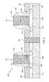
- FIG. 1a semiconductor structure 100 including an SOI substrate 102 is illustrated.
- the SOI substrate 102includes a bottom layer 104 , a BOX layer 106 and an SOI layer 108 .
- the SOI layer 108is an extremely thin SOI layer.
- the semiconductor structure 100may include a circuit including an NFET device 110 and a PFET device 112 .
- the NFET device 110includes source/drain extensions 114 formed in the SOI layer 108 .
- the NFET device 110has a gate structure 116 , spacers 118 and raised source/drain 120 .
- the PFET device 112includes source/drain extensions 122 formed in the SOI layer 108 , gate structure 124 , spacers 126 and raised source/drain 128 .
- the bottom layer 104may be implanted to form Well 1 130 and Well 2 132 which will form the back gate for NFET 110 and PFET 112 , respectively.
- NFET 110is formed so as to be located over Well 1 130 and PFET 112 is formed so as to be located over Well 2 132 .
- Well 1be a P-type well and Well 2 be an N-type well
- the implanted specie for the P well 130may be, for example, boron or boron fluoride (BF2) while the specie for the N well 132 may be, for example, arsenic or phosphorus.
- Well 1 130is an N-type well and Well 2 132 to be a P-type well so long as Well 1 130 and Well 2 132 are of opposite polarity.
- Separating the FET devices 110 , 112is shallow trench isolation (STI) 134 .
- STIshallow trench isolation
- a negative substrate bias 136(S x ⁇ 0) commensurate with the BOX layer thickness (enough to cause a change in the front-gate V T ) applied to the semiconductor structure 100 .
- a BOX layer thicknessof about 10 nanometers and a substrate bias of ⁇ 1V, there will be a change of approximately 180 mV in V T .
- the NFET source/drain extensions 114are “overlapped” with respect to the NFET gate structure 116 while the PFET source/drain extensions 122 are “underlapped” with respect to the PFET gate structure 124 .
- FIG. 2there is illustrated an enlarged cross sectional view of the first exemplary embodiment of FIG. 1 which better shows the overlapped condition of the NFET device 110 and the underlapped condition of the PFET device 112 .
- the gate structure 116has a gate edge 202 while the source/drain extensions 114 create a metallurgical junction 204 with the gate channel 208 .
- An overlapped conditionmay be defined as a structure where the metallurgical junction 204 extends into the gate channel 208 .
- the metallurgical junction 204may extend into the gate channel 208 by a distance shown as 206 , which for purposes of illustration and not limitation may be about 1 to 3 nanometers.
- the gate structure 124has a gate edge 214 while the source/drain extensions 122 create a metallurgical junction 210 with the gate channel 216 .
- An underlapped conditionmay be defined as a structure where the metallurgical junction 210 is spaced away from the gate edge 214 and away from the gate channel 216 .
- the metallurgical junction 210is spaced from the gate edge 214 and the gate channel 216 by a distance indicated by 212 .
- the distance 212will vary depending on the gate length but for purposes of illustration and not limitation, the distance 212 should be about 2 to 6 nanometers for a gate length of 25 nanometers.
- the NFET device 110has spacers 118 and PFET device 112 has spacers 126 .
- the PFET spacers 126may be enlarged to be bigger than the NFET spacers 118 .
- FIG. 3there is shown a second exemplary embodiment of the invention.
- the second exemplary embodimentis similar to the first exemplary embodiment except that the PFET device is now overlapped, while the NFET device is underlapped and the substrate bias is positive (S x >0).
- a semiconductor structure 300 including an SOI substrate 302is illustrated.
- the SOI substrate 302includes a bottom layer 304 , a BOX layer 306 and an SOI layer 308 .
- the SOI layer 308is an extremely thin SOI layer.
- the semiconductor structure 300may include a circuit including a PFET device 310 and an NFET device 312 .
- the PFET device 310includes source/drain extensions. 314 formed in the SOI layer 308 .
- the PFET device 310has a gate structure 316 , spacers 318 and raised source/drain 320 .
- the NFET device 312includes source/drain extensions 322 formed in the SOI layer 308 , gate structure 324 , spacers 326 and raised source/drain 328 .
- the bottom layer 304may be implanted to form Well 1 330 and Well 2 332 which will form the back gate for PFET 310 and NFET 312 , respectively.
- PFET 310is formed so as to be located over Well 1 330
- NFET 312is formed so as to be located over Well 2 332 .
- Well 1be an N-type well
- Well 2be a P-type well.
- the implanted specie for the N well 330may be, for example, arsenic or phosphorus while the specie for the P well 332 may be, for example, boron or boron fluoride (BF2).
- Well 1 330is a P-type well and Well 2 132 to be an N-type well so long as Well 1 330 and Well 2 332 are of opposite polarity.
- Separating the FET devices 310 , 312is shallow trench isolation (STI) 334 .
- STIshallow trench isolation
- a positive substrate bias 336commensurate with the BOX layer thickness (enough to cause a change in the front-gate V T ) applied to the semiconductor structure 300 .
- the BOX layer thicknessof about 10 nanometers and a substrate bias of +1V, there will be a change of approximately 150 mV in V T .
- the PFET source/drain extensions 314are “overlapped” with respect to the PFET gate structure 316 while the NFET source/drain extensions 322 are “underlapped” with respect to the NFET gate structure 324 .
- Overlapped and underlappedare as defined previously with respect to FIG. 2 .
- the semiconductor structure 100 in FIG. 1depicts an underlapped PFET device and an overlapped NFET device while the semiconductor structure 300 in FIG. 3 depicts an underlapped NFET device and an overlapped PFET device.
- the advantages of the exemplary embodimentsmay be achieved if only the PFET device is underlapped in FIG. 1 while the NFET device is not overlapped or underlapped.
- the advantages of the exemplary embodimentsalso may be achieved if only the NFET device is underlapped in FIG. 3 while the PFET device is not overlapped or underlapped.
- a negative substrate biasshould be applied when there is an underlapped PFET device as shown in FIG. 1 and a positive substrate bias should be applied when there is an underlapped NFET device as shown in FIG. 3 .
- the semiconductor structures 100 , 300may undergo additional conventional processing to form contacts and back end of the line wiring layers so as to form a semiconductor device such as a MOSFET. It is to be understood that the semiconductor structures shown in FIGS. 1 to 3 form only a part of a MOSFET and that there will be a plurality of such semiconductor structures in the finished MOSFET.
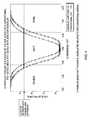
- FIG. 4shows the 1D junction profile at the center of the SOI layer for two simulated devices.
- One devicecorresponding to the first device in FIG. 5
- the second devicecorresponding to the third device in FIG. 5
- the underlap designshows a gate region approximately 7 nanometers wider than the conventional design.
- FIG. 5shows the device simulation results for these cases showing that the front-channel V T can be significantly reduced by applying negative substrate bias to PFET devices (comparing Rows 1 and 2).
- the V T reductioncomes with a degradation of DIBL and sub-threshold slope (Columns 6 and 7). The degradation in short-channel effects can be entirely recovered by using an underlapped PFET junction design whereby the V T reduction is maintained while the DIBL and sub-threshold slope are restored to conventional junction design (Row 3).
- the PFET device with negative substrate bias and underlapped junctionhas a lower V T than the conventional PFET device (Row 1) but without the degradation in DIBL and sub-threshold slope of the PFET device with negative substrate bias only (Row 2).
Landscapes
- Thin Film Transistor (AREA)
- Metal-Oxide And Bipolar Metal-Oxide Semiconductor Integrated Circuits (AREA)
Abstract
Description
Claims (23)
Priority Applications (1)
| Application Number | Priority Date | Filing Date | Title |
|---|---|---|---|
| US13/108,290US8598663B2 (en) | 2011-05-16 | 2011-05-16 | Semiconductor structure having NFET and PFET formed in SOI substrate with underlapped extensions |
Applications Claiming Priority (1)
| Application Number | Priority Date | Filing Date | Title |
|---|---|---|---|
| US13/108,290US8598663B2 (en) | 2011-05-16 | 2011-05-16 | Semiconductor structure having NFET and PFET formed in SOI substrate with underlapped extensions |
Publications (2)
| Publication Number | Publication Date |
|---|---|
| US20120292705A1 US20120292705A1 (en) | 2012-11-22 |
| US8598663B2true US8598663B2 (en) | 2013-12-03 |
Family
ID=47174316
Family Applications (1)
| Application Number | Title | Priority Date | Filing Date |
|---|---|---|---|
| US13/108,290Expired - Fee RelatedUS8598663B2 (en) | 2011-05-16 | 2011-05-16 | Semiconductor structure having NFET and PFET formed in SOI substrate with underlapped extensions |
Country Status (1)
| Country | Link |
|---|---|
| US (1) | US8598663B2 (en) |
Cited By (4)
| Publication number | Priority date | Publication date | Assignee | Title |
|---|---|---|---|---|
| US9390786B2 (en)* | 2014-08-13 | 2016-07-12 | Stmicroelectronics Sa | Method of minimizing the operating voltage of an SRAM cell |
| US9514997B2 (en) | 2015-03-25 | 2016-12-06 | International Business Machines Corporation | Silicon-germanium FinFET device with controlled junction |
| CN109427648A (en)* | 2017-08-31 | 2019-03-05 | 台湾积体电路制造股份有限公司 | Semiconductor device structure and forming method thereof |
| US10832939B2 (en) | 2018-04-11 | 2020-11-10 | Samsung Electronics Co., Ltd. | Semiconductor device and method of fabricating the same |
Families Citing this family (5)
| Publication number | Priority date | Publication date | Assignee | Title |
|---|---|---|---|---|
| WO2014162164A1 (en)* | 2013-04-03 | 2014-10-09 | Commissariat A L'energie Atomique Et Aux Eneriges Alternatives | Cmos in situ doped flow with independently tunable spacer thickness |
| US10049917B2 (en)* | 2016-09-19 | 2018-08-14 | Globalfoundries Inc. | FDSOI channel control by implanted high-K buried oxide |
| US9922973B1 (en)* | 2017-06-01 | 2018-03-20 | Globalfoundries Inc. | Switches with deep trench depletion and isolation structures |
| CN108807382B (en)* | 2018-06-14 | 2020-11-24 | 上海华力集成电路制造有限公司 | Semiconductor integrated circuits with HKMG |
| US12272299B1 (en)* | 2023-10-06 | 2025-04-08 | Globalfoundries U.S. Inc. | Compact memory-in-pixel display structure |
Citations (13)
| Publication number | Priority date | Publication date | Assignee | Title |
|---|---|---|---|---|
| US4577391A (en) | 1984-07-27 | 1986-03-25 | Monolithic Memories, Inc. | Method of manufacturing CMOS devices |
| US5461338A (en) | 1992-04-17 | 1995-10-24 | Nec Corporation | Semiconductor integrated circuit incorporated with substrate bias control circuit |
| US5838047A (en) | 1995-06-16 | 1998-11-17 | Mitsubishi Denki Kabushiki Kaisha | CMOS substrate biasing for threshold voltage control |
| US6198134B1 (en) | 1993-07-05 | 2001-03-06 | Mitsubishi Denki Kabushiki Kaisha | Semiconductor device having a common substrate bias |
| US6812527B2 (en) | 2002-09-05 | 2004-11-02 | International Business Machines Corporation | Method to control device threshold of SOI MOSFET's |
| US7259428B2 (en)* | 2004-08-05 | 2007-08-21 | Kabushiki Kaisha Toshiba | Semiconductor device using SOI structure having a triple-well region |
| US7342266B2 (en) | 2006-01-09 | 2008-03-11 | International Business Machines Corporation | Field effect transistors with dielectric source drain halo regions and reduced miller capacitance |
| US7479418B2 (en) | 2006-01-11 | 2009-01-20 | International Business Machines Corporation | Methods of applying substrate bias to SOI CMOS circuits |
| US20090065876A1 (en)* | 2007-09-10 | 2009-03-12 | Leland Chang | Metal High-K Transistor Having Silicon Sidewall for Reduced Parasitic Capacitance, and Process to Fabricate Same |
| US7638376B2 (en) | 2007-01-12 | 2009-12-29 | Taiwan Semiconductor Manufacturing Co., Ltd. | Method for forming SOI device |
| US20100038686A1 (en)* | 2008-08-14 | 2010-02-18 | Advanced Micro Devices, Inc. | Soi substrates and devices on soi substrates having a silicon nitride diffusion inhibition layer and methods for fabricating |
| US20100045364A1 (en) | 2008-08-25 | 2010-02-25 | Taiwan Semiconductor Manufacturing Company, Ltd. | Adaptive voltage bias methodology |
| US8119473B2 (en)* | 2009-12-31 | 2012-02-21 | Taiwan Semiconductor Manufacturing Company, Ltd. | High temperature anneal for aluminum surface protection |
- 2011
- 2011-05-16USUS13/108,290patent/US8598663B2/ennot_activeExpired - Fee Related
Patent Citations (13)
| Publication number | Priority date | Publication date | Assignee | Title |
|---|---|---|---|---|
| US4577391A (en) | 1984-07-27 | 1986-03-25 | Monolithic Memories, Inc. | Method of manufacturing CMOS devices |
| US5461338A (en) | 1992-04-17 | 1995-10-24 | Nec Corporation | Semiconductor integrated circuit incorporated with substrate bias control circuit |
| US6198134B1 (en) | 1993-07-05 | 2001-03-06 | Mitsubishi Denki Kabushiki Kaisha | Semiconductor device having a common substrate bias |
| US5838047A (en) | 1995-06-16 | 1998-11-17 | Mitsubishi Denki Kabushiki Kaisha | CMOS substrate biasing for threshold voltage control |
| US6812527B2 (en) | 2002-09-05 | 2004-11-02 | International Business Machines Corporation | Method to control device threshold of SOI MOSFET's |
| US7259428B2 (en)* | 2004-08-05 | 2007-08-21 | Kabushiki Kaisha Toshiba | Semiconductor device using SOI structure having a triple-well region |
| US7342266B2 (en) | 2006-01-09 | 2008-03-11 | International Business Machines Corporation | Field effect transistors with dielectric source drain halo regions and reduced miller capacitance |
| US7479418B2 (en) | 2006-01-11 | 2009-01-20 | International Business Machines Corporation | Methods of applying substrate bias to SOI CMOS circuits |
| US7638376B2 (en) | 2007-01-12 | 2009-12-29 | Taiwan Semiconductor Manufacturing Co., Ltd. | Method for forming SOI device |
| US20090065876A1 (en)* | 2007-09-10 | 2009-03-12 | Leland Chang | Metal High-K Transistor Having Silicon Sidewall for Reduced Parasitic Capacitance, and Process to Fabricate Same |
| US20100038686A1 (en)* | 2008-08-14 | 2010-02-18 | Advanced Micro Devices, Inc. | Soi substrates and devices on soi substrates having a silicon nitride diffusion inhibition layer and methods for fabricating |
| US20100045364A1 (en) | 2008-08-25 | 2010-02-25 | Taiwan Semiconductor Manufacturing Company, Ltd. | Adaptive voltage bias methodology |
| US8119473B2 (en)* | 2009-12-31 | 2012-02-21 | Taiwan Semiconductor Manufacturing Company, Ltd. | High temperature anneal for aluminum surface protection |
Non-Patent Citations (1)
| Title |
|---|
| A. Bansal et al., "Optimal Dual-Vt design in Sub-100-nm PD/SOI and Double-Gate Technologies," IEEE Transactions on Electron Devices, vol. 55, No. 5, May 2008, pp. 1161-1169. |
Cited By (6)
| Publication number | Priority date | Publication date | Assignee | Title |
|---|---|---|---|---|
| US9390786B2 (en)* | 2014-08-13 | 2016-07-12 | Stmicroelectronics Sa | Method of minimizing the operating voltage of an SRAM cell |
| US9514997B2 (en) | 2015-03-25 | 2016-12-06 | International Business Machines Corporation | Silicon-germanium FinFET device with controlled junction |
| US9922886B2 (en) | 2015-03-25 | 2018-03-20 | International Business Machines Corporation | Silicon-germanium FinFET device with controlled junction |
| CN109427648A (en)* | 2017-08-31 | 2019-03-05 | 台湾积体电路制造股份有限公司 | Semiconductor device structure and forming method thereof |
| CN109427648B (en)* | 2017-08-31 | 2020-11-03 | 台湾积体电路制造股份有限公司 | Semiconductor device structure and forming method thereof |
| US10832939B2 (en) | 2018-04-11 | 2020-11-10 | Samsung Electronics Co., Ltd. | Semiconductor device and method of fabricating the same |
Also Published As
| Publication number | Publication date |
|---|---|
| US20120292705A1 (en) | 2012-11-22 |
Similar Documents
| Publication | Publication Date | Title |
|---|---|---|
| US8598663B2 (en) | Semiconductor structure having NFET and PFET formed in SOI substrate with underlapped extensions | |
| CN111668288B (en) | Heavily doped buried layer to reduce MOSFET off capacitance | |
| US9793408B2 (en) | Fin field effect transistor (FinFET) | |
| US8546228B2 (en) | Strained thin body CMOS device having vertically raised source/drain stressors with single spacer | |
| US6380590B1 (en) | SOI chip having multiple threshold voltage MOSFETs by using multiple channel materials and method of fabricating same | |
| US9768074B2 (en) | Transistor structure and fabrication methods with an epitaxial layer over multiple halo implants | |
| US7494850B2 (en) | Ultra-thin logic and backgated ultra-thin SRAM | |
| US20090302388A1 (en) | Method for Fabricating Super-Steep Retrograde Well Mosfet on SOI or Bulk Silicon Substrate, and Device Fabricated in Accordance with the Method | |
| US20140319624A1 (en) | Methods of forming a finfet semiconductor device by performing an epitaxial growth process | |
| US8748986B1 (en) | Electronic device with controlled threshold voltage | |
| US20140015067A1 (en) | Source/drain extension control for advanced transistors | |
| US11183591B2 (en) | Lateral double-diffused metal-oxide-semiconductor (LDMOS) fin field effect transistor with enhanced capabilities | |
| KR20020062200A (en) | Semiconductor device and method of fabricating the same | |
| JP2014038898A (en) | Semiconductor device | |
| JP2015056619A (en) | Semiconductor device | |
| EP1135805A1 (en) | Insulated channel field effect transistor with an electric field terminal region | |
| US10777558B1 (en) | CMOS-based integrated circuit products with isolated P-wells for body-biasing transistor devices | |
| US7795083B2 (en) | Semiconductor structure and fabrication method thereof | |
| US20090170269A1 (en) | High voltage mosfet devices containing tip compensation implant | |
| US9536880B2 (en) | Devices having multiple threshold voltages and method of fabricating such devices | |
| US11488871B2 (en) | Transistor structure with multiple halo implants having epitaxial layer over semiconductor-on-insulator substrate | |
| US9184179B2 (en) | Thin channel-on-insulator MOSFET device with n+ epitaxy substrate and embedded stressor | |
| US11398555B2 (en) | Transistor device with a plurality of active gates that can be individually modulated to change performance characteristics of the transistor | |
| JP2018107230A (en) | Semiconductor device and manufacturing method thereof | |
| Saramekala | Modeling and simulation of subthreshold characteristics of short-channel fully-depleted recessed-source/Drain SOI MOSFETs |
Legal Events
| Date | Code | Title | Description |
|---|---|---|---|
| AS | Assignment | Owner name:INTERNATIONAL BUSINESS MACHINES CORPORATION, NEW Y Free format text:ASSIGNMENT OF ASSIGNORS INTEREST;ASSIGNORS:CHENG, KANGGUO;DORIS, BRUCE B.;HARAN, BALASUBRAMANIAN S.;AND OTHERS;SIGNING DATES FROM 20110511 TO 20110513;REEL/FRAME:026283/0010 | |
| AS | Assignment | Owner name:GLOBALFOUNDRIES U.S. 2 LLC, NEW YORK Free format text:ASSIGNMENT OF ASSIGNORS INTEREST;ASSIGNOR:INTERNATIONAL BUSINESS MACHINES CORPORATION;REEL/FRAME:036550/0001 Effective date:20150629 | |
| AS | Assignment | Owner name:GLOBALFOUNDRIES INC., CAYMAN ISLANDS Free format text:ASSIGNMENT OF ASSIGNORS INTEREST;ASSIGNORS:GLOBALFOUNDRIES U.S. 2 LLC;GLOBALFOUNDRIES U.S. INC.;REEL/FRAME:036779/0001 Effective date:20150910 | |
| REMI | Maintenance fee reminder mailed | ||
| LAPS | Lapse for failure to pay maintenance fees | Free format text:PATENT EXPIRED FOR FAILURE TO PAY MAINTENANCE FEES (ORIGINAL EVENT CODE: EXP.) | |
| STCH | Information on status: patent discontinuation | Free format text:PATENT EXPIRED DUE TO NONPAYMENT OF MAINTENANCE FEES UNDER 37 CFR 1.362 | |
| FP | Lapsed due to failure to pay maintenance fee | Effective date:20171203 | |
| AS | Assignment | Owner name:GLOBALFOUNDRIES U.S. INC., NEW YORK Free format text:RELEASE BY SECURED PARTY;ASSIGNOR:WILMINGTON TRUST, NATIONAL ASSOCIATION;REEL/FRAME:056987/0001 Effective date:20201117 |