US8598633B2 - Semiconductor device having contact layer providing electrical connections - Google Patents
Semiconductor device having contact layer providing electrical connectionsDownload PDFInfo
- Publication number
- US8598633B2 US8598633B2US13/351,101US201213351101AUS8598633B2US 8598633 B2US8598633 B2US 8598633B2US 201213351101 AUS201213351101 AUS 201213351101AUS 8598633 B2US8598633 B2US 8598633B2
- Authority
- US
- United States
- Prior art keywords
- length
- contact layer
- diffusion region
- semiconductor device
- set forth
- Prior art date
- Legal status (The legal status is an assumption and is not a legal conclusion. Google has not performed a legal analysis and makes no representation as to the accuracy of the status listed.)
- Active
Links
Images


Classifications
- H—ELECTRICITY
- H01—ELECTRIC ELEMENTS
- H01L—SEMICONDUCTOR DEVICES NOT COVERED BY CLASS H10
- H01L21/00—Processes or apparatus adapted for the manufacture or treatment of semiconductor or solid state devices or of parts thereof
- H01L21/70—Manufacture or treatment of devices consisting of a plurality of solid state components formed in or on a common substrate or of parts thereof; Manufacture of integrated circuit devices or of parts thereof
- H01L21/71—Manufacture of specific parts of devices defined in group H01L21/70
- H01L21/768—Applying interconnections to be used for carrying current between separate components within a device comprising conductors and dielectrics
- H01L21/76838—Applying interconnections to be used for carrying current between separate components within a device comprising conductors and dielectrics characterised by the formation and the after-treatment of the conductors
- H01L21/76895—Local interconnects; Local pads, as exemplified by patent document EP0896365
- H—ELECTRICITY
- H01—ELECTRIC ELEMENTS
- H01L—SEMICONDUCTOR DEVICES NOT COVERED BY CLASS H10
- H01L21/00—Processes or apparatus adapted for the manufacture or treatment of semiconductor or solid state devices or of parts thereof
- H01L21/70—Manufacture or treatment of devices consisting of a plurality of solid state components formed in or on a common substrate or of parts thereof; Manufacture of integrated circuit devices or of parts thereof
- H01L21/71—Manufacture of specific parts of devices defined in group H01L21/70
- H01L21/768—Applying interconnections to be used for carrying current between separate components within a device comprising conductors and dielectrics
- H01L21/76897—Formation of self-aligned vias or contact plugs, i.e. involving a lithographically uncritical step
- H—ELECTRICITY
- H01—ELECTRIC ELEMENTS
- H01L—SEMICONDUCTOR DEVICES NOT COVERED BY CLASS H10
- H01L23/00—Details of semiconductor or other solid state devices
- H01L23/52—Arrangements for conducting electric current within the device in operation from one component to another, i.e. interconnections, e.g. wires, lead frames
- H01L23/522—Arrangements for conducting electric current within the device in operation from one component to another, i.e. interconnections, e.g. wires, lead frames including external interconnections consisting of a multilayer structure of conductive and insulating layers inseparably formed on the semiconductor body
- H01L23/528—Layout of the interconnection structure
- H01L23/5286—Arrangements of power or ground buses
- H—ELECTRICITY
- H10—SEMICONDUCTOR DEVICES; ELECTRIC SOLID-STATE DEVICES NOT OTHERWISE PROVIDED FOR
- H10D—INORGANIC ELECTRIC SEMICONDUCTOR DEVICES
- H10D84/00—Integrated devices formed in or on semiconductor substrates that comprise only semiconducting layers, e.g. on Si wafers or on GaAs-on-Si wafers
- H10D84/01—Manufacture or treatment
- H10D84/0123—Integrating together multiple components covered by H10D12/00 or H10D30/00, e.g. integrating multiple IGBTs
- H10D84/0126—Integrating together multiple components covered by H10D12/00 or H10D30/00, e.g. integrating multiple IGBTs the components including insulated gates, e.g. IGFETs
- H10D84/0149—Manufacturing their interconnections or electrodes, e.g. source or drain electrodes
- H—ELECTRICITY
- H10—SEMICONDUCTOR DEVICES; ELECTRIC SOLID-STATE DEVICES NOT OTHERWISE PROVIDED FOR
- H10D—INORGANIC ELECTRIC SEMICONDUCTOR DEVICES
- H10D84/00—Integrated devices formed in or on semiconductor substrates that comprise only semiconducting layers, e.g. on Si wafers or on GaAs-on-Si wafers
- H10D84/80—Integrated devices formed in or on semiconductor substrates that comprise only semiconducting layers, e.g. on Si wafers or on GaAs-on-Si wafers characterised by the integration of at least one component covered by groups H10D12/00 or H10D30/00, e.g. integration of IGFETs
- H10D84/82—Integrated devices formed in or on semiconductor substrates that comprise only semiconducting layers, e.g. on Si wafers or on GaAs-on-Si wafers characterised by the integration of at least one component covered by groups H10D12/00 or H10D30/00, e.g. integration of IGFETs of only field-effect components
- H10D84/83—Integrated devices formed in or on semiconductor substrates that comprise only semiconducting layers, e.g. on Si wafers or on GaAs-on-Si wafers characterised by the integration of at least one component covered by groups H10D12/00 or H10D30/00, e.g. integration of IGFETs of only field-effect components of only insulated-gate FETs [IGFET]
- H—ELECTRICITY
- H01—ELECTRIC ELEMENTS
- H01L—SEMICONDUCTOR DEVICES NOT COVERED BY CLASS H10
- H01L2924/00—Indexing scheme for arrangements or methods for connecting or disconnecting semiconductor or solid-state bodies as covered by H01L24/00
- H01L2924/0001—Technical content checked by a classifier
- H01L2924/0002—Not covered by any one of groups H01L24/00, H01L24/00 and H01L2224/00
- H—ELECTRICITY
- H10—SEMICONDUCTOR DEVICES; ELECTRIC SOLID-STATE DEVICES NOT OTHERWISE PROVIDED FOR
- H10D—INORGANIC ELECTRIC SEMICONDUCTOR DEVICES
- H10D84/00—Integrated devices formed in or on semiconductor substrates that comprise only semiconducting layers, e.g. on Si wafers or on GaAs-on-Si wafers
- H10D84/01—Manufacture or treatment
- H10D84/02—Manufacture or treatment characterised by using material-based technologies
- H10D84/03—Manufacture or treatment characterised by using material-based technologies using Group IV technology, e.g. silicon technology or silicon-carbide [SiC] technology
- H10D84/038—Manufacture or treatment characterised by using material-based technologies using Group IV technology, e.g. silicon technology or silicon-carbide [SiC] technology using silicon technology, e.g. SiGe
Definitions
- the present inventiongenerally relates to a semiconductor device, and more particularly relates to power connections to transistors in semiconductor devices
- typical semiconductor devices 100include a plurality of transistors 102 formed within a diffusion region 104 .
- the semiconductor devices 100utilize power rails 106 , as part of a first metal layer 107 , to deliver a reference voltage and/or ground to the transistors 102 .
- the power rail 106includes power tabs 108 that extend into the diffusion region 104 .
- a via 110then electrically connects the power tab 108 to a source (not shown) or a drain (not shown) of one of the transistors 102 .
- the projection of the power tabs 108 into the diffusion region 104causes difficulties, as the metal layer 107 is also routinely utilized for local interconnection between the transistors 102 and as cell pins 112 . This leads to a very complicated patterning for the first metal layer 107 , as is shown in FIG. 2 , which routinely leads to fabrication difficulties and/or compromises in standard cell design.
- One solutionis to use a second metal layer (not shown) on a different plane from the first metal layer 107 .
- the use of the second metal layerreduces routing efficiency and results in a larger and more expensive implementation of the semiconductor device 100 .
- a semiconductor deviceincludes a semiconductor substrate having a diffusion region.
- a transistoris formed within the diffusion region.
- the transistorincludes a source, a drain, and a gate.
- a power railis disposed outside the diffusion region.
- the devicefurther includes a contact layer disposed above the substrate and below the power rail.
- a viais disposed between the contact layer and the power rail to electrically connect the contact layer to the power rail.
- the contact layerincludes a first length disposed outside the diffusion region and a second length extending from the first length into the diffusion region and electrically connected to the transistor.
- FIG. 1is a top view of a portion of a semiconductor device according to the prior art showing power tabs extending from power rails into a diffusion region;
- FIG. 2is a top view of a metal layer of a semiconductor device according to the prior art including the power tabs and power rails;
- FIG. 3is a top view of a semiconductor device according to the present invention.
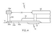
- FIG. 4is a side view of a portion of the semiconductor device according to the present invention as viewed along a line 4 - 4 shown in FIG. 3 ;
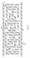
- FIG. 5is a top view of a metal layer of a semiconductor device according to the present invention.
- a semiconductor device 10is shown and described herein.
- the semiconductor device 10may be part of an integrated circuit (not separately numbered) as is well recognized by those skilled in the art.
- the semiconductor device 10includes a semiconductor substrate 12 .
- the semiconductor substrate 12includes at least one diffusion region 14 and at least one transistor 16 formed in the at least one diffusion region 14 .
- a first diffusion region 14 a and a second diffusion region 14 bare shown with a plurality of transistors 16 formed in each region 14 a , 14 b .
- additional diffusion regions 14 a , 14 bmay be implemented.
- the transistors 16are field-effect transistors (FETs) and more specifically, metal-oxide-semiconductor field-effect transistors (MOSFETs). Each of the transistors 16 includes a source 18 , a drain 20 , and a gate 22 .
- the sources 18 , drains 20 , and gates 22are formed in and/or on the substrate 12 using techniques that are well known to those skilled in the art.
- the gates 22are formed primarily of polycrystalline silicon, commonly referred to as polysilicon or simply PolySi, disposed above the substrate 12 .
- the gates 22are formed as strips 24 generally parallel to one another.
- the strips 24are generally linear in shape as is appreciated by those skilled in the art.
- Gapsmay be formed in the strips 24 such that more than one transistor 16 may be disposed along each strip 24 . Such gaps may be formed using cut mask techniques as readily appreciated by those skilled in the art.
- the semiconductor device 10includes at least one metal layer 25 disposed above the substrate 12 .
- the at least one metal layer 25is also disposed above the sources 18 , drains 20 , and gates 22 , of the transistors 16 .
- the at least one metal layer 25is formed of copper or some other electrically conductive metal as realized by those skilled in the art.
- Metal layers 25are routinely labeled and referred to as Metal 1 , Metal 2 , etc. or M 1 , M 2 , etc., as is appreciated by those skilled in the art.
- the metal layer 25 of the illustrated embodimentincludes at least one power rail 26 .
- the power rail 26typically provides a reference voltage or ground as is appreciated by those skilled in the art.
- the at least one power rail 26is disposed outside the at least one diffusion region 14 . That is, the at least one power rail 26 does not overlap the at least one diffusion region 14 . Said another way, the at least one power rail 26 does not extend into, over, or under the at least one diffusion region 14 .
- a first power rail 26 ais disposed outside and adjacent to the first diffusion region 14 a .
- a second power rail 26 bis disposed outside and adjacent to the second diffusion region 14 b.
- each power rail 26 a , 26 bis generally linear in shape. That is, at least a section of each power rail 26 a , 26 b extends longitudinally, i.e., along a length. Particularly, the section of each power rail 26 a , 26 b is generally linear adjacent to the respective diffusion region 14 a , 14 b .
- the at least one power rail 26may include additional curves, bends, or other non-linear sections.
- the semiconductor device 10further includes at least one contact layer 28 for providing electrical connections between the at least one power rail 26 and the at least one transistor 16 .
- the at least one contact layer 28is formed of a semiconductor material, e.g., silicon. However, the at least one contact layer 28 may be formed of other semiconductor materials or other suitable materials to provide electrical conductivity as realized by those skilled in the art.
- the at least one contact layer 28is disposed above the substrate 12 and below the at least one power rail 26 . Said another way, the at least one contact layer 28 is sandwiched between the substrate 12 and the at least one power rail 26 . More specifically, in the illustrated embodiments, at least a portion of the at least one contact layer 28 is disposed directly on the substrate 12 , as is shown in FIG. 4 .
- the semiconductor device 10 of the illustrated embodimentincludes a first contact layer 28 a and a second contact layer 28 b.
- the at least one contact layer 28includes at least a first length 30 and a second length 32 .
- the first length 30 of the at least one contact layer 28is disposed outside the at least one diffusion region 14 . That is, the first length 30 of the at least one contact layer 28 does not overlap the at least one diffusion region 14 .
- each contact layer 28 a , 28 bincludes a first length 30 a , 30 b that runs generally congruent with the respective power rail 26 a , 26 b . That is, the first length 30 a , 30 b of each contact layer 28 a , 28 b is disposed directly below the respective power rail 26 a , 26 b .
- the first length 30 a , 30 b of each contact layer 28 a , 28 bis also generally linear in shape. Furthermore, in the illustrated embodiment, the first length 30 a , 30 b of each contact layer 28 a , 28 b is generally perpendicular to the gates 22 of the transistors 16 .
- At least one via 36is disposed between the at least one contact layer 28 and the at least one power rail 26 .
- the at least one via 36electrically connects the at least one contact layer 28 to the at least one power rail 26 .
- a plurality of vias 36are disposed between each power rail 26 a , 26 b and the first length 30 a , 30 b of each contact layer 28 a , 28 b .
- the vias 36 of the illustrated embodimentare spaced from one another to provide balanced electrical conductivity between the contact layers 28 a , 28 b and the power rails 26 a , 26 b.
- the at least one contact layer 28includes at least one additional length 32 , 34 extending from the first length 30 into the at least one diffusion region 14 .
- Each additional length 32 , 34is electrically connected to at least one of the transistors 16 .
- each additional length 32 , 34is electrically connected to a source 18 or a drain 20 of a transistor.
- at least one of the additional lengths 32 , 34may be electrically connected to the gate 22 of one of the transistors 16 .
- Each contact layer 28 a , 28 b of the illustrated embodimentincludes a second length, 32 a , 32 b and a third length 34 a , 34 b .
- the second and third lengths 32 a , 32 b , 34 a , 34 b of the contact layers 28 a , 28 bare also generally linear in shape.
- the second and third lengths 32 a , 32 b , 34 a , 34 bare each generally perpendicular to the respective first lengths 30 a , 30 b of the contact layers 28 a , 28 b .
- the second and third lengths 32 a , 32 b , 34 a , 34 bare each generally parallel to the gates 22 of the transistors 16 .
- the metal layer 25can be more simply and succinctly utilized for interconnections between the transistors 16 , as is shown in FIG. 5 .
- the metal layer 25 of the semiconductor device 10may also include a pin layer 38 positioned above the at least one transistor 16 .
- the pin layer 38is a standard feature of Complementary metal-oxide-semiconductor (“CMOS”) circuits.
- CMOSComplementary metal-oxide-semiconductor
- the pin layer 38is typically used to connected the source or drain of a p-channel transistor to a source or drain of an n-channel transistor.
- the pin layer 38extends from the diffusion region 14 to outside of the diffusion region 14 . More specifically, the pin layer 38 of the illustrated embodiment extends between the first diffusion region 14 a and the second diffusion region 14 b.
- the pin layer 38can be sized larger, i.e., have a greater length, width, and/or surface area, when compared to prior art devices, as there is no projection of the metal layer 25 from the power rail 26 into the diffusion region 14 . This will improve conductivity between the pin layer 38 and other components (not shown).
Landscapes
- Engineering & Computer Science (AREA)
- Physics & Mathematics (AREA)
- Microelectronics & Electronic Packaging (AREA)
- General Physics & Mathematics (AREA)
- Computer Hardware Design (AREA)
- Condensed Matter Physics & Semiconductors (AREA)
- Power Engineering (AREA)
- Manufacturing & Machinery (AREA)
- Geometry (AREA)
- Insulated Gate Type Field-Effect Transistor (AREA)
- Metal-Oxide And Bipolar Metal-Oxide Semiconductor Integrated Circuits (AREA)
- Design And Manufacture Of Integrated Circuits (AREA)
- Electrodes Of Semiconductors (AREA)
- Semiconductor Integrated Circuits (AREA)
- Thin Film Transistor (AREA)
Abstract
Description
Claims (19)
Priority Applications (6)
| Application Number | Priority Date | Filing Date | Title |
|---|---|---|---|
| US13/351,101US8598633B2 (en) | 2012-01-16 | 2012-01-16 | Semiconductor device having contact layer providing electrical connections |
| TW101127702ATWI499036B (en) | 2012-01-16 | 2012-08-01 | Semiconductor equipment |
| SG2012058699ASG192321A1 (en) | 2012-01-16 | 2012-08-06 | Semiconductor device |
| DE102012215529.5ADE102012215529B4 (en) | 2012-01-16 | 2012-08-31 | Semiconductor device |
| KR1020120109238AKR101616490B1 (en) | 2012-01-16 | 2012-09-28 | Semiconductor device |
| CN201310013910.9ACN103208493B (en) | 2012-01-16 | 2013-01-15 | Semiconductor equipment |
Applications Claiming Priority (1)
| Application Number | Priority Date | Filing Date | Title |
|---|---|---|---|
| US13/351,101US8598633B2 (en) | 2012-01-16 | 2012-01-16 | Semiconductor device having contact layer providing electrical connections |
Publications (2)
| Publication Number | Publication Date |
|---|---|
| US20130181289A1 US20130181289A1 (en) | 2013-07-18 |
| US8598633B2true US8598633B2 (en) | 2013-12-03 |
Family
ID=48693287
Family Applications (1)
| Application Number | Title | Priority Date | Filing Date |
|---|---|---|---|
| US13/351,101ActiveUS8598633B2 (en) | 2012-01-16 | 2012-01-16 | Semiconductor device having contact layer providing electrical connections |
Country Status (6)
| Country | Link |
|---|---|
| US (1) | US8598633B2 (en) |
| KR (1) | KR101616490B1 (en) |
| CN (1) | CN103208493B (en) |
| DE (1) | DE102012215529B4 (en) |
| SG (1) | SG192321A1 (en) |
| TW (1) | TWI499036B (en) |
Cited By (2)
| Publication number | Priority date | Publication date | Assignee | Title |
|---|---|---|---|---|
| US9496179B2 (en) | 2014-08-25 | 2016-11-15 | Samsung Electronics Co., Ltd. | Method of manufacturing semiconductor devices |
| US10811357B2 (en) | 2017-04-11 | 2020-10-20 | Samsung Electronics Co., Ltd. | Standard cell and an integrated circuit including the same |
Families Citing this family (1)
| Publication number | Priority date | Publication date | Assignee | Title |
|---|---|---|---|---|
| US9691750B2 (en)* | 2015-01-30 | 2017-06-27 | Taiwan Semiconductor Manufacturing Company Ltd. | Semiconductor device and layout method thereof |
Citations (3)
| Publication number | Priority date | Publication date | Assignee | Title |
|---|---|---|---|---|
| JP2005183681A (en) | 2003-12-19 | 2005-07-07 | Sony Corp | Semiconductor integrated circuit |
| US20090108360A1 (en)* | 2007-10-26 | 2009-04-30 | Tela Innovations, Inc. | Methods, structures and designs for self-aligning local interconnects used in integrated circuits |
| US20110235407A1 (en)* | 2010-03-24 | 2011-09-29 | Sun-Me Lim | Semiconductor memory device and a method of manufacturing the same |
Family Cites Families (5)
| Publication number | Priority date | Publication date | Assignee | Title |
|---|---|---|---|---|
| JP4685388B2 (en)* | 2004-09-06 | 2011-05-18 | Okiセミコンダクタ株式会社 | Semiconductor device |
| US20060145263A1 (en)* | 2005-01-06 | 2006-07-06 | Macronix International Co., Ltd. | Plasma damage protection circuit for protecting multiple word lines or strapped word lines of a memory device |
| JP2008112934A (en)* | 2006-10-31 | 2008-05-15 | Oki Electric Ind Co Ltd | Semiconductor memory, and its manufacturing method |
| JP5130596B2 (en)* | 2007-05-30 | 2013-01-30 | 国立大学法人東北大学 | Semiconductor device |
| US20100052896A1 (en)* | 2008-09-02 | 2010-03-04 | Jesse Bruce Goodman | Fall detection system and method |
- 2012
- 2012-01-16USUS13/351,101patent/US8598633B2/enactiveActive
- 2012-08-01TWTW101127702Apatent/TWI499036B/enactive
- 2012-08-06SGSG2012058699Apatent/SG192321A1/enunknown
- 2012-08-31DEDE102012215529.5Apatent/DE102012215529B4/enactiveActive
- 2012-09-28KRKR1020120109238Apatent/KR101616490B1/enactiveActive
- 2013
- 2013-01-15CNCN201310013910.9Apatent/CN103208493B/enactiveActive
Patent Citations (7)
| Publication number | Priority date | Publication date | Assignee | Title |
|---|---|---|---|---|
| JP2005183681A (en) | 2003-12-19 | 2005-07-07 | Sony Corp | Semiconductor integrated circuit |
| US20090108360A1 (en)* | 2007-10-26 | 2009-04-30 | Tela Innovations, Inc. | Methods, structures and designs for self-aligning local interconnects used in integrated circuits |
| US7763534B2 (en)* | 2007-10-26 | 2010-07-27 | Tela Innovations, Inc. | Methods, structures and designs for self-aligning local interconnects used in integrated circuits |
| US20100252896A1 (en)* | 2007-10-26 | 2010-10-07 | Tela Innovations, Inc. | Methods, Structures, and Designs for Self-Aligning Local Interconnects used in Integrated Circuits |
| US7994545B2 (en)* | 2007-10-26 | 2011-08-09 | Tela Innovations, Inc. | Methods, structures, and designs for self-aligning local interconnects used in integrated circuits |
| US20110278681A1 (en) | 2007-10-26 | 2011-11-17 | Tela Innovations, Inc. | Methods, Structures, and Designs for Self-Aligning Local Interconnects used in Integrated Circuits |
| US20110235407A1 (en)* | 2010-03-24 | 2011-09-29 | Sun-Me Lim | Semiconductor memory device and a method of manufacturing the same |
Non-Patent Citations (1)
| Title |
|---|
| English translation of German Office Action prepared by German Patent office on Nov. 30, 2012 for DE 10 2012 215 529.5. |
Cited By (3)
| Publication number | Priority date | Publication date | Assignee | Title |
|---|---|---|---|---|
| US9496179B2 (en) | 2014-08-25 | 2016-11-15 | Samsung Electronics Co., Ltd. | Method of manufacturing semiconductor devices |
| US10811357B2 (en) | 2017-04-11 | 2020-10-20 | Samsung Electronics Co., Ltd. | Standard cell and an integrated circuit including the same |
| US12125787B2 (en) | 2017-04-11 | 2024-10-22 | Samsung Electronics Co., Ltd. | Standard cell and an integrated circuit including the same |
Also Published As
| Publication number | Publication date |
|---|---|
| KR101616490B1 (en) | 2016-04-28 |
| KR20130084205A (en) | 2013-07-24 |
| DE102012215529A1 (en) | 2013-07-18 |
| CN103208493A (en) | 2013-07-17 |
| US20130181289A1 (en) | 2013-07-18 |
| DE102012215529B4 (en) | 2018-07-12 |
| CN103208493B (en) | 2015-09-23 |
| TWI499036B (en) | 2015-09-01 |
| SG192321A1 (en) | 2013-08-30 |
| TW201332086A (en) | 2013-08-01 |
Similar Documents
| Publication | Publication Date | Title |
|---|---|---|
| US12148702B2 (en) | Semiconductor device with transistor local interconnects | |
| US8581348B2 (en) | Semiconductor device with transistor local interconnects | |
| US9935100B2 (en) | Power rail inbound middle of line (MOL) routing | |
| CN104425443A (en) | Semiconductor logic circuits fabricated using multi-layer structures | |
| US8859416B2 (en) | Software and method for via spacing in a semiconductor device | |
| US9634026B1 (en) | Standard cell architecture for reduced leakage current and improved decoupling capacitance | |
| US20170229457A1 (en) | Semiconductor integrated circuit | |
| US20170317082A1 (en) | Field effect transistor structure for reducing contact resistance | |
| US20180145070A1 (en) | Electromigration Resistant Semiconductor Device | |
| US9450089B2 (en) | Semiconductor device | |
| US8598633B2 (en) | Semiconductor device having contact layer providing electrical connections | |
| US7002210B2 (en) | Semiconductor device including a high-breakdown voltage MOS transistor | |
| KR101858545B1 (en) | Gate rounding for reduced transistor leakage current | |
| US9960231B2 (en) | Standard cell architecture for parasitic resistance reduction | |
| US20140264585A1 (en) | Semiconductor device including lateral double diffused metal oxide semiconductor | |
| US10692808B2 (en) | High performance cell design in a technology with high density metal routing | |
| CN203910810U (en) | Metal-oxide-semiconductor field effect transistor |
Legal Events
| Date | Code | Title | Description |
|---|---|---|---|
| AS | Assignment | Owner name:GLOBALFOUNDRIES INC., CAYMAN ISLANDS Free format text:ASSIGNMENT OF ASSIGNORS INTEREST;ASSIGNORS:TARABBIA, MARC;GULLETTE, JAMES B.;RASHED, MAHBUB;AND OTHERS;SIGNING DATES FROM 20111105 TO 20120123;REEL/FRAME:027580/0817 | |
| STCF | Information on status: patent grant | Free format text:PATENTED CASE | |
| FPAY | Fee payment | Year of fee payment:4 | |
| AS | Assignment | Owner name:WILMINGTON TRUST, NATIONAL ASSOCIATION, DELAWARE Free format text:SECURITY AGREEMENT;ASSIGNOR:GLOBALFOUNDRIES INC.;REEL/FRAME:049490/0001 Effective date:20181127 | |
| AS | Assignment | Owner name:GLOBALFOUNDRIES U.S. INC., CALIFORNIA Free format text:ASSIGNMENT OF ASSIGNORS INTEREST;ASSIGNOR:GLOBALFOUNDRIES INC.;REEL/FRAME:050122/0001 Effective date:20190821 | |
| AS | Assignment | Owner name:GLOBALFOUNDRIES INC., CAYMAN ISLANDS Free format text:RELEASE BY SECURED PARTY;ASSIGNOR:WILMINGTON TRUST, NATIONAL ASSOCIATION;REEL/FRAME:054636/0001 Effective date:20201117 | |
| MAFP | Maintenance fee payment | Free format text:PAYMENT OF MAINTENANCE FEE, 8TH YEAR, LARGE ENTITY (ORIGINAL EVENT CODE: M1552); ENTITY STATUS OF PATENT OWNER: LARGE ENTITY Year of fee payment:8 | |
| MAFP | Maintenance fee payment | Free format text:PAYMENT OF MAINTENANCE FEE, 12TH YEAR, LARGE ENTITY (ORIGINAL EVENT CODE: M1553); ENTITY STATUS OF PATENT OWNER: LARGE ENTITY Year of fee payment:12 |