US8598606B2 - Solid metal block semiconductor light emitting device mounting substrates and packages - Google Patents
Solid metal block semiconductor light emitting device mounting substrates and packagesDownload PDFInfo
- Publication number
- US8598606B2 US8598606B2US12/363,000US36300009AUS8598606B2US 8598606 B2US8598606 B2US 8598606B2US 36300009 AUS36300009 AUS 36300009AUS 8598606 B2US8598606 B2US 8598606B2
- Authority
- US
- United States
- Prior art keywords
- light emitting
- semiconductor light
- emitting device
- mounting substrate
- flexible film
- Prior art date
- Legal status (The legal status is an assumption and is not a legal conclusion. Google has not performed a legal analysis and makes no representation as to the accuracy of the status listed.)
- Active, expires
Links
Images


Classifications
- H—ELECTRICITY
- H10—SEMICONDUCTOR DEVICES; ELECTRIC SOLID-STATE DEVICES NOT OTHERWISE PROVIDED FOR
- H10H—INORGANIC LIGHT-EMITTING SEMICONDUCTOR DEVICES HAVING POTENTIAL BARRIERS
- H10H20/00—Individual inorganic light-emitting semiconductor devices having potential barriers, e.g. light-emitting diodes [LED]
- H10H20/80—Constructional details
- H10H20/85—Packages
- H10H20/858—Means for heat extraction or cooling
- H10H20/8582—Means for heat extraction or cooling characterised by their shape
- F—MECHANICAL ENGINEERING; LIGHTING; HEATING; WEAPONS; BLASTING
- F21—LIGHTING
- F21V—FUNCTIONAL FEATURES OR DETAILS OF LIGHTING DEVICES OR SYSTEMS THEREOF; STRUCTURAL COMBINATIONS OF LIGHTING DEVICES WITH OTHER ARTICLES, NOT OTHERWISE PROVIDED FOR
- F21V29/00—Protecting lighting devices from thermal damage; Cooling or heating arrangements specially adapted for lighting devices or systems
- F21V29/50—Cooling arrangements
- F21V29/70—Cooling arrangements characterised by passive heat-dissipating elements, e.g. heat-sinks
- F21V29/74—Cooling arrangements characterised by passive heat-dissipating elements, e.g. heat-sinks with fins or blades
- F21V29/76—Cooling arrangements characterised by passive heat-dissipating elements, e.g. heat-sinks with fins or blades with essentially identical parallel planar fins or blades, e.g. with comb-like cross-section
- F21V29/763—Cooling arrangements characterised by passive heat-dissipating elements, e.g. heat-sinks with fins or blades with essentially identical parallel planar fins or blades, e.g. with comb-like cross-section the planes containing the fins or blades having the direction of the light emitting axis
- H—ELECTRICITY
- H10—SEMICONDUCTOR DEVICES; ELECTRIC SOLID-STATE DEVICES NOT OTHERWISE PROVIDED FOR
- H10H—INORGANIC LIGHT-EMITTING SEMICONDUCTOR DEVICES HAVING POTENTIAL BARRIERS
- H10H20/00—Individual inorganic light-emitting semiconductor devices having potential barriers, e.g. light-emitting diodes [LED]
- H10H20/80—Constructional details
- H10H20/85—Packages
- H10H20/8506—Containers
- H—ELECTRICITY
- H01—ELECTRIC ELEMENTS
- H01L—SEMICONDUCTOR DEVICES NOT COVERED BY CLASS H10
- H01L2224/00—Indexing scheme for arrangements for connecting or disconnecting semiconductor or solid-state bodies and methods related thereto as covered by H01L24/00
- H01L2224/01—Means for bonding being attached to, or being formed on, the surface to be connected, e.g. chip-to-package, die-attach, "first-level" interconnects; Manufacturing methods related thereto
- H01L2224/42—Wire connectors; Manufacturing methods related thereto
- H01L2224/47—Structure, shape, material or disposition of the wire connectors after the connecting process
- H01L2224/48—Structure, shape, material or disposition of the wire connectors after the connecting process of an individual wire connector
- H01L2224/484—Connecting portions
- H01L2224/48463—Connecting portions the connecting portion on the bonding area of the semiconductor or solid-state body being a ball bond
- H01L2224/48465—Connecting portions the connecting portion on the bonding area of the semiconductor or solid-state body being a ball bond the other connecting portion not on the bonding area being a wedge bond, i.e. ball-to-wedge, regular stitch
- H—ELECTRICITY
- H05—ELECTRIC TECHNIQUES NOT OTHERWISE PROVIDED FOR
- H05K—PRINTED CIRCUITS; CASINGS OR CONSTRUCTIONAL DETAILS OF ELECTRIC APPARATUS; MANUFACTURE OF ASSEMBLAGES OF ELECTRICAL COMPONENTS
- H05K1/00—Printed circuits
- H05K1/02—Details
- H05K1/03—Use of materials for the substrate
- H05K1/05—Insulated conductive substrates, e.g. insulated metal substrate
- H05K1/053—Insulated conductive substrates, e.g. insulated metal substrate the metal substrate being covered by an inorganic insulating layer
- H—ELECTRICITY
- H10—SEMICONDUCTOR DEVICES; ELECTRIC SOLID-STATE DEVICES NOT OTHERWISE PROVIDED FOR
- H10H—INORGANIC LIGHT-EMITTING SEMICONDUCTOR DEVICES HAVING POTENTIAL BARRIERS
- H10H20/00—Individual inorganic light-emitting semiconductor devices having potential barriers, e.g. light-emitting diodes [LED]
- H10H20/80—Constructional details
- H10H20/85—Packages
- H10H20/855—Optical field-shaping means, e.g. lenses
- H10H20/856—Reflecting means
- H—ELECTRICITY
- H10—SEMICONDUCTOR DEVICES; ELECTRIC SOLID-STATE DEVICES NOT OTHERWISE PROVIDED FOR
- H10H—INORGANIC LIGHT-EMITTING SEMICONDUCTOR DEVICES HAVING POTENTIAL BARRIERS
- H10H20/00—Individual inorganic light-emitting semiconductor devices having potential barriers, e.g. light-emitting diodes [LED]
- H10H20/80—Constructional details
- H10H20/85—Packages
- H10H20/857—Interconnections, e.g. lead-frames, bond wires or solder balls
- H—ELECTRICITY
- H10—SEMICONDUCTOR DEVICES; ELECTRIC SOLID-STATE DEVICES NOT OTHERWISE PROVIDED FOR
- H10H—INORGANIC LIGHT-EMITTING SEMICONDUCTOR DEVICES HAVING POTENTIAL BARRIERS
- H10H20/00—Individual inorganic light-emitting semiconductor devices having potential barriers, e.g. light-emitting diodes [LED]
- H10H20/80—Constructional details
- H10H20/85—Packages
- H10H20/858—Means for heat extraction or cooling
- H10H20/8581—Means for heat extraction or cooling characterised by their material
Definitions
- This inventionrelates to semiconductor light emitting devices and manufacturing methods therefor, and more particularly to packaging and packaging methods for semiconductor light emitting devices.
- a semiconductor light emitting devicesuch as Light Emitting Diodes (LEDs) or laser diodes, are widely used for many applications.
- a semiconductor light emitting deviceincludes one or more semiconductor layers that are configured to emit coherent and/or incoherent light upon energization thereof. It is also known that the semiconductor light emitting device generally is packaged to provide external electrical connections, heat sinking, lenses or waveguides, environmental protection and/or other functions.
- a two-piece package for a semiconductor light emitting devicewherein the semiconductor light emitting device is mounted on a substrate that comprises alumina, aluminum nitride and/or other materials, which include electrical traces thereon, to provide external connections for the semiconductor light emitting device.
- a second substratewhich may comprise silver plated copper, is mounted on the first substrate, for example using glue, surrounding the semiconductor light emitting device.
- a lensmay be placed on the second substrate over the semiconductor light emitting device.
- Some embodiments of the present inventionprovide a mounting substrate for a semiconductor light emitting device that includes a solid metal block having first and second opposing metal faces.
- the first metal faceincludes therein a cavity that is configured to mount at least one semiconductor light emitting device therein and to reflect light that is emitted by at least one semiconductor light emitting device that is mounted therein away from the cavity.
- the second metal faceincludes therein a plurality of heat sink fins.
- a reflective coatingis provided in the cavity.
- first and second conductive tracesare provided in the cavity that are configured to connect to at least one semiconductor light emitting device that is mounted in the cavity.
- an insulating layeris provided on the first metal face, and a conductive layer is provided on the insulating layer that is patterned to provide the reflective coating in the cavity and the first and second conductive traces in the cavity.
- the solid metal blockcan be a solid aluminum block with an aluminum oxide insulating layer. In other embodiments, the solid metal block is a solid steel block with a ceramic insulating layer.
- the first metal faceincludes a pedestal therein, and the cavity is in the pedestal.
- the solid metal blockincludes a through hole therein that extends from the first face to the second face.
- the through holeincludes a conductive via therein that is electrically connected to the first or second conductive traces.
- a semiconductor light emitting deviceis mounted in the cavity.
- a lensextends across the cavity.
- the lenswhen the cavity is in a pedestal, the lens extends across the pedestal and across the cavity.
- a flexible film that includes an optical element thereinis provided on the first metal face, wherein the optical element extends across the cavity or extends across the pedestal and across the cavity. Accordingly, semiconductor light emitting device packages may be provided.
- Phosphoralso may also be provided according to various elements of the present invention.
- a coating including phosphoris provided on the inner and/or outer surface of the lens or optical element.
- the lens or optical elementincludes phosphor dispersed therein.
- a phosphor coatingis provided on the semiconductor light emitting device itself. Combinations of these embodiments also may be provided.
- An integrated circuitalso may be provided on the solid metal block that is electrically connected to the first and second traces.
- the integrated circuitmay be a light emitting device driver integrated circuit.
- an optical coupling mediummay be provided in the cavity and at least partially surrounding the light emitting device.
- the first metal faceincludes therein a plurality of cavities, a respective one of which is configured to mount at least one semiconductor light emitting device therein, and to reflect light that is emitted by the at least one semiconductor light emitting device that is mounted therein away from the respective cavity.
- the second metal faceincludes a plurality of heat sink fins.
- a reflective coating, conductive traces, an insulating layer, pedestals, through holes, lenses, flexible films, optical elements, phosphor, integrated circuits and/or optical coupling mediaalso may be provided according to any of the embodiments that were described above, to provide semiconductor light emitting device packages.
- the cavitiesmay be uniformly and/or nonuniformly spaced apart from one another in the first face.
- Semiconductor light emitting devicesmay be packaged according to some embodiments of the present invention by fabricating a solid metal block including one or more cavities in a first face thereof and a plurality of heat sink fins in a second face thereof, forming an insulating layer on the first face, forming a conductive layer and mounting a semiconductor light emitting device in at least one of the cavities.
- Pedestals, through holes, lenses, flexible films, optical elements, phosphor, integrated circuits and/or optical coupling mediamay be provided according to any of the embodiments that were described above.
- FIGS. 1A-1Hare side cross-sectional views of mounting substrates for semiconductor light emitting devices according to various embodiments of the present invention.
- FIG. 2is a flowchart of steps that may be performed to fabricate mounting substrates for semiconductor light emitting devices according to various embodiments of the present invention.
- FIGS. 3A and 3Bare top and bottom perspective views of a semiconductor light emitting device package according to various embodiments of the present invention.
- FIG. 4is an exploded perspective view of a packaged semiconductor light emitting device according to various embodiments of the present invention.
- FIG. 5is an assembled perspective view of a packaged semiconductor light emitting device according to various embodiments of the present invention.
- FIGS. 6A-6Hare cross-sectional views of transmissive optical elements according to various embodiments of the present invention that may be used with semiconductor light emitting devices.
- FIG. 7is a cross-sectional view of a semiconductor light emitting device package according to other embodiments of the present invention.
- FIG. 8is a schematic diagram of a molding apparatus that may be used to fabricate optical elements according to embodiments of the present invention.
- FIGS. 9 and 10are flowcharts of steps that may be performed to package semiconductor light emitting devices according to various embodiments of the present invention.
- FIGS. 11A and 11B , 12 A and 12 B, and 13 A and 13 Bare cross-sectional views of semiconductor light emitting device packages during intermediate fabrication steps according to various embodiments of the present invention.
- FIG. 14is an exploded cross-sectional view of a semiconductor light emitting device package and fabrication methods therefor, according to various embodiments of the present invention.
- FIGS. 15-25are cross-sectional views of semiconductor light emitting device packages according to various embodiments of the present invention.
- FIG. 26is a perspective view of a semiconductor light emitting device package according to various embodiments of the present invention.
- FIG. 27is a side cross-sectional view of a packaged semiconductor light emitting device according to various embodiments of the present invention.
- FIG. 28is a perspective view of FIG. 27 .
- FIG. 29is a side cross-sectional view of a packaged semiconductor light emitting device according to other embodiments of the present invention.
- FIG. 30is a flowchart of steps that may be performed to package semiconductor light emitting devices according to various embodiments of the present invention.
- first, second, etc.may be used herein to describe various elements, components, regions, layers and/or sections, these elements, components, regions, layers and/or sections should not be limited by these terms. These terms are only used to distinguish one element, component, region, layer or section from another region, layer or section. Thus, a first element, component, region, layer or section discussed below could be termed a second element, component, region, layer or section without departing from the teachings of the present invention.
- relative termssuch as “lower”, “base”, or “horizontal”, and “upper”, “top”, or “vertical” may be used herein to describe one element's relationship to another element as illustrated in the Figures. It will be understood that relative terms are intended to encompass different orientations of the device in addition to the orientation depicted in the Figures. For example, if the device in the Figures is turned over, elements described as being on the “lower” side of other elements would then be oriented on “upper” sides of the other elements. The exemplary term “lower”, can therefore, encompasses both an orientation of “lower” and “upper,” depending on the particular orientation of the figure.
- Embodiments of the present inventionare described herein with reference to cross section illustrations that are schematic illustrations of idealized embodiments of the present invention. As such, variations from the shapes of the illustrations as a result, for example, of manufacturing techniques and/or tolerances, are to be expected. Thus, embodiments of the present invention should not be construed as limited to the particular shapes of regions illustrated herein but are to include deviations in shapes that result, for example, from manufacturing. For example, a region illustrated or described as flat may, typically, have rough and/or nonlinear features. Moreover, sharp angles that are illustrated, typically, may be rounded. Thus, the regions illustrated in the figures are schematic in nature and their shapes are not intended to illustrate the precise shape of a region and are not intended to limit the scope of the present invention.
- FIGS. 1A-1Hare side cross-sectional views of mounting substrates for semiconductor light emitting devices according to various embodiments of the present invention.
- mounting substrates for semiconductor light emitting devicesinclude a solid metal block 100 having a cavity 110 in a first metal face 100 a thereof, that is configured to mount a semiconductor light emitting device therein, and to reflect light that is emitted by at least one semiconductor light emitting device that is mounted therein away from the cavity 110 .
- the solid metal block 100is a solid aluminum block or a solid steel block.
- the cavity 110may be formed by machining, coining, etching and/or other conventional techniques.
- the size and shape of the cavity 110may be configured to enhance or optimize the amount and/or direction of light that is reflected away from the cavity 110 from a semiconductor light emitting device that is mounted in the cavity 110 .
- a semiconductor light emitting devicethat is mounted in the cavity 110 .
- oblique sidewalls 110 a and or a semi-ellipsoidal cross-sectional profilemay be provided, so as to reflect light that is emitted by at least one semiconductor light emitting device that is mounted therein away from the cavity 110 .
- An additional reflective layeralso may be provided on the cavity sidewall and/or floor, as will be described below.
- the second metal face 100 b of the solid metal block 100includes a plurality of heat sink fins 190 therein.
- the number, spacing and/or geometry of the heat sink fins 190may be varied for desired heat dissipation, as is well known to those having skill in the art.
- the heat sink finsneed not be uniformly spaced, need not be straight, need not be rectangular in cross-section, and can be provided in a one-dimensional elongated array and/or in a two-dimensional array of heat sink fin posts using techniques that are well known to those having skill in the art.
- Each finmay itself include one or more projecting fins thereon.
- the metal block 100may be a rectangular solid metal block of aluminum or steel about 6 mm ⁇ about 9 mm, and about 2 mm thick, and the cavity 110 may be about 1.2 mm deep with a circular floor that is about 2.5 mm in diameter, with sidewalls 110 a that are of any simple or complex shape to obtain desired radiation patterns.
- the block 100may have other polygonal and/or ellipsoidal shapes.
- an array of 12 heat sink fins 190may be provided, wherein the heat sink fins have a width of 2 mm, a pitch of 5 mm and a depth of 9 mm.
- many other configurations of heat sink fins 190may be provided. For example, many heat sink design profiles may be found on the Web at aavid.com.
- FIG. 1Billustrates mounting substrates according to other embodiments of the present invention.
- an electrically insulating coating 120is provided on the surface of the solid metal block 100 .
- the insulating coating 120may be provided on the entire exposed surface of the solid metal block, including the heat sink fins 190 , or excluding the heat sink fins 190 as shown in FIG. 1B , or on only a smaller portion of the exposed surface of the solid metal block.
- the insulating coating 120includes a thin layer of aluminum oxide (Al 2 O 3 ) that may be formed, for example, by anodic oxidation of the solid metal block 100 in embodiments where the solid metal block 100 is aluminum.
- the insulating coating 120includes a ceramic coating on a solid steel block 100 .
- the coating 120is sufficiently thick to provide an electrical insulator, but is maintained sufficiently thin so as not to unduly increase the thermal conductive path therethrough.
- Solid metal blocks 100 of aluminum including thin insulating coatings 120 of aluminum oxidemay be provided using substrates that are marketed by the IRC Advanced Film Division of TT Electronics, Corpus Christi, Tex., under the designation AnothermTM, that are described, for example, in brochures entitled Thick Film Application Specific Capabilities and Insulated Aluminium Substrates, 2002, both of which are available on the Web at irctt.com.
- solid metal blocks 100 of steel with an insulating coating 120 of ceramicmay be provided using substrates that are marketed by Heatron Inc., Leavenworth, Kans., under the designation ELPOR®, that are described, for example, in a brochure entitled Metal Core PCBs for LED Light Engines, available on the Web at heatron.com.
- Cavities 110 and heat sink fins 190may be provided in these solid metal blocks according to any of the embodiments described herein.
- Other solid metal blocks 100 with insulating coatings 120may be provided with at least one cavity 110 in a first metal face 100 a thereof, and a plurality of heat sink fins 190 in a second metal face 100 b thereof in other embodiments of the present invention.
- first and second spaced apart conductive traces 130 a , 130 bare provided on the insulating coating 120 in the cavity 110 .
- the first and second spaced apart conductive traces 130 a , 130 bare configured to connect to a semiconductor light emitting device that is mounted in the cavity 110 .
- the first and second spaced apart conductive traces 130 a and 130 bcan extend from the cavity 110 onto the first face 100 a of the solid metal block 100 .
- the insulating coating 120When the insulating coating 120 is provided on only a portion of the solid metal block 100 , it may be provided between the first and second spaced apart traces 130 a and 130 b and the solid metal block 100 , to thereby insulate the first and second metal traces 130 a and 130 b from the solid metal block 100 .
- FIG. 1Dillustrates other embodiments of the present invention wherein the first and second spaced apart conductive traces 130 a ′, 130 b ′ extend from the cavity 110 to the first face 100 a around at least one side 100 c of the metal block and onto a second face 100 b of the metal block that is opposite the first face 100 a .
- backside contactsmay be provided.
- the first and second spaced apart conductive traces 130 a , 130 b and/or 130 a ′, 130 b ′comprise metal and, in some embodiments, a reflective metal such as silver.
- a conductive layeris provided on the insulating layer 120 that is patterned to provide a reflective coating in the cavity 110 and first and second conductive traces 130 a , 130 b that are configured to connect to at least one semiconductor light emitting device that is mounted in the cavity 110 .
- one or more separate reflective layers 132 a , 132 bmay be provided on the spaced apart conductive traces 130 a ′, 130 b ′ and/or in the cavity 110 .
- the conductive traces 130 a ′, 130 b ′may comprise copper
- the reflective layers 132 a , 132 bmay comprise silver.
- the conductive tracesmay comprise silver to provide an integral reflector.
- a separate reflector layerneed not be provided. Rather, the surface of the cavity 110 including the sidewall 110 a may provide sufficient reflectance.
- the cavity 110is configured geometrically to reflect light that is emitted by at least one semiconductor light emitting device that is mounted therein, for example, by providing oblique sidewall(s) 110 a , reflective oblique sidewall(s) 110 a and/or a reflective coating 132 a and/or 132 b on the oblique sidewall(s) 110 a and/or on the floor of the cavity 110 , such that the dimensions and/or sidewall geometry of the cavity act to reflect light that is emitted by at least one semiconductor light emitting device that is mounted in the cavity 110 , away from the cavity 110 . Reflection may be provided or enhanced by the addition of a reflective coating 132 a and/or 132 b in the cavity 110 .
- backside contactsmay be provided by providing first and/or second through holes 140 a and/or 140 b , which may be formed in the solid metal block 100 by machining, etching and/or other conventional techniques.
- the insulating coating 120extends into the through holes 140 a and 140 b .
- First and second conductive vias 142 a , 142 bare provided in the first and second through holes 140 a , 140 b , and are insulated from the solid metal block 100 by the insulating coating 120 in through holes 140 a , 140 b.
- the through holes 140 a and 140 b , and the conductive vias 142 a and 142 bextend from the cavity 110 to the second face 100 b .
- the through holes 140 a , 140 bmay be orthogonal and/or oblique to the first and second faces 100 a , 100 b .
- First and second spaced apart conductive traces 130 a ′, 130 b ′may be provided in the cavity 110 , and electrically connected to the respective first and second conductive vias 142 a , 142 b .
- third and fourth spaced apart conductive traces 130 c , 130 dalso may be provided that are electrically connected to the respective first and second conductive vias 142 a , 142 b .
- a solder mask layermay be provided in some embodiments to isolate the third and fourth conductive traces 130 e , 130 d on the second face 100 b , to facilitate circuit board assembly. Solder mask layers are well known to those having skill in the art and need not be described further herein.
- heat sink fins 190may be provided in the center and/or at the edges of the solid metal block 100 , i.e., adjacent the cavity 110 and/or offset from the cavity 110 .
- the first and second through holes 140 a , 140 b and the first and second conductive vias 142 a , 142 bextended from the cavity 110 to the second face 100 b .
- the first and second through holes 140 a ′, 140 b ′ and the first and second conductive vias 142 a ′, 142 b ′extend from the first face 100 a outside the cavity 110 to the second face 100 b .
- the through holes 140 a ′, 140 b ′may be orthogonal and/or oblique to the first and second faces 100 a , 100 b .
- First and second spaced apart conductive traces 130 a ′′, 130 b ′′extend from the cavity 110 to the respective first and second conductive vias 142 a ′, 142 b ′ on the first face 100 a .
- Third and fourth traces 130 c ′, 130 d ′are provided on the second face 110 b that electrically connect to the respective first and second conductive via 142 a ′, 142 b ′.
- heat sink fins 190may be provided in the center and/or at the edges of the solid metal block 100 , i.e., adjacent the cavity 110 and/or offset from the cavity 110 .
- FIG. 1Hillustrates embodiments of the invention that were described in connection with FIG. 1D , and which further include a semiconductor light emitting device 150 that is mounted in the cavity and that is connected to the first and second spaced apart electrical traces 130 a ′, 130 b ′. Moreover, FIG. 1H illustrates that in other embodiments, a lens 170 extends across the cavity. In still other embodiments, an encapsulant 160 is provided between the semiconductor light emitting device 150 and the lens 170 . The encapsulant 160 may comprise clear epoxy and can enhance optical coupling from the semiconductor light emitting device 150 to the lens 170 . The encapsulant 160 also may be referred to herein as an optical coupling media. In some embodiments, a lens retainer 180 is provided on the solid metal block 100 , to hold the lens 170 across the cavity 110 . In other embodiments, the lens retainer 180 may not be used.
- the semiconductor light emitting device 150can comprise a light emitting diode, laser diode and/or other device which may include one or more semiconductor layers, which may comprise silicon, silicon carbide, gallium nitride and/or other semiconductor materials, a substrate which may comprise sapphire, silicon, silicon carbide, gallium nitride or other microelectronic substrates, and one or more contact layers which may comprise metal and/or other conductive layers.
- semiconductor layerswhich may comprise silicon, silicon carbide, gallium nitride and/or other semiconductor materials
- a substratewhich may comprise sapphire, silicon, silicon carbide, gallium nitride or other microelectronic substrates
- contact layerswhich may comprise metal and/or other conductive layers.
- the light emitting device 150may be gallium nitride based LEDs or lasers fabricated on a silicon carbide substrate such as those devices manufactured and sold by Cree, Inc. of Durham, N.C.
- the present inventionmay be suitable for use with LEDs and/or lasers as described in U.S. Pat. Nos.
- the LEDs and/or lasersmay be configured to operate such that light emission occurs through the substrate.
- the substratemay be patterned so as to enhance light output of the devices as is described, for example, in the above-cited U.S. Patent Publication No. US 2002/0123164 A1.
- FIGS. 1A-1Hhave been illustrated as separate embodiments, various elements of FIGS. 1A-1H may be used together to provide various combinations and/or subcombinations of elements.
- the reflective layer 132 a , 132 bmay be used in any of the embodiments shown, and the semiconductor light emitting device 150 , lens 170 , encapsulant 160 and/or the lens retainer 180 may be used in any of the embodiments shown. Accordingly, the present invention should not be limited to the separate embodiments that are shown in FIGS. 1A-1H .
- FIG. 2is a flowchart of steps that may be performed to package semiconductor light emitting devices according to various embodiments of the present invention.
- a solid blocksuch as an aluminum or steel block 100 of FIGS. 1A-1H , is provided including a cavity, such as cavity 110 , in a face thereof, that is configured to mount a semiconductor light emitting device therein and to reflect light that is emitted by at least one semiconductor light emitting device that is mounted therein away from the cavity 110 .
- the block 100also includes therein a plurality of heat sink fins 190 on the second face 100 b thereof.
- the cavitymay be provided by machining, coining, etching and/or other conventional techniques.
- the heat sink fins 190may also be provided by these and/or other techniques.
- the solid metal blockmay also contain the first and second spaced apart through holes such as through holes 140 a , 140 b and/or 140 a ′, 140 b ′ that extend therethrough, and which may be fabricated by machining, etching and/or other conventional techniques.
- an insulating coatingis formed on at least some of the surface of the solid metal block.
- a solid aluminum blockis oxidized.
- a ceramic coatingis provided on a solid steel block.
- Other insulating coatings and other solid metal blocksmay be provided.
- the entire exposed surface of the solid metal blockis coated.
- the inner surfaces of the through holesalso may be coated.
- only portions of the metal blockare coated, for example, by providing a masking layer on those portions which are desired not to be coated.
- Oxidization of aluminumis well known to those having skill in the art and may be performed, for example, using an anodic oxidation processes and/or other oxidation processes, to provide a thin layer of Al 2 O 3 on the aluminum. Ceramic coatings on steel are also well known to those having skill in the art and need not be described further herein.
- first and second spaced apart conductive tracesare fabricated in the cavity on the first face, on the sides and/or on the second face, depending on the configuration, as was described above.
- conductive viassuch as vias 142 a , 142 b and/or 142 a ′, 142 b ′ may be fabricated in through holes.
- the conductive vias and/or the reflector layermay be fabricated prior to, concurrent with and/or after the conductive traces.
- the fabrication of conductive traces on a solid metal block that is coated with an insulating layeris well known to provide circuit board-like structures with an aluminum, steel and/or other core, and accordingly need not be described in detail herein.
- Block 240other operations are performed to mount the semiconductor device, lens, flexible film encapsulant and/or retainer on the substrate, as described herein. It also will be noted that in some alternate implementations, the functions/acts noted in the blocks of FIG. 2 may occur out of the order noted in the flowchart. For example, two blocks shown in succession may, in fact, be executed substantially concurrently, or the blocks may sometimes be executed in the reverse order, depending upon the functionality/acts involved.
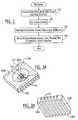
- FIGS. 3A and 3Bare top and bottom perspective views, respectively, of packages according to embodiments of the present invention, which may correspond to the cross-sectional view of FIG. 1D .
- FIGS. 3A and 3Billustrate the solid metal block 100 , the cavity 110 , the fins 190 , the first and second spaced apart conductive traces 130 a ′, 130 b ′ that wrap around the solid metal block, and the semiconductor light emitting device 150 mounted in the cavity 110 .
- the insulating coating 120may be transparent and is not shown.
- a second insulating layer and/or solder maskmay be provided on the first and/or second spaced apart conductive traces in these and/or any other embodiments.
- FIG. 4illustrates an exploded perspective view of other embodiments of the present invention, which may correspond to FIG. 1H .
- the solid metal block 100includes a cavity 110 therein, and a plurality of spaced apart electrical traces thereon.
- the first electrical trace 130 a ′is shown.
- a plurality of second electrical traces 330 a ′, 330 b ′ and 330 c ′may be provided to connect to a plurality of semiconductor light emitting devices 150 ′ that may be mounted in the cavity 110 to provide, for example, red, green and blue semiconductor light emitting devices for a white light source.
- the encapsulant 160 and lens retainer 180are shown.
- lens retainers 180can provide a ridge and/or other conventional mounting means for mounting a lens 170 on the solid metal block 100 . It also will be understood that an epoxy or other glue may be used in a lens retainer 180 . The lens retainer 180 may also provide additional top heat sinking capabilities in some embodiments of the present invention.
- FIG. 5illustrates the assembled package of FIG. 4 .
- some embodiments of the present inventionuse a solid metal block as a mounting substrate for a semiconductor light emitting device and include one or more integral cavities and a plurality of integral heat sink fins.
- Aluminum or steelhave sufficient thermal conductivity to be used as an effective heat sink when integral fins are provided. Additionally, the cost of the material and the cost of fabrication can be low. Moreover, the ability to grow high quality insulating oxides and/or provide ceramic coatings allows the desired electrical traces to be formed without a severe impact on the thermal resistance, since the thickness of the anodic oxidation or other coating can be precisely controlled.
- This insulating layeralso can be selectively patterned, which can allow the addition of another plated metal to the substrate, such as plating silver on the cavity sidewalls only, for increased optical performance.
- Embodiments of the inventionmay be particularly useful for high power semiconductor light emitting devices such as high power LEDs and/or laser diodes.
- Phosphorsmay be included in a light emitting device using many conventional techniques. In one technique, phosphor is coated inside and/or outside a plastic shell of the device. In other techniques, phosphor is coated on the semiconductor light emitting device itself, for example using electrophoretic deposition. In still other embodiments, a drop of a material such as epoxy that contains phosphor therein may be placed inside the plastic shell, on the semiconductor light emitting device and/or between the device and the shell. LEDs that employ phosphor coatings are described, for example, in U.S. Pat. Nos. 6,252,254; 6,069,440; 5,858,278; 5,813,753; 5,277,840; and 5,959,316.
- the lensincludes phosphor dispersed therein.
- FIGS. 6A-6Hare cross-sectional views of transmissive optical elements according to various embodiments of the present invention. These optical elements may be used to package semiconductor light emitting devices as will also be described below.
- transmissive optical elementsinclude a lens 170 that comprises transparent plastic.
- transparentmeans that optical radiation from the semiconductor light emitting device can pass through the material without being totally absorbed or totally reflected.
- the lens 170includes phosphor 610 dispersed therein.
- the lens 170may comprise polycarbonate material and/or other conventional plastic materials that are used to fabricate transmissive optical elements.
- the phosphor 610can comprise any conventional phosphor including cerium-doped YAG and/or other conventional phosphors.
- the phosphorcomprises Cerium doped Yttrium Aluminum Garnet (YAG:Ce). In other embodiments, nano-phosphors may be used. Phosphors are well known to those having skill in the art and need not be described further herein.
- the phosphor 610is uniformly dispersed within the lens 170 .
- the phosphor 620is nonuniformly dispersed in the lens 170 .
- Various patterns of phosphor 620may be formed, for example, to provide areas of higher intensity and/or different color and/or to provide various indicia on the lens 170 when illuminated.
- the lens 110is a dome-shaped lens.
- dome and “dome-shaped”refer to structures having a generally arcuate surface profile, including regular hemispherical structures as well as other generally arcuate structures that do not form a regular hemisphere, which are eccentric in shape and/or have other features, structures and/or surfaces.
- one or more coatings 630may be provided on the outside of the lens 170 .
- the coatingmay be a protective coating, a polarizing coating, a coating with indicia and/or any other conventional coating for an optical element that is well known to those having skill in the art.
- one or more inner coatings 640is provided on the inner surface of the lens 170 . Again, any conventional coating or combination of coatings may be used.
- embodiments of the inventionprovide both an inner and an outer coating for the lens 170 that includes uniformly distributed phosphor 610 and/or nonuniformly distributed phosphor 620 therein.
- improved index matching to the phosphormay be provided.
- three layersmay be injection molded according to some embodiments of the present invention.
- Other embodiments of the present inventioncan use an index matching media, such as a liquid and/or solid gel, within the shell, to assist in index matching.
- the use of inner and outer layerscan reduce the number of photons that can be trapped in the phosphor-containing layer due to index matching issues.
- FIG. 6Edescribes other embodiments of the present invention wherein a transparent inner core 650 is provided inside the lens 170 .
- the transparent inner core 650fills the lens 170 , to provide a hemispherical optical element.
- the transparent inner core 650may be uniformly transparent and/or may include translucent and/or opaque regions therein.
- the transparent inner core 650may comprise glass, plastic and/or other optical coupling media.
- FIG. 6Fillustrates other embodiments of the present invention wherein a phosphor-containing lens 170 is combined with a semiconductor light emitting device 150 that is configured to emit light 662 into and through the transparent inner core 650 and through the lens 170 , to emerge from the lens 170 .
- FIG. 6Gis a cross-sectional view of other embodiments of the present invention.
- a mounting substrate 100is provided, such that the light emitting device 150 is between the mounting substrate 100 and the transparent inner core 650 .
- the mounting substrate 100includes a cavity 110 therein and the light emitting device 150 is at least partially in the cavity 110 .
- Heat sink fins 190also are provided.
- FIG. 6Hillustrates yet other embodiments of the present invention.
- the cavity 110may be filled with an encapsulant 680 , such as epoxy and/or other optical coupling media (e.g., silicon).
- the encapsulant 680can enhance optical coupling from the light emitting device 150 to the transparent inner core 650 .
- Heat sink fins 190also are provided.
- FIGS. 6A-6Hhave been illustrated as separate embodiments, various elements of FIGS. 6A-6H may be used together in various combinations and subcombinations of elements.
- combinations of inner and outer coatings 640 and 630 , uniformly distributed phosphor 610 and nonuniformly distributed phosphor 620 , light emitting devices 150 , mounting substrates 100 , cavities 110 , inner cores 650 and encapsulant 680may be used together.
- embodiments of FIGS. 6A-6Hmay be combined with any other embodiments disclosed herein.
- FIG. 7is a cross-sectional view of light emitting devices according to other embodiments of the present invention.
- these embodimentsinclude a lens 170 which may be made of optically transparent material that is loaded with phosphor and/or other chemicals.
- An inner core 650may be made of optically transparent material such as plastic or glass and may be placed on an encapsulating-containing cavity 110 in a mounting substrate 100 including heat sink fins 190 .
- the lens 170 and the inner core 650form a composite lens for a light emitting diode 150 .
- FIG. 8is a schematic block diagram of an apparatus for forming transmissive optical elements according to various embodiments of the present invention.
- FIG. 8illustrates an injection molding apparatus that may be used to form transmissive optical elements according to various embodiments of the present invention.
- an injection molding apparatusincludes a hopper 810 or other storage device in which a transparent plastic and/or phosphor additive 850 are provided.
- the transparent plastic and/or phosphor additivemay be provided in pellet, powder and/or solid form.
- Other additives, such as solvents, binders, etc.may be included, as is well known to those having skill in the art.
- An injector 820may include a heater and a screw mechanism that is used to melt the transparent plastic and phosphor additive and/or maintain these materials in a melted state, to provide a molten liquid that comprises transparent plastic and the phosphor additive.
- the injector 820injects the molten liquid into a mold 840 via nozzle 830 .
- the mold 840includes an appropriate channel 860 therein, which can be used to define the shape of the optical element, such as a dome or keypad key. Injection molding of optical elements is well known to those having skill in the art and is described, for example, in U.S. Pat. Nos.
- FIG. 9is a flowchart of steps that may be used to package semiconductor light emitting devices according to various embodiments of the present invention.
- a moldsuch as mold 840 of FIG. 8
- molten liquidthat comprises a transparent plastic and a phosphor additive.
- the molten liquidis allowed to solidify to produce the optical element having phosphor dispersed therein.
- the optical elementis then removed from the mold and mounted across a cavity in a solid metal block.
- FIG. 10is a flowchart of steps that may be performed to package semiconductor light emitting devices according to embodiments of the present invention.
- a lenssuch as a dome-shaped lens 170 , that comprises a transparent plastic including a phosphor dispersed therein, is molded using injection molding, casting and/or other conventional techniques.
- a coresuch as a core 650 of FIG. 6E is formed.
- the core 650is placed or formed inside the lens 170
- Block 1020precedes Block 1010 by forming a transparent core 650 and filling a mold that includes a transparent core 650 with a molten liquid that comprises a transparent plastic and a phosphor additive, to form the lens 170 around the transparent core.
- a semiconductor light emitting devicesuch as device 150
- a mounting substratesuch as mounting substrate 100
- an encapsulantsuch as encapsulant 680 of FIG. 6H
- the lens or shellis mated to the mounting substrate using an epoxy, a snap-fit and/or other conventional mounting techniques.
- the inner core 650may fill the entire lens, so as to reduce or minimize the amount of encapsulant 680 that may be used.
- the encapsulant 680may have a different thermal expansion coefficient than the mounting substrate 100 and/or the inner core 650 .
- some embodiments of the present inventioncan form a composite optical element such as a lens using molding or casting techniques.
- injection moldingcan be used to place a phosphor layer dispersed in the molding material on the inner or outer surface and then completing the molding or casting process in the remaining volume, to form a desired optical element.
- These optical elementscan, in some embodiments, convert a blue light emitting diode behind the lens, to create the appearance of white light.
- inventions of the present inventionmay use the phosphor to evenly disperse the light and/or to disperse the light in a desired pattern.
- conventional light emitting devicesmay emit light in a “Batwing” radiation pattern, in which greater optical intensity is provided at off-axis angles, such as angles of about 40° off-axis, compared to on-axis (0°) or at the sides (for example, angles greater than about 40°).
- Other light emitting diodesmay provide a “Lambertian” radiation pattern, in which the greatest intensity is concentrated in a central area to about 40° off-axis and then rapidly drops off at larger angles.
- Still other conventional devicesmay provide a side emitting radiation pattern, wherein the greatest light intensity is provided at large angles, such as 90° from the axis, and falls rapidly at smaller angles approaching the axis.
- some embodiments of the present inventioncan reduce or eliminate angular-dependent radiation patterns of light output from a light emitting device, such as angular dependence of Color Correlated Temperature (CCT).
- CCTColor Correlated Temperature
- light intensity and the x,y chromaticity values/coordinates from all surfaces of the lenscan remain relatively constant in some embodiments. This may be advantageous when used for illumination applications, such as a room where a spotlight effect is not desirable.
- Injection molding processes as described abovecan allow formation of a single optical element with multiple features, such as lensing and white conversion. Additionally, by using a two-molding or casting technique, according to some embodiments, one can shape the phosphor layer to its desired configuration, to reduce or minimize the angular dependence of color temperature with viewing angle.
- a coating including phosphoris provided on the semiconductor light emitting device 150 itself.
- a phosphor for an LEDfor example to provide solid-state lighting.
- LEDs that are used for solid-state white lightingmay produce high radiant flux output at short wavelengths, for example in the range of about 380 nm to about 480 nm.
- One or more phosphorsmay be provided, wherein the short wavelength, high energy photon output of the LED is used to excite the phosphor, in part or entirely, to thereby down-convert in frequency some or all of the LED's output to create the appearance of white light.
- ultraviolet output from an LED at about 390 nmmay be used in conjunction with red, green and blue phosphors, to create the appearance of white light.
- blue light output at about 470 nm from an LEDmay be used to excite a yellow phosphor, to create the appearance of white light by transmitting some of the 470 nm blue output along with some secondary yellow emission occurring when part of the LEDs output is absorbed by the phosphor.
- Phosphorsmay be included in a semiconductor light emitting device using many conventional techniques.
- phosphoris coated inside and/or outside the plastic shell of an LED.
- phosphoris coated on the semiconductor light emitting device itself, for example using electrophoretic deposition.
- a drop of a material, such as epoxy that contains phosphor thereinmay be placed inside the plastic shell, on the semiconductor light emitting device and/or between the device and the shell. This technique may be referred to as a “glob top”.
- the phosphor coatingsmay also incorporate an index matching material and/or a separate index matching material may be provided.
- a light emitting diodethat includes a substrate having first and second opposing faces and a sidewall between the first and second opposing faces that extends at an oblique angle from the second face towards the first face.
- a conformal phosphor layeris provided on the oblique sidewall. The oblique sidewall can allow more uniform phosphor coatings than conventional orthogonal sidewalls.
- Semiconductor light emitting devicesare fabricated, according to other embodiments of the present invention, by placing a suspension comprising phosphor particles suspended in solvent on at least a portion of a light emitting surface of a semiconductor light emitting device, and evaporating at least some of the solvent to cause the phosphor particles to deposit on at least a portion of the light emitting surface. A coating comprising phosphor particles is thereby formed on at least a portion of the light emitting surface.
- a “suspension”means a two-phase solid-liquid system in which solid particles are mixed with, but undissolved (“suspended”), in liquid (“solvent”).
- a “solution”means a single-phase liquid system in which solid particles are dissolved in liquid (“solvent”).
- FIG. 11Ais a cross-sectional view of a semiconductor light emitting device package during an intermediate fabrication step according to various embodiments of the present invention.
- a suspension 1120 including phosphor particles 1122 suspended in solvent 1124is placed on at least a portion of a light emitting surface 150 a of a semiconductor light emitting device 150 .
- lightrefers to any radiation, visible and/or invisible (such as ultraviolet) that is emitted by a semiconductor light emitting element 150 .
- At least some of the solvent 1124is then evaporated, as shown by the arrow linking FIGS.
- the suspension 1120 including phosphor particles 1122 suspended in solvent 1124is agitated while performing the placing of FIG. 11A and/or while performing the evaporating.
- evaporatingcan be performed to cause the phosphor particles 122 to uniformly deposit on at least the portion of the light emitting surface 150 a , to thereby form a uniform coating 1130 of the phosphor particles 1122 .
- the phosphor particles 1122uniformly deposit on all the light emitting surface 150 a .
- substantially all of the solvent 1124can be evaporated. For example, in some embodiments, at least about 80% of the solvent can be evaporated. In some embodiments, substantially all the solvent 1124 is evaporated to cause the phosphor particles 1122 to uniformly deposit on all the light emitting surface 150 a.
- the solvent 1124comprises Methyl Ethyl Ketone (MEK), alcohol, toluene, Amyl Acetate and/or other conventional solvents.
- the phosphor particles 1122may be about 3-4 ⁇ m in size, and about 0.2 gm of these phosphor particles 1122 may be mixed into about Sec of MEK solvent 1124 , to provide the suspension 1120 .
- the suspension 1120may be dispensed via an eyedropper pipette, and evaporation may take place at room temperature or at temperatures above or below room temperature, such as at about 60° C. and/or at about 100° C.
- the phosphor particles 1122may be Cerium-doped Yttrium Aluminum Garnet (YAG:Ce) and/or other conventional phosphors and may be mixed into the solvent 1124 using conventional mixing techniques, to thereby provide the suspension 1120 comprising phosphor particles 1122 .
- the phosphoris configured to convert at least some light that is emitted from the light emitting surface 150 a such that light that emerges from the semiconductor light emitting device appears as white light.
- FIG. 12Ais a cross-sectional view of other embodiments of the present invention.
- a mounting substrate 100is provided, and the semiconductor light emitting element 150 is mounted in a cavity 110 therein.
- Heat sink fins 190also are provided.
- the suspension 1120 including phosphor particles 1122 suspended in solvent 1124is placed in the cavity 110 .
- the cavity 110can be used to confine the suspension 1120 and thereby provide a controlled amount and geometry for the suspension 1120 .
- evaporationis performed, to thereby evaporate at least some of the solvent 1124 to cause the phosphor particles 1122 to deposit on at least a portion of the light emitting surface 150 a , and form a coating 1130 including the phosphor particles 1122 .
- FIGS. 13A and 13Billustrate other embodiments of the present invention.
- the cavity 110includes a cavity floor 110 b
- the semiconductor light emitting device 150is mounted on the cavity floor 110 b .
- the semiconductor light emitting device 150protrudes away from the cavity floor 110 b .
- the light emitting surface 150 a of the semiconductor light emitting device 150includes a face 150 b that is remote from the cavity floor 110 b , and a sidewall 150 c that extends between the face 150 b and the cavity floor 110 b . As shown in FIG.
- evaporatingis performed to evaporate at least some of the solvent 1124 , to cause the phosphor particles 1122 to uniformly deposit on at least a portion of the light emitting surface 150 a and thereby form a coating 1130 of uniform thickness comprising the phosphor particles 1122 .
- the coatingmay be of uniform thickness on the face 150 b and on the sidewall 150 c .
- the coating 1130may extend uniformly on the floor 110 b outside the light emitting element 150 . In other embodiments, the coating 1130 also may extend at least partially onto sidewalls 110 a of the cavity 110 .
- a bindermay be added to the suspension 1120 so that, upon evaporation, the phosphor particles 1122 and the binder deposit on at least the portion of the light emitting surface 150 a , and form a coating thereon comprising the phosphor particles 1122 and the binder.
- a cellulose materialsuch as ethyl cellulose and/or nitro cellulose, may be used as a binder.
- at least some of the bindermay evaporate along with the solvent.
- the suspension 1120includes the phosphor particles 1122 and light scattering particles suspended in solvent 1124 , and wherein at least some of the solvent 1124 is evaporated to cause the phosphor particles 1122 and the light scattering particles to deposit on at least a portion of the light emitting device 150 , and form a coating 1130 including the phosphor particles 1122 and the light scattering particles.
- the light scattering particlesmay include SiO 2 (glass) particles. By selecting the size of the scattering particles, blue light may be effectively scattered to make the emission source (for white applications) more uniform (more specifically, random), in some embodiments.
- FIGS. 11A-13Balso may be provided, according to various embodiments of the invention.
- combinations and subcombinations of embodiments of FIGS. 11A-13B with any or all of the other figuresalso may be provided according to various embodiments of the invention.
- Other embodiments of coating a semiconductor light emitting device by evaporating solvents from a suspensionare described in application Ser. No. 10/946,587, filed Sep. 21, 2004, entitled Methods of Coating Semiconductor Light Emitting Elements by Evaporating Solvent From a Suspension, assigned to the assignee of the present invention, the disclosure of which is hereby incorporated herein by reference in its entirety as if set forth fully herein.
- a flexible filmthat includes an optical element therein on the first metal face, wherein the optical element extends across the cavity.
- the optical elementis a lens.
- the optical elementmay include a phosphor coating and/or may include phosphor dispersed therein.
- FIG. 14is an exploded cross-sectional view of semiconductor light emitting device packages and assembling methods therefor, according to various embodiments of the present invention.
- these semiconductor light emitting device packagesinclude a solid metal block 100 having a first face 100 a including a cavity 110 therein, and a second face 100 b , including a plurality of heat sink fins 190 therein.
- a flexible film 1420including therein an optical element 1430 , is provided on the first face 100 a
- a semiconductor light emitting device 150is provided between the metal block 100 and the flexible film 1120 , and configured to emit light 662 through the optical element.
- An attachment element 1450may be used to attach the flexible film 1420 and the solid metal block 100 to one another.
- the flexible film 1420can provide a cover slip that can be made of a flexible material such as a conventional Room Temperature Vulcanizing (RTV) silicone rubber. Other silicone-based and/or flexible materials may be used. By being made of a flexible material, the flexible film 1420 can conform to the solid metal block 100 as it expands and contracts during operations. Moreover, the flexible film 1420 can be made by simple low-cost techniques such as transfer molding, injection molding and/or other conventional techniques that are well known to those having skill in the art.
- RTVRoom Temperature Vulcanizing
- the flexible film 1420includes therein an optical element 1430 .
- the optical elementcan include a lens, a prism, an optical emission enhancing and/or converting element, such as a phosphor, an optical scattering element and/or other optical element.
- One or more optical elements 1430also may be provided, as will be described in detail below.
- an optical coupling media 1470such as an optical coupling gel and/or other index matching material, may be provided between the optical element 1430 and the semiconductor light emitting device 150 , in some embodiments.
- the attachment element 1450can be embodied as an adhesive that may be placed around the periphery of the solid metal block 100 , around the periphery of the flexible film 1420 and/or at selected portions thereof, such as at the corners thereof.
- the solid metal block 100may be coined around the flexible film 1420 , to provide an attachment element 1450 .
- Other conventional attaching techniquesmay be used.
- FIG. 14also illustrates methods of assembling or packaging semiconductor light emitting devices according to various embodiments of the present invention.
- a semiconductor light emitting element 150is mounted in a cavity 110 in a first face 100 a of a solid metal block 100 that includes fins 190 on a second face 100 b thereof.
- a flexible film 1420 that includes therein an optical element 1430is attached to the first face 100 a , for example using an attachment element 1450 , such that, in operation, the semiconductor light emitting device 150 emits light 662 through the optical element 1430 .
- an optical coupling media 1470is placed between the semiconductor light emitting device 150 and the optical element 1430 .
- FIG. 15is a cross-sectional view of packaged semiconductor light emitting devices of FIG. 14 , according to other embodiments of the present invention.
- the flexible film 1420extends onto the face 100 a beyond the cavity 110 .
- the optical element 1430overlies the cavity 110 , and the semiconductor light emitting device 150 is in the cavity 110 , and is configured to emit light 662 through the optical element 1430 .
- the optical element 1430includes a concave lens.
- an optical coupling media 1470is provided in the cavity 110 between the optical element 1430 and the semiconductor light emitting device 150 .
- the optical coupling media 1470fills the cavity 110 .
- FIG. 16is a cross-sectional view of other embodiments of the present invention.
- two optical elements 1430 and 1630are included in the flexible film 1420 .
- a first optical element 1430includes a lens and a second optical element 1630 includes a prism.
- Light from the semiconductor light emitting device 150passes through the prism 1630 and through the lens 1430 .
- An optical coupling media 1470also may be provided. In some embodiments, the optical coupling media 1470 fills the cavity 110 .
- the optical coupling media 1470may have a sufficient difference in index of refraction from the prism 1630 such that the prism 1630 can reduce shadowing. As shown in FIG.
- the semiconductor light emitting device 150includes a wire 1650 that extends towards the flexible film 1420 , and the prism 1630 is configured to reduce shadowing by the wire 1650 of the light that is emitted from the semiconductor light emitting device 150 . More uniform light emissions thereby may be provided, with reduced shadowing of the wire 1650 .
- wireis used herein in a generic sense to encompass any electrical connection for the semiconductor light emitting device 150 .
- FIG. 17is a cross-sectional view of other embodiments of the present invention.
- phosphor 1710is provided on the flexible film 1320 between the lens 1430 and the semiconductor light emitting device 150 .
- the phosphor 410can include cerium-doped Yttrium Aluminum Garnet (YAG) and/or other conventional phosphors.
- the phosphorcomprises Cerium doped Yttrium Aluminum Garnet (YAG:Ce).
- nano-phosphorsmay be used. Phosphors are well known to those having skill in the art and need not be described further herein.
- An optical coupling media 1470also may be provided that may fill the cavity 110 .
- FIG. 18illustrates yet other embodiments of the present invention.
- the lens 1430includes a concave inner surface 1430 a adjacent the semiconductor light emitting device 150
- the phosphor 1710includes a conformal phosphor layer on the concave inner surface 1430 a .
- An optical coupling media 1470also may be provided that may fill the cavity 110 .
- FIG. 19is a cross-sectional view of other embodiments. As shown in FIG. 19 , at least a portion 1420 d of the flexible film 1420 that overlies the cavity 110 is transparent to the light. Moreover, at least a portion 1420 c of the flexible film 1420 that extends onto the face 100 a beyond the cavity 110 is opaque to the light, as shown by the dotted portions 1420 c of the flexible film 1420 . The opaque regions 1420 c can reduce or prevent bouncing of light rays, and thereby potentially produce a more desirable light pattern. An optical coupling media 1470 also may be provided that may fill the cavity 110 .
- FIG. 20is a cross-sectional view of other embodiments of the present invention wherein the flexible film 1420 may be fabricated of multiple materials. As shown in FIG. 20 , at least a portion 1420 d of the flexible film 1420 that overlies the cavity 110 includes a first material, and at least a portion 1420 c of the flexible film 1420 that extends onto the face 100 a beyond the cavity 110 includes a second material. Two or more materials may be used in the flexible film 1420 in some embodiments, to provide different characteristics for the portion of the flexible film 1420 through which light is emitted and through which light is not emitted. Multiple materials may be used for other purposes in other embodiments. For example, an inflexible and/or flexible plastic lens may be attached to a flexible film.
- Such a flexible film 1420 with multiple materialsmay be fabricated using conventional multiple molding techniques, for example.
- the first material that is moldedmay not be fully cured, so as to provide a satisfactory bond that attaches to the second material that is subsequently molded.
- the same materialmay be used for the optical element and the flexible film, wherein the optical element is formed and then the flexible film is formed surrounding the optical element.
- An optical coupling media 1470also may be provided that may fill the cavity 110 .
- FIG. 21is a cross-sectional view of other embodiments of the present invention.
- the semiconductor light emitting element 150includes a wire 1650 , that extends towards and contacts the flexible film 1420 in the cavity 110 .
- the flexible film 1420includes a transparent conductor 2110 which can include Indium Tin Oxide (ITO) and/or other conventional transparent conductors.
- ITOIndium Tin Oxide
- the transparent conductor 2110extends in the cavity 110 and electrically connects to the wire. Reduced shadowing by the wire 1650 thereby may be provided. Moreover, a wire bond to the metal block 100 , and the potential consequent light distortion, may be reduced or eliminated.
- An optical coupling media 1470also may be provided that may fill the cavity 110 .
- FIG. 22is a cross-sectional view of other embodiments of the present invention.
- the optical element 1430includes a lens that overlies the cavity 110 and protrudes away from the cavity 110 .
- the flexible film 1420further includes a protruding element 2230 between the lens 1430 and the light emitting element 150 that protrudes towards the cavity 110 .
- a conformal phosphor layer 1710is provided on the protruding element 2230 .
- optical coupling media 1470 in the devicemay be displaced. Arrangements of FIG. 22 may thus provide more uniform phosphor coating at desired distances from the light emitting element 150 , so as to provide more uniform illumination.
- the optical coupling media 1470may fill the cavity 110 .
- FIGS. 23 and 24illustrate packages including multiple semiconductor light emitting devices and/or multiple optical elements according to various embodiments of the present invention.
- the optical element 1430is a first optical element
- the semiconductor light emitting device 150is a first semiconductor light emitting device.
- the flexible film 1420also includes therein a second optical element 1430 ′ that is spaced apart from the first optical element 1430 , and the device further includes a second semiconductor light emitting device 150 ′ between the substrate 100 and the flexible film 1420 , and configured to emit light through the second optical element 1430 ′.
- a third optical element 1430 ′′ and a third semiconductor light emitting device 150 ′′also may be provided.
- the optical elements 1430 , 1430 ′ and 1430 ′′may be the same and/or different from one another, and the semiconductor light emitting devices 150 , 150 ′ and 150 ′′ may be the same and/or different from one another.
- the cavity 110is a first cavity, and second and third cavities 110 ′, 110 ′′, respectively, are provided for the second and third semiconductor light emitting devices 150 ′, 150 ′′, respectively.
- the cavities 110 , 110 ′ and 110 ′′may be the same and/or may have different configurations from one another.
- An optical coupling media 1470also may be provided that may fill the cavity or cavities. It will be understood that larger or smaller numbers of semiconductor light emitting devices and/or cavities may be provided in other embodiments.
- the phosphor 1710may be a first phosphor layer, and second and/or third phosphor layers 1710 ′ and 1710 ′′, respectively, may be provided on the flexible film 1420 between the second optical element 1430 ′ and the second semiconductor light emitting device 150 ′, and between the third optical element 1430 ′′ and the third semiconductor light emitting device 150 ′′, respectively.
- the phosphor layers 1710 , 1710 ′, 1710 ′′may be the same, may be different and/or may be eliminated.
- the first phosphor layer 1710 and the first semiconductor light emitting device 150are configured to generate red light
- the second phosphor layer 1710 ′ and the second semiconductor light emitting device 150 ′are configured to generate blue light
- the third phosphor layer 1710 ′′ and the third semiconductor light emitting device 150 ′′are configured to generate green light.
- a Red, Green, Blue (RGB) light emitting element that can emit white lightthereby may be provided in some embodiments.
- FIG. 24is a cross-sectional view of other embodiments of the present invention.
- a single cavity 2400is provided for the first, second and third semiconductor light emitting devices 150 , 150 ′ and 150 ′′, respectively.
- An optical coupling media 1470also may be provided that may fill the cavity 2400 . It will be understood that larger or smaller numbers of semiconductor light emitting devices and/or cavities may be provided in other embodiments.
- FIG. 25is a cross-sectional view of yet other embodiments of the present invention.
- the optical element 2530comprises a lens having phosphor dispersed therein. Many embodiments of lenses including phosphor dispersed therein were described above and need not be repeated.
- an optical scattering elementmay be embedded in the lens as shown in FIG. 25 , and/or provided as a separating layer as shown, for example, in FIG. 22 , in addition or instead of phosphor.
- FIG. 26is a perspective view of a semiconductor light emitting device package according to other embodiments of the present invention.
- FIGS. 14-26It will be understood by those having skill in the art that various embodiments of the invention have been described individually in connection with FIGS. 14-26 . However, combinations and subcombinations of the embodiments of FIGS. 14-26 may be provided according to various embodiments of the present invention, and also may be combined with embodiments according to any of the other figures described herein.
- FIG. 27is a cross-sectional view of a semiconductor light emitting device package according to various embodiments of the present invention.
- a solid metal block 100includes a plurality of cavities 110 in a first metal face 100 a thereof, and a plurality of heat sink fins 190 in a second metal face 100 b thereof.
- An insulating layer 120is provided on the first metal face 100 a .
- a conductive layer 130is provided on the insulating layer, and is patterned to provide a reflective coating 2730 a in the cavity 110 , and first 2730 b and second 2730 c conductive traces in the cavity 110 that are configured to connect to at least one semiconductor light emitting device 150 that is mounted in the cavity.
- FIG. 1is a cross-sectional view of a semiconductor light emitting device package according to various embodiments of the present invention.
- a solid metal block 100includes a plurality of cavities 110 in a first metal face 100 a thereof, and a plurality of heat sink fins 190 in a second metal
- the tracescan provide series connection between the semiconductor light emitting devices.
- parallel and/or series/parallel or anti-parallel connectionsalso may be provided. It will be understood that larger or smaller numbers of semiconductor light emitting devices and/or cavities may be provided in other embodiments.
- Various embodiments of flexible films 1420 and optical elements 1430may be provided as was described extensively above.
- phosphormay be integrated as was described extensively above.
- discrete lenses 170also may be provided, instead of the flexible film 1420 containing optical elements 1430 .
- the conductor 130is connected to an integrated circuit 2710 , such as the light emitting device driver integrated circuit, on the solid metal block 110 .
- a semiconductor light emitting package of FIG. 27can be configured to provide a plug-in substitute for a conventional light bulb.
- FIG. 28is a perspective view of embodiments according to FIG. 27 .
- an array of cavities 110 that are connected by a conductive layer 130may be provided on the first face 100 a of a solid metal block 100 .
- a uniformly spaced 10% 10 array of cavities and a corresponding 10% 10 array of optical elements 1430 on a flexible film 1420is shown.
- larger or smaller arraysmay be provided and the arrays may be circular, randomly spaced and/or of other configuration.
- nonuniform spacingmay be provided in some or all portions of the array of cavities 110 and optical elements 1430 . More specifically, uniform spacing may promote uniform light output, whereas nonuniform spacing may be provided to compensate for variations in heat dissipation abilities of the heat sink fins 190 across various portions of the solid metal block 100 .
- FIGS. 27 and 28may be combined in various combinations and subcombinations with any of the other embodiments described herein.
- FIG. 29is a side cross-sectional view of other embodiments of the present invention.
- the first metal face 100 afurther includes a plurality of pedestals 2900 therein, and a respective one of the plurality of cavities 110 is in a respective one of the plurality of pedestals 2900 .
- the insulating layer 120 and conductive layer 130are not illustrated in FIG. 29 for the sake of clarity. Multiple cavities 110 also may be provided in a given pedestal 2900 in other embodiments.
- the flexible film 1420 ′includes a plurality of optical elements 1430 ′, such as lenses, a respective one of which extends across a respective pedestal 2900 and across a respective cavity 110 . It will be understood that larger or smaller numbers of semiconductor light emitting devices and/or cavities may be provided in other embodiments.
- the light emitting devices 150may be placed closer to the radial center of the optical elements 1430 ′, to thereby allow the uniformity of emissions to be enhanced.
- embodiments of FIG. 29may be provided with discrete optical elements, such as lenses, a respective one of which spans across a respective pedestal 2900 and cavity 110 , and that embodiments of FIG. 29 may be combined with any combination or subcombination of the other embodiments that were described above.
- FIG. 30is a flowchart of steps that may be performed to package semiconductor light emitting devices according to various embodiments of the present invention. Methods of FIG. 30 may be used to package one or more semiconductor light emitting devices, to provide structures that were described in any of the preceding figures.
- a solid metal block including cavities and heat sink finsis fabricated, as was described extensively above.
- An insulating layeris formed on at least a portion of the solid metal block, for example on the first metal face thereof, at Block 3020 , as was described extensively above.
- a conductive layeris formed on the insulating layer. The conductive layer may be patterned to provide a reflective coating in the cavities, and first and second conductive traces on the first face that extend into the cavities, as was described extensively above.
- at least one semiconductor light emitting deviceis mounted in a respective cavity, and electrically connected to the first and second conductive traces in the respective cavity, as was described extensively above.
- an optical coupling mediummay be added, as was described above.
- a lens, optical element and/or flexible filmis placed on the first face, as was described extensively above.
- through holes, reflector layers and/or other structures that were described extensively above,also may be provided.
- Embodiments of the present inventioncan provide a three-dimensional topside and backside topology on solid metal blocks, to thereby provide integral reflector cavities and integral heat sinks all in one piece.
- the integrated optical cavitiesmay facilitate alignment and ease of manufacturing.
- the integral heat sinkmay enhance thermal efficiency.
- a three-dimensional topside topologyto form reflectors for the LEDs, the need to individually package the LEDs, mount the package to a heat sink and add the desired drive electronics may be eliminated, according to some embodiments of the present invention.
- a “chip on integral reflector heat sink”may be provided as a single component. High optical efficiency and high thermal efficiency thereby may be provided.
- Adding the drive circuitrycan provide a complete solution for a functional luminary that may only need a source voltage and a final luminary housing.
- Any shape or density devicemay be provided.
- a high density embodimentmay have four high power LEDs such as are marketed under the designation XB900 by Cree, Inc., the assignee of the present invention, to provide a 2% 2 array, while a distributed thermal approach may have 100 lower power LEDs, such as are marketed under the designation XB290 by Cree, Inc., the assignee of the present invention, to provide a 10% 10 array, to achieve the same lumen output.
- the XB900 and XB290 devicesare described in a product brochure entitled Cree Optoelectronics LED Product Line, Publication CPR3AX, Rev. D, 2001-2002.
- Other devices that are described in this product brochure, such as XT290, XT230 and/or other devices from other manufacturersalso may be used.
- the optical cavitiesmay be either recessed or may be provided as optical cavities in pedestals.
- the conductive layercan provide die-attach pads and wire bond pads. Separate traces may be provided for red, green or blue LEDs, or all the LEDs may be connected in series or in parallel.
- Embodiments of the present inventioncan provide a configuration that may be able to replace a standard MR16 or other light fixture.
- 6.4 watts inputmay provide about 2.4 watts of optical power and 4 watts of heat dissipation.
Landscapes
- Engineering & Computer Science (AREA)
- General Engineering & Computer Science (AREA)
- Led Device Packages (AREA)
- Semiconductor Lasers (AREA)
Abstract
Description
Claims (28)
Priority Applications (3)
| Application Number | Priority Date | Filing Date | Title |
|---|---|---|---|
| US12/363,000US8598606B2 (en) | 2004-10-25 | 2009-01-30 | Solid metal block semiconductor light emitting device mounting substrates and packages |
| US12/484,713US7906793B2 (en) | 2004-10-25 | 2009-06-15 | Solid metal block semiconductor light emitting device mounting substrates |
| US13/074,942US20110210360A1 (en) | 2004-10-25 | 2011-03-29 | Transmissive optical elements including phosphor patterns therein |
Applications Claiming Priority (2)
| Application Number | Priority Date | Filing Date | Title |
|---|---|---|---|
| US10/972,910US20060097385A1 (en) | 2004-10-25 | 2004-10-25 | Solid metal block semiconductor light emitting device mounting substrates and packages including cavities and heat sinks, and methods of packaging same |
| US12/363,000US8598606B2 (en) | 2004-10-25 | 2009-01-30 | Solid metal block semiconductor light emitting device mounting substrates and packages |
Related Parent Applications (1)
| Application Number | Title | Priority Date | Filing Date |
|---|---|---|---|
| US10/972,910ContinuationUS20060097385A1 (en) | 2004-10-25 | 2004-10-25 | Solid metal block semiconductor light emitting device mounting substrates and packages including cavities and heat sinks, and methods of packaging same |
Related Child Applications (2)
| Application Number | Title | Priority Date | Filing Date |
|---|---|---|---|
| US12/484,713ContinuationUS7906793B2 (en) | 2004-10-25 | 2009-06-15 | Solid metal block semiconductor light emitting device mounting substrates |
| US13/074,942ContinuationUS20110210360A1 (en) | 2004-10-25 | 2011-03-29 | Transmissive optical elements including phosphor patterns therein |
Publications (2)
| Publication Number | Publication Date |
|---|---|
| US20090134421A1 US20090134421A1 (en) | 2009-05-28 |
| US8598606B2true US8598606B2 (en) | 2013-12-03 |
Family
ID=36097284
Family Applications (4)
| Application Number | Title | Priority Date | Filing Date |
|---|---|---|---|
| US10/972,910AbandonedUS20060097385A1 (en) | 2004-10-25 | 2004-10-25 | Solid metal block semiconductor light emitting device mounting substrates and packages including cavities and heat sinks, and methods of packaging same |
| US12/363,000Active2026-10-29US8598606B2 (en) | 2004-10-25 | 2009-01-30 | Solid metal block semiconductor light emitting device mounting substrates and packages |
| US12/484,713Expired - LifetimeUS7906793B2 (en) | 2004-10-25 | 2009-06-15 | Solid metal block semiconductor light emitting device mounting substrates |
| US13/074,942AbandonedUS20110210360A1 (en) | 2004-10-25 | 2011-03-29 | Transmissive optical elements including phosphor patterns therein |
Family Applications Before (1)
| Application Number | Title | Priority Date | Filing Date |
|---|---|---|---|
| US10/972,910AbandonedUS20060097385A1 (en) | 2004-10-25 | 2004-10-25 | Solid metal block semiconductor light emitting device mounting substrates and packages including cavities and heat sinks, and methods of packaging same |
Family Applications After (2)
| Application Number | Title | Priority Date | Filing Date |
|---|---|---|---|
| US12/484,713Expired - LifetimeUS7906793B2 (en) | 2004-10-25 | 2009-06-15 | Solid metal block semiconductor light emitting device mounting substrates |
| US13/074,942AbandonedUS20110210360A1 (en) | 2004-10-25 | 2011-03-29 | Transmissive optical elements including phosphor patterns therein |
Country Status (8)
| Country | Link |
|---|---|
| US (4) | US20060097385A1 (en) |
| EP (2) | EP1805807A2 (en) |
| JP (2) | JP2008518461A (en) |
| KR (1) | KR101203818B1 (en) |
| CN (1) | CN101048880A (en) |
| AU (1) | AU2005300077A1 (en) |
| TW (2) | TWI460877B (en) |
| WO (1) | WO2006046981A2 (en) |
Cited By (3)
| Publication number | Priority date | Publication date | Assignee | Title |
|---|---|---|---|---|
| US20130229800A1 (en)* | 2004-12-17 | 2013-09-05 | Lg Innotek Co., Ltd. | Package for light emitting device and method for packaging the same |
| US20130298396A1 (en)* | 2011-11-09 | 2013-11-14 | Xiaofeng Bi | Method of making a heat radiating structure for high-power led |
| US20180132353A1 (en)* | 2015-05-29 | 2018-05-10 | Thales | Electronic board and associated manufacturing method |
Families Citing this family (300)
| Publication number | Priority date | Publication date | Assignee | Title |
|---|---|---|---|---|
| US7775685B2 (en) | 2003-05-27 | 2010-08-17 | Cree, Inc. | Power surface mount light emitting die package |
| US7244965B2 (en)* | 2002-09-04 | 2007-07-17 | Cree Inc, | Power surface mount light emitting die package |
| US7837348B2 (en) | 2004-05-05 | 2010-11-23 | Rensselaer Polytechnic Institute | Lighting system using multiple colored light emitting sources and diffuser element |
| AU2005240186B2 (en)* | 2004-05-05 | 2011-02-03 | Rensselaer Polytechnic Institute | High efficiency light source using solid-state emitter and down-conversion material |
| US20060097385A1 (en)* | 2004-10-25 | 2006-05-11 | Negley Gerald H | Solid metal block semiconductor light emitting device mounting substrates and packages including cavities and heat sinks, and methods of packaging same |
| US7772609B2 (en)* | 2004-10-29 | 2010-08-10 | Ledengin, Inc. (Cayman) | LED package with structure and materials for high heat dissipation |
| US9929326B2 (en) | 2004-10-29 | 2018-03-27 | Ledengin, Inc. | LED package having mushroom-shaped lens with volume diffuser |
| US7670872B2 (en)* | 2004-10-29 | 2010-03-02 | LED Engin, Inc. (Cayman) | Method of manufacturing ceramic LED packages |
| US8134292B2 (en)* | 2004-10-29 | 2012-03-13 | Ledengin, Inc. | Light emitting device with a thermal insulating and refractive index matching material |
| US8816369B2 (en) | 2004-10-29 | 2014-08-26 | Led Engin, Inc. | LED packages with mushroom shaped lenses and methods of manufacturing LED light-emitting devices |
| US7473933B2 (en)* | 2004-10-29 | 2009-01-06 | Ledengin, Inc. (Cayman) | High power LED package with universal bonding pads and interconnect arrangement |
| US8324641B2 (en) | 2007-06-29 | 2012-12-04 | Ledengin, Inc. | Matrix material including an embedded dispersion of beads for a light-emitting device |
| US8541797B2 (en)* | 2004-11-18 | 2013-09-24 | Koninklijke Philips N.V. | Illuminator and method for producing such illuminator |
| US7322732B2 (en) | 2004-12-23 | 2008-01-29 | Cree, Inc. | Light emitting diode arrays for direct backlighting of liquid crystal displays |
| US9070850B2 (en) | 2007-10-31 | 2015-06-30 | Cree, Inc. | Light emitting diode package and method for fabricating same |
| US9412926B2 (en)* | 2005-06-10 | 2016-08-09 | Cree, Inc. | High power solid-state lamp |
| US7980743B2 (en)* | 2005-06-14 | 2011-07-19 | Cree, Inc. | LED backlighting for displays |
| CA2597697C (en)* | 2005-06-23 | 2014-12-02 | Rensselaer Polytechnic Institute | Package design for producing white light with short-wavelength leds and down-conversion materials |
| US20060292747A1 (en)* | 2005-06-27 | 2006-12-28 | Loh Ban P | Top-surface-mount power light emitter with integral heat sink |
| KR100653605B1 (en)* | 2005-11-15 | 2006-12-06 | 삼성전자주식회사 | Semiconductor chip package having a metal core heat sink and a semiconductor module comprising the same |
| KR101358699B1 (en)* | 2006-01-24 | 2014-02-07 | 코닌클리케 필립스 엔.브이. | Light-emitting device |
| KR101210090B1 (en)* | 2006-03-03 | 2012-12-07 | 엘지이노텍 주식회사 | Metal core printed circuit board and light-emitting diode packaging method thereof |
| US7675145B2 (en) | 2006-03-28 | 2010-03-09 | Cree Hong Kong Limited | Apparatus, system and method for use in mounting electronic elements |
| WO2007139781A2 (en) | 2006-05-23 | 2007-12-06 | Cree Led Lighting Solutions, Inc. | Lighting device |
| CN101449391B (en) | 2006-05-30 | 2011-02-23 | 株式会社藤仓 | A base plate for mounting a luminous element, a light source, a lighting device, a display device, a piece of traffic signalling equipment and a manufacturing method of the base plate for mounting the |
| US20080035942A1 (en)* | 2006-08-08 | 2008-02-14 | Lg Electronics Inc. | Light emitting device package and method for manufacturing the same |
| EP2056364A4 (en)* | 2006-08-11 | 2013-07-24 | Mitsubishi Chem Corp | LIGHTING APPARATUS |
| US7703942B2 (en)* | 2006-08-31 | 2010-04-27 | Rensselaer Polytechnic Institute | High-efficient light engines using light emitting diodes |
| US7952262B2 (en)* | 2006-09-30 | 2011-05-31 | Ruud Lighting, Inc. | Modular LED unit incorporating interconnected heat sinks configured to mount and hold adjacent LED modules |
| US9243794B2 (en) | 2006-09-30 | 2016-01-26 | Cree, Inc. | LED light fixture with fluid flow to and from the heat sink |
| US7686469B2 (en) | 2006-09-30 | 2010-03-30 | Ruud Lighting, Inc. | LED lighting fixture |
| US20090086491A1 (en) | 2007-09-28 | 2009-04-02 | Ruud Lighting, Inc. | Aerodynamic LED Floodlight Fixture |
| US9028087B2 (en) | 2006-09-30 | 2015-05-12 | Cree, Inc. | LED light fixture |
| US8497560B2 (en)* | 2006-10-06 | 2013-07-30 | Industrial Technology Research Institute | LED package and method of assembling the same |
| US7889421B2 (en) | 2006-11-17 | 2011-02-15 | Rensselaer Polytechnic Institute | High-power white LEDs and manufacturing method thereof |
| US20080121911A1 (en)* | 2006-11-28 | 2008-05-29 | Cree, Inc. | Optical preforms for solid state light emitting dice, and methods and systems for fabricating and assembling same |
| CN100433391C (en)* | 2006-11-30 | 2008-11-12 | 何永祥 | A large power LED using porous metal material as heat emission device |
| DE102006062066A1 (en)* | 2006-12-29 | 2008-07-03 | Osram Opto Semiconductors Gmbh | Lens arrangement for light emitting diode display device, has lens with lens surface and optical axis, which penetrates lens surface of lens |
| US9711703B2 (en) | 2007-02-12 | 2017-07-18 | Cree Huizhou Opto Limited | Apparatus, system and method for use in mounting electronic elements |
| US20080283864A1 (en)* | 2007-05-16 | 2008-11-20 | Letoquin Ronan P | Single Crystal Phosphor Light Conversion Structures for Light Emitting Devices |
| TW200847469A (en)* | 2007-05-23 | 2008-12-01 | Tysun Inc | Substrates of curved surface for light emitting diodes |
| KR100888228B1 (en)* | 2007-06-22 | 2009-03-12 | (주)웨이브닉스이에스피 | Metal-Based Photonic Device Package Module and Process of The Same |
| US20090039382A1 (en)* | 2007-08-10 | 2009-02-12 | Iintematix Technology Center Corp. | Light emitting diode package structure |
| US7810956B2 (en)* | 2007-08-23 | 2010-10-12 | Koninklijke Philips Electronics N.V. | Light source including reflective wavelength-converting layer |
| US20090059594A1 (en)* | 2007-08-31 | 2009-03-05 | Ming-Feng Lin | Heat dissipating apparatus for automotive LED lamp |
| US10256385B2 (en) | 2007-10-31 | 2019-04-09 | Cree, Inc. | Light emitting die (LED) packages and related methods |
| US8866169B2 (en) | 2007-10-31 | 2014-10-21 | Cree, Inc. | LED package with increased feature sizes |
| US20090121244A1 (en)* | 2007-11-08 | 2009-05-14 | Steven Lo | LED packaging structure and production method thereof |
| US9754926B2 (en) | 2011-01-31 | 2017-09-05 | Cree, Inc. | Light emitting diode (LED) arrays including direct die attach and related assemblies |
| US9640737B2 (en) | 2011-01-31 | 2017-05-02 | Cree, Inc. | Horizontal light emitting diodes including phosphor particles |
| US9660153B2 (en) | 2007-11-14 | 2017-05-23 | Cree, Inc. | Gap engineering for flip-chip mounted horizontal LEDs |
| TWI389294B (en)* | 2008-03-07 | 2013-03-11 | Harvatek Corp | A package structure for manufacturing a light emitting diode chip which reduces the luminous efficiency of a phosphor due to high temperature and a method of manufacturing the same |
| TW200941761A (en)* | 2008-03-27 | 2009-10-01 | Liung Feng Ind Co Ltd | Packaging process of a light emitting component |
| CN101552311B (en)* | 2008-04-03 | 2011-11-30 | 良峰塑胶机械股份有限公司 | Packaging process of light-emitting elements |
| US8008682B2 (en)* | 2008-04-04 | 2011-08-30 | Hong Kong Applied Science And Technology Research Institute Co. Ltd. | Alumina substrate and method of making an alumina substrate |
| KR100992778B1 (en)* | 2008-05-23 | 2010-11-05 | 엘지이노텍 주식회사 | Light emitting device package and method for manufacturing the same |
| US7868340B2 (en)* | 2008-05-30 | 2011-01-11 | Bridgelux, Inc. | Method and apparatus for generating white light from solid state light emitting devices |
| CN101598312A (en)* | 2008-06-06 | 2009-12-09 | 富准精密工业(深圳)有限公司 | LED structure |
| US20100006873A1 (en)* | 2008-06-25 | 2010-01-14 | Soraa, Inc. | HIGHLY POLARIZED WHITE LIGHT SOURCE BY COMBINING BLUE LED ON SEMIPOLAR OR NONPOLAR GaN WITH YELLOW LED ON SEMIPOLAR OR NONPOLAR GaN |
| TW201000819A (en)* | 2008-06-30 | 2010-01-01 | Create Electronic Optical Co Ltd | LED illumination device |
| US7728399B2 (en)* | 2008-07-22 | 2010-06-01 | National Semiconductor Corporation | Molded optical package with fiber coupling feature |
| US9076951B2 (en) | 2008-08-26 | 2015-07-07 | Albeo Technologies, Inc. | Methods of integrating LED chips with heat sinks, and LED-based lighting assemblies made thereby |
| US8981629B2 (en)* | 2008-08-26 | 2015-03-17 | Albeo Technologies, Inc. | Methods of integrating LED chips with heat sinks, and LED-based lighting assemblies made thereby |
| JP4881358B2 (en) | 2008-08-28 | 2012-02-22 | 株式会社東芝 | Light emitting device |
| TW201011936A (en)* | 2008-09-05 | 2010-03-16 | Advanced Optoelectronic Tech | Light emitting device and fabrication thereof |
| US8188486B2 (en)* | 2008-09-16 | 2012-05-29 | Osram Sylvania Inc. | Optical disk for lighting module |
| US9252336B2 (en)* | 2008-09-26 | 2016-02-02 | Bridgelux, Inc. | Multi-cup LED assembly |
| US8075165B2 (en)* | 2008-10-14 | 2011-12-13 | Ledengin, Inc. | Total internal reflection lens and mechanical retention and locating device |
| US20100117106A1 (en)* | 2008-11-07 | 2010-05-13 | Ledengin, Inc. | Led with light-conversion layer |
| WO2010059748A1 (en)* | 2008-11-18 | 2010-05-27 | Ringdale, Inc. | Led light source assembly with heat sink and heat conductive glass cover |
| US9052416B2 (en) | 2008-11-18 | 2015-06-09 | Cree, Inc. | Ultra-high efficacy semiconductor light emitting devices |
| US8004172B2 (en) | 2008-11-18 | 2011-08-23 | Cree, Inc. | Semiconductor light emitting apparatus including elongated hollow wavelength conversion tubes and methods of assembling same |
| US8853712B2 (en) | 2008-11-18 | 2014-10-07 | Cree, Inc. | High efficacy semiconductor light emitting devices employing remote phosphor configurations |
| US8507300B2 (en)* | 2008-12-24 | 2013-08-13 | Ledengin, Inc. | Light-emitting diode with light-conversion layer |
| US8368112B2 (en) | 2009-01-14 | 2013-02-05 | Cree Huizhou Opto Limited | Aligned multiple emitter package |
| JP2010171270A (en)* | 2009-01-23 | 2010-08-05 | Denka Agsp Kk | Substrate for mounting light-emitting element and method of manufacturing the same |
| KR101063997B1 (en) | 2009-02-18 | 2011-09-08 | 엘지이노텍 주식회사 | Light emitting device package and manufacturing method thereof |
| US8089085B2 (en)* | 2009-02-26 | 2012-01-03 | Bridgelux, Inc. | Heat sink base for LEDS |
| KR100984126B1 (en)* | 2009-03-30 | 2010-09-28 | 서울대학교산학협력단 | Method for coating light emitting device, light coupler and method for fabricating light coupler |
| CN101894901B (en) | 2009-04-08 | 2013-11-20 | 硅谷光擎 | Package for multiple light emitting diodes |
| US7985000B2 (en)* | 2009-04-08 | 2011-07-26 | Ledengin, Inc. | Lighting apparatus having multiple light-emitting diodes with individual light-conversion layers |
| US8598793B2 (en) | 2011-05-12 | 2013-12-03 | Ledengin, Inc. | Tuning of emitter with multiple LEDs to a single color bin |
| TWI480962B (en)* | 2009-04-09 | 2015-04-11 | Lextar Electronics Corp | LED package and LED wafer level packaging process |
| US8348460B2 (en) | 2009-05-01 | 2013-01-08 | Abl Ip Holding Llc | Lighting apparatus with several light units arranged in a heatsink |
| JP2010267826A (en)* | 2009-05-15 | 2010-11-25 | Rohm Co Ltd | Led lighting system and liquid crystal display device |
| US8791499B1 (en) | 2009-05-27 | 2014-07-29 | Soraa, Inc. | GaN containing optical devices and method with ESD stability |
| KR101027422B1 (en)* | 2009-06-08 | 2011-04-11 | 주식회사 이그잭스 | LED array board |
| KR101172709B1 (en) | 2009-06-24 | 2012-08-09 | 주식회사 이그잭스 | a LED array board and a preparing method therefor |
| US8530990B2 (en) | 2009-07-20 | 2013-09-10 | Sunpower Corporation | Optoelectronic device with heat spreader unit |
| WO2011022936A1 (en)* | 2009-08-23 | 2011-03-03 | Peng Yuntao | Combined high power led lamp |
| US9000466B1 (en) | 2010-08-23 | 2015-04-07 | Soraa, Inc. | Methods and devices for light extraction from a group III-nitride volumetric LED using surface and sidewall roughening |
| JP5936810B2 (en)* | 2009-09-11 | 2016-06-22 | ローム株式会社 | Light emitting device |
| US8207554B2 (en)* | 2009-09-11 | 2012-06-26 | Soraa, Inc. | System and method for LED packaging |
| US9293667B2 (en) | 2010-08-19 | 2016-03-22 | Soraa, Inc. | System and method for selected pump LEDs with multiple phosphors |
| US8933644B2 (en) | 2009-09-18 | 2015-01-13 | Soraa, Inc. | LED lamps with improved quality of light |
| KR101125296B1 (en)* | 2009-10-21 | 2012-03-27 | 엘지이노텍 주식회사 | Light unit |
| US8575642B1 (en) | 2009-10-30 | 2013-11-05 | Soraa, Inc. | Optical devices having reflection mode wavelength material |
| US8502257B2 (en) | 2009-11-05 | 2013-08-06 | Visera Technologies Company Limited | Light-emitting diode package |
| US8304644B2 (en) | 2009-11-20 | 2012-11-06 | Sunpower Corporation | Device and method for solar power generation |
| US8809671B2 (en) | 2009-12-08 | 2014-08-19 | Sunpower Corporation | Optoelectronic device with bypass diode |
| US8303141B2 (en)* | 2009-12-17 | 2012-11-06 | Ledengin, Inc. | Total internal reflection lens with integrated lamp cover |
| US8399267B2 (en)* | 2009-12-26 | 2013-03-19 | Achrolux Inc | Methods for packaging light emitting devices and related microelectronic devices |
| TW201124068A (en)* | 2009-12-29 | 2011-07-01 | Ying-Tong Chen | Heat dissipating unit having antioxidant nano-film and its method of depositing antioxidant nano-film. |
| WO2011079387A1 (en)* | 2009-12-30 | 2011-07-07 | Lumenpulse Lighting Inc. | High powered light emitting diode lighting unit |
| US8283776B2 (en) | 2010-01-26 | 2012-10-09 | Qualcomm Incorporated | Microfabricated pillar fins for thermal management |
| US8905588B2 (en) | 2010-02-03 | 2014-12-09 | Sorra, Inc. | System and method for providing color light sources in proximity to predetermined wavelength conversion structures |
| US20110186874A1 (en)* | 2010-02-03 | 2011-08-04 | Soraa, Inc. | White Light Apparatus and Method |
| US10147850B1 (en) | 2010-02-03 | 2018-12-04 | Soraa, Inc. | System and method for providing color light sources in proximity to predetermined wavelength conversion structures |
| US9625105B2 (en)* | 2010-03-03 | 2017-04-18 | Cree, Inc. | LED lamp with active cooling element |
| US9316361B2 (en) | 2010-03-03 | 2016-04-19 | Cree, Inc. | LED lamp with remote phosphor and diffuser configuration |
| US20110227102A1 (en)* | 2010-03-03 | 2011-09-22 | Cree, Inc. | High efficacy led lamp with remote phosphor and diffuser configuration |
| US8931933B2 (en)* | 2010-03-03 | 2015-01-13 | Cree, Inc. | LED lamp with active cooling element |
| US9275979B2 (en) | 2010-03-03 | 2016-03-01 | Cree, Inc. | Enhanced color rendering index emitter through phosphor separation |
| US8562161B2 (en) | 2010-03-03 | 2013-10-22 | Cree, Inc. | LED based pedestal-type lighting structure |
| US9310030B2 (en) | 2010-03-03 | 2016-04-12 | Cree, Inc. | Non-uniform diffuser to scatter light into uniform emission pattern |
| US9062830B2 (en)* | 2010-03-03 | 2015-06-23 | Cree, Inc. | High efficiency solid state lamp and bulb |
| US9057511B2 (en) | 2010-03-03 | 2015-06-16 | Cree, Inc. | High efficiency solid state lamp and bulb |
| US10359151B2 (en)* | 2010-03-03 | 2019-07-23 | Ideal Industries Lighting Llc | Solid state lamp with thermal spreading elements and light directing optics |
| US8882284B2 (en) | 2010-03-03 | 2014-11-11 | Cree, Inc. | LED lamp or bulb with remote phosphor and diffuser configuration with enhanced scattering properties |
| US9500325B2 (en)* | 2010-03-03 | 2016-11-22 | Cree, Inc. | LED lamp incorporating remote phosphor with heat dissipation features |
| US9024517B2 (en) | 2010-03-03 | 2015-05-05 | Cree, Inc. | LED lamp with remote phosphor and diffuser configuration utilizing red emitters |
| CN102194961A (en)* | 2010-03-04 | 2011-09-21 | 展晶科技(深圳)有限公司 | Semiconductor light-emitting component packaging structure |
| US9991427B2 (en)* | 2010-03-08 | 2018-06-05 | Cree, Inc. | Photonic crystal phosphor light conversion structures for light emitting devices |
| JP2011204888A (en)* | 2010-03-25 | 2011-10-13 | Panasonic Corp | Light-emitting device and backlight module using the same |
| US8552438B2 (en)* | 2010-03-25 | 2013-10-08 | Micron Technology, Inc. | Multi-lens solid state lighting devices |
| US8858022B2 (en) | 2011-05-05 | 2014-10-14 | Ledengin, Inc. | Spot TIR lens system for small high-power emitter |
| US9345095B2 (en) | 2010-04-08 | 2016-05-17 | Ledengin, Inc. | Tunable multi-LED emitter module |
| US9080729B2 (en) | 2010-04-08 | 2015-07-14 | Ledengin, Inc. | Multiple-LED emitter for A-19 lamps |
| JP5522462B2 (en)* | 2010-04-20 | 2014-06-18 | 東芝ライテック株式会社 | Light emitting device and lighting device |
| WO2011133973A1 (en)* | 2010-04-23 | 2011-10-27 | Cree, Inc. | Light emitting device array assemblies and related methods |
| US9911882B2 (en) | 2010-06-24 | 2018-03-06 | Sunpower Corporation | Passive flow accelerator |
| US8450929B2 (en) | 2010-06-28 | 2013-05-28 | Panasonic Corporation | Light emitting device, backlight unit, liquid crystal display apparatus, and lighting apparatus |
| JP2012015148A (en)* | 2010-06-29 | 2012-01-19 | Rohm Co Ltd | Led module and led lighting system |
| US8604404B1 (en) | 2010-07-01 | 2013-12-10 | Sunpower Corporation | Thermal tracking for solar systems |
| JP2012015466A (en)* | 2010-07-05 | 2012-01-19 | Panasonic Electric Works Co Ltd | Light emitting device |
| CN102315371A (en) | 2010-07-05 | 2012-01-11 | 松下电工株式会社 | Light-emitting device |
| US10451251B2 (en) | 2010-08-02 | 2019-10-22 | Ideal Industries Lighting, LLC | Solid state lamp with light directing optics and diffuser |
| US9897346B2 (en) | 2010-08-03 | 2018-02-20 | Sunpower Corporation | Opposing row linear concentrator architecture |
| US8336539B2 (en) | 2010-08-03 | 2012-12-25 | Sunpower Corporation | Opposing row linear concentrator architecture |
| US8563849B2 (en) | 2010-08-03 | 2013-10-22 | Sunpower Corporation | Diode and heat spreader for solar module |
| CN101958393A (en)* | 2010-08-06 | 2011-01-26 | 敬俊 | Light-emitting semiconductor module structure and manufacturing method thereof |
| US20140055989A1 (en)* | 2010-08-10 | 2014-02-27 | Relume Technologies, Inc. | L.e.d. light emitting assembly with composite heat sink |
| US8937324B2 (en)* | 2010-08-30 | 2015-01-20 | Bridgelux, Inc. | Light-emitting device array with individual cells |
| US9373606B2 (en)* | 2010-08-30 | 2016-06-21 | Bridgelux, Inc. | Light-emitting device array with individual cells |
| DE102010045783A1 (en)* | 2010-09-17 | 2012-03-22 | Osram Opto Semiconductors Gmbh | Carrier substrate for an optoelectronic component, method for its production and optoelectronic component |
| JP2012069589A (en)* | 2010-09-21 | 2012-04-05 | Toshiba Corp | Light-emitting device |
| CN103026126B (en)* | 2010-09-21 | 2015-02-25 | 日本电气株式会社 | Phosphor-coated light emitting device |
| US8803452B2 (en) | 2010-10-08 | 2014-08-12 | Soraa, Inc. | High intensity light source |
| JP5320374B2 (en)* | 2010-11-09 | 2013-10-23 | 株式会社東芝 | Method for manufacturing light emitting device |
| US8896235B1 (en) | 2010-11-17 | 2014-11-25 | Soraa, Inc. | High temperature LED system using an AC power source |
| US8541951B1 (en) | 2010-11-17 | 2013-09-24 | Soraa, Inc. | High temperature LED system using an AC power source |
| US9246037B2 (en) | 2010-12-03 | 2016-01-26 | Sunpower Corporation | Folded fin heat sink |
| KR101883839B1 (en)* | 2010-12-07 | 2018-08-30 | 엘지이노텍 주식회사 | Light emitting device module and bcklight unit including the same |
| CN102537761A (en)* | 2010-12-15 | 2012-07-04 | 奇美电子股份有限公司 | Direct type light emitting diode light source |
| US8772817B2 (en) | 2010-12-22 | 2014-07-08 | Cree, Inc. | Electronic device submounts including substrates with thermally conductive vias |
| US8839784B2 (en) | 2010-12-22 | 2014-09-23 | Sunpower Corporation | Locating connectors and methods for mounting solar hardware |
| US8893713B2 (en) | 2010-12-22 | 2014-11-25 | Sunpower Corporation | Locating connectors and methods for mounting solar hardware |
| TW201227920A (en)* | 2010-12-31 | 2012-07-01 | Siliconware Precision Industries Co Ltd | LED package substrate and fabrication method thereof |
| KR20120082192A (en)* | 2011-01-13 | 2012-07-23 | 삼성엘이디 주식회사 | Light emitting device package |
| USD660990S1 (en) | 2011-01-19 | 2012-05-29 | Cree, Inc. | LED lamp |
| TWI449138B (en)* | 2011-01-19 | 2014-08-11 | Subtron Technology Co Ltd | Package carrier |
| US9673363B2 (en) | 2011-01-31 | 2017-06-06 | Cree, Inc. | Reflective mounting substrates for flip-chip mounted horizontal LEDs |
| US9068701B2 (en) | 2012-01-26 | 2015-06-30 | Cree, Inc. | Lamp structure with remote LED light source |
| US9234655B2 (en) | 2011-02-07 | 2016-01-12 | Cree, Inc. | Lamp with remote LED light source and heat dissipating elements |
| US8618742B2 (en)* | 2011-02-11 | 2013-12-31 | Soraa, Inc. | Illumination source and manufacturing methods |
| US8324835B2 (en)* | 2011-02-11 | 2012-12-04 | Soraa, Inc. | Modular LED lamp and manufacturing methods |
| US10036544B1 (en) | 2011-02-11 | 2018-07-31 | Soraa, Inc. | Illumination source with reduced weight |
| US8525396B2 (en)* | 2011-02-11 | 2013-09-03 | Soraa, Inc. | Illumination source with direct die placement |
| US8643257B2 (en)* | 2011-02-11 | 2014-02-04 | Soraa, Inc. | Illumination source with reduced inner core size |
| US11251164B2 (en) | 2011-02-16 | 2022-02-15 | Creeled, Inc. | Multi-layer conversion material for down conversion in solid state lighting |
| TW201236225A (en)* | 2011-02-18 | 2012-09-01 | Chi Mei Lighting Tech Corp | Light-emitting diode device and method for manufacturing the same |
| CN102683514B (en)* | 2011-03-06 | 2017-07-14 | 维亚甘有限公司 | LED package and manufacture method |
| TWI464929B (en)* | 2011-03-16 | 2014-12-11 | Lextar Electronics Corp | Light source module with enhanced heat dissipation efficiency and embedded package structure thereof |
| US10147853B2 (en)* | 2011-03-18 | 2018-12-04 | Cree, Inc. | Encapsulant with index matched thixotropic agent |
| DE102011006643A1 (en)* | 2011-04-01 | 2012-10-04 | Osram Ag | Optical element and lighting device |
| DE102011017580B4 (en) | 2011-04-27 | 2023-04-06 | Zumtobel Lighting Gmbh | lamp |
| TWI435030B (en)* | 2011-05-06 | 2014-04-21 | Univ Nat Central | High directivity light source device |
| US8513900B2 (en) | 2011-05-12 | 2013-08-20 | Ledengin, Inc. | Apparatus for tuning of emitter with multiple LEDs to a single color bin |
| TW201250953A (en)* | 2011-06-13 | 2012-12-16 | Lextar Electronics Corp | Thermal conductive package unit ans frame structure thereof |
| JP5828068B2 (en)* | 2011-06-17 | 2015-12-02 | パナソニックIpマネジメント株式会社 | LED unit |
| USD720310S1 (en) | 2011-06-17 | 2014-12-30 | Soraa, Inc. | Triangular semiconductor die |
| US10243121B2 (en) | 2011-06-24 | 2019-03-26 | Cree, Inc. | High voltage monolithic LED chip with improved reliability |
| US8480267B2 (en)* | 2011-06-28 | 2013-07-09 | Osram Sylvania Inc. | LED lighting apparatus, systems and methods of manufacture |
| US9038421B2 (en) | 2011-07-01 | 2015-05-26 | Sunpower Corporation | Glass-bending apparatus and method |
| US9845943B2 (en)* | 2011-07-22 | 2017-12-19 | Guardian Glass, LLC | Heat management subsystems for LED lighting systems, LED lighting systems including heat management subsystems, and/or methods of making the same |
| JP2013030598A (en)* | 2011-07-28 | 2013-02-07 | Sumitomo Bakelite Co Ltd | Heat generation device |
| USD694722S1 (en) | 2011-08-15 | 2013-12-03 | Soraa, Inc. | Heatsink |
| TWI484672B (en)* | 2011-08-29 | 2015-05-11 | Genesis Photonics Inc | Light emitting diode structure and fabricating method thereof |
| KR101880058B1 (en)* | 2011-08-30 | 2018-07-20 | 엘지이노텍 주식회사 | Light emitting device package and lighting apparatus having the same |
| US9109760B2 (en) | 2011-09-02 | 2015-08-18 | Soraa, Inc. | Accessories for LED lamps |
| US9488324B2 (en) | 2011-09-02 | 2016-11-08 | Soraa, Inc. | Accessories for LED lamp systems |
| US20130069218A1 (en)* | 2011-09-20 | 2013-03-21 | Stmicroelectronics Asia Pacific Pte Ltd. | High density package interconnect with copper heat spreader and method of making the same |
| US8796535B2 (en) | 2011-09-30 | 2014-08-05 | Sunpower Corporation | Thermal tracking for solar systems |
| US8884517B1 (en) | 2011-10-17 | 2014-11-11 | Soraa, Inc. | Illumination sources with thermally-isolated electronics |
| CN102347438B (en)* | 2011-10-29 | 2013-06-05 | 华南师范大学 | Light-emitting diode illumination device using diamond powder-copper powder composite material to radiate heat |
| US20130126922A1 (en)* | 2011-11-21 | 2013-05-23 | Foxsemicon Integrated Technology, Inc. | Light emitting diode incorporating light converting material |
| US8617927B1 (en) | 2011-11-29 | 2013-12-31 | Hrl Laboratories, Llc | Method of mounting electronic chips |
| US20140306250A1 (en)* | 2011-12-01 | 2014-10-16 | Quarkstar Llc | Solid-state lighting device and method of manufacturing same |
| CN106895378A (en)* | 2011-12-07 | 2017-06-27 | 株式会社神户制钢所 | LED illumination fin and its manufacture method |
| CN104066319B (en) | 2011-12-14 | 2017-09-05 | 万斯创新公司 | Aquaculture lighting device and method |
| US9035168B2 (en) | 2011-12-21 | 2015-05-19 | Sunpower Corporation | Support for solar energy collectors |
| US8528366B2 (en) | 2011-12-22 | 2013-09-10 | Sunpower Corporation | Heat-regulating glass bending apparatus and method |
| US9151477B2 (en) | 2012-02-03 | 2015-10-06 | Cree, Inc. | Lighting device and method of installing light emitter |
| US9151457B2 (en) | 2012-02-03 | 2015-10-06 | Cree, Inc. | Lighting device and method of installing light emitter |
| JP5992695B2 (en)* | 2012-02-29 | 2016-09-14 | スタンレー電気株式会社 | Semiconductor light emitting element array and vehicle lamp |
| US11032884B2 (en) | 2012-03-02 | 2021-06-08 | Ledengin, Inc. | Method for making tunable multi-led emitter module |
| US10054274B2 (en) | 2012-03-23 | 2018-08-21 | Cree, Inc. | Direct attach ceiling-mounted solid state downlights |
| US9310038B2 (en) | 2012-03-23 | 2016-04-12 | Cree, Inc. | LED fixture with integrated driver circuitry |
| US9488359B2 (en) | 2012-03-26 | 2016-11-08 | Cree, Inc. | Passive phase change radiators for LED lamps and fixtures |
| US9397611B2 (en) | 2012-03-27 | 2016-07-19 | Sunpower Corporation | Photovoltaic systems with local maximum power point tracking prevention and methods for operating same |
| US8746947B2 (en)* | 2012-03-27 | 2014-06-10 | Shenzhen China Star Optoelectronics Technology Co., Ltd. | Backlight module, LCD device and light source of backlight module |
| US9897284B2 (en) | 2012-03-28 | 2018-02-20 | Ledengin, Inc. | LED-based MR16 replacement lamp |
| US8985794B1 (en) | 2012-04-17 | 2015-03-24 | Soraa, Inc. | Providing remote blue phosphors in an LED lamp |
| US9496197B1 (en) | 2012-04-20 | 2016-11-15 | Hrl Laboratories, Llc | Near junction cooling for GaN devices |
| DE102012104035A1 (en)* | 2012-05-08 | 2013-11-14 | Osram Opto Semiconductors Gmbh | Method for manufacturing conversion layer utilized for conversion of electrically generated data into light emission, involves partially applying particles on mounting surface and maintaining main surfaces of chip remain free from particles |
| US10436422B1 (en) | 2012-05-14 | 2019-10-08 | Soraa, Inc. | Multi-function active accessories for LED lamps |
| US9360190B1 (en) | 2012-05-14 | 2016-06-07 | Soraa, Inc. | Compact lens for high intensity light source |
| US9995439B1 (en) | 2012-05-14 | 2018-06-12 | Soraa, Inc. | Glare reduced compact lens for high intensity light source |
| US9310052B1 (en) | 2012-09-28 | 2016-04-12 | Soraa, Inc. | Compact lens for high intensity light source |
| US9887327B2 (en) | 2012-06-11 | 2018-02-06 | Cree, Inc. | LED package with encapsulant having curved and planar surfaces |
| US9818919B2 (en) | 2012-06-11 | 2017-11-14 | Cree, Inc. | LED package with multiple element light source and encapsulant having planar surfaces |
| US10468565B2 (en) | 2012-06-11 | 2019-11-05 | Cree, Inc. | LED package with multiple element light source and encapsulant having curved and/or planar surfaces |
| US10424702B2 (en) | 2012-06-11 | 2019-09-24 | Cree, Inc. | Compact LED package with reflectivity layer |
| WO2014021027A1 (en)* | 2012-08-02 | 2014-02-06 | 日亜化学工業株式会社 | Wavelength conversion device |
| FI20125933A7 (en)* | 2012-09-08 | 2014-03-09 | Lumichip Ltd | LED chip-on-board component and lighting module |
| US8636198B1 (en) | 2012-09-28 | 2014-01-28 | Sunpower Corporation | Methods and structures for forming and improving solder joint thickness and planarity control features for solar cells |
| US9978904B2 (en) | 2012-10-16 | 2018-05-22 | Soraa, Inc. | Indium gallium nitride light emitting devices |
| US9215764B1 (en) | 2012-11-09 | 2015-12-15 | Soraa, Inc. | High-temperature ultra-low ripple multi-stage LED driver and LED control circuits |
| TWM450831U (en)* | 2012-11-23 | 2013-04-11 | Helio Optoelectronics Corp | High-brightness light-emitting diode lamp structure with heat dissipation unit |
| TWM450828U (en)* | 2012-12-14 | 2013-04-11 | Litup Technology Co Ltd | Thermoelectrically separated LED module and associated thermal carrier |
| US9602807B2 (en) | 2012-12-19 | 2017-03-21 | Microsoft Technology Licensing, Llc | Single frequency time of flight de-aliasing |
| US9761763B2 (en) | 2012-12-21 | 2017-09-12 | Soraa, Inc. | Dense-luminescent-materials-coated violet LEDs |
| TWI573245B (en)* | 2012-12-24 | 2017-03-01 | 鴻海精密工業股份有限公司 | LED light bar |
| US9565782B2 (en) | 2013-02-15 | 2017-02-07 | Ecosense Lighting Inc. | Field replaceable power supply cartridge |
| US9267661B1 (en) | 2013-03-01 | 2016-02-23 | Soraa, Inc. | Apportioning optical projection paths in an LED lamp |
| US9435525B1 (en) | 2013-03-08 | 2016-09-06 | Soraa, Inc. | Multi-part heat exchanger for LED lamps |
| WO2014160470A2 (en)* | 2013-03-13 | 2014-10-02 | Albeo Technologies, Inc. | Methods of integrating led chips with heat sinks, and led-based lighting assemblies made thereby |
| US9234801B2 (en) | 2013-03-15 | 2016-01-12 | Ledengin, Inc. | Manufacturing method for LED emitter with high color consistency |
| US9470395B2 (en) | 2013-03-15 | 2016-10-18 | Abl Ip Holding Llc | Optic for a light source |
| CN105229785B (en)* | 2013-04-24 | 2018-01-16 | 富士电机株式会社 | Power semiconductor modular and its manufacture method, power converter |
| JP2016518030A (en)* | 2013-04-29 | 2016-06-20 | アーベーベー・テクノロジー・アーゲー | Module arrangement of power semiconductor devices |
| US10079160B1 (en) | 2013-06-21 | 2018-09-18 | Hrl Laboratories, Llc | Surface mount package for semiconductor devices with embedded heat spreaders |
| KR20150001268A (en)* | 2013-06-27 | 2015-01-06 | 엘지이노텍 주식회사 | Light emitting device package |
| US8994033B2 (en) | 2013-07-09 | 2015-03-31 | Soraa, Inc. | Contacts for an n-type gallium and nitrogen substrate for optical devices |
| US9461024B2 (en) | 2013-08-01 | 2016-10-04 | Cree, Inc. | Light emitter devices and methods for light emitting diode (LED) chips |
| JP5846176B2 (en)* | 2013-09-25 | 2016-01-20 | 岩崎電気株式会社 | lamp |
| US9419189B1 (en) | 2013-11-04 | 2016-08-16 | Soraa, Inc. | Small LED source with high brightness and high efficiency |
| JP6265055B2 (en) | 2014-01-14 | 2018-01-24 | ソニー株式会社 | LIGHT EMITTING DEVICE, DISPLAY DEVICE, AND LIGHTING DEVICE |
| US9406654B2 (en) | 2014-01-27 | 2016-08-02 | Ledengin, Inc. | Package for high-power LED devices |
| CN104157775A (en)* | 2014-06-17 | 2014-11-19 | 京东方光科技有限公司 | LED lighting device and packaging method |
| US9601670B2 (en) | 2014-07-11 | 2017-03-21 | Cree, Inc. | Method to form primary optic with variable shapes and/or geometries without a substrate |
| CN104134740B (en)* | 2014-07-15 | 2017-01-25 | 华南理工大学 | Structurally integrated LED (Light Emitting Diode) packaging structure |
| US9554562B2 (en) | 2014-08-07 | 2017-01-31 | Once Innovations, Inc. | Lighting system and control for experimenting in aquaculture |
| TWI623117B (en)* | 2014-08-20 | 2018-05-01 | 鴻海精密工業股份有限公司 | LED package structure |
| US10622522B2 (en) | 2014-09-05 | 2020-04-14 | Theodore Lowes | LED packages with chips having insulated surfaces |
| US10495268B1 (en)* | 2014-10-31 | 2019-12-03 | The Regents Of The University Of California | High intensity solid state white emitter which is laser driven and uses single crystal, ceramic or polycrystalline phosphors |
| US9337124B1 (en) | 2014-11-04 | 2016-05-10 | Hrl Laboratories, Llc | Method of integration of wafer level heat spreaders and backside interconnects on microelectronics wafers |
| CN107004677B (en) | 2014-11-26 | 2020-08-25 | 硅谷光擎 | Compact transmitter for warm dimming and color-tunable lamps |
| DE102015000063A1 (en)* | 2015-01-12 | 2016-07-14 | Micronas Gmbh | IC package |
| US11306897B2 (en) | 2015-02-09 | 2022-04-19 | Ecosense Lighting Inc. | Lighting systems generating partially-collimated light emissions |
| US9869450B2 (en) | 2015-02-09 | 2018-01-16 | Ecosense Lighting Inc. | Lighting systems having a truncated parabolic- or hyperbolic-conical light reflector, or a total internal reflection lens; and having another light reflector |
| EP3261197B1 (en)* | 2015-02-16 | 2021-06-30 | Mitsubishi Electric Corporation | Semiconductor laser light source device, semiconductor laser light source system, and image display device |
| JP6458991B2 (en)* | 2015-02-23 | 2019-01-30 | 東芝ライテック株式会社 | VEHICLE LIGHTING DEVICE AND VEHICLE LIGHT |
| US9530943B2 (en) | 2015-02-27 | 2016-12-27 | Ledengin, Inc. | LED emitter packages with high CRI |
| US9568665B2 (en) | 2015-03-03 | 2017-02-14 | Ecosense Lighting Inc. | Lighting systems including lens modules for selectable light distribution |
| US9651227B2 (en) | 2015-03-03 | 2017-05-16 | Ecosense Lighting Inc. | Low-profile lighting system having pivotable lighting enclosure |
| US9651216B2 (en) | 2015-03-03 | 2017-05-16 | Ecosense Lighting Inc. | Lighting systems including asymmetric lens modules for selectable light distribution |
| US9746159B1 (en) | 2015-03-03 | 2017-08-29 | Ecosense Lighting Inc. | Lighting system having a sealing system |
| US9385083B1 (en) | 2015-05-22 | 2016-07-05 | Hrl Laboratories, Llc | Wafer-level die to package and die to die interconnects suspended over integrated heat sinks |
| US10629513B2 (en)* | 2015-06-04 | 2020-04-21 | Eaton Intelligent Power Limited | Ceramic plated materials for electrical isolation and thermal transfer |
| US10012354B2 (en) | 2015-06-26 | 2018-07-03 | Cree, Inc. | Adjustable retrofit LED troffer |
| USD785218S1 (en) | 2015-07-06 | 2017-04-25 | Ecosense Lighting Inc. | LED luminaire having a mounting system |
| EP3116039B1 (en)* | 2015-07-06 | 2019-10-16 | LG Electronics Inc. | Light source module, fabrication method therefor, and lighting device including the same |
| CN110416382B (en)* | 2015-07-21 | 2023-03-31 | 福建天电光电有限公司 | Packaging method of LED light source |
| EP3125008A1 (en)* | 2015-07-29 | 2017-02-01 | CCS Technology Inc. | Method to manufacture optoelectronic modules |
| US9651232B1 (en) | 2015-08-03 | 2017-05-16 | Ecosense Lighting Inc. | Lighting system having a mounting device |
| US10026672B1 (en) | 2015-10-21 | 2018-07-17 | Hrl Laboratories, Llc | Recursive metal embedded chip assembly |
| US9508652B1 (en) | 2015-11-24 | 2016-11-29 | Hrl Laboratories, Llc | Direct IC-to-package wafer level packaging with integrated thermal heat spreaders |
| WO2017131719A1 (en)* | 2016-01-28 | 2017-08-03 | Ecosense Lighting Inc. | Zoned optical cup |
| US11044895B2 (en) | 2016-05-11 | 2021-06-29 | Signify North America Corporation | System and method for promoting survival rate in larvae |
| CN106300006A (en)* | 2016-10-13 | 2017-01-04 | 中国科学院半导体研究所 | A kind of heat sink for chip of laser array package |
| US10219345B2 (en) | 2016-11-10 | 2019-02-26 | Ledengin, Inc. | Tunable LED emitter with continuous spectrum |
| US10193018B2 (en)* | 2016-12-29 | 2019-01-29 | Intel Corporation | Compact low power head-mounted display with light emitting diodes that exhibit a desired beam angle |
| KR102369188B1 (en)* | 2017-07-26 | 2022-03-02 | 엘지전자 주식회사 | Display device using semiconductor light emitting device |
| TWI688118B (en)* | 2017-09-29 | 2020-03-11 | 李宜臻 | Metal-ceramic lead frame structure and method for manufacturing thereof and led by using thereof |
| US10062822B1 (en)* | 2017-12-01 | 2018-08-28 | Lite-On Singapore Pte. Ltd. | Light-emitting diode package structure with an improved structure, light-emitting device using the same, and method of making the same |
| US10575374B2 (en) | 2018-03-09 | 2020-02-25 | Ledengin, Inc. | Package for flip-chip LEDs with close spacing of LED chips |
| US10194526B1 (en)* | 2018-08-27 | 2019-01-29 | Tactotek Oy | Electrical node, method for manufacturing an electrical node, electrical node strip or sheet, and multilayer structure comprising the node |
| JP7122392B2 (en)* | 2018-11-08 | 2022-08-19 | 京セラ株式会社 | Substrate for housing light-emitting element and light-emitting device |
| US11145689B2 (en)* | 2018-11-29 | 2021-10-12 | Creeled, Inc. | Indicia for light emitting diode chips |
| US10950562B1 (en) | 2018-11-30 | 2021-03-16 | Hrl Laboratories, Llc | Impedance-matched through-wafer transition using integrated heat-spreader technology |
| KR102112327B1 (en)* | 2018-12-04 | 2020-05-18 | 주식회사 엠디엠 | Method for manufacturing electronic circuit on a surface of three-dimensional structure |
| JP7460898B2 (en)* | 2020-04-24 | 2024-04-03 | 日亜化学工業株式会社 | Light-emitting device |
| WO2021258006A1 (en)* | 2020-06-18 | 2021-12-23 | Myotek Industries | Multi-injection molded optical grade silicone lens and method for producing incorporating a glow in the dark phosphor material |
| CN112420903B (en)* | 2021-01-22 | 2022-04-29 | 山东元旭光电股份有限公司 | Packaging structure of light-emitting device |
| CN113054042B (en)* | 2021-03-15 | 2022-07-08 | 河南城建学院 | Optoelectronic semiconductor component with substrate structure |
| US11962129B2 (en)* | 2021-04-09 | 2024-04-16 | Lawrence Livermore National Security, Llc | Systems and methods for laser diode array having integrated microchannel cooling |
| CN117678083A (en)* | 2021-05-28 | 2024-03-08 | 康宁公司 | Substrate for LED display heat dissipation |
| US12315776B2 (en)* | 2021-11-08 | 2025-05-27 | Analog Devices, Inc. | Integrated device package with an integrated heat sink |
| WO2025165376A2 (en)* | 2023-02-10 | 2025-08-07 | The Regents Of The University Of California | Integrated microlens coupler for photonic integrated circuits |
Citations (196)
| Publication number | Priority date | Publication date | Assignee | Title |
|---|---|---|---|---|
| US4042552A (en) | 1972-09-19 | 1977-08-16 | Warner-Lambert Company | Composition for hydrophilic lens blank and method of casting |
| US4107238A (en) | 1976-01-22 | 1978-08-15 | Exxon Research & Engineering Co. | Graft copolymerization process |
| US4141941A (en) | 1977-09-21 | 1979-02-27 | American Optical Corporation | Contact lens casting method |
| US4562018A (en) | 1985-01-28 | 1985-12-31 | Neefe Charles W | Method of casting optical surfaces on lens blanks |
| US4650922A (en) | 1985-03-11 | 1987-03-17 | Texas Instruments Incorporated | Thermally matched mounting substrate |
| US4794048A (en) | 1987-05-04 | 1988-12-27 | Allied-Signal Inc. | Ceramic coated metal substrates for electronic applications |
| US4826424A (en) | 1985-09-25 | 1989-05-02 | Canon Kabushiki Kaisha | Lens barrel made by injection molding |
| US4918497A (en) | 1988-12-14 | 1990-04-17 | Cree Research, Inc. | Blue light emitting diode formed in silicon carbide |
| US4935665A (en)* | 1987-12-24 | 1990-06-19 | Mitsubishi Cable Industries Ltd. | Light emitting diode lamp |
| US4966862A (en) | 1989-08-28 | 1990-10-30 | Cree Research, Inc. | Method of production of light emitting diodes |
| US5024966A (en) | 1988-12-21 | 1991-06-18 | At&T Bell Laboratories | Method of forming a silicon-based semiconductor optical device mount |
| US5027168A (en) | 1988-12-14 | 1991-06-25 | Cree Research, Inc. | Blue light emitting diode formed in silicon carbide |
| EP0439227A1 (en) | 1990-01-23 | 1991-07-31 | Koninklijke Philips Electronics N.V. | Semiconductor device comprising a support, method of manufacturing it, and method of manufacturing the support |
| US5087949A (en) | 1989-06-27 | 1992-02-11 | Hewlett-Packard Company | Light-emitting diode with diagonal faces |
| US5110278A (en) | 1990-11-30 | 1992-05-05 | Pilkington Visioncare, Inc. | Injection molding apparatus for producing a toric lens casting mold arbor |
| US5143660A (en) | 1988-11-02 | 1992-09-01 | National Research Development Corporation | Method of casting a contact lens |
| US5166815A (en) | 1991-02-28 | 1992-11-24 | Novatel Communications, Ltd. | Liquid crystal display and reflective diffuser therefor including a reflection cavity section and an illumination cavity section |
| US5210051A (en) | 1990-03-27 | 1993-05-11 | Cree Research, Inc. | High efficiency light emitting diodes from bipolar gallium nitride |
| US5277840A (en) | 1988-03-16 | 1994-01-11 | Mitsubishi Rayon Co., Ltd. | Phosphor paste compositions and phosphor coatings obtained therefrom |
| US5298768A (en) | 1992-02-14 | 1994-03-29 | Sharp Kabushiki Kaisha | Leadless chip-type light emitting element |
| US5338944A (en) | 1993-09-22 | 1994-08-16 | Cree Research, Inc. | Blue light-emitting diode with degenerate junction structure |
| US5374668A (en) | 1988-04-30 | 1994-12-20 | Mitsui Toatsu Chemicals, Inc. | Casting epoxy resin, polythiol and releasing agent to form lens |
| US5393993A (en) | 1993-12-13 | 1995-02-28 | Cree Research, Inc. | Buffer structure between silicon carbide and gallium nitride and resulting semiconductor devices |
| US5416342A (en) | 1993-06-23 | 1995-05-16 | Cree Research, Inc. | Blue light-emitting diode with high external quantum efficiency |
| US5523589A (en) | 1994-09-20 | 1996-06-04 | Cree Research, Inc. | Vertical geometry light emitting diode with group III nitride active layer and extended lifetime |
| US5604135A (en) | 1994-08-12 | 1997-02-18 | Cree Research, Inc. | Method of forming green light emitting diode in silicon carbide |
| US5631190A (en) | 1994-10-07 | 1997-05-20 | Cree Research, Inc. | Method for producing high efficiency light-emitting diodes and resulting diode structures |
| WO1997024706A2 (en) | 1995-12-29 | 1997-07-10 | Cree Research, Inc. | True color flat panel display using an led dot matrix and led dot matrix drive method and apparatus |
| US5669486A (en) | 1995-08-07 | 1997-09-23 | Fuji Polymeritech Co., Ltd. | Illuminated switch |
| US5739554A (en) | 1995-05-08 | 1998-04-14 | Cree Research, Inc. | Double heterojunction light emitting diode with gallium nitride active layer |
| US5753730A (en) | 1986-12-15 | 1998-05-19 | Mitsui Toatsu Chemicals, Inc. | Plastic lenses having a high-refractive index, process for the preparation thereof and casting polymerization process for preparing sulfur-containing urethane resin lens and lens prepared thereby |
| US5813753A (en) | 1997-05-27 | 1998-09-29 | Philips Electronics North America Corporation | UV/blue led-phosphor device with efficient conversion of UV/blues light to visible light |
| US5851063A (en) | 1996-10-28 | 1998-12-22 | General Electric Company | Light-emitting diode white light source |
| US5857767A (en) | 1996-09-23 | 1999-01-12 | Relume Corporation | Thermal management system for L.E.D. arrays |
| US5858278A (en) | 1996-02-29 | 1999-01-12 | Futaba Denshi Kogyo K.K. | Phosphor and method for producing same |
| US5882553A (en) | 1997-06-09 | 1999-03-16 | Guide Corporation | Multi-color lens assembly injection molding process and apparatus |
| US5959316A (en) | 1998-09-01 | 1999-09-28 | Hewlett-Packard Company | Multiple encapsulation of phosphor-LED devices |
| US5968422A (en) | 1997-06-30 | 1999-10-19 | Bausch & Lomb Incorporated | Injection molding process for rotationally asymmetric contact lens surfaces |
| JP2000101147A (en) | 1998-09-22 | 2000-04-07 | Nichia Chem Ind Ltd | Semiconductor device and manufacturing method thereof |
| US6060729A (en) | 1997-11-26 | 2000-05-09 | Rohm Co., Ltd. | Light-emitting device |
| US6066861A (en) | 1996-09-20 | 2000-05-23 | Siemens Aktiengesellschaft | Wavelength-converting casting composition and its use |
| US6069440A (en) | 1996-07-29 | 2000-05-30 | Nichia Kagaku Kogyo Kabushiki Kaisha | Light emitting device having a nitride compound semiconductor and a phosphor containing a garnet fluorescent material |
| JP2000174347A (en) | 1998-12-07 | 2000-06-23 | Nichia Chem Ind Ltd | Optical semiconductor device |
| JP2000183405A (en) | 1998-12-16 | 2000-06-30 | Nichia Chem Ind Ltd | Light emitting device and its manufacture |
| JP2000286458A (en) | 1998-01-26 | 2000-10-13 | Nichia Chem Ind Ltd | Semiconductor luminous device |
| JP2000286455A (en) | 1998-02-17 | 2000-10-13 | Nichia Chem Ind Ltd | Light emitting diode and method for forming the same |
| US6156242A (en) | 1996-02-29 | 2000-12-05 | Hoya Corporation | Method of injection molding plastic lens |
| EP1059667A2 (en) | 1999-06-09 | 2000-12-13 | Sanyo Electric Co., Ltd. | Hybrid integrated circuit device |
| JP2000353827A (en) | 1999-06-09 | 2000-12-19 | Sanyo Electric Co Ltd | Hybrid integrated circuit device |
| JP2000353826A (en) | 1999-06-09 | 2000-12-19 | Sanyo Electric Co Ltd | Hybrid integrated circuit device and light irradiating device |
| US6177688B1 (en) | 1998-11-24 | 2001-01-23 | North Carolina State University | Pendeoepitaxial gallium nitride semiconductor layers on silcon carbide substrates |
| US6184544B1 (en) | 1998-01-29 | 2001-02-06 | Rohm Co., Ltd. | Semiconductor light emitting device with light reflective current diffusion layer |
| US6187606B1 (en) | 1997-10-07 | 2001-02-13 | Cree, Inc. | Group III nitride photonic devices on silicon carbide substrates with conductive buffer interlayer structure |
| US6219223B1 (en) | 1997-09-24 | 2001-04-17 | Nec Corporation | Solid electrolyte capacitor and method of producing the same |
| US6234648B1 (en) | 1998-09-28 | 2001-05-22 | U.S. Philips Corporation | Lighting system |
| JP2001144334A (en) | 1999-11-17 | 2001-05-25 | Nichia Chem Ind Ltd | Optical semiconductor device and forming method therefor |
| WO2001043113A1 (en) | 1999-12-09 | 2001-06-14 | Koninklijke Philips Electronics N.V. | Display systems incorporating light-emitting diode light source |
| US6252254B1 (en) | 1998-02-06 | 2001-06-26 | General Electric Company | Light emitting device with phosphor composition |
| WO2001061764A1 (en) | 2000-02-15 | 2001-08-23 | Osram Opto Semiconductors Gmbh | Radiation-emitting semiconductor element, method for production thereof and radiation emitting optical component |
| JP2001230453A (en) | 1999-12-08 | 2001-08-24 | Nichia Chem Ind Ltd | LED lamp and manufacturing method thereof |
| EP1139439A1 (en) | 2000-03-31 | 2001-10-04 | Relume Corporation | Led integrated heat sink |
| GB2361581A (en) | 2000-04-20 | 2001-10-24 | Lite On Electronics Inc | A light emitting diode device |
| US6329676B1 (en) | 1999-03-01 | 2001-12-11 | Toru Takayama | Flat panel solid state light source |
| US20020006044A1 (en) | 2000-05-04 | 2002-01-17 | Koninklijke Philips Electronics N.V. | Assembly of a display device and an illumination system |
| US20020015013A1 (en) | 2000-06-28 | 2002-02-07 | Larry Ragle | Integrated color LED chip |
| US6346973B1 (en) | 1996-11-08 | 2002-02-12 | Casio Computer Co., Ltd. | Electroluminescent panel-attached electronic device |
| US6373188B1 (en) | 1998-12-22 | 2002-04-16 | Honeywell International Inc. | Efficient solid-state light emitting device with excited phosphors for producing a visible light output |
| JP2002118293A (en) | 2000-07-31 | 2002-04-19 | Nichia Chem Ind Ltd | Light-emitting device and forming method thereof |
| US6383417B1 (en) | 1997-12-26 | 2002-05-07 | Paulson Manufacturing Corporation | Method for injection molding a curvilinear lens |
| US6391231B1 (en) | 1998-11-23 | 2002-05-21 | Younger Mfg. Co. | Method for side-fill lens casting |
| JP2002158378A (en) | 2001-09-03 | 2002-05-31 | Nichia Chem Ind Ltd | Light emitting diode |
| US6404125B1 (en) | 1998-10-21 | 2002-06-11 | Sarnoff Corporation | Method and apparatus for performing wavelength-conversion using phosphors with light emitting diodes |
| GB2371629A (en) | 2001-01-30 | 2002-07-31 | Mark Johnson | Light diffuser of foamed polymer |
| WO2002059982A1 (en) | 2001-01-24 | 2002-08-01 | Nichia Corporation | Light emitting diode, optical semiconductor elemet and epoxy resin composition suitable for optical semiconductor element and production methods therefor |
| US6429583B1 (en) | 1998-11-30 | 2002-08-06 | General Electric Company | Light emitting device with ba2mgsi2o7:eu2+, ba2sio4:eu2+, or (srxcay ba1-x-y)(a1zga1-z)2sr:eu2+phosphors |
| JP2002223004A (en) | 2001-01-26 | 2002-08-09 | Nichia Chem Ind Ltd | Package molding and light emitting device |
| US20020123164A1 (en) | 2001-02-01 | 2002-09-05 | Slater David B. | Light emitting diodes including modifications for light extraction and manufacturing methods therefor |
| JP2002280616A (en) | 2001-03-16 | 2002-09-27 | Nichia Chem Ind Ltd | Package molding and light emitting device using the same |
| US6480389B1 (en) | 2002-01-04 | 2002-11-12 | Opto Tech Corporation | Heat dissipation structure for solid-state light emitting device package |
| US20020172354A1 (en) | 2001-03-21 | 2002-11-21 | Kengo Nishi | Highly recyclable keypad with a key top and method of separating the same |
| US6498355B1 (en) | 2001-10-09 | 2002-12-24 | Lumileds Lighting, U.S., Llc | High flux LED array |
| US20030006418A1 (en) | 2001-05-30 | 2003-01-09 | Emerson David Todd | Group III nitride based light emitting diode structures with a quantum well and superlattice, group III nitride based quantum well structures and group III nitride based superlattice structures |
| US20030006469A1 (en) | 2000-05-29 | 2003-01-09 | Andries Ellens | Led-based white-emitting illumination unit |
| JP2003031914A (en) | 2001-07-18 | 2003-01-31 | Hitachi Aic Inc | Printed wiring board and manufacturing method therefor |
| US20030032212A1 (en) | 2001-08-07 | 2003-02-13 | Bily Wang | LED focusing cup in a stacked substrate |
| US6522065B1 (en) | 2000-03-27 | 2003-02-18 | General Electric Company | Single phosphor for creating white light with high luminosity and high CRI in a UV led device |
| US6521915B2 (en) | 2000-03-14 | 2003-02-18 | Asahi Rubber Inc. | Light-emitting diode device |
| JP2003051620A (en) | 2001-08-08 | 2003-02-21 | Rohm Co Ltd | Semiconductor light-emitting device |
| US6531328B1 (en) | 2001-10-11 | 2003-03-11 | Solidlite Corporation | Packaging of light-emitting diode |
| JP2003101076A (en) | 2001-09-19 | 2003-04-04 | Matsushita Electric Works Ltd | Light-emitting device |
| US20030067264A1 (en) | 2001-10-09 | 2003-04-10 | Agilent Technologies, Inc. | Light-emitting diode and method for its production |
| WO2003030274A1 (en)* | 2001-09-27 | 2003-04-10 | Nichia Corporation | Light-emitting device and its manufacturing method |
| JP2003110146A (en) | 2001-07-26 | 2003-04-11 | Matsushita Electric Works Ltd | Light emitting device |
| US6562643B2 (en) | 2000-10-06 | 2003-05-13 | Solidlite Corporation | Packaging types of light-emitting diode |
| JP2003152226A (en) | 2001-11-13 | 2003-05-23 | Citizen Electronics Co Ltd | Light emitting device |
| US20030098459A1 (en) | 2001-11-26 | 2003-05-29 | Citizen Electronics Co., Ltd. | Light emitting diode device |
| US6576930B2 (en) | 1996-06-26 | 2003-06-10 | Osram Opto Semiconductors Gmbh | Light-radiating semiconductor component with a luminescence conversion element |
| US6577073B2 (en) | 2000-05-31 | 2003-06-10 | Matsushita Electric Industrial Co., Ltd. | Led lamp |
| WO2003056876A2 (en) | 2001-12-14 | 2003-07-10 | Digital Optics International Corporation | Uniform illumination system |
| US20030128313A1 (en) | 2001-12-14 | 2003-07-10 | Eastman Kodak Company | Light diffusion material with color temperature correction |
| US6599768B1 (en) | 2002-08-20 | 2003-07-29 | United Epitaxy Co., Ltd. | Surface mounting method for high power light emitting diode |
| US20030153861A1 (en) | 2002-02-11 | 2003-08-14 | Royer George R. | Wound treatment bandage |
| US20030151361A1 (en) | 2002-02-08 | 2003-08-14 | Citizen Electronics Co., Ltd. | Light emitting diode |
| JP2003243718A (en)* | 2002-02-14 | 2003-08-29 | Matsushita Electric Works Ltd | Light emitting device |
| US20030189830A1 (en) | 2001-04-12 | 2003-10-09 | Masaru Sugimoto | Light source device using led, and method of producing same |
| US20030189829A1 (en) | 2001-08-09 | 2003-10-09 | Matsushita Electric Industrial Co., Ltd. | LED illumination apparatus and card-type LED illumination source |
| JP2003303999A (en) | 2002-04-05 | 2003-10-24 | Citizen Electronics Co Ltd | Surface-mounted light-emitting diode |
| US6639356B2 (en) | 2002-03-28 | 2003-10-28 | Unity Opto Technology Co., Ltd. | Heat dissipating light emitting diode |
| JP2003318448A (en) | 2002-02-19 | 2003-11-07 | Nichia Chem Ind Ltd | Light emitting device and method for forming the same |
| US6686609B1 (en) | 2002-10-01 | 2004-02-03 | Ultrastar Limited | Package structure of surface mounting led and method of manufacturing the same |
| DE10233050A1 (en) | 2002-07-19 | 2004-02-05 | Osram Opto Semiconductors Gmbh | Light emitting diode source especially for white light has blue LED and gallium nitride uv diode irradiating a fluorescent material |
| US20040041757A1 (en) | 2002-09-04 | 2004-03-04 | Ming-Hsiang Yang | Light emitting diode display module with high heat-dispersion and the substrate thereof |
| US20040041222A1 (en) | 2002-09-04 | 2004-03-04 | Loh Ban P. | Power surface mount light emitting die package |
| JP2004080046A (en) | 2000-05-31 | 2004-03-11 | Matsushita Electric Ind Co Ltd | LED lamps and lamp units |
| US6707069B2 (en) | 2001-12-24 | 2004-03-16 | Samsung Electro-Mechanics Co., Ltd | Light emission diode package |
| US20040056260A1 (en) | 2002-09-19 | 2004-03-25 | Slater David B. | Phosphor-coated light emitting diodes including tapered sidewalls, and fabrication methods therefor |
| US20040065894A1 (en) | 2001-08-28 | 2004-04-08 | Takuma Hashimoto | Light emitting device using led |
| US20040066556A1 (en) | 2002-10-07 | 2004-04-08 | Eastman Kodak Company | Voided polymer film containing layered particulates |
| US20040079957A1 (en) | 2002-09-04 | 2004-04-29 | Andrews Peter Scott | Power surface mount light emitting die package |
| US6734465B1 (en) | 2001-11-19 | 2004-05-11 | Nanocrystals Technology Lp | Nanocrystalline based phosphors and photonic structures for solid state lighting |
| US20040095738A1 (en) | 2002-11-15 | 2004-05-20 | Der-Ming Juang | Base plate for a light emitting diode chip |
| US6744077B2 (en) | 2002-09-27 | 2004-06-01 | Lumileds Lighting U.S., Llc | Selective filtering of wavelength-converted semiconductor light emitting devices |
| US20040105264A1 (en) | 2002-07-12 | 2004-06-03 | Yechezkal Spero | Multiple Light-Source Illuminating System |
| US20040120155A1 (en) | 2001-04-17 | 2004-06-24 | Ryoma Suenaga | Light-emitting apparatus |
| US20040124429A1 (en)* | 2002-12-31 | 2004-07-01 | Edward Stokes | Layered phosphor coatings for led devices |
| US20040144987A1 (en) | 2003-01-27 | 2004-07-29 | 3M Innovative Properties Company | Phosphor based light sources having a non-planar long pass reflector |
| US6783362B2 (en) | 1999-09-24 | 2004-08-31 | Cao Group, Inc. | Dental curing light using primary and secondary heat sink combination |
| US6791151B2 (en) | 2002-10-11 | 2004-09-14 | Highlink Technology Corporation | Base of optoelectronic device |
| US20040190304A1 (en) | 2001-07-26 | 2004-09-30 | Masaru Sugimoto | Light emitting device using led |
| JP2004288788A (en) | 2003-03-20 | 2004-10-14 | Shin Etsu Handotai Co Ltd | Light emitting element and method of manufacture the same |
| US20040211970A1 (en) | 2003-04-24 | 2004-10-28 | Yoshiaki Hayashimoto | Semiconductor light emitting device with reflectors having cooling function |
| US20040222433A1 (en)* | 2003-05-05 | 2004-11-11 | Lamina Ceramics | Light emitting diodes packaged for high temperature operation |
| US6817735B2 (en) | 2001-05-24 | 2004-11-16 | Matsushita Electric Industrial Co., Ltd. | Illumination light source |
| US6824294B2 (en) | 1999-09-24 | 2004-11-30 | Cao Group, Inc. | Light for use in activating light-activated materials, the light having a plurality of chips mounted in a gross well of a heat sink, and a dome covering the chips |
| US20040253427A1 (en) | 2001-10-25 | 2004-12-16 | Hiroshi Yokogawa | Composite thin film holding substrate, transparent conductive film holding substrate, and panel light emitting body |
| US20040257797A1 (en) | 2003-06-18 | 2004-12-23 | Yoshinobu Suehiro | Light emitting device |
| US20040264212A1 (en) | 2003-06-30 | 2004-12-30 | Lg.Philips Lcd Co., Ltd. | Liquid crystal display module and driving apparatus thereof |
| US6841804B1 (en) | 2003-10-27 | 2005-01-11 | Formosa Epitaxy Incorporation | Device of white light-emitting diode |
| EP1502752A2 (en) | 2003-08-01 | 2005-02-02 | Fuji Photo Film Co., Ltd. | Light source unit using light emitting diodes |
| US20050051789A1 (en)* | 2003-09-09 | 2005-03-10 | Negley Gerald H. | Solid metal block mounting substrates for semiconductor light emitting devices, and oxidizing methods for fabricating same |
| US20050051782A1 (en)* | 2003-09-09 | 2005-03-10 | Negley Gerald H. | Transmissive optical elements including transparent plastic shell having a phosphor dispersed therein, and methods of fabricating same |
| US20050062059A1 (en)* | 2003-09-22 | 2005-03-24 | De-Sen Huang | Light emission diode (LED) |
| US20050082974A1 (en) | 2003-10-17 | 2005-04-21 | Citizen Electronics Co., Ltd. | White light emitting diode |
| US6885033B2 (en) | 2003-03-10 | 2005-04-26 | Cree, Inc. | Light emitting devices for light conversion and methods and semiconductor chips for fabricating the same |
| US6921927B2 (en) | 2003-08-28 | 2005-07-26 | Agilent Technologies, Inc. | System and method for enhanced LED thermal conductivity |
| US20050224830A1 (en)* | 2004-04-09 | 2005-10-13 | Blonder Greg E | Illumination devices comprising white light emitting diodes and diode arrays and method and apparatus for making them |
| WO2005104252A2 (en) | 2004-03-29 | 2005-11-03 | Cree, Inc. | Semiconductor light emitting devices including flexible film having therein an optical element, and methods of assembling same |
| US7005679B2 (en) | 2003-05-01 | 2006-02-28 | Cree, Inc. | Multiple component solid state white light |
| US7005667B2 (en) | 2003-08-28 | 2006-02-28 | Genesis Photonics, Inc. | Broad-spectrum A1(1-x-y)InyGaxN light emitting diodes and solid state white light emitting devices |
| US20060065957A1 (en) | 2004-09-24 | 2006-03-30 | Akihiko Hanya | Light emitting diode device |
| US20060097385A1 (en) | 2004-10-25 | 2006-05-11 | Negley Gerald H | Solid metal block semiconductor light emitting device mounting substrates and packages including cavities and heat sinks, and methods of packaging same |
| US20060124953A1 (en) | 2004-12-14 | 2006-06-15 | Negley Gerald H | Semiconductor light emitting device mounting substrates and packages including cavities and cover plates, and methods of packaging same |
| US20060138937A1 (en) | 2004-12-28 | 2006-06-29 | James Ibbetson | High efficacy white LED |
| US20060261366A1 (en) | 2005-05-19 | 2006-11-23 | Pi-Fu Yang | Integrated light-emitting device |
| US7153000B2 (en)* | 2004-08-12 | 2006-12-26 | Samsung Electro-Mechanics Co., Ltd. | Multi-lens light emitting diode |
| US20070018181A1 (en) | 2002-07-16 | 2007-01-25 | Steen Ronald L | White led headlight |
| US7213940B1 (en) | 2005-12-21 | 2007-05-08 | Led Lighting Fixtures, Inc. | Lighting device and lighting method |
| US20070137074A1 (en) | 2005-12-21 | 2007-06-21 | Led Lighting Fixtures, Inc. | Sign and method for lighting |
| US20070139923A1 (en) | 2005-12-21 | 2007-06-21 | Led Lighting Fixtures, Inc. | Lighting device |
| US20070170447A1 (en) | 2006-01-20 | 2007-07-26 | Led Lighting Fixtures, Inc. | Shifting spectral content in solid state light emitters by spatially separating lumiphor films |
| US20070171145A1 (en) | 2006-01-25 | 2007-07-26 | Led Lighting Fixtures, Inc. | Circuit for lighting device, and method of lighting |
| US7252408B2 (en) | 2004-07-19 | 2007-08-07 | Lamina Ceramics, Inc. | LED array package with internal feedback and control |
| US20070223219A1 (en) | 2005-01-10 | 2007-09-27 | Cree, Inc. | Multi-chip light emitting device lamps for providing high-cri warm white light and light fixtures including the same |
| US20070267983A1 (en) | 2006-04-18 | 2007-11-22 | Led Lighting Fixtures, Inc. | Lighting device and lighting method |
| US20070274080A1 (en) | 2006-05-23 | 2007-11-29 | Led Lighting Fixtures, Inc. | Lighting device |
| US20070278934A1 (en) | 2006-04-18 | 2007-12-06 | Led Lighting Fixtures, Inc. | Lighting device and lighting method |
| US20070278503A1 (en) | 2006-04-20 | 2007-12-06 | Led Lighting Fixtures, Inc. | Lighting device and lighting method |
| US20070278974A1 (en) | 2006-05-31 | 2007-12-06 | Led Lighting Fixtures, Inc. | Lighting device with color control, and method of lighting |
| US20070279440A1 (en) | 2006-05-31 | 2007-12-06 | Led Lighting Fixtures, Inc. | Lighting device and method of lighting |
| US20070280624A1 (en) | 2006-05-26 | 2007-12-06 | Led Lighting Fixtures, Inc. | Solid state light emitting device and method of making same |
| US7322732B2 (en) | 2004-12-23 | 2008-01-29 | Cree, Inc. | Light emitting diode arrays for direct backlighting of liquid crystal displays |
| US20080084685A1 (en) | 2006-08-23 | 2008-04-10 | Led Lighting Fixtures, Inc. | Lighting device and lighting method |
| US20080084701A1 (en) | 2006-09-21 | 2008-04-10 | Led Lighting Fixtures, Inc. | Lighting assemblies, methods of installing same, and methods of replacing lights |
| US20080084700A1 (en) | 2006-09-18 | 2008-04-10 | Led Lighting Fixtures, Inc. | Lighting devices, lighting assemblies, fixtures and method of using same |
| US7357546B2 (en) | 2002-11-06 | 2008-04-15 | Koito Manufacturing Co., Ltd. | Vehicular headlamp employing semiconductor light-emitting element having improved light distribution |
| US20080089053A1 (en) | 2006-10-12 | 2008-04-17 | Led Lighting Fixtures, Inc. | Lighting device and method of making same |
| US20080106895A1 (en) | 2006-11-07 | 2008-05-08 | Led Lighting Fixtures, Inc. | Lighting device and lighting method |
| US20080130285A1 (en) | 2006-12-01 | 2008-06-05 | Led Lighting Fixtures, Inc. | Lighting device and lighting method |
| US20080130265A1 (en) | 2006-11-30 | 2008-06-05 | Led Lighting Fixtures, Inc. | Lighting device and lighting method |
| US20080136313A1 (en) | 2006-12-07 | 2008-06-12 | Led Lighting Fixtures, Inc. | Lighting device and lighting method |
| US20080231201A1 (en) | 2007-03-22 | 2008-09-25 | Robert Higley | Led lighting fixture |
| US20080259589A1 (en) | 2007-02-22 | 2008-10-23 | Led Lighting Fixtures, Inc. | Lighting devices, methods of lighting, light filters and methods of filtering light |
| US20080278940A1 (en) | 2007-05-08 | 2008-11-13 | Cree Led Lighting Solutions, Inc. | Lighting device and lighting method |
| US20080278928A1 (en) | 2007-05-08 | 2008-11-13 | Cree Led Lighting Solutions, Inc. | Lighting device and lighting method |
| US20080304260A1 (en) | 2007-05-08 | 2008-12-11 | Cree Led Lighting Solutions, Inc. | Lighting device and lighting method |
| US20080304261A1 (en) | 2007-05-08 | 2008-12-11 | Cree Led Lighting Solutions, Inc. | Lighting device and lighting method |
| US7482638B2 (en)* | 2003-08-29 | 2009-01-27 | Philips Lumileds Lighting Company, Llc | Package for a semiconductor light emitting device |
| US20090161356A1 (en) | 2007-05-30 | 2009-06-25 | Cree Led Lighting Solutions, Inc. | Lighting device and method of lighting |
| US20090184616A1 (en) | 2007-10-10 | 2009-07-23 | Cree Led Lighting Solutions, Inc. | Lighting device and method of making |
| US20090246895A1 (en) | 2008-03-28 | 2009-10-01 | Cree, Inc. | Apparatus and methods for combining light emitters |
| US7614759B2 (en) | 2005-12-22 | 2009-11-10 | Cree Led Lighting Solutions, Inc. | Lighting device |
| US7718991B2 (en) | 2006-05-23 | 2010-05-18 | Cree Led Lighting Solutions, Inc. | Lighting device and method of making |
| US7722220B2 (en) | 2006-05-05 | 2010-05-25 | Cree Led Lighting Solutions, Inc. | Lighting device |
| US7737459B2 (en) | 2004-09-22 | 2010-06-15 | Cree, Inc. | High output group III nitride light emitting diodes |
| US7744243B2 (en) | 2007-05-08 | 2010-06-29 | Cree Led Lighting Solutions, Inc. | Lighting device and lighting method |
| US7768192B2 (en) | 2005-12-21 | 2010-08-03 | Cree Led Lighting Solutions, Inc. | Lighting device and lighting method |
Family Cites Families (21)
| Publication number | Priority date | Publication date | Assignee | Title |
|---|---|---|---|---|
| US4561004A (en)* | 1979-10-26 | 1985-12-24 | Texas Instruments | High density, electrically erasable, floating gate memory cell |
| JPH01100175U (en)* | 1987-12-24 | 1989-07-05 | ||
| KR910003735B1 (en)* | 1988-12-17 | 1991-06-10 | 삼성전자 주식회사 | Light emitting device |
| JPH02229057A (en)* | 1989-03-01 | 1990-09-11 | Ricoh Co Ltd | Led array head |
| DE9207549U1 (en)* | 1992-06-04 | 1992-08-20 | Taiwan Liton Electronic Co., Ltd., Taipeh/T'ai-pei | Light emitting diode |
| JP3316252B2 (en)* | 1993-04-27 | 2002-08-19 | 三洋電機株式会社 | Optical print head |
| JP3315196B2 (en)* | 1993-05-24 | 2002-08-19 | 株式会社リコー | LED print head |
| JPH06334167A (en)* | 1993-05-26 | 1994-12-02 | Nippon Telegr & Teleph Corp <Ntt> | Photo-semiconductor element integrated circuit device |
| JPH08156325A (en)* | 1994-12-08 | 1996-06-18 | Koudenshi Kogyo Kenkyusho:Kk | Dynamic drive type led print head |
| JPH09293904A (en)* | 1996-04-26 | 1997-11-11 | Nichia Chem Ind Ltd | LED package |
| JPH1098215A (en)* | 1996-09-24 | 1998-04-14 | Toyoda Gosei Co Ltd | Light-emitting diode device |
| US5857797A (en)* | 1996-12-17 | 1999-01-12 | H.C. Miller Company | Loose leaf binder including an exterior picture frame |
| US6340824B1 (en)* | 1997-09-01 | 2002-01-22 | Kabushiki Kaisha Toshiba | Semiconductor light emitting device including a fluorescent material |
| US6504301B1 (en)* | 1999-09-03 | 2003-01-07 | Lumileds Lighting, U.S., Llc | Non-incandescent lightbulb package using light emitting diodes |
| US6355524B1 (en)* | 2000-08-15 | 2002-03-12 | Mosel Vitelic, Inc. | Nonvolatile memory structures and fabrication methods |
| US6345903B1 (en)* | 2000-09-01 | 2002-02-12 | Citizen Electronics Co., Ltd. | Surface-mount type emitting diode and method of manufacturing same |
| JP4014377B2 (en)* | 2001-09-03 | 2007-11-28 | 豊田合成株式会社 | LED lamp |
| ATE521002T1 (en) | 2002-04-25 | 2011-09-15 | Koninkl Philips Electronics Nv | COMPACT LIGHTING SYSTEM AND DISPLAY DEVICE |
| CN100468791C (en)* | 2002-08-30 | 2009-03-11 | 吉尔科有限公司 | Light emitting diode with improved effience |
| US6747310B2 (en)* | 2002-10-07 | 2004-06-08 | Actrans System Inc. | Flash memory cells with separated self-aligned select and erase gates, and process of fabrication |
| WO2007142946A2 (en) | 2006-05-31 | 2007-12-13 | Cree Led Lighting Solutions, Inc. | Lighting device and method of lighting |
- 2004
- 2004-10-25USUS10/972,910patent/US20060097385A1/ennot_activeAbandoned
- 2005
- 2005-07-05TWTW094122643Apatent/TWI460877B/ennot_activeIP Right Cessation
- 2005-07-05JPJP2007538890Apatent/JP2008518461A/enactivePending
- 2005-07-05CNCNA2005800364558Apatent/CN101048880A/enactivePending
- 2005-07-05TWTW103106637Apatent/TW201424046A/enunknown
- 2005-07-05EPEP05770853Apatent/EP1805807A2/ennot_activeCeased
- 2005-07-05KRKR1020077009221Apatent/KR101203818B1/ennot_activeExpired - Lifetime
- 2005-07-05WOPCT/US2005/023873patent/WO2006046981A2/enactiveApplication Filing
- 2005-07-05EPEP09177126Apatent/EP2151873B1/ennot_activeExpired - Lifetime
- 2005-07-05AUAU2005300077Apatent/AU2005300077A1/ennot_activeAbandoned
- 2009
- 2009-01-30USUS12/363,000patent/US8598606B2/enactiveActive
- 2009-06-15USUS12/484,713patent/US7906793B2/ennot_activeExpired - Lifetime
- 2011
- 2011-03-29USUS13/074,942patent/US20110210360A1/ennot_activeAbandoned
- 2011-12-12JPJP2011270840Apatent/JP2012089870A/enactivePending
Patent Citations (214)
| Publication number | Priority date | Publication date | Assignee | Title |
|---|---|---|---|---|
| US4042552A (en) | 1972-09-19 | 1977-08-16 | Warner-Lambert Company | Composition for hydrophilic lens blank and method of casting |
| US4107238A (en) | 1976-01-22 | 1978-08-15 | Exxon Research & Engineering Co. | Graft copolymerization process |
| US4141941A (en) | 1977-09-21 | 1979-02-27 | American Optical Corporation | Contact lens casting method |
| US4562018A (en) | 1985-01-28 | 1985-12-31 | Neefe Charles W | Method of casting optical surfaces on lens blanks |
| US4650922A (en) | 1985-03-11 | 1987-03-17 | Texas Instruments Incorporated | Thermally matched mounting substrate |
| US4826424A (en) | 1985-09-25 | 1989-05-02 | Canon Kabushiki Kaisha | Lens barrel made by injection molding |
| US5753730A (en) | 1986-12-15 | 1998-05-19 | Mitsui Toatsu Chemicals, Inc. | Plastic lenses having a high-refractive index, process for the preparation thereof and casting polymerization process for preparing sulfur-containing urethane resin lens and lens prepared thereby |
| US4794048A (en) | 1987-05-04 | 1988-12-27 | Allied-Signal Inc. | Ceramic coated metal substrates for electronic applications |
| US4935665A (en)* | 1987-12-24 | 1990-06-19 | Mitsubishi Cable Industries Ltd. | Light emitting diode lamp |
| US5277840A (en) | 1988-03-16 | 1994-01-11 | Mitsubishi Rayon Co., Ltd. | Phosphor paste compositions and phosphor coatings obtained therefrom |
| US5374668A (en) | 1988-04-30 | 1994-12-20 | Mitsui Toatsu Chemicals, Inc. | Casting epoxy resin, polythiol and releasing agent to form lens |
| US5143660A (en) | 1988-11-02 | 1992-09-01 | National Research Development Corporation | Method of casting a contact lens |
| US5027168A (en) | 1988-12-14 | 1991-06-25 | Cree Research, Inc. | Blue light emitting diode formed in silicon carbide |
| US4918497A (en) | 1988-12-14 | 1990-04-17 | Cree Research, Inc. | Blue light emitting diode formed in silicon carbide |
| US5024966A (en) | 1988-12-21 | 1991-06-18 | At&T Bell Laboratories | Method of forming a silicon-based semiconductor optical device mount |
| US5087949A (en) | 1989-06-27 | 1992-02-11 | Hewlett-Packard Company | Light-emitting diode with diagonal faces |
| US4966862A (en) | 1989-08-28 | 1990-10-30 | Cree Research, Inc. | Method of production of light emitting diodes |
| EP0439227A1 (en) | 1990-01-23 | 1991-07-31 | Koninklijke Philips Electronics N.V. | Semiconductor device comprising a support, method of manufacturing it, and method of manufacturing the support |
| US5210051A (en) | 1990-03-27 | 1993-05-11 | Cree Research, Inc. | High efficiency light emitting diodes from bipolar gallium nitride |
| US5110278A (en) | 1990-11-30 | 1992-05-05 | Pilkington Visioncare, Inc. | Injection molding apparatus for producing a toric lens casting mold arbor |
| US5166815A (en) | 1991-02-28 | 1992-11-24 | Novatel Communications, Ltd. | Liquid crystal display and reflective diffuser therefor including a reflection cavity section and an illumination cavity section |
| US5298768A (en) | 1992-02-14 | 1994-03-29 | Sharp Kabushiki Kaisha | Leadless chip-type light emitting element |
| US5416342A (en) | 1993-06-23 | 1995-05-16 | Cree Research, Inc. | Blue light-emitting diode with high external quantum efficiency |
| US5338944A (en) | 1993-09-22 | 1994-08-16 | Cree Research, Inc. | Blue light-emitting diode with degenerate junction structure |
| US5393993A (en) | 1993-12-13 | 1995-02-28 | Cree Research, Inc. | Buffer structure between silicon carbide and gallium nitride and resulting semiconductor devices |
| US5604135A (en) | 1994-08-12 | 1997-02-18 | Cree Research, Inc. | Method of forming green light emitting diode in silicon carbide |
| US5523589A (en) | 1994-09-20 | 1996-06-04 | Cree Research, Inc. | Vertical geometry light emitting diode with group III nitride active layer and extended lifetime |
| US5631190A (en) | 1994-10-07 | 1997-05-20 | Cree Research, Inc. | Method for producing high efficiency light-emitting diodes and resulting diode structures |
| US5912477A (en) | 1994-10-07 | 1999-06-15 | Cree Research, Inc. | High efficiency light emitting diodes |
| US5739554A (en) | 1995-05-08 | 1998-04-14 | Cree Research, Inc. | Double heterojunction light emitting diode with gallium nitride active layer |
| US6120600A (en) | 1995-05-08 | 2000-09-19 | Cree, Inc. | Double heterojunction light emitting diode with gallium nitride active layer |
| US5669486A (en) | 1995-08-07 | 1997-09-23 | Fuji Polymeritech Co., Ltd. | Illuminated switch |
| WO1997024706A3 (en) | 1995-12-29 | 1997-11-13 | Cree Research Inc | True color flat panel display using an led dot matrix and led dot matrix drive method and apparatus |
| WO1997024706A2 (en) | 1995-12-29 | 1997-07-10 | Cree Research, Inc. | True color flat panel display using an led dot matrix and led dot matrix drive method and apparatus |
| US5858278A (en) | 1996-02-29 | 1999-01-12 | Futaba Denshi Kogyo K.K. | Phosphor and method for producing same |
| US6156242A (en) | 1996-02-29 | 2000-12-05 | Hoya Corporation | Method of injection molding plastic lens |
| US6576930B2 (en) | 1996-06-26 | 2003-06-10 | Osram Opto Semiconductors Gmbh | Light-radiating semiconductor component with a luminescence conversion element |
| US6069440A (en) | 1996-07-29 | 2000-05-30 | Nichia Kagaku Kogyo Kabushiki Kaisha | Light emitting device having a nitride compound semiconductor and a phosphor containing a garnet fluorescent material |
| EP1045458A2 (en) | 1996-07-29 | 2000-10-18 | Nichia Chemical Industries, Ltd. | Light source system and display device |
| US6066861A (en) | 1996-09-20 | 2000-05-23 | Siemens Aktiengesellschaft | Wavelength-converting casting composition and its use |
| US5857767A (en) | 1996-09-23 | 1999-01-12 | Relume Corporation | Thermal management system for L.E.D. arrays |
| US5851063A (en) | 1996-10-28 | 1998-12-22 | General Electric Company | Light-emitting diode white light source |
| US6346973B1 (en) | 1996-11-08 | 2002-02-12 | Casio Computer Co., Ltd. | Electroluminescent panel-attached electronic device |
| US5813753A (en) | 1997-05-27 | 1998-09-29 | Philips Electronics North America Corporation | UV/blue led-phosphor device with efficient conversion of UV/blues light to visible light |
| US5882553A (en) | 1997-06-09 | 1999-03-16 | Guide Corporation | Multi-color lens assembly injection molding process and apparatus |
| US5968422A (en) | 1997-06-30 | 1999-10-19 | Bausch & Lomb Incorporated | Injection molding process for rotationally asymmetric contact lens surfaces |
| US6219223B1 (en) | 1997-09-24 | 2001-04-17 | Nec Corporation | Solid electrolyte capacitor and method of producing the same |
| US6201262B1 (en) | 1997-10-07 | 2001-03-13 | Cree, Inc. | Group III nitride photonic devices on silicon carbide substrates with conductive buffer interlay structure |
| US6187606B1 (en) | 1997-10-07 | 2001-02-13 | Cree, Inc. | Group III nitride photonic devices on silicon carbide substrates with conductive buffer interlayer structure |
| US6060729A (en) | 1997-11-26 | 2000-05-09 | Rohm Co., Ltd. | Light-emitting device |
| US6383417B1 (en) | 1997-12-26 | 2002-05-07 | Paulson Manufacturing Corporation | Method for injection molding a curvilinear lens |
| JP2000286458A (en) | 1998-01-26 | 2000-10-13 | Nichia Chem Ind Ltd | Semiconductor luminous device |
| US6184544B1 (en) | 1998-01-29 | 2001-02-06 | Rohm Co., Ltd. | Semiconductor light emitting device with light reflective current diffusion layer |
| US6252254B1 (en) | 1998-02-06 | 2001-06-26 | General Electric Company | Light emitting device with phosphor composition |
| JP2000286455A (en) | 1998-02-17 | 2000-10-13 | Nichia Chem Ind Ltd | Light emitting diode and method for forming the same |
| US5959316A (en) | 1998-09-01 | 1999-09-28 | Hewlett-Packard Company | Multiple encapsulation of phosphor-LED devices |
| JP2000101147A (en) | 1998-09-22 | 2000-04-07 | Nichia Chem Ind Ltd | Semiconductor device and manufacturing method thereof |
| US6234648B1 (en) | 1998-09-28 | 2001-05-22 | U.S. Philips Corporation | Lighting system |
| US6404125B1 (en) | 1998-10-21 | 2002-06-11 | Sarnoff Corporation | Method and apparatus for performing wavelength-conversion using phosphors with light emitting diodes |
| US6391231B1 (en) | 1998-11-23 | 2002-05-21 | Younger Mfg. Co. | Method for side-fill lens casting |
| US6177688B1 (en) | 1998-11-24 | 2001-01-23 | North Carolina State University | Pendeoepitaxial gallium nitride semiconductor layers on silcon carbide substrates |
| US6429583B1 (en) | 1998-11-30 | 2002-08-06 | General Electric Company | Light emitting device with ba2mgsi2o7:eu2+, ba2sio4:eu2+, or (srxcay ba1-x-y)(a1zga1-z)2sr:eu2+phosphors |
| JP2000174347A (en) | 1998-12-07 | 2000-06-23 | Nichia Chem Ind Ltd | Optical semiconductor device |
| JP2000183405A (en) | 1998-12-16 | 2000-06-30 | Nichia Chem Ind Ltd | Light emitting device and its manufacture |
| US6373188B1 (en) | 1998-12-22 | 2002-04-16 | Honeywell International Inc. | Efficient solid-state light emitting device with excited phosphors for producing a visible light output |
| US6329676B1 (en) | 1999-03-01 | 2001-12-11 | Toru Takayama | Flat panel solid state light source |
| JP2000353826A (en) | 1999-06-09 | 2000-12-19 | Sanyo Electric Co Ltd | Hybrid integrated circuit device and light irradiating device |
| JP2000353827A (en) | 1999-06-09 | 2000-12-19 | Sanyo Electric Co Ltd | Hybrid integrated circuit device |
| EP1059667A2 (en) | 1999-06-09 | 2000-12-13 | Sanyo Electric Co., Ltd. | Hybrid integrated circuit device |
| US6824294B2 (en) | 1999-09-24 | 2004-11-30 | Cao Group, Inc. | Light for use in activating light-activated materials, the light having a plurality of chips mounted in a gross well of a heat sink, and a dome covering the chips |
| US6783362B2 (en) | 1999-09-24 | 2004-08-31 | Cao Group, Inc. | Dental curing light using primary and secondary heat sink combination |
| JP2001144334A (en) | 1999-11-17 | 2001-05-25 | Nichia Chem Ind Ltd | Optical semiconductor device and forming method therefor |
| JP2001230453A (en) | 1999-12-08 | 2001-08-24 | Nichia Chem Ind Ltd | LED lamp and manufacturing method thereof |
| WO2001043113A1 (en) | 1999-12-09 | 2001-06-14 | Koninklijke Philips Electronics N.V. | Display systems incorporating light-emitting diode light source |
| WO2001061764A1 (en) | 2000-02-15 | 2001-08-23 | Osram Opto Semiconductors Gmbh | Radiation-emitting semiconductor element, method for production thereof and radiation emitting optical component |
| US20030173575A1 (en) | 2000-02-15 | 2003-09-18 | Dominik Eisert | Radiation emitting semiconductor device |
| US6521915B2 (en) | 2000-03-14 | 2003-02-18 | Asahi Rubber Inc. | Light-emitting diode device |
| US6522065B1 (en) | 2000-03-27 | 2003-02-18 | General Electric Company | Single phosphor for creating white light with high luminosity and high CRI in a UV led device |
| US6853131B2 (en) | 2000-03-27 | 2005-02-08 | General Electric Company | Single phosphor for creating white light with high luminosity and high CRI in a UV LED device |
| EP1139439A1 (en) | 2000-03-31 | 2001-10-04 | Relume Corporation | Led integrated heat sink |
| GB2361581A (en) | 2000-04-20 | 2001-10-24 | Lite On Electronics Inc | A light emitting diode device |
| US20020006044A1 (en) | 2000-05-04 | 2002-01-17 | Koninklijke Philips Electronics N.V. | Assembly of a display device and an illumination system |
| US20030006469A1 (en) | 2000-05-29 | 2003-01-09 | Andries Ellens | Led-based white-emitting illumination unit |
| JP2004080046A (en) | 2000-05-31 | 2004-03-11 | Matsushita Electric Ind Co Ltd | LED lamps and lamp units |
| US6577073B2 (en) | 2000-05-31 | 2003-06-10 | Matsushita Electric Industrial Co., Ltd. | Led lamp |
| US20020015013A1 (en) | 2000-06-28 | 2002-02-07 | Larry Ragle | Integrated color LED chip |
| JP2002118293A (en) | 2000-07-31 | 2002-04-19 | Nichia Chem Ind Ltd | Light-emitting device and forming method thereof |
| US6562643B2 (en) | 2000-10-06 | 2003-05-13 | Solidlite Corporation | Packaging types of light-emitting diode |
| US20030080341A1 (en) | 2001-01-24 | 2003-05-01 | Kensho Sakano | Light emitting diode, optical semiconductor element and epoxy resin composition suitable for optical semiconductor element and production methods therefor |
| WO2002059982A1 (en) | 2001-01-24 | 2002-08-01 | Nichia Corporation | Light emitting diode, optical semiconductor elemet and epoxy resin composition suitable for optical semiconductor element and production methods therefor |
| JP2002223004A (en) | 2001-01-26 | 2002-08-09 | Nichia Chem Ind Ltd | Package molding and light emitting device |
| GB2371629A (en) | 2001-01-30 | 2002-07-31 | Mark Johnson | Light diffuser of foamed polymer |
| US20020123164A1 (en) | 2001-02-01 | 2002-09-05 | Slater David B. | Light emitting diodes including modifications for light extraction and manufacturing methods therefor |
| JP2002280616A (en) | 2001-03-16 | 2002-09-27 | Nichia Chem Ind Ltd | Package molding and light emitting device using the same |
| US20020172354A1 (en) | 2001-03-21 | 2002-11-21 | Kengo Nishi | Highly recyclable keypad with a key top and method of separating the same |
| US20030189830A1 (en) | 2001-04-12 | 2003-10-09 | Masaru Sugimoto | Light source device using led, and method of producing same |
| US6874910B2 (en)* | 2001-04-12 | 2005-04-05 | Matsushita Electric Works, Ltd. | Light source device using LED, and method of producing same |
| US20040120155A1 (en) | 2001-04-17 | 2004-06-24 | Ryoma Suenaga | Light-emitting apparatus |
| US6817735B2 (en) | 2001-05-24 | 2004-11-16 | Matsushita Electric Industrial Co., Ltd. | Illumination light source |
| US20030006418A1 (en) | 2001-05-30 | 2003-01-09 | Emerson David Todd | Group III nitride based light emitting diode structures with a quantum well and superlattice, group III nitride based quantum well structures and group III nitride based superlattice structures |
| JP2003031914A (en) | 2001-07-18 | 2003-01-31 | Hitachi Aic Inc | Printed wiring board and manufacturing method therefor |
| JP2003110146A (en) | 2001-07-26 | 2003-04-11 | Matsushita Electric Works Ltd | Light emitting device |
| US20040190304A1 (en) | 2001-07-26 | 2004-09-30 | Masaru Sugimoto | Light emitting device using led |
| US20030032212A1 (en) | 2001-08-07 | 2003-02-13 | Bily Wang | LED focusing cup in a stacked substrate |
| JP2003051620A (en) | 2001-08-08 | 2003-02-21 | Rohm Co Ltd | Semiconductor light-emitting device |
| US7259403B2 (en) | 2001-08-09 | 2007-08-21 | Matsushita Electric Industrial Co., Ltd. | Card-type LED illumination source |
| US20030189829A1 (en) | 2001-08-09 | 2003-10-09 | Matsushita Electric Industrial Co., Ltd. | LED illumination apparatus and card-type LED illumination source |
| US20040065894A1 (en) | 2001-08-28 | 2004-04-08 | Takuma Hashimoto | Light emitting device using led |
| JP2002158378A (en) | 2001-09-03 | 2002-05-31 | Nichia Chem Ind Ltd | Light emitting diode |
| JP2003101076A (en) | 2001-09-19 | 2003-04-04 | Matsushita Electric Works Ltd | Light-emitting device |
| US20050073846A1 (en) | 2001-09-27 | 2005-04-07 | Kenji Takine | Lightemitting device and method of manufacturing the same |
| WO2003030274A1 (en)* | 2001-09-27 | 2003-04-10 | Nichia Corporation | Light-emitting device and its manufacturing method |
| US20030067264A1 (en) | 2001-10-09 | 2003-04-10 | Agilent Technologies, Inc. | Light-emitting diode and method for its production |
| US6498355B1 (en) | 2001-10-09 | 2002-12-24 | Lumileds Lighting, U.S., Llc | High flux LED array |
| US6531328B1 (en) | 2001-10-11 | 2003-03-11 | Solidlite Corporation | Packaging of light-emitting diode |
| US20040253427A1 (en) | 2001-10-25 | 2004-12-16 | Hiroshi Yokogawa | Composite thin film holding substrate, transparent conductive film holding substrate, and panel light emitting body |
| JP2003152226A (en) | 2001-11-13 | 2003-05-23 | Citizen Electronics Co Ltd | Light emitting device |
| US6734465B1 (en) | 2001-11-19 | 2004-05-11 | Nanocrystals Technology Lp | Nanocrystalline based phosphors and photonic structures for solid state lighting |
| US20030098459A1 (en) | 2001-11-26 | 2003-05-29 | Citizen Electronics Co., Ltd. | Light emitting diode device |
| WO2003056876A3 (en) | 2001-12-14 | 2003-12-04 | Digital Optics Internat Corp | Uniform illumination system |
| US20030128313A1 (en) | 2001-12-14 | 2003-07-10 | Eastman Kodak Company | Light diffusion material with color temperature correction |
| WO2003056876A2 (en) | 2001-12-14 | 2003-07-10 | Digital Optics International Corporation | Uniform illumination system |
| US6707069B2 (en) | 2001-12-24 | 2004-03-16 | Samsung Electro-Mechanics Co., Ltd | Light emission diode package |
| US6480389B1 (en) | 2002-01-04 | 2002-11-12 | Opto Tech Corporation | Heat dissipation structure for solid-state light emitting device package |
| US20030151361A1 (en) | 2002-02-08 | 2003-08-14 | Citizen Electronics Co., Ltd. | Light emitting diode |
| US20030153861A1 (en) | 2002-02-11 | 2003-08-14 | Royer George R. | Wound treatment bandage |
| JP2003243718A (en)* | 2002-02-14 | 2003-08-29 | Matsushita Electric Works Ltd | Light emitting device |
| JP2003318448A (en) | 2002-02-19 | 2003-11-07 | Nichia Chem Ind Ltd | Light emitting device and method for forming the same |
| US6639356B2 (en) | 2002-03-28 | 2003-10-28 | Unity Opto Technology Co., Ltd. | Heat dissipating light emitting diode |
| JP2003303999A (en) | 2002-04-05 | 2003-10-24 | Citizen Electronics Co Ltd | Surface-mounted light-emitting diode |
| US20040105264A1 (en) | 2002-07-12 | 2004-06-03 | Yechezkal Spero | Multiple Light-Source Illuminating System |
| US20070018181A1 (en) | 2002-07-16 | 2007-01-25 | Steen Ronald L | White led headlight |
| DE10233050A1 (en) | 2002-07-19 | 2004-02-05 | Osram Opto Semiconductors Gmbh | Light emitting diode source especially for white light has blue LED and gallium nitride uv diode irradiating a fluorescent material |
| US6599768B1 (en) | 2002-08-20 | 2003-07-29 | United Epitaxy Co., Ltd. | Surface mounting method for high power light emitting diode |
| US20040079957A1 (en) | 2002-09-04 | 2004-04-29 | Andrews Peter Scott | Power surface mount light emitting die package |
| US20040041222A1 (en) | 2002-09-04 | 2004-03-04 | Loh Ban P. | Power surface mount light emitting die package |
| US20040041757A1 (en) | 2002-09-04 | 2004-03-04 | Ming-Hsiang Yang | Light emitting diode display module with high heat-dispersion and the substrate thereof |
| US20040056260A1 (en) | 2002-09-19 | 2004-03-25 | Slater David B. | Phosphor-coated light emitting diodes including tapered sidewalls, and fabrication methods therefor |
| US6744077B2 (en) | 2002-09-27 | 2004-06-01 | Lumileds Lighting U.S., Llc | Selective filtering of wavelength-converted semiconductor light emitting devices |
| US6686609B1 (en) | 2002-10-01 | 2004-02-03 | Ultrastar Limited | Package structure of surface mounting led and method of manufacturing the same |
| US20040066556A1 (en) | 2002-10-07 | 2004-04-08 | Eastman Kodak Company | Voided polymer film containing layered particulates |
| US6791151B2 (en) | 2002-10-11 | 2004-09-14 | Highlink Technology Corporation | Base of optoelectronic device |
| US7357546B2 (en) | 2002-11-06 | 2008-04-15 | Koito Manufacturing Co., Ltd. | Vehicular headlamp employing semiconductor light-emitting element having improved light distribution |
| US20040095738A1 (en) | 2002-11-15 | 2004-05-20 | Der-Ming Juang | Base plate for a light emitting diode chip |
| US20040124429A1 (en)* | 2002-12-31 | 2004-07-01 | Edward Stokes | Layered phosphor coatings for led devices |
| US20040144987A1 (en) | 2003-01-27 | 2004-07-29 | 3M Innovative Properties Company | Phosphor based light sources having a non-planar long pass reflector |
| US6885033B2 (en) | 2003-03-10 | 2005-04-26 | Cree, Inc. | Light emitting devices for light conversion and methods and semiconductor chips for fabricating the same |
| JP2004288788A (en) | 2003-03-20 | 2004-10-14 | Shin Etsu Handotai Co Ltd | Light emitting element and method of manufacture the same |
| US20040211970A1 (en) | 2003-04-24 | 2004-10-28 | Yoshiaki Hayashimoto | Semiconductor light emitting device with reflectors having cooling function |
| US7005679B2 (en) | 2003-05-01 | 2006-02-28 | Cree, Inc. | Multiple component solid state white light |
| US20040222433A1 (en)* | 2003-05-05 | 2004-11-11 | Lamina Ceramics | Light emitting diodes packaged for high temperature operation |
| US20040257797A1 (en) | 2003-06-18 | 2004-12-23 | Yoshinobu Suehiro | Light emitting device |
| US20040264212A1 (en) | 2003-06-30 | 2004-12-30 | Lg.Philips Lcd Co., Ltd. | Liquid crystal display module and driving apparatus thereof |
| US20050023551A1 (en)* | 2003-08-01 | 2005-02-03 | Fuji Photo Film Co., Ltd. | Light source unit |
| EP1502752A2 (en) | 2003-08-01 | 2005-02-02 | Fuji Photo Film Co., Ltd. | Light source unit using light emitting diodes |
| US6921927B2 (en) | 2003-08-28 | 2005-07-26 | Agilent Technologies, Inc. | System and method for enhanced LED thermal conductivity |
| US7005667B2 (en) | 2003-08-28 | 2006-02-28 | Genesis Photonics, Inc. | Broad-spectrum A1(1-x-y)InyGaxN light emitting diodes and solid state white light emitting devices |
| US7482638B2 (en)* | 2003-08-29 | 2009-01-27 | Philips Lumileds Lighting Company, Llc | Package for a semiconductor light emitting device |
| US20050051789A1 (en)* | 2003-09-09 | 2005-03-10 | Negley Gerald H. | Solid metal block mounting substrates for semiconductor light emitting devices, and oxidizing methods for fabricating same |
| US20050051782A1 (en)* | 2003-09-09 | 2005-03-10 | Negley Gerald H. | Transmissive optical elements including transparent plastic shell having a phosphor dispersed therein, and methods of fabricating same |
| US7183587B2 (en)* | 2003-09-09 | 2007-02-27 | Cree, Inc. | Solid metal block mounting substrates for semiconductor light emitting devices |
| US7029935B2 (en) | 2003-09-09 | 2006-04-18 | Cree, Inc. | Transmissive optical elements including transparent plastic shell having a phosphor dispersed therein, and methods of fabricating same |
| US20050062059A1 (en)* | 2003-09-22 | 2005-03-24 | De-Sen Huang | Light emission diode (LED) |
| US20050082974A1 (en) | 2003-10-17 | 2005-04-21 | Citizen Electronics Co., Ltd. | White light emitting diode |
| US6841804B1 (en) | 2003-10-27 | 2005-01-11 | Formosa Epitaxy Incorporation | Device of white light-emitting diode |
| WO2005104252A2 (en) | 2004-03-29 | 2005-11-03 | Cree, Inc. | Semiconductor light emitting devices including flexible film having therein an optical element, and methods of assembling same |
| US20050224830A1 (en)* | 2004-04-09 | 2005-10-13 | Blonder Greg E | Illumination devices comprising white light emitting diodes and diode arrays and method and apparatus for making them |
| US7252408B2 (en) | 2004-07-19 | 2007-08-07 | Lamina Ceramics, Inc. | LED array package with internal feedback and control |
| US7153000B2 (en)* | 2004-08-12 | 2006-12-26 | Samsung Electro-Mechanics Co., Ltd. | Multi-lens light emitting diode |
| US7737459B2 (en) | 2004-09-22 | 2010-06-15 | Cree, Inc. | High output group III nitride light emitting diodes |
| US20060065957A1 (en) | 2004-09-24 | 2006-03-30 | Akihiko Hanya | Light emitting diode device |
| US20060097385A1 (en) | 2004-10-25 | 2006-05-11 | Negley Gerald H | Solid metal block semiconductor light emitting device mounting substrates and packages including cavities and heat sinks, and methods of packaging same |
| US7906793B2 (en)* | 2004-10-25 | 2011-03-15 | Cree, Inc. | Solid metal block semiconductor light emitting device mounting substrates |
| US20110210360A1 (en) | 2004-10-25 | 2011-09-01 | Cree, Inc. | Transmissive optical elements including phosphor patterns therein |
| US20090134421A1 (en)* | 2004-10-25 | 2009-05-28 | Cree, Inc. | Solid metal block semiconductor light emitting device mounting substrates and packages |
| US20060124953A1 (en) | 2004-12-14 | 2006-06-15 | Negley Gerald H | Semiconductor light emitting device mounting substrates and packages including cavities and cover plates, and methods of packaging same |
| US7322732B2 (en) | 2004-12-23 | 2008-01-29 | Cree, Inc. | Light emitting diode arrays for direct backlighting of liquid crystal displays |
| US20060138937A1 (en) | 2004-12-28 | 2006-06-29 | James Ibbetson | High efficacy white LED |
| US20070223219A1 (en) | 2005-01-10 | 2007-09-27 | Cree, Inc. | Multi-chip light emitting device lamps for providing high-cri warm white light and light fixtures including the same |
| US20060261366A1 (en) | 2005-05-19 | 2006-11-23 | Pi-Fu Yang | Integrated light-emitting device |
| US7213940B1 (en) | 2005-12-21 | 2007-05-08 | Led Lighting Fixtures, Inc. | Lighting device and lighting method |
| US20070139923A1 (en) | 2005-12-21 | 2007-06-21 | Led Lighting Fixtures, Inc. | Lighting device |
| US7768192B2 (en) | 2005-12-21 | 2010-08-03 | Cree Led Lighting Solutions, Inc. | Lighting device and lighting method |
| US20070137074A1 (en) | 2005-12-21 | 2007-06-21 | Led Lighting Fixtures, Inc. | Sign and method for lighting |
| US7614759B2 (en) | 2005-12-22 | 2009-11-10 | Cree Led Lighting Solutions, Inc. | Lighting device |
| US20070170447A1 (en) | 2006-01-20 | 2007-07-26 | Led Lighting Fixtures, Inc. | Shifting spectral content in solid state light emitters by spatially separating lumiphor films |
| US20070171145A1 (en) | 2006-01-25 | 2007-07-26 | Led Lighting Fixtures, Inc. | Circuit for lighting device, and method of lighting |
| US20070278934A1 (en) | 2006-04-18 | 2007-12-06 | Led Lighting Fixtures, Inc. | Lighting device and lighting method |
| US20070267983A1 (en) | 2006-04-18 | 2007-11-22 | Led Lighting Fixtures, Inc. | Lighting device and lighting method |
| US20070278503A1 (en) | 2006-04-20 | 2007-12-06 | Led Lighting Fixtures, Inc. | Lighting device and lighting method |
| US7722220B2 (en) | 2006-05-05 | 2010-05-25 | Cree Led Lighting Solutions, Inc. | Lighting device |
| US20070274080A1 (en) | 2006-05-23 | 2007-11-29 | Led Lighting Fixtures, Inc. | Lighting device |
| US7718991B2 (en) | 2006-05-23 | 2010-05-18 | Cree Led Lighting Solutions, Inc. | Lighting device and method of making |
| US20070280624A1 (en) | 2006-05-26 | 2007-12-06 | Led Lighting Fixtures, Inc. | Solid state light emitting device and method of making same |
| US20070279440A1 (en) | 2006-05-31 | 2007-12-06 | Led Lighting Fixtures, Inc. | Lighting device and method of lighting |
| US20070278974A1 (en) | 2006-05-31 | 2007-12-06 | Led Lighting Fixtures, Inc. | Lighting device with color control, and method of lighting |
| US20080084685A1 (en) | 2006-08-23 | 2008-04-10 | Led Lighting Fixtures, Inc. | Lighting device and lighting method |
| US20080084700A1 (en) | 2006-09-18 | 2008-04-10 | Led Lighting Fixtures, Inc. | Lighting devices, lighting assemblies, fixtures and method of using same |
| US20080084701A1 (en) | 2006-09-21 | 2008-04-10 | Led Lighting Fixtures, Inc. | Lighting assemblies, methods of installing same, and methods of replacing lights |
| US20080089053A1 (en) | 2006-10-12 | 2008-04-17 | Led Lighting Fixtures, Inc. | Lighting device and method of making same |
| US20080106895A1 (en) | 2006-11-07 | 2008-05-08 | Led Lighting Fixtures, Inc. | Lighting device and lighting method |
| US20080130265A1 (en) | 2006-11-30 | 2008-06-05 | Led Lighting Fixtures, Inc. | Lighting device and lighting method |
| US20080130285A1 (en) | 2006-12-01 | 2008-06-05 | Led Lighting Fixtures, Inc. | Lighting device and lighting method |
| US20080136313A1 (en) | 2006-12-07 | 2008-06-12 | Led Lighting Fixtures, Inc. | Lighting device and lighting method |
| US20080259589A1 (en) | 2007-02-22 | 2008-10-23 | Led Lighting Fixtures, Inc. | Lighting devices, methods of lighting, light filters and methods of filtering light |
| US20080231201A1 (en) | 2007-03-22 | 2008-09-25 | Robert Higley | Led lighting fixture |
| US20080278940A1 (en) | 2007-05-08 | 2008-11-13 | Cree Led Lighting Solutions, Inc. | Lighting device and lighting method |
| US7744243B2 (en) | 2007-05-08 | 2010-06-29 | Cree Led Lighting Solutions, Inc. | Lighting device and lighting method |
| US20080304261A1 (en) | 2007-05-08 | 2008-12-11 | Cree Led Lighting Solutions, Inc. | Lighting device and lighting method |
| US20080304260A1 (en) | 2007-05-08 | 2008-12-11 | Cree Led Lighting Solutions, Inc. | Lighting device and lighting method |
| US20080278928A1 (en) | 2007-05-08 | 2008-11-13 | Cree Led Lighting Solutions, Inc. | Lighting device and lighting method |
| US20090161356A1 (en) | 2007-05-30 | 2009-06-25 | Cree Led Lighting Solutions, Inc. | Lighting device and method of lighting |
| US20090184616A1 (en) | 2007-10-10 | 2009-07-23 | Cree Led Lighting Solutions, Inc. | Lighting device and method of making |
| US20090246895A1 (en) | 2008-03-28 | 2009-10-01 | Cree, Inc. | Apparatus and methods for combining light emitters |
Non-Patent Citations (61)
| Title |
|---|
| "DOE Solid-State Lighting CALiPER Program, Summary of Results: Round 3 of Product Testing", U.S. Department of Energy (Oct. 2007). |
| "DOE Solid-State Lighting CALiPER Program, Summary of Results: Round 5 of Product Testing", U.S. Department of Energy (May 2008). |
| "LED Lighting Fixtures, Inc. Sets World Record at 80 Lumens Per Watt for Warm White", http://www.compoundsemi.com/documents/articles/cIdoc/6802.html, Compound Semiconductors Online, Last Downloaded: Aug. 8, 2006. |
| "Notification of Transmittal of the International Search Report and the Written Opinion of the International Searching Authority, or the Declaration", "Written Opinion of the International Searching.Authority" and "International Search Report", PCT/2004/017326, Jul. 14, 2005. |
| "Product Test Reference: CALiPER 07-31 Downlight Lamp", DOE SSL CALIPER Report (Sep. 2007). |
| "Product Test Reference: CALiPER 07-47 Downlight Lamp", DOE SSL CALIPER Report (Sep. 2007). |
| "Test Data Report", CSA International, Project No. 1786317, Report No. 1786317-1, 15 pages (Apr. 2006). |
| 2nd Written Opinion (7 pages) corresponding to International Application No. PCT/US07/12159; Mailing Date: Aug. 7, 2008. |
| Aavid Thermalloy, LLC, Extrusion Profiles, retrieved Oct. 18, 2004 from http://www.aavidthermalloy.com/products/extrusion/index.shtml. |
| Andrews, Methods for Packaging a Light Emitting Devices, U.S. Appl. No. 60/557,924, filed Mar. 31, 2004. |
| Andrews, Reflector Packages and Methods for Packaging of a Semiconductor Light Emitting Devices, U.S. Appl. No. 60/558,314, filed Mar. 31, 2004. |
| Cabot Corporation, Using Nanogel in Daylighting Systems, retrieved Jan. 11, 2005 from http://w1.cabot-corp.com/Controller.jsp . . . . |
| Communication pursuant to Article 94(3) EPC, European Patent Application No. 09 177 126.1, Apr. 14, 2001. |
| Craford, Overview of Device Issues in High-Brightness Light-Emitting Diodes, Chapter, High Brightness Light Emitting Diodes: Semiconductors and Semimetals, vol. 48, Stringfellow et al. ed., Academic Press, 1997, pp. 47-63. |
| Cree, Inc., Cree Optoelectronics LED Product Line, Publication CPR3AX, Rev. D, 2001-2002. |
| Decision of Rejection and English translation thereof, JP Application No. 2007-538890, Aug. 12, 2011. |
| Decision to refuse a European Patent application, EP Application No. 05770853.9, Dec. 22, 2009. |
| DOE Solid-State Lighting CALiPER Program, Summary of Results: Round 4 of Product Testing (Jan. 2008). |
| EPO Communication including European Search Report, EPO Application No. 09177126.1, Feb. 18, 2010. |
| Heatron, ELPOR® Product Information, retrieved Oct. 6, 2004 from http://www.heatron.com. |
| Heatron, Metal Core PCBs for LED Light Engines (Product Brochure), retrieved from http://www.heatron.com. |
| International Search Report and Written Opinion (10 pages) corresponding to International Application No. PCT/US07/12159; Mailing Date: Feb. 27, 2008. |
| International Search Report and Written Opinion (14 pages) corresponding to International Application No. PCT/US07/12706; Mailing Date: Jul. 3, 2008. |
| International Search Report, PCT/US03/27912, Jan. 30, 2004. |
| IRC Advanced Film Division, Insulated Aluminum Substrates (Product Brochure) retrieved from http://www.irctt.com, copyright 2002. |
| IRC Advanced Film Division, Thick Film Application Specific Capabilities (Product Brochure), retrieved from http://www.irctt.com, copyright 2002. |
| Japanese Decision of Rejection Corresponding to Japanese Patent Application No. 2011-270840; Mailing Date Jul. 5, 2013; Foreign Text, 3 Pages, English Translation Thereof, 3 Pages. |
| Japanese Office Action Corresponding to Japanese Patent Application No. 2011-270840; Date Mailed: Nov. 27, 2012; 4 Pages (Foreign Text Only). |
| Japanese Rejection from Appeal Board Corresponding to Japanese Patent Application No. 2011-270840; Dated: Sep. 28, 2012; 8 Pages. |
| Korean Notice of Final Rejection Corresponding to Korean Application No. 10-2007-7009221; Dated: Jul. 31, 2012; Foreign Text, 4 pages, English Translation Thereof, 3 Pages. |
| Loh, Power Surface Mount Light Emitting Die Package, U.S. Appl. No. 10/446,532, filed May 27, 2003. |
| Morris, IRC's Anotherm(TM) PC Boards Eliminate Heat for Automotive LED Applications, Mar. 16, 2004 Press Release, retrieved Sep. 17, 2004 from http://www.irctt.com/pages/Anotherm-PressRelease.cfm. |
| Morris, IRC's Anotherm™ PC Boards Eliminate Heat for Automotive LED Applications, Mar. 16, 2004 Press Release, retrieved Sep. 17, 2004 from http://www.irctt.com/pages/Anotherm—PressRelease.cfm. |
| Negley et al., Light Emitting Diode Arrays for Direct Backlighting of Liquid Crystal Displays, U.S. Appl. No. 11/022,332, filed Dec. 23, 2004. |
| Negley et al., Methods of Coating Semiconductor Light Emitting Elements by Evaporating Solvent From a Suspension, U.S. Appl. No. 10/946,587, filed Sep. 21, 2004. |
| Negley et al., Solid Block Mounting Substrates for Semiconductor Light Emitting Devices and Oxidizing Methods for Fabricating Same, U.S. Appl. No. 10/659,108, filed Sep. 9, 2003. |
| Negley et al., Solid Colloidal Dispersions for Backlighting of Liquid Crystal Displays, U.S. Serial No. Unknown, filed Jan. 12, 2005. |
| Negley et al., Transmissive Optical Elements Including Transparent Plastic Shell Having a Phosphor Dispersed Therein, and Methods of Fabricating Same, U.S. Appl. No. 10/659,240, filed Sep. 9, 2003. |
| Negley, Reflective Optical Elements for Semiconductor Light Emitting Devices, U.S. Appl. No. 10/898,608, filed Jul. 23, 2004. |
| Negley, Semiconductor Light Emitting Device Mounting Substrates and Packages Including Cavities and Cover Plates, and Methods of Packaging Same, U.S. Appl. No. 11/011,748, filed Dec. 14, 2004. |
| Negley, Semiconductor Light Emitting Devices Including Patternable Films Comprising Transparent Silicone and Phosphor, and Methods of Manufacturing Same, U.S. Appl. No. 10/947,704, filed Sep. 23, 2004. |
| Notification of Transmittal of the International Search Report and the Written Opinion of the International Searching Authority, or the Declaration, International Search Report and Written Opinion of the International Searching Authority, PCT/US2004/017325, Sep. 28, 2004. |
| Notification of Transmittal of the International Search Report and the Written Opinion of the International Searching Authority, or the Declaration, International Search Report, and Written Opinion of the International Searching Authority, PCT International Application No. PCT/US2005/023873, May 8, 2006. |
| Notification of Transmittal of the International Search Report and the Written Opinion of the International Searching Authority, or the Declaration, International Search Report, and Written Opinion of the International Searching Authority, PCT International Application No. PCT/US2005/043719, May 26, 2006. |
| Notification of Transmittal of the International Search Report and the Written Opinion of the International Searching Authority, or the Declaration, International Search Report, and Written Opinion of the International Searching Authority, PCT International Application No. PCT/US2005/044805, May 9, 2006. |
| Notification of Transmittal of the International Search Report and the Written Opinion of the International Searching Authority, or the Declaration, International Search Report, and Written Opinion of the International Searching Authority, PCT International Application No. PCT/US2006/000414, May 8, 2006. |
| Notification of Transmittal of the International Search Report and the Written Opinion of the International Searching Authority, or the Declaration, International Search Report, and Written Opinion of the International Searching Authority, PCT International Application No. PCT/US2006/002117, May 30, 2006. |
| Press Release: "LED Lighting Fixtures Creates 750 Lumen Recessed Light and Uses Only 16 Watts of Power", CREE LED Lighting Solutions, http://www.creells.com/PressRelease.aspx?ID=5 (Jan. 26, 2006). |
| Press Release: "LED Lighting Fixtures to Expand Product Line", CREE LED Lighting Solutions, http://www.creells.com/PressRelease.aspx?ID=1 (May 4, 2007). |
| Press Release: "LED Lighting Fixtures, Inc. Achieves Unprecedented Gain in Light Output from New Luminaire", CREE LED Lighting Solutions, http://www.creells.com/PressRelease.aspx?ID=11 (Apr. 24, 2006). |
| Press Release: "LED Lighting Fixtures, Inc. Announces its First LED-Based Recessed Down Light", CREE LED Lighting Solutions, http://www.creells.com/PressRelease.aspx?ID=6(Feb. 7, 2007). |
| Press Release: "LED Lighting Fixtures, Inc. Announces Record Performance", CREE LED Lighting Solutions, http://www.creells.com/PressRelease.aspx?ID=7 (Feb. 16, 2006). |
| Press Release: "LED Lighting Fixtures, Inc. Sets World Record at 80 Lumens per Watt for Warm White Fixture", LED Lighting Fixtures, Inc. (May 30, 2006). |
| Press Release: "New Lamp from LED Lighting Fixtures Shatters World Record for Energy Efficiency", CREE LED Lighting Solutions, http://www.creells.com/PressRelease.aspx?ID=22 (Nov. 28, 2007). |
| Provision of the minutes in accordance with Rule 124(4) EPC, including Minutes of the oral proceedings before the Examining Division, EP Application No. 05770853.9, Dec. 18, 2009. |
| Shimizu, "Development of High-Efficiency LED Downlight", First International Conference on White LEDs and Solid State Lighting (Nov. 26-30, 2007). |
| Slater, Jr. et al., Phosphor-Coated Light Emitting Diodes Including Tapered Sidewalls and Fabrication Methods Therefor, U.S. Appl. No. 60/411,980, filed Sep. 19, 2002. |
| Summons to attend oral proceedings pursuant to Rule 115(1) EPC, Apr. 2, 2009. |
| U.S. Appl. No. 11/751,982, filed May 22, 2007, Negley. |
| U.S. Appl. No. 11/755,153, filed May 30, 2007, Negley. |
| Van de Ven et al., "Warm White Illumination with High CRI and High Efficacy by combining 455nm Excited Yellowish Phosphor LEDs and Red A1InGaP LEDs", First International Conference on White LEDs and Solid State Lighting (Nov. 26-30, 2007). |
Cited By (6)
| Publication number | Priority date | Publication date | Assignee | Title |
|---|---|---|---|---|
| US20130229800A1 (en)* | 2004-12-17 | 2013-09-05 | Lg Innotek Co., Ltd. | Package for light emitting device and method for packaging the same |
| US9671099B2 (en)* | 2004-12-17 | 2017-06-06 | Lg Innotek Co., Ltd. | Package for light emitting device and method for packaging the same |
| US10677417B2 (en) | 2004-12-17 | 2020-06-09 | Lg Innotek Co., Ltd. | Package for light emitting device and method for packaging the same |
| US20130298396A1 (en)* | 2011-11-09 | 2013-11-14 | Xiaofeng Bi | Method of making a heat radiating structure for high-power led |
| US9153760B2 (en)* | 2011-11-09 | 2015-10-06 | Dongguan Kingsun Optoelectronic Co., Ltd | Method of making a heat radiating structure for high-power LED |
| US20180132353A1 (en)* | 2015-05-29 | 2018-05-10 | Thales | Electronic board and associated manufacturing method |
Also Published As
| Publication number | Publication date |
|---|---|
| JP2008518461A (en) | 2008-05-29 |
| AU2005300077A1 (en) | 2006-05-04 |
| JP2012089870A (en) | 2012-05-10 |
| TWI460877B (en) | 2014-11-11 |
| KR20070070183A (en) | 2007-07-03 |
| CN101048880A (en) | 2007-10-03 |
| US20100133555A1 (en) | 2010-06-03 |
| EP1805807A2 (en) | 2007-07-11 |
| KR101203818B1 (en) | 2012-11-22 |
| US20090134421A1 (en) | 2009-05-28 |
| TW200618341A (en) | 2006-06-01 |
| EP2151873B1 (en) | 2012-10-17 |
| US20110210360A1 (en) | 2011-09-01 |
| WO2006046981A3 (en) | 2006-07-13 |
| EP2151873A2 (en) | 2010-02-10 |
| US7906793B2 (en) | 2011-03-15 |
| WO2006046981A2 (en) | 2006-05-04 |
| EP2151873A3 (en) | 2010-03-24 |
| US20060097385A1 (en) | 2006-05-11 |
| TW201424046A (en) | 2014-06-16 |
Similar Documents
| Publication | Publication Date | Title |
|---|---|---|
| US8598606B2 (en) | Solid metal block semiconductor light emitting device mounting substrates and packages | |
| US20060124953A1 (en) | Semiconductor light emitting device mounting substrates and packages including cavities and cover plates, and methods of packaging same | |
| US10879435B2 (en) | Light emitting diodes, components and related methods | |
| US7777247B2 (en) | Semiconductor light emitting device mounting substrates including a conductive lead extending therein | |
| US8816369B2 (en) | LED packages with mushroom shaped lenses and methods of manufacturing LED light-emitting devices | |
| CN103688378B (en) | Optical element, opto-electronic device and their manufacture method | |
| US10361349B2 (en) | Light emitting diodes, components and related methods | |
| TW200950160A (en) | Solid state lighting component | |
| KR20060042215A (en) | Light emitting device and lighting device | |
| US9929326B2 (en) | LED package having mushroom-shaped lens with volume diffuser | |
| KR20170026723A (en) | Board and light source module having the same |
Legal Events
| Date | Code | Title | Description |
|---|---|---|---|
| STCF | Information on status: patent grant | Free format text:PATENTED CASE | |
| FPAY | Fee payment | Year of fee payment:4 | |
| AS | Assignment | Owner name:CREE, INC., NORTH CAROLINA Free format text:ASSIGNMENT OF ASSIGNORS INTEREST;ASSIGNOR:NEGLEY, GERALD H.;REEL/FRAME:055778/0248 Effective date:20041019 | |
| AS | Assignment | Owner name:CREE LED, INC., CALIFORNIA Free format text:ASSIGNMENT OF ASSIGNORS INTEREST;ASSIGNOR:CREE, INC.;REEL/FRAME:056012/0200 Effective date:20210301 | |
| MAFP | Maintenance fee payment | Free format text:PAYMENT OF MAINTENANCE FEE, 8TH YEAR, LARGE ENTITY (ORIGINAL EVENT CODE: M1552); ENTITY STATUS OF PATENT OWNER: LARGE ENTITY Year of fee payment:8 | |
| AS | Assignment | Owner name:CITIZENS BANK, N.A., MASSACHUSETTS Free format text:SECURITY INTEREST;ASSIGNORS:SMART MODULAR TECHNOLOGIES, INC.;SMART HIGH RELIABILITY SOLUTIONS, LLC;SMART EMBEDDED COMPUTING, INC.;AND OTHERS;REEL/FRAME:058983/0001 Effective date:20220207 | |
| MAFP | Maintenance fee payment | Free format text:PAYMENT OF MAINTENANCE FEE, 12TH YEAR, LARGE ENTITY (ORIGINAL EVENT CODE: M1553); ENTITY STATUS OF PATENT OWNER: LARGE ENTITY Year of fee payment:12 | |
| AS | Assignment | Owner name:SMART MODULAR TECHNOLOGIES, INC., CALIFORNIA Free format text:RELEASE OF PATENT SECURITY INTEREST RECORDED AT R/F 058983/0001;ASSIGNOR:CITIZENS BANK, N.A.;REEL/FRAME:071725/0207 Effective date:20250624 Owner name:SMART EMBEDDED COMPUTING, INC., ARIZONA Free format text:RELEASE OF PATENT SECURITY INTEREST RECORDED AT R/F 058983/0001;ASSIGNOR:CITIZENS BANK, N.A.;REEL/FRAME:071725/0207 Effective date:20250624 Owner name:SMART HIGH RELIABILITY SOLUTIONS LLC, CALIFORNIA Free format text:RELEASE OF PATENT SECURITY INTEREST RECORDED AT R/F 058983/0001;ASSIGNOR:CITIZENS BANK, N.A.;REEL/FRAME:071725/0207 Effective date:20250624 Owner name:CREELED, INC., CALIFORNIA Free format text:RELEASE OF PATENT SECURITY INTEREST RECORDED AT R/F 058983/0001;ASSIGNOR:CITIZENS BANK, N.A.;REEL/FRAME:071725/0207 Effective date:20250624 | |
| AS | Assignment | Owner name:JPMORGAN CHASE BANK, N.A., ILLINOIS Free format text:PATENT SECURITY AGREEMENT;ASSIGNORS:CREELED, INC.;PENGUIN SOLUTIONS CORPORATION (DE);SMART EMBEDDED COMPUTING, INC.;AND OTHERS;REEL/FRAME:071755/0001 Effective date:20250624 | |
| AS | Assignment | Owner name:CREELED, INC., CALIFORNIA Free format text:CORRECTIVE ASSIGNMENT TO CORRECT THE NAME OF THE ASSIGNEE PREVIOUSLY RECORDED ON REEL 56012 FRAME 200. ASSIGNOR(S) HEREBY CONFIRMS THE ASSIGNMENT;ASSIGNOR:CREE, INC.;REEL/FRAME:071874/0001 Effective date:20210301 |