US8592993B2 - Method and structure of integrated micro electro-mechanical systems and electronic devices using edge bond pads - Google Patents
Method and structure of integrated micro electro-mechanical systems and electronic devices using edge bond padsDownload PDFInfo
- Publication number
- US8592993B2 US8592993B2US13/751,014US201313751014AUS8592993B2US 8592993 B2US8592993 B2US 8592993B2US 201313751014 AUS201313751014 AUS 201313751014AUS 8592993 B2US8592993 B2US 8592993B2
- Authority
- US
- United States
- Prior art keywords
- structures
- region
- electronic devices
- integrated
- micro electro
- Prior art date
- Legal status (The legal status is an assumption and is not a legal conclusion. Google has not performed a legal analysis and makes no representation as to the accuracy of the status listed.)
- Active
Links
Images


Classifications
- H—ELECTRICITY
- H01—ELECTRIC ELEMENTS
- H01L—SEMICONDUCTOR DEVICES NOT COVERED BY CLASS H10
- H01L23/00—Details of semiconductor or other solid state devices
- H01L23/48—Arrangements for conducting electric current to or from the solid state body in operation, e.g. leads, terminal arrangements ; Selection of materials therefor
- H01L23/488—Arrangements for conducting electric current to or from the solid state body in operation, e.g. leads, terminal arrangements ; Selection of materials therefor consisting of soldered or bonded constructions
- B—PERFORMING OPERATIONS; TRANSPORTING
- B81—MICROSTRUCTURAL TECHNOLOGY
- B81C—PROCESSES OR APPARATUS SPECIALLY ADAPTED FOR THE MANUFACTURE OR TREATMENT OF MICROSTRUCTURAL DEVICES OR SYSTEMS
- B81C1/00—Manufacture or treatment of devices or systems in or on a substrate
- B81C1/00015—Manufacture or treatment of devices or systems in or on a substrate for manufacturing microsystems
- B81C1/00222—Integrating an electronic processing unit with a micromechanical structure
- B81C1/00246—Monolithic integration, i.e. micromechanical structure and electronic processing unit are integrated on the same substrate
- H—ELECTRICITY
- H01—ELECTRIC ELEMENTS
- H01L—SEMICONDUCTOR DEVICES NOT COVERED BY CLASS H10
- H01L24/00—Arrangements for connecting or disconnecting semiconductor or solid-state bodies; Methods or apparatus related thereto
- H01L24/01—Means for bonding being attached to, or being formed on, the surface to be connected, e.g. chip-to-package, die-attach, "first-level" interconnects; Manufacturing methods related thereto
- H01L24/02—Bonding areas ; Manufacturing methods related thereto
- H01L24/03—Manufacturing methods
- H—ELECTRICITY
- H01—ELECTRIC ELEMENTS
- H01L—SEMICONDUCTOR DEVICES NOT COVERED BY CLASS H10
- H01L24/00—Arrangements for connecting or disconnecting semiconductor or solid-state bodies; Methods or apparatus related thereto
- H01L24/01—Means for bonding being attached to, or being formed on, the surface to be connected, e.g. chip-to-package, die-attach, "first-level" interconnects; Manufacturing methods related thereto
- H01L24/02—Bonding areas ; Manufacturing methods related thereto
- H01L24/04—Structure, shape, material or disposition of the bonding areas prior to the connecting process
- H01L24/05—Structure, shape, material or disposition of the bonding areas prior to the connecting process of an individual bonding area
- B—PERFORMING OPERATIONS; TRANSPORTING
- B81—MICROSTRUCTURAL TECHNOLOGY
- B81B—MICROSTRUCTURAL DEVICES OR SYSTEMS, e.g. MICROMECHANICAL DEVICES
- B81B2207/00—Microstructural systems or auxiliary parts thereof
- B81B2207/01—Microstructural systems or auxiliary parts thereof comprising a micromechanical device connected to control or processing electronics, i.e. Smart-MEMS
- B81B2207/015—Microstructural systems or auxiliary parts thereof comprising a micromechanical device connected to control or processing electronics, i.e. Smart-MEMS the micromechanical device and the control or processing electronics being integrated on the same substrate
- B—PERFORMING OPERATIONS; TRANSPORTING
- B81—MICROSTRUCTURAL TECHNOLOGY
- B81B—MICROSTRUCTURAL DEVICES OR SYSTEMS, e.g. MICROMECHANICAL DEVICES
- B81B2207/00—Microstructural systems or auxiliary parts thereof
- B81B2207/09—Packages
- B81B2207/091—Arrangements for connecting external electrical signals to mechanical structures inside the package
- B81B2207/098—Arrangements not provided for in groups B81B2207/092 - B81B2207/097
- H—ELECTRICITY
- H01—ELECTRIC ELEMENTS
- H01L—SEMICONDUCTOR DEVICES NOT COVERED BY CLASS H10
- H01L2224/00—Indexing scheme for arrangements for connecting or disconnecting semiconductor or solid-state bodies and methods related thereto as covered by H01L24/00
- H01L2224/01—Means for bonding being attached to, or being formed on, the surface to be connected, e.g. chip-to-package, die-attach, "first-level" interconnects; Manufacturing methods related thereto
- H01L2224/02—Bonding areas; Manufacturing methods related thereto
- H01L2224/04—Structure, shape, material or disposition of the bonding areas prior to the connecting process
- H01L2224/05—Structure, shape, material or disposition of the bonding areas prior to the connecting process of an individual bonding area
- H01L2224/0554—External layer
- H01L2224/0556—Disposition
- H01L2224/05571—Disposition the external layer being disposed in a recess of the surface
- H—ELECTRICITY
- H01—ELECTRIC ELEMENTS
- H01L—SEMICONDUCTOR DEVICES NOT COVERED BY CLASS H10
- H01L2224/00—Indexing scheme for arrangements for connecting or disconnecting semiconductor or solid-state bodies and methods related thereto as covered by H01L24/00
- H01L2224/01—Means for bonding being attached to, or being formed on, the surface to be connected, e.g. chip-to-package, die-attach, "first-level" interconnects; Manufacturing methods related thereto
- H01L2224/02—Bonding areas; Manufacturing methods related thereto
- H01L2224/04—Structure, shape, material or disposition of the bonding areas prior to the connecting process
- H01L2224/05—Structure, shape, material or disposition of the bonding areas prior to the connecting process of an individual bonding area
- H01L2224/0554—External layer
- H01L2224/05599—Material
- H01L2224/056—Material with a principal constituent of the material being a metal or a metalloid, e.g. boron [B], silicon [Si], germanium [Ge], arsenic [As], antimony [Sb], tellurium [Te] and polonium [Po], and alloys thereof
- H—ELECTRICITY
- H01—ELECTRIC ELEMENTS
- H01L—SEMICONDUCTOR DEVICES NOT COVERED BY CLASS H10
- H01L2224/00—Indexing scheme for arrangements for connecting or disconnecting semiconductor or solid-state bodies and methods related thereto as covered by H01L24/00
- H01L2224/93—Batch processes
- H01L2224/94—Batch processes at wafer-level, i.e. with connecting carried out on a wafer comprising a plurality of undiced individual devices
- H—ELECTRICITY
- H01—ELECTRIC ELEMENTS
- H01L—SEMICONDUCTOR DEVICES NOT COVERED BY CLASS H10
- H01L2924/00—Indexing scheme for arrangements or methods for connecting or disconnecting semiconductor or solid-state bodies as covered by H01L24/00
- H01L2924/0001—Technical content checked by a classifier
- H01L2924/00014—Technical content checked by a classifier the subject-matter covered by the group, the symbol of which is combined with the symbol of this group, being disclosed without further technical details
- H—ELECTRICITY
- H01—ELECTRIC ELEMENTS
- H01L—SEMICONDUCTOR DEVICES NOT COVERED BY CLASS H10
- H01L2924/00—Indexing scheme for arrangements or methods for connecting or disconnecting semiconductor or solid-state bodies as covered by H01L24/00
- H01L2924/10—Details of semiconductor or other solid state devices to be connected
- H01L2924/1015—Shape
- H01L2924/10155—Shape being other than a cuboid
- H—ELECTRICITY
- H01—ELECTRIC ELEMENTS
- H01L—SEMICONDUCTOR DEVICES NOT COVERED BY CLASS H10
- H01L2924/00—Indexing scheme for arrangements or methods for connecting or disconnecting semiconductor or solid-state bodies as covered by H01L24/00
- H01L2924/10—Details of semiconductor or other solid state devices to be connected
- H01L2924/11—Device type
- H01L2924/12—Passive devices, e.g. 2 terminal devices
- H01L2924/1204—Optical Diode
- H01L2924/12042—LASER
- H—ELECTRICITY
- H01—ELECTRIC ELEMENTS
- H01L—SEMICONDUCTOR DEVICES NOT COVERED BY CLASS H10
- H01L2924/00—Indexing scheme for arrangements or methods for connecting or disconnecting semiconductor or solid-state bodies as covered by H01L24/00
- H01L2924/10—Details of semiconductor or other solid state devices to be connected
- H01L2924/146—Mixed devices
- H01L2924/1461—MEMS
- H—ELECTRICITY
- H10—SEMICONDUCTOR DEVICES; ELECTRIC SOLID-STATE DEVICES NOT OTHERWISE PROVIDED FOR
- H10D—INORGANIC ELECTRIC SEMICONDUCTOR DEVICES
- H10D62/00—Semiconductor bodies, or regions thereof, of devices having potential barriers
- H10D62/10—Shapes, relative sizes or dispositions of the regions of the semiconductor bodies; Shapes of the semiconductor bodies
- H10D62/117—Shapes of semiconductor bodies
Definitions
- the present inventionrelates generally to integrated devices. More particularly, the present invention provides a method for fabricating an integrated electronic device using edge bond pads as well as a device using edge bond pads. More specifically, the present invention provides a method for forming a passivation material and a conduction material overlying one or more integrated micro electronic mechanical systems, commonly termed “MEMS” or devices formed overlying a substrate as well as the resulting device.
- the integrated devicecan include at least an accelerometer, an angular rate sensor, a magnetic field sensor, a pressure sensor, a microphone, a humidity sensor, a temperature sensor, a chemical sensor, a biosensor, an inertial sensor, and others.
- the other applicationsinclude at least a sensor application or applications, system applications, and broadband applications, among others. But it will be recognized that the invention has a much broader range of applicability.
- CMOS technologyhas become the predominant fabrication technology for integrated circuits (IC).
- MEMScontinues to rely upon conventional process technologies.
- microelectronic ICsare the “brains” of an integrated device which provides decision-making capabilities
- MEMSare the “eyes” and “arms” that provide the ability to sense and control the environment.
- RFradio frequency
- IC and MEMS technologyhas limitless applications through modular measurement devices such as accelerometers, angular rate sensors, actuators, and other sensors.
- accelerometers and angular rate sensorsare used to deploy airbags and trigger dynamic stability control functions, respectively.
- MEMS gyroscopescan also be used for image stabilization systems in video and still cameras, and automatic steering systems in airplanes and torpedoes.
- Biological MEMSBio-MEMS
- Bio-MEMSimplement biosensors and chemical sensors for Lab-On-Chip applications, which integrate one or more laboratory functions on a single millimeter-sized chip only.
- Other applicationsinclude Internet and telephone networks, security and financial applications, and health care and medical systems.
- ICs and MEMScan be used to practically engage in various type of environmental interaction.
- the present inventionprovides a method for fabricating an integrated electronic device using edge bond pads as well as a device using edge bond pads. More specifically, the present invention provides a method for forming a passivation material and a conduction material overlying one or more integrated micro electro mechanical systems and electronic devices formed overlying a substrate as well as the resulting device.
- the integrated devicecan include at least an accelerometer, a gyroscope, a magnetic sensor, a pressure sensor, a microphone, a humidity sensor, a temperature sensor, a chemical sensor, a biosensor, an inertial sensor, and others.
- the other applicationsinclude at least a sensor application or applications, system applications, and broadband applications, among others. But it will be recognized that the invention has a much broader range of applicability.
- the present inventionprovides a method for fabricating an integrated electronic device using edge bond pads as well as a device using edge bond pads device.
- the methodincludes providing a substrate having a surface region and forming one or more integrated micro electro-mechanical systems and electronic devices on a first region overlying the surface region.
- Each of the integrated micro electro-mechanical systems and electronic devicescan have one or more contact regions.
- the first regioncan also have a first surface region.
- One or more trench structurescan be formed within one or more portions of the first region.
- a passivation materialcan be formed overlying the first region and the one or more trench structures. One or more portions of the passivation material can be removed within a vicinity of one or more of the contact regions.
- a conduction materialcan be formed overlying the passivation material, the one or more trench structures, and one or more of the contact regions. One or more portions of the conduction material can be removed within a vicinity of one or more of the contact regions to form one or more bond pad structures. The resulting device can then be singulated within a vicinity of the one or more bond pad structures to form two or more integrated micro electro-mechanical systems and electronic devices having edge bond pads.
- the deviceincludes a substrate having a surface region and one or more integrated micro electro-mechanical systems and electronic devices on a first region overlying the surface region.
- Each of the integrated micro electro-mechanical systems and electronic devicescan have one or more contact regions.
- the first regioncan also have a first surface region.
- the devicecan also have one or more trench structures within one or more portions of the first region.
- the devicecan have a passivation material overlying the first region and the one or more trench structures.
- the passivation materialcan have one or more portions removed within a vicinity of one or more of the contact regions.
- the devicecan have a conduction material overlying the passivation material, the one or more trench structures, and one or more of the contact regions.
- the devicecan also have one or more portions of the conduction material removed within a vicinity of one or more of the contact regions to form one or more bond pad structures.
- the devicecan also have one or more edge bond pad structures within a vicinity of the one or more bond pad structures.
- the one or more edge bond pad structurescan be formed by a singulation process within a vicinity of the one or more bond pad structures.
- the present techniqueprovides an easy to use process that relies upon conventional technology.
- the methodprovides higher device yields in dies per wafer with the integrated approach or provides for easier integration of a fabricated device with other devices.
- the methodprovides a process and system that are compatible with conventional process technology without substantial modifications to conventional equipment and processes.
- the inventionprovides for an improved MEMS device system and related applications for a variety of uses.
- the present inventionprovides for all MEMS and related applications, which may be integrated on one or more CMOS device structures. Depending upon the embodiment, one or more of these benefits may be achieved.
- FIG. 1is a simplified flow diagram of a method for fabricating an integrated electronic device according to an embodiment of the present invention
- FIG. 2is a simplified top diagram of an integrated electronic device according to an embodiment of the present invention.
- FIG. 3is a simplified perspective diagram of an integrated electronic device according to an embodiment of the present invention.
- FIG. 4is a simplified top diagram of an integrated electronic device according to an embodiment of the present invention.
- FIG. 5is a simplified perspective diagram of an integrated electronic device according to an embodiment of the present invention.
- FIG. 6is a simplified perspective diagram of an integrated electronic device according to an embodiment of the present invention.
- the present inventionprovides a method for fabricating an integrated electronic device using edge bond pads. More specifically, the present invention provides a method for patterning one or more semiconductor layers to form one or more air dielectric regions within an integrated CMOS and MEMS device.
- the MEMS devicescan include at least an accelerometer, a gyroscope, a magnetic sensor, a pressure sensor, a microphone, a humidity sensor, a temperature sensor, a chemical sensor, a biosensor, an inertial sensor, and others.
- the other applicationsinclude at least a sensor application or applications, system applications, and broadband applications, among others. But it will be recognized that the invention has a much broader range of applicability.
- FIG. 1is a simplified flow diagram illustrating a method of fabricating an integrated electronic device using edge bond pads according to an embodiment of the present invention.
- This diagramis merely an example, which should not unduly limit the scope of the claims herein.
- One of ordinary skill in the artwould recognize many other variations, modifications, and alternatives. It is also understood that the examples and embodiments described herein are for illustrative purposes only and that various modifications or changes in light thereof will be suggested to persons skilled in the art and are to be included within the spirit and purview of this process and scope of the appended claims.
- the present methodcan be briefly outlined below.
- method 100begins at start, step 102 .
- the present methodprovides a fabrication method for forming an integrated electronic device using edge bond pads.
- Many benefitsare achieved by way of the present invention over conventional techniques.
- the present techniqueprovides an easy to use process that relies upon conventional technology.
- the methodprovides higher device yields in dies per wafer with the integrated approach.
- the methodprovides a process and system that are compatible with conventional process technology without substantial modifications to conventional equipment and processes.
- the inventionprovides for an improved integrated micro electromechanical systems and electronic devices and related methods for a variety of uses. Depending upon the embodiment, one or more of these benefits may be achieved.
- fabrication method 100involves providing a substrate having a surface region, step 104 .
- the substratecan be a buried oxide (BOX) substrate.
- the substratecan include an epitaxial (EPI) material.
- the substratecan have a silicon, single crystal silicon, or polycrystalline silicon material.
- the substratecan have a surface region and a first region can be a region overlying the surface region.
- One or more integrated micro electro-mechanical systems and electronic devicescan be formed on the first region overlying the surface region, step 106 .
- the first regioncan have a first surface region.
- the one or more integrated micro electro-mechanical systems and electronic devicescan include transistor devices, metal layers, via structures, and others.
- the integrated micro electro-mechanical systems and electronic devicescan also include a conduction material, a metal material, a metal alloy material, an insulating material, a dielectric material, or other materials or combinations thereof.
- the integrated micro electromechanical systems and electronic devicescan include integrated CMOS circuit devices, MEMS devices, anisotropic magnetic resonance (AMR) devices, or other devices or combinations thereof.
- additional transistors, metal layers, and structurescan be added.
- Each of the integrated micro electro-mechanical systems and electronic devicescan have one or more contact regions.
- Each of the contact regionscan include one or more bond pads, bonding structures, or conductive regions, as well as others.
- the fabrication of the one or more integrated micro electro-mechanical systems and electronic devicescan be done through foundry-compatible processes. Of course, there can be other variations, modifications, and alternatives.
- one or more trench structurescan be formed within one or more portions of the first region, step 108 .
- the one or more trench structurescan be formed from a wet etching, dry etching, or mechanical process.
- the one or more trench structurescan be formed from a deep reactive-ion etching (DRIE) process.
- DRIEdeep reactive-ion etching
- an enclosurecan be formed to house the one or more integrated micro electro-mechanical systems and electronic devices, step 110 .
- the enclosurecan include a silicon material, an insulating material, or other material or combination thereof.
- a passivation materialcan be formed overlying the first region the one or more trench structures, the enclosure, and one or more of the contact regions, step 112 .
- the passivation materialcan include an insulating material.
- the insulating materialcan include a dielectric material, or other material or combination thereof.
- One or more portions of the passivation materialcan also be removed within a vicinity of one or more of the contact regions of the integrated micro electromechanical systems and electronic devices and the one or more trench structures, step 114 .
- the removal process of the passivation materialcan include a patterning process, or an etching process, or other processes. Again, there can be other variations, modifications, and alternatives.
- a conduction materialcan then be formed overlying the first region the one or more trench structures, the enclosure, and one or more of the contact regions step 116 .
- the conduction materialcan include a metal material, a metal alloy, other conductive materials or combinations thereof.
- One or more portions of the conduction materialcan also be removed within a vicinity of one or more of the contact regions of the integrated micro electro-mechanical systems and electronic devices and the one or more trench structures to form one or more bond pad structures, step 118 .
- the removal process of the conduction materialcan include a patterning process, or an etching process, or other processes. Again, there can be other variations, modifications, and alternatives.
- the resulting devicecan be singulated within a vicinity of the one or more bond pad structures to form two or more integrated devices having one or more edge bond pad structures.
- the singulation processcan include a dicing, an etching, or a laser scribing process.
- the above sequence of processesprovides a fabrication method for forming an integrated electronic device using edge bond pads according to an embodiment of the present invention.
- the methoduses a combination of steps including providing a substrate, forming integrated micro electro-mechanical systems and electronic devices, forming an enclosure, forming a passivation material, removing one or more portions of the passivation material, forming a conduction material, removing one or more portions of the conduction material, and singulating the resulting device.
- stepsare added, one or more steps are removed, or one or more steps are provided in a different sequence without departing from the scope of the claims herein. Further details of the present method can be found throughout the present specification.
- FIG. 2is a simplified top diagram of an integrated electronic device according to an embodiment of the present invention.
- device 200includes a substrate 210 , one or more integrated micro electro-mechanical systems and electronic devices 220 , one or more trench structures 230 , a passivation layer 240 , and a conduction layer 250 .
- Device 200 shown in this figurecan represent an integrated electronic device prior to singulation, as referred to previously in FIG. 1 .
- Those skilled in the artwill recognize other variations, modifications, and alternatives.
- substrate 210can have a surface region.
- the substratecan be a buried oxide (BOX) substrate.
- the substratecan include an epitaxial (EPI) material.
- the substratecan have a silicon, single crystal silicon, or polycrystalline silicon material.
- one or more integrated micro electro-mechanical systems and electronic devices 220can be formed on a first region overlying the surface region. The first region can have a first surface region.
- one or more integrated micro electro-mechanical systems and electronic devices 220can include transistor devices, metal layers, via structures, and others. Integrated micro electro-mechanical systems and electronic devices 220 can also include a conduction material, a metal material, a metal alloy material, an insulating material, a dielectric material, or other materials or combinations thereof. Additionally, integrated micro electro-mechanical systems and electronic devices 220 can include integrated CMOS circuit devices, MEMS devices, anisotropic magnetic resonance (AMR) devices, or other devices or combinations thereof. In further embodiments, additional transistors, metal layers, and structures can be added.
- Each of integrated micro electro-mechanical systems and electronic devices 220can have one or more contact regions.
- Each of the contact regionscan include one or more bond pads, bonding structures, or conductive regions, as well as others.
- the fabrication of one or more integrated micro electro-mechanical systems and electronic devices 220can be done through foundry-compatible processes. Of course, there can be other variations, modifications, and alternatives.
- one or more trench structures 230can be formed within one or more portions of the first region.
- one or more trench structures 230can be formed from a wet etching, dry etching, or mechanical process.
- one or more trench structures 230can be formed from a deep reactive-ion etching (DRIE) process.
- DRIEdeep reactive-ion etching
- Device 200can also have an enclosure formed to house one or more integrated micro electro-mechanical systems and electronic devices 220 .
- the enclosurecan include a silicon material, an insulating material, or other material or combination thereof.
- passivation material 240can be formed overlying the first region one or more trench structures 230 , the enclosure, and one or more of the contact regions.
- passivation material 240can include an insulating material.
- the insulating materialcan include a dielectric material, or other material or combination thereof.
- One or more portions of passivation material 240can also be removed within a vicinity of one or more of the contact regions of integrated micro electro-mechanical systems and electronic devices 220 and one or more trench structures 230 .
- the removal process of passivation material 240can include a patterning process, or an etching process, or other processes. Again, there can be other variations, modifications, and alternatives.
- conduction material 250can include a metal material, a metal alloy, other conductive materials or combinations thereof. One or more portions of conduction material 250 can also be removed within a vicinity of one or more of the contact regions of integrated micro electro-mechanical systems and electronic devices 220 and one or more trench structures 230 to form one or more bond pad structures. In a specific embodiment, the removal process of conduction material 250 can include a patterning process, or an etching process, or other processes. Again, there can be other variations, modifications, and alternatives.
- FIG. 3is a simplified perspective diagram of a sensor device or electronic device according to an embodiment of the present invention. More particularly, FIG. 3 illustrates device 300 prior to singulation.
- device 300includes a first substrate member 310 , at least one sensor or electronic device 320 , at least one trench structure(s) 330 , a dielectric layer 340 , and a conduction layer 350 .
- Device 300 shown in this figurecan represent a sensor device or electronic device prior to singulation, as referred to previously in FIG. 1 .
- a detailed description regarding the structure and the elements device 300can be found above in the description for FIG. 2 .
- Features of this embodimentare more clearly shown in close-up 301 .
- Those skilled in the artwill recognize other variations, modifications, and alternatives.
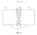
- FIG. 4is a simplified top diagram of an integrated electronic device according to an embodiment of the present invention.
- device 400includes a substrate 410 , one or more integrated micro electro-mechanical systems and electronic devices 420 , one or more trench structures 430 , a passivation layer 440 , a conduction layer 450 , and one or more edge bond pad structures.
- Device 400 shown in this figurecan represent an integrated electronic device following singulation, as referred to previously in FIG. 1 .
- Those skilled in the artwill recognize other variations, modifications, and alternatives.
- substrate 410can have a surface region.
- the substratecan be a buried oxide (BOX) substrate.
- the substratecan include an epitaxial (EPI) material.
- the substratecan have a silicon, single crystal silicon, or polycrystalline silicon material.
- one or more integrated micro electro-mechanical systems and electronic devices 420can be formed on a first region overlying the surface region. The first region can have a first surface region.
- one or more integrated micro electromechanical systems and electronic devices 420can include transistor devices, metal layers, via structures, and others. Integrated micro electro-mechanical systems and electronic devices 420 can also include a conduction material, a metal material, a metal alloy material, an insulating material, a dielectric material, or other materials or combinations thereof. Additionally, integrated micro electro-mechanical systems and electronic devices 420 can include integrated CMOS circuit devices, MEMS devices, anisotropic magnetic resonance (AMR) devices, or other devices or combinations thereof. In further embodiments, additional transistors, metal layers, and structures can be added.
- Each of integrated micro electro-mechanical systems and electronic devices 420can have one or more contact regions.
- Each of the contact regionscan include one or more bond pads, bonding structures, or conductive regions, as well as others.
- the fabrication of one or more integrated micro electro-mechanical systems and electronic devices 420can be done through foundry-compatible processes. Of course, there can be other variations, modifications, and alternatives.
- one or more trench structures 430can be formed within one or more portions of the first region.
- one or more trench structures 430can be formed from a wet etching, dry etching, or mechanical process.
- one or more trench structures 430can be formed from a deep reactive-ion etching (DRIE) process.
- DRIEdeep reactive-ion etching
- Device 400can also have an enclosure formed to house one or more integrated micro electro-mechanical systems and electronic devices 420 .
- the enclosurecan include a silicon material, an insulating material, or other material or combination thereof.
- passivation material 440can be formed overlying the first region one or more trench structures 430 , the enclosure, and one or more of the contact regions.
- passivation material 440can include an insulating material.
- the insulating materialcan include a dielectric material, or other material or combination thereof.
- One or more portions of passivation material 440can also be removed within a vicinity of one or more of the contact regions of integrated micro electro-mechanical systems and electronic devices 420 and one or more trench structures 430 .
- the removal process of passivation material 440can include a patterning process, or an etching process, or other processes. Again, there can be other variations, modifications, and alternatives.
- conduction material 450can include a metal material, a metal alloy, other conductive materials or combinations thereof. One or more portions of conduction material 450 can also be removed within a vicinity of one or more of the contact regions of integrated micro electro-mechanical systems and electronic devices 420 and one or more trench structures 430 to form one or more bond pad structures. In a specific embodiment, the removal process of conduction material 450 can include a patterning process, or an etching process, or other processes. Again, there can be other variations, modifications, and alternatives.
- the one or more edge bond padscan be operably coupled to the conduction material 450 and the passivation material 440 .
- the one or more edge bond pad structurescan be formed by a singulation process within a vicinity of the one or more bond pad structures.
- the singulation processcan include a dicing, an etching, or a laser scribing process.
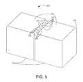
- FIG. 5is a simplified perspective diagram of an integrated electronic device according to an embodiment of the present invention.
- device 500includes a substrate 510 , one or more integrated micro electro-mechanical systems and electronic devices 520 , one or more trench structures 530 , a passivation layer 540 , a conduction layer 550 , and one or more edge bond pad structures.
- Device 500 shown in this figurecan represent an integrated electronic device following singulation, as referred to previously in FIG. 1 .
- a detailed description regarding the structure and the elements device 500can be found above in the description for FIG. 4 .
- Those skilled in the artwill recognize other variations, modifications, and alternatives.
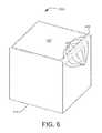
- FIG. 6is a simplified perspective diagram of an integrated electronic device according to an embodiment of the present invention.
- device 600includes a substrate 610 , one or more integrated micro electro-mechanical systems and electronic devices 620 , one or more trench structures 630 , a passivation layer 640 , a conduction layer 650 , and one or more edge bond pad structures.
- a detailed description regarding the structure and the elements device 600can be found above in the description for FIG. 4 .
- Features of this embodimentare shown more clearly in close-up 601 . Those skilled in the art will recognize other variations, modifications, and alternatives.
Landscapes
- Engineering & Computer Science (AREA)
- Microelectronics & Electronic Packaging (AREA)
- Manufacturing & Machinery (AREA)
- Computer Hardware Design (AREA)
- Power Engineering (AREA)
- Physics & Mathematics (AREA)
- Condensed Matter Physics & Semiconductors (AREA)
- General Physics & Mathematics (AREA)
- Micromachines (AREA)
Abstract
Description
Claims (10)
Priority Applications (1)
| Application Number | Priority Date | Filing Date | Title |
|---|---|---|---|
| US13/751,014US8592993B2 (en) | 2010-04-08 | 2013-01-25 | Method and structure of integrated micro electro-mechanical systems and electronic devices using edge bond pads |
Applications Claiming Priority (3)
| Application Number | Priority Date | Filing Date | Title |
|---|---|---|---|
| US32219810P | 2010-04-08 | 2010-04-08 | |
| US13/082,384US8367522B1 (en) | 2010-04-08 | 2011-04-07 | Method and structure of integrated micro electro-mechanical systems and electronic devices using edge bond pads |
| US13/751,014US8592993B2 (en) | 2010-04-08 | 2013-01-25 | Method and structure of integrated micro electro-mechanical systems and electronic devices using edge bond pads |
Related Parent Applications (1)
| Application Number | Title | Priority Date | Filing Date |
|---|---|---|---|
| US13/082,384DivisionUS8367522B1 (en) | 2010-04-08 | 2011-04-07 | Method and structure of integrated micro electro-mechanical systems and electronic devices using edge bond pads |
Publications (2)
| Publication Number | Publication Date |
|---|---|
| US20130134599A1 US20130134599A1 (en) | 2013-05-30 |
| US8592993B2true US8592993B2 (en) | 2013-11-26 |
Family
ID=47604563
Family Applications (2)
| Application Number | Title | Priority Date | Filing Date |
|---|---|---|---|
| US13/082,384Active - Reinstated2031-05-19US8367522B1 (en) | 2010-04-08 | 2011-04-07 | Method and structure of integrated micro electro-mechanical systems and electronic devices using edge bond pads |
| US13/751,014ActiveUS8592993B2 (en) | 2010-04-08 | 2013-01-25 | Method and structure of integrated micro electro-mechanical systems and electronic devices using edge bond pads |
Family Applications Before (1)
| Application Number | Title | Priority Date | Filing Date |
|---|---|---|---|
| US13/082,384Active - Reinstated2031-05-19US8367522B1 (en) | 2010-04-08 | 2011-04-07 | Method and structure of integrated micro electro-mechanical systems and electronic devices using edge bond pads |
Country Status (1)
| Country | Link |
|---|---|
| US (2) | US8367522B1 (en) |
Cited By (4)
| Publication number | Priority date | Publication date | Assignee | Title |
|---|---|---|---|---|
| US9423473B2 (en) | 2011-08-17 | 2016-08-23 | MCube Inc. | Three axis magnetic sensor device and method using flex cables |
| US9440846B2 (en) | 2009-10-28 | 2016-09-13 | Mcube, Inc. | System on a chip using integrated MEMS and CMOS devices |
| US9540232B2 (en) | 2010-11-12 | 2017-01-10 | MCube Inc. | Method and structure of MEMS WLCSP fabrication |
| US10913653B2 (en) | 2013-03-07 | 2021-02-09 | MCube Inc. | Method of fabricating MEMS devices using plasma etching and device therefor |
Families Citing this family (17)
| Publication number | Priority date | Publication date | Assignee | Title |
|---|---|---|---|---|
| US8797279B2 (en) | 2010-05-25 | 2014-08-05 | MCube Inc. | Analog touchscreen methods and apparatus |
| US8928602B1 (en) | 2009-03-03 | 2015-01-06 | MCube Inc. | Methods and apparatus for object tracking on a hand-held device |
| US8421082B1 (en) | 2010-01-19 | 2013-04-16 | Mcube, Inc. | Integrated CMOS and MEMS with air dielectric method and system |
| US8476129B1 (en) | 2010-05-24 | 2013-07-02 | MCube Inc. | Method and structure of sensors and MEMS devices using vertical mounting with interconnections |
| US8710597B1 (en) | 2010-04-21 | 2014-04-29 | MCube Inc. | Method and structure for adding mass with stress isolation to MEMS structures |
| US8477473B1 (en) | 2010-08-19 | 2013-07-02 | MCube Inc. | Transducer structure and method for MEMS devices |
| US8553389B1 (en) | 2010-08-19 | 2013-10-08 | MCube Inc. | Anchor design and method for MEMS transducer apparatuses |
| US9709509B1 (en) | 2009-11-13 | 2017-07-18 | MCube Inc. | System configured for integrated communication, MEMS, Processor, and applications using a foundry compatible semiconductor process |
| US8936959B1 (en) | 2010-02-27 | 2015-01-20 | MCube Inc. | Integrated rf MEMS, control systems and methods |
| US8794065B1 (en) | 2010-02-27 | 2014-08-05 | MCube Inc. | Integrated inertial sensing apparatus using MEMS and quartz configured on crystallographic planes |
| US8367522B1 (en) | 2010-04-08 | 2013-02-05 | MCube Inc. | Method and structure of integrated micro electro-mechanical systems and electronic devices using edge bond pads |
| US8928696B1 (en) | 2010-05-25 | 2015-01-06 | MCube Inc. | Methods and apparatus for operating hysteresis on a hand held device |
| US8869616B1 (en) | 2010-06-18 | 2014-10-28 | MCube Inc. | Method and structure of an inertial sensor using tilt conversion |
| US8652961B1 (en) | 2010-06-18 | 2014-02-18 | MCube Inc. | Methods and structure for adapting MEMS structures to form electrical interconnections for integrated circuits |
| US8993362B1 (en) | 2010-07-23 | 2015-03-31 | MCube Inc. | Oxide retainer method for MEMS devices |
| US8723986B1 (en) | 2010-11-04 | 2014-05-13 | MCube Inc. | Methods and apparatus for initiating image capture on a hand-held device |
| US10483239B2 (en)* | 2016-12-20 | 2019-11-19 | Sandisk Semiconductor (Shanghai) Co. Ltd. | Semiconductor device including dual pad wire bond interconnection |
Citations (149)
| Publication number | Priority date | Publication date | Assignee | Title |
|---|---|---|---|---|
| US3614677A (en) | 1966-04-29 | 1971-10-19 | Ibm | Electromechanical monolithic resonator |
| US4954698A (en) | 1985-01-14 | 1990-09-04 | Sumitomo Electric Industries, Ltd. | Sensor aligning means for optical reading apparatus |
| US5140745A (en)* | 1990-07-23 | 1992-08-25 | Mckenzie Jr Joseph A | Method for forming traces on side edges of printed circuit boards and devices formed thereby |
| US5157841A (en) | 1991-02-01 | 1992-10-27 | Dinsmore Robert C | Portable electronic compass |
| US5173597A (en) | 1990-11-23 | 1992-12-22 | Verifone, Inc. | Card reader with tapered card slot guide surface |
| US5488765A (en)* | 1992-07-27 | 1996-02-06 | Murata Manufacturing Co., Ltd. | Method of measuring characteristics of a multilayer electronic component |
| US5493769A (en) | 1993-08-05 | 1996-02-27 | Murata Manufacturing Co., Ltd. | Method of manufacturing electronic component and measuring characteristics of same |
| US5610414A (en) | 1993-07-28 | 1997-03-11 | Sharp Kabushiki Kaisha | Semiconductor device |
| US5668033A (en) | 1995-05-18 | 1997-09-16 | Nippondenso Co., Ltd. | Method for manufacturing a semiconductor acceleration sensor device |
| US5729074A (en) | 1994-03-24 | 1998-03-17 | Sumitomo Electric Industries, Ltd. | Micro mechanical component and production process thereof |
| US6046409A (en)* | 1997-02-26 | 2000-04-04 | Ngk Spark Plug Co., Ltd. | Multilayer microelectronic circuit |
| US6076731A (en) | 1997-04-10 | 2000-06-20 | Intermec Ip Corp. | Magnetic stripe reader with signature scanner |
| US6115261A (en) | 1999-06-14 | 2000-09-05 | Honeywell Inc. | Wedge mount for integrated circuit sensors |
| US6188322B1 (en) | 1999-09-28 | 2001-02-13 | Rockwell Technologies, Llc | Method for sensing electrical current |
| US6263736B1 (en) | 1999-09-24 | 2001-07-24 | Ut-Battelle, Llc | Electrostatically tunable resonance frequency beam utilizing a stress-sensitive film |
| US6278178B1 (en)* | 1998-02-10 | 2001-08-21 | Hyundai Electronics Industries Co., Ltd. | Integrated device package and fabrication methods thereof |
| US20010053565A1 (en) | 2000-06-19 | 2001-12-20 | Khoury Theodore A. | Method and apparatus for edge connection between elements of an integrated circuit |
| US20020072163A1 (en) | 2000-08-24 | 2002-06-13 | Ark-Chew Wong | Module and method of making same |
| US20020134837A1 (en) | 2001-01-23 | 2002-09-26 | Jakob Kishon | Method and apparatus for electronically exchanging data |
| US6480699B1 (en) | 1998-08-28 | 2002-11-12 | Woodtoga Holdings Company | Stand-alone device for transmitting a wireless signal containing data from a memory or a sensor |
| US6483172B1 (en) | 1998-03-09 | 2002-11-19 | Siemens Aktiengesellschaft | Semiconductor device structure with hydrogen-rich layer for facilitating passivation of surface states |
| US6485273B1 (en) | 2000-09-01 | 2002-11-26 | Mcnc | Distributed MEMS electrostatic pumping devices |
| US6534726B1 (en)* | 1999-10-25 | 2003-03-18 | Murata Manufacturing Co., Ltd. | Module substrate and method of producing the same |
| US20030058069A1 (en) | 2001-09-21 | 2003-03-27 | Schwartz Robert N. | Stress bimorph MEMS switches and methods of making same |
| US20030095115A1 (en) | 2001-11-22 | 2003-05-22 | Taylor Brian | Stylus input device utilizing a permanent magnet |
| US6576999B2 (en)* | 2000-07-06 | 2003-06-10 | Murata Manufacturing Co., Ltd. | Mounting structure for an electronic component having an external terminal electrode |
| US20030184189A1 (en) | 2002-03-29 | 2003-10-02 | Sinclair Michael J. | Electrostatic bimorph actuator |
| US20030230802A1 (en)* | 2002-06-18 | 2003-12-18 | Poo Chia Yong | Semiconductor devices and semiconductor device components with peripherally located, castellated contacts, assemblies and packages including such semiconductor devices or packages and associated methods |
| US20040002808A1 (en) | 2002-06-26 | 2004-01-01 | Mitsubishi Denki Kabushiki Kaisha | Vehicle engine control device |
| US20040017644A1 (en) | 2001-09-07 | 2004-01-29 | Mcnc | Overdrive structures for flexible electrostatic switch |
| US20040016995A1 (en) | 2002-07-25 | 2004-01-29 | Kuo Shun Meen | MEMS control chip integration |
| US20040056742A1 (en) | 2000-12-11 | 2004-03-25 | Dabbaj Rad H. | Electrostatic device |
| US20040063325A1 (en) | 2002-01-11 | 2004-04-01 | Masami Urano | Semiconductor device having MEMS |
| US20040104268A1 (en) | 2002-07-30 | 2004-06-03 | Bailey Kenneth Stephen | Plug in credit card reader module for wireless cellular phone verifications |
| US20040113246A1 (en) | 2000-02-16 | 2004-06-17 | Micron Technology, Inc. | Method of packaging at a wafer level |
| US6753664B2 (en) | 2001-03-22 | 2004-06-22 | Creo Products Inc. | Method for linearization of an actuator via force gradient modification |
| US20040119836A1 (en) | 1998-06-26 | 2004-06-24 | Takashi Kitaguchi | Apparatus and method for correction of a deviation of digital camera |
| US20040140962A1 (en) | 2003-01-21 | 2004-07-22 | Microsoft Corporation | Inertial sensors integration |
| US20040177045A1 (en) | 2001-04-17 | 2004-09-09 | Brown Kerry Dennis | Three-legacy mode payment card with parametric authentication and data input elements |
| US20040207035A1 (en) | 2003-04-15 | 2004-10-21 | Honeywell International Inc. | Semiconductor device and magneto-resistive sensor integration |
| US20040227201A1 (en) | 2003-05-13 | 2004-11-18 | Innovative Technology Licensing, Llc | Modules integrating MEMS devices with pre-processed electronic circuitry, and methods for fabricating such modules |
| US6855572B2 (en)* | 2002-08-28 | 2005-02-15 | Micron Technology, Inc. | Castellation wafer level packaging of integrated circuit chips |
| US20050074147A1 (en) | 2003-09-23 | 2005-04-07 | Ncr Corporation | Biometric system |
| US20050090038A1 (en)* | 2001-08-03 | 2005-04-28 | Wallace Robert F. | Card manufacturing technique and resulting card |
| US6912336B2 (en) | 2002-03-15 | 2005-06-28 | Nippon Telegraph And Telephone Corporation | Optical switch device |
| US20050174338A1 (en) | 2002-06-12 | 2005-08-11 | Ros Kiri Ing | Method for locating an impact on a surface and device therefor |
| US6933165B2 (en) | 2001-08-31 | 2005-08-23 | Superconductor Technologies, Inc. | Method of making an electrostatic actuator |
| US20050247787A1 (en) | 2002-02-12 | 2005-11-10 | Clay Von Mueller | Magnetic stripe reader with power management control for attachment to a PDA device |
| US20060049826A1 (en) | 2001-03-01 | 2006-03-09 | Onix Microsystems | Optical cross-connect system |
| US7019434B2 (en) | 2002-11-08 | 2006-03-28 | Iris Ao, Inc. | Deformable mirror method and apparatus including bimorph flexures and integrated drive |
| US20060081954A1 (en) | 2004-09-29 | 2006-04-20 | Nve Corporation | Magnetic particle flow detector |
| US20060141786A1 (en) | 2003-02-11 | 2006-06-29 | Koninklijke Philips Electronics N.V. | Method of manufacturing an electronic device and electronic device |
| US20060168832A1 (en) | 2004-10-07 | 2006-08-03 | Yamaha Corporation | Geomagnetic sensor and geomagnetic sensor correction method, temperature sensor and temperature sensor correction method, geomagnetism detection device |
| US7095226B2 (en) | 2003-12-04 | 2006-08-22 | Honeywell International, Inc. | Vertical die chip-on-board |
| US20060192465A1 (en) | 2004-03-12 | 2006-08-31 | Sri International, A California Corporation | Mechanical meta-materials |
| US20060208326A1 (en) | 2005-03-18 | 2006-09-21 | Nasiri Steven S | Method of fabrication of ai/ge bonding in a wafer packaging environment and a product produced therefrom |
| US20060211044A1 (en) | 2003-02-24 | 2006-09-21 | Green Lawrence R | Translucent solid matrix assay device dor microarray analysis |
| US20060238621A1 (en) | 2005-04-26 | 2006-10-26 | Mitsumasa Okubo | Image pickup apparatus |
| US20060243049A1 (en) | 2005-04-28 | 2006-11-02 | Fujitsu Media Devices Limited | Angular velocity sensor |
| US7145555B2 (en) | 2000-11-22 | 2006-12-05 | Cirque Corporation | Stylus input device utilizing a permanent magnet |
| US20060274399A1 (en) | 2005-06-01 | 2006-12-07 | Miradia Inc. | Method and device for fabricating a release structure to facilitate bonding of mirror devices onto a substrate |
| US7183630B1 (en)* | 2002-04-15 | 2007-02-27 | Amkor Technology, Inc. | Lead frame with plated end leads |
| US7195945B1 (en) | 2004-09-15 | 2007-03-27 | United States Of America As Represented By The Secretary Of The Army | Minimizing the effect of 1/ƒ noise with a MEMS flux concentrator |
| US20070132733A1 (en) | 2004-06-08 | 2007-06-14 | Pranil Ram | Computer Apparatus with added functionality |
| US20070152976A1 (en) | 2005-12-30 | 2007-07-05 | Microsoft Corporation | Unintentional touch rejection |
| US7253079B2 (en) | 2002-05-09 | 2007-08-07 | The Charles Stark Draper Laboratory, Inc. | Coplanar mounting member for a MEM sensor |
| US20070181962A1 (en) | 2006-01-20 | 2007-08-09 | Aaron Partridge | Wafer encapsulated microelectromechanical structure and method of manufacturing same |
| US7258009B2 (en) | 2004-01-27 | 2007-08-21 | Seiko Epson Corporation | Clock generating device, vibration type gyro sensor, navigation device, imaging device, and electronic apparatus |
| US20070200564A1 (en) | 2006-02-28 | 2007-08-30 | Mario Motz | Magnetic Field Sensor, Sensor Comprising Same and Method for Manufacturing Same |
| US20070281379A1 (en) | 2006-06-04 | 2007-12-06 | Stark Brian H | Microelectromechanical systems having stored charge and methods for fabricating and using same |
| US20080014682A1 (en) | 2003-10-24 | 2008-01-17 | Miradia Inc. | Method and system for sealing packages for optics |
| US20080066547A1 (en) | 2005-03-31 | 2008-03-20 | Fujitsu Media Devices Limited | Angular velocity sensor |
| US7370530B2 (en) | 2004-09-01 | 2008-05-13 | Honeywell International Inc. | Package for MEMS devices |
| US20080110259A1 (en) | 2004-10-07 | 2008-05-15 | Shoichi Takeno | Angular Velocity Sensor Unit And Angular Velocity Sensor Diagnosing Device |
| US20080119000A1 (en) | 2006-11-20 | 2008-05-22 | Richard Yeh | Monolithic IC and MEMS microfabrication process |
| US20080123242A1 (en) | 2006-11-28 | 2008-05-29 | Zhou Tiansheng | Monolithic capacitive transducer |
| US7402449B2 (en) | 2005-02-25 | 2008-07-22 | Hitachi, Ltd. | Integrated micro electro-mechanical system and manufacturing method thereof |
| US20080211043A1 (en) | 2007-03-02 | 2008-09-04 | Miradia Inc. | Method and system for flip chip packaging of micro-mirror devices |
| US20080211113A1 (en) | 2002-06-14 | 2008-09-04 | Micron Technology, Inc. | Wafer level packaging |
| US20080210007A1 (en) | 2007-01-23 | 2008-09-04 | Fujitsu Media Devices Limited | Angular velocity sensor |
| US20080277747A1 (en) | 2007-05-08 | 2008-11-13 | Nazir Ahmad | MEMS device support structure for sensor packaging |
| US7453269B2 (en) | 2004-05-11 | 2008-11-18 | Samsung Electronics Co., Ltd. | Magnetic MEMS sensor device |
| US7454705B2 (en) | 2000-03-02 | 2008-11-18 | Microsoft Corporation | Cluster-based visualization of user traffic on an internet site |
| US20080283991A1 (en) | 2007-05-14 | 2008-11-20 | Fraunhofer-Gesellschaft Zur Foerderung Der Angewandten Forschung E.V. | Housed active microstructures with direct contacting to a substrate |
| US20090007661A1 (en) | 2007-07-06 | 2009-01-08 | Invensense Inc. | Integrated Motion Processing Unit (MPU) With MEMS Inertial Sensing And Embedded Digital Electronics |
| US7498715B2 (en) | 2005-10-31 | 2009-03-03 | Xiao Yang | Method and structure for an out-of plane compliant micro actuator |
| US7511379B1 (en)* | 2006-03-23 | 2009-03-31 | National Semiconductor Corporation | Surface mountable direct chip attach device and method including integral integrated circuit |
| US7521783B2 (en) | 2004-06-12 | 2009-04-21 | Macronix International Co., Ltd. | Ultra thin image sensor package structure and method for fabrication |
| US20090108440A1 (en) | 2007-10-26 | 2009-04-30 | Infineon Technologies Ag | Semiconductor device |
| US20090115412A1 (en) | 2005-03-24 | 2009-05-07 | Alps Electric Co., Ltd. | Magnetic sensing device and electronic compass using the same |
| US7536909B2 (en) | 2006-01-20 | 2009-05-26 | Memsic, Inc. | Three-dimensional multi-chips and tri-axial sensors and methods of manufacturing the same |
| US20090153500A1 (en) | 2007-12-17 | 2009-06-18 | Samsung Electronics Co., Ltd. | Dual pointing device and method based on 3-D motion and touch sensors |
| US7585750B2 (en)* | 2007-05-04 | 2009-09-08 | Stats Chippac, Ltd. | Semiconductor package having through-hole via on saw streets formed with partial saw |
| US20090262074A1 (en) | 2007-01-05 | 2009-10-22 | Invensense Inc. | Controlling and accessing content using motion processing on mobile devices |
| US20090267906A1 (en) | 2008-04-25 | 2009-10-29 | Nokia Corporation | Touch sensitive apparatus |
| US20090321510A1 (en) | 2008-05-30 | 2009-12-31 | Ncr Corporation | Token communication |
| US20100044121A1 (en) | 2008-08-15 | 2010-02-25 | Simon Steven H | Sensors, algorithms and applications for a high dimensional touchpad |
| US20100071467A1 (en) | 2008-09-24 | 2010-03-25 | Invensense | Integrated multiaxis motion sensor |
| US20100075481A1 (en) | 2008-07-08 | 2010-03-25 | Xiao (Charles) Yang | Method and structure of monolithically integrated ic-mems oscillator using ic foundry-compatible processes |
| US7690255B2 (en) | 2006-08-31 | 2010-04-06 | Evigia Systems, Inc. | Three-axis inertial sensor and method of forming |
| US20100083756A1 (en) | 2007-04-05 | 2010-04-08 | Fraunhofer-Gesellschaft zur Foeerderung der angewa | Micromechanical Inertial Sensor for Measuring Rotation Rates |
| US7708189B1 (en) | 2002-05-17 | 2010-05-04 | Cipriano Joseph J | Identification verification system and method |
| US20100109102A1 (en) | 2005-01-03 | 2010-05-06 | Miradia Inc. | Method and structure for forming a gyroscope and accelerometer |
| US20100208118A1 (en) | 2009-02-17 | 2010-08-19 | Canon Kabushiki Kaisha | Image processing apparatus and method |
| US7779689B2 (en) | 2007-02-21 | 2010-08-24 | Freescale Semiconductor, Inc. | Multiple axis transducer with multiple sensing range capability |
| US20100236327A1 (en) | 2009-03-17 | 2010-09-23 | Minyao Mao | Tri-axis Angular Rate Sensor |
| US20100248662A1 (en) | 2009-03-25 | 2010-09-30 | Qualcomm Incorporated | Altitude-dependent power management |
| US20100260388A1 (en) | 2008-12-31 | 2010-10-14 | Peter Garrett | Hand-held Electronics Device for Aggregation of and Management of Personal Electronic Data |
| US7814791B2 (en) | 2004-10-20 | 2010-10-19 | Imego Ab | Sensor device |
| US7814792B2 (en) | 2007-01-26 | 2010-10-19 | Epson Toyocom Corporation | Gyro-module |
| US7814793B2 (en) | 2007-02-05 | 2010-10-19 | Epson Toyocom Corporation | Gyro sensor module and angular velocity detection method |
| US20100302199A1 (en) | 2009-05-26 | 2010-12-02 | Microsoft Corporation | Ferromagnetic user interfaces |
| US20100306117A1 (en) | 2009-05-29 | 2010-12-02 | Fujifilm Corporation | Construction inspection system, portable terminal, construction inspection method, program, and recording medium |
| US20100312519A1 (en) | 2009-06-03 | 2010-12-09 | Apple Inc. | Automatically identifying geographic direction |
| US20100307016A1 (en) | 2009-06-05 | 2010-12-09 | Apple Inc. | Magnetometer Accuracy and Use |
| US7861422B2 (en) | 2007-08-22 | 2011-01-04 | Solmetric Corporation | Skyline imaging system for solar access determination |
| US20110146401A1 (en) | 2009-12-22 | 2011-06-23 | Sony Corporation | Angular velocity sensor and electronic apparatus |
| US20110154905A1 (en) | 2009-12-25 | 2011-06-30 | Industrial Technology Research Institute | Capacitive sensor and manufacturing method thereof |
| US20110172918A1 (en) | 2010-01-13 | 2011-07-14 | Qualcomm Incorporated | Motion state detection for mobile device |
| US20110183456A1 (en) | 2010-01-22 | 2011-07-28 | Solid State System Co., Ltd. | Method for fabricating mems device |
| US20110198395A1 (en) | 2010-02-16 | 2011-08-18 | Mike Chen | Handheld mobile credit card reader |
| US8011577B2 (en) | 2007-12-24 | 2011-09-06 | Dynamics Inc. | Payment cards and devices with gift card, global integration, and magnetic stripe reader communication functionality |
| US8016191B2 (en) | 2004-07-01 | 2011-09-13 | American Express Travel Related Services Company, Inc. | Smartcard transaction system and method |
| US8037758B2 (en) | 2007-06-20 | 2011-10-18 | Seiko Epson Corporation | Angular velocity detection apparatus |
| US20110266340A9 (en) | 1998-04-17 | 2011-11-03 | James Block | Cash dispensing automated banking machine with flexible display |
| US20110265574A1 (en) | 2009-10-28 | 2011-11-03 | Mcube, Inc. | System on a Chip Using Integrated MEMS and CMOS Devices |
| US8056412B2 (en) | 2008-09-10 | 2011-11-15 | Rosemount Aerospace Inc. | Inertial measurement unit and method of constructing the same using two orthogonal surfaces |
| US20110312349A1 (en) | 2010-06-16 | 2011-12-22 | Qualcomm Incorporated | Layout design of proximity sensors to enable shortcuts |
| US8087296B2 (en) | 2006-03-15 | 2012-01-03 | Panasonic Corporation | Angular velocity sensor |
| US20120007598A1 (en) | 2010-07-09 | 2012-01-12 | Invensense, Inc. | Micromachined magnetic field sensors |
| US20120007597A1 (en) | 2010-07-09 | 2012-01-12 | Invensense, Inc. | Micromachined offset reduction structures for magnetic field sensing |
| US8148808B2 (en) | 2007-08-13 | 2012-04-03 | Lv Sensors, Inc. | Partitioning of electronic packages |
| US8181874B1 (en) | 2010-11-04 | 2012-05-22 | MCube Inc. | Methods and apparatus for facilitating capture of magnetic credit card data on a hand held device |
| US8227285B1 (en) | 2008-06-25 | 2012-07-24 | MCube Inc. | Method and structure of monolithetically integrated inertial sensor using IC foundry-compatible processes |
| US8236577B1 (en) | 2010-01-15 | 2012-08-07 | MCube Inc. | Foundry compatible process for manufacturing a magneto meter using lorentz force for integrated systems |
| US8245923B1 (en) | 2010-11-04 | 2012-08-21 | MCube Inc. | Methods and apparatus for capturing magnetic credit card data on a hand held device |
| US20120215475A1 (en) | 2010-08-20 | 2012-08-23 | Seektech, Inc. | Magnetic sensing user interface device methods and apparatus |
| US8259311B2 (en) | 2007-05-10 | 2012-09-04 | Leica Geosystems Ag | Method for determining position, laser beam detector and detector-reflector device for a system for determining position |
| US8324047B1 (en) | 2009-11-13 | 2012-12-04 | MCube Inc. | Method and structure of an integrated CMOS and MEMS device using air dielectric |
| US8342021B2 (en) | 2009-02-17 | 2013-01-01 | Seiko Epson Corporation | Composite sensor and electronic device |
| US8367522B1 (en) | 2010-04-08 | 2013-02-05 | MCube Inc. | Method and structure of integrated micro electro-mechanical systems and electronic devices using edge bond pads |
| US8395252B1 (en) | 2009-11-13 | 2013-03-12 | MCube Inc. | Integrated MEMS and CMOS package and method |
| US8402666B1 (en) | 2009-11-30 | 2013-03-26 | Mcube, Inc. | Magneto meter using lorentz force for integrated systems |
| US8407905B1 (en) | 2010-01-15 | 2013-04-02 | Mcube, Inc. | Multiple magneto meters using Lorentz force for integrated systems |
| US8421082B1 (en) | 2010-01-19 | 2013-04-16 | Mcube, Inc. | Integrated CMOS and MEMS with air dielectric method and system |
| US8477473B1 (en) | 2010-08-19 | 2013-07-02 | MCube Inc. | Transducer structure and method for MEMS devices |
| US8476084B1 (en) | 2010-05-24 | 2013-07-02 | MCube Inc. | Method and structure of sensors or electronic devices using vertical mounting |
| US8476129B1 (en) | 2010-05-24 | 2013-07-02 | MCube Inc. | Method and structure of sensors and MEMS devices using vertical mounting with interconnections |
| US8486723B1 (en) | 2010-08-19 | 2013-07-16 | MCube Inc. | Three axis magnetic sensor device and method |
- 2011
- 2011-04-07USUS13/082,384patent/US8367522B1/enactiveActive - Reinstated
- 2013
- 2013-01-25USUS13/751,014patent/US8592993B2/enactiveActive
Patent Citations (166)
| Publication number | Priority date | Publication date | Assignee | Title |
|---|---|---|---|---|
| US3614677A (en) | 1966-04-29 | 1971-10-19 | Ibm | Electromechanical monolithic resonator |
| US4954698A (en) | 1985-01-14 | 1990-09-04 | Sumitomo Electric Industries, Ltd. | Sensor aligning means for optical reading apparatus |
| US5140745A (en)* | 1990-07-23 | 1992-08-25 | Mckenzie Jr Joseph A | Method for forming traces on side edges of printed circuit boards and devices formed thereby |
| US5173597A (en) | 1990-11-23 | 1992-12-22 | Verifone, Inc. | Card reader with tapered card slot guide surface |
| US5157841A (en) | 1991-02-01 | 1992-10-27 | Dinsmore Robert C | Portable electronic compass |
| US5488765A (en)* | 1992-07-27 | 1996-02-06 | Murata Manufacturing Co., Ltd. | Method of measuring characteristics of a multilayer electronic component |
| US5610414A (en) | 1993-07-28 | 1997-03-11 | Sharp Kabushiki Kaisha | Semiconductor device |
| US5493769A (en) | 1993-08-05 | 1996-02-27 | Murata Manufacturing Co., Ltd. | Method of manufacturing electronic component and measuring characteristics of same |
| US5729074A (en) | 1994-03-24 | 1998-03-17 | Sumitomo Electric Industries, Ltd. | Micro mechanical component and production process thereof |
| US5668033A (en) | 1995-05-18 | 1997-09-16 | Nippondenso Co., Ltd. | Method for manufacturing a semiconductor acceleration sensor device |
| US6046409A (en)* | 1997-02-26 | 2000-04-04 | Ngk Spark Plug Co., Ltd. | Multilayer microelectronic circuit |
| US6076731A (en) | 1997-04-10 | 2000-06-20 | Intermec Ip Corp. | Magnetic stripe reader with signature scanner |
| US6278178B1 (en)* | 1998-02-10 | 2001-08-21 | Hyundai Electronics Industries Co., Ltd. | Integrated device package and fabrication methods thereof |
| US6483172B1 (en) | 1998-03-09 | 2002-11-19 | Siemens Aktiengesellschaft | Semiconductor device structure with hydrogen-rich layer for facilitating passivation of surface states |
| US20110266340A9 (en) | 1998-04-17 | 2011-11-03 | James Block | Cash dispensing automated banking machine with flexible display |
| US8070055B2 (en) | 1998-04-17 | 2011-12-06 | Diebold Self-Service Systems Division Of Diebold, Incorporated | Banking terminal that operates to cause financial transfers responsive to data bearing records |
| US20040119836A1 (en) | 1998-06-26 | 2004-06-24 | Takashi Kitaguchi | Apparatus and method for correction of a deviation of digital camera |
| US6480699B1 (en) | 1998-08-28 | 2002-11-12 | Woodtoga Holdings Company | Stand-alone device for transmitting a wireless signal containing data from a memory or a sensor |
| US6115261A (en) | 1999-06-14 | 2000-09-05 | Honeywell Inc. | Wedge mount for integrated circuit sensors |
| US6263736B1 (en) | 1999-09-24 | 2001-07-24 | Ut-Battelle, Llc | Electrostatically tunable resonance frequency beam utilizing a stress-sensitive film |
| US6188322B1 (en) | 1999-09-28 | 2001-02-13 | Rockwell Technologies, Llc | Method for sensing electrical current |
| US6534726B1 (en)* | 1999-10-25 | 2003-03-18 | Murata Manufacturing Co., Ltd. | Module substrate and method of producing the same |
| US20040113246A1 (en) | 2000-02-16 | 2004-06-17 | Micron Technology, Inc. | Method of packaging at a wafer level |
| US7454705B2 (en) | 2000-03-02 | 2008-11-18 | Microsoft Corporation | Cluster-based visualization of user traffic on an internet site |
| US20010053565A1 (en) | 2000-06-19 | 2001-12-20 | Khoury Theodore A. | Method and apparatus for edge connection between elements of an integrated circuit |
| US6576999B2 (en)* | 2000-07-06 | 2003-06-10 | Murata Manufacturing Co., Ltd. | Mounting structure for an electronic component having an external terminal electrode |
| US20020072163A1 (en) | 2000-08-24 | 2002-06-13 | Ark-Chew Wong | Module and method of making same |
| US6485273B1 (en) | 2000-09-01 | 2002-11-26 | Mcnc | Distributed MEMS electrostatic pumping devices |
| US7145555B2 (en) | 2000-11-22 | 2006-12-05 | Cirque Corporation | Stylus input device utilizing a permanent magnet |
| US20040056742A1 (en) | 2000-12-11 | 2004-03-25 | Dabbaj Rad H. | Electrostatic device |
| US20020134837A1 (en) | 2001-01-23 | 2002-09-26 | Jakob Kishon | Method and apparatus for electronically exchanging data |
| US20060049826A1 (en) | 2001-03-01 | 2006-03-09 | Onix Microsystems | Optical cross-connect system |
| US6753664B2 (en) | 2001-03-22 | 2004-06-22 | Creo Products Inc. | Method for linearization of an actuator via force gradient modification |
| US20040177045A1 (en) | 2001-04-17 | 2004-09-09 | Brown Kerry Dennis | Three-legacy mode payment card with parametric authentication and data input elements |
| US20050090038A1 (en)* | 2001-08-03 | 2005-04-28 | Wallace Robert F. | Card manufacturing technique and resulting card |
| US6933165B2 (en) | 2001-08-31 | 2005-08-23 | Superconductor Technologies, Inc. | Method of making an electrostatic actuator |
| US20040017644A1 (en) | 2001-09-07 | 2004-01-29 | Mcnc | Overdrive structures for flexible electrostatic switch |
| US20030058069A1 (en) | 2001-09-21 | 2003-03-27 | Schwartz Robert N. | Stress bimorph MEMS switches and methods of making same |
| US20030095115A1 (en) | 2001-11-22 | 2003-05-22 | Taylor Brian | Stylus input device utilizing a permanent magnet |
| US20040063325A1 (en) | 2002-01-11 | 2004-04-01 | Masami Urano | Semiconductor device having MEMS |
| US20050247787A1 (en) | 2002-02-12 | 2005-11-10 | Clay Von Mueller | Magnetic stripe reader with power management control for attachment to a PDA device |
| US7430674B2 (en) | 2002-02-12 | 2008-09-30 | Semtek Innovative Solutions, Inc. | Magnetic stripe reader with power management control for attachment to a PDA device |
| US6912336B2 (en) | 2002-03-15 | 2005-06-28 | Nippon Telegraph And Telephone Corporation | Optical switch device |
| US20030184189A1 (en) | 2002-03-29 | 2003-10-02 | Sinclair Michael J. | Electrostatic bimorph actuator |
| US7183630B1 (en)* | 2002-04-15 | 2007-02-27 | Amkor Technology, Inc. | Lead frame with plated end leads |
| US7253079B2 (en) | 2002-05-09 | 2007-08-07 | The Charles Stark Draper Laboratory, Inc. | Coplanar mounting member for a MEM sensor |
| US7708189B1 (en) | 2002-05-17 | 2010-05-04 | Cipriano Joseph J | Identification verification system and method |
| US20050174338A1 (en) | 2002-06-12 | 2005-08-11 | Ros Kiri Ing | Method for locating an impact on a surface and device therefor |
| US20080211113A1 (en) | 2002-06-14 | 2008-09-04 | Micron Technology, Inc. | Wafer level packaging |
| US20030230802A1 (en)* | 2002-06-18 | 2003-12-18 | Poo Chia Yong | Semiconductor devices and semiconductor device components with peripherally located, castellated contacts, assemblies and packages including such semiconductor devices or packages and associated methods |
| US20040002808A1 (en) | 2002-06-26 | 2004-01-01 | Mitsubishi Denki Kabushiki Kaisha | Vehicle engine control device |
| US20040016995A1 (en) | 2002-07-25 | 2004-01-29 | Kuo Shun Meen | MEMS control chip integration |
| US20040104268A1 (en) | 2002-07-30 | 2004-06-03 | Bailey Kenneth Stephen | Plug in credit card reader module for wireless cellular phone verifications |
| US7193312B2 (en)* | 2002-08-28 | 2007-03-20 | Micron Technology, Inc. | Castellation wafer level packaging of integrated circuit chips |
| US6855572B2 (en)* | 2002-08-28 | 2005-02-15 | Micron Technology, Inc. | Castellation wafer level packaging of integrated circuit chips |
| US7019434B2 (en) | 2002-11-08 | 2006-03-28 | Iris Ao, Inc. | Deformable mirror method and apparatus including bimorph flexures and integrated drive |
| US20040140962A1 (en) | 2003-01-21 | 2004-07-22 | Microsoft Corporation | Inertial sensors integration |
| US20060141786A1 (en) | 2003-02-11 | 2006-06-29 | Koninklijke Philips Electronics N.V. | Method of manufacturing an electronic device and electronic device |
| US20060211044A1 (en) | 2003-02-24 | 2006-09-21 | Green Lawrence R | Translucent solid matrix assay device dor microarray analysis |
| US20040207035A1 (en) | 2003-04-15 | 2004-10-21 | Honeywell International Inc. | Semiconductor device and magneto-resistive sensor integration |
| US7239000B2 (en) | 2003-04-15 | 2007-07-03 | Honeywell International Inc. | Semiconductor device and magneto-resistive sensor integration |
| US6979872B2 (en) | 2003-05-13 | 2005-12-27 | Rockwell Scientific Licensing, Llc | Modules integrating MEMS devices with pre-processed electronic circuitry, and methods for fabricating such modules |
| US20040227201A1 (en) | 2003-05-13 | 2004-11-18 | Innovative Technology Licensing, Llc | Modules integrating MEMS devices with pre-processed electronic circuitry, and methods for fabricating such modules |
| US20050074147A1 (en) | 2003-09-23 | 2005-04-07 | Ncr Corporation | Biometric system |
| US7493496B2 (en) | 2003-09-23 | 2009-02-17 | Ncr Corporation | Biometric system |
| US20080014682A1 (en) | 2003-10-24 | 2008-01-17 | Miradia Inc. | Method and system for sealing packages for optics |
| US7095226B2 (en) | 2003-12-04 | 2006-08-22 | Honeywell International, Inc. | Vertical die chip-on-board |
| US7258009B2 (en) | 2004-01-27 | 2007-08-21 | Seiko Epson Corporation | Clock generating device, vibration type gyro sensor, navigation device, imaging device, and electronic apparatus |
| US20060192465A1 (en) | 2004-03-12 | 2006-08-31 | Sri International, A California Corporation | Mechanical meta-materials |
| US7453269B2 (en) | 2004-05-11 | 2008-11-18 | Samsung Electronics Co., Ltd. | Magnetic MEMS sensor device |
| US20070132733A1 (en) | 2004-06-08 | 2007-06-14 | Pranil Ram | Computer Apparatus with added functionality |
| US7521783B2 (en) | 2004-06-12 | 2009-04-21 | Macronix International Co., Ltd. | Ultra thin image sensor package structure and method for fabrication |
| US8016191B2 (en) | 2004-07-01 | 2011-09-13 | American Express Travel Related Services Company, Inc. | Smartcard transaction system and method |
| US7370530B2 (en) | 2004-09-01 | 2008-05-13 | Honeywell International Inc. | Package for MEMS devices |
| US7195945B1 (en) | 2004-09-15 | 2007-03-27 | United States Of America As Represented By The Secretary Of The Army | Minimizing the effect of 1/ƒ noise with a MEMS flux concentrator |
| US20060081954A1 (en) | 2004-09-29 | 2006-04-20 | Nve Corporation | Magnetic particle flow detector |
| US7391091B2 (en) | 2004-09-29 | 2008-06-24 | Nve Corporation | Magnetic particle flow detector |
| US20080110259A1 (en) | 2004-10-07 | 2008-05-15 | Shoichi Takeno | Angular Velocity Sensor Unit And Angular Velocity Sensor Diagnosing Device |
| US7676340B2 (en) | 2004-10-07 | 2010-03-09 | Yamaha Corporation | Geomagnetic sensor and geomagnetic sensor correction method, temperature sensor and temperature sensor correction method, geomagnetism detection device |
| US20060168832A1 (en) | 2004-10-07 | 2006-08-03 | Yamaha Corporation | Geomagnetic sensor and geomagnetic sensor correction method, temperature sensor and temperature sensor correction method, geomagnetism detection device |
| US7814791B2 (en) | 2004-10-20 | 2010-10-19 | Imego Ab | Sensor device |
| US20100109102A1 (en) | 2005-01-03 | 2010-05-06 | Miradia Inc. | Method and structure for forming a gyroscope and accelerometer |
| US7402449B2 (en) | 2005-02-25 | 2008-07-22 | Hitachi, Ltd. | Integrated micro electro-mechanical system and manufacturing method thereof |
| US20090049911A1 (en) | 2005-02-25 | 2009-02-26 | Hitachi, Ltd. | Integrated micro electro-mechanical system and manufacturing method thereof |
| US20060208326A1 (en) | 2005-03-18 | 2006-09-21 | Nasiri Steven S | Method of fabrication of ai/ge bonding in a wafer packaging environment and a product produced therefrom |
| US20090115412A1 (en) | 2005-03-24 | 2009-05-07 | Alps Electric Co., Ltd. | Magnetic sensing device and electronic compass using the same |
| US20080066547A1 (en) | 2005-03-31 | 2008-03-20 | Fujitsu Media Devices Limited | Angular velocity sensor |
| US20060238621A1 (en) | 2005-04-26 | 2006-10-26 | Mitsumasa Okubo | Image pickup apparatus |
| US20060243049A1 (en) | 2005-04-28 | 2006-11-02 | Fujitsu Media Devices Limited | Angular velocity sensor |
| US20060274399A1 (en) | 2005-06-01 | 2006-12-07 | Miradia Inc. | Method and device for fabricating a release structure to facilitate bonding of mirror devices onto a substrate |
| US7498715B2 (en) | 2005-10-31 | 2009-03-03 | Xiao Yang | Method and structure for an out-of plane compliant micro actuator |
| US20070152976A1 (en) | 2005-12-30 | 2007-07-05 | Microsoft Corporation | Unintentional touch rejection |
| US7536909B2 (en) | 2006-01-20 | 2009-05-26 | Memsic, Inc. | Three-dimensional multi-chips and tri-axial sensors and methods of manufacturing the same |
| US20070181962A1 (en) | 2006-01-20 | 2007-08-09 | Aaron Partridge | Wafer encapsulated microelectromechanical structure and method of manufacturing same |
| US20070200564A1 (en) | 2006-02-28 | 2007-08-30 | Mario Motz | Magnetic Field Sensor, Sensor Comprising Same and Method for Manufacturing Same |
| US8087296B2 (en) | 2006-03-15 | 2012-01-03 | Panasonic Corporation | Angular velocity sensor |
| US7511379B1 (en)* | 2006-03-23 | 2009-03-31 | National Semiconductor Corporation | Surface mountable direct chip attach device and method including integral integrated circuit |
| US7713785B1 (en) | 2006-03-23 | 2010-05-11 | National Semiconductor Corporation | Surface mountable direct chip attach device and method including integral integrated circuit |
| US20070281379A1 (en) | 2006-06-04 | 2007-12-06 | Stark Brian H | Microelectromechanical systems having stored charge and methods for fabricating and using same |
| US7456042B2 (en) | 2006-06-04 | 2008-11-25 | Robert Bosch Gmbh | Microelectromechanical systems having stored charge and methods for fabricating and using same |
| US7690255B2 (en) | 2006-08-31 | 2010-04-06 | Evigia Systems, Inc. | Three-axis inertial sensor and method of forming |
| US20080119000A1 (en) | 2006-11-20 | 2008-05-22 | Richard Yeh | Monolithic IC and MEMS microfabrication process |
| US8165323B2 (en) | 2006-11-28 | 2012-04-24 | Zhou Tiansheng | Monolithic capacitive transducer |
| US20080123242A1 (en) | 2006-11-28 | 2008-05-29 | Zhou Tiansheng | Monolithic capacitive transducer |
| US20090262074A1 (en) | 2007-01-05 | 2009-10-22 | Invensense Inc. | Controlling and accessing content using motion processing on mobile devices |
| US20080210007A1 (en) | 2007-01-23 | 2008-09-04 | Fujitsu Media Devices Limited | Angular velocity sensor |
| US7814792B2 (en) | 2007-01-26 | 2010-10-19 | Epson Toyocom Corporation | Gyro-module |
| US7814793B2 (en) | 2007-02-05 | 2010-10-19 | Epson Toyocom Corporation | Gyro sensor module and angular velocity detection method |
| US7779689B2 (en) | 2007-02-21 | 2010-08-24 | Freescale Semiconductor, Inc. | Multiple axis transducer with multiple sensing range capability |
| US20080211043A1 (en) | 2007-03-02 | 2008-09-04 | Miradia Inc. | Method and system for flip chip packaging of micro-mirror devices |
| US20100083756A1 (en) | 2007-04-05 | 2010-04-08 | Fraunhofer-Gesellschaft zur Foeerderung der angewa | Micromechanical Inertial Sensor for Measuring Rotation Rates |
| US7585750B2 (en)* | 2007-05-04 | 2009-09-08 | Stats Chippac, Ltd. | Semiconductor package having through-hole via on saw streets formed with partial saw |
| US20080277747A1 (en) | 2007-05-08 | 2008-11-13 | Nazir Ahmad | MEMS device support structure for sensor packaging |
| US8259311B2 (en) | 2007-05-10 | 2012-09-04 | Leica Geosystems Ag | Method for determining position, laser beam detector and detector-reflector device for a system for determining position |
| US20080283991A1 (en) | 2007-05-14 | 2008-11-20 | Fraunhofer-Gesellschaft Zur Foerderung Der Angewandten Forschung E.V. | Housed active microstructures with direct contacting to a substrate |
| US8037758B2 (en) | 2007-06-20 | 2011-10-18 | Seiko Epson Corporation | Angular velocity detection apparatus |
| US20090007661A1 (en) | 2007-07-06 | 2009-01-08 | Invensense Inc. | Integrated Motion Processing Unit (MPU) With MEMS Inertial Sensing And Embedded Digital Electronics |
| US8250921B2 (en) | 2007-07-06 | 2012-08-28 | Invensense, Inc. | Integrated motion processing unit (MPU) with MEMS inertial sensing and embedded digital electronics |
| US8148808B2 (en) | 2007-08-13 | 2012-04-03 | Lv Sensors, Inc. | Partitioning of electronic packages |
| US7861422B2 (en) | 2007-08-22 | 2011-01-04 | Solmetric Corporation | Skyline imaging system for solar access determination |
| US20090108440A1 (en) | 2007-10-26 | 2009-04-30 | Infineon Technologies Ag | Semiconductor device |
| US20090153500A1 (en) | 2007-12-17 | 2009-06-18 | Samsung Electronics Co., Ltd. | Dual pointing device and method based on 3-D motion and touch sensors |
| US8011577B2 (en) | 2007-12-24 | 2011-09-06 | Dynamics Inc. | Payment cards and devices with gift card, global integration, and magnetic stripe reader communication functionality |
| US20090267906A1 (en) | 2008-04-25 | 2009-10-29 | Nokia Corporation | Touch sensitive apparatus |
| US20090321510A1 (en) | 2008-05-30 | 2009-12-31 | Ncr Corporation | Token communication |
| US8227285B1 (en) | 2008-06-25 | 2012-07-24 | MCube Inc. | Method and structure of monolithetically integrated inertial sensor using IC foundry-compatible processes |
| US20100075481A1 (en) | 2008-07-08 | 2010-03-25 | Xiao (Charles) Yang | Method and structure of monolithically integrated ic-mems oscillator using ic foundry-compatible processes |
| US20100044121A1 (en) | 2008-08-15 | 2010-02-25 | Simon Steven H | Sensors, algorithms and applications for a high dimensional touchpad |
| US8056412B2 (en) | 2008-09-10 | 2011-11-15 | Rosemount Aerospace Inc. | Inertial measurement unit and method of constructing the same using two orthogonal surfaces |
| US20100071467A1 (en) | 2008-09-24 | 2010-03-25 | Invensense | Integrated multiaxis motion sensor |
| US20100260388A1 (en) | 2008-12-31 | 2010-10-14 | Peter Garrett | Hand-held Electronics Device for Aggregation of and Management of Personal Electronic Data |
| US8342021B2 (en) | 2009-02-17 | 2013-01-01 | Seiko Epson Corporation | Composite sensor and electronic device |
| US20100208118A1 (en) | 2009-02-17 | 2010-08-19 | Canon Kabushiki Kaisha | Image processing apparatus and method |
| US20100236327A1 (en) | 2009-03-17 | 2010-09-23 | Minyao Mao | Tri-axis Angular Rate Sensor |
| US20100248662A1 (en) | 2009-03-25 | 2010-09-30 | Qualcomm Incorporated | Altitude-dependent power management |
| US20100302199A1 (en) | 2009-05-26 | 2010-12-02 | Microsoft Corporation | Ferromagnetic user interfaces |
| US20100306117A1 (en) | 2009-05-29 | 2010-12-02 | Fujifilm Corporation | Construction inspection system, portable terminal, construction inspection method, program, and recording medium |
| US20100312519A1 (en) | 2009-06-03 | 2010-12-09 | Apple Inc. | Automatically identifying geographic direction |
| US20110131825A1 (en) | 2009-06-05 | 2011-06-09 | Apple Inc. | Magnetometer Accuracy and Use |
| US8061049B2 (en) | 2009-06-05 | 2011-11-22 | Apple Inc. | Magnetometer accuracy and use |
| US7891103B2 (en) | 2009-06-05 | 2011-02-22 | Apple Inc. | Magnetometer accuracy and use |
| US20100307016A1 (en) | 2009-06-05 | 2010-12-09 | Apple Inc. | Magnetometer Accuracy and Use |
| US20110265574A1 (en) | 2009-10-28 | 2011-11-03 | Mcube, Inc. | System on a Chip Using Integrated MEMS and CMOS Devices |
| US8395252B1 (en) | 2009-11-13 | 2013-03-12 | MCube Inc. | Integrated MEMS and CMOS package and method |
| US8324047B1 (en) | 2009-11-13 | 2012-12-04 | MCube Inc. | Method and structure of an integrated CMOS and MEMS device using air dielectric |
| US8402666B1 (en) | 2009-11-30 | 2013-03-26 | Mcube, Inc. | Magneto meter using lorentz force for integrated systems |
| US20110146401A1 (en) | 2009-12-22 | 2011-06-23 | Sony Corporation | Angular velocity sensor and electronic apparatus |
| US20110154905A1 (en) | 2009-12-25 | 2011-06-30 | Industrial Technology Research Institute | Capacitive sensor and manufacturing method thereof |
| US20110172918A1 (en) | 2010-01-13 | 2011-07-14 | Qualcomm Incorporated | Motion state detection for mobile device |
| US8407905B1 (en) | 2010-01-15 | 2013-04-02 | Mcube, Inc. | Multiple magneto meters using Lorentz force for integrated systems |
| US8236577B1 (en) | 2010-01-15 | 2012-08-07 | MCube Inc. | Foundry compatible process for manufacturing a magneto meter using lorentz force for integrated systems |
| US8421082B1 (en) | 2010-01-19 | 2013-04-16 | Mcube, Inc. | Integrated CMOS and MEMS with air dielectric method and system |
| US20110183456A1 (en) | 2010-01-22 | 2011-07-28 | Solid State System Co., Ltd. | Method for fabricating mems device |
| US20110198395A1 (en) | 2010-02-16 | 2011-08-18 | Mike Chen | Handheld mobile credit card reader |
| US8367522B1 (en) | 2010-04-08 | 2013-02-05 | MCube Inc. | Method and structure of integrated micro electro-mechanical systems and electronic devices using edge bond pads |
| US8476084B1 (en) | 2010-05-24 | 2013-07-02 | MCube Inc. | Method and structure of sensors or electronic devices using vertical mounting |
| US8476129B1 (en) | 2010-05-24 | 2013-07-02 | MCube Inc. | Method and structure of sensors and MEMS devices using vertical mounting with interconnections |
| US20110312349A1 (en) | 2010-06-16 | 2011-12-22 | Qualcomm Incorporated | Layout design of proximity sensors to enable shortcuts |
| US20120007598A1 (en) | 2010-07-09 | 2012-01-12 | Invensense, Inc. | Micromachined magnetic field sensors |
| US8395381B2 (en) | 2010-07-09 | 2013-03-12 | Invensense, Inc. | Micromachined magnetic field sensors |
| US20120007597A1 (en) | 2010-07-09 | 2012-01-12 | Invensense, Inc. | Micromachined offset reduction structures for magnetic field sensing |
| US8477473B1 (en) | 2010-08-19 | 2013-07-02 | MCube Inc. | Transducer structure and method for MEMS devices |
| US8486723B1 (en) | 2010-08-19 | 2013-07-16 | MCube Inc. | Three axis magnetic sensor device and method |
| US20120215475A1 (en) | 2010-08-20 | 2012-08-23 | Seektech, Inc. | Magnetic sensing user interface device methods and apparatus |
| US8245923B1 (en) | 2010-11-04 | 2012-08-21 | MCube Inc. | Methods and apparatus for capturing magnetic credit card data on a hand held device |
| US8181874B1 (en) | 2010-11-04 | 2012-05-22 | MCube Inc. | Methods and apparatus for facilitating capture of magnetic credit card data on a hand held device |
Cited By (4)
| Publication number | Priority date | Publication date | Assignee | Title |
|---|---|---|---|---|
| US9440846B2 (en) | 2009-10-28 | 2016-09-13 | Mcube, Inc. | System on a chip using integrated MEMS and CMOS devices |
| US9540232B2 (en) | 2010-11-12 | 2017-01-10 | MCube Inc. | Method and structure of MEMS WLCSP fabrication |
| US9423473B2 (en) | 2011-08-17 | 2016-08-23 | MCube Inc. | Three axis magnetic sensor device and method using flex cables |
| US10913653B2 (en) | 2013-03-07 | 2021-02-09 | MCube Inc. | Method of fabricating MEMS devices using plasma etching and device therefor |
Also Published As
| Publication number | Publication date |
|---|---|
| US8367522B1 (en) | 2013-02-05 |
| US20130134599A1 (en) | 2013-05-30 |
Similar Documents
| Publication | Publication Date | Title |
|---|---|---|
| US8592993B2 (en) | Method and structure of integrated micro electro-mechanical systems and electronic devices using edge bond pads | |
| US8421082B1 (en) | Integrated CMOS and MEMS with air dielectric method and system | |
| US8794065B1 (en) | Integrated inertial sensing apparatus using MEMS and quartz configured on crystallographic planes | |
| US8476084B1 (en) | Method and structure of sensors or electronic devices using vertical mounting | |
| US10046964B2 (en) | MEMS structure with improved shielding and method | |
| US9150406B2 (en) | Multi-axis integrated MEMS devices with CMOS circuits and method therefor | |
| US9440846B2 (en) | System on a chip using integrated MEMS and CMOS devices | |
| US8742520B2 (en) | Three axis magnetic sensor device and method | |
| US8476129B1 (en) | Method and structure of sensors and MEMS devices using vertical mounting with interconnections | |
| US9340414B2 (en) | Method and structure of monolithically integrated absolute pressure sensor | |
| US10155655B2 (en) | MEMS devices and fabrication methods thereof | |
| US8936959B1 (en) | Integrated rf MEMS, control systems and methods | |
| KR102257709B1 (en) | Methods of forming buried microelectricomechanical structures coupled with device substrates and structures formed thereby | |
| US8969101B1 (en) | Three axis magnetic sensor device and method using flex cables | |
| US9725298B2 (en) | CMOS integrated moving-gate transducer with silicon as a functional layer | |
| US8129805B2 (en) | Microelectromechanical system (MEMS) device and methods for fabricating the same | |
| US8993362B1 (en) | Oxide retainer method for MEMS devices | |
| US8584521B1 (en) | Accurate gyroscope device using MEMS and quartz | |
| US10913653B2 (en) | Method of fabricating MEMS devices using plasma etching and device therefor | |
| US9321629B2 (en) | Method and structure for adding mass with stress isolation to MEMS structures | |
| US8564075B1 (en) | Package tolerate design and method | |
| Cheng et al. | Bulk-Si with poly bump process scheme for MEMS sensors | |
| US9738510B1 (en) | Method and structure of MEMS PLCSP fabrication | |
| TW201227873A (en) | Method for manufacturing a micro-electromechanical structure |
Legal Events
| Date | Code | Title | Description |
|---|---|---|---|
| STCF | Information on status: patent grant | Free format text:PATENTED CASE | |
| FPAY | Fee payment | Year of fee payment:4 | |
| AS | Assignment | Owner name:SILICON VALLEY BANK, CALIFORNIA Free format text:SECURITY INTEREST;ASSIGNOR:MCUBE, INC.;REEL/FRAME:052909/0119 Effective date:20200608 | |
| AS | Assignment | Owner name:EASTWARD FUND MANAGEMENT, LLC, MASSACHUSETTS Free format text:SECURITY INTEREST;ASSIGNOR:MCUBE, INC.;REEL/FRAME:053826/0626 Effective date:20200608 | |
| MAFP | Maintenance fee payment | Free format text:PAYMENT OF MAINTENANCE FEE, 8TH YR, SMALL ENTITY (ORIGINAL EVENT CODE: M2552); ENTITY STATUS OF PATENT OWNER: SMALL ENTITY Year of fee payment:8 | |
| AS | Assignment | Owner name:EASTWARD FUND MANAGEMENT, LLC, MASSACHUSETTS Free format text:SECURITY INTEREST;ASSIGNOR:MOVELLA INC.;REEL/FRAME:058520/0690 Effective date:20211210 | |
| AS | Assignment | Owner name:MOVELLA INC., CALIFORNIA Free format text:CHANGE OF NAME;ASSIGNOR:MCUBE, INC.;REEL/FRAME:061602/0371 Effective date:20221031 | |
| AS | Assignment | Owner name:MOVELLA INC. (FORMERLY KNOWN AS MCUBE, INC.), CALIFORNIA Free format text:RELEASE BY SECURED PARTY;ASSIGNOR:SILICON VALLEY BANK;REEL/FRAME:061936/0024 Effective date:20221114 | |
| AS | Assignment | Owner name:WILMINGTON SAVINGS FUND SOCIETY, FSB, AS AGENT, DELAWARE Free format text:NOTICE OF GRANT OF SECURITY INTEREST IN PATENTS;ASSIGNOR:MOVELLA INC.;REEL/FRAME:061948/0764 Effective date:20221114 Owner name:MOVELLA INC. (FORMERLY KNOWN AS MCUBE, INC.), CALIFORNIA Free format text:RELEASE BY SECURED PARTY;ASSIGNOR:EASTWARD FUND MANAGEMENT, LLC;REEL/FRAME:061940/0635 Effective date:20221114 Owner name:MOVELLA INC., CALIFORNIA Free format text:RELEASE BY SECURED PARTY;ASSIGNOR:EASTWARD FUND MANAGEMENT, LLC;REEL/FRAME:061940/0602 Effective date:20221114 | |
| MAFP | Maintenance fee payment | Free format text:PAYMENT OF MAINTENANCE FEE, 12TH YR, SMALL ENTITY (ORIGINAL EVENT CODE: M2553); ENTITY STATUS OF PATENT OWNER: SMALL ENTITY Year of fee payment:12 |