US8592964B2 - Apparatus and method for high density multi-chip structures - Google Patents
Apparatus and method for high density multi-chip structuresDownload PDFInfo
- Publication number
- US8592964B2 US8592964B2US11/458,859US45885906AUS8592964B2US 8592964 B2US8592964 B2US 8592964B2US 45885906 AUS45885906 AUS 45885906AUS 8592964 B2US8592964 B2US 8592964B2
- Authority
- US
- United States
- Prior art keywords
- chip
- chips
- handling system
- information handling
- connection structures
- Prior art date
- Legal status (The legal status is an assumption and is not a legal conclusion. Google has not performed a legal analysis and makes no representation as to the accuracy of the status listed.)
- Expired - Lifetime, expires
Links
Images


Classifications
- H—ELECTRICITY
- H01—ELECTRIC ELEMENTS
- H01L—SEMICONDUCTOR DEVICES NOT COVERED BY CLASS H10
- H01L23/00—Details of semiconductor or other solid state devices
- H01L23/52—Arrangements for conducting electric current within the device in operation from one component to another, i.e. interconnections, e.g. wires, lead frames
- H01L23/522—Arrangements for conducting electric current within the device in operation from one component to another, i.e. interconnections, e.g. wires, lead frames including external interconnections consisting of a multilayer structure of conductive and insulating layers inseparably formed on the semiconductor body
- H01L23/5226—Via connections in a multilevel interconnection structure
- H—ELECTRICITY
- H01—ELECTRIC ELEMENTS
- H01L—SEMICONDUCTOR DEVICES NOT COVERED BY CLASS H10
- H01L25/00—Assemblies consisting of a plurality of semiconductor or other solid state devices
- H01L25/03—Assemblies consisting of a plurality of semiconductor or other solid state devices all the devices being of a type provided for in a single subclass of subclasses H10B, H10D, H10F, H10H, H10K or H10N, e.g. assemblies of rectifier diodes
- H01L25/04—Assemblies consisting of a plurality of semiconductor or other solid state devices all the devices being of a type provided for in a single subclass of subclasses H10B, H10D, H10F, H10H, H10K or H10N, e.g. assemblies of rectifier diodes the devices not having separate containers
- H01L25/065—Assemblies consisting of a plurality of semiconductor or other solid state devices all the devices being of a type provided for in a single subclass of subclasses H10B, H10D, H10F, H10H, H10K or H10N, e.g. assemblies of rectifier diodes the devices not having separate containers the devices being of a type provided for in group H10D89/00
- H01L25/0652—Assemblies consisting of a plurality of semiconductor or other solid state devices all the devices being of a type provided for in a single subclass of subclasses H10B, H10D, H10F, H10H, H10K or H10N, e.g. assemblies of rectifier diodes the devices not having separate containers the devices being of a type provided for in group H10D89/00 the devices being arranged next and on each other, i.e. mixed assemblies
- H—ELECTRICITY
- H01—ELECTRIC ELEMENTS
- H01L—SEMICONDUCTOR DEVICES NOT COVERED BY CLASS H10
- H01L25/00—Assemblies consisting of a plurality of semiconductor or other solid state devices
- H01L25/03—Assemblies consisting of a plurality of semiconductor or other solid state devices all the devices being of a type provided for in a single subclass of subclasses H10B, H10D, H10F, H10H, H10K or H10N, e.g. assemblies of rectifier diodes
- H01L25/04—Assemblies consisting of a plurality of semiconductor or other solid state devices all the devices being of a type provided for in a single subclass of subclasses H10B, H10D, H10F, H10H, H10K or H10N, e.g. assemblies of rectifier diodes the devices not having separate containers
- H01L25/065—Assemblies consisting of a plurality of semiconductor or other solid state devices all the devices being of a type provided for in a single subclass of subclasses H10B, H10D, H10F, H10H, H10K or H10N, e.g. assemblies of rectifier diodes the devices not having separate containers the devices being of a type provided for in group H10D89/00
- H01L25/0657—Stacked arrangements of devices
- H—ELECTRICITY
- H01—ELECTRIC ELEMENTS
- H01L—SEMICONDUCTOR DEVICES NOT COVERED BY CLASS H10
- H01L25/00—Assemblies consisting of a plurality of semiconductor or other solid state devices
- H01L25/18—Assemblies consisting of a plurality of semiconductor or other solid state devices the devices being of the types provided for in two or more different main groups of the same subclass of H10B, H10D, H10F, H10H, H10K or H10N
- H—ELECTRICITY
- H01—ELECTRIC ELEMENTS
- H01L—SEMICONDUCTOR DEVICES NOT COVERED BY CLASS H10
- H01L2225/00—Details relating to assemblies covered by the group H01L25/00 but not provided for in its subgroups
- H01L2225/03—All the devices being of a type provided for in the same main group of the same subclass of class H10, e.g. assemblies of rectifier diodes
- H01L2225/04—All the devices being of a type provided for in the same main group of the same subclass of class H10, e.g. assemblies of rectifier diodes the devices not having separate containers
- H01L2225/065—All the devices being of a type provided for in the same main group of the same subclass of class H10
- H01L2225/06503—Stacked arrangements of devices
- H01L2225/06524—Electrical connections formed on device or on substrate, e.g. a deposited or grown layer
- H—ELECTRICITY
- H01—ELECTRIC ELEMENTS
- H01L—SEMICONDUCTOR DEVICES NOT COVERED BY CLASS H10
- H01L2225/00—Details relating to assemblies covered by the group H01L25/00 but not provided for in its subgroups
- H01L2225/03—All the devices being of a type provided for in the same main group of the same subclass of class H10, e.g. assemblies of rectifier diodes
- H01L2225/04—All the devices being of a type provided for in the same main group of the same subclass of class H10, e.g. assemblies of rectifier diodes the devices not having separate containers
- H01L2225/065—All the devices being of a type provided for in the same main group of the same subclass of class H10
- H01L2225/06503—Stacked arrangements of devices
- H01L2225/06527—Special adaptation of electrical connections, e.g. rewiring, engineering changes, pressure contacts, layout
- H—ELECTRICITY
- H01—ELECTRIC ELEMENTS
- H01L—SEMICONDUCTOR DEVICES NOT COVERED BY CLASS H10
- H01L2225/00—Details relating to assemblies covered by the group H01L25/00 but not provided for in its subgroups
- H01L2225/03—All the devices being of a type provided for in the same main group of the same subclass of class H10, e.g. assemblies of rectifier diodes
- H01L2225/04—All the devices being of a type provided for in the same main group of the same subclass of class H10, e.g. assemblies of rectifier diodes the devices not having separate containers
- H01L2225/065—All the devices being of a type provided for in the same main group of the same subclass of class H10
- H01L2225/06503—Stacked arrangements of devices
- H01L2225/06551—Conductive connections on the side of the device
- H—ELECTRICITY
- H01—ELECTRIC ELEMENTS
- H01L—SEMICONDUCTOR DEVICES NOT COVERED BY CLASS H10
- H01L2924/00—Indexing scheme for arrangements or methods for connecting or disconnecting semiconductor or solid-state bodies as covered by H01L24/00
- H01L2924/0001—Technical content checked by a classifier
- H01L2924/0002—Not covered by any one of groups H01L24/00, H01L24/00 and H01L2224/00
Definitions
- This inventionrelates to semiconductor chips and chip assemblies. Specifically, this invention relates to multi-chip structures and methods of forming multi-chip structures.
- the capacitive coupling between adjacent metal linesbecomes a significant impediment to achieving higher performance.
- the minimum feature sizedecreases the number of devices potentially achievable in a given area increases, as a second power function.
- the number of wiring connectionsis increasing at least as rapidly. In order to accommodate the increased wiring, the chip designer would like to shrink the space between adjacent lines to the minimum achievable dimension. This has the unfortunate effect of increasing the capacitive load.
- One way to accommodate the increased wiring and reduce capacitive loadis to substitute lower dielectric constant materials for the insulating material.
- a common insulating material to dateis SiO 2 , which has a dielectric constant of around 4, is now used in most very large scale integrated circuit (VLSI) chips.
- Another way to accommodate the increased wiring and reduce capacitive loadis to shorten the distance between devices by more dense packaging.
- What is neededis a device design and method that improves the performance and reduces the size of a multi-chip assembly. Specifically, devices and methods are needed that utilize improved insulating materials. Further, devices and methods are needed that utilize improved dense packaging configurations.
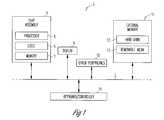
- FIG. 1illustrates an information handling system according to an embodiment of the invention.
- FIG. 2Aillustrates a chip in a stage of manufacture according to an embodiment of the invention.
- FIG. 2Billustrates a chip in a stage of manufacture according to an embodiment of the invention.
- FIG. 2Cillustrates a chip in a stage of manufacture according to an embodiment of the invention.
- FIG. 2Dillustrates a chip in a stage of manufacture according to an embodiment of the invention.
- FIG. 2Eillustrates a chip in a stage of manufacture according to an embodiment of the invention.
- FIG. 2Fillustrates a chip in a stage of manufacture according to an embodiment of the invention.
- FIG. 2Gillustrates a chip and carrier in a stage of manufacture according to an embodiment of the invention.
- FIG. 2Hillustrates a chip and carrier in a stage of manufacture according to an embodiment of the invention.
- FIG. 2Iillustrates a chip in a stage of manufacture according to an embodiment of the invention.
- FIG. 2Jillustrates a top view of a chip in a stage of manufacture according to an embodiment of the invention.
- FIG. 3illustrates a multi-chip assembly according to an embodiment of the invention.
- FIG. 4illustrates another multi-chip assembly according to an embodiment of the invention.
- wafer and substrate used in the following descriptioninclude any structure having an exposed surface with which to form the integrated circuit (IC) structure of the invention.
- substrateis understood to include semiconductor wafers.
- substrateis also used to refer to semiconductor structures during processing, and may include other layers, such as silicon-on-insulator (SOI), etc. that have been fabricated thereupon.
- SOIsilicon-on-insulator
- Both wafer and substrateinclude doped and undoped semiconductors, epitaxial semiconductor layers supported by a base semiconductor or insulator, as well as other semiconductor structures well known to one skilled in the art.
- conductoris understood to include semiconductors, and the term insulator or dielectric is defined to include any material that is less electrically conductive than the materials referred to as conductors.
- horizontalas used in this application is defined as a plane parallel to the conventional plane or surface of a wafer or substrate, regardless of the orientation of the wafer or substrate.
- verticalrefers to a direction perpendicular to the horizontal as defined above. Prepositions, such as “on”, “side” (as in “sidewall”), “higher”, “lower”, “over” and “under” are defined with respect to the conventional plane or surface being on the top surface of the wafer or substrate, regardless of the orientation of the wafer or substrate.
- a chipmay include both memory circuitry and logic circuitry on the same chip.
- a chip with both memory circuitry and logic circuitry on the same chipis defined to be both a “memory chip” and a “logic chip” as used in the following description.
- FIG. 1is a block diagram of an information handling system 1 incorporating at least one multi-chip assembly 4 in accordance with one embodiment of the invention.
- Information handling system 1is merely one example of an electronic system in which the present invention can be used.
- Other examplesinclude, but are not limited to personal data assistants (PDA's), cellular telephones, aircraft, satellites, military vehicles, etc.
- PDA'spersonal data assistants
- cellular telephonesaircraft, satellites, military vehicles, etc.
- information handling system 1comprises a data processing system that includes a system bus 2 to couple the various components of the system.
- System bus 2provides communications links among the various components of the information handling system 1 and can be implemented as a single bus, as a combination of busses, or in any other suitable manner.
- Multi-chip assembly 4is coupled to the system bus 2 .
- Multi-chip assembly 4can include any circuit or combination of circuits.
- multi-chip assembly 4includes a processor 6 which can be of any type.
- processormeans any type of computational circuit, such as but not limited to a microprocessor, a microcontroller, a graphics processor, a digital signal processor (DSP), or any other type of processor or processing circuit.
- a memory chip 7is included in the multi-chip assembly 4 .
- CMOScomplementary metal-oxide-semiconductor
- DRAMsDynamic Random Access Memory
- SRAMsStatic Random Access Memory
- VRAMsVRAMs and EEPROMs
- additional logic chips 8 other than processor chipsare included in the multi-chip assembly 4 .
- An example of a logic chip 8 other than a processorincludes an analog to digital converter.
- Other circuits on logic chips 8such as custom circuits, an application-specific integrated circuit (ASIC), etc. are also included in one embodiment of the invention.
- Information handling system 1can also include an external memory 11 , which in turn can include one or more memory elements suitable to the particular application, such as one or more hard drives 12 , and/or one or more drives that handle removable media 13 such as floppy diskettes, compact disks (CDs), digital video disks (DVDs), and the like.
- an external memory 11can include one or more memory elements suitable to the particular application, such as one or more hard drives 12 , and/or one or more drives that handle removable media 13 such as floppy diskettes, compact disks (CDs), digital video disks (DVDs), and the like.
- Information handling system 1can also include a display device 9 such as a monitor, additional peripheral components 10 , such as speakers, etc. and a keyboard and/or controller 14 , which can include a mouse, trackball, game controller, voice-recognition device, or any other device that permits a system user to input information into and receive information from the information handling system 1 .
- a display device 9such as a monitor
- additional peripheral components 10such as speakers, etc.
- a keyboard and/or controller 14which can include a mouse, trackball, game controller, voice-recognition device, or any other device that permits a system user to input information into and receive information from the information handling system 1 .
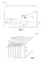
- FIG. 2Ashows a chip 200 in a stage of processing.
- the chip 200includes a semiconductor substrate 210 .
- the semiconductor substrate 210includes silicon.
- Other suitable semiconductor substrates 210include alternate semiconducting materials such as gallium arsenide, or composite substrate structures such as silicon-on-insulator structures.
- a number of devices 220are shown in schematic form, located on or within the substrate 210 .
- One common device 220includes a transistor, however the invention is not so limited.
- devices 220further include devices such as diodes, capacitors, etc.
- a number of through chip connection structures 230is also shown.
- the through chip connection structures 230are formed using a preferential etching process such as anodic etching to create a through chip channel with a high aspect ratio.
- the channelsare insulated by oxidation and later filled with a conductor such as a metal fill material to conduct signals through the chip 200 .
- the metal fill materialincludes aluminum metal.
- a bottom surface of the substrate 210is coupled to voltage source by a positive electrode. Further, a negative electrode is coupled to a voltage source and is placed in a bath of 6% aqueous solution of hydrofluoric acid (HF) on a surface of the substrate 210 .
- HFhydrofluoric acid
- the anodic etchetches high aspect ratio holes through substrate 210 at the location of etch pits.
- the voltage sourceis turned on and provides a voltage across positive and negative electrodes. Etching current flows from the surface to the positive electrode. This current forms the high aspect ratio holes through the substrate 210 .
- An anodic etching processis described in V. Lehmann, The Physics of Macropore Formation in Low Doped n - Type Silicon , J. Electrochem. Soc., Vol. 140, No. 10, pp. 2836-2843, October 1993, which is incorporated herein by reference.
- At least one through chip connection structure 230includes a coaxial conductor 232 .
- the connection structures 230 and/or coaxial conductors 232have an aspect ratio in the range of approximately 100 to 200.
- a semiconductor wafer used to form an integrated circuithas a thickness in the range of approximately 500 to 1000 microns.
- the through chip connection structures 230 and coaxial conductors 232can be fabricated with a width that is in the range from approximately 2.5 microns up to as much as approximately 10 microns.
- Even smaller through chip connectionscan be made in chips which are to be produced from wafers which are to be thinned after completion of the semiconductor processing. In this case, the small holes are processed, including the appropriate filling, to a depth which equals the thickness of the wafer after thinning. The wafers are thinned and connections are then made to the exposed through connections.
- Coaxial conductors 232include a center conductor 238 that is surrounded by insulator, e.g., oxide, 236 . Further, outer conductor 234 surrounds insulator 236 . Coaxial conductor 232 is shown in cross section in FIG. 2A . Outer conductor 234 comprises, for example, a metal layer that is deposited within a high aspect ratio via. Alternatively, outer conductor 234 may comprise a portion of the substrate 210 that has been doped with impurities to render it conductive.
- At least one through chip connection structure 230includes an optical waveguide.
- an optical waveguideincludes a reflective layer that is formed on inner surface of high aspect ratio holes.
- the reflective layerincludes a metallic mirror that is deposited with a self-limiting deposition process. This produces a reflective surface for an optical waveguide that is substantially uniform.
- the optical waveguidehas a center void that is essentially filled with air.
- a two-step, selective processis used in one embodiment to deposit tungsten as a portion of the reflective layer.
- Thisis a low-pressure chemical vapor deposition (LPCVD) process.
- LPCVDlow-pressure chemical vapor deposition
- atoms in the substrate 210e.g., silicon
- WF 6reaction gas
- the limiting thickness of this processis approximately 5 to 10 nanometers. This thickness may not be sufficient for a reflective layer.
- a second reduction processcan be used to complete the deposition of tungsten.
- This second reduction stepuses silane or polysilane and is thus referred to as a “silane reduction.”
- the silane reduction processalso uses WF 6 .
- a thin film of a material with a higher reflectivityis deposited on the tungsten material.
- a material with a higher reflectivityis deposited on the tungsten material.
- an aluminum filmcan be deposited at low temperature, e.g., in the range from 180° to 250° Celsius.
- through chip connection structures 230are used on a single chip, or within a multi-chip assembly. In one embodiment, one type of through chip connection structure 230 is selected and used throughout each single chip 200 , or a multi-chip assembly.
- FIG. 2Bshows a first insulator layer 240 attached to the chip 200 to isolate the number of devices 220 on a surface of the chip 200 .
- Suitable insulator layers 240include, but are not limited to oxides, or polymers such as polyimide.
- a number of vias or contacts 250are formed through the first insulator layer 240 to communicate with the number of devices 220 and the through chip connection structures 230 .
- a photolithographic processis used to pattern and remove selected portions of the first insulator layer 240 to form the vias or contacts 250 .
- FIG. 2Dshows a lateral connection structure 260 .
- the lateral connection structure 260is utilized for interconnecting selected devices 220 and/or connecting selected through chip connection structures 230 .
- the lateral connection structure 260includes a metalized layer such as a metal trace line.
- a large network of lateral connection structures 260such as metalized lines are used to connect devices on the chip 200 and form integrated circuits.
- at least one end 262 of a lateral connection structure 260is located adjacent to an edge 202 of the chip 200 .
- FIG. 2Eshows a second insulator layer 270 attached to the chip 200 to isolate the lateral connection structure or structures 260 .
- the second insulator layer 270includes a polymer layer.
- a suitable polymerincludes a polyimide. Some polyimides are able to withstand exposure to temperatures in a range from approximately 250-620° C. Endurance of the second insulator layer 270 at high temperatures is important because in some processes, the chip 200 is exposed to high processing temperatures before final manufacturing is complete. Suitable polyimides that posess a variety of physical properties include, but are not limited to, Type I, Type III, and Type V polyimides.
- polystyrene resinexamples include, for example, parylene, polynorbomenes and fluorinated polymers.
- Parylene-Nhas a melting point of 420° C., a tensile modulus of 2.4 GPa, and a yield strength of 42 MPa.
- One class of polynorbomeneincludes AvatrelTM polymer available from BF Goodrich, Cleveland, Ohio, USA.
- silaneis added to polynorbomenes to further lower the dielectric constant.
- Aerogelssuch as silica aerogel, may be utilized to provide porous insulating material of the various embodiments. Aerogels are generally a gel material that forms a porous matrix when liquid or solvent in the gel is replaced by air or another gaseous component. Aerogels generally experience only minimal volumetric change upon such curing.
- the polymeric materialis generally cured, or crosslinked, following formation.
- curingcan include an optional low temperature bake to drive off most of the solvents that may be present in the polymer prior to crosslinking.
- Other conventional polymerscan be cured by exposing them to visible or ultraviolet light.
- Still other conventional polymerscan be cured by adding curing (e.g., crosslinking) agents to the polymer.
- FIG. 2Fshows a number of connection structures 280 formed through the second insulator layer 270 to complete a signal pathway for the through chip connection structures 230 .
- the chip 200now contains at least two types of connection structures.
- One typeincludes the through chip connection structures 230 , which are designed to transmit signals substantially along direction 272 .
- Another typeincludes the lateral connection structures 260 , which are designed to transmit signals substantially along direction 262 .
- selected through chip connection structures 230are isolated from lateral connection structures 260 , and only transmit signals through the chip 200 . In one embodiment, selected through chip connection structures 230 are coupled to selected lateral connection structures 260 to communicate signals both through the chip 200 and laterally across the chip 200 .
- selected through chip connection structures 230are coupled to selected lateral connection structures 260 to communicate signals both through the chip 200 and laterally across the chip 200 .
- One of ordinary skill in the art, having the benefit of the present disclosurewill appreciate that a number of interconnection designs and combinations incorporating both through chip connection structures 230 and lateral connection structures 260 are possible depending on a given integrated circuit design and multi-chip assembly design.
- FIG. 2Gshows the chip 200 mounted to a carrier 204 .
- the carrier 204is used to facilitate thinning of the chip 200 .
- a beginning thickness 212 of the chip 200is indicated.
- the carrierincludes a sacrificial silicon wafer.
- Various methodsare possible for attaching the chip 200 to the surface of the carrier 204 .
- the chip 200is attached to the carrier using a water soluble epoxy, which facilitates removal of the chip 200 at a later stage of manufacturing.
- the chip 200is shown mounted with a backside facing upwards and exposed for a thinning operation.
- FIG. 2Hshows the chip 200 after a thinning process.
- the chip 200has been thinned to a thickness as indicated by 214 . Any of a number of acceptable thinning processes can be used.
- the chip 200is thinned using chemical mechanical polishing (CMP) techniques.
- CMPchemical mechanical polishing
- a deep implant of p+ carriersis implanted sufficient to a depth within the substrate 210 that is deeper than a maximum depth of the number of devices 220 .
- the through chip connection structures 230are formed to a depth that is deeper than the depth of the p+ deep implant.
- the thinning processcan then be set to stop at the depth from the backside of the chip 200 where the p+ layer is contacted. Using variations of this embodiment, the through chip connection structures 230 are exposed during the thinning process. Other embodiments are included that do not use the p+ deep implant and chip thinning technique.
- the second insulator layer 270includes cells of gaseous components. In one embodiment, an average cell size is less than 0.1 microns.
- a polymer second insulator layer 270is foamed to form cells of gaseous components.
- FIG. 2Hshows the second insulator layer 270 with a thickness 274 . In one embodiment, the thickness 274 is approximately 0.7 microns thick.
- FIG. 2Ishows a second thickness 276 of the second insulator layer 270 after a foaming process.
- the chip 200 in FIG. 2Jis shown without a carrier 204 . In one embodiment, the second thickness 276 is approximately 2.1 microns thick.
- the foaming processis performed after the chip is thinned, as described above, although the invention is not so limited.
- the cellsfunction to further reduce the dielectric constant.
- An increase in thickness of the second insulator layer 270also reduces unwanted capacitive effects.
- the cellsmay include air, or other gasses such as carbon dioxide.
- a supercritical fluidis utilized to convert at least a portion of the polymeric material, into a foamed polymeric material.
- Such use of supercritical fluidsfacilitates formation of sub-micron cells in the foamed polymeric material.
- a gasis determined to be in a supercritical state (and is referred to as a supercritical fluid) when it is subjected to a combination of pressure and temperature above its critical point, such that its density approaches that of a liquid (i.e., the liquid and gas states are indistinguishable).
- a supercritical fluidis determined to be in a supercritical state (and is referred to as a supercritical fluid) when it is subjected to a combination of pressure and temperature above its critical point, such that its density approaches that of a liquid (i.e., the liquid and gas states are indistinguishable).
- a wide variety of compounds and elementscan be converted to the supercritical state in order to be used to form the second insulator layer 270 .
- Suitable supercritical fluidsinclude, but are not limited to: ammonia (NH 3 ), an amine (NR 3 ), an alcohol (ROH), water (H 2 O), carbon dioxide (CO 2 ), nitrous oxide (N 2 O), a noble gas (e.g., He, Ne, Ar), a hydrogen halide (e.g., hydrofluoric acid (HF), hydrochloric acid (HCl), hydrobromic acid (HBr)), boron trichloride (BCl 3 ), chlorine (Cl 2 ), fluorine (F 2 ), oxygen (O 2 ) nitrogen (N 2 ), a hydrocarbon (e.g., dimethyl carbonate (CO(OCH 3 ) 2 ), methane (CH 4 ), ethane (C 2 H 6 ), propane (C 3 H 8 ), ethylene (C 2 H 4 ), etc.), a fluorocarbon (e.g., CF 4 , C 2 F 4 , CH 3 F, etc.), hexafluoro
- a fluid with a low critical pressurepreferably below about 100 atmospheres, and a low critical temperature of at or near room temperature.
- the fluidsbe nontoxic and nonflammable.
- the fluidsshould not degrade the properties of the polymeric material.
- supercritical fluid CO 2is utilized, due to the relatively inert nature of CO 2 with respect to most polymeric materials as well as other materials utilized in integrated circuit fabrication.
- a selected polymer in one embodiment of a second insulator layer 270is exposed to the supercritical fluid for a sufficient time period to foam at least a portion of the polymeric material.
- the chip 200is placed in a processing chamber, and the temperature and pressure of the processing chamber are elevated above the temperature and pressure needed for creating and maintaining the particular supercritical fluid.
- the flow of supercritical fluidis stopped and the processing chamber is depressurized. Upon depressurization, the foaming of the polymeric material occurs as the supercritical state of the fluid is no longer maintained, and cells are formed in the polymeric material.
- foamsmay also be formed by use of block co-polymers.
- polymer materialssuch as embodiments of the second insulator layer 270 , include hydrophilic polymers.
- hydrophilic polymersare advantageous because moisture is attracted away from metal or semiconductor devices in the chip 200 where water could cause corrosion damage.
- a hydrophilic treatmentis added to whatever polymer or insulator layer is selected.
- the hydrophilic treatmentincludes introduction of methane radicals to a surface of the insulator layer.
- the methane radicalsare created using a high frequency electric field.
- the insulator layercan be selected based on other material properties such as dielectric constant, and the additional desirable property of a hydrophilic nature can be added to the chosen material.
- FIG. 2Jshows the chip 200 from another angle to further illustrate possible locations of structures in the chip 200 as described above.
- the number of devices 220are shown, with the lateral connection structure 260 coupling to the illustrated devices 220 .
- the lateral connection structure 260includes an end 262 that is adjacent to a chip edge as described above.
- the number of through chip connection structures 230are shown in various locations on the chip 200 .
- selected through chip connection structures 230such as individual structure 231 are coupled to other circuitry such as the lateral connection structure 260 .
- a selected through chip connection structure 230is shown as a coaxial structure 232 .
- coaxial structures 232are one possible embodiment of through chip connection structures 230 .
- selected chip connection structuresincluding through chip connection structures 230 and lateral connection structure 260 are coupled to terminal metals to facilitate later connection to other chips.
- terminal metalsinclude ZrNiCuAu pads and solder applied to aluminum contact metal.
- FIG. 3illustrates one example of a multi-chip assembly 300 using embodiments of chips as described in embodiments above.
- a number of chips 310are shown coupled together to form an assembly.
- the assembly 300includes a cube like assembly, although the invention is not so limited.
- Other geometries of multi-chip assembliesare possible, such as rectangular assemblies, or other complex geometries that utilize through chip connection structures and lateral connection structures are within the scope of the invention.
- a number of chip edge connections 320are illustrated.
- the chip edge connections 320are formed by removing material from the edges of chips 310 to expose lateral connection structures as described in embodiments above. In one embodiment, removing material includes etching back the edges of the chips 310 .
- a number of chip edge interconnects 330are also shown coupling selected chip edge connections 320 . In one embodiment, the chip edge interconnects 330 include metal trace lines.
- the number of chips 310include both memory chips such as DRAM, SRAM, or flash chips. In one embodiment, the number of chips 310 also includes at least one logic chip. As discussed above, logic chips include processor chips, or other specialized logic chips such as analog to digital converter chips. In one embodiment, a processor chip is included as a logic chip, and is located on an external surface of the multi-chip assembly 300 . Location on an external surface is advantageous because cooling is enhanced on external surfaces of the multi-chip assembly 300 . Logic chips such as processor chips tend to generate large amounts of heat compared to memory chips, therefore location of logic chips on external surfaces is desired. In some embodiments, multiple logic or processor chips are included, and external surfaces may not be available for all logic chips. In embodiments such as these, logic chips may be located internal to the multi-chip assembly 300 .
- the multi-chip assembly 300includes chips with both lateral connection structures and through chip connection structures as described in embodiments above.
- the use of both lateral connection structures and through chip connection structuresis advantageous because more pathways are available for the chips 310 in the multi-chip assembly 300 to communicate with each other. If only edge connections were used, the number of connections would be limited to the space on the edge of the chips.
- a multi-chip assembly 300is able to also utilize through chip connection structures to increase the number of connections between chips.
- connection pathway directly through the middle of a chip using a through chip connectionis significantly shorter than connecting out to an edge of one chip, then back into another chip from that chip edge. Shorter connection pathways lead to increased speed and performance of multi-chip assemblies 300 .
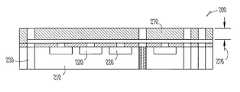
- FIG. 4shows an embodiment of a multi-chip assembly 400 .
- a number of chips 410are shown coupled together to form the assembly 400 .
- the multi-chip assembly 400is shown attached to a surface 402 such as a motherboard.
- a number of chip edge connections 420are illustrated.
- the chip edge connections 420are formed by removing material from the edges of chips 410 to expose lateral connection structures as described in embodiments above. In one embodiment, removing material includes etching back the edges of the chips 410 .
- a number of chip edge interconnects 430are also shown coupling selected chip edge connections 420 . In one embodiment, the chip edge interconnects 430 include metal trace lines.
- At least one logic chipsuch as a processor, is included in the number of chips 410 .
- a logic chipis shown coupled to the top of the multi-chip assembly 400 .
- a second number of chip edge interconnects 440is shown coupling to this logic chip.
- the second number of chip edge interconnects 440illustrate one possible connection method to connect chips that are orthogonal to each other. Although the figure illustrates orthogonal chips, other angles apart from 90 degrees are possible between chips of the multi-chip assembly 400 .
- corner connection structure 450includes a first conducting pillar 452 , a second conducting pillar 454 and a solder ball 456 .
- Other embodiments of corner connection structuresare also included within the scope of the invention. Acceptable devices and methods are described in commonly assigned U.S. Pat. No. 6,552,424 which is incorporated herein by reference in its entirety.
- a multi-chip assemblyuses both lateral connection structures and through chip connection structures.
- One advantage of this designincludes an increased number of possible connections.
- Another advantage of this designincludes shorter distances for interconnection pathways, which improves device performance and speed. Numerous other advantages are provided by embodiments described above, including but not limited to: decreased capacitive coupling from improved isolation structures and materials; decreased corrosion probability due to hydrophilic materials; improved cooling due to locations of logic chips; reduced assembly size due to thinning of chips; etc.
Landscapes
- Engineering & Computer Science (AREA)
- Microelectronics & Electronic Packaging (AREA)
- Power Engineering (AREA)
- Physics & Mathematics (AREA)
- Condensed Matter Physics & Semiconductors (AREA)
- General Physics & Mathematics (AREA)
- Computer Hardware Design (AREA)
- Semiconductor Integrated Circuits (AREA)
- Internal Circuitry In Semiconductor Integrated Circuit Devices (AREA)
- Semiconductor Memories (AREA)
Abstract
Description
Claims (18)
Priority Applications (2)
| Application Number | Priority Date | Filing Date | Title |
|---|---|---|---|
| US11/458,859US8592964B2 (en) | 2003-09-03 | 2006-07-20 | Apparatus and method for high density multi-chip structures |
| US14/087,696US9209127B2 (en) | 2003-09-03 | 2013-11-22 | Apparatus and method for high density multi-chip structures |
Applications Claiming Priority (3)
| Application Number | Priority Date | Filing Date | Title |
|---|---|---|---|
| US10/654,038US20050046034A1 (en) | 2003-09-03 | 2003-09-03 | Apparatus and method for high density multi-chip structures |
| US11/218,092US7560305B2 (en) | 2003-09-03 | 2005-08-31 | Apparatus and method for high density multi-chip structures |
| US11/458,859US8592964B2 (en) | 2003-09-03 | 2006-07-20 | Apparatus and method for high density multi-chip structures |
Related Parent Applications (2)
| Application Number | Title | Priority Date | Filing Date |
|---|---|---|---|
| US10/654,038DivisionUS20050046034A1 (en) | 2003-09-03 | 2003-09-03 | Apparatus and method for high density multi-chip structures |
| US11/218,092DivisionUS7560305B2 (en) | 2003-09-03 | 2005-08-31 | Apparatus and method for high density multi-chip structures |
Related Child Applications (1)
| Application Number | Title | Priority Date | Filing Date |
|---|---|---|---|
| US14/087,696ContinuationUS9209127B2 (en) | 2003-09-03 | 2013-11-22 | Apparatus and method for high density multi-chip structures |
Publications (2)
| Publication Number | Publication Date |
|---|---|
| US20060289990A1 US20060289990A1 (en) | 2006-12-28 |
| US8592964B2true US8592964B2 (en) | 2013-11-26 |
Family
ID=34218000
Family Applications (4)
| Application Number | Title | Priority Date | Filing Date |
|---|---|---|---|
| US10/654,038AbandonedUS20050046034A1 (en) | 2003-09-03 | 2003-09-03 | Apparatus and method for high density multi-chip structures |
| US11/218,092Expired - Fee RelatedUS7560305B2 (en) | 2003-09-03 | 2005-08-31 | Apparatus and method for high density multi-chip structures |
| US11/458,859Expired - LifetimeUS8592964B2 (en) | 2003-09-03 | 2006-07-20 | Apparatus and method for high density multi-chip structures |
| US14/087,696Expired - LifetimeUS9209127B2 (en) | 2003-09-03 | 2013-11-22 | Apparatus and method for high density multi-chip structures |
Family Applications Before (2)
| Application Number | Title | Priority Date | Filing Date |
|---|---|---|---|
| US10/654,038AbandonedUS20050046034A1 (en) | 2003-09-03 | 2003-09-03 | Apparatus and method for high density multi-chip structures |
| US11/218,092Expired - Fee RelatedUS7560305B2 (en) | 2003-09-03 | 2005-08-31 | Apparatus and method for high density multi-chip structures |
Family Applications After (1)
| Application Number | Title | Priority Date | Filing Date |
|---|---|---|---|
| US14/087,696Expired - LifetimeUS9209127B2 (en) | 2003-09-03 | 2013-11-22 | Apparatus and method for high density multi-chip structures |
Country Status (1)
| Country | Link |
|---|---|
| US (4) | US20050046034A1 (en) |
Cited By (1)
| Publication number | Priority date | Publication date | Assignee | Title |
|---|---|---|---|---|
| US9209127B2 (en) | 2003-09-03 | 2015-12-08 | Micron Technology | Apparatus and method for high density multi-chip structures |
Families Citing this family (25)
| Publication number | Priority date | Publication date | Assignee | Title |
|---|---|---|---|---|
| US7831151B2 (en) | 2001-06-29 | 2010-11-09 | John Trezza | Redundant optical device array |
| US7786592B2 (en) | 2005-06-14 | 2010-08-31 | John Trezza | Chip capacitive coupling |
| US7781886B2 (en) | 2005-06-14 | 2010-08-24 | John Trezza | Electronic chip contact structure |
| US20060281303A1 (en)* | 2005-06-14 | 2006-12-14 | John Trezza | Tack & fuse chip bonding |
| US7687400B2 (en)* | 2005-06-14 | 2010-03-30 | John Trezza | Side stacking apparatus and method |
| US7560813B2 (en) | 2005-06-14 | 2009-07-14 | John Trezza | Chip-based thermo-stack |
| US7851348B2 (en)* | 2005-06-14 | 2010-12-14 | Abhay Misra | Routingless chip architecture |
| US8456015B2 (en)* | 2005-06-14 | 2013-06-04 | Cufer Asset Ltd. L.L.C. | Triaxial through-chip connection |
| US7534722B2 (en)* | 2005-06-14 | 2009-05-19 | John Trezza | Back-to-front via process |
| US7838997B2 (en)* | 2005-06-14 | 2010-11-23 | John Trezza | Remote chip attachment |
| US7989958B2 (en)* | 2005-06-14 | 2011-08-02 | Cufer Assett Ltd. L.L.C. | Patterned contact |
| US7767493B2 (en)* | 2005-06-14 | 2010-08-03 | John Trezza | Post & penetration interconnection |
| US7521806B2 (en)* | 2005-06-14 | 2009-04-21 | John Trezza | Chip spanning connection |
| US7633167B2 (en)* | 2005-09-29 | 2009-12-15 | Nec Electronics Corporation | Semiconductor device and method for manufacturing same |
| US7687397B2 (en) | 2006-06-06 | 2010-03-30 | John Trezza | Front-end processed wafer having through-chip connections |
| US20070281460A1 (en)* | 2006-06-06 | 2007-12-06 | Cubic Wafer, Inc. | Front-end processed wafer having through-chip connections |
| JP5269799B2 (en)* | 2006-10-17 | 2013-08-21 | キューファー アセット リミテッド. エル.エル.シー. | Wafer via formation |
| US7670874B2 (en)* | 2007-02-16 | 2010-03-02 | John Trezza | Plated pillar package formation |
| US7850060B2 (en)* | 2007-04-05 | 2010-12-14 | John Trezza | Heat cycle-able connection |
| US7748116B2 (en)* | 2007-04-05 | 2010-07-06 | John Trezza | Mobile binding in an electronic connection |
| US7960210B2 (en)* | 2007-04-23 | 2011-06-14 | Cufer Asset Ltd. L.L.C. | Ultra-thin chip packaging |
| US20080261392A1 (en)* | 2007-04-23 | 2008-10-23 | John Trezza | Conductive via formation |
| KR101374338B1 (en)* | 2007-11-14 | 2014-03-14 | 삼성전자주식회사 | semicondoctor device having through-via and method of forming the same |
| TWI457645B (en)* | 2010-07-22 | 2014-10-21 | Innolux Corp | Touch display device |
| US8587088B2 (en)* | 2011-02-17 | 2013-11-19 | Apple Inc. | Side-mounted controller and methods for making the same |
Citations (35)
| Publication number | Priority date | Publication date | Assignee | Title |
|---|---|---|---|---|
| US4525921A (en) | 1981-07-13 | 1985-07-02 | Irvine Sensors Corporation | High-density electronic processing package-structure and fabrication |
| US4617160A (en) | 1984-11-23 | 1986-10-14 | Irvine Sensors Corporation | Method for fabricating modules comprising uniformly stacked, aligned circuit-carrying layers |
| US4706166A (en) | 1986-04-25 | 1987-11-10 | Irvine Sensors Corporation | High-density electronic modules--process and product |
| US4868712A (en)* | 1987-02-04 | 1989-09-19 | Woodman John K | Three dimensional integrated circuit package |
| US5158986A (en) | 1991-04-05 | 1992-10-27 | Massachusetts Institute Of Technology | Microcellular thermoplastic foamed with supercritical fluid |
| US5202754A (en) | 1991-09-13 | 1993-04-13 | International Business Machines Corporation | Three-dimensional multichip packages and methods of fabrication |
| US5270261A (en) | 1991-09-13 | 1993-12-14 | International Business Machines Corporation | Three dimensional multichip package methods of fabrication |
| US5347428A (en)* | 1992-12-03 | 1994-09-13 | Irvine Sensors Corporation | Module comprising IC memory stack dedicated to and structurally combined with an IC microprocessor chip |
| US5424920A (en)* | 1992-05-15 | 1995-06-13 | Irvine Sensors Corporation | Non-conductive end layer for integrated stack of IC chips |
| US5478781A (en) | 1993-06-21 | 1995-12-26 | International Business Machines Corporation | Polyimide-insulated cube package of stacked semiconductor device chips |
| US5506753A (en) | 1994-09-26 | 1996-04-09 | International Business Machines Corporation | Method and apparatus for a stress relieved electronic module |
| US5581498A (en) | 1993-08-13 | 1996-12-03 | Irvine Sensors Corporation | Stack of IC chips in lieu of single IC chip |
| US5583958A (en)* | 1994-09-28 | 1996-12-10 | The Furukawa Electric Co., Ltd. | Composite optical device |
| US5620742A (en) | 1992-10-09 | 1997-04-15 | Mcneil-Ppc, Inc. | Method for making absorbent articles having printed polymer coatings |
| US5658451A (en)* | 1995-02-01 | 1997-08-19 | Avl Medical Instruments Ag | Method for calibration of a pH measuring element |
| US5807791A (en) | 1995-02-22 | 1998-09-15 | International Business Machines Corporation | Methods for fabricating multichip semiconductor structures with consolidated circuitry and programmable ESD protection for input/output nodes |
| US5903045A (en) | 1996-04-30 | 1999-05-11 | International Business Machines Corporation | Self-aligned connector for stacked chip module |
| US6077792A (en) | 1997-07-14 | 2000-06-20 | Micron Technology, Inc. | Method of forming foamed polymeric material for an integrated circuit |
| US6090636A (en)* | 1998-02-26 | 2000-07-18 | Micron Technology, Inc. | Integrated circuits using optical waveguide interconnects formed through a semiconductor wafer and methods for forming same |
| US6122187A (en)* | 1998-11-23 | 2000-09-19 | Micron Technology, Inc. | Stacked integrated circuits |
| US6136689A (en) | 1998-08-14 | 2000-10-24 | Micron Technology, Inc. | Method of forming a micro solder ball for use in C4 bonding process |
| US6143616A (en) | 1997-08-22 | 2000-11-07 | Micron Technology, Inc. | Methods of forming coaxial integrated circuitry interconnect lines |
| US6150188A (en) | 1998-02-26 | 2000-11-21 | Micron Technology Inc. | Integrated circuits using optical fiber interconnects formed through a semiconductor wafer and methods for forming same |
| US6198168B1 (en) | 1998-01-20 | 2001-03-06 | Micron Technologies, Inc. | Integrated circuits using high aspect ratio vias through a semiconductor wafer and method for forming same |
| US6383924B1 (en) | 2000-12-13 | 2002-05-07 | Micron Technology, Inc. | Method of forming buried conductor patterns by surface transformation of empty spaces in solid state materials |
| US20020117742A1 (en)* | 1999-07-30 | 2002-08-29 | Hitachi, Ltd. | Semiconductor device |
| US6521512B2 (en) | 2000-10-04 | 2003-02-18 | Infineon Technologies Ag | Method for fabricating a thin, free-standing semiconductor device layer and for making a three-dimensionally integrated circuit |
| US6535320B1 (en)* | 2000-09-15 | 2003-03-18 | The United States Of America As Represented By The Secretary Of The Navy | Traveling wave, linearized reflection modulator |
| US6566232B1 (en)* | 1999-10-22 | 2003-05-20 | Seiko Epson Corporation | Method of fabricating semiconductor device |
| US6633081B2 (en) | 2001-05-30 | 2003-10-14 | Matsushita Electric Industrial Co., Ltd. | Semiconductor device on a packaging substrate |
| US20030230792A1 (en) | 2002-06-14 | 2003-12-18 | Siliconware Precision Industries Co., Ltd. | Flip-chip semiconductor package with lead frame as chip carrier and fabrication method thereof |
| US6781241B2 (en) | 2002-04-19 | 2004-08-24 | Fujitsu Limited | Semiconductor device and manufacturing method thereof |
| US20040251557A1 (en)* | 2003-06-16 | 2004-12-16 | Sandisk Corporation | Integrated circuit package having stacked integrated circuits and method therefor |
| US20050046034A1 (en) | 2003-09-03 | 2005-03-03 | Micron Technology, Inc. | Apparatus and method for high density multi-chip structures |
| US6879757B1 (en)* | 2001-12-11 | 2005-04-12 | Phosistor Technologies, Inc. | Connection between a waveguide array and a fiber array |
Family Cites Families (3)
| Publication number | Priority date | Publication date | Assignee | Title |
|---|---|---|---|---|
| US5158966A (en)* | 1991-02-22 | 1992-10-27 | The University Of Colorado Foundation, Inc. | Method of treating type i diabetes |
| US6469375B2 (en)* | 2001-02-28 | 2002-10-22 | William F. Beausoleil | High bandwidth 3D memory packaging technique |
| US6433413B1 (en)* | 2001-08-17 | 2002-08-13 | Micron Technology, Inc. | Three-dimensional multichip module |
- 2003
- 2003-09-03USUS10/654,038patent/US20050046034A1/ennot_activeAbandoned
- 2005
- 2005-08-31USUS11/218,092patent/US7560305B2/ennot_activeExpired - Fee Related
- 2006
- 2006-07-20USUS11/458,859patent/US8592964B2/ennot_activeExpired - Lifetime
- 2013
- 2013-11-22USUS14/087,696patent/US9209127B2/ennot_activeExpired - Lifetime
Patent Citations (40)
| Publication number | Priority date | Publication date | Assignee | Title |
|---|---|---|---|---|
| US4525921A (en) | 1981-07-13 | 1985-07-02 | Irvine Sensors Corporation | High-density electronic processing package-structure and fabrication |
| US4617160A (en) | 1984-11-23 | 1986-10-14 | Irvine Sensors Corporation | Method for fabricating modules comprising uniformly stacked, aligned circuit-carrying layers |
| US4706166A (en) | 1986-04-25 | 1987-11-10 | Irvine Sensors Corporation | High-density electronic modules--process and product |
| US4868712A (en)* | 1987-02-04 | 1989-09-19 | Woodman John K | Three dimensional integrated circuit package |
| US5158986A (en) | 1991-04-05 | 1992-10-27 | Massachusetts Institute Of Technology | Microcellular thermoplastic foamed with supercritical fluid |
| US5334356A (en) | 1991-04-05 | 1994-08-02 | Massachusetts Institute Of Technology | Supermicrocellular foamed materials |
| US5202754A (en) | 1991-09-13 | 1993-04-13 | International Business Machines Corporation | Three-dimensional multichip packages and methods of fabrication |
| US5270261A (en) | 1991-09-13 | 1993-12-14 | International Business Machines Corporation | Three dimensional multichip package methods of fabrication |
| US5424920A (en)* | 1992-05-15 | 1995-06-13 | Irvine Sensors Corporation | Non-conductive end layer for integrated stack of IC chips |
| US5620742A (en) | 1992-10-09 | 1997-04-15 | Mcneil-Ppc, Inc. | Method for making absorbent articles having printed polymer coatings |
| US5347428A (en)* | 1992-12-03 | 1994-09-13 | Irvine Sensors Corporation | Module comprising IC memory stack dedicated to and structurally combined with an IC microprocessor chip |
| US5478781A (en) | 1993-06-21 | 1995-12-26 | International Business Machines Corporation | Polyimide-insulated cube package of stacked semiconductor device chips |
| US5581498A (en) | 1993-08-13 | 1996-12-03 | Irvine Sensors Corporation | Stack of IC chips in lieu of single IC chip |
| US5506753A (en) | 1994-09-26 | 1996-04-09 | International Business Machines Corporation | Method and apparatus for a stress relieved electronic module |
| US5583958A (en)* | 1994-09-28 | 1996-12-10 | The Furukawa Electric Co., Ltd. | Composite optical device |
| US5658451A (en)* | 1995-02-01 | 1997-08-19 | Avl Medical Instruments Ag | Method for calibration of a pH measuring element |
| US5807791A (en) | 1995-02-22 | 1998-09-15 | International Business Machines Corporation | Methods for fabricating multichip semiconductor structures with consolidated circuitry and programmable ESD protection for input/output nodes |
| US5903045A (en) | 1996-04-30 | 1999-05-11 | International Business Machines Corporation | Self-aligned connector for stacked chip module |
| US6077792A (en) | 1997-07-14 | 2000-06-20 | Micron Technology, Inc. | Method of forming foamed polymeric material for an integrated circuit |
| US6143616A (en) | 1997-08-22 | 2000-11-07 | Micron Technology, Inc. | Methods of forming coaxial integrated circuitry interconnect lines |
| US6313531B1 (en) | 1997-08-22 | 2001-11-06 | Micron Technology, Inc. | Coaxial integrated circuitry interconnect lines, and integrated circuitry |
| US6198168B1 (en) | 1998-01-20 | 2001-03-06 | Micron Technologies, Inc. | Integrated circuits using high aspect ratio vias through a semiconductor wafer and method for forming same |
| US6090636A (en)* | 1998-02-26 | 2000-07-18 | Micron Technology, Inc. | Integrated circuits using optical waveguide interconnects formed through a semiconductor wafer and methods for forming same |
| US6526191B1 (en) | 1998-02-26 | 2003-02-25 | Micron Technology, Inc. | Integrated circuits using optical fiber interconnects formed through a semiconductor wafer and methods for forming same |
| US6150188A (en) | 1998-02-26 | 2000-11-21 | Micron Technology Inc. | Integrated circuits using optical fiber interconnects formed through a semiconductor wafer and methods for forming same |
| US6136689A (en) | 1998-08-14 | 2000-10-24 | Micron Technology, Inc. | Method of forming a micro solder ball for use in C4 bonding process |
| US6122187A (en)* | 1998-11-23 | 2000-09-19 | Micron Technology, Inc. | Stacked integrated circuits |
| US20020117742A1 (en)* | 1999-07-30 | 2002-08-29 | Hitachi, Ltd. | Semiconductor device |
| US6566232B1 (en)* | 1999-10-22 | 2003-05-20 | Seiko Epson Corporation | Method of fabricating semiconductor device |
| US6535320B1 (en)* | 2000-09-15 | 2003-03-18 | The United States Of America As Represented By The Secretary Of The Navy | Traveling wave, linearized reflection modulator |
| US6521512B2 (en) | 2000-10-04 | 2003-02-18 | Infineon Technologies Ag | Method for fabricating a thin, free-standing semiconductor device layer and for making a three-dimensionally integrated circuit |
| US6383924B1 (en) | 2000-12-13 | 2002-05-07 | Micron Technology, Inc. | Method of forming buried conductor patterns by surface transformation of empty spaces in solid state materials |
| US6633081B2 (en) | 2001-05-30 | 2003-10-14 | Matsushita Electric Industrial Co., Ltd. | Semiconductor device on a packaging substrate |
| US6879757B1 (en)* | 2001-12-11 | 2005-04-12 | Phosistor Technologies, Inc. | Connection between a waveguide array and a fiber array |
| US6781241B2 (en) | 2002-04-19 | 2004-08-24 | Fujitsu Limited | Semiconductor device and manufacturing method thereof |
| US20030230792A1 (en) | 2002-06-14 | 2003-12-18 | Siliconware Precision Industries Co., Ltd. | Flip-chip semiconductor package with lead frame as chip carrier and fabrication method thereof |
| US20040251557A1 (en)* | 2003-06-16 | 2004-12-16 | Sandisk Corporation | Integrated circuit package having stacked integrated circuits and method therefor |
| US20050046034A1 (en) | 2003-09-03 | 2005-03-03 | Micron Technology, Inc. | Apparatus and method for high density multi-chip structures |
| US20060063302A1 (en) | 2003-09-03 | 2006-03-23 | Micron Technology, Inc. | Apparatus and method for high density multi-chip structures |
| US7560305B2 (en) | 2003-09-03 | 2009-07-14 | Micron Technology, Inc. | Apparatus and method for high density multi-chip structures |
Non-Patent Citations (4)
| Title |
|---|
| Chiniwalla, P., "Structure-Property Relations for Polynorbornenes", Proceedings from the Eighth Meeting of the Dupont Symposium on Polymides in Microelectronics, (1998),615-642. |
| Jayaraj, K., "Low Dielectric COnstant Microcellular Foams", Proceedings from the Seventh Meeting of the DuPont Symposium on on Polymides in Microelectrics, (Sep. 1996),474-501. |
| Miller, R. D., "Low Dielectric Constant Polyimides and Polyimide Nanofoams", Seventh Meeting of the DuPont Symposium on Polvmides in Microelectronics, (Sep. 1996),443-473. |
| Ting, Chiu H., "Low K Material/Process Development", 1996 VLSI Multilevel Interconnection State-of-the-Art Seminar, (Jun. 1996),171-212. |
Cited By (1)
| Publication number | Priority date | Publication date | Assignee | Title |
|---|---|---|---|---|
| US9209127B2 (en) | 2003-09-03 | 2015-12-08 | Micron Technology | Apparatus and method for high density multi-chip structures |
Also Published As
| Publication number | Publication date |
|---|---|
| US7560305B2 (en) | 2009-07-14 |
| US20060289990A1 (en) | 2006-12-28 |
| US20060063302A1 (en) | 2006-03-23 |
| US20140077393A1 (en) | 2014-03-20 |
| US9209127B2 (en) | 2015-12-08 |
| US20050046034A1 (en) | 2005-03-03 |
Similar Documents
| Publication | Publication Date | Title |
|---|---|---|
| US8592964B2 (en) | Apparatus and method for high density multi-chip structures | |
| US6495445B2 (en) | Semi-sacrificial diamond for air dielectric formation | |
| US6737723B2 (en) | Low dielectric constant shallow trench isolation | |
| US8847405B2 (en) | Integrated circuits including air gaps around interconnect structures, and fabrication methods thereof | |
| US6255712B1 (en) | Semi-sacrificial diamond for air dielectric formation | |
| US6953983B2 (en) | Low dielectric constant STI with SOI devices | |
| US20090179331A1 (en) | Integrated circuit insulators and related methods | |
| US20200227272A1 (en) | Interconnect Structure with Porous Low K Film | |
| US7276788B1 (en) | Hydrophobic foamed insulators for high density circuits | |
| CN100372113C (en) | Integrated circuit structure with air space and manufacturing method thereof | |
| US7199043B2 (en) | Method of forming copper wiring in semiconductor device | |
| US20220084942A1 (en) | Metallization stacks with self-aligned staggered metal lines | |
| US7338897B2 (en) | Method of fabricating a semiconductor device having metal wiring | |
| US7015589B2 (en) | Semiconductor device having low-k dielectric film in pad region | |
| CN109427649B (en) | Semiconductor structure and forming method thereof | |
| KR100546940B1 (en) | Copper wiring formation method of semiconductor device | |
| KR20050006468A (en) | Method of forming copper wiring in semiconductor device | |
| KR20030089921A (en) | method for forming an insulation layer and a semiconductor device using the same | |
| KR20050063038A (en) | Method for forming a metal wire layer having damascene structure in a semiconductor device |
Legal Events
| Date | Code | Title | Description |
|---|---|---|---|
| FEPP | Fee payment procedure | Free format text:PAYOR NUMBER ASSIGNED (ORIGINAL EVENT CODE: ASPN); ENTITY STATUS OF PATENT OWNER: LARGE ENTITY | |
| STCF | Information on status: patent grant | Free format text:PATENTED CASE | |
| AS | Assignment | Owner name:MICRON TECHNOLOGY, INC., IDAHO Free format text:ASSIGNMENT OF ASSIGNORS INTEREST;ASSIGNOR:FARRAR, PAUL A.;REEL/FRAME:032363/0764 Effective date:20030822 | |
| AS | Assignment | Owner name:U.S. BANK NATIONAL ASSOCIATION, AS COLLATERAL AGENT, CALIFORNIA Free format text:SECURITY INTEREST;ASSIGNOR:MICRON TECHNOLOGY, INC.;REEL/FRAME:038669/0001 Effective date:20160426 Owner name:U.S. BANK NATIONAL ASSOCIATION, AS COLLATERAL AGEN Free format text:SECURITY INTEREST;ASSIGNOR:MICRON TECHNOLOGY, INC.;REEL/FRAME:038669/0001 Effective date:20160426 | |
| AS | Assignment | Owner name:MORGAN STANLEY SENIOR FUNDING, INC., AS COLLATERAL AGENT, MARYLAND Free format text:PATENT SECURITY AGREEMENT;ASSIGNOR:MICRON TECHNOLOGY, INC.;REEL/FRAME:038954/0001 Effective date:20160426 Owner name:MORGAN STANLEY SENIOR FUNDING, INC., AS COLLATERAL Free format text:PATENT SECURITY AGREEMENT;ASSIGNOR:MICRON TECHNOLOGY, INC.;REEL/FRAME:038954/0001 Effective date:20160426 | |
| FPAY | Fee payment | Year of fee payment:4 | |
| AS | Assignment | Owner name:U.S. BANK NATIONAL ASSOCIATION, AS COLLATERAL AGENT, CALIFORNIA Free format text:CORRECTIVE ASSIGNMENT TO CORRECT THE REPLACE ERRONEOUSLY FILED PATENT #7358718 WITH THE CORRECT PATENT #7358178 PREVIOUSLY RECORDED ON REEL 038669 FRAME 0001. ASSIGNOR(S) HEREBY CONFIRMS THE SECURITY INTEREST;ASSIGNOR:MICRON TECHNOLOGY, INC.;REEL/FRAME:043079/0001 Effective date:20160426 Owner name:U.S. BANK NATIONAL ASSOCIATION, AS COLLATERAL AGEN Free format text:CORRECTIVE ASSIGNMENT TO CORRECT THE REPLACE ERRONEOUSLY FILED PATENT #7358718 WITH THE CORRECT PATENT #7358178 PREVIOUSLY RECORDED ON REEL 038669 FRAME 0001. ASSIGNOR(S) HEREBY CONFIRMS THE SECURITY INTEREST;ASSIGNOR:MICRON TECHNOLOGY, INC.;REEL/FRAME:043079/0001 Effective date:20160426 | |
| AS | Assignment | Owner name:JPMORGAN CHASE BANK, N.A., AS COLLATERAL AGENT, ILLINOIS Free format text:SECURITY INTEREST;ASSIGNORS:MICRON TECHNOLOGY, INC.;MICRON SEMICONDUCTOR PRODUCTS, INC.;REEL/FRAME:047540/0001 Effective date:20180703 Owner name:JPMORGAN CHASE BANK, N.A., AS COLLATERAL AGENT, IL Free format text:SECURITY INTEREST;ASSIGNORS:MICRON TECHNOLOGY, INC.;MICRON SEMICONDUCTOR PRODUCTS, INC.;REEL/FRAME:047540/0001 Effective date:20180703 | |
| AS | Assignment | Owner name:MICRON TECHNOLOGY, INC., IDAHO Free format text:RELEASE BY SECURED PARTY;ASSIGNOR:U.S. BANK NATIONAL ASSOCIATION, AS COLLATERAL AGENT;REEL/FRAME:047243/0001 Effective date:20180629 | |
| AS | Assignment | Owner name:MICRON TECHNOLOGY, INC., IDAHO Free format text:RELEASE BY SECURED PARTY;ASSIGNOR:MORGAN STANLEY SENIOR FUNDING, INC., AS COLLATERAL AGENT;REEL/FRAME:050937/0001 Effective date:20190731 | |
| AS | Assignment | Owner name:MICRON SEMICONDUCTOR PRODUCTS, INC., IDAHO Free format text:RELEASE BY SECURED PARTY;ASSIGNOR:JPMORGAN CHASE BANK, N.A., AS COLLATERAL AGENT;REEL/FRAME:051028/0001 Effective date:20190731 Owner name:MICRON TECHNOLOGY, INC., IDAHO Free format text:RELEASE BY SECURED PARTY;ASSIGNOR:JPMORGAN CHASE BANK, N.A., AS COLLATERAL AGENT;REEL/FRAME:051028/0001 Effective date:20190731 | |
| MAFP | Maintenance fee payment | Free format text:PAYMENT OF MAINTENANCE FEE, 8TH YEAR, LARGE ENTITY (ORIGINAL EVENT CODE: M1552); ENTITY STATUS OF PATENT OWNER: LARGE ENTITY Year of fee payment:8 | |
| FEPP | Fee payment procedure | Free format text:MAINTENANCE FEE REMINDER MAILED (ORIGINAL EVENT CODE: REM.); ENTITY STATUS OF PATENT OWNER: LARGE ENTITY |