US8590010B2 - Retention based intrinsic fingerprint identification featuring a fuzzy algorithm and a dynamic key - Google Patents
Retention based intrinsic fingerprint identification featuring a fuzzy algorithm and a dynamic keyDownload PDFInfo
- Publication number
- US8590010B2 US8590010B2US13/302,314US201113302314AUS8590010B2US 8590010 B2US8590010 B2US 8590010B2US 201113302314 AUS201113302314 AUS 201113302314AUS 8590010 B2US8590010 B2US 8590010B2
- Authority
- US
- United States
- Prior art keywords
- fail
- binary string
- memory array
- binary
- count
- Prior art date
- Legal status (The legal status is an assumption and is not a legal conclusion. Google has not performed a legal analysis and makes no representation as to the accuracy of the status listed.)
- Active
Links
Images


Classifications
- G—PHYSICS
- G11—INFORMATION STORAGE
- G11C—STATIC STORES
- G11C29/00—Checking stores for correct operation ; Subsequent repair; Testing stores during standby or offline operation
- G—PHYSICS
- G06—COMPUTING OR CALCULATING; COUNTING
- G06F—ELECTRIC DIGITAL DATA PROCESSING
- G06F21/00—Security arrangements for protecting computers, components thereof, programs or data against unauthorised activity
- G06F21/70—Protecting specific internal or peripheral components, in which the protection of a component leads to protection of the entire computer
- G06F21/71—Protecting specific internal or peripheral components, in which the protection of a component leads to protection of the entire computer to assure secure computing or processing of information
- G06F21/73—Protecting specific internal or peripheral components, in which the protection of a component leads to protection of the entire computer to assure secure computing or processing of information by creating or determining hardware identification, e.g. serial numbers
- G—PHYSICS
- G06—COMPUTING OR CALCULATING; COUNTING
- G06F—ELECTRIC DIGITAL DATA PROCESSING
- G06F21/00—Security arrangements for protecting computers, components thereof, programs or data against unauthorised activity
- G06F21/30—Authentication, i.e. establishing the identity or authorisation of security principals
- G06F21/44—Program or device authentication
- G—PHYSICS
- G09—EDUCATION; CRYPTOGRAPHY; DISPLAY; ADVERTISING; SEALS
- G09C—CIPHERING OR DECIPHERING APPARATUS FOR CRYPTOGRAPHIC OR OTHER PURPOSES INVOLVING THE NEED FOR SECRECY
- G09C1/00—Apparatus or methods whereby a given sequence of signs, e.g. an intelligible text, is transformed into an unintelligible sequence of signs by transposing the signs or groups of signs or by replacing them by others according to a predetermined system
- H—ELECTRICITY
- H04—ELECTRIC COMMUNICATION TECHNIQUE
- H04L—TRANSMISSION OF DIGITAL INFORMATION, e.g. TELEGRAPHIC COMMUNICATION
- H04L9/00—Cryptographic mechanisms or cryptographic arrangements for secret or secure communications; Network security protocols
- H04L9/32—Cryptographic mechanisms or cryptographic arrangements for secret or secure communications; Network security protocols including means for verifying the identity or authority of a user of the system or for message authentication, e.g. authorization, entity authentication, data integrity or data verification, non-repudiation, key authentication or verification of credentials
- H04L9/3271—Cryptographic mechanisms or cryptographic arrangements for secret or secure communications; Network security protocols including means for verifying the identity or authority of a user of the system or for message authentication, e.g. authorization, entity authentication, data integrity or data verification, non-repudiation, key authentication or verification of credentials using challenge-response
- H04L9/3278—Cryptographic mechanisms or cryptographic arrangements for secret or secure communications; Network security protocols including means for verifying the identity or authority of a user of the system or for message authentication, e.g. authorization, entity authentication, data integrity or data verification, non-repudiation, key authentication or verification of credentials using challenge-response using physically unclonable functions [PUF]
- G—PHYSICS
- G06—COMPUTING OR CALCULATING; COUNTING
- G06F—ELECTRIC DIGITAL DATA PROCESSING
- G06F2221/00—Indexing scheme relating to security arrangements for protecting computers, components thereof, programs or data against unauthorised activity
- G06F2221/21—Indexing scheme relating to G06F21/00 and subgroups addressing additional information or applications relating to security arrangements for protecting computers, components thereof, programs or data against unauthorised activity
- G06F2221/2103—Challenge-response
- H—ELECTRICITY
- H04—ELECTRIC COMMUNICATION TECHNIQUE
- H04L—TRANSMISSION OF DIGITAL INFORMATION, e.g. TELEGRAPHIC COMMUNICATION
- H04L2209/00—Additional information or applications relating to cryptographic mechanisms or cryptographic arrangements for secret or secure communication H04L9/00
- H04L2209/12—Details relating to cryptographic hardware or logic circuitry
- H04L2209/127—Trusted platform modules [TPM]
Definitions
- the present inventionrelates to chip identification using hardware intrinsic keys and authentication responses, and methods and circuits for generating a unique identifying string to identify the chip, and more particularly to a method and a system to generate an unclonable intrinsic identification of a VLSI chip using a static random access memory array or dynamic random access memory array for ID security and high accuracy of authentication.
- GSAGlobal Semiconductor Alliance
- Fabless Perception and Awareness Studya need in the semiconductor industry for a secret key storage, wherein the cost is the top barrier that requires to be addressed to increase the adoption of a secret key storage and hardware intrinsic security.
- the unique identification of a specific deviceis a dominant reason given by practitioners for adopting the secret key storage.
- respondents to GSAgenerally fabless semiconductor design companies, there is a critical need for a cost-effective solution to internal and external IC clients that provides chip authentication and identification with minimal design and area overhead. The solution should require a minimum amount of additional circuitry or mask levels on the chip, have no impact on yield, and be adaptable to a broad range of products.
- Authentication of integrated circuitsincludes physical unclonable functions (PUFs) that use wire path delays (possibly compensated to account for varying temperature/voltage operating conditions), error correction, control modules limiting access to PUFs, random hashing to obfuscate a true PUF input/output relationship, multiple feedback loops through the PUF to increase the response complexity, or PUFs which responses change when a varying clock period is applied.
- PUFsphysical unclonable functions
- the generation of a response to the PUF that uniquely represents the identity of the deviceincludes a device having a memory that extends to the hardware and software and which requires the use of a memory response as a hardware-intrinsic identification for the device.
- the manufacture and use of SRAMs, latches and FPGAsmay have varying characteristics that uniquely distinguish each device from a group.
- Systems providing an IC chip with a unique identificationmay include a block in a chip that can be used for unique identification of the chip.
- the chipmust then include a plurality of identification cells formed within the IC that generates the response as a function of random parametric variations in the cells. It may further expand to cells that include at least one transistor, the mismatch of two transistors, varying types of cells, or values stored on cells that may be read out as a sequence of bits.
- the key for intrinsic electronic chip identificationis to generate a reliable and unique ID generation, for example, for more than one million parts. This requires a stable ID generation and verification to be defined correctly for only one chip without misidentifying the ID with others. In addition to the ID generation challenge, the ID read must be sufficiently secure in order not to be stolen during an ID readout.
- FIG. 1 aillustrates a prior art dynamic random access memory array (DRAM), consisting of a plurality of one transistor and one capacitor cell ( 101 ) arranged in a two dimensional matrix.
- the DRAM array 100is supported by a wordline (WL) and bitline (BL), each WL supporting a plurality of cells coupled to either an even BL (BLe's) or to an odd BL (BLo's). This permits creating a BL pair using BLe's and BLo's for a differential sensing scheme.
- BL precharge voltagePrior to the memory access, all the BLs are precharged to a BL precharge voltage (V PRE ).
- V PREis preferably set at half the voltage between 0 and 1 voltage stored in the cell.
- the cellstores 0v for a 0, and VDD for a 1, and V PRE set at 1 ⁇ 2 VDD for a 1 ⁇ 2 VDD sensing scheme.
- WL risescells coupled to the corresponding WL are simultaneously activated, coupling the capacitors in the selected cells to the corresponding BLs (i.e., BLe's). This results in a charge sharing between the cell capacitor and the BL capacitor.
- Other BLsi.e. BLo's
- Delta SA on the BLsis then amplified to the full CMOS level and latched by sense amplifiers (SAs) ( 102 ).
- BLeis lower than BLo, allowing BLe and BLo to go low and high, respectively.
- BLeis higher than BLo, allowing BLe and BLo to go high and low, respectively, and allowing the cells to restore the fully amplified BL voltage to be written to the corresponding cells.
- a write modeis enabled by activating WL, allowing the cells coupling the corresponding WL to be written through the BLs (i.e., BLe's). The voltage written to the cells are maintained by capacitors as a dynamic random access memory.
- a WL drivermay preferably use a negative voltage (VWL) to reduce the sub-threshold current of the cell ( 101 ).
- VWLnegative voltage
- the intrinsic chip identification used preferably in the inventionwill be shown employing the retention behavior with VWL control to create a controllable random binary vector, the details of which will be discussed hereinafter in a preferred embodiment.
- a prior art static random access memory cell and supporting circuitryare shown, preferably consisting of a six transistor SRAM cell ( 201 ) consisting of cross-coupled inverters ( 230 and 231 ) and two access transistors ( 232 and 233 ) intended to be arranged in proximity to a plurality of similar six transistor SRAM cells in a two dimensional matrix.
- Cellsare coupled to a wordline (WL) ( 205 ) and a bitline (BL) pair ( 211 and 212 ).
- the memory access of the SRAMis enabled by activating the WL enable signal ( 203 ).
- a bitline equalization enable signal( 207 ) goes low, disabling the BL equalization devices ( 209 ), resulting in creating a differential voltage on the BL pair.
- the differential voltage on the BL pairis converted to a digital binary output using the sense amplifier (SA) ( 213 ).
- SAsense amplifier
- the intrinsic ID generation used in the present inventionpreferably activates the WL while enabling the equalizer, which results in an abnormal condition, generating a random binary string, the details of which will be discussed hereinafter in preferred embodiments.
- an embodiment of the inventionprovides a system and a method for identifying a chip using intrinsic parameters that are invariant and unique to the chip over its lifetime.
- the stable intrinsic IDis tamper-proof and cannot be faked because of its dependence on parameters determined by manufacturing process variations.
- a typical manufacturing processhas several parameters that vary uniquely and randomly on each die, where stable bits are generated by providing a guard band and verification methods for ID generation and authentication.
- the methodemploys a set of intrinsic retention characteristics that do not recur when using dynamic random access memory that uniquely identifies the chip.
- identifying the chip by its intrinsic retention characteristicsmany of which may already have been recorded when testing or qualifying the chip, ID security and cost are improved.
- the embodimentprovides an extremely low-cost, high security solution, due to its dense memory array structure using one transistor and one capacitor, without necessitating additional processing, testing, or stress.
- the inventionincludes adding a circuit to enable challenge-response pairs for at least two IDs per chip stored in a system, wherein the first of the ID vector strings includes the second of the ID vector strings, demonstrating how the challenge-response pairs may be applied and used.
- the identification and authentication of a first device from a group of devices fabricated based on a common design, each device implementing a first function,is realized by using a third ID string such that the first ID string includes the third ID string, and the third ID string includes the second ID string.
- the inventionincreases the security of the ID system by having a bit vector for generating the third ID dynamically changed for authentication, such that the security is guaranteed even when the ID read vectors are copied illegally.
- One embodiment of the inventionadvantageously includes a built-in-self-test (BIST) engine to enable an autonomic adjustment of a testing condition to find the first ID binary string and the second ID binary string by using two predetermined corresponding keys.
- the keysare used only during the first ID and the second ID string generation.
- One embodiment of the inventionincludes a built-in-self-test (BIST) engine to enable an autonomic adjustment of the testing condition to find the third ID binary string by using dynamic keys.
- the keyis used for authentication and dynamically following each authentication.
- One embodimentmay include encrypting the keys and output ID binary strings to further improve the ID security.
- the inventionauthenticates a first device by applying a first function whose output depends on an applied multiple bit digital input and on fabrication characteristics of an integrated circuit that may vary between devices as a result of random variations in the fabrication, including receiving a signal at the first device that encodes a first identifier, applying a one-way function using the first identifier as an argument to produce an output of the one-way function, and applying the first function to the output of the one-way function.
- an encryptionprovides authentication that require challenge response pairs known by conventional encryption without covering identification or authentication using an unknown and varying subset of the original identifying string.
- an array of devicesprovides functions normally at standard operating conditions that can be forced to operate differently under abnormal operating conditions.
- the aforementioned abnormal operationscan be related to one or more operating parameters, such that adjusting one or more of these parameters beyond the normal operating region induces failures for a controllable number of the devices.
- one or more circuit blocksoperate the devices. Chip inputs are applied to the circuit blocks to obtain an ID. When the chip needs to be identified, a similar input is applied to the chip for an initial ID generation. Based on the stated architecture, it is expected that a set similar to the original values within a specified tolerance returned as the ID will be returned at the later time when the ID is read.
- a method for identifying a chip having a memory arraythat includes using a computer, determining parameters intrinsic to the memory array; generating a first window address location of the memory array for generating first and second identity (ID) binary strings, and iterating a test on the memory array until a predetermined failcount is achieved. It may further include comparing the first to the second ID binary string, wherein if the first binary string comprises all failing memory addresses of the second string, then the first and second binary string become the chip identity; and otherwise, a second new window address location of the memory array is selected, returning to step b) until the chip identity is obtained.
- IDidentity
- FIG. 1 ashows a schematic of a prior art dynamic random access memory
- FIG. 1 bshows a schematic of a dynamic random access memory with supporting circuit blocks which may be used for intrinsic ID generation, according to one embodiment of the invention
- FIG. 2 ais a schematic diagram of a prior art static random access memory
- FIG. 2 bshows operational timing, voltages, and a schematic of a static random access memory which may be used for intrinsic ID generation, according to one embodiment of the invention
- FIG. 3is a flow chart describing the operation according to one embodiment of the invention.
- FIG. 4shows a bit map dependency with respect to testing conditions, including retention pause time, wordline low voltage, or any others that affect, and which illustrates how a longer pause time or higher wordline voltage increases the number of fails as a natural retention behavior;
- FIG. 5depicts an array schematic including an unstable bit, a guard band, and a safe zone
- FIG. 6illustrates the probability P FUZZY (>P MIN ) of generating a unique ID
- FIG. 7shows a chip and system architecture for retention based intrinsic chip identity (RICID) generation and detection
- FIG. 8shows a table of terms relevant to RICID
- FIG. 9illustrates the RICID generation flow
- FIG. 10illustrates the RICID detection flow
- FIG. 11shows hardware and simulation results showing bitmaps and ID uniqueness
- FIG. 12illustrates the hardware and simulation results showing Hamming distance.
- FIG. 3a flow chart is shown wherein the steps illustrated therein may be used to realize an embodiment of the invention.
- step 255parameters intrinsic to the memory array are determined, followed by step 260 wherein a window address location in the memory array is created.
- step 265a predetermined failcount is selected to be followed in step 270 by having the test memory change the operating parameters until a predetermined fail is reached.
- step 275a 1 st ID string binary vector is recorded and followed in step 280 by selecting a predetermined 2 nd failcount.
- step 285the test memory changes the operating parameter until the desired failcount is achieved.
- step 290the 2 nd ID string binary vector is recorded.
- the 1 st vectoris compared to the 2 nd vector.
- step 299the pair of vectors is recorded as the ID.
- Prior art intrinsic ID generationgenerates a random bit vector targeting for 50% 1 and 50% 0 data to maximize the Hamming distance.
- the intrinsic ID generation in an embodiment of the present inventiongenerates two random bit vectors, each having a certain number of 0 or 1 bits, while satisfying the rule that one includes all 1 or 0 bits of the other. This can be done by introducing a feedback loop to the array while observing DRAM array operation with retention behavior, or an SRAM array operation with abnormal condition and an initialization scheme.
- modulated test parameter 310is the retention pause time for dynamic random access memory (DRAM), shown in FIG. 1 b , that includes an array 107 of one transistor and one capacitor cells (1T1C) 108 and sense amplifiers (SA) 109 .
- DRAMdynamic random access memory
- FIG. 1 bshows an array 107 of one transistor and one capacitor cells (1T1C) 108 and sense amplifiers (SA) 109 .
- SAsense amplifiers
- the read dataare a logic 1, showing a clean bit map 301 .
- the retention pause timeincreases, some leaky cell will discharge to a reduced voltage earlier than others, resulting in the bit map showing fails 302 (retention fail). More specifically, the fails (retention fails) are detected on the address (failing memory address) in the bit map corresponding to the leaky cell that causes the fail (retention fail). The number of fails in the bit map increase as a retention pause time is increased 303 . Once the retention pause time is sufficiently long, all the cells in the bit map will fail 304 (retention fail). It is relevant noticing that the set of failing bits for a shorter pause time 302 is a subset of a set of failing bits for a longer pause time 303 that satisfies the requirement to create an intrinsic ID.
- the number of failscan be advantageously controlled by a WL low voltage (VWL) 110 , the standby state of WL, connected to the WL driver 111 .
- VWLWL low voltage
- a higher VWLincreases the leakage, creating more fails in the bit fail map 303 similar to a longer retention pause time while satisfying the requirement to create an intrinsic ID, while a lower VWL creates fewer fails in bit fail map 302 .
- Additional circuit blocksare provided in an embodiment for feedback of failcount into a VWL adjustment module (voltage generator) 114 .
- the failcounter 113is provided with a target failcount 112 and adjusts VWL by a command to module 114 repeating testing of the array with new parameters until the target failcount is achieved.
- the failcounteris a simple counter to count the number of 0 bits from the SA output 118 , because reading a logic 0 from the SA is considered a fail.
- bit maps 302 and 303can be created to include the target number of the fails, while satisfying the requirement for an intrinsic ID of generating a first and second ID binary string such that the first ID binary string includes all of the failing bits recorded in the second ID binary string.
- the 2D bit maps 302 and 303are converted to the two sets of 1D binary string vectors 312 and 313 , respectively, as illustrated in FIG. 4 , wherein each logic 1 is at the address location of the failing bits.
- the converted IDmay be compressed or encrypted to reduce the ID size while improving security.
- the number of failscan be advantageously controlled by SRAM bitline equalization voltage levels.
- FIG. 2 ban SRAM-based intrinsic ID generation schematic is shown with a timing diagram, wherein the SRAM array 243 can be a conventional array.
- the SRAM array 243can be a conventional array.
- Bit-fail maps 302 and 303 in FIG. 4illustrate the bits that may fail as represented in a second ID binary string and a first ID binary string, respectively. As shown in FIG.
- the SRAM arrayuses a first voltage 250 for the cross-coupled inverters ( 230 and 231 ) in a six transistor cell 201 , a second voltage 204 for the wordline driver 202 , a third voltage 208 for bitline equalization driver 206 , and a fourth voltage 210 coupled to the bitlines through said bitline equalizers 209 .
- the cross-coupled nodes 214 and 215 for all memory cellsare set high (logic 1) and low (logic 0), respectively. This can be achieved by writing 1 data to the SRAM array, known in the art and, thus, will not be discussed further.
- the equalizer transistors 209remain on by keeping signal 207 high when WL is activated by signal 203 . This results in a short between the cross-coupled nodes 214 and 215 and to voltage 210 . Signal 207 goes low prior to WL deactivation allowing the setting of the cross-coupled nodes 214 and 215 high and low or low and high, respectively. States are determined using access transistors 232 and 233 and equalizer transistors 209 strength and the threshold voltage mismatch for the cross-coupled inverters ( 230 and 231 ). This results in generating a binary vector pattern consisting of approximately 50% of logic 0s and 50% of logic 1s.
- the intrinsic ID generation in this inventioncreates a skew for the 0 and 1 pattern generation. For example, if access transistor 232 , access transistor 233 , equalizer transistors 209 , or any combination is not adequately strong, the logic value is more likely to flip the originally stored charge. As the cross-coupled node equalizing effect is increased, some bits in the SRAM array will flip to opposite logic states, which is recorded as a fail in a bit fail map. As the aforementioned first voltage is reduced, the node equalization effect is increased, resulting in more failing bits.
- the bit maps 235 and 236can be created to include the target number of fails while satisfying the requirement for an intrinsic ID of generating a first and second ID binary string such that the first ID binary string includes all of the failing bits recorded in the second ID binary string.
- Timing diagram 237provides a visual description of the SRAM operation in ID generation mode.
- Bit-fail maps 235 and 236illustrate the bits that may fail as represented in a second ID binary string and a first ID binary string, respectively.
- the node equalization effectcan be alternatively increased by any combination of adjusting the first voltage, second voltage, or third voltage.
- adjusting the first voltage 250makes it possible to achieve a target failcount for ID generation using SRAM by adjusting operating conditions over multiple read and write cycles, as shown in the timing diagram ( 237 ).
- the nodes ( 214 and 215 )are shorted with nominal voltages ( 250 : 1V, 204 : 1V, 208 : 1V, and 210 : 0V)
- the generated vectorwill be likely 50% of 0s and 1s.
- to realize an intrinsic ID vector which increases the target number of 0 or 1first a logic 1 is written to every cell of the memory array in a normal operating mode and, then, the counter determines the number of 0 bits.
- the cross-coupled nodes ( 214 and 215 )are shorted by enabling the WL without disabling the BL equalizer for a predetermined time.
- the cross-coupled nodes ( 214 and 215 )are flipped depending on the process random parameters, resulting in approximately 50% of the bits flipping from 1 to 0.
- the number of the failsis monitored by the counter 241 , which controls the first voltage 250 for the next attempt.
- a normal SRAM write cycleis performed to rewrite 1 data to every cell of the array, and then the first voltage 250 is decreased to a second value by Vgen 242 .
- the arrayis now accessed using the ID generation timings but including the new voltage setting for 250, expecting that the number of bits changing from 1 to 0 will favorably decrease from the previous first ID generation cycle, bringing the number of failing bits closer to the target value 240 .
- the process of rewriting 1s, decreasing the first voltage 250 , applying ID generation timings, and reading out the memory bitsis repeated until the desired failcount is achieved.
- the generation of the two sets of the intrinsic IDscan be generated by changing other voltages.
- changing the bitline equalizing voltage ( 208 )allows control of the number of 1 bits.
- all cellsare written to a 1 similar to the previous 250 method with nominal voltage ( 250 : 1V, 204 : 1V, 208 : 1V, 210 : 0V) as a first step.
- the voltage ( 208 )is set at 0V. This results in zero fail bits (perfect bitmap for reading 1 ) because the cross-coupled nodes ( 214 and 215 ) are not shorted even if the WL are equalizer are on at the same time.
- the voltage 208is increased to 0.1V, allowing the cross coupled nodes ( 214 and 215 ) to be weakly shorted, resulting in few fails (few bits are 0), the results of which is observed by the counter ( 241 ). If the number of fails does not meet the target number, the Vgen ( 242 ) increases the voltage 208 0.2V. This process is repeated until the number of the fails meets the target number.
- the ID generationcan also be realized by changing the WL voltage ( 204 ) using a similar method.
- the node equalization effectcan alternatively be increased or decreased by any combination of adjusting the first voltage, second voltage, third voltage, or fourth voltage, allowing generation of two ID vectors while satisfying the corresponding targets.
- a target failcount 240is presented to a failcounter 241 .
- the counterrequests an adjustment of the first, second, third, fourth, or any combination of voltages by input to voltage generator 242 , which adjusts the voltages and applies them to the SRAM array 243 .
- the resulting 244 output from the SRAM arrayis fed back into the failcounter 241 , which iterates the above steps until the target failcount is achieved.
- the retention fail bits of a shorter retention pause time, lower VWL voltage, or higher SRAM bitline equalization voltageare included in the retention fail bits of the longer retention time, higher VWL voltage, or lower SRAM equalization voltage.
- the retention based intrinsic ID generationuses a VWL control. However, it can be applied for the retention pause or SRAM bitline equalization approaches.
- RICIDvoltage modulation or retention based intrinsic chip ID
- RICIDpreferably uses retention fails to create the ID vector pattern.
- the generated vector bitsare a random pattern for each chip which can be advantageously used for the intrinsic ID.
- the present approachmay, however, misidentify the chip when a number of bits changes. The unstable bits will appear or disappear in the list of failing bits when the detected bits are near the boundary of the retention corner.
- RICIDemploys a plurality of test patterns or parameters such that a fail vector for a short retention time and more favorable voltage is a subset of a fail vector for a longer retention time and more failure-inducing voltage.
- a memory arrayis shown ( 400 ), consisting of WL and BL but with the individual cells omitted.
- the bit fail map ( 401 )represents the results of applying test conditions to a memory array and observing cell failures at certain addresses, represented as circles. Failing bits are categorized into a plurality of zones (e.g., A, B, C and D), where vectors A, B and C are included in vector D (the predetermined longest retention or least favorable test corner).
- the zonesshown with respect to adjustment of an operating parameter that allow control of the number of cells failing ( 411 ) such as VWL, are depicted next to a diagram showing that changing the operating parameter will cause an array bit to fail if its physical characteristics fall within the range of a zone, such as A, B, C, or D.
- ком ⁇ онент 410is included for each zone boundary, resulting in the creation of a Safe Zone (SZ) defined by the vector having a minimum set of failing bits plus a guard band and the vector having a maximum set of failing bits minus a guard band.
- SZSafe Zone
- i, j, k, and nrepresent the number of bits in the eDRAM array, respectively, the maximum number of retention fails, the minimum number of retention fails, and the number of samples or chips used.
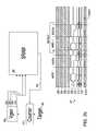
- the chip ( 620 ) and system ( 600 ) architecture and a flow chart employing RICID with a fuzzy algorithmare shown.
- the chipis assumed to consist of 128 Kb eDRAM array ( 621 ) with 32 4 Kb segments ( 626 ) numbered (0, 0) to (7,3). They are supported by a BIST ( 625 ), wordline low voltage (VWL) generator ( 622 ), RICID generator (ID GEN ) ( 624 ), and segment manager (SEG) ( 623 ).
- VWLwordline low voltage
- RICID generatorID GEN
- SEGsegment manager
- the systemincludes a module ( 602 ) that requests an RICID with a given KEY ( 610 ) and expects an RICID ( 611 ) response. It further includes the capability to store the RICID in the table ( 601 ) RICID TBL .
- the systemprovides the chip with two fixed keys ( 602 ), KEY MIN and KEY MAX , which are, respectively, minimum and maximum numbers of the retention fails expected in an RICID string.
- the chipreceives ID requests ( 610 )
- the BIST ( 625 )changes VWL ( 622 ) so that KEY MIN ⁇ the number of RICID ⁇ KEY MIN +GB for the first segment (1,1). If the chip does not satisfy this condition, BIST selects the next segment (2,1) using SEG ( 623 ).
- the vector RICID MINis temporarily stored by the BIST, and the BIST initiates a search for the vector RICID MAX using the second value KEY MAX by changing VWL to satisfy KEY MAX ⁇ GB ⁇ number of RICID ⁇ KEY MAX . Verification is achieved by confirming that the vector RICID MIN is a subset of RICID MAX . Otherwise, the vectors are deemed unreliable, the improper condition is detected by the BIST, and the segment is incremented by SEG to search for new RICID MIN and RICID MAX vectors using the aforementioned VWL tuning previously described to be applied to the next segment.
- the vectorsare compressed by ID GEN ( 624 ) and are outputted to the system as a RICID ( 611 ).
- the RICID vectoris then compared with existing RICID TBL vectors in an RICID table ( 601 ), if available, to confirm that it is a unique ID. Else, the system requests a new RICID pair by requiring the BIST to increment the segment selection SEG.
- the unique RICIDis preferably stored in a table by the manufacturer. More generally, SEG may optionally be stored in an eFUSE or in a table.
- the RICID read operationis enabled by providing the read key KEY R to the chip at KEY ( 610 ).
- KEY Ris dynamically changed at each read operation. Two adjacent KEY R values should be more than two GBs apart, permitting a correct detection even if unstable bits change within a boundary.
- the systemchecks if the number of 1 bits in RICID R is equal to the quantity KEY R input by the system within the tolerance of GB, in order to prevent an illegal key readout, such as a previous key that a counterfeit may have preprogrammed. If the quantity is valid, RICID R is compared against the table of RICIDs stored by the foundry or OEM to find RICID MAX , of which the given RICID R is a subset.
- FIG. 8a table defining terms relevant to RICID generation, detection, and storage is illustrated.
- the input to the chipis KEY
- the output from the chipis RICID
- the stored valueis RICID-TBL.
- the KEY values providedare KEY MIN and KEY MAX , which describe the minimum and maximum number of 1 bits permitted in the ID string, subject to a GB
- the RICID response valuesare, respectively, RICID MIN and RICID MAX
- the resulting stored RICID TBL valuesare RICID MIN and RICID MAX .
- the value KEY Ris input to the chip, and the response is RICID R , which is compared to, and expected to be a subset of, RICID MAX stored in RICID TBL .
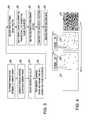
- a flow chart illustrating the steps for RICID generationis depicted, including a particular manner in which a suitable RICID may be found.
- the chip ( 800 ) inputreceives KEY MIN and KEY MAX .
- An initial test conditionis applied to a segment of the memory array with the expectation that the array will have no failing cells ( 801 ). If it does, a different segment must be selected ( 807 ). Otherwise, the VWL level (or other suitable test parameter) is changed ( 802 ) until the number of fails occurring on the chip is greater than or equal to KEY MIN but less than KEY MIN +GB ( 803 ). Failing cell addresses are recorded temporarily as RICID MIN .
- the VWL level(or other suitable test parameter) is further changed ( 804 ) until the number of failing cells occurring on the chip is greater than or equal to KEY MAX ⁇ GB but less than or equal to KEY MAX .
- Failing cell addressesare recorded temporarily as RICID MAX . If RICID MAX includes RICID MIN ( 806 ), the RICID MIN and RICID MAX values are output to the system ( 810 ). If RICID MAX does not include RICID MIN , the segment is incremented to the next suitable position ( 813 ), and the process is repeated starting from 801 . If no suitable segments are available, an error is reported ( 820 ) and no chip ID can be recorded by this scheme due to unsuitable hardware.
- RICID MIN and RICID MAXare compared to the list of existing recorded RICID values in a table ( 811 ). If they are unique among the group of devices fabricated to given specifications, then the RICID values are stored in a table ( 812 ) by the manufacturer or OEM.
- FIG. 10a flow chart illustrating steps for an RICID reading is shown, including the specific manner in which a suitable RICID may be found.
- the chip ( 900 ) inputreceives KEY R .
- An initial test conditionis applied to the segment from which the RICID was originally collected with the expectation that the array will have no failing cells ( 901 ). If it does, the chip is damaged and an RICID cannot be read, so an error is reported ( 920 ). If it does not, the VWL level (or other suitable test parameter) is changed ( 902 ) until the number of fails occurring on the chip is nearly equal to KEY R , within GB of KEY R either greater or less ( 903 ).
- the failing cell addressesare output from the chip as RICID R ( 911 ).
- the system ( 910 )receives RICID R and checks if the number of failing bits reported in RICID R is close to KEY R and within GB ( 912 ). If it is not, the chip is not valid and an error is reported ( 920 ). Next, the table of RICID values RICID TBL is searched for a stored RICID MAX value that includes RICID R ( 913 ).
- the chipis not a member of the group of devices and may be counterfeit, or it may be of an unknown source, or otherwise be invalid, in which case an error is reported ( 920 ). Otherwise, the RICID R matches with a value in the table and the chip is successfully identified ( 914 ).
- the illustrative chip presently usedis assumed to not have a BIST or a built-in VWL adjustment function. However, they can be emulated by ATE communicating by way of the memory array in DMA mode.
- RICIDsare preferably collected for 32 eDRAM arrays by incrementing the VWL value applied to the memory array in 2 mV steps to collect a predetermined number of fails. For the present illustrative demonstration, an array area of 4 Kb is selected.
- the RICID having at most 100 bits within the 15% GBwas collected from each chip by moving the VWL value and RICID was verified for the selected array area by confirming that obtaining 10 failing bits from the chip and confirming that the same failures occurring in the original RICID.
- the chipsare identified using sample KEY R requests of 25, 50, and 75. Using these inputs to the simulated BIST, it confirms that the chips can be uniquely identified using a subset of the original recorded RICID TBL .
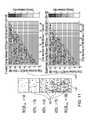
- FIG. 11the hardware results for 32 chips are illustrated.
- the collection of bit maps for a single chip across varying ID sizes ( 1101 )shows failures traced ( 1102 ) from one ID to the next for a 4 Kb area.
- Hamming distance distributionsare illustrated for all pairs of RICID MAX vectors which were generated by Monte Carlo simulation ( 1201 ) and experimentally using hardware ( 1202 ). Both sets of vectors preferably had j ranging from 86 to 100 and a mean number of fails equal to 94.8 for RICID. Mean and ⁇ of the Hamming distance were 94.7 and 2.8 for simulated results and 94.6 and 3.0 for experimental results. Distances are normally distributed within 95% confidence limits in normal quantile plots.
- the present inventioncan be realized in hardware, software, or a combination of hardware and software.
- the inventioncan be realized in a centralized fashion in one computer system or in a distributed fashion where different elements are spread across several interconnected computer systems. Any kind of computer system—or other apparatus adapted for carrying out the methods described herein—is suitable.
- a typical combination of hardware and softwarecould be a general purpose computer system with a computer program that, when being loaded and executed, controls the computer system such that it carries out the methods described herein.
- the present inventioncan also be embedded in a computer program product, which comprises all the features enabling the implementation of the methods described herein, and which—when loaded in a computer system—is able to carry out these methods.
- Computer program means or computer program in the present contextmean any expression, in any language, code or notation, of a set of instructions intended to cause a system having an information processing capability to perform a particular function either directly or after conversion to another language, code or notation and/or reproduction in a different material form.
Landscapes
- Engineering & Computer Science (AREA)
- Theoretical Computer Science (AREA)
- Computer Security & Cryptography (AREA)
- Physics & Mathematics (AREA)
- Computer Hardware Design (AREA)
- General Physics & Mathematics (AREA)
- Software Systems (AREA)
- General Engineering & Computer Science (AREA)
- Mathematical Physics (AREA)
- Computer Networks & Wireless Communication (AREA)
- Signal Processing (AREA)
- Storage Device Security (AREA)
- Tests Of Electronic Circuits (AREA)
- Collating Specific Patterns (AREA)
- Lock And Its Accessories (AREA)
- Static Random-Access Memory (AREA)
- Dram (AREA)
- Semiconductor Integrated Circuits (AREA)
- For Increasing The Reliability Of Semiconductor Memories (AREA)
Abstract
Description
Claims (13)
Priority Applications (9)
| Application Number | Priority Date | Filing Date | Title |
|---|---|---|---|
| US13/302,314US8590010B2 (en) | 2011-11-22 | 2011-11-22 | Retention based intrinsic fingerprint identification featuring a fuzzy algorithm and a dynamic key |
| BR112014012103ABR112014012103A2 (en) | 2011-11-22 | 2012-09-13 | intrinsic memory arrangement chip identification method and non-readable storage program device by intrinsic memory arrangement chip identification method and non-transient machine read storage program device for performing such method |
| CA2852883ACA2852883A1 (en) | 2011-11-22 | 2012-09-13 | Retention based intrinsic fingerprint identification featuring a fuzzy algorithm and a dynamic key |
| JP2014542305AJP2015504634A (en) | 2011-11-22 | 2012-09-13 | Retention-based unique fingerprint identification featuring fuzzy algorithms and dynamic keys |
| PCT/US2012/055061WO2013077929A2 (en) | 2011-11-22 | 2012-09-13 | Retention based intrinsic fingerprint identification featuring a fuzzy algorithm and a dynamic key |
| GB1404456.4AGB2508761B (en) | 2011-11-22 | 2012-09-13 | Retention Based Intrinsic Fingerprint Identification Featuring a Fuzzy Algorithm and a Dynamic Key |
| IN2203CHN2014IN2014CN02203A (en) | 2011-11-22 | 2012-09-13 | |
| DE112012004439.8TDE112012004439B4 (en) | 2011-11-22 | 2012-09-13 | Memory-based intrinsic fingerprint identification with a fuzzy algorithm and a dynamic key |
| CN201280057317.8ACN103946854B (en) | 2011-11-22 | 2012-09-13 | The intrinsic fingerprint recognition based on reservation being characterized with fuzzy algorithmic approach and dynamic key |
Applications Claiming Priority (1)
| Application Number | Priority Date | Filing Date | Title |
|---|---|---|---|
| US13/302,314US8590010B2 (en) | 2011-11-22 | 2011-11-22 | Retention based intrinsic fingerprint identification featuring a fuzzy algorithm and a dynamic key |
Publications (2)
| Publication Number | Publication Date |
|---|---|
| US20130133031A1 US20130133031A1 (en) | 2013-05-23 |
| US8590010B2true US8590010B2 (en) | 2013-11-19 |
Family
ID=48428263
Family Applications (1)
| Application Number | Title | Priority Date | Filing Date |
|---|---|---|---|
| US13/302,314ActiveUS8590010B2 (en) | 2011-11-22 | 2011-11-22 | Retention based intrinsic fingerprint identification featuring a fuzzy algorithm and a dynamic key |
Country Status (9)
| Country | Link |
|---|---|
| US (1) | US8590010B2 (en) |
| JP (1) | JP2015504634A (en) |
| CN (1) | CN103946854B (en) |
| BR (1) | BR112014012103A2 (en) |
| CA (1) | CA2852883A1 (en) |
| DE (1) | DE112012004439B4 (en) |
| GB (1) | GB2508761B (en) |
| IN (1) | IN2014CN02203A (en) |
| WO (1) | WO2013077929A2 (en) |
Cited By (8)
| Publication number | Priority date | Publication date | Assignee | Title |
|---|---|---|---|---|
| US20150098268A1 (en)* | 2013-10-04 | 2015-04-09 | Renesas Electronics Corporation | Semiconductor memory |
| US9038133B2 (en)* | 2012-12-07 | 2015-05-19 | International Business Machines Corporation | Self-authenticating of chip based on intrinsic features |
| US20150260786A1 (en)* | 2014-03-11 | 2015-09-17 | Cryptography Research, Inc. | Integrated circuit authentication |
| US9390291B2 (en)* | 2012-12-29 | 2016-07-12 | Intel Corporation | Secure key derivation and cryptography logic for integrated circuits |
| US9436845B2 (en) | 2014-03-25 | 2016-09-06 | Globalfoundries Inc. | Physically unclonable fuse using a NOR type memory array |
| US9608827B1 (en)* | 2016-01-18 | 2017-03-28 | Xilinx, Inc. | Memory cell with de-initialization circuitry |
| US20240185906A1 (en)* | 2021-11-30 | 2024-06-06 | Samsung Electronics Co., Ltd. | Semiconductor memory device and memory system having the same |
| US12407532B2 (en) | 2020-02-18 | 2025-09-02 | International Business Machines Corporation | Gain cell memory based physically unclonable function |
Families Citing this family (20)
| Publication number | Priority date | Publication date | Assignee | Title |
|---|---|---|---|---|
| JP5873762B2 (en)* | 2012-05-29 | 2016-03-01 | ルネサスエレクトロニクス株式会社 | Semiconductor device and method for generating identification information of semiconductor device |
| US20140282925A1 (en)* | 2013-03-15 | 2014-09-18 | Sypris Electronics, Llc | Personal Authentication Device and System for Securing Transactions on a Mobile Device |
| JP6106043B2 (en)* | 2013-07-25 | 2017-03-29 | ルネサスエレクトロニクス株式会社 | Semiconductor integrated circuit device |
| US9219722B2 (en)* | 2013-12-11 | 2015-12-22 | Globalfoundries Inc. | Unclonable ID based chip-to-chip communication |
| US9224030B2 (en)* | 2014-01-10 | 2015-12-29 | Qualcomm Incorporated | Sensor identification |
| US10218517B2 (en)* | 2014-03-25 | 2019-02-26 | Carnegie Mellon University | Methods for generating reliable responses in physical unclonable functions (PUFs) and methods for designing strong PUFs |
| US9497027B2 (en)* | 2014-06-02 | 2016-11-15 | GlobalFoundries, Inc. | Encryption engine with twin cell memory array |
| FR3038411B1 (en)* | 2015-06-30 | 2018-08-17 | Stmicroelectronics (Rousset) Sas | DETECTION OF AUTHENTICITY OF AN ELECTRONIC CIRCUIT OR A PRODUCT CONTAINING SUCH A CIRCUIT |
| US9401222B1 (en) | 2015-11-23 | 2016-07-26 | International Business Machines Corporation | Determining categories for memory fail conditions |
| EP3403209B1 (en)* | 2016-01-11 | 2024-04-24 | UNM Rainforest Innovations | A privacy-preserving, mutual puf-based authentication protocol |
| US10515710B2 (en)* | 2016-11-28 | 2019-12-24 | Taiwan Semiconductor Manufacturing Co., Ltd. | Hamming-distance analyzer |
| US10515713B2 (en) | 2016-11-28 | 2019-12-24 | Taiwan Semiconductor Manufacturing Co., Ltd. | Hamming-distance analyzer and method for analyzing hamming-distance |
| WO2018122235A1 (en)* | 2016-12-30 | 2018-07-05 | Robert Bosch Gmbh | Reverse computational fuzzy extractor and method for authentication |
| WO2018145755A1 (en)* | 2017-02-10 | 2018-08-16 | Telefonaktiebolaget Lm Ericsson (Publ) | Methods of verifying that a first device and a second device are physically interconnected |
| DE102017205818A1 (en)* | 2017-04-05 | 2018-10-11 | Robert Bosch Gmbh | Adjustable physical unclonable function |
| US10840157B2 (en)* | 2017-06-02 | 2020-11-17 | University of Viriginia Patent Foundation | Methods for reducing chip testing time using trans-threshold correlations |
| US10652032B2 (en)* | 2017-06-20 | 2020-05-12 | Taiwan Semiconductor Manufacturing Company, Ltd. | Device signature generation |
| US10811073B2 (en)* | 2018-04-25 | 2020-10-20 | Birad—Research & Development Company Ltd. | Dynamic memory physical unclonable function |
| US11269999B2 (en)* | 2019-07-01 | 2022-03-08 | At&T Intellectual Property I, L.P. | Protecting computing devices from malicious tampering |
| US11621036B2 (en)* | 2020-07-14 | 2023-04-04 | Taiwan Semiconductor Manufacturing Company, Ltd. | Method of operating an integrated circuit and integrated circuit |
Citations (23)
| Publication number | Priority date | Publication date | Assignee | Title |
|---|---|---|---|---|
| US5051374A (en)* | 1985-03-06 | 1991-09-24 | Sharp Kabushiki Kaisha | Method of manufacturing a semiconductor device with identification pattern |
| US5617531A (en)* | 1993-11-02 | 1997-04-01 | Motorola, Inc. | Data Processor having a built-in internal self test controller for testing a plurality of memories internal to the data processor |
| US6161213A (en)* | 1999-02-17 | 2000-12-12 | Icid, Llc | System for providing an integrated circuit with a unique identification |
| US20020024905A1 (en) | 2000-08-24 | 2002-02-28 | Kahlman Josephus Arnoldus Henricus Maria | Copy Protection of optical discs comprising a chip |
| US6367042B1 (en)* | 1998-12-11 | 2002-04-02 | Lsi Logic Corporation | Testing methodology for embedded memories using built-in self repair and identification circuitry |
| US6403251B1 (en)* | 2000-01-31 | 2002-06-11 | Moltech Power Systems, Inc | Battery pack with multiple secure modules |
| US20030204743A1 (en)* | 2002-04-16 | 2003-10-30 | Srinivas Devadas | Authentication of integrated circuits |
| US20070018677A1 (en)* | 2002-07-29 | 2007-01-25 | Marr Kenneth W | Methods for wafer level burn-in |
| US20090011596A1 (en)* | 2004-12-17 | 2009-01-08 | Matsushita Electric Industrial Co., Ltd. | Electronic device and manufacturing method thereof |
| US20090138772A1 (en)* | 2007-10-18 | 2009-05-28 | The Regents Of The University Of Michigan | Microprocessor and method for detecting faults therein |
| US20090326840A1 (en)* | 2008-06-26 | 2009-12-31 | International Business Machines Corporation | Temperature-Profiled Device Fingerprint Generation and Authentication from Power-Up States of Static Cells |
| US20100097843A1 (en)* | 2002-02-11 | 2010-04-22 | Stmicroelectronics S.A. | Extraction of a binary code based on physical parameters of an integrated circuit |
| US20100176920A1 (en) | 2007-06-14 | 2010-07-15 | Intrinsic Id Bv | Method and device for providing digital security |
| US20100306832A1 (en) | 2009-05-27 | 2010-12-02 | Ruicao Mu | Method for fingerprinting and identifying internet users |
| US7945791B2 (en)* | 2001-06-11 | 2011-05-17 | Stmicroelectronics S.A. | Protected storage of a datum in an integrated circuit |
| WO2011089143A1 (en) | 2010-01-20 | 2011-07-28 | Intrinsic Id B.V. | Device and method for obtaining a cryptographic key |
| US20110215829A1 (en) | 2007-08-22 | 2011-09-08 | Intrinsic Id B.V. | Identification of devices using physically unclonable functions |
| US20110234241A1 (en)* | 2009-02-23 | 2011-09-29 | Lewis James M | Method and system for protecting products and technology from integrated circuits which have been subject to tampering, stressing and replacement as well as detecting integrated circuits that have been subject to tampering |
| US20120159276A1 (en)* | 2010-12-16 | 2012-06-21 | University Of Southern California | Automated detection of and compensation for guardband degradation during operation of clocked data processing circuit |
| US20120179952A1 (en)* | 2009-08-14 | 2012-07-12 | Pim Theo Tuyls | Physically unclonable function with tamper prevention and anti-aging system |
| US20120183135A1 (en)* | 2011-01-19 | 2012-07-19 | Verayo, Inc. | Reliable puf value generation by pattern matching |
| US20120230087A1 (en)* | 2011-03-08 | 2012-09-13 | Arizona Technology Enterprises, Llc | Sram circuits for circuit identification using a digital fingerprint |
| US20120243310A1 (en)* | 2011-03-21 | 2012-09-27 | Skymedi Corporation | Method of programming a multi-bit per cell non-volatile memory |
Family Cites Families (6)
| Publication number | Priority date | Publication date | Assignee | Title |
|---|---|---|---|---|
| WO2006053304A2 (en)* | 2004-11-12 | 2006-05-18 | Pufco, Inc. | Volatile device keys and applications thereof |
| RU2007144715A (en)* | 2005-06-01 | 2009-06-10 | Конинклейке Филипс Электроникс Н.В. (Nl) | UPDATE TEMPLATE IN ASSISTANT DATA SYSTEMS |
| EP2081170A1 (en)* | 2006-11-06 | 2009-07-22 | Panasonic Corporation | Information security apparatus |
| US7701801B2 (en)* | 2007-06-12 | 2010-04-20 | International Business Machines Corporation | Programmable pulsewidth and delay generating circuit for integrated circuits |
| EP2214117B1 (en)* | 2007-09-19 | 2012-02-01 | Verayo, Inc. | Authentication with physical unclonable functions |
| WO2009128044A1 (en)* | 2008-04-17 | 2009-10-22 | Koninklijke Philips Electronics N.V. | Method of reducing the occurrence of burn-in due to negative bias temperature instability |
- 2011
- 2011-11-22USUS13/302,314patent/US8590010B2/enactiveActive
- 2012
- 2012-09-13CNCN201280057317.8Apatent/CN103946854B/ennot_activeExpired - Fee Related
- 2012-09-13CACA2852883Apatent/CA2852883A1/ennot_activeAbandoned
- 2012-09-13GBGB1404456.4Apatent/GB2508761B/ennot_activeExpired - Fee Related
- 2012-09-13ININ2203CHN2014patent/IN2014CN02203A/enunknown
- 2012-09-13JPJP2014542305Apatent/JP2015504634A/enactivePending
- 2012-09-13WOPCT/US2012/055061patent/WO2013077929A2/enactiveApplication Filing
- 2012-09-13BRBR112014012103Apatent/BR112014012103A2/ennot_activeIP Right Cessation
- 2012-09-13DEDE112012004439.8Tpatent/DE112012004439B4/ennot_activeExpired - Fee Related
Patent Citations (33)
| Publication number | Priority date | Publication date | Assignee | Title |
|---|---|---|---|---|
| US5051374A (en)* | 1985-03-06 | 1991-09-24 | Sharp Kabushiki Kaisha | Method of manufacturing a semiconductor device with identification pattern |
| US5617531A (en)* | 1993-11-02 | 1997-04-01 | Motorola, Inc. | Data Processor having a built-in internal self test controller for testing a plurality of memories internal to the data processor |
| US6367042B1 (en)* | 1998-12-11 | 2002-04-02 | Lsi Logic Corporation | Testing methodology for embedded memories using built-in self repair and identification circuitry |
| USRE40188E1 (en)* | 1999-02-17 | 2008-03-25 | Icid, Llc | System and method for providing an integrated circuit with a unique identification |
| US6161213A (en)* | 1999-02-17 | 2000-12-12 | Icid, Llc | System for providing an integrated circuit with a unique identification |
| US6403251B1 (en)* | 2000-01-31 | 2002-06-11 | Moltech Power Systems, Inc | Battery pack with multiple secure modules |
| US20020024905A1 (en) | 2000-08-24 | 2002-02-28 | Kahlman Josephus Arnoldus Henricus Maria | Copy Protection of optical discs comprising a chip |
| US7945791B2 (en)* | 2001-06-11 | 2011-05-17 | Stmicroelectronics S.A. | Protected storage of a datum in an integrated circuit |
| US20100097843A1 (en)* | 2002-02-11 | 2010-04-22 | Stmicroelectronics S.A. | Extraction of a binary code based on physical parameters of an integrated circuit |
| US20060271793A1 (en)* | 2002-04-16 | 2006-11-30 | Srinivas Devadas | Reliable generation of a device-specific value |
| US20070183194A1 (en)* | 2002-04-16 | 2007-08-09 | Srinivas Devadas | Controlling access to device-specific information |
| US20060271792A1 (en)* | 2002-04-16 | 2006-11-30 | Srinivas Devadas | Data protection and cryptographic functions using a device-specific value |
| US20060221686A1 (en)* | 2002-04-16 | 2006-10-05 | Srinivas Devadas | Integrated circuit that uses a dynamic characteristic of the circuit |
| US7757083B2 (en)* | 2002-04-16 | 2010-07-13 | Massachusetts Institute Of Technology | Integrated circuit that uses a dynamic characteristic of the circuit |
| US7840803B2 (en) | 2002-04-16 | 2010-11-23 | Massachusetts Institute Of Technology | Authentication of integrated circuits |
| US20120033810A1 (en)* | 2002-04-16 | 2012-02-09 | Massachusetts Institute Of Technology | Authentication of integrated circuits |
| US20030204743A1 (en)* | 2002-04-16 | 2003-10-30 | Srinivas Devadas | Authentication of integrated circuits |
| US20070018677A1 (en)* | 2002-07-29 | 2007-01-25 | Marr Kenneth W | Methods for wafer level burn-in |
| US20090011596A1 (en)* | 2004-12-17 | 2009-01-08 | Matsushita Electric Industrial Co., Ltd. | Electronic device and manufacturing method thereof |
| US20100176920A1 (en) | 2007-06-14 | 2010-07-15 | Intrinsic Id Bv | Method and device for providing digital security |
| US20110215829A1 (en) | 2007-08-22 | 2011-09-08 | Intrinsic Id B.V. | Identification of devices using physically unclonable functions |
| US20090138772A1 (en)* | 2007-10-18 | 2009-05-28 | The Regents Of The University Of Michigan | Microprocessor and method for detecting faults therein |
| US20090326840A1 (en)* | 2008-06-26 | 2009-12-31 | International Business Machines Corporation | Temperature-Profiled Device Fingerprint Generation and Authentication from Power-Up States of Static Cells |
| US8219857B2 (en)* | 2008-06-26 | 2012-07-10 | International Business Machines Corporation | Temperature-profiled device fingerprint generation and authentication from power-up states of static cells |
| US20120246494A1 (en)* | 2008-06-26 | 2012-09-27 | International Business Machines Corporation | Temperature-profiled device fingerprint generation and authentication from power-up states of static cells |
| US20110234241A1 (en)* | 2009-02-23 | 2011-09-29 | Lewis James M | Method and system for protecting products and technology from integrated circuits which have been subject to tampering, stressing and replacement as well as detecting integrated circuits that have been subject to tampering |
| US20100306832A1 (en) | 2009-05-27 | 2010-12-02 | Ruicao Mu | Method for fingerprinting and identifying internet users |
| US20120179952A1 (en)* | 2009-08-14 | 2012-07-12 | Pim Theo Tuyls | Physically unclonable function with tamper prevention and anti-aging system |
| WO2011089143A1 (en) | 2010-01-20 | 2011-07-28 | Intrinsic Id B.V. | Device and method for obtaining a cryptographic key |
| US20120159276A1 (en)* | 2010-12-16 | 2012-06-21 | University Of Southern California | Automated detection of and compensation for guardband degradation during operation of clocked data processing circuit |
| US20120183135A1 (en)* | 2011-01-19 | 2012-07-19 | Verayo, Inc. | Reliable puf value generation by pattern matching |
| US20120230087A1 (en)* | 2011-03-08 | 2012-09-13 | Arizona Technology Enterprises, Llc | Sram circuits for circuit identification using a digital fingerprint |
| US20120243310A1 (en)* | 2011-03-21 | 2012-09-27 | Skymedi Corporation | Method of programming a multi-bit per cell non-volatile memory |
Non-Patent Citations (7)
| Title |
|---|
| "A Chip-ID Generating Circuit for Dependable LSI Using Random Address Errors on Embedded SRAM and On-Chip Memory BIST", H. Fujiwara, et al., 2011 Symposium on VLSI Circuits Digest of Technical Papers. |
| "A Digita 1.6 pJ/bit Chip Identification Circuit Using Process Variations", Y. Su, et al., IEEE Journal of Solid-State Circuits, vol. 43, No. 1, Jan. 2008. |
| International Search Report/Written Opinion; PCT/US2012/055061; May 16, 2013. |
| Maximilian Hofer & Christoph Boehm, An Alternative to Error Correction for SRAM-Like PUFS, Proceedings of the 12th International Conference on Cryptographic Hardware and Embedded Systems (CHES) 335-350 (2010).* |
| Science and Technology Information Center Search Strategy Report including terms searched, list of patents and non-patent literature (Jun. 19, 2013).* |
| Taniya Siddiqua, A Multi-Level Approach to Reduce the Impact of NBTI on Processor Functional Units, Greater Lakes Symposium on VLSI (May 16-18, 2010).* |
| Y. Su et al., A 1.6pJ/bit 96% Stable Chip-ID Generating Circuit using Process Variations, IEEE International Solid-State Circuits Conference (2007).* |
Cited By (15)
| Publication number | Priority date | Publication date | Assignee | Title |
|---|---|---|---|---|
| US9690927B2 (en) | 2012-12-07 | 2017-06-27 | International Business Machines Corporation | Providing an authenticating service of a chip |
| US9038133B2 (en)* | 2012-12-07 | 2015-05-19 | International Business Machines Corporation | Self-authenticating of chip based on intrinsic features |
| US11210373B2 (en) | 2012-12-07 | 2021-12-28 | International Business Machines Corporation | Authenticating a hardware chip using an intrinsic chip identifier |
| US10657231B2 (en) | 2012-12-07 | 2020-05-19 | International Business Machines Corporation | Providing an authenticating service of a chip |
| US10262119B2 (en) | 2012-12-07 | 2019-04-16 | International Business Machines Corporation | Providing an authenticating service of a chip |
| US9390291B2 (en)* | 2012-12-29 | 2016-07-12 | Intel Corporation | Secure key derivation and cryptography logic for integrated circuits |
| US9443575B2 (en)* | 2013-10-04 | 2016-09-13 | Renesas Electronics Corporation | Semiconductor memory |
| US20150098268A1 (en)* | 2013-10-04 | 2015-04-09 | Renesas Electronics Corporation | Semiconductor memory |
| US9970986B2 (en)* | 2014-03-11 | 2018-05-15 | Cryptography Research, Inc. | Integrated circuit authentication |
| US20150260786A1 (en)* | 2014-03-11 | 2015-09-17 | Cryptography Research, Inc. | Integrated circuit authentication |
| US9436845B2 (en) | 2014-03-25 | 2016-09-06 | Globalfoundries Inc. | Physically unclonable fuse using a NOR type memory array |
| US9608827B1 (en)* | 2016-01-18 | 2017-03-28 | Xilinx, Inc. | Memory cell with de-initialization circuitry |
| US12407532B2 (en) | 2020-02-18 | 2025-09-02 | International Business Machines Corporation | Gain cell memory based physically unclonable function |
| US20240185906A1 (en)* | 2021-11-30 | 2024-06-06 | Samsung Electronics Co., Ltd. | Semiconductor memory device and memory system having the same |
| US12236994B2 (en)* | 2021-11-30 | 2025-02-25 | Samsung Electronics Co., Ltd. | Semiconductor memory device and memory system having the same |
Also Published As
| Publication number | Publication date |
|---|---|
| GB2508761B (en) | 2014-11-19 |
| CN103946854B (en) | 2016-08-24 |
| CA2852883A1 (en) | 2013-05-30 |
| IN2014CN02203A (en) | 2015-06-12 |
| DE112012004439B4 (en) | 2016-11-24 |
| GB201404456D0 (en) | 2014-04-30 |
| JP2015504634A (en) | 2015-02-12 |
| CN103946854A (en) | 2014-07-23 |
| WO2013077929A3 (en) | 2013-08-15 |
| DE112012004439T5 (en) | 2014-07-17 |
| BR112014012103A2 (en) | 2017-05-30 |
| US20130133031A1 (en) | 2013-05-23 |
| WO2013077929A2 (en) | 2013-05-30 |
| GB2508761A (en) | 2014-06-11 |
Similar Documents
| Publication | Publication Date | Title |
|---|---|---|
| US8590010B2 (en) | Retention based intrinsic fingerprint identification featuring a fuzzy algorithm and a dynamic key | |
| US12050495B2 (en) | Methods and apparatus to create a physically unclonable function | |
| US11210373B2 (en) | Authenticating a hardware chip using an intrinsic chip identifier | |
| US12244741B2 (en) | Physical unclonable function (PUF) security key generation | |
| US10038564B2 (en) | Physical unclonable function using augmented memory for challenge-response hashing | |
| Talukder et al. | PreLatPUF: Exploiting DRAM latency variations for generating robust device signatures | |
| Holcomb et al. | Bitline PUF: building native challenge-response PUF capability into any SRAM | |
| JP6063679B2 (en) | Semiconductor device | |
| JP6793044B2 (en) | Non-volatile memory device | |
| Tang et al. | A DRAM based physical unclonable function capable of generating> 10 32 Challenge Response Pairs per 1Kbit array for secure chip authentication | |
| Yue et al. | DRAM-based authentication using deep convolutional neural networks | |
| CN115668196A (en) | Device, system and method for device identification based on fuse array | |
| Müelich et al. | Channel models for physical unclonable functions based on DRAM retention measurements | |
| WO2020128547A1 (en) | Method and device to ensure a secure memory access | |
| Kirihata et al. | 17 Dynamic Intrinsic Chip ID for Hardware Security | |
| Tehranipoor et al. | Volatile Memory-Based PUF | |
| Kumar et al. | Physically unclonable functions: A window into CMOS process variations | |
| Kirihata et al. | 17 Dynamic Intrinsic Chip | |
| Nii | SRAM-Based Physical Unclonable Functions (PUFs) to Generate Signature Out of Silicon for Authentication and Encryption | |
| Holcomb | Nanoscale CMOS Memory-Based Security Primitive Design |
Legal Events
| Date | Code | Title | Description |
|---|---|---|---|
| AS | Assignment | Owner name:INTERNATIONAL BUSINESS MACHINES CORPORATION, NEW Y Free format text:ASSIGNMENT OF ASSIGNORS INTEREST;ASSIGNORS:FAINSTEIN, DANIEL J.;CESTERO, ALBERTO;IYER, SUBRAMANIAN S.;AND OTHERS;SIGNING DATES FROM 20111116 TO 20111117;REEL/FRAME:027265/0471 | |
| STCF | Information on status: patent grant | Free format text:PATENTED CASE | |
| AS | Assignment | Owner name:GLOBALFOUNDRIES U.S. 2 LLC, NEW YORK Free format text:ASSIGNMENT OF ASSIGNORS INTEREST;ASSIGNOR:INTERNATIONAL BUSINESS MACHINES CORPORATION;REEL/FRAME:036550/0001 Effective date:20150629 | |
| AS | Assignment | Owner name:GLOBALFOUNDRIES INC., CAYMAN ISLANDS Free format text:ASSIGNMENT OF ASSIGNORS INTEREST;ASSIGNORS:GLOBALFOUNDRIES U.S. 2 LLC;GLOBALFOUNDRIES U.S. INC.;REEL/FRAME:036779/0001 Effective date:20150910 | |
| FPAY | Fee payment | Year of fee payment:4 | |
| AS | Assignment | Owner name:WILMINGTON TRUST, NATIONAL ASSOCIATION, DELAWARE Free format text:SECURITY AGREEMENT;ASSIGNOR:GLOBALFOUNDRIES INC.;REEL/FRAME:049490/0001 Effective date:20181127 | |
| AS | Assignment | Owner name:GLOBALFOUNDRIES U.S. INC., CALIFORNIA Free format text:ASSIGNMENT OF ASSIGNORS INTEREST;ASSIGNOR:GLOBALFOUNDRIES INC.;REEL/FRAME:050122/0001 Effective date:20190821 | |
| AS | Assignment | Owner name:MARVELL INTERNATIONAL LTD., BERMUDA Free format text:ASSIGNMENT OF ASSIGNORS INTEREST;ASSIGNOR:GLOBALFOUNDRIES U.S. INC.;REEL/FRAME:051070/0625 Effective date:20191105 | |
| AS | Assignment | Owner name:CAVIUM INTERNATIONAL, CAYMAN ISLANDS Free format text:ASSIGNMENT OF ASSIGNORS INTEREST;ASSIGNOR:MARVELL INTERNATIONAL LTD.;REEL/FRAME:052918/0001 Effective date:20191231 | |
| AS | Assignment | Owner name:MARVELL ASIA PTE, LTD., SINGAPORE Free format text:ASSIGNMENT OF ASSIGNORS INTEREST;ASSIGNOR:CAVIUM INTERNATIONAL;REEL/FRAME:053475/0001 Effective date:20191231 | |
| AS | Assignment | Owner name:GLOBALFOUNDRIES INC., CAYMAN ISLANDS Free format text:RELEASE BY SECURED PARTY;ASSIGNOR:WILMINGTON TRUST, NATIONAL ASSOCIATION;REEL/FRAME:054636/0001 Effective date:20201117 | |
| MAFP | Maintenance fee payment | Free format text:PAYMENT OF MAINTENANCE FEE, 8TH YEAR, LARGE ENTITY (ORIGINAL EVENT CODE: M1552); ENTITY STATUS OF PATENT OWNER: LARGE ENTITY Year of fee payment:8 | |
| MAFP | Maintenance fee payment | Free format text:PAYMENT OF MAINTENANCE FEE, 12TH YEAR, LARGE ENTITY (ORIGINAL EVENT CODE: M1553); ENTITY STATUS OF PATENT OWNER: LARGE ENTITY Year of fee payment:12 |