US8587915B2 - Arrangement for energy conditioning - Google Patents
Arrangement for energy conditioningDownload PDFInfo
- Publication number
- US8587915B2 US8587915B2US13/195,495US201113195495AUS8587915B2US 8587915 B2US8587915 B2US 8587915B2US 201113195495 AUS201113195495 AUS 201113195495AUS 8587915 B2US8587915 B2US 8587915B2
- Authority
- US
- United States
- Prior art keywords
- conductor
- electrode
- surface area
- superposed
- energy
- Prior art date
- Legal status (The legal status is an assumption and is not a legal conclusion. Google has not performed a legal analysis and makes no representation as to the accuracy of the status listed.)
- Expired - Fee Related
Links
Images


Classifications
- H—ELECTRICITY
- H05—ELECTRIC TECHNIQUES NOT OTHERWISE PROVIDED FOR
- H05K—PRINTED CIRCUITS; CASINGS OR CONSTRUCTIONAL DETAILS OF ELECTRIC APPARATUS; MANUFACTURE OF ASSEMBLAGES OF ELECTRICAL COMPONENTS
- H05K9/00—Screening of apparatus or components against electric or magnetic fields
- H—ELECTRICITY
- H01—ELECTRIC ELEMENTS
- H01L—SEMICONDUCTOR DEVICES NOT COVERED BY CLASS H10
- H01L23/00—Details of semiconductor or other solid state devices
- H01L23/48—Arrangements for conducting electric current to or from the solid state body in operation, e.g. leads, terminal arrangements ; Selection of materials therefor
- H01L23/50—Arrangements for conducting electric current to or from the solid state body in operation, e.g. leads, terminal arrangements ; Selection of materials therefor for integrated circuit devices, e.g. power bus, number of leads
- H—ELECTRICITY
- H01—ELECTRIC ELEMENTS
- H01L—SEMICONDUCTOR DEVICES NOT COVERED BY CLASS H10
- H01L23/00—Details of semiconductor or other solid state devices
- H01L23/552—Protection against radiation, e.g. light or electromagnetic waves
- H—ELECTRICITY
- H05—ELECTRIC TECHNIQUES NOT OTHERWISE PROVIDED FOR
- H05K—PRINTED CIRCUITS; CASINGS OR CONSTRUCTIONAL DETAILS OF ELECTRIC APPARATUS; MANUFACTURE OF ASSEMBLAGES OF ELECTRICAL COMPONENTS
- H05K9/00—Screening of apparatus or components against electric or magnetic fields
- H05K9/0071—Active shielding
- H—ELECTRICITY
- H01—ELECTRIC ELEMENTS
- H01L—SEMICONDUCTOR DEVICES NOT COVERED BY CLASS H10
- H01L2924/00—Indexing scheme for arrangements or methods for connecting or disconnecting semiconductor or solid-state bodies as covered by H01L24/00
- H01L2924/0001—Technical content checked by a classifier
- H01L2924/0002—Not covered by any one of groups H01L24/00, H01L24/00 and H01L2224/00
- H—ELECTRICITY
- H01—ELECTRIC ELEMENTS
- H01L—SEMICONDUCTOR DEVICES NOT COVERED BY CLASS H10
- H01L2924/00—Indexing scheme for arrangements or methods for connecting or disconnecting semiconductor or solid-state bodies as covered by H01L24/00
- H01L2924/30—Technical effects
- H01L2924/301—Electrical effects
- H01L2924/3011—Impedance
- H—ELECTRICITY
- H01—ELECTRIC ELEMENTS
- H01L—SEMICONDUCTOR DEVICES NOT COVERED BY CLASS H10
- H01L2924/00—Indexing scheme for arrangements or methods for connecting or disconnecting semiconductor or solid-state bodies as covered by H01L24/00
- H01L2924/30—Technical effects
- H01L2924/301—Electrical effects
- H01L2924/3025—Electromagnetic shielding
- Y—GENERAL TAGGING OF NEW TECHNOLOGICAL DEVELOPMENTS; GENERAL TAGGING OF CROSS-SECTIONAL TECHNOLOGIES SPANNING OVER SEVERAL SECTIONS OF THE IPC; TECHNICAL SUBJECTS COVERED BY FORMER USPC CROSS-REFERENCE ART COLLECTIONS [XRACs] AND DIGESTS
- Y10—TECHNICAL SUBJECTS COVERED BY FORMER USPC
- Y10T—TECHNICAL SUBJECTS COVERED BY FORMER US CLASSIFICATION
- Y10T29/00—Metal working
- Y10T29/49—Method of mechanical manufacture
- Y10T29/49002—Electrical device making
- Y10T29/49117—Conductor or circuit manufacturing
- Y10T29/49124—On flat or curved insulated base, e.g., printed circuit, etc.
- Y—GENERAL TAGGING OF NEW TECHNOLOGICAL DEVELOPMENTS; GENERAL TAGGING OF CROSS-SECTIONAL TECHNOLOGIES SPANNING OVER SEVERAL SECTIONS OF THE IPC; TECHNICAL SUBJECTS COVERED BY FORMER USPC CROSS-REFERENCE ART COLLECTIONS [XRACs] AND DIGESTS
- Y10—TECHNICAL SUBJECTS COVERED BY FORMER USPC
- Y10T—TECHNICAL SUBJECTS COVERED BY FORMER US CLASSIFICATION
- Y10T29/00—Metal working
- Y10T29/49—Method of mechanical manufacture
- Y10T29/49002—Electrical device making
- Y10T29/49117—Conductor or circuit manufacturing
- Y10T29/49194—Assembling elongated conductors, e.g., splicing, etc.
Definitions
- PCT/US02/21238claims the benefit under 35 U.S.C. 119(e) of provisional Application No. 60/302,429, filed Jul. 2, 2001, provisional Application No. 60/310,962, filed Aug. 8, 2001, provisional Application No. 60/388,388, filed Jun. 12, 2002.
- This applicationrelates to balanced shielding arrangements that use complementary relative groupings of energy pathways, such as pathways for various energy propagations for multiple energy conditioning functions.
- These shielding arrangementsmay be operable as discrete or non-discrete embodiments that can sustain and condition electrically complementary energy confluences.
- Differential and common mode noise energymay be generated by, and may propagate along or around, energy pathways, cables, circuit board tracks or traces, high-speed transmission lines, and/or bus line pathways. These energy conductors may act as, for example, an antenna that radiates energy fields. This antenna-analogous performance may exacerbate the noise problem in that, at higher frequencies, propagating energy utilizing prior art passive devices may experience increased levels of energy parasitic interference, such as various capacitive and/or inductive parasitics.
- FIG. 1is a relative location compass operable for determining relative locations of the various pathway extensions disclosed
- FIGS. 1A-1Cshow relative locations of the various pathway extensions disclosed according to an aspect of the present invention
- FIG. 2Ashows a circuit schematic of the plan view of an embodiment of 2 B according to an aspect of the present invention
- FIG. 2Bis a plan view of an embodiment according to an aspect of the present invention.
- FIG. 3Ashows a circuit schematic of the plan view of an embodiment of 3 B according to an aspect of the present invention
- FIG. 3Bis a plan view of an embodiment according to an aspect of the present invention
- FIG. 3Cshows a plan view of a shield according to an aspect of the present invention
- FIG. 4Ashows a relative plan view of an embodiment according to an aspect of the present invention
- FIG. 4Bshows a relative plan view of an embodiment according to an aspect of the present invention.
- FIG. 4Cshows a relative plan view of an embodiment according to an aspect of the present invention.
- FIG. 4Dshows a relative plan view of an embodiment according to an aspect of the present invention.
- FIG. 4Eshows a relative plan view of an embodiment according to an aspect of the present invention.
- FIG. 4Fshows a relative plan view of an embodiment according to an aspect of the present invention.
- FIG. 4Gshows a relative plan view of an embodiment according to an aspect of the present invention.
- FIG. 4Hshows a relative plan view of an embodiment according to an aspect of the present invention.
- FIG. 4Ishows a relative plan view of an embodiment according to an aspect of the present invention.
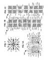
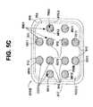
- FIG. 5Ashows a stacked multiple, circuit network including groups of pathways according to an aspect of the present invention
- FIG. 5Bshows a stacked shield according to an aspect of the present invention
- FIG. 5Cshows a relative plan view of a stacked multiple, non-shared circuit network having VlAs including groups of pathways according to an aspect of the present invention
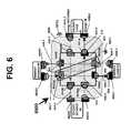
- FIG. 6shows a relative plan view of circuit arrangement variant according to an aspect of the present invention.
- FIG. 7shows a relative plan view of circuit arrangement variant according to an aspect of the present invention.
- an “energy pathway” or “pathway”may be at least one, or a number, of conductive materials, each one operable for sustained propagation of energy. Pathways may be conductive, thereby better propagating various electrical energies as compared to non-conductive or semi-conductive materials directly or indirectly coupled to, or adjacent to, the pathways.
- An energy pathwaymay facilitate propagation of a first energy by allowing for various energy conditioning functions, such as conditioning functions arising due to any one or a number of aspects, such as, but not limited to, the shielding, the orientation and/or the positioning of the energy pathways within the energy pathway arrangement, which various arrangements having an orientation and/or positioning thereby allow for interaction of the first energy with propagating energies that are complementary to at least the first energy.
- An energy pathwaymay include an energy pathway portion, an entire energy pathway, a conductor, an energy conductor, an electrode, at least one process-created conductor, and/or a shield.
- a plurality of energy pathwaysmay include a plurality of each device or element discussed hereinabove with respect to energy pathway.
- a conductormay include, for example, an individual conductive material portion, a conductive plane, a conductive pathway, a pathway, an electrical wire, a via, an aperture, a conductive portion such as a resistive lead, a conductive material portion, or an electrical plate, such as plates separated by at least one medium 801 , for example.
- a shieldmay include a shielding electrode, a shielding pathway portion, a shielded pathway, a shielded conductor, a shielded energy conductor, a shielded electrode, and/or at least one process-created shielded pathway portion.
- a plurality of shieldsmay include a plurality of the devices discussed hereinabove with respect to a shield.
- a pathwaymay be complementary positioned, or complementary orientated, with respect to a main-body 80 , 81 , having various pathway extensions, designated 79 ′′X′′, 812 ′′X′′, 811 ′′X′′and 99 ′′X′′.
- Main-bodies 80 , 81may be in three-dimensional physical relationships individually, in pairs, groups, and/or pluralities as to distance, orientation, position, superposition, non-superposition, alignment, partial alignment, lapping, non-lapping, and partial lapping.
- Superposed main-body pathway 80may, for example include a pairing of physically opposing and oppositely orientated main-body pathways 80 that are any one of, or any combination of, electrically null, electrically complementary, electrically differential, or electrically opposite.
- a pathway arrangementmay include at least a shield at least partially shielding at least one energy pathway, or a group of shields forming a shield structure that at least partially shielding, via a conductive shielding, at least a conductively isolated pairing of at least two energy pathways, such as vias, apertures or complementary paired pathways.
- An exemplary embodimentmay allow energy propagation on a conductively isolated pairing, such as complementary paired pathways, causing energy propagation on common shields, or at least one grouping of shields, serving an isolated circuit.
- This embodimentmay allow a low inductance pathway to form among at least a single pair of isolated and separate parallel pathways serving at least one separate and distinct isolated circuit system.
- An exemplary embodimentmay allow for the development of at least a low inductance pathway for utilization of energy propagating on at least one parallel pathway of at least two sets of isolated and separate parallel pathways and the development along at least one parallel pathway of at least one other low inductance pathway for utilization of energy propagating along at least one other separate and distinct isolated circuit system.
- An exemplary embodiment utilized as part of a circuit assemblymay have at least one pathway of relatively lower inductance, while other pathways may be electrically coupled to an energy source or an energy load.
- a pathway of a second plurality of pathwaysmay have a lower impedance operable for portions of energy to be taken away from either of the same at least one energy source or at least one energy load of the circuit assembly.
- This same pathway of low impedancemay not be electrically directly coupled to either the same at least one energy source or at least one energy load of the circuit assembly as the one pathway of lower inductance.
- a systemmay have both a pathway of least inductance and a pathway of least impedance which are not the same pathway.
- the pathway of least impedance and the pathway of least inductance for a circuit for energy conditioningmay be achieved independent of the physical size of the device. These aspects depend on a predetermined capacitance developed by a predetermined layers in the present invention.
- Arranging the pathwaysallows the resistance of the conductive material of the pathways to primarily determine the energy delivery, or relative efficiency or effect between at least one source of energy and one energy utilizing load of an integrated circuit, for example.
- the ESLmay be a negligible factor, rather than a primary factor for delivery outcome or decoupling void of debilitating inductances.
- the pathway arrangementupon placement into a circuit arrangement, may allow for energy propagation within or along certain energy pathways of the pathway arrangement, thereby allowing for the mutual interaction of opposite portions of pathway-sourced magnetic fields produced by the propagation of energy field currents emanating outwardly from each set of the complementary conductors.
- This mutual interactionmay be a mutual cancellation in embodiments wherein certain pathways may be partially or totally physically shielded from other complementary pathways, and may be placed within an influencing distance of those other complementary pathways.
- a substantial similarity in size and shape of the respective complementary pathwaysmay contribute to this mutual cancellation effect.
- the shielding operationsmay be predicated on a relative positioning of a mating of the paired pathways relative to the conductive electrostatic shielding.
- At least the complementary energy conditioning functions and electrostatic shielding dynamics discussed hereinmay operate on various energy propagating in various directions along various predetermined pathways, and may operate on circuits having dynamic operation utilizing the pathway arrangement.
- a sub-combination of electromagnetically/electrostatically actuated impedance statesmay develop along or within a pathway arrangement, or along or within a closely coupled external conductive portion conductively coupled to separate or multiple groupings of shields, to thereby form an energy conditioning circuit.
- These electromagnetically/electrostatically actuated impedance statesmay develop, for example, because of the energization of one paired set of pathways of one circuit portion, but not necessarily develop on another paired set of pathways from another circuit portion, for example.
- each shieldmay include a main-body 81 .
- Main-bodies 81may collectively and conductively couple to one another and at the same time may substantially immure and shield the main-body 80 of the energy pathways.
- the collective shielding main-body 81may only partially immure or shield the pathway main-body 80 s in at least one portion of the shielding.
- a balanced, symmetrical, pathway arrangementmay result from the symmetry of certain superposed shields, from complementary pathway sizing and shaping, and/or from reciprocal positioning and pairing of the complementary pathways.
- Manufacturable balanced or symmetrical physical arrangements of pathways, wherein dynamic energy propagation, interactions, pairings or match-ups of various dynamic quantities occur,may operate at less than a fundamental limit of accuracy of testing equipment. Thus, when portions of these complementary energy quantities interact simultaneously, the energy may be beyond the quantifiable range of the typical testing equipment.
- the extent to which the measurement may be obtainedmay employ increased controllability, and thereby the electrical characteristics and the effect on electrical characteristics may be controlled, such as by predetermining the desired measurability, behavior or enhancement to be provided, and by a correspondent arrangement of the elements, such as specifically by an arrangement of the elements to provide the desired measurability or effect.
- a desired electrical characteristicmay be predetermined for a desired enhancement by varying at least a portion of the complementary balance, size, shape, and symmetry of at least one pathway pairing, as set forth herein below and as illustrated in FIGS. 1A , 1 B, 1 C, 5 A and 5 B, for example.
- the extent of energy interactions, mutual energy propagation timings and interferencesmay be controlled by tolerances within the pathway arrangement.
- a manufacturing process, or computer tolerance control, such as semiconductor process control,may control these tolerances, for example.
- the pathways of an embodimentmay be formed using manufacturing processes, such as passive device processes, apparent to those skilled in the art. Mutual energy propagation measurements may thereby be cancelled or suppressed by the formation, and process of formation, of the pathway arrangement.
- a pathway arrangementmay, as set forth hereinabove, include a sequentially positioned grouping of pathways in an amalgamated electronic structure having balanced groupings of pathways.
- the balanced groupingmay include a predetermined pathway architecture having a stacked hierarchy of pathways that are symmetrical and complementary in number, and that are positioned complementary to one another, thereby forming pairs, each of which pair is substantially equidistant from each side of a centrally positioned shield, wherein each shield may provide a symmetrical balancing point for both each pair pathway and the overall pathway hierarchy as depicted in FIGS. 1A to 4I , for example.
- predetermined identically sized, shaped and complementary positioned pathwaysmay be present on either side of a centrally positioned shield for each separate circuit portion.
- a total circuitmay have its complementary portions symmetrically divided into a complementary physical format including a reverse-mirror image positioning of paired shielded, complementary sized and shaped pathways, sandwiching at least one interposing shield.
- each pathwaymay be, for example, a first interconnect substrate wrapping around, or holding, an integrated circuit wafer, a deposit, an etching, or a resultant of a doping process
- the shieldmay be, for example, a pathway substrate, an energy conditioning embodiment or energy conditioning substrate, a deposit, an etching, a resultant of a doping process, and may have, for example, resistive properties.
- Additional elementsmay be utilized, including conductive and nonconductive elements, between the various pathways. These additional elements may take the form of ferromagnetic materials or ferromagnetic-like dielectric layers, and/or inductive-ferrite dielectric derivative materials. Additional pathway structural elements may be utilized, including conductive and nonconductive multiple pathways of different conductive material compositions, conductive magnetic field-influencing material hybrids and conductive polymer sheets, various processed conductive and nonconductive laminates, straight conductive deposits, multiple shielding pathways utilizing various types of magnetic material shields and selective shielding, and conductively doped and conductively deposited on the materials and termination solder, for example, in addition to various combinations of material and structural elements, to provide a host of energy conditioning options.
- Non-conductor materialsmay also provide structural support of the various pathways, and these non-conductor materials may aid the overall energized circuit in maintaining the simultaneous, constant and uninterrupted energy propagation moving along the pathways.
- Dielectric materialsmay include one or more layers of material elements compatible with available processing technology. These dielectric materials may be a semiconductor material such as silicon, germanium, gallium arsenide, or a semi-insulating and insulating material such as, but not limited to any K, high K and low K dielectrics.
- Pathway and conductor materialsmay be selected from a group consisting of Ag, Ag/Pd, Cu, Ni, Pt, Au, Pd and other such conductive materials and metals. Combinations of these metal materials are suitable for the purposes discussed herein, and may include appropriate metal oxides, such as ruthenium oxide, which, depending on the exigencies of a particular application, may be diluted with a suitable metal. Other pathways may be formed of a substantially non-resistive conductive material.
- Any substances and processes that may create pathways from conductive, non-conductive, semi-conductive material, and/or Mylar films printed circuit board materials, or any substances or processes that may create conductive areas such as doped polysilicons, sintered polycrystallines, metals, polysilicon silicates, or polysilicon silicidemay be used within or with the pathway arrangement.
- An exemplary embodiment of the present inventionmay utilize an internal shield structural architecture to insure energy balancing configurations within the various arrangements, rather than a specific external circuit balance.
- This balancing configurationis dependent upon the relative positioning of all the shields in relationship to the shared and centrally positioned shield, and the actual paired shields positioned in specific quantities, to simultaneously provide shielding for the electrically opposing shielded paired pathways utilized by propagating energy.
- This interposition of the central and shared shieldsmay create a voltage divider that divides various circuit voltages in half and that provides, to each of the oppositely paired shielded conductors, one half of the voltage energy normally expected.
- the energized circuitry, including shielded conductorsmay be balanced electrically or in a charge-opposing manner and with respect to a centrally positioned shield, to a common and shared pathway, or to each respective, isolated circuit system
- Each common circuit member of an isolated circuit systemmay be attached or coupled to a common area or common pathway, thereby providing an external common zero voltage.
- the embodimentmay have multiple sets of shields electrically or physically located between at least one of the various electrically or charge opposing, shielded pairs or grouped complementary pairs of pathways in an interposed shielding relationship, supported with additional outer sandwiching shields, designated herein as-IM that are additionally coupled and, in part, form the shielding structure.
- An exemplary embodimentmay also be placed into one or more energy circuits that utilize different energy sources and that may supply one or more separate and distinct energy-utilizing loads.
- each separate and distinct circuitis utilizing the multiple commonly shared universal shield structure and circuit reference image, or node.
- energy-conditioning functionsmay maintain an apparent balanced energy voltage reference and energy supply for each respective energy-utilizing load within a circuit.
- This energized arrangementmay allow for specific energy propagation utilizing a single, or multiple, isolated pathway arrangement, and may not require balancing on a single, centralized shield.
- a shieldmay be physically and electrically located between one or multiple energy sources and one or multiple energy utilizing loads, depending upon the number of separate and isolated pathways.
- shielding relative, centralized pathwaysmay be in both co-planar and stacked variants of exemplary embodiment.
- the internally positioned paired shieldsWhen the internally positioned paired shielded pathways are subsequently attached, or conductively coupled, to externally manufactured pathways, the internally positioned paired shields may be substantially enveloped within the cage-like shield structure, thereby minimizing internally generated energy strays and parasitics that may normally escape or couple to an adjacent shielded pathway.
- These shielding modesutilize propagating energy to the various pathways and may be separate of the electrostatic shield effect created by the energization of the shield structure.
- the propagating energy propagating in a complementary mannerprovides energy fields of mutually opposed, mutually cancelled fields as a result of the close proximity of opposite propagation.
- the complementary and paired pathwaysmay provide an internally balanced opposing resistance load function.
- a devicemay mimic the functionality of at least one electrostatically shielded transformer.
- Transformersmay be widely used to provide common mode isolation dependent upon a differential mode transfer across the inputs in order to magnetically link the primary windings to the secondary windings to transfer energy. As a result, common mode voltage across the primary winding is rejected.
- One flaw inherent in the manufacturing of transformersis the propagating energy source capacitance between the primary and secondary windings. As the frequency of the circuit increases, so does capacitive coupling, until circuit isolation may be compromised. If enough parasitic capacitance exists, high frequency RF energy may pass through the transformer and cause an upset in the circuits on the other side of the isolation gap subjected to the transient event.
- a shieldmay be provided between the primary and secondary windings by coupling to a common pathway reference source designed to prevent capacitive coupling between the multiple sets of windings.
- a device according to an aspect of the present inventionimproves upon, and reduces the need for, transformers in circuits.
- the devicemay use a physical and relative, common pathway shield to suppress parasitics and also may use relative positioning of common pathway shields, a complementary paired pathway layering, the various couplings of the pathway layering, and an external conductive coupling to a conductive area per isolated circuit system, in combination with the various external circuitry, to effectively function as a transformer.
- the electrostatically shielded, transformer function of the device discussed hereinmay be effective for transient suppression and protection, and may simultaneously operate as a combined differential mode and common mode filter.
- Each set of relative shields and relative conductorsmay be conductively coupled to at least the same external pathway to provide a transformer functionality for example.
- Propagated electromagnetic interferencemay be the product of both electric and magnetic fields.
- a device according to an aspect of the present inventionmay be capable of conditioning energy that uses DC, AC, and AC/DC hybrid-type propagation, including conditioning energy in systems that may contain different types of energy propagation formats and in systems that may contain more than one circuit propagation characteristic.
- perimeter conductive coupling material for coupling or connecting, by conductive joining, of external portions of a typical embodiment into an assemblymay be accomplished by conductive or non-conductive attachments to various types of angled, parallel or perpendicular, as those terms apply relative to at least another pathway, conductors known as apertures or blind or non-blind VlAs, passing through, or almost through, portions respectively of an exemplary embodiment.
- Couplings to at least one or more load (s), such as a portion of an integrated circuit, for one aspect of the inventionmay involve a selective coupling, or not, to these various types of conductors, such as apertures and VIAs.
- Fabricating a pathwaymay include forming one or more plated through hole (PTH) via (s) through one or more levels of a pathway.
- Electronic packagescommonly include multiple interconnect levels.
- the inventionmay include layering of patterned conductive material on one interconnect level that may be electrically insulated from patterned conductive material on another interconnect level, such as by dielectric material layers.
- Connections or couplings between the conductive material at the various interconnect levelsmay be made by forming openings, referred to herein as vias or apertures, in the insulating portions or layers, that in turn can provide an electrically conductive structure such that the patterned or shaped conductive material portions or pathways from different levels are brought into electrical contact with each other. These structures can extend through one or more of the interconnect levels.
- Use of conductive, non-conductive or conductively-filled apertures and VlAsallows propagating energy to transverse an exemplary embodiment as if utilizing a by-pass or feed-through pathway configuration of an embodiment.
- An embodimentmay serve as a support, a system or a subsystem platform that may contain both or either active and passive components layered to provide the benefits described for conditioning propagated energy between at least one source and at least one load.
- An aspect of the present inventionmay provide a conductive architecture or structure suitable for inclusion in a packaging or an integrated circuit package having other elements.
- Typical capacitive balances found between at least one shielding pathwaymay be found when measuring opposite sides of the shared shield structure per isolated circuit, and may be maintained at measured capacitive levels within this isolated circuit portion, even with the use of common non-specialized dielectrics or pathway conductive materials.
- complementary capacitive balancing, or tolerance balancing characteristics, of this type of electrical circuit due to element positioning, size, separations and attachment positioningallow an exemplary embodiment having an isolated circuit system manufactured at 3% capacitive tolerance, internally, to pass to a conductively coupled and energized isolated circuit system a maintained and correlated 3% capacitive tolerance between electrically opposing and paired complementary pathways of each respective isolated circuit system, with respect to the dividing shield structures placed into the isolated circuit system.
- An exemplary embodimentmay allow utilization of relatively inexpensive dielectrics, conductive materials and various other material elements in a wide variety of ways. Due to the nature of the architecture, the physical and electrical dividing structure created may allow the voltage dividing and balancing among the grouped, adjacent elements, and may allow for the minimization of the effect of material hysteresis and piezoelectric phenomenon to such a degree that propagating energy normally disrupted or lost to these effects may be essentially retained in the form of active component switching response time, as well as instantaneous ability to appear to the various energy-utilizing loads as an apparent open energy flow simultaneously on both electrical sides of a pathway connecting or coupling from an energy source to a respective load, and from the load back to the source.
- a structured layermay be shaped, buried within, enveloped by, or inserted into various electrical systems and sub-systems to perform line conditioning or decoupling, for example, and to aid in or to allow for a modifying of an electrical transmission of energy to a desired or predetermined electrical characteristic.
- Expensive, specialized, dielectric materialsthat attempt to maintain specific or narrow energy conditioning or voltage balancing may no longer be needed for bypass, feed through, or energy decoupling operations for a circuit.
- a devicemay, as set forth hereinabove, be placed between each isolated circuit and a paired plurality of pathways or differential pathways.
- This exemplary devicemay operate effectively across a broad frequency range, as compared to a single discrete capacitor or inductor component, and may continue to perform effectively within an isolated circuit system operating beyond, for example, a GHz.
- the exemplary devicemay perform shielding functions in this broad frequency range.
- a physical shielding of paired, electrically opposing and adjacent complementary pathwaysmay result from the size of the common pathways in relationship to the size of the complementary pathways, and from the energized, electrostatic suppression or minimization of parasitics originating from the sandwiched complementary conductors and preventing external parasitics.
- the positioning of the shielding, relative to shielding that is more conductivemay be used to protect against inductive energy and “H-Field” coupling. This technique is known as mutual inductive cancellation.
- Parasitic couplingis known as electric field coupling.
- the shielding function discussed hereinaboveprovides primary shielding of the various shielded pathways electrostatically against electric field parasitics.
- Parasitic coupling involving the passage of interfering propagating energy because of mutual or stray parasitic energy originating from the complementary conductor pathwaysmay be thereby suppressed.
- a device according to an aspect of the present inventionmay, for example, block capacitive coupling by enveloping oppositely phased conductors in the universal shield architecture with stacked conductive hierarchical progression, thereby providing an electrostatic or Faraday shield effect with respect to the pathway positioning as to the respective layering and position, both vertically and horizontally, of the pathways.
- the shielding pathway architecturemay be used to suppress and prevent internal and external parasitic coupling between potentially noisy conductors and victim conductors, such as by an imposition of a number of common pathway layers that are larger than the smaller paired complementary pathways, but that are positioned between each of the complementary pathway conductor pairs to suppress and to contain the stray parasitics.
- shieldingpositioning of the shielding, relative to shielding that is more conductive, may be used against inductive energy and “H-Field” coupling.
- This cancellationis accomplished by physically shielding energy, while simultaneously using a complementary and paired pathway positioned to allow for the insetting of the contained and paired complementary pathways within an area size correspondent to the shield size.
- a device according to an aspect of the present inventionis adapted to use shields separately as internal shields or groupings, thereby substantially isolating and sandwiching pairs of electrically opposing complementary pathways, and thereby providing a physically tight or minimized energy and circuit loop propagation path between each shield and the active load.
- shields and non-shieldsmay allow energy along shields even if a direct electrical isolation exists because of 801 material type or the spacing.
- Flux cancellation of propagating energy along paired and electrically opposing or differential pathwaysmay result from spacing of pathways apart by a very small distance for oppositely phased electrically complementary operations, thereby resulting in a simultaneous stray parasitic suppression and containment function attributable to tandem shielding, and thereby enhancing energy conditioning.
- additional shielding energy currentsmay be distributed around component shielding architectures.
- a plurality of shields as described hereinabovemay be electrically coupled as either an isolated circuit's reference node, or chassis ground, and may be relied on as a commonly used reference pathway for a circuit.
- the various groups of internally paired, complementary pathwaysmay include propagating energy originating from one or more energy sources propagating along external pathways coupled to the circuit by a conductive material. Energy may thus enter the device, undergo conditioning, and continue to each respective load.
- the shielding structuremay allow for a portion of a shield to operate as the pathway of low impedance for dumping and suppressing, as well as at least partially blocking return of unwanted electromagnetic interference noise and energy into each of the respective energized circuits.
- internally located shieldsmay be conductively coupled to a conductive area, thereby adaptively utilizing shielding structure for low impedance dumping and suppressing and at least partially blocking return blocking of unwanted electromagnetic interference noise and energy.
- another set of internally located shieldsmay be conductively coupled to a second conductive area, thereby utilizing shields for low impedance dumping, suppressing and at least partially blocking the return of unwanted electromagnetic interference noise and energy.
- the conductive areasmay be electrically or conductively isolated from one another.
- Simultaneous suppression of energy parasiticsmay be attributed to the enveloping shielding pathway structure, in combination with the cancellation of mutually opposing energy fields, and may be further attributed to the electrically opposing shielded pathways and propagating energy along the various circuit pathways interacting within the various isolated circuits to undergo a conditioning effect taking place upon the propagating energy.
- This conditioningmay include minimizing effects of H-field energy and E-field energy through simultaneous functions, such as through isolated circuits that contain and maintain a defined electrical area adjacent to dynamic simultaneous low and high impedance pathways of shielding in which various paired pathways have their respective potentials respectively switching as a result of a given potential located on a shielding and used instantaneously and oppositely by these pairings with respect to the utilization by energy found along paired routings of the low and high impedance shields.
- the various distance relationships created by the positional overlapping of energy routings within the isolated circuitscombine with the various dynamic energy movements to enhance and cancel the various degrees of detrimental energy disruptions normally occurring within active components or loads.
- the efficient energy conditioning functions occurring within the passive layering architectureallow for development of a dynamic “0” impedance energy “black hole”, or energy drain, along a third pathway coupled common to both complementary pathways and adapted to allow energy to be contained and dissipated upon the shielding, within the various isolated circuits and attached or conductively coupled circuits.
- electrically opposing energiesmay be separated by dielectric material and/or by an interposition shield structure, thereby allowing dynamic and close distance relationship within a specific circuit architecture, and thereby taking advantage of propagating energy and relative distances to allow for exploitation of mutual enhancing cancellation phenomenon and an electrostatic suppression phenomenon to exponentially allow layered conductive and dielectric elements to become highly efficient in energy handling ability.
- a devicemay utilize a single low impedance pathway or a common low impedance pathway as a voltage reference, while utilizing a circuit maintained and balanced within a relative electrical reference point, thereby maintaining minimal parasitic contribution and disruptive energy parasitics in the isolated circuit system.
- the various attachment schemes described hereinmay allow a “0” voltage reference, as discussed hereinabove, to develop with respect to each pair or plurality of paired complementary conductors located on opposite sides of the shared central shield, thereby allowing a voltage to be maintained and balanced, even with multiple Simultaneous Switching Operations states among transistor gates located within an active integrated circuit, with minimal disruptive energy parasitics in an isolated circuit.
- Shieldsmay be joined using principals of a cage-like conductive shield structure to create one or more shieldings.
- the conductive coupling of shields together with a larger external conductive areamay suppress radiated electromagnetic emissions and as a larger area provides a greater conductive area in which dissipation of voltages and surges may occur.
- One or more of a plurality of conductive or dielectric materials having different electrical characteristicsmay be maintained between shields.
- a specific complementary pathwaymay include a plurality of commonly conductive structures performing differentially phased conditioning with respect to a “mate”, or paired, plurality of oppositely phased or charged structures forming half of the total sum of manufactured complementary pathways, wherein one half of the complementary pathways forms a first plurality of pathways, and wherein the second half forms a second plurality of pathways.
- the sum of the complementary pathways of the first and the second plurality of pathwaysmay be evenly separated electrically, with an equal number of pathways used simultaneously, but with half the total sum of the individual complementary pathways operating from, for example, a range of 1 degree to approximately 180 degrees electrically out of phase from the oppositely positioned groupings.
- Small amounts of dielectric materialsuch as microns or less, may be used as the conductive material separation between pathways, in addition to the interposing shield, which dielectric may not directly physically or conductively couple to any of the complementarily operating shielded pathways.
- An external ground areamay couple or conductively connect as an alternative common pathway. Additional numbers of paired external pathways may be attached to lower the circuit impedance. This low impedance phenomenon may occur using alternative or auxiliary circuit return pathways.
- a shield architecturemay allow shields to be joined together, thereby facilitating energy propagation along a newly developed low impedance pathway, and thereby allowing unwanted electromagnetic interference or noise to move to this created low impedance pathway.
- FIG. 1A through FIG. 5Bwhich generally show various common principals of both common and individual variants of an exemplary embodiment configured in a co-planar variant ( FIGS. 1A-4I ) and a stacked variant ( FIGS. 5A and 5B ).
- FIG. 1Athere are shown relative locations of the various pathway extensions disclosed according to an aspect of the present invention.
- a portion of a relative balanced and complementary-symmetrical arrangement utilizing a center shielding pathway designated 8 “XX”-“X”Mis adapted in the arrangement as the fulcrum of balanced conductive portions in a co-planar variant.
- At least a first half of the second pluralityis arranged electrically isolated from a second half of the second plurality, wherein at least two pathways of the second plurality are electrically isolated from the pathways of first plurality.
- the pathway arrangementmay also include a material having properties, such as dielectric, ferromagnetic, or varistor for example, spacing apart pathways of the pathway arrangement.
- the pathways of the first half of the second pluralityare electrically coupled to one another, and the pathways of the second half of the second plurality are electrically coupled to one another.
- a total number of pathways of the first half of the second pluralitymay be an odd number greater than one, and a total number of pathways of a second half of the second plurality may also be an odd number greater than one.
- the pathways of the first half of the second pluralityare positioned in a first superposed alignment, while the pathways of the second half of the second plurality are positioned in a second superposed alignment, with the first and second superposed alignments in a mutual superposed alignment herein defined as a co-planar arrangement.
- the pathways of the first half of the second pluralitymay be positioned in a first superposed alignment, and the pathways of the second half of the second plurality may be positioned in a second superposed alignment, with the first and second superposed alignments in arrangement one atop the other.
- at least four pathwaysare electrically isolated.
- An illustrative embodiment of the present inventionmay include at least three pluralities of pathways, including a first plurality of pathways and a second plurality of pathways.
- the first and second pluralities of pathwaysmay include pathway members of the first plurality having an equal and opposite pathway member found in the second plurality of pathways.
- Members of the first and second pluralities of pathwaysmay be substantially the same size and shape, and may be positioned complementary, and may also operate in an electrically complementary manner.
- the pairings of the first and second pluralities of pathwaysmay result in identical numbers of members of the first and second pluralities of pathways.
- An exemplary embodimentmay provide at least a first and a second shield allowing for development of individual isolated low circuit impedance pathways.
- the shieldsmay be accomplished by a third plurality of pathways and a fourth plurality of pathways.
- Each shielding pluralitymay include shields of equal size and shape.
- Each of the third and fourth plurality of pathwaysmay be conductively coupled. Conductive coupling may be accomplished by a variety of methods and materials known to those possessing an ordinary skill in the pertinent arts.
- the third and fourth pluralitiesmay be coupled to a common pathway to develop a low circuit impedance pathway for energy propagation for conditioning of the circuit energy.
- Pathwaysmay additionally be arranged in a bypass arrangement, such that when placed face to face, main-body pathways 80 may be aligned superposed, with the exception of any pathway extensions such as 812 NNE, 811 NNE, 812 SSW and 811 SSW of the lower sub-circuit portion, for example, shown as mirror images depicted in FIG. 5A and FIG. 5B , for example.
- individual pathway membersmay be of substantially the same size and shape and may be conductively coupled. However, individual pathway members of one plurality may not be conductively coupled to members of a different plurality of pathways.
- members of one pluralitymay be connected to members of a different plurality, such as wherein a first plurality of shields and a second plurality of shields are externally coupled to the same conductor.
- Common elementsmay include energy flow in accordance with conceptual energy indicators 600 , 601 , 602 , 603 depicting the dynamic energy movements in co-planar shielded by-pass pathways, such as those shown in FIG. 1A-1C .
- An embodimentmay provide for at least multiple shields for development of multiple isolated low circuit impedance pathways for multiple circuits.
- pathwaysmay be shielded by the relative, common pathways, and may include a main-body pathway 80 with at least one pathway extension 812 “X”.
- the shields showninclude a main-body shield pathway 81 with at least one pathway extension designated 99 “X”/ 79 “X”.
- the shieldsmay sandwich and envelope the main-body 799 , including a conductive inner pathway formed of conductive materials from the family of noble or base metals traditionally used in co-fired electronic components or conductive material, such as Ag, Ag/Pd, Cu, Ni, Pt, Au, Pd, or combination materials such as metal oxide and glass frit.
- a capacitance and a resistance valuemay be achieved in one family of pathways, as described hereinabove, such as by use of ruthenium oxide as the resistive material and Ag/Pd as the conductive material. Further, variations in pathway geometry may yield different resistance and capacitance values. Variations may be achieved by altering the materials from which the pathways are made. For example, a conductive metal, such as silver, may be selectively added to the metal oxide/glass frit material to lower the resistance of the material.
- a plurality of pathways, 865 - 1 and 865 - 2are shown positioned co-planar and spaced apart on a same portion of material 801 .
- Each pathway of the co-planar pathways 865 - 1 and 865 - 2may be formed of conductive material 799 , or a hybrid of conductive material and another material, herein designated as 799 “x”.
- Each co planar pathway 865 - 1 and 865 - 2may also be formed as a bypass pathway, wherein each pathway includes a main-body pathway 80 having a corresponding main-body edge and perimeter, 803 A and 803 B, respectively and at least one pathway contiguous extension 812 “X”.
- Each co-planar pathway 865 - 1 and 865 - 2may include at least one pathway contiguous extension 812 SSW and 811 SSW with a portion of the main-body edge 803 A and 803 B extending therefrom.
- Extension 812 “X”is a portion of the pathway material formed in conjunction with a main-body pathway 80 from which it extends.
- Main-body pathway 80an 812 “X” may be found as an extension of material 799 or 799 “x” extending beyond an accepted average perimeter edge 803 “X”.
- Extensions 812 “X” and 79 “X”may be found respectively positioned as a contiguous portion of the pathway from which it is formed.
- Each main-body pathwaymay have edge 803 A, 803 B positioned relative and spaced apart a distance 814 F from the embodiment edge 817 .
- Embodiment edge 817may include a material 801 .
- Co-planar main-body pathway's edge 803 “x”may be positioned and spaced apart a distance 814 J.
- Pathway extensions 812 SSW and 811 SSWmay conductively couple a respective pathway main-body 80 to an outer pathway 890 SSW and 891 SSW, which may be positioned at edge 817 .
- the co-planar arranged, main-body pathway 80may be positioned “sandwiched ” between the area of registered coverage of two layering of co-planar, main-body pathway 81 s.
- the edges of the plurality of co-planar shieldsmay be represented by dotted lines 805 A and 805 B.
- Main-body pathways 81 of each of the plurality of shieldsare larger than a sandwiching main-body pathway 80 of any corresponding sandwiched pathway. This may create an inset area 806 relative to the positions of the shields and remaining pathways.
- the size of main-bodies 80 and 81may be substantially similar, and thus the insetting positioning relationships may be minimal in certain embodiments. Increased parasitic suppression may be obtained by insetting pathways, including a main-body 80 , to be shielded by larger pathway main-body 81 s.
- an inset of a main-body 80 of pathways 865 - 1 insetmay be separated a distance of 1 to 20+ times the spacing provided by the thickness of the material 801 separating pathway 865 - 1 and adjacent center co-planar pathway 800 - 1 -IM, as illustrated in FIG. 1B .
- Plurality of co-planar shield edges 805 A and 805 Bmay be positioned and spaced apart a distance 814 K, and may be a distance 814 relative to edges 805 A and 805 B and the edge 817 .
- Other distances 814 J relative from either edges 803 A and 803 Bmay be provided.
- Each co- planar shieldmay include a plurality of contiguous pathway extension portions, such as, for example, portions 79 NNE, 79 SSE, 99 NNE and 99 SSE, extending from the plurality of co- planar shield edges 805 A and 805 B.
- Plurality of co-planar shieldsmay include a plurality of outer pathway material 901 NNE, 901 SSE, 902 NNE and 902 SSE positioned at the edge 817 .
- Conceptual energy indicators 602represent the various dynamic energy movements within the co-planar pathways 865 - 1 and 865 - 2 . Unwanted energy may be transferred to the co-planar shields in accordance with the provision by the shields providing for a low impedance pathway, which shields may additionally be electrically coupled to another pathway or conductive area.
- first, second, and third pluralitiesmay be stacked to form an embodiment 3199 , 3200 , 3201 .
- the third plurality of co-planar pathwaysmay provide shielding.
- Main-bodies 81 of the plurality of co-planer shields 825 - 1 -IM, 825 - 2 -IM; 815 - 1 , 815 - 2 ; 800 - 1 -IM, 800 - 2 -IM; 810 - 1 , 810 - 2 ; and 820 - 1 -IM, 820 - 2 -IMmay be substantially similar in size and shape, and may be spaced apart in co-planar locations on different layers of material 801 .
- the first plurality of co-planar pathways 865 - 1 and 865 - 2may have at least the corresponding, opposing, and complementary second plurality of co-planar pathways 855 - 1 and 855 - 2 .
- These first and second pluralities of co-planar pathwayswhen oriented face to face, may have main-body pathways 80 s co-registered and aligned except for the various contiguous pathway extensions 812 “X”, 811 “X”.
- a pair of outer co-planar pathways 820 - 1 -IM, 825 - 1 -IMmay serve as pathway shields, thereby improving the shielding effectiveness of the other conductively coupled pluralities of pathways with a main-body 81 s.
- extensions 79 NNE, 79 SSE, of shields 825 - 1 -IM, 815 - 1 , 800 - 1 -IM, 810 - 1 , and 820 - 1 -IM and extensions 99 NNE, 99 SSE of the shields 825 - 2 -IM, 815 - 2 , 800 - 2 -IM, 810 - 2 , and 820 - 2 -IMmay be varied.
- extensions 79 NNE and 99 NNEmay be arranged spaced apart, diagonally from extensions 79 SSE and 99 SSE and on opposite sides of shield main- body 81 .
- FIG. 1Bfor example, extensions 79 NNE and 99 NNE may be arranged spaced apart, diagonally from extensions 79 SSE and 99 SSE and on opposite sides of shield main- body 81 .
- extensions 79 NNE and 99 NNEmay be arranged spaced apart in line with extensions 79 SSE and 99 SSE on opposite sides of shield main-body 81 .
- extensions 812 NNE and 811 NNEmay be arranged spaced apart, extending toward the same edge 812 of layer of material 801
- extensions 812 SSW and 811 SSWmay be arranged spaced apart, each extending toward the opposite edge 812 of layer of material 801 .
- pathways 865 - 1 and 865 - 2may be mirror images, as discussed hereinabove. Comparably to FIG.
- extensions 812 NNE and 811 NNEmay be arranged spaced apart, extending toward opposite edges 817 of layer of material 801 .
- Extensions 812 SSW and 811 SSWmay be arranged spaced apart, extending toward the opposite edge of layer of material 801 , such that extensions 812 NNE and 811 SSW extend toward opposite edges 812 “X” of the respective layer of material 801 .
- FIG. 2Aillustrates a schematic plan view of an embodiment of FIG. 2B according to an aspect of the present invention.
- FIG. 2Bdepicts a pathway arrangement including a layout of a first, a second, a third, a fourth, a fifth, a sixth, a seventh, a eighth, a ninth and a tenth pathway, wherein at least the third and the fourth pathway, for example, may be co-planar and arranged spaced apart from each other.
- FIG. 2Bdepicts a pathway arrangement including a layout of a first, a second, a third, a fourth, a fifth, a sixth, a seventh, a eighth, a ninth and a tenth pathway, wherein at least the third and the fourth pathway, for example, may be co-planar and arranged spaced apart from each other.
- FIG. 2Billustrates the first and the second pathway arranged below the third and the fourth pathway, and the fifth and the sixth pathway arranged above the third and the fourth pathway, and the seventh and the eighth pathway arranged above the fifth and the sixth pathway, and the ninth and the tenth pathway, arranged above the seventh and the eighth pathway.
- These pathwayshave various respective internal contiguous pathway extensions 812 “X”, 811 “X”, 79 “X” and 99 “X”, and may be discrete components having the same minimal numbers of layering.
- Internal contiguous pathway extensions 812 “X”, 811 “X”, 79 “X” and 99 “X”, and conductively coupled external pathways 890 “X”, 891 “X” 802 “X” and 902 “X”,may be coupled to the inner pathway of the plurality of co-planar pathways of the main-body pathway 80 and 81 .
- FIG. 3Athere is shown a schematic plan view of an embodiment of FIG. 3B , wherein outer pathways may be selectively conductively coupled in at least two isolated circuit portions.
- FIG. 3Bdepicts an pathway arrangement including a minimal layout of a first, a second, a third, a fourth, a fifth, a sixth, a seventh, a eighth, a ninth and a tenth pathway, wherein at least the third and the fourth pathway, for example, are co- planar and arranged spaced apart from each other.
- 3Bmay have the first and the second pathway arranged below the third and the fourth pathway, and the fifth and the sixth pathway arranged above the third and the fourth pathway, and the seventh and the eighth pathway arranged above the fifth and the sixth pathway, and the ninth and the tenth pathway arranged above the seventh and the eighth pathway.
- These pathwayshave various respective internal contiguous pathway extensions 812 “X”, 811 “X”, 79 “X” and 99 “X”, and may be discrete components having the same minimal number of layering.
- FIG. 3Ca plan view of a shield according to an aspect of the present invention is illustrated.
- the embodiment depicted in FIG. 3Cincludes at least one additional pathway, as compared to the device of FIG. 3B .
- This additional pathway 1100 -IM“X”may be one of at least a plurality of shields in the stack of pathways, which shields may span across the two circuit portions.
- Pathway 1100 -IM“X”may be one of at least two outer sandwiching shields in the stack of pathways. Shields may span across the two circuits by adding a centrally arranged 1100 -IM“X” pathway electrically coupled to the outer 1100 -IM“X” shields.
- Pathways 1100 -IM“X”may have at least one extension, and are illustrated with two extensions 1099 E and 1099 W, and may allow for sandwiching shields for all of the pathways within the present invention. At least three shields may be coupled together and may include a centering shield dividing an energy load or energy source of an isolated circuit or dividing two isolated circuits.
- a shield 00 GSmay be electrically isolated from other shields and may be arranged to effect an energy propagation of an isolated circuit.
- An isolated circuitmay be sandwiched by a shield.
- a shieldmay be electrically coupled to a conductive area that is isolated from any other conductive areas thereby effecting an energy propagation.
- FIGS. 4A-4Idepict assembled components of various embodiments according to aspects of the present invention.
- the arrangements of FIG. 4A to FIG. 4Imay include minimal layouts of a first, a second, a third, a fourth, a fifth, a sixth, a seventh, a eighth, a ninth and a tenth pathway, wherein at least the third and the fourth pathway, for example, are co-planar and arranged spaced apart from each other.
- the first and the second pathwaymay be arranged below the third and the fourth pathway, and the fifth and the sixth pathway may be arranged above the third and the fourth pathway, and the seventh and the eighth pathway may be arranged above the fifth and the sixth pathway, and the ninth and the tenth pathway may be arranged above the seventh and the eighth pathway.
- These pathwayshave various respective internal contiguous pathway extensions 812 “X”, 811 “X”, 79 “X” and 99 “X”, and may be an assembled final discrete component, for example.
- FIG. 5Athere is shown a stacking of multiple, non-shared circuits including groups of pathways according to an aspect of the present invention. Included in FIG. 5A is a marker 1000 showing a continuation of the stacking arrangement to the next column of FIG. 5A .
- Conceptual energy indicators 600 , 601 , 602 , 603indicate energy flow.
- Material 799may be deposited on material 801 for component 6900 shields designated 815 - 1 , 800 - 1 -IM, 810 - 1 , 815 - 2 , 800 - 2 -IM, and 810 - 2 .
- Shields 810 -A and 810 -Bare separated shields of at least part of an isolated circuit system.
- Shields 815 -A and 815 -Bare separated shields of at least part of an isolated circuit system.
- Shields 800 -A and 800 -Bare separated shields of at least part of an isolated circuit system.
- Shields 835 -A and 835 -Bare separated shields of at least part of an isolated circuit system.
- Conductors 855 - 1 and 855 - 2are separated and shielded pathways in bypass configuration.
- Conductors 865 - 1 and 865 - 2are separated and shielded pathways in bypass configuration.
- a pathway arrangementis depicted including at least six orientations of pathways of two types of pathways, wherein each orientation of the pathways of the at least six orientations of pathways provides conductive isolation from the remaining orientations of pathways.
- FIG. 5Bthere is shown a stacked shield structure according to an aspect of the present invention.
- FIG. 5Bdepicts an embodiment similar to that of FIG. 5A , wherein two sets of 855 “X” and 865 “X” pathways are omitted for purposes of clarity, and wherein the shields of FIG. 5A are oriented in flip-flop for each relative set of 855 “X” and 865 “X” pathways.
- the 79 “X” pathway extensionsmay be rotated 90 degrees relative to the various pathway extensions 811 “x” and 812 “X”.
- a dynamic result of this configurationmay be enhanced by nulling the extensions of the two sets of 855 “X” and 865 “X” pathways of the two isolated circuits, and by relatively positioning the shield of each isolated circuit pairing 855 A and 865 A approximately 90 degrees null to the various pathway extensions of 855 B and 865 B.
- FIG. 5Bthere is shown a stacked shield structure according to an aspect of the present invention.
- FIG. 5Bdepicts an embodiment similar to that of FIG. 5A , wherein two sets of 855 “X” and 865 “X” pathways are omitted for purposes of clarity, and wherein the shields of FIG. 5A are oriented in flip-flop for each relative set of 855 “X” and 865 “X” pathways.
- the 79 “X” pathway extensionsmay be rotated 90 degrees relative to the various pathway extensions 811 “x” and 812 “X”.
- a dynamic result of this configurationmay be enhanced by nulling the extensions of the two sets of 855 “X” and 865 “X” pathways of the two isolated circuits, and by relatively positioning the shield of each isolated circuit pairing 865 B and 865 A approximately 90 degrees null to the various pathway extensions of 865 B and 865 A.
- multiple complementary or paired shielded pathwaysmay include the first and second pluralities of pathways.
- Energymay utilize the various paired, feed-through or bypass pathway layers in a generally parallel and even manner, for example.
- Pathway elementsmay include non- insulated and conductive apertures, and conductive through-VIAs, to provide propagating energy and maintain a generally non-parallel or perpendicular relationship, and additionally maintain a separate electrical relationship with an adjoining circuit. These pathways may maintain balance internally, and may facilitate an electrical opposition along opposing complementary pairings. This relationship among complementary pairs of pathways may occur while the pathways and the energy are undergoing an opposite operational usage within the shielding structure attached externally.
- FIG. 5Cthere is shown a relative plan view of a stacked multiple, non-shared circuit network having VlAs and including groups of pathways according to an aspect of the present invention.
- the device according to an aspect of the present invention depicted in FIG. 5Cincludes a hole-through energy conditioner. Hole-through energy conditioners may be formed such that many of the energy propagation principals disclosed herein are retained, including the use of multiple sets of shields for energy conditioning possessing.
- FIG. 5Cfurther depicts null pathway sets with pathway arrangement 6969 .
- Pathway arrangement 6969is similar to FIG. 5B , with the absence of pathway extensions 79 “X”, 811 “x” and 812 “X”, and with the substitution of 8879 “X”, 8811 “X” and 8812 “X” VlAs functioning from a different direction relative to the main-body 80 and 81 .
- conductive holes 912 , VIAS or conductive aperturesmay be used to interconnect 8806 an integrated circuit, and may be formed through one or more pathway layers using mechanical drilling, laser drilling, etching, punching, or other hole formation techniques.
- Each specific interconnection 8806may enable various pathways to be electrically connected or insulated.
- Each specific interconnection 8806may extend through all layers of pathway arrangement 6969 , or may be bounded above or below by one or more layers.
- Pathway arrangement 6969may include an organic substrate, such as an epoxy material, or patterned conductive material.
- a pathway arrangementcould include an inorganic substance, such as ceramic, for example.
- the thickness of the levelsmay be approximately 10-1000 microns.
- Interconnections 8806 between the various conductive layersmay also be formed by selectively removing dielectric and conductive materials, thereby exposing the conductive material of the lower conductive layers 904 (not shown), and by filling the holes so formed by the removal with a conductive paste 799 A or electrolytic plating 799 B, for example.
- Interconnections 8806may couple exposed conductive layers to a relative side of the pathway arrangement 6969 .
- Interconnections 8806may take the form of pads or lands to which an integrated circuit may be attached, for example.
- Interconnections 8806may be formed using known techniques, such as by filling the selectively removed portions of dielectric with conductive paste, electrolytic plating, photolithography, or screen printing, for example.
- the resulting pathway arrangement 6969includes one or more layers of patterned conductive material 799 , separated by non-conducting layers, and interconnected by interconnects 8806 . Different techniques may be used to interconnect and isolate the various layers of patterned conductive material 799 .
- openings between the various layersmay be included by selectively adding the desired portions of the conducting 799 and non-conducting layers 801 .
- Removal techniquessuch as chemical mechanical planarization, may be used to physically abrade away multiple layers of different types of conducting and non-conducting materials, resulting in the desired openings for various interconnects.
- Pathway arrangement 6969may be configured using a multi-aperture, multilayer energy conditioning pathway set, with a substrate format adapted to condition propagating energy.
- Pathway arrangement 6969may condition propagating energy by utilizing a combined energy conditioning methodology of conductively filled apertures, known in the art as VIAs 8879 “X”, 8811 “X” and 8812 “X”, in combination with a multi-layer common conductive Faraday cage-like shielding technology with immured propagational pathways.
- Interconnecting pathway arrangement and an ICmay be achieved with wire bonding interconnection, flip-chip ball-grid array interconnections, microBall-grid interconnections, combinations thereof, or any other standard industry accepted methodologies.
- a “flip chip” type of integrated circuitmeaning that the input/output terminations as well as any other pathways on the chip may occur at any point on its surface.
- the chipmay be flipped over and attached, by solder bumps or balls to matching pads on the top surface of pathway arrangement 6969 .
- an integrated circuitmay be wire bonded by connecting input/output terminations to pathway arrangement 6969 using bond wires to pads on the top surface of pathway arrangement 6969 .
- the circuits within pathway arrangement 6969may act as a source to load pathway arrangement requiring capacitance, noise suppression, and/or voltage dampening.
- This capacitancemay be provided by formation of the capacitance developed and embedded within pathway arrangement 6969 .
- This capacitancemay be coupled to the integrated circuit loads using a paired pathway and the shield, as described above. Additional capacitance may be provided to a circuit electrically coupled to an integrated circuit to provide voltage dampening and noise suppression. Close proximity of off-chip energy sources may provide a capacitance each along the low inductance path to the load.
- Common shielding pathwaysmay be utilized as the “0” voltage circuit reference node for both off-chip energy sources the common conductive interposer energy pathway configurations.
- Pathway arrangement 6969may be connected to an integrated circuit by commonly accepted industry connection methods and couplings 799 A and 799 B, including Bumpless Build-Up Layer (BBUL) packaging.
- BBULBumpless Build-Up Layer
- This technologyenables higher performance, thinner and lighter packages, and lowers power consumption.
- the silicon die or ICis embedded in a package with a pathway arrangement operable as a first level interconnect.
- the BBUL package as a wholeis not just attached to one surface of the IC.
- electrical connections between the die and one or more of the various shields and the packagemay be made with copper lines, not necessarily C4 solder bumps.
- Shielded pathways 8811 , 8812 , and 8879may be electrically connected between respective energy sources and respective load of the IC by common industry methodologies, thereby allowing for conditioning of propagating energy.
- Shields 8879may conductively coupled to a shield including 1055 - 2 .
- a shield and its other conductive portions including 8811 and 8812may be electrically coupled to a respective complementary pathway which poses no polarity charge of significance before hook-up, thereby preventing each layer 8811 and 8812 from changing energy propagation direction functions, such preventing layer 8811 and 8812 from changing from input and output to output and input, respectively, as is understood by those possessing an ordinary skill in the pertinent arts.
- adding three pathways 110000 -IM-“X”, including one between 810 - 1 and 815 - 2 , designated as 1100 -IM-“C”,may bisect a balanced symmetry of the total number of pathways located into equal numbers on opposite sides of 1100 -IM-“C”.
- the addition of 1100 -IM- 1 and 1100 -IM- 2 , electrically coupled to 1100 -IM-C,creates a common or a shield structure (not all shown). Shields of a shield structure may be of substantially the same size or not. Shields may or may not be physically isolated from any other shields for any one or more embodiments of the present invention. Thus, shields may or may not be electrically or conductively isolated from any other shields for any one or more embodiments of the present invention.
- An odd number of shieldsmay be coupled together thereby allowing formation of a common reference or node utilizing all other shields.
- the number of shields 1100 -IM-“X”is not confined to using extensions 1099 E and 1099 W such as shield 00 GS, as any number of extensions in almost any direction may be used to facilitate a coupling.
- a relative balanced and complementary-symmetrical arrangementmay be formed with respect to a center shield 8 “XX” or shield 800 / 800 -IM for a arrangement fulcrum of balanced conductive portions. At least a partial flux field cancellation of energy propagating along or between paired and electrically opposing complementary pathways occurs in this balanced but shifted embodiment.
- Shifted pathwaysmay be in relative balance and complementarily and symmetrically positioned with respect to center shields, such as shields 800 / 800 -“X”-IM, and may include a relatively shifted, balanced, complementary, and symmetrical arrangement of predetermined shields and pathways complementarily sandwiched around a centrally positioned shield, such as 800 / 800 -IM, for example.
- FIGS. 1A , 1 B, 1 C, through FIG. 4Imay include these ‘shifted’ embodiments.
- These shifted embodimentsmay include a multiplicity of layers having a shielding, a pathway, a shielding, a pathway, and a shielding.
- Each of these multiplicity of layersmay be centered and complementary about a center shield 800 / 800 -“X”-IM, such as for co-planar variants, and the entire multiplicity of layers may be centered about a main center shield.
- Complementarity and balancemay be maintained about the center shield, and the main center shield, although individual shields may be shifted to create discrete imbalances as between a given matched pathway pair, for example. Shifting may expose a portion of at least one pathway outside the perimeter of the superposed shielding, thereby allowing for parasitics and thereby varying, for example, impedance characteristics.
- a given pathwaymay be shifted 5 points to the left.
- This shiftingmay be accounted for in the matched pairs about a center shield, and, consequently, either an adjacent matched pair pathway of opposing polarity may be shifted 5 points, or 5 adjacent pathways of opposite polarity may each shift 1 point, thereby maintaining complementarity and balance.
- pathwaysmay remain within the perimeter of the superposed shielding, and nonetheless be shifted thereunder.
- Such a shifting under the shieldingmay, nonetheless, make desirable a balancing.
- certain exemplary embodiments not shownmay include situations wherein pathways are pulled toward the center of a shield, and remain under the shield evidencing differing electrical characteristics, such as inductive behavior, in a balanced or unbalanced state.
- a stacked multiple circuitincluding embodiment 6900 , conductive energy pathways, isolated energy sources, isolated energy-utilizing loads, and isolated common conductive pathways.
- the conductive energy pathwaysmay be conductively coupled to embodiment 6900 by a conductive coupling material, such as, for example, by a solder or industry equivalent.
- Vias 315conductive pathways continuing below the surface of the substrate, may couple to the conductive pathways, and may include conductive material that serves as a contiguous conductive pathway for propagating energies.
- the isolated common conductive pathwaysmay not be directly coupled to the isolated energy sources or the isolated energy-utilizing loads.
- embodiment 6900may include four pluralities of pathways including electrodes and shields, with each plurality electrically isolated.
- the shieldsmay be conductively coupled.
- the conductively coupled shieldsmay be externally coupled to an isolated common conductive pathway, which is not directly conductively coupled to the electrodes, using a conductive coupling material.
- an electrode, 815 - 1 , 800 - 1 -IM and 810 - 1may be conductively coupled to 802 GA, 802 GB.
- a shield, 815 - 2 , 800 - 2 -IM, and 810 - 2may be conductively coupled to 902 GA and 902 GB.
- These couplingsmay not be conductively coupled to the first plurality of electrodes or the second plurality of electrodes.
- both isolated circuitsmay be utilizing the isolated and separate voltage references and an isolated common impedance path such as REF 1 and REF 2 in FIG. 6 .
- a stacked co-planar multiple circuitincluding embodiment 3210 , conductive energy pathways, isolated energy sources, isolated energy- utilizing loads, and isolated common conductive pathways.
- the conductive energy pathwaysmay be conductively coupled to embodiment 3210 by a conductive coupling material.
- Vias 315conductive pathways continuing below the surface of the substrate, may couple to the conductive pathways and may include conductive material that serves as a contiguous conductive pathway for propagating energies.
- the isolated common conductive pathwaysmay not be directly coupled to the isolated energy sources or the isolated energy-utilizing loads.
- embodiment 3210may include four pluralities of pathways including electrodes and shields, with each plurality electrically isolated.
- the conductively coupled shieldsmay be externally coupled to an isolated common energy pathway, which is not directly conductively coupled to the first or the second plurality of electrodes in this co- planar arrangement.
- a third plurality of electrodes, 815 - 1 , 800 - 1 -IM and 810 - 1may be conductively coupled to 802 GA, 802 GB, 815 - 2 and 800 - 2 -IM, and also, may be conductively coupled to 902 GA, 902 GB, and may not be conductively coupled to the first plurality or the second plurality.
- both isolated circuitsmay be utilizing a separate and a respective isolated and separate voltage reference and a separate and a respective isolated impedance path, a separate and a respective isolated common impedance path and at least one separate and respective low inductance pathway such as REF 1 and REF 2 in FIG. 7 .
- the termination electrodes 890 A, 890 B, and 891 A, 891 B, 802 GA, 802 GB, and 902 GA, 902 GBmay be monolithic or multi-layered.
- Termination electrodes 802 GA, 802 GB, 902 GA, 902 GBmay be located at other respective portions of a sintered body.
- Each main body electrode layers 81 or 80 , and the associate electrode extensions 99 / 79 G“X” or 812 “X”,may define an electrode which extends to, and conductively couples to, the associated termination electrodes 802 GA, 802 GB, 902 GA, 902 GB and 890 A, 890 B, and 891 A, 891 B.
- the present inventionmay be utilized for many energy conditioning functions that utilize commonly coupled shielding structure element for emulating a center tap of resistor/voltage divider network.
- This resistor/voltage divider networkmay be normally constructed using a ratio of various integrated circuit resistors.
- various integrated circuit resistorsmay be replaced by a device according to an aspect of the present invention, the device utilizing, for example, specific conductive/resistive materials 799 A or naturally occurring resistance properties of pathway material 799 , or utilizing a varied physical layout.
- a voltage dividing functionmay be present as portions of a common and shared pathway shield structure are utilized to define a common voltage reference located at both respective sides of the common pathway shield structure.
- the number of complementary pathways pairingsmay be multiplied in a predetermined manner to create a number of pathway element combinations of a generally physically or electrically parallel nature.
- a device of the present inventionmay be fabricated in silicon and directly incorporated into integrated circuit microprocessor circuitry or microprocessor chip packaging. Any suitable method for depositing electrically conductive materials may be used, such as plating, sputtering, vapor, electrical, screening, stenciling, vacuum, and chemical including chemical vapor deposition (CVD).
- CVDchemical vapor deposition
- the present inventionmay be implemented in a number of different embodiments, including a energy conditioning embodiment as an energy conditioner for an electronic assembly, an energy conditioning substrate, an integrated circuit package, an electronic assembly or an electronic system in the form of a energy conditioning system, and may be fabricated using various methods. Other embodiments will be readily apparent to those of ordinary skill in the art.
Landscapes
- Engineering & Computer Science (AREA)
- Microelectronics & Electronic Packaging (AREA)
- Physics & Mathematics (AREA)
- Condensed Matter Physics & Semiconductors (AREA)
- General Physics & Mathematics (AREA)
- Computer Hardware Design (AREA)
- Power Engineering (AREA)
- Health & Medical Sciences (AREA)
- Electromagnetism (AREA)
- Toxicology (AREA)
- Semiconductor Integrated Circuits (AREA)
Abstract
Description
This application is a continuation of application Ser. No. 13/079,789, filed Apr. 4, 2011, now U.S. Pat. No. 8,023,241, which is a continuation of application Ser. No. 12/749,040, filed Mar. 29, 2010, now issued as U.S. Pat. No. 7,920,367, which is a continuation of application Ser. No. 12/030,253, filed Feb. 13, 2008, now issued as U.S. Pat. No. 7,688,565, which is a continuation of application Ser. No. 10/479,506, filed Dec. 10, 2003, now issued as U.S. Pat. No. 7,336,468, which is a U.S. National Stage Application of International Application PCT/US02/21238, filed Jul. 2, 2002, which is a continuation-in-part of application Ser. No. 10/023,467, filed Dec. 17, 2001, now abandoned, which is a continuation-in-part of application Ser. No. 09/996,355, filed Nov. 29, 2001, now abandoned, which is a continuation-in-part of application Ser. No. 10/003,711, filed Nov. 15, 2001, now abandoned, which is a continuation-in-part of application Ser. No. 09/982,553, filed Oct. 17, 2001, now abandoned;
and this application is a continuation of application Ser. No. 13/079,789, filed Apr. 4, 2011, which is a continuation of application Ser. No. 12/749,040, filed Mar. 29, 2010, now issued as U.S. Pat. No. 7,920,367, which is a continuation of application Ser. No. 12/030,253, filed Feb. 13, 2008, now issued as U.S. Pat. No. 7,688,565, which is a continuation of application Ser. No. 10/479,506, filed Dec. 10, 2003, now issued as U.S. Pat. No. 7,336,468, which is a continuation-in-part of application Ser. No. 10/115,159, filed Apr. 2, 2002, now issued as U.S. Pat. No. 6,894,884, which is a continuation-in-part of application Ser. No. 09/845,680, filed Apr. 30, 2001, now issued as U.S. Pat. No. 6,580,595, which is a continuation-in-part of application Ser. No. 09/777,021, filed Feb. 5, 2001, now issued as U.S. Pat. No. 6,687,108, which is a continuation-in-part of application Ser. No. 09/632,048, filed Aug. 3, 2000, now issued as U.S. Pat. No. 6,738,249, which is a continuation-in-part of application Ser. No. 09/594,447, filed Jun. 15, 2000, now issued as U.S. Pat. No. 6,636,406, which is a continuation-in-part of application Ser. No. 09/579,606, filed May 26, 2000, now issued as U.S. Pat. No. 6,373,673, which is a continuation-in-part of application Ser. No. 09/460,218, filed Dec. 13, 1999, now issued as U.S. Pat. No. 6,331,926, which is a continuation of application Ser. No. 09/056,379, filed Apr. 7, 1998, now issued as U.S. Pat. No. 6,018,448, which is a continuation-in-part of application Ser. No. 09/008,769, filed Jan. 19, 1998, now issued as U.S. Pat. No. 6,097,581, which is a continuation-in-part of application Ser. No. 08/841,940, filed Apr. 8, 1997, now issued as U.S. Pat. No. 5,909,350;
and application Ser. No. 10/115,159 claims the benefit of provisional Application No. 60/280,819, filed Apr. 2, 2001, provisional Application No. 60/302,429, filed July 2, 2001, provisional Application No. 60/310,962, filed Aug. 8, 2001;
and application Ser. No. 09/845,680 claims the benefit of provisional Application No. 60/200,327, filed Apr. 28, 2000, provisional Application No. 60/215,314, filed Jun. 30, 2000, provisional Application No. 60/225,497, filed Aug. 15, 2000, provisional Application No. 60/255,818, filed Dec. 15, 2000;
and application Ser. No. 09/777,021 claims the benefit of provisional Application No. 60/180,101, filed Feb. 3, 2000, provisional Application No. 60/185,320, filed Feb. 28, 2000, provisional Application No. 60/191,196, filed Mar. 22, 2000, provisional Application No. 60/200,327, filed Apr. 28, 2000, provisional Application No. 60/203,863, filed May 12, 2000, provisional Application No. 60/215,314, filed Jun. 30, 2000, provisional Application No. 60/225,497, filed Aug. 15, 2000, provisional Application No. 60/241,128, filed Oct. 17, 2000, provisional Application No. 60/248,914, filed Nov. 15, 2000, provisional Application No. 60/252,766, filed Nov. 22, 2000, provisional Application No. 60/253,793, filed Nov. 29, 2000, provisional Application 60/255,818, filed Dec. 15, 2000;
and application Ser. No. 09/632,048 claims the benefit of provisional Application No. 60/146,987, filed Aug. 3, 1999, provisional Application No. 60/165,035, filed Nov. 12, 1999, provisional Application No. 60/180,101, filed Feb. 3, 2000, provisional Application No. 60/185,320, filed Feb. 28, 2000, provisional Application No. 60/191,196, filed Mar. 22, 2000, provisional Application No. 60/200,327, filed Apr. 28, 2000, provisional Application No. 60/203,863, filed May 12, 2000, provisional Application No. 60/215,314, filed Jun. 30, 2000;
and application Ser. No. 09/594,447 claims the benefit of provisional Application No. 60/139,182, filed Jun. 15, 1999, provisional Application No. 60/146,987, filed Aug. 3, 1999, provisional Application No. 60/165,035, filed Nov. 12, 1999, provisional Application No. 60/180,101, filed Feb. 3, 2000, provisional Application No. 60/185,320, filed Feb. 28, 2000, provisional Application No. 60/191,196, filed Mar. 22, 2000, provisional Application No. 60/200,327, filed Apr. 28, 2000, provisional Application No. 60/203,863, filed May 12, 2000;
and application Ser. No. 09/579,606 claims the benefit of provisional Application No. 60/136,451, filed May 28, 1999, provisional Application No. 60/139,182, filed Jun. 15, 1999, provisional Application No. 60/146,987, filed Aug. 3, 1999, provisional Application No. 60/165,035, filed Nov. 12, 1999, provisional Application No. 60/180,101, filed Feb. 3, 2000, provisional Application No. 60/185,320, filed Feb. 28, 2000, provisional Application No. 60/200,327, filed Apr. 28, 2000, provisional Application No. 60/203,863, filed May 12, 2000;
and application Ser. No. 10/023,467 claims the benefit of provisional Application No. 60/255,818, filed Dec. 15, 2000, provisional Application No. 60/280,819, filed Apr. 2, 2001, provisional Application No. 60/302,429, filed Jul. 2, 2001, provisional Application No. 60/310,962, filed Aug. 8, 2001;
and application Ser. No. 09/982,553 claims the benefit of provisional Application No. 60/241,128, filed Oct. 17, 2000;
and application Ser. No. 09/996,355 claims the benefit of provisional Application No. 60/253,793, filed Nov. 29, 2000, provisional Application No. 60/255,818, filed Dec. 15, 2000, provisional Application No. 60/280,819, filed Apr. 2, 2001, provisional Application No. 60/302,429, filed Jul. 2, 2001, provisional Application No. 60/310,962, filed Aug. 8, 2001;
and application Ser. No. 10/003,711 claims the benefit of provisional Application No. 60/248,914, filed Nov. 15, 2000, provisional Application No. 60/252,766, filed Nov. 22, 2000, provisional Application No. 60/253,793, filed Nov. 29, 2000, provisional Application No. 60/255,818, filed Dec. 15, 2000, provisional Application No. 60/280,819, filed Apr. 2, 2001, provisional Application No. 60/302,429, filed Jul. 2, 2001, and provisional Application No. 60/310,962, filed Aug. 8, 2001;
and PCT application No. PCT/US02/21238 claims the benefit under 35 U.S.C. 119(e) of provisional Application No. 60/302,429, filed Jul. 2, 2001, provisional Application No. 60/310,962, filed Aug. 8, 2001, provisional Application No. 60/388,388, filed Jun. 12, 2002.
This application incorporates by reference the disclosure of parent application Ser. No. 13/079,789, which is a continuation of application Ser. No. 12/749,040, which is a continuation of application Ser. No. 12/030,253, which is a continuation of application Ser. No. 10/479,506, which is a U.S. national stage entry of PCT application No. PCT/US02/21238, filed Jul. 2, 2002, which is continuation-in-part of co-pending application Ser. No. 10/023,467, filed Dec. 17, 2001, which is a continuation-in-part of co-pending application Ser. No. 09/996,355, filed Nov. 29, 2001, which is a continuation-in-part of co-pending application Ser. No. 10/003,711, filed Nov. 15, 2001, which is a continuation-in-part of co-pending application Ser. No. 09/982,553, filed Oct. 17, 2001, each of which is incorporated by reference herein.
In addition, grandparent application Ser. No. 10/479,506 claims the benefit of provisional Application No. 60/302,429, filed Jul. 2, 2001, provisional Application No. 60/310,962, filed Aug. 8, 2001, provisional Application No. 60/349,954, filed Jan. 8, 2002, and provisional Application No. 60/388,388, filed Jun. 12, 2002, each of which is incorporated by reference herein.
This application relates to balanced shielding arrangements that use complementary relative groupings of energy pathways, such as pathways for various energy propagations for multiple energy conditioning functions. These shielding arrangements may be operable as discrete or non-discrete embodiments that can sustain and condition electrically complementary energy confluences.
Today, as the density of electronics within applications increases, unwanted noise byproducts of the increased density may limit the performance electronic circuitry.
Consequently, the avoidance of the effects of unwanted noise byproducts, such as by isolation or immunization of circuits against the effects of the undesirable noise is an important consideration for circuit arrangements and circuit design.
Differential and common mode noise energy may be generated by, and may propagate along or around, energy pathways, cables, circuit board tracks or traces, high-speed transmission lines, and/or bus line pathways. These energy conductors may act as, for example, an antenna that radiates energy fields. This antenna-analogous performance may exacerbate the noise problem in that, at higher frequencies, propagating energy utilizing prior art passive devices may experience increased levels of energy parasitic interference, such as various capacitive and/or inductive parasitics.
These increases may be due, in part, to the combination of constraints resulting from functionally or structurally limitations of prior art solutions, coupled with the inherent manufacturing or design imbalances and performance deficiencies of the prior art. These deficiencies inherently create, or induce, unwanted and unbalanced interference energy that may couple into associated electrical circuitry, thereby making at least partial shielding from these parasitics and electromagnetic interference desirable. Consequently, for broad frequency operating environments, solving these problems necessitates at least a combination of simultaneous filtration, careful systems layout having various grounding or anti-noise arrangements, as well as extensive isolating in combination with at least partial electrostatic and electromagnetic shielding.
Thus, a need exists for a self-contained, energy-conditioning arrangement utilizing simplified energy pathway arrangements, which may additionally include other elements, amalgamated into a discrete or non-discrete component, which may be utilized in almost any circuit application for providing effective, symmetrically balanced, and sustainable, simultaneous energy conditioning functions selected from at least a decoupling function, transient suppression function, noise cancellation function, energy blocking function, and energy suppression functions.
Understanding of the present invention will be facilitated by consideration of the following detailed description of the preferred embodiments of the present invention taken in conjunction with the accompanying drawings, in which like numerals refer to like parts and in which:
It is to be understood that the figures and descriptions of the present invention have been simplified to illustrate elements that are relevant for a clear understanding of the present invention, while eliminating, for the purpose of clarity, many other elements found in typical energy conditioning systems and methods. Those of ordinary skill in the art will recognize that other elements and/or steps are desirable and/or required in implementing the present invention. However, because such elements and steps are well known in the art, and because they do not facilitate a better understanding of the present invention, a discussion of such elements and steps is not provided herein. The disclosure herein is directed to all such variations and modifications to such elements and methods known to those skilled in the art.
Additionally, it will be apparent to those skilled in the art that terms used herein that may include a whole, or a portion of a whole, such as “energy”, “system”, circuit, and the like, are contemplated to include both the portions of the whole, and the entire of the whole, as used, unless otherwise noted.
As used herein, an “energy pathway” or “pathway” may be at least one, or a number, of conductive materials, each one operable for sustained propagation of energy. Pathways may be conductive, thereby better propagating various electrical energies as compared to non-conductive or semi-conductive materials directly or indirectly coupled to, or adjacent to, the pathways. An energy pathway may facilitate propagation of a first energy by allowing for various energy conditioning functions, such as conditioning functions arising due to any one or a number of aspects, such as, but not limited to, the shielding, the orientation and/or the positioning of the energy pathways within the energy pathway arrangement, which various arrangements having an orientation and/or positioning thereby allow for interaction of the first energy with propagating energies that are complementary to at least the first energy. An energy pathway may include an energy pathway portion, an entire energy pathway, a conductor, an energy conductor, an electrode, at least one process-created conductor, and/or a shield. A plurality of energy pathways may include a plurality of each device or element discussed hereinabove with respect to energy pathway. Further, as used generally herein, a conductor may include, for example, an individual conductive material portion, a conductive plane, a conductive pathway, a pathway, an electrical wire, a via, an aperture, a conductive portion such as a resistive lead, a conductive material portion, or an electrical plate, such as plates separated by at least one medium801, for example.
A shield may include a shielding electrode, a shielding pathway portion, a shielded pathway, a shielded conductor, a shielded energy conductor, a shielded electrode, and/or at least one process-created shielded pathway portion. A plurality of shields may include a plurality of the devices discussed hereinabove with respect to a shield.
As used generally herein, a pathway may be complementary positioned, or complementary orientated, with respect to a main-body bodies body pathway 80, may, for example include a pairing of physically opposing and oppositely orientated main-body pathways 80 that are any one of, or any combination of, electrically null, electrically complementary, electrically differential, or electrically opposite.
A pathway arrangement may include at least a shield at least partially shielding at least one energy pathway, or a group of shields forming a shield structure that at least partially shielding, via a conductive shielding, at least a conductively isolated pairing of at least two energy pathways, such as vias, apertures or complementary paired pathways.
An exemplary embodiment may allow energy propagation on a conductively isolated pairing, such as complementary paired pathways, causing energy propagation on common shields, or at least one grouping of shields, serving an isolated circuit. This embodiment may allow a low inductance pathway to form among at least a single pair of isolated and separate parallel pathways serving at least one separate and distinct isolated circuit system. An exemplary embodiment may allow for the development of at least a low inductance pathway for utilization of energy propagating on at least one parallel pathway of at least two sets of isolated and separate parallel pathways and the development along at least one parallel pathway of at least one other low inductance pathway for utilization of energy propagating along at least one other separate and distinct isolated circuit system.
An exemplary embodiment utilized as part of a circuit assembly may have at least one pathway of relatively lower inductance, while other pathways may be electrically coupled to an energy source or an energy load. A pathway of a second plurality of pathways may have a lower impedance operable for portions of energy to be taken away from either of the same at least one energy source or at least one energy load of the circuit assembly. This same pathway of low impedance may not be electrically directly coupled to either the same at least one energy source or at least one energy load of the circuit assembly as the one pathway of lower inductance. A system may have both a pathway of least inductance and a pathway of least impedance which are not the same pathway.
In contrast to capacitors found in the industry wherein an equivalent series inductance (ESL) of a capacitor device is normally size dependant, in the present invention the pathway of least impedance and the pathway of least inductance for a circuit for energy conditioning may be achieved independent of the physical size of the device. These aspects depend on a predetermined capacitance developed by a predetermined layers in the present invention.
Arranging the pathways allows the resistance of the conductive material of the pathways to primarily determine the energy delivery, or relative efficiency or effect between at least one source of energy and one energy utilizing load of an integrated circuit, for example.
The ESL may be a negligible factor, rather than a primary factor for delivery outcome or decoupling void of debilitating inductances.
In an illustrative pathway arrangement illustrated inFIGS. 1A ,1B,1C,5A and5B, wherein the various propagating energies may be complementary, the pathway arrangement, upon placement into a circuit arrangement, may allow for energy propagation within or along certain energy pathways of the pathway arrangement, thereby allowing for the mutual interaction of opposite portions of pathway-sourced magnetic fields produced by the propagation of energy field currents emanating outwardly from each set of the complementary conductors. This mutual interaction may be a mutual cancellation in embodiments wherein certain pathways may be partially or totally physically shielded from other complementary pathways, and may be placed within an influencing distance of those other complementary pathways. Further, a substantial similarity in size and shape of the respective complementary pathways, including the spaced-apart relationship and the interpositioning of a shielding between pathways, and the conductively isolated relationship of the pathways, may contribute to this mutual cancellation effect. Additionally, the shielding operations may be predicated on a relative positioning of a mating of the paired pathways relative to the conductive electrostatic shielding. At least the complementary energy conditioning functions and electrostatic shielding dynamics discussed herein may operate on various energy propagating in various directions along various predetermined pathways, and may operate on circuits having dynamic operation utilizing the pathway arrangement.
A sub-combination of electromagnetically/electrostatically actuated impedance states may develop along or within a pathway arrangement, or along or within a closely coupled external conductive portion conductively coupled to separate or multiple groupings of shields, to thereby form an energy conditioning circuit. These electromagnetically/electrostatically actuated impedance states may develop, for example, because of the energization of one paired set of pathways of one circuit portion, but not necessarily develop on another paired set of pathways from another circuit portion, for example.
According to an aspect of the present invention, each shield may include a main-body 81. Main-bodies 81 may collectively and conductively couple to one another and at the same time may substantially immure and shield the main-body 80 of the energy pathways. In other embodiments of the present invention, the collective shielding main-body 81 may only partially immure or shield the pathway main-body80sin at least one portion of the shielding.
According to an aspect of the present invention, a balanced, symmetrical, pathway arrangement may result from the symmetry of certain superposed shields, from complementary pathway sizing and shaping, and/or from reciprocal positioning and pairing of the complementary pathways. Manufacturable balanced or symmetrical physical arrangements of pathways, wherein dynamic energy propagation, interactions, pairings or match-ups of various dynamic quantities occur, may operate at less than a fundamental limit of accuracy of testing equipment. Thus, when portions of these complementary energy quantities interact simultaneously, the energy may be beyond the quantifiable range of the typical testing equipment. Thus, the extent to which the measurement may be obtained may employ increased controllability, and thereby the electrical characteristics and the effect on electrical characteristics may be controlled, such as by predetermining the desired measurability, behavior or enhancement to be provided, and by a correspondent arrangement of the elements, such as specifically by an arrangement of the elements to provide the desired measurability or effect. For example, a desired electrical characteristic may be predetermined for a desired enhancement by varying at least a portion of the complementary balance, size, shape, and symmetry of at least one pathway pairing, as set forth herein below and as illustrated inFIGS. 1A ,1B,1C,5A and5B, for example.
Thus, the extent of energy interactions, mutual energy propagation timings and interferences, for example, may be controlled by tolerances within the pathway arrangement.
A manufacturing process, or computer tolerance control, such as semiconductor process control, may control these tolerances, for example. Thus, the pathways of an embodiment may be formed using manufacturing processes, such as passive device processes, apparent to those skilled in the art. Mutual energy propagation measurements may thereby be cancelled or suppressed by the formation, and process of formation, of the pathway arrangement.
A pathway arrangement may, as set forth hereinabove, include a sequentially positioned grouping of pathways in an amalgamated electronic structure having balanced groupings of pathways. The balanced grouping may include a predetermined pathway architecture having a stacked hierarchy of pathways that are symmetrical and complementary in number, and that are positioned complementary to one another, thereby forming pairs, each of which pair is substantially equidistant from each side of a centrally positioned shield, wherein each shield may provide a symmetrical balancing point for both each pair pathway and the overall pathway hierarchy as depicted inFIGS. 1A to 4I , for example. Thus, predetermined identically sized, shaped and complementary positioned pathways may be present on either side of a centrally positioned shield for each separate circuit portion. A total circuit may have its complementary portions symmetrically divided into a complementary physical format including a reverse-mirror image positioning of paired shielded, complementary sized and shaped pathways, sandwiching at least one interposing shield.
According to an aspect of the present invention, each pathway may be, for example, a first interconnect substrate wrapping around, or holding, an integrated circuit wafer, a deposit, an etching, or a resultant of a doping process, and the shield may be, for example, a pathway substrate, an energy conditioning embodiment or energy conditioning substrate, a deposit, an etching, a resultant of a doping process, and may have, for example, resistive properties.
Additional elements may be utilized, including conductive and nonconductive elements, between the various pathways. These additional elements may take the form of ferromagnetic materials or ferromagnetic-like dielectric layers, and/or inductive-ferrite dielectric derivative materials. Additional pathway structural elements may be utilized, including conductive and nonconductive multiple pathways of different conductive material compositions, conductive magnetic field-influencing material hybrids and conductive polymer sheets, various processed conductive and nonconductive laminates, straight conductive deposits, multiple shielding pathways utilizing various types of magnetic material shields and selective shielding, and conductively doped and conductively deposited on the materials and termination solder, for example, in addition to various combinations of material and structural elements, to provide a host of energy conditioning options.
Non-conductor materials may also provide structural support of the various pathways, and these non-conductor materials may aid the overall energized circuit in maintaining the simultaneous, constant and uninterrupted energy propagation moving along the pathways.
Dielectric materials for example, may include one or more layers of material elements compatible with available processing technology. These dielectric materials may be a semiconductor material such as silicon, germanium, gallium arsenide, or a semi-insulating and insulating material such as, but not limited to any K, high K and low K dielectrics.
Pathway and conductor materials may be selected from a group consisting of Ag, Ag/Pd, Cu, Ni, Pt, Au, Pd and other such conductive materials and metals. Combinations of these metal materials are suitable for the purposes discussed herein, and may include appropriate metal oxides, such as ruthenium oxide, which, depending on the exigencies of a particular application, may be diluted with a suitable metal. Other pathways may be formed of a substantially non-resistive conductive material. Any substances and processes that may create pathways from conductive, non-conductive, semi-conductive material, and/or Mylar films printed circuit board materials, or any substances or processes that may create conductive areas such as doped polysilicons, sintered polycrystallines, metals, polysilicon silicates, or polysilicon silicide may be used within or with the pathway arrangement.
An exemplary embodiment of the present invention may utilize an internal shield structural architecture to insure energy balancing configurations within the various arrangements, rather than a specific external circuit balance. This balancing configuration is dependent upon the relative positioning of all the shields in relationship to the shared and centrally positioned shield, and the actual paired shields positioned in specific quantities, to simultaneously provide shielding for the electrically opposing shielded paired pathways utilized by propagating energy. This allows these electrically opposing complementary pathways to be located both electrically and physically on the opposite sides of the centrally positioned and shared common conductive shield. This interposition of the central and shared shields may create a voltage divider that divides various circuit voltages in half and that provides, to each of the oppositely paired shielded conductors, one half of the voltage energy normally expected. The energized circuitry, including shielded conductors, may be balanced electrically or in a charge-opposing manner and with respect to a centrally positioned shield, to a common and shared pathway, or to each respective, isolated circuit system portion.
Each common circuit member of an isolated circuit system may be attached or coupled to a common area or common pathway, thereby providing an external common zero voltage.
Thus, the embodiment may have multiple sets of shields electrically or physically located between at least one of the various electrically or charge opposing, shielded pairs or grouped complementary pairs of pathways in an interposed shielding relationship, supported with additional outer sandwiching shields, designated herein as-IM that are additionally coupled and, in part, form the shielding structure.
An exemplary embodiment may also be placed into one or more energy circuits that utilize different energy sources and that may supply one or more separate and distinct energy-utilizing loads. When energized for multiple energy conditioning operations and for providing simultaneous and effective energy conditioning functions, such as electromagnetic interference filtering, suppression, energy decoupling and energy surge protection, each separate and distinct circuit is utilizing the multiple commonly shared universal shield structure and circuit reference image, or node.
According to an aspect of the present invention, energy-conditioning functions may maintain an apparent balanced energy voltage reference and energy supply for each respective energy-utilizing load within a circuit. This energized arrangement may allow for specific energy propagation utilizing a single, or multiple, isolated pathway arrangement, and may not require balancing on a single, centralized shield. A shield may be physically and electrically located between one or multiple energy sources and one or multiple energy utilizing loads, depending upon the number of separate and isolated pathways. Thus shielding relative, centralized pathways may be in both co-planar and stacked variants of exemplary embodiment.
When the internally positioned paired shielded pathways are subsequently attached, or conductively coupled, to externally manufactured pathways, the internally positioned paired shields may be substantially enveloped within the cage-like shield structure, thereby minimizing internally generated energy strays and parasitics that may normally escape or couple to an adjacent shielded pathway. These shielding modes utilize propagating energy to the various pathways and may be separate of the electrostatic shield effect created by the energization of the shield structure. The propagating energy propagating in a complementary manner provides energy fields of mutually opposed, mutually cancelled fields as a result of the close proximity of opposite propagation. The complementary and paired pathways may provide an internally balanced opposing resistance load function.
A device according to an aspect of the present invention may mimic the functionality of at least one electrostatically shielded transformer. Transformers may be widely used to provide common mode isolation dependent upon a differential mode transfer across the inputs in order to magnetically link the primary windings to the secondary windings to transfer energy. As a result, common mode voltage across the primary winding is rejected. One flaw inherent in the manufacturing of transformers is the propagating energy source capacitance between the primary and secondary windings. As the frequency of the circuit increases, so does capacitive coupling, until circuit isolation may be compromised. If enough parasitic capacitance exists, high frequency RF energy may pass through the transformer and cause an upset in the circuits on the other side of the isolation gap subjected to the transient event.
A shield may be provided between the primary and secondary windings by coupling to a common pathway reference source designed to prevent capacitive coupling between the multiple sets of windings. A device according to an aspect of the present invention improves upon, and reduces the need for, transformers in circuits. The device may use a physical and relative, common pathway shield to suppress parasitics and also may use relative positioning of common pathway shields, a complementary paired pathway layering, the various couplings of the pathway layering, and an external conductive coupling to a conductive area per isolated circuit system, in combination with the various external circuitry, to effectively function as a transformer. If an isolated circuit system is upset by transients, the electrostatically shielded, transformer function of the device discussed herein may be effective for transient suppression and protection, and may simultaneously operate as a combined differential mode and common mode filter. Each set of relative shields and relative conductors may be conductively coupled to at least the same external pathway to provide a transformer functionality for example.
Propagated electromagnetic interference may be the product of both electric and magnetic fields. A device according to an aspect of the present invention may be capable of conditioning energy that uses DC, AC, and AC/DC hybrid-type propagation, including conditioning energy in systems that may contain different types of energy propagation formats and in systems that may contain more than one circuit propagation characteristic.
In an exemplary embodiment, perimeter conductive coupling material for coupling or connecting, by conductive joining, of external portions of a typical embodiment into an assembly may be accomplished by conductive or non-conductive attachments to various types of angled, parallel or perpendicular, as those terms apply relative to at least another pathway, conductors known as apertures or blind or non-blind VlAs, passing through, or almost through, portions respectively of an exemplary embodiment. Couplings to at least one or more load (s), such as a portion of an integrated circuit, for one aspect of the invention may involve a selective coupling, or not, to these various types of conductors, such as apertures and VIAs.
Fabricating a pathway may include forming one or more plated through hole (PTH) via (s) through one or more levels of a pathway. Electronic packages commonly include multiple interconnect levels. In such a package, the invention may include layering of patterned conductive material on one interconnect level that may be electrically insulated from patterned conductive material on another interconnect level, such as by dielectric material layers.
Connections or couplings between the conductive material at the various interconnect levels may be made by forming openings, referred to herein as vias or apertures, in the insulating portions or layers, that in turn can provide an electrically conductive structure such that the patterned or shaped conductive material portions or pathways from different levels are brought into electrical contact with each other. These structures can extend through one or more of the interconnect levels. Use of conductive, non-conductive or conductively-filled apertures and VlAs allows propagating energy to transverse an exemplary embodiment as if utilizing a by-pass or feed-through pathway configuration of an embodiment. An embodiment may serve as a support, a system or a subsystem platform that may contain both or either active and passive components layered to provide the benefits described for conditioning propagated energy between at least one source and at least one load.
An aspect of the present invention may provide a conductive architecture or structure suitable for inclusion in a packaging or an integrated circuit package having other elements.
Other elements may be directly coupled to the device for simultaneous physical and electrical shielding by allowing simultaneous energy interactions to take place between grouped and energized complementary conductors that are fed by other pathways. Typical capacitive balances found between at least one shielding pathway may be found when measuring opposite sides of the shared shield structure per isolated circuit, and may be maintained at measured capacitive levels within this isolated circuit portion, even with the use of common non-specialized dielectrics or pathway conductive materials. Thus, complementary capacitive balancing, or tolerance balancing characteristics, of this type of electrical circuit due to element positioning, size, separations and attachment positioning allow an exemplary embodiment having an isolated circuit system manufactured at 3% capacitive tolerance, internally, to pass to a conductively coupled and energized isolated circuit system a maintained and correlated 3% capacitive tolerance between electrically opposing and paired complementary pathways of each respective isolated circuit system, with respect to the dividing shield structures placed into the isolated circuit system.
An exemplary embodiment may allow utilization of relatively inexpensive dielectrics, conductive materials and various other material elements in a wide variety of ways. Due to the nature of the architecture, the physical and electrical dividing structure created may allow the voltage dividing and balancing among the grouped, adjacent elements, and may allow for the minimization of the effect of material hysteresis and piezoelectric phenomenon to such a degree that propagating energy normally disrupted or lost to these effects may be essentially retained in the form of active component switching response time, as well as instantaneous ability to appear to the various energy-utilizing loads as an apparent open energy flow simultaneously on both electrical sides of a pathway connecting or coupling from an energy source to a respective load, and from the load back to the source.
A structured layer may be shaped, buried within, enveloped by, or inserted into various electrical systems and sub-systems to perform line conditioning or decoupling, for example, and to aid in or to allow for a modifying of an electrical transmission of energy to a desired or predetermined electrical characteristic. Expensive, specialized, dielectric materials that attempt to maintain specific or narrow energy conditioning or voltage balancing may no longer be needed for bypass, feed through, or energy decoupling operations for a circuit.
A device according to an aspect of the present invention may, as set forth hereinabove, be placed between each isolated circuit and a paired plurality of pathways or differential pathways. This exemplary device may operate effectively across a broad frequency range, as compared to a single discrete capacitor or inductor component, and may continue to perform effectively within an isolated circuit system operating beyond, for example, a GHz.
As set forth hereinabove, the exemplary device may perform shielding functions in this broad frequency range. A physical shielding of paired, electrically opposing and adjacent complementary pathways may result from the size of the common pathways in relationship to the size of the complementary pathways, and from the energized, electrostatic suppression or minimization of parasitics originating from the sandwiched complementary conductors and preventing external parasitics. Further, the positioning of the shielding, relative to shielding that is more conductive, may be used to protect against inductive energy and “H-Field” coupling. This technique is known as mutual inductive cancellation.
Parasitic coupling is known as electric field coupling. The shielding function discussed hereinabove provides primary shielding of the various shielded pathways electrostatically against electric field parasitics. Parasitic coupling involving the passage of interfering propagating energy because of mutual or stray parasitic energy originating from the complementary conductor pathways may be thereby suppressed. A device according to an aspect of the present invention may, for example, block capacitive coupling by enveloping oppositely phased conductors in the universal shield architecture with stacked conductive hierarchical progression, thereby providing an electrostatic or Faraday shield effect with respect to the pathway positioning as to the respective layering and position, both vertically and horizontally, of the pathways. The shielding pathway architecture may be used to suppress and prevent internal and external parasitic coupling between potentially noisy conductors and victim conductors, such as by an imposition of a number of common pathway layers that are larger than the smaller paired complementary pathways, but that are positioned between each of the complementary pathway conductor pairs to suppress and to contain the stray parasitics.
Further, as set forth hereinabove, positioning of the shielding, relative to shielding that is more conductive, may be used against inductive energy and “H-Field” coupling. This cancellation is accomplished by physically shielding energy, while simultaneously using a complementary and paired pathway positioned to allow for the insetting of the contained and paired complementary pathways within an area size correspondent to the shield size. A device according to an aspect of the present invention is adapted to use shields separately as internal shields or groupings, thereby substantially isolating and sandwiching pairs of electrically opposing complementary pathways, and thereby providing a physically tight or minimized energy and circuit loop propagation path between each shield and the active load.
Close proximity of shields and non-shields may allow energy along shields even if a direct electrical isolation exists because of 801 material type or the spacing.
Flux cancellation of propagating energy along paired and electrically opposing or differential pathways may result from spacing of pathways apart by a very small distance for oppositely phased electrically complementary operations, thereby resulting in a simultaneous stray parasitic suppression and containment function attributable to tandem shielding, and thereby enhancing energy conditioning.
In attaining minimum areas for various current loops in an isolated circuit system, additional shielding energy currents may be distributed around component shielding architectures. A plurality of shields as described hereinabove may be electrically coupled as either an isolated circuit's reference node, or chassis ground, and may be relied on as a commonly used reference pathway for a circuit. Thus, the various groups of internally paired, complementary pathways may include propagating energy originating from one or more energy sources propagating along external pathways coupled to the circuit by a conductive material. Energy may thus enter the device, undergo conditioning, and continue to each respective load.
The shielding structure may allow for a portion of a shield to operate as the pathway of low impedance for dumping and suppressing, as well as at least partially blocking return of unwanted electromagnetic interference noise and energy into each of the respective energized circuits. In an embodiment, internally located shields may be conductively coupled to a conductive area, thereby adaptively utilizing shielding structure for low impedance dumping and suppressing and at least partially blocking return blocking of unwanted electromagnetic interference noise and energy. Additionally, another set of internally located shields may be conductively coupled to a second conductive area, thereby utilizing shields for low impedance dumping, suppressing and at least partially blocking the return of unwanted electromagnetic interference noise and energy. The conductive areas may be electrically or conductively isolated from one another.
Simultaneous suppression of energy parasitics may be attributed to the enveloping shielding pathway structure, in combination with the cancellation of mutually opposing energy fields, and may be further attributed to the electrically opposing shielded pathways and propagating energy along the various circuit pathways interacting within the various isolated circuits to undergo a conditioning effect taking place upon the propagating energy.
This conditioning may include minimizing effects of H-field energy and E-field energy through simultaneous functions, such as through isolated circuits that contain and maintain a defined electrical area adjacent to dynamic simultaneous low and high impedance pathways of shielding in which various paired pathways have their respective potentials respectively switching as a result of a given potential located on a shielding and used instantaneously and oppositely by these pairings with respect to the utilization by energy found along paired routings of the low and high impedance shields.
The various distance relationships created by the positional overlapping of energy routings within the isolated circuits combine with the various dynamic energy movements to enhance and cancel the various degrees of detrimental energy disruptions normally occurring within active components or loads. The efficient energy conditioning functions occurring within the passive layering architecture allow for development of a dynamic “0” impedance energy “black hole”, or energy drain, along a third pathway coupled common to both complementary pathways and adapted to allow energy to be contained and dissipated upon the shielding, within the various isolated circuits and attached or conductively coupled circuits. Thus, electrically opposing energies may be separated by dielectric material and/or by an interposition shield structure, thereby allowing dynamic and close distance relationship within a specific circuit architecture, and thereby taking advantage of propagating energy and relative distances to allow for exploitation of mutual enhancing cancellation phenomenon and an electrostatic suppression phenomenon to exponentially allow layered conductive and dielectric elements to become highly efficient in energy handling ability.
According to an aspect of the present invention, a device may utilize a single low impedance pathway or a common low impedance pathway as a voltage reference, while utilizing a circuit maintained and balanced within a relative electrical reference point, thereby maintaining minimal parasitic contribution and disruptive energy parasitics in the isolated circuit system. The various attachment schemes described herein may allow a “0” voltage reference, as discussed hereinabove, to develop with respect to each pair or plurality of paired complementary conductors located on opposite sides of the shared central shield, thereby allowing a voltage to be maintained and balanced, even with multiple Simultaneous Switching Operations states among transistor gates located within an active integrated circuit, with minimal disruptive energy parasitics in an isolated circuit.
Shields may be joined using principals of a cage-like conductive shield structure to create one or more shieldings. The conductive coupling of shields together with a larger external conductive area may suppress radiated electromagnetic emissions and as a larger area provides a greater conductive area in which dissipation of voltages and surges may occur. One or more of a plurality of conductive or dielectric materials having different electrical characteristics may be maintained between shields. A specific complementary pathway may include a plurality of commonly conductive structures performing differentially phased conditioning with respect to a “mate”, or paired, plurality of oppositely phased or charged structures forming half of the total sum of manufactured complementary pathways, wherein one half of the complementary pathways forms a first plurality of pathways, and wherein the second half forms a second plurality of pathways. The sum of the complementary pathways of the first and the second plurality of pathways may be evenly separated electrically, with an equal number of pathways used simultaneously, but with half the total sum of the individual complementary pathways operating from, for example, a range of 1 degree to approximately 180 degrees electrically out of phase from the oppositely positioned groupings. Small amounts of dielectric material, such as microns or less, may be used as the conductive material separation between pathways, in addition to the interposing shield, which dielectric may not directly physically or conductively couple to any of the complementarily operating shielded pathways.
An external ground area may couple or conductively connect as an alternative common pathway. Additional numbers of paired external pathways may be attached to lower the circuit impedance. This low impedance phenomenon may occur using alternative or auxiliary circuit return pathways.
A shield architecture may allow shields to be joined together, thereby facilitating energy propagation along a newly developed low impedance pathway, and thereby allowing unwanted electromagnetic interference or noise to move to this created low impedance pathway.
Referring now toFIG. 1A throughFIG. 5B , which generally show various common principals of both common and individual variants of an exemplary embodiment configured in a co-planar variant (FIGS. 1A-4I ) and a stacked variant (FIGS. 5A and 5B ).
InFIG. 1A , there are shown relative locations of the various pathway extensions disclosed according to an aspect of the present invention. A portion of a relative balanced and complementary-symmetrical arrangement utilizing a center shielding pathway designated8“XX”-“X”M is adapted in the arrangement as the fulcrum of balanced conductive portions in a co-planar variant. A pathway arrangement including at least a first and a second plurality of pathways, wherein the first plurality has at least one pair of pathways arranged electrically isolated from each other and orientated in a first complementary relationship, is illustrated.
Additionally, at least a first half of the second plurality is arranged electrically isolated from a second half of the second plurality, wherein at least two pathways of the second plurality are electrically isolated from the pathways of first plurality. The pathway arrangement may also include a material having properties, such as dielectric, ferromagnetic, or varistor for example, spacing apart pathways of the pathway arrangement. The pathways of the first half of the second plurality are electrically coupled to one another, and the pathways of the second half of the second plurality are electrically coupled to one another. A total number of pathways of the first half of the second plurality may be an odd number greater than one, and a total number of pathways of a second half of the second plurality may also be an odd number greater than one. According to an aspect of the present invention, the pathways of the first half of the second plurality are positioned in a first superposed alignment, while the pathways of the second half of the second plurality are positioned in a second superposed alignment, with the first and second superposed alignments in a mutual superposed alignment herein defined as a co-planar arrangement.
In a non co-planar arrangement, the pathways of the first half of the second plurality may be positioned in a first superposed alignment, and the pathways of the second half of the second plurality may be positioned in a second superposed alignment, with the first and second superposed alignments in arrangement one atop the other. In one arrangement, at least four pathways are electrically isolated.
An illustrative embodiment of the present invention may include at least three pluralities of pathways, including a first plurality of pathways and a second plurality of pathways. The first and second pluralities of pathways may include pathway members of the first plurality having an equal and opposite pathway member found in the second plurality of pathways. Members of the first and second pluralities of pathways may be substantially the same size and shape, and may be positioned complementary, and may also operate in an electrically complementary manner. Thus, the pairings of the first and second pluralities of pathways may result in identical numbers of members of the first and second pluralities of pathways. An exemplary embodiment may provide at least a first and a second shield allowing for development of individual isolated low circuit impedance pathways. Structurally, the shields may be accomplished by a third plurality of pathways and a fourth plurality of pathways. Each shielding plurality may include shields of equal size and shape. Each of the third and fourth plurality of pathways may be conductively coupled. Conductive coupling may be accomplished by a variety of methods and materials known to those possessing an ordinary skill in the pertinent arts. Thus, when the third and a fourth plurality are grouped as two sets of shields utilizing the first and second plurality receiving shielding, the third and fourth pluralities may be coupled to a common pathway to develop a low circuit impedance pathway for energy propagation for conditioning of the circuit energy.
Pathways may additionally be arranged in a bypass arrangement, such that when placed face to face, main-body pathways 80 may be aligned superposed, with the exception of any pathway extensions such as812NNE,811NNE,812SSW and811SSW of the lower sub-circuit portion, for example, shown as mirror images depicted inFIG. 5A andFIG. 5B , for example.
Within the pluralities, individual pathway members may be of substantially the same size and shape and may be conductively coupled. However, individual pathway members of one plurality may not be conductively coupled to members of a different plurality of pathways.
There may be situations wherein members of one plurality may be connected to members of a different plurality, such as wherein a first plurality of shields and a second plurality of shields are externally coupled to the same conductor.
Common elements may include energy flow in accordance withconceptual energy indicators FIG. 1A-1C . An embodiment may provide for at least multiple shields for development of multiple isolated low circuit impedance pathways for multiple circuits.
Referring still toFIG. 1A , pathways may be shielded by the relative, common pathways, and may include a main-body pathway 80 with at least one pathway extension812“X”. The shields shown include a main-body shield pathway 81 with at least one pathway extension designated99“X”/79“X”. The shields may sandwich and envelope the main-body 799, including a conductive inner pathway formed of conductive materials from the family of noble or base metals traditionally used in co-fired electronic components or conductive material, such as Ag, Ag/Pd, Cu, Ni, Pt, Au, Pd, or combination materials such as metal oxide and glass frit. A capacitance and a resistance value may be achieved in one family of pathways, as described hereinabove, such as by use of ruthenium oxide as the resistive material and Ag/Pd as the conductive material. Further, variations in pathway geometry may yield different resistance and capacitance values. Variations may be achieved by altering the materials from which the pathways are made. For example, a conductive metal, such as silver, may be selectively added to the metal oxide/glass frit material to lower the resistance of the material.
A plurality of pathways,865-1 and865-2, are shown positioned co-planar and spaced apart on a same portion ofmaterial 801. Each pathway of the co-planar pathways865-1 and865-2, may be formed ofconductive material 799, or a hybrid of conductive material and another material, herein designated as799“x”. Each co planar pathway865-1 and865-2 may also be formed as a bypass pathway, wherein each pathway includes a main-body pathway 80 having a corresponding main-body edge and perimeter,803A and803B, respectively and at least one pathway contiguous extension812“X”. Each co-planar pathway865-1 and865-2, may include at least one pathway contiguous extension812SSW and811SSW with a portion of the main-body edge 803A and803B extending therefrom. Extension812“X” is a portion of the pathway material formed in conjunction with a main-body pathway 80 from which it extends. Main-body pathway 80, an812“X” may be found as an extension ofmaterial average perimeter edge 803“X”. Extensions812“X” and79“X” may be found respectively positioned as a contiguous portion of the pathway from which it is formed. Each main-body pathway may haveedge 803A,803B positioned relative and spaced apart adistance 814F from theembodiment edge 817.Embodiment edge 817 may include amaterial 801. Co-planar main-body pathway'sedge 803“x” may be positioned and spaced apart adistance 814J. Pathway extensions812SSW and811SSW may conductively couple a respective pathway main-body 80 to an outer pathway890SSW and891 SSW, which may be positioned atedge 817. The co-planar arranged, main-body pathway 80 may be positioned “sandwiched ” between the area of registered coverage of two layering of co-planar, main-body pathway81s.
Combining mutually opposing fields causes a cancellation or minimization effect. The closer the complementary, symmetrically oriented shields, the better the resulting mutually opposing cancellation effect on opposing energy propagation. The more superposed the orientation of the complementary, symmetrically oriented shields is, the better the resulting suppression of parasitics and cancellation effect.
Referring still toFIG. 1A , the edges of the plurality of co-planar shields may be represented by dotted lines805A and805B. Main-body pathways 81 of each of the plurality of shields are larger than a sandwiching main-body pathway 80 of any corresponding sandwiched pathway. This may create an inset area806 relative to the positions of the shields and remaining pathways. The size of main-bodies body 80, to be shielded by larger pathway main-body81s.For example, an inset of a main-body 80 of pathways865-1 inset may be separated a distance of 1 to 20+ times the spacing provided by the thickness of the material801 separating pathway865-1 and adjacent center co-planar pathway800-1-IM, as illustrated inFIG. 1B .
Plurality of co-planar shield edges805A and805B may be positioned and spaced apart adistance 814K, and may be a distance814 relative to edges805A and805B and theedge 817.Other distances 814J relative from eitheredges 803A and803B may be provided.
Further,distance 814F may be present between one803“X” and anedge 817. Each co- planar shield may include a plurality of contiguous pathway extension portions, such as, for example, portions79NNE,79SSE,99NNE and99SSE, extending from the plurality of co- planar shield edges805A and805B. Plurality of co-planar shields may include a plurality of outer pathway material901 NNE,901 SSE,902NNE and902SSE positioned at theedge 817.
Referring now toFIGS. 1B and 1C , layer sequences are illustrated for a first plurality of co-planar pathways865-1,865-2, a second plurality of co-planar pathways855-1,855-2, and a third plurality of co-planar pathways825-1-IM,825-2-IM,815-1,815-2,800-1-IM,800-2-IM,810-1,810-2, and820-1-IM,820-2-IM. The first, second, and third pluralities may be stacked to form anembodiment bodies 81 of the plurality of co-planer shields825-1-IM,825-2-IM;815-1,815-2;800-1-IM,800-2-IM;810-1,810-2; and820-1-IM,820-2-IM may be substantially similar in size and shape, and may be spaced apart in co-planar locations on different layers ofmaterial 801. The first plurality of co-planar pathways865-1 and865-2 may have at least the corresponding, opposing, and complementary second plurality of co-planar pathways855-1 and855-2. These first and second pluralities of co-planar pathways, when oriented face to face, may have main-body pathways80sco-registered and aligned except for the various contiguous pathway extensions812“X”,811“X”. As shown inFIGS. 1B and 1C , a pair of outer co-planar pathways820-1-IM,825-1-IM may serve as pathway shields, thereby improving the shielding effectiveness of the other conductively coupled pluralities of pathways with a main-body81s.
As illustrated in thevaried embodiments FIG. 1B , for example, extensions79NNE and99NNE may be arranged spaced apart, diagonally from extensions79SSE and99SSE and on opposite sides of shield main-body 81. InFIG. 1C , for example, extensions79NNE and99NNE may be arranged spaced apart in line with extensions79SSE and99SSE on opposite sides of shield main-body 81. InFIG. 1B , extensions812NNE and811NNE may be arranged spaced apart, extending toward the same edge812 of layer ofmaterial 801, and extensions812SSW and811SSW may be arranged spaced apart, each extending toward the opposite edge812 of layer ofmaterial 801. InFIG. 1C , pathways865-1 and865-2 may be mirror images, as discussed hereinabove. Comparably toFIG. 1B , extensions812NNE and811NNE may be arranged spaced apart, extending towardopposite edges 817 of layer ofmaterial 801. Extensions812SSW and811SSW may be arranged spaced apart, extending toward the opposite edge of layer ofmaterial 801, such that extensions812NNE and811SSW extend toward opposite edges812“X” of the respective layer ofmaterial 801.
Referring now toFIGS. 2A and 2B ,FIG. 2A illustrates a schematic plan view of an embodiment ofFIG. 2B according to an aspect of the present invention.FIG. 2B depicts a pathway arrangement including a layout of a first, a second, a third, a fourth, a fifth, a sixth, a seventh, a eighth, a ninth and a tenth pathway, wherein at least the third and the fourth pathway, for example, may be co-planar and arranged spaced apart from each other.FIG. 2B illustrates the first and the second pathway arranged below the third and the fourth pathway, and the fifth and the sixth pathway arranged above the third and the fourth pathway, and the seventh and the eighth pathway arranged above the fifth and the sixth pathway, and the ninth and the tenth pathway, arranged above the seventh and the eighth pathway. These pathways have various respective internal contiguous pathway extensions812“X”,811“X”,79“X” and99“X”, and may be discrete components having the same minimal numbers of layering.
Internal contiguous pathway extensions812“X”,811“X”,79“X” and99“X”, and conductively coupled external pathways890“X”,891“X”802“X” and902“X”, may be coupled to the inner pathway of the plurality of co-planar pathways of the main-body pathway
Referring now toFIGS. 3A and 3B , inFIG. 3A there is shown a schematic plan view of an embodiment ofFIG. 3B , wherein outer pathways may be selectively conductively coupled in at least two isolated circuit portions.FIG. 3B depicts an pathway arrangement including a minimal layout of a first, a second, a third, a fourth, a fifth, a sixth, a seventh, a eighth, a ninth and a tenth pathway, wherein at least the third and the fourth pathway, for example, are co- planar and arranged spaced apart from each other. The device shown inFIG. 3B may have the first and the second pathway arranged below the third and the fourth pathway, and the fifth and the sixth pathway arranged above the third and the fourth pathway, and the seventh and the eighth pathway arranged above the fifth and the sixth pathway, and the ninth and the tenth pathway arranged above the seventh and the eighth pathway. These pathways have various respective internal contiguous pathway extensions812“X”,811“X”,79“X” and99“X”, and may be discrete components having the same minimal number of layering.
Referring now toFIG. 3C , a plan view of a shield according to an aspect of the present invention is illustrated. The embodiment depicted inFIG. 3C includes at least one additional pathway, as compared to the device ofFIG. 3B . This additional pathway1100-IM“X” may be one of at least a plurality of shields in the stack of pathways, which shields may span across the two circuit portions. Pathway1100-IM“X” may be one of at least two outer sandwiching shields in the stack of pathways. Shields may span across the two circuits by adding a centrally arranged1100-IM“X” pathway electrically coupled to the outer1100-IM“X” shields.
Pathways1100-IM“X” may have at least one extension, and are illustrated with twoextensions
A shield00GS may be electrically isolated from other shields and may be arranged to effect an energy propagation of an isolated circuit. An isolated circuit may be sandwiched by a shield. A shield may be electrically coupled to a conductive area that is isolated from any other conductive areas thereby effecting an energy propagation.
Referring toFIG. 5A , there is shown a stacking of multiple, non-shared circuits including groups of pathways according to an aspect of the present invention. Included inFIG. 5A is amarker 1000 showing a continuation of the stacking arrangement to the next column ofFIG. 5A .Conceptual energy indicators
Referring toFIG. 5B , there is shown a stacked shield structure according to an aspect of the present invention.FIG. 5B depicts an embodiment similar to that ofFIG. 5A , wherein two sets of855“X” and865“X” pathways are omitted for purposes of clarity, and wherein the shields ofFIG. 5A are oriented in flip-flop for each relative set of855“X” and865“X” pathways. The79“X” pathway extensions may be rotated 90 degrees relative to the various pathway extensions811“x” and812“X”. A dynamic result of this configuration, as illustrated by the conceptual energy indicators, may be enhanced by nulling the extensions of the two sets of855“X” and865“X” pathways of the two isolated circuits, and by relatively positioning the shield of each isolated circuit pairing855A and865A approximately 90 degrees null to the various pathway extensions of855B and865B.
Referring toFIG. 5B , there is shown a stacked shield structure according to an aspect of the present invention.FIG. 5B depicts an embodiment similar to that ofFIG. 5A , wherein two sets of855“X” and865“X” pathways are omitted for purposes of clarity, and wherein the shields ofFIG. 5A are oriented in flip-flop for each relative set of855“X” and865“X” pathways. The79“X” pathway extensions may be rotated 90 degrees relative to the various pathway extensions811“x” and812“X”. A dynamic result of this configuration, as illustrated by the conceptual energy indicators, may be enhanced by nulling the extensions of the two sets of855“X” and865“X” pathways of the two isolated circuits, and by relatively positioning the shield of each isolated circuit pairing865B and865A approximately 90 degrees null to the various pathway extensions of865B and865A.
As discussed hereinabove, in an embodiment of the present invention, multiple complementary or paired shielded pathways may include the first and second pluralities of pathways. Energy may utilize the various paired, feed-through or bypass pathway layers in a generally parallel and even manner, for example. Pathway elements may include non- insulated and conductive apertures, and conductive through-VIAs, to provide propagating energy and maintain a generally non-parallel or perpendicular relationship, and additionally maintain a separate electrical relationship with an adjoining circuit. These pathways may maintain balance internally, and may facilitate an electrical opposition along opposing complementary pairings. This relationship among complementary pairs of pathways may occur while the pathways and the energy are undergoing an opposite operational usage within the shielding structure attached externally.
Referring now toFIG. 5C , there is shown a relative plan view of a stacked multiple, non-shared circuit network having VlAs and including groups of pathways according to an aspect of the present invention. The device according to an aspect of the present invention depicted inFIG. 5C includes a hole-through energy conditioner. Hole-through energy conditioners may be formed such that many of the energy propagation principals disclosed herein are retained, including the use of multiple sets of shields for energy conditioning possessing.FIG. 5C , further depicts null pathway sets withpathway arrangement 6969.
Referring still toFIG. 5C , during the manufacturing process,conductive holes 912, VIAS or conductive apertures may be used to interconnect8806 an integrated circuit, and may be formed through one or more pathway layers using mechanical drilling, laser drilling, etching, punching, or other hole formation techniques. Eachspecific interconnection 8806 may enable various pathways to be electrically connected or insulated. Eachspecific interconnection 8806 may extend through all layers ofpathway arrangement 6969, or may be bounded above or below by one or more layers.Pathway arrangement 6969 may include an organic substrate, such as an epoxy material, or patterned conductive material. If an organic substrate is used, for example, standard printed circuit board materials such as FR-4 epoxy-glass, polymide-glass, benzocyclobutene, Teflon, other epoxy resins, or the like could be used in various embodiments. In alternate embodiments, a pathway arrangement could include an inorganic substance, such as ceramic, for example. In various embodiments, the thickness of the levels may be approximately 10-1000 microns. Interconnections8806 between the various conductive layers may also be formed by selectively removing dielectric and conductive materials, thereby exposing the conductive material of the lower conductive layers904 (not shown), and by filling the holes so formed by the removal with aconductive paste 799A or electrolytic plating799B, for example.
Interconnections8806 may couple exposed conductive layers to a relative side of thepathway arrangement 6969. Interconnections8806 may take the form of pads or lands to which an integrated circuit may be attached, for example. Interconnections8806 may be formed using known techniques, such as by filling the selectively removed portions of dielectric with conductive paste, electrolytic plating, photolithography, or screen printing, for example. The resultingpathway arrangement 6969 includes one or more layers of patternedconductive material 799, separated by non-conducting layers, and interconnected byinterconnects 8806. Different techniques may be used to interconnect and isolate the various layers of patternedconductive material 799. For example, rather than forming and selectively removing portions of the various conducting799 andnon-conducting layers 801, openings between the various layers may be included by selectively adding the desired portions of the conducting799 andnon-conducting layers 801. Removal techniques, such as chemical mechanical planarization, may be used to physically abrade away multiple layers of different types of conducting and non-conducting materials, resulting in the desired openings for various interconnects.
Interconnecting pathway arrangement and an IC may be achieved with wire bonding interconnection, flip-chip ball-grid array interconnections, microBall-grid interconnections, combinations thereof, or any other standard industry accepted methodologies. For example a “flip chip” type of integrated circuit, meaning that the input/output terminations as well as any other pathways on the chip may occur at any point on its surface. After the IC chip is prepared for attachment topathway arrangement 6969, the chip may be flipped over and attached, by solder bumps or balls to matching pads on the top surface ofpathway arrangement 6969. Alternatively, an integrated circuit may be wire bonded by connecting input/output terminations topathway arrangement 6969 using bond wires to pads on the top surface ofpathway arrangement 6969.
The circuits withinpathway arrangement 6969 may act as a source to load pathway arrangement requiring capacitance, noise suppression, and/or voltage dampening. This capacitance may be provided by formation of the capacitance developed and embedded withinpathway arrangement 6969. This capacitance may be coupled to the integrated circuit loads using a paired pathway and the shield, as described above. Additional capacitance may be provided to a circuit electrically coupled to an integrated circuit to provide voltage dampening and noise suppression. Close proximity of off-chip energy sources may provide a capacitance each along the low inductance path to the load. Common shielding pathways may be utilized as the “0” voltage circuit reference node for both off-chip energy sources the common conductive interposer energy pathway configurations.
Thus, the BBUL package as a whole is not just attached to one surface of the IC. For example, electrical connections between the die and one or more of the various shields and the package may be made with copper lines, not necessarily C4 solder bumps. These features combine to make the package thinner and lighter than other IC packages, while delivering higher performance and reducing power consumption. BBUL may enhance the ability of a manufacturer to couple multiple silicon components topathway arrangement 6969.
Shieldedpathways Shields 8879 may conductively coupled to a shield including1055-2. A shield and its other conductive portions including8811 and8812 may be electrically coupled to a respective complementary pathway which poses no polarity charge of significance before hook-up, thereby preventing eachlayer layer
For stacked variants depicted inFIGS. 5A ,5B and5C, adding three pathways110000-IM-“X”, including one between810-1 and815-2, designated as1100-IM-“C”, may bisect a balanced symmetry of the total number of pathways located into equal numbers on opposite sides of1100-IM-“C”. The addition of1100-IM-1 and1100-IM-2, electrically coupled to1100-IM-C, creates a common or a shield structure (not all shown). Shields of a shield structure may be of substantially the same size or not. Shields may or may not be physically isolated from any other shields for any one or more embodiments of the present invention. Thus, shields may or may not be electrically or conductively isolated from any other shields for any one or more embodiments of the present invention.
An odd number of shields may be coupled together thereby allowing formation of a common reference or node utilizing all other shields. The number of shields1100-IM-“X” is not confined to usingextensions shields 800/800-“X”-IM, and may include a relatively shifted, balanced, complementary, and symmetrical arrangement of predetermined shields and pathways complementarily sandwiched around a centrally positioned shield, such as800/800-IM, for example.
The exemplary embodiments ofFIGS. 1A ,1B,1C, throughFIG. 4I , for example may include these ‘shifted’ embodiments. These shifted embodiments may include a multiplicity of layers having a shielding, a pathway, a shielding, a pathway, and a shielding. Each of these multiplicity of layers may be centered and complementary about acenter shield 800/800-“X”-IM, such as for co-planar variants, and the entire multiplicity of layers may be centered about a main center shield. Complementarity and balance may be maintained about the center shield, and the main center shield, although individual shields may be shifted to create discrete imbalances as between a given matched pathway pair, for example. Shifting may expose a portion of at least one pathway outside the perimeter of the superposed shielding, thereby allowing for parasitics and thereby varying, for example, impedance characteristics.
For example, a given pathway may be shifted 5 points to the left. This shifting may be accounted for in the matched pairs about a center shield, and, consequently, either an adjacent matched pair pathway of opposing polarity may be shifted 5 points, or 5 adjacent pathways of opposite polarity may eachshift 1 point, thereby maintaining complementarity and balance. Further, pathways may remain within the perimeter of the superposed shielding, and nonetheless be shifted thereunder. Such a shifting under the shielding may, nonetheless, make desirable a balancing. However, certain exemplary embodiments not shown may include situations wherein pathways are pulled toward the center of a shield, and remain under the shield evidencing differing electrical characteristics, such as inductive behavior, in a balanced or unbalanced state.
Referring now toFIG. 6 , there is shown a stacked multiplecircuit including embodiment 6900, conductive energy pathways, isolated energy sources, isolated energy-utilizing loads, and isolated common conductive pathways. The conductive energy pathways may be conductively coupled toembodiment 6900 by a conductive coupling material, such as, for example, by a solder or industry equivalent.Vias 315, conductive pathways continuing below the surface of the substrate, may couple to the conductive pathways, and may include conductive material that serves as a contiguous conductive pathway for propagating energies. The isolated common conductive pathways may not be directly coupled to the isolated energy sources or the isolated energy-utilizing loads. As discussed hereinabove,embodiment 6900 may include four pluralities of pathways including electrodes and shields, with each plurality electrically isolated. The shields may be conductively coupled. The conductively coupled shields may be externally coupled to an isolated common conductive pathway, which is not directly conductively coupled to the electrodes, using a conductive coupling material. As shown inFIG. 6 an electrode,815-1,800-1-IM and810-1, may be conductively coupled to802GA,802GB. A shield,815-2,800-2-IM, and810-2, may be conductively coupled to902GA and902GB. These couplings may not be conductively coupled to the first plurality of electrodes or the second plurality of electrodes. In this configuration, both isolated circuits may be utilizing the isolated and separate voltage references and an isolated common impedance path such asREF 1 andREF 2 inFIG. 6 .
Referring now toFIG. 7 , there is shown a stacked co-planar multiplecircuit including embodiment 3210, conductive energy pathways, isolated energy sources, isolated energy- utilizing loads, and isolated common conductive pathways. The conductive energy pathways may be conductively coupled toembodiment 3210 by a conductive coupling material.Vias 315, conductive pathways continuing below the surface of the substrate, may couple to the conductive pathways and may include conductive material that serves as a contiguous conductive pathway for propagating energies. The isolated common conductive pathways may not be directly coupled to the isolated energy sources or the isolated energy-utilizing loads. As discussed hereinabove,embodiment 3210 may include four pluralities of pathways including electrodes and shields, with each plurality electrically isolated. The conductively coupled shields may be externally coupled to an isolated common energy pathway, which is not directly conductively coupled to the first or the second plurality of electrodes in this co- planar arrangement. A third plurality of electrodes,815-1,800-1-IM and810-1 may be conductively coupled to802GA,802GB,815-2 and800-2-IM, and also, may be conductively coupled to902GA,902GB, and may not be conductively coupled to the first plurality or the second plurality. In this configuration, both isolated circuits may be utilizing a separate and a respective isolated and separate voltage reference and a separate and a respective isolated impedance path, a separate and a respective isolated common impedance path and at least one separate and respective low inductance pathway such asREF 1 andREF 2 inFIG. 7 .
Referring now toFIG. 4A thru toFIG. 7 , thetermination electrodes
Termination electrodes802GA,802GB,902GA,902GB, may be located at other respective portions of a sintered body. Each main body electrode layers81 or80, and the associate electrode extensions99/79G“X” or812“X”, may define an electrode which extends to, and conductively couples to, the associated termination electrodes802GA,802GB,902GA,902GB and890A,890B, and891A,891B.
The present invention may be utilized for many energy conditioning functions that utilize commonly coupled shielding structure element for emulating a center tap of resistor/voltage divider network. This resistor/voltage divider network may be normally constructed using a ratio of various integrated circuit resistors. However, various integrated circuit resistors may be replaced by a device according to an aspect of the present invention, the device utilizing, for example, specific conductive/resistive materials 799A or naturally occurring resistance properties ofpathway material 799, or utilizing a varied physical layout.
A voltage dividing function may be present as portions of a common and shared pathway shield structure are utilized to define a common voltage reference located at both respective sides of the common pathway shield structure.
In embodiments, whether initially stacked vertically during a manufacturing process, or in combination with a co-planar pairings as described hereinabove, the number of complementary pathways pairings may be multiplied in a predetermined manner to create a number of pathway element combinations of a generally physically or electrically parallel nature.
Further, although not shown, a device of the present invention may be fabricated in silicon and directly incorporated into integrated circuit microprocessor circuitry or microprocessor chip packaging. Any suitable method for depositing electrically conductive materials may be used, such as plating, sputtering, vapor, electrical, screening, stenciling, vacuum, and chemical including chemical vapor deposition (CVD).
While certain embodiments have been herein described in position as “upper” or “above”, or “lower” or “below”, or any other positional or directional description, it will be understood that these descriptions are merely relative and are not intended to be limiting.
The present invention may be implemented in a number of different embodiments, including a energy conditioning embodiment as an energy conditioner for an electronic assembly, an energy conditioning substrate, an integrated circuit package, an electronic assembly or an electronic system in the form of a energy conditioning system, and may be fabricated using various methods. Other embodiments will be readily apparent to those of ordinary skill in the art.
Claims (132)
1. An arrangement for energy conditioning, comprising:
an upper electrode comprising at least an upper electrode bottom surface area;
a first electrode comprising a first surface area that includes a first, a second, a third and a fourth perimeter edge portion of the first electrode, and wherein a top of the first surface area includes the first and second perimeter edge portions of the first electrode, and wherein the first and second perimeter edge portions of the first electrode are co-planar and spaced apart from one another, and wherein a bottom of the first surface area includes the third and fourth perimeter edge portions of the first electrode, and wherein the third and fourth perimeter edge portions of the first electrode are co-planar and spaced apart from one another by a first horizontal distance;
a third electrode comprising a third surface area that includes a first, a second, a third and a fourth perimeter edge portion of the third electrode, and wherein a top of the third surface area includes the first and second perimeter edge portions of the third electrode, and wherein the first and second perimeter edge portions of the third electrode are co-planar and spaced apart from one another, and wherein a bottom of the third surface area includes the third and fourth perimeter edge portions of the third electrode, and wherein the third and fourth perimeter edge portions of the third electrode are co-planar and spaced apart from one another by the first horizontal distance;
a fifth electrode comprising a fifth surface area that includes a first, a second, a third and a fourth perimeter edge portion of the fifth electrode, and wherein a top of the fifth surface area includes the first and second perimeter edge portions of the fifth electrode, and wherein the first and second perimeter edge portions of the fifth electrode are co-planar and spaced apart from one another, and wherein a bottom of the fifth surface area includes the third and fourth perimeter edge portions of the fifth electrode, and wherein the third and fourth perimeter edge portions of the fifth electrode are co- planar and spaced apart from one another by the first horizontal distance;
a seventh electrode comprising a seventh surface area that includes a first, a second, a third and a fourth perimeter edge portion of the seventh electrode, and wherein a top of the seventh surface area includes the first and second perimeter edge portions of the seventh electrode, and wherein the first and second perimeter edge portions of the seventh electrode are co-planar and spaced apart from one another, and wherein a bottom of the seventh surface area includes the third and fourth perimeter edge portions of the seventh electrode, and wherein the third and fourth perimeter edge portions of the seventh electrode are co-planar and spaced apart from one another by the first horizontal distance;
a center electrode comprising a center electrode top surface area and a center electrode bottom surface area;
a second electrode comprising a second surface area that includes a first, a second, a third and a fourth perimeter edge portion of the second electrode, and wherein a top of the second surface area includes the first and second perimeter edge portions of the second electrode, and wherein the first and second perimeter edge portions of the second electrode are co-planar and spaced apart from one another, and wherein a bottom of the second surface area includes the third and fourth perimeter edge portions of the second electrode, and wherein the third and fourth perimeter edge portions of the second electrode are co-planar and spaced apart from one another by the first horizontal distance;
a fourth electrode comprising a fourth surface area that includes a first, a second, a third and a fourth perimeter edge portion of the fourth electrode, and wherein a top of the fourth surface area includes the first and second perimeter edge portions of the fourth electrode, and wherein the first and second perimeter edge portions of the fourth electrode are co-planar and spaced apart from one another, and wherein a bottom of the fourth surface area includes the third and fourth perimeter edge portions of the fourth electrode, and wherein the third and fourth perimeter edge portions of the fourth electrode are co-planar and spaced apart from one another by the first horizontal distance;
a sixth electrode comprising a sixth surface area that includes a first, a second, a third and a fourth perimeter edge portion of the sixth electrode, and wherein a top of the sixth surface area includes the first and second perimeter edge portions of the sixth electrode, and wherein the first and second perimeter edge portions of the sixth electrode are co-planar and spaced apart from one another, and wherein a bottom of the sixth surface area includes the third and fourth perimeter edge portior of the sixth electrode, and wherein the third and fourth perimeter edge portions of the sixth electrode are co. planar and spaced apart from one another by the first horizontal distance;
an eighth electrode comprising an eighth surface area that includes a first, a second, a third and a fourth perimeter edge portion of the eighth electrode, and wherein a top of the eighth surface area includes the first and second perimeter edge portions of the eighth electrode, and wherein the first and second perimeter edge portions of the eighth electrode are co-planar and spaced apart from one another, and wherein a bottom of the eighth surface area includes the third and fourth perimeter edge portions of the eighth electrode, and wherein the third and fourth perimeter edge portions of the eighth electrode are co-planar and spaced apart from one another by the first horizontal distance;
a lower electrode comprising at least a lower electrode top surface area;
wherein the upper electrode bottom surface area is electrically coupled to the center electrode top surface area, and wherein the center electrode bottom surface area is electrically coupled to the lower electrode top surface area, and wherein the first, second, third, fourth, fifth, sixth, seventh and eighth electrodes are each electrically isolated from the upper, center and lower electrodes, and wherein the first, second, third, fourth, fifth, sixth, seventh and eighth electrodes are each electrically isolated from one another;
wherein the third and fourth perimeter edge portions of the first, second, third, fourth, fifth, sixth, seventh and eighth electrodes are each longer than the first horizontal distance;
wherein the first, third, fifth, and seventh surface areas are located between the upper electrode bottom surface area and the center electrode top surface area, and wherein the second, fourth, sixth, and eighth surface areas are located between the center electrode bottom surface area and the lower electrode top surface area;
wherein the first, third, fifth, and seventh surface areas are shielded from the second, fourth, sixth, and eighth surface areas by the center electrode top surface area and center electrode bottom surface area;
wherein the bottom of the first surface area, the bottom of the third surface area, the bottom of the fifth surface area and the bottom of the seventh surface area are each spaced a first vertical distance away from the center electrode top surface area; and
wherein the top of the second surface area, the top of the fourth surface area, the top of the sixth surface area and the top of the eighth surface area are each spaced the first vertical distance away from the center electrode bottom surface area;
wherein the third perimeter edge portion of the first electrode, the fourth perimeter edge portion of the first electrode, the third perimeter edge portion of the third electrode, the fourth perimeter edge portion of the third electrode, the third perimeter edge portion of the fifth electrode, the fourth perimeter edge portion of the fifth electrode, the third perimeter edge portion of the seventh electrode and the fourth perimeter edge portion of the seventh electrode are all parallel and co-planar with one another;
wherein the third perimeter edge portion of the second electrode, the fourth perimeter edge portion o the second electrode, the third perimeter edge portion of the fourth electrode, the fourth perimeter edge portion of the fourth electrode, the third perimeter edge portion of the sixth electrode, the fourth perimeter edge portion of the sixth electrode, the third perimeter edge portion of the eighth electrode and the fourth perimeter edge portion of the eighth electrode are all parallel and co-planar with one another;
wherein the bottom of the first surface area and the bottom of the second surface area are superposed such that the third perimeter edge portion of the first electrode and the third perimeter edge portion of the second electrode are aligned with one another, and the fourth perimeter edge portion of the first electrode and the fourth perimeter edge portion of the second electrode are aligned with one another;
wherein the bottom of the third surface area and the bottom of the fourth surface area are superposed such that the third perimeter edge portion of the third electrode and the third perimeter edge portion of the fourth electrode are aligned with one another, and the fourth perimeter edge portion of the third electrode and the fourth perimeter edge portion of the fourth electrode are aligned with one another;
wherein the bottom of the fifth surface area and the bottom of the sixth surface area are superposed such that the third perimeter edge portion of the fifth electrode and the third perimeter edge portion of the sixth electrode are aligned with one another, and the fourth perimeter edge portion of the fifth electrode and the fourth perimeter edge portion of the sixth electrode are aligned with one another; and
wherein the bottom of the seventh surface area and the bottom of the eighth surface area are superposed such that the third perimeter edge portion of the seventh electrode and the third perimeter edge portion of the eighth electrode are aligned with one another, and the fourth perimeter edge portion of the seventh electrode and the fourth perimeter edge portion of the eighth electrode are aligned with one another.
2. The arrangement for energy conditioning ofclaim 1 , further comprising:
a substrate comprising a substrate top surface area and a substrate bottom surface area; and
wherein all the perimeter edge portions of the first, second, third, fourth, fifth, sixth, seventh and eighth electrodes are located between the substrate top surface area and the substrate bottom surface area.
3. The arrangement for energy conditioning ofclaim 2 , further comprising:
an integrated circuit chip;
wherein the first, second, third, fourth, fifth, sixth, seventh and eighth electrodes are each electrically coupled to the integrated circuit chip; and
wherein the first, second, third, fourth, fifth, sixth, seventh and eighth electrodes are each operable to transmit digital information through the substrate.
4. The arrangement for energy conditioning ofclaim 1 , further comprising:
an integrated circuit chip;
a substrate comprising a substrate top surface area and a substrate bottom surface area;
wherein the first, second, third, fourth, fifth, sixth, seventh and eighth electrodes are each electrically coupled to the integrated circuit chip; and
wherein all the perimeter edge portions of the first, second, third, fourth, fifth, sixth, seventh and eighth electrodes are located between the substrate top surface area and the substrate bottom surface area.
5. The arrangement for energy conditioning ofclaim 4 , wherein at least the upper electrode is electrically coupled to the integrated circuit chip.
6. The arrangement for energy conditioning ofclaim 4 , wherein the top of the first surface area, the top of the third surface area, the top of the fifth surface area and the top of the seventh surface area are each spaced the first vertical distance away from the upper electrode bottom surface area; and
wherein the bottom of the second surface area, the bottom of the fourth surface area, the bottom of the sixth surface area and the bottom of the eighth surface area are each spaced the first vertical distance away from the lower electrode top surface area.
7. The arrangement for energy conditioning ofclaim 5 , wherein the top of the first surface area, the top of the third surface area, the top of the fifth surface area and the top of the seventh surface area are each spaced the first vertical distance away from the upper electrode bottom surface area; and
wherein the bottom of the second surface area, the bottom of the fourth surface area, the bottom of the sixth surface area and the bottom of the eighth surface area are each spaced the first vertical distance away from the lower electrode top surface area.
8. The arrangement for energy conditioning ofclaim 6 , wherein the first, second, third, fourth, fifth, sixth, seventh and eighth electrodes are each operable as a feedthrough electrode.
9. The arrangement for energy conditioning ofclaim 8 , wherein the upper, center and lower electrodes are operable together as a common electrical reference when the integrated circuit chip is energized.
10. The arrangement for energy conditioning ofclaim 6 , wherein the first, second, third, fourth, fifth, sixth, seventh and eighth electrodes are each operable as a digital data transmission line.
11. The arrangement for energy conditioning ofclaim 7 , wherein the first, second, third, fourth, fifth, sixth, seventh and eighth electrodes are each operable as a digital data transmission line when the integrated circuit chip is energized.
12. The arrangement for energy conditioning ofclaim 9 , wherein the arrangement for energy conditioning is operable with a wireless phone.
13. The arrangement for energy conditioning ofclaim 11 , wherein the arrangement for energy conditioning is operable with a wireless phone.
14. An arrangement for energy conditioning, comprising:
an upper conductor comprising at least an upper conductor bottom surface area;
a first conductor comprising a first surface area that includes a first, a second, a third and a fourth perimeter edge portion of the first conductor, and wherein a top of the first surface area includes the first and second perimeter edge portions of the first conductor, and wherein the first and second perimeter edge portions of the first conductor are co-planar and spaced apart from one another, and wherein a bottom of the first surface area includes the third and fourth perimeter edge portions of the first conductor, and wherein the third and fourth perimeter edge portions of the first conductor are co-planar and spaced apart from one another by a first horizontal distance;
a third conductor comprising a third surface area that includes a first, a second, a third and a fourth perimeter edge portion of the third conductor, and wherein a top of the third surface area includes the first and second perimeter edge portions of the third conductor, and wherein the first and second perimeter edge portions of the third conductor are co-planar and spaced apart from one another, and wherein a bottom of the third surface area includes the third and fourth perimeter edge portions of the third conductor, and wherein the third and fourth perimeter edge portions of the third conductor are co- planar and spaced apart from one another by a second horizontal distance;
a fifth conductor comprising a fifth surface area that includes a first, a second, a third and a fourth perimeter edge portion of the fifth conductor, and wherein a top of the fifth surface area includes the first and second perimeter edge portions of the fifth conductor, and wherein the first and second perimeter edge portions of the fifth conductor are co-planar and spaced apart from one another, and wherein a bottom of the fifth surface area includes the third and fourth perimeter edge portions of the fifth conductor, and wherein the third and fourth perimeter edge portions of the fifth conductor are co-planar and spaced apart from one another by a third horizontal distance;
a center conductor comprising a center conductor top surface area and a center conductor bottom surface area;
a second conductor comprising a second surface area that includes a first, a second, a third and a fourth perimeter edge portion of the second conductor, and wherein a top of the second surface area includes the first and second perimeter edge portions of the second conductor, and wherein the first and second perimeter edge portions of the second conductor are co-planar and spaced apart from one another, and wherein a bottom of the second surface area includes the third and fourth perimeter edge portions of the second conductor, and wherein the third and fourth perimeter edge portions of the second conductor are co-planar and spaced apart from one another by the first horizontal distance;
a fourth conductor comprising a fourth surface area that includes a first, a second, a third and a fourth perimeter edge portion of the fourth conductor, and wherein a top of the fourth surface area includes the first and second perimeter edge portions of the fourth conductor, and wherein the first and second perimeter edge portions of the fourth conductor are co-planar and spaced apart from one another, and wherein a bottom of the fourth surface area includes the third and fourth perimeter edge portions of the fourth conductor, and wherein the third and fourth perimeter edge portions of the fourth conductor are co-planar and spaced apart from one another by the second horizontal distance;
a sixth conductor comprising a sixth surface area that includes a first, a second, a third and a fourth perimeter edge portion of the sixth conductor, and wherein a top of the sixth surface area includes the first and second perimeter edge portions of the sixth conductor, and wherein the first and second perimeter edge portions of the sixth conductor are co-planar and spaced apart from one another, and wherein a bottom of the sixth surface area includes the third and fourth perimeter edge portions of the sixth conductor, and wherein the third and fourth perimeter edge portions of the sixth conductor are co-planar and spaced apart from one another by the third horizontal distance;
a lower conductor comprising at least a lower conductor top surface area;
wherein the upper, center and lower conductors are electrically coupled to one another, and wherein the first, second, third, fourth, fifth, and sixth conductors are each electrically isolated from the upper, center and lower conductors, and wherein the first, second, third, fourth, fifth, and sixth conductors are each electrically isolated from one another;
wherein the third and fourth perimeter edge portions of the first and second conductors are each longer than the first horizontal distance, and wherein the third and fourth perimeter edge portions of the third and fourth conductors are each longer than the second horizontal distance, and wherein the third and fourth perimeter edge portions of the fifth and sixth conductors are each longer than the third horizontal distance;
wherein the first, third and fifth surface areas are located between the upper conductor bottom surface area and the center conductor top surface area, and wherein the second, fourth and sixth surface areas are located between the center conductor bottom surface area and the lower conductor top surface area;
wherein the first, third and fifth surface areas are shielded from the second, fourth and sixth surface areas by the center conductor top surface area and the center conductor bottom surface area;
wherein the third perimeter edge portion of the first conductor, the fourth perimeter edge portion of the first conductor, the third perimeter edge portion of the third conductor, the fourth perimeter edge portion of the third conductor, the third perimeter edge portion of the fifth conductor and the fourth perimeter edge portion of the fifth conductor are all parallel and co-planar with one another;
wherein the third perimeter edge portion of the second conductor, the fourth perimeter edge portion of the second conductor, the third perimeter edge portion of the fourth conductor, the fourth perimeter edge portion of the fourth conductor, the third perimeter edge portion of the sixth conductor and the fourth perimeter edge portion of the sixth conductor are all parallel and co-planar with one another;
wherein the bottom of the first surface area and the bottom of the second surface area are superposed with one another
wherein the the bottom of the third surface area and the bottom of the fourth surface area are superposed with one another; and
wherein the bottom of the fifth surface area, and the bottom of the sixth surface area are superposed with one another.
15. The arrangement for energy conditioning ofclaim 14 , wherein the top of the first surface area, the top of the third surface area and the top of the fifth surface area are each spaced a first vertical distance away from the upper conductor bottom surface area;
wherein the bottom of the first surface area, the bottom of the third surface area and the bottom of the fifth surface area are each spaced a second vertical distance away from the center conductor top surface area;
wherein the top of the second surface area, the top of the fourth surface area and the top of the sixth surface area are each spaced a third vertical distance away from the center conductor bottom surface area; and wherein the bottom of the second surface area, the bottom of the fourth surface area and the bottom of the sixth surface area are each spaced a fourth vertical distance away from the lower conductor top surface area.
16. The arrangement for energy conditioning ofclaim 15 , further comprising:
a substrate including a substrate top surface area and a substrate bottom surface area;
a dielectric material;
wherein the second perimeter edge portion of the first conductor is spaced directly apart from the first perimeter edge portion of the third conductor by the dielectric material, and wherein the second perimeter edge portion of the third conductor is spaced directly apart from the first perimeter edge portion of the fifth conductor by the dielectric material; and
wherein the fourth perimeter edge portion of the first conductor is spaced directly apart from the third perimeter edge portion of the third conductor by the dielectric material, and wherein the fourth perimeter edge portion of the third conductor is spaced directly apart from the third perimeter edge portion of the fifth conductor by the dielectric material; and
wherein the first, second, third, fourth, fifth and sixth surface areas are located between the substrate top surface area and the substrate bottom surface area.
17. The arrangement for energy conditioning ofclaim 14 , further comprising:
an integrated circuit chip;
a substrate comprising a substrate top surface area and a substrate bottom surface area;
a dielectric material;
wherein the top of the first surface area, the top of the third surface area and the top of the fifth surface area are each spaced a first vertical distance away from the upper conductor bottom surface area by the dielectric material;
wherein the bottom of the first surface area, the bottom of the third surface area and the bottom of the fifth surface area are each spaced the first vertical distance away from the center conductor top surface area by the dielectric material;
wherein the top of the second surface area, the top of the fourth surface area and the top of the sixth surface area are each spaced the first vertical distance away from the center conductor bottom surface area by the dielectric material; and
wherein the bottom of the second surface area, the bottom of the fourth surface area and the bottom of the sixth surface area are each spaced the first vertical distance away from the lower conductor top surface area by the dielectric material;
wherein the second perimeter edge portion of the first conductor is spaced directly apart from the first perimeter edge portion of the third conductor by the dielectric material, and wherein the second perimeter edge portion of the third conductor is spaced directly apart from the first perimeter edge portion of the fifth conductor by the dielectric material; and
wherein the fourth perimeter edge portion of the first conductor is spaced directly apart from the third perimeter edge portion of the third conductor by the dielectric material, and wherein the fourth perimeter edge portion of the third conductor is spaced directly apart from the third perimeter edge portion of the fifth conductor by the dielectric material;
wherein the first, second, third, fourth, fifth and sixth surface areas are located between the substrate top surface area and the substrate bottom surface area; and
wherein the first, second, third, fourth, fifth, and sixth conductors are each electrically coupled to the integrated circuit chip.
18. The arrangement for energy conditioning ofclaim 14 , further comprising:
a dielectric material;
wherein the bottom of the first surface area, the bottom of the third surface area and the bottom of the fifth surface area are each spaced a first vertical distance away from the center conductor top surface area by the dielectric material; and
wherein the top of the second surface area, the top of the fourth surface area and the top of the sixth surface area are each spaced the first vertical distance away from the center conductor bottom surface area by the dielectric material.
19. The arrangement for energy conditioning ofclaim 14 , further comprising:
an integrated circuit chip;
a dielectric material;
a substrate comprising a substrate top surface area and a substrate bottom surface area;
wherein the top of the first surface area, the top of the third surface area and the top of the fifth surface area are each spaced a first vertical distance away from the upper conductor bottom surface area by the dielectric material;
wherein the bottom of the first surface area, the bottom of the third surface area and the bottom of the fifth surface area are each spaced a second vertical distance away from the center conductor top surface area by the dielectric material;
wherein the top of the second surface area, the top of the fourth surface area and the top of the sixth surface area are each spaced a third vertical distance away from the center conductor bottom surface area by the dielectric material;
wherein the bottom of the second surface area, the bottom of the fourth surface area and the bottom of the sixth surface area are each spaced a fourth vertical distance away from the lower conductor top surface area by the dielectric material;
wherein the second perimeter edge portion of the first conductor is spaced directly apart from the first perimeter edge portion of the third conductor by the dielectric material, and wherein the second perimeter edge portion of the third conductor is spaced directly apart from the first perimeter edge portion of the fifth conductor by the dielectric material;
wherein the fourth perimeter edge portion of the first conductor is spaced directly apart from the third perimeter edge portion of the third conductor by the dielectric material, and wherein the fourth perimeter edge portion of the third conductor is spaced directly apart from the third perimeter edge portion of the fifth conductor by the dielectric material;
wherein the first, second, third, fourth, fifth, and sixth conductors are each electrically coupled to the integrated circuit chip; and
wherein all the perimeter edge portions of the first, second, third, fourth, fifth, and sixth conductors are located between the substrate top surface area and the substrate bottom surface area.
20. The arrangement for energy conditioning ofclaim 19 , wherein the arrangement for energy conditioning is operable with a wireless phone.
21. The arrangement for energy conditioning ofclaim 20 , wherein the first, second, third, fourth, fifth, and sixth conductors are each operable to transmit digital data when the integrated circuit chip is energized.
22. The arrangement for energy conditioning ofclaim 18 , further comprising:
an integrated circuit chip, and wherein the first, second, third, fourth, fifth, and sixth conductors are each electrically coupled to the integrated circuit chip;
wherein the top of the first surface area, the top of the third surface area and the top of the fifth surface area are each spaced the first vertical distance away from the upper conductor bottom surface area by the dielectric material;
wherein the bottom of the second surface area, the bottom of the fourth surface area and the bottom the sixth surface area are each spaced the first vertical distance away from the lower conductor top surface area by the dielectric material;
wherein the second perimeter edge portion of the first conductor is spaced directly apart from the first perimeter edge portion of the third conductor by the dielectric material, and wherein the second perimeter edge portion of the third conductor is spaced directly apart from the first perimeter edge portion of the fifth conductor by the dielectric material; and
wherein the fourth perimeter edge portion of the first conductor is spaced directly apart from the third perimeter edge portion of the third conductor by the dielectric material, and wherein the fourth perimeter edge portion of the third conductor is spaced directly apart from the third perimeter edge portion of the fifth conductor by the dielectric material;
a substrate comprising a substrate top surface area and a substrate bottom surface area; and
wherein all the perimeter edge portions of the first, second, third, fourth, fifth, and sixth conductors are located between the substrate top surface area and the substrate bottom surface area.
23. The arrangement for energy conditioning ofclaim 22 , wherein the first, second, third, fourth, fifth, and sixth conductors are each operable as a feedthrough conductor.
24. The arrangement for energy conditioning ofclaim 23 , wherein the first, second, third, fourth, fifth, and sixth conductors are each operable to transmit digital data when the integrated circuit chip is energized.
25. The arrangement for energy conditioning ofclaim 24 , wherein the upper, center and lower conductors are operable together as a common electrical reference when the integrated circuit chip is energized.
26. An arrangement for energy conditioning comprising:
a. a first plurality of at least three conductors, wherein each conductor of the first plurality includes a conductor first edge, a conductor second edge and a conductor first part, and wherein the respective conductor first part of each conductor in the first plurality includes:
i. a first edge part of the respective conductor first edge and a second edge part of the respective conductor second edge, wherein the respective first and respective second edge parts are parallel to one another, and
ii. a first planar surface area that is co-planar with the respective first and respective second edge parts, and wherein the respective first planar surface area extends from the respective first edge part to the respective second edge part;
b. a second plurality of at least three conductors, wherein each conductor of the second plurality includes a third conductor edge, a fourth conductor edge and a conductor second part, and wherein the respective conductor second part of each conductor in the second plurality includes:
i. a third edge part of the respective third conductor edge and a fourth edge part of the respective fourth conductor edge, wherein the respective third and respective fourth edge parts are parallel to one another, and
ii. a second planar surface area that is co-planar with the respective third and respective fourth edge parts, wherein the respective second planar surface area extends from the respective third edge part to the respective the fourth edge part;
c. a first, second and third shielding conductor that are conductively connected to one another; wherein
i. at least the second shielding conductor is electrically isolated from all of the conductor first and conductor second parts,
ii. all the first and second edge parts of the first plurality are co-planar with one another,
iii. all the third and fourth edge parts of the second plurality are co-planar with one another,
iv. all the first planar surface areas of the first plurality are parallel to all the second planar surface areas of the second plurality,
v. the second shielding conductor physically shields all the first and second edge parts of the first plurality from all the third and fourth edge parts of the second plurality, and
vi. each conductor first part of the first plurality is aligned directly opposite to one respective corresponding conductor second part in the second plurality such that:
(a) the respective first edge part of each respective conductor first edge in each of the conductor first parts is correspondent and aligned to a corresponding respective third edge part of the respective conductor third edge in each corresponding respective conductor second part, and
(b) the respective second edge part of the respective conductor second edge in each of the conductor first parts is correspondent and aligned to a corresponding respective fourth edge part of the respective conductor fourth edge in each corresponding respective conductor second part.
27. The arrangement for energy conditioning ofclaim 26 , wherein the first plurality comprises at least six conductors and the second plurality comprises at least six conductors.
28. The arrangement for energy conditioning ofclaim 26 , wherein each respective conductor of the first and second pluralities is configured to operate as a feedthrough conductor.
29. The arrangement for energy conditioning ofclaim 28 , wherein the respective conductor first and respective conductor second edges of at least one conductor of the first plurality are coplanar with one another along a first length.
30. The arrangement for energy conditioning ofclaim 26 , wherein
a. all the first planar surface areas of the first plurality are positioned a first distance from a first surface area of the second shielding conductor; and
b. all the second planar surface areas of the second plurality are positioned a second distance from a second surface area of the second shielding conductor.
31. The arrangement for energy conditioning ofclaim 26 , wherein at least one conductor of the first plurality is coupled to an integrated circuit chip.
32. The arrangement for energy conditioning ofclaim 26 , wherein all the conductor first parts of the first plurality and all the conductor second parts of the second plurality are each at least partially imbedded within an integrated circuit chip.
33. The arrangement for energy conditioning ofclaim 26 , wherein each of the first, second and third shielding conductors includes a shielding surface area.
34. The arrangement for energy conditioning ofclaim 26 , wherein all the conductor first parts of the first plurality and all the conductor second parts of the second plurality are each at least partially imbedded within a substrate.
35. The arrangement for energy conditioning ofclaim 34 , wherein no conductor is positioned between any one of the first planar surface areas of the first plurality and the second shielding conductor.
36. The arrangement for energy conditioning ofclaim 35 , wherein
a. there is no conductor positioned between any two conductor first parts of the first plurality that are each next to one another; and
b. there is no conductor positioned between any two conductor second parts of the second plurality that are each next to one another.
37. The arrangement for energy conditioning ofclaim 31 , wherein the at least one conductor of the first plurality is operable to propagate an energy signal when at least the first plurality is energized.
38. The arrangement for energy conditioning ofclaim 26 , wherein all conductor first parts of the first plurality are electrically isolated from all conductor second parts of the second plurality.
39. The arrangement for energy conditioning ofclaim 32 , further comprising:
a. a fourth shielding conductor that is offset from, and parallel to, the third shielding conductor;
b. a fifth shielding conductor that is offset from, and parallel to, the fourth shielding conductor;
c. a sixth shielding conductor that is offset from, and parallel to, the fifth shielding conductor, wherein
i. the fifth shielding conductor is at least partially located between the fourth and sixth shielding conductors, and
ii. the fourth, fifth and sixth shielding conductors are connected to one another;
d. a first energy conductor positioned at least partially between the fourth and the fifth shielding conductors, wherein the first energy conductor includes:
i. a first energy conductor edge of the first energy conductor and a second energy conductor edge of the first energy conductor, wherein the first energy conductor edge of the first energy conductor is parallel to the second energy conductor edge of the first energy conductor along at least a first part of the first energy conductor, and
ii. a third planar surface area that extends from the first energy conductor edge of the first energy conductor to the second energy conductor edge of the first energy conductor; and
e. a second energy conductor positioned at least partially between the fifth and the sixth shielding conductors, wherein the second energy conductor includes:
i. a first energy conductor edge of the second energy conductor and a second energy conductor edge of the second energy conductor, wherein the first energy conductor edge of the second energy conductor is parallel to the second energy conductor edge of the second energy conductor along at least a second part of the second energy conductor, and
ii. a fourth planar surface area that extends from the first energy conductor edge of the second energy conductor to the second energy conductor edge of the second energy conductor.
40. The arrangement for energy conditioning ofclaim 39 , wherein the first energy conductor edge of the first energy conductor along the first part of the first energy conductor aligns with the first energy conductor edge of the second energy conductor along the second part of the second energy conductor.
41. The arrangement for energy conditioning ofclaim 40 , wherein the first and second energy conductors are conductively connected to one another.
42. The arrangement for energy conditioning ofclaim 41 , wherein at least one of the first and second energy conductors is configured to connect to an energy source.
43. The arrangement for energy conditioning ofclaim 39 , wherein the conductor first parts and the conductor second parts are each electrically isolated from the first and second energy conductors.
44. The arrangement for energy conditioning ofclaim 42 , wherein the conductor first parts of the first plurality and the conductor second parts of the second plurality are operable for energy propagation when the arrangement for energy conditioning is energized.
45. The arrangement for energy conditioning ofclaim 44 , wherein each one of the first, second and third shielding conductors includes a shielding surface area; and
wherein the shielding surface areas of the first, second and third shielding conductors are parallel with one another.
46. An arrangement for energy conditioning comprising:
a. a first plurality of conductors, wherein each conductor of the first plurality includes a conductor first edge, a conductor second edge and a conductor first section, and wherein the respective conductor first section of each conductor in the first plurality includes:
i.. a first edge portion of the respective conductor first edge and a second edge portion of the respective conductor second edge, wherein the respective first and respective second edge portions are parallel to one another, and
ii. a first planar surface area that is co-planar with the respective first and respective second edge portions, and wherein the respective first planar surface area extends from the respective first edge portion to the respective second edge portion;
b. a second plurality of conductors, wherein each conductor of the second plurality includes a conductor third edge, a conductor fourth edge and a conductor second section, and wherein the respective conductor second section of each conductor in the second plurality includes:
i. a third edge portion of the respective conductor third edge and a fourth edge portion of the respective conductor fourth edge, wherein the respective third and respective fourth edge portions are parallel to one another, and
ii. a second planar surface area that is co-planar with the respective third and respective fourth edge portions, and wherein the respective second planar surface area extends from the respective third edge portion to the respective fourth edge portion;
c. a first, second and third shielding conductor; wherein
i. all the first and second edge portions of the first plurality are co-planar with one another,
ii. all the third and fourth edge portions of the second plurality are co-planar with one another,
iii. all the first planar surface areas of the first plurality are parallel to all the second planar surface areas of the second plurality,
iv. the second shielding conductor shields all the first and second edge portions of the first plurality from all the third and fourth edge portions of the second plurality, and
v. each respective conductor first section in the first plurality is positioned directly opposite to, and aligned with, one corresponding respective conductor second section in the second plurality such that:
a) the first edge portion in the same respective conductor first section of the first plurality is correspondent and aligned to the third edge portion in the same respective one corresponding respective conductor second section of the second plurality; and
b) the second edge portion in the same respective conductor first section of the first plurality is correspondent and aligned to the fourth edge portion in the same respective one corresponding respective conductor second section of the second plurality.
47. The arrangement for energy conditioning ofclaim 46 , wherein
i. the first plurality comprises at least three conductors; and
ii. the second plurality comprises at least three conductors.
48. The arrangement for energy conditioning ofclaim 46 , wherein
i. the first plurality comprises at least six conductors; and
ii. the second plurality comprises at least six conductors.
49. The arrangement for energy conditioning ofclaim 46 , including:
a. a substrate; and
b. an integrated circuit wafer, wherein
i. the integrated circuit wafer is attached to the substrate,
ii. a first end of a first conductor of the first plurality is physically attached to the integrated circuit wafer at a first location of the integrated circuit wafer,
iii. a first end of a second conductor of the first plurality is physically attached to the integrated circuit wafer at a second location of the integrated circuit wafer, and
iv. a first end of a third conductor of the first plurality is physically attached to the integrated circuit wafer at a third location of the integrated circuit wafer.
50. The arrangement for energy conditioning ofclaim 47 , further including:
a. a substrate; and
b. an integrated circuit wafer; wherein
i. the integrated circuit wafer is attached to the substrate,
ii. a first end of a first conductor of the first plurality is physically attached to the integrated circuit wafer at a first location of the integrated circuit wafer,
iii. a first end of a second conductor of the first plurality is physically attached to the integrated circuit wafer at a second location of the integrated circuit wafer,
iv. a first end of a third conductor of the first plurality is physically attached to the integrated circuit wafer at a third location of the integrated circuit wafer,
v. a first end of a fourth conductor of the first plurality is physically attached to the integrated circuit wafer at a fourth location of the integrated circuit wafer,
vi. a first end of a fifth conductor of the first plurality is physically attached to the integrated circuit wafer at a fifth location of the integrated circuit wafer, and
vii. a first end of a sixth conductor of the first plurality is physically attached to the integrated circuit wafer at a sixth location of the integrated circuit wafer.
51. The arrangement for energy conditioning ofclaim 49 , wherein
(a) the second edge portion of the first conductor of the first plurality is next to the first edge portion of the second conductor of the first plurality,
(b) the second edge portion of the second conductor of the first plurality is next to the first edge portion of the third conductor of the first plurality,
(c) the second edge portion of the third conductor of the first plurality is next to the first edge portion of a fourth conductor of the first plurality,
(d) the second edge portion of a first conductor of the second plurality is next to the first edge portion of a second conductor of the second plurality,
(e) the second edge portion of the second conductor of the second plurality is next to the first edge portion of a third conductor of the second plurality, and
(f) the second edge portion of the third conductor of the second plurality is next to the first edge portion of a fourth conductor of the second plurality.
52. The arrangement for energy conditioning ofclaim 51 , wherein
i. no conductor is positioned between the second edge portion of the first conductor of the first plurality and the first edge portion of the second conductor of the first plurality,
ii. no conductor is positioned between the second edge portion of the second conductor of the first plurality and the first edge portion of the third conductor of the first plurality,
iii. no conductor is positioned between the second edge portion of the third conductor of the first plurality and the first edge portion of the fourth conductor of the first plurality,
iv. no conductor is positioned between the second edge portion of the first conductor of the second plurality and the first edge portion of the second conductor of the second plurality,
v. no conductor is positioned between the second edge portion of the second conductor of the second plurality and the first edge portion of the third conductor of the second plurality, and
vi. no conductor is positioned between the second edge portion of the third conductor of the second plurality and the first edge portion of the fourth conductor of the second plurality.
53. The arrangement for energy conditioning ofclaim 52 , wherein
i. the first conductor of the first plurality is operable to propagate a first energy signal when the first plurality is energized,
ii. the first conductor of the second plurality is operable to propagate a second energy signal when the second plurality is energized, and
iii. the first and second energy signals are each unrelated to one another when the first and second pluralities are energized.
54. The arrangement for energy conditioning ofclaim 53 , wherein
i. the second conductor of the first plurality is operable to propagate a third energy signal when the first plurality is energized,
ii. the first and third energy signals are related to one another when the first and second pluralities are energized, and
iii. the second and third energy signals are unrelated to one another when the first and second pluralities are energized.
55. An arrangement for energy conditioning comprising:
a. a first plurality of at least three conductors, wherein each conductor of the first plurality includes a conductor first edge, a conductor second edge and a conductor first section, wherein each respective conductor first section of each conductor in the first plurality includes
i. a first edge segment of the respective conductor first edge and a second edge segment of the respective conductor second edge, wherein the respective first and respective second edge segments are parallel to one another, and
ii. a first planar surface area that is co-planar with the respective first and respective second edge segments such that the respective first planar surface area extends from the respective first edge segment to the respective second edge segment;
b. a second plurality of at least three conductors, wherein each conductor of the second plurality includes a conductor third edge, a conductor fourth edge and a conductor second section, and wherein the respective conductor second section of each conductor in the second plurality includes
i. a third edge segment of the respective conductor third edge and a fourth edge segment of the respective conductor fourth edge, wherein the respective third and respective fourth edge segments are parallel to one another, and
ii. a second planar surface area that is co-planar with the respective third and respective fourth edge segments such that the respective second planar surface area extends from the respective third edge segment to the respective fourth edge segment;
c. a first, second and third shielding conductor; wherein
i. at least the second shielding conductor is electrically isolated from all the conductor first sections of the first plurality and all the conductor second sections of the second plurality,
ii. all the first and second edge segments of the first plurality are co-planar with one another,
iii. all the third and fourth edge segments of the second plurality are co-planar with one another,
iv. all the first planar surface areas of the first plurality are parallel to all the second planar surface areas of the second plurality,
v. the second shielding conductor physically shields each respective first and respective second edge segment of the first plurality from a corresponding respective third and a corresponding respective fourth edge segment of the second plurality, and
vi. each conductor first section in the first plurality of conductors aligns with a respective corresponding conductor second section in the second plurality of conductors.
56. The arrangement for energy conditioning ofclaim 55 , wherein
i. the second edge segment of a first conductor in the first plurality is spaced a first distance from the first edge segment in a second conductor in the first plurality,
ii. the second edge segment of the second conductor of the first plurality is spaced a second distance from the first edge segment of a third conductor of the first plurality,
iii. the second edge segment of the third conductor of the first plurality is spaced a third distance from the first edge segment of a fourth conductor of the first plurality,
iv. the second edge segment of a first conductor of the second plurality is spaced the first distance from the first edge segment of a second conductor of the second plurality,
v. the second edge segment of the second conductor of the second plurality is spaced the second distance from the first edge segment of a third conductor of the second plurality, and
vi. the second edge segment of the third conductor of the second plurality is spaced the third distance from the first edge segment of a fourth conductor of the second plurality.
57. The arrangement for energy conditioning ofclaim 56 , wherein
i. no conductor is positioned between the second edge segment of the first conductor of the first plurality and the first edge segment of the second conductor of the first plurality,
ii. no conductor is positioned between the second edge segment of the second conductor of the first plurality and the first edge segment of the third conductor of the first plurality,
iii. no conductor is positioned between the second edge segment of the third conductor of the first plurality and the first edge segment of the fourth conductor of the first plurality,
iv. no conductor is positioned between the second edge segment of the first conductor of the second plurality and the first edge segment of the second conductor of the second plurality,
v. no conductor is positioned between the second edge segment of the second conductor of the second plurality and the first edge segment of the third conductor of the second plurality, and
vi. no conductor is positioned between the second edge segment of the third conductor of the second plurality and the first edge segment of the fourth conductor of the second plurality.
58. The arrangement for energy conditioning ofclaim 57 , wherein
i. the conductor first section of the first conductor of the first plurality is operable for first digital signal propagations when the arrangement for energy conditioning is energized,
ii. the conductor second section of the first conductor of the second plurality is operable for second digital signal propagations when the arrangement for energy conditioning is energized,
iii. the conductor first section of the second conductor of the first plurality is operable for third digital signal propagations when the arrangement for energy conditioning is energized,
iv. the first digital signal propagations and the second digital signal propagations are unrelated to one another when the arrangement for energy conditioning is energized, and
v. the first digital signal propagations and the third signal propagations are related to one another when the arrangement for energy conditioning is energized.
59. The arrangement for energy conditioning ofclaim 58 , wherein the conductor second section of the second conductor of the second plurality is operable for fourth digital signal propagations such that the second digital signal propagations and the fourth signal propagations are related to one another when the arrangement for energy conditioning is energized.
60. The arrangement for energy conditioning ofclaim 59 , wherein
i. each conductor in the first plurality is configured to operate as a feedthrough conductor, and
ii. each conductor in the second plurality is configured to operate as a feedthrough conductor.
61. The arrangement for energy conditioning ofclaim 58 , wherein
i. at least one conductor in the first plurality is conductively connected to an integrated circuit chip, and
ii. at least one conductor in the second plurality is conductively connected to the integrated circuit chip.
62. The arrangement for energy conditioning ofclaim 60 , wherein each conductor first section of the first plurality and each conductor second section of the second plurality are at least partially imbedded within an integrated circuit wafer.
63. The arrangement for energy conditioning ofclaim 57 , wherein
i. the first, second and third shielding conductors each include a third planar surface area, and
ii. the third planar surface areas of the first, second, and third shielding conductors are stacked parallel with one another.
64. The arrangement for energy conditioning ofclaim 63 , wherein each conductor first section in the first plurality and each conductor second section in the second plurality are at least partially imbedded within a substrate.
65. The arrangement for energy conditioning ofclaim 57 , wherein no conductor of the second plurality is positioned between any one of the first planar surface areas and the second shielding conductor.
66. The arrangement for energy conditioning ofclaim 64 , further comprising an integrated circuit wafer, wherein
i. the integrated circuit wafer is attached to the substrate,
ii. a first end of the first conductor of the first plurality is physically attached to a first location of the integrated circuit wafer,
iii. a first end of the second conductor of the first plurality is physically attached to a second location of the integrated circuit wafer,
iv. a first end of the third conductor of the first plurality is physically attached to a third location of the integrated circuit wafer,
v. a first end of the fourth conductor of the first plurality is physically attached to a fourth location of the integrated circuit wafer,
vi. a first end of the first conductor of the second plurality is physically attached to a fifth location of the integrated circuit wafer,
vii. a first end of the second conductor of the second plurality is physically attached to a sixth location of the integrated circuit wafer,
viii. a first end of the third conductor of the second plurality is physically attached to a seventh location of the integrated circuit wafer, and
ix. a first end of the fourth conductor of the second plurality is physically attached to an eighth location of the integrated circuit wafer.
67. The arrangement for energy conditioning ofclaim 66 , wherein
i. the conductor first section of the first conductor of the first plurality is operable for first digital signal propagations when the arrangement for energy conditioning is energized,
ii. the conductor second section of the first conductor of the second plurality is operable for second digital signal propagations when the arrangement for energy conditioning is energized,
iii. the conductor first section of the second conductor of the first plurality is operable for third digital signal propagations when the arrangement for energy conditioning is energized, and
iv. when the arrangement for energy conditioning is energized the first digital signal propagations and the second digital signal propagations are unrelated to one another such that the first digital signal propagations and the third signal propagations will be related to one another.
68. The arrangement for energy conditioning ofclaim 67 , wherein at least one of the first, second and third shielding conductors is conductively connected to a ninth location of the integrated circuit wafer.
69. The arrangement for energy conditioning ofclaim 68 , wherein
i. each conductor in the first plurality is configured to operate as a feedthrough conductor, and
ii. each conductor in the second plurality is configured to operate as a feedthrough conductor.
70. The arrangement for energy conditioning ofclaim 46 , further comprising:
a. at least a first shielding planar surface area of the first shielding conductor;
b. at least a second shielding planar surface area of the second shielding conductor;
c. at least a third shielding planar surface area of the third shielding conductor;
d. a fourth shielding conductor that includes at least a fourth shielding planar surface area;
e. a fifth shielding conductor that includes at least a fifth shielding planar surface area;
f. a sixth shielding conductor that includes at least a sixth shielding planar surface area;
g. a first energy conductor that includes at least a first shielded planar surface area;
h. a second energy conductor that includes at least a second shielded planar surface area;
i. a substrate for at least one integrated circuit wafer;
j. a first circuit portion of a first circuit;
k. a second circuit portion of a second circuit;
l. a third circuit portion of a third circuit; and
m. a fourth circuit portion of a fourth circuit; wherein
i. the first plurality of conductors includes at least four conductors,
ii. the second plurality of conductors includes at least four conductors,
iii. each conductor in the first plurality is configured as a feedthrough conductor and each conductor of the second plurality is configured as a feedthrough conductor,
iv. each conductor first section of each respective conductor in the first plurality is located within the substrate,
v. each conductor second section of each respective conductor in the second plurality is located within the substrate,
vi. the first, second, third, fourth, fifth and sixth shielding conductors are each electrically isolated from the first and second pluralities and the first and second energy conductors,
vii. the first, second and third shielding conductors are conductively connected to one another and the fourth, fifth and sixth shielding conductors are conductively connected to one another,
viii. one or more of the first, second or third shielding conductors is conductively connected to one or more of the fourth, fifth or sixth shielding conductors,
ix. the first and second energy conductors are not of the first and second pluralities,
x. the fifth shielding planar surface area of the fifth shielding conductor is between at least the first shielded planar surface area of the first energy conductor and the second shielded planar surface area of the second energy conductor,
xi. the first shielded planar surface area, the fifth shielding planar surface area and the second shielded planar surface area are between the fourth and sixth shielding planar surface areas, and
xii. the fifth shielding planar surface area extends beyond the first and second shielded planar surface areas such that the first shielded planar surface area is physically shielded from the second shielded planar surface area by the fifth shielding planar surface area.
71. The arrangement for energy conditioning ofclaim 70 , wherein
i. the second edge portion of a first conductor in the first plurality is next to, parallel to, and spaced directly apart from the first edge portion of a second conductor in the first plurality,
ii. the second edge portion of the second conductor in the first plurality is next to, parallel to, and spaced directly apart from the first edge portion of a third conductor in the first plurality,
iii. the second edge portion of the third conductor in the first plurality is next to, parallel to, and spaced directly apart from the first edge portion of a fourth conductor in the first plurality,
iv. the fourth edge portion of a first conductor in the second plurality is next to, parallel to, and spaced directly apart from the third edge portion of a second conductor in the second plurality,
v. the fourth edge portion of the second conductor in the second plurality is next to, parallel to, and spaced directly apart from the third edge portion of a third conductor in the second plurality, and
vi. the fourth edge portion of the third conductor in the second plurality is next to, parallel to, and spaced directly apart from the third edge portion of a fourth conductor in the second plurality.
72. The arrangement for energy conditioning ofclaim 71 , wherein
i. only a dielectric is between the second edge portion of the first conductor in the first plurality and the first edge portion of the second conductor in the first plurality,
ii. only the dielectric is between the second edge portion of the second conductor in the first plurality and the first edge portion of the third conductor in the first plurality,
iii. only the dielectric is between the second edge portion of the third conductor in the first plurality and the first edge portion of the fourth conductor in the first plurality,
iv. only the dielectric is between the fourth edge portion of the first conductor in the second plurality and the third edge portion of the second conductor in the second plurality,
v. only the dielectric is between the fourth edge portion of the second conductor in the second plurality and the third edge portion of the third conductor in the second plurality, and
vi. only the dielectric is between the fourth edge portion of the third conductor in the second plurality and the third edge portion of the fourth conductor in the second plurality.
73. The arrangement for energy conditioning ofclaim 72 , wherein the first planar surface area in each conductor first section in each conductor of the first plurality is superposed with a respective corresponding particular second planar surface area in the respective corresponding conductor second sections in the second plurality.
74. The arrangement for energy conditioning ofclaim 73 , wherein
i. the first circuit portion includes the conductor first section of the first conductor in the first plurality,
ii. the second circuit portion includes the conductor first section of the third conductor in the first plurality,
iii. the third circuit portion includes the conductor second section of the first conductor in the second plurality, and
iv. the fourth circuit portion includes the conductor second section of the third conductor in the second plurality.
75. The arrangement for energy conditioning ofclaim 74 , wherein
i. all the first edge portions in the first plurality and all the third edge portions in the second plurality are of equal length, and
ii. all the second edge portions in the first plurality and all the fourth edge portions in the second plurality are of equal length.
76. The arrangement for energy conditioning ofclaim 75 , wherein
i. electrical signals propagating along the first circuit portion are unrelated to electrical signals propagating along the third circuit portion when the arrangement for energy conditioning is energized, and
ii. electrical signals propagating along the second circuit portion are at least electrically shielded from electrical signals propagating along the fourth circuit portion by at least the second shielding conductor when the arrangement for energy conditioning is energized.
77. The arrangement for energy conditioning ofclaim 76 , wherein the substrate for at least one integrated circuit wafer is operable for at least one conductive attachment to an integrated circuit wafer.
78. The arrangement for energy conditioning ofclaim 77 , wherein one or more of the first and second energy conductors is operable for a conductive connection to a power supply.
79. The arrangement for energy conditioning ofclaim 78 , wherein the first and second energy conductors are conductively connected to one another.
80. The arrangement for energy conditioning ofclaim 55 , wherein
a. the first shielding conductor includes at least a first shielding planar surface area,
b. the second shielding conductor includes at least a second shielding planar surface area,
c. the third shielding conductor includes at least a third shielding planar surface area,
d. the first, second and third shielding conductors are conductively connected to one another,
e. the second edge segment of a first conductor in the first plurality is next to the first edge segment of a second conductor in the first plurality such that the second edge segment of the first conductor and the first edge segment of the second conductor are parallel and separated directly apart from one another by dielectric,
f. the second edge segment of the second conductor in the first plurality is next to the first edge segment of a third conductor in the first plurality such that the second edge segment of the second conductor and the first edge segment of the third conductor are parallel and separated directly apart from one another by the dielectric,
g. the second edge segment of the third conductor in the first plurality is next to the first edge segment of a fourth conductor in the first plurality such that the second edge segment of the third conductor and the first edge segment of the fourth conductor are parallel and separated directly apart from one another by the dielectric,
h. the fourth edge segment of a first conductor in the second plurality is next to the third edge segment of a second conductor in the second plurality such that the fourth edge segment of the first conductor and the third edge segment of the second conductor are parallel and separated directly apart from one another by the dielectric,
i. the fourth edge segment of the second conductor in the second plurality is next to the third edge segment of a third conductor in the second plurality such that the fourth edge segment of the second conductor and the third edge segment of the third conductor are parallel and separated directly apart from one another by the dielectric,
j. the fourth edge segment of the third conductor in the second plurality is next to the third edge segment of a fourth conductor in the second plurality such that the fourth edge segment of the third conductor and the third edge segment of the fourth conductor are parallel and separated directly apart from one another by the dielectric, and
k. the first planar surface areas in the first plurality are spaced apart from the second planar surface areas in the second plurality by at least the second shielding planar surface area of the second shielding conductor maintained therebetween, such that each one of the first planar surface areas in the first plurality is physically shielded from each one of the second planar surface areas in the second plurality by the second shielding planar surface area of the second shielding conductor.
81. The arrangement for energy conditioning ofclaim 80 , wherein
i. the first planar surface area of the conductor first section of a first conductor in the first plurality is in superposed alignment with the second planar surface area of the conductor second section of a first conductor in the second plurality such that:
(a) the first edge segment in the conductor first section of the first conductor in the first plurality corresponds and aligns with the third edge segment in the conductor second section of the first conductor in the second plurality, and
(b) the second edge segment in the conductor first section of the first conductor in the first plurality corresponds and aligns with the fourth edge segment in the conductor second section of the first conductor in the second plurality,
ii. the first planar surface area of the conductor first section of a second conductor in the first plurality is in superposed alignment with the second planar surface area of the conductor second section of a second conductor in the second plurality such that:
(a) the first edge segment in the conductor first section of the second conductor in the first plurality corresponds and aligns with the third edge segment in the conductor second section of the second conductor in the second plurality, and
(b) the second edge segment in the conductor first section of the second conductor in the first plurality corresponds and aligns with the fourth edge segment in the conductor second section of the second conductor in the second plurality,
iii. the first planar surface area of the conductor first section of a third conductor in the first plurality is in superposed alignment with the second planar surface area of the conductor second section of a third conductor in the second plurality such that:
(a) the first edge segment in the conductor first section of the third conductor in the first plurality corresponds and aligns with the third edge segment in the conductor second section of the third conductor in the second plurality, and
(b) the second edge segment in the conductor first section of the third conductor in the first plurality corresponds and aligns with the fourth edge segment in the conductor second section of the third conductor in the second plurality,
iv. the first planar surface area of the conductor first section of a fourth conductor in the first plurality is in superposed alignment with the second planar surface area of the conductor second section of a fourth conductor in the second plurality such that:
(a) the first edge segment in the conductor first section of the fourth conductor in the first plurality corresponds and aligns with the third edge segment in the conductor second section of the fourth conductor in the second plurality, and
(b) the second edge segment in the conductor first section of the fourth conductor in the first plurality corresponds and aligns with the fourth edge segment in the conductor second section of the fourth conductor in the second plurality.
82. The arrangement for energy conditioning ofclaim 81 , wherein
i. only the dielectric is between the second edge segment in the conductor first section of the first conductor in the first plurality and the first edge segment in the conductor first section of the second conductor in the first plurality,
ii. only the dielectric is between the second edge segment in the conductor first section of the second conductor in the first plurality and the first edge segment in the conductor first section of the third conductor in the first plurality,
iii. only the dielectric is between the second edge segment in the conductor first section of the third conductor in the first plurality and the first edge segment in the conductor first section of the fourth conductor in the first plurality,
iv. only the dielectric is between the fourth edge segment in the conductor first section of the first conductor in the second plurality and the third edge segment in the conductor first section of the second conductor in the second plurality,
v. only the dielectric is between the fourth edge segment in the conductor first section of the second conductor in the second plurality and the third edge segment in the conductor first section of the third conductor in the second plurality, and
vi. only the dielectric is between the fourth edge segment in the conductor first section of the third conductor in the second plurality and the third edge segment in the conductor first section of the fourth conductor in the second plurality.
83. The arrangement for energy conditioning ofclaim 82 , wherein
i. each of the respective conductors in the first plurality is configured as a feedthrough conductor,
ii. each of the respective conductors in the second plurality is configured as a feedthrough conductor,
iii. the first edge segment in the conductor first section of the first conductor in the first plurality and the third edge segment in the conductor second section of the first conductor in the second plurality are of equal length,
iv. the second edge segment in the conductor first section of the first conductor in the first plurality and the fourth edge segment in the conductor second section of the first conductor in the second plurality are of equal length,
v. the first edge segment in the conductor first section of the second conductor in the first plurality and the third edge segment in the conductor second section of the second conductor in the second plurality are of equal length,
vi. the second edge segment in the conductor first section of the second conductor in the first plurality and the fourth edge segment in the conductor second section of the second conductor in the second plurality are of equal length,
vii. the first edge segment in the conductor first section of the third conductor in the first plurality and the third edge segment in the conductor second section of the third conductor in the second plurality are of equal length,
viii. the second edge segment in the conductor first section of the third conductor in the first plurality and the fourth edge segment in the conductor second section of the third conductor in the second plurality are of equal length,
ix. the first edge segment in the conductor first section of the fourth conductor in the first plurality and the third edge segment in the conductor second section of the fourth conductor in the second plurality are of equal length, and
x. the second edge segment in the conductor first section of the fourth conductor in the first plurality and the fourth edge segment in the conductor second section of the fourth conductor in the second plurality are of equal length.
84. The arrangement for energy conditioning ofclaim 83 , further comprising:
a. a first circuit portion of a first circuit, wherein the first circuit portion includes the conductor first section of the first conductor in the first plurality;
b. a second circuit portion of a second circuit, wherein the second circuit portion includes the conductor first section of the third conductor of the first plurality;
c. a third circuit portion of a third circuit, wherein the third circuit portion includes the conductor second section of the first conductor in the second plurality; and
d. a fourth circuit portion of a fourth circuit, wherein the fourth circuit portion includes the conductor second section of the third conductor in the second plurality.
85. The arrangement for energy conditioning ofclaim 84 , wherein
i. electrical signals propagating along the first circuit portion are unrelated to electrical signals propagating along the third circuit portion when the arrangement for energy conditioning is energized, and
ii. electrical signals propagating along the second circuit portion are electrically shielded from electrical signals propagating along the fourth circuit portion by at least the second shielding conductor when the arrangement for energy conditioning is energized.
86. The arrangement for energy conditioning ofclaim 85 , wherein
i. each respective conductor first section of the first, second, third and fourth conductors in the first plurality and each respective conductor second section of the first, second, third and fourth conductors in the second plurality is located within a multi-layered substrate,
ii. the first circuit portion includes the conductor first section of the second conductor in the first plurality,
iii. the second circuit portion includes the conductor first section of the fourth conductor in the first plurality,
iv. the third circuit portion includes the conductor second section of the second conductor in the second plurality, and
v. the fourth circuit portion includes the conductor second section of the fourth conductor in the second plurality.
87. The arrangement for energy conditioning ofclaim 84 , further comprising:
a. an integrated circuit wafer;
b. a multi-layered substrate;
c. a fourth shielding conductor that includes at least a fourth shielding planar surface area;
d. a fifth shielding conductor that includes at least a fifth shielding planar surface area;
e. a sixth shielding conductor that includes at least a sixth shielding planar surface area;
f. a first energy conductor that includes at least a first shielded planar surface area;
g. a second energy conductor that includes at least a second shielded planar surface area;
wherein
i. the integrated circuit wafer is attached to the multi-layered substrate,
ii. each respective conductor first section of the first, second, third and fourth conductors in the first plurality is located within the multi-layered substrate,
iii. each respective conductor second section of the first, second, third and fourth conductors in the second plurality is located within the multi-layered substrate,
iv. the first circuit portion includes the conductor first section of the first conductor in the first plurality,
v. the second circuit portion includes the conductor first section of the third conductor in the first plurality,
vi. the third circuit portion includes the conductor second section of the first conductor in the second plurality, and vii. the fourth circuit portion includes the conductor second section of the third conductor in the second plurality,
viii. the fourth, fifth and sixth shielding conductors are conductively connected to one another,
ix. one or more of the first, second or third shielding conductors is conductively connected to one or more of the fourth, fifth or sixth shielding conductors,
x. one or more of the first, second, third, fourth, fifth or sixth shielding conductors is conductively connected to a fifth part of the integrated circuit wafer,
xi. the first, third, fourth, fifth and sixth shielding conductors are each electrically isolated from the first and second pluralities and the first and second energy conductors,
xii. the first and second energy conductors are not of the first and second pluralities,
xiii. the fifth shielding planar surface area of the fifth shielding conductor is sandwiched by the first shielded planar surface area of the first energy conductor and the second shielded planar surface area of the second energy conductor,
xiv. the first shielded planar surface area, the fifth shielding planar surface area and the second shielded planar surface area are sandwiched by the fourth and sixth shielding planar surface areas, and
xv. the fifth shielding planar surface area extends beyond the first and second shielded planar surface areas such that the first shielded planar surface area is physically shielded from the second shielded planar surface area by the fifth shielding planar surface area.
88. The arrangement for energy conditioning ofclaim 87 , wherein
i. the first circuit includes a first part of the integrated circuit wafer,
ii. the second circuit includes a second part of the integrated circuit wafer,
iii. the third circuit includes a third part of the integrated circuit wafer, and
iv. the fourth circuit includes a fourth part of the integrated circuit wafer.
89. The arrangement for energy conditioning ofclaim 88 , wherein
i. electrical signals propagating along the conductor first section of the first conductor in the first plurality are unrelated to electrical signals propagating along the conductor first section of the first conductor in the second plurality such that electrical signals propagating along the first circuit portion are unrelated to electrical signals propagating along the third circuit portion when the arrangement for energy conditioning is energized, and
ii. electrical signals propagating along the second circuit portion are at least electrically shielded from the electrical signals propagating along the fourth circuit portion by at least the second shielding conductor when the arrangement for energy conditioning is energized.
90. The arrangement for energy conditioning ofclaim 89 , wherein
i. at least one of the first and second energy conductors is operable to propagate energy to the integrated circuit wafer,
ii. the first circuit portion includes the conductor first section of the second conductor in the first plurality,
iii. the second circuit portion includes the conductor first section of the fourth conductor in the first plurality,
iv. the third circuit portion includes the conductor second section of the second conductor in the second plurality, and
v. the fourth circuit portion includes the conductor second section of the fourth conductor in the second plurality.
91. The arrangement for energy conditioning ofclaim 90 , wherein the first and second energy conductors are conductively connected to one another.
92. The arrangement for energy conditioning ofclaim 39 , wherein
i. all the first edge parts in the first plurality and all the third edge parts in the second plurality are of equal length, and
ii. all the second edge parts in the first plurality and all the fourth edge parts in the second plurality are of equal length.
93. An arrangement for energy conditioning comprising:
A. a plurality of three common electrodes, wherein the plurality comprises:
a. a first common electrode that includes at least a first shielding electrode surface area that is maintained upon a first layer of dielectric,
b. a center common electrode that includes at least a center shielding electrode surface area that is maintained upon a third layer of dielectric, and
c. a third common electrode that includes at least a third shielding electrode surface area maintained upon a fifth layer of dielectric;
B. a first plurality of four electrodes, wherein each electrode of the first plurality includes an electrode first edge, an electrode second edge and an electrode first section, and wherein the respective electrode first section of each electrode in the first plurality comprises:
a. a first edge segment of the respective electrode first edge and a second edge segment of the respective electrode second edge, wherein the respective first and respective second edge segments are co-planar and parallel with one another, and
b. a first shielded surface area that fully extends from the respective first edge segment to the respective second edge segment;
C. a second plurality of four electrodes, wherein each electrode of the second plurality includes an electrode third edge, an electrode fourth edge and an electrode second section, and wherein the respective electrode second section of each electrode in the second plurality comprises:
a. a third edge segment of the respective electrode third edge and a fourth edge segment of the respective electrode fourth edge, wherein the respective third and respective fourth edge segments are co-planar and parallel with one another, and
b. a second shielded surface area that fully extends from the respective third edge segment to the respective the fourth edge segment; wherein
(a) the first, second, and third common electrode are all electrically coupled to one another,
(b) the plurality of three common electrodes is electrically isolated from the first plurality of four electrodes and the second plurality of four electrodes,
(c) all electrode first sections in the first plurality of four electrodes are maintained co-planar with one another upon a second layer of dielectric,
(d) all electrode second sections in the second plurality of four electrodes are maintained co-planar with one another upon a fourth layer of dielectric,
(e) the first, second, third, fourth and fifth layers of dielectric are all parallel with one another, and
(f) the center shielding electrode surface area physically shields all the respective electrode first sections from all the respective electrode second sections.
94. The arrangement for energy conditioning ofclaim 93 , wherein
(a) the second edge segment of the electrode second edge of a first electrode in the first plurality is parallel and positioned next to the first edge segment of the electrode first edge of a second electrode in the first plurality such that the second edge segment of the electrode second edge of the first electrode and the first edge segment of the electrode first edge of the second electrode are spaced apart from one another by a first distance span of the second layer of dielectric maintained therebetween,
(b) the second edge segment of the electrode second edge of the second electrode in the first plurality is parallel and positioned next to the first edge segment of the electrode first edge of a third electrode in the first plurality such that the second edge segment of the electrode second edge of the second electrode and the first edge segment of the electrode first edge of the third electrode are spaced apart from one another by a second distance span of the second layer of dielectric maintained therebetween,
(c) the second edge segment of the electrode second edge of the third electrode in the first plurality is parallel and positioned next to the first edge segment of the electrode first edge of a fourth electrode in the first plurality such that the second edge segment of the electrode second edge of the third electrode and the first edge segment of the electrode first edge of the fourth electrode are spaced apart from one another by a third distance span of the second layer of dielectric maintained therebetween,
(d) the fourth edge segment of the electrode fourth edge of a first electrode in the second plurality is parallel and positioned next to the third edge segment of the electrode third edge of a second electrode in the second plurality such that the fourth edge segment of the electrode fourth edge of the first electrode and the third edge segment of the electrode third edge of the second electrode are spaced apart from one another by a first distance span of the fourth layer of dielectric maintained therebetween,
(e) the fourth edge segment of the electrode fourth edge of the second electrode in the second plurality is parallel and positioned next to the third edge segment of the electrode third edge of a third electrode in the second plurality such that the fourth edge segment of the electrode fourth edge of the second electrode and the third edge segment of the electrode third edge of the third electrode are spaced apart from one another by a second distance span of the fourth layer of dielectric maintained therebetween, and
(f) the fourth edge segment of the electrode fourth edge of the third electrode in the second plurality is parallel and positioned next to the third edge segment of the electrode third edge of a fourth electrode in the second plurality such that the fourth edge segment of the electrode fourth edge of the third electrode and the third edge segment of the electrode third edge of the fourth electrode are spaced apart from one another by a third distance span of the fourth layer of dielectric maintained therebetween.
95. The arrangement for energy conditioning ofclaim 94 , wherein
(a) the first shielded surface area of the electrode first section of the first electrode in the first plurality and the second shielded surface area of the electrode second section of the first electrode in the second plurality are parallel and superposed with one another such that the center shielding electrode surface area completely shields the first shielded surface area of the electrode first section of the first electrode in the first plurality from the second shielded surface area of the electrode second section of the first electrode in the second plurality,
(b) the first shielded surface area of the electrode first section of the second electrode in the first plurality and the second shielded surface area of the electrode second section of the second electrode in the second plurality are parallel and superposed with one another such that the center shielding electrode surface area completely shields the first shielded surface area of the electrode first section of the second electrode in the first plurality from the second shielded surface area of the electrode second section of the second electrode in the second plurality,
(c) the first shielded surface area of the electrode first section of the third electrode in the first plurality and the second shielded surface area of the electrode second section of the third electrode in the second plurality are parallel and superposed with one another such that the center shielding electrode surface area completely shields the first shielded surface area of the electrode first section of the third electrode in the first plurality from the second shielded surface area of the electrode second section of the third electrode in the second plurality, and
(d) the first shielded surface area of the electrode first section of the fourth electrode in the first plurality and the second shielded surface area of the electrode second section of the fourth electrode in the second plurality are parallel and superposed with one another such that the center shielding electrode surface area completely shields the first shielded surface area of the electrode first section of the fourth electrode in the first plurality from the second shielded surface area of the electrode second section of the fourth electrode in the second plurality.
96. The arrangement for energy conditioning ofclaim 95 , wherein
(a) each electrode in the first plurality of four electrodes is configured to operate as a feedthrough electrode,
(b) each electrode in the second plurality of four electrodes is configured to operate as a feedthrough electrode, and
(c) the first plurality and the second plurality are conductively isolated from one another.
97. The arrangement for energy conditioning ofclaim 96 , wherein
(a) the first distance span of the second layer of dielectric and the first distance span of the fourth layer of dielectric are the same,
(b) the second distance span of the second layer of dielectric and the second distance span of the fourth layer of dielectric are the same,
(c) the third distance span of the second layer of dielectric and the third distance span of the fourth layer of dielectric are the same,
(d) the fourth distance span of the second layer of dielectric and the fourth distance span of the fourth layer of dielectric are the same, and
(e) the fifth distance span of the second layer of dielectric and the fifth distance span of the fourth layer of dielectric are the same.
98. The arrangement for energy conditioning ofclaim 97 , wherein each respective electrode in the first plurality does not propagate electrical energy of a circuit attached to any one respective electrode in the second plurality when the arrangement for energy conditioning is energized.
99. The arrangement for energy conditioning ofclaim 98 , further comprising:
A. an electrical first circuit having an first circuit portion, wherein the first circuit portion includes the electrode first section of the first electrode in the first plurality;
B. an electrical second circuit having an second circuit portion, wherein the second circuit portion includes the electrode second section of the first electrode in the second plurality; and
(a) wherein when the arrangement for energy conditioning is energized:
i. portions of electrical energy propagate along the first shielded surface area of the electrode first section of the first electrode in the first plurality, as simultaneously portions of electrical energy propagate along the second shielded surface area of the electrode second section of the first electrode in the second plurality.
100. The arrangement for energy conditioning ofclaim 95 , wherein
(a) each electrode in the first plurality of four electrodes is configured to operate as a feedthrough electrode,
(b) each electrode in the second plurality of four electrodes is configured to operate as a feedthrough electrode,
(c) the first distance span of the second layer of dielectric and the first distance span of the fourth layer of dielectric are the same,
(d) the second distance span of the second layer of dielectric and the second distance span of the fourth layer of dielectric are the same,
(e) the third distance span of the second layer of dielectric and the third distance span of the fourth layer of dielectric are the same,
(f) the fourth distance span of the second layer of dielectric and the fourth distance span of the fourth layer of dielectric are the same, and
(g) the fifth distance span of the second layer of dielectric and the fifth distance span of the fourth layer of dielectric are the same.
101. The arrangement for energy conditioning ofclaim 100 , further comprising:
A. an electrical first circuit having an first circuit portion, wherein the first circuit portion includes at least the electrode first section of the first electrode in the first plurality; and
B. an electrical second circuit having an second circuit portion, wherein the second circuit portion includes at least the electrode second section of the first electrode in the second plurality; wherein
(a) the electrical first circuit is not conductively connected to the electrical second circuit,
(b) portions of first electrical energy transmissions propagate along the first shielded surface area of the electrode first section of the first electrode in the first plurality when the arrangement for energy conditioning is energized,
(c) portions of second electrical energy transmissions propagate along the second shielded surface area of the electrode second section of the first electrode in the second plurality when the arrangement for energy conditioning is energized, and
(d) the portions of first electrical energy transmissions and the portions of second electrical energy transmissions are unrelated to one another when the arrangement for energy conditioning is energized.
102. The arrangement for energy conditioning ofclaim 101 , wherein the plurality of three common electrodes electrically shields the portions of first electrical energy transmissions from the portions of second electrical energy transmissions when the arrangement for energy conditioning is energized.
103. A method for making an arrangement for energy conditioning, said method comprising:
electrically coupling a shielding upper electrode area of an upper electrode to a shielding center electrode area of a center electrode;
electrically coupling said shielding center electrode area to a shielding lower electrode area of a lower electrode;
electrically isolating a first electrode from said shielding upper electrode area, said shielding center electrode area and said shielding lower electrode area;
electrically isolating a second electrode from said shielding upper electrode area, said shielding center electrode area and said shielding lower electrode area;
electrically isolating said first electrode from said second electrode; and
superposing with one another a bottom first superposed area of a first superposed area of a first shielded surface area of said first electrode and a bottom second superposed area of a second superposed area of a second shielded surface area of said second electrode.
104. An arrangement for energy conditioning, comprising:
a first electrode comprising a first electrode surface area;
a second electrode comprising a second electrode surface area, and wherein said second electrode surface area includes a second electrode superposed area and a second electrode non-superposed area, and wherein said second electrode superposed area comprises a top second electrode superposed area and a bottom second electrode superposed area;
a third electrode comprising a third electrode surface area that includes a third electrode shielding area, and wherein said third electrode shielding area comprises a top third electrode superposed shielding area and a bottom third electrode superposed shielding area;
a fourth electrode comprising a fourth electrode surface area, and wherein said fourth electrode surface area includes a fourth electrode superposed area and a fourth electrode non-superposed area, and wherein said fourth electrode superposed area comprises a top fourth electrode superposed area and a bottom fourth electrode superposed area;
a fifth electrode comprising a fifth electrode surface area;
wherein said first electrode is electrically coupled to at least said third electrode, and wherein said third electrode is electrically coupled to at least said fifth electrode;
wherein said first electrode, said third electrode and said fifth electrode are electrically isolated from said second electrode and said fourth electrode, and wherein said second electrode and said fourth electrode are electrically isolated from one another;
wherein said top second electrode superposed area and said top fourth electrode superposed area are superposed with one another; and
wherein said second electrode superposed area is located above said third electrode surface area, and wherein said fourth electrode superposed area is located below said third electrode surface area such that said second electrode superposed area and said fourth electrode superposed area are shielded from one another by said third electrode shielding area.
105. The arrangement for energy conditioning ofclaim 104 , further comprising:
a first layer of material including a superposed first layer section that comprises a top first layer section surface area and a bottom first layer section surface area that are superposed with one another;
a second layer of material including a superposed second layer section that comprises a top second layer section surface area and a bottom second layer section surface area that are superposed with one another;
a third layer of material including a superposed third layer section that comprises a top third layer section surface area and a bottom third layer section surface area that are superposed with one another;
a fourth layer of material including a superposed fourth layer section that comprises a top fourth layer section surface area and a bottom fourth layer section surface area that are superposed with one another;
wherein said first electrode surface area includes a first electrode shielding area that comprises a top first electrode superposed shielding area and a bottom first electrode superposed shielding area;
wherein said fifth electrode surface area includes a fifth electrode shielding area that comprises a top fifth electrode superposed shielding area and a bottom fifth electrode superposed shielding area;
wherein said bottom first electrode superposed shielding area is spaced apart from said top second electrode superposed area by said superposed first layer section;
wherein said bottom second electrode superposed area is spaced apart from said top third electrode superposed shielding area by said superposed second layer section;
wherein said bottom third electrode superposed shielding area is spaced apart from said top fourth electrode superposed area by said superposed third layer section;
wherein said bottom fourth electrode superposed area is spaced apart from said top fifth electrode superposed shielding area by said superposed fourth layer section; and
wherein said superposed first layer section, said superposed second layer section, said superposed third layer section and said superposed fourth layer section are superposed with one another.
106. The arrangement for energy conditioning ofclaim 105 , further comprising:
an integrated circuit die that includes a plurality of integrated circuits;
wherein said second electrode is electrically coupled to a first integrated circuit of said plurality of integrated circuits of said integrated circuit die; and
wherein said fourth electrode is electrically coupled to a second integrated circuit of said plurality of integrated circuits of said integrated circuit die.
107. The arrangement for energy conditioning ofclaim 106 , wherein said bottom second electrode superposed area and said bottom fourth electrode superposed area are superposed with one another.
108. The arrangement for energy conditioning ofclaim 107 , further comprising:
a substrate comprising a top substrate surface area and a bottom substrate surface area; and
wherein said first electrode shielding area, said superposed first layer section, said second electrode superposed area, said superposed second layer section, said third electrode shielding area, said superposed third layer section, said fourth electrode superposed area, said superposed fourth layer section and said fifth electrode shielding area are all located between said top substrate surface area and said bottom substrate surface area.
109. The arrangement for energy conditioning ofclaim 108 , further comprising:
a shielding structure that includes said first electrode shielding area, said third electrode shielding area and said fifth electrode shielding area; and
wherein said shielding structure is operable for providing at least one voltage reference for energy utilizing said second electrode superposed area when said integrated circuit die is energized.
110. The arrangement for energy conditioning ofclaim 107 , wherein said third electrode is the center electrode of said arrangement for energy conditioning.
111. The arrangement for energy conditioning ofclaim 105 , further comprising:
a sixth electrode comprising a sixth electrode surface area, and wherein said sixth electrode surface area includes a sixth electrode superposed area and a sixth electrode non-superposed area, and wherein said sixth electrode superposed area comprises a top sixth electrode superposed area and a bottom sixth electrode superposed area;
a seventh electrode comprising a seventh electrode surface area, and wherein said seventh electrode surface area includes a seventh electrode superposed area and a seventh electrode non-superposed area, and wherein said seventh electrode superposed area comprises a top seventh electrode superposed area and a bottom seventh electrode superposed area;
an eighth electrode comprising an eighth electrode surface area, and wherein said eighth electrode surface area includes an eighth electrode superposed area and an eighth electrode non-superposed area, and wherein said eighth electrode superposed area comprises a top eighth electrode superposed area and a bottom eighth electrode superposed area;
a ninth electrode comprising a ninth electrode surface area, and wherein said ninth electrode surface area includes a ninth electrode superposed area and a ninth electrode non-superposed area, and wherein said ninth electrode superposed area comprises a top ninth electrode superposed area and a bottom ninth electrode superposed area;
wherein said third electrode is electrically isolated from said sixth electrode, said seventh electrode, said eighth electrode and said ninth electrode, and wherein said sixth electrode, said seventh electrode, said eighth electrode and said ninth electrode are electrically isolated from one another;
wherein said second electrode and said fourth electrode are each electrically isolated from said sixth electrode, said seventh electrode, said eighth electrode and said ninth electrode;
wherein said bottom second electrode superposed area and said bottom fourth electrode superposed area are superposed with one another; and
wherein said top second electrode superposed area, said top sixth electrode superposed area and said top eighth electrode superposed area are co-planar, and wherein said bottom second electrode superposed area, said bottom sixth electrode superposed area and said bottom eighth electrode superposed area are co-planar.
112. The arrangement for energy conditioning ofclaim 111 , further comprising:
a substrate including a top substrate surface area and a bottom substrate surface area; and
wherein said first electrode shielding area, said superposed first layer section, said second electrode superposed area, said superposed second layer section, said third electrode shielding area, said superposed third layer section, said fourth electrode superposed area, said superposed fourth layer section and said fifth electrode shielding area are located between said top substrate surface area and said bottom substrate surface area.
113. The arrangement for energy conditioning ofclaim 112 , further comprising:
an integrated circuit chip having a plurality of integrated circuits;
wherein said second electrode is electrically coupled to a first integrated circuit of said plurality of integrated circuits;
wherein said sixth electrode is electrically coupled to a second integrated circuit of said plurality of integrated circuits; and
wherein said eighth electrode is electrically coupled to a third integrated circuit of said plurality of integrated circuits.
114. The arrangement for energy conditioning ofclaim 113 , wherein said integrated circuit chip is coupled to said substrate.
115. The arrangement for energy conditioning ofclaim 114 , wherein said integrated circuit chip is energized.
116. The arrangement for energy conditioning ofclaim 111 , wherein said top first electrode superposed shielding area, said bottom first electrode superposed shielding area, said superposed first layer section, said second electrode superposed area, said superposed second layer section, said top third electrode superposed shielding area, said bottom third electrode superposed shielding area, said superposed third layer section, said fourth electrode superposed area, said superposed fourth layer section, said top fifth electrode superposed shielding area and said bottom fifth electrode superposed shielding area together form a three- dimensional energy conditioner.
117. The arrangement for energy conditioning ofclaim 116 , further comprising:
a die including a plurality of integrated circuits;
a substrate including a top substrate surface area and a bottom substrate surface area;
wherein said die is coupled to said top substrate surface area; and
wherein said three-dimensional energy conditioner is embedded within said substrate.
118. The arrangement for energy conditioning ofclaim 117 , wherein said second electrode is electrically coupled to a first integrated circuit of said plurality of integrated circuits of said die;
wherein said sixth electrode is electrically coupled to a second integrated circuit of said plurality of integrated circuits of said die; and
wherein said eighth electrode is electrically coupled to a third integrated circuit of said plurality of integrated circuits of said die.
119. The arrangement for energy conditioning ofclaim 116 , further comprising:
a die including a plurality of integrated circuits;
wherein said second electrode is electrically coupled to a first integrated circuit of said plurality of integrated circuits;
wherein said sixth electrode is electrically coupled to a second integrated circuit of said plurality of integrated circuits; and
wherein said eighth electrode is electrically coupled to a third integrated circuit of said plurality of integrated circuits.
120. The arrangement for energy conditioning ofclaim 117 , wherein said bottom third electrode superposed shielding area is operable for providing a voltage reference for energy utilizing said top fourth electrode superposed area when said arrangement for energy conditioning is energized.
121. The arrangement for energy conditioning ofclaim 120 , wherein said die is energized.
122. An arrangement for energy conditioning comprising:
a first electrode that includes a first electrode area shielding section, and wherein said first electrode area shielding section comprises a superposed top first electrode surface area and a superposed bottom first electrode surface area;
a second electrode comprising a second electrode surface area, and wherein said second electrode surface area includes a second electrode superposed area and a second electrode non-superposed area, and wherein said second electrode superposed area comprises a top second electrode superposed area and a bottom second electrode superposed area;
a third electrode that includes a third electrode area shielding section, and wherein said third electrode area shielding section comprises a superposed top third electrode surface area and a superposed bottom third electrode surface area;
a fourth electrode comprising a fourth electrode surface area, and wherein said fourth electrode surface area includes a fourth electrode superposed area and a fourth electrode non-superposed area, and wherein said fourth electrode superposed area comprises a top fourth electrode superposed area and a bottom fourth electrode superposed area;
a fifth electrode that includes a fifth electrode area shielding section, and wherein said fifth electrode area shielding section comprises a superposed top fifth electrode surface area and a superposed bottom fifth electrode surface area;
wherein said first electrode is electrically coupled to at least said third electrode and wherein said third electrode is electrically coupled to at least said fifth electrode;
wherein said first electrode, said third electrode and said fifth electrode are electrically isolated from said second electrode and said fourth electrode, and wherein said second electrode and said fourth electrode are electrically isolated from one another;
wherein said bottom second electrode superposed area and said bottom fourth electrode superposed area are superposed with one another;
wherein said bottom second electrode superposed area and said top fourth electrode superposed area are shielded from one another by said superposed bottom third electrode surface area.
123. The arrangement for energy conditioning ofclaim 122 , further comprising:
a substrate;
a die including a plurality of integrated circuits;
wherein said die is coupled to said substrate; and
wherein said second electrode is electrically coupled to one integrated circuit of said plurality of integrated circuits of said die.
124. The arrangement for energy conditioning ofclaim 122 , further comprising:
a substrate including a top substrate surface area and a bottom substrate surface area;
a die including a plurality of integrated circuits;
wherein said die is coupled to said top substrate surface area;
wherein said second electrode is electrically coupled to one integrated circuit of said plurality of integrated circuits of said die; and
wherein said superposed top first electrode surface area, said superposed bottom first electrode surface area, said second electrode superposed area, said superposed top third electrode surface area, said superposed bottom third electrode surface area, said fourth electrode superposed area, said superposed top fifth electrode surface area and said superposed bottom fifth electrode surface area are located between said top substrate surface area and said bottom substrate surface area.
125. The arrangement for energy conditioning ofclaim 123 , wherein said top second electrode superposed area and said top fourth electrode superposed area are superposed with one another.
126. The arrangement for energy conditioning ofclaim 124 , wherein said top second electrode superposed area and said top fourth electrode superposed area are superposed with one another.
127. An energy conditioning pathway arrangement comprising:
a first energy pathway comprising a first energy pathway area shielding section comprising at least a superposed top first energy pathway surface area and a superposed bottom first energy pathway surface area;
a second energy pathway comprising a second energy pathway surface area, and wherein said second energy pathway surface area includes a second energy pathway superposed area and a second energy pathway non-superposed area, and wherein said second energy pathway superposed area comprises a top second energy pathway superposed area and a bottom second energy pathway superposed area;
a third energy pathway comprising a third energy pathway area shielding section comprising at least a superposed top third energy pathway surface area and a superposed bottom third energy pathway surface area;
a fourth energy pathway comprising a fourth energy pathway surface area, and wherein said fourth energy pathway surface area includes a fourth energy pathway superposed area and a fourth energy pathway non-superposed area, and wherein said fourth energy pathway superposed area comprises a top fourth energy pathway superposed area and a bottom fourth energy pathway superposed area;
a fifth energy pathway comprising a fifth energy pathway area shielding section comprising at least a superposed top fifth energy pathway surface area and a superposed bottom fifth energy pathway surface area;
wherein said first energy pathway is electrically coupled to at least said third energy pathway, and wherein said third energy pathway is electrically coupled to at least said fifth energy pathway;
wherein said third energy pathway is at least electrically isolated from said second energy pathway and said fourth energy pathway, and wherein said second energy pathway and said fourth energy pathway are electrically isolated from one another;
wherein said first energy pathway area shielding section and said fifth energy pathway area shielding section sandwich said bottom second energy pathway superposed area and said bottom fourth energy pathway superposed area; and
wherein said bottom second energy pathway superposed area and said bottom fourth energy pathway superposed area are superposed with one another.
128. The energy conditioning pathway arrangement ofclaim 127 , wherein said top second energy pathway superposed area and said top fourth energy pathway superposed area are superposed with one another.
129. A die comprising the energy conditioning pathway arrangement ofclaim 127 .
130. A die comprising the energy conditioning pathway arrangement ofclaim 128 .
131. A microprocessor package comprising:
a first, second, third, fourth and a fifth electrode, and a substrate;
wherein said substrate comprises a top substrate surface area and a bottom substrate surface area;
wherein said first electrode comprises a first electrode surface area;
wherein said second electrode comprises a second electrode surface area, and wherein said second electrode surface area includes a second electrode superposed area and a second electrode non-superposed area, and wherein said second electrode superposed area comprises a top second electrode superposed area and a bottom second electrode superposed area;
wherein said third electrode comprises a third electrode surface area that includes a top third electrode superposed shielding area and a bottom third electrode superposed shielding area;
wherein said fourth electrode comprises a fourth electrode surface area, and wherein said fourth electrode surface area includes a fourth electrode superposed area and a fourth electrode non-superposed area, and wherein said fourth electrode superposed area comprises a top fourth electrode superposed area and a bottom fourth electrode superposed area;
wherein said fifth electrode comprises a fifth electrode surface area;
wherein said first electrode is electrically coupled to at least said third electrode, and wherein said third electrode is electrically coupled to at least said fifth electrode;
wherein said third electrode is electrically isolated from said second and fourth electrodes;
wherein said bottom second electrode superposed area and said bottom fourth electrode superposed area are superposed with one another;
wherein said second electrode superposed area is located above said third electrode surface area, and wherein said fourth electrode superposed area is located below said third electrode surface area such that said second electrode superposed area and said fourth electrode superposed area are shielded from one another by said third electrode shielding area;
a first layer of material including a superposed first layer section that comprises a top first layer section surface area and a bottom first layer section surface area that are superposed with one another;
a second layer of material including a superposed second layer section that comprises a top second layer section surface area and a bottom second layer section surface area that are superposed with one another;
a third layer of material including a superposed third layer section that comprises a top third layer section surface area and a bottom third layer section surface area that are superposed with one another;
a fourth layer of material including a superposed fourth layer section that comprises a top fourth layer section surface area and a bottom fourth layer section surface area that are superposed with one another;
wherein said first electrode surface area includes a top first electrode superposed shielding area and a bottom first electrode superposed shielding area;
wherein said fifth electrode surface area includes a fifth electrode shielding area that comprises a top fifth electrode superposed shielding area and a bottom fifth electrode superposed shielding area;
wherein said bottom first electrode superposed shielding area is spaced apart from said top second electrode superposed area by said superposed first layer section;
wherein said bottom second electrode superposed area is spaced apart from said top third electrode superposed shielding area by said superposed second layer section;
wherein said bottom third electrode superposed shielding area is spaced apart from said top fourth electrode superposed area by said superposed third layer section;
wherein said bottom fourth electrode superposed area is spaced apart from said top fifth electrode superposed shielding area by said superposed fourth layer section;
wherein said superposed first layer section, said bottom second electrode superposed area, said superposed second layer section, said top and bottom third electrode superposed shielding areas, said superposed third layer section, said bottom fourth electrode superposed area, said superposed fourth layer section and said top fifth electrode superposed shielding area are superposed;
a die, wherein said die comprises:
a first, second, third, fourth and fifth energy pathway;
wherein said first energy pathway comprises a first energy pathway area shielding section comprising at least a superposed top first energy pathway surface area and a superposed bottom first energy pathway surface area;
wherein said second energy pathway comprises a second energy pathway surface area, and wherein said second energy pathway surface area includes a second energy pathway superposed area and a second energy pathway non-superposed area, and wherein said second energy pathway superposed area comprises a top second energy pathway superposed area and a bottom second energy pathway superposed area;
wherein said third energy pathway comprises a third energy pathway area shielding section comprising at least a superposed top third energy pathway surface area and a superposed bottom third energy pathway surface area;
wherein said fourth energy pathway comprises a fourth energy pathway surface area, and wherein said fourth energy pathway surface area includes a fourth energy pathway superposed area and a fourth energy pathway non-superposed area, and wherein said fourth energy pathway superposed area comprises a top fourth energy pathway superposed area and a bottom fourth energy pathway superposed area;
wherein said fifth energy pathway comprises a fifth energy pathway area shielding section comprising at least a superposed top fifth energy pathway surface area and a superposed bottom fifth energy pathway surface area;
wherein said first energy pathway is electrically coupled to at least said third energy pathway, and wherein said third energy pathway is electrically coupled to at least said fifth energy pathway;
wherein said third energy pathway is electrically isolated from said second and fourth energy pathway, and wherein said second energy pathway and said fourth energy pathway are electrically isolated from one another;
wherein said top second energy pathway superposed area and said top fourth energy pathway superposed area are superposed with one another; and
wherein said first energy pathway area shielding section and said fifth energy pathway area shielding section sandwich said bottom second energy pathway superposed area and said bottom fourth energy pathway superposed area such that said bottom second energy pathway superposed area and said bottom fourth energy pathway superposed area are superposed with one another; and
wherein said die is coupled to said substrate.
132. The microprocessor package ofclaim 131 , wherein said second electrode is electrically coupled to said second energy pathway.
Priority Applications (2)
| Application Number | Priority Date | Filing Date | Title |
|---|---|---|---|
| US13/195,495US8587915B2 (en) | 1997-04-08 | 2011-08-01 | Arrangement for energy conditioning |
| US14/082,082US9019679B2 (en) | 1997-04-08 | 2013-11-15 | Arrangement for energy conditioning |
Applications Claiming Priority (41)
| Application Number | Priority Date | Filing Date | Title |
|---|---|---|---|
| US08/841,940US5909350A (en) | 1997-04-08 | 1997-04-08 | Paired multi-layered dielectric independent passive component architecture resulting in differential and common mode filtering with surge protection in one integrated package |
| US09/008,769US6097581A (en) | 1997-04-08 | 1998-01-19 | Paired multi-layered dielectric independent passive component architecture resulting in differential and common mode filtering with surge protection in one integrated package |
| US09/056,379US6018448A (en) | 1997-04-08 | 1998-04-07 | Paired multi-layered dielectric independent passive component architecture resulting in differential and common mode filtering with surge protection in one integrated package |
| US13645199P | 1999-05-28 | 1999-05-28 | |
| US13918299P | 1999-06-15 | 1999-06-15 | |
| US14698799P | 1999-08-03 | 1999-08-03 | |
| US16503599P | 1999-11-12 | 1999-11-12 | |
| US09/460,218US6331926B1 (en) | 1997-04-08 | 1999-12-13 | Paired multi-layered dielectric independent passive component architecture resulting in differential and common mode filtering with surge protection in one integrated package |
| US18010100P | 2000-02-03 | 2000-02-03 | |
| US18532000P | 2000-02-28 | 2000-02-28 | |
| US19119600P | 2000-03-22 | 2000-03-22 | |
| US20032700P | 2000-04-28 | 2000-04-28 | |
| US20386300P | 2000-05-12 | 2000-05-12 | |
| US09/579,606US6373673B1 (en) | 1997-04-08 | 2000-05-26 | Multi-functional energy conditioner |
| US09/594,447US6636406B1 (en) | 1997-04-08 | 2000-06-15 | Universal multi-functional common conductive shield structure for electrical circuitry and energy conditioning |
| US21531400P | 2000-06-30 | 2000-06-30 | |
| US09/632,048US6738249B1 (en) | 1997-04-08 | 2000-08-03 | Universal energy conditioning interposer with circuit architecture |
| US22549700P | 2000-08-15 | 2000-08-15 | |
| US24112800P | 2000-10-17 | 2000-10-17 | |
| US24891400P | 2000-11-15 | 2000-11-15 | |
| US25276600P | 2000-11-22 | 2000-11-22 | |
| US25379300P | 2000-11-29 | 2000-11-29 | |
| US25581800P | 2000-12-15 | 2000-12-15 | |
| US09/777,021US6687108B1 (en) | 1997-04-08 | 2001-02-05 | Passive electrostatic shielding structure for electrical circuitry and energy conditioning with outer partial shielded energy pathways |
| US28081901P | 2001-04-02 | 2001-04-02 | |
| US09/845,680US6580595B2 (en) | 1997-04-08 | 2001-04-30 | Predetermined symmetrically balanced amalgam with complementary paired portions comprising shielding electrodes and shielded electrodes and other predetermined element portions for symmetrically balanced and complementary energy portion conditioning |
| US30242901P | 2001-07-02 | 2001-07-02 | |
| US31096201P | 2001-08-08 | 2001-08-08 | |
| US09/982,553US20020079116A1 (en) | 2000-10-17 | 2001-10-17 | Amalgam of shielding and shielded energy pathways and other elements for single or multiple circuitries with common reference node |
| US10/003,711US20020122286A1 (en) | 2000-10-17 | 2001-11-15 | Energy pathway arrangement |
| US09/996,355US20020089812A1 (en) | 2000-11-15 | 2001-11-29 | Energy pathway arrangement |
| US10/023,467US20020131231A1 (en) | 2000-10-17 | 2001-12-17 | Energy pathway arrangements for energy conditioning |
| US34995402P | 2002-01-18 | 2002-01-18 | |
| US10/115,159US6894884B2 (en) | 1997-04-08 | 2002-04-02 | Offset pathway arrangements for energy conditioning |
| US38838802P | 2002-06-12 | 2002-06-12 | |
| PCT/US2002/021238WO2003005541A2 (en) | 2001-07-02 | 2002-07-02 | Arrangement for energy conditioning |
| US10/479,506US7336468B2 (en) | 1997-04-08 | 2002-07-02 | Arrangement for energy conditioning |
| US12/030,253US7688565B2 (en) | 1997-04-08 | 2008-02-13 | Arrangements for energy conditioning |
| US12/749,040US7920367B2 (en) | 1997-04-08 | 2010-03-29 | Method for making arrangement for energy conditioning |
| US13/079,789US8023241B2 (en) | 1997-04-08 | 2011-04-04 | Arrangement for energy conditioning |
| US13/195,495US8587915B2 (en) | 1997-04-08 | 2011-08-01 | Arrangement for energy conditioning |
Related Parent Applications (1)
| Application Number | Title | Priority Date | Filing Date |
|---|---|---|---|
| US13/079,789ContinuationUS8023241B2 (en) | 1997-04-08 | 2011-04-04 | Arrangement for energy conditioning |
Related Child Applications (2)
| Application Number | Title | Priority Date | Filing Date |
|---|---|---|---|
| US09/982,553ContinuationUS20020079116A1 (en) | 1997-04-08 | 2001-10-17 | Amalgam of shielding and shielded energy pathways and other elements for single or multiple circuitries with common reference node |
| US14/082,082ContinuationUS9019679B2 (en) | 1997-04-08 | 2013-11-15 | Arrangement for energy conditioning |
Publications (2)
| Publication Number | Publication Date |
|---|---|
| US20120023742A1 US20120023742A1 (en) | 2012-02-02 |
| US8587915B2true US8587915B2 (en) | 2013-11-19 |
Family
ID=46300502
Family Applications (6)
| Application Number | Title | Priority Date | Filing Date |
|---|---|---|---|
| US10/479,506Expired - Fee RelatedUS7336468B2 (en) | 1997-04-08 | 2002-07-02 | Arrangement for energy conditioning |
| US12/030,253Expired - Fee RelatedUS7688565B2 (en) | 1997-04-08 | 2008-02-13 | Arrangements for energy conditioning |
| US12/749,040Expired - Fee RelatedUS7920367B2 (en) | 1997-04-08 | 2010-03-29 | Method for making arrangement for energy conditioning |
| US13/079,789Expired - Fee RelatedUS8023241B2 (en) | 1997-04-08 | 2011-04-04 | Arrangement for energy conditioning |
| US13/195,495Expired - Fee RelatedUS8587915B2 (en) | 1997-04-08 | 2011-08-01 | Arrangement for energy conditioning |
| US14/082,082Expired - Fee RelatedUS9019679B2 (en) | 1997-04-08 | 2013-11-15 | Arrangement for energy conditioning |
Family Applications Before (4)
| Application Number | Title | Priority Date | Filing Date |
|---|---|---|---|
| US10/479,506Expired - Fee RelatedUS7336468B2 (en) | 1997-04-08 | 2002-07-02 | Arrangement for energy conditioning |
| US12/030,253Expired - Fee RelatedUS7688565B2 (en) | 1997-04-08 | 2008-02-13 | Arrangements for energy conditioning |
| US12/749,040Expired - Fee RelatedUS7920367B2 (en) | 1997-04-08 | 2010-03-29 | Method for making arrangement for energy conditioning |
| US13/079,789Expired - Fee RelatedUS8023241B2 (en) | 1997-04-08 | 2011-04-04 | Arrangement for energy conditioning |
Family Applications After (1)
| Application Number | Title | Priority Date | Filing Date |
|---|---|---|---|
| US14/082,082Expired - Fee RelatedUS9019679B2 (en) | 1997-04-08 | 2013-11-15 | Arrangement for energy conditioning |
Country Status (1)
| Country | Link |
|---|---|
| US (6) | US7336468B2 (en) |
Cited By (5)
| Publication number | Priority date | Publication date | Assignee | Title |
|---|---|---|---|---|
| US20150064971A1 (en)* | 2013-08-30 | 2015-03-05 | Fujitsu Limited | Connector and manufacturing method thereof |
| US9001486B2 (en) | 2005-03-01 | 2015-04-07 | X2Y Attenuators, Llc | Internally overlapped conditioners |
| US9019679B2 (en) | 1997-04-08 | 2015-04-28 | X2Y Attenuators, Llc | Arrangement for energy conditioning |
| US10373928B1 (en) | 2006-08-25 | 2019-08-06 | Hypres, Inc. | Method for electrically interconnecting at least two substrates and multichip module |
| US10607777B2 (en) | 2017-02-06 | 2020-03-31 | Avx Corporation | Integrated capacitor filter and integrated capacitor filter with varistor function |
Families Citing this family (31)
| Publication number | Priority date | Publication date | Assignee | Title |
|---|---|---|---|---|
| US9054094B2 (en) | 1997-04-08 | 2015-06-09 | X2Y Attenuators, Llc | Energy conditioning circuit arrangement for integrated circuit |
| US20020079116A1 (en) | 2000-10-17 | 2002-06-27 | X2Y Attenuators, Llc | Amalgam of shielding and shielded energy pathways and other elements for single or multiple circuitries with common reference node |
| US7321485B2 (en)* | 1997-04-08 | 2008-01-22 | X2Y Attenuators, Llc | Arrangement for energy conditioning |
| US7336467B2 (en) | 2000-10-17 | 2008-02-26 | X2Y Attenuators, Llc | Energy pathway arrangement |
| US7301748B2 (en) | 1997-04-08 | 2007-11-27 | Anthony Anthony A | Universal energy conditioning interposer with circuit architecture |
| US6603646B2 (en) | 1997-04-08 | 2003-08-05 | X2Y Attenuators, Llc | Multi-functional energy conditioner |
| US7274549B2 (en) | 2000-12-15 | 2007-09-25 | X2Y Attenuators, Llc | Energy pathway arrangements for energy conditioning |
| US20030161086A1 (en) | 2000-07-18 | 2003-08-28 | X2Y Attenuators, Llc | Paired multi-layered dielectric independent passive component architecture resulting in differential and common mode filtering with surge protection in one integrated package |
| US7427816B2 (en) | 1998-04-07 | 2008-09-23 | X2Y Attenuators, Llc | Component carrier |
| EP1070389B1 (en) | 1998-04-07 | 2007-12-05 | X2Y Attenuators, L.L.C. | Component carrier |
| US7113383B2 (en) | 2000-04-28 | 2006-09-26 | X2Y Attenuators, Llc | Predetermined symmetrically balanced amalgam with complementary paired portions comprising shielding electrodes and shielded electrodes and other predetermined element portions for symmetrically balanced and complementary energy portion conditioning |
| IL154413A0 (en) | 2000-08-15 | 2003-09-17 | X2Y Attenuators Llc | An electrode arrangement for circuit energy conditioning |
| US7193831B2 (en) | 2000-10-17 | 2007-03-20 | X2Y Attenuators, Llc | Energy pathway arrangement |
| US7180718B2 (en) | 2003-01-31 | 2007-02-20 | X2Y Attenuators, Llc | Shielded energy conditioner |
| EP1629582A2 (en) | 2003-05-29 | 2006-03-01 | X2Y Attenuators, L.L.C. | Connector related structures including an energy conditioner |
| CN1890854A (en) | 2003-12-22 | 2007-01-03 | X2Y艾泰钮埃特有限责任公司 | Internally shielded energy conditioner |
| WO2006093831A2 (en) | 2005-03-01 | 2006-09-08 | X2Y Attenuators, Llc | Energy conditioner with tied through electrodes |
| WO2006099297A2 (en) | 2005-03-14 | 2006-09-21 | X2Y Attenuators, Llc | Conditioner with coplanar conductors |
| WO2007103965A1 (en) | 2006-03-07 | 2007-09-13 | X2Y Attenuators, Llc | Energy conditioner structures |
| US7999383B2 (en)* | 2006-07-21 | 2011-08-16 | Bae Systems Information And Electronic Systems Integration Inc. | High speed, high density, low power die interconnect system |
| CN102271455A (en)* | 2010-06-03 | 2011-12-07 | 鸿富锦精密工业(深圳)有限公司 | circuit board |
| US8279625B2 (en) | 2010-12-14 | 2012-10-02 | Apple Inc. | Printed circuit board radio-frequency shielding structures |
| US9179538B2 (en) | 2011-06-09 | 2015-11-03 | Apple Inc. | Electromagnetic shielding structures for selectively shielding components on a substrate |
| WO2014012161A1 (en)* | 2012-07-17 | 2014-01-23 | Her Majesty The Queen In Right Of Canada As Represented By The Minister Of Natural Resources | Method and composite for preparing heat exchangers for corrosive environments |
| EP2778127A1 (en)* | 2013-03-15 | 2014-09-17 | Clariant International Ltd. | Lithium transition metal phosphate secondary agglomerates and process for its manufacture |
| EP2778126A1 (en)* | 2013-03-15 | 2014-09-17 | Clariant International Ltd. | Lithium transition metal phosphate secondary agglomerates and process for its manufacture |
| US10431388B2 (en) | 2015-12-08 | 2019-10-01 | Avx Corporation | Voltage tunable multilayer capacitor |
| JP6802672B2 (en)* | 2016-08-31 | 2020-12-16 | 太陽誘電株式会社 | Passive electronic components |
| CN116313521A (en) | 2017-09-08 | 2023-06-23 | 京瓷Avx元器件公司 | High Voltage Tunable Multilayer Capacitors |
| WO2019070393A1 (en) | 2017-10-02 | 2019-04-11 | Avx Corporation | High capacitance tunable multilayer capacitor and array |
| WO2020139681A1 (en) | 2018-12-26 | 2020-07-02 | Avx Corporation | System and method for controlling a voltage tunable multilayer capacitor |
Citations (767)
| Publication number | Priority date | Publication date | Assignee | Title |
|---|---|---|---|---|
| US676185A (en) | 1896-03-28 | 1901-06-11 | Franz Gattinger | Lightning-protector for electrical apparatus. |
| US3104363A (en) | 1960-07-25 | 1963-09-17 | Sanders Associates Inc | Strip transmission line crossover having reduced impedance discontinuity |
| US3240621A (en) | 1960-11-14 | 1966-03-15 | Dictaphone Corp | High viscosity dispersions of magnetic pigments |
| US3273027A (en) | 1962-09-19 | 1966-09-13 | Johnson Matthey & Mallory Ltd | Three-terminal electrolytic device |
| CA747079A (en) | 1966-11-22 | P. Halverson Richard | Magnetic thin film memory system | |
| US3343034A (en) | 1961-06-21 | 1967-09-19 | Energy Conversion Devices Inc | Transient suppressor |
| US3379943A (en) | 1966-01-17 | 1968-04-23 | American Lava Corp | Multilayered electrical capacitor |
| US3381244A (en) | 1966-02-09 | 1968-04-30 | Bell Telephone Labor Inc | Microwave directional coupler having ohmically joined output ports d.c. isolated from ohmically joined input and terminated ports |
| US3488528A (en) | 1966-05-06 | 1970-01-06 | Philips Corp | Integrated circuit |
| US3496434A (en) | 1968-11-22 | 1970-02-17 | Sprague Electric Co | High voltage ceramic capacitor |
| US3519959A (en) | 1966-03-24 | 1970-07-07 | Burroughs Corp | Integral electrical power distribution network and component mounting plane |
| US3534301A (en) | 1967-06-12 | 1970-10-13 | Bell Telephone Labor Inc | Temperature compensated integrated circuit type narrowband stripline filter |
| US3568000A (en) | 1967-11-22 | 1971-03-02 | Comp Generale Electricite | Multilayer printed circuit |
| US3573677A (en) | 1967-02-23 | 1971-04-06 | Litton Systems Inc | Connector with provision for minimizing electromagnetic interference |
| US3652941A (en) | 1970-02-24 | 1972-03-28 | Rhg Electronics Lab Inc | Double balanced microwave mixer using balanced microstrip baluns |
| US3680005A (en) | 1966-03-24 | 1972-07-25 | Burroughs Corp | Integral electrical power distribution network having stacked plural circuit planes of differing characteristic impedance with intermediate ground plane for separating circuit planes |
| US3681612A (en) | 1970-06-19 | 1972-08-01 | Siemens Ag | Device for eliminating interference between conductors of high frequency signals |
| US3688361A (en) | 1971-06-18 | 1972-09-05 | Gulton Ind Inc | Method of making a trimmable monolithic capacitor |
| US3691563A (en) | 1970-12-11 | 1972-09-12 | Motorola Inc | Dual band stripline antenna |
| US3701958A (en) | 1969-12-17 | 1972-10-31 | Saba Gmbh | Multisection bandpass filter from small signal circuits |
| US3736471A (en) | 1970-11-18 | 1973-05-29 | I Honeywell Bull Soc | Assemblage element for functional unit with card connector means |
| US3740678A (en) | 1971-03-19 | 1973-06-19 | Ibm | Strip transmission line structures |
| US3742420A (en) | 1971-10-21 | 1973-06-26 | J Harnden | Protective electrical feed through assemblies for enclosures for electrical devices |
| US3764727A (en) | 1972-06-12 | 1973-10-09 | Western Electric Co | Electrically conductive flat cable structures |
| US3790858A (en) | 1973-01-29 | 1974-02-05 | Itt | Electrical connector with component grounding plate |
| US3842374A (en) | 1973-03-09 | 1974-10-15 | Allen Bradley Co | Feedthrough filter with non-linear resistive dielectric |
| US3880493A (en) | 1973-12-28 | 1975-04-29 | Burroughs Corp | Capacitor socket for a dual-in-line package |
| US3896354A (en) | 1974-07-02 | 1975-07-22 | Sprague Electric Co | Monolithic ceramic capacitor |
| US3898541A (en) | 1973-12-17 | 1975-08-05 | Vitramon Inc | Capacitors and method of adjustment |
| US3921041A (en) | 1975-02-24 | 1975-11-18 | American Radionic | Dual capacitor |
| US4023071A (en) | 1975-06-09 | 1977-05-10 | Fussell Gerald W | Transient and surge protection apparatus |
| US4030190A (en) | 1976-03-30 | 1977-06-21 | International Business Machines Corporation | Method for forming a multilayer printed circuit board |
| US4071878A (en) | 1975-02-18 | 1978-01-31 | N L Industries, Inc. | Method for producing capacitors and ceramic body therefore |
| US4081770A (en) | 1973-10-29 | 1978-03-28 | Ferdy Mayer | Capacitive electric filter |
| US4119084A (en) | 1977-05-11 | 1978-10-10 | Eckels Robert E | Building with passive solar energy conditioning |
| US4135132A (en) | 1976-02-27 | 1979-01-16 | Telefonaktiebolaget L M Ericsson | Passive filter compensation network |
| US4139783A (en) | 1975-09-02 | 1979-02-13 | General Electric Company | Single phase signal processing system utilizing charge transfer devices |
| US4148003A (en) | 1977-07-08 | 1979-04-03 | Globe-Union Inc. | Series feed-through capacitor |
| US4160220A (en) | 1978-01-23 | 1979-07-03 | Rca Corporation | Precision microwave delay circuit and method |
| US4191986A (en) | 1978-05-12 | 1980-03-04 | The United States Of America As Represented By The Secretary Of The Navy | Power line transient suppressors |
| US4198613A (en) | 1978-05-17 | 1980-04-15 | Bunker Ramo Corporation | Filter contact |
| US4237522A (en) | 1979-06-29 | 1980-12-02 | International Business Machines Corporation | Chip package with high capacitance, stacked vlsi/power sheets extending through slots in substrate |
| US4259604A (en) | 1977-09-17 | 1981-03-31 | Canon Kabushiki Kaisha | DC rotary machine |
| US4262317A (en) | 1979-03-22 | 1981-04-14 | Reliable Electric Company | Line protector for a communications circuit |
| US4275945A (en) | 1979-08-31 | 1981-06-30 | The Bendix Corporation | Filter connector with compound filter elements |
| US4290041A (en) | 1978-02-10 | 1981-09-15 | Nippon Electric Co., Ltd. | Voltage dependent nonlinear resistor |
| US4292558A (en) | 1979-08-15 | 1981-09-29 | Westinghouse Electric Corp. | Support structure for dynamoelectric machine stators spiral pancake winding |
| US4308509A (en) | 1979-01-26 | 1981-12-29 | Sony Corporation | Filter circuit utilizing charge transfer device |
| US4312026A (en) | 1979-04-11 | 1982-01-19 | Tdk Electronics Co., Ltd. | Chip ceramic capacitor |
| US4312023A (en) | 1979-03-23 | 1982-01-19 | L.C.C.-C.I.C.E. Compagnie Europeenne De Composants Electroniques | Ceramic power capacitor |
| US4320364A (en) | 1979-06-11 | 1982-03-16 | Murata Manufacturing Co., Ltd. | Capacitor arrangement |
| US4322698A (en) | 1978-12-28 | 1982-03-30 | Tetsuo Takahashi | Laminated electronic parts and process for making the same |
| US4328531A (en) | 1979-03-30 | 1982-05-04 | Hitachi, Ltd. | Thick film multilayer substrate |
| US4328530A (en) | 1980-06-30 | 1982-05-04 | International Business Machines Corporation | Multiple layer, ceramic carrier for high switching speed VLSI chips |
| US4335417A (en) | 1978-09-05 | 1982-06-15 | General Electric Company | Heat sink thermal transfer system for zinc oxide varistors |
| US4342143A (en) | 1974-02-04 | 1982-08-03 | Jennings Thomas A | Method of making multiple electrical components in integrated microminiature form |
| US4349862A (en) | 1980-08-11 | 1982-09-14 | International Business Machines Corporation | Capacitive chip carrier and multilayer ceramic capacitors |
| US4353044A (en) | 1980-01-21 | 1982-10-05 | Siemens Aktiengesellschaft | Switched-capacitor filter circuit having at least one simulated inductor and having a resonance frequency which is one-sixth of the sampling frequency |
| US4353040A (en) | 1979-10-06 | 1982-10-05 | International Business Machines Corporation | Multi-layer module with constant characteristic impedance |
| US4366456A (en) | 1979-06-14 | 1982-12-28 | Fujitsu Limited | Switched-capacitor filter |
| US4374368A (en) | 1980-12-29 | 1983-02-15 | Sperry Corporation | Multilevel stripline transition |
| US4375053A (en) | 1980-12-29 | 1983-02-22 | Sperry Corporation | Interlevel stripline coupler |
| FR2496970B1 (en) | 1980-12-18 | 1983-04-15 | Eurofarad | |
| US4384263A (en) | 1981-04-02 | 1983-05-17 | Corcom, Inc. | Leadless filter |
| US4394639A (en) | 1978-12-18 | 1983-07-19 | Mcgalliard James D | Printed circuit fuse assembly |
| US4412146A (en) | 1974-07-13 | 1983-10-25 | Fuetterer Bodo | Electric motor control |
| US4424552A (en) | 1981-06-05 | 1984-01-03 | L.C.C.-C.I.C.E. Compagnie Europeene De Composants Electroniques | Condenser block and voltage multiplier comprising such a condenser block |
| US4441088A (en) | 1981-12-31 | 1984-04-03 | International Business Machines Corporation | Stripline cable with reduced crosstalk |
| US4494092A (en) | 1982-07-12 | 1985-01-15 | The Deutsch Company Electronic Components Division | Filter pin electrical connector |
| US4494083A (en) | 1981-06-30 | 1985-01-15 | Telefonaktiebolaget L M Ericsson | Impedance matching stripline transition for microwave signals |
| US4498122A (en) | 1982-12-29 | 1985-02-05 | At&T Bell Laboratories | High-speed, high pin-out LSI chip package |
| US4533931A (en) | 1983-02-07 | 1985-08-06 | Murata Manufacturing Co., Ltd. | Reduction reoxidation type semiconductor ceramic condenser |
| US4541035A (en) | 1984-07-30 | 1985-09-10 | General Electric Company | Low loss, multilevel silicon circuit board |
| US4551746A (en) | 1982-10-05 | 1985-11-05 | Mayo Foundation | Leadless chip carrier apparatus providing an improved transmission line environment and improved heat dissipation |
| US4551747A (en) | 1982-10-05 | 1985-11-05 | Mayo Foundation | Leadless chip carrier apparatus providing for a transmission line environment and improved heat dissipation |
| US4553114A (en) | 1983-08-29 | 1985-11-12 | Amp Incorporated | Encapsulated printed circuit board filter |
| US4556929A (en) | 1983-07-08 | 1985-12-03 | Murata Manufacturing Co. Ltd. | Multi-layer ceramic capacitor |
| US4560962A (en) | 1983-08-30 | 1985-12-24 | Burroughs Corporation | Multilayered printed circuit board with controlled 100 ohm impedance |
| US4563659A (en) | 1982-07-28 | 1986-01-07 | Murata Manufacturing Co., Ltd. | Noise filter |
| US4577214A (en) | 1981-05-06 | 1986-03-18 | At&T Bell Laboratories | Low-inductance power/ground distribution in a package for a semiconductor chip |
| US4586104A (en) | 1983-12-12 | 1986-04-29 | Rit Research Corp. | Passive overvoltage protection devices, especially for protection of computer equipment connected to data lines |
| US4587589A (en) | 1983-03-21 | 1986-05-06 | Bbc Brown, Boveri & Company, Limited | Voltage limiting feed-through unit |
| US4590537A (en) | 1983-09-11 | 1986-05-20 | Murata Manufacturing Co., Ltd. | Laminated capacitor of feed-through type |
| US4592606A (en) | 1984-09-20 | 1986-06-03 | Zenith Electronics Corporation | Breakaway jumper edge connector |
| US4597029A (en) | 1984-03-19 | 1986-06-24 | Trilogy Computer Development Partners, Ltd. | Signal connection system for semiconductor chip |
| US4612140A (en) | 1983-04-08 | 1986-09-16 | Murata Manufacturing Co., Ltd. | Non-linear electrical resistor having varistor characteristics |
| US4612497A (en) | 1985-09-13 | 1986-09-16 | Motorola, Inc. | MOS current limiting output circuit |
| US4626958A (en) | 1985-01-22 | 1986-12-02 | Rogers Corporation | Decoupling capacitor for Pin Grid Array package |
| US4628411A (en) | 1984-03-12 | 1986-12-09 | International Business Machines Corporation | Apparatus for directly powering a multi-chip module from a power distribution bus |
| US4633368A (en) | 1985-10-31 | 1986-12-30 | Integrated Power Components | Multiple function integrated capacitor |
| US4636752A (en) | 1984-06-08 | 1987-01-13 | Murata Manufacturing Co., Ltd. | Noise filter |
| US4639826A (en) | 1983-06-03 | 1987-01-27 | Compagnie D'informatique Militaire, Spatiale Et Aeronautique | Radiation-hardened casing for an electronic component |
| US4654694A (en) | 1983-07-29 | 1987-03-31 | Compagnie D'informatique Militaire Spatiale Et Aeronautique | Electronic component box supplied with a capacitor |
| US4658334A (en) | 1986-03-19 | 1987-04-14 | Rca Corporation | RF signal shielding enclosure of electronic systems |
| US4665465A (en) | 1985-01-30 | 1987-05-12 | Murata Manufacturing Co., Ltd. | Feed-through type multilayer capacitor |
| US4667267A (en) | 1985-01-22 | 1987-05-19 | Rogers Corporation | Decoupling capacitor for pin grid array package |
| US4675644A (en) | 1985-01-17 | 1987-06-23 | Siemens Aktiengesellschaft | Voltage-dependent resistor |
| US4682129A (en) | 1983-03-30 | 1987-07-21 | E. I. Du Pont De Nemours And Company | Thick film planar filter connector having separate ground plane shield |
| US4685025A (en) | 1985-03-14 | 1987-08-04 | Raychem Corporation | Conductive polymer circuit protection devices having improved electrodes |
| US4688151A (en) | 1986-03-10 | 1987-08-18 | International Business Machines Corporation | Multilayered interposer board for powering high current chip modules |
| US4694265A (en) | 1983-07-14 | 1987-09-15 | U.S. Philips Corporation | Device for filtering a high-frequency conductor susceptible to electromagnetic interference of a high-frequency space |
| US4698721A (en) | 1983-11-07 | 1987-10-06 | Puroflow Corp. | Power line filter for transient and continuous noise suppression |
| US4703386A (en) | 1984-06-08 | 1987-10-27 | Steelcase, Inc. | Power receptacle and associated filter |
| US4706162A (en) | 1985-01-22 | 1987-11-10 | Rogers Corporation | Multilayer capacitor elements |
| US4707671A (en) | 1985-05-31 | 1987-11-17 | Junkosha Co., Ltd. | Electrical transmission line |
| US4710854A (en) | 1985-03-27 | 1987-12-01 | Hitachi, Ltd. | Hybrid multilayer wiring board |
| US4712062A (en) | 1984-12-20 | 1987-12-08 | Hughes Aircraft Company | Ground shield apparatus for giga-hertz test jig |
| US4713540A (en) | 1985-07-16 | 1987-12-15 | The Foxboro Company | Method and apparatus for sensing a measurand |
| US4712540A (en) | 1985-05-16 | 1987-12-15 | Jobst Institute | Cervical collar |
| US4720760A (en) | 1984-07-24 | 1988-01-19 | Bowthorpe Emp Limited | Electrical surge protection |
| US4720690A (en) | 1986-07-14 | 1988-01-19 | Harris Corporation | Sculptured stripline interface conductor |
| US4725878A (en) | 1985-03-30 | 1988-02-16 | Fujitsu Limited | Semiconductor device |
| US4729058A (en) | 1986-12-11 | 1988-03-01 | Aluminum Company Of America | Self-limiting capacitor formed using a plurality of thin film semiconductor ceramic layers |
| US4734819A (en) | 1985-12-20 | 1988-03-29 | Rogers Corporation | Decoupling capacitor for surface mounted leadless chip carrier, surface mounted leaded chip carrier and pin grid array package |
| US4734818A (en) | 1985-01-22 | 1988-03-29 | Rogers Corporation | Decoupling capacitor for surface mounted leadless chip carriers, surface mounted leaded chip carriers and Pin Grid Array packages |
| US4739448A (en) | 1984-06-25 | 1988-04-19 | Magnavox Government And Industrial Electronics Company | Microwave multiport multilayered integrated circuit chip carrier |
| US4746557A (en) | 1985-12-09 | 1988-05-24 | Murata Manufacturing Co., Ltd. | LC composite component |
| CA1237534A (en) | 1986-03-24 | 1988-05-31 | Binneg Y. Lao | Coplanar and stripline probe card apparatus |
| US4752752A (en) | 1986-10-07 | 1988-06-21 | Murata Manufacturing Co., Ltd. | Noise filter |
| US4755910A (en) | 1985-12-17 | 1988-07-05 | Cimsa Sintra | Housing for encapsulating an electronic circuit |
| US4760485A (en) | 1985-01-15 | 1988-07-26 | Bbc Brown, Boveri & Company, Ltd. | Zine oxide surge arresters |
| US4772225A (en) | 1987-11-19 | 1988-09-20 | Amp Inc | Electrical terminal having means for mounting electrical circuit components in series thereon and connector for same |
| US4777460A (en) | 1986-04-25 | 1988-10-11 | Murata Manufacturing Co., Ltd. | Three-terminal type noise filter |
| US4780598A (en) | 1984-07-10 | 1988-10-25 | Raychem Corporation | Composite circuit protection devices |
| US4782311A (en) | 1986-06-03 | 1988-11-01 | Murata Manufacturing Co., Ltd. | Three terminal filter |
| US4785135A (en) | 1987-07-13 | 1988-11-15 | International Business Machines Corporation | De-coupled printed circuits |
| US4785271A (en) | 1987-11-24 | 1988-11-15 | Motorola, Inc. | Stripline filter with improved resonator structure |
| US4789847A (en) | 1986-03-05 | 1988-12-06 | Murata Manufacturing Co., Ltd. | Filter connector |
| US4793058A (en) | 1985-04-04 | 1988-12-27 | Aries Electronics, Inc. | Method of making an electrical connector |
| US4794499A (en) | 1988-02-16 | 1988-12-27 | Ott John N | Grounding device for lamp with shielded electrodes |
| US4794485A (en) | 1987-07-14 | 1988-12-27 | Maida Development Company | Voltage surge protector |
| US4795658A (en) | 1986-03-05 | 1989-01-03 | Murata Manufacturing Co., Ltd. | Method of metallizing ceramic material |
| US4799128A (en) | 1985-12-20 | 1989-01-17 | Ncr Corporation | Multilayer printed circuit board with domain partitioning |
| US4799070A (en) | 1986-03-26 | 1989-01-17 | Olympus Optical Co., Ltd. | Ion flow electrostatic recording process and apparatus |
| US4801904A (en) | 1986-01-14 | 1989-01-31 | Murata Manufacturing Co., Ltd. | Chip-like LC filter |
| US4814941A (en) | 1984-06-08 | 1989-03-21 | Steelcase Inc. | Power receptacle and nested line conditioner arrangement |
| US4814295A (en) | 1986-11-26 | 1989-03-21 | Northern Telecom Limited | Mounting of semiconductor chips on a plastic substrate |
| US4814938A (en) | 1986-08-13 | 1989-03-21 | Murata Manufacturing Co., Ltd. | High voltage capacitor |
| US4819126A (en) | 1988-05-19 | 1989-04-04 | Pacific Bell | Piezoelectic relay module to be utilized in an appliance or the like |
| US4827327A (en) | 1985-04-13 | 1989-05-02 | Fujitsu Limited | Integrated circuit device having stacked conductive layers connecting circuit elements therethrough |
| US4845606A (en) | 1988-04-29 | 1989-07-04 | Fmtt, Inc. | High frequency matrix transformer |
| US4847730A (en) | 1986-09-18 | 1989-07-11 | Tdk Corporation | Composite-type circuit component and its manufacturing method |
| US4856102A (en) | 1988-12-19 | 1989-08-08 | American Technical Ceramics Corporation | Adjustable multilayered capacitor |
| US4864465A (en) | 1988-05-10 | 1989-09-05 | The United States Of America | Viad chip capacitor and method for making same |
| US4875087A (en) | 1985-04-13 | 1989-10-17 | Fujitsu Limited | Integrated circuit device having strip line structure therein |
| US4884170A (en) | 1982-04-16 | 1989-11-28 | Hitachi, Ltd. | Multilayer printed circuit board and method of producing the same |
| US4891616A (en) | 1988-06-01 | 1990-01-02 | Honeywell Inc. | Parallel planar signal transmission system |
| US4891686A (en) | 1988-04-08 | 1990-01-02 | Directed Energy, Inc. | Semiconductor packaging with ground plane conductor arrangement |
| US4901039A (en) | 1989-03-06 | 1990-02-13 | The United States Of America As Represented By The Secretary Of The Navy | Coupled strip line circuit |
| US4904967A (en) | 1988-01-27 | 1990-02-27 | Murata Manufacturing Co., Ltd. | LC composite component |
| US4908586A (en) | 1987-09-30 | 1990-03-13 | Amp Incorporated | Compact encapsulated filter assembly for printed circuit boards and method of manufacture thereof |
| US4908590A (en) | 1986-01-14 | 1990-03-13 | Murata Manufacturing Co., Ltd. | Chip-like LC filter |
| US4909909A (en) | 1988-04-14 | 1990-03-20 | Alcatel N.V. | Method for fabricating a fully shielded signal line |
| US4916576A (en) | 1989-02-27 | 1990-04-10 | Fmtt, Inc. | Matrix capacitor |
| US4924340A (en) | 1986-09-26 | 1990-05-08 | Raychem Limited | Circuit protection device |
| US4942353A (en) | 1989-09-29 | 1990-07-17 | Fmtt, Inc. | High frequency matrix transformer power converter module |
| US4945399A (en) | 1986-09-30 | 1990-07-31 | International Business Machines Corporation | Electronic package with integrated distributed decoupling capacitors |
| US4947286A (en) | 1988-08-11 | 1990-08-07 | Murata Manufacturing Co., Ltd. | Multilayer capacitor device |
| US4949217A (en) | 1989-06-23 | 1990-08-14 | General Electric Company | Multilayer capacitor suitable for substrate integration and multimegahertz filtering |
| US4954929A (en) | 1989-08-22 | 1990-09-04 | Ast Research, Inc. | Multi-layer circuit board that suppresses radio frequency interference from high frequency signals |
| US4967315A (en) | 1990-01-02 | 1990-10-30 | General Electric Company | Metallized ceramic circuit package |
| US4975761A (en) | 1989-09-05 | 1990-12-04 | Advanced Micro Devices, Inc. | High performance plastic encapsulated package for integrated circuit die |
| US4978906A (en) | 1989-03-29 | 1990-12-18 | Fmtt, Inc. | Picture frame matrix transformer |
| US4982311A (en) | 1987-09-29 | 1991-01-01 | Bull S.A. | Package for very large scale integrated circuit |
| US4989117A (en) | 1990-02-12 | 1991-01-29 | Rogers Corporation | Molded integrated circuit package incorporating thin decoupling capacitor |
| US4990202A (en) | 1985-07-04 | 1991-02-05 | Murata Manufacturing Co., Ltd. | Method of manufacturing an LC composite component |
| US4994936A (en) | 1990-02-12 | 1991-02-19 | Rogers Corporation | Molded integrated circuit package incorporating decoupling capacitor |
| US4999595A (en) | 1988-01-22 | 1991-03-12 | Murata Manufacturing Co., Ltd. | LC filter structure |
| FR2606207B1 (en) | 1987-01-30 | 1991-04-26 | Eurofarad | ELECTRONIC FILTER ASSEMBLY WITH DISCRETE CAPACITIVE ELEMENTS |
| US5012386A (en) | 1989-10-27 | 1991-04-30 | Motorola, Inc. | High performance overmolded electronic package |
| US5018047A (en) | 1990-07-20 | 1991-05-21 | American Technical Ceramics Corporation | Adjustable multilayer capacitor |
| US5027253A (en) | 1990-04-09 | 1991-06-25 | Ibm Corporation | Printed circuit boards and cards having buried thin film capacitors and processing techniques for fabricating said boards and cards |
| US5029062A (en) | 1989-04-14 | 1991-07-02 | Alcatel Espace | Electrical regulation and energy transfer circuit |
| US5034709A (en) | 1988-11-17 | 1991-07-23 | Murata Manufacturing Co., Ltd. | Composite electronic component |
| US5034850A (en) | 1990-02-12 | 1991-07-23 | Rogers Corporation | Thin decoupling capacitor for mounting under integrated circuit package |
| US5034851A (en) | 1990-05-23 | 1991-07-23 | American Technical Ceramics Corporation | Miniature monolithic multilayered capacitors and method for trimming |
| US5034710A (en) | 1987-07-22 | 1991-07-23 | Murata Manufacturing Co., Ltd. | LC filter device having magnetic resin encapsulating material |
| GB2217136B (en) | 1988-04-07 | 1991-07-31 | Delco Prod Overseas | Radio interference suppression |
| US5040092A (en) | 1989-07-20 | 1991-08-13 | Murata Manufacturing Co., Ltd. | Multilayer capacitor |
| US5040093A (en) | 1989-03-03 | 1991-08-13 | U.S. Philips Corp. | Capacitor and method of manufacturing same |
| US5041899A (en) | 1988-06-08 | 1991-08-20 | Fujitsu Limited | Integrated circuit device having an improved package structure |
| US5051712A (en) | 1989-03-23 | 1991-09-24 | Murata Manufacturing Co., Ltd. | LC filter |
| US5059140A (en) | 1984-01-16 | 1991-10-22 | Stewart Stamping Corporation | Shielded plug and jack connector |
| US5065284A (en) | 1988-08-01 | 1991-11-12 | Rogers Corporation | Multilayer printed wiring board |
| US5073523A (en) | 1989-09-07 | 1991-12-17 | Murata Mfg. Co. | Dielectric ceramic composition |
| US5075665A (en) | 1988-09-08 | 1991-12-24 | Murata Manufacturing Co., Ltd. | Laminated varistor |
| US5079223A (en) | 1988-12-19 | 1992-01-07 | Arch Development Corporation | Method of bonding metals to ceramics |
| US5079069A (en) | 1989-08-23 | 1992-01-07 | Zycon Corporation | Capacitor laminate for use in capacitive printed circuit boards and methods of manufacture |
| US5079669A (en) | 1989-04-10 | 1992-01-07 | Williams Bruce T | Electrophotographic charging system and method |
| US5083101A (en) | 1990-01-03 | 1992-01-21 | Integrated Power Components | Integrated electromagnetic interference filter |
| US5089880A (en) | 1989-06-07 | 1992-02-18 | Amdahl Corporation | Pressurized interconnection system for semiconductor chips |
| US5089688A (en) | 1984-07-10 | 1992-02-18 | Raychem Corporation | Composite circuit protection devices |
| US5089881A (en) | 1988-11-03 | 1992-02-18 | Micro Substrates, Inc. | Fine-pitch chip carrier |
| US5095402A (en) | 1990-10-02 | 1992-03-10 | Rogers Corporation | Internally decoupled integrated circuit package |
| US5099387A (en) | 1990-01-19 | 1992-03-24 | Murata Manufacturing Co., Ltd. | Multilayer capacitor |
| US5105333A (en) | 1990-03-26 | 1992-04-14 | Murata Mfg. Co., Ltd. | Temperature compensating ceramic dielectric |
| US5107394A (en) | 1990-03-26 | 1992-04-21 | Murata Manufacturing Co., Ltd. | Ceramic electronic part and producing method thereof |
| US5109206A (en) | 1991-02-07 | 1992-04-28 | Ungermann-Bass, Inc. | Balanced low-pass common mode filter |
| US5115221A (en) | 1990-03-16 | 1992-05-19 | Ecco Limited | Varistor structures |
| US5119062A (en) | 1989-11-21 | 1992-06-02 | Murata Manufacturing Co., Ltd. | Monolithic type varistor |
| US5140496A (en) | 1991-01-02 | 1992-08-18 | Honeywell, Inc. | Direct microcircuit decoupling |
| US5140297A (en) | 1981-04-02 | 1992-08-18 | Raychem Corporation | PTC conductive polymer compositions |
| US5140497A (en) | 1990-05-17 | 1992-08-18 | Murata Manufacturing Co., Ltd. | Composite electronic component and frequency adjustment method of the same |
| US5142352A (en) | 1989-07-11 | 1992-08-25 | Oxley Developments Company Limited | Ceramic package component having one quarter wavelength spaced conductive grounding vias |
| US5142430A (en) | 1990-03-28 | 1992-08-25 | Anthony Anthony A | Power line filter and surge protection circuit components and circuits |
| US5146191A (en) | 1990-06-13 | 1992-09-08 | Murata Manufacturing Co., Ltd. | Delay line device and a method for producing the same |
| US5148005A (en) | 1984-07-10 | 1992-09-15 | Raychem Corporation | Composite circuit protection devices |
| US5150088A (en) | 1991-03-27 | 1992-09-22 | Hughes Aircraft Company | Stripline shielding techniques in low temperature co-fired ceramic |
| US5151770A (en) | 1989-11-24 | 1992-09-29 | Mitsubishi Denki Kabushiki Kaisha | Shielded semiconductor device |
| US5153379A (en) | 1990-10-09 | 1992-10-06 | Motorola, Inc. | Shielded low-profile electronic component assembly |
| US5155464A (en) | 1990-03-16 | 1992-10-13 | Ecco Limited | Varistor of generally cylindrical configuration |
| US5155655A (en) | 1989-08-23 | 1992-10-13 | Zycon Corporation | Capacitor laminate for use in capacitive printed circuit boards and methods of manufacture |
| US5161086A (en) | 1989-08-23 | 1992-11-03 | Zycon Corporation | Capacitor laminate for use in capacitive printed circuit boards and methods of manufacture |
| US5159750A (en) | 1989-12-20 | 1992-11-03 | National Semiconductor Corporation | Method of connecting an IC component with another electrical component |
| US5162977A (en) | 1991-08-27 | 1992-11-10 | Storage Technology Corporation | Printed circuit board having an integrated decoupling capacitive element |
| US5165055A (en) | 1991-06-28 | 1992-11-17 | Digital Equipment Corporation | Method and apparatus for a PCB and I/O integrated electromagnetic containment |
| US5166772A (en) | 1991-02-22 | 1992-11-24 | Motorola, Inc. | Transfer molded semiconductor device package with integral shield |
| US5167483A (en) | 1990-12-24 | 1992-12-01 | Gardiner Samuel W | Method for utilizing angular momentum in energy conversion devices and an apparatus therefore |
| US5170317A (en) | 1990-01-09 | 1992-12-08 | Murata Manufacturing Co., Ltd. | Multilayer capacitor |
| US5172299A (en) | 1990-04-26 | 1992-12-15 | Murata Manufacturing Co., Inc. | Multilayer capacitor |
| US5173767A (en) | 1990-05-28 | 1992-12-22 | Siemens Aktiengesellschaft | Integrated circuit housing composed of three coated, dielectric plates |
| US5173670A (en) | 1989-04-12 | 1992-12-22 | Murata Manufacturing Co., Ltd. | Designing method of π type LC filter |
| US5177594A (en) | 1991-01-09 | 1993-01-05 | International Business Machines Corporation | Semiconductor chip interposer module with engineering change wiring and distributed decoupling capacitance |
| US5177663A (en) | 1990-05-03 | 1993-01-05 | Oxley Developments Company Limited | Multilayer discoidal capacitors |
| US5177670A (en) | 1991-02-08 | 1993-01-05 | Hitachi, Ltd. | Capacitor-carrying semiconductor module |
| US5179362A (en) | 1989-12-15 | 1993-01-12 | Kabushiki Kaisha Toshiba | Power line filter |
| US5181859A (en) | 1991-04-29 | 1993-01-26 | Trw Inc. | Electrical connector circuit wafer |
| US5184210A (en) | 1990-03-20 | 1993-02-02 | Digital Equipment Corporation | Structure for controlling impedance and cross-talk in a printed circuit substrate |
| US5186647A (en) | 1992-02-24 | 1993-02-16 | At&T Bell Laboratories | High frequency electrical connector |
| US5187455A (en) | 1990-06-13 | 1993-02-16 | Murata Manufacturing Co., Ltd. | Delay line device with adjustable time delay |
| US5206786A (en) | 1990-11-28 | 1993-04-27 | Samsung Electro-Mechanics Co., Ltd. | Through type condenser |
| US5208502A (en) | 1991-02-28 | 1993-05-04 | Hitachi, Ltd. | Sliding current collector made of ceramics |
| US5212402A (en) | 1992-02-14 | 1993-05-18 | Motorola, Inc. | Semiconductor device with integral decoupling capacitor |
| US5216278A (en) | 1990-12-04 | 1993-06-01 | Motorola, Inc. | Semiconductor device having a pad array carrier package |
| US5218230A (en) | 1990-09-28 | 1993-06-08 | Fujitsu Limited | Ic package with electric conductor lines in dielectric package body |
| US5220480A (en) | 1990-10-16 | 1993-06-15 | Cooper Power Systems, Inc. | Low voltage, high energy surge arrester for secondary applications |
| US5219812A (en) | 1990-10-31 | 1993-06-15 | Murata Manufacturing Co., Ltd. | Dielectric ceramic composition |
| US5220483A (en) | 1992-01-16 | 1993-06-15 | Crystal Semiconductor | Tri-level capacitor structure in switched-capacitor filter |
| US5223741A (en) | 1989-09-01 | 1993-06-29 | Tactical Fabs, Inc. | Package for an integrated circuit structure |
| US5225709A (en) | 1990-06-15 | 1993-07-06 | Hitachi, Ltd. | Package having a structure for stabilizing and/or impedance-matching a semiconductor IC device accommodated therein |
| US5227951A (en) | 1992-08-04 | 1993-07-13 | Murata Erie North America, Inc. | Composite multilayer capacitive device and method for fabricating the same |
| US5235208A (en) | 1991-02-07 | 1993-08-10 | Mitsubishi Denki Kabushiki Kaisha | Package for microwave integrated circuit |
| US5237204A (en) | 1984-05-25 | 1993-08-17 | Compagnie D'informatique Militaire Spatiale Et Aeronautique | Electric potential distribution device and an electronic component case incorporating such a device |
| US5236376A (en) | 1991-03-04 | 1993-08-17 | Amir Cohen | Connector |
| US5243308A (en) | 1992-04-03 | 1993-09-07 | Digital Equipment Corporation | Combined differential-mode and common-mode noise filter |
| US5251092A (en) | 1991-11-27 | 1993-10-05 | Protek Devices, Lp | Receptacle assembly with both insulation displacement connector bussing and friction connector coupling of power conductors to surge suppressor circuit |
| US5257950A (en) | 1991-07-17 | 1993-11-02 | The Whitaker Corporation | Filtered electrical connector |
| US5261153A (en) | 1992-04-06 | 1993-11-16 | Zycon Corporation | In situ method for forming a capacitive PCB |
| US5262611A (en) | 1990-06-26 | 1993-11-16 | Hauzer Holding Bv | Apparatus for ion-plasma machining workpiece surfaces including improved decelerating system |
| US5264983A (en) | 1991-09-19 | 1993-11-23 | Johanson Dielectrics, Inc. | Monolithic capacitor with variable capacitance |
| US5268810A (en) | 1993-01-08 | 1993-12-07 | Honeywell Inc. | Electrical connector incorporating EMI filter |
| US5272590A (en) | 1990-02-12 | 1993-12-21 | Hernandez Jorge M | Integrated circuit package having an internal cavity for incorporating decoupling capacitor |
| US5278524A (en) | 1992-05-11 | 1994-01-11 | Mullen Urban E | Multi-layered printed circuit board with transmission line capabilities |
| US5283717A (en) | 1992-12-04 | 1994-02-01 | Sgs-Thomson Microelectronics, Inc. | Circuit assembly having interposer lead frame |
| US5294751A (en) | 1990-11-15 | 1994-03-15 | Hitachi Ltd. | High frequency signal transmission line structure having shielding conductor unit |
| US5294826A (en) | 1993-04-16 | 1994-03-15 | Northern Telecom Limited | Integrated circuit package and assembly thereof for thermal and EMI management |
| US5300760A (en) | 1989-03-13 | 1994-04-05 | Raychem Corporation | Method of making an electrical device comprising a conductive polymer |
| US5299956A (en) | 1992-03-23 | 1994-04-05 | Superior Modular Products, Inc. | Low cross talk electrical connector system |
| US5303419A (en) | 1992-05-29 | 1994-04-12 | Her Majesty The Queen In Right Of Canada As Represented By The Minister Of Communications | Aperture-coupled line Magic-Tee and mixer formed therefrom |
| US5309024A (en) | 1991-06-06 | 1994-05-03 | Kabushiki Kaisha Toshiba | Multilayer package |
| US5309121A (en) | 1990-05-14 | 1994-05-03 | Sony Corporation | Signal transfer line having a din connector |
| US5311408A (en) | 1991-08-09 | 1994-05-10 | Tandem Computers, Incorporated | Electronic assembly with improved grounding and EMI shielding |
| US5313176A (en) | 1992-10-30 | 1994-05-17 | Motorola Lighting, Inc. | Integrated common mode and differential mode inductor device |
| US5319525A (en) | 1991-05-10 | 1994-06-07 | Nokia Mobile Phones (U.K.) Ltd. | Circuit assembly |
| US5321573A (en) | 1992-07-16 | 1994-06-14 | Dale Electronics, Inc. | Monolythic surge suppressor |
| US5326284A (en) | 1992-06-25 | 1994-07-05 | Northern Telecom Limited | Circuit assemblies of printed circuit boards and telecommunications connectors |
| US5331505A (en) | 1993-01-08 | 1994-07-19 | Honeywell Inc. | Multi-coplanar capacitor for electrical connector |
| US5333095A (en) | 1993-05-03 | 1994-07-26 | Maxwell Laboratories, Inc., Sierra Capacitor Filter Division | Feedthrough filter capacitor assembly for human implant |
| US5337028A (en) | 1992-05-27 | 1994-08-09 | Sundstrand Corporation | Multilayered distributed filter |
| US5338970A (en) | 1993-03-24 | 1994-08-16 | Intergraph Corporation | Multi-layered integrated circuit package with improved high frequency performance |
| US5349314A (en) | 1992-04-30 | 1994-09-20 | Ngk Spark Plug Co., Ltd. | Stripline filter device having a coupling dielectric layer between two stripline resonators |
| US5353202A (en) | 1990-07-20 | 1994-10-04 | International Business Machines Corp. | Personal computer with shielding of input/output signals |
| US5353189A (en) | 1992-11-02 | 1994-10-04 | Tomlinson John C | Surge protector for vehicular traffic monitoring equipment |
| US5355016A (en) | 1993-05-03 | 1994-10-11 | Motorola, Inc. | Shielded EPROM package |
| US5357568A (en) | 1992-06-08 | 1994-10-18 | Oneac Corporation | Telephone line overvoltage protection method and apparatus |
| US5362249A (en) | 1993-05-04 | 1994-11-08 | Apple Computer, Inc. | Shielded electrical connectors |
| US5362254A (en) | 1992-12-18 | 1994-11-08 | The Siemon Company | Electrically balanced connector assembly |
| US5365203A (en) | 1992-11-06 | 1994-11-15 | Susumu Co., Ltd. | Delay line device and method of manufacturing the same |
| US5367430A (en) | 1992-10-21 | 1994-11-22 | Presidio Components, Inc. | Monolithic multiple capacitor |
| US5369390A (en) | 1993-03-23 | 1994-11-29 | Industrial Technology Research Institute | Multilayer ZnO varistor |
| US5369379A (en) | 1991-12-09 | 1994-11-29 | Murata Mfg., Co., Ltd. | Chip type directional coupler comprising a laminated structure |
| US5369545A (en) | 1993-06-30 | 1994-11-29 | Intel Corporation | De-coupling capacitor on the top of the silicon die by eutectic flip bonding |
| US5371653A (en) | 1989-01-13 | 1994-12-06 | Hitachi, Ltd. | Circuit board, electronic circuit chip-mounted circuit board and circuit board apparatus |
| US5374909A (en) | 1992-02-28 | 1994-12-20 | Ngk Insulators, Ltd. | Stripline filter having internal ground electrodes |
| US5376759A (en) | 1993-06-24 | 1994-12-27 | Northern Telecom Limited | Multiple layer printed circuit board |
| US5378407A (en) | 1992-06-05 | 1995-01-03 | Raychem Corporation | Conductive polymer composition |
| US5382938A (en) | 1990-10-30 | 1995-01-17 | Asea Brown Boveri Ab | PTC element |
| US5382928A (en) | 1993-01-22 | 1995-01-17 | The Whitaker Corporation | RF filter having composite dielectric layer and method of manufacture |
| US5386335A (en) | 1991-07-18 | 1995-01-31 | Murata Manufacturing Co., Ltd. | Surge absorber |
| US5386627A (en) | 1992-09-29 | 1995-02-07 | International Business Machines Corporation | Method of fabricating a multi-layer integrated circuit chip interposer |
| US5396201A (en) | 1991-04-24 | 1995-03-07 | Matsushita Electric Industrial Co., Ltd. | Dielectric filter having inter-resonator coupling including both magnetic and electric coupling |
| US5396397A (en) | 1992-09-24 | 1995-03-07 | Hughes Aircraft Company | Field control and stability enhancement in multi-layer, 3-dimensional structures |
| US5399898A (en) | 1992-07-17 | 1995-03-21 | Lsi Logic Corporation | Multi-chip semiconductor arrangements using flip chip dies |
| US5402318A (en) | 1992-09-07 | 1995-03-28 | Hitachi, Ltd. | Semiconductor integrated circuit device |
| US5401952A (en) | 1991-10-25 | 1995-03-28 | Canon Kabushiki Kaisha | Signal processor having avalanche photodiodes |
| US5405466A (en) | 1992-09-11 | 1995-04-11 | Murata Manufacturing Co., Ltd. | Method of manufacturing multilayer ceramic electronic component |
| US5414393A (en) | 1992-08-20 | 1995-05-09 | Hubbell Incorporated | Telecommunication connector with feedback |
| US5414587A (en) | 1991-04-29 | 1995-05-09 | Trw Inc. | Surge suppression device |
| US5414299A (en) | 1993-09-24 | 1995-05-09 | Vlsi Technology, Inc. | Semi-conductor device interconnect package assembly for improved package performance |
| US5420553A (en) | 1991-01-16 | 1995-05-30 | Murata Manufacturing Co., Ltd. | Noise filter |
| US5426560A (en) | 1992-11-19 | 1995-06-20 | Murata Manufacturing Co., Ltd. | Electronic component |
| US5430605A (en) | 1992-08-04 | 1995-07-04 | Murata Erie North America, Inc. | Composite multilayer capacitive device and method for fabricating the same |
| US5428885A (en) | 1989-01-14 | 1995-07-04 | Tdk Corporation | Method of making a multilayer hybrid circuit |
| US5432484A (en) | 1992-08-20 | 1995-07-11 | Hubbell Incorporated | Connector for communication systems with cancelled crosstalk |
| US5446625A (en) | 1993-11-10 | 1995-08-29 | Motorola, Inc. | Chip carrier having copper pattern plated with gold on one surface and devoid of gold on another surface |
| US5448445A (en) | 1993-03-05 | 1995-09-05 | Matsushita Electric Industrial Co., Ltd. | Three-terminal capacitor and assembly |
| US5450278A (en) | 1991-12-30 | 1995-09-12 | Electronics And Telecommunications Research Institute | Chip type capacitor for removing radio frequency noise |
| US5451919A (en) | 1993-06-29 | 1995-09-19 | Raychem Corporation | Electrical device comprising a conductive polymer composition |
| US5455734A (en) | 1991-04-29 | 1995-10-03 | Trw Inc. | Insert device for electrical relays, solenoids, motors, controllers, and the like |
| US5457340A (en) | 1992-12-07 | 1995-10-10 | Integrated Device Technology, Inc. | Leadframe with power and ground planes |
| USRE35064E (en) | 1988-08-01 | 1995-10-17 | Circuit Components, Incorporated | Multilayer printed wiring board |
| US5461351A (en) | 1994-06-06 | 1995-10-24 | Shusterman; Boris | Common-mode filtering attachment for power line connectors |
| US5463232A (en) | 1991-02-05 | 1995-10-31 | Kabushiki Kaisha Toshiba | Solid-state imaging device with internal smear eliminator |
| US5467064A (en) | 1994-01-28 | 1995-11-14 | Motorola, Inc. | Embedded ground plane for providing shielded layers in low volume multilayer transmission line devices |
| US5468997A (en) | 1991-06-10 | 1995-11-21 | Ngk Spark Plug Co., Ltd. | Integrated circuit package having a multilayered wiring portion formed on an insulating substrate |
| US5471027A (en) | 1994-07-22 | 1995-11-28 | International Business Machines Corporation | Method for forming chip carrier with a single protective encapsulant |
| US5471035A (en) | 1993-10-22 | 1995-11-28 | Eaton Corporation | Sandwich construction for current limiting positive temperature coefficient protective device |
| US5471181A (en) | 1994-03-08 | 1995-11-28 | Hughes Missile Systems Company | Interconnection between layers of striplines or microstrip through cavity backed slot |
| US5473813A (en) | 1993-04-22 | 1995-12-12 | International Business Machines Corporation | Methods of forming electronic multi-layer printed circuit boards and/or cards and electronic packages including said boards or cards |
| US5475606A (en) | 1993-03-05 | 1995-12-12 | International Business Machines Corporation | Faraday cage for a printed circuit card |
| US5475262A (en) | 1992-08-07 | 1995-12-12 | Fujitsu Limited | Functional substrates for packaging semiconductor chips |
| US5474458A (en) | 1993-07-13 | 1995-12-12 | Fujitsu Limited | Interconnect carriers having high-density vertical connectors and methods for making the same |
| US5475565A (en) | 1994-06-03 | 1995-12-12 | Intel Corporation | Power distribution lid for IC package |
| US5477933A (en) | 1994-10-24 | 1995-12-26 | At&T Corp. | Electronic device interconnection techniques |
| US5481238A (en) | 1994-04-19 | 1996-01-02 | Argus Technologies Ltd. | Compound inductors for use in switching regulators |
| US5483413A (en) | 1991-02-28 | 1996-01-09 | Hewlett-Packard Company | Apparatus for controlling electromagnetic interference from multi-layered circuit boards |
| US5483407A (en) | 1992-09-23 | 1996-01-09 | The Whitaker Corporation | Electrical overstress protection apparatus and method |
| US5488540A (en) | 1993-01-19 | 1996-01-30 | Nippondenso Co., Ltd. | Printed circuit board for reducing noise |
| US5489882A (en) | 1994-03-15 | 1996-02-06 | Alps Electric Co., Ltd. | Balanced-type dielectric filter and high frequency circuit using balanced-type dielectric filter |
| US5491301A (en) | 1992-12-28 | 1996-02-13 | Hitachi, Ltd. | Shielding method and circuit board employing the same |
| US5491299A (en) | 1994-06-03 | 1996-02-13 | Siemens Medical Systems, Inc. | Flexible multi-parameter cable |
| US5493260A (en) | 1992-10-23 | 1996-02-20 | Samsung Electro-Mechanics Co. Ltd. | Three-terminal noise filter having M-shaped lead |
| US5493259A (en) | 1992-10-13 | 1996-02-20 | The Whitaker Corporation | High voltage, low pass filtering connector with multiple ground planes |
| US5495180A (en) | 1994-02-04 | 1996-02-27 | The United States Of America As Represented By The Secretary Of The Air Force | DC biasing and AC loading of high gain frequency transistors |
| US5500785A (en) | 1993-02-24 | 1996-03-19 | Fuji Xerox Co., Ltd. | Circuit board having improved thermal radiation |
| US5500789A (en) | 1994-12-12 | 1996-03-19 | Dell Usa, L.P. | Printed circuit board EMI shielding apparatus and associated methods |
| US5500629A (en) | 1993-09-10 | 1996-03-19 | Meyer Dennis R | Noise suppressor |
| US5506755A (en) | 1992-03-11 | 1996-04-09 | Kabushiki Kaisha Toshiba | Multi-layer substrate |
| US5508938A (en) | 1992-08-13 | 1996-04-16 | Fujitsu Limited | Special interconnect layer employing offset trace layout for advanced multi-chip module packages |
| US5512196A (en) | 1992-07-20 | 1996-04-30 | General Motors Corporation | Ferroelectric-ferromagnetic composite materials |
| US5519650A (en) | 1993-09-29 | 1996-05-21 | Mitsubishi Electric Engineering Co., Ltd. | Semiconductor device having an improved immunity to a short-circuit at a power supply line |
| US5528083A (en) | 1994-10-04 | 1996-06-18 | Sun Microsystems, Inc. | Thin film chip capacitor for electrical noise reduction in integrated circuits |
| US5530288A (en) | 1994-10-12 | 1996-06-25 | International Business Machines Corporation | Passive interposer including at least one passive electronic component |
| US5531003A (en) | 1993-03-29 | 1996-07-02 | Medtronic, Inc. | Fabricating a combination feedthrough/capacitor including a metallized tantalum or niobium pin |
| US5534837A (en) | 1994-07-28 | 1996-07-09 | Rockwell International | Orthogonal-field electrically variable magnetic device |
| US5535101A (en) | 1992-11-03 | 1996-07-09 | Motorola, Inc. | Leadless integrated circuit package |
| US5536978A (en) | 1994-11-01 | 1996-07-16 | Electric Power Research Institute, Inc. | Net current control device |
| US5541482A (en) | 1992-05-20 | 1996-07-30 | Diablo Research Corporation | Electrodeless discharge lamp including impedance matching and filter network |
| US5544002A (en) | 1991-08-27 | 1996-08-06 | Tdk Corporation | High voltage capacitor and magnetron |
| US5546058A (en) | 1993-12-24 | 1996-08-13 | Murata Manufacturing Co., Ltd. | Feedthrough LC filter with a deformation preventing spring |
| US5548255A (en) | 1995-06-23 | 1996-08-20 | Microphase Corporation | Compact diplexer connection circuit |
| US5555150A (en) | 1995-04-19 | 1996-09-10 | Lutron Electronics Co., Inc. | Surge suppression system |
| US5556811A (en) | 1993-12-21 | 1996-09-17 | Intel Corporation | Method of optimizing operating parameters of an integrated circuit package having a voltage regulator mounted thereon |
| US5557142A (en) | 1991-02-04 | 1996-09-17 | Motorola, Inc. | Shielded semiconductor device package |
| US5566040A (en) | 1994-05-18 | 1996-10-15 | Societe Nationale D'etude Et De Construction De Moteurs D'aviation | Protection arrangement for an electronic device sensitive to electromagnetic radiation |
| US5570278A (en) | 1994-02-25 | 1996-10-29 | Astec International, Ltd. | Clamped continuous flyback power converter |
| US5574630A (en) | 1995-05-11 | 1996-11-12 | International Business Machines Corporation | Laminated electronic package including a power/ground assembly |
| US5583738A (en) | 1993-03-29 | 1996-12-10 | Murata Manufacturing Co., Ltd. | Capacitor array |
| US5583470A (en) | 1993-07-02 | 1996-12-10 | Murata Manufacturing Co. Ltd. | Laminated inductor array comprising a crosstalk inhibiting layer |
| US5583359A (en) | 1995-03-03 | 1996-12-10 | Northern Telecom Limited | Capacitor structure for an integrated circuit |
| US5583739A (en) | 1991-12-31 | 1996-12-10 | Intel Corporation | Capacitor fabricated on a substrate containing electronic circuitry |
| US5586011A (en) | 1994-08-29 | 1996-12-17 | At&T Global Information Solutions Company | Side plated electromagnetic interference shield strip for a printed circuit board |
| US5587333A (en) | 1992-07-06 | 1996-12-24 | Telefonaktiebolaget Lm Ericsson | Capacitor in an integrated function block or an integrated circuit having high capacitance, a method for manufacturing said capacitor and utilizing of said capacitor as an integrated decoupling capacitor |
| US5590016A (en) | 1993-12-16 | 1996-12-31 | Tdk Corporation | Multilayer through type capacitor array |
| US5604668A (en) | 1995-12-06 | 1997-02-18 | Motorola, Inc. | Apparatus for shielding electronic circuit boards |
| US5610796A (en) | 1993-02-19 | 1997-03-11 | Electronic Concepts, Inc. | Metallized capacitor having increased dielectric breakdown voltage and method for making the same |
| US5612657A (en) | 1992-08-19 | 1997-03-18 | Micron Technology, Inc. | Inherently impedance matched integrated circuit socket |
| US5614881A (en) | 1995-08-11 | 1997-03-25 | General Electric Company | Current limiting device |
| US5619079A (en) | 1995-07-28 | 1997-04-08 | The United States Of America As Represented By The Secretary Of The Navy | EMI line filter |
| US5618185A (en) | 1995-03-15 | 1997-04-08 | Hubbell Incorporated | Crosstalk noise reduction connector for telecommunication system |
| US5623160A (en) | 1995-09-14 | 1997-04-22 | Liberkowski; Janusz B. | Signal-routing or interconnect substrate, structure and apparatus |
| US5625225A (en) | 1993-12-22 | 1997-04-29 | Vlsi Technology, Inc. | Multi-layered, integrated circuit package having reduced parasitic noise characteristics |
| US5625166A (en) | 1994-11-01 | 1997-04-29 | Intel Corporation | Structure of a thermally and electrically enhanced plastic pin grid array (PPGA) package for high performance devices with wire bond interconnect |
| US5624592A (en) | 1994-10-19 | 1997-04-29 | Cerberus Institute For Research And Development, Inc. | Microwave facilitated atmospheric energy projection system |
| US5633479A (en) | 1994-07-26 | 1997-05-27 | Kabushiki Kaisha Toshiba | Multilayer wiring structure for attaining high-speed signal propagation |
| US5635767A (en) | 1995-06-02 | 1997-06-03 | Motorola, Inc. | Semiconductor device having built-in high frequency bypass capacitor |
| US5635775A (en) | 1995-04-14 | 1997-06-03 | Colburn; Richard H. | Printed circuit board mount electro-magnetic interference suppressor |
| US5634268A (en) | 1995-06-07 | 1997-06-03 | International Business Machines Corporation | Method for making direct chip attach circuit card |
| US5635669A (en) | 1992-07-27 | 1997-06-03 | Murata Manufacturing Co., Ltd. | Multilayer electronic component |
| US5640048A (en) | 1994-07-11 | 1997-06-17 | Sun Microsystems, Inc. | Ball grid array package for a integrated circuit |
| US5644468A (en) | 1995-03-23 | 1997-07-01 | Eichhoff Gmbh | Metallized wound-dielectricalization condenser X-Y multiple capacitances |
| US5645746A (en) | 1993-08-23 | 1997-07-08 | Raychem Corporation | Use of PTC devices |
| US5647767A (en) | 1995-02-06 | 1997-07-15 | The Whitaker Corporation | Electrical connector jack assembly for signal transmission |
| US5647766A (en) | 1995-05-26 | 1997-07-15 | The Whitaker Corporation | Modular connector assembly having removable contacts |
| US5659455A (en) | 1995-03-28 | 1997-08-19 | Herbert; Edward | Packaging for electronic circuits using a capacitor as a structural member |
| US5668511A (en) | 1994-03-29 | 1997-09-16 | Murata Manufacturing Co., Ltd. | Low-pass filter |
| US5672911A (en) | 1996-05-30 | 1997-09-30 | Lsi Logic Corporation | Apparatus to decouple core circuits power supply from input-output circuits power supply in a semiconductor device package |
| US5682303A (en) | 1993-12-08 | 1997-10-28 | International Powersystems | Reconfigurable thin-profile switched-mode power conversion array and method of operating the same |
| US5692298A (en) | 1993-10-08 | 1997-12-02 | Stratedge Corporation | Method of making ceramic microwave electronic package |
| US5700167A (en) | 1996-09-06 | 1997-12-23 | Lucent Technologies | Connector cross-talk compensation |
| US5708553A (en) | 1996-07-18 | 1998-01-13 | Hung; Je | Automatic switching-off structure for protecting electronic device from burning |
| US5708296A (en) | 1996-06-24 | 1998-01-13 | Intel Corporation | Power-ground plane for a C4 flip-chip substrate |
| US5717249A (en) | 1995-04-05 | 1998-02-10 | Matsushita Electronics Corporation | RF power amplifying circuit device |
| US5719750A (en) | 1994-02-21 | 1998-02-17 | Mitsubishi Denki Kabushiki Kaisha | Multilayer printed wiring board with plurality of ground layers forming separate ground planes |
| US5719440A (en) | 1995-12-19 | 1998-02-17 | Micron Technology, Inc. | Flip chip adaptor package for bare die |
| US5719477A (en) | 1993-07-01 | 1998-02-17 | Nec Corporation | Electron gun for cathode ray tube |
| US5719450A (en) | 1994-10-17 | 1998-02-17 | Vora; Pramod | Touch responsive electric power controller |
| US5726612A (en) | 1992-12-01 | 1998-03-10 | Murata Manufacturing Co., Ltd. | Chip-type electronic component |
| US5731960A (en) | 1996-09-19 | 1998-03-24 | Bay Networks, Inc. | Low inductance decoupling capacitor arrangement |
| US5734198A (en) | 1994-11-10 | 1998-03-31 | Micron Technology, Inc. | Multi-layer lead frame for a semiconductor device |
| US5742470A (en) | 1995-07-20 | 1998-04-21 | U. S. Philips Corporation | Circuit arrangement including an EHT cascade circuit |
| US5742210A (en) | 1997-02-12 | 1998-04-21 | Motorola Inc. | Narrow-band overcoupled directional coupler in multilayer package |
| US5745333A (en) | 1994-11-21 | 1998-04-28 | International Business Machines Corporation | Laminar stackable circuit board structure with capacitor |
| US5751539A (en) | 1996-04-30 | 1998-05-12 | Maxwell Laboratories, Inc. | EMI filter for human implantable heart defibrillators and pacemakers |
| US5756380A (en) | 1995-11-02 | 1998-05-26 | Motorola, Inc. | Method for making a moisture resistant semiconductor device having an organic substrate |
| US5757252A (en) | 1995-08-31 | 1998-05-26 | Itt Industries, Inc. | Wide frequency band transition between via RF transmission lines and planar transmission lines |
| US5761049A (en) | 1994-09-19 | 1998-06-02 | Hitachi, Ltd. | Inductance cancelled condenser implemented apparatus |
| US5764489A (en) | 1996-07-18 | 1998-06-09 | Compaq Computer Corporation | Apparatus for controlling the impedance of high speed signals on a printed circuit board |
| US5767446A (en) | 1995-10-27 | 1998-06-16 | Anam Industrial Co., Ltd. | Printed circuit board having epoxy barrier around a throughout slot and ball grid array semiconductor package |
| US5777383A (en) | 1996-05-09 | 1998-07-07 | Lsi Logic Corporation | Semiconductor chip package with interconnect layers and routing and testing methods |
| US5786630A (en) | 1996-08-07 | 1998-07-28 | Intel Corporation | Multi-layer C4 flip-chip substrate |
| US5786238A (en) | 1997-02-13 | 1998-07-28 | Generyal Dynamics Information Systems, Inc. | Laminated multilayer substrates |
| US5789999A (en) | 1996-11-01 | 1998-08-04 | Hewlett-Packard Company | Distributed lossy capacitive circuit element with two resistive layers |
| US5790368A (en) | 1995-06-27 | 1998-08-04 | Murata Manufacturing Co., Ltd. | Capacitor and manufacturing method thereof |
| US5796568A (en) | 1994-11-19 | 1998-08-18 | Asea Brown Boveri Ag | Current limiter device |
| US5796170A (en) | 1996-02-15 | 1998-08-18 | Northern Telecom Limited | Ball grid array (BGA) integrated circuit packages |
| US5796595A (en) | 1994-02-25 | 1998-08-18 | Astec International Limited | Interleaved continuous flyback power converter system |
| US5797770A (en) | 1996-08-21 | 1998-08-25 | The Whitaker Corporation | Shielded electrical connector |
| US5801597A (en) | 1997-02-05 | 1998-09-01 | Lucent Technologies Inc. | Printed-circuit board-mountable ferrite EMI filter |
| US5801579A (en) | 1997-02-28 | 1998-09-01 | Advanced Micro Devices, Inc. | High voltage NMOS pass gate for integrated circuit with high voltage generator |
| US5808873A (en) | 1997-05-30 | 1998-09-15 | Motorola, Inc. | Electronic component assembly having an encapsulation material and method of forming the same |
| US5812380A (en) | 1995-06-07 | 1998-09-22 | International Business Machines Corporation | Mesh planes for multilayer module |
| US5815373A (en) | 1994-08-22 | 1998-09-29 | Telefonaktiebolaget Lm Ericsson | Coupling device presenting and/or dominating a capacitance belonging to a board with a printed circuit |
| US5815050A (en) | 1996-12-27 | 1998-09-29 | Thin Film Technology Corp. | Differential delay line |
| US5815051A (en) | 1995-09-29 | 1998-09-29 | Burr-Brown Corporation | Differential filter circuit and integrated circuit structure therefor |
| US5817130A (en) | 1996-05-03 | 1998-10-06 | Sulzer Intermedics Inc. | Implantable cardiac cardioverter/defibrillator with EMI suppression filter with independent ground connection |
| US5818313A (en) | 1997-01-31 | 1998-10-06 | Motorola Inc. | Multilayer lowpass filter with single point ground plane configuration |
| US5822174A (en) | 1995-07-21 | 1998-10-13 | Matsushita Electric Industrial Co., Ltd. | Multilayer feedthrough capacitor |
| US5825084A (en) | 1996-08-22 | 1998-10-20 | Express Packaging Systems, Inc. | Single-core two-side substrate with u-strip and co-planar signal traces, and power and ground planes through split-wrap-around (SWA) or split-via-connections (SVC) for packaging IC devices |
| US5825628A (en) | 1996-10-03 | 1998-10-20 | International Business Machines Corporation | Electronic package with enhanced pad design |
| US5828272A (en) | 1995-04-20 | 1998-10-27 | J. E. Thomas Specialties Limited | Transmission line for distribution network housing |
| US5827382A (en) | 1995-07-05 | 1998-10-27 | Murata Manufacturing Co., Ltd. | Method of manufacturing a multilayer capacitor |
| US5828093A (en) | 1993-06-29 | 1998-10-27 | Murata Manufacturing Co., Ltd. | Ceramic capacitor and semiconductor device in which the ceramic capacitor is mounted |
| US5828555A (en) | 1996-07-25 | 1998-10-27 | Fujitsu Limited | Multilayer printed circuit board and high-frequency circuit device using the same |
| US5831489A (en) | 1996-09-19 | 1998-11-03 | Trw Inc. | Compact magnetic shielding enclosure with high frequency feeds for cryogenic high frequency electronic apparatus |
| US5834992A (en) | 1995-12-28 | 1998-11-10 | Murata Manufacturing Co., Ltd. | LC resonant part with a via hole inductor directly connected to the ground electrode |
| US5835338A (en) | 1995-10-03 | 1998-11-10 | Tdk Corporation | Multilayer ceramic capacitor |
| US5838551A (en) | 1996-08-01 | 1998-11-17 | Northern Telecom Limited | Electronic package carrying an electronic component and assembly of mother board and electronic package |
| US5838216A (en) | 1996-09-06 | 1998-11-17 | Sunstrand Corporation | Common-mode EMI filter |
| US5847936A (en) | 1997-06-20 | 1998-12-08 | Sun Microsystems, Inc. | Optimized routing scheme for an integrated circuit/printed circuit board |
| US5854534A (en) | 1992-08-05 | 1998-12-29 | Fujitsu Limited | Controlled impedence interposer substrate |
| DE19728692A1 (en) | 1997-07-04 | 1999-01-07 | Siemens Ag | IC module |
| US5864089A (en) | 1995-06-15 | 1999-01-26 | Lucent Technologies Inc. | Low-crosstalk modular electrical connector assembly |
| US5867361A (en) | 1997-05-06 | 1999-02-02 | Medtronic Inc. | Adhesively-bonded capacitive filter feedthrough for implantable medical device |
| US5870273A (en) | 1996-10-18 | 1999-02-09 | Tdk Corporation | Multi-functional multilayer device and method for making |
| US5872695A (en) | 1997-02-26 | 1999-02-16 | International Business Machines Corporation | Integrated electronic components having conductive filled through holes |
| US5875099A (en) | 1996-05-09 | 1999-02-23 | Murata Manufacturing Co., Ltd. | Electronic component |
| US5880925A (en) | 1997-06-27 | 1999-03-09 | Avx Corporation | Surface mount multilayer capacitor |
| US5889445A (en) | 1997-07-22 | 1999-03-30 | Avx Corporation | Multilayer ceramic RC device |
| US5892415A (en) | 1995-11-20 | 1999-04-06 | Murata Manufacturing Co., Ltd. | Laminated resonator and laminated band pass filter using same |
| US5894252A (en) | 1994-04-04 | 1999-04-13 | Murata Manufacturing Co., Ltd. | Laminated ceramic electronic component with a quadrangular inner conductor and a method for manufacturing the same |
| US5895990A (en) | 1996-07-10 | 1999-04-20 | Johnson Electric S.A. | Miniature motor |
| US5898562A (en) | 1997-05-09 | 1999-04-27 | Avx Corporation | Integrated dual frequency noise attenuator |
| US5898576A (en) | 1996-11-12 | 1999-04-27 | Bay Networks Inc. | Printed circuit board including a terminated power plane and method of manufacturing the same |
| US5898403A (en) | 1994-05-20 | 1999-04-27 | Murata Manufacturing Co., Ltd. | Antenna formed of multiple dielectric substrates including shielded LC filter |
| US5900350A (en) | 1996-06-06 | 1999-05-04 | Velcro Industries B.V. | Molding methods, molds and products |
| US5905627A (en) | 1997-09-10 | 1999-05-18 | Maxwell Energy Products, Inc. | Internally grounded feedthrough filter capacitor |
| US5907265A (en) | 1996-09-13 | 1999-05-25 | Matsushita Electric Industrial Co., Ltd. | High-frequency circuit board trace crossing and electronic component therefor |
| US5909350A (en) | 1997-04-08 | 1999-06-01 | X2Y Attenuators, L.L.C. | Paired multi-layered dielectric independent passive component architecture resulting in differential and common mode filtering with surge protection in one integrated package |
| US5908151A (en) | 1996-06-03 | 1999-06-01 | Pacesetter, Inc. | Capacitor for an implantable cardiac defibrillator |
| US5909155A (en) | 1996-12-06 | 1999-06-01 | Adc Telecommunications, Inc. | RF splitter/combiner module |
| US5910755A (en) | 1993-03-19 | 1999-06-08 | Fujitsu Limited | Laminate circuit board with selectable connections between wiring layers |
| US5910879A (en) | 1996-06-27 | 1999-06-08 | Herbert; Edward | 3- and 4-terminal capacitors with "Faraday-shielded" connections |
| US5912809A (en) | 1997-01-21 | 1999-06-15 | Dell Usa, L.P. | Printed circuit board (PCB) including channeled capacitive plane structure |
| US5917388A (en) | 1996-04-04 | 1999-06-29 | Alcatel Espace | Compact microwave module |
| US5923540A (en) | 1993-11-30 | 1999-07-13 | Fujitsu Limited | Semiconductor unit having semiconductor device and multilayer substrate, in which grounding conductors surround conductors used for signal and power |
| US5923523A (en) | 1996-04-30 | 1999-07-13 | Herbert; Edward | High current, low inductance capacitor packages |
| US5925925A (en) | 1996-04-03 | 1999-07-20 | Bull, S.A. | Three-dimensional integrated circuit package having conductors at different fixed potentials |
| US5926377A (en) | 1997-03-31 | 1999-07-20 | Fujitsu Limited | Multilayer printed board |
| US5929729A (en) | 1997-10-24 | 1999-07-27 | Com Dev Limited | Printed lumped element stripline circuit ground-signal-ground structure |
| US5928076A (en) | 1997-09-25 | 1999-07-27 | Hewlett Packard Company | EMI-attenuating air ventilation panel |
| EP0933871A2 (en) | 1998-02-03 | 1999-08-04 | Texas Instruments Incorporated | Linearized charge sharing circuits with nonlinear capacitors |
| US5955930A (en) | 1996-12-06 | 1999-09-21 | Adc Telecommunications, Inc. | RF directional coupler module |
| US5959829A (en) | 1998-02-18 | 1999-09-28 | Maxwell Energy Products, Inc. | Chip capacitor electromagnetic interference filter |
| US5959846A (en) | 1996-12-26 | 1999-09-28 | Citizen Electronics, Co., Ltd. | Modular surface mount circuit device and a manufacturing method thereof |
| US5969583A (en) | 1996-12-23 | 1999-10-19 | Acuson Corporation | Common-mode EMI filter with a separately wound ground winding |
| US5969461A (en) | 1998-04-08 | 1999-10-19 | Cts Corporation | Surface acoustic wave device package and method |
| US5973928A (en) | 1998-08-18 | 1999-10-26 | International Business Machines Corporation | Multi-layer ceramic substrate decoupling |
| US5973906A (en) | 1998-03-17 | 1999-10-26 | Maxwell Energy Products, Inc. | Chip capacitors and chip capacitor electromagnetic interference filters |
| US5977845A (en) | 1996-10-14 | 1999-11-02 | Mitsubishi Materials Corporation | LC composite part with no adverse magnetic field in the capacitor |
| US5978231A (en) | 1997-05-22 | 1999-11-02 | Nec Corporation | Printed wiring board with integrated coil inductor |
| US5980718A (en) | 1998-05-04 | 1999-11-09 | The Regents Of The University Of California | Means for limiting and ameliorating electrode shorting |
| US5982018A (en) | 1997-05-23 | 1999-11-09 | Micron Technology, Inc. | Thin film capacitor coupons for memory modules and multi-chip modules |
| US5986340A (en) | 1996-05-02 | 1999-11-16 | National Semiconductor Corporation | Ball grid array package with enhanced thermal and electrical characteristics and electronic device incorporating same |
| US5995352A (en) | 1994-11-29 | 1999-11-30 | Erico Lightning Technologies Pty. Ltd. | Ignition apparatus and method |
| US5995591A (en) | 1996-10-25 | 1999-11-30 | Nortel Networks Corporation | Connecting arrangement for reducing induced noise |
| US5999067A (en) | 1998-01-26 | 1999-12-07 | D'ostilio; James Phillip | High performance RF/microwave filters for surface mount technology with a shielding metal bracket |
| US5999398A (en) | 1998-06-24 | 1999-12-07 | Avx Corporation | Feed-through filter assembly having varistor and capacitor structure |
| US6004752A (en) | 1997-07-29 | 1999-12-21 | Sarnoff Corporation | Solid support with attached molecules |
| US6013957A (en) | 1994-09-13 | 2000-01-11 | Alcatel | Arrangement for reducing the electromagnetic field created by power electronic equipment |
| US6016095A (en) | 1998-07-06 | 2000-01-18 | Herbert; Edward | Snubber for electric circuits |
| US6018448A (en) | 1997-04-08 | 2000-01-25 | X2Y Attenuators, L.L.C. | Paired multi-layered dielectric independent passive component architecture resulting in differential and common mode filtering with surge protection in one integrated package |
| US6023210A (en) | 1998-03-03 | 2000-02-08 | California Institute Of Technology | Interlayer stripline transition |
| US6023406A (en) | 1997-03-10 | 2000-02-08 | Murata Manufacturing Co., Ltd. | LC composite component with variable capacitor and inductor |
| US6021564A (en) | 1996-11-08 | 2000-02-08 | W. L. Gore & Associates, Inc. | Method for reducing via inductance in an electronic assembly and article |
| DE19857043C1 (en) | 1998-12-10 | 2000-03-02 | Siemens Ag | Circuit arrangement for suppressing integrated circuits |
| US6034864A (en) | 1997-11-14 | 2000-03-07 | Murata Manufacturing Co., Ltd. | Multilayer capacitor |
| US6034576A (en) | 1997-09-22 | 2000-03-07 | Siemens Aktiengesellschaft | Line coupling assembly guiding electrical signals into a high-frequency shielded area |
| US6038121A (en) | 1998-10-06 | 2000-03-14 | Murata Manufacturing Co., Ltd. | Monolithic capacitor |
| US6037846A (en) | 1998-10-09 | 2000-03-14 | Nortel Networks Corporation | Surface mount EMI gasket filter |
| GB2310967B (en) | 1996-03-05 | 2000-03-15 | Motorola Inc | Multi-port radio frequency signal transformation network |
| US6042685A (en) | 1995-05-26 | 2000-03-28 | Hitachi Chemical Company, Ltd. | Multiple wire printed circuit board and process for making the same |
| GB2341980A (en) | 1998-09-25 | 2000-03-29 | Itron | Circuit board connection device |
| US6046898A (en) | 1996-03-06 | 2000-04-04 | Central Research Laboratories Limited | Apparatus for blocking a D.C. component of a signal |
| US6052038A (en) | 1997-08-01 | 2000-04-18 | Lucent Technologies Inc. | Crosstalk reduction in parsitically coupled circuits |
| US6052272A (en) | 1997-03-19 | 2000-04-18 | Murata Manufacturing Co., Ltd. | Laminated capacitor |
| US6054758A (en) | 1996-12-18 | 2000-04-25 | Texas Instruments Incorporated | Differential pair geometry for integrated circuit chip packages |
| US6054754A (en) | 1997-06-06 | 2000-04-25 | Micron Technology, Inc. | Multi-capacitance lead frame decoupling device |
| US6061227A (en) | 1997-06-30 | 2000-05-09 | Taiyo Yuden Co., Ltd. | Multilayer LC complex component |
| US6061228A (en) | 1998-04-28 | 2000-05-09 | Harris Corporation | Multi-chip module having an integral capacitor element |
| US6064286A (en) | 1998-07-31 | 2000-05-16 | The Whitaker Corporation | Millimeter wave module with an interconnect from an interior cavity |
| US6069786A (en) | 1997-02-24 | 2000-05-30 | Taiyo Yuden Co., Ltd. | Laminated capacitor and trimming method thereof |
| US6072690A (en) | 1998-01-15 | 2000-06-06 | International Business Machines Corporation | High k dielectric capacitor with low k sheathed signal vias |
| US6072687A (en) | 1997-11-10 | 2000-06-06 | Murata Manufacturing Co., Ltd. | Multilayer capacitor |
| US6075211A (en) | 1995-09-14 | 2000-06-13 | Nec Corporation | Multi-layered printed wiring board |
| US6075285A (en) | 1997-12-15 | 2000-06-13 | Intel Corporation | Semiconductor package substrate with power die |
| US6078117A (en) | 1997-08-27 | 2000-06-20 | Nartron Corporation | End cap assembly and electrical motor utilizing same |
| US6078229A (en) | 1997-08-05 | 2000-06-20 | Nec Corporation | Surface acoustic wave device mounted with a resin film and method of making same |
| US6084779A (en) | 1998-10-02 | 2000-07-04 | Sigrity, Inc. | Ground and power patches on printed circuit board signal planes in the areas of integrated circuit chips |
| JP2000188218A (en) | 1998-12-22 | 2000-07-04 | Tdk Corp | Laminated type balun transformer |
| US6088235A (en) | 1997-10-27 | 2000-07-11 | Quantum Corporation | EMI noise cancellation in disk drive having MR read head and single-ended preamplifier |
| US6091310A (en) | 1997-03-26 | 2000-07-18 | Nec Corporation | Multi-layer printed board with an inductor providing a high impedance at high frequency |
| US6094339A (en) | 1998-12-04 | 2000-07-25 | Evans Capacitor Company Incorporated | Capacitor with spiral anode and planar cathode |
| US6094112A (en) | 1997-10-15 | 2000-07-25 | Avx Corporation | Surface mount filter device |
| US6092269A (en) | 1996-04-04 | 2000-07-25 | Sigma Laboratories Of Arizona, Inc. | High energy density capacitor |
| US6097260A (en) | 1998-01-22 | 2000-08-01 | Harris Corporation | Distributed ground pads for shielding cross-overs of mutually overlapping stripline signal transmission networks |
| US6097581A (en) | 1997-04-08 | 2000-08-01 | X2Y Attenuators, Llc | Paired multi-layered dielectric independent passive component architecture resulting in differential and common mode filtering with surge protection in one integrated package |
| EP1024507A1 (en) | 1999-01-29 | 2000-08-02 | Murata Manufacturing Co., Ltd. | Ceramic electronic part |
| US6104258A (en) | 1998-05-19 | 2000-08-15 | Sun Microsystems, Inc. | System and method for edge termination of parallel conductive planes in an electrical interconnecting apparatus |
| US6104599A (en) | 1997-03-19 | 2000-08-15 | Tdk Corporation | Chip type laminated ceramic capacitor |
| US6108448A (en) | 1997-06-12 | 2000-08-22 | International Business Machines Corporation | System and method for extracting spatially reduced image sequences in a motion compensated compressed format |
| US6111479A (en) | 1997-03-03 | 2000-08-29 | Nec Corporation | Laminate printed circuit board with a magnetic layer |
| JP2000243646A (en) | 1999-02-17 | 2000-09-08 | Matsushita Electric Ind Co Ltd | Multi-layer type multilayer ceramic capacitor |
| US6121761A (en) | 1998-07-06 | 2000-09-19 | Herbert; Edward | Fast transition power supply |
| US6120326A (en) | 1999-10-21 | 2000-09-19 | Amphenol Corporation | Planar-tubular composite capacitor array and electrical connector |
| US6125044A (en) | 1999-03-23 | 2000-09-26 | Hewlett-Packard Company | Suppressing EMI with PCB mounted ferrite attenuator |
| US6130585A (en) | 1998-01-22 | 2000-10-10 | Harris Corporation | Cross-over distribution scheme for canceling mutually coupled signals between adjacent stripline signal distribution networks |
| JP2000286665A (en) | 1999-03-29 | 2000-10-13 | Murata Mfg Co Ltd | Piezoelectric resonant parts |
| US6133805A (en) | 1996-10-31 | 2000-10-17 | The Whitaker Corporation | Isolation in multi-layer structures |
| FR2765417B1 (en) | 1997-06-30 | 2000-10-20 | Hyundai Electronics Ind | ANALOG DOUBLE SAMPLING LOW PASS FILTER |
| US6137392A (en) | 1998-10-05 | 2000-10-24 | Herbert; Edward | Transformer for switched mode power supplies and similar applications |
| US6137161A (en) | 1999-09-14 | 2000-10-24 | International Business Machines Corporation | Interposer array module for capacitive decoupling and filtering |
| US6144547A (en) | 1997-11-24 | 2000-11-07 | Avx Corporation | Miniature surface mount capacitor and method of making same |
| US6142831A (en) | 1999-02-01 | 2000-11-07 | Aux Corporation | Multifunction connector assembly |
| US6147587A (en) | 1997-12-25 | 2000-11-14 | Murata Manufacturing Co., Ltd. | Laminated-type varistor |
| US6150895A (en) | 1999-01-25 | 2000-11-21 | Dell Usa, L.P. | Circuit board voltage plane impedance matching |
| US6157547A (en) | 1998-05-28 | 2000-12-05 | 3Com Corporation | Electromagnetic interference shielding filter apparatus and method |
| US6157528A (en) | 1999-01-28 | 2000-12-05 | X2Y Attenuators, L.L.C. | Polymer fuse and filter apparatus |
| US6160705A (en) | 1997-05-09 | 2000-12-12 | Texas Instruments Incorporated | Ball grid array package and method using enhanced power and ground distribution circuitry |
| US6163456A (en) | 1998-01-30 | 2000-12-19 | Taiyo Yuden, Co., Ltd. | Hybrid module and methods for manufacturing and mounting thereof |
| US6163454A (en) | 1999-02-22 | 2000-12-19 | Hewlett-Packard Company | Electromagnetic interference (EMI) shield for electrical components, an internal EMI barrier, and a storage enclosure for electrical/electronic components |
| US6175287B1 (en) | 1997-05-28 | 2001-01-16 | Raytheon Company | Direct backside interconnect for multiple chip assemblies |
| US6181231B1 (en) | 1998-04-06 | 2001-01-30 | Silicon Graphics, Inc. | Diamond-based transformers and power convertors |
| US6181004B1 (en) | 1999-01-22 | 2001-01-30 | Jerry D. Koontz | Digital signal processing assembly and test method |
| US6180588B1 (en) | 1996-06-04 | 2001-01-30 | Tracey Dalton | Device for removing stains from swimming pool walls and concrete and the method of making the same |
| US6185091B1 (en) | 1998-02-09 | 2001-02-06 | Matsushita Electric Industrial Co., Ltd. | Four-terminal capacitor |
| US6183685B1 (en) | 1990-06-26 | 2001-02-06 | Littlefuse Inc. | Varistor manufacturing method |
| US6184477B1 (en) | 1998-12-02 | 2001-02-06 | Kyocera Corporation | Multi-layer circuit substrate having orthogonal grid ground and power planes |
| US6184769B1 (en) | 1998-03-26 | 2001-02-06 | Murata Manufacturing Co., Ltd. | Monolithic varistor |
| US6191472B1 (en) | 1999-01-05 | 2001-02-20 | Intel Corporation | Hole geometry of a semiconductor package substrate |
| US6191932B1 (en) | 1998-05-21 | 2001-02-20 | Murata Manfacturing Co., Ltd. | Monolithic capacitor |
| US6191933B1 (en) | 1998-01-07 | 2001-02-20 | Tdk Corporation | Ceramic capacitor |
| US6191669B1 (en) | 1998-01-20 | 2001-02-20 | Matsushita Electric Industrial Co., Ltd. | Laminated filter |
| US6191479B1 (en) | 1999-02-13 | 2001-02-20 | Advanced Micro Devices, Inc. | Decoupling capacitor configuration for integrated circuit chip |
| US6191475B1 (en) | 1997-11-26 | 2001-02-20 | Intel Corporation | Substrate for reducing electromagnetic interference and enclosure |
| US6195269B1 (en) | 1998-06-12 | 2001-02-27 | I-Pex Co., Ltd | Noise suppressing apparatus |
| US6198362B1 (en) | 1998-03-16 | 2001-03-06 | Nec Corporation | Printed circuit board with capacitors connected between ground layer and power layer patterns |
| US6198123B1 (en) | 1997-08-29 | 2001-03-06 | Cardiac Pacemakers, Inc. | Shielded integrated circuit capacitor connected to a lateral transistor |
| US6204448B1 (en) | 1998-12-04 | 2001-03-20 | Kyocera America, Inc. | High frequency microwave packaging having a dielectric gap |
| US6205014B1 (en) | 1998-05-01 | 2001-03-20 | Taiyo Yudan Co., Ltd. | Multilayer ceramic capacitor |
| US6208503B1 (en) | 1997-06-06 | 2001-03-27 | Nippon Chemi-Con Corporation | Solid electrolytic capacitor and process for producing the same |
| US6208225B1 (en) | 1999-02-25 | 2001-03-27 | Formfactor, Inc. | Filter structures for integrated circuit interfaces |
| US6208525B1 (en) | 1997-03-27 | 2001-03-27 | Hitachi, Ltd. | Process for mounting electronic device and semiconductor device |
| US6208502B1 (en) | 1998-07-06 | 2001-03-27 | Aerovox, Inc. | Non-symmetric capacitor |
| US6208501B1 (en) | 1999-06-14 | 2001-03-27 | Dielectric Laboratories, Inc. | Standing axial-leaded surface mount capacitor |
| US6208495B1 (en) | 1997-12-19 | 2001-03-27 | Rockwell Technologies, Llc | Method and apparatus for interrupting a current carrying path in a multiphase circuit |
| US6208494B1 (en) | 1998-04-20 | 2001-03-27 | Mitsubishi Denki Kabushiki Kaisha | Semiconductor integrated circuit device including electrostatic protection circuit accommodating drive by plurality of power supplies and effectively removing various types of surge |
| US6207081B1 (en) | 1998-07-17 | 2001-03-27 | Murata Manufacturing Co., Ltd. | Method for producing conductive composition and conductive composition |
| US6208226B1 (en) | 1997-11-06 | 2001-03-27 | Industrial Technology Research Institute | Planar comb(-)line filters with minimum adjacent capacitive(-) coupling effect |
| US6208063B1 (en) | 1998-11-10 | 2001-03-27 | Murata Manufacturing Co., Ltd. | Surface acoustic wave device having polycrystalline piezoelectric ceramic layers |
| US6208521B1 (en) | 1997-05-19 | 2001-03-27 | Nitto Denko Corporation | Film carrier and laminate type mounting structure using same |
| US6211754B1 (en) | 1997-06-04 | 2001-04-03 | Sanyo Electric Co., Ltd, | Integrated resonance circuit consisting of a parallel connection of a microstrip line and a capacitor |
| US6212078B1 (en) | 1999-10-27 | 2001-04-03 | Microcoating Technologies | Nanolaminated thin film circuitry materials |
| US6212060B1 (en) | 1999-03-31 | 2001-04-03 | Krypton Isolation, Inc. | Multi-capacitor device |
| US6215373B1 (en) | 1998-05-19 | 2001-04-10 | Sun Microsystems, Inc. | Method for edge termination of parallel conductive planes including estimating the characteristic impedance of the structure |
| US6215649B1 (en) | 1998-11-05 | 2001-04-10 | International Business Machines Corporation | Printed circuit board capacitor structure and method |
| US6218631B1 (en) | 1998-05-13 | 2001-04-17 | International Business Machines Corporation | Structure for reducing cross-talk in VLSI circuits and method of making same using filled channels to minimize cross-talk |
| US6219240B1 (en) | 1998-07-02 | 2001-04-17 | R-Amtech International, Inc. | Three-dimensional electronic module and a method of its fabrication and repair |
| US6222427B1 (en) | 1995-07-19 | 2001-04-24 | Murata Manufacturing Co., Ltd. | Inductor built-in electronic parts using via holes |
| US6222431B1 (en) | 1998-02-27 | 2001-04-24 | Matsushita Electric Industrial Co., Ltd. | Balanced dielectric filter |
| US6225876B1 (en) | 1998-03-20 | 2001-05-01 | Electromagnetic Compatibility Research Laboratories Co., Ltd. | Feed-through EMI filter with a metal flake composite magnetic material |
| US6226182B1 (en) | 1999-05-12 | 2001-05-01 | Matsushita Electric Industrial Co., Ltd. | Cooling structure of electronic appliance |
| US6229226B1 (en) | 1999-03-26 | 2001-05-08 | Donnelly Corporation | Vehicular exterior rear view mirror actuator with emission suppression |
| US6236572B1 (en) | 1999-02-04 | 2001-05-22 | Dell Usa, L.P. | Controlled impedance bus and method for a computer system |
| US20010001989A1 (en) | 1996-05-02 | 2001-05-31 | Smith John W. | Microelectronic connections with liquid conductive elements |
| US20010002105A1 (en) | 1998-07-24 | 2001-05-31 | Alexander Brandelik | Moisture sensor for layers |
| US6240621B1 (en) | 1997-08-05 | 2001-06-05 | U.S. Philips Corporation | Method of manufacturing a plurality of electronic components |
| US20010002624A1 (en) | 1993-11-16 | 2001-06-07 | Igor Y. Khandros | Tip structures. |
| US6249047B1 (en) | 1999-09-02 | 2001-06-19 | Micron Technology, Inc. | Ball array layout |
| US6249439B1 (en) | 1999-10-21 | 2001-06-19 | Hughes Electronics Corporation | Millimeter wave multilayer assembly |
| US6252761B1 (en) | 1999-09-15 | 2001-06-26 | National Semiconductor Corporation | Embedded multi-layer ceramic capacitor in a low-temperature con-fired ceramic (LTCC) substrate |
| US6252161B1 (en) | 1999-11-22 | 2001-06-26 | Dell Usa, L.P. | EMI shielding ventilation structure |
| US6262895B1 (en) | 2000-01-13 | 2001-07-17 | John A. Forthun | Stackable chip package with flex carrier |
| US20010008478A1 (en) | 1998-03-10 | 2001-07-19 | Mcintosh Robert B. | Linear capacitance measurement circuit |
| US20010008302A1 (en) | 1988-09-20 | 2001-07-19 | Gen Murakami | Semiconductor device |
| US20010008509A1 (en) | 1999-12-20 | 2001-07-19 | Funai Electric Co., Ltd. | Optical disk apparatus |
| US20010008288A1 (en) | 1988-01-08 | 2001-07-19 | Hitachi, Ltd. | Semiconductor integrated circuit device having memory cells |
| US6266229B1 (en) | 1997-11-10 | 2001-07-24 | Murata Manufacturing Co., Ltd | Multilayer capacitor |
| US6266228B1 (en) | 1997-11-10 | 2001-07-24 | Murata Manufacturing Co., Ltd | Multilayer capacitor |
| US20010009496A1 (en) | 1998-09-30 | 2001-07-26 | Kappel Mark A. | Electromagnetic operator for an electrical contactor and method for controlling same |
| US20010010444A1 (en) | 1995-12-21 | 2001-08-02 | Siemens Matsushita Components Gmbh & Co. Kg | Method of producing a surface acoustic wave component |
| US6272003B1 (en) | 1996-04-09 | 2001-08-07 | The Board Of Trustees Of The University Of Arkansas | Floating plate capacitor with extremely wide band low impedance |
| US20010011934A1 (en) | 1999-12-14 | 2001-08-09 | Murata Manufacturing Co., Ltd. | Ladder filter |
| US20010011763A1 (en) | 1999-12-10 | 2001-08-09 | Toshihiro Ushijima | Tab type semiconductor device |
| US20010011937A1 (en) | 1993-10-12 | 2001-08-09 | Matsushita Electric Industrial Col. Ltd. | Dielectric resonator, dielectric notch filter, and dielectric filter |
| US20010013626A1 (en) | 2000-02-14 | 2001-08-16 | Hiroki Fujii | Semiconductor device |
| US20010015643A1 (en) | 1995-08-25 | 2001-08-23 | Jentek Sensors, Inc. | Apparatus for measuring bulk materials and surface conditions for flat and curved parts |
| US20010015683A1 (en) | 1998-04-03 | 2001-08-23 | Shigeyuki Mikami | Dielectric resonator device |
| US6281704B2 (en) | 1998-01-21 | 2001-08-28 | Altera Corporation | High-performance interconnect |
| US6282079B1 (en) | 1998-11-30 | 2001-08-28 | Kyocera Corporation | Capacitor |
| EP1128434A2 (en) | 2000-02-23 | 2001-08-29 | Telephus Inc. | Multi-layered multi-chip module for high frequencies |
| US20010017576A1 (en) | 1999-07-29 | 2001-08-30 | Tdk Corporation | Isolator device with built-in power amplifier |
| US20010017579A1 (en) | 1999-04-22 | 2001-08-30 | Hitoyoshi Kurata | Magnetostatic wave device |
| US6285109B1 (en) | 1997-08-12 | 2001-09-04 | Kabushiki Kaisha Sankyo Seiki Seisakusho | Small motor with improved connecting structure between coil, riser and varistor |
| US6285542B1 (en) | 1999-04-16 | 2001-09-04 | Avx Corporation | Ultra-small resistor-capacitor thin film network for inverted mounting to a surface |
| US20010019869A1 (en) | 1998-11-18 | 2001-09-06 | Hsu Sheng Teng | Asymmetrical MOS channel structure with drain extension |
| US6288906B1 (en) | 1998-12-18 | 2001-09-11 | Intel Corporation | Multiple layer printed circuit board having power planes on outer layers |
| US6288344B1 (en) | 1999-08-20 | 2001-09-11 | Cardiac Pacemakers, Inc. | Integrated EMI shield utilizing a hybrid edge |
| US20010020879A1 (en) | 1998-06-02 | 2001-09-13 | Kazuaki Takahashi | Millimeter wave module and radio apparatus |
| US20010021097A1 (en) | 2000-02-28 | 2001-09-13 | Masako Ohya | Electric double layer capacitor |
| US6292351B1 (en) | 1999-11-17 | 2001-09-18 | Tdk Corporation | Multilayer ceramic capacitor for three-dimensional mounting |
| US6292350B1 (en) | 1997-11-10 | 2001-09-18 | Murata Manufacturing, Co., Ltd | Multilayer capacitor |
| US20010022547A1 (en) | 2000-03-10 | 2001-09-20 | Satoshi Murata | Multilayer inductor |
| US20010024148A1 (en) | 2000-03-21 | 2001-09-27 | Diehl Avionik Gmbh | Filter arrangement |
| US20010023983A1 (en) | 2000-02-28 | 2001-09-27 | Toshiyuki Kobayashi | Semiconductor devices |
| US6300846B1 (en) | 1999-03-18 | 2001-10-09 | Molex Incorporated | Flat flexible cable with ground conductors |
| US20010028581A1 (en) | 2000-04-06 | 2001-10-11 | Hitachi, Ltd. | Semiconductor device |
| US20010031191A1 (en) | 2000-02-18 | 2001-10-18 | Nobushige Korenaga | Supporting system in exposure apparatus |
| US20010029648A1 (en) | 2000-03-15 | 2001-10-18 | Murata Manufacturing Co., Ltd. | Method of manufacturing surface acoustic wave apparatuses |
| US20010033664A1 (en) | 2000-03-13 | 2001-10-25 | Songbird Hearing, Inc. | Hearing aid format selector |
| US6309245B1 (en) | 2000-12-18 | 2001-10-30 | Powerwave Technologies, Inc. | RF amplifier assembly with reliable RF pallet ground |
| US6310286B1 (en) | 1996-09-16 | 2001-10-30 | Sony Corporation | Quad cable construction for IEEE 1394 data transmission |
| US20010035805A1 (en) | 2000-04-20 | 2001-11-01 | Alps Electric Co., Ltd. | Radio frequency amplifier with small distortion and superior isolation |
| US20010035801A1 (en) | 2000-03-17 | 2001-11-01 | Gilbert Roland A. | Reconfigurable diplexer for communications applications |
| US20010035802A1 (en) | 2000-04-26 | 2001-11-01 | Murata Manufacturing Co., Ltd. | Surface acoustic wave filter, duplexer, and communication device |
| US6313584B1 (en) | 1998-09-17 | 2001-11-06 | Tokyo Electron Limited | Electrical impedance matching system and method |
| US20010037680A1 (en) | 2000-02-22 | 2001-11-08 | Bernd Buck | Capacitive fill level measurment device |
| US20010039834A1 (en) | 2000-03-17 | 2001-11-15 | Hsu Ying W. | Method of canceling quadrature error in an angular rate sensor |
| US20010040487A1 (en) | 2000-05-10 | 2001-11-15 | Fujitsu Limited | Duplexer device |
| US20010041305A1 (en) | 1999-12-09 | 2001-11-15 | Hirokazu Sawada | Planographic printing plate |
| US20010040488A1 (en) | 1999-08-24 | 2001-11-15 | Gould Jerry M. | Electronic filter assembly |
| US20010040484A1 (en) | 1999-12-16 | 2001-11-15 | Samsung Electro-Mechanics Co., Ltd | Isolator |
| US6320547B1 (en) | 1998-08-07 | 2001-11-20 | Sarnoff Corporation | Switch structure for antennas formed on multilayer ceramic substrates |
| US20010043450A1 (en) | 1997-06-26 | 2001-11-22 | Venture Scientifics, Llc | System and method for servo control of nonlinear electromagnetic actuators |
| US20010043453A1 (en) | 1999-12-30 | 2001-11-22 | Narwankar Pravin K. | Method of forming metal electrodes |
| US20010043129A1 (en) | 1999-12-28 | 2001-11-22 | Seiji Hidaka | Resonator, filter, duplexer, and communication device |
| US20010043100A1 (en) | 1998-10-20 | 2001-11-22 | Hiroyoshi Tomita | Integrated circuit device incorporating dll circuit |
| US6324048B1 (en) | 1998-03-04 | 2001-11-27 | Avx Corporation | Ultra-small capacitor array |
| US6324047B1 (en) | 2000-06-06 | 2001-11-27 | Avx Corporation | Symmetrical feed-thru |
| US20010045810A1 (en) | 1999-12-23 | 2001-11-29 | Poon Alex Ka Tim | High performance stage assembly |
| US6327137B1 (en) | 1999-09-09 | 2001-12-04 | Honda Giken Kogyo Kabushiki Kaisha | Electric double layer capacitor apparatus |
| US6327134B1 (en) | 1999-10-18 | 2001-12-04 | Murata Manufacturing Co., Ltd. | Multi-layer capacitor, wiring board, and high-frequency circuit |
| US6325672B1 (en) | 1999-10-16 | 2001-12-04 | Berg Technology, Inc. | Electrical connector with internal shield and filter |
| US20010048906A1 (en) | 1998-11-05 | 2001-12-06 | Sharper Image Corporation | Electrode self-cleaning mechanism for electro-kinetic air transporter-conditioner devices |
| US20010048581A1 (en) | 1997-04-08 | 2001-12-06 | X2Y Attenuators, L.L.C. | Predetermined symmetrically balanced amalgam with complementary paired portions comprising shielding electrodes and shielded electrodes and other predetermined element portions for symmetrically balanced and complementary energy portion conditioning |
| US20010048593A1 (en) | 1996-06-28 | 2001-12-06 | Miyoshi Yamauchi | Tuner structure and cable modem tuner using the same |
| US20010050600A1 (en) | 2000-03-22 | 2001-12-13 | X2Y Attenuators, Llc | Isolating energy conditioning shield assembly |
| US20010050837A1 (en) | 1997-11-13 | 2001-12-13 | Stevenson Robert A. | EMI filter feedthrough terminal assembly having a capture flange to facilitate automated assembly |
| US20010050550A1 (en) | 2000-02-29 | 2001-12-13 | Norio Yoshida | High frequency component, communication apparatus, and method for measuring characteristics of high frequency component |
| US6331930B1 (en) | 1999-05-10 | 2001-12-18 | Murata Manufacturing Co., Ltd. | Multilayer capacitor, electronic device and high frequency circuit using the same |
| US20010052833A1 (en) | 2000-06-15 | 2001-12-20 | Akira Enokihara | Resonator and high-frequency filter |
| US20010054512A1 (en) | 1998-09-10 | 2001-12-27 | Horst Belau | Printed circuit board configuration with a multipole plug-in connector |
| US20010054936A1 (en) | 1997-09-17 | 2001-12-27 | Takekazu Okada | Nonreciprocal circuit device |
| US20010054756A1 (en) | 2000-06-21 | 2001-12-27 | Michio Horiuchi | Multi-layered semiconductor device and method for producing the same |
| US20010054734A1 (en) | 2000-06-27 | 2001-12-27 | Koh Gwan-Byeob | Methods of forming integrated circuits using masks to provide ion implantation shielding to portions of a substrate adjacent to an isolation region therein and integrated circuits formed using same |
| US20020000895A1 (en) | 1997-06-30 | 2002-01-03 | Yoshiro Takahashi | Electronic component utilizing face-down mounting |
| US20020000521A1 (en) | 2000-04-19 | 2002-01-03 | Karl Brown | Method and apparatus for conditioning an electrostatic chuck |
| US20020000583A1 (en) | 1995-11-09 | 2002-01-03 | Goro Kitsukawa | System with meshed power and signal buses on cell array |
| US20020000893A1 (en) | 2000-06-26 | 2002-01-03 | Murata Manufacturing Co., Ltd. | Resonator, filter, duplexer, and communication device |
| US20020000821A1 (en) | 2000-06-01 | 2002-01-03 | Tsuyoshi Haga | Contact probe and fabrication method thereof |
| US20020003454A1 (en) | 1998-12-17 | 2002-01-10 | Richael Emil Sweeney | Balun assembly with reliable coaxial connection |
| US20020005880A1 (en) | 1996-04-23 | 2002-01-17 | Xaar Technology Limited | Droplet deposition apparatus |
| US6342681B1 (en) | 1997-10-15 | 2002-01-29 | Avx Corporation | Surface mount coupler device |
| US6344961B1 (en) | 1999-11-19 | 2002-02-05 | Murata Manufacturing Co., Ltd | Multi-layer capacitator, wiring substrate, decoupling circuit, and high-frequency circuit |
| US6346743B1 (en) | 2000-06-30 | 2002-02-12 | Intel Corp. | Embedded capacitor assembly in a package |
| US6351369B1 (en) | 1999-11-19 | 2002-02-26 | Murata Manufacturing Co., Ltd | Multi-layer capacitor, wiring substrate, decoupling circuit, and high-frequency circuit |
| US6352914B2 (en) | 1998-06-11 | 2002-03-05 | Intel Corporation | Interleaved signal trace routing |
| US6353540B1 (en) | 1995-01-10 | 2002-03-05 | Hitachi, Ltd. | Low-EMI electronic apparatus, low-EMI circuit board, and method of manufacturing the low-EMI circuit board. |
| US20020027263A1 (en) | 2000-08-15 | 2002-03-07 | X2Y Attenuators, L.L.C. | Electrode arrangement for circuit energy conditioning |
| US6365828B1 (en) | 1999-10-22 | 2002-04-02 | Nec Corporation | Electromagnetic interference suppressing device and circuit |
| US6370010B1 (en) | 1999-10-18 | 2002-04-09 | Murata Manufacturing Co., Ltd | Multi-layer capacitor, wiring board, and high-frequency circuit |
| US6373673B1 (en) | 1997-04-08 | 2002-04-16 | X2Y Attenuators, Llc | Multi-functional energy conditioner |
| US20020044401A1 (en) | 1997-04-08 | 2002-04-18 | X2Y Attenuators, L.L.C. | Multi-functional energy conditioner |
| US6377439B1 (en) | 1999-07-15 | 2002-04-23 | Murata Manufacturing, Co. | Electronic multilayer ceramic component |
| US6381153B1 (en) | 1999-04-20 | 2002-04-30 | Hill-Rom Services, Inc. | Method and apparatus of EMI filtering that eliminates the need for an inductor |
| US6388207B1 (en) | 2000-12-29 | 2002-05-14 | Intel Corporation | Electronic assembly with trench structures and methods of manufacture |
| US6388865B1 (en) | 1997-11-18 | 2002-05-14 | Matsushita Electric Industrial Co., Ltd. | Laminate and capacitor |
| US6395996B1 (en) | 2000-05-16 | 2002-05-28 | Silicon Integrated Systems Corporation | Multi-layered substrate with a built-in capacitor design |
| US6407906B1 (en) | 1999-12-06 | 2002-06-18 | Tdk Corporation | Multiterminal-multilayer ceramic capacitor |
| US20020075096A1 (en) | 1997-04-08 | 2002-06-20 | X2Y Attenuators, L.L.C. | Component carrier |
| US20020079116A1 (en) | 2000-10-17 | 2002-06-27 | X2Y Attenuators, Llc | Amalgam of shielding and shielded energy pathways and other elements for single or multiple circuitries with common reference node |
| FR2808135B1 (en) | 2000-03-30 | 2002-07-05 | Valeo Systemes Dessuyage | FILTERING AND ANTI-INTERFERENCE DEVICE OF AN ELECTRIC MOTOR |
| US20020089812A1 (en) | 2000-11-15 | 2002-07-11 | X2Y Attenuators, Llc | Energy pathway arrangement |
| US20020113663A1 (en) | 1998-04-07 | 2002-08-22 | X2Y Attenuators, Llc | Energy conditioning circuit assembly |
| US20020122286A1 (en) | 2000-10-17 | 2002-09-05 | X2Y Attenuators, Llc | Energy pathway arrangement |
| US6448873B1 (en) | 1998-01-09 | 2002-09-10 | Texas Instruments Incorporated | LC filter with suspended printed inductor and compensating interdigital capacitor |
| US20020131231A1 (en) | 2000-10-17 | 2002-09-19 | X2Y Attenuators, Llc | Energy pathway arrangements for energy conditioning |
| US6456481B1 (en) | 2001-05-31 | 2002-09-24 | Greatbatch-Sierra, Inc. | Integrated EMI filter-DC blocking capacitor |
| US6473292B1 (en) | 1998-12-28 | 2002-10-29 | Murata Manufacturing Co., Ltd. | Monolithic ceramic electronic component |
| US20020158515A1 (en) | 1997-04-08 | 2002-10-31 | Anthony Anthony A. | Offset pathway arrangements for energy conditioning |
| US6477034B1 (en) | 2001-10-03 | 2002-11-05 | Intel Corporation | Interposer substrate with low inductance capacitive paths |
| US6498710B1 (en) | 1997-04-08 | 2002-12-24 | X2Y Attenuators, Llc | Paired multi-layered dielectric independent passive component architecture resulting in differential and common mode filtering with surge protection in one integrated package |
| US6504451B1 (en) | 1999-11-26 | 2003-01-07 | Murata Manufacturing Co., Ltd. | Multi-layered LC composite with a connecting pattern capacitively coupling inductors to ground |
| US6510038B1 (en) | 1996-11-19 | 2003-01-21 | Tdk Corporation | High-voltage feedthrough capacitor |
| US6509640B1 (en) | 2000-09-29 | 2003-01-21 | Intel Corporation | Integral capacitor using embedded enclosure for effective electromagnetic radiation reduction |
| US6509807B1 (en) | 1997-04-08 | 2003-01-21 | X2Y Attenuators, Llc | Energy conditioning circuit assembly |
| US20030029635A1 (en) | 1997-04-08 | 2003-02-13 | Anthony Anthony A. | Pathway arrangement |
| US20030029632A1 (en) | 1997-04-08 | 2003-02-13 | Anthony Anthony A. | Arrangement for energy conditioning |
| US6525628B1 (en) | 1999-06-18 | 2003-02-25 | Avx Corporation | Surface mount RC array with narrow tab portions on each of the electrode plates |
| US6532143B2 (en) | 2000-12-29 | 2003-03-11 | Intel Corporation | Multiple tier array capacitor |
| US20030067730A1 (en) | 1997-04-08 | 2003-04-10 | Anthony Anthony A. | Universial energy conditioning interposer with circuit architecture |
| US6549395B1 (en) | 1997-11-14 | 2003-04-15 | Murata Manufacturing Co., Ltd | Multilayer capacitor |
| US6559484B1 (en) | 2000-09-29 | 2003-05-06 | Intel Corporation | Embedded enclosure for effective electromagnetic radiation reduction |
| US6587327B1 (en) | 2002-05-17 | 2003-07-01 | Daniel Devoe | Integrated broadband ceramic capacitor array |
| US6603372B1 (en) | 1999-11-29 | 2003-08-05 | Matsushita Electric Industrial Co., Ltd. | Laminated notch filter and cellular phone using the same |
| US6606237B1 (en) | 2002-06-27 | 2003-08-12 | Murata Manufacturing Co., Ltd. | Multilayer capacitor, wiring board, decoupling circuit, and high frequency circuit incorporating the same |
| US6608538B2 (en) | 2001-02-22 | 2003-08-19 | Industrial Technology Research Institute | Small size cross-coupled trisection filter |
| US6611419B1 (en) | 2000-07-31 | 2003-08-26 | Intel Corporation | Electronic assembly comprising substrate with embedded capacitors |
| US20030161086A1 (en) | 2000-07-18 | 2003-08-28 | X2Y Attenuators, Llc | Paired multi-layered dielectric independent passive component architecture resulting in differential and common mode filtering with surge protection in one integrated package |
| US6618268B2 (en) | 1999-07-15 | 2003-09-09 | Incep Technologies, Inc. | Apparatus for delivering power to high performance electronic assemblies |
| US6636406B1 (en) | 1997-04-08 | 2003-10-21 | X2Y Attenuators, Llc | Universal multi-functional common conductive shield structure for electrical circuitry and energy conditioning |
| US20030202312A1 (en) | 2000-04-28 | 2003-10-30 | Anthony Anthony A. | Predetermined symmetrically balanced amalgam with complementary paired portions comprising shielding electrodes and shielded electrodes and other predetermined element portions for symmetrically balanced and complementary energy portion conditioning |
| US20030231456A1 (en) | 2000-03-22 | 2003-12-18 | Anthony Anthony | Energy conditioning structure |
| US6687108B1 (en) | 1997-04-08 | 2004-02-03 | X2Y Attenuators, Llc | Passive electrostatic shielding structure for electrical circuitry and energy conditioning with outer partial shielded energy pathways |
| US6696952B2 (en) | 2000-08-04 | 2004-02-24 | Hei, Inc. | Structures and assembly methods for radio-frequency-identification modules |
| US6700181B1 (en) | 2002-11-19 | 2004-03-02 | Inphi Corporation | Method and system for broadband transition from IC package to motherboard |
| EP0776016B1 (en) | 1995-11-27 | 2004-03-03 | Greatbatch-Sierra, Inc. | Feedthrough capacitor assembly |
| US6707685B2 (en) | 2001-04-26 | 2004-03-16 | Kyocera Corporation | Multi-layer wiring board |
| US20040054426A1 (en) | 2000-10-17 | 2004-03-18 | Anthony William M. | Energy pathway arrangement |
| US6738249B1 (en) | 1997-04-08 | 2004-05-18 | X2Y Attenuators, Llc | Universal energy conditioning interposer with circuit architecture |
| US20040105205A1 (en) | 2000-10-17 | 2004-06-03 | Anthony William M. | Energy pathway arrangement |
| US20040124949A1 (en) | 1998-04-07 | 2004-07-01 | Anthony Anthony | Component carrier |
| US20040130840A1 (en) | 2000-12-15 | 2004-07-08 | Anthony William M. | Energy pathway arrangements for energy conditioning |
| US6768630B2 (en) | 2002-06-11 | 2004-07-27 | Tdk Corporation | Multilayer feedthrough capacitor |
| US6794961B2 (en) | 2001-10-25 | 2004-09-21 | Hitachi, Ltd. | High frequency circuit module |
| US6801422B2 (en) | 1999-12-28 | 2004-10-05 | Intel Corporation | High performance capacitor |
| US20040218332A1 (en) | 1997-04-08 | 2004-11-04 | Anthony Anthony A | Arrangement for energy conditioning |
| US20040226733A1 (en) | 2003-01-31 | 2004-11-18 | David Anthony | Shielded energy conditioner |
| US6828666B1 (en) | 1998-03-21 | 2004-12-07 | Advanced Micro Devices, Inc. | Low inductance power distribution system for an integrated circuit chip |
| US20050018374A1 (en) | 1997-04-08 | 2005-01-27 | Anthony Anthony | Filter assembly |
| US6980414B1 (en) | 2004-06-16 | 2005-12-27 | Marvell International, Ltd. | Capacitor structure in a semiconductor device |
| US20050286198A1 (en) | 1997-04-08 | 2005-12-29 | Anthony Anthony A | Universal energy conditioning interposer with circuit architecture |
| US6995983B1 (en) | 1997-04-08 | 2006-02-07 | X2Y Attenuators, Llc | Component carrier |
| US20060139837A1 (en) | 1997-04-08 | 2006-06-29 | Anthony Anthony A | Arrangement for energy conditioning |
| US20060139836A1 (en) | 2003-05-29 | 2006-06-29 | Anthony Anthony | Connector related structures including an energy |
| US20060193051A1 (en) | 1998-04-07 | 2006-08-31 | Anthony Anthony | Component carrier |
| US20060203414A1 (en) | 2005-03-14 | 2006-09-14 | Anthony William M | Conditioner with coplanar conductors |
| US20060202414A1 (en) | 2005-03-14 | 2006-09-14 | Chien-Yeh Chen | Table hockey |
| US7109569B2 (en) | 2002-02-01 | 2006-09-19 | Intel Corporation | Dual referenced microstrip |
| US20070057359A1 (en) | 1997-04-08 | 2007-03-15 | Anthony Anthony A | Energy conditioning circuit assembly and component carrier |
| US20070109709A1 (en) | 2003-12-22 | 2007-05-17 | David Anthony | Internally shielded energy conditioner |
| EP1873872A3 (en) | 1998-04-07 | 2008-07-16 | X2Y Attenuators, L.L.C. | Component carrier |
| US7630188B2 (en) | 2005-03-01 | 2009-12-08 | X2Y Attenuators, Llc | Conditioner with coplanar conductors |
| US7817397B2 (en) | 2005-03-01 | 2010-10-19 | X2Y Attenuators, Llc | Energy conditioner with tied through electrodes |
| US8026777B2 (en) | 2006-03-07 | 2011-09-27 | X2Y Attenuators, Llc | Energy conditioner structures |
| US20120034774A1 (en) | 1997-04-08 | 2012-02-09 | Anthony Anthony A | Energy Conditioning Circuit Arrangement for Integrated Circuit |
| JP5283284B2 (en) | 2010-04-21 | 2013-09-04 | サミー株式会社 | Ball channel unit and game machine |
Family Cites Families (101)
| Publication number | Priority date | Publication date | Assignee | Title |
|---|---|---|---|---|
| US467315A (en)* | 1892-01-19 | Washing-machine | ||
| JPH0127251Y2 (en) | 1980-02-16 | 1989-08-15 | ||
| JPS57172130U (en) | 1981-04-24 | 1982-10-29 | ||
| JPH0653075B2 (en) | 1984-02-24 | 1994-07-20 | 大日本印刷株式会社 | Glucose detection ink composition and test body formed using the same |
| JPH0318112Y2 (en) | 1985-07-05 | 1991-04-17 | ||
| JPS62147243A (en) | 1985-12-19 | 1987-07-01 | Mitsubishi Electric Corp | Ventilation fan control device |
| JPH0653048B2 (en) | 1986-03-20 | 1994-07-20 | 新光製糖株式会社 | Manufacturing method of low-calorie sugar containing stevia sweetener |
| JPH0653077B2 (en) | 1986-09-12 | 1994-07-20 | 東洋紡績株式会社 | Standard composition for measuring bound sialic acid |
| JPH07122757B2 (en) | 1986-10-14 | 1995-12-25 | ミノルタ株式会社 | Photoreceptor and manufacturing method thereof |
| JPH0653078B2 (en) | 1986-12-08 | 1994-07-20 | 三光純薬株式会社 | Method for measuring inorganic phosphorus |
| US4849284A (en) | 1987-02-17 | 1989-07-18 | Rogers Corporation | Electrical substrate material |
| JPH0653049B2 (en) | 1987-03-13 | 1994-07-20 | 寳酒造株式会社 | Method for producing aroma component precursor for food and drink |
| JPH0620870Y2 (en) | 1987-05-21 | 1994-06-01 | 株式会社ナブコ | Pulley mounting structure for curved door sliding door |
| JPS63269509A (en) | 1987-04-28 | 1988-11-07 | Matsushita Electric Ind Co Ltd | Feedthrough high voltage capacitor |
| JPS6489349A (en) | 1987-06-17 | 1989-04-03 | Tandem Computers Inc | Improved vlsi package having a plurality of power plane |
| JPH01120805A (en) | 1987-11-04 | 1989-05-12 | Mitsubishi Mining & Cement Co Ltd | Composite laminated through-type capacitor and manufacture thereof |
| JPH0431042Y2 (en) | 1988-02-08 | 1992-07-27 | ||
| JPH01212415A (en) | 1988-02-19 | 1989-08-25 | Matsushita Electric Ind Co Ltd | Composite inductance element and composite electronic parts using the same |
| US4908588A (en) | 1988-06-02 | 1990-03-13 | Hu Development Corporation | Matrix switch |
| EP0402446A1 (en) | 1988-12-29 | 1990-12-19 | Rogers Corporation | High dielectric multilayer capacitor |
| US4978908A (en) | 1989-03-22 | 1990-12-18 | Texas Instruments Incorporated | Scanning electron microscope based parametric testing method and apparatus |
| JPH02267879A (en) | 1989-04-07 | 1990-11-01 | Fujitsu Ltd | Connector |
| JPH0684695B2 (en) | 1990-03-07 | 1994-10-26 | 日精株式会社 | Vertical circulation parking equipment |
| JPH0722757Y2 (en) | 1990-11-28 | 1995-05-24 | 船井電機株式会社 | Disc player |
| JP2767014B2 (en) | 1992-04-22 | 1998-06-18 | 株式会社村田製作所 | Noise filter |
| JPH05205966A (en) | 1992-01-24 | 1993-08-13 | Murata Mfg Co Ltd | Multilayer capacitor |
| JP2957051B2 (en) | 1992-10-06 | 1999-10-04 | 日本碍子株式会社 | Multilayer dielectric filter |
| JPH05283284A (en) | 1992-03-31 | 1993-10-29 | Matsushita Electric Ind Co Ltd | Chip type noise suppression filter and manufacturing method thereof |
| DE69318879T2 (en) | 1992-04-03 | 1998-10-08 | Matsushita Electric Ind Co Ltd | Ceramic multi-layer substrate for high frequencies |
| JP3019616B2 (en) | 1992-06-30 | 2000-03-13 | 三菱マテリアル株式会社 | Stack-through capacitor array |
| JP3107119B2 (en) | 1992-11-06 | 2000-11-06 | 三菱マテリアル株式会社 | Connector with noise filter |
| JPH06151245A (en) | 1992-11-06 | 1994-05-31 | Mitsubishi Materials Corp | Noise filter |
| JP3061088B2 (en) | 1992-11-06 | 2000-07-10 | 三菱マテリアル株式会社 | Noise filter |
| JP2965831B2 (en) | 1992-12-10 | 1999-10-18 | ティーディーケイ株式会社 | Multilayer electronic components |
| JPH06251981A (en) | 1993-02-26 | 1994-09-09 | Mitsubishi Materials Corp | Multilayer chip capacitor provided with discharge |
| JP2967449B2 (en) | 1993-03-19 | 1999-10-25 | 株式会社村田製作所 | Multilayer feedthrough capacitor array |
| JPH06302471A (en) | 1993-04-15 | 1994-10-28 | Tokin Corp | Bandpass filter |
| JPH06325977A (en) | 1993-05-14 | 1994-11-25 | Mitsubishi Materials Corp | Pi lc filter and pi lc filter array |
| US5736783A (en) | 1993-10-08 | 1998-04-07 | Stratedge Corporation. | High frequency microelectronics package |
| US5488627A (en) | 1993-11-29 | 1996-01-30 | Lexmark International, Inc. | Spread spectrum clock generator and associated method |
| JP3328399B2 (en) | 1993-12-08 | 2002-09-24 | ティーディーケイ株式会社 | Multilayer capacitor array |
| JPH07202477A (en) | 1993-12-28 | 1995-08-04 | Nec Corp | Printed board for improving electromagnetic wave interference |
| JPH07201651A (en) | 1993-12-28 | 1995-08-04 | Sumitomo Metal Ind Ltd | Multilayer capacitor |
| JPH07235852A (en) | 1994-02-23 | 1995-09-05 | Mitsubishi Materials Corp | Pi type filter |
| JPH07240651A (en) | 1994-02-25 | 1995-09-12 | Mitsubishi Materials Corp | Pie filter |
| JPH07235406A (en) | 1994-02-25 | 1995-09-05 | Mitsubishi Materials Corp | Chip capacitive varistor |
| JPH07263871A (en) | 1994-03-18 | 1995-10-13 | Fujitsu Ltd | Printed wiring board |
| JPH07263280A (en) | 1994-03-25 | 1995-10-13 | Mitsubishi Materials Corp | Chip-shaped lc composite component |
| JPH0897328A (en) | 1994-09-21 | 1996-04-12 | Taiyo Yuden Co Ltd | Laminated electronic part |
| JPH08124795A (en) | 1994-10-26 | 1996-05-17 | Mitsubishi Materials Corp | Multilayered capacitor |
| JPH08163122A (en) | 1994-12-08 | 1996-06-21 | Hitachi Ltd | Remote conference method |
| JPH08172025A (en) | 1994-12-16 | 1996-07-02 | Mitsubishi Materials Corp | Chip capacitor |
| JPH08181035A (en) | 1994-12-26 | 1996-07-12 | Sumitomo Metal Ind Ltd | Multilayer chip capacitor |
| JP3125618B2 (en) | 1995-03-27 | 2001-01-22 | 株式会社村田製作所 | Superconducting multilayer electrode, high-frequency transmission line using superconducting multilayer electrode, high-frequency resonator, high-frequency filter, high-frequency device, and method for designing superconducting multilayer electrode |
| JPH08273973A (en) | 1995-03-29 | 1996-10-18 | Murata Mfg Co Ltd | Method for manufacturing laminated ceramic electronic component |
| DE19534309C1 (en) | 1995-09-15 | 1997-03-27 | Siemens Ag | Arrangement for the transmission of signals via triplate lines |
| US5978204A (en) | 1995-11-27 | 1999-11-02 | Maxwell Energy Products, Inc. | Capacitor with dual element electrode plates |
| JPH09232185A (en) | 1996-02-26 | 1997-09-05 | Nitsuko Corp | Surface-mount metallized film capacitor |
| JPH09266130A (en) | 1996-03-27 | 1997-10-07 | Taiyo Yuden Co Ltd | Multilayer capacitor |
| JPH09275145A (en) | 1996-04-02 | 1997-10-21 | Hitachi Ltd | Semiconductor device |
| JPH09284077A (en) | 1996-04-15 | 1997-10-31 | Matsushita Electric Ind Co Ltd | Terminal noise filter |
| JPH09284078A (en) | 1996-04-15 | 1997-10-31 | Matsushita Electric Ind Co Ltd | Terminal noise filter |
| JP3204085B2 (en) | 1996-04-24 | 2001-09-04 | 株式会社村田製作所 | Stacked noise filter |
| JPH09293987A (en) | 1996-04-25 | 1997-11-11 | Nec Corp | Hybrid integrated circuit package |
| JPH1012490A (en) | 1996-06-20 | 1998-01-16 | Murata Mfg Co Ltd | Through-type layer-built capacitor array |
| JPH1041637A (en) | 1996-07-23 | 1998-02-13 | Nec Corp | High-density multilayer wiring board |
| JPH1041677A (en) | 1996-07-26 | 1998-02-13 | Oki Electric Ind Co Ltd | Electromagnetic interference shield type printed wiring board and manufacture thereof |
| JPH10223470A (en) | 1997-02-03 | 1998-08-21 | Matsushita Electric Ind Co Ltd | Multilayer ceramic capacitors |
| WO1999037008A1 (en) | 1998-01-19 | 1999-07-22 | X2Y Attenuators, L.L.C. | Paired multi-layered dielectric independent passive component architecture resulting in differential and common mode filtering with surge protection in one integrated package |
| GB2324649A (en) | 1997-04-16 | 1998-10-28 | Ibm | Shielded semiconductor package |
| JP3892114B2 (en) | 1997-07-04 | 2007-03-14 | ポリプラスチックス株式会社 | Composite molded product of polyarylene sulfide resin molded product and polycarbonate film |
| US5908333A (en) | 1997-07-21 | 1999-06-01 | Rambus, Inc. | Connector with integral transmission line bus |
| JP3470566B2 (en) | 1997-09-19 | 2003-11-25 | 株式会社村田製作所 | Multilayer electronic components |
| JPH11102839A (en) | 1997-09-26 | 1999-04-13 | Murata Mfg Co Ltd | Electronic component |
| JPH11215256A (en) | 1998-01-27 | 1999-08-06 | Murata Mach Ltd | Communication terminal |
| JP2976960B2 (en) | 1998-01-28 | 1999-11-10 | 株式会社村田製作所 | Stacked three-terminal capacitor array |
| JPH11214244A (en) | 1998-01-28 | 1999-08-06 | Murata Mfg Co Ltd | Monolithic ceramic capacitor |
| JPH11219824A (en) | 1998-02-03 | 1999-08-10 | Ngk Spark Plug Co Ltd | Surface mounting type balun transformer |
| JP3619657B2 (en) | 1998-02-09 | 2005-02-09 | 三洋電機株式会社 | Multistage compression refrigeration equipment |
| JPH11294908A (en) | 1998-04-15 | 1999-10-29 | William Ames Ian | Steam drive steam exhaust type ice heat-storing device |
| JPH11305302A (en) | 1998-04-20 | 1999-11-05 | Nikon Corp | Film moving device |
| JP4117941B2 (en) | 1998-06-02 | 2008-07-16 | 大日本印刷株式会社 | Forklift system |
| WO2000005740A1 (en) | 1998-07-21 | 2000-02-03 | Hitachi, Ltd. | Discharge tube for display and method for driving the same |
| JPH11319222A (en) | 1999-03-23 | 1999-11-24 | Sophia Co Ltd | Game machine |
| HK1045915A1 (en) | 1999-04-28 | 2002-12-13 | X2Y Attenuators, L.L.C. | Energy conditioning circuit assembly |
| EP1188212A4 (en) | 1999-05-28 | 2003-07-16 | X2Y Attenuators Llc | A multi-functional energy conditioner |
| AU6051300A (en) | 1999-06-15 | 2001-01-02 | X2Y Attenuators, L.L.C. | Universal multi-functional common conductive shield structure for electrical circuitry and energy conditioning |
| CA2277686A1 (en) | 1999-07-14 | 2001-01-14 | Milltronics Ltd. | An intrinsically safe universal switching power supply |
| CN1377516A (en) | 1999-08-03 | 2002-10-30 | X2Y衰减器有限公司 | Universal energy conditioning interposer with circuit architecture |
| US6576365B1 (en) | 1999-12-06 | 2003-06-10 | E.C.R. - Electro Chemical Research Ltd. | Ultra-thin electrochemical energy storage devices |
| US6790556B1 (en) | 1999-12-06 | 2004-09-14 | E.C.R. - Electro Chemical Research, Ltd. | Electrochemical energy storage device having improved enclosure arrangement |
| DE10043758A1 (en) | 1999-12-15 | 2001-07-05 | Fraunhofer Ges Forschung | Tunable micromechanical HF capacitor has movable electrode supported by suspension device providing electrode displacement in response to supplied control signal |
| EP1264377A4 (en) | 2000-02-03 | 2008-10-29 | X2Y Attenuators Llc | Passive electrostatic shielding structure for electrical circuitry and energy conditioning with outer partial-shielded energy pathways |
| AU2001249347A1 (en) | 2000-03-22 | 2001-10-03 | Xy2 Attenuators, L.L.C. | Isolating energy conditioning shield assembly |
| US6515842B1 (en) | 2000-03-30 | 2003-02-04 | Avx Corporation | Multiple array and method of making a multiple array |
| EP1303898A4 (en) | 2000-04-28 | 2009-06-03 | X2Y Attenuators Llc | Predetermined symmetrically balanced amalgam with complementary paired portions comprising shielding electrodes and shielded electrodes and other predetermined element portions for symmetrically balanced and complementary energy portion conditioning |
| GB2379799A (en) | 2000-08-01 | 2003-03-19 | Avx Corp | Integrated dual frequency noise attenuator and transient suppressor |
| JP2004527108A (en) | 2000-12-15 | 2004-09-02 | エックストゥーワイ アテニュエイターズ,エル.エル.シー. | Arrangement of energy paths for energy adjustment |
| AU2002256038B2 (en) | 2001-04-02 | 2006-07-06 | X2Y Attenuators, Llc | Offset pathway arrangements for energy conditioning |
| IL159315A0 (en) | 2001-07-02 | 2004-06-01 | X2Y Attenuators Llc | Arrangement for energy conditioning |
| US6923553B2 (en)* | 2002-07-16 | 2005-08-02 | Woodhead Industries, Inc. | Handlamp |
- 2002
- 2002-07-02USUS10/479,506patent/US7336468B2/ennot_activeExpired - Fee Related
- 2008
- 2008-02-13USUS12/030,253patent/US7688565B2/ennot_activeExpired - Fee Related
- 2010
- 2010-03-29USUS12/749,040patent/US7920367B2/ennot_activeExpired - Fee Related
- 2011
- 2011-04-04USUS13/079,789patent/US8023241B2/ennot_activeExpired - Fee Related
- 2011-08-01USUS13/195,495patent/US8587915B2/ennot_activeExpired - Fee Related
- 2013
- 2013-11-15USUS14/082,082patent/US9019679B2/ennot_activeExpired - Fee Related
Patent Citations (946)
| Publication number | Priority date | Publication date | Assignee | Title |
|---|---|---|---|---|
| CA747079A (en) | 1966-11-22 | P. Halverson Richard | Magnetic thin film memory system | |
| US676185A (en) | 1896-03-28 | 1901-06-11 | Franz Gattinger | Lightning-protector for electrical apparatus. |
| US3104363A (en) | 1960-07-25 | 1963-09-17 | Sanders Associates Inc | Strip transmission line crossover having reduced impedance discontinuity |
| US3240621A (en) | 1960-11-14 | 1966-03-15 | Dictaphone Corp | High viscosity dispersions of magnetic pigments |
| US3343034A (en) | 1961-06-21 | 1967-09-19 | Energy Conversion Devices Inc | Transient suppressor |
| US3273027A (en) | 1962-09-19 | 1966-09-13 | Johnson Matthey & Mallory Ltd | Three-terminal electrolytic device |
| US3379943A (en) | 1966-01-17 | 1968-04-23 | American Lava Corp | Multilayered electrical capacitor |
| US3381244A (en) | 1966-02-09 | 1968-04-30 | Bell Telephone Labor Inc | Microwave directional coupler having ohmically joined output ports d.c. isolated from ohmically joined input and terminated ports |
| US3519959A (en) | 1966-03-24 | 1970-07-07 | Burroughs Corp | Integral electrical power distribution network and component mounting plane |
| US3680005A (en) | 1966-03-24 | 1972-07-25 | Burroughs Corp | Integral electrical power distribution network having stacked plural circuit planes of differing characteristic impedance with intermediate ground plane for separating circuit planes |
| US3488528A (en) | 1966-05-06 | 1970-01-06 | Philips Corp | Integrated circuit |
| US3573677A (en) | 1967-02-23 | 1971-04-06 | Litton Systems Inc | Connector with provision for minimizing electromagnetic interference |
| US3534301A (en) | 1967-06-12 | 1970-10-13 | Bell Telephone Labor Inc | Temperature compensated integrated circuit type narrowband stripline filter |
| US3568000A (en) | 1967-11-22 | 1971-03-02 | Comp Generale Electricite | Multilayer printed circuit |
| US3496434A (en) | 1968-11-22 | 1970-02-17 | Sprague Electric Co | High voltage ceramic capacitor |
| US3701958A (en) | 1969-12-17 | 1972-10-31 | Saba Gmbh | Multisection bandpass filter from small signal circuits |
| US3652941A (en) | 1970-02-24 | 1972-03-28 | Rhg Electronics Lab Inc | Double balanced microwave mixer using balanced microstrip baluns |
| US3681612A (en) | 1970-06-19 | 1972-08-01 | Siemens Ag | Device for eliminating interference between conductors of high frequency signals |
| US3736471A (en) | 1970-11-18 | 1973-05-29 | I Honeywell Bull Soc | Assemblage element for functional unit with card connector means |
| US3691563A (en) | 1970-12-11 | 1972-09-12 | Motorola Inc | Dual band stripline antenna |
| US3740678A (en) | 1971-03-19 | 1973-06-19 | Ibm | Strip transmission line structures |
| US3688361A (en) | 1971-06-18 | 1972-09-05 | Gulton Ind Inc | Method of making a trimmable monolithic capacitor |
| US3742420A (en) | 1971-10-21 | 1973-06-26 | J Harnden | Protective electrical feed through assemblies for enclosures for electrical devices |
| US3764727A (en) | 1972-06-12 | 1973-10-09 | Western Electric Co | Electrically conductive flat cable structures |
| US3790858A (en) | 1973-01-29 | 1974-02-05 | Itt | Electrical connector with component grounding plate |
| US3842374A (en) | 1973-03-09 | 1974-10-15 | Allen Bradley Co | Feedthrough filter with non-linear resistive dielectric |
| US4081770A (en) | 1973-10-29 | 1978-03-28 | Ferdy Mayer | Capacitive electric filter |
| US3898541A (en) | 1973-12-17 | 1975-08-05 | Vitramon Inc | Capacitors and method of adjustment |
| US3880493A (en) | 1973-12-28 | 1975-04-29 | Burroughs Corp | Capacitor socket for a dual-in-line package |
| US4342143A (en) | 1974-02-04 | 1982-08-03 | Jennings Thomas A | Method of making multiple electrical components in integrated microminiature form |
| US3896354A (en) | 1974-07-02 | 1975-07-22 | Sprague Electric Co | Monolithic ceramic capacitor |
| US4412146A (en) | 1974-07-13 | 1983-10-25 | Fuetterer Bodo | Electric motor control |
| US4071878A (en) | 1975-02-18 | 1978-01-31 | N L Industries, Inc. | Method for producing capacitors and ceramic body therefore |
| US3921041A (en) | 1975-02-24 | 1975-11-18 | American Radionic | Dual capacitor |
| US4023071A (en) | 1975-06-09 | 1977-05-10 | Fussell Gerald W | Transient and surge protection apparatus |
| US4139783A (en) | 1975-09-02 | 1979-02-13 | General Electric Company | Single phase signal processing system utilizing charge transfer devices |
| US4135132A (en) | 1976-02-27 | 1979-01-16 | Telefonaktiebolaget L M Ericsson | Passive filter compensation network |
| US4030190A (en) | 1976-03-30 | 1977-06-21 | International Business Machines Corporation | Method for forming a multilayer printed circuit board |
| US4119084A (en) | 1977-05-11 | 1978-10-10 | Eckels Robert E | Building with passive solar energy conditioning |
| US4148003A (en) | 1977-07-08 | 1979-04-03 | Globe-Union Inc. | Series feed-through capacitor |
| US4259604A (en) | 1977-09-17 | 1981-03-31 | Canon Kabushiki Kaisha | DC rotary machine |
| US4160220A (en) | 1978-01-23 | 1979-07-03 | Rca Corporation | Precision microwave delay circuit and method |
| US4290041A (en) | 1978-02-10 | 1981-09-15 | Nippon Electric Co., Ltd. | Voltage dependent nonlinear resistor |
| US4191986A (en) | 1978-05-12 | 1980-03-04 | The United States Of America As Represented By The Secretary Of The Navy | Power line transient suppressors |
| US4198613A (en) | 1978-05-17 | 1980-04-15 | Bunker Ramo Corporation | Filter contact |
| US4335417A (en) | 1978-09-05 | 1982-06-15 | General Electric Company | Heat sink thermal transfer system for zinc oxide varistors |
| US4394639A (en) | 1978-12-18 | 1983-07-19 | Mcgalliard James D | Printed circuit fuse assembly |
| US4322698A (en) | 1978-12-28 | 1982-03-30 | Tetsuo Takahashi | Laminated electronic parts and process for making the same |
| US4308509A (en) | 1979-01-26 | 1981-12-29 | Sony Corporation | Filter circuit utilizing charge transfer device |
| US4262317A (en) | 1979-03-22 | 1981-04-14 | Reliable Electric Company | Line protector for a communications circuit |
| US4312023A (en) | 1979-03-23 | 1982-01-19 | L.C.C.-C.I.C.E. Compagnie Europeenne De Composants Electroniques | Ceramic power capacitor |
| US4328531A (en) | 1979-03-30 | 1982-05-04 | Hitachi, Ltd. | Thick film multilayer substrate |
| US4312026A (en) | 1979-04-11 | 1982-01-19 | Tdk Electronics Co., Ltd. | Chip ceramic capacitor |
| US4320364A (en) | 1979-06-11 | 1982-03-16 | Murata Manufacturing Co., Ltd. | Capacitor arrangement |
| US4366456A (en) | 1979-06-14 | 1982-12-28 | Fujitsu Limited | Switched-capacitor filter |
| US4237522A (en) | 1979-06-29 | 1980-12-02 | International Business Machines Corporation | Chip package with high capacitance, stacked vlsi/power sheets extending through slots in substrate |
| US4292558A (en) | 1979-08-15 | 1981-09-29 | Westinghouse Electric Corp. | Support structure for dynamoelectric machine stators spiral pancake winding |
| US4275945A (en) | 1979-08-31 | 1981-06-30 | The Bendix Corporation | Filter connector with compound filter elements |
| US4353040A (en) | 1979-10-06 | 1982-10-05 | International Business Machines Corporation | Multi-layer module with constant characteristic impedance |
| US4353044A (en) | 1980-01-21 | 1982-10-05 | Siemens Aktiengesellschaft | Switched-capacitor filter circuit having at least one simulated inductor and having a resonance frequency which is one-sixth of the sampling frequency |
| US4328530A (en) | 1980-06-30 | 1982-05-04 | International Business Machines Corporation | Multiple layer, ceramic carrier for high switching speed VLSI chips |
| US4349862A (en) | 1980-08-11 | 1982-09-14 | International Business Machines Corporation | Capacitive chip carrier and multilayer ceramic capacitors |
| FR2496970B1 (en) | 1980-12-18 | 1983-04-15 | Eurofarad | |
| US4375053A (en) | 1980-12-29 | 1983-02-22 | Sperry Corporation | Interlevel stripline coupler |
| US4374368A (en) | 1980-12-29 | 1983-02-15 | Sperry Corporation | Multilevel stripline transition |
| US4384263A (en) | 1981-04-02 | 1983-05-17 | Corcom, Inc. | Leadless filter |
| US5140297A (en) | 1981-04-02 | 1992-08-18 | Raychem Corporation | PTC conductive polymer compositions |
| US4577214A (en) | 1981-05-06 | 1986-03-18 | At&T Bell Laboratories | Low-inductance power/ground distribution in a package for a semiconductor chip |
| US4424552A (en) | 1981-06-05 | 1984-01-03 | L.C.C.-C.I.C.E. Compagnie Europeene De Composants Electroniques | Condenser block and voltage multiplier comprising such a condenser block |
| US4494083A (en) | 1981-06-30 | 1985-01-15 | Telefonaktiebolaget L M Ericsson | Impedance matching stripline transition for microwave signals |
| US4441088A (en) | 1981-12-31 | 1984-04-03 | International Business Machines Corporation | Stripline cable with reduced crosstalk |
| US4884170A (en) | 1982-04-16 | 1989-11-28 | Hitachi, Ltd. | Multilayer printed circuit board and method of producing the same |
| US4494092A (en) | 1982-07-12 | 1985-01-15 | The Deutsch Company Electronic Components Division | Filter pin electrical connector |
| US4563659A (en) | 1982-07-28 | 1986-01-07 | Murata Manufacturing Co., Ltd. | Noise filter |
| US4551746A (en) | 1982-10-05 | 1985-11-05 | Mayo Foundation | Leadless chip carrier apparatus providing an improved transmission line environment and improved heat dissipation |
| US4551747A (en) | 1982-10-05 | 1985-11-05 | Mayo Foundation | Leadless chip carrier apparatus providing for a transmission line environment and improved heat dissipation |
| US4498122A (en) | 1982-12-29 | 1985-02-05 | At&T Bell Laboratories | High-speed, high pin-out LSI chip package |
| US4533931A (en) | 1983-02-07 | 1985-08-06 | Murata Manufacturing Co., Ltd. | Reduction reoxidation type semiconductor ceramic condenser |
| US4587589A (en) | 1983-03-21 | 1986-05-06 | Bbc Brown, Boveri & Company, Limited | Voltage limiting feed-through unit |
| US4682129A (en) | 1983-03-30 | 1987-07-21 | E. I. Du Pont De Nemours And Company | Thick film planar filter connector having separate ground plane shield |
| US4612140A (en) | 1983-04-08 | 1986-09-16 | Murata Manufacturing Co., Ltd. | Non-linear electrical resistor having varistor characteristics |
| US4639826A (en) | 1983-06-03 | 1987-01-27 | Compagnie D'informatique Militaire, Spatiale Et Aeronautique | Radiation-hardened casing for an electronic component |
| US4556929A (en) | 1983-07-08 | 1985-12-03 | Murata Manufacturing Co. Ltd. | Multi-layer ceramic capacitor |
| US4694265A (en) | 1983-07-14 | 1987-09-15 | U.S. Philips Corporation | Device for filtering a high-frequency conductor susceptible to electromagnetic interference of a high-frequency space |
| US4654694A (en) | 1983-07-29 | 1987-03-31 | Compagnie D'informatique Militaire Spatiale Et Aeronautique | Electronic component box supplied with a capacitor |
| US4553114A (en) | 1983-08-29 | 1985-11-12 | Amp Incorporated | Encapsulated printed circuit board filter |
| US4560962A (en) | 1983-08-30 | 1985-12-24 | Burroughs Corporation | Multilayered printed circuit board with controlled 100 ohm impedance |
| US4590537A (en) | 1983-09-11 | 1986-05-20 | Murata Manufacturing Co., Ltd. | Laminated capacitor of feed-through type |
| US4698721A (en) | 1983-11-07 | 1987-10-06 | Puroflow Corp. | Power line filter for transient and continuous noise suppression |
| US4586104A (en) | 1983-12-12 | 1986-04-29 | Rit Research Corp. | Passive overvoltage protection devices, especially for protection of computer equipment connected to data lines |
| US5059140A (en) | 1984-01-16 | 1991-10-22 | Stewart Stamping Corporation | Shielded plug and jack connector |
| US4628411A (en) | 1984-03-12 | 1986-12-09 | International Business Machines Corporation | Apparatus for directly powering a multi-chip module from a power distribution bus |
| US4597029A (en) | 1984-03-19 | 1986-06-24 | Trilogy Computer Development Partners, Ltd. | Signal connection system for semiconductor chip |
| US5237204A (en) | 1984-05-25 | 1993-08-17 | Compagnie D'informatique Militaire Spatiale Et Aeronautique | Electric potential distribution device and an electronic component case incorporating such a device |
| US4814941A (en) | 1984-06-08 | 1989-03-21 | Steelcase Inc. | Power receptacle and nested line conditioner arrangement |
| US4636752A (en) | 1984-06-08 | 1987-01-13 | Murata Manufacturing Co., Ltd. | Noise filter |
| US4703386A (en) | 1984-06-08 | 1987-10-27 | Steelcase, Inc. | Power receptacle and associated filter |
| US4739448A (en) | 1984-06-25 | 1988-04-19 | Magnavox Government And Industrial Electronics Company | Microwave multiport multilayered integrated circuit chip carrier |
| US4780598A (en) | 1984-07-10 | 1988-10-25 | Raychem Corporation | Composite circuit protection devices |
| US5089688A (en) | 1984-07-10 | 1992-02-18 | Raychem Corporation | Composite circuit protection devices |
| US5148005A (en) | 1984-07-10 | 1992-09-15 | Raychem Corporation | Composite circuit protection devices |
| US4720760A (en) | 1984-07-24 | 1988-01-19 | Bowthorpe Emp Limited | Electrical surge protection |
| US4541035A (en) | 1984-07-30 | 1985-09-10 | General Electric Company | Low loss, multilevel silicon circuit board |
| US4592606A (en) | 1984-09-20 | 1986-06-03 | Zenith Electronics Corporation | Breakaway jumper edge connector |
| US4712062A (en) | 1984-12-20 | 1987-12-08 | Hughes Aircraft Company | Ground shield apparatus for giga-hertz test jig |
| US4760485A (en) | 1985-01-15 | 1988-07-26 | Bbc Brown, Boveri & Company, Ltd. | Zine oxide surge arresters |
| US4675644A (en) | 1985-01-17 | 1987-06-23 | Siemens Aktiengesellschaft | Voltage-dependent resistor |
| US4626958A (en) | 1985-01-22 | 1986-12-02 | Rogers Corporation | Decoupling capacitor for Pin Grid Array package |
| US4734818A (en) | 1985-01-22 | 1988-03-29 | Rogers Corporation | Decoupling capacitor for surface mounted leadless chip carriers, surface mounted leaded chip carriers and Pin Grid Array packages |
| US4667267A (en) | 1985-01-22 | 1987-05-19 | Rogers Corporation | Decoupling capacitor for pin grid array package |
| US4706162A (en) | 1985-01-22 | 1987-11-10 | Rogers Corporation | Multilayer capacitor elements |
| US4665465A (en) | 1985-01-30 | 1987-05-12 | Murata Manufacturing Co., Ltd. | Feed-through type multilayer capacitor |
| US4685025A (en) | 1985-03-14 | 1987-08-04 | Raychem Corporation | Conductive polymer circuit protection devices having improved electrodes |
| US4710854A (en) | 1985-03-27 | 1987-12-01 | Hitachi, Ltd. | Hybrid multilayer wiring board |
| US4725878A (en) | 1985-03-30 | 1988-02-16 | Fujitsu Limited | Semiconductor device |
| US4793058A (en) | 1985-04-04 | 1988-12-27 | Aries Electronics, Inc. | Method of making an electrical connector |
| US4875087A (en) | 1985-04-13 | 1989-10-17 | Fujitsu Limited | Integrated circuit device having strip line structure therein |
| US4827327A (en) | 1985-04-13 | 1989-05-02 | Fujitsu Limited | Integrated circuit device having stacked conductive layers connecting circuit elements therethrough |
| US4712540A (en) | 1985-05-16 | 1987-12-15 | Jobst Institute | Cervical collar |
| US4707671A (en) | 1985-05-31 | 1987-11-17 | Junkosha Co., Ltd. | Electrical transmission line |
| US4990202A (en) | 1985-07-04 | 1991-02-05 | Murata Manufacturing Co., Ltd. | Method of manufacturing an LC composite component |
| US4713540A (en) | 1985-07-16 | 1987-12-15 | The Foxboro Company | Method and apparatus for sensing a measurand |
| US4612497A (en) | 1985-09-13 | 1986-09-16 | Motorola, Inc. | MOS current limiting output circuit |
| US4633368A (en) | 1985-10-31 | 1986-12-30 | Integrated Power Components | Multiple function integrated capacitor |
| US4746557A (en) | 1985-12-09 | 1988-05-24 | Murata Manufacturing Co., Ltd. | LC composite component |
| US4755910A (en) | 1985-12-17 | 1988-07-05 | Cimsa Sintra | Housing for encapsulating an electronic circuit |
| US4799128A (en) | 1985-12-20 | 1989-01-17 | Ncr Corporation | Multilayer printed circuit board with domain partitioning |
| US4734819A (en) | 1985-12-20 | 1988-03-29 | Rogers Corporation | Decoupling capacitor for surface mounted leadless chip carrier, surface mounted leaded chip carrier and pin grid array package |
| US4908590A (en) | 1986-01-14 | 1990-03-13 | Murata Manufacturing Co., Ltd. | Chip-like LC filter |
| US4801904A (en) | 1986-01-14 | 1989-01-31 | Murata Manufacturing Co., Ltd. | Chip-like LC filter |
| US4789847A (en) | 1986-03-05 | 1988-12-06 | Murata Manufacturing Co., Ltd. | Filter connector |
| US4795658A (en) | 1986-03-05 | 1989-01-03 | Murata Manufacturing Co., Ltd. | Method of metallizing ceramic material |
| US4688151A (en) | 1986-03-10 | 1987-08-18 | International Business Machines Corporation | Multilayered interposer board for powering high current chip modules |
| US4658334A (en) | 1986-03-19 | 1987-04-14 | Rca Corporation | RF signal shielding enclosure of electronic systems |
| CA1237534A (en) | 1986-03-24 | 1988-05-31 | Binneg Y. Lao | Coplanar and stripline probe card apparatus |
| US4799070A (en) | 1986-03-26 | 1989-01-17 | Olympus Optical Co., Ltd. | Ion flow electrostatic recording process and apparatus |
| US4777460A (en) | 1986-04-25 | 1988-10-11 | Murata Manufacturing Co., Ltd. | Three-terminal type noise filter |
| US4782311A (en) | 1986-06-03 | 1988-11-01 | Murata Manufacturing Co., Ltd. | Three terminal filter |
| US4720690A (en) | 1986-07-14 | 1988-01-19 | Harris Corporation | Sculptured stripline interface conductor |
| US4814938A (en) | 1986-08-13 | 1989-03-21 | Murata Manufacturing Co., Ltd. | High voltage capacitor |
| US4847730A (en) | 1986-09-18 | 1989-07-11 | Tdk Corporation | Composite-type circuit component and its manufacturing method |
| US4924340A (en) | 1986-09-26 | 1990-05-08 | Raychem Limited | Circuit protection device |
| US4945399A (en) | 1986-09-30 | 1990-07-31 | International Business Machines Corporation | Electronic package with integrated distributed decoupling capacitors |
| US4752752A (en) | 1986-10-07 | 1988-06-21 | Murata Manufacturing Co., Ltd. | Noise filter |
| US4814295A (en) | 1986-11-26 | 1989-03-21 | Northern Telecom Limited | Mounting of semiconductor chips on a plastic substrate |
| US4729058A (en) | 1986-12-11 | 1988-03-01 | Aluminum Company Of America | Self-limiting capacitor formed using a plurality of thin film semiconductor ceramic layers |
| FR2606207B1 (en) | 1987-01-30 | 1991-04-26 | Eurofarad | ELECTRONIC FILTER ASSEMBLY WITH DISCRETE CAPACITIVE ELEMENTS |
| US4785135A (en) | 1987-07-13 | 1988-11-15 | International Business Machines Corporation | De-coupled printed circuits |
| US4794485A (en) | 1987-07-14 | 1988-12-27 | Maida Development Company | Voltage surge protector |
| US5034710A (en) | 1987-07-22 | 1991-07-23 | Murata Manufacturing Co., Ltd. | LC filter device having magnetic resin encapsulating material |
| US4982311A (en) | 1987-09-29 | 1991-01-01 | Bull S.A. | Package for very large scale integrated circuit |
| US4908586A (en) | 1987-09-30 | 1990-03-13 | Amp Incorporated | Compact encapsulated filter assembly for printed circuit boards and method of manufacture thereof |
| US4772225A (en) | 1987-11-19 | 1988-09-20 | Amp Inc | Electrical terminal having means for mounting electrical circuit components in series thereon and connector for same |
| US4785271A (en) | 1987-11-24 | 1988-11-15 | Motorola, Inc. | Stripline filter with improved resonator structure |
| US20010008288A1 (en) | 1988-01-08 | 2001-07-19 | Hitachi, Ltd. | Semiconductor integrated circuit device having memory cells |
| US4999595A (en) | 1988-01-22 | 1991-03-12 | Murata Manufacturing Co., Ltd. | LC filter structure |
| US4904967A (en) | 1988-01-27 | 1990-02-27 | Murata Manufacturing Co., Ltd. | LC composite component |
| US4794499A (en) | 1988-02-16 | 1988-12-27 | Ott John N | Grounding device for lamp with shielded electrodes |
| GB2217136B (en) | 1988-04-07 | 1991-07-31 | Delco Prod Overseas | Radio interference suppression |
| US4891686A (en) | 1988-04-08 | 1990-01-02 | Directed Energy, Inc. | Semiconductor packaging with ground plane conductor arrangement |
| US4909909A (en) | 1988-04-14 | 1990-03-20 | Alcatel N.V. | Method for fabricating a fully shielded signal line |
| US4845606A (en) | 1988-04-29 | 1989-07-04 | Fmtt, Inc. | High frequency matrix transformer |
| US4864465A (en) | 1988-05-10 | 1989-09-05 | The United States Of America | Viad chip capacitor and method for making same |
| US4819126A (en) | 1988-05-19 | 1989-04-04 | Pacific Bell | Piezoelectic relay module to be utilized in an appliance or the like |
| US4891616A (en) | 1988-06-01 | 1990-01-02 | Honeywell Inc. | Parallel planar signal transmission system |
| US5041899A (en) | 1988-06-08 | 1991-08-20 | Fujitsu Limited | Integrated circuit device having an improved package structure |
| US5065284A (en) | 1988-08-01 | 1991-11-12 | Rogers Corporation | Multilayer printed wiring board |
| USRE35064E (en) | 1988-08-01 | 1995-10-17 | Circuit Components, Incorporated | Multilayer printed wiring board |
| US4947286A (en) | 1988-08-11 | 1990-08-07 | Murata Manufacturing Co., Ltd. | Multilayer capacitor device |
| US5075665A (en) | 1988-09-08 | 1991-12-24 | Murata Manufacturing Co., Ltd. | Laminated varistor |
| US20010008302A1 (en) | 1988-09-20 | 2001-07-19 | Gen Murakami | Semiconductor device |
| US5089881A (en) | 1988-11-03 | 1992-02-18 | Micro Substrates, Inc. | Fine-pitch chip carrier |
| US5034709A (en) | 1988-11-17 | 1991-07-23 | Murata Manufacturing Co., Ltd. | Composite electronic component |
| US5079223A (en) | 1988-12-19 | 1992-01-07 | Arch Development Corporation | Method of bonding metals to ceramics |
| US4856102A (en) | 1988-12-19 | 1989-08-08 | American Technical Ceramics Corporation | Adjustable multilayered capacitor |
| US5371653A (en) | 1989-01-13 | 1994-12-06 | Hitachi, Ltd. | Circuit board, electronic circuit chip-mounted circuit board and circuit board apparatus |
| US5590030A (en) | 1989-01-13 | 1996-12-31 | Hitachi, Ltd. | Circuit board capable of efficiently conducting heat through an inside thereof using thermal lands surrounding through-hole connections |
| US5428885A (en) | 1989-01-14 | 1995-07-04 | Tdk Corporation | Method of making a multilayer hybrid circuit |
| US4916576A (en) | 1989-02-27 | 1990-04-10 | Fmtt, Inc. | Matrix capacitor |
| US5040093A (en) | 1989-03-03 | 1991-08-13 | U.S. Philips Corp. | Capacitor and method of manufacturing same |
| US4901039A (en) | 1989-03-06 | 1990-02-13 | The United States Of America As Represented By The Secretary Of The Navy | Coupled strip line circuit |
| US5300760A (en) | 1989-03-13 | 1994-04-05 | Raychem Corporation | Method of making an electrical device comprising a conductive polymer |
| US5051712A (en) | 1989-03-23 | 1991-09-24 | Murata Manufacturing Co., Ltd. | LC filter |
| US4978906A (en) | 1989-03-29 | 1990-12-18 | Fmtt, Inc. | Picture frame matrix transformer |
| US5079669A (en) | 1989-04-10 | 1992-01-07 | Williams Bruce T | Electrophotographic charging system and method |
| US5173670A (en) | 1989-04-12 | 1992-12-22 | Murata Manufacturing Co., Ltd. | Designing method of π type LC filter |
| US5029062A (en) | 1989-04-14 | 1991-07-02 | Alcatel Espace | Electrical regulation and energy transfer circuit |
| US5089880A (en) | 1989-06-07 | 1992-02-18 | Amdahl Corporation | Pressurized interconnection system for semiconductor chips |
| US4949217A (en) | 1989-06-23 | 1990-08-14 | General Electric Company | Multilayer capacitor suitable for substrate integration and multimegahertz filtering |
| US5142352A (en) | 1989-07-11 | 1992-08-25 | Oxley Developments Company Limited | Ceramic package component having one quarter wavelength spaced conductive grounding vias |
| US5040092A (en) | 1989-07-20 | 1991-08-13 | Murata Manufacturing Co., Ltd. | Multilayer capacitor |
| US4954929A (en) | 1989-08-22 | 1990-09-04 | Ast Research, Inc. | Multi-layer circuit board that suppresses radio frequency interference from high frequency signals |
| US5161086A (en) | 1989-08-23 | 1992-11-03 | Zycon Corporation | Capacitor laminate for use in capacitive printed circuit boards and methods of manufacture |
| US5079069A (en) | 1989-08-23 | 1992-01-07 | Zycon Corporation | Capacitor laminate for use in capacitive printed circuit boards and methods of manufacture |
| US5155655A (en) | 1989-08-23 | 1992-10-13 | Zycon Corporation | Capacitor laminate for use in capacitive printed circuit boards and methods of manufacture |
| US5223741A (en) | 1989-09-01 | 1993-06-29 | Tactical Fabs, Inc. | Package for an integrated circuit structure |
| US4975761A (en) | 1989-09-05 | 1990-12-04 | Advanced Micro Devices, Inc. | High performance plastic encapsulated package for integrated circuit die |
| US5073523A (en) | 1989-09-07 | 1991-12-17 | Murata Mfg. Co. | Dielectric ceramic composition |
| US4942353A (en) | 1989-09-29 | 1990-07-17 | Fmtt, Inc. | High frequency matrix transformer power converter module |
| US5012386A (en) | 1989-10-27 | 1991-04-30 | Motorola, Inc. | High performance overmolded electronic package |
| US5119062A (en) | 1989-11-21 | 1992-06-02 | Murata Manufacturing Co., Ltd. | Monolithic type varistor |
| US5151770A (en) | 1989-11-24 | 1992-09-29 | Mitsubishi Denki Kabushiki Kaisha | Shielded semiconductor device |
| US5179362A (en) | 1989-12-15 | 1993-01-12 | Kabushiki Kaisha Toshiba | Power line filter |
| US5159750A (en) | 1989-12-20 | 1992-11-03 | National Semiconductor Corporation | Method of connecting an IC component with another electrical component |
| US4967315A (en) | 1990-01-02 | 1990-10-30 | General Electric Company | Metallized ceramic circuit package |
| US5083101A (en) | 1990-01-03 | 1992-01-21 | Integrated Power Components | Integrated electromagnetic interference filter |
| US5170317A (en) | 1990-01-09 | 1992-12-08 | Murata Manufacturing Co., Ltd. | Multilayer capacitor |
| US5099387A (en) | 1990-01-19 | 1992-03-24 | Murata Manufacturing Co., Ltd. | Multilayer capacitor |
| US4994936A (en) | 1990-02-12 | 1991-02-19 | Rogers Corporation | Molded integrated circuit package incorporating decoupling capacitor |
| US5272590A (en) | 1990-02-12 | 1993-12-21 | Hernandez Jorge M | Integrated circuit package having an internal cavity for incorporating decoupling capacitor |
| US4989117A (en) | 1990-02-12 | 1991-01-29 | Rogers Corporation | Molded integrated circuit package incorporating thin decoupling capacitor |
| US5034850A (en) | 1990-02-12 | 1991-07-23 | Rogers Corporation | Thin decoupling capacitor for mounting under integrated circuit package |
| US5155464A (en) | 1990-03-16 | 1992-10-13 | Ecco Limited | Varistor of generally cylindrical configuration |
| US5115221A (en) | 1990-03-16 | 1992-05-19 | Ecco Limited | Varistor structures |
| US5184210A (en) | 1990-03-20 | 1993-02-02 | Digital Equipment Corporation | Structure for controlling impedance and cross-talk in a printed circuit substrate |
| US5105333A (en) | 1990-03-26 | 1992-04-14 | Murata Mfg. Co., Ltd. | Temperature compensating ceramic dielectric |
| US5107394A (en) | 1990-03-26 | 1992-04-21 | Murata Manufacturing Co., Ltd. | Ceramic electronic part and producing method thereof |
| US5142430A (en) | 1990-03-28 | 1992-08-25 | Anthony Anthony A | Power line filter and surge protection circuit components and circuits |
| US5027253A (en) | 1990-04-09 | 1991-06-25 | Ibm Corporation | Printed circuit boards and cards having buried thin film capacitors and processing techniques for fabricating said boards and cards |
| US5172299A (en) | 1990-04-26 | 1992-12-15 | Murata Manufacturing Co., Inc. | Multilayer capacitor |
| US5177663A (en) | 1990-05-03 | 1993-01-05 | Oxley Developments Company Limited | Multilayer discoidal capacitors |
| US5309121A (en) | 1990-05-14 | 1994-05-03 | Sony Corporation | Signal transfer line having a din connector |
| US5140497A (en) | 1990-05-17 | 1992-08-18 | Murata Manufacturing Co., Ltd. | Composite electronic component and frequency adjustment method of the same |
| US5034851A (en) | 1990-05-23 | 1991-07-23 | American Technical Ceramics Corporation | Miniature monolithic multilayered capacitors and method for trimming |
| US5173767A (en) | 1990-05-28 | 1992-12-22 | Siemens Aktiengesellschaft | Integrated circuit housing composed of three coated, dielectric plates |
| US5146191A (en) | 1990-06-13 | 1992-09-08 | Murata Manufacturing Co., Ltd. | Delay line device and a method for producing the same |
| US5187455A (en) | 1990-06-13 | 1993-02-16 | Murata Manufacturing Co., Ltd. | Delay line device with adjustable time delay |
| US5225709A (en) | 1990-06-15 | 1993-07-06 | Hitachi, Ltd. | Package having a structure for stabilizing and/or impedance-matching a semiconductor IC device accommodated therein |
| US6183685B1 (en) | 1990-06-26 | 2001-02-06 | Littlefuse Inc. | Varistor manufacturing method |
| US5262611A (en) | 1990-06-26 | 1993-11-16 | Hauzer Holding Bv | Apparatus for ion-plasma machining workpiece surfaces including improved decelerating system |
| US5018047A (en) | 1990-07-20 | 1991-05-21 | American Technical Ceramics Corporation | Adjustable multilayer capacitor |
| US5353202A (en) | 1990-07-20 | 1994-10-04 | International Business Machines Corp. | Personal computer with shielding of input/output signals |
| US5218230A (en) | 1990-09-28 | 1993-06-08 | Fujitsu Limited | Ic package with electric conductor lines in dielectric package body |
| US5095402A (en) | 1990-10-02 | 1992-03-10 | Rogers Corporation | Internally decoupled integrated circuit package |
| US5153379A (en) | 1990-10-09 | 1992-10-06 | Motorola, Inc. | Shielded low-profile electronic component assembly |
| US5220480A (en) | 1990-10-16 | 1993-06-15 | Cooper Power Systems, Inc. | Low voltage, high energy surge arrester for secondary applications |
| US5382938A (en) | 1990-10-30 | 1995-01-17 | Asea Brown Boveri Ab | PTC element |
| US5219812A (en) | 1990-10-31 | 1993-06-15 | Murata Manufacturing Co., Ltd. | Dielectric ceramic composition |
| US5294751A (en) | 1990-11-15 | 1994-03-15 | Hitachi Ltd. | High frequency signal transmission line structure having shielding conductor unit |
| US5206786A (en) | 1990-11-28 | 1993-04-27 | Samsung Electro-Mechanics Co., Ltd. | Through type condenser |
| US5216278A (en) | 1990-12-04 | 1993-06-01 | Motorola, Inc. | Semiconductor device having a pad array carrier package |
| US5167483A (en) | 1990-12-24 | 1992-12-01 | Gardiner Samuel W | Method for utilizing angular momentum in energy conversion devices and an apparatus therefore |
| US5140496A (en) | 1991-01-02 | 1992-08-18 | Honeywell, Inc. | Direct microcircuit decoupling |
| US5177594A (en) | 1991-01-09 | 1993-01-05 | International Business Machines Corporation | Semiconductor chip interposer module with engineering change wiring and distributed decoupling capacitance |
| US5420553A (en) | 1991-01-16 | 1995-05-30 | Murata Manufacturing Co., Ltd. | Noise filter |
| US5557142A (en) | 1991-02-04 | 1996-09-17 | Motorola, Inc. | Shielded semiconductor device package |
| US5463232A (en) | 1991-02-05 | 1995-10-31 | Kabushiki Kaisha Toshiba | Solid-state imaging device with internal smear eliminator |
| US5235208A (en) | 1991-02-07 | 1993-08-10 | Mitsubishi Denki Kabushiki Kaisha | Package for microwave integrated circuit |
| US5109206A (en) | 1991-02-07 | 1992-04-28 | Ungermann-Bass, Inc. | Balanced low-pass common mode filter |
| US5177670A (en) | 1991-02-08 | 1993-01-05 | Hitachi, Ltd. | Capacitor-carrying semiconductor module |
| US5166772A (en) | 1991-02-22 | 1992-11-24 | Motorola, Inc. | Transfer molded semiconductor device package with integral shield |
| US5208502A (en) | 1991-02-28 | 1993-05-04 | Hitachi, Ltd. | Sliding current collector made of ceramics |
| US5483413A (en) | 1991-02-28 | 1996-01-09 | Hewlett-Packard Company | Apparatus for controlling electromagnetic interference from multi-layered circuit boards |
| US5236376A (en) | 1991-03-04 | 1993-08-17 | Amir Cohen | Connector |
| US5150088A (en) | 1991-03-27 | 1992-09-22 | Hughes Aircraft Company | Stripline shielding techniques in low temperature co-fired ceramic |
| US5396201A (en) | 1991-04-24 | 1995-03-07 | Matsushita Electric Industrial Co., Ltd. | Dielectric filter having inter-resonator coupling including both magnetic and electric coupling |
| US5290191A (en) | 1991-04-29 | 1994-03-01 | Foreman Kevin G | Interface conditioning insert wafer |
| US5568348A (en) | 1991-04-29 | 1996-10-22 | Trw Inc. | Insert device for electrical relays, solenoids, motors, controllers, and the like |
| US5181859A (en) | 1991-04-29 | 1993-01-26 | Trw Inc. | Electrical connector circuit wafer |
| US5455734A (en) | 1991-04-29 | 1995-10-03 | Trw Inc. | Insert device for electrical relays, solenoids, motors, controllers, and the like |
| US5414587A (en) | 1991-04-29 | 1995-05-09 | Trw Inc. | Surge suppression device |
| US5319525A (en) | 1991-05-10 | 1994-06-07 | Nokia Mobile Phones (U.K.) Ltd. | Circuit assembly |
| US5309024A (en) | 1991-06-06 | 1994-05-03 | Kabushiki Kaisha Toshiba | Multilayer package |
| US5468997A (en) | 1991-06-10 | 1995-11-21 | Ngk Spark Plug Co., Ltd. | Integrated circuit package having a multilayered wiring portion formed on an insulating substrate |
| US5165055A (en) | 1991-06-28 | 1992-11-17 | Digital Equipment Corporation | Method and apparatus for a PCB and I/O integrated electromagnetic containment |
| US5257950A (en) | 1991-07-17 | 1993-11-02 | The Whitaker Corporation | Filtered electrical connector |
| US5386335A (en) | 1991-07-18 | 1995-01-31 | Murata Manufacturing Co., Ltd. | Surge absorber |
| US5311408A (en) | 1991-08-09 | 1994-05-10 | Tandem Computers, Incorporated | Electronic assembly with improved grounding and EMI shielding |
| US5544002A (en) | 1991-08-27 | 1996-08-06 | Tdk Corporation | High voltage capacitor and magnetron |
| US5162977A (en) | 1991-08-27 | 1992-11-10 | Storage Technology Corporation | Printed circuit board having an integrated decoupling capacitive element |
| US5264983A (en) | 1991-09-19 | 1993-11-23 | Johanson Dielectrics, Inc. | Monolithic capacitor with variable capacitance |
| US5401952A (en) | 1991-10-25 | 1995-03-28 | Canon Kabushiki Kaisha | Signal processor having avalanche photodiodes |
| US5251092A (en) | 1991-11-27 | 1993-10-05 | Protek Devices, Lp | Receptacle assembly with both insulation displacement connector bussing and friction connector coupling of power conductors to surge suppressor circuit |
| US5369379A (en) | 1991-12-09 | 1994-11-29 | Murata Mfg., Co., Ltd. | Chip type directional coupler comprising a laminated structure |
| US5450278A (en) | 1991-12-30 | 1995-09-12 | Electronics And Telecommunications Research Institute | Chip type capacitor for removing radio frequency noise |
| US5583739A (en) | 1991-12-31 | 1996-12-10 | Intel Corporation | Capacitor fabricated on a substrate containing electronic circuitry |
| US5220483A (en) | 1992-01-16 | 1993-06-15 | Crystal Semiconductor | Tri-level capacitor structure in switched-capacitor filter |
| US5212402A (en) | 1992-02-14 | 1993-05-18 | Motorola, Inc. | Semiconductor device with integral decoupling capacitor |
| US5186647A (en) | 1992-02-24 | 1993-02-16 | At&T Bell Laboratories | High frequency electrical connector |
| US5374909A (en) | 1992-02-28 | 1994-12-20 | Ngk Insulators, Ltd. | Stripline filter having internal ground electrodes |
| US5506755A (en) | 1992-03-11 | 1996-04-09 | Kabushiki Kaisha Toshiba | Multi-layer substrate |
| US5299956B1 (en) | 1992-03-23 | 1995-10-24 | Superior Modular Prod Inc | Low cross talk electrical connector system |
| US5299956A (en) | 1992-03-23 | 1994-04-05 | Superior Modular Products, Inc. | Low cross talk electrical connector system |
| US5310363A (en) | 1992-03-23 | 1994-05-10 | Superior Modular Products Incorporated | Impedance matched reduced cross talk electrical connector system |
| US5243308A (en) | 1992-04-03 | 1993-09-07 | Digital Equipment Corporation | Combined differential-mode and common-mode noise filter |
| US5321373A (en) | 1992-04-03 | 1994-06-14 | Digital Equipment Corporation | Combined differential-mode common-mode noise filter |
| US5261153A (en) | 1992-04-06 | 1993-11-16 | Zycon Corporation | In situ method for forming a capacitive PCB |
| US5349314A (en) | 1992-04-30 | 1994-09-20 | Ngk Spark Plug Co., Ltd. | Stripline filter device having a coupling dielectric layer between two stripline resonators |
| US5278524A (en) | 1992-05-11 | 1994-01-11 | Mullen Urban E | Multi-layered printed circuit board with transmission line capabilities |
| US5541482A (en) | 1992-05-20 | 1996-07-30 | Diablo Research Corporation | Electrodeless discharge lamp including impedance matching and filter network |
| US5337028A (en) | 1992-05-27 | 1994-08-09 | Sundstrand Corporation | Multilayered distributed filter |
| US5303419A (en) | 1992-05-29 | 1994-04-12 | Her Majesty The Queen In Right Of Canada As Represented By The Minister Of Communications | Aperture-coupled line Magic-Tee and mixer formed therefrom |
| US5378407A (en) | 1992-06-05 | 1995-01-03 | Raychem Corporation | Conductive polymer composition |
| US5357568A (en) | 1992-06-08 | 1994-10-18 | Oneac Corporation | Telephone line overvoltage protection method and apparatus |
| US5326284A (en) | 1992-06-25 | 1994-07-05 | Northern Telecom Limited | Circuit assemblies of printed circuit boards and telecommunications connectors |
| US5587333A (en) | 1992-07-06 | 1996-12-24 | Telefonaktiebolaget Lm Ericsson | Capacitor in an integrated function block or an integrated circuit having high capacitance, a method for manufacturing said capacitor and utilizing of said capacitor as an integrated decoupling capacitor |
| US5321573A (en) | 1992-07-16 | 1994-06-14 | Dale Electronics, Inc. | Monolythic surge suppressor |
| US5399898A (en) | 1992-07-17 | 1995-03-21 | Lsi Logic Corporation | Multi-chip semiconductor arrangements using flip chip dies |
| US5512196A (en) | 1992-07-20 | 1996-04-30 | General Motors Corporation | Ferroelectric-ferromagnetic composite materials |
| US5635669A (en) | 1992-07-27 | 1997-06-03 | Murata Manufacturing Co., Ltd. | Multilayer electronic component |
| US5227951A (en) | 1992-08-04 | 1993-07-13 | Murata Erie North America, Inc. | Composite multilayer capacitive device and method for fabricating the same |
| US5430605A (en) | 1992-08-04 | 1995-07-04 | Murata Erie North America, Inc. | Composite multilayer capacitive device and method for fabricating the same |
| US5854534A (en) | 1992-08-05 | 1998-12-29 | Fujitsu Limited | Controlled impedence interposer substrate |
| US5475262A (en) | 1992-08-07 | 1995-12-12 | Fujitsu Limited | Functional substrates for packaging semiconductor chips |
| US5508938A (en) | 1992-08-13 | 1996-04-16 | Fujitsu Limited | Special interconnect layer employing offset trace layout for advanced multi-chip module packages |
| US5612657A (en) | 1992-08-19 | 1997-03-18 | Micron Technology, Inc. | Inherently impedance matched integrated circuit socket |
| US5414393A (en) | 1992-08-20 | 1995-05-09 | Hubbell Incorporated | Telecommunication connector with feedback |
| US5432484A (en) | 1992-08-20 | 1995-07-11 | Hubbell Incorporated | Connector for communication systems with cancelled crosstalk |
| US5402318A (en) | 1992-09-07 | 1995-03-28 | Hitachi, Ltd. | Semiconductor integrated circuit device |
| US5405466A (en) | 1992-09-11 | 1995-04-11 | Murata Manufacturing Co., Ltd. | Method of manufacturing multilayer ceramic electronic component |
| US5483407A (en) | 1992-09-23 | 1996-01-09 | The Whitaker Corporation | Electrical overstress protection apparatus and method |
| US5396397A (en) | 1992-09-24 | 1995-03-07 | Hughes Aircraft Company | Field control and stability enhancement in multi-layer, 3-dimensional structures |
| US5404044A (en) | 1992-09-29 | 1995-04-04 | International Business Machines Corporation | Parallel process interposer (PPI) |
| US5386627A (en) | 1992-09-29 | 1995-02-07 | International Business Machines Corporation | Method of fabricating a multi-layer integrated circuit chip interposer |
| US5493259A (en) | 1992-10-13 | 1996-02-20 | The Whitaker Corporation | High voltage, low pass filtering connector with multiple ground planes |
| US5367430A (en) | 1992-10-21 | 1994-11-22 | Presidio Components, Inc. | Monolithic multiple capacitor |
| US5493260A (en) | 1992-10-23 | 1996-02-20 | Samsung Electro-Mechanics Co. Ltd. | Three-terminal noise filter having M-shaped lead |
| US5313176A (en) | 1992-10-30 | 1994-05-17 | Motorola Lighting, Inc. | Integrated common mode and differential mode inductor device |
| US5353189A (en) | 1992-11-02 | 1994-10-04 | Tomlinson John C | Surge protector for vehicular traffic monitoring equipment |
| US5535101A (en) | 1992-11-03 | 1996-07-09 | Motorola, Inc. | Leadless integrated circuit package |
| US5365203A (en) | 1992-11-06 | 1994-11-15 | Susumu Co., Ltd. | Delay line device and method of manufacturing the same |
| US5426560A (en) | 1992-11-19 | 1995-06-20 | Murata Manufacturing Co., Ltd. | Electronic component |
| US5726612A (en) | 1992-12-01 | 1998-03-10 | Murata Manufacturing Co., Ltd. | Chip-type electronic component |
| US5283717A (en) | 1992-12-04 | 1994-02-01 | Sgs-Thomson Microelectronics, Inc. | Circuit assembly having interposer lead frame |
| US5457340A (en) | 1992-12-07 | 1995-10-10 | Integrated Device Technology, Inc. | Leadframe with power and ground planes |
| US5362254A (en) | 1992-12-18 | 1994-11-08 | The Siemon Company | Electrically balanced connector assembly |
| US5491301A (en) | 1992-12-28 | 1996-02-13 | Hitachi, Ltd. | Shielding method and circuit board employing the same |
| US5331505A (en) | 1993-01-08 | 1994-07-19 | Honeywell Inc. | Multi-coplanar capacitor for electrical connector |
| US5268810A (en) | 1993-01-08 | 1993-12-07 | Honeywell Inc. | Electrical connector incorporating EMI filter |
| US5488540A (en) | 1993-01-19 | 1996-01-30 | Nippondenso Co., Ltd. | Printed circuit board for reducing noise |
| US5382928A (en) | 1993-01-22 | 1995-01-17 | The Whitaker Corporation | RF filter having composite dielectric layer and method of manufacture |
| US5610796A (en) | 1993-02-19 | 1997-03-11 | Electronic Concepts, Inc. | Metallized capacitor having increased dielectric breakdown voltage and method for making the same |
| US5614111A (en) | 1993-02-19 | 1997-03-25 | Electronic Concepts, Inc. | Method for making metallized capacitor having increased dielectric breakdown voltage |
| US5500785A (en) | 1993-02-24 | 1996-03-19 | Fuji Xerox Co., Ltd. | Circuit board having improved thermal radiation |
| US5586007A (en) | 1993-02-24 | 1996-12-17 | Fuji Xerox Co., Ltd. | Circuit board having improved thermal radiation |
| US5587920A (en) | 1993-03-05 | 1996-12-24 | International Business Machines Corporation | Computer including a Faraday cage on printed circuit board |
| US5475606A (en) | 1993-03-05 | 1995-12-12 | International Business Machines Corporation | Faraday cage for a printed circuit card |
| US5592391A (en) | 1993-03-05 | 1997-01-07 | International Business Machines Corporation | Faraday cage for a printed circuit card |
| US5448445A (en) | 1993-03-05 | 1995-09-05 | Matsushita Electric Industrial Co., Ltd. | Three-terminal capacitor and assembly |
| US5910755A (en) | 1993-03-19 | 1999-06-08 | Fujitsu Limited | Laminate circuit board with selectable connections between wiring layers |
| US5369390A (en) | 1993-03-23 | 1994-11-29 | Industrial Technology Research Institute | Multilayer ZnO varistor |
| US5499445A (en) | 1993-03-24 | 1996-03-19 | Intergraph Corporation | Method of making a multi-layer to package |
| US5338970A (en) | 1993-03-24 | 1994-08-16 | Intergraph Corporation | Multi-layered integrated circuit package with improved high frequency performance |
| US5531003A (en) | 1993-03-29 | 1996-07-02 | Medtronic, Inc. | Fabricating a combination feedthrough/capacitor including a metallized tantalum or niobium pin |
| US5583738A (en) | 1993-03-29 | 1996-12-10 | Murata Manufacturing Co., Ltd. | Capacitor array |
| US5294826A (en) | 1993-04-16 | 1994-03-15 | Northern Telecom Limited | Integrated circuit package and assembly thereof for thermal and EMI management |
| US5473813A (en) | 1993-04-22 | 1995-12-12 | International Business Machines Corporation | Methods of forming electronic multi-layer printed circuit boards and/or cards and electronic packages including said boards or cards |
| EP0623363B1 (en) | 1993-05-03 | 2002-09-11 | Maxwell Electronic Components Group, Inc. | Feed-through filter capacitor assembly for human implant |
| US5333095A (en) | 1993-05-03 | 1994-07-26 | Maxwell Laboratories, Inc., Sierra Capacitor Filter Division | Feedthrough filter capacitor assembly for human implant |
| US5355016A (en) | 1993-05-03 | 1994-10-11 | Motorola, Inc. | Shielded EPROM package |
| US5362249A (en) | 1993-05-04 | 1994-11-08 | Apple Computer, Inc. | Shielded electrical connectors |
| US5376759A (en) | 1993-06-24 | 1994-12-27 | Northern Telecom Limited | Multiple layer printed circuit board |
| US5451919A (en) | 1993-06-29 | 1995-09-19 | Raychem Corporation | Electrical device comprising a conductive polymer composition |
| US5828093A (en) | 1993-06-29 | 1998-10-27 | Murata Manufacturing Co., Ltd. | Ceramic capacitor and semiconductor device in which the ceramic capacitor is mounted |
| US5369545A (en) | 1993-06-30 | 1994-11-29 | Intel Corporation | De-coupling capacitor on the top of the silicon die by eutectic flip bonding |
| US5719477A (en) | 1993-07-01 | 1998-02-17 | Nec Corporation | Electron gun for cathode ray tube |
| US5583470A (en) | 1993-07-02 | 1996-12-10 | Murata Manufacturing Co. Ltd. | Laminated inductor array comprising a crosstalk inhibiting layer |
| US5474458A (en) | 1993-07-13 | 1995-12-12 | Fujitsu Limited | Interconnect carriers having high-density vertical connectors and methods for making the same |
| US5645746A (en) | 1993-08-23 | 1997-07-08 | Raychem Corporation | Use of PTC devices |
| US5500629A (en) | 1993-09-10 | 1996-03-19 | Meyer Dennis R | Noise suppressor |
| US5414299A (en) | 1993-09-24 | 1995-05-09 | Vlsi Technology, Inc. | Semi-conductor device interconnect package assembly for improved package performance |
| US5519650A (en) | 1993-09-29 | 1996-05-21 | Mitsubishi Electric Engineering Co., Ltd. | Semiconductor device having an improved immunity to a short-circuit at a power supply line |
| US5692298A (en) | 1993-10-08 | 1997-12-02 | Stratedge Corporation | Method of making ceramic microwave electronic package |
| US6414572B2 (en) | 1993-10-12 | 2002-07-02 | Matsushita Electric Industrial Co., Ltd. | Dielectric resonator having a frequency tuning member spirally engaged with the cavity |
| US20010011937A1 (en) | 1993-10-12 | 2001-08-09 | Matsushita Electric Industrial Col. Ltd. | Dielectric resonator, dielectric notch filter, and dielectric filter |
| US5471035A (en) | 1993-10-22 | 1995-11-28 | Eaton Corporation | Sandwich construction for current limiting positive temperature coefficient protective device |
| US5446625A (en) | 1993-11-10 | 1995-08-29 | Motorola, Inc. | Chip carrier having copper pattern plated with gold on one surface and devoid of gold on another surface |
| US20010002624A1 (en) | 1993-11-16 | 2001-06-07 | Igor Y. Khandros | Tip structures. |
| US6956174B2 (en) | 1993-11-16 | 2005-10-18 | Formfactor, Inc. | Tip structures |
| US5923540A (en) | 1993-11-30 | 1999-07-13 | Fujitsu Limited | Semiconductor unit having semiconductor device and multilayer substrate, in which grounding conductors surround conductors used for signal and power |
| US5682303A (en) | 1993-12-08 | 1997-10-28 | International Powersystems | Reconfigurable thin-profile switched-mode power conversion array and method of operating the same |
| US5590016A (en) | 1993-12-16 | 1996-12-31 | Tdk Corporation | Multilayer through type capacitor array |
| US5556811A (en) | 1993-12-21 | 1996-09-17 | Intel Corporation | Method of optimizing operating parameters of an integrated circuit package having a voltage regulator mounted thereon |
| US5641988A (en) | 1993-12-22 | 1997-06-24 | Vlsi Technology, Inc. | Multi-layered, integrated circuit package having reduced parasitic noise characteristics |
| US5625225A (en) | 1993-12-22 | 1997-04-29 | Vlsi Technology, Inc. | Multi-layered, integrated circuit package having reduced parasitic noise characteristics |
| US5546058A (en) | 1993-12-24 | 1996-08-13 | Murata Manufacturing Co., Ltd. | Feedthrough LC filter with a deformation preventing spring |
| US5467064A (en) | 1994-01-28 | 1995-11-14 | Motorola, Inc. | Embedded ground plane for providing shielded layers in low volume multilayer transmission line devices |
| US5495180A (en) | 1994-02-04 | 1996-02-27 | The United States Of America As Represented By The Secretary Of The Air Force | DC biasing and AC loading of high gain frequency transistors |
| US5719750A (en) | 1994-02-21 | 1998-02-17 | Mitsubishi Denki Kabushiki Kaisha | Multilayer printed wiring board with plurality of ground layers forming separate ground planes |
| US5796595A (en) | 1994-02-25 | 1998-08-18 | Astec International Limited | Interleaved continuous flyback power converter system |
| US5570278A (en) | 1994-02-25 | 1996-10-29 | Astec International, Ltd. | Clamped continuous flyback power converter |
| US5471181A (en) | 1994-03-08 | 1995-11-28 | Hughes Missile Systems Company | Interconnection between layers of striplines or microstrip through cavity backed slot |
| US5489882A (en) | 1994-03-15 | 1996-02-06 | Alps Electric Co., Ltd. | Balanced-type dielectric filter and high frequency circuit using balanced-type dielectric filter |
| US5668511A (en) | 1994-03-29 | 1997-09-16 | Murata Manufacturing Co., Ltd. | Low-pass filter |
| US5894252A (en) | 1994-04-04 | 1999-04-13 | Murata Manufacturing Co., Ltd. | Laminated ceramic electronic component with a quadrangular inner conductor and a method for manufacturing the same |
| US5481238A (en) | 1994-04-19 | 1996-01-02 | Argus Technologies Ltd. | Compound inductors for use in switching regulators |
| US5566040A (en) | 1994-05-18 | 1996-10-15 | Societe Nationale D'etude Et De Construction De Moteurs D'aviation | Protection arrangement for an electronic device sensitive to electromagnetic radiation |
| US5898403A (en) | 1994-05-20 | 1999-04-27 | Murata Manufacturing Co., Ltd. | Antenna formed of multiple dielectric substrates including shielded LC filter |
| US5491299A (en) | 1994-06-03 | 1996-02-13 | Siemens Medical Systems, Inc. | Flexible multi-parameter cable |
| US5475565A (en) | 1994-06-03 | 1995-12-12 | Intel Corporation | Power distribution lid for IC package |
| US5461351A (en) | 1994-06-06 | 1995-10-24 | Shusterman; Boris | Common-mode filtering attachment for power line connectors |
| US5741729A (en) | 1994-07-11 | 1998-04-21 | Sun Microsystems, Inc. | Ball grid array package for an integrated circuit |
| US5640048A (en) | 1994-07-11 | 1997-06-17 | Sun Microsystems, Inc. | Ball grid array package for a integrated circuit |
| US5471027A (en) | 1994-07-22 | 1995-11-28 | International Business Machines Corporation | Method for forming chip carrier with a single protective encapsulant |
| US5633479A (en) | 1994-07-26 | 1997-05-27 | Kabushiki Kaisha Toshiba | Multilayer wiring structure for attaining high-speed signal propagation |
| US5534837A (en) | 1994-07-28 | 1996-07-09 | Rockwell International | Orthogonal-field electrically variable magnetic device |
| US5815373A (en) | 1994-08-22 | 1998-09-29 | Telefonaktiebolaget Lm Ericsson | Coupling device presenting and/or dominating a capacitance belonging to a board with a printed circuit |
| US5586011A (en) | 1994-08-29 | 1996-12-17 | At&T Global Information Solutions Company | Side plated electromagnetic interference shield strip for a printed circuit board |
| US6013957A (en) | 1994-09-13 | 2000-01-11 | Alcatel | Arrangement for reducing the electromagnetic field created by power electronic equipment |
| US5761049A (en) | 1994-09-19 | 1998-06-02 | Hitachi, Ltd. | Inductance cancelled condenser implemented apparatus |
| US5528083A (en) | 1994-10-04 | 1996-06-18 | Sun Microsystems, Inc. | Thin film chip capacitor for electrical noise reduction in integrated circuits |
| US5770476A (en) | 1994-10-12 | 1998-06-23 | International Business Machines Corporation | Passive interposer including at least one passive electronic component |
| US5530288A (en) | 1994-10-12 | 1996-06-25 | International Business Machines Corporation | Passive interposer including at least one passive electronic component |
| US5719450A (en) | 1994-10-17 | 1998-02-17 | Vora; Pramod | Touch responsive electric power controller |
| US5624592A (en) | 1994-10-19 | 1997-04-29 | Cerberus Institute For Research And Development, Inc. | Microwave facilitated atmospheric energy projection system |
| US5477933A (en) | 1994-10-24 | 1995-12-26 | At&T Corp. | Electronic device interconnection techniques |
| US5536978A (en) | 1994-11-01 | 1996-07-16 | Electric Power Research Institute, Inc. | Net current control device |
| US5625166A (en) | 1994-11-01 | 1997-04-29 | Intel Corporation | Structure of a thermally and electrically enhanced plastic pin grid array (PPGA) package for high performance devices with wire bond interconnect |
| US5734198A (en) | 1994-11-10 | 1998-03-31 | Micron Technology, Inc. | Multi-layer lead frame for a semiconductor device |
| US5796568A (en) | 1994-11-19 | 1998-08-18 | Asea Brown Boveri Ag | Current limiter device |
| US5745333A (en) | 1994-11-21 | 1998-04-28 | International Business Machines Corporation | Laminar stackable circuit board structure with capacitor |
| US5995352A (en) | 1994-11-29 | 1999-11-30 | Erico Lightning Technologies Pty. Ltd. | Ignition apparatus and method |
| US5500789A (en) | 1994-12-12 | 1996-03-19 | Dell Usa, L.P. | Printed circuit board EMI shielding apparatus and associated methods |
| US6353540B1 (en) | 1995-01-10 | 2002-03-05 | Hitachi, Ltd. | Low-EMI electronic apparatus, low-EMI circuit board, and method of manufacturing the low-EMI circuit board. |
| US5647767A (en) | 1995-02-06 | 1997-07-15 | The Whitaker Corporation | Electrical connector jack assembly for signal transmission |
| US5583359A (en) | 1995-03-03 | 1996-12-10 | Northern Telecom Limited | Capacitor structure for an integrated circuit |
| US5618185A (en) | 1995-03-15 | 1997-04-08 | Hubbell Incorporated | Crosstalk noise reduction connector for telecommunication system |
| US5644468A (en) | 1995-03-23 | 1997-07-01 | Eichhoff Gmbh | Metallized wound-dielectricalization condenser X-Y multiple capacitances |
| US5659455A (en) | 1995-03-28 | 1997-08-19 | Herbert; Edward | Packaging for electronic circuits using a capacitor as a structural member |
| US5717249A (en) | 1995-04-05 | 1998-02-10 | Matsushita Electronics Corporation | RF power amplifying circuit device |
| US5635775A (en) | 1995-04-14 | 1997-06-03 | Colburn; Richard H. | Printed circuit board mount electro-magnetic interference suppressor |
| US5555150A (en) | 1995-04-19 | 1996-09-10 | Lutron Electronics Co., Inc. | Surge suppression system |
| US5828272A (en) | 1995-04-20 | 1998-10-27 | J. E. Thomas Specialties Limited | Transmission line for distribution network housing |
| US5574630A (en) | 1995-05-11 | 1996-11-12 | International Business Machines Corporation | Laminated electronic package including a power/ground assembly |
| US5647766A (en) | 1995-05-26 | 1997-07-15 | The Whitaker Corporation | Modular connector assembly having removable contacts |
| US6042685A (en) | 1995-05-26 | 2000-03-28 | Hitachi Chemical Company, Ltd. | Multiple wire printed circuit board and process for making the same |
| US5635767A (en) | 1995-06-02 | 1997-06-03 | Motorola, Inc. | Semiconductor device having built-in high frequency bypass capacitor |
| US5812380A (en) | 1995-06-07 | 1998-09-22 | International Business Machines Corporation | Mesh planes for multilayer module |
| US5634268A (en) | 1995-06-07 | 1997-06-03 | International Business Machines Corporation | Method for making direct chip attach circuit card |
| US5864089A (en) | 1995-06-15 | 1999-01-26 | Lucent Technologies Inc. | Low-crosstalk modular electrical connector assembly |
| US5548255A (en) | 1995-06-23 | 1996-08-20 | Microphase Corporation | Compact diplexer connection circuit |
| US5790368A (en) | 1995-06-27 | 1998-08-04 | Murata Manufacturing Co., Ltd. | Capacitor and manufacturing method thereof |
| US5827382A (en) | 1995-07-05 | 1998-10-27 | Murata Manufacturing Co., Ltd. | Method of manufacturing a multilayer capacitor |
| US6222427B1 (en) | 1995-07-19 | 2001-04-24 | Murata Manufacturing Co., Ltd. | Inductor built-in electronic parts using via holes |
| US5742470A (en) | 1995-07-20 | 1998-04-21 | U. S. Philips Corporation | Circuit arrangement including an EHT cascade circuit |
| US5822174A (en) | 1995-07-21 | 1998-10-13 | Matsushita Electric Industrial Co., Ltd. | Multilayer feedthrough capacitor |
| US5619079A (en) | 1995-07-28 | 1997-04-08 | The United States Of America As Represented By The Secretary Of The Navy | EMI line filter |
| US5614881A (en) | 1995-08-11 | 1997-03-25 | General Electric Company | Current limiting device |
| US20010015643A1 (en) | 1995-08-25 | 2001-08-23 | Jentek Sensors, Inc. | Apparatus for measuring bulk materials and surface conditions for flat and curved parts |
| US6351120B2 (en) | 1995-08-25 | 2002-02-26 | Jentek Sensors, Inc. | Test circuit on flexible membrane with adhesive |
| US5757252A (en) | 1995-08-31 | 1998-05-26 | Itt Industries, Inc. | Wide frequency band transition between via RF transmission lines and planar transmission lines |
| US5623160A (en) | 1995-09-14 | 1997-04-22 | Liberkowski; Janusz B. | Signal-routing or interconnect substrate, structure and apparatus |
| US6075211A (en) | 1995-09-14 | 2000-06-13 | Nec Corporation | Multi-layered printed wiring board |
| US5815051A (en) | 1995-09-29 | 1998-09-29 | Burr-Brown Corporation | Differential filter circuit and integrated circuit structure therefor |
| US5835338A (en) | 1995-10-03 | 1998-11-10 | Tdk Corporation | Multilayer ceramic capacitor |
| US5767446A (en) | 1995-10-27 | 1998-06-16 | Anam Industrial Co., Ltd. | Printed circuit board having epoxy barrier around a throughout slot and ball grid array semiconductor package |
| US5756380A (en) | 1995-11-02 | 1998-05-26 | Motorola, Inc. | Method for making a moisture resistant semiconductor device having an organic substrate |
| US6396088B2 (en) | 1995-11-09 | 2002-05-28 | Hitachi, Ltd. | System with meshed power and signal buses on cell array |
| US20020000583A1 (en) | 1995-11-09 | 2002-01-03 | Goro Kitsukawa | System with meshed power and signal buses on cell array |
| US5892415A (en) | 1995-11-20 | 1999-04-06 | Murata Manufacturing Co., Ltd. | Laminated resonator and laminated band pass filter using same |
| EP0776016B1 (en) | 1995-11-27 | 2004-03-03 | Greatbatch-Sierra, Inc. | Feedthrough capacitor assembly |
| US5604668A (en) | 1995-12-06 | 1997-02-18 | Motorola, Inc. | Apparatus for shielding electronic circuit boards |
| US5719440A (en) | 1995-12-19 | 1998-02-17 | Micron Technology, Inc. | Flip chip adaptor package for bare die |
| US20010010444A1 (en) | 1995-12-21 | 2001-08-02 | Siemens Matsushita Components Gmbh & Co. Kg | Method of producing a surface acoustic wave component |
| US6449828B2 (en) | 1995-12-21 | 2002-09-17 | Siemens Matsushita Components Gmbh & Co. Kg | Method of producing a surface acoustic wave component |
| US5834992A (en) | 1995-12-28 | 1998-11-10 | Murata Manufacturing Co., Ltd. | LC resonant part with a via hole inductor directly connected to the ground electrode |
| US5796170A (en) | 1996-02-15 | 1998-08-18 | Northern Telecom Limited | Ball grid array (BGA) integrated circuit packages |
| GB2310967B (en) | 1996-03-05 | 2000-03-15 | Motorola Inc | Multi-port radio frequency signal transformation network |
| US6046898A (en) | 1996-03-06 | 2000-04-04 | Central Research Laboratories Limited | Apparatus for blocking a D.C. component of a signal |
| US5925925A (en) | 1996-04-03 | 1999-07-20 | Bull, S.A. | Three-dimensional integrated circuit package having conductors at different fixed potentials |
| US6092269A (en) | 1996-04-04 | 2000-07-25 | Sigma Laboratories Of Arizona, Inc. | High energy density capacitor |
| US5917388A (en) | 1996-04-04 | 1999-06-29 | Alcatel Espace | Compact microwave module |
| US6272003B1 (en) | 1996-04-09 | 2001-08-07 | The Board Of Trustees Of The University Of Arkansas | Floating plate capacitor with extremely wide band low impedance |
| US6618943B2 (en) | 1996-04-23 | 2003-09-16 | Xaar Technology Limited | Method of manufacturing a droplet deposition apparatus |
| US20020005880A1 (en) | 1996-04-23 | 2002-01-17 | Xaar Technology Limited | Droplet deposition apparatus |
| US5923523A (en) | 1996-04-30 | 1999-07-13 | Herbert; Edward | High current, low inductance capacitor packages |
| US5751539A (en) | 1996-04-30 | 1998-05-12 | Maxwell Laboratories, Inc. | EMI filter for human implantable heart defibrillators and pacemakers |
| US5986340A (en) | 1996-05-02 | 1999-11-16 | National Semiconductor Corporation | Ball grid array package with enhanced thermal and electrical characteristics and electronic device incorporating same |
| US6437240B2 (en) | 1996-05-02 | 2002-08-20 | Tessera, Inc. | Microelectronic connections with liquid conductive elements |
| US20010001989A1 (en) | 1996-05-02 | 2001-05-31 | Smith John W. | Microelectronic connections with liquid conductive elements |
| US5817130A (en) | 1996-05-03 | 1998-10-06 | Sulzer Intermedics Inc. | Implantable cardiac cardioverter/defibrillator with EMI suppression filter with independent ground connection |
| US5875099A (en) | 1996-05-09 | 1999-02-23 | Murata Manufacturing Co., Ltd. | Electronic component |
| US5777383A (en) | 1996-05-09 | 1998-07-07 | Lsi Logic Corporation | Semiconductor chip package with interconnect layers and routing and testing methods |
| US5672911A (en) | 1996-05-30 | 1997-09-30 | Lsi Logic Corporation | Apparatus to decouple core circuits power supply from input-output circuits power supply in a semiconductor device package |
| US5908151A (en) | 1996-06-03 | 1999-06-01 | Pacesetter, Inc. | Capacitor for an implantable cardiac defibrillator |
| US6180588B1 (en) | 1996-06-04 | 2001-01-30 | Tracey Dalton | Device for removing stains from swimming pool walls and concrete and the method of making the same |
| US5900350A (en) | 1996-06-06 | 1999-05-04 | Velcro Industries B.V. | Molding methods, molds and products |
| US5708296A (en) | 1996-06-24 | 1998-01-13 | Intel Corporation | Power-ground plane for a C4 flip-chip substrate |
| US5910879A (en) | 1996-06-27 | 1999-06-08 | Herbert; Edward | 3- and 4-terminal capacitors with "Faraday-shielded" connections |
| US6373711B2 (en) | 1996-06-28 | 2002-04-16 | Sharp Kabushiki Kaisha | Tuner structure and cable modem tuner using the same |
| US20010048593A1 (en) | 1996-06-28 | 2001-12-06 | Miyoshi Yamauchi | Tuner structure and cable modem tuner using the same |
| US5895990A (en) | 1996-07-10 | 1999-04-20 | Johnson Electric S.A. | Miniature motor |
| US5708553A (en) | 1996-07-18 | 1998-01-13 | Hung; Je | Automatic switching-off structure for protecting electronic device from burning |
| US5764489A (en) | 1996-07-18 | 1998-06-09 | Compaq Computer Corporation | Apparatus for controlling the impedance of high speed signals on a printed circuit board |
| US5828555A (en) | 1996-07-25 | 1998-10-27 | Fujitsu Limited | Multilayer printed circuit board and high-frequency circuit device using the same |
| US5838551A (en) | 1996-08-01 | 1998-11-17 | Northern Telecom Limited | Electronic package carrying an electronic component and assembly of mother board and electronic package |
| US5786630A (en) | 1996-08-07 | 1998-07-28 | Intel Corporation | Multi-layer C4 flip-chip substrate |
| US5797770A (en) | 1996-08-21 | 1998-08-25 | The Whitaker Corporation | Shielded electrical connector |
| US5825084A (en) | 1996-08-22 | 1998-10-20 | Express Packaging Systems, Inc. | Single-core two-side substrate with u-strip and co-planar signal traces, and power and ground planes through split-wrap-around (SWA) or split-via-connections (SVC) for packaging IC devices |
| US5700167A (en) | 1996-09-06 | 1997-12-23 | Lucent Technologies | Connector cross-talk compensation |
| US5838216A (en) | 1996-09-06 | 1998-11-17 | Sunstrand Corporation | Common-mode EMI filter |
| US5907265A (en) | 1996-09-13 | 1999-05-25 | Matsushita Electric Industrial Co., Ltd. | High-frequency circuit board trace crossing and electronic component therefor |
| US6310286B1 (en) | 1996-09-16 | 2001-10-30 | Sony Corporation | Quad cable construction for IEEE 1394 data transmission |
| US5831489A (en) | 1996-09-19 | 1998-11-03 | Trw Inc. | Compact magnetic shielding enclosure with high frequency feeds for cryogenic high frequency electronic apparatus |
| US5731960A (en) | 1996-09-19 | 1998-03-24 | Bay Networks, Inc. | Low inductance decoupling capacitor arrangement |
| US5825628A (en) | 1996-10-03 | 1998-10-20 | International Business Machines Corporation | Electronic package with enhanced pad design |
| US5977845A (en) | 1996-10-14 | 1999-11-02 | Mitsubishi Materials Corporation | LC composite part with no adverse magnetic field in the capacitor |
| US5870273A (en) | 1996-10-18 | 1999-02-09 | Tdk Corporation | Multi-functional multilayer device and method for making |
| US5995591A (en) | 1996-10-25 | 1999-11-30 | Nortel Networks Corporation | Connecting arrangement for reducing induced noise |
| US6133805A (en) | 1996-10-31 | 2000-10-17 | The Whitaker Corporation | Isolation in multi-layer structures |
| US5789999A (en) | 1996-11-01 | 1998-08-04 | Hewlett-Packard Company | Distributed lossy capacitive circuit element with two resistive layers |
| US6021564A (en) | 1996-11-08 | 2000-02-08 | W. L. Gore & Associates, Inc. | Method for reducing via inductance in an electronic assembly and article |
| US5898576A (en) | 1996-11-12 | 1999-04-27 | Bay Networks Inc. | Printed circuit board including a terminated power plane and method of manufacturing the same |
| US6510038B1 (en) | 1996-11-19 | 2003-01-21 | Tdk Corporation | High-voltage feedthrough capacitor |
| US5955930A (en) | 1996-12-06 | 1999-09-21 | Adc Telecommunications, Inc. | RF directional coupler module |
| US5909155A (en) | 1996-12-06 | 1999-06-01 | Adc Telecommunications, Inc. | RF splitter/combiner module |
| US6323116B1 (en) | 1996-12-18 | 2001-11-27 | Texas Instruments Incorporated | Differential pair geometry for integrated circuit chip packages |
| US6054758A (en) | 1996-12-18 | 2000-04-25 | Texas Instruments Incorporated | Differential pair geometry for integrated circuit chip packages |
| US5969583A (en) | 1996-12-23 | 1999-10-19 | Acuson Corporation | Common-mode EMI filter with a separately wound ground winding |
| US5959846A (en) | 1996-12-26 | 1999-09-28 | Citizen Electronics, Co., Ltd. | Modular surface mount circuit device and a manufacturing method thereof |
| US5815050A (en) | 1996-12-27 | 1998-09-29 | Thin Film Technology Corp. | Differential delay line |
| US5912809A (en) | 1997-01-21 | 1999-06-15 | Dell Usa, L.P. | Printed circuit board (PCB) including channeled capacitive plane structure |
| US5818313A (en) | 1997-01-31 | 1998-10-06 | Motorola Inc. | Multilayer lowpass filter with single point ground plane configuration |
| US5801597A (en) | 1997-02-05 | 1998-09-01 | Lucent Technologies Inc. | Printed-circuit board-mountable ferrite EMI filter |
| US5742210A (en) | 1997-02-12 | 1998-04-21 | Motorola Inc. | Narrow-band overcoupled directional coupler in multilayer package |
| US5786238A (en) | 1997-02-13 | 1998-07-28 | Generyal Dynamics Information Systems, Inc. | Laminated multilayer substrates |
| US6069786A (en) | 1997-02-24 | 2000-05-30 | Taiyo Yuden Co., Ltd. | Laminated capacitor and trimming method thereof |
| US5872695A (en) | 1997-02-26 | 1999-02-16 | International Business Machines Corporation | Integrated electronic components having conductive filled through holes |
| US5801579A (en) | 1997-02-28 | 1998-09-01 | Advanced Micro Devices, Inc. | High voltage NMOS pass gate for integrated circuit with high voltage generator |
| US6111479A (en) | 1997-03-03 | 2000-08-29 | Nec Corporation | Laminate printed circuit board with a magnetic layer |
| US6023406A (en) | 1997-03-10 | 2000-02-08 | Murata Manufacturing Co., Ltd. | LC composite component with variable capacitor and inductor |
| US6104599A (en) | 1997-03-19 | 2000-08-15 | Tdk Corporation | Chip type laminated ceramic capacitor |
| US6052272A (en) | 1997-03-19 | 2000-04-18 | Murata Manufacturing Co., Ltd. | Laminated capacitor |
| US6091310A (en) | 1997-03-26 | 2000-07-18 | Nec Corporation | Multi-layer printed board with an inductor providing a high impedance at high frequency |
| US6208525B1 (en) | 1997-03-27 | 2001-03-27 | Hitachi, Ltd. | Process for mounting electronic device and semiconductor device |
| US5926377A (en) | 1997-03-31 | 1999-07-20 | Fujitsu Limited | Multilayer printed board |
| US7050284B2 (en) | 1997-04-08 | 2006-05-23 | X2Y Attenuators, Llc | Component carrier |
| US20080160681A1 (en) | 1997-04-08 | 2008-07-03 | Anthony Anthony A | Manufacture including shield structure |
| US20030231451A1 (en) | 1997-04-08 | 2003-12-18 | Anthony Anthony A. | Component carrier |
| US20040008466A1 (en) | 1997-04-08 | 2004-01-15 | Anthony Anthony A. | Multi-functional energy conditioner |
| US6687108B1 (en) | 1997-04-08 | 2004-02-03 | X2Y Attenuators, Llc | Passive electrostatic shielding structure for electrical circuitry and energy conditioning with outer partial shielded energy pathways |
| US20040027771A1 (en) | 1997-04-08 | 2004-02-12 | Anthony Anthony A. | Paired multi-layered dielectric independent passive component architecture resulting in differential and common mode filtering with surge protection in one integrated package |
| US20030206388A9 (en) | 1997-04-08 | 2003-11-06 | Anthony Anthony A. | Universial energy conditioning interposer with circuit architecture |
| US6636406B1 (en) | 1997-04-08 | 2003-10-21 | X2Y Attenuators, Llc | Universal multi-functional common conductive shield structure for electrical circuitry and energy conditioning |
| US6018448A (en) | 1997-04-08 | 2000-01-25 | X2Y Attenuators, L.L.C. | Paired multi-layered dielectric independent passive component architecture resulting in differential and common mode filtering with surge protection in one integrated package |
| US7920367B2 (en) | 1997-04-08 | 2011-04-05 | X2Y Attenuators, Llc | Method for making arrangement for energy conditioning |
| US7916444B2 (en) | 1997-04-08 | 2011-03-29 | X2Y Attenuators, Llc | Arrangement for energy conditioning |
| US6603646B2 (en) | 1997-04-08 | 2003-08-05 | X2Y Attenuators, Llc | Multi-functional energy conditioner |
| US20050286198A1 (en) | 1997-04-08 | 2005-12-29 | Anthony Anthony A | Universal energy conditioning interposer with circuit architecture |
| US20100307810A1 (en) | 1997-04-08 | 2010-12-09 | Anthony Anthony A | Energy conditioning circuit arrangement for integrated circuit |
| US6738249B1 (en) | 1997-04-08 | 2004-05-18 | X2Y Attenuators, Llc | Universal energy conditioning interposer with circuit architecture |
| US20120023742A1 (en) | 1997-04-08 | 2012-02-02 | Anthony Anthony A | Arrangement for Energy Conditioning |
| US20120034774A1 (en) | 1997-04-08 | 2012-02-09 | Anthony Anthony A | Energy Conditioning Circuit Arrangement for Integrated Circuit |
| US6097581A (en) | 1997-04-08 | 2000-08-01 | X2Y Attenuators, Llc | Paired multi-layered dielectric independent passive component architecture resulting in differential and common mode filtering with surge protection in one integrated package |
| US20100294555A1 (en) | 1997-04-08 | 2010-11-25 | Anthony Anthony A | Arrangement for Energy Conditioning |
| US7768763B2 (en) | 1997-04-08 | 2010-08-03 | X2Y Attenuators, Llc | Arrangement for energy conditioning |
| US6594128B2 (en) | 1997-04-08 | 2003-07-15 | X2Y Attenuators, Llc | Paired multi-layered dielectric independent passive component architecture resulting in differential and common mode filtering with surge protection in one integrated package |
| US20040218332A1 (en) | 1997-04-08 | 2004-11-04 | Anthony Anthony A | Arrangement for energy conditioning |
| US8023241B2 (en)* | 1997-04-08 | 2011-09-20 | X2Y Attenuators, Llc | Arrangement for energy conditioning |
| US20100180438A1 (en) | 1997-04-08 | 2010-07-22 | Anthony Anthony A | Method for Making Arrangement for Energy Conditioning |
| US7733621B2 (en) | 1997-04-08 | 2010-06-08 | X2Y Attenuators, Llc | Energy conditioning circuit arrangement for integrated circuit |
| US20100078199A1 (en) | 1997-04-08 | 2010-04-01 | Anthony Anthony A | Energy conditioning circuit arrangement for integrated circuit |
| US7688565B2 (en) | 1997-04-08 | 2010-03-30 | X2Y Attenuators, Llc | Arrangements for energy conditioning |
| US6580595B2 (en) | 1997-04-08 | 2003-06-17 | X2Y Attenuators, Llc | Predetermined symmetrically balanced amalgam with complementary paired portions comprising shielding electrodes and shielded electrodes and other predetermined element portions for symmetrically balanced and complementary energy portion conditioning |
| US20090321127A1 (en) | 1997-04-08 | 2009-12-31 | Anthony Anthony A | Arrangement for Energy Conditioning |
| US20110192642A1 (en) | 1997-04-08 | 2011-08-11 | Anthony Anthony A | Arrangement for Energy Conditioning |
| US20050016761A9 (en) | 1997-04-08 | 2005-01-27 | Anthony Anthony A. | Arrangement for energy conditioning |
| US7609501B2 (en) | 1997-04-08 | 2009-10-27 | X2Y Attenuators, Llc | Manufacture including shield structure |
| US7609500B2 (en) | 1997-04-08 | 2009-10-27 | X2Y Attenuators, Llc | Universal energy conditioning interposer with circuit architecture |
| US20060023385A9 (en) | 1997-04-08 | 2006-02-02 | Anthony Anthony A | Multi-functional energy conditioner |
| US7593208B2 (en) | 1997-04-08 | 2009-09-22 | X2Y Attenuators, Llc | Multi-functional energy conditioner |
| US6331926B1 (en) | 1997-04-08 | 2001-12-18 | Anthony A. Anthony | Paired multi-layered dielectric independent passive component architecture resulting in differential and common mode filtering with surge protection in one integrated package |
| US7443647B2 (en) | 1997-04-08 | 2008-10-28 | X2Y Attenuators, Llc | Paired multi-layered dielectric independent passive component architecture resulting in differential and common mode filtering with surge protection in one integrated package |
| US7423860B2 (en) | 1997-04-08 | 2008-09-09 | X2Y Attenuators, Llc | Multi-functional energy conditioner |
| US20020027760A1 (en) | 1997-04-08 | 2002-03-07 | X2Y Attenuators, L.L.C. | Paired multi-layered dielectric independent passive component architecture resulting in differential and common mode filtering with surge protection in one integrated package |
| US20030029635A1 (en) | 1997-04-08 | 2003-02-13 | Anthony Anthony A. | Pathway arrangement |
| US20110174523A1 (en) | 1997-04-08 | 2011-07-21 | Anthony Anthony A | Arrangement for Energy Conditioning |
| US5909350A (en) | 1997-04-08 | 1999-06-01 | X2Y Attenuators, L.L.C. | Paired multi-layered dielectric independent passive component architecture resulting in differential and common mode filtering with surge protection in one integrated package |
| US6509807B1 (en) | 1997-04-08 | 2003-01-21 | X2Y Attenuators, Llc | Energy conditioning circuit assembly |
| US6995983B1 (en) | 1997-04-08 | 2006-02-07 | X2Y Attenuators, Llc | Component carrier |
| US6498710B1 (en) | 1997-04-08 | 2002-12-24 | X2Y Attenuators, Llc | Paired multi-layered dielectric independent passive component architecture resulting in differential and common mode filtering with surge protection in one integrated package |
| US7336468B2 (en) | 1997-04-08 | 2008-02-26 | X2Y Attenuators, Llc | Arrangement for energy conditioning |
| US6954346B2 (en) | 1997-04-08 | 2005-10-11 | Xzy Attenuators, Llc | Filter assembly |
| US20010048581A1 (en) | 1997-04-08 | 2001-12-06 | X2Y Attenuators, L.L.C. | Predetermined symmetrically balanced amalgam with complementary paired portions comprising shielding electrodes and shielded electrodes and other predetermined element portions for symmetrically balanced and complementary energy portion conditioning |
| US8004812B2 (en) | 1997-04-08 | 2011-08-23 | X2Y Attenuators, Llc | Energy conditioning circuit arrangement for integrated circuit |
| US7321485B2 (en) | 1997-04-08 | 2008-01-22 | X2Y Attenuators, Llc | Arrangement for energy conditioning |
| US6373673B1 (en) | 1997-04-08 | 2002-04-16 | X2Y Attenuators, Llc | Multi-functional energy conditioner |
| US20050018374A1 (en) | 1997-04-08 | 2005-01-27 | Anthony Anthony | Filter assembly |
| US7301748B2 (en) | 1997-04-08 | 2007-11-27 | Anthony Anthony A | Universal energy conditioning interposer with circuit architecture |
| US20070057359A1 (en) | 1997-04-08 | 2007-03-15 | Anthony Anthony A | Energy conditioning circuit assembly and component carrier |
| US20020044401A1 (en) | 1997-04-08 | 2002-04-18 | X2Y Attenuators, L.L.C. | Multi-functional energy conditioner |
| US20020075096A1 (en) | 1997-04-08 | 2002-06-20 | X2Y Attenuators, L.L.C. | Component carrier |
| US20070019352A1 (en) | 1997-04-08 | 2007-01-25 | Anthony Anthony A | Paired multi-layered dielectric independent passive component architecture resulting in differential and common mode filtering with surge protection in one integrated package |
| US6950293B2 (en) | 1997-04-08 | 2005-09-27 | X2Y Attenuators, Llc | Paired multi-layered dielectric independent passive component architecture resulting in differential and common mode filtering with surge protection in one integrated package |
| US20060139837A1 (en) | 1997-04-08 | 2006-06-29 | Anthony Anthony A | Arrangement for energy conditioning |
| US20050063127A1 (en) | 1997-04-08 | 2005-03-24 | Anthony Anthony A. | Paired multi-layered dielectric independent passive component architecture resulting in differential and common mode filtering with surge protection in one integrated package |
| US6873513B2 (en) | 1997-04-08 | 2005-03-29 | X2Y Attenuators, Llc | Paired multi-layered dielectric independent passive component architecture resulting in differential and common mode filtering with surge protection in one integrated package |
| US20030067730A1 (en) | 1997-04-08 | 2003-04-10 | Anthony Anthony A. | Universial energy conditioning interposer with circuit architecture |
| US7110235B2 (en) | 1997-04-08 | 2006-09-19 | Xzy Altenuators, Llc | Arrangement for energy conditioning |
| US6894884B2 (en) | 1997-04-08 | 2005-05-17 | Xzy Attenuators, Llc | Offset pathway arrangements for energy conditioning |
| US6650525B2 (en) | 1997-04-08 | 2003-11-18 | X2Y Attenuators, Llc | Component carrier |
| US7110227B2 (en) | 1997-04-08 | 2006-09-19 | X2Y Attenuators, Llc | Universial energy conditioning interposer with circuit architecture |
| US8018706B2 (en) | 1997-04-08 | 2011-09-13 | X2Y Attenuators, Llc | Arrangement for energy conditioning |
| US7106570B2 (en) | 1997-04-08 | 2006-09-12 | Xzy Altenuators, Llc | Pathway arrangement |
| US20120023741A1 (en) | 1997-04-08 | 2012-02-02 | Anthony Anthony A | Arrangement for Energy Conditioning |
| US20030029632A1 (en) | 1997-04-08 | 2003-02-13 | Anthony Anthony A. | Arrangement for energy conditioning |
| US20020158515A1 (en) | 1997-04-08 | 2002-10-31 | Anthony Anthony A. | Offset pathway arrangements for energy conditioning |
| US5867361A (en) | 1997-05-06 | 1999-02-02 | Medtronic Inc. | Adhesively-bonded capacitive filter feedthrough for implantable medical device |
| US6031710A (en) | 1997-05-06 | 2000-02-29 | Medtronic, Inc. | Adhesively- and solder-bonded capacitive filter feedthrough for implantable medical devices |
| US5870272A (en) | 1997-05-06 | 1999-02-09 | Medtronic Inc. | Capacitive filter feedthrough for implantable medical device |
| US6160705A (en) | 1997-05-09 | 2000-12-12 | Texas Instruments Incorporated | Ball grid array package and method using enhanced power and ground distribution circuitry |
| US5898562A (en) | 1997-05-09 | 1999-04-27 | Avx Corporation | Integrated dual frequency noise attenuator |
| US6208521B1 (en) | 1997-05-19 | 2001-03-27 | Nitto Denko Corporation | Film carrier and laminate type mounting structure using same |
| US5978231A (en) | 1997-05-22 | 1999-11-02 | Nec Corporation | Printed wiring board with integrated coil inductor |
| US5982018A (en) | 1997-05-23 | 1999-11-09 | Micron Technology, Inc. | Thin film capacitor coupons for memory modules and multi-chip modules |
| US6165814A (en) | 1997-05-23 | 2000-12-26 | Micron Technology, Inc. | Thin film capacitor coupons for memory modules and multi-chip modules |
| US6175287B1 (en) | 1997-05-28 | 2001-01-16 | Raytheon Company | Direct backside interconnect for multiple chip assemblies |
| US5808873A (en) | 1997-05-30 | 1998-09-15 | Motorola, Inc. | Electronic component assembly having an encapsulation material and method of forming the same |
| US6211754B1 (en) | 1997-06-04 | 2001-04-03 | Sanyo Electric Co., Ltd, | Integrated resonance circuit consisting of a parallel connection of a microstrip line and a capacitor |
| US6208503B1 (en) | 1997-06-06 | 2001-03-27 | Nippon Chemi-Con Corporation | Solid electrolytic capacitor and process for producing the same |
| US6054754A (en) | 1997-06-06 | 2000-04-25 | Micron Technology, Inc. | Multi-capacitance lead frame decoupling device |
| US6108448A (en) | 1997-06-12 | 2000-08-22 | International Business Machines Corporation | System and method for extracting spatially reduced image sequences in a motion compensated compressed format |
| US5847936A (en) | 1997-06-20 | 1998-12-08 | Sun Microsystems, Inc. | Optimized routing scheme for an integrated circuit/printed circuit board |
| US20010043450A1 (en) | 1997-06-26 | 2001-11-22 | Venture Scientifics, Llc | System and method for servo control of nonlinear electromagnetic actuators |
| US6942469B2 (en) | 1997-06-26 | 2005-09-13 | Crystal Investments, Inc. | Solenoid cassette pump with servo controlled volume detection |
| US6243253B1 (en) | 1997-06-27 | 2001-06-05 | Avx Corporation | Surface mount multilayer capacitor |
| US5880925A (en) | 1997-06-27 | 1999-03-09 | Avx Corporation | Surface mount multilayer capacitor |
| US6310759B2 (en) | 1997-06-27 | 2001-10-30 | Tdk Corporation | Ceramic capacitor |
| US6061227A (en) | 1997-06-30 | 2000-05-09 | Taiyo Yuden Co., Ltd. | Multilayer LC complex component |
| US20020000895A1 (en) | 1997-06-30 | 2002-01-03 | Yoshiro Takahashi | Electronic component utilizing face-down mounting |
| US6351194B2 (en) | 1997-06-30 | 2002-02-26 | Oki Electric Industry Co., Ltd. | Electronic component utilizing face-down mounting |
| FR2765417B1 (en) | 1997-06-30 | 2000-10-20 | Hyundai Electronics Ind | ANALOG DOUBLE SAMPLING LOW PASS FILTER |
| DE19728692A1 (en) | 1997-07-04 | 1999-01-07 | Siemens Ag | IC module |
| US5889445A (en) | 1997-07-22 | 1999-03-30 | Avx Corporation | Multilayer ceramic RC device |
| US6004752A (en) | 1997-07-29 | 1999-12-21 | Sarnoff Corporation | Solid support with attached molecules |
| US6052038A (en) | 1997-08-01 | 2000-04-18 | Lucent Technologies Inc. | Crosstalk reduction in parsitically coupled circuits |
| US6240621B1 (en) | 1997-08-05 | 2001-06-05 | U.S. Philips Corporation | Method of manufacturing a plurality of electronic components |
| US6078229A (en) | 1997-08-05 | 2000-06-20 | Nec Corporation | Surface acoustic wave device mounted with a resin film and method of making same |
| US6285109B1 (en) | 1997-08-12 | 2001-09-04 | Kabushiki Kaisha Sankyo Seiki Seisakusho | Small motor with improved connecting structure between coil, riser and varistor |
| US6078117A (en) | 1997-08-27 | 2000-06-20 | Nartron Corporation | End cap assembly and electrical motor utilizing same |
| US6198123B1 (en) | 1997-08-29 | 2001-03-06 | Cardiac Pacemakers, Inc. | Shielded integrated circuit capacitor connected to a lateral transistor |
| US5905627A (en) | 1997-09-10 | 1999-05-18 | Maxwell Energy Products, Inc. | Internally grounded feedthrough filter capacitor |
| US20010054936A1 (en) | 1997-09-17 | 2001-12-27 | Takekazu Okada | Nonreciprocal circuit device |
| US6420941B2 (en) | 1997-09-17 | 2002-07-16 | Murata Manufacturing Co., Ltd. | Nonreciprocal circuit device |
| US6034576A (en) | 1997-09-22 | 2000-03-07 | Siemens Aktiengesellschaft | Line coupling assembly guiding electrical signals into a high-frequency shielded area |
| US5928076C1 (en) | 1997-09-25 | 2001-04-24 | Hewlett Packard Co | Emi-attenuating air ventilation panel |
| US5928076A (en) | 1997-09-25 | 1999-07-27 | Hewlett Packard Company | EMI-attenuating air ventilation panel |
| US6342681B1 (en) | 1997-10-15 | 2002-01-29 | Avx Corporation | Surface mount coupler device |
| US6094112A (en) | 1997-10-15 | 2000-07-25 | Avx Corporation | Surface mount filter device |
| US5929729A (en) | 1997-10-24 | 1999-07-27 | Com Dev Limited | Printed lumped element stripline circuit ground-signal-ground structure |
| US6088235A (en) | 1997-10-27 | 2000-07-11 | Quantum Corporation | EMI noise cancellation in disk drive having MR read head and single-ended preamplifier |
| US6208226B1 (en) | 1997-11-06 | 2001-03-27 | Industrial Technology Research Institute | Planar comb(-)line filters with minimum adjacent capacitive(-) coupling effect |
| US6266228B1 (en) | 1997-11-10 | 2001-07-24 | Murata Manufacturing Co., Ltd | Multilayer capacitor |
| US6292350B1 (en) | 1997-11-10 | 2001-09-18 | Murata Manufacturing, Co., Ltd | Multilayer capacitor |
| US6266229B1 (en) | 1997-11-10 | 2001-07-24 | Murata Manufacturing Co., Ltd | Multilayer capacitor |
| US6430025B2 (en) | 1997-11-10 | 2002-08-06 | Murata Manufacturing Co., Ltd. | Multilayer capacitor |
| US6188565B1 (en) | 1997-11-10 | 2001-02-13 | Murata Manufacturing Co., Ltd. | Multilayer capacitor |
| US6072687A (en) | 1997-11-10 | 2000-06-06 | Murata Manufacturing Co., Ltd. | Multilayer capacitor |
| US6226169B1 (en) | 1997-11-10 | 2001-05-01 | Murata Manufacturing Co., Ltd. | Multilayer capacitor |
| US6215647B1 (en) | 1997-11-10 | 2001-04-10 | Murata Manufacturing Co., Ltd. | Multilayer capacitor |
| US6643903B2 (en) | 1997-11-13 | 2003-11-11 | Greatbatch-Sierra, Inc. | Process for manufacturing an EMI filter feedthrough terminal assembly |
| US20010050837A1 (en) | 1997-11-13 | 2001-12-13 | Stevenson Robert A. | EMI filter feedthrough terminal assembly having a capture flange to facilitate automated assembly |
| US6549395B1 (en) | 1997-11-14 | 2003-04-15 | Murata Manufacturing Co., Ltd | Multilayer capacitor |
| US6496354B2 (en) | 1997-11-14 | 2002-12-17 | Murata Manufacturing Co., Ltd. | Multilayer capacitor |
| US6034864A (en) | 1997-11-14 | 2000-03-07 | Murata Manufacturing Co., Ltd. | Multilayer capacitor |
| US6462932B1 (en) | 1997-11-14 | 2002-10-08 | Murata Manufacturing Co., Ltd | Multilayer Capacitor |
| US6370011B1 (en) | 1997-11-14 | 2002-04-09 | Murata Manufacturing Co., Ltd | Multilayer capacitor |
| US6577493B2 (en) | 1997-11-18 | 2003-06-10 | Matsushita Electric Industrial Co., Ltd. | Layered product and capacitor |
| US6710997B2 (en) | 1997-11-18 | 2004-03-23 | Matsushita Electric Industrial Co., Ltd. | Layered product and capacitor |
| US6704190B2 (en) | 1997-11-18 | 2004-03-09 | Matsushita Electric Industrial Co., Ltd. | Layered product and capacitor |
| US6879481B2 (en) | 1997-11-18 | 2005-04-12 | Matsushita Electric Industrial Co., Ltd. | Layered product and capacitor |
| US6388865B1 (en) | 1997-11-18 | 2002-05-14 | Matsushita Electric Industrial Co., Ltd. | Laminate and capacitor |
| US6144547A (en) | 1997-11-24 | 2000-11-07 | Avx Corporation | Miniature surface mount capacitor and method of making same |
| US6191475B1 (en) | 1997-11-26 | 2001-02-20 | Intel Corporation | Substrate for reducing electromagnetic interference and enclosure |
| US6075285A (en) | 1997-12-15 | 2000-06-13 | Intel Corporation | Semiconductor package substrate with power die |
| US6208495B1 (en) | 1997-12-19 | 2001-03-27 | Rockwell Technologies, Llc | Method and apparatus for interrupting a current carrying path in a multiphase circuit |
| US6147587A (en) | 1997-12-25 | 2000-11-14 | Murata Manufacturing Co., Ltd. | Laminated-type varistor |
| US6191933B1 (en) | 1998-01-07 | 2001-02-20 | Tdk Corporation | Ceramic capacitor |
| US6448873B1 (en) | 1998-01-09 | 2002-09-10 | Texas Instruments Incorporated | LC filter with suspended printed inductor and compensating interdigital capacitor |
| US6430030B2 (en) | 1998-01-15 | 2002-08-06 | International Business Machines Corporation | High k dielectric material with low k dielectric sheathed signal vias |
| US6200400B1 (en) | 1998-01-15 | 2001-03-13 | International Business Machines Corp. | Method for making high k dielectric material with low k dielectric sheathed signal vias |
| US6072690A (en) | 1998-01-15 | 2000-06-06 | International Business Machines Corporation | High k dielectric capacitor with low k sheathed signal vias |
| US6191669B1 (en) | 1998-01-20 | 2001-02-20 | Matsushita Electric Industrial Co., Ltd. | Laminated filter |
| US6281704B2 (en) | 1998-01-21 | 2001-08-28 | Altera Corporation | High-performance interconnect |
| US6130585A (en) | 1998-01-22 | 2000-10-10 | Harris Corporation | Cross-over distribution scheme for canceling mutually coupled signals between adjacent stripline signal distribution networks |
| US6097260A (en) | 1998-01-22 | 2000-08-01 | Harris Corporation | Distributed ground pads for shielding cross-overs of mutually overlapping stripline signal transmission networks |
| US5999067A (en) | 1998-01-26 | 1999-12-07 | D'ostilio; James Phillip | High performance RF/microwave filters for surface mount technology with a shielding metal bracket |
| US6163456A (en) | 1998-01-30 | 2000-12-19 | Taiyo Yuden, Co., Ltd. | Hybrid module and methods for manufacturing and mounting thereof |
| EP0933871A2 (en) | 1998-02-03 | 1999-08-04 | Texas Instruments Incorporated | Linearized charge sharing circuits with nonlinear capacitors |
| US6185091B1 (en) | 1998-02-09 | 2001-02-06 | Matsushita Electric Industrial Co., Ltd. | Four-terminal capacitor |
| US5959829A (en) | 1998-02-18 | 1999-09-28 | Maxwell Energy Products, Inc. | Chip capacitor electromagnetic interference filter |
| US6222431B1 (en) | 1998-02-27 | 2001-04-24 | Matsushita Electric Industrial Co., Ltd. | Balanced dielectric filter |
| US6023210A (en) | 1998-03-03 | 2000-02-08 | California Institute Of Technology | Interlayer stripline transition |
| US6324048B1 (en) | 1998-03-04 | 2001-11-27 | Avx Corporation | Ultra-small capacitor array |
| US20010008478A1 (en) | 1998-03-10 | 2001-07-19 | Mcintosh Robert B. | Linear capacitance measurement circuit |
| US6198362B1 (en) | 1998-03-16 | 2001-03-06 | Nec Corporation | Printed circuit board with capacitors connected between ground layer and power layer patterns |
| US5973906A (en) | 1998-03-17 | 1999-10-26 | Maxwell Energy Products, Inc. | Chip capacitors and chip capacitor electromagnetic interference filters |
| US6225876B1 (en) | 1998-03-20 | 2001-05-01 | Electromagnetic Compatibility Research Laboratories Co., Ltd. | Feed-through EMI filter with a metal flake composite magnetic material |
| US6828666B1 (en) | 1998-03-21 | 2004-12-07 | Advanced Micro Devices, Inc. | Low inductance power distribution system for an integrated circuit chip |
| US6184769B1 (en) | 1998-03-26 | 2001-02-06 | Murata Manufacturing Co., Ltd. | Monolithic varistor |
| US20010015683A1 (en) | 1998-04-03 | 2001-08-23 | Shigeyuki Mikami | Dielectric resonator device |
| US6331808B2 (en) | 1998-04-03 | 2001-12-18 | Murata Manufacturing Co., Ltd. | Dielectric resonator device |
| US6181231B1 (en) | 1998-04-06 | 2001-01-30 | Silicon Graphics, Inc. | Diamond-based transformers and power convertors |
| US20060193051A1 (en) | 1998-04-07 | 2006-08-31 | Anthony Anthony | Component carrier |
| US7141899B2 (en) | 1998-04-07 | 2006-11-28 | X2Y Attenuators, Llc | Component carrier |
| US20040032304A1 (en) | 1998-04-07 | 2004-02-19 | Anthony Anthony A. | Energy conditioning circuit assembly |
| US6606011B2 (en) | 1998-04-07 | 2003-08-12 | X2Y Attenuators, Llc | Energy conditioning circuit assembly |
| US7042303B2 (en) | 1998-04-07 | 2006-05-09 | X2Y Attenuators, Llc | Energy conditioning circuit assembly |
| EP1873872A3 (en) | 1998-04-07 | 2008-07-16 | X2Y Attenuators, L.L.C. | Component carrier |
| US20020113663A1 (en) | 1998-04-07 | 2002-08-22 | X2Y Attenuators, Llc | Energy conditioning circuit assembly |
| US20040124949A1 (en) | 1998-04-07 | 2004-07-01 | Anthony Anthony | Component carrier |
| US5969461A (en) | 1998-04-08 | 1999-10-19 | Cts Corporation | Surface acoustic wave device package and method |
| US6208494B1 (en) | 1998-04-20 | 2001-03-27 | Mitsubishi Denki Kabushiki Kaisha | Semiconductor integrated circuit device including electrostatic protection circuit accommodating drive by plurality of power supplies and effectively removing various types of surge |
| US6061228A (en) | 1998-04-28 | 2000-05-09 | Harris Corporation | Multi-chip module having an integral capacitor element |
| US6205014B1 (en) | 1998-05-01 | 2001-03-20 | Taiyo Yudan Co., Ltd. | Multilayer ceramic capacitor |
| US5980718A (en) | 1998-05-04 | 1999-11-09 | The Regents Of The University Of California | Means for limiting and ameliorating electrode shorting |
| US6218631B1 (en) | 1998-05-13 | 2001-04-17 | International Business Machines Corporation | Structure for reducing cross-talk in VLSI circuits and method of making same using filled channels to minimize cross-talk |
| US6215373B1 (en) | 1998-05-19 | 2001-04-10 | Sun Microsystems, Inc. | Method for edge termination of parallel conductive planes including estimating the characteristic impedance of the structure |
| US6104258A (en) | 1998-05-19 | 2000-08-15 | Sun Microsystems, Inc. | System and method for edge termination of parallel conductive planes in an electrical interconnecting apparatus |
| US6191932B1 (en) | 1998-05-21 | 2001-02-20 | Murata Manfacturing Co., Ltd. | Monolithic capacitor |
| US6157547A (en) | 1998-05-28 | 2000-12-05 | 3Com Corporation | Electromagnetic interference shielding filter apparatus and method |
| US20010020879A1 (en) | 1998-06-02 | 2001-09-13 | Kazuaki Takahashi | Millimeter wave module and radio apparatus |
| US6307450B2 (en) | 1998-06-02 | 2001-10-23 | Matsushita Electric Industrial Co., Ltd. | Millimeter wave module and radio apparatus |
| US6352914B2 (en) | 1998-06-11 | 2002-03-05 | Intel Corporation | Interleaved signal trace routing |
| US6195269B1 (en) | 1998-06-12 | 2001-02-27 | I-Pex Co., Ltd | Noise suppressing apparatus |
| US5999398A (en) | 1998-06-24 | 1999-12-07 | Avx Corporation | Feed-through filter assembly having varistor and capacitor structure |
| US6219240B1 (en) | 1998-07-02 | 2001-04-17 | R-Amtech International, Inc. | Three-dimensional electronic module and a method of its fabrication and repair |
| US6016095A (en) | 1998-07-06 | 2000-01-18 | Herbert; Edward | Snubber for electric circuits |
| US6121761A (en) | 1998-07-06 | 2000-09-19 | Herbert; Edward | Fast transition power supply |
| US6208502B1 (en) | 1998-07-06 | 2001-03-27 | Aerovox, Inc. | Non-symmetric capacitor |
| US6207081B1 (en) | 1998-07-17 | 2001-03-27 | Murata Manufacturing Co., Ltd. | Method for producing conductive composition and conductive composition |
| US6507200B2 (en) | 1998-07-24 | 2003-01-14 | Forschungszentrum Karlsruhe Gmbh | Moisture sensor for layers |
| US20010002105A1 (en) | 1998-07-24 | 2001-05-31 | Alexander Brandelik | Moisture sensor for layers |
| US6064286A (en) | 1998-07-31 | 2000-05-16 | The Whitaker Corporation | Millimeter wave module with an interconnect from an interior cavity |
| US6320547B1 (en) | 1998-08-07 | 2001-11-20 | Sarnoff Corporation | Switch structure for antennas formed on multilayer ceramic substrates |
| US5973928A (en) | 1998-08-18 | 1999-10-26 | International Business Machines Corporation | Multi-layer ceramic substrate decoupling |
| US6812411B2 (en) | 1998-09-10 | 2004-11-02 | Siemens Aktiengesellschaft | Printed circuit board configuration with a multipole plug-in connector |
| US20010054512A1 (en) | 1998-09-10 | 2001-12-27 | Horst Belau | Printed circuit board configuration with a multipole plug-in connector |
| US6313584B1 (en) | 1998-09-17 | 2001-11-06 | Tokyo Electron Limited | Electrical impedance matching system and method |
| GB2341980A (en) | 1998-09-25 | 2000-03-29 | Itron | Circuit board connection device |
| US20010009496A1 (en) | 1998-09-30 | 2001-07-26 | Kappel Mark A. | Electromagnetic operator for an electrical contactor and method for controlling same |
| US6493202B2 (en) | 1998-09-30 | 2002-12-10 | Rockwell Automation Technologies, Inc. | Electromagnetic operator for an electrical contactor and method for controlling same |
| US6084779A (en) | 1998-10-02 | 2000-07-04 | Sigrity, Inc. | Ground and power patches on printed circuit board signal planes in the areas of integrated circuit chips |
| US6137392A (en) | 1998-10-05 | 2000-10-24 | Herbert; Edward | Transformer for switched mode power supplies and similar applications |
| US6038121A (en) | 1998-10-06 | 2000-03-14 | Murata Manufacturing Co., Ltd. | Monolithic capacitor |
| US6037846A (en) | 1998-10-09 | 2000-03-14 | Nortel Networks Corporation | Surface mount EMI gasket filter |
| US20010043100A1 (en) | 1998-10-20 | 2001-11-22 | Hiroyoshi Tomita | Integrated circuit device incorporating dll circuit |
| US6522182B2 (en) | 1998-10-20 | 2003-02-18 | Fujitsu Limited | Integrated circuit device incorporating DLL circuit |
| US20010048906A1 (en) | 1998-11-05 | 2001-12-06 | Sharper Image Corporation | Electrode self-cleaning mechanism for electro-kinetic air transporter-conditioner devices |
| US6215649B1 (en) | 1998-11-05 | 2001-04-10 | International Business Machines Corporation | Printed circuit board capacitor structure and method |
| US6208063B1 (en) | 1998-11-10 | 2001-03-27 | Murata Manufacturing Co., Ltd. | Surface acoustic wave device having polycrystalline piezoelectric ceramic layers |
| US20010019869A1 (en) | 1998-11-18 | 2001-09-06 | Hsu Sheng Teng | Asymmetrical MOS channel structure with drain extension |
| US6534787B2 (en) | 1998-11-18 | 2003-03-18 | Sharp Laboratories Of America, Inc. | Asymmetrical MOS channel structure with drain extension |
| US6282079B1 (en) | 1998-11-30 | 2001-08-28 | Kyocera Corporation | Capacitor |
| US6184477B1 (en) | 1998-12-02 | 2001-02-06 | Kyocera Corporation | Multi-layer circuit substrate having orthogonal grid ground and power planes |
| US6204448B1 (en) | 1998-12-04 | 2001-03-20 | Kyocera America, Inc. | High frequency microwave packaging having a dielectric gap |
| US6094339A (en) | 1998-12-04 | 2000-07-25 | Evans Capacitor Company Incorporated | Capacitor with spiral anode and planar cathode |
| DE19857043C1 (en) | 1998-12-10 | 2000-03-02 | Siemens Ag | Circuit arrangement for suppressing integrated circuits |
| US20020003454A1 (en) | 1998-12-17 | 2002-01-10 | Richael Emil Sweeney | Balun assembly with reliable coaxial connection |
| US6392502B2 (en) | 1998-12-17 | 2002-05-21 | The Whitaker Corporation | Balun assembly with reliable coaxial connection |
| US6288906B1 (en) | 1998-12-18 | 2001-09-11 | Intel Corporation | Multiple layer printed circuit board having power planes on outer layers |
| JP2000188218A (en) | 1998-12-22 | 2000-07-04 | Tdk Corp | Laminated type balun transformer |
| US6473292B1 (en) | 1998-12-28 | 2002-10-29 | Murata Manufacturing Co., Ltd. | Monolithic ceramic electronic component |
| EP1022751B1 (en) | 1998-12-28 | 2010-03-03 | Murata Manufacturing Co., Ltd. | Monolithic ceramic electronic component |
| US6191472B1 (en) | 1999-01-05 | 2001-02-20 | Intel Corporation | Hole geometry of a semiconductor package substrate |
| US6181004B1 (en) | 1999-01-22 | 2001-01-30 | Jerry D. Koontz | Digital signal processing assembly and test method |
| US6150895A (en) | 1999-01-25 | 2000-11-21 | Dell Usa, L.P. | Circuit board voltage plane impedance matching |
| US6522516B2 (en) | 1999-01-28 | 2003-02-18 | X2Y Attenuators, Llc | Polymer fuse and filter apparatus |
| US6282074B1 (en) | 1999-01-28 | 2001-08-28 | X2Y Attenuators, L.L.C. | Polymer fuse and filter apparatus |
| US20030210125A1 (en) | 1999-01-28 | 2003-11-13 | X2Y Attenuators, Llc | Polymer fuse and filter apparatus |
| US6157528A (en) | 1999-01-28 | 2000-12-05 | X2Y Attenuators, L.L.C. | Polymer fuse and filter apparatus |
| US20020024787A1 (en) | 1999-01-28 | 2002-02-28 | X2Y Attenuators, L.L.C. | Polymer fuse and filter apparatus |
| US20020149900A1 (en) | 1999-01-28 | 2002-10-17 | X2Y Attenuators, Llc | Polymer fuse and filter apparatus |
| US6806806B2 (en) | 1999-01-28 | 2004-10-19 | X2Y Attenuators, Llc | Polymer fuse and filter apparatus |
| US6388856B1 (en) | 1999-01-28 | 2002-05-14 | X2Y Attenuators, Llc | Polymer fuse and filter apparatus |
| EP1024507A1 (en) | 1999-01-29 | 2000-08-02 | Murata Manufacturing Co., Ltd. | Ceramic electronic part |
| US6142831A (en) | 1999-02-01 | 2000-11-07 | Aux Corporation | Multifunction connector assembly |
| US6236572B1 (en) | 1999-02-04 | 2001-05-22 | Dell Usa, L.P. | Controlled impedance bus and method for a computer system |
| US6191479B1 (en) | 1999-02-13 | 2001-02-20 | Advanced Micro Devices, Inc. | Decoupling capacitor configuration for integrated circuit chip |
| JP2000243646A (en) | 1999-02-17 | 2000-09-08 | Matsushita Electric Ind Co Ltd | Multi-layer type multilayer ceramic capacitor |
| US6163454A (en) | 1999-02-22 | 2000-12-19 | Hewlett-Packard Company | Electromagnetic interference (EMI) shield for electrical components, an internal EMI barrier, and a storage enclosure for electrical/electronic components |
| US6208225B1 (en) | 1999-02-25 | 2001-03-27 | Formfactor, Inc. | Filter structures for integrated circuit interfaces |
| US6300846B1 (en) | 1999-03-18 | 2001-10-09 | Molex Incorporated | Flat flexible cable with ground conductors |
| US6125044A (en) | 1999-03-23 | 2000-09-26 | Hewlett-Packard Company | Suppressing EMI with PCB mounted ferrite attenuator |
| US6229226B1 (en) | 1999-03-26 | 2001-05-08 | Donnelly Corporation | Vehicular exterior rear view mirror actuator with emission suppression |
| JP2000286665A (en) | 1999-03-29 | 2000-10-13 | Murata Mfg Co Ltd | Piezoelectric resonant parts |
| US6212060B1 (en) | 1999-03-31 | 2001-04-03 | Krypton Isolation, Inc. | Multi-capacitor device |
| US6285542B1 (en) | 1999-04-16 | 2001-09-04 | Avx Corporation | Ultra-small resistor-capacitor thin film network for inverted mounting to a surface |
| US6381153B1 (en) | 1999-04-20 | 2002-04-30 | Hill-Rom Services, Inc. | Method and apparatus of EMI filtering that eliminates the need for an inductor |
| US20010017579A1 (en) | 1999-04-22 | 2001-08-30 | Hitoyoshi Kurata | Magnetostatic wave device |
| US6353375B2 (en) | 1999-04-22 | 2002-03-05 | Tdk Corporation | Magnetostatic wave device |
| US6331930B1 (en) | 1999-05-10 | 2001-12-18 | Murata Manufacturing Co., Ltd. | Multilayer capacitor, electronic device and high frequency circuit using the same |
| US6226182B1 (en) | 1999-05-12 | 2001-05-01 | Matsushita Electric Industrial Co., Ltd. | Cooling structure of electronic appliance |
| US6208501B1 (en) | 1999-06-14 | 2001-03-27 | Dielectric Laboratories, Inc. | Standing axial-leaded surface mount capacitor |
| US6525628B1 (en) | 1999-06-18 | 2003-02-25 | Avx Corporation | Surface mount RC array with narrow tab portions on each of the electrode plates |
| EP1061535A3 (en) | 1999-06-18 | 2005-06-15 | Avx Corporation | Surface mount rc device |
| US6377439B1 (en) | 1999-07-15 | 2002-04-23 | Murata Manufacturing, Co. | Electronic multilayer ceramic component |
| US6618268B2 (en) | 1999-07-15 | 2003-09-09 | Incep Technologies, Inc. | Apparatus for delivering power to high performance electronic assemblies |
| US6462628B2 (en) | 1999-07-29 | 2002-10-08 | Tdk Corporation | Isolator device with built-in power amplifier and embedded substrate capacitor |
| US20010017576A1 (en) | 1999-07-29 | 2001-08-30 | Tdk Corporation | Isolator device with built-in power amplifier |
| US6288344B1 (en) | 1999-08-20 | 2001-09-11 | Cardiac Pacemakers, Inc. | Integrated EMI shield utilizing a hybrid edge |
| US6674343B2 (en) | 1999-08-24 | 2004-01-06 | Tresness Irrevocable Patent Trust | Electronic filter assembly |
| US20010040488A1 (en) | 1999-08-24 | 2001-11-15 | Gould Jerry M. | Electronic filter assembly |
| US6249047B1 (en) | 1999-09-02 | 2001-06-19 | Micron Technology, Inc. | Ball array layout |
| US6327137B1 (en) | 1999-09-09 | 2001-12-04 | Honda Giken Kogyo Kabushiki Kaisha | Electric double layer capacitor apparatus |
| US6137161A (en) | 1999-09-14 | 2000-10-24 | International Business Machines Corporation | Interposer array module for capacitive decoupling and filtering |
| US6252761B1 (en) | 1999-09-15 | 2001-06-26 | National Semiconductor Corporation | Embedded multi-layer ceramic capacitor in a low-temperature con-fired ceramic (LTCC) substrate |
| US6325672B1 (en) | 1999-10-16 | 2001-12-04 | Berg Technology, Inc. | Electrical connector with internal shield and filter |
| US6594136B2 (en) | 1999-10-18 | 2003-07-15 | Murata Manufacturing Co., Ltd. | Multi-layer capacitor, wiring board, and high-frequency circuit |
| US6327134B1 (en) | 1999-10-18 | 2001-12-04 | Murata Manufacturing Co., Ltd. | Multi-layer capacitor, wiring board, and high-frequency circuit |
| US6909593B2 (en) | 1999-10-18 | 2005-06-21 | Murata Manufacturing Co., Ltd. | Multi-layer capacitor, wiring board, and high-frequency circuit |
| US6370010B1 (en) | 1999-10-18 | 2002-04-09 | Murata Manufacturing Co., Ltd | Multi-layer capacitor, wiring board, and high-frequency circuit |
| US6120326A (en) | 1999-10-21 | 2000-09-19 | Amphenol Corporation | Planar-tubular composite capacitor array and electrical connector |
| US6249439B1 (en) | 1999-10-21 | 2001-06-19 | Hughes Electronics Corporation | Millimeter wave multilayer assembly |
| US6365828B1 (en) | 1999-10-22 | 2002-04-02 | Nec Corporation | Electromagnetic interference suppressing device and circuit |
| US6212078B1 (en) | 1999-10-27 | 2001-04-03 | Microcoating Technologies | Nanolaminated thin film circuitry materials |
| US6292351B1 (en) | 1999-11-17 | 2001-09-18 | Tdk Corporation | Multilayer ceramic capacitor for three-dimensional mounting |
| US6351369B1 (en) | 1999-11-19 | 2002-02-26 | Murata Manufacturing Co., Ltd | Multi-layer capacitor, wiring substrate, decoupling circuit, and high-frequency circuit |
| US6344961B1 (en) | 1999-11-19 | 2002-02-05 | Murata Manufacturing Co., Ltd | Multi-layer capacitator, wiring substrate, decoupling circuit, and high-frequency circuit |
| US6252161B1 (en) | 1999-11-22 | 2001-06-26 | Dell Usa, L.P. | EMI shielding ventilation structure |
| US6504451B1 (en) | 1999-11-26 | 2003-01-07 | Murata Manufacturing Co., Ltd. | Multi-layered LC composite with a connecting pattern capacitively coupling inductors to ground |
| US6603372B1 (en) | 1999-11-29 | 2003-08-05 | Matsushita Electric Industrial Co., Ltd. | Laminated notch filter and cellular phone using the same |
| US6407906B1 (en) | 1999-12-06 | 2002-06-18 | Tdk Corporation | Multiterminal-multilayer ceramic capacitor |
| US6638686B2 (en) | 1999-12-09 | 2003-10-28 | Fuji Photo Film Co., Ltd. | Planographic printing plate |
| US20010041305A1 (en) | 1999-12-09 | 2001-11-15 | Hirokazu Sawada | Planographic printing plate |
| US20010011763A1 (en) | 1999-12-10 | 2001-08-09 | Toshihiro Ushijima | Tab type semiconductor device |
| US20010011934A1 (en) | 1999-12-14 | 2001-08-09 | Murata Manufacturing Co., Ltd. | Ladder filter |
| US6466107B2 (en) | 1999-12-14 | 2002-10-15 | Murata Manufacturing Co., Ltd. | Ladder filter comprising stacked piezoelectric resonators |
| US6483394B2 (en) | 1999-12-16 | 2002-11-19 | Samsung Electro-Mechanics Co., Ltd. | Isolator with capacitors and chip resistors located outside of the housing |
| US20010040484A1 (en) | 1999-12-16 | 2001-11-15 | Samsung Electro-Mechanics Co., Ltd | Isolator |
| US20010008509A1 (en) | 1999-12-20 | 2001-07-19 | Funai Electric Co., Ltd. | Optical disk apparatus |
| US6633528B2 (en) | 1999-12-20 | 2003-10-14 | Funai Electric Co., Ltd. | Optical disk apparatus |
| US20010045810A1 (en) | 1999-12-23 | 2001-11-29 | Poon Alex Ka Tim | High performance stage assembly |
| US6538527B2 (en) | 1999-12-28 | 2003-03-25 | Murata Manufacturing Co. Ltd. | Resonator, filter, duplexer, and communication device |
| US20010043129A1 (en) | 1999-12-28 | 2001-11-22 | Seiji Hidaka | Resonator, filter, duplexer, and communication device |
| US6801422B2 (en) | 1999-12-28 | 2004-10-05 | Intel Corporation | High performance capacitor |
| US20010043453A1 (en) | 1999-12-30 | 2001-11-22 | Narwankar Pravin K. | Method of forming metal electrodes |
| US6475854B2 (en) | 1999-12-30 | 2002-11-05 | Applied Materials, Inc. | Method of forming metal electrodes |
| US6262895B1 (en) | 2000-01-13 | 2001-07-17 | John A. Forthun | Stackable chip package with flex carrier |
| US6437409B2 (en) | 2000-02-14 | 2002-08-20 | Nec Corporation | Semiconductor device |
| US20010013626A1 (en) | 2000-02-14 | 2001-08-16 | Hiroki Fujii | Semiconductor device |
| US6665053B2 (en) | 2000-02-18 | 2003-12-16 | Canon Kabushiki Kaisha | Supporting system in exposure apparatus |
| US20010031191A1 (en) | 2000-02-18 | 2001-10-18 | Nobushige Korenaga | Supporting system in exposure apparatus |
| US20010037680A1 (en) | 2000-02-22 | 2001-11-08 | Bernd Buck | Capacitive fill level measurment device |
| US6823730B2 (en) | 2000-02-22 | 2004-11-30 | I F M Electronic Gmbh | Capacitive fill level measurement device |
| EP1128434A2 (en) | 2000-02-23 | 2001-08-29 | Telephus Inc. | Multi-layered multi-chip module for high frequencies |
| US20010023983A1 (en) | 2000-02-28 | 2001-09-27 | Toshiyuki Kobayashi | Semiconductor devices |
| US6392868B2 (en) | 2000-02-28 | 2002-05-21 | Nec Corporation | Electric double layer capacitor |
| US20010021097A1 (en) | 2000-02-28 | 2001-09-13 | Masako Ohya | Electric double layer capacitor |
| US6710263B2 (en) | 2000-02-28 | 2004-03-23 | Renesas Technology Corporation | Semiconductor devices |
| US20010050550A1 (en) | 2000-02-29 | 2001-12-13 | Norio Yoshida | High frequency component, communication apparatus, and method for measuring characteristics of high frequency component |
| US20010022547A1 (en) | 2000-03-10 | 2001-09-20 | Satoshi Murata | Multilayer inductor |
| US6525635B2 (en) | 2000-03-10 | 2003-02-25 | Murata Manufacturing Co., Ltd. | Multilayer inductor |
| US20010033664A1 (en) | 2000-03-13 | 2001-10-25 | Songbird Hearing, Inc. | Hearing aid format selector |
| US6367133B2 (en) | 2000-03-15 | 2002-04-09 | Murata Manufacturing Co., Ltd. | Method of manufacturing surface acoustic wave apparatus |
| US20010029648A1 (en) | 2000-03-15 | 2001-10-18 | Murata Manufacturing Co., Ltd. | Method of manufacturing surface acoustic wave apparatuses |
| US20010035801A1 (en) | 2000-03-17 | 2001-11-01 | Gilbert Roland A. | Reconfigurable diplexer for communications applications |
| US6373349B2 (en) | 2000-03-17 | 2002-04-16 | Bae Systems Information And Electronic Systems Integration Inc. | Reconfigurable diplexer for communications applications |
| US6370937B2 (en) | 2000-03-17 | 2002-04-16 | Microsensors, Inc. | Method of canceling quadrature error in an angular rate sensor |
| US20010039834A1 (en) | 2000-03-17 | 2001-11-15 | Hsu Ying W. | Method of canceling quadrature error in an angular rate sensor |
| US6650203B2 (en) | 2000-03-21 | 2003-11-18 | Diehl Avionik Gmbh | Filter arrangement |
| US20010024148A1 (en) | 2000-03-21 | 2001-09-27 | Diehl Avionik Gmbh | Filter arrangement |
| US20020186100A1 (en) | 2000-03-22 | 2002-12-12 | X2Y Attenuators, Llc | Isolating energy conditioning shield assembly |
| US6563688B2 (en) | 2000-03-22 | 2003-05-13 | X2Y Attenuators, Llc | Isolating energy conditioning shield assembly |
| US7042703B2 (en) | 2000-03-22 | 2006-05-09 | X2Y Attenuators, Llc | Energy conditioning structure |
| US6469595B2 (en) | 2000-03-22 | 2002-10-22 | X2Y Attenuators, Llc | Isolating energy conditioning shield assembly |
| US20030231456A1 (en) | 2000-03-22 | 2003-12-18 | Anthony Anthony | Energy conditioning structure |
| US20010050600A1 (en) | 2000-03-22 | 2001-12-13 | X2Y Attenuators, Llc | Isolating energy conditioning shield assembly |
| US20030048029A1 (en) | 2000-03-30 | 2003-03-13 | Dedaran Francois | Filtering and interference suppressing device for an electric motor |
| US6717301B2 (en) | 2000-03-30 | 2004-04-06 | Valeo Systemes D'essuyage | Filtering and interference suppressing device for an electric motor |
| FR2808135B1 (en) | 2000-03-30 | 2002-07-05 | Valeo Systemes Dessuyage | FILTERING AND ANTI-INTERFERENCE DEVICE OF AN ELECTRIC MOTOR |
| US20010028581A1 (en) | 2000-04-06 | 2001-10-11 | Hitachi, Ltd. | Semiconductor device |
| US6480425B2 (en) | 2000-04-06 | 2002-11-12 | Hitachi, Ltd. | Semiconductor device |
| US6567257B2 (en) | 2000-04-19 | 2003-05-20 | Applied Materials, Inc. | Method and apparatus for conditioning an electrostatic chuck |
| US20020000521A1 (en) | 2000-04-19 | 2002-01-03 | Karl Brown | Method and apparatus for conditioning an electrostatic chuck |
| US20010035805A1 (en) | 2000-04-20 | 2001-11-01 | Alps Electric Co., Ltd. | Radio frequency amplifier with small distortion and superior isolation |
| US6624692B2 (en) | 2000-04-20 | 2003-09-23 | Alps Electric Co., Ltd. | Radio frequency amplifier with a waveguide filter for isolating amplifying elements |
| US20010035802A1 (en) | 2000-04-26 | 2001-11-01 | Murata Manufacturing Co., Ltd. | Surface acoustic wave filter, duplexer, and communication device |
| US6587016B2 (en) | 2000-04-26 | 2003-07-01 | Murata Manufacturing Co., Ltd. | Surface acoustic wave filter with angled reflection by piezoelectric substrate reflection edges, duplexer, and communication device |
| US20030202312A1 (en) | 2000-04-28 | 2003-10-30 | Anthony Anthony A. | Predetermined symmetrically balanced amalgam with complementary paired portions comprising shielding electrodes and shielded electrodes and other predetermined element portions for symmetrically balanced and complementary energy portion conditioning |
| US7113383B2 (en) | 2000-04-28 | 2006-09-26 | X2Y Attenuators, Llc | Predetermined symmetrically balanced amalgam with complementary paired portions comprising shielding electrodes and shielded electrodes and other predetermined element portions for symmetrically balanced and complementary energy portion conditioning |
| US20010040487A1 (en) | 2000-05-10 | 2001-11-15 | Fujitsu Limited | Duplexer device |
| US6501344B2 (en) | 2000-05-10 | 2002-12-31 | Fujitsu Limited | Duplexer device |
| US6395996B1 (en) | 2000-05-16 | 2002-05-28 | Silicon Integrated Systems Corporation | Multi-layered substrate with a built-in capacitor design |
| US20020000821A1 (en) | 2000-06-01 | 2002-01-03 | Tsuyoshi Haga | Contact probe and fabrication method thereof |
| US6324047B1 (en) | 2000-06-06 | 2001-11-27 | Avx Corporation | Symmetrical feed-thru |
| US6750739B2 (en) | 2000-06-15 | 2004-06-15 | Matsushita Electric Industrial Co., Ltd. | Resonator and high-frequency filter |
| US20010052833A1 (en) | 2000-06-15 | 2001-12-20 | Akira Enokihara | Resonator and high-frequency filter |
| US20010054756A1 (en) | 2000-06-21 | 2001-12-27 | Michio Horiuchi | Multi-layered semiconductor device and method for producing the same |
| US6849945B2 (en) | 2000-06-21 | 2005-02-01 | Shinko Electric Industries Co., Ltd | Multi-layered semiconductor device and method for producing the same |
| US20020000893A1 (en) | 2000-06-26 | 2002-01-03 | Murata Manufacturing Co., Ltd. | Resonator, filter, duplexer, and communication device |
| US6573805B2 (en) | 2000-06-26 | 2003-06-03 | Murata Manufacturing Co., Ltd. | Resonator, filter, duplexer, and communication device |
| US20010054734A1 (en) | 2000-06-27 | 2001-12-27 | Koh Gwan-Byeob | Methods of forming integrated circuits using masks to provide ion implantation shielding to portions of a substrate adjacent to an isolation region therein and integrated circuits formed using same |
| US6767787B2 (en) | 2000-06-27 | 2004-07-27 | Samsung Electronics Co., Ltd. | Methods of forming integrated circuits using masks to provide ion implantation shielding to portions of a substrate adjacent to an isolation region therein |
| US6346743B1 (en) | 2000-06-30 | 2002-02-12 | Intel Corp. | Embedded capacitor assembly in a package |
| US20030161086A1 (en) | 2000-07-18 | 2003-08-28 | X2Y Attenuators, Llc | Paired multi-layered dielectric independent passive component architecture resulting in differential and common mode filtering with surge protection in one integrated package |
| US6611419B1 (en) | 2000-07-31 | 2003-08-26 | Intel Corporation | Electronic assembly comprising substrate with embedded capacitors |
| US6696952B2 (en) | 2000-08-04 | 2004-02-24 | Hei, Inc. | Structures and assembly methods for radio-frequency-identification modules |
| US6549389B2 (en) | 2000-08-15 | 2003-04-15 | X2Y Attenuators, Llc | Electrode arrangement for circuit energy conditioning |
| US7262949B2 (en) | 2000-08-15 | 2007-08-28 | X2Y Attenuators, Llc | Electrode arrangement for circuit energy conditioning |
| US20020027263A1 (en) | 2000-08-15 | 2002-03-07 | X2Y Attenuators, L.L.C. | Electrode arrangement for circuit energy conditioning |
| US20040004802A1 (en) | 2000-08-15 | 2004-01-08 | Anthony Anthony A. | Electrode arrangement for circuit energy conditioning |
| US6509640B1 (en) | 2000-09-29 | 2003-01-21 | Intel Corporation | Integral capacitor using embedded enclosure for effective electromagnetic radiation reduction |
| US6559484B1 (en) | 2000-09-29 | 2003-05-06 | Intel Corporation | Embedded enclosure for effective electromagnetic radiation reduction |
| US20050248900A1 (en) | 2000-10-17 | 2005-11-10 | Anthony William M | Amalgam of shielding and shielded energy pathways and other elements for single or multiple circuitries with common reference node |
| US7433168B2 (en) | 2000-10-17 | 2008-10-07 | X2Y Attenuators, Llc | Amalgam of shielding and shielded energy pathways and other elements for single or multiple circuitries with common reference node |
| US7224564B2 (en) | 2000-10-17 | 2007-05-29 | X2Y Attenuators, Llc | Amalgam of shielding and shielded energy pathways and other elements for single or multiple circuitries with common reference node |
| US20020122286A1 (en) | 2000-10-17 | 2002-09-05 | X2Y Attenuators, Llc | Energy pathway arrangement |
| US20020131231A1 (en) | 2000-10-17 | 2002-09-19 | X2Y Attenuators, Llc | Energy pathway arrangements for energy conditioning |
| US7193831B2 (en) | 2000-10-17 | 2007-03-20 | X2Y Attenuators, Llc | Energy pathway arrangement |
| US20040054426A1 (en) | 2000-10-17 | 2004-03-18 | Anthony William M. | Energy pathway arrangement |
| US7336467B2 (en) | 2000-10-17 | 2008-02-26 | X2Y Attenuators, Llc | Energy pathway arrangement |
| US20020079116A1 (en) | 2000-10-17 | 2002-06-27 | X2Y Attenuators, Llc | Amalgam of shielding and shielded energy pathways and other elements for single or multiple circuitries with common reference node |
| US20070047177A1 (en) | 2000-10-17 | 2007-03-01 | Anthony William M | Energy pathway arrangements for energy conditioning |
| US20040085699A1 (en) | 2000-10-17 | 2004-05-06 | Anthony William M. | Amalgam of shielding and shielded energy pathways and other elements for single or multiiple circuitries with common reference node |
| US20040105205A1 (en) | 2000-10-17 | 2004-06-03 | Anthony William M. | Energy pathway arrangement |
| US7428134B2 (en) | 2000-10-17 | 2008-09-23 | X2Y Attenuators, Llc | Energy pathway arrangements for energy conditioning |
| US20020089812A1 (en) | 2000-11-15 | 2002-07-11 | X2Y Attenuators, Llc | Energy pathway arrangement |
| US7274549B2 (en) | 2000-12-15 | 2007-09-25 | X2Y Attenuators, Llc | Energy pathway arrangements for energy conditioning |
| US20040130840A1 (en) | 2000-12-15 | 2004-07-08 | Anthony William M. | Energy pathway arrangements for energy conditioning |
| US6309245B1 (en) | 2000-12-18 | 2001-10-30 | Powerwave Technologies, Inc. | RF amplifier assembly with reliable RF pallet ground |
| US6388207B1 (en) | 2000-12-29 | 2002-05-14 | Intel Corporation | Electronic assembly with trench structures and methods of manufacture |
| US6532143B2 (en) | 2000-12-29 | 2003-03-11 | Intel Corporation | Multiple tier array capacitor |
| US6608538B2 (en) | 2001-02-22 | 2003-08-19 | Industrial Technology Research Institute | Small size cross-coupled trisection filter |
| US6707685B2 (en) | 2001-04-26 | 2004-03-16 | Kyocera Corporation | Multi-layer wiring board |
| US6456481B1 (en) | 2001-05-31 | 2002-09-24 | Greatbatch-Sierra, Inc. | Integrated EMI filter-DC blocking capacitor |
| US6477034B1 (en) | 2001-10-03 | 2002-11-05 | Intel Corporation | Interposer substrate with low inductance capacitive paths |
| US6794961B2 (en) | 2001-10-25 | 2004-09-21 | Hitachi, Ltd. | High frequency circuit module |
| US7109569B2 (en) | 2002-02-01 | 2006-09-19 | Intel Corporation | Dual referenced microstrip |
| US6587327B1 (en) | 2002-05-17 | 2003-07-01 | Daniel Devoe | Integrated broadband ceramic capacitor array |
| US6768630B2 (en) | 2002-06-11 | 2004-07-27 | Tdk Corporation | Multilayer feedthrough capacitor |
| US6606237B1 (en) | 2002-06-27 | 2003-08-12 | Murata Manufacturing Co., Ltd. | Multilayer capacitor, wiring board, decoupling circuit, and high frequency circuit incorporating the same |
| US6700181B1 (en) | 2002-11-19 | 2004-03-02 | Inphi Corporation | Method and system for broadband transition from IC package to motherboard |
| US20070103839A1 (en) | 2003-01-31 | 2007-05-10 | David Anthony | Shielded Energy Conditioner |
| US7180718B2 (en) | 2003-01-31 | 2007-02-20 | X2Y Attenuators, Llc | Shielded energy conditioner |
| US20040226733A1 (en) | 2003-01-31 | 2004-11-18 | David Anthony | Shielded energy conditioner |
| US7440252B2 (en) | 2003-05-29 | 2008-10-21 | X2Y Attenuators, Llc | Connector related structures including an energy conditioner |
| US20060139836A1 (en) | 2003-05-29 | 2006-06-29 | Anthony Anthony | Connector related structures including an energy |
| US7675729B2 (en) | 2003-12-22 | 2010-03-09 | X2Y Attenuators, Llc | Internally shielded energy conditioner |
| US20070109709A1 (en) | 2003-12-22 | 2007-05-17 | David Anthony | Internally shielded energy conditioner |
| US6980414B1 (en) | 2004-06-16 | 2005-12-27 | Marvell International, Ltd. | Capacitor structure in a semiconductor device |
| US20100319978A1 (en) | 2005-03-01 | 2010-12-23 | Anthony William M | Internally Overlapped Conditioners |
| US20120000045A1 (en) | 2005-03-01 | 2012-01-05 | Anthony William M | Method for Making Internally Overlapped Conditioners |
| US7974062B2 (en) | 2005-03-01 | 2011-07-05 | X2Y Attenuators, Llc | Internally overlapped conditioners |
| US7630188B2 (en) | 2005-03-01 | 2009-12-08 | X2Y Attenuators, Llc | Conditioner with coplanar conductors |
| US7894176B1 (en) | 2005-03-01 | 2011-02-22 | X2Y Attenuators, Llc | Energy conditioner with tied through electrodes |
| US7782587B2 (en) | 2005-03-01 | 2010-08-24 | X2Y Attenuators, Llc | Internally overlapped conditioners |
| US8014119B2 (en) | 2005-03-01 | 2011-09-06 | X2Y Attenuators, Llc | Energy conditioner with tied through electrodes |
| US7817397B2 (en) | 2005-03-01 | 2010-10-19 | X2Y Attenuators, Llc | Energy conditioner with tied through electrodes |
| US20110032657A1 (en) | 2005-03-01 | 2011-02-10 | Anthony William M | Energy Conditioner With Tied Through Electrodes |
| US20110141653A1 (en) | 2005-03-01 | 2011-06-16 | Anthony William M | Energy conditioner with tied through electrodes |
| US7586728B2 (en) | 2005-03-14 | 2009-09-08 | X2Y Attenuators, Llc | Conditioner with coplanar conductors |
| US20060202414A1 (en) | 2005-03-14 | 2006-09-14 | Chien-Yeh Chen | Table hockey |
| US20060203414A1 (en) | 2005-03-14 | 2006-09-14 | Anthony William M | Conditioner with coplanar conductors |
| US8026777B2 (en) | 2006-03-07 | 2011-09-27 | X2Y Attenuators, Llc | Energy conditioner structures |
| JP5283284B2 (en) | 2010-04-21 | 2013-09-04 | サミー株式会社 | Ball channel unit and game machine |
Non-Patent Citations (308)
| Title |
|---|
| Anthony Anthony et al., Pending specification, claims, figures for U.S. Appl. No. 09/632,048, Claims 1-20, filed Aug. 3, 2000. |
| Anthony Anthony et al., Pending specification, claims, figures for U.S. Appl. No. 09/647,648, Claims 1-48, filed Nov. 17, 2000. |
| Anthony Anthony et al., Pending specification, claims, figures for U.S. Appl. No. 09/647,648, Claims 1-48; filed Nov. 17, 2000. |
| Anthony Anthony et al., Pending specification, claims, figures for U.S. Appl. No. 09/996,355, Claims 1-73, filed Nov. 29, 2001. |
| Anthony Anthony et al., Pending specification, claims, figures for U.S. Appl. No. 09/996,355, Claims 1-73; filed Nov. 29, 2001. |
| Anthony Anthony et al., Pending specification, claims, figures for U.S. Appl. No. 10/115,159, Claims 1-31, filed Apr. 2, 2002. |
| Anthony Anthony et al., Pending specification, claims, figures for U.S. Appl. No. 10/115,159, Claims 1-31; filed Apr. 2, 2002. |
| Anthony Anthony et al., Pending specification, claims, figures for U.S. Appl. No. 10/189,338, Claims 1-69, filed Jul. 2, 2002. |
| Anthony Anthony et al., Pending specification, claims, figures for U.S. Appl. No. 10/189,338, Claims 1-69; filed Jul. 2, 2002. |
| Anthony Anthony et al., Pending specification, claims, figures for U.S. Appl. No. 10/189,339, Claims 1-41, filed Jul. 2, 2002. |
| Anthony Anthony et al., Pending specification, claims, figures for U.S. Appl. No. 10/189,339, Claims 1-41; filed Jul. 2, 2002. |
| Anthony Anthony et al., Pending specification, claims, figures for U.S. Appl. No. 10/237,079, Claims 21-81, filed Sep. 9, 2002. |
| Anthony Anthony et al., Pending specification, claims, figures for U.S. Appl. No. 10/237,079, Claims 21-81; filed Sep. 9, 2002. |
| Anthony Anthony et al., Pending specification, claims, figures for U.S. Appl. No. 10/432,840, Claims 1-39, filed May 28, 2003. |
| Anthony Anthony et al., Pending specification, claims, figures for U.S. Appl. No. 10/432,840, Claims 1-39; filed May 28, 2003. |
| Anthony Anthony et al., Pending specification, claims, figures for U.S. Appl. No. 10/435,199, Claims 1-32, filed May 12, 2003. |
| Anthony Anthony et al., Pending specification, claims, figures for U.S. Appl. No. 10/435,199, Claims 1-32; filed May 12, 2003. |
| Anthony Anthony et al., Pending specification, claims, figures for U.S. Appl. No. 10/443,778, Claims 1; 21-59, filed May 23, 2003. |
| Anthony Anthony et al., Pending specification, claims, figures for U.S. Appl. No. 10/443,778, Claims 1; 21-59; filed May 23, 2003. |
| Anthony Anthony et al., Pending specification, claims, figures for U.S. Appl. No. 10/460,361, Claims 1-16, filed Jun. 13, 2003. |
| Anthony Anthony et al., Pending specification, claims, figures for U.S. Appl. No. 10/460,361, Claims 1-16; filed Jun. 13, 2003. |
| Anthony Anthony et al., Pending specification, claims, figures for U.S. Appl. No. 10/479,506, Claims 1-46, filed Dec. 10, 2003. |
| Anthony Anthony et al., Pending specification, claims, figures for U.S. Appl. No. 10/479,506, Claims 1-46; filed Dec. 10, 2003. |
| Anthony Anthony et al., Pending specification, claims, figures for U.S. Appl. No. 10/705,962, Claims 19-33, filed May 25, 2005. |
| Anthony Anthony et al., Pending specification, claims, figures for U.S. Appl. No. 10/705,962, Claims 19-33; filed May 25, 2005. |
| Anthony Anthony, Pending specification, claims, figures for U.S. Appl. No. 10/328,942, Claims 1-20, filed Dec. 23, 2002. |
| Anthony Anthony, Pending specification, claims, figures for U.S. Appl. No. 10/328,942, Claims 1-20; filed Dec. 23, 2002. |
| Anthony Anthony, Pending specification, claims, figures for U.S. Appl. No. 10/369,335, Claims 1-20, filed Feb. 18, 2003. |
| Anthony Anthony, Pending specification, claims, figures for U.S. Appl. No. 10/369,335, Claims 1-20; Feb. 18, 2003. |
| Anthony Anthony, Pending specification, claims, figures for U.S. Appl. No. 10/443,764, Claims 26-40, filed Sep. 16, 2003. |
| Anthony Anthony, Pending specification, claims, figures for U.S. Appl. No. 10/443,764, Claims 26-40; filed Sep. 16, 2003. |
| Anthony Anthony, Pending specification, claims, figures for U.S. Appl. No. 10/443,788, Claims 1; 21-45; filed May 23, 2003. |
| Anthony Anthony, Pending specification, claims, figures for U.S. Appl. No. 10/443,788, Claims 1-20, filed May 23, 2003. |
| Anthony Anthony, Pending specification, claims, figures for U.S. Appl. No. 10/443,792, Claims 1-41, filed May 23, 2003. |
| Anthony Anthony, Pending specification, claims, figures for U.S. Appl. No. 10/443,792, Claims 1-41; May 23, 2003. |
| Apr. 1, 1985, King, Texas Instruments Design Group Electromagnetic Compatibility Design Guide, pp. 1-98. |
| Apr. 1, 1989, Jessen, "VXIbus Product Development Tools", Hewlett-Packard Journal, vol. 40.2, 96-97. |
| Apr. 1, 1989, Jessen, "VXIbus: A New Interconnection Standard for Modular Instruments", Hewlett-Packard Journal, vol. 40.2, pp. 91-95. |
| Apr. 1, 1992, Carey, "Trends in Low Cost, High-Performance Substrate Technology", IEEE Micro, pp. 19-27. |
| Apr. 1, 1992, DesJardin, "VXIbus: A Standard for Test and Measurement System Architecture", Hewlett-Packard Journal, vol. 43.2, pp. 6-14. |
| Apr. 1, 1994, Light et al., "Integrated Flex: Rigid-Flex Capability in a High Performance MCM", MCM '94 Proceedings, pp. 430-442. |
| Apr. 1, 1995, Bass et al., "The PA 7100LC Microprocessor: A Case Study of 1C Design Decisions in a Competitive Environment", Hewlett-Packard Journal, vol. 46.2, 12-22. |
| Apr. 1, 1995, Emondson et al., "Superscalar Instruction Execution in the 21164 Alpha Microprocessor", IEEE Micro, vol. 15.2, 33-43. |
| Apr. 1, 1995, Lee, "Accelerating Multimedia with Enhanced Microprocessors", IEEE Micro, vol. 15.2, p. 22-32. |
| Apr. 1, 1995, Pearson, "A Low-Cost, High-Performance PA-RISC Workstation with Built-in Graphics Multimedia, and Networking Capabilities", Hewlett-Packard Journal, vol. 46.2, pp. 6-11. |
| Apr. 1, 1996, "Tomorrow's Capacitors," Components, 1996, No. 4, p. 3. |
| Apr. 11, 2005, PCT International Search Report for PCT/US04/18938. |
| Apr. 19, 1999, PCT International Search Report for PCT/US99/01040. |
| Apr. 25, 2002, Pending claims 1-40 and figures (3 pages) for U.S. Appl. No. 10/399,590; the specification is contained in WO 02/33798, filed Oct. 17, 2001, which is the published version of PCT/US01/32480, which is Neifeld Reference: X2YA0015UPCT-US, which is reference F-063 in the Information Disclosure Statement filed Apr. 23, 2004. |
| Apr. 25, 2002, Pending claims 1-40 and figures (3 pages) for U.S. Appl. No. 10/399,590; the specification is contained in WO 02/33798, filed Oct. 17, 2001, which is the published version of PCT/US01/32480, which is Neifeld Reference: X2YA0015UPCT-US, which is reference F-063 in the Information Disclosure Statement, filed Apr. 23, 2004. |
| Apr. 26, 1996, Bauer, "BGA and Flip-Chip Technologies: A to Z", SEMICON/Test, Assembly & Packaging 96. |
| Apr. 26, 2012, Swigget of Prismark Partners LLC, "Product Teardown Report", filed in ITC Investigation No. 337-TA-781. |
| Aug. 1, 1989, King et al., Michael King Lecture Notes, pp. 1-14. |
| Aug. 1, 1991, Montrose, "Overview on Design Techniques for Printed Circuit Board Layout Used in High Technology Products", IEEE International Symposium on Electromagnetic Compatibility, 1991, pp. 61-66. |
| Aug. 1, 1992, Daijavad et al., "Methodology for Evaluating Practical EMI Design Guidelines Using EM Analysis Programs", IEEE International Symposium on Electromagnetic Compatibility, 1992, pp. 30-34. |
| Aug. 1, 1992, Frink et al., "High-Performance Designs for the Low-Cost PA-RISC Desktop", Hewlett-Packard Journal, vol. 43.4, pp. 55-63. |
| Aug. 1, 1992, Gleason et al., "VLSI Circuits for Low-End and Midrange PA-RISC Computers", Hewlett-Packard Journal, vol. 43.4, pp. 12-22. |
| Aug. 1, 1992, Lettang, "ECL Clocks for High-Performance RISC Workstations", Hewlett-Packard Journal, vol. 43.4, pp. 23-25. |
| Aug. 1, 1992, Pan et al., "The Simulation of High-Speed, High-Density Digital Interconnects in Single Chip Packages and Multichip Modules", IEEE Transactions on Components, Hybrids, and Manufacturing Technology, vol. 15, No. 4, pp. 465-477. |
| Aug. 1, 1993, Downing et al., "Decoupling Capacitor Effects on Switching Noise", IEEE Transactions on Components, Hybrids, and Manufacturing Technology, vol. 16.5, pp. 484-489. |
| Aug. 1, 1998, Kaires, "Radiated Emissions from Printed Circuit Board Traces Including the Effect of Vias, as a Function of Source, Termination and Board Characteristics", IEEE International Symposium on Electromagnetic Compatibility 1998, vol. 2, pp. 872-877. |
| Aug. 1, 1999, Armstrong, "PCB Design Techniques for Lowest-Cost EMC Compliance: Part 1", Electronics & Communication Engineering Journal, pp. 218-226. |
| Aug. 1, 1999, Erdin et al., "Mixed Circuit/Electromagnetic Analysis of Field Coupling to High Speed Interconnects in Inhomogenous Medium", IEEE International Symposium on Electromagnetic Compatibility, 1999, vol. 1, pp. 446-449. |
| Aug. 1, 2000, Li et al., "Design and Performance Evaluation of Microprocessor Packaging Capcitors Using Integrated Capcitor-Via-Plane Model", IEEE Transactions on Advanced Packaging, vol. 23.3, pp. 361-367. |
| Aug. 1, 2000, Lii et al., "Flip-Chip Technology on Organic Pin Grid Array Packages", Intel Technology Journal, vol. 4.3, pp. 1-9. |
| Aug. 1, 2000, Mahajan et al., "The Evolution of Microprocessor Packaging", Intel Technology Journal, vol. 4.3, pp. 1-10. |
| Aug. 1, 2000, Mencinger, "A Mechanism-Based Methodology for Processor Package Reliability Assessments", Intel Technology Journal, vol. 4.3, pp. 1-8. |
| Aug. 1, 2001, Shim et al., "20-H Rule Modeling and Measurements", IEEE International Symposium on Electromagnetic Compatibility 2001, vol. 2, pp. 939-942. |
| Aug. 1, 2004, Sanders, A Better Approach to DC Power Filtering. |
| Aug. 19, 1998, PCT International Search Report for PCT/US98/06962. |
| Aug. 19, 2002, PCT International Search Report for PCT/US02/10302. |
| David Anthony et al., Pending specification, claims, figures for U.S. Appl. No. 10/766,000, Claims 1-63, filed Jan. 29, 2004. |
| David Anthony et al., Pending specification, claims, figures for U.S. Appl. No. 10/766,000, Claims 1-63; filed Jan. 29, 2004. |
| Dec. 1, 1985, Watari et al., "Packaging Technology for the NEC SX Supercomputer", IEEE Transactions on Components, Packaging, and Manufacturing Technology, vol. 8.4 pp. 462-467. |
| Dec. 1, 1992, Matta, "Advances in Integrated Circuit Packaging: Demountable TAB", Hewlett-Packard Journal, vol. 43.6, pp. 62-77. |
| Dec. 1, 1992, Thomas et al., "Software for the HP EISA SCSI Card", Hewlett-Packard Journal, vol. 43.6, pp. 97-108. |
| Dec. 1, 1993, Greb, "An Intuitive Approach to EM Coupling," EMC Test & Design, Dec. 1993, pp. 20-25. |
| Dec. 1, 1993, Intel, "AP-125: Designing Microcontroller Systems for Electrically Noisy Environments", pp. 1-21. |
| Dec. 1, 1994, IEEE Standards Board, IEEE Standard for Medical Device Communications—Physical Layer Interface—Cable Connected. |
| Dec. 1, 1995, Huang et al., "A Packaging System for Built-in Microcircuits in Multilayer Substrates", 1995 Japan IEMT Symposium: Proceedings of 1995 International Electronic Manufacturing Technology Symposium, pp. 460-463. |
| Dec. 1, 1995, IEEE Standards Board, IEEE Standard for a High Performance Serial Bus. |
| Dec. 1, 1996, Slater, "The Microprocessor Today", IEEE Micro, vol. 16.6, pp. 32-44. |
| Dec. 1, 1996, Yu, The Future of Microprocessors, IEEE Micro, vol. 16.6, pp. 46-53. |
| Dec. 16, 1998, "Johanson Dielectrics, Inc. Licenses X2Y Circuit Conditioning Technology," Press Release, Dec. 16, 1998, 1 page. |
| Dec. 28, 2000, PCT International Search Report for PCT/US00/21178. |
| Dec. 28, 2001, PCT International Search Report for PCT/US01/41720. |
| Dec. 9, 2005, PCT ISR for PCT/US04/39777. |
| Feb. 1, 1991, Henke et al., "A Checklist for EMC-Controlled Printed Circuit Board Designs", Printed Circuit Design, vol. 8.2. |
| Feb. 1, 1991, Tomlinson, "Bringing Board Layout Up to Speed", Printed Circuit Design, vol. 8.2, pp. 6-10. |
| Feb. 1, 1992, Teener, "A Bus on a Diet—The Serial Bus Alternative—An Introduction to the P1394 High Performance Serial Bus", IEEE Digest of Papers of 37th Computer Society International Conference, Compcon Spring 1992, pp. 316-321. |
| Feb. 1, 1992, Wyatt, "EMC Design of the HP 54600 Series Oscilloscopes", Hewlett-Packard Journal, vol. 43.1, pp. 41-45. |
| Feb. 1, 1993, IEEE, IEEE Std 1155-1992: IEEE Standard for VMEbus Extensions for Instrumentation: VXIbus, pp. 1-199. |
| Feb. 1, 1993, Jouppi et al., "A 300MHz 115W 32b Bipolar ECL Microprocessor with On-Chip Caches", IEEE 40th International Solid-State Circuits Conference, 1993 Digest of Papers, pp. 84-85. |
| Feb. 1, 1995, Kambe, et al., "MCM Substrate with High Capacitance", IEEE Transactions on Components, Packaging, and Manufacturing Technology—Part B, vol. 18.1, pp. 23-27. |
| Feb. 1, 1995, Light et al., "Integrated Flex: Rigid-Flex Capability in a High Performance MCM", IEEE Transactions on Components, Packaging, and Manufacturing Technology, Part B, vol. 18.1, pp. 47-52. |
| Feb. 1, 1995, Sarfaraz et al., "Electrical Design of an MCM Package for a Multi-Processor Digital System", IEEE Transactions on Components, Packaging, and Manufacturing Technology, Part B. vol. 18, No. 1, pp. 127-143. |
| Feb. 1, 1995, Yamanaka et al., "320 Gb/s High-speed ATM Switching System Hardware Technologies Based on Copper-Polyimide MCM", IEEE Transactions on Components, Packaging, and Manufacturing Technology—Part B: Advanced Packaging, vol. 18.1, pp. 83-91. |
| Feb. 1, 1996, Bryg et al., "A High-Performance, Low-Cost Multiprocessor Bus for Workstations and Midrange Servers", Hewlett-Packard Journal, vol. 47.1, pp. 18-24. |
| Feb. 1, 1996, Chan et al., "Design of the HP PA 7200 CPU", Hewlett- Packard Journal, vol. 47.1, pp. 25-33. |
| Feb. 1, 1996, Fessler et al., "The Effectiveness of an Image Plane in Reducing Radiated Emissions", IEEE Transactions on Electromagnetic Compatibility, vol. 38.1, pp. 51-61. |
| Feb. 1, 1996, Harline et al., "Symmetric Multiprocessing Workstations and Servers System-Designed for High Performance and Low Cost", Hewlett-Packard Journal, vol. 47.1, pp. 8-17. |
| Feb. 1, 1996, Hotchkiss et al., "A New Memory System Design for Commercial and Technical Computing Products", Hewlett-Packard Journal, vol. 47.1, pp. 44-51. |
| Feb. 1, 1996, Intel, AP-711: EMI Design Techniques for Microcontrollers in Automotive Applications, pp. 1-21. |
| Feb. 1, 1996, Kromann et al., "A Hi-Density C4/CBGA Interconnect Technology for a CMOS Microprocessor", IEEE Transactions on Components, Packaging, and Manufacturing Technology, Part B: Advanced Packaging, vol. 19.1, pp. 166-173. |
| Feb. 1, 1996, Wu et al., "1.2V CMOS Switched-Capacitor Circuits", IEEE 42nd International Solid-State Circuits Conference, 1996, pp. 388-389, 479. |
| Feb. 1, 1998, Deutsch, "Electrical Characteristics of Interconnections for High-Performance Systems", Proceedings of the IEEE, vol. 86.2, pp. 315-355. |
| Feb. 1, 1998, Institute for Interconnecting and Packaging Electronic Circuits, IPC-2221: Generic Standard on Printed Board Design, pp. 1-97. |
| Feb. 1, 1998, Vichot et al., "Numerical Modeling of a Clock Distribution Network for a Superconducting Multichip Module", IEEE Transactions on Components, Packaging, and Manufacturing Technology—Part B, vol. 21, No. 1, pp. 98-104. |
| Feb. 1, 1999, Intel Corporatio, AP-589: Design for EMI, pp. 1-14. |
| Feb. 11, 2005, PCT International Search Report for PCT/US04/00218. |
| Feb. 18, 2005, PCT International Search Report for PCT/US04/14539. |
| Feb. 20, 2008, Intel Corp, Intel Corp Form 10-K for period ending Dec. 29, 2007. |
| Feb. 23, 2009, Intel Corp, Intel Corp Form 10-K for period ending Dec. 17, 2008. |
| Feb. 28, 2003, PCT International Search Report for PCT/US02/21238. |
| Jan. 1, 1974, Howe, Stripline Circuit Design, pp. 1-308. |
| Jan. 1, 1983, Wilson et al., "Theoretical and Experimental Analysis of Coupling Characteristics of Dual TEM Cells", IEEE 1983 International Symposium on Electromagnetic Compatibility, pp. 513-517. |
| Jan. 1, 1985, Keenan, Decoupling and Layout of Digital Printed Circuits, 1.0 to A4-4. |
| Jan. 1, 1988, Chao et al., "Multilayer Thin-Film Substrate for Multichip Packaging", Electronic Components Conference, Proceedings of the 38th, pp. 276-281. |
| Jan. 1, 1989, AMS International, Electronic Materials Handbook Packaging, vol. 1, pp. 18-34; 76-88; 127-141; 597-610. |
| Jan. 1, 1989, Bhat et al., Stripline-Like Transmission Lines for Microwave Integrated Circuits, pp. 1-695. |
| Jan. 1, 1989, Hnatek et al., "Quality Issues of High Pin Count Fine Pitch VLSI Packages", IEEE International Test Conference, pp. 397-421. |
| Jan. 1, 1989, Liang et al., "High-Performance VLSI Through Package-Level Interconnects", IEEE Proceedings 39th Electronic Components Conference, pp. 518-523. |
| Jan. 1, 1989, Quint et al., "Electrical Design Methodology of a 407 Pin Multi-Layer Ceramic Package", Electronic Components Conference, Proceedings of the 39th, pp. 392-397. |
| Jan. 1, 1989, Seraphim et al., "Principles of Electronic Packaging", McGraw-Hill series in electrical engineering. |
| Jan. 1, 1990, Akihiro et al., "Packaging Technology for the NEC SX-3/SX Supercomputer", IEEE Electronic Components and Technology Conference, pp. 525-533. |
| Jan. 1, 1990, Mielke et al., "High-Speed Fixture Interconnects for Mixed-Signal IC Testing", IEEE International Test Conference, pp. 891-895. |
| Jan. 1, 1990, Shimada et al., "Large Scale Multilayer Glass-Ceramic Substrate for Supercomputer", IEEE 40th Electronic Components and Technology Conference, 1990, vol. 1, pp. 76-83. |
| Jan. 1, 1990, Smith and Savara, "High-Speed Characteristics of Multilayer Ceramic Packages and Test Fixtures", Gallium Arsenide Integrated Circuit (GaAs IC) Symposium, 1990. Technical Digest 1990, 12th Annual, pp. 203-206. |
| Jan. 1, 1990, Walker, Capacitance Inductance, and Crosstalk Analysis, pp. 1-231. |
| Jan. 1, 1991, Fluke, Controlling Conducted Emissions by Design, pp. 1-334. |
| Jan. 1, 1991, Institute for Interconnecting and Packaging Electronic Circuits, IPC-D-275: Design Standard for Rigid Printed Boards and Rigid Printed Board Assemblies, pp. 1-97. |
| Jan. 1, 1991, Tummala et al., "Packaging Technology for IBM's Latest Mainframe Computers (S/390/ES9000)", IEEE, pp. 682-688. |
| Jan. 1, 1992, Becker et al., "Time Domain Electromagnetic Analysis of a Via in a Multilayer Computer Chip Package", Microwave Symposium Digest, 1992, IEEE MTT-S International, pp. 1229-1232. |
| Jan. 1, 1992, Murano et al., "Packaging Technology for the NEC SX-3 Supercomputer", IEEE Transaction on Components, Hybrids, and Manufacturing Technology, pp. 411-417. |
| Jan. 1, 1992, Papsioannou et al., "Generic Design Rules for High-Speed MCM's", IEMT 12th International Electronic Manufacturing Technology Symposium, 1992, pp. 237-244. |
| Jan. 1, 1992, Wu, "Resistance Computations for Multilayer Packaging Structures by Applying the Boundary Element Method", IEEE Transactions on Components, Packaging, and Manufacturing Technology, vol. 15.1, pp. 87-96. |
| Jan. 1, 1993, "Finite-Difference Time-Domain Modeling of Noise in Computer Packages", IEEE, pp. 123-127. |
| Jan. 1, 1993, Becker et al., "Power Distribution Modelling of High Performance First Level Computer Packages", IEEE Electrical Performance of Electronic Packaging, 1993, pp. 202-205. |
| Jan. 1, 1993, Institute for Interconnecting and Packaging Electronic Circuits, IPC-T-50: Terms and Definitions Interconnecting and Packaging Electronic Circuits, pp. 1-71. |
| Jan. 1, 1993, Iqbal et al., "Design Tradeoffs Among MCM-C, MCM-D and MCM-D/C Technologies", Multi-Chip Module Conference, 1993. MCMC-93, Proceedings, 1993 IEEE, pp. 12-18. |
| Jan. 1, 1993, Rao et al., "Manufacture of Advanced Cu-PI Multi Chip Modules", IEEE Proceedings 43rd Electronic Components and Technology Conference, pp. 920-934. |
| Jan. 1, 1994, AT&T, Carrierless AM/PM (CAP) Host-DSL Transceiver Layout Guide, pp. 1-24. |
| Jan. 1, 1994, Center for Electronic Packaging Research, "Simultaneous Switching Noise: Influence of Plane-Plane and Plane-Signal Trace Coupling", Electronic Components and Technology Conference, 1994. Proceedings, 44th, pp. 957-961. |
| Jan. 1, 1994, Dimos et al., "Thin-Film Decoupling Capacitors for Multichip Modules", Electronic Components and Technology Conference, 1994. Proceedings, 44th, pp. 894-899. |
| Jan. 1, 1994, Fang et al., "Effects of Losses in Power Planes in the Simulation of Simultaneous Switching Noise", Proceedings of the 3rd Topical Meeting on Electrical Performance of Electronic Packaging, pp. 110-112. |
| Jan. 1, 1994, Greb, "An Intuitive Approach to EM Fields," EMC Test & Design, Jan. 1991, pp. 30-33. |
| Jan. 1, 1994, Greb, "An Intuitive Approach to EM Fields," EMC Test & Design, Jan. 1994, pp. 30-33. |
| Jan. 1, 1994, Hannemann et al., Semiconductor Packaging A Multidisciplinary Approach, pp. 1-886. |
| Jan. 1, 1994, Hirano et al., "Characterization and Reduction of Simultaneous Switching Noise for a Multilayer Package", IEEE Proceedings of 44th Electronic Components and Technology Conference, 1994, pp. 949-956. |
| Jan. 1, 1994, Huang et al., "CBGA Package Design for C4 PowerPC Microprocessor Chips: Trade-off Between Substrate Routability and Performance", Electronic Components and Technology Conference, 1994. Proceedings, 44th, pp. 88-93. |
| Jan. 1, 1994, Ida et al., "An L-Band Power Amplifier Multi-Chip-Module Using Multi-Layered Planar Circuits", IEEE MTT-S International Microwave Symposium Digest 1994, vol. 3, pp. 1649-1652. |
| Jan. 1, 1994, Iqbal et al., "Design Tradeoffs Among MCM-C, MCM-D and MCM-D/C Technologies", IEEE Transactions on Components, Packaging, and Manufacturing Technology—Part B: Advanced Packaging, pp. 22-29. |
| Jan. 1, 1994, Jastech, Advanced EMC Printed Circuit Board Design, pp. 1 to 8-15. |
| Jan. 1, 1994, Kambe et al., "MCM Substrate with High Capacitance", Proceedings of the 1994 International Conference on Multichip Modules, pp. 136-141. |
| Jan. 1, 1994, Schaper et al., "Electrical Characterization of the Interconnected Mesh Power System (IMPS) MCM Topology", IEEE Proceedings 44th Electronic Components and Technology Conference, 1994, pp. 791-795. |
| Jan. 1, 1994, Swaminathan et al., "Electrical Design of an MCM for a Multiprocessor System", MCM '94 Proceedings, pp. 480-486. |
| Jan. 1, 1995, Institute for Interconnecting and Packaging Electronic Circuits, IPC-D-317A: Design Guidelines for Electronic Packaging Utilizing High-Speed Techniques, pp. 1-70. |
| Jan. 1, 1995, Lester et al., "Low Cost Miniaturized EHF Satcom Transceiver Featuring HEMT MMICS and LTCC Multilayer Packaging", IEEE 1995 Microwave and Millimeter-Wave Monolithic Circuits Symposium, pp. 35-38. |
| Jan. 1, 1995, Liaw, "Simulation and Modeling of Mode Conversion at Vias in Multilayer Interconnections", IEEE Proceedings of the 45th Electronic Components and Technology Conference, 1995, pp. 361-367. |
| Jan. 1, 1995, Vaidyanath et al., "Simultaneous Switching Noise: Influence of Plane-Plane and Plane-Signal Trace Coupling", IEEE Transactions on Components, Packaging, and Manufacturing Technology—Part B, vol. 18.3, pp. 496-502. |
| Jan. 1, 1995, Wu et al., "Precise CMOS Current Sample/Hold Circuits Using Differential Clock Feedthrough Attenuation Techniques", IEEE Journal of Solid-State Circuitry, vol. 30.1, pp. 76-80. |
| Jan. 1, 1996, Institute for Interconnecting and Packaging Electronic Circuits, IPC-T-50: Terms and Definitions Interconnecting and Packaging Electronic Circuits, pp. 1-101. |
| Jan. 1, 1996, Libous et al., "Measurement, Modeling and Simulation of Flip-Chip CMOS ASIC Simultaneous Switching Noise on a Multi-Layer Ceramic BGA", IEEE, pp. 120-122. |
| Jan. 1, 1996, Montrose, Printed Circuit Board Design Techniques for EMC Compliance, pp. 1-238. |
| Jan. 1, 1996, Raychem, "Polyswitch Resettable Fuses," Circuit Protection Databook, Jan. 1996, pp. 11-18. |
| Jan. 1, 1997, Allan et al., "A Low-Cost Workstation with Enhanced Performance and I/O Capabilities", Hewlett-Packard Journal, vol. 48.3, pp. 82-88. |
| Jan. 1, 1997, Konsowski et al., Electronic Packaging of High Speed Circuitry, pp. 1-417. |
| Jan. 1, 1998, Lau et al., Electronic Packaging Design, Materials, Process, and Reliability, pp. 1-482. |
| Jan. 1, 1998, Low et al., "Via Design Optimisation for High Speed Device Packaging", IEEE/CPMT Electronics Packaging Technology Conference, pp. 112-118. |
| Jan. 1, 1998, Martens, High-Frequency Characterization of Electronic Packaging, pp. 1-155. |
| Jan. 1, 1998, Petefish et al., "High Density Organic Flip Chip Package Substrate Technology", IEEE 1998 Electronic Components and Technology Conference, pp. 1089-1097. |
| Jan. 1, 1999, Li et al., "Validation of Integrated Capacitor—Via-Planes Model", IEEE, pp. 121-124. |
| Jan. 1, 1999, Miyoshi, "Surface Mounted Distributed Constant Type Noise Filter," IEEE, 1999, pp. 157-160. |
| Jan. 1, 1999, Montrose, "Analysis on Loop Area Trace Radiated Emissions from Decoupling Capacitor Placement on Printed Circuit Boards," IEEE, 1999, pp. 423-428. |
| Jan. 1, 1999, Montrose, EMC and the Printed Circuit Board—Design, Theory, and Layout Made Simple, pp. 1-325. |
| Jan. 1, 1999, Shigeta et al., "Improved EMI Performance by Use of a Three-Terminal-Capacitor Applied to an IC Power Line", IEEE International Symposium on Electromagnetic Compatibility, 1999, vol. 1, pp. 161-164. |
| Jan. 1, 1999, Shigeta et al., "Improved EMI Performance by Use of a Three-Terminal-Capacitor Applied to an IC Power Line," IEEE, 1999, pp. 161-164. |
| Jan. 1, 1999, Yew et al., "Design and Performance Evaluation of Chip Capacitors on Microprocessor Packaging", IEEE 8th Topical Meeting on Electrical Performance of Electronic Packaging, pp. 175-178. |
| Jan. 1, 2000, Chen, "Effects of 20-H Rule and Shielding Vias on Electromagnetic Radiation From Printed Circuit Boards", IEEE, pp. 193-196. |
| Jan. 1, 2000, Dory et al., "Simultaneous Chip—Join and Underfill Assembly Technology for Flip-Chip Packaging", Intel Technology Journal. |
| Jan. 1, 2000, Grayeli, "Microprocessor Packaging: Evolution and Future Challenges", Intel Technology Journal. |
| Jan. 1, 2000, Ilavarasan et al., "Current and Future EMI Challenges at Intel and How to Manage Them", IEEE, pp. 281-283. |
| Jan. 1, 2000, Tadayon, "Thermal Challenges During Microprocessor Testing", Intel Technology Journal. |
| Jan. 1, 2000, Viswanath et al., "Thermal Performance Challenges From Silicon to Systems", Intel Technology Journal. |
| Jan. 1, 2001, Ye et al., "EMI Mitigation with Multilayer Power-Bus Stacks and Via Stitching of Reference Planes", IEEE Transactions on Electromagnetic Compatibility, vol. 43.4, pp. 538-548. |
| Jan. 1, 2001, zilog.com, Product Update for Z86C02/E02/L02, Z86C04/E04/L04, Z86C08/E08/L08 to Clarify the Output Drive in Low-EMI Mode. |
| Jan. 1, 2002, He et al., "Study of Package EMI Reduction for GHz Microprocessors", IEEE, pp. 271-274. |
| Jan. 1, 2003, Muccioli et al., "A Microwave Test Fixture for Measuring Four-Terminal Passive Components from DC to 10 GHz", Interference Technology. |
| Jan. 1, 2004, Sanders et al., "Comparison of MLCC and X2Y Technology for Use in Decoupling Circuits", CARTS 2004: 24th Annual Capacitor and Resistor Technology Symposium, Mar. 29-Apr. 1. |
| Jan. 1, 2005, Weir, et al., "DesignCon 2005, High Performance FPGA Bypass Networks". |
| Jan. 2, 2003, PCT International Search Report for PCT/US01/44681. |
| Jan. 24, 1995, Patent Abstracts of Japan, English translation of abstract for JP 07-022757. |
| Jul. 1, 1992, de Vreede, et al., "A High Frequency Model Based on the Physical Structure of the Ceramic Multilayer Capacitor", IEEE Transactions on Microwave Theory and Techniques, vol. 40.7, pp. 1584-1587. |
| Jul. 1, 1994, Schwab et al., "Multilayer Suspended Stripline and Coplanar Line Filters", IEEE Transactions on Microwave Theory and Techniques, vol. 42.7, pp. 1403-1407. |
| Jul. 1, 1996, Ommodt et al., "Vertical Interconnects for Phased Array Packaging", IEEE Antennas and Propagation Society International Symposium, vol. 2, pp. 1334-1337. |
| Jul. 1, 2000, Benedict, "PCB Design for EMI/EMC Compliance", WEMPEC Seminar. |
| Jul. 1, 2000, Polka et al., "Package-Level Interconnect Design for Optimum Electrical Performance," Intel Technology Journal Q3, 2000, pp. 1-17. |
| Jul. 16, 1991, PCT International Search Report for PCT/US91/02150. |
| Jul. 19, 1999, PCT International Search Report for PCT/US99/07653. |
| Jun. 1, 1986, Sakamoto, "Noiseproof Power Supplies: What's Important in EMI Removal Filters?" JEE, Jun. 1986, pp. 80-85. |
| Jun. 1, 1987, Palusinski et al., "Electrical Modeling of Interconnections in Multilayer Packaging Structures", IEEE Transactions on Components, Hybrids, and Manufacturing Technology, vol. 10.2, pp. 217-223. |
| Jun. 1, 1993, Asprey et al., "Performance Features of the PA7100 Microprocessor", IEEE Micro, vol. 13.3, pp. 22-35. |
| Jun. 1, 1993, McLellan, "The Alpha AXP Architecture and 21064 Processor", IEEE Micro, vol. 13.3, pp. 36-47. |
| Jun. 1, 1994, Sudo, "Present and Future Directions for Multichip Module Technologies", IEEE Symposium on VLSI Circuits, 1994. Digest of Technical Papers, pp. 51-54. |
| Jun. 12, 2008, PCT International Search Report PCT/US06/06607. |
| Jun. 12, 2008, PCT International Search Report PCT/US06/06608. |
| Jun. 12, 2008, PCT Interntional Search Report PCT/US06/06607. |
| Jun. 12, 2008, PCT Written Opinion of the International Search Authority PCT/US06/06607. |
| Jun. 12, 2008, PCT Written Opinion of the International Search Authority PCT/US06/06608. |
| Jun. 13, 2001, PCT International Search Report for PCT/US01/09185. |
| Jun. 17, 2008, PCT International Search Report PCT/US06/08901. |
| Jun. 17, 2008, PCT Written Opinion of the International Search Authority PCT/US06/08901. |
| Jun. 28, 2001, PCT International Search Report for PCT/US01/03792. |
| Jun. 6, 2008, European Search Report EP 07 01 9451. |
| Mar. 1, 1995, Dimos et al., "Thin-Film Decoupling Capacitors for Multichip Modules", IEEE Transactions on Components, Packaging, and Manufacturing Technology, Part A, vol. 18.1, pp. 174-179. |
| Mar. 1, 1995, Hunt, "Advanced Performance Features of the 64-bit PA-8000", Compcon '95, ‘Technologies for the Information Superhighway’, Digest of Papers, pp. 123-128. |
| Mar. 1, 1996, Intel, AP-524: Pentium® Pro Processor GTL+Guidelines, pp. 1-26. |
| Mar. 1, 1997, Beyne et al., "PSGA-an innovative IC package for single and multichip designs," Components, Mar. 1997, pp. 6-9. |
| Mar. 13, 2002, PCT International Search Report for PCT/US01/32480. |
| Mar. 18, 2002, PCT International Search Report for PCT/US01/13911. |
| Mar. 21, 1996, IEEE Standards Board, IEEE Standard for Low-Voltage Differential Signals (LVDS) for Scalable Coherent Interface (SCI), pp. 1-29. |
| Mar. 21, 2005, Sanders et al., "The Quantitative Measurement of the Effectiveness of Decoupling Capacitors in Controlling Switching Transients from Microprocessors", 25th Annual Passive Components Conference CARTS 2005 , pp. 1-16. |
| Mar. 24, 2005, Australian Patent Office Examination Report for SG 200303041-8; Neifeld Ref: X2YA0025UPCT-SG. |
| Mar. 30, 1998, Mason, "Valor-Understanding Common Mode Noise," Mar. 30, 1998, pp. 1-7. |
| Mason, "Valor-Understanding Common Mode Noise," Mar. 30, 1998, pp. 1-7. |
| May 1, 1969, Goldmann, "Geometric Optimization of Controlled Collapse Interconnections", IBM Journal of Research and Development, vol. 13.3, pp. 251-265. |
| May 1, 1971, Hines, "Reciprocal and Nonreciprocal Modes of Propagation in Ferrite Stripline and Microstrip Devices", IEEE Transactions on Mircowave Theory and Techniques, vol. MTT-19.5, pp. 442-451. |
| May 1, 1982, Bonner et al., "Advanced Printed-Circuit Board Design for High Performance Computer Applications", IBM Journal of Research and Development, vol. 26.3, pp. 297-305. |
| May 1, 1989, Jayaraj et al., "Performance of Low Loss, High Speed Interconnects for Multi-GHz Digitial Systems", IEEE Proceedings of the Aerospace and Electronics Conference, vol. 4, pp. 1674-1681. |
| May 1, 1989, Paul, "A Comparison of the Contributions of Common-mode and Differential Mode Currents in Radiated Emissions", IEEE Transactions on Electromagnetic Compatability, vol. 31.2, pp. 189-193. |
| May 1, 1990, Prymak, "Advanced Decoupling Using Ceramic MLC Capacitors", 40th Electronic Components and Technology Conference, pp. 1014-1023. |
| May 1, 1992, Gravelle et al., "EMI/EMC in Printed Circuit Board—a Literature Review", IEEE Transactions on Electromagnetic Compatibility, vol. 34.2, pp. 109-116. |
| May 1, 1994, DeHaven and Dietz, "Controlled Collapse Chip Connection (C4)—an Enabling Technology", IEEE Proceedings of 44th Electronic Components and Technology Conference, 1994, pp. 1-6. |
| May 1, 1994, Light et al., "Process Considerations in the Fabrication of Teflon Printed Circuit Boards", IEEE Proceedings of the Electronic Components and Technology Conference, 1994, pp. 542-549. |
| May 1, 1994, Panicker et al., "Low-Cost Ceramic Thin-Film Ball Grid Arrays", IEEE Proceedings 44th Electronic Components and Technology Conference, 1994, pp. 29-31. |
| May 1, 1994, Wu et al., "Modeling and Simulation of Integral Decoupling Capacitors in Single and Multichip Module Electronics Packaging", IEEE Proceedings 44th Electronic Components and Technology Conference, 1994, pp. 945-948. |
| May 1, 1994, Yamanak et al., "320 Gb/s High-Speed ATM Switching System Hardware Technologies Based on Copper-Polyimide MCM", IEEE 44th Electronic Components and Technology Conference, pp. 776-785. |
| May 1, 1995, Hussein, "FDTD Applications to Electromagnetic Interference and Shielding, WESCANEX 95. Communications, Power, and Computing", Conference Proceedings. IEEE, pp. 478-482. |
| May 1, 1996, Aguirre et al., "Numerical Investigation of Radiated Emissions Mechanisms in Single-Chip Packages", IEEE Proceedings of 46th Electronic Components and Technology Conference, 1996, pp. 996-1001. |
| May 1, 1996, Madhavan et al., "A Novel High Speed Low Skew Clock Distribution Scheme in 0.8 Micron CMOS", 1996 IEEE International Symposium on Circuits and Systems, 1996. ISCAS '96., Connecting the World, vol. 4, pp. 149-152. |
| May 1, 2005, Montrose et al., "Analysis on the Effectiveness of the 20-H Rule for Printed-Circuit-Board Layout to Reduce Edge-Radiated Coupling", IEEE Transactions on Electromagnetic Compatibility, vol. 47.2, pp. 227-233. |
| May 1, 2008, Ikami et al., "Practical analysis on 20H Rule for PCB", 2008 Asia-Pacific Symposium on Electromagnetic Compatibility, pp. 180-183. |
| May 10, 2002, PCT International Search Report for PCT/US01/43418. |
| May 8, 2006, EP Examination Report for 99916477.5-2215. |
| Nov. 1, 1960, Cohn, "Characteristic Impedances of Broadside-Coupled Strip Transmission Lines", IRE Transactions on Microwave Theory and Techniques, vol. 8.6, 633-637. |
| Nov. 1, 1989, Gisin, "Minimizing Electromagnetic Interference Through Proper Printed Circuit Board Layout Techniques", Wescon/89 Conference Record, pp. 352-354. |
| Nov. 1, 1992, Bussmann, "Active Compensation of Interconnection Losses for Multi-GHz Clock Distribution Networks", IEEE Transactions on Circuits and Systems II: Analog and Digital Signal Processing, vol. 39.11, pp. 790-798. |
| Nov. 1, 1993, Blennemann et al., "High Aspect Ratio Lines as Low Distortion High Frequency Off-Chip Interconnects", IEEE Transactions on Components, Hybrids, and Manufacturing Technology, vol. 16.7, pp. 692-698. |
| Nov. 1, 1995, Lee et al., "Modeling and Analysis of Multichip Module Power Supply Planes", IEEE Transactions on Components, Packaging, and Manufacturing Technology, Part B: Advanced Packaging, vol. 18.4, pp. 628-639. |
| Nov. 1, 1997, Koike et al., "High-Speed Signal Transmission at the Front of a Bookshelf Packaging System", IEEE Transactions on Components, Packaging, and Manufacturing Technology, Part B. vol. 20, No. 4, pp. 353-360. |
| Nov. 2000, Muccioli, "EMC Society Seattle and Oregon Chapters-New X2Y Filter Technology Emerges as Singles Component Solution for Noise Suppression". |
| Nov. 6, 1995, Miskell, "Avoid EMI Woes in Power-Bus Layouts", Electronic Design, vol. 43.23, pp. 147-150. |
| Nov. 8, 2000, PCT International Search Report for PCT/US00/16518. |
| Nov. 8, 2005, Supplementary Partial European Search Report EP 99916477. |
| Nov. 9, 2005, Various, Intel Technology Journal. |
| Oct. 1, 1990, Quint et al., "Measurement of R, L, and C Parameters in VLSI Packages", Hewlett-Packard Journal, vol. 41.5, pp. 73-77. |
| Oct. 1, 1992, Foss et al., "Fast Interfaces for DRAMs", IEEE Spectrum, vol. 29.10. |
| Oct. 1, 1993, Becker et al., "Finite-Difference Time-Domain Modeling of Currents in Multi-Layered Computer Chip Packages", IEEE Electrical Performance of Electronic Packaging, 1993, pp. 181-184. |
| Oct. 1, 1993, Yamaguchi et al., "Packaging Technology for High-Speed Multichip Module Using Copper-Polyimide Thin Film Multilayer Substrate [for B-ISDN]", Electronic Manufacturing Technology Symposium, 1993, Fifteenth IEEE/CHMT International, pp. 406-410. |
| Oct. 1, 1994, Garg et al., "Thermal Design of an Advanced Multichip Module for a RISC Processor", IEEE International Conference on Computer Design: LVSI in Computers and Processors, 1994, pp. 608-611. |
| Oct. 1, 1995, Cohn, "Shielded Coupled-Strip Transmission Line", IRE Transactions on Microwave Theory and Techniques, vol. 3.5, pp. 29-38. |
| Oct. 1, 1996, Fang et al., "Reduction of Power and Ground Noise Coupling in Mixed Signal Modules", IEEE 5th Topical Meeting on Electrical Performance of Electronic Packaging, 1996, pp. 90-92. |
| Oct. 1, 1996, Lei et al., "Power Distribution Noise Suppression Using Transmission Line Termination Techniques", Proceedings of the 5th Topical Meeting on the Electrical Performance of Electrical Packaging, pp. 100-102. |
| Oct. 1, 1997, Pillai, "Coax Via—A Technique to Reduce Crosstalk and Enhance Impedence Match at Vias in High-Frequency Multilayer Packages Verified by FDTD and MoM Modeling", IEEE Transactions on Microwave Theory and Techniques, vol. 45, No. 10, pp. 1981-1985. |
| Oct. 1, 1998, Brown, Advanced Electronic Packaging with Emphasis on Multichip Modules, pp. 1-791. |
| Oct. 1, 1999, Armstrong, "PCB Design Techniques for Lowest-Cost EMC Compliance: Part 2", Electronics & Communication Engineering Journal, pp. 185-194. |
| Oct. 1, 2002, PCT International Search Report for PCT/US01/48861. |
| Oct. 13, 1999, IPER for PCT/US99/07653. |
| Oct. 13, 2000, Patent Abstracts of Japan, English translation of abstract for JP 2000-28665. |
| Oct. 27, 2005, Supplementary European Search Report EP 98915364. |
| Oct. 31, 2007, PCT International Search Report PCT/US06/06609. |
| Oct. 31, 2007, PCT Written Opinion of the International Search Authority PCT/US06/06609. |
| Oct. 31, 2007, PCT Written Opinion of the International Search. |
| PCT International Search Report, PCT/US2007/063463. |
| PCT Written Opinion of the International Search Authority, PCT/US2007/063463. |
| PCT Written Opinion of the International Search Authority. |
| Sep. 1, 1976, Coda et al., "Design Considerations for High-Frequency Ceramic Chip Capacitors", IEEE, vol. PHP-12.3, pp. 206-212. |
| Sep. 1, 1987, Kwon et al., "Closely Packed Microstrip Lines as Very High-Speed Chip-to-Chip Interconnects", IEEE Transactions on Components, Hybrids, and Manufacturing Technology, vol. 10.3, pp. 314-320. |
| Sep. 1, 1987, Mangelsdorf et al., "A VLSI Processor for HP Precision Architecture", Hewlett-Packard Journal, vol. 38.9, pp. 4-11. |
| Sep. 1, 1987, Robinson et al., "A Midrange VLSI Hewlett-Packard Precision Architecture Computer", Hewlett-Packard Journal, vol. 38.9, pp. 26-37. |
| Sep. 1, 1990, Moresco, "Electronic System Packaging: The Search for Manufacturing the Optimum in a Sea of Constraints", IEEE Transactions on Components, Hybrids, and Manufacturing Technology, vol. 13.3, pp. 494-508. |
| Sep. 1, 1991, Nghiem et al., "A General Analysis of Propagation Along Multi-Layer Superconducting Stripline and Microstrip Transmission Lines", IEEE Transactions on Microwave Theory and Techniques, vol. 39.9, pp. 1553-1565. |
| Sep. 1, 1992, Davidson et al., "Physical and electrical design features of the IBM Enterprise System/9000 circuit Module", IBM J. Res. Develop. vol. 36, No. 5, pp. 877-888. |
| Sep. 1, 1994, Ogasawara et al., "High Isolation Analog 4 × 4 Matrix Switch LSI for Centralized Control Microcell Radio Systems", 5th IEEE International Symposium on Personal, Indoor and Mobile Radio Communications, 1994. Wireless Networks—Catching the Mobile Future, vol. 1, pp. 369-371. |
| Sep. 1, 1995, Murphy et al., "High Frequency Performance of Multilayer Capacitors", IEEE Transactions on Microwave Theory and Techniques, vol. 43, No. 9, 2007-2015. |
| Sep. 1, 1996, Carpenter, Jr. et al., "A New Approach to TVSS Design," Power Quality Assurance, Sep./Oct. 1996 p. 60-63. |
| Sep. 1, 2001, Gisin et al., "Minimizing EMI Caused by Radially Propagating Waves Inside High Speed Digital Logic PCBs", TELSIKS 2001, pp. 624-631. |
| Sep. 13, 2000, PCT International Search Report for PCT/US00/14626. |
| Sep. 15, 1997, "EMC Design for Brush Commutated DC Electric Motors," Sep. 15, 1997, pp. 1-2. |
| Sep. 18, 2000, PCT International Search Report for PCT/US00/11409. |
| Sep. 18, 2008, PCT Written Opinion of the International Search Authority PCT/US07/063463. |
| Sep. 25, 2008, European Search Report EP 01 90 8876. |
| Sep. 25, 2008, European Search Report EP 01 92 2559. |
| Sep. 25, 2008, European Search Report EP 01 98 1731. |
| Sep. 25, 2008, European Search Report EP 01 99 0677. |
| Sep. 25, 2008, European Search Report EP 01 99 4116. |
| Sep. 25, 2008, European Search Report EP 01 99 9170. |
| Sep. 27, 2005, PCT Corrected IPER for PCT/US04/00218. |
| U.S. Appl. No. 10/189,339, Claims 1-41 from Preliminary Amendment filed Oct. 28, 2003. |
| U.S. Appl. No. 10/443,792, Claims 1-41 from Preliminary Amendment filed Oct. 28, 2003. |
| U.S. Appl. No. 10/479,506, Claims 1-46 from Preliminary Amendment filed Dec. 10, 2003. |
| U.S. Appl. No. 60/033,673, filed Dec. 18, 1996, Lamson. |
| William Anthony, Pending specification, claims, figures for U.S. Appl. No. 10/399,630, Claims 1-35, filed Aug. 27, 2003. |
| William Anthony, Pending specification, claims, figures for U.S. Appl. No. 10/399,630, Claims 1-35; filed Aug. 27, 2003. |
| William Anthony, Pending specification, claims, figures for U.S. Appl. No. 10/443,482, Claims 1-25, filed Jun. 12, 2003. |
| William Anthony, Pending specification, claims, figures for U.S. Appl. No. 10/443,482, Claims 1-25; filed Jun. 12, 2003. |
| Willian Anthony, Pending specification, claims, figure for U.S. Appl. No. 10/023,467, Claims 1-20, filed Dec. 17, 2001. |
| Willian Anthony, Pending specification, claims, figures for U.S. Appl. No. 10/023,467, Claims 1-20; filed Dec. 17, 2001. |
Cited By (7)
| Publication number | Priority date | Publication date | Assignee | Title |
|---|---|---|---|---|
| US9019679B2 (en) | 1997-04-08 | 2015-04-28 | X2Y Attenuators, Llc | Arrangement for energy conditioning |
| US9001486B2 (en) | 2005-03-01 | 2015-04-07 | X2Y Attenuators, Llc | Internally overlapped conditioners |
| US10373928B1 (en) | 2006-08-25 | 2019-08-06 | Hypres, Inc. | Method for electrically interconnecting at least two substrates and multichip module |
| US20150064971A1 (en)* | 2013-08-30 | 2015-03-05 | Fujitsu Limited | Connector and manufacturing method thereof |
| US9318851B2 (en)* | 2013-08-30 | 2016-04-19 | Fujitsu Limited | Connector and manufacturing method thereof |
| US10607777B2 (en) | 2017-02-06 | 2020-03-31 | Avx Corporation | Integrated capacitor filter and integrated capacitor filter with varistor function |
| US11295895B2 (en) | 2017-02-06 | 2022-04-05 | KYOCERA AVX Components Corporation | Integrated capacitor filter and integrated capacitor filter with varistor function |
Also Published As
| Publication number | Publication date |
|---|---|
| US8023241B2 (en) | 2011-09-20 |
| US7336468B2 (en) | 2008-02-26 |
| US20040218332A1 (en) | 2004-11-04 |
| US7688565B2 (en) | 2010-03-30 |
| US20110192642A1 (en) | 2011-08-11 |
| US20090161283A1 (en) | 2009-06-25 |
| US7920367B2 (en) | 2011-04-05 |
| US20120023742A1 (en) | 2012-02-02 |
| US9019679B2 (en) | 2015-04-28 |
| US20100180438A1 (en) | 2010-07-22 |
| US20140116770A1 (en) | 2014-05-01 |
Similar Documents
| Publication | Publication Date | Title |
|---|---|---|
| US9373592B2 (en) | Arrangement for energy conditioning | |
| US8587915B2 (en) | Arrangement for energy conditioning | |
| US7110235B2 (en) | Arrangement for energy conditioning | |
| US7106570B2 (en) | Pathway arrangement | |
| CA2450322A1 (en) | Arrangement for energy conditioning | |
| US6687108B1 (en) | Passive electrostatic shielding structure for electrical circuitry and energy conditioning with outer partial shielded energy pathways | |
| US7224564B2 (en) | Amalgam of shielding and shielded energy pathways and other elements for single or multiple circuitries with common reference node | |
| US6580595B2 (en) | Predetermined symmetrically balanced amalgam with complementary paired portions comprising shielding electrodes and shielded electrodes and other predetermined element portions for symmetrically balanced and complementary energy portion conditioning | |
| US6894884B2 (en) | Offset pathway arrangements for energy conditioning | |
| US20090103225A1 (en) | Energy pathway arrangement | |
| US20020089812A1 (en) | Energy pathway arrangement | |
| US20030202312A1 (en) | Predetermined symmetrically balanced amalgam with complementary paired portions comprising shielding electrodes and shielded electrodes and other predetermined element portions for symmetrically balanced and complementary energy portion conditioning | |
| KR100940140B1 (en) | Energy regulator | |
| JP2004536452A (en) | Arrangement for energy regulation |
Legal Events
| Date | Code | Title | Description |
|---|---|---|---|
| AS | Assignment | Owner name:X2Y ATTENUATORS, LLC, PENNSYLVANIA Free format text:ASSIGNMENT OF ASSIGNORS INTEREST;ASSIGNORS:ANTHONY, ANTHONY A.;ANTHONY, WILLIAM M.;REEL/FRAME:026753/0546 Effective date:20110815 | |
| REMI | Maintenance fee reminder mailed | ||
| LAPS | Lapse for failure to pay maintenance fees | Free format text:PATENT EXPIRED FOR FAILURE TO PAY MAINTENANCE FEES (ORIGINAL EVENT CODE: EXP.) | |
| STCH | Information on status: patent discontinuation | Free format text:PATENT EXPIRED DUE TO NONPAYMENT OF MAINTENANCE FEES UNDER 37 CFR 1.362 | |
| FP | Lapsed due to failure to pay maintenance fee | Effective date:20171119 |