US8587474B2 - Resolution radar using metamaterials - Google Patents
Resolution radar using metamaterialsDownload PDFInfo
- Publication number
- US8587474B2 US8587474B2US13/086,713US201113086713AUS8587474B2US 8587474 B2US8587474 B2US 8587474B2US 201113086713 AUS201113086713 AUS 201113086713AUS 8587474 B2US8587474 B2US 8587474B2
- Authority
- US
- United States
- Prior art keywords
- lens
- field
- array
- sub
- metamaterial
- Prior art date
- Legal status (The legal status is an assumption and is not a legal conclusion. Google has not performed a legal analysis and makes no representation as to the accuracy of the status listed.)
- Active
Links
Images


Classifications
- G—PHYSICS
- G01—MEASURING; TESTING
- G01S—RADIO DIRECTION-FINDING; RADIO NAVIGATION; DETERMINING DISTANCE OR VELOCITY BY USE OF RADIO WAVES; LOCATING OR PRESENCE-DETECTING BY USE OF THE REFLECTION OR RERADIATION OF RADIO WAVES; ANALOGOUS ARRANGEMENTS USING OTHER WAVES
- G01S7/00—Details of systems according to groups G01S13/00, G01S15/00, G01S17/00
- G01S7/02—Details of systems according to groups G01S13/00, G01S15/00, G01S17/00 of systems according to group G01S13/00
- G01S7/41—Details of systems according to groups G01S13/00, G01S15/00, G01S17/00 of systems according to group G01S13/00 using analysis of echo signal for target characterisation; Target signature; Target cross-section
- G01S7/414—Discriminating targets with respect to background clutter
- G—PHYSICS
- G01—MEASURING; TESTING
- G01S—RADIO DIRECTION-FINDING; RADIO NAVIGATION; DETERMINING DISTANCE OR VELOCITY BY USE OF RADIO WAVES; LOCATING OR PRESENCE-DETECTING BY USE OF THE REFLECTION OR RERADIATION OF RADIO WAVES; ANALOGOUS ARRANGEMENTS USING OTHER WAVES
- G01S13/00—Systems using the reflection or reradiation of radio waves, e.g. radar systems; Analogous systems using reflection or reradiation of waves whose nature or wavelength is irrelevant or unspecified
- G01S13/88—Radar or analogous systems specially adapted for specific applications
- G01S13/885—Radar or analogous systems specially adapted for specific applications for ground probing
- H—ELECTRICITY
- H01—ELECTRIC ELEMENTS
- H01Q—ANTENNAS, i.e. RADIO AERIALS
- H01Q15/00—Devices for reflection, refraction, diffraction or polarisation of waves radiated from an antenna, e.g. quasi-optical devices
- H01Q15/0006—Devices acting selectively as reflecting surface, as diffracting or as refracting device, e.g. frequency filtering or angular spatial filtering devices
- H01Q15/0086—Devices acting selectively as reflecting surface, as diffracting or as refracting device, e.g. frequency filtering or angular spatial filtering devices said selective devices having materials with a synthesized negative refractive index, e.g. metamaterials or left-handed materials
- H—ELECTRICITY
- H01—ELECTRIC ELEMENTS
- H01Q—ANTENNAS, i.e. RADIO AERIALS
- H01Q15/00—Devices for reflection, refraction, diffraction or polarisation of waves radiated from an antenna, e.g. quasi-optical devices
- H01Q15/02—Refracting or diffracting devices, e.g. lens, prism
- H01Q15/10—Refracting or diffracting devices, e.g. lens, prism comprising three-dimensional array of impedance discontinuities, e.g. holes in conductive surfaces or conductive discs forming artificial dielectric
Definitions
- the inventionrelates to antenna systems and in particular to antenna systems used in radar applications.
- the resolution of all lens-based instrumentsis defined by the finite dimensions of the electromagnetic wave used by a lens.
- the resolving power, or the minimum separation between two points which can be resolved (d min )can be approximated by ⁇ /2, where ⁇ is the wavelength of light.
- This limitationis the result of diffraction that takes place because of the wave nature of electromagnetic radiation.
- the resolution limit described abovearises from the assumption that the image of an object is being detected in the “far-field”, that is, a distance at which the far-field dominates over all other aspects of the electromagnetic radiation. For these reasons, where resolution is limited to no better than one-half of the wavelength of electromagnetic radiation being used, such imaging is termed “far-field” imaging or diffraction-limited viewing.
- the near-field component of a radiated fieldis a standing wave, as compared to the traveling wave of the far-field component.
- the near-fieldis evanescent in conventional systems because it decays very rapidly as distance increases from the object of interest, often at r 3 or greater, where r is the distance from the object of interest.
- ris the distance from the object of interest.
- the boundary between the near-field and the far-fieldis conservatively estimated at approximately ⁇ /16 from the antenna or object of interest.
- the term “superresolution”defines any means for optical imaging or spectroscopy that permits spatial resolution which exceeds the diffraction limitation caused by the wave nature of electromagnetic energy; and provides a resolution which is less than one-half the wavelength of the light actually being used.
- All superresolution near-field imaging and scanning near-field optical microscopy (“SNOM”)is based on the fact that although light cannot be focused to a spot less than one-half the wavelength of light ( ⁇ /2), it can be directed through a device or article which reduces the size of the light energy to dimensions smaller than ⁇ /2 via near-field detection.
- the basic principle of near-field viewing and imagingis best illustrated by the aperture technique as is illustrated by FIG. 1 .
- a subwavelength (i.e. sub- ⁇ ) sized holeWhen light is directed through a subwavelength (i.e. sub- ⁇ ) sized hole, the portion of energy that passes through the hole will at first be confined to the dimensions of the aperture. The exiting light being of subwavelength dimensions will then diffract; however, there will be a distinct region in the vicinity of the aperture called the “near-field” where the existing light beam retains the approximate dimensions of the hole. If this subwavelength light beam within the near-field region is used to raster scan the surface of an object, a two-dimensional image can be created in a serial fashion (one point at a time).
- a metamateriala material with a negative refractive index
- a material with a positive refractive indexsuch as glass. If the light beam strikes the surface of the material at an acute angle relative to the surface, the beam of light will enter the material and refract, or bend, away from the angle at which it entered the material.
- a conventional material having a positive refractive index, such as glassthe beam of light will refract slightly toward the normal (i.e. an imaginary line perpendicular to the surface of the material at the point of the beam's entry), and continue through the material on the opposite side of the normal.
- the beam of lightwill refract greatly by staying on the same side of the normal. It will be appreciated that this has profound applications for near-field imaging. Because the near-field decays so rapidly, if it is combined with a metamaterial having a negative refractive index, the rapid decay can be controlled by placing a metamaterial within the near-field, thereby allowing the near-field component to be captured. Once the near-field is captured, it is possible to process both the far-field and the near-field components to dramatically improve the image resolution.
- the radar systemcomprises at least one metamaterial transmit array and at least one near-field stimulator.
- the transmit arrayhas a near-field and comprises a plurality of metamaterial elements, the metamaterial elements comprising a first lens.
- the near-field stimulatoris used for inputting an electromagnetic signal to the transmit array so that a sub-wavelength sized target is illuminated with an electromagnetic wave.
- the near-field stimulatoris selected from the group consisting of a near-field probe, a port, an antenna, or a combination thereof.
- the electromagnetic wavehas a frequency of less than about 1.5 GHz.
- the electromagnetic wavehas a frequency between about 50 kHz and about 600 MHz.
- the electromagnetic wavehas a frequency of about 100 kHz.
- the radar systemfurther comprises an antenna.
- the radar systemcomprises at least one first control component in operative communication with the transmit array.
- the first control componentmay be a varactor, pin diode network, gyrator, load/impedance pull, saturable magnetic, modulation/frequency control, or other tunable resonator components or sub-circuits, or a combination thereof.
- the electromagnetic wavehas a frequency and incident power level sufficient to penetrate metal.
- the metamaterial elements forming the first lensare selected from the group consisting of an integrated circuit or resonator, a distributed circuit or resonator, and a lumped element circuit or resonator, or a combination thereof.
- the electromagnetic waveis sufficient to damage electronics enclosed in metal with or without burning through the metal.
- the radar systemfurther comprises a plurality of metamaterial resonators, the resonators being dispersed near an object of interest so that clutter noise may be reduced, or being dispersed in a region of interest so that changes in the region may be detected.
- the radar systemfurther comprises at least one metamaterial receive array constructed and arranged to receive a return wave reflected from an object of interest.
- the return wavecomprises a near-field component and a far-field component.
- the return wavehas a frequency less than about 1 GHz.
- the receive arraycomprises a plurality of metamaterial elements, the plurality of metamaterial elements comprising a second lens.
- the radar systemfurther comprises at least one near-field sensing component in operative communication with the at least one receive array.
- the radar systemfurther comprises a far-field filter circuit/array constructed and arranged to separate the far-field component and the near-field component.
- the metamaterial elements forming the second circuitare selected from the group consisting of an integrated circuit or resonator, a distributed circuit or resonator, and a lumped element circuit or resonator, or a combination thereof.
- the radar systemcomprises an amplitude discrimination component.
- the radar systemincludes a far-field conditioning component, a near-field conditioning component, a far-field processing component, a near-field processing component, and a signal combining and processing component.
- the near-field sensing componentis selected from the group consisting of at least one near-field probe, at least one high impedance probe, at least one transmission line port, at least one antenna array, or a combination thereof.
- the radar systemcomprises at least one first control component in operative communication with the transmit array.
- the first control componentmay be a varactor, pin diode network, gyrator, load/impedance pull, saturable magnetic, modulation/frequency control, or other tunable resonator components or sub-circuits, or a combination thereof.
- the systemfurther comprises at least one second control component in operative communication with the receive array.
- the second control componentmay be a varactor, pin diode network, gyrator, load/impedance pull, saturable magnetics, modulation/frequency control, or other tunable resonator components or sub-circuits, or a combination thereof.
- systemfurther comprising a far-field filter circuit, the far-field filter circuit in operative communication with the at least one receive array and/or the at least one transmit array, the far-field filter circuit constructed and arranged to separate the far-field component and the near-field component.
- the radar systemincludes tuning components or combinations of tuning components in order to perform a mixing function at the metamaterial element or lens itself for the function of eliminating components from the system, optimizing noise figure, blanking the front-end receiver for protection and other purposes.
- the radar systemincludes composites combining high permittivity materials with matched high permeability materials.
- the size of the metamaterial elements and lensesmay be made dramatically smaller without sacrificing efficiency.
- the permittivity and permeabilitythe intrinsic impedance of air is matched allowing an incident electromagnetic wave to pass into the lens with minimal reflections.
- the techniqueapplies to isotropic and anisotropic materials.
- the metamaterial resonatorsmay be comprised of the high permeability and permittivity materials or the metamaterial resonators may be situated in a substrate comprised of the high permeability and permittivity materials.
- the resolutionmay be improved, but at the expense of received power.
- a transmit lens and a receive lenseach have a focal point that is ten meters wide, and the focal point of the receive lens overlaps only two meters of the transmit lens focal point, the resolution is improved at the expense of received power, depending upon the focal point pattern. This is not an issue for close-in applications with significantly concentrated transmit power.
- the size and character of the focal pointscan be measured.
- the measured transmit focal point informationcan be used to optimize focusing as the wave penetrates various layers of materials, including metals.
- isotropic or anisotropic materialsmay be used for the metamaterials and/or antennas, radomes, probes.
- the receive lenswill receive a modulated return based on the spatial frequencies or shapes of the target and the rate at which the unmodulated tone is swept past the target.
- the metamaterial elementsare comprised of a plurality of resonators of varying designs in order to achieve a wide bandwidth response of the radar system.
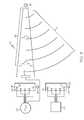
- FIG. 1is a schematic representation of the near-field diffraction from a subwavelength aperture.
- FIG. 2is a block diagram of an embodiment of the present invention depicting sub-wavelength illumination using a metamaterial transmit array.
- FIG. 3is a block diagram of an embodiment of the present invention depicting sub-wavelength illumination and detection using metamaterial transmit and receive arrays.
- FIG. 4is a block diagram of an embodiment of the present invention using amplitude discrimination circuitry.
- FIG. 5is a block diagram of an embodiment of control, conditioning, and processing circuitry of the present invention.
- FIG. 6is a graphical representations of a transmit array focal point and a receive array focal point partially overlapping.
- Sub-wavelength illuminationmeans illuminating a region smaller than the wavelength of the electromagnetic wave being used for the illumination.
- the implication for radar, and in particular ground-penetrating radar (GPR), building penetrating radar (BPR), and metal penetrating radar (MPR),is the ability to obtain a radar return from an area smaller than the size of the radiated wavelength with an appropriately designed lens/antenna which helps localize the radar return.
- the radar return from the sub-wavelength illuminated regioncan also be received and imaged using sub-wavelength imaging techniques in order to achieve new levels of radar resolution. Similar to the way in which time delay is used to phase standard phased array radar antenna elements, time delay can be used in a metamaterial array to change the focal point of the radiation to adjust the depth of a GPR scan or change other features of the array.
- the radar system 10 for producing sub-wavelength illuminationincludes at least one metamaterial transmit array 15 and at least one near-field stimulator or port 20 for inputting an electromagnetic signal 30 to the transmit array so that a sub-wavelength target 35 is illuminated with an electromagnetic wave 40 .
- the transmit array 15includes a plurality of metamaterial elements 45 which form a lens.
- the electromagnetic wavemay have a frequency in the tens of kilohertz range all the way up to optical frequencies in the terahertz range. In some embodiments, the frequency is less than about 1 GHz. In at least one embodiment, the electromagnetic wave has a frequency between about 50 kHz and about 600 MHz, while in other embodiments the frequency is about 100 kHz.
- the near-field stimulator 20is a near-field probe, a port, an antenna, or combination thereof.
- Near-field probesare placed very near to, but not in contact with the metamaterial elements in the transmit array.
- the near-field probesare used to stimulate (in an unmodulated or modulated manner) signals that would be utilized by metamaterial elements to achieve sub-wavelength illumination.
- the near-field probes 55are aligned with a metamaterial element 45 and in operative communication with a sense/exciter/feed array 58 .
- the radar systemincludes an antenna 60 .
- antennacould also be taken as meaning an antenna array.
- the antennamay be placed in front of, behind, to the side of, or inside the lens.
- the antenna 60is used to stimulate the metamaterial elements 45 of the metamaterial transmit array 15 to produce near-field signals.
- the EM signal source 30 and the stimulator 20produce a wave in order to stimulate the metamaterial elements, which produces sub-wavelength illumination.
- both near-field probes or ports and antennas 60are used to stimulate the metamaterial elements in the transmit array, as depicted in FIG. 2 .
- the radar system 10 for producing sub-wavelength illuminationfurther includes at least one metamaterial receive array 65 , constructed and arranged to receive a return wave 70 reflected from an object of interest or target, at least one near-field sensing component 75 , and a far-field filter circuit 80 .
- the return wave 70comprises a near-field component and a far-field component
- the receive arraycomprises a plurality of metamaterial elements 45 forming another lens.
- the near-field sensing component 75is in operative communication with the metamaterial elements 45 of the receive array 65 .
- the sensing components 75can be used to ensure that the array is operating as desired and/or to provide signal(s) to other circuits used to control the performance of the array to ensure the array is operating properly (i.e. feedback to optimize performance).
- the near-field sensing componentmay be a near-field probe, port or a high-impedance probe to sense the near-field and convert it into electrical form, thereby allowing processing of the near-field.
- Electromagnetic signal sourcesare well known in the art.
- an EM signal sourcemay comprise a power source, an oscillator circuit that produces the EM signal, a modulator to control the duration of the signal, and an amplifier to strengthen the EM signal prior to transmission.
- the antenna 60is coupled to the EM signal source 30 typically by a waveguide (not shown) or transmission line (not shown) and the antenna is designed to transmit and/or receive EM signals.
- Dielectric resonatorscan resonate in TM, TE or TM and TE modes.
- TM or TE modesWhen the dielectric resonators are resonant in TM or TE modes then only one effective negative dielectric property (permittivity or permeability) is provided by the resonator so the other effective negative dielectric property is provided by a resonant mode occurring in the spacing between dielectric resonators.
- the third mode/resonance of the cubeis usually a combined TM and TE mode, so that both negative permittivity and negative permeability are provided. This design eliminates any requirements on the spacing between elements and containing the fields within the cube.
- high permittivity materialsare used for one resonant mode and high permeability materials are used for the other resonant mode.
- the high permeability and high permittivity materialsare then combined into one metamaterial cube lens for simultaneous TM/TE mode resonance within the cube.
- the size of the metamaterial elementsmay be dramatically reduced.
- efficiencyis maintained in such a design by matching the wave impedance closely to free space or to the media the metamaterial elements are contained within.
- a 1 ⁇ 2′′ cube of high permittivity material(such as AVX Corporations's X7R dielectric material with a relative permittivity near 3500, available at www.avx.com), is partially enclosed within a cup-shaped or open square design of high permeability interstitial material.
- the permeability of the interstitial materialis matched, as closely as possible, to the permittivity of the dielectric material.
- Such designmay be used at frequencies in the range of about 150 kHz to about 200 kHz.
- SRRSplit Ring Resonators
- wiresAnother way to create a metamaterial is by using Split Ring Resonators (SRR) and wires.
- SRRSplit Ring Resonator structures which are smaller than the size of a wavelength, but resonate in a way which captures and concentrates the near-field evanescent waves are known in the art.
- Proper design of an SRRcauses the effective permeability and permittivity, and thus the refractive index, of a metamaterial to be controllable.
- One method of creating an SRRinvolves two metal disks that form a floating resonant inductor-capacitor (L-C) circuit and wire. The metal disks store electromagnetic energy. The majority of the energy stored in the electric field for the SRR is between the rings and is highest in magnitude close to the gaps in the rings.
- L-Cfloating resonant inductor-capacitor
- the effect of the SRRis amplification or concentration of the near-field/evanescent waves which results in high field strength in the SRR.
- the receive arrayis comprised of a plurality of SRRs, or metamaterial elements 45 , created in an array and forming a circuit.
- each SRRhas an electric field strength between these capacitive plates that can be orders of magnitude larger than the electric fields in the media surrounding the metamaterial.
- metamaterial or electronic band gap insulatorsare used to isolate the metamaterial arrays and simplify their design. Ferrite absorbers, layered media, resistor networks and other techniques are used to help minimize distortions caused by the insulators and to enhance their properties. In some embodiments, absorbers may be used without band-gap or metamaterial insulators.
- the circuit formed by the metamaterial elementsis an integrated circuit/resonator. In at least one embodiment, the circuit formed is a distributed circuit/resonator. In some embodiments, the circuit/resonator is formed by lumped elements and combinations of all the above elements.
- the embodiment shown in FIG. 3includes near-field sensing components 75 .
- the evanescent near-field signalsmay be detected without perturbing the resonating metamaterial.
- near-field sensing techniqueinvolves the use of near-field probes to recover the near-field.
- near-field probesUsed often in SNOM, near-field probes are brought near to a radiating object, without touching it, in order to sense the near-field. Near-field probes scan the radiating object, one pixel at a time, in order to completely reconstruct the object's image. As shown in FIG. 5 , the near-field probes 55 are aligned with a metamaterial element 45 and in operative communication with a sense/exciter/feed array 58 .
- Another embodiment of a near-field sensing techniqueinvolves the use of high-impedance contact probes or at least one transmission line port. Unlike near-field probes, the high-impedance probes and ports make contact with the object being sensed.
- the purpose of the near-field sensing componentsis to sense the near-field and convert it into electrical form. Once converted, the electrical form of the near-field can then be processed, allowing for near-field enhancement and thus improved image resolution.
- a far-field filter circuit 80is included which separates the near-field and the far-field.
- the near-fieldis detected using a far-field metamaterial filter circuit which rejects the far-field, thereby enabling detection of the very low level near-field signal.
- a portion of the metamaterial receive array 65can be designed to filter out frequencies by selecting a relative permittivity or relative permeability to be zero in order to null out the relatively narrow-band spectrum of the far-field and allow discrimination of the wider-band near-field.
- elements, or control components 85such as a varactor, pin diode network, gyrator, load/impedance pull, saturable magnetic, modulaton/frequency control, or other tunable resonator components or sub-circuits, or a combination thereof, may be included in the metamaterial element circuit of the transmit and/or receive arrays in order to allow features of the filter such as the center frequency, focal point and band edges to be tuned.
- the amplitudes of the near-field and the far-fieldcan be compared and used for discrimination.
- the near-field signalis very weak because of its evanescent characteristics. Knowing that the far-field signal has a relatively large amplitude when compared against the near-field signal, and focusing in on a narrow frequency band, the far-field and near-field signals can be discriminated using equalizers, fast Fourier Transform (FFT) techniques, wavelet transform techniques, or other frequency-time filter techniques.
- FFTfast Fourier Transform
- FIG. 4depicts an alternative embodiment for discriminating between the near-field and the far-field, both the near-field and far-field are received by a plurality of frequency selective amplifiers G (or frequency selective attenuators) and detectors or analog-to-digital converters (ADC). The output from the ADCs is fed into an amplitude discrimination circuit 90 .
- Gfrequency selective amplifiers
- ADCanalog-to-digital converters
- an RF front-end stagemay be required prior to ADC detection.
- the front-end stageis used to combine, synchronize (for pulsed systems), and convert the RF frequencies received into signals at lower frequencies that can be processed more readily by a Digital Signal Processor (DSP) and/or other analog and digital circuitry.
- DSPDigital Signal Processor
- a plurality of filters and ADCsis required to provide sub-range resolution. Part of the resolution of each ADC overlaps the previous. If lower level detection is desired, splitting the frequency range into multiple ADCs through the use of filters in order to achieve the noise floor required to enable detection of the near-field signal may be desirable. By enabling the high-fidelity detection of both a far-field signal and the near-field signal, the detection of the near-field superimposed on the far-field is possible, thereby improving the overall resolution of the resulting image. The same technique can be used to detect the entire near-field signal.
- the amplifierscan be low-noise amplifiers or standard amplifiers.
- attenuatorscan also be used, depending upon the return signal amplitudes anticipated and the overlap of each sub-range ADC. In a generalized system, there will be some number N of amplifiers/attenuators, with each being tuned to a different amplitude for lower-level reception. Also, there may be multiple amplifiers combined with filters and/or other signal conditioning circuitry in order to optimize reception.
- the present inventionmay include at least one, or a combination of, components or circuits which perform the following: near-field conditioning 95 , far-field conditioning 100 , near-field RF front-end 105 , far-field RF front-end 110 , near-field processing 115 , far-field processing 120 , and signal combining and processing 125 , in order to produce a composite radar return 126 .
- the far-field conditioningis used for optimizing the power transfer between the antenna array and the RF front end, controlling the direction, beamwidth, bandwidth, center frequency, modulation, squint, polarization, front-to-back ratio, and other features of the antenna array to optimize reception of the far-field and transmission.
- the front-end stageis used to combine, synchronize, and convert the RF frequencies received into signals at lower frequencies that can be processed more readily by a Digital Signal Processor (DSP) and/or other analog and digital circuitry.
- DSPDigital Signal Processor
- Near-field and far-field processingrefers to analog or digital signal processing, which is well-known by those skilled in the art.
- the composite signalis a combination of the near-field and the far field features, resulting in maximized resolution.
- the composite signal(s)is generated from a plurality of signal samples. Most likely a scanning system, or equivalent scanning system via two or more antennas, will be required as in traditional radar imagers (e.g. SNOM applications).
- FIG. 6depicts receive array focal point 140 partially overlapping transmit array focal point 145 at the region 150 .
- receive array focal point 140By not pointing the receive array focal point 140 directly at the transmit array focal point 145 , a smaller portion of the region illuminated by the transmit antenna is sensed by the receive array. In this manner, resolution is improved, but at the expense of power. Sweeping the receive array focal point (or peak gain) versus the transmit array focal point is similar to a technique used in some types of optical sensors to improve image resolution. This method has the added benefit of optimizing the focus of the array in a closed-loop manner.
- a ‘superlens’-like systemcan be used in which the composite signal is generated from only one sample, rather than through scanning.
- a control loopcan ensure that the metamaterial filter is centered on the transmit signal and that the filter rejects the returned far-field.
- the present inventionmay also include circuitry in communication with the metamaterial transmit array, and in some instances with a patch antenna 130 or other antenna array as well.
- the circuitryis designed as a conditioning/combining/control array stage 135 .
- the conditioning/combining/control array stageis circuitry used for detecting the near field signals from a near-field probe, high impedance probe, or other type of contact probe. It may also be used for stimulating metamaterial elements using a near-field probe.
- the conditioning/combining/control array stagecan be used for steering the angle, beamwidth, bandwidth, center frequency, modulation, squint, polarization, focus of the main beam of the metamaterial array for reception or transmission via the use of ports or probes or a separate patch or other antenna array.
- tuning elementssuch as varactors, gyrators, pin diode switched elements, load/impedance pull, saturable magnetics, modulation/frequency control, or other tunable resonator components or sub-circuits, or a combination thereof.
- tuning elementssuch as varactors, gyrators, pin diode switched elements, load/impedance pull, saturable magnetics, modulation/frequency control, or other tunable resonator components or sub-circuits, or
- the present inventioncan be used for improved metal penetrating radar.
- the present inventioncan be used for clutter rejection.
- a far-field returngenerates both a near-field wave and a far-field wave when it diffracts.
- These far-field componentswill appear as clutter noise to a conventional Ground-Penetrating Radar (GPR).
- GPRGround-Penetrating Radar
- these noise components of the far-field returnare similar to the return produced by metamaterials.
- metamaterial elementse.g. resonators
- the return noiseis better defined, thereby allowing significant portions of the return noise to be subtracted out from the far-field return.
- the far-field returncan be processed, thus improving imaging resolution of the object of interest.
- GPRGround-Penetrating Radar
- clutter noisecan be rejected by “seeding” the ground with sub-wavelength sized resonators for controlled diffraction effects.
- the resonatorscan be dispersed on or in the ground near the object to be imaged.
- the resonatorsare preferably optimized to enable detection of a return wave reflected from an object in which the return wave includes dimensional information of the object smaller than the incident wavelength.
- Seedingis also effective in detecting changes in a location in the ground by determining seed locations at the onset of seeding and sensing a change in their locations.
- a baselineis determined by measuring a radar image or signature of a region immediately following placement of seeds. Any disturbances or change in condition in the seeded region can be determined by re-measuring the image or signature and comparing it to the initial radar image or signature.
- the seeded sub-wavelength resonatorsare used to perform the near-to-far field conversion to enhance GPR imaging resolution.
- clutter rejectionis accomplished by narrow-banding, narrow-beaming, modulation techniques, and time domain techniques.
- wide-band metamaterialshave been demonstrated, most metamaterials are narrow-band. Because of their resonant structure, metamaterials can be designed to provide their unique properties over a relatively narrow bandwidth and over relatively narrow angles of incidence.
- a narrow-band antenna/lensis also less susceptible to noise pickup, antenna-ground bounce induced ringing, generates less interference, and is better matched to optimize transmit and receive power to provide a wider dynamic range than is possible with a wideband system.
- Generating the transmit signal for a narrow-band radarhas been demonstrated and is within the state-of-the-art.
- the use of near-field techniques as presented herein to improve the resolution of GPR and Building Penetrating Radar (BPR) and Metal Penetrating Radar (MPR)is novel and inventive.
- Reducing the effective beam width (i.e. narrow-beam) of the GPRalso reduces received artificial and environmental interfering signals and noise, reduces clutter and helps facilitate scanning which is often necessary for near-field techniques.
- a narrow-band modulation techniquee.g. unmodulated wave, Gaussian damped cycle, single cycle, etc.
- may be used in conjunction with knowledge of focal point and ultra-wideband-like techniquese.g. time correlation
- ultra-wideband-like techniquese.g. time correlation
- the sub-wavelength illuminationcan be used for metal penetrating radar.
- sub-wavelength illuminationis not required for metal penetration, as presented earlier, sub-wavelength illumination does improve the resolution of metal penetrating radar. Achieving optimal resolution at metal penetrating frequencies will require a combination of techniques such as sub-wavelength illumination along with the use of near-field sensing components and feedback techniques such as scanning the receive lens focal point across the transmit lens focal point to detect and fine-tune subwavelength focusing.
- the sub-wavelength illuminationcan be used as a directed energy weapon.
- a directed energy weapon using sub-wavelength illumination techniquesis superior to laser systems because of the lower path loss, immunity to cloud cover, immunity to obscuration caused by the burning process and provides the new capability of directed electromagnetic damage.
- Directed electromagnetic damageincludes generating an electromagnetic pulse (EMP) as well as simply producing continuously high localized field strength.
- EMPelectromagnetic pulse
- the electronics in a targetcan be damaged (including situations where the target is EMI/EMP shielded) without damaging the electronics of nearby electronic systems and without requiring the transmit power be as high as that necessary to burn through the walls of the target system (i.e. metal penetrating capability). Circuits designed to protect sensitive electronics from EMP would be ineffective against such a weapon as the sensitive electronics would be exposed directly to high-level electromagnetic fields penetrating the metal enclosure housing the electronics.
- the sub-wavelength illuminationcan be used for clutter rejection.
- the signal to noise of the return signal from the sub-wavelength regionis increased.
- the techniques described above for clutter rejectioncan be used in conjunction with sub-wavelength illumination.
- any dependent claim which followsshould be taken as alternatively written in a multiple dependent form from all prior claims which possess all antecedents referenced in such dependent claim if such multiple dependent format is an accepted format within the jurisdiction (e.g. each claim depending directly from claim 1 should be alternatively taken as depending from all previous claims).
- each claim depending directly from claim 1should be alternatively taken as depending from all previous claims.
- the following dependent claimsshould each be also taken as alternatively written in each singly dependent claim format which creates a dependency from a prior antecedent-possessing claim other than the specific claim listed in such dependent claim below.
Landscapes
- Engineering & Computer Science (AREA)
- Physics & Mathematics (AREA)
- Radar, Positioning & Navigation (AREA)
- Remote Sensing (AREA)
- Electromagnetism (AREA)
- Computer Networks & Wireless Communication (AREA)
- General Physics & Mathematics (AREA)
- Aerials With Secondary Devices (AREA)
- Radar Systems Or Details Thereof (AREA)
Abstract
Description
Claims (18)
Priority Applications (1)
| Application Number | Priority Date | Filing Date | Title |
|---|---|---|---|
| US13/086,713US8587474B2 (en) | 2006-12-15 | 2011-04-14 | Resolution radar using metamaterials |
Applications Claiming Priority (3)
| Application Number | Priority Date | Filing Date | Title |
|---|---|---|---|
| US87532306P | 2006-12-15 | 2006-12-15 | |
| US11/955,795US7928900B2 (en) | 2006-12-15 | 2007-12-13 | Resolution antenna array using metamaterials |
| US13/086,713US8587474B2 (en) | 2006-12-15 | 2011-04-14 | Resolution radar using metamaterials |
Related Parent Applications (1)
| Application Number | Title | Priority Date | Filing Date |
|---|---|---|---|
| US11/955,795ContinuationUS7928900B2 (en) | 2006-12-15 | 2007-12-13 | Resolution antenna array using metamaterials |
Publications (2)
| Publication Number | Publication Date |
|---|---|
| US20110187577A1 US20110187577A1 (en) | 2011-08-04 |
| US8587474B2true US8587474B2 (en) | 2013-11-19 |
Family
ID=40669257
Family Applications (2)
| Application Number | Title | Priority Date | Filing Date |
|---|---|---|---|
| US11/955,795Active2028-09-02US7928900B2 (en) | 2006-12-15 | 2007-12-13 | Resolution antenna array using metamaterials |
| US13/086,713ActiveUS8587474B2 (en) | 2006-12-15 | 2011-04-14 | Resolution radar using metamaterials |
Family Applications Before (1)
| Application Number | Title | Priority Date | Filing Date |
|---|---|---|---|
| US11/955,795Active2028-09-02US7928900B2 (en) | 2006-12-15 | 2007-12-13 | Resolution antenna array using metamaterials |
Country Status (1)
| Country | Link |
|---|---|
| US (2) | US7928900B2 (en) |
Cited By (8)
| Publication number | Priority date | Publication date | Assignee | Title |
|---|---|---|---|---|
| US20160146731A1 (en)* | 2013-06-26 | 2016-05-26 | Korea Advanced Institute Of Science And Technology | Method and Apparatus for Manipulating Near Field Using Light Scattering |
| US20200319331A1 (en)* | 2019-04-04 | 2020-10-08 | Battelle Memorial Institute | Imaging Systems and Related Methods Including Radar Imaging with Moving Arrays or Moving Targets |
| US11133577B2 (en)* | 2018-05-24 | 2021-09-28 | Metawave Corporation | Intelligent meta-structure antennas with targeted polarization for object identification |
| US11221394B2 (en)* | 2017-12-15 | 2022-01-11 | Google Llc | Radar attenuation mitigation |
| US11579456B2 (en)* | 2017-08-31 | 2023-02-14 | Metalenz, Inc. | Transmissive metasurface lens integration |
| US11927769B2 (en) | 2022-03-31 | 2024-03-12 | Metalenz, Inc. | Polarization sorting metasurface microlens array device |
| US11978752B2 (en) | 2019-07-26 | 2024-05-07 | Metalenz, Inc. | Aperture-metasurface and hybrid refractive-metasurface imaging systems |
| US12140778B2 (en) | 2018-07-02 | 2024-11-12 | Metalenz, Inc. | Metasurfaces for laser speckle reduction |
Families Citing this family (80)
| Publication number | Priority date | Publication date | Assignee | Title |
|---|---|---|---|---|
| US7928900B2 (en)* | 2006-12-15 | 2011-04-19 | Alliant Techsystems Inc. | Resolution antenna array using metamaterials |
| DE102007016588B4 (en)* | 2007-04-05 | 2014-10-09 | Fraunhofer-Gesellschaft zur Förderung der angewandten Forschung e.V. | Sub-wavelength resolution microscope and method for generating an image of an object |
| US7733289B2 (en)* | 2007-10-31 | 2010-06-08 | The Invention Science Fund I, Llc | Electromagnetic compression apparatus, methods, and systems |
| US20090218524A1 (en)* | 2008-02-29 | 2009-09-03 | Searete Llc, A Limited Liability Corporation Of The State Of Delaware | Electromagnetic cloaking and translation apparatus, methods, and systems |
| US20090218523A1 (en)* | 2008-02-29 | 2009-09-03 | Searete Llc, A Limited Liability Corporation Of The State Of Delaware | Electromagnetic cloaking and translation apparatus, methods, and systems |
| US8487832B2 (en)* | 2008-03-12 | 2013-07-16 | The Boeing Company | Steering radio frequency beams using negative index metamaterial lenses |
| US8493281B2 (en)* | 2008-03-12 | 2013-07-23 | The Boeing Company | Lens for scanning angle enhancement of phased array antennas |
| US7928892B2 (en)* | 2008-05-07 | 2011-04-19 | The Boeing Company | Identification and mapping of underground facilities |
| US8638504B2 (en)* | 2008-05-30 | 2014-01-28 | The Invention Science Fund I Llc | Emitting and negatively-refractive focusing apparatus, methods, and systems |
| US9019632B2 (en)* | 2008-05-30 | 2015-04-28 | The Invention Science Fund I Llc | Negatively-refractive focusing and sensing apparatus, methods, and systems |
| US8164837B2 (en)* | 2008-05-30 | 2012-04-24 | The Invention Science Fund I, Llc | Negatively-refractive focusing and sensing apparatus, methods, and systems |
| US8773776B2 (en)* | 2008-05-30 | 2014-07-08 | The Invention Science Fund I Llc | Emitting and negatively-refractive focusing apparatus, methods, and systems |
| US8531782B2 (en)* | 2008-05-30 | 2013-09-10 | The Invention Science Fund I Llc | Emitting and focusing apparatus, methods, and systems |
| US8817380B2 (en)* | 2008-05-30 | 2014-08-26 | The Invention Science Fund I Llc | Emitting and negatively-refractive focusing apparatus, methods, and systems |
| US8736982B2 (en) | 2008-05-30 | 2014-05-27 | The Invention Science Fund I Llc | Emitting and focusing apparatus, methods, and systems |
| US8493669B2 (en) | 2008-05-30 | 2013-07-23 | The Invention Science Fund I Llc | Focusing and sensing apparatus, methods, and systems |
| US8773775B2 (en) | 2008-05-30 | 2014-07-08 | The Invention Science Fund I Llc | Emitting and negatively-refractive focusing apparatus, methods, and systems |
| US8837058B2 (en)* | 2008-07-25 | 2014-09-16 | The Invention Science Fund I Llc | Emitting and negatively-refractive focusing apparatus, methods, and systems |
| US8730591B2 (en)* | 2008-08-07 | 2014-05-20 | The Invention Science Fund I Llc | Negatively-refractive focusing and sensing apparatus, methods, and systems |
| KR20170056019A (en) | 2008-08-22 | 2017-05-22 | 듀크 유니버시티 | Metamaterials for surfaces and waveguides |
| US8723722B2 (en) | 2008-08-28 | 2014-05-13 | Alliant Techsystems Inc. | Composites for antennas and other applications |
| US9081123B2 (en)* | 2009-04-17 | 2015-07-14 | The Invention Science Fund I Llc | Evanescent electromagnetic wave conversion lenses II |
| US9083082B2 (en)* | 2009-04-17 | 2015-07-14 | The Invention Science Fund I Llc | Evanescent electromagnetic wave conversion lenses III |
| US9081202B2 (en)* | 2009-04-17 | 2015-07-14 | The Invention Science Fund I Llc | Evanescent electromagnetic wave conversion lenses I |
| US8487808B2 (en)* | 2009-06-30 | 2013-07-16 | Mitsubishi Electric Research Laboratories, Inc. | High resolution SAR imaging using non-uniform pulse timing |
| KR101278030B1 (en)* | 2009-12-08 | 2013-06-21 | 숭실대학교산학협력단 | Low Phase Noise voltage-controlled oscillator Using High-Quality Factor Metamaterial Transmission Line |
| KR101706693B1 (en)* | 2009-12-30 | 2017-02-14 | 삼성전자주식회사 | Wireless power transmission apparatus using near field focusing |
| US8350777B2 (en)* | 2010-02-18 | 2013-01-08 | Raytheon Company | Metamaterial radome/isolator |
| US8988759B2 (en) | 2010-07-26 | 2015-03-24 | The Invention Science Fund I Llc | Metamaterial surfaces |
| US8830114B2 (en)* | 2010-09-30 | 2014-09-09 | Toyota Jidosha Kabushiki Kaisha | Mobile object detecting apparatus |
| EP2702697A1 (en)* | 2011-04-28 | 2014-03-05 | Alliant Techsystems Inc. | Devices for wireless energy transmission using near -field energy |
| US9054491B1 (en) | 2012-02-10 | 2015-06-09 | Walter C. Hurlbut | Solid-state coherent electromagnetic radiation source |
| KR20150042746A (en) | 2012-05-09 | 2015-04-21 | 듀크 유니버시티 | Metamaterial devices and methods of using the same |
| US9411042B2 (en) | 2012-05-09 | 2016-08-09 | Duke University | Multi-sensor compressive imaging |
| US10534189B2 (en)* | 2012-11-27 | 2020-01-14 | The Board Of Trustees Of The Leland Stanford Junior University | Universal linear components |
| US9980114B2 (en) | 2013-03-15 | 2018-05-22 | Elwha Llc | Systems and methods for communication management |
| US9876762B2 (en)* | 2012-12-31 | 2018-01-23 | Elwha Llc | Cost-effective mobile connectivity protocols |
| US9781664B2 (en) | 2012-12-31 | 2017-10-03 | Elwha Llc | Cost-effective mobile connectivity protocols |
| US8965288B2 (en) | 2012-12-31 | 2015-02-24 | Elwha Llc | Cost-effective mobile connectivity protocols |
| US9635605B2 (en) | 2013-03-15 | 2017-04-25 | Elwha Llc | Protocols for facilitating broader access in wireless communications |
| US9713013B2 (en) | 2013-03-15 | 2017-07-18 | Elwha Llc | Protocols for providing wireless communications connectivity maps |
| US9832628B2 (en)* | 2012-12-31 | 2017-11-28 | Elwha, Llc | Cost-effective mobile connectivity protocols |
| US9451394B2 (en) | 2012-12-31 | 2016-09-20 | Elwha Llc | Cost-effective mobile connectivity protocols |
| US9706060B2 (en) | 2013-03-15 | 2017-07-11 | Elwha Llc | Protocols for facilitating broader access in wireless communications |
| US9781554B2 (en) | 2013-03-15 | 2017-10-03 | Elwha Llc | Protocols for facilitating third party authorization for a rooted communication device in wireless communications |
| US9813887B2 (en) | 2013-03-15 | 2017-11-07 | Elwha Llc | Protocols for facilitating broader access in wireless communications responsive to charge authorization statuses |
| US9807582B2 (en) | 2013-03-15 | 2017-10-31 | Elwha Llc | Protocols for facilitating broader access in wireless communications |
| US9843917B2 (en) | 2013-03-15 | 2017-12-12 | Elwha, Llc | Protocols for facilitating charge-authorized connectivity in wireless communications |
| US9706382B2 (en) | 2013-03-15 | 2017-07-11 | Elwha Llc | Protocols for allocating communication services cost in wireless communications |
| US9693214B2 (en) | 2013-03-15 | 2017-06-27 | Elwha Llc | Protocols for facilitating broader access in wireless communications |
| US9596584B2 (en) | 2013-03-15 | 2017-03-14 | Elwha Llc | Protocols for facilitating broader access in wireless communications by conditionally authorizing a charge to an account of a third party |
| US9866706B2 (en) | 2013-03-15 | 2018-01-09 | Elwha Llc | Protocols for facilitating broader access in wireless communications |
| WO2015054601A2 (en)* | 2013-10-11 | 2015-04-16 | Duke University | Multi-sensor compressive imaging |
| WO2015152758A1 (en)* | 2014-04-02 | 2015-10-08 | Baker Hughes Incorporated | Imaging of earth formation with high frequency sensor |
| WO2015181818A1 (en)* | 2014-05-27 | 2015-12-03 | Technion Research & Development Foundation Limited. | Near-field imaging devices |
| CN104237856B (en)* | 2014-09-28 | 2016-10-05 | 贵州航天计量测试技术研究所 | A kind of radar detection signal high precision time delay generator and control method |
| WO2016057115A1 (en) | 2014-10-09 | 2016-04-14 | Utc Fire & Security Corporation | Device for providing wireless energy transfer |
| CN104965203B (en)* | 2015-05-25 | 2017-06-16 | 北京理工雷科电子信息技术有限公司 | A kind of target has an X-rayed radar imaging method |
| US10236576B2 (en) | 2015-09-04 | 2019-03-19 | Elwha Llc | Wireless power transfer using tunable metamaterial systems and methods |
| US10218067B2 (en)* | 2015-09-04 | 2019-02-26 | Elwha Llc | Tunable metamaterial systems and methods |
| US10374669B2 (en) | 2016-08-31 | 2019-08-06 | Elwha Llc | Tunable medium linear coder |
| CN106443674B (en)* | 2016-09-23 | 2019-03-22 | 中国地质大学(武汉) | A kind of Ground Penetrating Radar Velocity Estimation based on diffraction and imaging and minimum entropy technique |
| US10763290B2 (en)* | 2017-02-22 | 2020-09-01 | Elwha Llc | Lidar scanning system |
| US10359513B2 (en) | 2017-05-03 | 2019-07-23 | Elwha Llc | Dynamic-metamaterial coded-aperture imaging |
| US10468776B2 (en)* | 2017-05-04 | 2019-11-05 | Elwha Llc | Medical applications using tunable metamaterial systems and methods |
| US10249950B1 (en) | 2017-09-16 | 2019-04-02 | Searete Llc | Systems and methods for reduced control inputs in tunable meta-devices |
| US10833381B2 (en) | 2017-11-08 | 2020-11-10 | The Invention Science Fund I Llc | Metamaterial phase shifters |
| CN108413991B (en)* | 2018-02-12 | 2020-11-06 | 深圳市建讯电子有限公司 | Method and device for detecting proximity of metal coil/plate in electromagnetic wave transmission process |
| US11450953B2 (en) | 2018-03-25 | 2022-09-20 | Metawave Corporation | Meta-structure antenna array |
| US11424548B2 (en) | 2018-05-01 | 2022-08-23 | Metawave Corporation | Method and apparatus for a meta-structure antenna array |
| US11342682B2 (en) | 2018-05-24 | 2022-05-24 | Metawave Corporation | Frequency-selective reflector module and system |
| US11385326B2 (en) | 2018-06-13 | 2022-07-12 | Metawave Corporation | Hybrid analog and digital beamforming |
| US10771124B2 (en) | 2018-06-14 | 2020-09-08 | Jun Fang | Virtual beam steering using MIMO radar |
| US11555918B2 (en) | 2018-08-17 | 2023-01-17 | Metawave Corporation | Method and apparatus for radar system |
| US12102420B2 (en) | 2018-10-03 | 2024-10-01 | Arizona Board Of Regents On Behalf Of Arizona State University | Direct RF signal processing for heart-rate monitoring using UWB impulse radar |
| US11994609B2 (en) | 2018-11-16 | 2024-05-28 | Bdcm A2 Llc | Method and apparatus for coded radar signals |
| US11741807B2 (en) | 2018-11-21 | 2023-08-29 | Frederick Lee Newton | Methods and apparatus for a public area defense system |
| US11879706B2 (en) | 2019-01-28 | 2024-01-23 | Frederick Lee Newton | Methods and apparatus for non-lethal weapons comprising a power amplifier to produce a nonlethal beam of energy |
| WO2021087337A1 (en)* | 2019-11-01 | 2021-05-06 | Arizona Board Of Regents On Behalf Of Arizona State University | Remote recovery of acoustic signals from passive sources |
| WO2021133408A1 (en)* | 2019-12-27 | 2021-07-01 | Intel Corporation | Embedded antennas structures for wireless communications and radar |
Citations (52)
| Publication number | Priority date | Publication date | Assignee | Title |
|---|---|---|---|---|
| US649621A (en) | 1897-09-02 | 1900-05-15 | Nikola Tesla | Apparatus for transmission of electrical energy. |
| US685958A (en) | 1901-03-21 | 1901-11-05 | Nikola Tesla | Method of utilizing radiant energy. |
| US3535543A (en) | 1969-05-01 | 1970-10-20 | Nasa | Microwave power receiving antenna |
| US3933323A (en) | 1974-03-20 | 1976-01-20 | Raytheon Company | Solid state solar to microwave energy converter system and apparatus |
| US4078747A (en) | 1974-08-13 | 1978-03-14 | Phaser Telepropulsion, Inc. | Orbiting solar power station |
| US4955562A (en) | 1987-11-24 | 1990-09-11 | Her Majesty The Queen In Right Of Canada, As Represented By The Minister Of Communications | Microwave powered aircraft |
| US5633972A (en) | 1995-11-29 | 1997-05-27 | Trustees Of Tufts College | Superresolution imaging fiber for subwavelength light energy generation and near-field optical microscopy |
| US6181293B1 (en) | 1998-01-08 | 2001-01-30 | E*Star, Inc. | Reflector based dielectric lens antenna system including bifocal lens |
| US6621448B1 (en)* | 2002-04-05 | 2003-09-16 | The Regents Of The University Of California | Non-contact radar system for reconstruction of scenes obscured under snow and similar material |
| US6661392B2 (en) | 2001-08-17 | 2003-12-09 | Lucent Technologies Inc. | Resonant antennas |
| US6731248B2 (en) | 2002-06-27 | 2004-05-04 | Harris Corporation | High efficiency printed circuit array of log-periodic dipole arrays |
| US6734827B2 (en) | 2002-06-27 | 2004-05-11 | Harris Corporation | High efficiency printed circuit LPDA |
| US20040164915A1 (en) | 2003-02-25 | 2004-08-26 | Clifton Quan | Wideband 2-D electronically scanned array with compact CTS feed and MEMS phase shifters |
| US6938325B2 (en) | 2003-01-31 | 2005-09-06 | The Boeing Company | Methods of fabricating electromagnetic meta-materials |
| US20050225492A1 (en) | 2004-03-05 | 2005-10-13 | Carsten Metz | Phased array metamaterial antenna system |
| US20060028385A1 (en) | 2004-08-05 | 2006-02-09 | Davis Mark R | Metamaterial scanning lens antenna systems and methods |
| US7015865B2 (en)* | 2004-03-10 | 2006-03-21 | Lucent Technologies Inc. | Media with controllable refractive properties |
| US20060266917A1 (en) | 2005-05-23 | 2006-11-30 | Baldis Sisinio F | Wireless Power Transmission System |
| US20070057852A1 (en) | 2005-09-15 | 2007-03-15 | Motorola, Inc. | Wireless communication device with integrated antenna |
| US20070138402A1 (en) | 2005-12-21 | 2007-06-21 | Searete Llc, A Limited Liability Corporation Of The State Of Delaware | Variable multi-stage waveform detector |
| US7256753B2 (en) | 2003-01-14 | 2007-08-14 | The Penn State Research Foundation | Synthesis of metamaterial ferrites for RF applications using electromagnetic bandgap structures |
| US7301493B1 (en) | 2005-11-21 | 2007-11-27 | The United States Of America As Represented By The Secretary Of The Army | Meta-materials based upon surface coupling phenomena to achieve one-way mirror for various electro-magnetic signals |
| US20080001684A1 (en) | 2006-05-18 | 2008-01-03 | The Regents Of The University Of California | Power combiners using meta-material composite right/left hand transmission line at infinite wavelength frequency |
| US20080014897A1 (en) | 2006-01-18 | 2008-01-17 | Cook Nigel P | Method and apparatus for delivering energy to an electrical or electronic device via a wireless link |
| US20090015075A1 (en) | 2007-07-09 | 2009-01-15 | Nigel Power, Llc | Wireless Energy Transfer Using Coupled Antennas |
| US7525711B1 (en) | 2005-08-31 | 2009-04-28 | The United States Of America As Represented By The Secretary Of The Navy | Actively tunable electromagnetic metamaterial |
| US20090135086A1 (en) | 2006-12-15 | 2009-05-28 | Alliant Techsystems Inc. | Resolution radar using metamaterials |
| US20100033021A1 (en) | 2008-08-05 | 2010-02-11 | Broadcom Corporation | Phased array wireless resonant power delivery system |
| US20100039234A1 (en) | 2008-08-15 | 2010-02-18 | Ivi Smart Technologies, Inc. | Rf power conversion circuits & methods, both for use in mobile devices |
| US20100109445A1 (en) | 2008-09-27 | 2010-05-06 | Kurs Andre B | Wireless energy transfer systems |
| US20100123530A1 (en) | 2008-11-17 | 2010-05-20 | Samsung Electronics Co., Ltd. | Apparatus for wireless power transmission using high Q low frequency near magnetic field resonator |
| US7724180B2 (en)* | 2007-05-04 | 2010-05-25 | Toyota Motor Corporation | Radar system with an active lens for adjustable field of view |
| US7728772B2 (en) | 2006-06-09 | 2010-06-01 | The Regents Of The University Of Michigan | Phased array systems and phased array front-end devices |
| US7733265B2 (en)* | 2008-04-04 | 2010-06-08 | Toyota Motor Engineering & Manufacturing North America, Inc. | Three dimensional integrated automotive radars and methods of manufacturing the same |
| US20100148589A1 (en) | 2008-10-01 | 2010-06-17 | Hamam Rafif E | Efficient near-field wireless energy transfer using adiabatic system variations |
| US7741734B2 (en) | 2005-07-12 | 2010-06-22 | Massachusetts Institute Of Technology | Wireless non-radiative energy transfer |
| US20100164296A1 (en) | 2008-09-27 | 2010-07-01 | Kurs Andre B | Wireless energy transfer using variable size resonators and system monitoring |
| US20100164297A1 (en) | 2008-09-27 | 2010-07-01 | Kurs Andre B | Wireless energy transfer using conducting surfaces to shape fields and reduce loss |
| US20100164298A1 (en) | 2008-09-27 | 2010-07-01 | Aristeidis Karalis | Wireless energy transfer using magnetic materials to shape field and reduce loss |
| US20100171368A1 (en) | 2008-09-27 | 2010-07-08 | Schatz David A | Wireless energy transfer with frequency hopping |
| US20100181845A1 (en) | 2008-09-27 | 2010-07-22 | Ron Fiorello | Temperature compensation in a wireless transfer system |
| US20100201203A1 (en) | 2008-09-27 | 2010-08-12 | Schatz David A | Wireless energy transfer with feedback control for lighting applications |
| US20100219694A1 (en) | 2008-09-27 | 2010-09-02 | Kurs Andre B | Wireless energy transfer in lossy environments |
| US7791355B1 (en) | 2007-10-30 | 2010-09-07 | The United States Of America As Represented By The Secretary Of The Air Force | Near field free space anisotropic materials characterization |
| US20100231340A1 (en) | 2008-09-27 | 2010-09-16 | Ron Fiorello | Wireless energy transfer resonator enclosures |
| US20100237709A1 (en) | 2008-09-27 | 2010-09-23 | Hall Katherine L | Resonator arrays for wireless energy transfer |
| US20100259110A1 (en) | 2008-09-27 | 2010-10-14 | Kurs Andre B | Resonator optimizations for wireless energy transfer |
| US20100259108A1 (en) | 2008-09-27 | 2010-10-14 | Giler Eric R | Wireless energy transfer using repeater resonators |
| US20100264747A1 (en) | 2008-09-27 | 2010-10-21 | Hall Katherine L | Wireless energy transfer converters |
| US20100277387A1 (en) | 2004-12-21 | 2010-11-04 | Q-Track Corporation | Space Efficient Magnetic Antenna Method |
| US20100277121A1 (en) | 2008-09-27 | 2010-11-04 | Hall Katherine L | Wireless energy transfer between a source and a vehicle |
| US20100289342A1 (en) | 2009-05-12 | 2010-11-18 | William Eugene Maness | Space-Based Power Systems And Methods |
- 2007
- 2007-12-13USUS11/955,795patent/US7928900B2/enactiveActive
- 2011
- 2011-04-14USUS13/086,713patent/US8587474B2/enactiveActive
Patent Citations (56)
| Publication number | Priority date | Publication date | Assignee | Title |
|---|---|---|---|---|
| US649621A (en) | 1897-09-02 | 1900-05-15 | Nikola Tesla | Apparatus for transmission of electrical energy. |
| US685958A (en) | 1901-03-21 | 1901-11-05 | Nikola Tesla | Method of utilizing radiant energy. |
| US3535543A (en) | 1969-05-01 | 1970-10-20 | Nasa | Microwave power receiving antenna |
| US3933323A (en) | 1974-03-20 | 1976-01-20 | Raytheon Company | Solid state solar to microwave energy converter system and apparatus |
| US4078747A (en) | 1974-08-13 | 1978-03-14 | Phaser Telepropulsion, Inc. | Orbiting solar power station |
| US4955562A (en) | 1987-11-24 | 1990-09-11 | Her Majesty The Queen In Right Of Canada, As Represented By The Minister Of Communications | Microwave powered aircraft |
| US5633972A (en) | 1995-11-29 | 1997-05-27 | Trustees Of Tufts College | Superresolution imaging fiber for subwavelength light energy generation and near-field optical microscopy |
| US6181293B1 (en) | 1998-01-08 | 2001-01-30 | E*Star, Inc. | Reflector based dielectric lens antenna system including bifocal lens |
| US6661392B2 (en) | 2001-08-17 | 2003-12-09 | Lucent Technologies Inc. | Resonant antennas |
| US6621448B1 (en)* | 2002-04-05 | 2003-09-16 | The Regents Of The University Of California | Non-contact radar system for reconstruction of scenes obscured under snow and similar material |
| US6731248B2 (en) | 2002-06-27 | 2004-05-04 | Harris Corporation | High efficiency printed circuit array of log-periodic dipole arrays |
| US6734827B2 (en) | 2002-06-27 | 2004-05-11 | Harris Corporation | High efficiency printed circuit LPDA |
| US7256753B2 (en) | 2003-01-14 | 2007-08-14 | The Penn State Research Foundation | Synthesis of metamaterial ferrites for RF applications using electromagnetic bandgap structures |
| US6938325B2 (en) | 2003-01-31 | 2005-09-06 | The Boeing Company | Methods of fabricating electromagnetic meta-materials |
| US20040164915A1 (en) | 2003-02-25 | 2004-08-26 | Clifton Quan | Wideband 2-D electronically scanned array with compact CTS feed and MEMS phase shifters |
| US6958729B1 (en) | 2004-03-05 | 2005-10-25 | Lucent Technologies Inc. | Phased array metamaterial antenna system |
| US20050225492A1 (en) | 2004-03-05 | 2005-10-13 | Carsten Metz | Phased array metamaterial antenna system |
| US7015865B2 (en)* | 2004-03-10 | 2006-03-21 | Lucent Technologies Inc. | Media with controllable refractive properties |
| US20060028385A1 (en) | 2004-08-05 | 2006-02-09 | Davis Mark R | Metamaterial scanning lens antenna systems and methods |
| US7218285B2 (en) | 2004-08-05 | 2007-05-15 | The Boeing Company | Metamaterial scanning lens antenna systems and methods |
| US20100277387A1 (en) | 2004-12-21 | 2010-11-04 | Q-Track Corporation | Space Efficient Magnetic Antenna Method |
| US20060266917A1 (en) | 2005-05-23 | 2006-11-30 | Baldis Sisinio F | Wireless Power Transmission System |
| US7741734B2 (en) | 2005-07-12 | 2010-06-22 | Massachusetts Institute Of Technology | Wireless non-radiative energy transfer |
| US7525711B1 (en) | 2005-08-31 | 2009-04-28 | The United States Of America As Represented By The Secretary Of The Navy | Actively tunable electromagnetic metamaterial |
| US20070057852A1 (en) | 2005-09-15 | 2007-03-15 | Motorola, Inc. | Wireless communication device with integrated antenna |
| US7301493B1 (en) | 2005-11-21 | 2007-11-27 | The United States Of America As Represented By The Secretary Of The Army | Meta-materials based upon surface coupling phenomena to achieve one-way mirror for various electro-magnetic signals |
| US20070138402A1 (en) | 2005-12-21 | 2007-06-21 | Searete Llc, A Limited Liability Corporation Of The State Of Delaware | Variable multi-stage waveform detector |
| US20080014897A1 (en) | 2006-01-18 | 2008-01-17 | Cook Nigel P | Method and apparatus for delivering energy to an electrical or electronic device via a wireless link |
| US20080001684A1 (en) | 2006-05-18 | 2008-01-03 | The Regents Of The University Of California | Power combiners using meta-material composite right/left hand transmission line at infinite wavelength frequency |
| US7728772B2 (en) | 2006-06-09 | 2010-06-01 | The Regents Of The University Of Michigan | Phased array systems and phased array front-end devices |
| US20090135086A1 (en) | 2006-12-15 | 2009-05-28 | Alliant Techsystems Inc. | Resolution radar using metamaterials |
| US7724180B2 (en)* | 2007-05-04 | 2010-05-25 | Toyota Motor Corporation | Radar system with an active lens for adjustable field of view |
| US20090015075A1 (en) | 2007-07-09 | 2009-01-15 | Nigel Power, Llc | Wireless Energy Transfer Using Coupled Antennas |
| US7791355B1 (en) | 2007-10-30 | 2010-09-07 | The United States Of America As Represented By The Secretary Of The Air Force | Near field free space anisotropic materials characterization |
| US7733265B2 (en)* | 2008-04-04 | 2010-06-08 | Toyota Motor Engineering & Manufacturing North America, Inc. | Three dimensional integrated automotive radars and methods of manufacturing the same |
| US20100033021A1 (en) | 2008-08-05 | 2010-02-11 | Broadcom Corporation | Phased array wireless resonant power delivery system |
| US20100039234A1 (en) | 2008-08-15 | 2010-02-18 | Ivi Smart Technologies, Inc. | Rf power conversion circuits & methods, both for use in mobile devices |
| US20100237709A1 (en) | 2008-09-27 | 2010-09-23 | Hall Katherine L | Resonator arrays for wireless energy transfer |
| US20100219694A1 (en) | 2008-09-27 | 2010-09-02 | Kurs Andre B | Wireless energy transfer in lossy environments |
| US20100164296A1 (en) | 2008-09-27 | 2010-07-01 | Kurs Andre B | Wireless energy transfer using variable size resonators and system monitoring |
| US20100164297A1 (en) | 2008-09-27 | 2010-07-01 | Kurs Andre B | Wireless energy transfer using conducting surfaces to shape fields and reduce loss |
| US20100164298A1 (en) | 2008-09-27 | 2010-07-01 | Aristeidis Karalis | Wireless energy transfer using magnetic materials to shape field and reduce loss |
| US20100171368A1 (en) | 2008-09-27 | 2010-07-08 | Schatz David A | Wireless energy transfer with frequency hopping |
| US20100181843A1 (en) | 2008-09-27 | 2010-07-22 | Schatz David A | Wireless energy transfer for refrigerator application |
| US20100181845A1 (en) | 2008-09-27 | 2010-07-22 | Ron Fiorello | Temperature compensation in a wireless transfer system |
| US20100201203A1 (en) | 2008-09-27 | 2010-08-12 | Schatz David A | Wireless energy transfer with feedback control for lighting applications |
| US20100277121A1 (en) | 2008-09-27 | 2010-11-04 | Hall Katherine L | Wireless energy transfer between a source and a vehicle |
| US20100141042A1 (en) | 2008-09-27 | 2010-06-10 | Kesler Morris P | Wireless energy transfer systems |
| US20100231340A1 (en) | 2008-09-27 | 2010-09-16 | Ron Fiorello | Wireless energy transfer resonator enclosures |
| US20100109445A1 (en) | 2008-09-27 | 2010-05-06 | Kurs Andre B | Wireless energy transfer systems |
| US20100259110A1 (en) | 2008-09-27 | 2010-10-14 | Kurs Andre B | Resonator optimizations for wireless energy transfer |
| US20100259108A1 (en) | 2008-09-27 | 2010-10-14 | Giler Eric R | Wireless energy transfer using repeater resonators |
| US20100264747A1 (en) | 2008-09-27 | 2010-10-21 | Hall Katherine L | Wireless energy transfer converters |
| US20100148589A1 (en) | 2008-10-01 | 2010-06-17 | Hamam Rafif E | Efficient near-field wireless energy transfer using adiabatic system variations |
| US20100123530A1 (en) | 2008-11-17 | 2010-05-20 | Samsung Electronics Co., Ltd. | Apparatus for wireless power transmission using high Q low frequency near magnetic field resonator |
| US20100289342A1 (en) | 2009-05-12 | 2010-11-18 | William Eugene Maness | Space-Based Power Systems And Methods |
Non-Patent Citations (13)
| Title |
|---|
| "How Metamaterials Will Boost Wireless Power Transmission" The Physics arXiv Blog, © 2011 MIT Technology Review. |
| A. Karalis et al., "Efficient wireless non-radiative mid-range energy transfer", Annals of Physics 323 (2008) 34-48. |
| Chew et al., "Elastic scattering of evanescent electromagnetic waves", Applied Optics, vol. 18, No. 15, Aug. 1979, pp. 2679-2687. |
| David Smith, "Superlens breaks optical barrier", Physics Web, Aug. 2005, http://www.physicsweb.org/articles/world/18/8/4. |
| International Search Report mailed Dec. 20, 2011 for PCT Application No. PCT/US11/56870, filed Oct. 19, 2011. |
| J.B. Pendry, A.J. Holden, D.J. Robbins, and W.J. Stewart, "Magnetism from Conductors and Enhanced Nonlinear Phenomena", IEEE Trans. Microwave Theory Tech., vol. 47, No. 11, pp. 2075-2084, Nov. 1999. |
| Jaewon Kim and Anand Gopinath, "Application of Cubic High Dielectric Resonator Metamaterial to Antennas", presented in session 220 at IEE Antenna and Propagation Society conference in Jun. 2007. |
| N. Fang, X. Zhang, "Imaging Properties of a Metamaterial Superlens", Appl. Phys. Lett., vol. 82, No. 2, pp. 161-163, Jan. 2003; 23. Nassenstein, A. Phys. Lett. 29a, 175 (1969). |
| Rebecca Boyle, "Metamaterial Lenses Could Allow Easy Wireless Power Transmission", May 23, 2011, Copyright © 2009 Popular Science. |
| T.W. Ebbesen, H.J. Lezec, H.F. Ghaemi, T. Thio, P.A. Wolff, "Extraordinary Optical Transmission through Sub-Wavelength Hole Arrays", Nature, vol. 391, pp. 667-669, 1998. |
| Wolf, E. and Nieto-Vesperinas, "Analyticity of the angular spectrum amplitude of scattered fields and some of its consequences", J. Opt. Soc. Am. A, vol. 2, No. 6, 886-890 (Jun. 1985). |
| Written Opinion mailed Dec. 20, 2011 for PCT Application No. PCT/US11/56870, filed Oct. 19, 2011. |
| Yaroslav Urzhumov et al., "Metamaterial-Enhanced Coupling between Magnetic Dipoles for Efficient Wireless Power Transfer" [physics.class-ph] pp. 1-23, Feb. 11, 2011. |
Cited By (16)
| Publication number | Priority date | Publication date | Assignee | Title |
|---|---|---|---|---|
| US9857302B2 (en)* | 2013-06-26 | 2018-01-02 | Korea Advanced Institute Of Science And Technology | Method and apparatus for manipulating near field using light scattering |
| US20160146731A1 (en)* | 2013-06-26 | 2016-05-26 | Korea Advanced Institute Of Science And Technology | Method and Apparatus for Manipulating Near Field Using Light Scattering |
| US11988844B2 (en) | 2017-08-31 | 2024-05-21 | Metalenz, Inc. | Transmissive metasurface lens integration |
| US12411348B2 (en) | 2017-08-31 | 2025-09-09 | Metalenz, Inc. | Transmissive metasurface lens integration |
| US11579456B2 (en)* | 2017-08-31 | 2023-02-14 | Metalenz, Inc. | Transmissive metasurface lens integration |
| US11221394B2 (en)* | 2017-12-15 | 2022-01-11 | Google Llc | Radar attenuation mitigation |
| US11133577B2 (en)* | 2018-05-24 | 2021-09-28 | Metawave Corporation | Intelligent meta-structure antennas with targeted polarization for object identification |
| US12140778B2 (en) | 2018-07-02 | 2024-11-12 | Metalenz, Inc. | Metasurfaces for laser speckle reduction |
| US12026907B2 (en)* | 2019-04-04 | 2024-07-02 | Battelle Memorial Institute | Imaging systems and related methods including radar imaging with moving arrays or moving targets |
| US12106506B2 (en) | 2019-04-04 | 2024-10-01 | Battelle Memorial Institute | Imaging systems and related methods including radar imaging with moving arrays or moving targets |
| US11715228B2 (en) | 2019-04-04 | 2023-08-01 | Battelle Memorial Institute | Imaging systems and related methods including radar imaging with moving arrays or moving targets |
| US20200319331A1 (en)* | 2019-04-04 | 2020-10-08 | Battelle Memorial Institute | Imaging Systems and Related Methods Including Radar Imaging with Moving Arrays or Moving Targets |
| US11978752B2 (en) | 2019-07-26 | 2024-05-07 | Metalenz, Inc. | Aperture-metasurface and hybrid refractive-metasurface imaging systems |
| US12389700B2 (en) | 2019-07-26 | 2025-08-12 | Metalenz, Inc. | Aperture-metasurface and hybrid refractive-metasurface imaging systems |
| US11927769B2 (en) | 2022-03-31 | 2024-03-12 | Metalenz, Inc. | Polarization sorting metasurface microlens array device |
| US12276807B2 (en) | 2022-03-31 | 2025-04-15 | Metalenz, Inc. | Polarization sorting metasurface microlens array device |
Also Published As
| Publication number | Publication date |
|---|---|
| US20090135086A1 (en) | 2009-05-28 |
| US20110187577A1 (en) | 2011-08-04 |
| US7928900B2 (en) | 2011-04-19 |
Similar Documents
| Publication | Publication Date | Title |
|---|---|---|
| US8587474B2 (en) | Resolution radar using metamaterials | |
| US8723722B2 (en) | Composites for antennas and other applications | |
| US9207316B2 (en) | Radar for rejecting and looking past surface reflections | |
| US6777684B1 (en) | Systems and methods for millimeter and sub-millimeter wave imaging | |
| US8493273B2 (en) | Antenna array with metamaterial lens | |
| US9912069B2 (en) | Dual-polarized, broadband metasurface cloaks for antenna applications | |
| Vellucci et al. | Progress and perspective on advanced cloaking metasurfaces: from invisibility to intelligent antennas | |
| JP5070357B2 (en) | Microwave / millimeter wave imaging | |
| US7142147B2 (en) | Method and apparatus for detecting, locating, and identifying microwave transmitters and receivers at distant locations | |
| US7298318B2 (en) | System and method for microwave imaging using programmable transmission array | |
| US9207307B2 (en) | Large area ground monitoring | |
| US20100207803A1 (en) | Circularly Polarized Antennas for Active Holographic Imaging through Barriers | |
| JP2006267102A (en) | System and method for inspecting transportable articles using microwave imaging | |
| FR2655778A1 (en) | AIRBORNE IFF ANTENNA WITH MULTIPLE SWITCHING DIAGRAMS. | |
| Malyuskin et al. | Far field subwavelength source resolution using phase conjugating lens assisted with evanescent-to-propagating spectrum conversion | |
| Shittu et al. | Radar cross section reduction metamaterials: A review of principles, design methods, and applications beyond | |
| Daniels | An assessment of the fundamental performance of GPR against buried landmines | |
| KR102026909B1 (en) | Device for Detecting Objects such as Mines | |
| Edries et al. | Literature review on radar absorbers using metamaterials | |
| EP3942649B1 (en) | Compact directional antenna, device comprising such an antenna | |
| Lee | Decoupling and cloaking of tailored complementary cloaked antennas | |
| Bourey et al. | Enhancing field strength in HF propagation by using a transition between a metamaterial and the sea | |
| Yeşilyurt | Design and realization of a broad band antenna loaded with a metamaterial-inspired lens for subsurface microwave imaging applications | |
| Malyuskin et al. | Negative refraction lensing and signal modulation using a tuneable phase conjugating frequency selective surface | |
| WO2018198113A1 (en) | An optical arrangement for use in an optical coherent detection system |
Legal Events
| Date | Code | Title | Description |
|---|---|---|---|
| AS | Assignment | Owner name:BANK OF AMERICA, N.A., CALIFORNIA Free format text:INTELLECTUAL PROPERTY SECURITY AGREEMENT SUPPLEMENT;ASSIGNOR:ALLIANT TECHSYSTEMS INC.;REEL/FRAME:027087/0823 Effective date:20110703 | |
| STCF | Information on status: patent grant | Free format text:PATENTED CASE | |
| AS | Assignment | Owner name:BANK OF AMERICA, N.A., CALIFORNIA Free format text:SECURITY AGREEMENT;ASSIGNORS:ALLIANT TECHSYSTEMS INC.;CALIBER COMPANY;EAGLE INDUSTRIES UNLIMITED, INC.;AND OTHERS;REEL/FRAME:031731/0281 Effective date:20131101 | |
| AS | Assignment | Owner name:WELLS FARGO BANK, NATIONAL ASSOCIATION, AS ADMINISTRATIVE AGENT, NORTH CAROLINA Free format text:SECURITY AGREEMENT;ASSIGNORS:ORBITAL ATK, INC.;ORBITAL SCIENCES CORPORATION;REEL/FRAME:036732/0170 Effective date:20150929 Owner name:WELLS FARGO BANK, NATIONAL ASSOCIATION, AS ADMINIS Free format text:SECURITY AGREEMENT;ASSIGNORS:ORBITAL ATK, INC.;ORBITAL SCIENCES CORPORATION;REEL/FRAME:036732/0170 Effective date:20150929 | |
| AS | Assignment | Owner name:ORBITAL ATK, INC. (F/K/A ALLIANT TECHSYSTEMS INC.), VIRGINIA Free format text:RELEASE BY SECURED PARTY;ASSIGNOR:BANK OF AMERICA, N.A.;REEL/FRAME:036816/0624 Effective date:20150929 Owner name:EAGLE INDUSTRIES UNLIMITED, INC., MISSOURI Free format text:RELEASE BY SECURED PARTY;ASSIGNOR:BANK OF AMERICA, N.A.;REEL/FRAME:036816/0624 Effective date:20150929 Owner name:ORBITAL ATK, INC. (F/K/A ALLIANT TECHSYSTEMS INC.) Free format text:RELEASE BY SECURED PARTY;ASSIGNOR:BANK OF AMERICA, N.A.;REEL/FRAME:036816/0624 Effective date:20150929 Owner name:ALLIANT TECHSYSTEMS INC., VIRGINIA Free format text:RELEASE BY SECURED PARTY;ASSIGNOR:BANK OF AMERICA, N.A.;REEL/FRAME:036816/0624 Effective date:20150929 Owner name:FEDERAL CARTRIDGE CO., MINNESOTA Free format text:RELEASE BY SECURED PARTY;ASSIGNOR:BANK OF AMERICA, N.A.;REEL/FRAME:036816/0624 Effective date:20150929 Owner name:AMMUNITION ACCESSORIES, INC., ALABAMA Free format text:RELEASE BY SECURED PARTY;ASSIGNOR:BANK OF AMERICA, N.A.;REEL/FRAME:036816/0624 Effective date:20150929 | |
| FPAY | Fee payment | Year of fee payment:4 | |
| AS | Assignment | Owner name:ORBITAL ATK, INC., MINNESOTA Free format text:CHANGE OF NAME;ASSIGNOR:ALLIANT TECHSYSTEMS INC.;REEL/FRAME:043865/0372 Effective date:20150209 | |
| AS | Assignment | Owner name:ORBITAL ATK, INC., VIRGINIA Free format text:TERMINATION AND RELEASE OF SECURITY INTEREST IN PATENTS;ASSIGNOR:WELLS FARGO BANK, NATIONAL ASSOCIATION, AS ADMINISTRATIVE AGENT;REEL/FRAME:046477/0874 Effective date:20180606 | |
| AS | Assignment | Owner name:NORTHROP GRUMMAN INNOVATION SYSTEMS, INC., MINNESOTA Free format text:CHANGE OF NAME;ASSIGNOR:ORBITAL ATK, INC.;REEL/FRAME:054799/0623 Effective date:20180606 | |
| AS | Assignment | Owner name:NORTHROP GRUMMAN INNOVATION SYSTEMS LLC, MINNESOTA Free format text:CHANGE OF NAME;ASSIGNOR:NORTHROP GRUMMAN INNOVATION SYSTEMS, INC.;REEL/FRAME:055191/0490 Effective date:20200731 | |
| AS | Assignment | Owner name:NORTHROP GRUMMAN SYSTEMS CORPORATION, VIRGINIA Free format text:ASSIGNMENT OF ASSIGNORS INTEREST;ASSIGNOR:NORTHROP GRUMMAN INNOVATION SYSTEMS LLC;REEL/FRAME:055215/0559 Effective date:20210111 | |
| MAFP | Maintenance fee payment | Free format text:PAYMENT OF MAINTENANCE FEE, 8TH YEAR, LARGE ENTITY (ORIGINAL EVENT CODE: M1552); ENTITY STATUS OF PATENT OWNER: LARGE ENTITY Year of fee payment:8 | |
| MAFP | Maintenance fee payment | Free format text:PAYMENT OF MAINTENANCE FEE, 12TH YEAR, LARGE ENTITY (ORIGINAL EVENT CODE: M1553); ENTITY STATUS OF PATENT OWNER: LARGE ENTITY Year of fee payment:12 |