US8582338B1 - Ternary content addressable memory cell having single transistor pull-down stack - Google Patents
Ternary content addressable memory cell having single transistor pull-down stackDownload PDFInfo
- Publication number
- US8582338B1 US8582338B1US13/149,878US201113149878AUS8582338B1US 8582338 B1US8582338 B1US 8582338B1US 201113149878 AUS201113149878 AUS 201113149878AUS 8582338 B1US8582338 B1US 8582338B1
- Authority
- US
- United States
- Prior art keywords
- bit
- cell
- transistor
- gate
- match line
- Prior art date
- Legal status (The legal status is an assumption and is not a legal conclusion. Google has not performed a legal analysis and makes no representation as to the accuracy of the status listed.)
- Expired - Fee Related, expires
Links
- 210000004027cellAnatomy0.000description325
- 230000000295complement effectEffects0.000description45
- 230000004044responseEffects0.000description38
- 238000010586diagramMethods0.000description20
- 238000007599dischargingMethods0.000description14
- 230000006870functionEffects0.000description6
- 230000008901benefitEffects0.000description5
- 230000000593degrading effectEffects0.000description5
- 238000011156evaluationMethods0.000description5
- 238000000034methodMethods0.000description4
- 238000013500data storageMethods0.000description3
- 210000000352storage cellAnatomy0.000description3
- 230000003542behavioural effectEffects0.000description2
- 238000012986modificationMethods0.000description2
- 230000004048modificationEffects0.000description2
- 102000016917Complement C1Human genes0.000description1
- 108010028774Complement C1Proteins0.000description1
- 102000004381Complement C2Human genes0.000description1
- 108090000955Complement C2Proteins0.000description1
- 230000002411adverseEffects0.000description1
- 238000003491arrayMethods0.000description1
- 238000011960computer-aided designMethods0.000description1
- 230000014509gene expressionEffects0.000description1
- 230000003287optical effectEffects0.000description1
- 230000003071parasitic effectEffects0.000description1
- 239000004065semiconductorSubstances0.000description1
- 238000012546transferMethods0.000description1
Images


Classifications
- G—PHYSICS
- G11—INFORMATION STORAGE
- G11C—STATIC STORES
- G11C15/00—Digital stores in which information comprising one or more characteristic parts is written into the store and in which information is read-out by searching for one or more of these characteristic parts, i.e. associative or content-addressed stores
- G11C15/04—Digital stores in which information comprising one or more characteristic parts is written into the store and in which information is read-out by searching for one or more of these characteristic parts, i.e. associative or content-addressed stores using semiconductor elements
Definitions
- the present embodimentsgenerally relate to content addressable memory (CAM) devices, and more particularly to quaternary and ternary CAM cells.
- CAMcontent addressable memory
- CAM devicesare frequently used in network switching and routing applications to determine forwarding destinations for data packets.
- a CAM devicecan be instructed to compare a selected portion of an incoming packet (e.g., a destination address extracted from the packet header) with CAM words (e.g., forwarding address) stored in an array within the CAM device. If there is a matching entry stored in the CAM array, the index of the matching CAM word can be used to access a corresponding location in an associated memory device to retrieve a destination address and/or other routing information for the packet.
- a CAM deviceincludes a CAM array having a plurality of CAM cells organized in a number of rows and columns. Each row of CAM cells, which can be used to store a CAM word, is coupled to a corresponding match line that indicates match results for the row. Each column of CAM cells is typically coupled to one or more data lines or data line pairs that can be used to drive data into a selected CAM row during write operations and/or for providing a search key to the CAM rows during compare operations.
- the search keye.g., the comparand word
- a corresponding match lineis asserted to indicate the match result. If any of the match lines are asserted, a match flag is asserted to indicate the match condition, and a priority encoder determines the match address or index of the highest priority matching entry in the CAM array.
- CAM arraystypically include either binary CAM cells that store binary data values (i.e., a logic “1” or a logic “0” value) or ternary CAM cells that store ternary data values (i.e., a logic “1” value, a logic “0” values, or a don't care value).
- Ternary CAM cellsstore a data bit and a mask bit. For example, when a mask bit within a ternary CAM cell is inactive (e.g., set to a logic 1 value), the ternary CAM cell operates as a conventional binary CAM cell storing an “unmasked” data bit.
- the ternary CAM cellWhen the mask bit is active (e.g., set to a logic 0 value), the ternary CAM cell is treated as storing a “don't care” value, which means that all compare operations performed on the actively masked ternary CAM cell will result in a cell match condition.
- FIG. 1Ashows a well-known quaternary CAM cell 100 of the type described in U.S. Pat. No. 5,319,590 issued to Montoye, the disclosure of which is incorporated herein by reference.
- Quaternary CAM cellswhich are also referred to as XY CAM cells, include two storage cells 120 and 122 coupled to a compare circuit 130 .
- the two data bits X and Ycan collectively represent four possible states: “0”, “1”, “don't care”, and a fourth state which may be left unused or may indicate “invalid,” as depicted in FIG. 1B .
- the logic “0” and “1” statescorrespond to the logic states represented, for example, by a conventional binary CAM cell.
- compare circuit 130For each of these states, if the comparand data (e.g., provided to CAM cell 100 via complementary comparand lines CL and CLB) matches the data stored in CAM cell 100 , compare circuit 130 does not discharge the match line ML, which indicates a match condition. Conversely, if the comparand data does not match the data stored in CAM cell 100 , compare circuit 130 discharges ML (e.g., toward ground potential) to indicate the mismatch condition. For the “don't care” state, the logic low values for X and Y maintain respective transistors 132 and 134 in non-conductive states, thereby preventing compare circuit 130 from discharging ML.
- MLe.g., toward ground potential
- the XY CAM cell 100stores a data value as a complimentary bit pair, where the Y bit stores the binary data value and the X bit stores the complemented binary data value. This allows XY CAM cell 100 to perform faster compare operations than conventional ternary CAM cells.
- FIG. 1Ais a circuit diagram of a conventional quaternary (XY) CAM cell
- FIG. 1Bshows a truth table for conventional data storage of the XY CAM cell of FIG. 1A ;
- FIG. 2is a block diagram of a CAM device within which the present embodiments may be implemented
- FIG. 3is a block diagram of one embodiment of the CAM array of FIG. 2 ;
- FIG. 4is a block diagram of an XY CAM cell according to some embodiments.
- FIG. 5is a block diagram of an XY CAM cell according to other embodiments.
- FIG. 6Ais a block diagram of a ternary content addressable memory (TCAM) cell
- FIG. 6Bis a block diagram of another TCAM cell
- FIG. 6Cis a block diagram of a TCAM cell that incorporates an XY encoding technique
- FIG. 6Dshows a truth table for data storage of the TCAM cell of FIG. 6C ;
- FIG. 7is a block diagram of a TCAM cell according to some embodiments.
- FIG. 8is a block diagram of a TCAM cell according to other embodiments.
- FIG. 9Ais a block diagram of a TCAM cell that incorporates an XY encoding technique in accordance with some embodiments.
- FIG. 9Bshows a truth table for data storage and match conditions of the TCAM cell of FIG. 9A .
- Fast quaternary (XY) and ternary CAM cells including compare circuits having a reduced stackare disclosed. These CAM cells can be used in a wide variety of CAM architectures and applications for which speed is important.
- specific nomenclatureis set forth to provide a thorough understanding of the present embodiments. However, it will be apparent to one skilled in the art that these specific details may not be required to practice the present embodiments. In other instances, well-known circuits and devices are shown in block diagram form to avoid obscuring the present embodiments unnecessarily. Additionally, the interconnection between circuit elements or blocks may be shown as buses or as single signal lines.
- Each of the busesmay alternatively be a single signal line, and each of the single signal lines may alternatively be a bus.
- the logic levels assigned to various signals in the description beloware arbitrary, and therefore may be modified (e.g., reversed polarity) as desired. Accordingly, the present embodiments are not to be construed as limited to specific examples described herein but rather include within their scope all embodiments defined by the appended claims.
- CAM cells architected in accordance with present embodimentsinclude a compare circuit that has a fewer number of pull-down transistors coupled between the match line and ground potential than conventional CAM cells, which in turn increases the speed of compare operations performed by such CAM cells. More specifically, by reducing the size of the pull-down stack of the CAM cell's compare circuit, the capacitive load on the match line is reduced, which in turn allows the match line to be charged and discharged more quickly than CAM cells having larger compare stacks. In addition, reducing the number of pull-down transistors between the match line and ground potential also reduces the resistance of the compare stack, which increases search speeds. Further, the reduced match line capacitance resulting from the fewer number of pull-down transistors in the compare stack may also reduce power consumption.
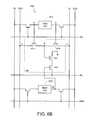
- FIG. 2is a block diagram of a CAM device within which CAM cells of present embodiments may be implemented.
- CAM device 200includes a CAM array 210 , an address decoder 220 , a comparand register 230 , a read/write circuit 240 , a priority encoder circuit 250 , and match logic 260 .
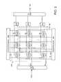
- CAM array 210includes any number of rows of CAM cells (not shown for simplicity in FIG. 2 ), where each row of CAM cells can be configured to store a data word. Further, while CAM array 210 is shown in FIG. 2 as a single CAM array, it may include any number of CAM array blocks that can be independently searched.
- One or more instructions and related control signalsmay be provided to CAM device 200 from an instruction decoder (not shown for simplicity) to control read, write, compare, and other operations for CAM device 200 .
- Other well-known signals that can be provided to CAM device 200such as enable signals, clock signals, and power connections, are not shown for simplicity.
- each row of CAM cells in CAM array 210may have one or more validity bits to indicate whether the corresponding row (or any segment thereof) of CAM cells stores valid data.
- Each row of CAM cells (not shown in FIG. 2 for simplicity) in CAM array 210is coupled to address decoder 220 via a corresponding word line WL, and to match latches 212 , to priority encoder 250 , and to well-known match logic 260 via a corresponding match line ML.
- the word lines and match linesare represented collectively in FIG. 2 .
- Address decoder 220is well-known, and includes circuitry to select corresponding rows in CAM array 210 for read, write, and/or other operations in response to an address received from an address bus ABUS using the word lines WL.
- addressesmay be provided to address decoder 220 from another suitable bus and/or circuitry.
- the match lines MLprovide match results for compare operations between comparand data (e.g., a search key) and data stored in CAM array 210 .
- Priority encoder 250uses the match results indicated on the match lines and latched in the match latches 212 to determine the matching entry that has the highest priority number associated with it and generates the index or address of this highest priority match (HPM).
- priority encoder 250may use the validity bits from CAM array 210 to generate the next free address that is available in CAM array 210 for storing new data.
- priority encoder 250may provide the next free address to the address decoder 220 .
- Match logic 260uses the match results indicated on the match lines to generate a match flag (MF) indicative of a match condition in CAM array 210 . If there is more than one matching entry in CAM array 210 , match logic 260 may generate a multiple match flag MF to indicate a multiple match condition. In addition, match logic 260 may use the validity bits from CAM array 210 to assert a full flag when all of the rows of CAM cells in CAM array 210 are filled with valid entries.
- MFmatch flag
- Each column of CAM cells (not shown in FIG. 2 for simplicity) in CAM array 210is coupled to comparand register 230 via one or more corresponding comparand lines CL, and is coupled to read/write circuit 240 via one or more corresponding bit lines BL.
- the comparand lines CL and bit lines BLare represented collectively in FIG. 2 .
- Comparand register 230is well-known, and is configured to provide a search key (e.g., a comparand word) received from a comparand bus CBUS to CAM array 210 during compare operations with data stored therein.
- the search keycan be provided to CAM array 210 via another bus and/or circuit.
- Read/write circuit 240includes well-known write drivers to write data received from a data bus DBUS to CAM array 210 via the bit lines BL, and includes well-known sense amplifiers to read data from CAM array 210 onto DBUS.
- read/write circuit 240may be coupled to a bus other than DBUS.
- CAM device 200can include a well-known global mask circuit (e.g., coupled to the comparand register 230 ) that can selectively mask the bits of the search key provided to the CAM array 210 .
- FIG. 3is a more detailed block diagram of the CAM array 210 of FIG. 2 .
- CAM array 210is shown to include a plurality of CAM cells 202 organized in any number of rows and columns.
- the CAM cells 202can be any suitable type of CAM cell including, for example, binary CAM cells, ternary CAM cells, and/or quaternary CAM cells.
- each row of CAM array 210may also include one or more validity bits.
- Each row of CAM cells 202is coupled to a match line ML and to a word line WL.
- Each word line WLis driven by address decoder 220 (see also FIG. 2 ) to select one or more rows of CAM cells 202 for writing or reading.
- Each match line MLis coupled to priority encoder 250 via a corresponding match latch 212 , which together form the match latches 212 of FIG. 2 .
- the match latches 212are clocked by a match latch clock signal CLK_ML in a well-known manner.
- Each column of CAM cells 202 in CAM array 210is coupled to read/write circuit 240 via a complementary bit line pair BL/BLB, and to comparand register 230 via a complementary comparand line pair CL/CLB.
- the match lines MLPrior to compare operations, the match lines ML are pre-charged (e.g., to logic high), and each set of complementary comparand line pairs CL/CLB are driven to the same predetermined logic level (e.g., to logic high). Then, during compare operations, the comparand register 230 provides the search key (e.g., the comparand word) to the CAM cells 202 by driving each pair of complementary comparand lines CL/CLB to opposite logic states indicative of the corresponding bit of the search key.
- the search keye.g., the comparand word
- the corresponding comparand line CLis driven to a first logic state (e.g., logic low) and the corresponding complementary comparand line CLB is driven to a second logic state (e.g., logic high); conversely, to provide a logic high comparand bit C to the column of CAM cells, the corresponding comparand line CL is driven to the second logic state (e.g., logic high) and the corresponding complementary comparand line CLB is driven to the first logic state (e.g., logic low).
- the match line MLremains in its logic high state to indicate the match condition.
- mismatching CAM cells 202discharge the match line ML (e.g., toward ground potential) to indicate the mismatch condition.
- FIG. 4shows a quaternary (XY) CAM cell 400 in accordance with the present embodiments.
- the XY CAM cell 400includes two memory cells 410 x and 410 y coupled to a compare circuit 420 .
- the memory cells 410 x and 410 ycan be any suitable type of storage cell including, for example, an SRAM cell, a DRAM cell, an EEPROM cell, a flash memory cell, a latch, or a register.
- memory cells 410are formed using cross-coupled CMOS inverter circuits, as known in the art.
- the first memory cell 410 xstores a first data bit “X”
- the second memory cell 410 ystores a second data bit “Y”.
- the two data bits X and Ycan collectively represent a data value D having four possible states: “0”, “1”, “don't care”, and a fourth state which may be left unused or may indicate “invalid,” as depicted in the truth table 150 of FIG. 1B .
- the logic “0” and “1” statescorrespond to the logic states represented by a conventional binary CAM cell.
- the compare circuit 420For each of these states, if the comparand data (e.g., provided to CAM cell 400 via complementary comparand lines CL and CLB) matches the data stored in CAM cell 400 , the compare circuit 420 does not discharge the match line ML, which remains in its charged state to indicate a match condition. Conversely, if the comparand data does not match the data stored in CAM cell 400 , compare circuit 420 discharges ML (e.g., toward ground potential) to indicate the mismatch condition.
- MLe.g., toward ground potential
- the logic low values for X and Ycause compare circuit 420 to remain in a non-conductive state, thereby preventing the match line from discharging. In this manner, the data value D stored in CAM cell 400 is masked from the compare operation, thereby forcing a match condition for CAM cell 400 , regardless of the comparand data.
- the logic high values for X and Ycause the compare circuit 420 to remain in a conductive state to discharge the match line to indicate a mismatch condition, irrespective of the comparand data.
- the “invalid” statecan be used to disable a row of CAM array 210 containing one or more XY CAM cells 400 , for example, as described in commonly-owned U.S. Pat. No. 6,865,098, which is incorporated by reference herein in its entirety.
- the compare circuit 420includes two match line pull-down transistors 421 x and 421 y , two pass transistors 422 x and 422 y , and two gating transistors 423 x and 423 y .
- a first group of transistors 421 x , 422 x , and 423 xforms a first selective pull-down circuit 425 x that selectively discharges the match line ML in response to a comparison of the complemented comparand bit ( C ) provided on CLB and the first data bit (X), and a second group of transistors 421 y , 422 y , and 423 y forms a second selective pull-down circuit 425 y that selectively discharges the match line ML in response to a comparison of the comparand bit (C) provided on CL and the second data bit (Y).
- the NMOS match line pull-down transistor 421 xis coupled between the match line ML and ground potential, and has a gate tied to a first node (Nx) that, in turn, is selectively coupled to receive X from the first memory cell 410 x via the PMOS pass transistor 422 x .
- the NMOS gating transistor 423 xis coupled between the gate of match line pull-down transistor 421 x and ground potential.
- the common gates of transistors 422 x and 423 xare coupled to the complementary comparand line CLB, and receive the complemented comparand bit ( C ) during compare operations.
- the NMOS match line pull-down transistor 421 yis coupled between the match line ML and ground potential, and has a gate tied to a second node (Ny) that, in turn, is selectively coupled to receive Y from the second memory cell 410 y via the PMOS pass transistor 422 y .
- the NMOS gating transistor 423 yis coupled between the gate of match line pull-down transistor 421 y and ground potential.
- the common gates of transistors 422 y and 423 yare coupled to the comparand line CL, and receive the comparand bit (C) during compare operations.
- the first node Nxcan be coupled to receive the complemented first data bit X
- the second node Nycan be coupled to receive the complemented second data bit Y
- the common gates of transistors 422 x and 423 xcan receive the comparand bit C
- the common gates of transistors 422 y and 423 ycan receive the complemented comparand bit C .
- the match line MLis pre-charged to logic high (e.g., towards VDD) by a suitable pre-charge circuit (not shown for simplicity), and the comparand lines CL/CLB are both pre-charged to logic high (e.g., towards VDD).
- the logic high state of CLBturns on NMOS transistor 423 x and turns off PMOS transistor 422 x .
- the conductive state of transistor 423 xpulls the gate of match line pull-down transistor 421 x (e.g., at node Nx) low towards ground potential, thereby maintaining transistor 421 x in a non-conductive state to isolate the match line ML from ground potential.
- the non-conductive state of transistor 422 xisolates the first memory cell 410 x from node Nx, thereby preventing the value of X from being pulled low to ground potential by the conductive NMOS transistor 423 x .
- the logic high state of CLturns on NMOS transistor 423 y and turns off PMOS transistor 422 y .
- the conductive state of transistor 423 ypulls the gate of match line pull-down transistor 421 y (e.g., at node Ny) low towards ground potential, thereby maintaining transistor 421 y in a non-conductive state to isolate the match line ML from ground potential.
- the non-conductive state of transistor 422 yisolates the second memory cell 410 y from node Ny, thereby preventing the value of Y from being pulled low to ground potential by the conductive NMOS transistor 423 y.
- the comparand bit Cis provided in a complementary manner to the XY CAM cell 400 via comparand lines CL and CLB. If a comparand line is driven to logic high, then the corresponding selective pull-down circuit 425 is disabled and does not discharge the match line ML. Conversely, if a comparand line is driven to logic low, then the corresponding selective pull-down circuit 425 is enabled and selectively discharges the match line ML in response to the corresponding data bit provided by the associated memory cell 410 .
- both selective pull-down circuits 425 x and 425 yare disabled and together prevent the match line ML from discharging, thereby causing the CAM cell 400 to indicate a match condition on ML irrespective of the data value D.
- CLis driven to logic high
- CLBis driven to logic low.
- the logic high state of CLdisables the second selective pull-down circuit 425 y (in the manner described above), and prevents the second data bit Y stored in second memory cell 410 y from affecting the compare operation.
- the logic low state of CLBenables the first selective pull-down circuit 425 x (in the manner described above), and allows the first data bit X stored in first memory cell 410 x to selectively discharge the match line ML.
- CLis driven to logic low
- CLBis driven to logic high.
- the logic low state of CLenables selective pull-down circuit 425 y (in the manner described above), and allows the second data bit Y stored in second memory cell 410 y to selectively discharge the match line ML.
- the compare circuit 420 of XY CAM cell 400includes only one transistor (e.g., transistor 421 ) in each pull-down path between the match line ML and ground potential, as shown in FIG. 4 .
- the conventional XY CAM cell 100 of FIG. 1Aincludes two series-connected transistors (e.g., transistors 131 - 132 and 133 - 134 , respectively) in each pull-down path between the match line ML and ground potential.
- the XY CAM cell 400 of present embodimentsis faster than the conventional XY CAM cell 100 of FIG. 1A .
- the compare circuit 420employs single stack pull-down elements (e.g., transistor 421 ) between the match line and ground potential
- the XY CAM cell 400puts less pull-down resistance and less capacitive loading on the match line than the 2-stack pull-down elements (e.g., transistors 131 - 132 and 133 - 134 , respectively) employed in the conventional XY CAM cell 100 , and therefore is faster than conventional XY CAM cell 100 .
- a CAM arraysuch as CAM array 210 of FIG. 2 can employ more CAM cells 400 in each row without degrading performance, as compared to conventional CAM cells 100 .
- the reduced match line capacitance resulting from fewer pull-down transistors in the compare stack of CAM cell 400may reduce power consumption, as compared with conventional XY CAM cells 100 of FIG. 1A .
- FIG. 5shows an XY CAM cell 500 in accordance with other embodiments.
- the XY CAM cell 500is modified to include a second compare circuit 520 that allows CAM cell 500 to perform two compare operations with the data value D stored therein at the same time, or alternatively in a sequential (e.g., staggered) manner.
- the XY CAM cell 500can simultaneously compare the data value D with a first comparand bit (C 1 ) provided on a first pair of complementary comparand lines CL 1 /CL 1 B and with a second comparand bit (C 2 ) provided on a second pair of complementary comparand lines CL 2 /CL 2 B, where the first pair of complementary comparand lines CL 1 /CL 1 B provide the first comparand bit C 1 and its complement C 1 to the first compare circuit 420 , and the second pair of complementary comparand lines CL 2 /CL 2 B provide the second comparand bit C 2 and its complement C 2 to the second compare circuit 520 .
- Match conditions between the data value D and the first comparand bit C 1are provided on a first match line ML 1 by the first compare circuit 420
- match conditions between the data value D and the second comparand bit C 2are provided on a second match line ML 2 by the second compare circuit 520 .
- the second compare circuit 520includes two match line pull-down transistors 521 x and 521 y , two pass transistors 522 x and 522 y , and two gating transistors 523 x and 523 y .
- a first group of transistors 521 x , 522 x , and 523 xforms a first selective pull-down circuit 525 x that selectively discharges the second match line ML 2 in response to a comparison with the complemented second comparand bit ( C 2 ) and the first data bit (X)
- a second group of transistors 521 y , 522 y , and 523 yforms a second selective pull-down circuit 525 y that selectively discharges the second match line ML 2 in response to a comparison with the second comparand bit (C 2 ) and the second data bit (Y).
- the NMOS match line pull-down transistor 521 xis coupled between the second match line ML 2 and ground potential, and has a gate tied to a third node (Mx) that, in turn, is selectively coupled to receive X from the first memory cell 410 x via the PMOS pass transistor 522 x .
- the NMOS gating transistor 523 xis coupled between the gate of match line pull-down transistor 521 x and ground potential.
- the common gates of transistors 522 x and 523 xare coupled to the second complementary comparand line CL 2 B, and receive the complemented second comparand bit ( C 2 ) during compare operations.
- the NMOS match line pull-down transistor 521 yis coupled between the second match line ML 2 and ground potential, and has a gate tied to a fourth node (My) that, in turn, is selectively coupled to receive Y from the second memory cell 410 y via the PMOS pass transistor 522 y .
- the NMOS gating transistor 523 yis coupled between the gate of match line pull-down transistor 521 y and ground potential.
- the common gates of transistors 522 y and 523 yare coupled to the second comparand line CL 2 , and receive the second comparand bit (C 2 ) during compare operations.
- Compare operations for XY CAM cell 500are performed in a manner similar to that described above with respect to CAM cell 400 of FIG. 4 , except that XY CAM cell 500 can perform two compare operations at the same time (or alternately in a sequential or staggered manner).
- the first and second match lines ML 1 and ML 2are both pre-charged to logic high (e.g., towards VDD) by suitable pre-charge circuits (not shown for simplicity), and both sets of complementary comparand lines CL 1 /CL 1 B and CL 2 /CL 2 B are pre-charged to logic high (e.g., towards VDD).
- the first compare circuit 420isolates the first match line ML 1 from ground potential
- the second compare circuit 520isolates the second match line ML 2 from ground potential.
- the first comparand bit C 1is provided to the XY CAM cell 500 in a complementary manner via comparand lines CL 1 and CL 1 B
- the second comparand bit C 2is provided to the XY CAM cell 500 in a complementary manner via comparand lines CL 2 and CL 2 B. If a comparand line is driven to logic high, then the corresponding selective pull-down circuit 425 / 525 is disabled and does not discharge its associated match line ML. Conversely, if a comparand line is driven to logic low, then the corresponding selective pull-down circuit 425 / 525 is enabled and selectively discharges its associated match line ML in response to the corresponding data bit provided by the associated memory cell 410 .
- both selective pull-down circuits 425 x and 425 yare disabled and together prevent the first match line ML 1 from discharging, thereby causing the CAM cell 500 to indicate a match condition on ML 1 irrespective of the data value D.
- both CL 2 and CL 2 Bare driven to logic high (e.g., to achieve a column-masking function)
- both selective pull-down circuits 525 x and 525 yare disabled and together prevent the second match line ML 2 from discharging, thereby causing the CAM cell 500 to indicate a match condition on ML 2 irrespective of the data value D.
- the second compare circuit 520 of XY CAM cell 500includes only one transistor (e.g., transistor 521 ) in each pull-down path between the second match line ML 2 and ground potential, as shown in FIG. 5 .
- the conventional XY CAM cell 100 of FIG. 1Aincludes two series-connected transistors (e.g., transistors 131 - 132 and 133 - 134 , respectively) in each pull-down path between the match line ML and ground potential.
- the XY CAM cell 500 of present embodimentsis faster than the conventional XY CAM cell 100 of FIG. 1A .
- the compare circuit 520employs single stack pull-down elements (e.g., transistor 521 ) between the second match line ML 2 and ground potential, the compare circuit 520 puts less pull-down resistance and less capacitive loading on the match line than the 2-stack pull-down elements (e.g., transistors 131 - 132 and 133 - 134 , respectively) employed in the conventional XY CAM cell 100 , and therefore is faster and may even consume less power than conventional XY CAM cell 100 . Further, because each CAM cell 500 puts less capacitive loading on each of the match lines ML 1 and ML 2 , a CAM array such as CAM array of FIG. 2 can employ more CAM cells 500 in each row without degrading performance, as compared to conventional CAM cells 100 .
- the 2-stack pull-down elementse.g., transistors 131 - 132 and 133 - 134 , respectively
- FIG. 6Ais a block diagram of a ternary content addressable memory (TCAM) cell 601 with a data cell 610 , a mask cell 620 , and a compare circuit 630 .
- the compare circuit 630includes pull-down transistor pairs 631 A- 631 B and 632 A- 632 B, and is configured to receive complementary (also known as “differential” or “balanced”) input signals.
- the pull-down transistors 631 A and 631 Bare controlled by complementary data signals D and D , respectively, provided by the data cell 610
- the pull-down transistors 632 A and 632 Bare controlled by complementary comparand bits C and C, respectively.
- compare circuit 630The symmetrical structure and operation of compare circuit 630 is advantageous because it provides balanced impedances and mutually cancelled noises.
- the discharge path between the match line ML and ground potential for the CAM cell 601includes 3 series-connected pull-down transistors 631 , 632 , and 633 , which in turn results in slower performance than TCAM cells that have fewer transistors in their compare stack.
- FIG. 6Bis a block diagram of another TCAM cell 602 having data cell 610 , mask cell 620 , and a compare circuit 640 .
- the compare circuit 640includes pass transistors 641 A and 641 B, and includes pull-down transistors 642 and 643 .
- Transistor 641 Ais coupled between complementary comparand line CLB and a node N
- transistor 641 Bis coupled between the node N and comparand line CL.
- the gates of pass transistors 641 A and 641 Breceive complementary data bits D and D , respectively, from the data cell 610 .
- Pull-down transistors 642 and 643are connected in series between match line ML and ground potential, with the gate of transistor 642 coupled to node N, and with the gate of transistor 643 coupled to receive a complemented mask bit from the mask cell 620 .
- the CAM cell 602has fewer transistors than the CAM cell 601 of FIG. 6A , and the compare circuit 640 has only 2 transistors connected in series between the match line ML and ground potential. As a result, the capacitance on match line ML is also smaller as compared to the CAM cell 601 .
- the current and time associated with driving the complementary comparand lines CL and CLBmay be significantly higher for CAM cell 602 than for CAM cell 601 . For example, because pass transistors 641 A and 641 B are controlled by complementary data bits D and D , respectively, one of the pass transistors 641 A and 641 B may undesirably turn on during the pre-charge phase.
- the charging circuitry(not shown) for CL and CLB drives not only the capacitance of the comparand lines, but also the source/drain capacitance of one of the pass transistors 641 , the gate capacitance seen by the node N, and any associated parasitic capacitances. These extra capacitances adversely affect the performance and the scalability of the CAM cell 602 .
- FIG. 6Cis a block diagram of a TCAM cell 603 that incorporates an XY bit encoding technique.
- TCAM cell 603is structurally similar to the quaternary CAM cell 100 of FIG. 1A , except that TCAM cell 603 has only three possible states: “0”, “1”, and “don't care,” as depicted in the truth table of FIG. 6D . More specifically, TCAM cell 603 is shown to include data cell 610 , mask cell 620 , and a compare circuit 650 .
- the compare circuit 650includes a first ML discharge path formed by pull-down transistors 651 and 652 A, and includes a second ML discharge path formed by pull-down transistors 653 and 652 B.
- the gate of transistor 651receives a “data” bit (X) from data cell 610
- the gate of transistor 653receives a “mask” bit (Y) from mask cell 620
- the gate of transistor 652 Areceives the comparand bit C from the comparand line CL
- the gate of transistor 652 Breceives the complementary comparand bit C from the complementary comparand line CLB.
- the compare circuit 650 of CAM cell 603is a 2-stack compare circuit.
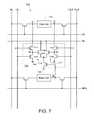
- FIG. 7shows a block diagram of a TCAM cell 700 in accordance with some embodiments.
- TCAM cell 700includes a data cell 710 , a mask cell 720 , and a compare circuit 730 .
- Both data cell 710 and mask cell 720can be implemented with any suitable type of storage cell including, for example, an SRAM cell, DRAM cell, Flash memory cell, STT cell, and so on.
- the TCAM cell 700can store three possible states: “0”, “1”, or “don't care.” Thus, when TCAM cell 700 stores a “0” or a “1,” TCAM cell 700 operates in a manner similar to binary CAM cells.
- compare circuit 730does not discharge the match line ML, which remains in its pre-charged state to indicate the match condition. Conversely, if the comparand bit C does not match the data bit D, then compare circuit 730 discharges the match line ML (e.g., toward ground potential) to indicate the mismatch condition.
- an active mask bitis stored in mask cell 720 to prevent compare circuit 730 from discharging the match line ML, regardless of the values of D and C.
- compare circuit 730includes two NMOS match line pull-down transistors 733 A and 733 B, two PMOS pass transistors 731 A and 731 B, two NMOS gating transistors 732 A and 732 B, and an NMOS mask discharge transistor 735 .
- the mask transistor 735is controlled by the mask cell 720 .
- a first group of transistors 731 A, 732 A, and 733 Aforms a first selective pull-down circuit 740 A that selectively discharges the match line ML in response to a comparison between the comparand bit C provided on CL and the data bit D stored in the data cell 710
- a second group of transistors 731 B, 732 B, and 733 Bforms a second selective pull-down circuit 740 B that selectively discharges the match line ML in response to a comparison between the complemented comparand bit C provided on CLB and the complemented data bit D .
- the NMOS match line pull-down transistor 733 Ais coupled between the match line ML and the discharge transistor 735 , and has a gate tied to a first node (Na) that selectively receives the data bit D via PMOS pass transistor 731 A in response to the comparand bit C.
- the gate of match line pull-down transistor 733 Ais selectively driven by D in response to C.
- the NMOS gating transistor 732 Ais coupled between the gate of match line pull-down transistor 733 A (e.g., node Na) and ground potential.
- the common gates of transistors 731 A and 732 Aare coupled to the comparand line CL, and receive the comparand bit C during compare operations.
- the NMOS match line pull-down transistor 733 Bis coupled between the match line and the discharge transistor 735 , and has a gate tied to a second node (Nb) that selectively receives D via the PMOS pass transistor 731 B in response to C .
- Nbsecond node
- the gate of match line pull-down transistor 733 Bis selectively driven by D in response to C .
- the NMOS gating transistor 732 Bis coupled between the gate of match line pull-down transistor 733 B (e.g., node Nb) and ground potential.
- the common gates of transistors 731 B and 732 Bare coupled to the complementary comparand line CLB, and receive the complemented comparand bit C during compare operations.
- the NMOS mask discharge transistor 735is coupled between the common sources of transistors 733 A- 733 B and ground potential, and has a gate coupled to one side of the mask cell 720 (e.g., to the side that provides the complement of the value of the mask bit stored in the mask cell).
- each discharge path in compare circuit 730has only two series-connected transistors, as in the case of CAM cell 602 of FIG. 6B and CAM cell 603 of FIG. 6C .
- the complementary data bits (D and D ) and the complementary comparand bits (C and C )are provided to and processed by compare circuit 730 in a differential manner, which can improve performance over CAM cells 602 and 603 by providing balanced impedances. Therefore, in accordance with present embodiments, the TCAM cell 700 in FIG. 7 incorporates the advantages of differential compare circuitry and a shortened, two-transistor pull-down stack.
- the match line MLis pre-charged to logic high (e.g., towards VDD) by a suitable pre-charge circuit (not shown for simplicity), and the comparand lines CL/CLB are both pre-charged to logic high (e.g., towards VDD).
- the logic high state of CLturns on NMOS transistor 732 A and turns off PMOS transistor 731 A.
- the conductive state of transistor 732 Apulls the gate of match line pull-down transistor 733 A (e.g., at node Na) low towards ground potential, thereby maintaining transistor 733 A in a non-conductive state to isolate the match line ML from ground potential.
- the non-conductive state of transistor 731 Aisolates the data cell 710 from node Na, thereby preventing the value of D from being pulled low to ground potential by the conductive NMOS transistor 732 A.
- the logic high state of CLBturns on NMOS transistor 732 B and turns off PMOS transistor 731 B.
- the conductive state of transistor 732 Bpulls the gate of match line pull-down transistor 733 B (e.g., at node Nb) low towards ground potential, thereby maintaining transistor 733 B in a non-conductive state to isolate the match line ML from ground potential.
- the non-conductive state of transistor 731 Bisolates the data cell 710 from node Nb, thereby preventing the value of D from being pulled low towards ground potential by the conductive NMOS transistor 732 B.
- the comparand bit Cis provided in a complementary manner to the TCAM cell 700 via comparand lines CL and CLB.
- the corresponding selective pull-down circuit 740is enabled and selectively discharges the match line ML in response to the corresponding data bit D and the comparand bit C.
- the logic low state of CLturns off NMOS transistor 732 A and turns on PMOS transistor 731 A, thereby allowing the logic state of D to propagate through transistor 731 A to node Na and selectively turn on match line pull-down transistor 733 A, thereby selectively discharging the match line ML in response to the logic state of D.
- both selective pull-down circuits 740 A and 740 Bare disabled and together prevent the match line ML from discharging, thereby causing the CAM cell 700 to indicate a match condition on ML irrespective of the data value D.
- CLis driven to logic high
- CLBis driven to logic low.
- the logic high state of CLdisables the first selective pull-down circuit 740 A (in the manner described above), and prevents the data bit D from affecting the compare operation.
- the logic low state of CLBenables the second selective pull-down circuit 740 B, and allows the complemented data bit D stored in the data cell 710 to selectively discharge the match line ML via match line pull-down transistor 733 B.
- the logic low value of Dpropagates through pass gate transistor 731 B to node Nb.
- the compare circuit 730 of TCAM cell 700includes only two transistors (e.g., transistors 733 and 735 ) in each pull-down path between the match line and ground potential, as shown in FIG. 7 .
- the TCAM cell 601 of FIG. 6Aincludes three series-connected transistors (e.g., transistors 631 , 632 , and 633 ) in each pull-down path between the match line and ground potential.
- the TCAM cell 700 of present embodimentsis faster than the TCAM cell 601 of FIG. 6A .
- the compare circuit 730employs double stack pull-down elements (e.g., transistors 733 and 735 ) between the match line and ground potential
- the TCAM cell 700puts less pull-down resistance and less capacitive loading on the match line than the 3-stack pull-down elements (e.g., transistors 631 , 632 , and 633 ) employed in the TCAM cell 601 , and therefore is faster than TCAM cell 601 .
- a CAM arraysuch as CAM array 210 of FIG. 2 can employ more CAM cells 700 in each row without degrading performance, as compared to CAM cells 601 .
- the reduced match line capacitance resulting from fewer pull-down transistors in the compare stack of CAM cell 700may reduce power consumption, as compared with TCAM cells 601 of FIG. 6A .
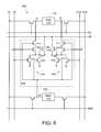
- FIG. 8is a block diagram of a TCAM cell 800 in accordance with other embodiments.
- TCAM cell 800includes data cell 710 , mask cell 720 , and a compare circuit 830 .
- the complementary data bits (D and D ) stored in data cell 710are applied to compare circuit 830 in a differential manner.
- TCAM cell 800when TCAM cell 800 stores a “0” or a “1,” TCAM cell 800 operates in a manner similar to binary CAM cells. For example, during compare operations, if the comparand bit C matches the data bit D stored in data cell 710 , then compare circuit 830 does not discharge the match line ML, which remains in its pre-charged state to indicate the match condition. Conversely, if the comparand bit C does not match the data bit D, then compare circuit 830 discharges the match line ML (e.g., toward ground potential) to indicate the mismatch condition.
- the match line MLe.g., toward ground potential
- the compare circuit 830includes two NMOS match line pull-down transistors 835 A and 835 B, four PMOS pass transistors 831 A, 832 A, 831 B, and 832 B, and four NMOS gating transistors 833 A, 834 A, 833 B, and 834 B.
- a first group of transistors 831 A, 832 A, 833 A, 834 A, and 835 Aforms a first selective pull-down circuit 840 A that selectively discharges the match line ML in response to a comparison between the comparand bit C provided on CL and the data bit (D) stored in the data cell 710
- a second group of transistors 831 B, 832 B, 833 B, 834 B, and 835 Bforms a second selective pull-down circuit 840 B that selectively discharges the match line ML in response to a comparison between the complemented comparand bit ( C ) provided on CLB and the complemented data bit ( D ) stored in the data cell 710 .
- the mask cell 720can be configured to disable the compare circuit 830 and prevent the match line ML from discharging. In this manner, the data value D stored in data cell 710 is masked from the compare operation, thereby forcing a match condition for the CAM cell 800 , regardless of the comparand data.
- the NMOS match line pull-down transistor 835 Ais coupled between the match line ML and ground potential, and has a gate tied to a first node (Na) that selectively receives D from the data cell 710 via series-connected PMOS pass transistors 831 A and 832 A.
- NMOS gating transistors 833 A and 834 Aare connected in parallel between the gate of match line pull-down transistor 835 A (at node Na) and ground potential.
- the first pass transistor 832 A and the first gating transistor 833 Ahave gates coupled to the comparand line CL, and receive the comparand bit C during compare operations.
- the second pass transistor 831 A and the second gating transistor 834 Ahave gates coupled to the mask cell 720 and receive the mask bit M during compare operations.
- the gate of the first match line pull-down transistor 835 Ais responsive to a logical combination of the data bit D, the mask bit M, and the comparand bit C.
- the NMOS match line pull-down transistor 835 Bis coupled between the match line ML and ground potential, and has a gate tied to a second node (Nb) that selectively receives D from the data cell 710 via series-connected PMOS pass transistors 831 B and 832 B.
- NMOS gating transistors 833 B and 834 Bare connected in parallel between the gate of match line pull-down transistor 835 B (at node Nb) and ground potential.
- the third pass transistor 832 B and the third gating transistor 833 Bhave gates coupled to the complementary comparand line CLB, and receive the complemented comparand bit C during compare operations.
- the fourth pass transistor 831 B and the fourth gating transistor 834 Bhave gates coupled to the mask cell 720 and receive M during compare operations.
- the gate of the second match line pull-down transistor 835 Bis responsive to a logical combination of the complemented data bit D , the mask bit M, and the complemented comparand bit C .
- the TCAM cell 800 of FIG. 8incorporates both advantages of differential circuitry and a shortened, one-transistor pull-down path. Note that while CAM cell 700 in FIG. 7 has a lower overall transistor count in its compare circuit 730 , CAM cell 800 in FIG. 8 has a shorter, one-transistor pull-down path in its compare circuit 830 .
- the match line MLis pre-charged to logic high (e.g., towards VDD) by a suitable pre-charge circuit (not shown for simplicity), and the comparand lines CL/CLB are both pre-charged to logic high (e.g., towards VDD), which in turn disable corresponding selective pull-down circuits 840 A and 840 B.
- the logic high state of CLturns on NMOS transistor 833 A and turns off PMOS transistor 832 A.
- the conductive state of transistor 833 Apulls the gate of match line pull-down transistor 835 A (e.g., at node Na) low towards ground potential, thereby maintaining transistor 835 A in a non-conductive state to isolate the match line ML from ground potential.
- the non-conductive state of transistor 832 Aisolates the data cell 710 from node Na, thereby preventing the value of D from being pulled low to ground potential by the conductive NMOS transistor 833 A.
- the logic high state of CLBturns on NMOS transistor 833 B and turns off PMOS transistor 832 B.
- the conductive state of transistor 833 Bpulls the gate of match line pull-down transistor 835 B (e.g., at node Nb) low towards ground potential, thereby maintaining transistor 835 B in a non-conductive state to isolate the match line ML from ground potential.
- the non-conductive state of transistor 832 Bisolates the data cell 710 from node Nb, thereby preventing the value of D from being pulled low to ground potential by the conductive NMOS transistor 833 B.
- the comparand bit Cis provided in a complementary manner to the TCAM cell 800 via comparand lines CL and CLB.
- both selective pull-down circuits 840 A and 840 Bare disabled and together prevent the match line ML from discharging, thereby causing the CAM cell 800 to indicate a match condition on ML irrespective of the data value D.
- CLis driven to logic high
- CLBis driven to logic low.
- the logic high state of CLdisables the first selective pull-down circuit 840 A (in the manner described above), and prevents the data bit D from affecting the compare operation.
- the logic low state of CLBenables the second selective pull-down circuit 840 A, thereby allowing the complemented data bit D to selectively discharge the match line ML. More specifically, the logic low state of CLB turns on PMOS transistor 832 B and turns off NMOS transistor 833 B.
- transistor 832 Ballows D to propagate to second node Nb, and the non-conductive state of transistor 833 B isolates node Nb from the ground potential.
- the logic low value of Dpropagates through pass gate transistors 831 B and 832 B to node Nb.
- the compare circuit 830 of TCAM cell 800includes only one transistor (e.g., transistor 835 ) in each pull-down path between the match line and ground potential, as shown in FIG. 8 .
- the TCAM cell 601 of FIG. 6Aincludes three series-connected transistors (e.g., transistors 631 - 632 - 633 ) in each pull-down path between the match line and ground potential, and the TCAM cells 602 and 603 of FIG. 6B and FIG. 6C , respectively, each include two series-connected transistors (e.g., transistors 642 - 643 in FIG. 6B , and transistors 651 - 652 A or transistors 653 - 652 B in FIG.
- the TCAM cell 800 of FIG. 8is faster than the TCAM cell 601 - 603 . More specifically, because the compare circuit 830 employs single stack pull-down elements (e.g., transistor 835 ) between the match line and ground potential, the TCAM cell 800 puts less pull-down resistance and less capacitive loading on the match line than the 3-stack or 2-stack pull-down elements employed in other TCAM cells, and therefore is faster than such other TCAM cells. Further, because each CAM cell 800 puts less capacitive loading on the match line, a CAM array such as CAM array 210 of FIG.
- a CAM arraysuch as CAM array 210 of FIG.
- the reduced match line capacitance resulting from fewer pull-down transistors in the compare stack of CAM cell 800may reduce power consumption, as compared with TCAM cells 601 - 603 .
- FIG. 9Ais a block diagram of a TCAM cell 900 that incorporates an XY encoding technique in accordance with some embodiments.
- TCAM cell 900includes a data cell 710 , a mask cell 720 , and a compare circuit 930 .
- the data stored in the data cell 710is applied to a compare circuit 930 in a differential manner as D and D .
- the mask bit stored in the mask cell 720is also applied to the compare circuit 930 in a differential manner as M and M .
- the mask cell 720can be configured, together with the data cell 710 , to disable the compare circuit 930 from discharging a match line ML, leaving the match line ML always logic high.
- the TCAM cell 900can be configured to store three possible states: “0”, “1”, or “don't care,” as depicted in the truth table 950 of FIG. 9B .
- the TCAM cell 900stores a “0” or a “1”
- the TCAM cell 900operates as a binary CAM cell.
- the mask cell 720 and the data cell 710store the same logic value (e.g., both “0” or both “1)
- the TCAM cell 900stores a “don't care” value and indicates a match condition regardless of the comparand data applied to the TCAM cell.
- the compare circuit 930includes a single match line pull-down transistor 934 , two pass transistors 931 A and 931 B, two gating transistors 932 A and 932 B, and two control transistors 933 A and 933 B.
- a first group of transistors 931 A, 932 A, and 933 Aforms a first selective pull-down control circuit 940 A that controls the match line pull-down transistor 934 and selectively discharges the match line ML in response to a comparison between the complemented comparand bit ( C ) provided on CLB, the data bit (D) stored in the data cell 710 , and the mask bit (M) stored in the mask cell 720 .
- a second group of transistors 931 B, 932 B, and 933 Bforms a second selective pull-down control circuit 940 B that controls the match line pull-down transistor 934 and selectively discharges the match line ML in response to a comparison between the comparand bit (C) provided on CL, the complemented data bit ( D ) stored in the data cell 710 , and the complemented mask bit ( M ) stored in the data cell 720 .
- the mask cell 720 and the data cell 710can together be configured to disable the compare circuit 930 and prevent the match line ML from discharging. In this manner, the data value stored in CAM cell 900 is masked from the compare operation, thereby forcing a match condition for the CAM cell 900 , regardless of the comparand data.
- the NMOS match line pull-down transistor 934is coupled between the match line ML and ground potential, and has a gate tied to a pull-down or discharge node (Np) that selectively receives control signals from match line pull-down control circuits 940 A and 940 B.
- the PMOS control transistor 933 Ais coupled between the pull-down node Np and a first node (Na), and has a gate to receive the mask bit M from mask cell 720 .
- the NMOS gating transistor 932 Ais coupled between ground potential and the first node Na, which in turn selectively receives D from data cell 710 via PMOS pass transistor 931 A.
- PMOS pass transistor 931 A and NMOS gating transistor 932 Aare connected in series, and have gates coupled to the complementary comparand line CLB.
- PMOS control transistor 933 Bis coupled between the pull-down node Np and a second node (Nb), and has a gate to receive the complemented mask bit M from mask cell 720 .
- the NMOS gating transistor 932 Bis coupled between ground potential and the second node Nb, which in turn selectively receives D from data cell 710 via PMOS pass transistor 931 B.
- PMOS pass transistor 931 B and NMOS gating transistor 932 Bare connected in series, and have gates coupled to the complementary comparand line CL.
- the gate of the single match line pull-down transistor 934is responsive to (1) a logical combination of the data bit D, the mask bit M, and the complemented comparand bit C , and (2) a logical combination of the complemented data bit D , the complemented mask bit M , and the comparand bit C.
- TCAM cell 900 of FIG. 9Aincorporates both advantages of differential compare circuitry and a shortened, one-transistor pull-down path. It is further observed that the CAM cell 900 in FIG. 9A has the same, reduced overall transistor count in its compare circuit 930 as the compare circuit 730 of CAM cell 700 in FIG. 7 .
- PMOS control transistors 933 A and 933 Bcan be NMOS transistors, in which case the gate of transistor 933 A receives M and the gate of transistor 933 B receives M.
- a compare operation between a comparand bit C and a data value (represented by the data bit D and the mask bit M, as illustrated in FIG. 9B ) stored in the CAM cell 900is now described.
- the match line MLis pre-charged to logic high (e.g., towards VDD) by a suitable pre-charge circuit (not shown for simplicity), and the comparand lines CL/CLB are both pre-charged to logic high (e.g., towards VDD).
- the logic high state of CLturns on NMOS transistor 932 B and turns off PMOS transistor 931 B, thereby pulling node Nb low to ground potential.
- transistor 933 Bmay be turned on because of the complementary mask bit M and M , in the case that 933 B is turned on, the conductive state of transistor 933 B pulls the gate of match line pull-down transistor 934 (e.g., at node Np) low towards ground potential, thereby maintaining transistor 934 in a non-conductive state to isolate the match line ML from ground potential.
- the non-conductive state of transistor 931 Bisolates the data cell 710 from node Nb, thereby preventing the value of D from being pulled low to ground potential by the conductive NMOS transistor 932 B.
- the logic high state of CLBturns on NMOS transistor 932 A and turns off PMOS transistor 931 A, thereby pulling node Na low to ground potential. Therefore, although one of the control transistors 933 A and 933 B may be turned on because of the complementary mask bit M and M , in the case that 933 A is turned on, the conductive state of transistor 933 A pulls the gate of match line pull-down transistor 934 (e.g., at node Np) low towards ground potential, thereby maintaining transistor 934 in a non-conductive state to isolate the match line ML from ground potential.
- the non-conductive state of transistor 931 Aisolates the data cell 710 from node Na, thereby preventing the value of D from being pulled low to ground potential by the conductive NMOS transistor 932 A.
- the comparand bit Cis provided in a complementary manner to the TCAM cell 900 via comparand lines CL and CLB.
- the mask cell 720 and the data cell 710store either a logic 0 or a logic 1 value.
- CLis driven to logic high
- CLBis driven to logic low.
- the logic high state of CLturns off pass transistor 931 B and turns on gating transistor 932 B of the second selective pull-down control circuit 940 B, thereby preventing the complemented data bit D from affecting the compare operation.
- the logic low state of CLBturns off gating transistor 932 A and turns on pass transistor 931 A of the first selective pull-down control circuit 940 A, thereby allowing the data bit D, the mask bit M, and the complemented mask bit M to selectively discharge the match line ML.
- the logic low value of Mturns on control transistor 933 B, which pulls the logic state of the pull-down node Np low to ground potential via gating transistor 932 B.
- the logic high state of Mturns off control transistor 933 A, and preserves the logic state of the data bit D.
- the logic high value of Dpropagates through pass transistor 931 A to node Na.
- the logic low value of Mturns on control transistor 933 A, so that the logic high value of D propagates to the pull-down node Np.
- the logic high state of Mturns off control transistor 933 B to prevent the pull-down node Np from being pulled low to ground potential by gating transistor 932 B.
- CLis driven to logic low
- CLBis driven to logic high. More specifically, the logic high state of CLB turns off pass transistor 931 A and turns on gating transistor 932 A of the first selective pull-down control
- the logic low value of Mturns on control transistor 933 A, and pulls the pull-down node Np low to ground potential via gating transistor 932 A.
- the logic high state of Mturns off control transistor 933 B, and preserves the logic state of the complemented data bit D .
- the logic high value of Dpropagates through pass gate transistor 931 B to the pull-down node Nb.
- the logic low value of Mturns on control transistor 933 B, so that the logic high value of D propagates to the pull-down node Np.
- the logic high state of Mturns off control transistor 933 A to prevent node Np from being pulled low to ground potential by gating transistor 932 A.
- the mask bit Mdisables the first selective pull-down control circuit 940 A by turning off control transistor 933 A
- the complemented mask bit Menables the second selective pull-down control circuit 940 B by turning on control transistor 933 B.
- pass transistor 931 Bturns off and gating transistor 932 B turns on, which in turn pulls the gate of the match line pull-down transistor 934 (e.g., at node Np) low to ground potential, thereby turning off pull-down transistor 934 and forcing a match condition.
- gating transistor 932 Bturns off and pass transistor 931 B turns on, which in turn allows the logic low state of D to pull the gate of the match line pull-down transistor 934 (e.g., at node Np) low to ground potential, thereby turning off pull-down transistor 934 and forcing a match condition.
- the mask bit Menables the first selective pull-down control circuit 940 A by turning on control transistor 933 A
- the complemented mask bit Mdisables the second selective pull-down control circuit 940 B by turning off control transistor 933 B. Therefore, if the complemented comparand bit C is logic high, pass transistor 931 A turns off and gating transistor 932 A turns on, which in turn pulls the gate of the match line pull-down transistor 934 (e.g., at node Np) low to ground potential, thereby turning off pull-down transistor 934 and forcing a match condition.
- the match line pull-down transistor 934e.g., at node Np
- CAM cell 900indicates a match regardless of the value of the comparand data applied when data cell 710 and mask cell 720 both store the same value.
- both selective pull-down control circuits 940 A and 940 Bare disabled and together prevent the match line ML from discharging by maintaining match line pull-down transistor 934 in a non-conductive state, thereby causing the CAM cell 900 to indicate a match condition on ML irrespective of the data value D.
- the compare circuit 930 of TCAM cell 900includes only one transistor (e.g., transistor 934 ) in the pull-down path between the match line and ground potential, as shown in FIG. 9A .
- the TCAM cell 601 of FIG. 6Aincludes three series-connected transistors (e.g., transistors 631 - 632 - 633 ) in each pull-down path between the match line and ground potential
- the TCAM cells 602 and 603 of FIG. 6B and FIG. 6Cinclude two series-connected transistors (e.g., transistors 642 - 643 in FIG. 6B , and transistors 651 - 652 A or transistors 653 - 652 B in FIG.
- the TCAM cell 900 of present embodimentsis faster than the TCAM cells 601 - 603 . More specifically, because the compare circuit 930 employs single stack pull-down elements (e.g., transistor 934 ) between the match line and ground potential, the TCAM cell 900 puts less pull-down resistance and less capacitive loading on the match line than the 3-stack or 2-stack pull-down elements employed in the TCAM cells 601 - 603 , and therefore is faster than TCAM cells 601 - 603 .
- the compare circuit 930employs single stack pull-down elements (e.g., transistor 934 ) between the match line and ground potential
- the TCAM cell 900puts less pull-down resistance and less capacitive loading on the match line than the 3-stack or 2-stack pull-down elements employed in the TCAM cells 601 - 603 , and therefore is faster than TCAM cells 601 - 603 .
- CAM cell 900advantageously includes only one pull-down path between match line ML and ground potential (e.g., through transistor 934 ), which also reduces match line capacitance compared to CAM cells (such as CAM cells 601 - 603 ) that each include two pull-down paths between the match line and ground potential. Further, because each CAM cell 900 puts less capacitive loading on the match line, a CAM array such as CAM array 210 of FIG. 2 can employ more CAM cells 900 in each row without degrading performance, as compared to CAM cells 601 - 603 . Further, the reduced match line capacitance resulting from fewer pull-down transistors in the compare stack of CAM cell 900 may reduce power consumption, as compared with TCAM cells 601 - 603 .
- circuits disclosed hereinmay be described using computer aided design tools and expressed (or represented), as data and/or instructions embodied in various non-transitory computer-readable media, in terms of their behavioral, register transfer, logic component, transistor, layout geometries, and/or other characteristics. Formats of files and other objects in which such circuit expressions may be implemented include, but are not limited to, formats supporting behavioral languages such as C, Verilog, and VHDL, formats supporting register level description languages like RTL, and formats supporting geometry description languages such as GDSII, GDSIII, GDSIV, CIF, MEBES and any other suitable formats and languages.
- Non-transitory computer-readable media in which such formatted data and/or instructions may be embodiedinclude, but are not limited to, non-volatile storage media in various forms (e.g., optical, magnetic or semiconductor storage media).
Landscapes
- Static Random-Access Memory (AREA)
Abstract
Description
Claims (21)
Priority Applications (1)
| Application Number | Priority Date | Filing Date | Title |
|---|---|---|---|
| US13/149,878US8582338B1 (en) | 2010-08-31 | 2011-05-31 | Ternary content addressable memory cell having single transistor pull-down stack |
Applications Claiming Priority (3)
| Application Number | Priority Date | Filing Date | Title |
|---|---|---|---|
| US37880810P | 2010-08-31 | 2010-08-31 | |
| US13/015,543US8462532B1 (en) | 2010-08-31 | 2011-01-27 | Fast quaternary content addressable memory cell |
| US13/149,878US8582338B1 (en) | 2010-08-31 | 2011-05-31 | Ternary content addressable memory cell having single transistor pull-down stack |
Related Parent Applications (1)
| Application Number | Title | Priority Date | Filing Date |
|---|---|---|---|
| US13/015,543Continuation-In-PartUS8462532B1 (en) | 2010-08-31 | 2011-01-27 | Fast quaternary content addressable memory cell |
Publications (1)
| Publication Number | Publication Date |
|---|---|
| US8582338B1true US8582338B1 (en) | 2013-11-12 |
Family
ID=49518076
Family Applications (1)
| Application Number | Title | Priority Date | Filing Date |
|---|---|---|---|
| US13/149,878Expired - Fee RelatedUS8582338B1 (en) | 2010-08-31 | 2011-05-31 | Ternary content addressable memory cell having single transistor pull-down stack |
Country Status (1)
| Country | Link |
|---|---|
| US (1) | US8582338B1 (en) |
Cited By (15)
| Publication number | Priority date | Publication date | Assignee | Title |
|---|---|---|---|---|
| US20130250642A1 (en)* | 2010-12-13 | 2013-09-26 | Broadcom Corporation | Low Power Content-Addressable Memory |
| US20140177310A1 (en)* | 2012-12-26 | 2014-06-26 | Qualcomm Incorporated | Pseudo-nor cell for ternary content addressable memory |
| US8773880B2 (en) | 2011-06-23 | 2014-07-08 | Netlogic Microsystems, Inc. | Content addressable memory array having virtual ground nodes |
| US8837188B1 (en) | 2011-06-23 | 2014-09-16 | Netlogic Microsystems, Inc. | Content addressable memory row having virtual ground and charge sharing |
| US8934278B2 (en) | 2012-12-28 | 2015-01-13 | Qualcomm Incorporated | Hybrid ternary content addressable memory |
| US8958226B2 (en) | 2012-12-28 | 2015-02-17 | Qualcomm Incorporated | Static NAND cell for ternary content addressable memory (TCAM) |
| US20160358654A1 (en)* | 2015-06-02 | 2016-12-08 | Cisco Technology, Inc. | Low-power ternary content addressable memory |
| TWI579860B (en)* | 2015-03-23 | 2017-04-21 | 國立成功大學 | A memory cell and a content addressable memory with the memory cell |
| US9666278B2 (en) | 2014-10-02 | 2017-05-30 | International Business Machines Corporation | Content addressable memory array comprising geometric footprint and RAM cell block located between two parts of a CAM cell block |
| US20180040374A1 (en)* | 2016-08-04 | 2018-02-08 | Hewlett Packard Enterprise Development Lp | Ternary content addressable memories having a bit cell with memristors and serially connected match-line transistors |
| US9941008B1 (en)* | 2017-03-23 | 2018-04-10 | National Taiwan University | Ternary content addressable memory device for software defined networking and method thereof |
| US20190325962A1 (en)* | 2018-04-20 | 2019-10-24 | Arm Limited | Error Detection and Correction Circuitry |
| US20220108739A1 (en)* | 2020-10-02 | 2022-04-07 | Sandisk Technologies Llc | Signal preserve in mram during reading |
| US11386945B2 (en) | 2020-10-02 | 2022-07-12 | Sandisk Technologies Llc | Signal amplification in MRAM during reading, including a pair of complementary transistors connected to an array line |
| US20230099577A1 (en)* | 2021-09-27 | 2023-03-30 | Samsung Electronics Co., Ltd. | Content-addressable memory and electronic device including the same |
Citations (102)
| Publication number | Priority date | Publication date | Assignee | Title |
|---|---|---|---|---|
| US3665422A (en) | 1970-01-26 | 1972-05-23 | Electronic Arrays | Integrated circuit,random access memory |
| US4112502A (en) | 1976-10-18 | 1978-09-05 | Sperry Rand Corporation | Conditional bypass of error correction for dual memory access time selection |
| US4747080A (en) | 1985-11-12 | 1988-05-24 | Nippon Telegraph & Telephone Corporation | Semiconductor memory having self correction function |
| US4779226A (en) | 1985-05-10 | 1988-10-18 | Haraszti Tegze P | Complementary high performance cam cell |
| US4791606A (en) | 1987-09-01 | 1988-12-13 | Triad Semiconductors International Bv | High density CMOS dynamic CAM cell |
| US4903268A (en) | 1985-09-26 | 1990-02-20 | Mitsubishi Denki Kabushiki Kaisha | Semiconductor memory device having on-chip error check and correction functions |
| US4958352A (en) | 1987-10-05 | 1990-09-18 | Mitsubishi Denki Kabushiki Kaisha | Semiconductor memory device with error check and correcting function |
| US4991136A (en) | 1988-01-29 | 1991-02-05 | Mitsubishi Denki Kabushiki Kaisha | Semiconductor associative memory device with memory refresh during match and read operations |
| US5046046A (en) | 1978-03-10 | 1991-09-03 | Intel Corporation | Redundancy CAM using word line from memory |
| US5127014A (en) | 1990-02-13 | 1992-06-30 | Hewlett-Packard Company | Dram on-chip error correction/detection |
| US5184325A (en) | 1989-03-10 | 1993-02-02 | Board Of Regents, The University Of Texas System | Dynamic associative memory with logic-in-refresh |
| US5233614A (en) | 1991-01-07 | 1993-08-03 | International Business Machines Corporation | Fault mapping apparatus for memory |
| US5311462A (en) | 1991-12-19 | 1994-05-10 | Intel Corporation | Physical placement of content addressable memories |
| US5319589A (en) | 1992-04-17 | 1994-06-07 | Mitsubishi Denki Kabushiki Kaisha | Dynamic content addressable memory device and a method of operating thereof |
| US5319590A (en) | 1992-12-04 | 1994-06-07 | Hal Computer Systems, Inc. | Apparatus for storing "Don't Care" in a content addressable memory cell |
| US5450424A (en) | 1992-07-27 | 1995-09-12 | Mitsubishi Denki Kabushiki Kaisha | Semiconductor memory device with error checking and correcting function |
| US5452243A (en) | 1994-07-27 | 1995-09-19 | Cypress Semiconductor Corporation | Fully static CAM cells with low write power and methods of matching and writing to the same |
| US5455834A (en) | 1993-06-14 | 1995-10-03 | Hal Computer Systems, Inc. | Fault tolerant address translation method and system |
| US5469450A (en) | 1992-07-30 | 1995-11-21 | Samsung Electronics Co., Ltd. | Nonvolatile memory device including multi-ECC circuit |
| US5491703A (en) | 1992-06-30 | 1996-02-13 | Sgs-Thomson Microelectronics Ltd. | Cam with additional row cells connected to match line |
| US5561429A (en) | 1986-04-16 | 1996-10-01 | Raytheon Company | Content limit addressable memory |
| US5568415A (en) | 1993-02-19 | 1996-10-22 | Digital Equipment Corporation | Content addressable memory having a pair of memory cells storing don't care states for address translation |
| US5570377A (en) | 1992-11-30 | 1996-10-29 | Alcatel N.V. | Method and device for detection and correction of errors in ATM cell headers |
| US5572460A (en) | 1993-10-26 | 1996-11-05 | Integrated Device Technology, Inc. | Static random-access memory cell with capacitive coupling to reduce sensitivity to radiation |
| US5598115A (en) | 1993-02-23 | 1997-01-28 | Intergraph Corporation | Comparator cell for use in a content addressable memory |
| US5604753A (en) | 1994-01-04 | 1997-02-18 | Intel Corporation | Method and apparatus for performing error correction on data from an external memory |
| US5629950A (en) | 1992-04-24 | 1997-05-13 | Digital Equipment Corporation | Fault management scheme for a cache memory |
| US5642320A (en) | 1994-07-11 | 1997-06-24 | Hyundai Electronics Industries Co., Ltd. | Self-refreshable dual port dynamic CAM cell and dynamic CAM cell array refreshing circuit |
| US5644583A (en) | 1992-09-22 | 1997-07-01 | International Business Machines Corporation | Soft error correction technique and system for odd weight row error correction codes |
| US5682394A (en) | 1989-03-10 | 1997-10-28 | International Business Machines Corporation | Fault tolerant computer memory systems and components employing dual level error correction and detection with disablement feature |
| US5699369A (en) | 1995-03-29 | 1997-12-16 | Network Systems Corporation | Adaptive forward error correction system and method |
| US5727003A (en) | 1995-07-03 | 1998-03-10 | Cirrus Logic, Inc. | Method and apparatus for flash burst error correction |
| US5761222A (en) | 1994-09-30 | 1998-06-02 | Sgs-Thomson Microelectronics, S.R.L. | Memory device having error detection and correction function, and methods for reading, writing and erasing the memory device |
| US5796758A (en) | 1996-10-08 | 1998-08-18 | International Business Machines Corporation | Self-checking content-addressable memory and method of operation for detecting multiple selected word lines |
| US5796671A (en) | 1996-03-01 | 1998-08-18 | Wahlstrom; Sven E. | Dynamic random access memory |
| US5872802A (en) | 1996-05-03 | 1999-02-16 | Cypress Semiconductor Corp. | Parity generation and check circuit and method in read data path |
| US6009548A (en) | 1997-12-03 | 1999-12-28 | International Business Machines Corporation | Error correcting code retrofit method and apparatus for multiple memory configurations |
| US6032214A (en) | 1990-04-18 | 2000-02-29 | Rambus Inc. | Method of operating a synchronous memory device having a variable data output length |
| US6058500A (en) | 1998-01-20 | 2000-05-02 | 3Com Corporation | High-speed syndrome calculation |
| US6067656A (en) | 1997-12-05 | 2000-05-23 | Intel Corporation | Method and apparatus for detecting soft errors in content addressable memory arrays |
| US6128207A (en) | 1998-11-02 | 2000-10-03 | Integrated Device Technology, Inc. | Low-power content addressable memory cell |
| US6134631A (en) | 1996-08-19 | 2000-10-17 | Hyundai Electronics America, Inc. | Non-volatile memory with embedded programmable controller |
| US6137707A (en) | 1999-03-26 | 2000-10-24 | Netlogic Microsystems | Method and apparatus for simultaneously performing a plurality of compare operations in content addressable memory device |
| US6151247A (en) | 1997-03-31 | 2000-11-21 | Lexar Media, Inc. | Method and apparatus for decreasing block write operation times performed on nonvolatile memory |
| US6154384A (en) | 1999-11-12 | 2000-11-28 | Netlogic Microsystems, Inc. | Ternary content addressable memory cell |
| US6188629B1 (en) | 1999-11-05 | 2001-02-13 | Cecil H. Kaplinsky | Low power, static content addressable memory |
| US6199140B1 (en) | 1997-10-30 | 2001-03-06 | Netlogic Microsystems, Inc. | Multiport content addressable memory device and timing signals |
| US6216246B1 (en) | 1996-05-24 | 2001-04-10 | Jeng-Jye Shau | Methods to make DRAM fully compatible with SRAM using error correction code (ECC) mechanism |
| US6233717B1 (en) | 1997-12-31 | 2001-05-15 | Samsung Electronics Co., Ltd. | Multi-bit memory device having error check and correction circuit and method for checking and correcting data errors therein |
| US6243281B1 (en) | 2000-06-14 | 2001-06-05 | Netlogic Microsystems, Inc. | Method and apparatus for accessing a segment of CAM cells in an intra-row configurable CAM system |
| US6262907B1 (en) | 2000-05-18 | 2001-07-17 | Integrated Device Technology, Inc. | Ternary CAM array |
| US6289471B1 (en) | 1991-09-27 | 2001-09-11 | Emc Corporation | Storage device array architecture with solid-state redundancy unit |
| US6324087B1 (en) | 2000-06-08 | 2001-11-27 | Netlogic Microsystems, Inc. | Method and apparatus for partitioning a content addressable memory device |
| US6362990B1 (en) | 1999-09-10 | 2002-03-26 | Sibercore Technologies | Three port content addressable memory device and methods for implementing the same |
| US6362993B1 (en) | 1999-01-15 | 2002-03-26 | Fast-Chip Incorporated | Content addressable memory device |
| US6374325B1 (en) | 1998-02-17 | 2002-04-16 | Texas Instruments Incorporated | Content addressable memory (CAM) |
| US6381191B2 (en) | 1995-07-03 | 2002-04-30 | Mitsubishi Denki Kabushiki Kaisha | Fast accessible dynamic type semiconductor memory device |
| US6385070B1 (en)* | 2001-03-13 | 2002-05-07 | Tality, L.P. | Content Addressable Memory array, cell, and method using 5-transistor compare circuit and avoiding crowbar current |
| US6397290B1 (en) | 1999-07-22 | 2002-05-28 | Micron Technology, Inc. | Reconfigurable memory with selectable error correction storage |
| US6400593B1 (en) | 2001-02-08 | 2002-06-04 | Intregrated Device Technology, Inc. | Ternary CAM cell with DRAM mask circuit |
| US6408417B1 (en) | 1999-08-17 | 2002-06-18 | Sun Microsystems, Inc. | Method and apparatus for correcting soft errors in digital data |
| US6421265B1 (en) | 2001-03-22 | 2002-07-16 | Integrated Devices Technology, Inc. | DRAM-based CAM cell using 3T or 4T DRAM cells |
| US6430073B1 (en) | 2000-12-06 | 2002-08-06 | International Business Machines Corporation | Dram CAM cell with hidden refresh |
| US6434033B1 (en) | 2000-11-30 | 2002-08-13 | Pien Chien | DRAM module and method of using SRAM to replace damaged DRAM cell |
| US6460112B1 (en) | 1999-02-23 | 2002-10-01 | Netlogic Microsystems, Llc | Method and apparatus for determining a longest prefix match in a content addressable memory device |
| US6470418B1 (en) | 1999-01-15 | 2002-10-22 | Integrated Device Technology, Inc. | Pipelining a content addressable memory cell array for low-power operation |
| US6477615B1 (en) | 1999-02-01 | 2002-11-05 | International Business Machines Corporation | Detecting circuit and detecting method of idle word for content addressable memory |
| US6480406B1 (en) | 2001-08-22 | 2002-11-12 | Cypress Semiconductor Corp. | Content addressable memory cell |
| US6496399B1 (en) | 2001-08-28 | 2002-12-17 | Integrated Device Technology, Inc. | Compact ternary content addressable memory cell |
| US6505270B1 (en) | 1999-07-02 | 2003-01-07 | Lara Technology, Inc. | Content addressable memory having longest prefix matching function |
| US6538911B1 (en) | 2001-08-24 | 2003-03-25 | Sibercore Technologies, Inc. | Content addressable memory with block select for power management |
| US6542391B2 (en) | 2000-06-08 | 2003-04-01 | Netlogic Microsystems, Inc. | Content addressable memory with configurable class-based storage partition |
| US6560156B2 (en) | 2001-02-08 | 2003-05-06 | Integrated Device Technology, Inc. | CAM circuit with radiation resistance |
| US6563754B1 (en) | 2001-02-08 | 2003-05-13 | Integrated Device Technology, Inc. | DRAM circuit with separate refresh memory |
| US6564754B1 (en) | 2002-04-12 | 2003-05-20 | Jeremy Cohen | Shock absorbing harness system |
| US6597595B1 (en) | 2001-08-03 | 2003-07-22 | Netlogic Microsystems, Inc. | Content addressable memory with error detection signaling |
| US6618281B1 (en) | 2002-05-15 | 2003-09-09 | International Business Machines Corporation | Content addressable memory (CAM) with error checking and correction (ECC) capability |
| US6646900B2 (en) | 2001-10-31 | 2003-11-11 | Kawasaki Microelectronics, Inc. | Ternary content addressable memory with data and mask data settable therewithin by one write cycle |
| US6665220B2 (en) | 2001-10-31 | 2003-12-16 | Mosaid Technologies Incorporated | Column redundancy for content addressable memory |
| US6700827B2 (en) | 2001-02-08 | 2004-03-02 | Integrated Device Technology, Inc. | Cam circuit with error correction |
| US6721202B1 (en) | 2001-12-21 | 2004-04-13 | Cypress Semiconductor Corp. | Bit encoded ternary content addressable memory cell |
| US6741253B2 (en) | 2001-10-09 | 2004-05-25 | Micron Technology, Inc. | Embedded memory system and method including data error correction |
| US6760241B1 (en)* | 2002-10-18 | 2004-07-06 | Netlogic Microsystems, Inc. | Dynamic random access memory (DRAM) based content addressable memory (CAM) cell |
| US6760881B2 (en) | 2001-10-16 | 2004-07-06 | International Business Machines Corporation | Method for combining refresh operation with parity validation in a DRAM-based content addressable memory (CAM) |
| US6775168B1 (en) | 2002-04-10 | 2004-08-10 | Integrated Device Technology, Inc. | Content addressable memory (CAM) devices having adjustable match line precharge circuits therein |
| US6807077B2 (en) | 2002-12-13 | 2004-10-19 | Renesas Technology Corp. | Content addressable memory capable of stably storing ternary data |
| US6842360B1 (en) | 2003-05-30 | 2005-01-11 | Netlogic Microsystems, Inc. | High-density content addressable memory cell |
| US6845026B1 (en)* | 2003-05-30 | 2005-01-18 | Netlogic Microsystems, Inc. | Thyristor-based content addressable memory (CAM) cells |
| US6856527B1 (en) | 2003-05-30 | 2005-02-15 | Netlogic Microsystems, Inc. | Multi-compare content addressable memory cell |
| US6865098B1 (en) | 2003-05-30 | 2005-03-08 | Netlogic Microsystems, Inc. | Row redundancy in a content addressable memory device |
| US6867989B1 (en) | 2002-07-29 | 2005-03-15 | Netlogic Microsystems, Inc. | Auto read content addressable memory cell and array |
| US6888731B2 (en) | 2002-11-29 | 2005-05-03 | Mosaid Technologies Incorporated | Method and apparatus for replacing defective rows in a semiconductor memory array |
| US6900999B1 (en) | 2003-06-30 | 2005-05-31 | Integrated Device Technology, Inc. | Ternary content addressable memory (TCAM) cells with small footprint size and efficient layout aspect ratio |
| US7009862B2 (en) | 2004-01-05 | 2006-03-07 | Hitachi, Ltd. | Semiconductor device |
| US7050318B1 (en)* | 2004-10-01 | 2006-05-23 | Netlogic Microsystems, Inc. | Selective match line pre-charging in a CAM device using pre-compare operations |
| US7133302B1 (en) | 2003-11-15 | 2006-11-07 | Netlogic Microsystems, Inc. | Low power content addressable memory |
| US7298635B1 (en) | 2005-03-15 | 2007-11-20 | Netlogic Microsystems, Inc. | Content addressable memory (CAM) cell with single ended write multiplexing |
| US7319602B1 (en) | 2004-07-01 | 2008-01-15 | Netlogic Microsystems, Inc | Content addressable memory with twisted data lines |
| US7433217B1 (en) | 2005-03-01 | 2008-10-07 | Netlogic Microsystems, Inc. | Content addressable memory cell configurable between multiple modes and method therefor |
| US7499303B2 (en) | 2004-09-24 | 2009-03-03 | Integrated Device Technology, Inc. | Binary and ternary non-volatile CAM |
| US7924588B2 (en) | 2007-12-03 | 2011-04-12 | International Business Machines Corporation | Content addressable memory with concurrent two-dimensional search capability in both row and column directions |
| US7944724B2 (en) | 2009-04-28 | 2011-05-17 | Netlogic Microsystems, Inc. | Ternary content addressable memory having reduced leakage effects |
- 2011
- 2011-05-31USUS13/149,878patent/US8582338B1/ennot_activeExpired - Fee Related
Patent Citations (110)
| Publication number | Priority date | Publication date | Assignee | Title |
|---|---|---|---|---|
| US3665422A (en) | 1970-01-26 | 1972-05-23 | Electronic Arrays | Integrated circuit,random access memory |
| US4112502A (en) | 1976-10-18 | 1978-09-05 | Sperry Rand Corporation | Conditional bypass of error correction for dual memory access time selection |
| US5046046A (en) | 1978-03-10 | 1991-09-03 | Intel Corporation | Redundancy CAM using word line from memory |
| US4779226A (en) | 1985-05-10 | 1988-10-18 | Haraszti Tegze P | Complementary high performance cam cell |
| US4903268A (en) | 1985-09-26 | 1990-02-20 | Mitsubishi Denki Kabushiki Kaisha | Semiconductor memory device having on-chip error check and correction functions |
| US4747080A (en) | 1985-11-12 | 1988-05-24 | Nippon Telegraph & Telephone Corporation | Semiconductor memory having self correction function |
| US5561429A (en) | 1986-04-16 | 1996-10-01 | Raytheon Company | Content limit addressable memory |
| US4791606A (en) | 1987-09-01 | 1988-12-13 | Triad Semiconductors International Bv | High density CMOS dynamic CAM cell |
| US4958352A (en) | 1987-10-05 | 1990-09-18 | Mitsubishi Denki Kabushiki Kaisha | Semiconductor memory device with error check and correcting function |
| US4991136A (en) | 1988-01-29 | 1991-02-05 | Mitsubishi Denki Kabushiki Kaisha | Semiconductor associative memory device with memory refresh during match and read operations |
| US5184325A (en) | 1989-03-10 | 1993-02-02 | Board Of Regents, The University Of Texas System | Dynamic associative memory with logic-in-refresh |
| US5682394A (en) | 1989-03-10 | 1997-10-28 | International Business Machines Corporation | Fault tolerant computer memory systems and components employing dual level error correction and detection with disablement feature |
| US5127014A (en) | 1990-02-13 | 1992-06-30 | Hewlett-Packard Company | Dram on-chip error correction/detection |
| US6032214A (en) | 1990-04-18 | 2000-02-29 | Rambus Inc. | Method of operating a synchronous memory device having a variable data output length |
| US5233614A (en) | 1991-01-07 | 1993-08-03 | International Business Machines Corporation | Fault mapping apparatus for memory |
| US6289471B1 (en) | 1991-09-27 | 2001-09-11 | Emc Corporation | Storage device array architecture with solid-state redundancy unit |
| US5311462A (en) | 1991-12-19 | 1994-05-10 | Intel Corporation | Physical placement of content addressable memories |
| US5319589A (en) | 1992-04-17 | 1994-06-07 | Mitsubishi Denki Kabushiki Kaisha | Dynamic content addressable memory device and a method of operating thereof |
| US5629950A (en) | 1992-04-24 | 1997-05-13 | Digital Equipment Corporation | Fault management scheme for a cache memory |
| US5491703A (en) | 1992-06-30 | 1996-02-13 | Sgs-Thomson Microelectronics Ltd. | Cam with additional row cells connected to match line |
| US5450424A (en) | 1992-07-27 | 1995-09-12 | Mitsubishi Denki Kabushiki Kaisha | Semiconductor memory device with error checking and correcting function |
| US5469450A (en) | 1992-07-30 | 1995-11-21 | Samsung Electronics Co., Ltd. | Nonvolatile memory device including multi-ECC circuit |
| US5644583A (en) | 1992-09-22 | 1997-07-01 | International Business Machines Corporation | Soft error correction technique and system for odd weight row error correction codes |
| US5570377A (en) | 1992-11-30 | 1996-10-29 | Alcatel N.V. | Method and device for detection and correction of errors in ATM cell headers |
| US5319590A (en) | 1992-12-04 | 1994-06-07 | Hal Computer Systems, Inc. | Apparatus for storing "Don't Care" in a content addressable memory cell |
| US5568415A (en) | 1993-02-19 | 1996-10-22 | Digital Equipment Corporation | Content addressable memory having a pair of memory cells storing don't care states for address translation |
| US5890201A (en) | 1993-02-19 | 1999-03-30 | Digital Equipment Corporation | Content addressable memory having memory cells storing don't care states for address translation |
| US5598115A (en) | 1993-02-23 | 1997-01-28 | Intergraph Corporation | Comparator cell for use in a content addressable memory |
| US5455834A (en) | 1993-06-14 | 1995-10-03 | Hal Computer Systems, Inc. | Fault tolerant address translation method and system |
| US5572460A (en) | 1993-10-26 | 1996-11-05 | Integrated Device Technology, Inc. | Static random-access memory cell with capacitive coupling to reduce sensitivity to radiation |
| US5604753A (en) | 1994-01-04 | 1997-02-18 | Intel Corporation | Method and apparatus for performing error correction on data from an external memory |
| US5642320A (en) | 1994-07-11 | 1997-06-24 | Hyundai Electronics Industries Co., Ltd. | Self-refreshable dual port dynamic CAM cell and dynamic CAM cell array refreshing circuit |
| US5724296A (en) | 1994-07-11 | 1998-03-03 | Hyundai Electronics Industries Co., Ltd. | Self-refreshable dual port dynamic CAM cell and dynamic CAM cell array refreshing circuit |
| US5452243A (en) | 1994-07-27 | 1995-09-19 | Cypress Semiconductor Corporation | Fully static CAM cells with low write power and methods of matching and writing to the same |
| US5761222A (en) | 1994-09-30 | 1998-06-02 | Sgs-Thomson Microelectronics, S.R.L. | Memory device having error detection and correction function, and methods for reading, writing and erasing the memory device |
| US5699369A (en) | 1995-03-29 | 1997-12-16 | Network Systems Corporation | Adaptive forward error correction system and method |
| US6381191B2 (en) | 1995-07-03 | 2002-04-30 | Mitsubishi Denki Kabushiki Kaisha | Fast accessible dynamic type semiconductor memory device |
| US5727003A (en) | 1995-07-03 | 1998-03-10 | Cirrus Logic, Inc. | Method and apparatus for flash burst error correction |
| US5796671A (en) | 1996-03-01 | 1998-08-18 | Wahlstrom; Sven E. | Dynamic random access memory |
| US5872802A (en) | 1996-05-03 | 1999-02-16 | Cypress Semiconductor Corp. | Parity generation and check circuit and method in read data path |
| US6216246B1 (en) | 1996-05-24 | 2001-04-10 | Jeng-Jye Shau | Methods to make DRAM fully compatible with SRAM using error correction code (ECC) mechanism |
| US6134631A (en) | 1996-08-19 | 2000-10-17 | Hyundai Electronics America, Inc. | Non-volatile memory with embedded programmable controller |
| US5796758A (en) | 1996-10-08 | 1998-08-18 | International Business Machines Corporation | Self-checking content-addressable memory and method of operation for detecting multiple selected word lines |
| US6151247A (en) | 1997-03-31 | 2000-11-21 | Lexar Media, Inc. | Method and apparatus for decreasing block write operation times performed on nonvolatile memory |
| US6418042B1 (en) | 1997-10-30 | 2002-07-09 | Netlogic Microsystems, Inc. | Ternary content addressable memory with compare operand selected according to mask value |
| US6199140B1 (en) | 1997-10-30 | 2001-03-06 | Netlogic Microsystems, Inc. | Multiport content addressable memory device and timing signals |
| US6009548A (en) | 1997-12-03 | 1999-12-28 | International Business Machines Corporation | Error correcting code retrofit method and apparatus for multiple memory configurations |
| US6067656A (en) | 1997-12-05 | 2000-05-23 | Intel Corporation | Method and apparatus for detecting soft errors in content addressable memory arrays |
| US6233717B1 (en) | 1997-12-31 | 2001-05-15 | Samsung Electronics Co., Ltd. | Multi-bit memory device having error check and correction circuit and method for checking and correcting data errors therein |
| US6058500A (en) | 1998-01-20 | 2000-05-02 | 3Com Corporation | High-speed syndrome calculation |
| US6219815B1 (en) | 1998-01-20 | 2001-04-17 | 3Com Corporation | High-speed syndrome calculation |
| US6374325B1 (en) | 1998-02-17 | 2002-04-16 | Texas Instruments Incorporated | Content addressable memory (CAM) |
| US6128207A (en) | 1998-11-02 | 2000-10-03 | Integrated Device Technology, Inc. | Low-power content addressable memory cell |
| US6362993B1 (en) | 1999-01-15 | 2002-03-26 | Fast-Chip Incorporated | Content addressable memory device |
| US6470418B1 (en) | 1999-01-15 | 2002-10-22 | Integrated Device Technology, Inc. | Pipelining a content addressable memory cell array for low-power operation |
| US6477615B1 (en) | 1999-02-01 | 2002-11-05 | International Business Machines Corporation | Detecting circuit and detecting method of idle word for content addressable memory |
| US6460112B1 (en) | 1999-02-23 | 2002-10-01 | Netlogic Microsystems, Llc | Method and apparatus for determining a longest prefix match in a content addressable memory device |
| US6137707A (en) | 1999-03-26 | 2000-10-24 | Netlogic Microsystems | Method and apparatus for simultaneously performing a plurality of compare operations in content addressable memory device |
| US6505270B1 (en) | 1999-07-02 | 2003-01-07 | Lara Technology, Inc. | Content addressable memory having longest prefix matching function |
| US6397290B1 (en) | 1999-07-22 | 2002-05-28 | Micron Technology, Inc. | Reconfigurable memory with selectable error correction storage |
| US6408417B1 (en) | 1999-08-17 | 2002-06-18 | Sun Microsystems, Inc. | Method and apparatus for correcting soft errors in digital data |
| US6362990B1 (en) | 1999-09-10 | 2002-03-26 | Sibercore Technologies | Three port content addressable memory device and methods for implementing the same |
| US6188629B1 (en) | 1999-11-05 | 2001-02-13 | Cecil H. Kaplinsky | Low power, static content addressable memory |
| US6154384A (en) | 1999-11-12 | 2000-11-28 | Netlogic Microsystems, Inc. | Ternary content addressable memory cell |
| US6262907B1 (en) | 2000-05-18 | 2001-07-17 | Integrated Device Technology, Inc. | Ternary CAM array |
| US6542391B2 (en) | 2000-06-08 | 2003-04-01 | Netlogic Microsystems, Inc. | Content addressable memory with configurable class-based storage partition |
| US6324087B1 (en) | 2000-06-08 | 2001-11-27 | Netlogic Microsystems, Inc. | Method and apparatus for partitioning a content addressable memory device |
| US6243281B1 (en) | 2000-06-14 | 2001-06-05 | Netlogic Microsystems, Inc. | Method and apparatus for accessing a segment of CAM cells in an intra-row configurable CAM system |
| US6434033B1 (en) | 2000-11-30 | 2002-08-13 | Pien Chien | DRAM module and method of using SRAM to replace damaged DRAM cell |
| US6430073B1 (en) | 2000-12-06 | 2002-08-06 | International Business Machines Corporation | Dram CAM cell with hidden refresh |
| US6563754B1 (en) | 2001-02-08 | 2003-05-13 | Integrated Device Technology, Inc. | DRAM circuit with separate refresh memory |
| US6560156B2 (en) | 2001-02-08 | 2003-05-06 | Integrated Device Technology, Inc. | CAM circuit with radiation resistance |
| US6400593B1 (en) | 2001-02-08 | 2002-06-04 | Intregrated Device Technology, Inc. | Ternary CAM cell with DRAM mask circuit |
| US6700827B2 (en) | 2001-02-08 | 2004-03-02 | Integrated Device Technology, Inc. | Cam circuit with error correction |
| US6385070B1 (en)* | 2001-03-13 | 2002-05-07 | Tality, L.P. | Content Addressable Memory array, cell, and method using 5-transistor compare circuit and avoiding crowbar current |
| US6421265B1 (en) | 2001-03-22 | 2002-07-16 | Integrated Devices Technology, Inc. | DRAM-based CAM cell using 3T or 4T DRAM cells |
| US6728124B1 (en) | 2001-08-03 | 2004-04-27 | Netlogic Microsystems, Inc. | Content addressable memory with error detection signaling |
| US6690595B1 (en) | 2001-08-03 | 2004-02-10 | Netlogic Microsystems, Inc. | Content addressable memory with selective error logging |
| US6707693B1 (en) | 2001-08-03 | 2004-03-16 | Netlogic Microsystems, Inc. | Content addressable memory with simultaneous write and compare function |
| US6700810B1 (en) | 2001-08-03 | 2004-03-02 | Netlogic Microsystems, Inc. | Content addressable memory with error detection signaling |
| US6597595B1 (en) | 2001-08-03 | 2003-07-22 | Netlogic Microsystems, Inc. | Content addressable memory with error detection signaling |
| US6480406B1 (en) | 2001-08-22 | 2002-11-12 | Cypress Semiconductor Corp. | Content addressable memory cell |
| US6538911B1 (en) | 2001-08-24 | 2003-03-25 | Sibercore Technologies, Inc. | Content addressable memory with block select for power management |
| US6496399B1 (en) | 2001-08-28 | 2002-12-17 | Integrated Device Technology, Inc. | Compact ternary content addressable memory cell |
| US6741253B2 (en) | 2001-10-09 | 2004-05-25 | Micron Technology, Inc. | Embedded memory system and method including data error correction |
| US6760881B2 (en) | 2001-10-16 | 2004-07-06 | International Business Machines Corporation | Method for combining refresh operation with parity validation in a DRAM-based content addressable memory (CAM) |
| US6665220B2 (en) | 2001-10-31 | 2003-12-16 | Mosaid Technologies Incorporated | Column redundancy for content addressable memory |
| US6646900B2 (en) | 2001-10-31 | 2003-11-11 | Kawasaki Microelectronics, Inc. | Ternary content addressable memory with data and mask data settable therewithin by one write cycle |
| US6721202B1 (en) | 2001-12-21 | 2004-04-13 | Cypress Semiconductor Corp. | Bit encoded ternary content addressable memory cell |
| US6775168B1 (en) | 2002-04-10 | 2004-08-10 | Integrated Device Technology, Inc. | Content addressable memory (CAM) devices having adjustable match line precharge circuits therein |
| US6564754B1 (en) | 2002-04-12 | 2003-05-20 | Jeremy Cohen | Shock absorbing harness system |
| US6618281B1 (en) | 2002-05-15 | 2003-09-09 | International Business Machines Corporation | Content addressable memory (CAM) with error checking and correction (ECC) capability |
| US6867989B1 (en) | 2002-07-29 | 2005-03-15 | Netlogic Microsystems, Inc. | Auto read content addressable memory cell and array |
| US6760241B1 (en)* | 2002-10-18 | 2004-07-06 | Netlogic Microsystems, Inc. | Dynamic random access memory (DRAM) based content addressable memory (CAM) cell |
| US6888731B2 (en) | 2002-11-29 | 2005-05-03 | Mosaid Technologies Incorporated | Method and apparatus for replacing defective rows in a semiconductor memory array |
| US6807077B2 (en) | 2002-12-13 | 2004-10-19 | Renesas Technology Corp. | Content addressable memory capable of stably storing ternary data |
| US6842360B1 (en) | 2003-05-30 | 2005-01-11 | Netlogic Microsystems, Inc. | High-density content addressable memory cell |
| US6865098B1 (en) | 2003-05-30 | 2005-03-08 | Netlogic Microsystems, Inc. | Row redundancy in a content addressable memory device |
| US6856527B1 (en) | 2003-05-30 | 2005-02-15 | Netlogic Microsystems, Inc. | Multi-compare content addressable memory cell |
| US6845026B1 (en)* | 2003-05-30 | 2005-01-18 | Netlogic Microsystems, Inc. | Thyristor-based content addressable memory (CAM) cells |
| US6900999B1 (en) | 2003-06-30 | 2005-05-31 | Integrated Device Technology, Inc. | Ternary content addressable memory (TCAM) cells with small footprint size and efficient layout aspect ratio |
| US7133302B1 (en) | 2003-11-15 | 2006-11-07 | Netlogic Microsystems, Inc. | Low power content addressable memory |
| US7009862B2 (en) | 2004-01-05 | 2006-03-07 | Hitachi, Ltd. | Semiconductor device |
| US7319602B1 (en) | 2004-07-01 | 2008-01-15 | Netlogic Microsystems, Inc | Content addressable memory with twisted data lines |
| US7499303B2 (en) | 2004-09-24 | 2009-03-03 | Integrated Device Technology, Inc. | Binary and ternary non-volatile CAM |
| US7050318B1 (en)* | 2004-10-01 | 2006-05-23 | Netlogic Microsystems, Inc. | Selective match line pre-charging in a CAM device using pre-compare operations |
| US7433217B1 (en) | 2005-03-01 | 2008-10-07 | Netlogic Microsystems, Inc. | Content addressable memory cell configurable between multiple modes and method therefor |
| US7298635B1 (en) | 2005-03-15 | 2007-11-20 | Netlogic Microsystems, Inc. | Content addressable memory (CAM) cell with single ended write multiplexing |
| US7924588B2 (en) | 2007-12-03 | 2011-04-12 | International Business Machines Corporation | Content addressable memory with concurrent two-dimensional search capability in both row and column directions |
| US7944724B2 (en) | 2009-04-28 | 2011-05-17 | Netlogic Microsystems, Inc. | Ternary content addressable memory having reduced leakage effects |
Non-Patent Citations (16)
| Title |
|---|
| Application Note AN-94 "Error Detection and Correction with IDT49C466", released by Integrated Device Technology, Inc., pp. 131-141, (1996). |
| Ex Parte Quayle Action, dated Nov. 7, 2012, for U.S. Appl. No. 13/015,543, filed Jan. 27, 2011, 6 pages. |
| F. Halsall, Data Communications, Computer Networks and OSI, 2d. Ed., pp. 499-508, Addison-Wesley Publ. Co. (1998). |
| Fourouzan, Behrouz, "Introduction to Telecommunications and Networking." Chapter 8, pp. 194-226, Aug. 1997. |
| Kalter et al., "A 50-ns 16-Mb DRAM with a 10-ns Data Rate and On-Chip ECC," IEEE Journal of Solid-State Circuits vol. 25, No. 5, Oct. 1990 pp. 1118-1127. |
| Non-Final Office Action, dated Apr. 5, 2013, for U.S. Appl. No. 13/216,104, filed Aug. 23, 2011, 8 pages. |
| Notice of Allowance, dated Feb. 14, 2013, for U.S. Appl. No. 13/015,543, filed Jan. 27, 2011, 8 pages. |
| Notice of Allowance, dated Jan. 23, 2013, for U.S. Appl. No. 13/015,543, filed Jan. 27, 2011, 7 pages. |
| Notice of Allowance, dated Jan. 29, 2013, for U.S. Appl. No. 13/149,885, filed May 31, 2011, 5 pages. |
| Notice of Allowance, dated Jul. 29, 2013, for U.S. Appl. No. 13/216,104, filed Aug. 23, 2011, 11 pages. |
| Notice of Allowance, dated May 24, 2013, for U.S. Appl. No. 13/149,885, filed May 31, 2011, 6 pages. |
| Notice of Allowance, dated Oct. 10, 2012, for U.S. Appl. No. 13/149,885, filed May 31, 2011, 9 pages. |
| SiberCore Technologies, Soft Error in TCAMS: Causes and Cures, Jul. 2003, 5 pages. |
| U.S. Appl. No. 13/015,543, entitled "Fast Quaternary Content Addressable Memory Cell," filed Jan. 27, 2011. |
| U.S. Appl. No. 13/149,885, entitled "Ternary Content Addressable Memory Cell Having Two Transistor Pull-Down Stack," filed May 31, 2011. |
| U.S. Appl. No. 13/216,104, entitled "Quaternary Content Addressable memory Cell Having One Transistor Pull-Down Stack," filed Aug. 23, 2011. |
Cited By (23)
| Publication number | Priority date | Publication date | Assignee | Title |
|---|---|---|---|---|
| US20130250642A1 (en)* | 2010-12-13 | 2013-09-26 | Broadcom Corporation | Low Power Content-Addressable Memory |
| US8767429B2 (en)* | 2010-12-13 | 2014-07-01 | Broadcom Corporation | Low power content-addressable memory |
| US8773880B2 (en) | 2011-06-23 | 2014-07-08 | Netlogic Microsystems, Inc. | Content addressable memory array having virtual ground nodes |
| US8837188B1 (en) | 2011-06-23 | 2014-09-16 | Netlogic Microsystems, Inc. | Content addressable memory row having virtual ground and charge sharing |
| US20140177310A1 (en)* | 2012-12-26 | 2014-06-26 | Qualcomm Incorporated | Pseudo-nor cell for ternary content addressable memory |
| US8891273B2 (en)* | 2012-12-26 | 2014-11-18 | Qualcomm Incorporated | Pseudo-NOR cell for ternary content addressable memory |
| US8934278B2 (en) | 2012-12-28 | 2015-01-13 | Qualcomm Incorporated | Hybrid ternary content addressable memory |
| US8958226B2 (en) | 2012-12-28 | 2015-02-17 | Qualcomm Incorporated | Static NAND cell for ternary content addressable memory (TCAM) |
| US9082481B2 (en) | 2012-12-28 | 2015-07-14 | Qualcomm Incorporated | Static NAND cell for ternary content addressable memory (TCAM) |
| US9666278B2 (en) | 2014-10-02 | 2017-05-30 | International Business Machines Corporation | Content addressable memory array comprising geometric footprint and RAM cell block located between two parts of a CAM cell block |
| TWI579860B (en)* | 2015-03-23 | 2017-04-21 | 國立成功大學 | A memory cell and a content addressable memory with the memory cell |
| US20160358654A1 (en)* | 2015-06-02 | 2016-12-08 | Cisco Technology, Inc. | Low-power ternary content addressable memory |
| US20180040374A1 (en)* | 2016-08-04 | 2018-02-08 | Hewlett Packard Enterprise Development Lp | Ternary content addressable memories having a bit cell with memristors and serially connected match-line transistors |
| US9934857B2 (en)* | 2016-08-04 | 2018-04-03 | Hewlett Packard Enterprise Development Lp | Ternary content addressable memories having a bit cell with memristors and serially connected match-line transistors |
| US9941008B1 (en)* | 2017-03-23 | 2018-04-10 | National Taiwan University | Ternary content addressable memory device for software defined networking and method thereof |
| US20190325962A1 (en)* | 2018-04-20 | 2019-10-24 | Arm Limited | Error Detection and Correction Circuitry |
| US10984863B2 (en)* | 2018-04-20 | 2021-04-20 | Arm Limited | Error detection and correction circuitry |
| US20220108739A1 (en)* | 2020-10-02 | 2022-04-07 | Sandisk Technologies Llc | Signal preserve in mram during reading |
| US11328759B2 (en)* | 2020-10-02 | 2022-05-10 | Sandisk Technologies Llc | Signal preserve in MRAM during reading |
| US11386945B2 (en) | 2020-10-02 | 2022-07-12 | Sandisk Technologies Llc | Signal amplification in MRAM during reading, including a pair of complementary transistors connected to an array line |
| US11854592B2 (en) | 2020-10-02 | 2023-12-26 | Sandisk Technologies Llc | Signal amplification in MRAM during reading, including a pair of complementary transistors connected to an array line |
| US20230099577A1 (en)* | 2021-09-27 | 2023-03-30 | Samsung Electronics Co., Ltd. | Content-addressable memory and electronic device including the same |
| US12119060B2 (en)* | 2021-09-27 | 2024-10-15 | Samsung Electronics Co., Ltd. | Content-addressable memory and electronic device including the same |
Similar Documents
| Publication | Publication Date | Title |
|---|---|---|
| US8462532B1 (en) | Fast quaternary content addressable memory cell | |
| US8582338B1 (en) | Ternary content addressable memory cell having single transistor pull-down stack | |
| US8625320B1 (en) | Quaternary content addressable memory cell having one transistor pull-down stack | |
| US8553441B1 (en) | Ternary content addressable memory cell having two transistor pull-down stack | |
| US9019737B2 (en) | Power savings in a content addressable memory device using masked pre-compare operations | |
| CN101002273B (en) | Tri-state CAM cell with reduced matchline capacitance | |
| US8023299B1 (en) | Content addressable memory device having spin torque transfer memory cells | |
| EP2939240B1 (en) | Static nand cell for ternary content addressable memory (tcam) | |
| US8971096B2 (en) | Wide range multiport bitcell | |
| US8125810B2 (en) | Low power ternary content-addressable memory (TCAM) | |
| US7388768B2 (en) | Semiconductor device | |
| US6906937B1 (en) | Bit line control circuit for a content addressable memory | |
| US7813155B1 (en) | Content addressable memory (CAM) cell having column-wise conditional data pre-write | |
| US6845025B1 (en) | Word line driver circuit for a content addressable memory | |
| US8837188B1 (en) | Content addressable memory row having virtual ground and charge sharing | |
| US7525867B2 (en) | Storage circuit and method therefor | |
| JP2004295967A (en) | Association memory | |
| US20070165435A1 (en) | Low-power CAM | |
| US7920399B1 (en) | Low power content addressable memory device having selectable cascaded array segments | |
| JP7054012B2 (en) | Semiconductor storage circuit, semiconductor storage device and data detection method | |
| US8493763B1 (en) | Self-timed match line cascading in a partitioned content addressable memory array | |
| US8773880B2 (en) | Content addressable memory array having virtual ground nodes | |
| US8787059B1 (en) | Cascaded content addressable memory array having multiple row segment activation | |
| US9123417B1 (en) | Content addressable memory with base-three numeral system | |
| US8730704B1 (en) | Content addressable memory array having local interconnects |
Legal Events
| Date | Code | Title | Description |
|---|---|---|---|
| AS | Assignment | Owner name:NETLOGIC MICROSYSTEMS, INC., CALIFORNIA Free format text:ASSIGNMENT OF ASSIGNORS INTEREST;ASSIGNOR:ARGYRES, DIMITRI;REEL/FRAME:026377/0743 Effective date:20110531 | |
| CC | Certificate of correction | ||
| AS | Assignment | Owner name:BROADCOM CORPORATION, CALIFORNIA Free format text:ASSIGNMENT OF ASSIGNORS INTEREST;ASSIGNOR:NETLOGIC I LLC;REEL/FRAME:035443/0763 Effective date:20150327 Owner name:NETLOGIC I LLC, DELAWARE Free format text:CHANGE OF NAME;ASSIGNOR:NETLOGIC MICROSYSTEMS, INC.;REEL/FRAME:035443/0824 Effective date:20130123 | |
| AS | Assignment | Owner name:BANK OF AMERICA, N.A., AS COLLATERAL AGENT, NORTH CAROLINA Free format text:PATENT SECURITY AGREEMENT;ASSIGNOR:BROADCOM CORPORATION;REEL/FRAME:037806/0001 Effective date:20160201 Owner name:BANK OF AMERICA, N.A., AS COLLATERAL AGENT, NORTH Free format text:PATENT SECURITY AGREEMENT;ASSIGNOR:BROADCOM CORPORATION;REEL/FRAME:037806/0001 Effective date:20160201 | |
| AS | Assignment | Owner name:AVAGO TECHNOLOGIES GENERAL IP (SINGAPORE) PTE. LTD., SINGAPORE Free format text:ASSIGNMENT OF ASSIGNORS INTEREST;ASSIGNOR:BROADCOM CORPORATION;REEL/FRAME:041706/0001 Effective date:20170120 Owner name:AVAGO TECHNOLOGIES GENERAL IP (SINGAPORE) PTE. LTD Free format text:ASSIGNMENT OF ASSIGNORS INTEREST;ASSIGNOR:BROADCOM CORPORATION;REEL/FRAME:041706/0001 Effective date:20170120 | |
| AS | Assignment | Owner name:BROADCOM CORPORATION, CALIFORNIA Free format text:TERMINATION AND RELEASE OF SECURITY INTEREST IN PATENTS;ASSIGNOR:BANK OF AMERICA, N.A., AS COLLATERAL AGENT;REEL/FRAME:041712/0001 Effective date:20170119 | |
| REMI | Maintenance fee reminder mailed | ||
| LAPS | Lapse for failure to pay maintenance fees | Free format text:PATENT EXPIRED FOR FAILURE TO PAY MAINTENANCE FEES (ORIGINAL EVENT CODE: EXP.) | |
| STCH | Information on status: patent discontinuation | Free format text:PATENT EXPIRED DUE TO NONPAYMENT OF MAINTENANCE FEES UNDER 37 CFR 1.362 | |
| FP | Lapsed due to failure to pay maintenance fee | Effective date:20171112 |