US8581308B2 - High temperature embedded charge devices and methods thereof - Google Patents
High temperature embedded charge devices and methods thereofDownload PDFInfo
- Publication number
- US8581308B2 US8581308B2US11/059,882US5988205AUS8581308B2US 8581308 B2US8581308 B2US 8581308B2US 5988205 AUS5988205 AUS 5988205AUS 8581308 B2US8581308 B2US 8581308B2
- Authority
- US
- United States
- Prior art keywords
- insulator
- layer
- charge
- band gap
- set forth
- Prior art date
- Legal status (The legal status is an assumption and is not a legal conclusion. Google has not performed a legal analysis and makes no representation as to the accuracy of the status listed.)
- Expired - Fee Related
Links
Images

Classifications
- H—ELECTRICITY
- H10—SEMICONDUCTOR DEVICES; ELECTRIC SOLID-STATE DEVICES NOT OTHERWISE PROVIDED FOR
- H10D—INORGANIC ELECTRIC SEMICONDUCTOR DEVICES
- H10D30/00—Field-effect transistors [FET]
- H10D30/01—Manufacture or treatment
- H10D30/021—Manufacture or treatment of FETs having insulated gates [IGFET]
- H10D30/0413—Manufacture or treatment of FETs having insulated gates [IGFET] of FETs having charge-trapping gate insulators, e.g. MNOS transistors
- H—ELECTRICITY
- H10—SEMICONDUCTOR DEVICES; ELECTRIC SOLID-STATE DEVICES NOT OTHERWISE PROVIDED FOR
- H10D—INORGANIC ELECTRIC SEMICONDUCTOR DEVICES
- H10D30/00—Field-effect transistors [FET]
- H10D30/60—Insulated-gate field-effect transistors [IGFET]
- H10D30/69—IGFETs having charge trapping gate insulators, e.g. MNOS transistors
- H—ELECTRICITY
- H10—SEMICONDUCTOR DEVICES; ELECTRIC SOLID-STATE DEVICES NOT OTHERWISE PROVIDED FOR
- H10D—INORGANIC ELECTRIC SEMICONDUCTOR DEVICES
- H10D64/00—Electrodes of devices having potential barriers
- H10D64/60—Electrodes characterised by their materials
- H10D64/66—Electrodes having a conductor capacitively coupled to a semiconductor by an insulator, e.g. MIS electrodes
- H10D64/68—Electrodes having a conductor capacitively coupled to a semiconductor by an insulator, e.g. MIS electrodes characterised by the insulator, e.g. by the gate insulator
- H10D64/681—Electrodes having a conductor capacitively coupled to a semiconductor by an insulator, e.g. MIS electrodes characterised by the insulator, e.g. by the gate insulator having a compositional variation, e.g. multilayered
- H10D64/685—Electrodes having a conductor capacitively coupled to a semiconductor by an insulator, e.g. MIS electrodes characterised by the insulator, e.g. by the gate insulator having a compositional variation, e.g. multilayered being perpendicular to the channel plane
Definitions
- the present inventiongenerally relates to devices for storing charge and, more particularly, to high temperature, embedded charge devices and methods thereof
- Embedded charge technologyis being exploited in numerous ways.
- the underlying scienceprovides a platform for devices that range from micro sensors to macroscopic energy transducers.
- Embedded charge technologyhas excellent long-term reliability in environments where the temperature does not exceed a few hundred degrees Celsius.
- Embedded charge technologyutilizes electronic charge that is trapped at the interface of dissimilar insulators.
- systemsemploy insulators, such as silicon dioxide (SiO 2 )—silicon nitride (Si 3 N 4 ), as continuous thin films.
- insulatorssuch as silicon dioxide (SiO 2 )—silicon nitride (Si 3 N 4 ), as continuous thin films.
- FIG. 1An example of prior device 10 for storing embedded charge with charge stored at the interface of dissimilar insulators is illustrated in FIG. 1 .
- the device 10has a layer of silicon dioxide 14 between a substrate 13 and a layer of silicon nitride 12 and a conductor 15 on the layer of silicon nitride 12 .
- Electronic chargeis stored at an interface 16 between the layers 12 and 14 .
- the band gap of the layer of silicon nitride 12is approximately 5 eV, whereas the band gap of the layer of silicon dioxide 14 is about 9 eV.
- a device for storing embedded charge in accordance with embodiments of the present inventionincludes a first insulator and at least one second insulator.
- the first insulatorhas at least two outer surfaces and has a band gap of less than about 5.5 eV.
- the second insulatoris deposited on at least each of the at least two outer surfaces of the first insulator to form at least one interface for storing charge between the first and second insulators.
- the second insulatorhas a band gap of more than about 6.0 eV.
- a method for making a device for storing embedded charge in accordance with embodiments of the present inventionincludes providing a first insulator having at least two outer surfaces and depositing at least one second insulator on at least each of the at least two outer surfaces of the first insulator to form at least one interface for storing charge between the first and second insulators.
- the first insulatorhas a band gap of less than about 5.5 eV and the second insulator has a band gap of more than about 6.0 eV.
- a device for storing embedded charge in accordance with embodiments of the present inventionincludes a first insulator and at least one second insulator which substantially encases the first insulator to form at least one interface for storing charge.
- the first insulatorhas a band gap of less than about 5.5 eV and the second insulator has a band gap of more than about 6.0 eV.
- a method for making a device for storing embedded charge in accordance with embodiments of the present inventionincludes providing a first insulator and substantially encasing the first insulator with at least one second insulator to form at least one interface for storing charge between the first and second insulators.
- the first insulatorhaving a band gap of less than about 5.5 eV and the second insulator having a band gap of more than about 6.0 eV
- the present inventionprovides a system method for making local regions of embedded electronic charge with high temperature reliability.
- the present inventionutilizes very wide band gap insulating materials in conjunction with medium to low band gap insulating materials to significantly improve embedded charge high temperature trapped charge retention time.
- the present inventionalso is easily integratable with standard integrated circuits and silicon carbide devices.
- FIG. 1is a cross-sectional view of a device with charge stored at an interface between two dissimilar insulators
- FIG. 2is a cross-sectional view of a device in accordance with embodiments of the present invention with charge stored at two interfaces between dissimilar insulators;
- FIG. 3is a cross-sectional view of a device in accordance with embodiments of the present invention with charge stored at interfaces between an insulator of silicon nitride encased by an insulator of silicon dioxide;
- FIG. 4is a cross-sectional view of a device in accordance with embodiments of the present invention with charge stored at interfaces between of silicon nitride encased by an insulator of calcium fluoride.
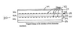
- FIG. 2A device 20 for storing embedded charge in accordance with embodiments of the present invention is illustrated in FIG. 2 .
- the device 20 for storing embedded chargeincludes layers of silicon dioxide (SiO 2 ) 22 and 24 disposed on opposing surfaces of a layer of silicon nitride (Si 3 N 4 ) 26 , although the device 20 can comprise other numbers and types of layers in other configurations, such as having layers 22 and 24 made of different materials.
- the present inventionutilizes very wide band gap insulating materials in conjunction with medium to low band gap insulating materials to significantly improve embedded charge high temperature trapped charge retention time.
- the device 20has a conductor 27 on the layer of silicon dioxide 22 which is on the layer of silicon nitride 26 which is on the layer of silicon dioxide 24 which is on a substrate 23 , although the device 20 for storing embedded charge could have other numbers and types of non-conducting and conducting layers.
- the layer of silicon nitride 26comprises a low to medium band gap insulating layer which is adjacent on opposing sides to the layers of silicon dioxide 22 and 24 which are the wide band gap insulating layers.
- the layer of silicon nitride 26has a band gap of approximately 5 eV and the layers of silicon dioxide 22 and 24 each have a band gap of approximately 9 eV.
- the layer of silicon nitride 26is shown as the low to medium band gap layer, other types of low to medium band gap layers can be used, such as a layer of titanium dioxide (TiO 2 ), strontium titanium oxide SrTiO 3 , zirconium oxide (ZrO 2 ), or barium titanium oxide (BaTiO 3 ). Additionally, although the layers of silicon dioxide 22 and 24 are shown as the wide band gap layers, other types of wide band gap layers can be used, such as layers of calcium fluoride (CaF 2 ), magnesium fluoride (MgF 2 ), lithium fluoride (LiF), or aluminum oxide (Al 2 O 3 ).
- CaF 2calcium fluoride
- MgF 2magnesium fluoride
- LiFlithium fluoride
- Al 2 O 3aluminum oxide
- An interface 28is formed between the layer of silicon dioxide 22 and the layer of silicon nitride 26 and an interface 30 is formed between the layer of silicon nitride 26 and the layer of silicon dioxide 24 .
- a fixed, static electronic charge 32 on the order of at least 1 ⁇ 10 10 charges/cm 2is stored at each of the interfaces 28 and 30 .
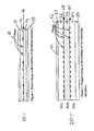
- the device 40 ( 1 )comprises a layer of silicon nitride 42 which is completely encased in a layer of silicon dioxide 44 with a conductor 45 on one surface 48 ( 1 ) of the layer of silicon dioxide 44 which is on the suitable substrate 43 , such as silicon, although the device 40 ( 1 ) could comprise other types and numbers of layers in other configurations, such as with or without the conductor 45 and/or the substrate 43 and with other configurations for the conductor 45 and/or substrate 43 .
- the layer of silicon dioxide 44has outer surfaces 48 ( 1 )- 48 ( 4 ), although the layer of silicon dioxide 44 could have other numbers of outer surfaces.
- the layer of silicon nitride 42has a band gap of approximately 5 eV and the layer of silicon dioxide 44 has a band gap of approximately 9 eV.
- a layer of silicon dioxide 44 and a layer of silicon nitride 42are used in this embodiment, again as described with reference to FIG. 2 , other types of dissimilar insulating materials with the band gap differences discussed herein can be used.
- Interfaces 46 ( 1 )- 46 ( 4 )are formed between the layer of silicon nitride 42 and the layer of silicon dioxide 44 .
- a fixed, static electronic charge 50 on the order of at least 1 ⁇ 10 10 charges/cm 2is stored at each of the interfaces 46 ( 1 ) and 46 ( 3 ), although the charge could be stored at other interfaces, such as interfaces 46 ( 2 ) and 46 ( 4 ), in other configurations.
- the charge retention and temperature robustness of the device 40 ( 1 )is further enhanced because the layer of silicon dioxide 44 surrounds all of the outer surfaces of the layer of silicon nitride 42 .
- FIG. 4another device 40 ( 2 ) for storing embedded fixed, static charge 52 with improved temperature robustness in accordance with embodiments of the present invention is illustrated. Elements in FIG. 4 which are like those shown and described in FIG. 3 will have like reference numerals.
- the device 40 ( 2 )comprises a layer of silicon nitride 42 is completely encased in a layer of calcium fluoride (CaF 2 ) 54 with a conductor 55 on one surface 58 ( 1 ) of the layer of calcium fluoride 54 and a suitable substrate 53 on another surface 58 ( 3 ) of the layer of calcium fluoride 54 , such as silicon, although the device 40 ( 2 ) could comprise other types and numbers of layers in other configurations, such as with or without the conductor 55 and/or the substrate 53 and with other configurations for the conductor 55 and/or substrate 53 .
- the layer of calcium fluoride 54has outer surfaces 58 ( 1 )- 58 ( 4 ), although the layer of calcium fluoride 54 could have other numbers of outer surfaces.
- the layer of calcium fluoride 54has a band gap of approximately 12.1 eV and the layer of silicon nitride 42 has a band gap of approximately 5 eV. Therefore, the encasing layer of calcium fluoride 54 provides a very high barrier around the entire outer surface of the layer of silicon nitride 42 that must be overcome before any trapped charge 52 at the interfaces 56 ( 1 ) and 56 ( 3 ) between the layer of calcium fluoride 54 and the layer of silicon nitride 42 is lost.
- a layer of calcium fluoride 54 and a layer of silicon nitride 42are used in this embodiment, again as described with reference to FIG. 2 , other types of dissimilar insulating materials with the band gap differences discussed herein can be used.
- Interfaces 56 ( 1 )- 56 ( 4 )are formed between the layer of silicon nitride 42 and the encasing layer of calcium fluoride 54 .
- a fixed, static electronic charge 52 on the order of at least 1 ⁇ 10 10 charges/cm 2is stored at each of the interfaces 56 ( 1 ) and 56 ( 3 ), although the charge could be stored at other interfaces, such as interfaces 56 ( 2 ) and 56 ( 4 ) in other configurations.
- the charge retention and temperature robustness of the device 40 ( 2 )is further enhanced because the layer of calcium fluoride 54 surrounds all of the outer surfaces of the layer of silicon nitride 42 .
- a device for storing embedded charge in accordance with the present inventionis a composite structure of dissimilar insulating materials or insulators that has a wide band gap insulating material encasing at least a portion of a lower band gap material.
- the wide band gap insulating materialshould have a band gap of over about 6.0 eV and the low to medium band gap material should have a band gap of about 5.5 eV or less.
- the selection of the dissimilar insulating materials for each of the layersmay be based at least partially on the relative permittivity of each of the dissimilar insulating materials.
- the permittivity of the wide band gap materialcould be lower than the permittivity of the low to medium band gap material to assist with charge retention.
- a method for making the device 20 for storing embedded charge 32 in accordance with embodiments of the present inventionwill now be described.
- a layer of wide band gap insulating materialcomprising silicon dioxide 24
- a layer of low to medium band gap materialcomprising silicon nitride 26 is deposited by Chemical Vapor Deposition (CVD), although other techniques for depositing layer 26 can be used, such as sputtering, evaporation, atomic layer epitaxy, and molecular beam epitaxy.
- CVDChemical Vapor Deposition
- a layer of wide band gap insulating materialcomprising silicon dioxide 22 is deposited on the layer silicon nitride 26 by Chemical Vapor Deposition (CVD), although other techniques for depositing layer 22 can be used, such as sputtering, evaporation, atomic layer epitaxy, and molecular beam epitaxy.
- CVDChemical Vapor Deposition
- a fixed, static electronic charge 32 on the order of at least 1 ⁇ 10 10 charges/cm 2is injected by high field injection into the device 20 and is trapped at the interfaces 28 and 30 , although other techniques for embedding the charge 32 , such as ballistic injection, can be used.
- a layer of silicon dioxide 44is deposited by Chemical Vapor Deposition (CVD) on a suitable substrate 43 , such as silicon although other materials could be used for the substrate 43 and the layer 44 could be formed in other manners.
- CVDChemical Vapor Deposition
- a layer of low to medium band gap material comprising silicon nitride 42is deposited on the layer of silicon dioxide 44 by CVD and is patterned to the shape shown, although other techniques for forming layer 42 can be used, such as sputtering, evaporation, atomic layer epitaxy, and molecular beam epitaxy or depositing the silicon nitride 42 in a trench in the layer of silicon dioxide 44 .
- more of the wide band gap insulating material comprising silicon dioxide 44is deposited to encase the layer of silicon nitride 42 .
- a fixed, static electronic charge 41 on the order of at least 1 ⁇ 10 10 charges/cm 2is injected by high field injection into the device 40 ( 1 ) and is trapped at the interfaces 46 ( 1 ) and 46 ( 3 ), although other techniques for embedding the charge 41 , such as ballistic injection, can be used.
- a layer of calcium fluoride 54is deposited by sputtering on a suitable substrate 53 , such as silicon although other materials could be used for the substrate 53 and the layer 54 could be formed in other manners.
- a layer of low to medium band gap material comprising silicon nitride 42is deposited on the layer of calcium fluoride 54 and by CVD and is patterned to the shape shown, although other techniques for forming layer 42 can be used, such as sputtering, evaporation, atomic layer epitaxy, and molecular beam epitaxy or depositing the silicon nitride 42 in a trench in the layer of calcium fluoride 54 .
- more of the wide band gap insulating material comprising calcium fluorideis deposited to encase the layer of silicon nitride 42 .
- a fixed, static electronic charge 52 on the order of at least 1 ⁇ 10 10 charges/cm 2is injected by high field injection into the device 40 ( 2 ) and is trapped at the interfaces 56 ( 1 ) and 56 ( 3 ), although other techniques for embedding the charge 52 , such as ballistic injection, can be used.
- the present inventionprovides a system and method for making local regions of embedded electronic charge with high temperature reliability.
- the present inventionutilizes very wide band gap insulating materials in conjunction with medium to low band gap insulating materials to significantly improve embedded charge high temperature trapped charge retention time.
- the present inventionis also easily integratable with standard integrated circuits and silicon carbide devices.
Landscapes
- Non-Volatile Memory (AREA)
- Semiconductor Memories (AREA)
Abstract
Description
This application claims the benefit of U.S. Provisional Patent Application Ser. No. 60/546,045, filed Feb. 19, 2004, which is hereby incorporated by reference in its entirety.
The present invention generally relates to devices for storing charge and, more particularly, to high temperature, embedded charge devices and methods thereof
Embedded charge technology is being exploited in numerous ways. The underlying science provides a platform for devices that range from micro sensors to macroscopic energy transducers. Embedded charge technology has excellent long-term reliability in environments where the temperature does not exceed a few hundred degrees Celsius.
Embedded charge technology utilizes electronic charge that is trapped at the interface of dissimilar insulators. Typically, systems employ insulators, such as silicon dioxide (SiO2)—silicon nitride (Si3N4), as continuous thin films. For applications in harsh environments with elevated temperatures above a few hundred degrees Celsius there is a need for significant improvement in overall temperature robustness.
An example ofprior device 10 for storing embedded charge with charge stored at the interface of dissimilar insulators is illustrated inFIG. 1 . Thedevice 10 has a layer ofsilicon dioxide 14 between asubstrate 13 and a layer ofsilicon nitride 12 and a conductor15 on the layer ofsilicon nitride 12. Electronic charge is stored at aninterface 16 between thelayers silicon nitride 12 is approximately 5 eV, whereas the band gap of the layer ofsilicon dioxide 14 is about 9 eV. In thisdevice 10, whenelectronic charge 18 is stored at theinterface 16 of thedissimilar insulators silicon nitride 12. However, when the surrounding temperature exceeds a few hundred degrees Celsius and/or thedevice 10 is placed in a high electric field, the retention of the embeddedcharge 18 in thisdevice 10 deteriorates and thecharge 18 can escape to the conductor15.
A device for storing embedded charge in accordance with embodiments of the present invention includes a first insulator and at least one second insulator. The first insulator has at least two outer surfaces and has a band gap of less than about 5.5 eV. The second insulator is deposited on at least each of the at least two outer surfaces of the first insulator to form at least one interface for storing charge between the first and second insulators. The second insulator has a band gap of more than about 6.0 eV.
A method for making a device for storing embedded charge in accordance with embodiments of the present invention includes providing a first insulator having at least two outer surfaces and depositing at least one second insulator on at least each of the at least two outer surfaces of the first insulator to form at least one interface for storing charge between the first and second insulators. The first insulator has a band gap of less than about 5.5 eV and the second insulator has a band gap of more than about 6.0 eV.
A device for storing embedded charge in accordance with embodiments of the present invention includes a first insulator and at least one second insulator which substantially encases the first insulator to form at least one interface for storing charge. The first insulator has a band gap of less than about 5.5 eV and the second insulator has a band gap of more than about 6.0 eV.
A method for making a device for storing embedded charge in accordance with embodiments of the present invention includes providing a first insulator and substantially encasing the first insulator with at least one second insulator to form at least one interface for storing charge between the first and second insulators. The first insulator having a band gap of less than about 5.5 eV and the second insulator having a band gap of more than about 6.0 eV
The present invention provides a system method for making local regions of embedded electronic charge with high temperature reliability. The present invention utilizes very wide band gap insulating materials in conjunction with medium to low band gap insulating materials to significantly improve embedded charge high temperature trapped charge retention time. The present invention also is easily integratable with standard integrated circuits and silicon carbide devices.
Adevice 20 for storing embedded charge in accordance with embodiments of the present invention is illustrated inFIG. 2 . Thedevice 20 for storing embedded charge includes layers of silicon dioxide (SiO2)22 and24 disposed on opposing surfaces of a layer of silicon nitride (Si3N4)26, although thedevice 20 can comprise other numbers and types of layers in other configurations, such as havinglayers
Referring more specifically toFIG. 2 , thedevice 20 has aconductor 27 on the layer ofsilicon dioxide 22 which is on the layer ofsilicon nitride 26 which is on the layer ofsilicon dioxide 24 which is on asubstrate 23, although thedevice 20 for storing embedded charge could have other numbers and types of non-conducting and conducting layers. The layer ofsilicon nitride 26 comprises a low to medium band gap insulating layer which is adjacent on opposing sides to the layers ofsilicon dioxide silicon nitride 26 has a band gap of approximately 5 eV and the layers ofsilicon dioxide silicon nitride 26 is shown as the low to medium band gap layer, other types of low to medium band gap layers can be used, such as a layer of titanium dioxide (TiO2), strontium titanium oxide SrTiO3, zirconium oxide (ZrO2), or barium titanium oxide (BaTiO3). Additionally, although the layers ofsilicon dioxide
Aninterface 28 is formed between the layer ofsilicon dioxide 22 and the layer ofsilicon nitride 26 and aninterface 30 is formed between the layer ofsilicon nitride 26 and the layer ofsilicon dioxide 24. A fixed, staticelectronic charge 32 on the order of at least 1×10¹⁰charges/cm2is stored at each of theinterfaces
With thisdevice 20 for storing embedded fixed,static charge 32, charge loss at elevated temperature environmental conditions for charge trapped at theinterfaces layers silicon dioxide silicon nitride 26. However, because it is difficult for the charge to travel through the layers ofsilicon dioxide silicon nitride 26, the embedded fixed,static charge 32 remains at theinterfaces
Referring toFIG. 3 , another device40(1) for storing embedded, fixed,static charge 41 with improved temperature robustness in accordance with embodiments of the present invention is illustrated. The device40(1) comprises a layer ofsilicon nitride 42 which is completely encased in a layer ofsilicon dioxide 44 with aconductor 45 on one surface48(1) of the layer ofsilicon dioxide 44 which is on thesuitable substrate 43, such as silicon, although the device40(1) could comprise other types and numbers of layers in other configurations, such as with or without theconductor 45 and/or thesubstrate 43 and with other configurations for theconductor 45 and/orsubstrate 43. The layer ofsilicon dioxide 44 has outer surfaces48(1)-48(4), although the layer ofsilicon dioxide 44 could have other numbers of outer surfaces. The layer ofsilicon nitride 42 has a band gap of approximately 5 eV and the layer ofsilicon dioxide 44 has a band gap of approximately 9 eV. Although a layer ofsilicon dioxide 44 and a layer ofsilicon nitride 42 are used in this embodiment, again as described with reference toFIG. 2 , other types of dissimilar insulating materials with the band gap differences discussed herein can be used.
Interfaces46(1)-46(4) are formed between the layer ofsilicon nitride 42 and the layer ofsilicon dioxide 44. A fixed, static electronic charge50 on the order of at least 1×10¹⁰charges/cm2is stored at each of the interfaces46(1) and46(3), although the charge could be stored at other interfaces, such as interfaces46(2) and46(4), in other configurations. Again, the charge retention and temperature robustness of the device40(1) is further enhanced because the layer ofsilicon dioxide 44 surrounds all of the outer surfaces of the layer ofsilicon nitride 42.
Referring toFIG. 4 , another device40(2) for storing embedded fixed,static charge 52 with improved temperature robustness in accordance with embodiments of the present invention is illustrated. Elements inFIG. 4 which are like those shown and described inFIG. 3 will have like reference numerals. The device40(2) comprises a layer ofsilicon nitride 42 is completely encased in a layer of calcium fluoride (CaF2)54 with aconductor 55 on one surface58(1) of the layer ofcalcium fluoride 54 and asuitable substrate 53 on another surface58(3) of the layer ofcalcium fluoride 54, such as silicon, although the device40(2) could comprise other types and numbers of layers in other configurations, such as with or without theconductor 55 and/or thesubstrate 53 and with other configurations for theconductor 55 and/orsubstrate 53. The layer ofcalcium fluoride 54 has outer surfaces58(1)-58(4), although the layer ofcalcium fluoride 54 could have other numbers of outer surfaces. The layer ofcalcium fluoride 54 has a band gap of approximately 12.1 eV and the layer ofsilicon nitride 42 has a band gap of approximately 5 eV. Therefore, the encasing layer ofcalcium fluoride 54 provides a very high barrier around the entire outer surface of the layer ofsilicon nitride 42 that must be overcome before any trappedcharge 52 at the interfaces56(1) and56(3) between the layer ofcalcium fluoride 54 and the layer ofsilicon nitride 42 is lost. Although a layer ofcalcium fluoride 54 and a layer ofsilicon nitride 42 are used in this embodiment, again as described with reference toFIG. 2 , other types of dissimilar insulating materials with the band gap differences discussed herein can be used.
Interfaces56(1)-56(4) are formed between the layer ofsilicon nitride 42 and the encasing layer ofcalcium fluoride 54. A fixed, staticelectronic charge 52 on the order of at least 1×10¹⁰charges/cm2is stored at each of the interfaces56(1) and56(3), although the charge could be stored at other interfaces, such as interfaces56(2) and56(4) in other configurations. Again, the charge retention and temperature robustness of the device40(2) is further enhanced because the layer ofcalcium fluoride 54 surrounds all of the outer surfaces of the layer ofsilicon nitride 42.
Accordingly, a device for storing embedded charge in accordance with the present invention is a composite structure of dissimilar insulating materials or insulators that has a wide band gap insulating material encasing at least a portion of a lower band gap material. In these embodiments, the wide band gap insulating material should have a band gap of over about 6.0 eV and the low to medium band gap material should have a band gap of about 5.5 eV or less. Additionally, the selection of the dissimilar insulating materials for each of the layers may be based at least partially on the relative permittivity of each of the dissimilar insulating materials. In these embodiments, the permittivity of the wide band gap material could be lower than the permittivity of the low to medium band gap material to assist with charge retention.
Referring toFIG. 2 , a method for making thedevice 20 for storing embeddedcharge 32 in accordance with embodiments of the present invention will now be described. On a suitable substrate a layer of wide band gap insulating material comprisingsilicon dioxide 24, a layer of low to medium band gap material comprisingsilicon nitride 26 is deposited by Chemical Vapor Deposition (CVD), although other techniques for depositinglayer 26 can be used, such as sputtering, evaporation, atomic layer epitaxy, and molecular beam epitaxy. Next, another layer of wide band gap insulating material comprisingsilicon dioxide 22 is deposited on thelayer silicon nitride 26 by Chemical Vapor Deposition (CVD), although other techniques for depositinglayer 22 can be used, such as sputtering, evaporation, atomic layer epitaxy, and molecular beam epitaxy. Next, a fixed, staticelectronic charge 32 on the order of at least 1×10¹⁰charges/cm2is injected by high field injection into thedevice 20 and is trapped at theinterfaces charge 32, such as ballistic injection, can be used.
Referring toFIG. 3 , a method for making the device40(1) for storing embeddedcharge 41 in accordance with embodiments of the present invention will now be described. A layer ofsilicon dioxide 44 is deposited by Chemical Vapor Deposition (CVD) on asuitable substrate 43, such as silicon although other materials could be used for thesubstrate 43 and thelayer 44 could be formed in other manners. A layer of low to medium band gap material comprisingsilicon nitride 42 is deposited on the layer ofsilicon dioxide 44 by CVD and is patterned to the shape shown, although other techniques for forminglayer 42 can be used, such as sputtering, evaporation, atomic layer epitaxy, and molecular beam epitaxy or depositing thesilicon nitride 42 in a trench in the layer ofsilicon dioxide 44. Next, more of the wide band gap insulating material comprisingsilicon dioxide 44 is deposited to encase the layer ofsilicon nitride 42. Once the layer ofsilicon nitride 42 is encased, a fixed, staticelectronic charge 41 on the order of at least 1×10¹⁰charges/cm2is injected by high field injection into the device40(1) and is trapped at the interfaces46(1) and46(3), although other techniques for embedding thecharge 41, such as ballistic injection, can be used.
Referring toFIG. 4 , a method for making the device40(2) for storing embeddedcharge 52 in accordance with embodiments of the present invention will now be described. A layer ofcalcium fluoride 54 is deposited by sputtering on asuitable substrate 53, such as silicon although other materials could be used for thesubstrate 53 and thelayer 54 could be formed in other manners. A layer of low to medium band gap material comprisingsilicon nitride 42 is deposited on the layer ofcalcium fluoride 54 and by CVD and is patterned to the shape shown, although other techniques for forminglayer 42 can be used, such as sputtering, evaporation, atomic layer epitaxy, and molecular beam epitaxy or depositing thesilicon nitride 42 in a trench in the layer ofcalcium fluoride 54. Next, more of the wide band gap insulating material comprising calcium fluoride is deposited to encase the layer ofsilicon nitride 42. Next, a fixed, staticelectronic charge 52 on the order of at least 1×10¹⁰charges/cm2is injected by high field injection into the device40(2) and is trapped at the interfaces56(1) and56(3), although other techniques for embedding thecharge 52, such as ballistic injection, can be used.
Accordingly, the present invention provides a system and method for making local regions of embedded electronic charge with high temperature reliability. The present invention utilizes very wide band gap insulating materials in conjunction with medium to low band gap insulating materials to significantly improve embedded charge high temperature trapped charge retention time. The present invention is also easily integratable with standard integrated circuits and silicon carbide devices.
Having thus described the basic concept of the invention, it will be rather apparent to those skilled in the art that the foregoing detailed disclosure is intended to be presented by way of example only, and is not limiting. Various alterations, improvements, and modifications will occur and are intended to those skilled in the art, though not expressly stated herein. These alterations, improvements, and modifications are intended to be suggested hereby, and are within the spirit and scope of the invention. Additionally, the recited order of processing elements or sequences, or the use of numbers, letters, or other designations therefore, is not intended to limit the claimed processes to any order except as may be specified in the claims. Accordingly, the invention is limited only by the following claims and equivalents thereto.
Claims (9)
1. A device for storing embedded charge comprising:
a first insulator having at least two outer surfaces, the first insulator having a band gap of less than about 5.5 eV; and
at least one second insulator on at least each of the at least two outer surfaces of the first insulator to form at least one interface between the first and second insulators and has a band gap of more than about 6.0 eV; and
injected, fixed, static electronic charge in addition to inherent formation charge stored at the at least one interface, wherein the injected, fixed, static electronic charge at the at least one interface between the first and second insulators is negative, fixed static electronic charge and further consisting of no more than one continuous conductor structure on the second; insulator.
2. The device as set forth inclaim 1 wherein the first insulator is selected from a group consisting of Si3N4, TiO2, SrTiO3, ZrO2, and BaTiO3and the second insulator is selected from a group consisting of SiO2, CaF2, MgF2, LiF, and Al2O3.
3. The device as set forth inclaim 1 wherein the second insulator comprises at least two layers, each of the layers of the second insulator are on a different one of the outer surfaces of the first insulator.
4. The device as set forth inclaim 1 wherein the second insulator against one of one or more surfaces of the first insulator is the same as the second insulator against all other surfaces of the first insulator and substantially encases the first insulator.
5. The device as set forth inclaim 1 wherein the band gap of the second insulator is at least double the band gap of the first insulator.
6. The device as set forth inclaim 1 wherein a permittivity of the second insulator is lower than a permittivity of the first insulator.
7. The device as set forth inclaim 5 wherein the second insulator comprises a non-oxide insulating layer.
8. The device as set forth inclaim 7 wherein the non-oxide insulating layer is selected from a group consisting of CaF2MgF2, and LiF.
9. The device as set forth inclaim 1 wherein the injected, fixed, static, electronic charge further comprises at least one of high field injected and ballistic injected, fixed, static, electronic charge on the order of at least 1×10¹⁰charges/cm2stored at the at least one interface.
Priority Applications (1)
| Application Number | Priority Date | Filing Date | Title |
|---|---|---|---|
| US11/059,882US8581308B2 (en) | 2004-02-19 | 2005-02-17 | High temperature embedded charge devices and methods thereof |
Applications Claiming Priority (2)
| Application Number | Priority Date | Filing Date | Title |
|---|---|---|---|
| US54604504P | 2004-02-19 | 2004-02-19 | |
| US11/059,882US8581308B2 (en) | 2004-02-19 | 2005-02-17 | High temperature embedded charge devices and methods thereof |
Publications (2)
| Publication Number | Publication Date |
|---|---|
| US20050205966A1 US20050205966A1 (en) | 2005-09-22 |
| US8581308B2true US8581308B2 (en) | 2013-11-12 |
Family
ID=34985355
Family Applications (1)
| Application Number | Title | Priority Date | Filing Date |
|---|---|---|---|
| US11/059,882Expired - Fee RelatedUS8581308B2 (en) | 2004-02-19 | 2005-02-17 | High temperature embedded charge devices and methods thereof |
Country Status (1)
| Country | Link |
|---|---|
| US (1) | US8581308B2 (en) |
Cited By (3)
| Publication number | Priority date | Publication date | Assignee | Title |
|---|---|---|---|---|
| US20170170674A1 (en)* | 2015-12-09 | 2017-06-15 | Nth Tech Corporation | Methods for trapping electrons at an interface of insulators each having an arbitrary thickness and devices thereof |
| US10811503B2 (en) | 2016-09-06 | 2020-10-20 | Becsis, Llc | Electrostatic catalysis |
| US10879027B2 (en) | 2017-03-06 | 2020-12-29 | Becsis, Llc | High energy X-ray generation without the use of a high voltage power supply |
Families Citing this family (9)
| Publication number | Priority date | Publication date | Assignee | Title |
|---|---|---|---|---|
| US7280014B2 (en) | 2001-03-13 | 2007-10-09 | Rochester Institute Of Technology | Micro-electro-mechanical switch and a method of using and making thereof |
| WO2002097865A2 (en)* | 2001-05-31 | 2002-12-05 | Rochester Institute Of Technology | Fluidic valves, agitators, and pumps and methods thereof |
| US7378775B2 (en) | 2001-10-26 | 2008-05-27 | Nth Tech Corporation | Motion based, electrostatic power source and methods thereof |
| US7211923B2 (en) | 2001-10-26 | 2007-05-01 | Nth Tech Corporation | Rotational motion based, electrostatic power source and methods thereof |
| US20050132549A1 (en)* | 2001-11-16 | 2005-06-23 | Wong-Cheng Shih | Method for making metal capacitors with low leakage currents for mixed-signal devices |
| US7217582B2 (en) | 2003-08-29 | 2007-05-15 | Rochester Institute Of Technology | Method for non-damaging charge injection and a system thereof |
| US7287328B2 (en) | 2003-08-29 | 2007-10-30 | Rochester Institute Of Technology | Methods for distributed electrode injection |
| JP2016066641A (en)* | 2014-09-22 | 2016-04-28 | 株式会社東芝 | Semiconductor device and method of manufacturing the same |
| US20170323885A1 (en)* | 2016-04-18 | 2017-11-09 | North Carolina State University | High quality varactor |
Citations (223)
| Publication number | Priority date | Publication date | Assignee | Title |
|---|---|---|---|---|
| US2567373A (en) | 1949-06-10 | 1951-09-11 | Rca Corp | Electrostatic generator |
| US2588513A (en) | 1949-06-10 | 1952-03-11 | Rca Corp | Electrostatic high-voltage generator |
| US2978066A (en) | 1959-05-07 | 1961-04-04 | Honeywell Regulator Co | Gas cleaning apparatus |
| US3118022A (en) | 1961-08-07 | 1964-01-14 | Bell Telephone Labor Inc | Electroacoustic transducer |
| US3397278A (en) | 1965-05-06 | 1968-08-13 | Mallory & Co Inc P R | Anodic bonding |
| US3405334A (en) | 1967-03-06 | 1968-10-08 | Homer H. Jewett | Electrostatic power generator driven by pneumatic power means |
| US3487610A (en) | 1965-03-26 | 1970-01-06 | Du Pont | Electrostatic filter unit with high stable charge and its manufacture |
| US3715500A (en) | 1971-07-21 | 1973-02-06 | Bell Telephone Labor Inc | Unidirectional microphones |
| US3731163A (en) | 1972-03-22 | 1973-05-01 | United Aircraft Corp | Low voltage charge storage memory element |
| US3742767A (en) | 1971-02-02 | 1973-07-03 | Onera (Off Nat Aerospatiale) | Ball electrostatic accelerometer |
| US3786495A (en) | 1972-05-17 | 1974-01-15 | Ncr | Stored charge transducer |
| US3858307A (en) | 1969-12-11 | 1975-01-07 | Matsushita Electric Industrial Co Ltd | Electrostatic transducer |
| US3924324A (en) | 1973-07-05 | 1975-12-09 | Sony Corp | Method of making electret |
| US4047214A (en) | 1975-09-04 | 1977-09-06 | Westinghouse Electric Corporation | Electrostatically bonded dielectric-on-semiconductor device, and a method of making the same |
| US4102202A (en) | 1976-11-26 | 1978-07-25 | The Singer Company | Electrostatic accelerometer |
| US4115914A (en) | 1976-03-26 | 1978-09-26 | Hughes Aircraft Company | Electrically erasable non-volatile semiconductor memory |
| US4126822A (en) | 1977-05-27 | 1978-11-21 | Wahlstrom Sven E | Electrostatic generator and motor |
| US4160882A (en) | 1978-03-13 | 1979-07-10 | Driver Michael L | Double diaphragm electrostatic transducer each diaphragm comprising two plastic sheets having different charge carrying characteristics |
| US4166729A (en) | 1977-07-26 | 1979-09-04 | The United States Of America As Represented By The Secretary Of The Navy | Collector plates for electrostatic precipitators |
| US4285714A (en) | 1978-12-07 | 1981-08-25 | Spire Corporation | Electrostatic bonding using externally applied pressure |
| US4288735A (en) | 1979-09-17 | 1981-09-08 | Mcdonnell Douglas Corp. | Vibrating electret reed voltage generator |
| US4340953A (en) | 1979-05-14 | 1982-07-20 | Nippon Hoso Kyokai | Information recording medium and recording and reproducing system using the same |
| US4375718A (en) | 1981-03-12 | 1983-03-08 | Surgikos, Inc. | Method of making fibrous electrets |
| US4490772A (en) | 1983-06-13 | 1984-12-25 | Blickstein Martin J | Voltage and mechanically variable trimmer capacitor |
| US4504550A (en) | 1982-07-21 | 1985-03-12 | James Frederick John Johnson | Releasably mutually-adherent materials |
| US4513049A (en) | 1983-04-26 | 1985-04-23 | Mitsui Petrochemical Industries, Ltd. | Electret article |
| US4581624A (en) | 1984-03-01 | 1986-04-08 | Allied Corporation | Microminiature semiconductor valve |
| US4585209A (en) | 1983-10-27 | 1986-04-29 | Harry E. Aine | Miniature valve and method of making same |
| US4626263A (en) | 1984-04-24 | 1986-12-02 | Mitsui Petrochemical Industries, Ltd. | High-performance electret and air filter |
| US4626729A (en) | 1984-05-04 | 1986-12-02 | Jacques Lewiner | Electroacoustic piezoelectric transducers |
| US4701640A (en) | 1985-03-11 | 1987-10-20 | Telex Communications, Inc. | Electret transducer and method of fabrication |
| US4716331A (en) | 1985-12-30 | 1987-12-29 | Motorola Inc. | Electrically variable piezoelectric hybrid capacitor |
| US4736629A (en) | 1985-12-20 | 1988-04-12 | Silicon Designs, Inc. | Micro-miniature accelerometer |
| US4789504A (en) | 1984-03-19 | 1988-12-06 | Toyo Boseki Kabushiki Kaisha | Electretized material for a dust filter |
| US4789803A (en) | 1987-08-04 | 1988-12-06 | Sarcos, Inc. | Micropositioner systems and methods |
| US4794370A (en) | 1984-08-21 | 1988-12-27 | Bos-Knox Ltd. | Peristaltic electrostatic binary device |
| US4874659A (en) | 1984-10-24 | 1989-10-17 | Toray Industries | Electret fiber sheet and method of producing same |
| US4905701A (en) | 1988-06-15 | 1990-03-06 | National Research Development Corporation | Apparatus and method for detecting small changes in attached mass of piezoelectric devices used as sensors |
| US4922756A (en) | 1988-06-20 | 1990-05-08 | Triton Technologies, Inc. | Micro-machined accelerometer |
| US4945068A (en) | 1988-10-25 | 1990-07-31 | Matsushita Electronics Corporation | Manufacturing method of semiconductor nonvolatile memory device |
| US4944854A (en) | 1983-11-08 | 1990-07-31 | Celanese Corporation | Electret process and products |
| US4945393A (en)* | 1988-06-21 | 1990-07-31 | At&T Bell Laboratories | Floating gate memory circuit and apparatus |
| US4958317A (en) | 1987-07-27 | 1990-09-18 | Mitsubishi Denki Kabushiki Kaisha | Nonvolatile semiconductor memory device and a writing method using electron tunneling |
| US4965244A (en)* | 1988-09-19 | 1990-10-23 | Regents Of The University Of Minnesota | CaF2 passivation layers for high temperature superconductors |
| US4996627A (en) | 1989-01-30 | 1991-02-26 | Dresser Industries, Inc. | High sensitivity miniature pressure transducer |
| US4997521A (en) | 1987-05-20 | 1991-03-05 | Massachusetts Institute Of Technology | Electrostatic micromotor |
| US5020030A (en) | 1988-10-31 | 1991-05-28 | Huber Robert J | Nonvolatile SNOS memory cell with induced capacitor |
| US5051643A (en) | 1990-08-30 | 1991-09-24 | Motorola, Inc. | Electrostatically switched integrated relay and capacitor |
| US5050435A (en) | 1989-07-18 | 1991-09-24 | The Boeing Company | Position detection system for a suspended particle accelerometer |
| US5054081A (en) | 1985-04-02 | 1991-10-01 | West Roger A | Electrostatic transducer with improved bass response utilizing disturbed bass resonance energy |
| US5057710A (en) | 1988-05-13 | 1991-10-15 | Toray Industries, Inc. | Electret materials and the method for preparing the electret materials |
| US5081513A (en) | 1991-02-28 | 1992-01-14 | Xerox Corporation | Electronic device with recovery layer proximate to active layer |
| US5082242A (en) | 1989-12-27 | 1992-01-21 | Ulrich Bonne | Electronic microvalve apparatus and fabrication |
| US5088326A (en) | 1989-05-24 | 1992-02-18 | Mitsubishi Denki K.K. | Piezoelectric accelerometer for automobiles |
| US5092174A (en) | 1989-10-19 | 1992-03-03 | Texas Instruments Incorporated | Capacitance accelerometer |
| US5095752A (en) | 1988-11-15 | 1992-03-17 | Hitachi, Ltd. | Capacitance type accelerometer |
| US5096388A (en) | 1990-03-22 | 1992-03-17 | The Charles Stark Draper Laboratory, Inc. | Microfabricated pump |
| US5108470A (en) | 1988-11-01 | 1992-04-28 | William Pick | Charging element having odor and gas absorbing properties for an electrostatic air filter |
| US5112677A (en) | 1987-11-28 | 1992-05-12 | Toyo Boseki Kabushiki Kaisha | Electret sheet and a method for the production of the same |
| US5118942A (en) | 1990-02-05 | 1992-06-02 | Hamade Thomas A | Electrostatic charging apparatus and method |
| US5129794A (en) | 1990-10-30 | 1992-07-14 | Hewlett-Packard Company | Pump apparatus |
| US5132934A (en) | 1989-06-23 | 1992-07-21 | The Board Of Trustees Of The Leland Stanford Junior University | Method and apparatus for storing digital information in the form of stored charges |
| US5143854A (en) | 1989-06-07 | 1992-09-01 | Affymax Technologies N.V. | Large scale photolithographic solid phase synthesis of polypeptides and receptor binding screening thereof |
| US5156810A (en) | 1989-06-15 | 1992-10-20 | Biocircuits Corporation | Biosensors employing electrical, optical and mechanical signals |
| US5164319A (en) | 1985-08-22 | 1992-11-17 | Molecular Devices Corporation | Multiple chemically modulated capacitance determination |
| US5180623A (en) | 1989-12-27 | 1993-01-19 | Honeywell Inc. | Electronic microvalve apparatus and fabrication |
| US5189641A (en) | 1987-06-08 | 1993-02-23 | Fujitsu Limited | Non-volatile random access memory device |
| US5207103A (en) | 1987-06-01 | 1993-05-04 | Wise Kensall D | Ultraminiature single-crystal sensor with movable member |
| US5228373A (en) | 1990-01-08 | 1993-07-20 | Robert A. Foisie | Method and apparatus using electrostatic charges to temporarily hold packets of paper |
| US5231045A (en) | 1988-12-08 | 1993-07-27 | Fujitsu Limited | Method of producing semiconductor-on-insulator structure by besol process with charged insulating layers |
| US5238223A (en) | 1989-08-11 | 1993-08-24 | Robert Bosch Gmbh | Method of making a microvalve |
| US5256176A (en) | 1990-03-12 | 1993-10-26 | Mitsui Petrochemical Industries, Ltd. | Film electret and an electret filter |
| US5262000A (en) | 1989-09-26 | 1993-11-16 | British Telecommunications Public Limited Company | Method for making micromechanical switch |
| US5284692A (en) | 1991-10-24 | 1994-02-08 | Bell Dennis J | Electrostatic evacuated insulating sheet |
| US5284179A (en) | 1991-05-30 | 1994-02-08 | Hitachi, Ltd. | Valve and semiconductor fabricating equipment using the same |
| US5323999A (en) | 1991-08-08 | 1994-06-28 | Honeywell Inc. | Microstructure gas valve control |
| US5334238A (en) | 1990-11-27 | 1994-08-02 | United Technologies Corporation | Cleaner method for electrostatic precipitator |
| US5336062A (en) | 1990-02-27 | 1994-08-09 | Fraunhofer-Gesellschaft Zur Forderung Der Angewandten Forschung E.V. | Microminiaturized pump |
| US5336904A (en)* | 1991-05-10 | 1994-08-09 | Mitsubishi Denki Kabushiki Kaisha | Field effect element utilizing resonant-tunneling and a method of manufacturing the same |
| US5348571A (en) | 1992-01-09 | 1994-09-20 | Metallgesellschaft Aktiengesellschaft | Apparatus for dedusting a gas at high temperature |
| US5349492A (en) | 1991-12-26 | 1994-09-20 | Yamatake-Honeywell Co., Ltd. | Capacitive pressure sensor |
| US5355577A (en) | 1992-06-23 | 1994-10-18 | Cohn Michael B | Method and apparatus for the assembly of microfabricated devices |
| US5367429A (en) | 1991-10-18 | 1994-11-22 | Hitachi, Ltd | Electrostatic type micro transducer and control system using the same |
| US5365790A (en) | 1992-04-02 | 1994-11-22 | Motorola, Inc. | Device with bonded conductive and insulating substrates and method therefore |
| US5392650A (en) | 1991-01-11 | 1995-02-28 | Northrop Grumman Corporation | Micromachined accelerometer gyroscope |
| US5417235A (en) | 1993-07-28 | 1995-05-23 | Regents Of The University Of Michigan | Integrated microvalve structures with monolithic microflow controller |
| US5417312A (en) | 1990-05-30 | 1995-05-23 | Hitachi, Ltd. | Semiconductor acceleration sensor and vehicle control system using the same |
| US5419953A (en) | 1993-05-20 | 1995-05-30 | Chapman; Rick L. | Multilayer composite air filtration media |
| US5434109A (en)* | 1993-04-27 | 1995-07-18 | International Business Machines Corporation | Oxidation of silicon nitride in semiconductor devices |
| US5441597A (en) | 1992-12-01 | 1995-08-15 | Honeywell Inc. | Microstructure gas valve control forming method |
| US5445008A (en) | 1994-03-24 | 1995-08-29 | Martin Marietta Energy Systems, Inc. | Microbar sensor |
| US5474599A (en) | 1992-08-11 | 1995-12-12 | United Air Specialists, Inc. | Apparatus for electrostatically cleaning particulates from air |
| US5488864A (en) | 1994-12-19 | 1996-02-06 | Ford Motor Company | Torsion beam accelerometer with slotted tilt plate |
| US5491604A (en) | 1992-12-11 | 1996-02-13 | The Regents Of The University Of California | Q-controlled microresonators and tunable electronic filters using such resonators |
| US5496507A (en) | 1993-08-17 | 1996-03-05 | Minnesota Mining And Manufacturing Company | Method of charging electret filter media |
| US5512882A (en) | 1991-08-07 | 1996-04-30 | Transducer Research, Inc. | Chemical sensing apparatus and methods |
| US5519240A (en) | 1993-02-26 | 1996-05-21 | Nec Corporation | Microshutter horizontally movable by electrostatic repulsion |
| US5520522A (en) | 1993-10-01 | 1996-05-28 | Tdk Corporation | Valve arrangement for a micro pump |
| US5526172A (en) | 1993-07-27 | 1996-06-11 | Texas Instruments Incorporated | Microminiature, monolithic, variable electrical signal processor and apparatus including same |
| US5567336A (en) | 1994-10-24 | 1996-10-22 | Matsushita Electric Industrial Co., Ltd. | Laser ablation forward metal deposition with electrostatic assisted bonding |
| US5578976A (en) | 1995-06-22 | 1996-11-26 | Rockwell International Corporation | Micro electromechanical RF switch |
| US5591679A (en) | 1995-04-12 | 1997-01-07 | Sensonor A/S | Sealed cavity arrangement method |
| US5593479A (en) | 1995-02-02 | 1997-01-14 | Hmi Industries, Inc. | Filter system |
| US5593476A (en) | 1994-06-09 | 1997-01-14 | Coppom Technologies | Method and apparatus for use in electronically enhanced air filtration |
| US5596194A (en) | 1994-08-19 | 1997-01-21 | Hughes Aircraft Company | Single-wafer tunneling sensor and low-cost IC manufacturing method |
| US5616844A (en) | 1993-12-27 | 1997-04-01 | Hitachi, Ltd. | Capacitance type acceleration sensor |
| US5635739A (en) | 1990-02-14 | 1997-06-03 | The Charles Stark Draper Laboratory, Inc. | Micromechanical angular accelerometer with auxiliary linear accelerometer |
| US5640133A (en) | 1995-06-23 | 1997-06-17 | Cornell Research Foundation, Inc. | Capacitance based tunable micromechanical resonators |
| WO1997031506A1 (en) | 1996-02-26 | 1997-08-28 | Panphonics Oy | Acoustic element and method for sound processing |
| US5668303A (en) | 1992-04-30 | 1997-09-16 | Forschung E.V Fraunhofer-Gesellschaft Zur Foerderung Der Angewandten | Sensor having a membrane as part of an electromechanical resonance circuit forming receiver and transmitter converter with interdigital structures spaced apart from one another |
| US5671905A (en) | 1995-06-21 | 1997-09-30 | Hopkins, Jr.; Dean A. | Electrochemical actuator and method of making same |
| US5677617A (en) | 1994-09-16 | 1997-10-14 | Kabushiki Kaisha Toshiba | Micro power supply device using switching element |
| US5698771A (en) | 1995-03-30 | 1997-12-16 | The United States Of America As Represented By The United States National Aeronautics And Space Administration | Varying potential silicon carbide gas sensor |
| US5739834A (en) | 1989-11-29 | 1998-04-14 | Dai Nippon Printing Co., Ltd. | Electrostatic charge information reproducing method |
| US5747692A (en) | 1991-01-28 | 1998-05-05 | Sarcos Group | Sensor system for determining acceleration |
| US5771148A (en) | 1995-11-17 | 1998-06-23 | Motorola, Inc. | Intercalation-based voltage variable capacitor |
| US5777977A (en) | 1995-08-23 | 1998-07-07 | Sony Corporation | Recording and reproducing apparatus |
| US5788468A (en) | 1994-11-03 | 1998-08-04 | Memstek Products, Llc | Microfabricated fluidic devices |
| US5793485A (en) | 1995-03-20 | 1998-08-11 | Sandia Corporation | Resonant-cavity apparatus for cytometry or particle analysis |
| US5798146A (en) | 1995-09-14 | 1998-08-25 | Tri-Star Technologies | Surface charging to improve wettability |
| US5807425A (en) | 1993-07-17 | 1998-09-15 | Gibbs; Robert William | Electrofilter |
| US5812163A (en) | 1996-02-13 | 1998-09-22 | Hewlett-Packard Company | Ink jet printer firing assembly with flexible film expeller |
| US5839062A (en) | 1994-03-18 | 1998-11-17 | The Regents Of The University Of California | Mixing, modulation and demodulation via electromechanical resonators |
| US5846302A (en) | 1997-04-24 | 1998-12-08 | Aqua-Air Technologies, Inc. | Electrostatic air filter device |
| US5846708A (en) | 1991-11-19 | 1998-12-08 | Massachusetts Institiute Of Technology | Optical and electrical methods and apparatus for molecule detection |
| US5871567A (en) | 1996-12-12 | 1999-02-16 | Dana Corporation | Dual Media air filter with electrostatic charge |
| US5874675A (en) | 1997-03-20 | 1999-02-23 | Interscience, Inc. | Wideband vibration sensor |
| US5897097A (en) | 1996-09-06 | 1999-04-27 | Xerox Corporation | Passively addressable fluid valves having S-shaped blocking films |
| US5908603A (en) | 1997-07-03 | 1999-06-01 | Industrial Technology Research Institute | Ozone generator having micro pump |
| US5914553A (en) | 1997-06-16 | 1999-06-22 | Cornell Research Foundation, Inc. | Multistable tunable micromechanical resonators |
| US5919364A (en) | 1996-06-24 | 1999-07-06 | Regents Of The University Of California | Microfabricated filter and shell constructed with a permeable membrane |
| US5920011A (en) | 1991-02-08 | 1999-07-06 | Alliedsignal Inc. | Micromachined rate and acceleration sensor |
| US5941501A (en) | 1996-09-06 | 1999-08-24 | Xerox Corporation | Passively addressable cantilever valves |
| US5959516A (en) | 1998-01-08 | 1999-09-28 | Rockwell Science Center, Llc | Tunable-trimmable micro electro mechanical system (MEMS) capacitor |
| US5969250A (en) | 1990-10-17 | 1999-10-19 | The Charles Stark Draper Laboratory, Inc. | Micromechanical accelerometer having a peripherally suspended proof mass |
| US5967163A (en) | 1996-01-30 | 1999-10-19 | Abbott Laboratories | Actuator and method |
| US5971355A (en) | 1996-11-27 | 1999-10-26 | Xerox Corporation | Microdevice valve structures to fluid control |
| US5994982A (en) | 1997-07-18 | 1999-11-30 | Trw Inc. | MEMS switched resonators for VCO applications |
| US5993520A (en) | 1998-01-16 | 1999-11-30 | Yu; Chi-Chin | Electronic dust collecting type air purifier |
| US6007309A (en) | 1995-12-13 | 1999-12-28 | Hartley; Frank T. | Micromachined peristaltic pumps |
| US6016092A (en) | 1997-08-22 | 2000-01-18 | Qiu; Cindy Xing | Miniature electromagnetic microwave switches and switch arrays |
| US6018170A (en)* | 1996-06-28 | 2000-01-25 | Nec Corporation | Single-layer-electrode type two-phase charge coupled device having smooth charge transfer |
| US6033852A (en) | 1996-09-27 | 2000-03-07 | University Of Maine | Monolithic piezoelectric sensor (MPS) for sensing chemical, biochemical and physical measurands |
| US6032923A (en) | 1998-01-08 | 2000-03-07 | Xerox Corporation | Fluid valves having cantilevered blocking films |
| US6037797A (en) | 1997-07-11 | 2000-03-14 | Semiconductor Diagnostics, Inc. | Measurement of the interface trap charge in an oxide semiconductor layer interface |
| US6040611A (en) | 1998-09-10 | 2000-03-21 | Hughes Electonics Corporation | Microelectromechanical device |
| US6043727A (en) | 1998-05-15 | 2000-03-28 | Hughes Electronics Corporation | Reconfigurable millimeterwave filter using stubs and stub extensions selectively coupled using voltage actuated micro-electro-mechanical switches |
| US6046659A (en) | 1998-05-15 | 2000-04-04 | Hughes Electronics Corporation | Design and fabrication of broadband surface-micromachined micro-electro-mechanical switches for microwave and millimeter-wave applications |
| US6048692A (en) | 1997-10-07 | 2000-04-11 | Motorola, Inc. | Sensors for electrically sensing binding events for supported molecular receptors |
| US6051853A (en) | 1996-10-03 | 2000-04-18 | Hitachi, Ltd. | Semiconductor pressure sensor including reference capacitor on the same substrate |
| US6057520A (en) | 1999-06-30 | 2000-05-02 | Mcnc | Arc resistant high voltage micromachined electrostatic switch |
| US6069540A (en) | 1999-04-23 | 2000-05-30 | Trw Inc. | Micro-electro system (MEMS) switch |
| US6089534A (en) | 1998-01-08 | 2000-07-18 | Xerox Corporation | Fast variable flow microelectromechanical valves |
| US6094102A (en) | 1999-04-30 | 2000-07-25 | Rockwell Science Center, Llc | Frequency synthesizer using micro electro mechanical systems (MEMS) technology and method |
| US6100477A (en) | 1998-07-17 | 2000-08-08 | Texas Instruments Incorporated | Recessed etch RF micro-electro-mechanical switch |
| US6106245A (en) | 1997-10-09 | 2000-08-22 | Honeywell | Low cost, high pumping rate electrostatically actuated mesopump |
| US6123316A (en) | 1996-11-27 | 2000-09-26 | Xerox Corporation | Conduit system for a valve array |
| US6124632A (en) | 1999-07-23 | 2000-09-26 | Industrial Technology Research Institute | Monolithic silicon mass flow control structure |
| US6127812A (en) | 1999-02-16 | 2000-10-03 | General Electric Company | Integrated environmental energy extractor |
| US6126140A (en) | 1997-12-29 | 2000-10-03 | Honeywell International Inc. | Monolithic bi-directional microvalve with enclosed drive electric field |
| US6127744A (en) | 1998-11-23 | 2000-10-03 | Raytheon Company | Method and apparatus for an improved micro-electrical mechanical switch |
| JP2000304567A (en) | 1999-04-16 | 2000-11-02 | Matsushita Electric Ind Co Ltd | Displacement sensor |
| US6149190A (en) | 1993-05-26 | 2000-11-21 | Kionix, Inc. | Micromechanical accelerometer for automotive applications |
| US6168948B1 (en) | 1995-06-29 | 2001-01-02 | Affymetrix, Inc. | Miniaturized genetic analysis systems and methods |
| US6168395B1 (en) | 1996-02-10 | 2001-01-02 | Fraunhofer-Gesellschaft Zur Foerderung Der Angewandten Forschung E.V. | Bistable microactuator with coupled membranes |
| US6170332B1 (en) | 1993-05-26 | 2001-01-09 | Cornell Research Foundation, Inc. | Micromechanical accelerometer for automotive applications |
| US6177351B1 (en) | 1997-12-24 | 2001-01-23 | Texas Instruments Incorporated | Method and structure for etching a thin film perovskite layer |
| US6181009B1 (en) | 1994-07-12 | 2001-01-30 | Mitsubishi Denki Kabushiki Kaisha | Electronic component with a lead frame and insulating coating |
| US6197139B1 (en) | 1998-01-09 | 2001-03-06 | Korea Institute Of Science & Tech. | Method for electrostatic thermal bonding of a pair of glass substrates by utilizing a silicon thin film |
| US6204737B1 (en) | 1998-06-02 | 2001-03-20 | Nokia Mobile Phones, Ltd | Piezoelectric resonator structures with a bending element performing a voltage controlled switching function |
| US6214094B1 (en) | 1997-10-01 | 2001-04-10 | 3M Innovative Properties Company | Electret filters that exhibit increased oily mist resistance |
| US6238946B1 (en) | 1999-08-17 | 2001-05-29 | International Business Machines Corporation | Process for fabricating single crystal resonant devices that are compatible with integrated circuit processing |
| US6255758B1 (en) | 1998-12-29 | 2001-07-03 | Honeywell International Inc. | Polymer microactuator array with macroscopic force and displacement |
| US6265758B1 (en) | 1992-05-19 | 2001-07-24 | Sel Corporation | Semiconductor active electrostatic device |
| US6275122B1 (en) | 1999-08-17 | 2001-08-14 | International Business Machines Corporation | Encapsulated MEMS band-pass filter for integrated circuits |
| US6287776B1 (en) | 1998-02-02 | 2001-09-11 | Signature Bioscience, Inc. | Method for detecting and classifying nucleic acid hybridization |
| US6324914B1 (en) | 1997-03-20 | 2001-12-04 | Alliedsignal, Inc. | Pressure sensor support base with cavity |
| US20010047689A1 (en) | 1998-03-10 | 2001-12-06 | Mcintosh Robert B. | Method to force-balance capacitive transducers |
| US20020000649A1 (en) | 1998-04-17 | 2002-01-03 | Tilmans Hendrikus A.C. | Method of fabrication of a microstructure having an internal cavity |
| US6336353B2 (en) | 1997-10-08 | 2002-01-08 | Symyx Technologies, Inc. | Method and apparatus for characterizing materials by using a mechanical resonator |
| US20020012937A1 (en) | 2000-06-23 | 2002-01-31 | Tender Leonard M. | Microelectronic device and method for label-free detection and quantification of biological and chemical molecules |
| US6384353B1 (en) | 2000-02-01 | 2002-05-07 | Motorola, Inc. | Micro-electromechanical system device |
| US6395638B1 (en) | 1997-05-12 | 2002-05-28 | Fraunhofer-Gesellschaft Zur Forderung Der Angewandten Forschung E.V. | Method for producing a micromembrane pump body |
| US20020072201A1 (en) | 2000-12-13 | 2002-06-13 | Rochester Institute Of Technology | Method for electrostatic force bonding and a system thereof |
| US6423148B1 (en)* | 1998-09-07 | 2002-07-23 | Nec Corporation | Substrate-cleaning method and substrate-cleaning solution |
| US6431212B1 (en) | 2000-05-24 | 2002-08-13 | Jon W. Hayenga | Valve for use in microfluidic structures |
| US20020131230A1 (en) | 2001-03-13 | 2002-09-19 | Potter Michael D. | Micro-electro-mechanical varactor and a method of making and using thereof |
| US20020131228A1 (en) | 2001-03-13 | 2002-09-19 | Potter Michael D. | Micro-electro-mechanical switch and a method of using and making thereof |
| US6469785B1 (en) | 1996-08-16 | 2002-10-22 | Zeptosens Ag | Optical detection device based on semi-conductor laser array |
| US6470754B1 (en) | 1998-08-19 | 2002-10-29 | Wisconsin Alumni Research Foundation | Sealed capacitive pressure sensors |
| US6485273B1 (en) | 2000-09-01 | 2002-11-26 | Mcnc | Distributed MEMS electrostatic pumping devices |
| US20020182091A1 (en) | 2001-05-31 | 2002-12-05 | Potter Michael D. | Micro fluidic valves, agitators, and pumps and methods thereof |
| US20020185003A1 (en) | 2001-06-11 | 2002-12-12 | Rochester Institute Of Technology | Electrostatic filter and a method thereof |
| US20020187618A1 (en) | 2001-06-11 | 2002-12-12 | Rochester Institute Of Technology | Electrostatic interaction systems and methods thereof |
| US20020197761A1 (en) | 2001-05-22 | 2002-12-26 | Reflectivity, Inc. | Method for making a micromechanical device by removing a sacrificial layer with multiple sequential etchants |
| US6504118B2 (en) | 2000-10-27 | 2003-01-07 | Daniel J Hyman | Microfabricated double-throw relay with multimorph actuator and electrostatic latch mechanism |
| US20030080839A1 (en) | 2001-10-31 | 2003-05-01 | Wong Marvin Glenn | Method for improving the power handling capacity of MEMS switches |
| US20030081397A1 (en) | 2001-10-26 | 2003-05-01 | Potter Michael D. | Electrostatic based power source and methods thereof |
| US20030079548A1 (en) | 2001-10-26 | 2003-05-01 | Potter Michael D. | Electrostatic pressure transducer and a method thereof |
| US20030079543A1 (en) | 2001-10-26 | 2003-05-01 | Potter Michael D. | Accelerometer and methods thereof |
| US6580280B2 (en) | 2000-12-08 | 2003-06-17 | Denso Corporation | Multilayered gas sensor and a related gas concentration detecting system |
| US20030112096A1 (en) | 2001-09-13 | 2003-06-19 | Potter Michael D. | Resonator and a method of making thereof |
| US6626417B2 (en) | 2001-02-23 | 2003-09-30 | Becton, Dickinson And Company | Microfluidic valve and microactuator for a microvalve |
| US20030201784A1 (en) | 2001-09-13 | 2003-10-30 | Potter Michael D. | Biohazard sensing system and methods thereof |
| US20030210573A1 (en)* | 2002-05-08 | 2003-11-13 | Chang-Hyun Lee | Electrically erasable charge trap nonvolatile memory cells having erase threshold voltage that is higher than an initial threshold voltage, and methods of erasing and designing same |
| US6673677B2 (en)* | 2000-07-28 | 2004-01-06 | Infineon Technologies Ag | Method for manufacturing a multi-bit memory cell |
| US6674132B2 (en)* | 2000-08-09 | 2004-01-06 | Infineon Technologies Ag | Memory cell and production method |
| US20040023236A1 (en) | 2001-10-26 | 2004-02-05 | Potter Michael D. | Chemical and biological hazard sensor system and methods thereof |
| US6707355B1 (en) | 2001-06-29 | 2004-03-16 | Teravicta Technologies, Inc. | Gradually-actuating micromechanical device |
| US6734770B2 (en) | 2000-02-02 | 2004-05-11 | Infineon Technologies Ag | Microrelay |
| US20040113752A1 (en) | 2001-01-25 | 2004-06-17 | Israel Schuster | Method for the implementation of electronic components in via-holes of a multi-layer multi-chip module |
| US20040145271A1 (en) | 2001-10-26 | 2004-07-29 | Potter Michael D | Electrostatic based power source and methods thereof |
| US20040155555A1 (en) | 2001-10-26 | 2004-08-12 | Potter Michael D. | Electrostatic based power source and methods thereof |
| US6787438B1 (en) | 2001-10-16 | 2004-09-07 | Teravieta Technologies, Inc. | Device having one or more contact structures interposed between a pair of electrodes |
| US6798132B2 (en)* | 2001-04-23 | 2004-09-28 | Semiconductor Energy Laboratory Co., Ltd. | Display device and method of manufacturing the same |
| US20050035683A1 (en) | 2002-01-17 | 2005-02-17 | Heikki Raisanen | Electromechanical transducer element, method for forming an electromechanical transducer element and transducer formed by said method |
| US20050044955A1 (en) | 2003-08-29 | 2005-03-03 | Potter Michael D. | Methods for distributed electrode injection and systems thereof |
| US20050079640A1 (en) | 2003-08-29 | 2005-04-14 | Potter Michael D. | Method for non-damaging charge injection and a system thereof |
| US20050110057A1 (en)* | 2003-11-21 | 2005-05-26 | Taiwan Semiconductor Manufacturing Co. | Endurance improvement by sidewall nitridation of poly floating gate for nonvolatile memory devices using substrate or drain-side erase scheme |
| US20050186117A1 (en) | 2004-02-19 | 2005-08-25 | Hiroyuki Uchiyama | Gas detecting method and gas sensors |
| US20060131692A1 (en)* | 2002-09-20 | 2006-06-22 | Hidetoshi Saitoh | Light-emitting device |
| US20070074731A1 (en) | 2005-10-05 | 2007-04-05 | Nth Tech Corporation | Bio-implantable energy harvester systems and methods thereof |
| JP4236172B2 (en) | 2003-10-15 | 2009-03-11 | 本田技研工業株式会社 | Multiple product mixed production method |
Family Cites Families (1)
| Publication number | Priority date | Publication date | Assignee | Title |
|---|---|---|---|---|
| US126140A (en)* | 1872-04-30 | Improvement in rests for supporting glass bowls underneath horizontal gas-burners |
- 2005
- 2005-02-17USUS11/059,882patent/US8581308B2/ennot_activeExpired - Fee Related
Patent Citations (246)
| Publication number | Priority date | Publication date | Assignee | Title |
|---|---|---|---|---|
| US2588513A (en) | 1949-06-10 | 1952-03-11 | Rca Corp | Electrostatic high-voltage generator |
| US2567373A (en) | 1949-06-10 | 1951-09-11 | Rca Corp | Electrostatic generator |
| US2978066A (en) | 1959-05-07 | 1961-04-04 | Honeywell Regulator Co | Gas cleaning apparatus |
| US3118022A (en) | 1961-08-07 | 1964-01-14 | Bell Telephone Labor Inc | Electroacoustic transducer |
| US3487610A (en) | 1965-03-26 | 1970-01-06 | Du Pont | Electrostatic filter unit with high stable charge and its manufacture |
| US3397278A (en) | 1965-05-06 | 1968-08-13 | Mallory & Co Inc P R | Anodic bonding |
| US3405334A (en) | 1967-03-06 | 1968-10-08 | Homer H. Jewett | Electrostatic power generator driven by pneumatic power means |
| US3858307A (en) | 1969-12-11 | 1975-01-07 | Matsushita Electric Industrial Co Ltd | Electrostatic transducer |
| US3742767A (en) | 1971-02-02 | 1973-07-03 | Onera (Off Nat Aerospatiale) | Ball electrostatic accelerometer |
| US3715500A (en) | 1971-07-21 | 1973-02-06 | Bell Telephone Labor Inc | Unidirectional microphones |
| US3731163A (en) | 1972-03-22 | 1973-05-01 | United Aircraft Corp | Low voltage charge storage memory element |
| US3786495A (en) | 1972-05-17 | 1974-01-15 | Ncr | Stored charge transducer |
| US3924324A (en) | 1973-07-05 | 1975-12-09 | Sony Corp | Method of making electret |
| US4047214A (en) | 1975-09-04 | 1977-09-06 | Westinghouse Electric Corporation | Electrostatically bonded dielectric-on-semiconductor device, and a method of making the same |
| US4115914A (en) | 1976-03-26 | 1978-09-26 | Hughes Aircraft Company | Electrically erasable non-volatile semiconductor memory |
| US4102202A (en) | 1976-11-26 | 1978-07-25 | The Singer Company | Electrostatic accelerometer |
| US4126822A (en) | 1977-05-27 | 1978-11-21 | Wahlstrom Sven E | Electrostatic generator and motor |
| US4166729A (en) | 1977-07-26 | 1979-09-04 | The United States Of America As Represented By The Secretary Of The Navy | Collector plates for electrostatic precipitators |
| US4160882A (en) | 1978-03-13 | 1979-07-10 | Driver Michael L | Double diaphragm electrostatic transducer each diaphragm comprising two plastic sheets having different charge carrying characteristics |
| US4285714A (en) | 1978-12-07 | 1981-08-25 | Spire Corporation | Electrostatic bonding using externally applied pressure |
| US4340953A (en) | 1979-05-14 | 1982-07-20 | Nippon Hoso Kyokai | Information recording medium and recording and reproducing system using the same |
| US4288735A (en) | 1979-09-17 | 1981-09-08 | Mcdonnell Douglas Corp. | Vibrating electret reed voltage generator |
| US4375718A (en) | 1981-03-12 | 1983-03-08 | Surgikos, Inc. | Method of making fibrous electrets |
| US4504550A (en) | 1982-07-21 | 1985-03-12 | James Frederick John Johnson | Releasably mutually-adherent materials |
| US4513049A (en) | 1983-04-26 | 1985-04-23 | Mitsui Petrochemical Industries, Ltd. | Electret article |
| US4490772A (en) | 1983-06-13 | 1984-12-25 | Blickstein Martin J | Voltage and mechanically variable trimmer capacitor |
| US4585209A (en) | 1983-10-27 | 1986-04-29 | Harry E. Aine | Miniature valve and method of making same |
| US4944854A (en) | 1983-11-08 | 1990-07-31 | Celanese Corporation | Electret process and products |
| US4581624A (en) | 1984-03-01 | 1986-04-08 | Allied Corporation | Microminiature semiconductor valve |
| US4789504A (en) | 1984-03-19 | 1988-12-06 | Toyo Boseki Kabushiki Kaisha | Electretized material for a dust filter |
| US4626263A (en) | 1984-04-24 | 1986-12-02 | Mitsui Petrochemical Industries, Ltd. | High-performance electret and air filter |
| US4626729A (en) | 1984-05-04 | 1986-12-02 | Jacques Lewiner | Electroacoustic piezoelectric transducers |
| US4794370A (en) | 1984-08-21 | 1988-12-27 | Bos-Knox Ltd. | Peristaltic electrostatic binary device |
| US4874659A (en) | 1984-10-24 | 1989-10-17 | Toray Industries | Electret fiber sheet and method of producing same |
| US4701640A (en) | 1985-03-11 | 1987-10-20 | Telex Communications, Inc. | Electret transducer and method of fabrication |
| US5054081B1 (en) | 1985-04-02 | 1994-06-28 | Roger A West | Electrostatic transducer with improved bass response utilizing distributed bass resonance energy |
| US5054081A (en) | 1985-04-02 | 1991-10-01 | West Roger A | Electrostatic transducer with improved bass response utilizing disturbed bass resonance energy |
| US5164319A (en) | 1985-08-22 | 1992-11-17 | Molecular Devices Corporation | Multiple chemically modulated capacitance determination |
| US4736629A (en) | 1985-12-20 | 1988-04-12 | Silicon Designs, Inc. | Micro-miniature accelerometer |
| US4716331A (en) | 1985-12-30 | 1987-12-29 | Motorola Inc. | Electrically variable piezoelectric hybrid capacitor |
| US4997521A (en) | 1987-05-20 | 1991-03-05 | Massachusetts Institute Of Technology | Electrostatic micromotor |
| US5207103A (en) | 1987-06-01 | 1993-05-04 | Wise Kensall D | Ultraminiature single-crystal sensor with movable member |
| US5189641A (en) | 1987-06-08 | 1993-02-23 | Fujitsu Limited | Non-volatile random access memory device |
| US4958317A (en) | 1987-07-27 | 1990-09-18 | Mitsubishi Denki Kabushiki Kaisha | Nonvolatile semiconductor memory device and a writing method using electron tunneling |
| US4789803A (en) | 1987-08-04 | 1988-12-06 | Sarcos, Inc. | Micropositioner systems and methods |
| US5112677A (en) | 1987-11-28 | 1992-05-12 | Toyo Boseki Kabushiki Kaisha | Electret sheet and a method for the production of the same |
| US5057710A (en) | 1988-05-13 | 1991-10-15 | Toray Industries, Inc. | Electret materials and the method for preparing the electret materials |
| US4905701A (en) | 1988-06-15 | 1990-03-06 | National Research Development Corporation | Apparatus and method for detecting small changes in attached mass of piezoelectric devices used as sensors |
| US4922756A (en) | 1988-06-20 | 1990-05-08 | Triton Technologies, Inc. | Micro-machined accelerometer |
| US4945393A (en)* | 1988-06-21 | 1990-07-31 | At&T Bell Laboratories | Floating gate memory circuit and apparatus |
| US4965244A (en)* | 1988-09-19 | 1990-10-23 | Regents Of The University Of Minnesota | CaF2 passivation layers for high temperature superconductors |
| US4945068A (en) | 1988-10-25 | 1990-07-31 | Matsushita Electronics Corporation | Manufacturing method of semiconductor nonvolatile memory device |
| US5020030A (en) | 1988-10-31 | 1991-05-28 | Huber Robert J | Nonvolatile SNOS memory cell with induced capacitor |
| US5108470A (en) | 1988-11-01 | 1992-04-28 | William Pick | Charging element having odor and gas absorbing properties for an electrostatic air filter |
| US5095752A (en) | 1988-11-15 | 1992-03-17 | Hitachi, Ltd. | Capacitance type accelerometer |
| US5231045A (en) | 1988-12-08 | 1993-07-27 | Fujitsu Limited | Method of producing semiconductor-on-insulator structure by besol process with charged insulating layers |
| US4996627A (en) | 1989-01-30 | 1991-02-26 | Dresser Industries, Inc. | High sensitivity miniature pressure transducer |
| US5088326A (en) | 1989-05-24 | 1992-02-18 | Mitsubishi Denki K.K. | Piezoelectric accelerometer for automobiles |
| US5143854A (en) | 1989-06-07 | 1992-09-01 | Affymax Technologies N.V. | Large scale photolithographic solid phase synthesis of polypeptides and receptor binding screening thereof |
| US5156810A (en) | 1989-06-15 | 1992-10-20 | Biocircuits Corporation | Biosensors employing electrical, optical and mechanical signals |
| US5132934A (en) | 1989-06-23 | 1992-07-21 | The Board Of Trustees Of The Leland Stanford Junior University | Method and apparatus for storing digital information in the form of stored charges |
| US5050435A (en) | 1989-07-18 | 1991-09-24 | The Boeing Company | Position detection system for a suspended particle accelerometer |
| US5238223A (en) | 1989-08-11 | 1993-08-24 | Robert Bosch Gmbh | Method of making a microvalve |
| US5262000A (en) | 1989-09-26 | 1993-11-16 | British Telecommunications Public Limited Company | Method for making micromechanical switch |
| US5092174A (en) | 1989-10-19 | 1992-03-03 | Texas Instruments Incorporated | Capacitance accelerometer |
| US5739834A (en) | 1989-11-29 | 1998-04-14 | Dai Nippon Printing Co., Ltd. | Electrostatic charge information reproducing method |
| US5180623A (en) | 1989-12-27 | 1993-01-19 | Honeywell Inc. | Electronic microvalve apparatus and fabrication |
| US5082242A (en) | 1989-12-27 | 1992-01-21 | Ulrich Bonne | Electronic microvalve apparatus and fabrication |
| US5228373A (en) | 1990-01-08 | 1993-07-20 | Robert A. Foisie | Method and apparatus using electrostatic charges to temporarily hold packets of paper |
| US5118942A (en) | 1990-02-05 | 1992-06-02 | Hamade Thomas A | Electrostatic charging apparatus and method |
| US5635739A (en) | 1990-02-14 | 1997-06-03 | The Charles Stark Draper Laboratory, Inc. | Micromechanical angular accelerometer with auxiliary linear accelerometer |
| US5336062A (en) | 1990-02-27 | 1994-08-09 | Fraunhofer-Gesellschaft Zur Forderung Der Angewandten Forschung E.V. | Microminiaturized pump |
| US5256176A (en) | 1990-03-12 | 1993-10-26 | Mitsui Petrochemical Industries, Ltd. | Film electret and an electret filter |
| US5096388A (en) | 1990-03-22 | 1992-03-17 | The Charles Stark Draper Laboratory, Inc. | Microfabricated pump |
| US5417312A (en) | 1990-05-30 | 1995-05-23 | Hitachi, Ltd. | Semiconductor acceleration sensor and vehicle control system using the same |
| US5051643A (en) | 1990-08-30 | 1991-09-24 | Motorola, Inc. | Electrostatically switched integrated relay and capacitor |
| US5969250A (en) | 1990-10-17 | 1999-10-19 | The Charles Stark Draper Laboratory, Inc. | Micromechanical accelerometer having a peripherally suspended proof mass |
| US5129794A (en) | 1990-10-30 | 1992-07-14 | Hewlett-Packard Company | Pump apparatus |
| US5334238A (en) | 1990-11-27 | 1994-08-02 | United Technologies Corporation | Cleaner method for electrostatic precipitator |
| US5392650A (en) | 1991-01-11 | 1995-02-28 | Northrop Grumman Corporation | Micromachined accelerometer gyroscope |
| US5747692A (en) | 1991-01-28 | 1998-05-05 | Sarcos Group | Sensor system for determining acceleration |
| US5920011A (en) | 1991-02-08 | 1999-07-06 | Alliedsignal Inc. | Micromachined rate and acceleration sensor |
| US5081513A (en) | 1991-02-28 | 1992-01-14 | Xerox Corporation | Electronic device with recovery layer proximate to active layer |
| US5336904A (en)* | 1991-05-10 | 1994-08-09 | Mitsubishi Denki Kabushiki Kaisha | Field effect element utilizing resonant-tunneling and a method of manufacturing the same |
| US5284179A (en) | 1991-05-30 | 1994-02-08 | Hitachi, Ltd. | Valve and semiconductor fabricating equipment using the same |
| US5380396A (en) | 1991-05-30 | 1995-01-10 | Hitachi, Ltd. | Valve and semiconductor fabricating equipment using the same |
| US5512882A (en) | 1991-08-07 | 1996-04-30 | Transducer Research, Inc. | Chemical sensing apparatus and methods |
| US5323999A (en) | 1991-08-08 | 1994-06-28 | Honeywell Inc. | Microstructure gas valve control |
| US5367429A (en) | 1991-10-18 | 1994-11-22 | Hitachi, Ltd | Electrostatic type micro transducer and control system using the same |
| US5284692A (en) | 1991-10-24 | 1994-02-08 | Bell Dennis J | Electrostatic evacuated insulating sheet |
| US5846708A (en) | 1991-11-19 | 1998-12-08 | Massachusetts Institiute Of Technology | Optical and electrical methods and apparatus for molecule detection |
| US5349492A (en) | 1991-12-26 | 1994-09-20 | Yamatake-Honeywell Co., Ltd. | Capacitive pressure sensor |
| US5348571A (en) | 1992-01-09 | 1994-09-20 | Metallgesellschaft Aktiengesellschaft | Apparatus for dedusting a gas at high temperature |
| US5365790A (en) | 1992-04-02 | 1994-11-22 | Motorola, Inc. | Device with bonded conductive and insulating substrates and method therefore |
| US5668303A (en) | 1992-04-30 | 1997-09-16 | Forschung E.V Fraunhofer-Gesellschaft Zur Foerderung Der Angewandten | Sensor having a membrane as part of an electromechanical resonance circuit forming receiver and transmitter converter with interdigital structures spaced apart from one another |
| US6265758B1 (en) | 1992-05-19 | 2001-07-24 | Sel Corporation | Semiconductor active electrostatic device |
| US5355577A (en) | 1992-06-23 | 1994-10-18 | Cohn Michael B | Method and apparatus for the assembly of microfabricated devices |
| US5474599A (en) | 1992-08-11 | 1995-12-12 | United Air Specialists, Inc. | Apparatus for electrostatically cleaning particulates from air |
| US5441597A (en) | 1992-12-01 | 1995-08-15 | Honeywell Inc. | Microstructure gas valve control forming method |
| US5491604A (en) | 1992-12-11 | 1996-02-13 | The Regents Of The University Of California | Q-controlled microresonators and tunable electronic filters using such resonators |
| US5955932A (en) | 1992-12-11 | 1999-09-21 | The Regents Of The University Of California | Q-controlled microresonators and tunable electric filters using such resonators |
| US5519240A (en) | 1993-02-26 | 1996-05-21 | Nec Corporation | Microshutter horizontally movable by electrostatic repulsion |
| US5434109A (en)* | 1993-04-27 | 1995-07-18 | International Business Machines Corporation | Oxidation of silicon nitride in semiconductor devices |
| US5419953A (en) | 1993-05-20 | 1995-05-30 | Chapman; Rick L. | Multilayer composite air filtration media |
| US6149190A (en) | 1993-05-26 | 2000-11-21 | Kionix, Inc. | Micromechanical accelerometer for automotive applications |
| US6170332B1 (en) | 1993-05-26 | 2001-01-09 | Cornell Research Foundation, Inc. | Micromechanical accelerometer for automotive applications |
| US6199874B1 (en) | 1993-05-26 | 2001-03-13 | Cornell Research Foundation Inc. | Microelectromechanical accelerometer for automotive applications |
| US5807425A (en) | 1993-07-17 | 1998-09-15 | Gibbs; Robert William | Electrofilter |
| US5526172A (en) | 1993-07-27 | 1996-06-11 | Texas Instruments Incorporated | Microminiature, monolithic, variable electrical signal processor and apparatus including same |
| US5417235A (en) | 1993-07-28 | 1995-05-23 | Regents Of The University Of Michigan | Integrated microvalve structures with monolithic microflow controller |
| US6119691A (en) | 1993-08-17 | 2000-09-19 | Minnesota Mining And Manufacturing Company | Electret filter media |
| US5496507A (en) | 1993-08-17 | 1996-03-05 | Minnesota Mining And Manufacturing Company | Method of charging electret filter media |
| US5520522A (en) | 1993-10-01 | 1996-05-28 | Tdk Corporation | Valve arrangement for a micro pump |
| US5616844A (en) | 1993-12-27 | 1997-04-01 | Hitachi, Ltd. | Capacitance type acceleration sensor |
| US5839062A (en) | 1994-03-18 | 1998-11-17 | The Regents Of The University Of California | Mixing, modulation and demodulation via electromechanical resonators |
| US5445008A (en) | 1994-03-24 | 1995-08-29 | Martin Marietta Energy Systems, Inc. | Microbar sensor |
| US5593476A (en) | 1994-06-09 | 1997-01-14 | Coppom Technologies | Method and apparatus for use in electronically enhanced air filtration |
| US6181009B1 (en) | 1994-07-12 | 2001-01-30 | Mitsubishi Denki Kabushiki Kaisha | Electronic component with a lead frame and insulating coating |
| US5596194A (en) | 1994-08-19 | 1997-01-21 | Hughes Aircraft Company | Single-wafer tunneling sensor and low-cost IC manufacturing method |
| US5677617A (en) | 1994-09-16 | 1997-10-14 | Kabushiki Kaisha Toshiba | Micro power supply device using switching element |
| US5567336A (en) | 1994-10-24 | 1996-10-22 | Matsushita Electric Industrial Co., Ltd. | Laser ablation forward metal deposition with electrostatic assisted bonding |
| US5788468A (en) | 1994-11-03 | 1998-08-04 | Memstek Products, Llc | Microfabricated fluidic devices |
| US5488864A (en) | 1994-12-19 | 1996-02-06 | Ford Motor Company | Torsion beam accelerometer with slotted tilt plate |
| US5593479A (en) | 1995-02-02 | 1997-01-14 | Hmi Industries, Inc. | Filter system |
| US5793485A (en) | 1995-03-20 | 1998-08-11 | Sandia Corporation | Resonant-cavity apparatus for cytometry or particle analysis |
| US5698771A (en) | 1995-03-30 | 1997-12-16 | The United States Of America As Represented By The United States National Aeronautics And Space Administration | Varying potential silicon carbide gas sensor |
| US5591679A (en) | 1995-04-12 | 1997-01-07 | Sensonor A/S | Sealed cavity arrangement method |
| US5671905A (en) | 1995-06-21 | 1997-09-30 | Hopkins, Jr.; Dean A. | Electrochemical actuator and method of making same |
| US5578976A (en) | 1995-06-22 | 1996-11-26 | Rockwell International Corporation | Micro electromechanical RF switch |
| US5640133A (en) | 1995-06-23 | 1997-06-17 | Cornell Research Foundation, Inc. | Capacitance based tunable micromechanical resonators |
| US6168948B1 (en) | 1995-06-29 | 2001-01-02 | Affymetrix, Inc. | Miniaturized genetic analysis systems and methods |
| US5777977A (en) | 1995-08-23 | 1998-07-07 | Sony Corporation | Recording and reproducing apparatus |
| US5798146A (en) | 1995-09-14 | 1998-08-25 | Tri-Star Technologies | Surface charging to improve wettability |
| US5771148A (en) | 1995-11-17 | 1998-06-23 | Motorola, Inc. | Intercalation-based voltage variable capacitor |
| US6007309A (en) | 1995-12-13 | 1999-12-28 | Hartley; Frank T. | Micromachined peristaltic pumps |
| US5967163A (en) | 1996-01-30 | 1999-10-19 | Abbott Laboratories | Actuator and method |
| US6168395B1 (en) | 1996-02-10 | 2001-01-02 | Fraunhofer-Gesellschaft Zur Foerderung Der Angewandten Forschung E.V. | Bistable microactuator with coupled membranes |
| US5812163A (en) | 1996-02-13 | 1998-09-22 | Hewlett-Packard Company | Ink jet printer firing assembly with flexible film expeller |
| WO1997031506A1 (en) | 1996-02-26 | 1997-08-28 | Panphonics Oy | Acoustic element and method for sound processing |
| US5919364A (en) | 1996-06-24 | 1999-07-06 | Regents Of The University Of California | Microfabricated filter and shell constructed with a permeable membrane |
| US6018170A (en)* | 1996-06-28 | 2000-01-25 | Nec Corporation | Single-layer-electrode type two-phase charge coupled device having smooth charge transfer |
| US6469785B1 (en) | 1996-08-16 | 2002-10-22 | Zeptosens Ag | Optical detection device based on semi-conductor laser array |
| US5941501A (en) | 1996-09-06 | 1999-08-24 | Xerox Corporation | Passively addressable cantilever valves |
| US5897097A (en) | 1996-09-06 | 1999-04-27 | Xerox Corporation | Passively addressable fluid valves having S-shaped blocking films |
| US6033852A (en) | 1996-09-27 | 2000-03-07 | University Of Maine | Monolithic piezoelectric sensor (MPS) for sensing chemical, biochemical and physical measurands |
| US6051853A (en) | 1996-10-03 | 2000-04-18 | Hitachi, Ltd. | Semiconductor pressure sensor including reference capacitor on the same substrate |
| US6123316A (en) | 1996-11-27 | 2000-09-26 | Xerox Corporation | Conduit system for a valve array |
| US5971355A (en) | 1996-11-27 | 1999-10-26 | Xerox Corporation | Microdevice valve structures to fluid control |
| US5871567A (en) | 1996-12-12 | 1999-02-16 | Dana Corporation | Dual Media air filter with electrostatic charge |
| US6324914B1 (en) | 1997-03-20 | 2001-12-04 | Alliedsignal, Inc. | Pressure sensor support base with cavity |
| US5874675A (en) | 1997-03-20 | 1999-02-23 | Interscience, Inc. | Wideband vibration sensor |
| US5846302A (en) | 1997-04-24 | 1998-12-08 | Aqua-Air Technologies, Inc. | Electrostatic air filter device |
| US6395638B1 (en) | 1997-05-12 | 2002-05-28 | Fraunhofer-Gesellschaft Zur Forderung Der Angewandten Forschung E.V. | Method for producing a micromembrane pump body |
| US5914553A (en) | 1997-06-16 | 1999-06-22 | Cornell Research Foundation, Inc. | Multistable tunable micromechanical resonators |
| US5908603A (en) | 1997-07-03 | 1999-06-01 | Industrial Technology Research Institute | Ozone generator having micro pump |
| US6037797A (en) | 1997-07-11 | 2000-03-14 | Semiconductor Diagnostics, Inc. | Measurement of the interface trap charge in an oxide semiconductor layer interface |
| US5994982A (en) | 1997-07-18 | 1999-11-30 | Trw Inc. | MEMS switched resonators for VCO applications |
| US6016092A (en) | 1997-08-22 | 2000-01-18 | Qiu; Cindy Xing | Miniature electromagnetic microwave switches and switch arrays |
| US6214094B1 (en) | 1997-10-01 | 2001-04-10 | 3M Innovative Properties Company | Electret filters that exhibit increased oily mist resistance |
| US6048692A (en) | 1997-10-07 | 2000-04-11 | Motorola, Inc. | Sensors for electrically sensing binding events for supported molecular receptors |
| US6393895B1 (en) | 1997-10-08 | 2002-05-28 | Symyx Technologies, Inc. | Method and apparatus for characterizing materials by using a mechanical resonator |
| US6336353B2 (en) | 1997-10-08 | 2002-01-08 | Symyx Technologies, Inc. | Method and apparatus for characterizing materials by using a mechanical resonator |
| US6106245A (en) | 1997-10-09 | 2000-08-22 | Honeywell | Low cost, high pumping rate electrostatically actuated mesopump |
| US6177351B1 (en) | 1997-12-24 | 2001-01-23 | Texas Instruments Incorporated | Method and structure for etching a thin film perovskite layer |
| US6126140A (en) | 1997-12-29 | 2000-10-03 | Honeywell International Inc. | Monolithic bi-directional microvalve with enclosed drive electric field |
| US6089534A (en) | 1998-01-08 | 2000-07-18 | Xerox Corporation | Fast variable flow microelectromechanical valves |
| US6120002A (en) | 1998-01-08 | 2000-09-19 | Xerox Corporation | Fluid valves having cantilevered blocking films |
| US5959516A (en) | 1998-01-08 | 1999-09-28 | Rockwell Science Center, Llc | Tunable-trimmable micro electro mechanical system (MEMS) capacitor |
| US6032923A (en) | 1998-01-08 | 2000-03-07 | Xerox Corporation | Fluid valves having cantilevered blocking films |
| US6197139B1 (en) | 1998-01-09 | 2001-03-06 | Korea Institute Of Science & Tech. | Method for electrostatic thermal bonding of a pair of glass substrates by utilizing a silicon thin film |
| US5993520A (en) | 1998-01-16 | 1999-11-30 | Yu; Chi-Chin | Electronic dust collecting type air purifier |
| US6287776B1 (en) | 1998-02-02 | 2001-09-11 | Signature Bioscience, Inc. | Method for detecting and classifying nucleic acid hybridization |
| US6496348B2 (en) | 1998-03-10 | 2002-12-17 | Mcintosh Robert B. | Method to force-balance capacitive transducers |
| US20010047689A1 (en) | 1998-03-10 | 2001-12-06 | Mcintosh Robert B. | Method to force-balance capacitive transducers |
| US20020000649A1 (en) | 1998-04-17 | 2002-01-03 | Tilmans Hendrikus A.C. | Method of fabrication of a microstructure having an internal cavity |
| US6046659A (en) | 1998-05-15 | 2000-04-04 | Hughes Electronics Corporation | Design and fabrication of broadband surface-micromachined micro-electro-mechanical switches for microwave and millimeter-wave applications |
| US6043727A (en) | 1998-05-15 | 2000-03-28 | Hughes Electronics Corporation | Reconfigurable millimeterwave filter using stubs and stub extensions selectively coupled using voltage actuated micro-electro-mechanical switches |
| US6204737B1 (en) | 1998-06-02 | 2001-03-20 | Nokia Mobile Phones, Ltd | Piezoelectric resonator structures with a bending element performing a voltage controlled switching function |
| US6100477A (en) | 1998-07-17 | 2000-08-08 | Texas Instruments Incorporated | Recessed etch RF micro-electro-mechanical switch |
| US6470754B1 (en) | 1998-08-19 | 2002-10-29 | Wisconsin Alumni Research Foundation | Sealed capacitive pressure sensors |
| US6423148B1 (en)* | 1998-09-07 | 2002-07-23 | Nec Corporation | Substrate-cleaning method and substrate-cleaning solution |
| US6040611A (en) | 1998-09-10 | 2000-03-21 | Hughes Electonics Corporation | Microelectromechanical device |
| US6127744A (en) | 1998-11-23 | 2000-10-03 | Raytheon Company | Method and apparatus for an improved micro-electrical mechanical switch |
| US6255758B1 (en) | 1998-12-29 | 2001-07-03 | Honeywell International Inc. | Polymer microactuator array with macroscopic force and displacement |
| US6127812A (en) | 1999-02-16 | 2000-10-03 | General Electric Company | Integrated environmental energy extractor |
| JP2000304567A (en) | 1999-04-16 | 2000-11-02 | Matsushita Electric Ind Co Ltd | Displacement sensor |
| US6069540A (en) | 1999-04-23 | 2000-05-30 | Trw Inc. | Micro-electro system (MEMS) switch |
| US6094102A (en) | 1999-04-30 | 2000-07-25 | Rockwell Science Center, Llc | Frequency synthesizer using micro electro mechanical systems (MEMS) technology and method |
| US6057520A (en) | 1999-06-30 | 2000-05-02 | Mcnc | Arc resistant high voltage micromachined electrostatic switch |
| US6124632A (en) | 1999-07-23 | 2000-09-26 | Industrial Technology Research Institute | Monolithic silicon mass flow control structure |
| US6238946B1 (en) | 1999-08-17 | 2001-05-29 | International Business Machines Corporation | Process for fabricating single crystal resonant devices that are compatible with integrated circuit processing |
| US6275122B1 (en) | 1999-08-17 | 2001-08-14 | International Business Machines Corporation | Encapsulated MEMS band-pass filter for integrated circuits |
| US6384353B1 (en) | 2000-02-01 | 2002-05-07 | Motorola, Inc. | Micro-electromechanical system device |
| US6734770B2 (en) | 2000-02-02 | 2004-05-11 | Infineon Technologies Ag | Microrelay |
| US6431212B1 (en) | 2000-05-24 | 2002-08-13 | Jon W. Hayenga | Valve for use in microfluidic structures |
| US20020012937A1 (en) | 2000-06-23 | 2002-01-31 | Tender Leonard M. | Microelectronic device and method for label-free detection and quantification of biological and chemical molecules |
| US6673677B2 (en)* | 2000-07-28 | 2004-01-06 | Infineon Technologies Ag | Method for manufacturing a multi-bit memory cell |
| US6674132B2 (en)* | 2000-08-09 | 2004-01-06 | Infineon Technologies Ag | Memory cell and production method |
| US6485273B1 (en) | 2000-09-01 | 2002-11-26 | Mcnc | Distributed MEMS electrostatic pumping devices |
| US6504118B2 (en) | 2000-10-27 | 2003-01-07 | Daniel J Hyman | Microfabricated double-throw relay with multimorph actuator and electrostatic latch mechanism |
| US6580280B2 (en) | 2000-12-08 | 2003-06-17 | Denso Corporation | Multilayered gas sensor and a related gas concentration detecting system |
| US20020072201A1 (en) | 2000-12-13 | 2002-06-13 | Rochester Institute Of Technology | Method for electrostatic force bonding and a system thereof |
| US6638627B2 (en) | 2000-12-13 | 2003-10-28 | Rochester Institute Of Technology | Method for electrostatic force bonding and a system thereof |
| US20040113752A1 (en) | 2001-01-25 | 2004-06-17 | Israel Schuster | Method for the implementation of electronic components in via-holes of a multi-layer multi-chip module |
| US6626417B2 (en) | 2001-02-23 | 2003-09-30 | Becton, Dickinson And Company | Microfluidic valve and microactuator for a microvalve |
| US7280014B2 (en) | 2001-03-13 | 2007-10-09 | Rochester Institute Of Technology | Micro-electro-mechanical switch and a method of using and making thereof |
| US20020131228A1 (en) | 2001-03-13 | 2002-09-19 | Potter Michael D. | Micro-electro-mechanical switch and a method of using and making thereof |
| US20020131230A1 (en) | 2001-03-13 | 2002-09-19 | Potter Michael D. | Micro-electro-mechanical varactor and a method of making and using thereof |
| US6597560B2 (en) | 2001-03-13 | 2003-07-22 | Rochester Institute Of Technology | Micro-electro-mechanical varactor and a method of making and using thereof |
| US6798132B2 (en)* | 2001-04-23 | 2004-09-28 | Semiconductor Energy Laboratory Co., Ltd. | Display device and method of manufacturing the same |
| US20020197761A1 (en) | 2001-05-22 | 2002-12-26 | Reflectivity, Inc. | Method for making a micromechanical device by removing a sacrificial layer with multiple sequential etchants |
| US20020182091A1 (en) | 2001-05-31 | 2002-12-05 | Potter Michael D. | Micro fluidic valves, agitators, and pumps and methods thereof |
| US7195393B2 (en) | 2001-05-31 | 2007-03-27 | Rochester Institute Of Technology | Micro fluidic valves, agitators, and pumps and methods thereof |
| US20020187618A1 (en) | 2001-06-11 | 2002-12-12 | Rochester Institute Of Technology | Electrostatic interaction systems and methods thereof |
| US6841917B2 (en) | 2001-06-11 | 2005-01-11 | Rochester Institute Of Technology | Electrostatic levitation and attraction systems and methods |
| US20020185003A1 (en) | 2001-06-11 | 2002-12-12 | Rochester Institute Of Technology | Electrostatic filter and a method thereof |
| US6773488B2 (en) | 2001-06-11 | 2004-08-10 | Rochester Institute Of Technology | Electrostatic filter and a method thereof |
| US6707355B1 (en) | 2001-06-29 | 2004-03-16 | Teravicta Technologies, Inc. | Gradually-actuating micromechanical device |
| US20030201784A1 (en) | 2001-09-13 | 2003-10-30 | Potter Michael D. | Biohazard sensing system and methods thereof |
| US6842009B2 (en) | 2001-09-13 | 2005-01-11 | Nth Tech Corporation | Biohazard sensing system and methods thereof |
| US20030112096A1 (en) | 2001-09-13 | 2003-06-19 | Potter Michael D. | Resonator and a method of making thereof |
| US6717488B2 (en) | 2001-09-13 | 2004-04-06 | Nth Tech Corporation | Resonator with a member having an embedded charge and a method of making thereof |
| US6787438B1 (en) | 2001-10-16 | 2004-09-07 | Teravieta Technologies, Inc. | Device having one or more contact structures interposed between a pair of electrodes |
| US6750590B2 (en) | 2001-10-26 | 2004-06-15 | Nth Tech Corporation | Electrostatic based power source and method thereof |
| US20040145271A1 (en) | 2001-10-26 | 2004-07-29 | Potter Michael D | Electrostatic based power source and methods thereof |
| US20040155555A1 (en) | 2001-10-26 | 2004-08-12 | Potter Michael D. | Electrostatic based power source and methods thereof |
| US6688179B2 (en) | 2001-10-26 | 2004-02-10 | Nth Tech Corporation | Electrostatic pressure transducer and a method thereof |
| US20040023236A1 (en) | 2001-10-26 | 2004-02-05 | Potter Michael D. | Chemical and biological hazard sensor system and methods thereof |
| US20030081397A1 (en) | 2001-10-26 | 2003-05-01 | Potter Michael D. | Electrostatic based power source and methods thereof |
| US20030079548A1 (en) | 2001-10-26 | 2003-05-01 | Potter Michael D. | Electrostatic pressure transducer and a method thereof |
| US6854330B2 (en) | 2001-10-26 | 2005-02-15 | Nth Tech Corporation | Accelerometer and methods thereof |
| US20030079543A1 (en) | 2001-10-26 | 2003-05-01 | Potter Michael D. | Accelerometer and methods thereof |
| US7211923B2 (en)* | 2001-10-26 | 2007-05-01 | Nth Tech Corporation | Rotational motion based, electrostatic power source and methods thereof |
| US20030080839A1 (en) | 2001-10-31 | 2003-05-01 | Wong Marvin Glenn | Method for improving the power handling capacity of MEMS switches |
| US20050035683A1 (en) | 2002-01-17 | 2005-02-17 | Heikki Raisanen | Electromechanical transducer element, method for forming an electromechanical transducer element and transducer formed by said method |
| US20030210573A1 (en)* | 2002-05-08 | 2003-11-13 | Chang-Hyun Lee | Electrically erasable charge trap nonvolatile memory cells having erase threshold voltage that is higher than an initial threshold voltage, and methods of erasing and designing same |
| US20060131692A1 (en)* | 2002-09-20 | 2006-06-22 | Hidetoshi Saitoh | Light-emitting device |
| US20050079640A1 (en) | 2003-08-29 | 2005-04-14 | Potter Michael D. | Method for non-damaging charge injection and a system thereof |
| US7217582B2 (en) | 2003-08-29 | 2007-05-15 | Rochester Institute Of Technology | Method for non-damaging charge injection and a system thereof |
| US20070152776A1 (en) | 2003-08-29 | 2007-07-05 | Nth Tech Corporation | Method for non-damaging charge injection and system thereof |
| US20050044955A1 (en) | 2003-08-29 | 2005-03-03 | Potter Michael D. | Methods for distributed electrode injection and systems thereof |
| US7287328B2 (en) | 2003-08-29 | 2007-10-30 | Rochester Institute Of Technology | Methods for distributed electrode injection |
| JP4236172B2 (en) | 2003-10-15 | 2009-03-11 | 本田技研工業株式会社 | Multiple product mixed production method |
| US20050110057A1 (en)* | 2003-11-21 | 2005-05-26 | Taiwan Semiconductor Manufacturing Co. | Endurance improvement by sidewall nitridation of poly floating gate for nonvolatile memory devices using substrate or drain-side erase scheme |
| US20050186117A1 (en) | 2004-02-19 | 2005-08-25 | Hiroyuki Uchiyama | Gas detecting method and gas sensors |
| US20070074731A1 (en) | 2005-10-05 | 2007-04-05 | Nth Tech Corporation | Bio-implantable energy harvester systems and methods thereof |
Non-Patent Citations (26)
| Title |
|---|
| "Embedded Electronic Charge MEMS Sensor Technology", Michael D. Potter, Meeting Paper, Nanotech 2002, American Institute of Aeronautics and Astronautics, Sep. 9-12, 2002.* |
| "Low-Power, High-Performance MEMS-Based Switch Fabric," at http://www.ece.ncsu.edu/erl/damemi/switchproj.html [Retrieved from Web site on Apr. 4, 2001]. |
| "MEMS Technology Developers," at http://www.ida.org/DIVISIONS/std/MEMS/tech-fluids.html [Retrieved from the internet on Jun. 13, 2002]. |
| Aguilera et al., "Electron Energy Distribution at the Insulator-Semiconductor Interface in AC Thin Film Electroluminescent Display Devices," IEEE Transactions on Electron Devices 41(8):1357-1363 (1994). |
| Brown, et al., "A Varactor-Tuned RF Filter," IEEE Trans. on MTT, pp. 1-4 (1999). |
| Cass, S., "Large Jobs for Little Devices," IEEE Spectrum, pp. 72-73 (2001). |
| Cui, Z., "Basic Information in Microfluidic System: A Knowledge Base for Microfluidic Devices," retrieved from the internet at http://web.archive.org/web/20011015071501/http://www.ccmicro.rl.ac.uk/info-microfluidics.html (Oct. 15, 2001). |
| Genda et al., "High Power Electrostatic Motor and Generator Using Electrets," 12th International Conference on Solid State Sensors, Actuators and Microsytems, pp. 492-495, Boston, MA (Jun. 8-12, 2003). |
| Gracewski et al., "Design and Modeling of a Micro-Energy Harvester Using an Embedded Charge Layer," J. Micromech. Microeng. 16:235-241, Jan. 2006. |
| http://ucsub.colorado.edu/~maz/research/background.html [Retrieved from Web site on Apr. 4, 2001]. |
| http://ucsub.colorado.edu/˜maz/research/background.html [Retrieved from Web site on Apr. 4, 2001]. |
| http://wwvv.eecs.umich.edu/RADLAB/bio/rebeiz/Current-Research.html [Retrieved from Web site on Apr. 4, 2001]. |
| ILIC et al., "Mechanical Resonant Immunospecific Biological Detector," Appl. Phys. Lett. 77(3):450-452 (2000). |
| ILIC et al., "Single Cell Detection with Micromechanical Oscillators," J. Vac. Sci. Technol. B 19(6):2825-2828 (2001). |
| Jefimenko & Walker, "Electrostatic Current Generator Having a Disk Electret as an Active Element," Transactions on Industry Applications 1A-14(6):537-540, (Nov./Dec. 1978). |
| Judy et al., "Surface Machined Micromechanical Membrane Pump," IEEE, pp. 182-186 (1991). |
| Kobayashi et al., "Distribution of Trapped Electrons at Interface State in ACTFEL Devices," in Proceedings of the Sixth International Workshop on Electroluminescence, El Paso, Texas, May 11-13, 1992. |
| Laser & Santiago, "A Review of Micropumps," J. Micromech. Microeng. 14:R35-R64 (2004). |
| Ma et al. "Fixed and trapped charges at oxide-nitride-oxide heterostructure interfaces formed by remote plasma enhanced chemical vapor deposition," J. Vac. Sci. Technol. B. vol. 11, No. 4, Jul./Aug. 1993, pp. 1533-1540.* |
| Peano & Tambosso, "Design and Optimization of MEMS Electret-Based Capacitive Energy Scavenger," J. Microelectromechanical Systems 14(3):429-435, Jun. 2005. |
| Shoji & Esashi, "Microflow Devices and Systems," J. Micromech. Microeng. 4:157-171 (1994). |
| Sterken et al., "An Electret-Based Electrostatic mu-Generator," 12th International Conference on Solid State Sensors, Actuators and Microsytems, pp. 1291-1294, Boston, MA (Jun. 8-12, 2003). |
| Sterken et al., "An Electret-Based Electrostatic μ-Generator," 12th International Conference on Solid State Sensors, Actuators and Microsytems, pp. 1291-1294, Boston, MA (Jun. 8-12, 2003). |
| Tada, Y., "Experimental Characteristics of Electret Generator, Using Polymer Film Electrets," Jpn. J. Appl. Phys. 31:846-851, Mar. 1992. |
| Tada, Y.., "Improvement of Conventional Electret Motors," IEEE Transactions on Electrical Insulation 28(3): 402-410, Jun. 1993. |
| Wu et al. ("Field related passivation of interface trap after high-field electron injection", Electronics Letters, vol. 34, No. 7, Apr. 2, 1998, pp. 656-657.* |
Cited By (5)
| Publication number | Priority date | Publication date | Assignee | Title |
|---|---|---|---|---|
| US20170170674A1 (en)* | 2015-12-09 | 2017-06-15 | Nth Tech Corporation | Methods for trapping electrons at an interface of insulators each having an arbitrary thickness and devices thereof |
| US10811503B2 (en) | 2016-09-06 | 2020-10-20 | Becsis, Llc | Electrostatic catalysis |
| US11251277B2 (en) | 2016-09-06 | 2022-02-15 | Becsis, Llc | Electrostatic catalysis |
| US11437476B2 (en) | 2016-09-06 | 2022-09-06 | Becsis, Llc | Electrostatic catalysis |
| US10879027B2 (en) | 2017-03-06 | 2020-12-29 | Becsis, Llc | High energy X-ray generation without the use of a high voltage power supply |
Also Published As
| Publication number | Publication date |
|---|---|
| US20050205966A1 (en) | 2005-09-22 |
Similar Documents
| Publication | Publication Date | Title |
|---|---|---|
| US8581308B2 (en) | High temperature embedded charge devices and methods thereof | |
| CN102179971B (en) | Barrier film composite body, display apparatus, method for manufacturing the barrier film composite body, and method for manufacturing the display apparatus with the barrier film composite body | |
| ES2281379T3 (en) | STACKED CONDENSER AND MANUFACTURED METHOD OF STACKED CONDENSER. | |
| US10297789B2 (en) | Display apparatus and manufacturing method thereof | |
| CN102148337A (en) | Barrier film composite, display apparatus and method of manufacturing display apparatus | |
| US9153380B2 (en) | Shapeable short circuit resistant capacitor | |
| US20010014484A1 (en) | Amorphous dielectric capacitors on silicon | |
| JP2020505727A5 (en) | ||
| JP2020505727A (en) | Thin-film sealing structure, manufacturing method, and display device having the structure | |
| US20050274996A1 (en) | Solid-state imaging device and method for manufacturing the same | |
| KR940008105A (en) | Semiconductor Memory and Manufacturing Method | |
| JP2009177192A (en) | Method for forming semiconductor device and gate dielectric combination layer | |
| TWI685089B (en) | Semiconductor device and method of forming the same | |
| US6844076B2 (en) | Silicon oxide based gate dielectric layer | |
| CN104843634B (en) | Method and micromechanical component for the layer structure that structuring is made of two semiconductor layers | |
| KR100278010B1 (en) | Semiconductor device and method for preventing crack on insulating layers | |
| US6335274B1 (en) | Method for forming a high-RI oxide film to reduce fluorine diffusion in HDP FSG process | |
| KR100470195B1 (en) | Capacitor of semiconductor device and method for manufacturing same | |
| KR100224656B1 (en) | Capacitor manufacturing method of semiconductor memory device | |
| JP2001127267A (en) | Interaction prevention method and multilayer electrical device | |
| JPH01281779A (en) | Integrated circuit element | |
| TW457628B (en) | Air gap formation for high speed IC processing | |
| EP2325867A1 (en) | High-dielectric constant capacitor | |
| Opila | Introduction to the Dielectric Science and Technology Division | |
| KR980005421A (en) | METHOD FOR FORMING METAL WIRING OF SEMICONDUCTOR |
Legal Events
| Date | Code | Title | Description |
|---|---|---|---|
| AS | Assignment | Owner name:ROCHESTER INSTITUTE OF TECHNOLOGY, NEW YORK Free format text:ASSIGNMENT OF ASSIGNORS INTEREST;ASSIGNOR:POTTER, MICHAEL D.;REEL/FRAME:016664/0917 Effective date:20050603 | |
| STCF | Information on status: patent grant | Free format text:PATENTED CASE | |
| FEPP | Fee payment procedure | Free format text:PAYOR NUMBER ASSIGNED (ORIGINAL EVENT CODE: ASPN); ENTITY STATUS OF PATENT OWNER: MICROENTITY | |
| FPAY | Fee payment | Year of fee payment:4 | |
| FEPP | Fee payment procedure | Free format text:MAINTENANCE FEE REMINDER MAILED (ORIGINAL EVENT CODE: REM.); ENTITY STATUS OF PATENT OWNER: MICROENTITY | |
| LAPS | Lapse for failure to pay maintenance fees | Free format text:PATENT EXPIRED FOR FAILURE TO PAY MAINTENANCE FEES (ORIGINAL EVENT CODE: EXP.); ENTITY STATUS OF PATENT OWNER: MICROENTITY | |
| STCH | Information on status: patent discontinuation | Free format text:PATENT EXPIRED DUE TO NONPAYMENT OF MAINTENANCE FEES UNDER 37 CFR 1.362 | |
| FP | Lapsed due to failure to pay maintenance fee | Effective date:20211112 |