US8581108B1 - Method for providing near-hermetically coated integrated circuit assemblies - Google Patents
Method for providing near-hermetically coated integrated circuit assembliesDownload PDFInfo
- Publication number
- US8581108B1 US8581108B1US11/732,982US73298207AUS8581108B1US 8581108 B1US8581108 B1US 8581108B1US 73298207 AUS73298207 AUS 73298207AUS 8581108 B1US8581108 B1US 8581108B1
- Authority
- US
- United States
- Prior art keywords
- integrated circuit
- assembly
- substrate
- circuit assembly
- based coating
- Prior art date
- Legal status (The legal status is an assumption and is not a legal conclusion. Google has not performed a legal analysis and makes no representation as to the accuracy of the status listed.)
- Active, expires
Links
Images


Classifications
- H—ELECTRICITY
- H05—ELECTRIC TECHNIQUES NOT OTHERWISE PROVIDED FOR
- H05K—PRINTED CIRCUITS; CASINGS OR CONSTRUCTIONAL DETAILS OF ELECTRIC APPARATUS; MANUFACTURE OF ASSEMBLAGES OF ELECTRICAL COMPONENTS
- H05K3/00—Apparatus or processes for manufacturing printed circuits
- H05K3/0085—Apparatus for treatments of printed circuits with liquids not provided for in groups H05K3/02 - H05K3/46; conveyors and holding means therefor
- H—ELECTRICITY
- H01—ELECTRIC ELEMENTS
- H01L—SEMICONDUCTOR DEVICES NOT COVERED BY CLASS H10
- H01L23/00—Details of semiconductor or other solid state devices
- H01L23/16—Fillings or auxiliary members in containers or encapsulations, e.g. centering rings
- H01L23/18—Fillings characterised by the material, its physical or chemical properties, or its arrangement within the complete device
- H01L23/24—Fillings characterised by the material, its physical or chemical properties, or its arrangement within the complete device solid or gel at the normal operating temperature of the device
- H—ELECTRICITY
- H01—ELECTRIC ELEMENTS
- H01L—SEMICONDUCTOR DEVICES NOT COVERED BY CLASS H10
- H01L23/00—Details of semiconductor or other solid state devices
- H01L23/28—Encapsulations, e.g. encapsulating layers, coatings, e.g. for protection
- H01L23/29—Encapsulations, e.g. encapsulating layers, coatings, e.g. for protection characterised by the material, e.g. carbon
- H01L23/291—Oxides or nitrides or carbides, e.g. ceramics, glass
- H—ELECTRICITY
- H01—ELECTRIC ELEMENTS
- H01L—SEMICONDUCTOR DEVICES NOT COVERED BY CLASS H10
- H01L23/00—Details of semiconductor or other solid state devices
- H01L23/34—Arrangements for cooling, heating, ventilating or temperature compensation ; Temperature sensing arrangements
- H01L23/36—Selection of materials, or shaping, to facilitate cooling or heating, e.g. heatsinks
- H01L23/373—Cooling facilitated by selection of materials for the device or materials for thermal expansion adaptation, e.g. carbon
- H01L23/3731—Ceramic materials or glass
- H—ELECTRICITY
- H01—ELECTRIC ELEMENTS
- H01L—SEMICONDUCTOR DEVICES NOT COVERED BY CLASS H10
- H01L24/00—Arrangements for connecting or disconnecting semiconductor or solid-state bodies; Methods or apparatus related thereto
- H01L24/01—Means for bonding being attached to, or being formed on, the surface to be connected, e.g. chip-to-package, die-attach, "first-level" interconnects; Manufacturing methods related thereto
- H01L24/26—Layer connectors, e.g. plate connectors, solder or adhesive layers; Manufacturing methods related thereto
- H01L24/28—Structure, shape, material or disposition of the layer connectors prior to the connecting process
- H01L24/29—Structure, shape, material or disposition of the layer connectors prior to the connecting process of an individual layer connector
- H—ELECTRICITY
- H01—ELECTRIC ELEMENTS
- H01L—SEMICONDUCTOR DEVICES NOT COVERED BY CLASS H10
- H01L24/00—Arrangements for connecting or disconnecting semiconductor or solid-state bodies; Methods or apparatus related thereto
- H01L24/01—Means for bonding being attached to, or being formed on, the surface to be connected, e.g. chip-to-package, die-attach, "first-level" interconnects; Manufacturing methods related thereto
- H01L24/42—Wire connectors; Manufacturing methods related thereto
- H01L24/47—Structure, shape, material or disposition of the wire connectors after the connecting process
- H01L24/48—Structure, shape, material or disposition of the wire connectors after the connecting process of an individual wire connector
- H—ELECTRICITY
- H01—ELECTRIC ELEMENTS
- H01L—SEMICONDUCTOR DEVICES NOT COVERED BY CLASS H10
- H01L24/00—Arrangements for connecting or disconnecting semiconductor or solid-state bodies; Methods or apparatus related thereto
- H01L24/80—Methods for connecting semiconductor or other solid state bodies using means for bonding being attached to, or being formed on, the surface to be connected
- H01L24/85—Methods for connecting semiconductor or other solid state bodies using means for bonding being attached to, or being formed on, the surface to be connected using a wire connector
- H—ELECTRICITY
- H01—ELECTRIC ELEMENTS
- H01L—SEMICONDUCTOR DEVICES NOT COVERED BY CLASS H10
- H01L2224/00—Indexing scheme for arrangements for connecting or disconnecting semiconductor or solid-state bodies and methods related thereto as covered by H01L24/00
- H01L2224/01—Means for bonding being attached to, or being formed on, the surface to be connected, e.g. chip-to-package, die-attach, "first-level" interconnects; Manufacturing methods related thereto
- H01L2224/02—Bonding areas; Manufacturing methods related thereto
- H01L2224/04—Structure, shape, material or disposition of the bonding areas prior to the connecting process
- H01L2224/0401—Bonding areas specifically adapted for bump connectors, e.g. under bump metallisation [UBM]
- H—ELECTRICITY
- H01—ELECTRIC ELEMENTS
- H01L—SEMICONDUCTOR DEVICES NOT COVERED BY CLASS H10
- H01L2224/00—Indexing scheme for arrangements for connecting or disconnecting semiconductor or solid-state bodies and methods related thereto as covered by H01L24/00
- H01L2224/01—Means for bonding being attached to, or being formed on, the surface to be connected, e.g. chip-to-package, die-attach, "first-level" interconnects; Manufacturing methods related thereto
- H01L2224/02—Bonding areas; Manufacturing methods related thereto
- H01L2224/04—Structure, shape, material or disposition of the bonding areas prior to the connecting process
- H01L2224/04042—Bonding areas specifically adapted for wire connectors, e.g. wirebond pads
- H—ELECTRICITY
- H01—ELECTRIC ELEMENTS
- H01L—SEMICONDUCTOR DEVICES NOT COVERED BY CLASS H10
- H01L2224/00—Indexing scheme for arrangements for connecting or disconnecting semiconductor or solid-state bodies and methods related thereto as covered by H01L24/00
- H01L2224/01—Means for bonding being attached to, or being formed on, the surface to be connected, e.g. chip-to-package, die-attach, "first-level" interconnects; Manufacturing methods related thereto
- H01L2224/02—Bonding areas; Manufacturing methods related thereto
- H01L2224/04—Structure, shape, material or disposition of the bonding areas prior to the connecting process
- H01L2224/05—Structure, shape, material or disposition of the bonding areas prior to the connecting process of an individual bonding area
- H01L2224/0554—External layer
- H01L2224/0555—Shape
- H01L2224/05552—Shape in top view
- H01L2224/05554—Shape in top view being square
- H—ELECTRICITY
- H01—ELECTRIC ELEMENTS
- H01L—SEMICONDUCTOR DEVICES NOT COVERED BY CLASS H10
- H01L2224/00—Indexing scheme for arrangements for connecting or disconnecting semiconductor or solid-state bodies and methods related thereto as covered by H01L24/00
- H01L2224/01—Means for bonding being attached to, or being formed on, the surface to be connected, e.g. chip-to-package, die-attach, "first-level" interconnects; Manufacturing methods related thereto
- H01L2224/10—Bump connectors; Manufacturing methods related thereto
- H01L2224/12—Structure, shape, material or disposition of the bump connectors prior to the connecting process
- H01L2224/13—Structure, shape, material or disposition of the bump connectors prior to the connecting process of an individual bump connector
- H01L2224/13001—Core members of the bump connector
- H01L2224/13099—Material
- H—ELECTRICITY
- H01—ELECTRIC ELEMENTS
- H01L—SEMICONDUCTOR DEVICES NOT COVERED BY CLASS H10
- H01L2224/00—Indexing scheme for arrangements for connecting or disconnecting semiconductor or solid-state bodies and methods related thereto as covered by H01L24/00
- H01L2224/01—Means for bonding being attached to, or being formed on, the surface to be connected, e.g. chip-to-package, die-attach, "first-level" interconnects; Manufacturing methods related thereto
- H01L2224/10—Bump connectors; Manufacturing methods related thereto
- H01L2224/15—Structure, shape, material or disposition of the bump connectors after the connecting process
- H01L2224/16—Structure, shape, material or disposition of the bump connectors after the connecting process of an individual bump connector
- H01L2224/161—Disposition
- H01L2224/16151—Disposition the bump connector connecting between a semiconductor or solid-state body and an item not being a semiconductor or solid-state body, e.g. chip-to-substrate, chip-to-passive
- H01L2224/16221—Disposition the bump connector connecting between a semiconductor or solid-state body and an item not being a semiconductor or solid-state body, e.g. chip-to-substrate, chip-to-passive the body and the item being stacked
- H01L2224/16225—Disposition the bump connector connecting between a semiconductor or solid-state body and an item not being a semiconductor or solid-state body, e.g. chip-to-substrate, chip-to-passive the body and the item being stacked the item being non-metallic, e.g. insulating substrate with or without metallisation
- H—ELECTRICITY
- H01—ELECTRIC ELEMENTS
- H01L—SEMICONDUCTOR DEVICES NOT COVERED BY CLASS H10
- H01L2224/00—Indexing scheme for arrangements for connecting or disconnecting semiconductor or solid-state bodies and methods related thereto as covered by H01L24/00
- H01L2224/01—Means for bonding being attached to, or being formed on, the surface to be connected, e.g. chip-to-package, die-attach, "first-level" interconnects; Manufacturing methods related thereto
- H01L2224/26—Layer connectors, e.g. plate connectors, solder or adhesive layers; Manufacturing methods related thereto
- H01L2224/28—Structure, shape, material or disposition of the layer connectors prior to the connecting process
- H01L2224/29—Structure, shape, material or disposition of the layer connectors prior to the connecting process of an individual layer connector
- H01L2224/29001—Core members of the layer connector
- H01L2224/29099—Material
- H01L2224/29198—Material with a principal constituent of the material being a combination of two or more materials in the form of a matrix with a filler, i.e. being a hybrid material, e.g. segmented structures, foams
- H01L2224/29199—Material of the matrix
- H01L2224/29286—Material of the matrix with a principal constituent of the material being a non metallic, non metalloid inorganic material
- H01L2224/29288—Glasses, e.g. amorphous oxides, nitrides or fluorides
- H—ELECTRICITY
- H01—ELECTRIC ELEMENTS
- H01L—SEMICONDUCTOR DEVICES NOT COVERED BY CLASS H10
- H01L2224/00—Indexing scheme for arrangements for connecting or disconnecting semiconductor or solid-state bodies and methods related thereto as covered by H01L24/00
- H01L2224/01—Means for bonding being attached to, or being formed on, the surface to be connected, e.g. chip-to-package, die-attach, "first-level" interconnects; Manufacturing methods related thereto
- H01L2224/26—Layer connectors, e.g. plate connectors, solder or adhesive layers; Manufacturing methods related thereto
- H01L2224/28—Structure, shape, material or disposition of the layer connectors prior to the connecting process
- H01L2224/29—Structure, shape, material or disposition of the layer connectors prior to the connecting process of an individual layer connector
- H01L2224/29001—Core members of the layer connector
- H01L2224/29099—Material
- H01L2224/29198—Material with a principal constituent of the material being a combination of two or more materials in the form of a matrix with a filler, i.e. being a hybrid material, e.g. segmented structures, foams
- H01L2224/29298—Fillers
- H01L2224/29299—Base material
- H01L2224/29386—Base material with a principal constituent of the material being a non metallic, non metalloid inorganic material
- H01L2224/29387—Ceramics, e.g. crystalline carbides, nitrides or oxides
- H—ELECTRICITY
- H01—ELECTRIC ELEMENTS
- H01L—SEMICONDUCTOR DEVICES NOT COVERED BY CLASS H10
- H01L2224/00—Indexing scheme for arrangements for connecting or disconnecting semiconductor or solid-state bodies and methods related thereto as covered by H01L24/00
- H01L2224/01—Means for bonding being attached to, or being formed on, the surface to be connected, e.g. chip-to-package, die-attach, "first-level" interconnects; Manufacturing methods related thereto
- H01L2224/26—Layer connectors, e.g. plate connectors, solder or adhesive layers; Manufacturing methods related thereto
- H01L2224/31—Structure, shape, material or disposition of the layer connectors after the connecting process
- H01L2224/32—Structure, shape, material or disposition of the layer connectors after the connecting process of an individual layer connector
- H01L2224/321—Disposition
- H01L2224/32135—Disposition the layer connector connecting between different semiconductor or solid-state bodies, i.e. chip-to-chip
- H01L2224/32145—Disposition the layer connector connecting between different semiconductor or solid-state bodies, i.e. chip-to-chip the bodies being stacked
- H—ELECTRICITY
- H01—ELECTRIC ELEMENTS
- H01L—SEMICONDUCTOR DEVICES NOT COVERED BY CLASS H10
- H01L2224/00—Indexing scheme for arrangements for connecting or disconnecting semiconductor or solid-state bodies and methods related thereto as covered by H01L24/00
- H01L2224/01—Means for bonding being attached to, or being formed on, the surface to be connected, e.g. chip-to-package, die-attach, "first-level" interconnects; Manufacturing methods related thereto
- H01L2224/26—Layer connectors, e.g. plate connectors, solder or adhesive layers; Manufacturing methods related thereto
- H01L2224/31—Structure, shape, material or disposition of the layer connectors after the connecting process
- H01L2224/32—Structure, shape, material or disposition of the layer connectors after the connecting process of an individual layer connector
- H01L2224/321—Disposition
- H01L2224/32151—Disposition the layer connector connecting between a semiconductor or solid-state body and an item not being a semiconductor or solid-state body, e.g. chip-to-substrate, chip-to-passive
- H01L2224/32221—Disposition the layer connector connecting between a semiconductor or solid-state body and an item not being a semiconductor or solid-state body, e.g. chip-to-substrate, chip-to-passive the body and the item being stacked
- H01L2224/32225—Disposition the layer connector connecting between a semiconductor or solid-state body and an item not being a semiconductor or solid-state body, e.g. chip-to-substrate, chip-to-passive the body and the item being stacked the item being non-metallic, e.g. insulating substrate with or without metallisation
- H—ELECTRICITY
- H01—ELECTRIC ELEMENTS
- H01L—SEMICONDUCTOR DEVICES NOT COVERED BY CLASS H10
- H01L2224/00—Indexing scheme for arrangements for connecting or disconnecting semiconductor or solid-state bodies and methods related thereto as covered by H01L24/00
- H01L2224/01—Means for bonding being attached to, or being formed on, the surface to be connected, e.g. chip-to-package, die-attach, "first-level" interconnects; Manufacturing methods related thereto
- H01L2224/42—Wire connectors; Manufacturing methods related thereto
- H01L2224/44—Structure, shape, material or disposition of the wire connectors prior to the connecting process
- H01L2224/45—Structure, shape, material or disposition of the wire connectors prior to the connecting process of an individual wire connector
- H01L2224/45001—Core members of the connector
- H01L2224/45099—Material
- H01L2224/451—Material with a principal constituent of the material being a metal or a metalloid, e.g. boron (B), silicon (Si), germanium (Ge), arsenic (As), antimony (Sb), tellurium (Te) and polonium (Po), and alloys thereof
- H01L2224/45117—Material with a principal constituent of the material being a metal or a metalloid, e.g. boron (B), silicon (Si), germanium (Ge), arsenic (As), antimony (Sb), tellurium (Te) and polonium (Po), and alloys thereof the principal constituent melting at a temperature of greater than or equal to 400°C and less than 950°C
- H01L2224/45124—Aluminium (Al) as principal constituent
- H—ELECTRICITY
- H01—ELECTRIC ELEMENTS
- H01L—SEMICONDUCTOR DEVICES NOT COVERED BY CLASS H10
- H01L2224/00—Indexing scheme for arrangements for connecting or disconnecting semiconductor or solid-state bodies and methods related thereto as covered by H01L24/00
- H01L2224/01—Means for bonding being attached to, or being formed on, the surface to be connected, e.g. chip-to-package, die-attach, "first-level" interconnects; Manufacturing methods related thereto
- H01L2224/42—Wire connectors; Manufacturing methods related thereto
- H01L2224/44—Structure, shape, material or disposition of the wire connectors prior to the connecting process
- H01L2224/45—Structure, shape, material or disposition of the wire connectors prior to the connecting process of an individual wire connector
- H01L2224/45001—Core members of the connector
- H01L2224/45099—Material
- H01L2224/451—Material with a principal constituent of the material being a metal or a metalloid, e.g. boron (B), silicon (Si), germanium (Ge), arsenic (As), antimony (Sb), tellurium (Te) and polonium (Po), and alloys thereof
- H01L2224/45138—Material with a principal constituent of the material being a metal or a metalloid, e.g. boron (B), silicon (Si), germanium (Ge), arsenic (As), antimony (Sb), tellurium (Te) and polonium (Po), and alloys thereof the principal constituent melting at a temperature of greater than or equal to 950°C and less than 1550°C
- H01L2224/45144—Gold (Au) as principal constituent
- H—ELECTRICITY
- H01—ELECTRIC ELEMENTS
- H01L—SEMICONDUCTOR DEVICES NOT COVERED BY CLASS H10
- H01L2224/00—Indexing scheme for arrangements for connecting or disconnecting semiconductor or solid-state bodies and methods related thereto as covered by H01L24/00
- H01L2224/01—Means for bonding being attached to, or being formed on, the surface to be connected, e.g. chip-to-package, die-attach, "first-level" interconnects; Manufacturing methods related thereto
- H01L2224/42—Wire connectors; Manufacturing methods related thereto
- H01L2224/44—Structure, shape, material or disposition of the wire connectors prior to the connecting process
- H01L2224/45—Structure, shape, material or disposition of the wire connectors prior to the connecting process of an individual wire connector
- H01L2224/45001—Core members of the connector
- H01L2224/45099—Material
- H01L2224/451—Material with a principal constituent of the material being a metal or a metalloid, e.g. boron (B), silicon (Si), germanium (Ge), arsenic (As), antimony (Sb), tellurium (Te) and polonium (Po), and alloys thereof
- H01L2224/45138—Material with a principal constituent of the material being a metal or a metalloid, e.g. boron (B), silicon (Si), germanium (Ge), arsenic (As), antimony (Sb), tellurium (Te) and polonium (Po), and alloys thereof the principal constituent melting at a temperature of greater than or equal to 950°C and less than 1550°C
- H01L2224/45147—Copper (Cu) as principal constituent
- H—ELECTRICITY
- H01—ELECTRIC ELEMENTS
- H01L—SEMICONDUCTOR DEVICES NOT COVERED BY CLASS H10
- H01L2224/00—Indexing scheme for arrangements for connecting or disconnecting semiconductor or solid-state bodies and methods related thereto as covered by H01L24/00
- H01L2224/01—Means for bonding being attached to, or being formed on, the surface to be connected, e.g. chip-to-package, die-attach, "first-level" interconnects; Manufacturing methods related thereto
- H01L2224/42—Wire connectors; Manufacturing methods related thereto
- H01L2224/47—Structure, shape, material or disposition of the wire connectors after the connecting process
- H01L2224/48—Structure, shape, material or disposition of the wire connectors after the connecting process of an individual wire connector
- H01L2224/481—Disposition
- H01L2224/48151—Connecting between a semiconductor or solid-state body and an item not being a semiconductor or solid-state body, e.g. chip-to-substrate, chip-to-passive
- H01L2224/48221—Connecting between a semiconductor or solid-state body and an item not being a semiconductor or solid-state body, e.g. chip-to-substrate, chip-to-passive the body and the item being stacked
- H01L2224/48225—Connecting between a semiconductor or solid-state body and an item not being a semiconductor or solid-state body, e.g. chip-to-substrate, chip-to-passive the body and the item being stacked the item being non-metallic, e.g. insulating substrate with or without metallisation
- H01L2224/48227—Connecting between a semiconductor or solid-state body and an item not being a semiconductor or solid-state body, e.g. chip-to-substrate, chip-to-passive the body and the item being stacked the item being non-metallic, e.g. insulating substrate with or without metallisation connecting the wire to a bond pad of the item
- H—ELECTRICITY
- H01—ELECTRIC ELEMENTS
- H01L—SEMICONDUCTOR DEVICES NOT COVERED BY CLASS H10
- H01L2224/00—Indexing scheme for arrangements for connecting or disconnecting semiconductor or solid-state bodies and methods related thereto as covered by H01L24/00
- H01L2224/01—Means for bonding being attached to, or being formed on, the surface to be connected, e.g. chip-to-package, die-attach, "first-level" interconnects; Manufacturing methods related thereto
- H01L2224/42—Wire connectors; Manufacturing methods related thereto
- H01L2224/47—Structure, shape, material or disposition of the wire connectors after the connecting process
- H01L2224/48—Structure, shape, material or disposition of the wire connectors after the connecting process of an individual wire connector
- H01L2224/484—Connecting portions
- H01L2224/48463—Connecting portions the connecting portion on the bonding area of the semiconductor or solid-state body being a ball bond
- H01L2224/48465—Connecting portions the connecting portion on the bonding area of the semiconductor or solid-state body being a ball bond the other connecting portion not on the bonding area being a wedge bond, i.e. ball-to-wedge, regular stitch
- H—ELECTRICITY
- H01—ELECTRIC ELEMENTS
- H01L—SEMICONDUCTOR DEVICES NOT COVERED BY CLASS H10
- H01L2224/00—Indexing scheme for arrangements for connecting or disconnecting semiconductor or solid-state bodies and methods related thereto as covered by H01L24/00
- H01L2224/01—Means for bonding being attached to, or being formed on, the surface to be connected, e.g. chip-to-package, die-attach, "first-level" interconnects; Manufacturing methods related thereto
- H01L2224/42—Wire connectors; Manufacturing methods related thereto
- H01L2224/47—Structure, shape, material or disposition of the wire connectors after the connecting process
- H01L2224/48—Structure, shape, material or disposition of the wire connectors after the connecting process of an individual wire connector
- H01L2224/484—Connecting portions
- H01L2224/4847—Connecting portions the connecting portion on the bonding area of the semiconductor or solid-state body being a wedge bond
- H—ELECTRICITY
- H01—ELECTRIC ELEMENTS
- H01L—SEMICONDUCTOR DEVICES NOT COVERED BY CLASS H10
- H01L2224/00—Indexing scheme for arrangements for connecting or disconnecting semiconductor or solid-state bodies and methods related thereto as covered by H01L24/00
- H01L2224/73—Means for bonding being of different types provided for in two or more of groups H01L2224/10, H01L2224/18, H01L2224/26, H01L2224/34, H01L2224/42, H01L2224/50, H01L2224/63, H01L2224/71
- H01L2224/732—Location after the connecting process
- H01L2224/73251—Location after the connecting process on different surfaces
- H01L2224/73265—Layer and wire connectors
- H—ELECTRICITY
- H01—ELECTRIC ELEMENTS
- H01L—SEMICONDUCTOR DEVICES NOT COVERED BY CLASS H10
- H01L2224/00—Indexing scheme for arrangements for connecting or disconnecting semiconductor or solid-state bodies and methods related thereto as covered by H01L24/00
- H01L2224/80—Methods for connecting semiconductor or other solid state bodies using means for bonding being attached to, or being formed on, the surface to be connected
- H01L2224/85—Methods for connecting semiconductor or other solid state bodies using means for bonding being attached to, or being formed on, the surface to be connected using a wire connector
- H01L2224/852—Applying energy for connecting
- H01L2224/85201—Compression bonding
- H01L2224/85203—Thermocompression bonding
- H—ELECTRICITY
- H01—ELECTRIC ELEMENTS
- H01L—SEMICONDUCTOR DEVICES NOT COVERED BY CLASS H10
- H01L2224/00—Indexing scheme for arrangements for connecting or disconnecting semiconductor or solid-state bodies and methods related thereto as covered by H01L24/00
- H01L2224/80—Methods for connecting semiconductor or other solid state bodies using means for bonding being attached to, or being formed on, the surface to be connected
- H01L2224/85—Methods for connecting semiconductor or other solid state bodies using means for bonding being attached to, or being formed on, the surface to be connected using a wire connector
- H01L2224/852—Applying energy for connecting
- H01L2224/85201—Compression bonding
- H01L2224/85205—Ultrasonic bonding
- H01L2224/85206—Direction of oscillation
- H—ELECTRICITY
- H01—ELECTRIC ELEMENTS
- H01L—SEMICONDUCTOR DEVICES NOT COVERED BY CLASS H10
- H01L2224/00—Indexing scheme for arrangements for connecting or disconnecting semiconductor or solid-state bodies and methods related thereto as covered by H01L24/00
- H01L2224/80—Methods for connecting semiconductor or other solid state bodies using means for bonding being attached to, or being formed on, the surface to be connected
- H01L2224/85—Methods for connecting semiconductor or other solid state bodies using means for bonding being attached to, or being formed on, the surface to be connected using a wire connector
- H01L2224/85909—Post-treatment of the connector or wire bonding area
- H01L2224/8592—Applying permanent coating, e.g. protective coating
- H—ELECTRICITY
- H01—ELECTRIC ELEMENTS
- H01L—SEMICONDUCTOR DEVICES NOT COVERED BY CLASS H10
- H01L23/00—Details of semiconductor or other solid state devices
- H01L23/28—Encapsulations, e.g. encapsulating layers, coatings, e.g. for protection
- H01L23/31—Encapsulations, e.g. encapsulating layers, coatings, e.g. for protection characterised by the arrangement or shape
- H01L23/3107—Encapsulations, e.g. encapsulating layers, coatings, e.g. for protection characterised by the arrangement or shape the device being completely enclosed
- H01L23/3121—Encapsulations, e.g. encapsulating layers, coatings, e.g. for protection characterised by the arrangement or shape the device being completely enclosed a substrate forming part of the encapsulation
- H01L23/3128—Encapsulations, e.g. encapsulating layers, coatings, e.g. for protection characterised by the arrangement or shape the device being completely enclosed a substrate forming part of the encapsulation the substrate having spherical bumps for external connection
- H—ELECTRICITY
- H01—ELECTRIC ELEMENTS
- H01L—SEMICONDUCTOR DEVICES NOT COVERED BY CLASS H10
- H01L23/00—Details of semiconductor or other solid state devices
- H01L23/28—Encapsulations, e.g. encapsulating layers, coatings, e.g. for protection
- H01L23/31—Encapsulations, e.g. encapsulating layers, coatings, e.g. for protection characterised by the arrangement or shape
- H01L23/3157—Partial encapsulation or coating
- H01L23/3171—Partial encapsulation or coating the coating being directly applied to the semiconductor body, e.g. passivation layer
- H—ELECTRICITY
- H01—ELECTRIC ELEMENTS
- H01L—SEMICONDUCTOR DEVICES NOT COVERED BY CLASS H10
- H01L24/00—Arrangements for connecting or disconnecting semiconductor or solid-state bodies; Methods or apparatus related thereto
- H01L24/01—Means for bonding being attached to, or being formed on, the surface to be connected, e.g. chip-to-package, die-attach, "first-level" interconnects; Manufacturing methods related thereto
- H01L24/10—Bump connectors ; Manufacturing methods related thereto
- H01L24/15—Structure, shape, material or disposition of the bump connectors after the connecting process
- H01L24/16—Structure, shape, material or disposition of the bump connectors after the connecting process of an individual bump connector
- H—ELECTRICITY
- H01—ELECTRIC ELEMENTS
- H01L—SEMICONDUCTOR DEVICES NOT COVERED BY CLASS H10
- H01L24/00—Arrangements for connecting or disconnecting semiconductor or solid-state bodies; Methods or apparatus related thereto
- H01L24/01—Means for bonding being attached to, or being formed on, the surface to be connected, e.g. chip-to-package, die-attach, "first-level" interconnects; Manufacturing methods related thereto
- H01L24/26—Layer connectors, e.g. plate connectors, solder or adhesive layers; Manufacturing methods related thereto
- H01L24/31—Structure, shape, material or disposition of the layer connectors after the connecting process
- H01L24/32—Structure, shape, material or disposition of the layer connectors after the connecting process of an individual layer connector
- H—ELECTRICITY
- H01—ELECTRIC ELEMENTS
- H01L—SEMICONDUCTOR DEVICES NOT COVERED BY CLASS H10
- H01L24/00—Arrangements for connecting or disconnecting semiconductor or solid-state bodies; Methods or apparatus related thereto
- H01L24/01—Means for bonding being attached to, or being formed on, the surface to be connected, e.g. chip-to-package, die-attach, "first-level" interconnects; Manufacturing methods related thereto
- H01L24/42—Wire connectors; Manufacturing methods related thereto
- H01L24/44—Structure, shape, material or disposition of the wire connectors prior to the connecting process
- H01L24/45—Structure, shape, material or disposition of the wire connectors prior to the connecting process of an individual wire connector
- H—ELECTRICITY
- H01—ELECTRIC ELEMENTS
- H01L—SEMICONDUCTOR DEVICES NOT COVERED BY CLASS H10
- H01L24/00—Arrangements for connecting or disconnecting semiconductor or solid-state bodies; Methods or apparatus related thereto
- H01L24/73—Means for bonding being of different types provided for in two or more of groups H01L24/10, H01L24/18, H01L24/26, H01L24/34, H01L24/42, H01L24/50, H01L24/63, H01L24/71
- H—ELECTRICITY
- H01—ELECTRIC ELEMENTS
- H01L—SEMICONDUCTOR DEVICES NOT COVERED BY CLASS H10
- H01L25/00—Assemblies consisting of a plurality of semiconductor or other solid state devices
- H01L25/03—Assemblies consisting of a plurality of semiconductor or other solid state devices all the devices being of a type provided for in a single subclass of subclasses H10B, H10D, H10F, H10H, H10K or H10N, e.g. assemblies of rectifier diodes
- H01L25/04—Assemblies consisting of a plurality of semiconductor or other solid state devices all the devices being of a type provided for in a single subclass of subclasses H10B, H10D, H10F, H10H, H10K or H10N, e.g. assemblies of rectifier diodes the devices not having separate containers
- H01L25/065—Assemblies consisting of a plurality of semiconductor or other solid state devices all the devices being of a type provided for in a single subclass of subclasses H10B, H10D, H10F, H10H, H10K or H10N, e.g. assemblies of rectifier diodes the devices not having separate containers the devices being of a type provided for in group H10D89/00
- H01L25/0657—Stacked arrangements of devices
- H—ELECTRICITY
- H01—ELECTRIC ELEMENTS
- H01L—SEMICONDUCTOR DEVICES NOT COVERED BY CLASS H10
- H01L2924/00—Indexing scheme for arrangements or methods for connecting or disconnecting semiconductor or solid-state bodies as covered by H01L24/00
- H01L2924/0001—Technical content checked by a classifier
- H01L2924/00014—Technical content checked by a classifier the subject-matter covered by the group, the symbol of which is combined with the symbol of this group, being disclosed without further technical details
- H—ELECTRICITY
- H01—ELECTRIC ELEMENTS
- H01L—SEMICONDUCTOR DEVICES NOT COVERED BY CLASS H10
- H01L2924/00—Indexing scheme for arrangements or methods for connecting or disconnecting semiconductor or solid-state bodies as covered by H01L24/00
- H01L2924/095—Indexing scheme for arrangements or methods for connecting or disconnecting semiconductor or solid-state bodies as covered by H01L24/00 with a principal constituent of the material being a combination of two or more materials provided in the groups H01L2924/013 - H01L2924/0715
- H01L2924/097—Glass-ceramics, e.g. devitrified glass
- H01L2924/09701—Low temperature co-fired ceramic [LTCC]
- H—ELECTRICITY
- H01—ELECTRIC ELEMENTS
- H01L—SEMICONDUCTOR DEVICES NOT COVERED BY CLASS H10
- H01L2924/00—Indexing scheme for arrangements or methods for connecting or disconnecting semiconductor or solid-state bodies as covered by H01L24/00
- H01L2924/10—Details of semiconductor or other solid state devices to be connected
- H01L2924/102—Material of the semiconductor or solid state bodies
- H01L2924/1025—Semiconducting materials
- H01L2924/10251—Elemental semiconductors, i.e. Group IV
- H01L2924/10253—Silicon [Si]
- H—ELECTRICITY
- H01—ELECTRIC ELEMENTS
- H01L—SEMICONDUCTOR DEVICES NOT COVERED BY CLASS H10
- H01L2924/00—Indexing scheme for arrangements or methods for connecting or disconnecting semiconductor or solid-state bodies as covered by H01L24/00
- H01L2924/10—Details of semiconductor or other solid state devices to be connected
- H01L2924/11—Device type
- H01L2924/14—Integrated circuits
- H—ELECTRICITY
- H01—ELECTRIC ELEMENTS
- H01L—SEMICONDUCTOR DEVICES NOT COVERED BY CLASS H10
- H01L2924/00—Indexing scheme for arrangements or methods for connecting or disconnecting semiconductor or solid-state bodies as covered by H01L24/00
- H01L2924/15—Details of package parts other than the semiconductor or other solid state devices to be connected
- H01L2924/151—Die mounting substrate
- H01L2924/153—Connection portion
- H01L2924/1531—Connection portion the connection portion being formed only on the surface of the substrate opposite to the die mounting surface
- H01L2924/15311—Connection portion the connection portion being formed only on the surface of the substrate opposite to the die mounting surface being a ball array, e.g. BGA
- H—ELECTRICITY
- H01—ELECTRIC ELEMENTS
- H01L—SEMICONDUCTOR DEVICES NOT COVERED BY CLASS H10
- H01L2924/00—Indexing scheme for arrangements or methods for connecting or disconnecting semiconductor or solid-state bodies as covered by H01L24/00
- H01L2924/15—Details of package parts other than the semiconductor or other solid state devices to be connected
- H01L2924/151—Die mounting substrate
- H01L2924/156—Material
- H01L2924/15786—Material with a principal constituent of the material being a non metallic, non metalloid inorganic material
- H01L2924/15787—Ceramics, e.g. crystalline carbides, nitrides or oxides
- H—ELECTRICITY
- H01—ELECTRIC ELEMENTS
- H01L—SEMICONDUCTOR DEVICES NOT COVERED BY CLASS H10
- H01L2924/00—Indexing scheme for arrangements or methods for connecting or disconnecting semiconductor or solid-state bodies as covered by H01L24/00
- H01L2924/15—Details of package parts other than the semiconductor or other solid state devices to be connected
- H01L2924/151—Die mounting substrate
- H01L2924/156—Material
- H01L2924/1579—Material with a principal constituent of the material being a polymer, e.g. polyester, phenolic based polymer, epoxy
- H—ELECTRICITY
- H01—ELECTRIC ELEMENTS
- H01L—SEMICONDUCTOR DEVICES NOT COVERED BY CLASS H10
- H01L2924/00—Indexing scheme for arrangements or methods for connecting or disconnecting semiconductor or solid-state bodies as covered by H01L24/00
- H01L2924/15—Details of package parts other than the semiconductor or other solid state devices to be connected
- H01L2924/181—Encapsulation
- Y—GENERAL TAGGING OF NEW TECHNOLOGICAL DEVELOPMENTS; GENERAL TAGGING OF CROSS-SECTIONAL TECHNOLOGIES SPANNING OVER SEVERAL SECTIONS OF THE IPC; TECHNICAL SUBJECTS COVERED BY FORMER USPC CROSS-REFERENCE ART COLLECTIONS [XRACs] AND DIGESTS
- Y10—TECHNICAL SUBJECTS COVERED BY FORMER USPC
- Y10T—TECHNICAL SUBJECTS COVERED BY FORMER US CLASSIFICATION
- Y10T29/00—Metal working
- Y10T29/49—Method of mechanical manufacture
- Y10T29/49002—Electrical device making
- Y10T29/49117—Conductor or circuit manufacturing
- Y10T29/49124—On flat or curved insulated base, e.g., printed circuit, etc.
- Y10T29/4913—Assembling to base an electrical component, e.g., capacitor, etc.
- Y10T29/49144—Assembling to base an electrical component, e.g., capacitor, etc. by metal fusion
- Y—GENERAL TAGGING OF NEW TECHNOLOGICAL DEVELOPMENTS; GENERAL TAGGING OF CROSS-SECTIONAL TECHNOLOGIES SPANNING OVER SEVERAL SECTIONS OF THE IPC; TECHNICAL SUBJECTS COVERED BY FORMER USPC CROSS-REFERENCE ART COLLECTIONS [XRACs] AND DIGESTS
- Y10—TECHNICAL SUBJECTS COVERED BY FORMER USPC
- Y10T—TECHNICAL SUBJECTS COVERED BY FORMER US CLASSIFICATION
- Y10T29/00—Metal working
- Y10T29/49—Method of mechanical manufacture
- Y10T29/49002—Electrical device making
- Y10T29/49117—Conductor or circuit manufacturing
- Y10T29/49124—On flat or curved insulated base, e.g., printed circuit, etc.
- Y10T29/49155—Manufacturing circuit on or in base
Definitions
- the present inventionrelates to the field of packaging and interconnection of integrated circuit assemblies and particularly to a method for providing near-hermetically coated integrated circuit assemblies.
- Integrated circuit packagesare produced for usage in a variety of products or for a variety of applications. For example, integrated circuit packages which are designed for use in military and avionics applications are often required to survive and/or operate under aggressive or rigorous operating conditions and environments. These integrated circuit packages (ex—hermetic packages) are often expected to have a long lifespan (i.e., remain functionally operable over a long period of time), such as for 20 years or more, and are typically very costly to produce.
- COTSCommercial off the Shelf
- an embodiment of the present inventionis directed to a method for providing an integrated circuit assembly, the integrated circuit assembly including an integrated circuit and a substrate, the method including: mounting the integrated circuit to the substrate; during assembly of the integrated circuit assembly, applying a low processing temperature, at least near-hermetic, glass-based coating directly to the integrated circuit and a localized interconnect interface, the interface being configured for connecting the integrated circuit to at least one of the substrate and a second integrated circuit of the assembly; and curing the coating.
- a further embodiment of the present inventionis directed to a method for providing an electronic device, the electronic device including an integrated circuit assembly, the integrated circuit assembly including an integrated circuit and a substrate, the method including: mounting the integrated circuit to the substrate; during assembly of the integrated circuit assembly, applying a low processing temperature, at least near-hermetic, glass-based coating directly to the integrated circuit and a localized interconnect interface, the interface being configured for connecting the integrated circuit to at least one of the substrate and a second integrated circuit of the assembly; curing the coating; and at least substantially enclosing the integrated circuit assembly within a housing.
- a still further embodiment of the present inventionis directed to an integrated circuit assembly, including: a substrate; and an integrated circuit configured for being mounted to the substrate via a localized interconnect interface, the interface being configured for connecting the integrated circuit to at least one of the substrate and a second integrated circuit of the assembly, wherein the integrated circuit and the localized interconnect interface are at least partially coated with a low processing temperature, at least near-hermetic, glass-based coating for promoting reliability of the integrated circuit assembly in at least one of high temperature operating environments and corrosive operating environments.
- FIG. 1is a view of an integrated circuit assembly in accordance with an exemplary embodiment of the present invention
- FIG. 2is a flowchart illustrating a method for providing an integrated circuit assembly in accordance with an exemplary embodiment of the present invention
- FIG. 3is a flowchart illustrating a method for providing an electronic device in accordance with an exemplary embodiment of the present invention
- FIGS. 4A and 4Bare close-up views of an uncoated localized interconnect interface and a coated localized interconnect interface respectively, in accordance with an exemplary embodiment of the present invention.
- FIG. 5is an isometric view of an electronic device including an integrated circuit assembly in accordance with an exemplary embodiment of the present invention.
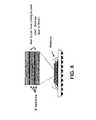
- FIG. 6is a view of a localized interconnect interface configured for connecting an integrated circuit to a second integrated circuit.
- FIG. 1illustrates a view of an integrated circuit assembly in accordance with an exemplary embodiment of the present invention.
- the integrated circuit assembly 100includes a substrate 102 .
- the substrate 102may be (or may be part of) a chip carrier, such as a Ball Grid Array, a Chip Scale Package substrate, a package substrate, a device substrate, a Ceramic Pin Grid Array (CPGA), a Dual in-line package, an Organic Pin Grid Array (OPGA), a Flip-chip Pin Grid Array, a Pin Grid Array, a Multi-chip Module (MCM), or the like, and may be configured for at least partially encapsulating and protecting an integrated circuit 104 .
- a chip carriersuch as a Ball Grid Array, a Chip Scale Package substrate, a package substrate, a device substrate, a Ceramic Pin Grid Array (CPGA), a Dual in-line package, an Organic Pin Grid Array (OPGA), a Flip-chip Pin Grid Array, a Pin Grid Array, a Multi-chip Module
- the substrate 102may form a recessed area which is at least partially guarded by an at least partial enclosure 114 configured for at least partially encapsulating an integrated circuit (ex.—die, chip) and protecting the integrated circuit 104 .
- the substrate 102may be formed of a ceramic material, a plastic material, an epoxy material or the like for promoting the prevention of physical damage and/or corrosion of the integrated circuit 104 .
- the substrate 102may be a printed circuit board.
- the printed circuit boardmay be a motherboard, an expansion board, a card, a daughtercard, a controller board, a network interface card (NIC), a video adapter, or the like.
- the integrated circuit assembly 100includes the integrated circuit 104 .
- the integrated circuit 104may be a microcircuit, a chip, a microchip, a silicon chip, a computer chip, a monolithic integrated circuit, a hybrid integrated circuit, or the like.
- the integrated circuit 104 of the present inventionis configured for being mounted to the substrate 102 via a localized interconnect interface 106 , the interface being configured for connecting (ex—electrically connecting) the integrated circuit to the substrate.
- the integrated circuit 104may be wire bonded (such as by ball bonding, wedge bonding, or the like) to the substrate 102 , with the localized interconnect interface 106 being a bond wire-bond pad interface.
- the bond wire-bond pad interfacemay include one or more bond wires 108 and/or bond pads 110 .
- a bond wire included in the one or more bond wires 108may be a gold, copper, or aluminum wire.
- a first end of the bond wire 108may be configured for attachment to an inner lead of the substrate 102
- a second end of the bond wire 108may be configured for attachment to a bond pad 110 of the integrated circuit 104 .
- one or more of heat, pressure and ultrasonic energymay be utilized in attaching the ends of the wire 108 to the substrate 102 and integrated circuit 104 respectively for electrically connecting to and/or securing the integrated circuit 104 onto the substrate.
- the integrated circuit 104 and the localized interconnect interface 106 of the integrated circuit assembly 100may be at least partially coated with a coating 112 .
- the coatingmay be applied at/over an attachment point between the bond wire 108 and the bond pad 110 of the integrated circuit 104 .
- the coating 112may be applied over a surface of a ball bond formed when the bond wire 108 is attached to the bond pad 110 , thereby covering the ball bond, at least part of the bond wire 108 and the bond pad 110 of the integrated circuit 104 .
- Corrosion at an interface between the ball bond 106 and/or the bond pad 110is a primary point of failure for a number of integrated circuit assemblies in harsh environments.
- the localized interconnect interfacemay be any areas, surfaces, etc. of the integrated circuit (ex—die attach) and the substrate 102 which may contact one another.
- the localized interconnect interfacemay be an attachment point between the bond wire 108 and the substrate 102 wherein the coating may also be applied.
- the localized interconnect interfacemay be configured for connecting the integrated circuit 104 to a second integrated circuit of the assembly 100 .
- the localized interconnect interfacemay be configured for connecting the bond pad 108 on the integrated circuit 104 to a bond pad located on the second integrated circuit.
- the localized interconnect interfacemay be configured for connecting the bond pad 110 of the integrated circuit 104 to a second bond pad on the same integrated circuit 104 .
- the localized interconnect interfacemay be a point (ex—area, surface, etc.) of attachment between a flip-chip bonded integrated circuit (ex—chip) and its corresponding substrate.
- the integrated circuit 104may be connected directly to a printed circuit board, with the coating being applied at an attachment point between the integrated circuit 104 and the printed circuit board.
- the coating 112may be a hermetic (ex—airtight) or near-hermetic coating for promoting reliability of the integrated circuit assembly 100 in high temperature operating environments and/or corrosive operating environments, such as military or avionics environments.
- the coating 112may be a low processing temperature coating.
- the coating 112may be formulated for being applied and/or cured at a temperature less than or equal to 160 degrees Celsius.
- the coating 112may be a glass-based Coating.
- the coatingmay be an alkali silicate-based coating.
- the coatingmay be a variety of formulations, such as any one or more of the formulations described in U.S. patent application Ser. No. 11/508,782 entitled: Integrated Circuit Protection and Ruggedization Coatings and Methods filed Aug. 23, 2006, (pending) which is herein incorporated by reference in its entirety.
- the integrated circuit 104may be a device which is available for at least one of sale, lease and license to a general public.
- the integrated circuit 104may be a Commercial off the Shelf (COTS) device.
- COTSCommercial off the Shelf
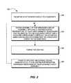
- FIG. 2illustrates a method for providing an integrated circuit assembly, the integrated circuit assembly including an integrated circuit and a substrate in accordance with an exemplary embodiment of the present invention.
- the method 200includes mounting the integrated circuit to the substrate 202 .
- the method 200further includes, during assembly of the integrated circuit assembly, applying a low processing temperature, at least near-hermetic, glass-based coating directly to the integrated circuit and a localized interconnect interface for the integrated circuit and the substrate 204 .
- the localized interconnect interfacemay be a bond wire-bond pad interface as discussed above.
- the glass-based coatingmay be an alkali silicate-based coating.
- the method 200further includes curing the coating 206 .
- the steps of applying the coating 204 and curing the coating 206may be performed at a temperature less than or equal to 160 degrees Celsius.
- applying the coating 204may include applying the coating in one or more layers, which may promote prevention of cracking of the coating during curing.
- the coatingmay be maintained/stored and/or applied at atmospheric pressure.
- the method 200further includes, prior to applying the coating, adding nanoparticles/nano-sized particles (ex—particles having at least one dimension less than 100 nm) to the coating for promoting corrosion resistance of the assembly 208 and/or the coating itself.
- nanoparticles/nano-sized particlesex—particles having at least one dimension less than 100 nm
- nano-sized particles of calcium carbonate, zinc oxide, divalent metal cations, rare earth oxides and/or the likemay be added to the coating for promoting corrosion resistance of the integrated circuit assembly.
- FIG. 3illustrates a method for providing an electronic device, the electronic device including an integrated circuit assembly, the integrated circuit assembly including an integrated circuit and a substrate in accordance with an exemplary embodiment of the present invention.
- the electronic devicemay be a computer, a cellular phone, or various other devices which may implement the integrated circuit assembly.
- the method 300includes mounting the integrated circuit to the substrate 302 .
- the method 300further includes, during assembly of the integrated circuit assembly, applying a low processing temperature, at least near-hermetic, glass-based coating directly to the integrated circuit and a localized interconnect interface for the integrated circuit and the substrate 304 .
- the localized interconnect interfacemay be a bond wire-bond pad interface as discussed above.
- the glass-based coatingmay be an alkali silicate-based coating.
- the method 300further includes curing the coating 306 .
- the steps of applying the coating 304 and curing the coating 306may be performed at a temperature lower than 160 degrees Celsius.
- applying the coating 304may include applying the coating in one or more layers, which may promote prevention of cracking of the coating during curing.
- the method 300further includes at least substantially enclosing the integrated circuit assembly within a housing 308 .
- the electronic device 500may be a computer and the housing 502 may be a computer tower.
- the step of enclosing the integrated circuit assembly within the housing 308may include mounting the integrated circuit assembly (ex—integrated circuit and chip carrier) to a printed circuit board, then at least substantially enclosing the integrated circuit assembly and printed circuit board within the housing.
- the printed circuit boardmay be a motherboard, an expansion board, a card, a daughtercard, a controller board, a network interface card (NIC), a video adapter, or the like.
- NICnetwork interface card
- the method 300further includes, prior to applying the coating, adding nanoparticles/nano-sized particles (ex—particles having at least one dimension less than 100 nm) to the coating for promoting corrosion resistance of the assembly 310 and/or the coating itself.
- nanoparticles/nano-sized particlesex—particles having at least one dimension less than 100 nm
- nano-sized particles of calcium carbonate, zinc oxide, and/or the likemay be added to the coating for promoting corrosion resistance of the integrated circuit assembly.
- Such a software packagemay be a computer program product which employs a computer-readable storage medium including stored computer code which is used to program a computer to perform the disclosed function and process of the present invention.
- the computer-readable mediummay include, but is not limited to, any type of conventional floppy disk, optical disk, CD-ROM, magnetic disk, hard disk drive, magneto-optical disk, ROM, RAM, EPROM, EEPROM, magnetic or optical card, or any other suitable media for storing electronic instructions.
Landscapes
- Engineering & Computer Science (AREA)
- Microelectronics & Electronic Packaging (AREA)
- Power Engineering (AREA)
- Computer Hardware Design (AREA)
- Chemical & Material Sciences (AREA)
- Condensed Matter Physics & Semiconductors (AREA)
- General Physics & Mathematics (AREA)
- Physics & Mathematics (AREA)
- Ceramic Engineering (AREA)
- Dispersion Chemistry (AREA)
- Materials Engineering (AREA)
- Manufacturing & Machinery (AREA)
- Structures Or Materials For Encapsulating Or Coating Semiconductor Devices Or Solid State Devices (AREA)
- Non-Metallic Protective Coatings For Printed Circuits (AREA)
Abstract
Description
The present application is a continuation-in-part application and claims priority under 35 U.S.C. §120 to the U.S. patent application Ser. No. 11/508,782 entitled: Integrated Circuit Protection and Ruggedization Coatings and Methods filed Aug. 23, 2006 now U.S. Pat. No. 8,076,185, which is herein incorporated by reference in its entirety.
The present invention relates to the field of packaging and interconnection of integrated circuit assemblies and particularly to a method for providing near-hermetically coated integrated circuit assemblies.
Integrated circuit packages are produced for usage in a variety of products or for a variety of applications. For example, integrated circuit packages which are designed for use in military and avionics applications are often required to survive and/or operate under aggressive or rigorous operating conditions and environments. These integrated circuit packages (ex—hermetic packages) are often expected to have a long lifespan (i.e., remain functionally operable over a long period of time), such as for 20 years or more, and are typically very costly to produce.
Contrastingly, most currently available integrated circuit packages are designed for usage in products which present relatively benign/much less rigorous operating conditions, such as desktop PC's, electronic games and cell phones. Such integrated circuit packages are commonly referred to as Commercial off the Shelf (COTS) devices. These COTS devices tend to have a relatively short lifespan (ex—2 to 5 years) and are relatively inexpensive to produce compared to military electronics components.
In recent years the military electronics industry has sought a less expensive alternative to the high cost integrated circuit packages discussed above, which are currently implemented in environmentally severe military and avionics applications. One alternative has been to implement the currently available (and less expensive) COTS devices, in the more demanding military and avionics environments. However, when the currently available COTS devices have been subjected to these more rigorous conditions, they have been especially prone to failure due to higher operating temperatures, corrosion, or the like. Current methods of modifying or designing integrated circuit packages for improved corrosion resistance are typically very expensive and may exacerbate other failure mechanisms and thereby reduce reliability.
Thus, it would be desirable to have a method for providing near-hermetically coated integrated circuit assemblies which address the problems associated with current solutions.
Accordingly, an embodiment of the present invention is directed to a method for providing an integrated circuit assembly, the integrated circuit assembly including an integrated circuit and a substrate, the method including: mounting the integrated circuit to the substrate; during assembly of the integrated circuit assembly, applying a low processing temperature, at least near-hermetic, glass-based coating directly to the integrated circuit and a localized interconnect interface, the interface being configured for connecting the integrated circuit to at least one of the substrate and a second integrated circuit of the assembly; and curing the coating.
A further embodiment of the present invention is directed to a method for providing an electronic device, the electronic device including an integrated circuit assembly, the integrated circuit assembly including an integrated circuit and a substrate, the method including: mounting the integrated circuit to the substrate; during assembly of the integrated circuit assembly, applying a low processing temperature, at least near-hermetic, glass-based coating directly to the integrated circuit and a localized interconnect interface, the interface being configured for connecting the integrated circuit to at least one of the substrate and a second integrated circuit of the assembly; curing the coating; and at least substantially enclosing the integrated circuit assembly within a housing.
A still further embodiment of the present invention is directed to an integrated circuit assembly, including: a substrate; and an integrated circuit configured for being mounted to the substrate via a localized interconnect interface, the interface being configured for connecting the integrated circuit to at least one of the substrate and a second integrated circuit of the assembly, wherein the integrated circuit and the localized interconnect interface are at least partially coated with a low processing temperature, at least near-hermetic, glass-based coating for promoting reliability of the integrated circuit assembly in at least one of high temperature operating environments and corrosive operating environments.
The numerous advantages of the present invention may be better understood by those skilled in the art by reference to the accompanying figures in which:
Reference will now be made in detail to the presently preferred embodiments of the invention, examples of which are illustrated in the accompanying drawings.
In current embodiments, theintegrated circuit assembly 100 includes theintegrated circuit 104. For instance, the integrated circuit104 (IC) may be a microcircuit, a chip, a microchip, a silicon chip, a computer chip, a monolithic integrated circuit, a hybrid integrated circuit, or the like.
Theintegrated circuit 104 of the present invention is configured for being mounted to thesubstrate 102 via a localizedinterconnect interface 106, the interface being configured for connecting (ex—electrically connecting) the integrated circuit to the substrate. For example, theintegrated circuit 104 may be wire bonded (such as by ball bonding, wedge bonding, or the like) to thesubstrate 102, with the localizedinterconnect interface 106 being a bond wire-bond pad interface. Further, the bond wire-bond pad interface may include one ormore bond wires 108 and/orbond pads 110. For instance, a bond wire included in the one ormore bond wires 108 may be a gold, copper, or aluminum wire. Further, a first end of thebond wire 108 may be configured for attachment to an inner lead of thesubstrate 102, while a second end of thebond wire 108 may be configured for attachment to abond pad 110 of theintegrated circuit 104. For example, one or more of heat, pressure and ultrasonic energy may be utilized in attaching the ends of thewire 108 to thesubstrate 102 and integratedcircuit 104 respectively for electrically connecting to and/or securing theintegrated circuit 104 onto the substrate.
In an exemplary embodiment, theintegrated circuit 104 and the localizedinterconnect interface 106 of the integrated circuit assembly100 (shown prior to being coated/without coating inFIG. 4A ) may be at least partially coated with acoating 112. (as shown inFIG. 4B in accordance with configurations of the present invention). For example, as shown inFIG. 4B , the coating may be applied at/over an attachment point between thebond wire 108 and thebond pad 110 of the integratedcircuit 104. For instance, thecoating 112 may be applied over a surface of a ball bond formed when thebond wire 108 is attached to thebond pad 110, thereby covering the ball bond, at least part of thebond wire 108 and thebond pad 110 of theintegrated circuit 104. Corrosion at an interface between theball bond 106 and/or thebond pad 110 is a primary point of failure for a number of integrated circuit assemblies in harsh environments. In further embodiments, the localized interconnect interface may be any areas, surfaces, etc. of the integrated circuit (ex—die attach) and thesubstrate 102 which may contact one another. In additional embodiments, the localized interconnect interface may be an attachment point between thebond wire 108 and thesubstrate 102 wherein the coating may also be applied. Further, the localized interconnect interface may be configured for connecting theintegrated circuit 104 to a second integrated circuit of theassembly 100. For example, the localized interconnect interface may be configured for connecting thebond pad 108 on theintegrated circuit 104 to a bond pad located on the second integrated circuit. Alternatively, the localized interconnect interface may be configured for connecting thebond pad 110 of theintegrated circuit 104 to a second bond pad on the sameintegrated circuit 104. In further embodiments, the localized interconnect interface may be a point (ex—area, surface, etc.) of attachment between a flip-chip bonded integrated circuit (ex—chip) and its corresponding substrate. In alternative embodiments, theintegrated circuit 104 may be connected directly to a printed circuit board, with the coating being applied at an attachment point between theintegrated circuit 104 and the printed circuit board.
In a current embodiment, thecoating 112 may be a hermetic (ex—airtight) or near-hermetic coating for promoting reliability of the integratedcircuit assembly 100 in high temperature operating environments and/or corrosive operating environments, such as military or avionics environments. In further embodiments, thecoating 112 may be a low processing temperature coating. For instance, thecoating 112 may be formulated for being applied and/or cured at a temperature less than or equal to 160 degrees Celsius. In additional embodiments, thecoating 112 may be a glass-based Coating. For example, the coating may be an alkali silicate-based coating. Still further, the coating may be a variety of formulations, such as any one or more of the formulations described in U.S. patent application Ser. No. 11/508,782 entitled: Integrated Circuit Protection and Ruggedization Coatings and Methods filed Aug. 23, 2006, (pending) which is herein incorporated by reference in its entirety.
In a present embodiment, theintegrated circuit 104 may be a device which is available for at least one of sale, lease and license to a general public. For instance, theintegrated circuit 104 may be a Commercial off the Shelf (COTS) device.
In a present embodiment, themethod 200 further includes, prior to applying the coating, adding nanoparticles/nano-sized particles (ex—particles having at least one dimension less than 100 nm) to the coating for promoting corrosion resistance of theassembly 208 and/or the coating itself. For example, nano-sized particles of calcium carbonate, zinc oxide, divalent metal cations, rare earth oxides and/or the like may be added to the coating for promoting corrosion resistance of the integrated circuit assembly.
In further embodiments, themethod 300 further includes at least substantially enclosing the integrated circuit assembly within ahousing 308. For example, as shown inFIG. 5 , theelectronic device 500 may be a computer and thehousing 502 may be a computer tower. In embodiments where the substrate is, for instance, a chip carrier, the step of enclosing the integrated circuit assembly within thehousing 308, may include mounting the integrated circuit assembly (ex—integrated circuit and chip carrier) to a printed circuit board, then at least substantially enclosing the integrated circuit assembly and printed circuit board within the housing. For example, the printed circuit board may be a motherboard, an expansion board, a card, a daughtercard, a controller board, a network interface card (NIC), a video adapter, or the like.
In present embodiments, themethod 300 further includes, prior to applying the coating, adding nanoparticles/nano-sized particles (ex—particles having at least one dimension less than 100 nm) to the coating for promoting corrosion resistance of theassembly 310 and/or the coating itself. For example, nano-sized particles of calcium carbonate, zinc oxide, and/or the like may be added to the coating for promoting corrosion resistance of the integrated circuit assembly.
It is to be noted that the foregoing described embodiments according to the present invention may be conveniently implemented using conventional general purpose digital computers programmed according to the teachings of the present specification, as will be apparent to those skilled in the computer art. Appropriate software coding may readily be prepared by skilled programmers based on the teachings of the present disclosure, as will be apparent to those skilled in the software art.
It is to be understood that the present invention may be conveniently implemented in forms of a software package. Such a software package may be a computer program product which employs a computer-readable storage medium including stored computer code which is used to program a computer to perform the disclosed function and process of the present invention. The computer-readable medium may include, but is not limited to, any type of conventional floppy disk, optical disk, CD-ROM, magnetic disk, hard disk drive, magneto-optical disk, ROM, RAM, EPROM, EEPROM, magnetic or optical card, or any other suitable media for storing electronic instructions.
It is understood that the specific order or hierarchy of steps in the foregoing disclosed methods are examples of exemplary approaches. Based upon design preferences, it is understood that the specific order or hierarchy of steps in the method can be rearranged while remaining within the scope of the present invention. The accompanying method claims present elements of the various steps in a sample order, and are not meant to be limited to the specific order or hierarchy presented.
It is believed that the present invention and many of its attendant advantages will be understood by the foregoing description. It is also believed that it will be apparent that various changes may be made in the form, construction and arrangement of the components thereof without departing from the scope and spirit of the invention or without sacrificing all of its material advantages. The form herein before described being merely an explanatory embodiment thereof, it is the intention of the following claims to encompass and include such changes.
Claims (18)
1. An integrated circuit assembly, comprising:
a substrate; and
an integrated circuit configured for being mounted to the substrate and comprising a localized interconnect interface, the interface being configured for connecting the integrated circuit to at least one of the substrate and a second integrated circuit of the assembly,
wherein the integrated circuit and the localized interconnect interface are at least partially coated with an alkali silicate glass coating for promoting reliability of the integrated circuit assembly in at least one of high temperature operating environments and corrosive operating environments; and
wherein the alkali silicate glass-based coating is produced from alkali metal oxide and silicon dioxide.
2. An integrated circuit assembly as claimed inclaim 1 , wherein the substrate is a chip carrier.
3. An integrated circuit assembly as claimed inclaim 1 , wherein the localized interconnect interface is a bond wire-bond pad interface, the bond wire-bond pad interface including at least one of a bond wire and a bond pad.
4. An integrated circuit assembly as claimed inclaim 1 , wherein the integrated circuit is a Commercial off the Shelf (COTS) device.
5. An integrated circuit assembly as claimed inclaim 1 , wherein the substrate is a printed circuit board.
6. An integrated circuit assembly, comprising:
a substrate;
an integrated circuit coupled to the substrate;
an interconnect interface configured to couple the integrated circuit to at least one of the substrate and a second integrated circuit of the assembly,
wherein the integrated circuit and the interconnect interface are at least partially coated with a low processing temperature, at least near-hermetic, glass-based coating for promoting reliability of the integrated circuit assembly in at least one of high temperature operating environments and corrosive operating environments, wherein the glass-based coating is an alkali silicate glass-based coating; and
wherein the alkali silicate glass-based coating is produced from alkali metal oxide and silicon dioxide.
7. The integrated circuit assembly ofclaim 6 , wherein the substrate is a chip carrier or printed circuit board.
8. The integrated circuit assembly ofclaim 7 , wherein the integrated circuit comprises a chip.
9. The integrated circuit assembly ofclaim 8 , wherein the interconnect interface comprises a bond wire-bond pad interface.
10. The integrated circuit assembly ofclaim 9 , wherein the integrated circuit is a flip-chip bonded integrated circuit.
11. The integrated circuit assembly ofclaim 8 , wherein the interconnect interface is configured to couple the integrated circuit to the second integrated circuit of the assembly.
12. The integrated circuit assembly ofclaim 8 , wherein the alkali silicate glass-based coating is formulated for being applied and cured at a temperature less than or equal to 160 degrees Celsius.
13. The integrated circuit assembly ofclaim 12 , wherein the alkali silicate glass-based coating comprises a plurality of layers.
14. The integrated circuit assembly ofclaim 13 , wherein the alkali silicate glass-based coating comprises nanoparticles selected from the group consisting of calcium carbonate, zinc oxide, divalent metal cations and rare earth oxides.
15. An electronic device, comprising:
an integrated circuit assembly; and
a housing substantially enclosing the integrated circuit assembly, wherein the integrated circuit assembly comprises:
a substrate;
an integrated circuit coupled to the substrate;
an interconnect interface configured to couple the integrated circuit to at least one of the substrate and a second integrated circuit of the assembly,
wherein the integrated circuit and the interconnect interface are at least partially coated with a low processing temperature, at least near-hermetic, glass-based coating for promoting reliability of the integrated circuit assembly in at least one of high temperature operating environments and corrosive operating environments, wherein the glass-based coating is an alkali silicate glass-based coating; and
wherein the alkali silicate glass-based coating is produced from M2O and SiO2, wherein M is an alkali metal.
16. The electronic device ofclaim 15 , wherein the electronic device is a cellular phone.
17. The electronic device ofclaim 15 , wherein the substrate comprises a printed circuit board, wherein the printed circuit board is selected from the group consisting of a network interface card, a video adapter, and a motherboard.
18. The electronic device ofclaim 15 , wherein the housing is a computer tower.
Priority Applications (4)
| Application Number | Priority Date | Filing Date | Title |
|---|---|---|---|
| US11/732,982US8581108B1 (en) | 2006-08-23 | 2007-04-05 | Method for providing near-hermetically coated integrated circuit assemblies |
| US12/240,775US8617913B2 (en) | 2006-08-23 | 2008-09-29 | Alkali silicate glass based coating and method for applying |
| US14/055,746US8935848B1 (en) | 2006-08-23 | 2013-10-16 | Method for providing near-hermetically coated integrated circuit assemblies |
| US14/140,192US9565758B2 (en) | 2006-08-23 | 2013-12-24 | Alkali silicate glass based coating and method for applying |
Applications Claiming Priority (2)
| Application Number | Priority Date | Filing Date | Title |
|---|---|---|---|
| US11/508,782US8076185B1 (en) | 2006-08-23 | 2006-08-23 | Integrated circuit protection and ruggedization coatings and methods |
| US11/732,982US8581108B1 (en) | 2006-08-23 | 2007-04-05 | Method for providing near-hermetically coated integrated circuit assemblies |
Related Parent Applications (3)
| Application Number | Title | Priority Date | Filing Date |
|---|---|---|---|
| US11/508,782Continuation-In-PartUS8076185B1 (en) | 2006-08-23 | 2006-08-23 | Integrated circuit protection and ruggedization coatings and methods |
| US11/732,981Continuation-In-PartUS8166645B2 (en) | 2006-08-23 | 2007-04-05 | Method for providing near-hermetically coated, thermally protected integrated circuit assemblies |
| US11/784,158Continuation-In-PartUS7915527B1 (en) | 2006-08-23 | 2007-04-05 | Hermetic seal and hermetic connector reinforcement and repair with low temperature glass coatings |
Related Child Applications (3)
| Application Number | Title | Priority Date | Filing Date |
|---|---|---|---|
| US11/732,981Continuation-In-PartUS8166645B2 (en) | 2006-08-23 | 2007-04-05 | Method for providing near-hermetically coated, thermally protected integrated circuit assemblies |
| US11/784,158Continuation-In-PartUS7915527B1 (en) | 2006-08-23 | 2007-04-05 | Hermetic seal and hermetic connector reinforcement and repair with low temperature glass coatings |
| US14/055,746DivisionUS8935848B1 (en) | 2006-08-23 | 2013-10-16 | Method for providing near-hermetically coated integrated circuit assemblies |
Publications (1)
| Publication Number | Publication Date |
|---|---|
| US8581108B1true US8581108B1 (en) | 2013-11-12 |
Family
ID=49518028
Family Applications (2)
| Application Number | Title | Priority Date | Filing Date |
|---|---|---|---|
| US11/732,982Active2029-10-08US8581108B1 (en) | 2006-08-23 | 2007-04-05 | Method for providing near-hermetically coated integrated circuit assemblies |
| US14/055,746ActiveUS8935848B1 (en) | 2006-08-23 | 2013-10-16 | Method for providing near-hermetically coated integrated circuit assemblies |
Family Applications After (1)
| Application Number | Title | Priority Date | Filing Date |
|---|---|---|---|
| US14/055,746ActiveUS8935848B1 (en) | 2006-08-23 | 2013-10-16 | Method for providing near-hermetically coated integrated circuit assemblies |
Country Status (1)
| Country | Link |
|---|---|
| US (2) | US8581108B1 (en) |
Cited By (10)
| Publication number | Priority date | Publication date | Assignee | Title |
|---|---|---|---|---|
| US8935848B1 (en)* | 2006-08-23 | 2015-01-20 | Rockwell Collins, Inc. | Method for providing near-hermetically coated integrated circuit assemblies |
| US9197024B1 (en) | 2006-08-23 | 2015-11-24 | Rockwell Collins, Inc. | Method of reinforcing a hermetic seal of a module |
| US9196555B1 (en) | 2006-08-23 | 2015-11-24 | Rockwell Collins, Inc. | Integrated circuit protection and ruggedization coatings and methods |
| US9565758B2 (en) | 2006-08-23 | 2017-02-07 | Rockwell Collins, Inc. | Alkali silicate glass based coating and method for applying |
| US11499234B2 (en) | 2019-03-11 | 2022-11-15 | Massachusetts Institute Of Technology | Liquid low temperature oxide |
| US11610846B2 (en)* | 2019-04-12 | 2023-03-21 | Adeia Semiconductor Bonding Technologies Inc. | Protective elements for bonded structures including an obstructive element |
| US11728287B2 (en) | 2019-04-12 | 2023-08-15 | Adeia Semiconductor Bonding Technologies Inc. | Wafer-level bonding of obstructive elements |
| US11848284B2 (en) | 2019-04-12 | 2023-12-19 | Adeia Semiconductor Bonding Technologies Inc. | Protective elements for bonded structures |
| US12174246B2 (en) | 2019-05-23 | 2024-12-24 | Adeia Semiconductor Bonding Technologies Inc. | Security circuitry for bonded structures |
| US12300634B2 (en) | 2021-08-02 | 2025-05-13 | Adeia Semiconductor Bonding Technologies Inc. | Protective semiconductor elements for bonded structures |
Citations (136)
| Publication number | Priority date | Publication date | Assignee | Title |
|---|---|---|---|---|
| US3508974A (en) | 1964-11-12 | 1970-04-28 | Reinhard G Bressler | Thermoelectric device with fluid thermoelectric element |
| US3654528A (en) | 1970-08-03 | 1972-04-04 | Gen Electric | Cooling scheme for a high-current semiconductor device employing electromagnetically-pumped liquid metal for heat and current transfer |
| US3723790A (en) | 1971-02-01 | 1973-03-27 | Corning Glass Works | Electrical lamp or tube comprising copper coated nickel-iron alloy electrical current conductors and a glass enclosure |
| US3812404A (en) | 1973-05-29 | 1974-05-21 | Gen Electric | Increasing the initial flow rate in a rectifier assembly employing electromagnetically-pumped liquid metal for cooling |
| US4177015A (en) | 1977-03-23 | 1979-12-04 | United Kingdom Atomic Energy Authority | Electromagnetic pumps |
| US4294658A (en) | 1978-10-09 | 1981-10-13 | United Kingdom Atomic Energy Authority | Nuclear reactors |
| US4410874A (en) | 1975-03-03 | 1983-10-18 | Hughes Aircraft Company | Large area hybrid microcircuit assembly |
| US4505644A (en) | 1982-12-06 | 1985-03-19 | The United States Of America As Represented By The United States Department Of Energy | Linear induction pump |
| US4513029A (en) | 1982-07-16 | 1985-04-23 | Osaka Suda Co. Ltd. | Sea water antifouling method |
| US4560084A (en) | 1981-09-02 | 1985-12-24 | Burr-Brown Corporation | Heater preform for sealing a closure |
| US4572924A (en) | 1983-05-18 | 1986-02-25 | Spectrum Ceramics, Inc. | Electronic enclosures having metal parts |
| US4622433A (en) | 1984-03-30 | 1986-11-11 | Diacon, Inc. | Ceramic package system using low temperature sealing glasses |
| US4761518A (en) | 1987-01-20 | 1988-08-02 | Olin Corporation | Ceramic-glass-metal packaging for electronic components incorporating unique leadframe designs |
| US4765948A (en) | 1986-08-29 | 1988-08-23 | Stone & Webster Engineering Corporation | Coolant circulation system for a liquid metal nuclear reactor |
| US4773826A (en) | 1982-02-10 | 1988-09-27 | Westinghouse Electric Corp. | Pump |
| US4802531A (en) | 1986-06-17 | 1989-02-07 | Electric Power Research Institute | Pump/intermediate heat exchanger assembly for a liquid metal reactor |
| US4882212A (en) | 1986-10-30 | 1989-11-21 | Olin Corporation | Electronic packaging of components incorporating a ceramic-glass-metal composite |
| US4963503A (en) | 1984-04-09 | 1990-10-16 | Hosiden Electronics Co., Ltd. | Method of manufacturing liquid crystal display device |
| US5041342A (en) | 1988-07-08 | 1991-08-20 | Ngk Insulators, Ltd. | Multilayered ceramic substrate fireable in low temperature |
| US5136365A (en) | 1990-09-27 | 1992-08-04 | Motorola, Inc. | Anisotropic conductive adhesive and encapsulant material |
| US5140109A (en) | 1989-08-25 | 1992-08-18 | Kyocera Corporation | Container package for semiconductor element |
| US5184211A (en) | 1988-03-01 | 1993-02-02 | Digital Equipment Corporation | Apparatus for packaging and cooling integrated circuit chips |
| US5195231A (en) | 1992-02-18 | 1993-03-23 | General Electric Company | Method for producing inner stators for electromagnetic pumps |
| US5232970A (en) | 1990-08-31 | 1993-08-03 | The Dow Chemical Company | Ceramic-filled thermally-conductive-composites containing fusible semi-crystalline polyamide and/or polybenzocyclobutenes for use in microelectronic applications |
| US5244726A (en) | 1988-02-23 | 1993-09-14 | The Hera Corporation | Advanced geopolymer composites |
| US5265136A (en) | 1991-10-01 | 1993-11-23 | Kabushiki Kaisha Toshiba | Sodium cooled fast reactor |
| US5288769A (en) | 1991-03-27 | 1994-02-22 | Motorola, Inc. | Thermally conducting adhesive containing aluminum nitride |
| US5315155A (en) | 1992-07-13 | 1994-05-24 | Olin Corporation | Electronic package with stress relief channel |
| US5405808A (en) | 1993-08-16 | 1995-04-11 | Lsi Logic Corporation | Fluid-filled and gas-filled semiconductor packages |
| US5502889A (en) | 1988-06-10 | 1996-04-02 | Sheldahl, Inc. | Method for electrically and mechanically connecting at least two conductive layers |
| US5581286A (en) | 1991-12-31 | 1996-12-03 | Compaq Computer Corporation | Multi-channel array actuation system for an ink jet printhead |
| US5686703A (en) | 1994-12-16 | 1997-11-11 | Minnesota Mining And Manufacturing Company | Anisotropic, electrically conductive adhesive film |
| US5690837A (en) | 1995-05-23 | 1997-11-25 | Hitachi Chemical Company, Ltd. | Process for producing multilayer printed circuit board |
| US5702963A (en) | 1990-12-31 | 1997-12-30 | Kopin Corporation | Method of forming high density electronic circuit modules |
| US5863605A (en) | 1996-03-18 | 1999-01-26 | Celestech, Inc. | Diamond film deposition |
| US5916944A (en)* | 1993-03-08 | 1999-06-29 | Dow Corning Corporation | Tamper-proof electronic coatings |
| US5958794A (en) | 1995-09-22 | 1999-09-28 | Minnesota Mining And Manufacturing Company | Method of modifying an exposed surface of a semiconductor wafer |
| US5965947A (en) | 1996-08-20 | 1999-10-12 | Samsung Electronics Co., Ltd. | Structure of a semiconductor package including chips bonded to die bonding pad with conductive adhesive and chips bonded with non-conductive adhesive containing insulating beads |
| US5991351A (en) | 1998-09-22 | 1999-11-23 | U.S. Department Of Energy | Method and system to directly produce electrical power within the lithium blanket region of a magnetically confined, deuterium-tritium (DT) fueled, thermonuclear fusion reactor |
| US6010956A (en) | 1996-02-29 | 2000-01-04 | Tokyo Ohka Kogyo Co., Ltd. | Process for producing multilayer wiring boards |
| US6019165A (en) | 1998-05-18 | 2000-02-01 | Batchelder; John Samuel | Heat exchange apparatus |
| US6021844A (en) | 1998-06-03 | 2000-02-08 | Batchelder; John Samuel | Heat exchange apparatus |
| US6028619A (en)* | 1997-10-06 | 2000-02-22 | Seiko Instruments Inc. | Thermal head |
| US6027791A (en)* | 1996-09-30 | 2000-02-22 | Kyocera Corporation | Structure for mounting a wiring board |
| US6039896A (en) | 1998-03-18 | 2000-03-21 | Sumitomo Bakelite Co., Ltd. | Anisotropic conductive adhesive and method for preparation thereof and an electronic apparatus using said adhesive |
| US6048656A (en) | 1999-05-11 | 2000-04-11 | Micron Technology, Inc. | Void-free underfill of surface mounted chips |
| US6087018A (en) | 1997-01-14 | 2000-07-11 | Seiko Epson Corporation | Method for surface treatment, ornaments and electronic devices |
| US6110656A (en) | 1998-09-28 | 2000-08-29 | Eastman Kodak Company | Colloidal vanadium oxide having improved stability |
| US6121175A (en)* | 1997-06-12 | 2000-09-19 | Ivoclar Ag | Alkali silicate glass |
| US6124224A (en) | 1998-09-02 | 2000-09-26 | Ferro Corporation | High temperature sealing glass |
| US6159910A (en) | 1998-02-06 | 2000-12-12 | Shin-Etsu Chemical Co., Ltd. | Aluminum nitride composition |
| US20010015443A1 (en) | 1998-05-27 | 2001-08-23 | Satoshi Komoto | Semiconductor light emitting device |
| US20010046933A1 (en) | 2000-02-07 | 2001-11-29 | Parkhill Robert L. | Sol-gel-based composite materials for direct-write electronics applications |
| US20020000630A1 (en)* | 2000-01-31 | 2002-01-03 | Coyle Anthony L. | Plastic package for micromechanical devices |
| US6356334B1 (en) | 1998-08-06 | 2002-03-12 | National Semiconductor Corporation | Liquid crystal display assembly and method for reducing residual stresses |
| US6370015B2 (en)* | 2000-03-17 | 2002-04-09 | Murata Manufacturing Co., Ltd. | Laminated ceramic electronic device |
| US20020054976A1 (en) | 2000-07-21 | 2002-05-09 | Shoji Nakamura | Molded glass substrate for magnetic disk and method for manufacturing the same |
| US20020076192A1 (en) | 1997-09-24 | 2002-06-20 | Bartholomew Roger F. | Rare earth doped optical glasses |
| US20020078856A1 (en) | 1997-01-31 | 2002-06-27 | John Hahn | Corrosion protective coatings |
| US20020086115A1 (en) | 2000-09-22 | 2002-07-04 | Lamers Paul H. | Curable polyurethanes, coatings prepared therefrom, and method of making the same |
| US6423415B1 (en) | 2000-08-31 | 2002-07-23 | Corning Incorporated | Potassium silicate frits for coating metals |
| US6451283B1 (en) | 2000-03-23 | 2002-09-17 | Engelhard Corporation | Macroscopic aggregates of microcrystalline zeolites |
| US6452090B2 (en) | 2000-01-19 | 2002-09-17 | Agency Of Industrial Science & Technology, Ministry Of International Trade & Industry | Photovoltaic device |
| US20020170173A1 (en) | 2001-05-21 | 2002-11-21 | Shinko Electric Industries Co., Ltd. | Method of production of circuit board, semiconductor device, and plating system |
| US6486087B1 (en) | 1999-09-17 | 2002-11-26 | Xcellsis Gmbh | Method for periodically reactivating a copper-containing catalyst material |
| US6496359B2 (en) | 2000-12-08 | 2002-12-17 | Sun Microsystems, Inc. | Tile array computers |
| US20020189495A1 (en) | 2001-03-26 | 2002-12-19 | Jsr Corporation | Composition for film formation, method of film formation, and silica-based film |
| US20020189894A1 (en) | 2001-06-13 | 2002-12-19 | Dikat, L.L.C. | Aural feedback apparatus |
| US20030047735A1 (en) | 2001-06-28 | 2003-03-13 | Takeshi Kyoda | Photoelectric conversion device, glass composition for coating silicon, and insulating coating in contact with silicon |
| US6541083B1 (en) | 2000-01-11 | 2003-04-01 | Guardian Industries Corp. | Vacuum IG unit with alkali silicate edge seal and/or spacers |
| US20030080341A1 (en) | 2001-01-24 | 2003-05-01 | Kensho Sakano | Light emitting diode, optical semiconductor element and epoxy resin composition suitable for optical semiconductor element and production methods therefor |
| US6586087B2 (en) | 1999-12-30 | 2003-07-01 | Corning Incorporated | Articles sealed with glass |
| US6599643B2 (en) | 1997-01-31 | 2003-07-29 | Elisha Holding Llc | Energy enhanced process for treating a conductive surface and products formed thereby |
| JP2003332505A (en) | 2002-05-15 | 2003-11-21 | Fujitsu Ltd | Cooling structure and heat transfer member |
| US20030218258A1 (en) | 2002-05-23 | 2003-11-27 | 3M Innovative Properties Company | Nanoparticle filled underfill |
| US6658861B1 (en) | 2002-12-06 | 2003-12-09 | Nanocoolers, Inc. | Cooling of high power density devices by electrically conducting fluids |
| US20030228424A1 (en) | 2002-03-06 | 2003-12-11 | Dove Clive Nicholas | Water borne coating composition for film transfer and casting process |
| US6665186B1 (en) | 2002-10-24 | 2003-12-16 | International Business Machines Corporation | Liquid metal thermal interface for an electronic module |
| US6708501B1 (en) | 2002-12-06 | 2004-03-23 | Nanocoolers, Inc. | Cooling of electronics by electrically conducting fluids |
| US20040106037A1 (en) | 2002-11-02 | 2004-06-03 | Samsung Sdi Co., Ltd. | Separator having inorganic protective film and lithium battery using the same |
| US20040116577A1 (en) | 2001-04-17 | 2004-06-17 | Tohru Naruse | Coating material composition having photocatalytic activity |
| US20040156995A1 (en) | 2001-08-17 | 2004-08-12 | Shinobu Komiyama | Treating agent for forming a protective coating and metallic materials with a protective coating |
| US6798072B2 (en) | 2000-11-10 | 2004-09-28 | Hitachi, Ltd. | Flip chip assembly structure for semiconductor device and method of assembling therefor |
| US6800326B1 (en) | 1997-01-14 | 2004-10-05 | Seiko Epson Corporation | Method of treating a surface of a surface of a substrate containing titanium for an ornament |
| US20040194667A1 (en) | 2002-04-10 | 2004-10-07 | Reuscher Craig J. | Solution for sealing porous metal substrates and process of applying the solution |
| US20050003947A1 (en) | 2000-09-20 | 2005-01-06 | Goodrich Corporation | Inorganic matrix compositions and composites incorporating the matrix composition |
| US20050082691A1 (en) | 2003-10-16 | 2005-04-21 | Nitto Denko Corporation | Epoxy resin composition for encapsulating optical semiconductor element and optical semiconductor device using the same |
| US20050099775A1 (en) | 2003-11-12 | 2005-05-12 | Himanshu Pokharna | Pumped liquid cooling for computer systems using liquid metal coolant |
| US20050116237A1 (en) | 2002-07-11 | 2005-06-02 | Sharp Laboratories Of America, Inc. | Method for forming a flexible metal foil substrate display |
| US20050123684A1 (en) | 2003-11-21 | 2005-06-09 | Makowski Michael P. | Coatings with improved chip resistance and methods of making the same |
| US6918984B2 (en) | 2002-06-24 | 2005-07-19 | Loctite (R&D) Limited | Photocurable adhesive compositions, reaction products of which have low halide ion content |
| US20050179742A1 (en) | 2004-01-29 | 2005-08-18 | Hewlett-Packard Development Company, L.P. | Method of making an inkjet printhead |
| JP2006045420A (en) | 2004-08-06 | 2006-02-16 | Tanaka Masataka | Coating composition and coated film obtained by the same |
| US20060045755A1 (en) | 2004-08-24 | 2006-03-02 | Dell Products L.P. | Information handling system including AC electromagnetic pump cooling apparatus |
| US20060068218A1 (en) | 2004-09-28 | 2006-03-30 | Hooghan Kultaransingh N | Whisker-free lead frames |
| US20060095677A1 (en) | 2004-08-17 | 2006-05-04 | Hakura Ziyad S | System, apparatus and method for issuing predictions from an inventory to access a memory |
| US7045905B2 (en) | 2003-06-20 | 2006-05-16 | Nichia Corporation | Molded package and semiconductor device using molded package |
| US20060113066A1 (en) | 2004-12-01 | 2006-06-01 | Intel Corporation | Heat exchanger configuration for pumped liquid cooling computer systems |
| US20060135342A1 (en) | 2004-12-21 | 2006-06-22 | Anderson James G | Method of making alkali metal silicate glass, feedstock, and glass article formed therefrom |
| US7078263B2 (en) | 2003-03-12 | 2006-07-18 | Optical Communications Products, Inc. | Method and apparatus for hermetic sealing of assembled die |
| US20060158849A1 (en) | 2005-01-18 | 2006-07-20 | Yves Martin | Active liquid metal thermal spreader |
| WO2006095677A1 (en) | 2005-03-09 | 2006-09-14 | Matsushita Electric Industrial Co., Ltd. | Composition having metal particles dispersed therein, and method for flip chip mounting and method for forming bump using the same |
| US7131286B2 (en) | 2002-12-06 | 2006-11-07 | Nanocoolers, Inc. | Cooling of electronics by electrically conducting fluids |
| US20060250731A1 (en) | 2005-05-03 | 2006-11-09 | Parkhurst Ray M | System and method for electrostatic discharge protection in an electronic circuit |
| US20060268525A1 (en) | 2005-05-31 | 2006-11-30 | Kwang-Jin Jeong | Display module |
| US20060283546A1 (en) | 2003-11-12 | 2006-12-21 | Tremel James D | Method for encapsulating electronic devices and a sealing assembly for the electronic devices |
| US7176564B2 (en) | 2003-10-25 | 2007-02-13 | Korea Institute Of Science | Heat spreader, heat sink, heat exchanger and PDP chassis base |
| US20070075323A1 (en) | 2005-09-30 | 2007-04-05 | Tdk Corporation | Light emitting apparatus |
| US7202598B2 (en) | 2000-10-17 | 2007-04-10 | Koninklijke Philips Electronics N.V. | Light-emitting device with coated phosphor |
| US20070102833A1 (en) | 2004-06-04 | 2007-05-10 | Hack Jonathan A | Integrated circuit device |
| US20070108586A1 (en) | 2005-11-14 | 2007-05-17 | Tdk Corporation | Composite wiring board and manufacturing method thereof |
| US20070224400A1 (en) | 2005-11-30 | 2007-09-27 | Murata Manufacturing Co., Ltd. | Ceramic substrate, electronic apparatus, and method for producing ceramic substrate |
| US7293416B2 (en) | 2004-12-23 | 2007-11-13 | Nanocoolers, Inc. | Counterflow thermoelectric configuration employing thermal transfer fluid in closed cycle |
| US7296417B2 (en) | 2004-12-23 | 2007-11-20 | Nanocoolers, Inc. | Thermoelectric configuration employing thermal transfer fluid flow(s) with recuperator |
| US20080006204A1 (en)* | 2006-07-06 | 2008-01-10 | General Electric Company | Corrosion resistant wafer processing apparatus and method for making thereof |
| US20080050512A1 (en) | 2006-08-23 | 2008-02-28 | Rockwell Collins, Inc. | Integrated circuit tampering protection and reverse engineering prvention coatings and methods |
| US7340904B2 (en) | 2004-10-29 | 2008-03-11 | Intel Corporation | Method and apparatus for removing heat |
| US7342787B1 (en) | 2004-09-15 | 2008-03-11 | Sun Microsystems, Inc. | Integrated circuit cooling apparatus and method |
| US20080063875A1 (en) | 2000-09-20 | 2008-03-13 | Robinson John W | High heat distortion resistant inorganic laminate |
| US7348665B2 (en) | 2004-08-13 | 2008-03-25 | Intel Corporation | Liquid metal thermal interface for an integrated circuit device |
| US7391060B2 (en) | 2004-04-27 | 2008-06-24 | Matsushita Electric Industrial Co., Ltd. | Phosphor composition and method for producing the same, and light-emitting device using the same |
| US20080299300A1 (en) | 2006-08-23 | 2008-12-04 | Wilcoxon Ross K | Method for providing near-hermetically coated, thermally protected integrated circuit assemblies |
| US7476981B2 (en) | 2002-02-18 | 2009-01-13 | Infineon Technologies Ag | Electronic module with layer of adhesive and process for producing it |
| US7491431B2 (en) | 2004-12-20 | 2009-02-17 | Nanogram Corporation | Dense coating formation by reactive deposition |
| US20090183774A1 (en) | 2007-07-13 | 2009-07-23 | Translucent, Inc. | Thin Film Semiconductor-on-Sapphire Solar Cell Devices |
| US20100064518A1 (en) | 2008-09-12 | 2010-03-18 | Lower Nathan P | Fabrication process for a flexible, thin thermal spreader |
| US20100066178A1 (en) | 2008-09-12 | 2010-03-18 | Lower Nathan P | Thin, solid-state mechanism for pumping electrically conductive liquids in a flexible thermal spreader |
| US20100065256A1 (en) | 2008-09-12 | 2010-03-18 | Wilcoxon Ross K | Mechanically compliant thermal spreader with an embedded cooling loop for containing and circulating electrically-conductive liquid |
| US20100064695A1 (en) | 2008-09-12 | 2010-03-18 | Wilcoxon Ross K | Flexible flow channel for a modular liquid-cooled thermal spreader |
| US7692259B2 (en) | 2005-09-07 | 2010-04-06 | Toyoda Gosei Co., Ltd. | Solid-state element device |
| US7737356B2 (en) | 2003-01-12 | 2010-06-15 | 3Gsolar Ltd. | Solar cell device |
| US7915527B1 (en) | 2006-08-23 | 2011-03-29 | Rockwell Collins, Inc. | Hermetic seal and hermetic connector reinforcement and repair with low temperature glass coatings |
| US7998601B2 (en) | 2005-10-20 | 2011-08-16 | Forschungszentrum Juelich Gmbh | Sandwich thermal insulation layer system and method for production |
| US8017872B2 (en) | 2008-05-06 | 2011-09-13 | Rockwell Collins, Inc. | System and method for proportional cooling with liquid metal |
| US8075185B2 (en) | 2002-10-24 | 2011-12-13 | Hecht Steven F | Original christmas tree transport system |
| US8119040B2 (en) | 2008-09-29 | 2012-02-21 | Rockwell Collins, Inc. | Glass thick film embedded passive material |
Family Cites Families (18)
| Publication number | Priority date | Publication date | Assignee | Title |
|---|---|---|---|---|
| JPS501571B1 (en) | 1970-12-29 | 1975-01-20 | ||
| JPS5534682A (en) | 1978-09-05 | 1980-03-11 | Nikkei Giken:Kk | Spike exchange method of so derberg type anode |
| JPS55120083A (en) | 1979-03-08 | 1980-09-16 | Citizen Watch Co Ltd | Liquid crystal display element |
| US4678868A (en) | 1979-06-25 | 1987-07-07 | Medtronic, Inc. | Hermetic electrical feedthrough assembly |
| JPS6013875B2 (en) | 1981-01-21 | 1985-04-10 | 工業技術院長 | Leg drive device in walking machines |
| JPH0264071A (en) | 1988-08-31 | 1990-03-05 | Mitsubishi Heavy Ind Ltd | Bonding of ceramics and metal |
| US4940858A (en) | 1989-08-18 | 1990-07-10 | Medtronic, Inc. | Implantable pulse generator feedthrough |
| US5650759A (en) | 1995-11-09 | 1997-07-22 | Hittman Materials & Medical Components, Inc. | Filtered feedthrough assembly having a mounted chip capacitor for medical implantable devices and method of manufacture therefor |
| US6043437A (en) | 1996-12-20 | 2000-03-28 | Alfred E. Mann Foundation | Alumina insulation for coating implantable components and other microminiature devices |
| JPH1195246A (en) | 1997-09-19 | 1999-04-09 | Seiko Epson Corp | Liquid crystal device and method of manufacturing the same |
| US6586675B1 (en) | 1999-12-03 | 2003-07-01 | Morgan Advanced Ceramics, Inc. | Feedthrough devices |
| US7005733B2 (en) | 1999-12-30 | 2006-02-28 | Koemmerling Oliver | Anti tamper encapsulation for an integrated circuit |
| CN100422080C (en) | 2002-07-10 | 2008-10-01 | 株式会社德山 | Easily dispersible precipitated silica filter cake and manufacturing method thereof |
| US6768629B1 (en) | 2003-06-02 | 2004-07-27 | Greatbatch-Hittman, Inc. | Multipin feedthrough containing a ground pin passing through an insulator and directly brazed to a ferrule |
| US8617913B2 (en)* | 2006-08-23 | 2013-12-31 | Rockwell Collins, Inc. | Alkali silicate glass based coating and method for applying |
| US8174830B2 (en) | 2008-05-06 | 2012-05-08 | Rockwell Collins, Inc. | System and method for a substrate with internal pumped liquid metal for thermal spreading and cooling |
| US8076185B1 (en) | 2006-08-23 | 2011-12-13 | Rockwell Collins, Inc. | Integrated circuit protection and ruggedization coatings and methods |
| US8581108B1 (en)* | 2006-08-23 | 2013-11-12 | Rockwell Collins, Inc. | Method for providing near-hermetically coated integrated circuit assemblies |
- 2007
- 2007-04-05USUS11/732,982patent/US8581108B1/enactiveActive
- 2013
- 2013-10-16USUS14/055,746patent/US8935848B1/enactiveActive
Patent Citations (140)
| Publication number | Priority date | Publication date | Assignee | Title |
|---|---|---|---|---|
| US3508974A (en) | 1964-11-12 | 1970-04-28 | Reinhard G Bressler | Thermoelectric device with fluid thermoelectric element |
| US3654528A (en) | 1970-08-03 | 1972-04-04 | Gen Electric | Cooling scheme for a high-current semiconductor device employing electromagnetically-pumped liquid metal for heat and current transfer |
| US3723790A (en) | 1971-02-01 | 1973-03-27 | Corning Glass Works | Electrical lamp or tube comprising copper coated nickel-iron alloy electrical current conductors and a glass enclosure |
| US3812404A (en) | 1973-05-29 | 1974-05-21 | Gen Electric | Increasing the initial flow rate in a rectifier assembly employing electromagnetically-pumped liquid metal for cooling |
| US4410874A (en) | 1975-03-03 | 1983-10-18 | Hughes Aircraft Company | Large area hybrid microcircuit assembly |
| US4177015A (en) | 1977-03-23 | 1979-12-04 | United Kingdom Atomic Energy Authority | Electromagnetic pumps |
| US4294658A (en) | 1978-10-09 | 1981-10-13 | United Kingdom Atomic Energy Authority | Nuclear reactors |
| US4560084A (en) | 1981-09-02 | 1985-12-24 | Burr-Brown Corporation | Heater preform for sealing a closure |
| US4773826A (en) | 1982-02-10 | 1988-09-27 | Westinghouse Electric Corp. | Pump |
| US4513029A (en) | 1982-07-16 | 1985-04-23 | Osaka Suda Co. Ltd. | Sea water antifouling method |
| US4505644A (en) | 1982-12-06 | 1985-03-19 | The United States Of America As Represented By The United States Department Of Energy | Linear induction pump |
| US4572924A (en) | 1983-05-18 | 1986-02-25 | Spectrum Ceramics, Inc. | Electronic enclosures having metal parts |
| US4622433A (en) | 1984-03-30 | 1986-11-11 | Diacon, Inc. | Ceramic package system using low temperature sealing glasses |
| US4963503A (en) | 1984-04-09 | 1990-10-16 | Hosiden Electronics Co., Ltd. | Method of manufacturing liquid crystal display device |
| US4802531A (en) | 1986-06-17 | 1989-02-07 | Electric Power Research Institute | Pump/intermediate heat exchanger assembly for a liquid metal reactor |
| US4765948A (en) | 1986-08-29 | 1988-08-23 | Stone & Webster Engineering Corporation | Coolant circulation system for a liquid metal nuclear reactor |
| US4882212A (en) | 1986-10-30 | 1989-11-21 | Olin Corporation | Electronic packaging of components incorporating a ceramic-glass-metal composite |
| US4761518A (en) | 1987-01-20 | 1988-08-02 | Olin Corporation | Ceramic-glass-metal packaging for electronic components incorporating unique leadframe designs |
| US5244726A (en) | 1988-02-23 | 1993-09-14 | The Hera Corporation | Advanced geopolymer composites |
| US5184211A (en) | 1988-03-01 | 1993-02-02 | Digital Equipment Corporation | Apparatus for packaging and cooling integrated circuit chips |
| US5502889A (en) | 1988-06-10 | 1996-04-02 | Sheldahl, Inc. | Method for electrically and mechanically connecting at least two conductive layers |
| US5041342A (en) | 1988-07-08 | 1991-08-20 | Ngk Insulators, Ltd. | Multilayered ceramic substrate fireable in low temperature |
| US5140109A (en) | 1989-08-25 | 1992-08-18 | Kyocera Corporation | Container package for semiconductor element |
| US5232970A (en) | 1990-08-31 | 1993-08-03 | The Dow Chemical Company | Ceramic-filled thermally-conductive-composites containing fusible semi-crystalline polyamide and/or polybenzocyclobutenes for use in microelectronic applications |
| US5136365A (en) | 1990-09-27 | 1992-08-04 | Motorola, Inc. | Anisotropic conductive adhesive and encapsulant material |
| US5702963A (en) | 1990-12-31 | 1997-12-30 | Kopin Corporation | Method of forming high density electronic circuit modules |
| US5288769A (en) | 1991-03-27 | 1994-02-22 | Motorola, Inc. | Thermally conducting adhesive containing aluminum nitride |
| US5265136A (en) | 1991-10-01 | 1993-11-23 | Kabushiki Kaisha Toshiba | Sodium cooled fast reactor |
| US5581286A (en) | 1991-12-31 | 1996-12-03 | Compaq Computer Corporation | Multi-channel array actuation system for an ink jet printhead |
| US5195231A (en) | 1992-02-18 | 1993-03-23 | General Electric Company | Method for producing inner stators for electromagnetic pumps |
| US5315155A (en) | 1992-07-13 | 1994-05-24 | Olin Corporation | Electronic package with stress relief channel |
| US5916944A (en)* | 1993-03-08 | 1999-06-29 | Dow Corning Corporation | Tamper-proof electronic coatings |
| US5405808A (en) | 1993-08-16 | 1995-04-11 | Lsi Logic Corporation | Fluid-filled and gas-filled semiconductor packages |
| US5686703A (en) | 1994-12-16 | 1997-11-11 | Minnesota Mining And Manufacturing Company | Anisotropic, electrically conductive adhesive film |
| US5690837A (en) | 1995-05-23 | 1997-11-25 | Hitachi Chemical Company, Ltd. | Process for producing multilayer printed circuit board |
| US5958794A (en) | 1995-09-22 | 1999-09-28 | Minnesota Mining And Manufacturing Company | Method of modifying an exposed surface of a semiconductor wafer |
| US6010956A (en) | 1996-02-29 | 2000-01-04 | Tokyo Ohka Kogyo Co., Ltd. | Process for producing multilayer wiring boards |
| US5863605A (en) | 1996-03-18 | 1999-01-26 | Celestech, Inc. | Diamond film deposition |
| US5965947A (en) | 1996-08-20 | 1999-10-12 | Samsung Electronics Co., Ltd. | Structure of a semiconductor package including chips bonded to die bonding pad with conductive adhesive and chips bonded with non-conductive adhesive containing insulating beads |
| US6027791A (en)* | 1996-09-30 | 2000-02-22 | Kyocera Corporation | Structure for mounting a wiring board |
| US6087018A (en) | 1997-01-14 | 2000-07-11 | Seiko Epson Corporation | Method for surface treatment, ornaments and electronic devices |
| US6800326B1 (en) | 1997-01-14 | 2004-10-05 | Seiko Epson Corporation | Method of treating a surface of a surface of a substrate containing titanium for an ornament |
| US6599643B2 (en) | 1997-01-31 | 2003-07-29 | Elisha Holding Llc | Energy enhanced process for treating a conductive surface and products formed thereby |
| US20020078856A1 (en) | 1997-01-31 | 2002-06-27 | John Hahn | Corrosion protective coatings |
| US6121175A (en)* | 1997-06-12 | 2000-09-19 | Ivoclar Ag | Alkali silicate glass |
| US20020076192A1 (en) | 1997-09-24 | 2002-06-20 | Bartholomew Roger F. | Rare earth doped optical glasses |
| US6028619A (en)* | 1997-10-06 | 2000-02-22 | Seiko Instruments Inc. | Thermal head |
| US6159910A (en) | 1998-02-06 | 2000-12-12 | Shin-Etsu Chemical Co., Ltd. | Aluminum nitride composition |
| US6039896A (en) | 1998-03-18 | 2000-03-21 | Sumitomo Bakelite Co., Ltd. | Anisotropic conductive adhesive and method for preparation thereof and an electronic apparatus using said adhesive |
| US6019165A (en) | 1998-05-18 | 2000-02-01 | Batchelder; John Samuel | Heat exchange apparatus |
| US20010015443A1 (en) | 1998-05-27 | 2001-08-23 | Satoshi Komoto | Semiconductor light emitting device |
| US6021844A (en) | 1998-06-03 | 2000-02-08 | Batchelder; John Samuel | Heat exchange apparatus |
| US6356334B1 (en) | 1998-08-06 | 2002-03-12 | National Semiconductor Corporation | Liquid crystal display assembly and method for reducing residual stresses |
| US6124224A (en) | 1998-09-02 | 2000-09-26 | Ferro Corporation | High temperature sealing glass |
| US5991351A (en) | 1998-09-22 | 1999-11-23 | U.S. Department Of Energy | Method and system to directly produce electrical power within the lithium blanket region of a magnetically confined, deuterium-tritium (DT) fueled, thermonuclear fusion reactor |
| US6110656A (en) | 1998-09-28 | 2000-08-29 | Eastman Kodak Company | Colloidal vanadium oxide having improved stability |
| US6048656A (en) | 1999-05-11 | 2000-04-11 | Micron Technology, Inc. | Void-free underfill of surface mounted chips |
| US6486087B1 (en) | 1999-09-17 | 2002-11-26 | Xcellsis Gmbh | Method for periodically reactivating a copper-containing catalyst material |
| US6586087B2 (en) | 1999-12-30 | 2003-07-01 | Corning Incorporated | Articles sealed with glass |
| US6541083B1 (en) | 2000-01-11 | 2003-04-01 | Guardian Industries Corp. | Vacuum IG unit with alkali silicate edge seal and/or spacers |
| US6452090B2 (en) | 2000-01-19 | 2002-09-17 | Agency Of Industrial Science & Technology, Ministry Of International Trade & Industry | Photovoltaic device |
| US20020000630A1 (en)* | 2000-01-31 | 2002-01-03 | Coyle Anthony L. | Plastic package for micromechanical devices |
| US20010046933A1 (en) | 2000-02-07 | 2001-11-29 | Parkhill Robert L. | Sol-gel-based composite materials for direct-write electronics applications |
| US6370015B2 (en)* | 2000-03-17 | 2002-04-09 | Murata Manufacturing Co., Ltd. | Laminated ceramic electronic device |
| US6451283B1 (en) | 2000-03-23 | 2002-09-17 | Engelhard Corporation | Macroscopic aggregates of microcrystalline zeolites |
| US20020054976A1 (en) | 2000-07-21 | 2002-05-09 | Shoji Nakamura | Molded glass substrate for magnetic disk and method for manufacturing the same |
| US6423415B1 (en) | 2000-08-31 | 2002-07-23 | Corning Incorporated | Potassium silicate frits for coating metals |
| US20080063875A1 (en) | 2000-09-20 | 2008-03-13 | Robinson John W | High heat distortion resistant inorganic laminate |
| US20050003947A1 (en) | 2000-09-20 | 2005-01-06 | Goodrich Corporation | Inorganic matrix compositions and composites incorporating the matrix composition |
| US20020086115A1 (en) | 2000-09-22 | 2002-07-04 | Lamers Paul H. | Curable polyurethanes, coatings prepared therefrom, and method of making the same |
| US7202598B2 (en) | 2000-10-17 | 2007-04-10 | Koninklijke Philips Electronics N.V. | Light-emitting device with coated phosphor |
| US6798072B2 (en) | 2000-11-10 | 2004-09-28 | Hitachi, Ltd. | Flip chip assembly structure for semiconductor device and method of assembling therefor |
| US6496359B2 (en) | 2000-12-08 | 2002-12-17 | Sun Microsystems, Inc. | Tile array computers |
| US20030080341A1 (en) | 2001-01-24 | 2003-05-01 | Kensho Sakano | Light emitting diode, optical semiconductor element and epoxy resin composition suitable for optical semiconductor element and production methods therefor |
| US20020189495A1 (en) | 2001-03-26 | 2002-12-19 | Jsr Corporation | Composition for film formation, method of film formation, and silica-based film |
| US7297206B2 (en) | 2001-04-17 | 2007-11-20 | Tososangyo Co., Ltd. | Coating material composition having photocatalytic activity |
| US20040116577A1 (en) | 2001-04-17 | 2004-06-17 | Tohru Naruse | Coating material composition having photocatalytic activity |
| US20020170173A1 (en) | 2001-05-21 | 2002-11-21 | Shinko Electric Industries Co., Ltd. | Method of production of circuit board, semiconductor device, and plating system |
| US20020189894A1 (en) | 2001-06-13 | 2002-12-19 | Dikat, L.L.C. | Aural feedback apparatus |
| US20030047735A1 (en) | 2001-06-28 | 2003-03-13 | Takeshi Kyoda | Photoelectric conversion device, glass composition for coating silicon, and insulating coating in contact with silicon |
| US20040156995A1 (en) | 2001-08-17 | 2004-08-12 | Shinobu Komiyama | Treating agent for forming a protective coating and metallic materials with a protective coating |
| US7476981B2 (en) | 2002-02-18 | 2009-01-13 | Infineon Technologies Ag | Electronic module with layer of adhesive and process for producing it |
| US20030228424A1 (en) | 2002-03-06 | 2003-12-11 | Dove Clive Nicholas | Water borne coating composition for film transfer and casting process |
| US20040194667A1 (en) | 2002-04-10 | 2004-10-07 | Reuscher Craig J. | Solution for sealing porous metal substrates and process of applying the solution |
| JP2003332505A (en) | 2002-05-15 | 2003-11-21 | Fujitsu Ltd | Cooling structure and heat transfer member |
| US20030218258A1 (en) | 2002-05-23 | 2003-11-27 | 3M Innovative Properties Company | Nanoparticle filled underfill |
| US6918984B2 (en) | 2002-06-24 | 2005-07-19 | Loctite (R&D) Limited | Photocurable adhesive compositions, reaction products of which have low halide ion content |
| US20050116237A1 (en) | 2002-07-11 | 2005-06-02 | Sharp Laboratories Of America, Inc. | Method for forming a flexible metal foil substrate display |
| US6665186B1 (en) | 2002-10-24 | 2003-12-16 | International Business Machines Corporation | Liquid metal thermal interface for an electronic module |
| US8075185B2 (en) | 2002-10-24 | 2011-12-13 | Hecht Steven F | Original christmas tree transport system |
| US20040106037A1 (en) | 2002-11-02 | 2004-06-03 | Samsung Sdi Co., Ltd. | Separator having inorganic protective film and lithium battery using the same |
| US6658861B1 (en) | 2002-12-06 | 2003-12-09 | Nanocoolers, Inc. | Cooling of high power density devices by electrically conducting fluids |
| US7131286B2 (en) | 2002-12-06 | 2006-11-07 | Nanocoolers, Inc. | Cooling of electronics by electrically conducting fluids |
| US6708501B1 (en) | 2002-12-06 | 2004-03-23 | Nanocoolers, Inc. | Cooling of electronics by electrically conducting fluids |
| US7737356B2 (en) | 2003-01-12 | 2010-06-15 | 3Gsolar Ltd. | Solar cell device |
| US7078263B2 (en) | 2003-03-12 | 2006-07-18 | Optical Communications Products, Inc. | Method and apparatus for hermetic sealing of assembled die |
| US7045905B2 (en) | 2003-06-20 | 2006-05-16 | Nichia Corporation | Molded package and semiconductor device using molded package |
| US20050082691A1 (en) | 2003-10-16 | 2005-04-21 | Nitto Denko Corporation | Epoxy resin composition for encapsulating optical semiconductor element and optical semiconductor device using the same |
| US7176564B2 (en) | 2003-10-25 | 2007-02-13 | Korea Institute Of Science | Heat spreader, heat sink, heat exchanger and PDP chassis base |
| US20050099775A1 (en) | 2003-11-12 | 2005-05-12 | Himanshu Pokharna | Pumped liquid cooling for computer systems using liquid metal coolant |
| US20060283546A1 (en) | 2003-11-12 | 2006-12-21 | Tremel James D | Method for encapsulating electronic devices and a sealing assembly for the electronic devices |
| US20050123684A1 (en) | 2003-11-21 | 2005-06-09 | Makowski Michael P. | Coatings with improved chip resistance and methods of making the same |
| US20050179742A1 (en) | 2004-01-29 | 2005-08-18 | Hewlett-Packard Development Company, L.P. | Method of making an inkjet printhead |
| US7391060B2 (en) | 2004-04-27 | 2008-06-24 | Matsushita Electric Industrial Co., Ltd. | Phosphor composition and method for producing the same, and light-emitting device using the same |
| US20070102833A1 (en) | 2004-06-04 | 2007-05-10 | Hack Jonathan A | Integrated circuit device |
| JP2006045420A (en) | 2004-08-06 | 2006-02-16 | Tanaka Masataka | Coating composition and coated film obtained by the same |
| US7348665B2 (en) | 2004-08-13 | 2008-03-25 | Intel Corporation | Liquid metal thermal interface for an integrated circuit device |
| US20060095677A1 (en) | 2004-08-17 | 2006-05-04 | Hakura Ziyad S | System, apparatus and method for issuing predictions from an inventory to access a memory |
| US20060045755A1 (en) | 2004-08-24 | 2006-03-02 | Dell Products L.P. | Information handling system including AC electromagnetic pump cooling apparatus |
| US7342787B1 (en) | 2004-09-15 | 2008-03-11 | Sun Microsystems, Inc. | Integrated circuit cooling apparatus and method |
| US20060068218A1 (en) | 2004-09-28 | 2006-03-30 | Hooghan Kultaransingh N | Whisker-free lead frames |
| US7340904B2 (en) | 2004-10-29 | 2008-03-11 | Intel Corporation | Method and apparatus for removing heat |
| US20060113066A1 (en) | 2004-12-01 | 2006-06-01 | Intel Corporation | Heat exchanger configuration for pumped liquid cooling computer systems |
| US7491431B2 (en) | 2004-12-20 | 2009-02-17 | Nanogram Corporation | Dense coating formation by reactive deposition |
| US20060135342A1 (en) | 2004-12-21 | 2006-06-22 | Anderson James G | Method of making alkali metal silicate glass, feedstock, and glass article formed therefrom |
| US7296417B2 (en) | 2004-12-23 | 2007-11-20 | Nanocoolers, Inc. | Thermoelectric configuration employing thermal transfer fluid flow(s) with recuperator |
| US7293416B2 (en) | 2004-12-23 | 2007-11-13 | Nanocoolers, Inc. | Counterflow thermoelectric configuration employing thermal transfer fluid in closed cycle |
| US20060158849A1 (en) | 2005-01-18 | 2006-07-20 | Yves Martin | Active liquid metal thermal spreader |
| WO2006095677A1 (en) | 2005-03-09 | 2006-09-14 | Matsushita Electric Industrial Co., Ltd. | Composition having metal particles dispersed therein, and method for flip chip mounting and method for forming bump using the same |
| US20080142966A1 (en) | 2005-03-09 | 2008-06-19 | Koichi Hirano | Metal Particles-Dispersed Composition and Flip Chip Mounting Process and Bump-Forming Process Using the Same |
| US20060250731A1 (en) | 2005-05-03 | 2006-11-09 | Parkhurst Ray M | System and method for electrostatic discharge protection in an electronic circuit |
| US20060268525A1 (en) | 2005-05-31 | 2006-11-30 | Kwang-Jin Jeong | Display module |
| US7692259B2 (en) | 2005-09-07 | 2010-04-06 | Toyoda Gosei Co., Ltd. | Solid-state element device |
| US20070075323A1 (en) | 2005-09-30 | 2007-04-05 | Tdk Corporation | Light emitting apparatus |
| US7998601B2 (en) | 2005-10-20 | 2011-08-16 | Forschungszentrum Juelich Gmbh | Sandwich thermal insulation layer system and method for production |
| US20070108586A1 (en) | 2005-11-14 | 2007-05-17 | Tdk Corporation | Composite wiring board and manufacturing method thereof |
| US20070224400A1 (en) | 2005-11-30 | 2007-09-27 | Murata Manufacturing Co., Ltd. | Ceramic substrate, electronic apparatus, and method for producing ceramic substrate |
| US20080006204A1 (en)* | 2006-07-06 | 2008-01-10 | General Electric Company | Corrosion resistant wafer processing apparatus and method for making thereof |
| US20080299300A1 (en) | 2006-08-23 | 2008-12-04 | Wilcoxon Ross K | Method for providing near-hermetically coated, thermally protected integrated circuit assemblies |
| US20090246355A9 (en) | 2006-08-23 | 2009-10-01 | Rockwell Collins, Inc. | Integrated circuit tampering protection and reverse engineering prevention coatings and methods |
| US7915527B1 (en) | 2006-08-23 | 2011-03-29 | Rockwell Collins, Inc. | Hermetic seal and hermetic connector reinforcement and repair with low temperature glass coatings |
| US20080050512A1 (en) | 2006-08-23 | 2008-02-28 | Rockwell Collins, Inc. | Integrated circuit tampering protection and reverse engineering prvention coatings and methods |
| US20090183774A1 (en) | 2007-07-13 | 2009-07-23 | Translucent, Inc. | Thin Film Semiconductor-on-Sapphire Solar Cell Devices |
| US8017872B2 (en) | 2008-05-06 | 2011-09-13 | Rockwell Collins, Inc. | System and method for proportional cooling with liquid metal |
| US20100066178A1 (en) | 2008-09-12 | 2010-03-18 | Lower Nathan P | Thin, solid-state mechanism for pumping electrically conductive liquids in a flexible thermal spreader |
| US20100065256A1 (en) | 2008-09-12 | 2010-03-18 | Wilcoxon Ross K | Mechanically compliant thermal spreader with an embedded cooling loop for containing and circulating electrically-conductive liquid |
| US20100064695A1 (en) | 2008-09-12 | 2010-03-18 | Wilcoxon Ross K | Flexible flow channel for a modular liquid-cooled thermal spreader |
| US20100064518A1 (en) | 2008-09-12 | 2010-03-18 | Lower Nathan P | Fabrication process for a flexible, thin thermal spreader |
| US8119040B2 (en) | 2008-09-29 | 2012-02-21 | Rockwell Collins, Inc. | Glass thick film embedded passive material |
| US20120118623A1 (en) | 2008-09-29 | 2012-05-17 | Rockwell Collins, Inc. | Glass thick film embedded passive material |
Non-Patent Citations (138)
| Title |
|---|
| Advisory Action for U.S. Appl. No. 11/508,782, mail date Aug. 31, 2009, 3 pages. |
| Advisory Action for U.S. Appl. No. 11/959,225, mail date Jul. 31, 2012, 3 pages. |
| Advisory Action for U.S. Appl. No. 11/959,225, mail date Jul. 5, 2011, 3 pages. |
| Advisory Action for U.S. Appl. No. 12/116,126, mail date Jun. 29, 2010, 4 pages. |
| Advisory Action for U.S. Appl. No. 12/240,775, mail date Nov. 14, 2012, 2 pages. |
| Amendment and Reply for U.S. Appl. 11/508,782, mail date Nov. 2, 2010, 12 pages. |
| Amendment and Reply for U.S. Appl. No. 11/508,782, mail date Apr. 5, 2011, 9 pages. |
| Amendment and Reply for U.S. Appl. No. 11/508,782, mail date Aug. 14, 2009, 12 pages. |
| Amendment and Reply for U.S. Appl. No. 11/508,782, mail date Jun. 24, 2010, 10 pages. |
| Amendment and Reply for U.S. Appl. No. 11/508,782, mail date Mar. 24, 2009, 10 pages. |
| Amendment and Reply for U.S. Appl. No. 11/508,782, mail date Sep. 2, 2008, 7 pages. |
| Amendment and Reply for U.S. Appl. No. 11/732,981, mail date Jan. 6, 2011, 9 pages. |
| Amendment and Reply for U.S. Appl. No. 11/732,982, mail date Sep. 28, 2012, 7 pages. |
| Amendment and Reply for U.S. Appl. No. 11/784,158, mail date Jul. 21, 2009, 10 pages. |
| Amendment and Reply for U.S. Appl. No. 11/784,158, mail date May 26, 2010, 12 pages. |
| Amendment and Reply for U.S. Appl. No. 11/784,932, mail date Jun. 14, 2010, 9 pages. |
| Amendment and Reply for U.S. Appl. No. 11/959,225, mail date Aug. 24, 2009, 2 pages. |
| Amendment and Reply for U.S. Appl. No. 11/959,225, mail date Aug. 26, 2010, 11 pages. |
| Amendment and Reply for U.S. Appl. No. 11/959,225, mail date Feb. 15, 2012, 15 pages. |
| Amendment and Reply for U.S. Appl. No. 11/959,225, mail date Jan. 27, 2011, 9 pages. |
| Amendment and Reply for U.S. Appl. No. 11/959,225, mail date Jul. 5, 2011, 6 pages. |
| Amendment and Reply for U.S. Appl. No. 11/959,225, mail date Jun. 13, 2011, 12 pages. |
| Amendment and Reply for U.S. Appl. No. 11/959,225, mail date Jun. 25, 2012, 14 pages. |
| Amendment and Reply for U.S. Appl. No. 12/116,126, mail date Apr. 29, 2011, 9 pages. |
| Amendment and Reply for U.S. Appl. No. 12/116,126, mail date Aug. 10, 2011, 11 pages. |
| Amendment and Reply for U.S. Appl. No. 12/116,126, mail date Dec. 12, 2011, 10 pages. |
| Amendment and Reply for U.S. Appl. No. 12/116,126, mail date Jan. 25, 2011, 8 pages. |
| Amendment and Reply for U.S. Appl. No. 12/116,126, mail date Jul. 22, 2010, 9 pages. |
| Amendment and Reply for U.S. Appl. No. 12/116,126, mail date Jun. 22, 2010, 7 pages. |
| Amendment and Reply for U.S. Appl. No. 12/240,775, mail date Jul. 2, 2012, 12 pages. |
| Amendment and Reply for U.S. Appl. No. 12/240,775, mail date Nov. 6, 2012, 8 pages. |
| Amendment and Reply for U.S. Appl. No. 12/240,775, mail date Sep. 26, 2011, 11 pages. |
| Amendment and Reply for U.S. Appl. No. 12/284,670, mail date Apr. 18, 2011, 9 pages. |
| Amendment and Reply for U.S. Appl. No. 12/286,207, mail date Mar. 28, 2011, 12 pages. |
| Amendment and Reply for U.S. Appl. No. 12/493,022, mail date Aug. 28, 2012, 7 pages. |
| Amendment and Reply for U.S. Appl. No. 12/493,022, mail date Mar. 23, 2012, 3 pages. |
| Amendment and Reply for U.S. Appl. No. 13/359,105, mail date Aug. 8, 2012, 10 pages. |
| Click, et al., "Schott Low Temperature Bonding for Precision Optics," can be found at website: http://optics.nasa.gov/tech-days/tech-days-2004/docs/18%20Aug%202004/23%20Schott%20Low%20Temperature%20Bonding.pdf, p. 20. |
| Examiner Interview Summary for U.S. Appl. No. 11/508,782, mail date Jan. 5, 2011, 2 pages. |
| Final Office Action for U.S. Appl. No. 11/508,782, dated Jun. 16, 2009, 13 pages. |
| Golubev, K.S., et al., Modeling of Acid-Base Properties of Binary Alkali-Silicate Melts, Rev. Adv. Mater. Sci. 6, (2004), pp. 33-40, website: http://www.ipme.ru/e-journals/RAMS/no-1604/golubev/golubev.pdf. |
| International Search Report and Written Opinion for Application No. PCT/US2009/031699, mail date Aug. 18, 2009, 16 pages. |
| International Search Report and Written Opinion for Application No. PCT/US2009/036355, mail date Jun. 30, 2009, 11 pages. |
| International Search Report and Written Opinion for International Application No. PCT/US2008/074224, mail date Jan. 30, 2009, 10 pages. |
| International Search Report and Written Opinion for International Application No. PCT/US2008/075591, mail date Apr. 8, 2009, 7 pages. |
| Kennedy, C. R., Strength and Fracture Toughness of Binary Alkali Silicate Glasses (Abstract only), Feb. 14, 1974, website: http://oai.dtic.mil/oai/oai?verb=getRecord&metadataPrefix=html&identifier=ADA016820, 1 page. |
| Lewis, J. A., et al., Materialstoday: Jul./Aug. 2004, Direct Writing in three dimension, ISSN: 1369 7021 © Elsevier Ltd 2004, pp. 32-39. |
| Lewis, J. A., et al., Materialstoday: Jul./Aug. 2004, Direct Writing in three dimension, ISSN: 1369 7021© Elsevier Ltd 2004, pp. 32-39. |
| Nascimento, M. L. F., et al. Universal curve of ionic conductivities in binary alkali silicate glasses, Journal of Materials Science (2005), Springer Science + Business Media, Inc., website: http://www.springerlink.com/content/p7535075x1872016/, 3 pgs. |
| Non-Final Office Action for U.S. Appl. No. 11/784,158, dated Apr. 21, 2009, 10 pages. |
| Non-Final Office Action for U.S. Appl. No. 11/784,932, dated Apr. 3, 2009, 8 pages. |
| Notice of Allowance for U.S. Appl. No. 11/508,782, mail date May 31, 2011, 9 pages. |
| Notice of Allowance for U.S. Appl. No. 11/508,782, mail date Sep. 20, 2011, 7 pages. |
| Notice of Allowance for U.S. Appl. No. 11/732,981, mail date Dec. 29, 2011, 7 pages. |
| Notice of Allowance for U.S. Appl. No. 11/732,981, mail date Jul. 26, 2011, 7 pages. |
| Notice of Allowance for U.S. Appl. No. 11/784,158, mail date Nov. 29, 2010, 8 pages. |
| Notice of Allowance for U.S. Appl. No. 11/784,932, mail date Aug. 23, 2011, 8 pages. |
| Notice of Allowance for U.S. Appl. No. 11/784,932, mail date May 12, 2011, 11 pages. |
| Notice of Allowance for U.S. Appl. No. 12/116,126, mail date Jan. 5, 2012, 10 pages. |
| Notice of Allowance for U.S. Appl. No. 12/284,670, mail date May 11, 2011, 7 pages. |
| Notice of Allowance for U.S. Appl. No. 12/286,207, mail date Jun. 27, 2011, 12 pages. |
| Notice of Allowance for U.S. Appl. No. 12/286,207, mail date Oct. 6, 2011, 8 pages. |
| Notice of Allowance for U.S. Appl. No. 12/493,022, mail date Sep. 20, 2012, 5 pages. |
| Office Action for U.S. Appl. No. 11/508,782, mail date Dec. 24, 2008, 9 pages. |
| Office Action for U.S. Appl. No. 11/508,782, mail date Feb. 24, 2010, 12 pages. |
| Office Action for U.S. Appl. No. 11/508,782, mail date Jan. 19, 2011, 10 pages. |
| Office Action for U.S. Appl. No. 11/732,981, mail date Mar. 16, 2011, 7 pages. |
| Office Action for U.S. Appl. No. 11/732,981, mail date Oct. 6, 2010, 10 pages. |
| Office Action for U.S. Appl. No. 11/784,158, mail date Jun. 17, 2010, 7 pages. |
| Office Action for U.S. Appl. No. 11/784,158, mail date Mar. 26, 2010, 7 pages. |
| Office Action for U.S. Appl. No. 11/784,158, mail date Oct. 8, 2009, 7 pages. |
| Office Action for U.S. Appl. No. 11/784,932, mail date Feb. 16, 2010, 11 pages. |
| Office Action for U.S. Appl. No. 11/784,932, mail date Nov. 10, 2010, 10 pages. |
| Office Action for U.S. Appl. No. 11/959,225, mail date Apr. 13, 2011, 17 pages. |
| Office Action for U.S. Appl. No. 11/959,225, mail date Apr. 23, 2013, 6 pages. |
| Office Action for U.S. Appl. No. 11/959,225, mail date Apr. 25, 2012, 17 pages. |
| Office Action for U.S. Appl. No. 11/959,225, mail date Dec. 2, 2009, 15 pages. |
| Office Action for U.S. Appl. No. 11/959,225, mail date Jul. 22, 2009, 10 pages. |
| Office Action for U.S. Appl. No. 11/959,225, mail date May 26, 2010, 17 pages. |
| Office Action for U.S. Appl. No. 11/959,225, mail date Nov. 18, 2011, 16 pages. |
| Office Action for U.S. Appl. No. 11/959,225, mail date Oct. 27, 2010, 12 pages. |
| Office Action for U.S. Appl. No. 11/959,225, mail date Sep. 25, 2012, 16 pages. |
| Office Action for U.S. Appl. No. 12/116,126, mail date Apr. 22, 2010, 7 pages. |
| Office Action for U.S. Appl. No. 12/116,126, mail date Feb. 25, 2011, 9 pages. |
| Office Action for U.S. Appl. No. 12/116,126, mail date May 10, 2011, 8 pages. |
| Office Action for U.S. Appl. No. 12/116,126, mail date Nov. 20, 2009, 7 pages. |
| Office Action for U.S. Appl. No. 12/116,126, mail date Oct. 25, 2010, 9 pages. |
| Office Action for U.S. Appl. No. 12/116,126, mail date Sep. 12, 2011, 11 pages. |
| Office Action for U.S. Appl. No. 12/240,775, mail date Apr. 2, 2012, 8 pages. |
| Office Action for U.S. Appl. No. 12/240,775, mail date May 26, 2011, 9 pages. |
| Office Action for U.S. Appl. No. 12/240,775, mail date Sep. 6, 2012, 9 pages. |
| Office Action for U.S. Appl. No. 12/284,670, mail date Feb. 17, 2011, 13 pages. |
| Office Action for U.S. Appl. No. 12/284,670, mail date Sep. 28, 2010, 11 pages. |
| Office Action for U.S. Appl. No. 12/286,207, mail date Dec. 27, 2010, 15 pages. |
| Office Action for U.S. Appl. No. 12/493,022, mail date May 30, 2012, 13 pages. |
| Office Action for U.S. Appl. No. 13/287,734, mail date Apr. 11, 2013, 18 pages. |
| Office Action for U.S. Appl. No. 13/359,105, mail date Jan. 17, 2013, 7 pages. |
| Office Action for U.S. Appl. No. 13/359,105, mail date May 8, 2012, 12 pages. |
| Office Action for U.S. Appl. No. 13/359,105, mail date Oct. 19, 2012, 7 pages. |
| Office Action for U.S. Application No. 11/508,782 (F&L Ref.: 047141-0580), mail date Sep. 2, 2010, 14 pp. |
| Optomec® Systems M3D® Breakthrough Technology for Printable Electronics, pp. 1-2. |
| Pedone, A., et al. Insight into Elastic Properties of Binary Alkali Silicate Glasses; Prediction and Interpretation through Atomistic Simulation Techniques, Chemistry of Materials, 2007, vol. 19, No. 13, pp. 3144-3154, American Chemical Society (Abstract only) website: http://pubs.acs.org/doi/abs/10.1021/cm062619r, 2 pgs. |
| PQ Corporation, "Bonding and Coating Applications of PQ® Soluble Silicates," Bulletin 12-31, (2003) p. 7. |
| PQ Corporation, PQ® Soluble Silicates in Refractory and Chemical-Resistant Cements, Bulletin 24-1, (2003), p. 6. |
| Request for Continued Examination for U.S. Appl. No. 11/508,782, mail date Aug. 30, 2011, 6 pages. |
| Request for Continued Examination for U.S. Appl. No. 11/508,782, mail date Dec. 2, 2010, 10 pages. |
| Request for Continued Examination for U.S. Appl. No. 11/732,981, mail date May 16, 2011, 12 pages. |
| Request for Continued Examination for U.S. Appl. No. 11/784,932, mail date Aug. 10, 2011, 6 pages. |
| Request for Continued Examination for U.S. Appl. No. 11/784,932, mail date Jun. 14, 2010, 4 pages. |
| Request for Continued Examination for U.S. Appl. No. 11/959,225, mail date Aug. 27, 2012, 19 pages. |
| Request for Continued Examination for U.S. Appl. No. 12/116,126, mail date Apr. 29, 2011, 4 pages. |
| Request for Continued Examination for U.S. Appl. No. 12/116,126, mail date Jul. 22, 2010, 4 pages. |
| Request for Continued Examination for U.S. Appl. No. 12/286,207, mail date Sep. 26, 2011, 4 pages. |
| Response for U.S. Appl. No. 11/508,782, mail date Nov. 13, 2009, 14 pages. |
| Response for U.S. Appl. No. 11/784,158, mail date Jan. 8, 2010, 10 pages. |
| Response for U.S. Appl. No. 11/784,932, mail date Jul. 2, 2009, 8 pages. |
| Response for U.S. Appl. No. 11/959,225, mail date Mar. 2, 2010, 9 pages. |
| Response for U.S. Appl. No. 12/116,126, mail date Feb. 22, 2010, 10 pages. |
| Restriction Requirement for U.S. Appl. No. 12/493,022, mail date Feb. 22, 2012, 6 pages. |
| Restriction Requirement for U.S. Appl. No. 13/329,068, mail date Jan. 15, 2013, 5 pages. |
| Shermer, H. F., Thermal expansion of binary alkali silicate glasses, Journal of Research of the National Bureau of Standards, vol. 57, No. 2, Aug. 1956, Research Paper No. 2698, website: http://nvl.nist.gov/pub/nistpubs/jres/057/2/V57.N02.A05.pdf, 5 pgs. |
| Supplemental Amendment and Reply for U.S. Appl. No. 11/508,782, mail date Nov. 3, 2010, 3 pages. |
| Supplemental Notice of Allowability for U.S. Appl. No. 11/508,782, mail date Jul. 26, 2011, 4 pages. |
| Technical Standard Order, TSO-C115b, Airborne Area Navigation Equipment Using Multi-Sensor Inputs, Department of Transportation, Federal Aviation Administration, Sep. 30, 1994, 11 pages. |
| Techpowerup, "NanoCoolers puts liquid metal in your PC," website: http://www.techpowerup.com/?3105, May 4, 2005, 19 pages. |
| Terminal Disclaimer for U.S. Appl. No. 11/732,981, mail date May 16, 2011, 1 page. |
| Terminal Disclaimer for U.S. Appl. No. 11/784,158, mail date May 26, 2010, 1 page. |
| The Mixed—Alkali Effect for the Viscosity of Glasses, printed on Dec. 3, 2010 from website: http://glassproperties.com/viscosity/mixed-alkali-effect-viscosity/, 7 pages. |
| The Structure of Glasses. Alkali silicate glasses, printed on Dec. 3, 2010 from website: http://www.ptc.tugraz.at/specmag/struct/ss.htm, 1 page. |
| Thresh, John C., "The Action of Natural Waters on Lead," The Analyst, vol. XLVII, No. 560, (Nov. 1922) pp. 459-468. |
| U.S. Appl. No. 11/508,782, Nathan P. Lower, et al. |
| U.S. Appl. No. 11/732,981, filed Apr. 5, 2007, Wilcoxon et al. |
| U.S. Appl. No. 11/784,158, filed Apr. 5, 2007, Lower et al. |
| U.S. Appl. No. 11/784,932, filed Apr. 10, 2007, Lower et al. |
| U.S. Appl. No. 11/959,225, filed Dec. 18, 2007, Lower et al. |
| U.S. Appl. No. 12/116,126, Nathan P. Lower, et al. |
| U.S. Appl. No. 12/240,775, filed Sep. 29, 2008, Lower et al. |
| U.S. Appl. No. 12/286,207, filed Sep. 29, 2008, Lower et al. |
Cited By (11)
| Publication number | Priority date | Publication date | Assignee | Title |
|---|---|---|---|---|
| US8935848B1 (en)* | 2006-08-23 | 2015-01-20 | Rockwell Collins, Inc. | Method for providing near-hermetically coated integrated circuit assemblies |
| US9197024B1 (en) | 2006-08-23 | 2015-11-24 | Rockwell Collins, Inc. | Method of reinforcing a hermetic seal of a module |
| US9196555B1 (en) | 2006-08-23 | 2015-11-24 | Rockwell Collins, Inc. | Integrated circuit protection and ruggedization coatings and methods |
| US9565758B2 (en) | 2006-08-23 | 2017-02-07 | Rockwell Collins, Inc. | Alkali silicate glass based coating and method for applying |
| US11499234B2 (en) | 2019-03-11 | 2022-11-15 | Massachusetts Institute Of Technology | Liquid low temperature oxide |
| US11610846B2 (en)* | 2019-04-12 | 2023-03-21 | Adeia Semiconductor Bonding Technologies Inc. | Protective elements for bonded structures including an obstructive element |
| US11728287B2 (en) | 2019-04-12 | 2023-08-15 | Adeia Semiconductor Bonding Technologies Inc. | Wafer-level bonding of obstructive elements |
| US11848284B2 (en) | 2019-04-12 | 2023-12-19 | Adeia Semiconductor Bonding Technologies Inc. | Protective elements for bonded structures |
| US12176303B2 (en) | 2019-04-12 | 2024-12-24 | Adeia Semiconductor Bonding Technologies Inc. | Wafer-level bonding of obstructive elements |
| US12174246B2 (en) | 2019-05-23 | 2024-12-24 | Adeia Semiconductor Bonding Technologies Inc. | Security circuitry for bonded structures |
| US12300634B2 (en) | 2021-08-02 | 2025-05-13 | Adeia Semiconductor Bonding Technologies Inc. | Protective semiconductor elements for bonded structures |
Also Published As
| Publication number | Publication date |
|---|---|
| US8935848B1 (en) | 2015-01-20 |
Similar Documents
| Publication | Publication Date | Title |
|---|---|---|
| US8935848B1 (en) | Method for providing near-hermetically coated integrated circuit assemblies | |
| US8166645B2 (en) | Method for providing near-hermetically coated, thermally protected integrated circuit assemblies | |
| US8084855B2 (en) | Integrated circuit tampering protection and reverse engineering prevention coatings and methods | |
| US9196555B1 (en) | Integrated circuit protection and ruggedization coatings and methods | |
| US7514776B2 (en) | Semiconductor/printed circuit board assembly, and computer system | |
| US6562653B1 (en) | Silicon interposer and multi-chip-module (MCM) with through substrate vias | |
| US5677575A (en) | Semiconductor package having semiconductor chip mounted on board in face-down relation | |
| TWI283076B (en) | IC chip package structure and underfill process | |
| US6518660B2 (en) | Semiconductor package with ground projections | |
| US7202561B2 (en) | Semiconductor package with heat dissipating structure and method of manufacturing the same | |
| CN105453255B (en) | Thermal interface material layer and package-on-package device including thermal interface material layer | |
| CN100580918C (en) | Package structure capable of reducing package stress | |
| WO2009082516A2 (en) | Adhesive applications using alkali silicate glass for electronics | |
| JP2008537333A (en) | Layered structure of integrated circuits on other integrated circuits | |
| TWM343230U (en) | Space minimized flash drive | |
| CN100585839C (en) | Chip packaging structure and chip packaging process | |
| US20080009096A1 (en) | Package-on-package and method of fabricating the same | |
| US20090253230A1 (en) | Method for manufacturing stack chip package structure | |
| JP3729266B2 (en) | Manufacturing method of semiconductor device | |
| US20040188859A1 (en) | Filler compositions, apparatus, systems, and processes | |
| CN1347140A (en) | The heat sink with supporting effect is applied to the chip packaging substrate process | |
| US11694950B2 (en) | Semiconductor package | |
| CN115799229A (en) | Package for several integrated circuits | |
| KR20020057351A (en) | Ball grid array package and mounting structure thereof | |
| US20070235872A1 (en) | Semiconductor package structure |
Legal Events
| Date | Code | Title | Description |
|---|---|---|---|
| AS | Assignment | Owner name:ROCKWELL COLLINS, INC., IOWA Free format text:ASSIGNMENT OF ASSIGNORS INTEREST;ASSIGNORS:BOONE, ALAN P.;LOWER, NATHAN P.;WILCOXON, ROSS K.;SIGNING DATES FROM 20070403 TO 20070404;REEL/FRAME:019208/0656 | |
| FEPP | Fee payment procedure | Free format text:PAYOR NUMBER ASSIGNED (ORIGINAL EVENT CODE: ASPN); ENTITY STATUS OF PATENT OWNER: LARGE ENTITY | |
| STCF | Information on status: patent grant | Free format text:PATENTED CASE | |
| FPAY | Fee payment | Year of fee payment:4 | |
| MAFP | Maintenance fee payment | Free format text:PAYMENT OF MAINTENANCE FEE, 8TH YEAR, LARGE ENTITY (ORIGINAL EVENT CODE: M1552); ENTITY STATUS OF PATENT OWNER: LARGE ENTITY Year of fee payment:8 | |
| MAFP | Maintenance fee payment | Free format text:PAYMENT OF MAINTENANCE FEE, 12TH YEAR, LARGE ENTITY (ORIGINAL EVENT CODE: M1553); ENTITY STATUS OF PATENT OWNER: LARGE ENTITY Year of fee payment:12 |