US8577305B1 - Circuits and methods for generating oscillating signals - Google Patents
Circuits and methods for generating oscillating signalsDownload PDFInfo
- Publication number
- US8577305B1 US8577305B1US12/358,955US35895509AUS8577305B1US 8577305 B1US8577305 B1US 8577305B1US 35895509 AUS35895509 AUS 35895509AUS 8577305 B1US8577305 B1US 8577305B1
- Authority
- US
- United States
- Prior art keywords
- signal
- frequency
- oscillator
- transceiver
- differential
- Prior art date
- Legal status (The legal status is an assumption and is not a legal conclusion. Google has not performed a legal analysis and makes no representation as to the accuracy of the status listed.)
- Active, expires
Links
- 238000000034methodMethods0.000titleclaimsdescription29
- 238000002347injectionMethods0.000claimsabstractdescription88
- 239000007924injectionSubstances0.000claimsabstractdescription88
- 238000004891communicationMethods0.000claimsabstractdescription36
- 230000005540biological transmissionEffects0.000claimsdescription7
- 238000012360testing methodMethods0.000description30
- 239000003990capacitorSubstances0.000description16
- 238000013461designMethods0.000description11
- 238000006243chemical reactionMethods0.000description9
- 238000013459approachMethods0.000description8
- 238000010586diagramMethods0.000description7
- 230000009977dual effectEffects0.000description6
- 238000005516engineering processMethods0.000description5
- 230000008878couplingEffects0.000description4
- 238000010168coupling processMethods0.000description4
- 238000005859coupling reactionMethods0.000description4
- 238000013016dampingMethods0.000description4
- 230000008569processEffects0.000description4
- 238000012545processingMethods0.000description4
- 230000008901benefitEffects0.000description3
- 239000004020conductorSubstances0.000description3
- 230000000694effectsEffects0.000description2
- 230000007246mechanismEffects0.000description2
- 230000006855networkingEffects0.000description2
- 230000000644propagated effectEffects0.000description2
- 230000004044responseEffects0.000description2
- 238000000926separation methodMethods0.000description2
- 239000000243solutionSubstances0.000description2
- 230000001174ascending effectEffects0.000description1
- 230000002238attenuated effectEffects0.000description1
- 230000015572biosynthetic processEffects0.000description1
- 230000000903blocking effectEffects0.000description1
- 230000003139buffering effectEffects0.000description1
- 230000008859changeEffects0.000description1
- 239000002131composite materialSubstances0.000description1
- 230000007850degenerationEffects0.000description1
- 238000009795derivationMethods0.000description1
- 230000006870functionEffects0.000description1
- 210000004124hockAnatomy0.000description1
- 230000006872improvementEffects0.000description1
- 230000001788irregularEffects0.000description1
- 238000010295mobile communicationMethods0.000description1
- 238000012986modificationMethods0.000description1
- 230000004048modificationEffects0.000description1
- 230000003071parasitic effectEffects0.000description1
- 229920006375polyphtalamidePolymers0.000description1
- 230000001105regulatory effectEffects0.000description1
- 230000035945sensitivityEffects0.000description1
- 230000003595spectral effectEffects0.000description1
- 238000001228spectrumMethods0.000description1
- 230000003068static effectEffects0.000description1
- 238000003786synthesis reactionMethods0.000description1
- 238000012546transferMethods0.000description1
Images


Classifications
- H—ELECTRICITY
- H04—ELECTRIC COMMUNICATION TECHNIQUE
- H04B—TRANSMISSION
- H04B1/00—Details of transmission systems, not covered by a single one of groups H04B3/00 - H04B13/00; Details of transmission systems not characterised by the medium used for transmission
- H04B1/38—Transceivers, i.e. devices in which transmitter and receiver form a structural unit and in which at least one part is used for functions of transmitting and receiving
- H04B1/40—Circuits
- H—ELECTRICITY
- H04—ELECTRIC COMMUNICATION TECHNIQUE
- H04B—TRANSMISSION
- H04B7/00—Radio transmission systems, i.e. using radiation field
- H04B7/02—Diversity systems; Multi-antenna system, i.e. transmission or reception using multiple antennas
- H04B7/04—Diversity systems; Multi-antenna system, i.e. transmission or reception using multiple antennas using two or more spaced independent antennas
- H04B7/0413—MIMO systems
- H—ELECTRICITY
- H03—ELECTRONIC CIRCUITRY
- H03B—GENERATION OF OSCILLATIONS, DIRECTLY OR BY FREQUENCY-CHANGING, BY CIRCUITS EMPLOYING ACTIVE ELEMENTS WHICH OPERATE IN A NON-SWITCHING MANNER; GENERATION OF NOISE BY SUCH CIRCUITS
- H03B19/00—Generation of oscillations by non-regenerative frequency multiplication or division of a signal from a separate source
- H03B19/06—Generation of oscillations by non-regenerative frequency multiplication or division of a signal from a separate source by means of discharge device or semiconductor device with more than two electrodes
- H03B19/14—Generation of oscillations by non-regenerative frequency multiplication or division of a signal from a separate source by means of discharge device or semiconductor device with more than two electrodes by means of a semiconductor device
- H—ELECTRICITY
- H03—ELECTRONIC CIRCUITRY
- H03B—GENERATION OF OSCILLATIONS, DIRECTLY OR BY FREQUENCY-CHANGING, BY CIRCUITS EMPLOYING ACTIVE ELEMENTS WHICH OPERATE IN A NON-SWITCHING MANNER; GENERATION OF NOISE BY SUCH CIRCUITS
- H03B5/00—Generation of oscillations using amplifier with regenerative feedback from output to input
- H03B5/08—Generation of oscillations using amplifier with regenerative feedback from output to input with frequency-determining element comprising lumped inductance and capacitance
- H03B5/12—Generation of oscillations using amplifier with regenerative feedback from output to input with frequency-determining element comprising lumped inductance and capacitance active element in amplifier being semiconductor device
- H03B5/1206—Generation of oscillations using amplifier with regenerative feedback from output to input with frequency-determining element comprising lumped inductance and capacitance active element in amplifier being semiconductor device using multiple transistors for amplification
- H03B5/1212—Generation of oscillations using amplifier with regenerative feedback from output to input with frequency-determining element comprising lumped inductance and capacitance active element in amplifier being semiconductor device using multiple transistors for amplification the amplifier comprising a pair of transistors, wherein an output terminal of each being connected to an input terminal of the other, e.g. a cross coupled pair
- H03B5/1215—Generation of oscillations using amplifier with regenerative feedback from output to input with frequency-determining element comprising lumped inductance and capacitance active element in amplifier being semiconductor device using multiple transistors for amplification the amplifier comprising a pair of transistors, wherein an output terminal of each being connected to an input terminal of the other, e.g. a cross coupled pair the current source or degeneration circuit being in common to both transistors of the pair, e.g. a cross-coupled long-tailed pair
- H—ELECTRICITY
- H03—ELECTRONIC CIRCUITRY
- H03B—GENERATION OF OSCILLATIONS, DIRECTLY OR BY FREQUENCY-CHANGING, BY CIRCUITS EMPLOYING ACTIVE ELEMENTS WHICH OPERATE IN A NON-SWITCHING MANNER; GENERATION OF NOISE BY SUCH CIRCUITS
- H03B5/00—Generation of oscillations using amplifier with regenerative feedback from output to input
- H03B5/08—Generation of oscillations using amplifier with regenerative feedback from output to input with frequency-determining element comprising lumped inductance and capacitance
- H03B5/12—Generation of oscillations using amplifier with regenerative feedback from output to input with frequency-determining element comprising lumped inductance and capacitance active element in amplifier being semiconductor device
- H03B5/1228—Generation of oscillations using amplifier with regenerative feedback from output to input with frequency-determining element comprising lumped inductance and capacitance active element in amplifier being semiconductor device the amplifier comprising one or more field effect transistors
- H—ELECTRICITY
- H03—ELECTRONIC CIRCUITRY
- H03B—GENERATION OF OSCILLATIONS, DIRECTLY OR BY FREQUENCY-CHANGING, BY CIRCUITS EMPLOYING ACTIVE ELEMENTS WHICH OPERATE IN A NON-SWITCHING MANNER; GENERATION OF NOISE BY SUCH CIRCUITS
- H03B5/00—Generation of oscillations using amplifier with regenerative feedback from output to input
- H03B5/08—Generation of oscillations using amplifier with regenerative feedback from output to input with frequency-determining element comprising lumped inductance and capacitance
- H03B5/12—Generation of oscillations using amplifier with regenerative feedback from output to input with frequency-determining element comprising lumped inductance and capacitance active element in amplifier being semiconductor device
- H03B5/1237—Generation of oscillations using amplifier with regenerative feedback from output to input with frequency-determining element comprising lumped inductance and capacitance active element in amplifier being semiconductor device comprising means for varying the frequency of the generator
- H03B5/1262—Generation of oscillations using amplifier with regenerative feedback from output to input with frequency-determining element comprising lumped inductance and capacitance active element in amplifier being semiconductor device comprising means for varying the frequency of the generator the means comprising switched elements
- H03B5/1265—Generation of oscillations using amplifier with regenerative feedback from output to input with frequency-determining element comprising lumped inductance and capacitance active element in amplifier being semiconductor device comprising means for varying the frequency of the generator the means comprising switched elements switched capacitors
- H—ELECTRICITY
- H03—ELECTRONIC CIRCUITRY
- H03D—DEMODULATION OR TRANSFERENCE OF MODULATION FROM ONE CARRIER TO ANOTHER
- H03D7/00—Transference of modulation from one carrier to another, e.g. frequency-changing
- H03D7/14—Balanced arrangements
- H03D7/1425—Balanced arrangements with transistors
- H03D7/1433—Balanced arrangements with transistors using bipolar transistors
- H—ELECTRICITY
- H03—ELECTRONIC CIRCUITRY
- H03D—DEMODULATION OR TRANSFERENCE OF MODULATION FROM ONE CARRIER TO ANOTHER
- H03D7/00—Transference of modulation from one carrier to another, e.g. frequency-changing
- H03D7/14—Balanced arrangements
- H03D7/1425—Balanced arrangements with transistors
- H03D7/1458—Double balanced arrangements, i.e. where both input signals are differential
- H—ELECTRICITY
- H03—ELECTRONIC CIRCUITRY
- H03B—GENERATION OF OSCILLATIONS, DIRECTLY OR BY FREQUENCY-CHANGING, BY CIRCUITS EMPLOYING ACTIVE ELEMENTS WHICH OPERATE IN A NON-SWITCHING MANNER; GENERATION OF NOISE BY SUCH CIRCUITS
- H03B2200/00—Indexing scheme relating to details of oscillators covered by H03B
- H03B2200/006—Functional aspects of oscillators
- H03B2200/0074—Locking of an oscillator by injecting an input signal directly into the oscillator
Definitions
- One aspect of the present disclosurerelates to a modular single-chip dual-band MIMO transceiver.
- the modular design approach disclosed hereinprovides a scalable (N ⁇ N) dual-band MIMO transceiver suitable for IEEE 802.11n WLAN applications.
- Another aspect of the present inventionrelates to generating oscillating signals in wireless electronic circuits and to dividing such signals, and in particular, to injection-locking frequency divider circuits and methods that may be used in a wireless system.
- High speed wireless networkingis rapidly increasing. High speed wireless networks are desired for both enterprise and consumer applications. As high speed wireless networks evolve and become more ubiquitous, there is a constant demand for higher throughput and longer range.
- IEEE 802.11nis a wireless networking standard that addresses these needs. IEEE 802.11n employs multiple-input multiple-output (MIMO) transceiver technology to improve performance. MIMO transceivers allow multiple independent spatial data streams to be transmitted or received simultaneously over the same spectral channel of bandwidth. Within a MIMO transceiver each data stream requires a discrete antenna and its own RF processing chain. In order to achieve low costs, low power consumption and a small form factor, an integrated multi-transceiver approach is desired. A unique feature of IEEE 802.11n is that it allows great flexibility in the number and configuration of the spatial data streams in order to meet various system requirements.
- MIMOmultiple-input multiple-output
- Typical MIMO transceiversinclude a local oscillator for generating a local oscillator signal which is distributed to transceiver blocks located elsewhere on an integrated circuit chip.
- the transceiver blocksare typically arranged adjacent to or as near as possible to the local oscillator.
- a 2Tx2R MIMO transceivermay include a pair of transceiver blocks symmetrically placed on either side of the local oscillator so that the local oscillator signal may be conveniently provided to both transceiver blocks.
- MIMO transceivers with a greater number of spatial channelssuch as 3Tx3R or 4Tx4R MIMO transceivers, may have transceiver blocks arranged in a more circular or semi-circular pattern around the local oscillator in order to receive the local oscillator signal directly from the local oscillator.
- each additional transceiver blockrequires at least 4 additional pins for interfacing the transmit (Tx) and receive (Rx) signals between the transceiver chip and the baseband circuitry of the WLAN system in which the MIMO transceiver is installed.
- Txtransmit
- Rxreceive
- a new scalable design approach toward single chip MIMO transceiversis desired. Such a new design approach should allow MIMO transceivers of substantially any size to be produced without significant redesign requirements. Such a design approach should also provide adequate path matching between Tx and Rx signal path and provide adequate separation between Tx ports of the same frequency. An improved MIMO transceiver should also reduce the number of pins required to interface the transceiver with the WLAN baseband circuitry.
- MIMOMultiple-input multiple-output
- LOlocal oscillator
- Frequency dividersmay be utilized to create additional signals having different frequencies to facilitate this process.
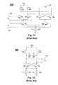
- FIG. 1Aillustrates a prior art frequency divider 100 used to create an oscillating signal.
- Frequency divider 100includes series connected D-flip flops 101 and 102 .
- a clock input 103provides an input to frequency divider 100 .
- Frequency divider 100utilizes input 103 to produce V out at one-half the frequency of input 103 .
- FIG. 1Billustrates an input waveform 104 and an output waveform 105 corresponding to the prior art frequency divider 100 of FIG. 1A .
- Input waveform 104corresponds to the input clock 103 of FIG. 1A .
- Output waveform 105corresponds to V out of FIG. 1A .
- Period T 2is twice as long as T 1 , and therefore, the frequency of output waveform 105 is one-half the frequency of input waveform 104 .
- FIG. 1Cillustrates example circuit 120 using source coupled logic (SCL) to implement a D-flip flop in a frequency divider.
- Frequency divider 120is useful in some applications, but has some major disadvantages.
- frequency divider 120has a high power consumption, has a limited output swing, does not drive capacitive loads well, and may have an asymmetric output waveform.
- the high power consumptioncreates a problem with battery life in mobile wireless solutions.
- the limited output swingmay limit the implementation in low voltage technologies.
- the circuitmay require additional buffering to improve capacitive drive capability.
- the asymmetric output waveformmay introduce unwanted additional frequencies which may interfere with the transmitter and receive channels of the system.
- FIG. 1Dillustrates a prior art injection-locking frequency divider 140 .
- An injection current 147is a current signal having a frequency component which is used to create V out 149 .
- the output frequency of V out 149may be one-half the frequency of I inj 147 .
- the injection current in frequency divider 140may be highly sensitive to interference from other signals on the same integrated circuit.
- power amplifiers (PAs)from other portions of an integrated chip may contribute signals into the ground plane of the integrated circuit. These signals may interfere with 147 and cause the circuit to lock to the wrong frequency.
- frequency divider 140may also be susceptible to common mode problems. In particular, frequency divider 140 may develop a common mode output at the same frequency as the injection signal.
- Embodiments of the present disclosurerelate to a scalable single-chip N ⁇ N dual-band MIMO RF transceiver module.
- the transceiverincludes a frequency synthesizer for generating a local oscillator signal used to modulate baseband signals that are to be transmitted by the transceiver and demodulate RF signals received by the transceiver.
- the transceiverfurther includes a plurality of transceiver hocks. Each transceiver block is adapted to independently transmit and receive wireless signals.
- the transceiver blocksare arranged in a line or row adjacent the frequency synthesizer.
- a first transceiver block immediately adjacent the frequency synthesizerreceives the local oscillator signal directly from the frequency synthesizer.
- the first transceiver blockuses the local oscillator signal to modulate and demodulate signals that are transmitted and received by the first transceiver block.
- the first transceiver blockincludes a local oscillator signal repeater.
- the local oscillator signal repeaterreceives the local oscillator signal, amplifies it and provides it to the next adjacent transceiver block. This process is repeated until the local oscillator signal has been distributed to each transceiver block in the MIMO RF transceiver.
- an embodiment of a modular MIMO RF transceivercomprises a frequency synthesizer generating a local oscillator signal, and a plurality of transceiver blocks.
- One or more of the transceiver blocksincludes a local oscillator signal repeater.
- the plurality of transceiver blocksare arranged sequentially from the frequency synthesizer.
- a local oscillator signal repeater associated with a first transceiver block nearest the frequency synthesizerreceives the local oscillator signal from the frequency synthesizer, amplifies the local oscillator signal and outputs the repeated local oscillator signal to a next transceiver block.
- the modular MIMO RF transceivermay comprise, for example, 3 ⁇ 3 MIMO RF transceiver.
- the transceiverincludes a local oscillator signal repeater that receives a local oscillator signal, amplifies the local oscillator signal and outputs the local oscillator signal.
- a transmitter within the transceivertransmits a received baseband signal at an RF frequency derived from the local oscillator signal.
- a receiver within the transceiverreceives an RF signal and down converts the signal to a baseband signal by mixing the received signal with the local oscillator signal.
- the transceiver modulemay be adapted to operate in dual frequency bands, based on first and second local oscillator signals.
- the dual band transceiverincludes a frequency synthesizer that generates first and second local oscillator signals.
- a first transceiver block adjacent the frequency synthesizerreceives the first and second local oscillator signals.
- the first transceiver blockis adapted to transmit a first Tx signal in a first frequency band corresponding to the first local oscillator signal and a second Tx signal in a second frequency band corresponding to the second local oscillator signal.
- the first transceiver blockis further adapted to receive a first Rx signal in the first frequency band and a second Rx signal in the second frequency band.
- the first transceiver blockincludes a first signal repeater and a second signal repeater.
- the first signal repeateris adapted to receive the first local oscillator signal from the frequency synthesizer and output the first local oscillator signal to a second adjacent transceiver block.
- the second signal repeateris adapted to receive the second local oscillator signal from the frequency synthesizer and output the second local oscillator signal to the adjacent transceiver block.
- the second transceiver blockreceives the first and second local oscillator signals from the first transceiver block.
- the second transceiver blockis adapted to transmit a third transmit signal in the first frequency band and a fourth transmit signal in the second frequency band.
- the second transceiver blockis further adapted to receive a third received signal in the first frequency band and a fourth received signal in the second frequency band.
- Still another embodimentprovides a scalable MIMO transceiver system.
- the scalable MIMO transceiver systemincludes a frequency synthesizer generating a local oscillator signal and a plurality of transceiver blocks arranged in a row adjacent the frequency synthesizer.
- a plurality of local oscillator signal repeatersare associated with the plurality of transceiver blocks.
- the local oscillator signalis provided to a first transceiver block in the plurality of transceiver blocks for modulating baseband signals to be transmitted by the first transceiver block with a carrier signal having a frequency based on the local oscillator signal, and demodulating signals received by the first transceiver block in a frequency band determined by the local oscillator signal.
- a first local oscillator signal repeater associated with the first transceiver blockreceives the local oscillator signal from the frequency synthesizer and forwards the local oscillator signal to a second transceiver block in the plurality of transceiver blocks.
- the second transceiver blocksimilarly modulates baseband signals to be transmitted by the second transceiver block with a carrier signal having a frequency based on the local oscillator signal, and demodulates signals received by the second transceiver block in a frequency band determined by the local oscillator signal.
- the present inventionincludes a method for use in a MIMO. Accordingly, a method of providing a modular MIMO transceiver is disclosed. The method includes providing a frequency synthesizer for generating a local oscillator signal and providing a plurality of transceiver blocks that include local oscillator signal repeaters. The method next calls for sequentially arranging the plurality of transceiver blocks in a row adjacent the frequency synthesizer. When the transceiver blocks are so arranged, the method calls for providing the local oscillator signal from the frequency synthesizer to a first transceiver block immediately adjacent the frequency synthesizer and repeating the local oscillator signal using the local oscillator signal repeater included with the first transceiver block. The method then calls for providing the repeated local oscillator signal to a second transceiver block immediately adjacent the first transceiver block.
- embodiments of the present inventionmay be used to generate oscillating signals.
- One embodiment of the present inventionincludes a circuit that receives a differential signal to be divided. The circuit converts the differential signal into an injection signal. The injection signal is coupled to an oscillator, and the oscillator generates an output signal having a frequency that is a fraction of the frequency of the differential input signal.
- the present inventionincludes a MIMO wireless communication system. The MIMO system may use the divider circuit to divide a local oscillator signal with reduced common mode distortion.
- the present inventionis a circuit including an oscillator, a load, and a differential injection circuit.
- the differential injection circuitshave a differential input coupled to receive a differential input signal having a first frequency, a first output coupled to the load, and a second output coupled to the oscillator to provide a first injection signal to the oscillator.
- the oscillatorprovides a differential output signal having a second frequency which is a fraction of the first frequency of the differential input signal.
- the second frequency of the differential output signalis one-half the first frequency of the differential input signal.
- the oscillatorlocks to a fractional frequency of the first injection signal.
- the circuitmay include an impedance coupled between the oscillator and a reference voltage for reducing common-mode signal components at the output of the oscillator.
- the impedanceis a resistor, such as an integrated resistor.
- the impedanceis a transistor, which may be biased to provide impedance.
- the differential injection circuitcomprises a first transistor and a second transistor.
- a control terminal of the first transistoris coupled to receive a first component of the differential input signal and a control terminal of the second transistor is coupled to receive a second component of the differential input signal.
- a first terminal of the first transistoris coupled to a first terminal of the second transistor (e.g., common sources). Additionally, a second terminal of the first transistor is coupled to the load and a second terminal of the second transistor is coupled to the oscillator.
- the oscillatorcomprises cross-coupled transistors each having a source coupled to an output of the differential injection circuit to receive the first injection signal and a resonant circuit coupled to the cross-coupled circuit.
- the present inventionincludes a method comprising receiving a differential input signal to be divided, the differential input signal having a first frequency, converting the differential input signal into an injection current having the first frequency, coupling the injection current to an input of an oscillator, and generating a differential output signal in the oscillator having a second frequency based on the injection current, wherein the second frequency is a fraction of the first frequency of the differential input signal to be divided.
- the second frequency of the differential output signalis one-half the first frequency of the differential input signal.
- the oscillatorlocks to a fractional frequency of the injection current.
- the methodfurther comprises coupling a current from a reference voltage to the oscillator through an impedance to dampen common mode frequency components and not dampen differential frequency components of the differential output signal.
- the present inventionincludes a wireless communication system comprising a frequency synthesizer for generating a local oscillator signal, one or more wireless transceivers.
- Each transceivercomprises a wireless receiver comprising a down-converter, the down-converter receiving a first RF signal modulated at a first frequency and the local oscillator signal, and in accordance therewith, produces a demodulated baseband signal.
- Each transceiveralso comprises a wireless transmitter comprising an up-converter, the up-converter receiving a baseband signal and the local oscillator signal, and in accordance therewith, produces a second RF signal modulated at the first frequency.
- the frequency synthesizergenerates a local oscillator signal having a second frequency for transmission across an integrated circuit, and the local oscillator signal is divided by a fractional value in each transceiver to said first frequency for use in down-converting RF signals and up-converting baseband signals.
- the wireless communication systemmay be implemented on an integrated circuit for example.
- the one or more transceiverscomprise a plurality of transceivers, and each transceiver is operable in a first and second mode.
- the frequency synthesizergenerates first and second local oscillator signals having different frequencies. In the first mode, at least one transceiver transmits and receives RF signals using the first local oscillator signal, and in the second mode the at least one transceiver transmits and receives RF signals using the second local oscillator signal.
- the frequency synthesizercomprises an oscillator, a load, and a differential injection circuit as set forth above having a differential input coupled to receive a differential input signal having a first frequency, a first output coupled to the load, and a second output coupled to the oscillator to provide a first injection signal to the oscillator.
- the oscillatorprovides a differential output signal having a second frequency which is a fraction of the first frequency of the differential input signal.
- the present inventionincludes a circuit comprising means for receiving a differential input signal and generating a differential output signal, the differential output including an injection signal, such as a current.
- the circuitfurther includes means for generating an differential output signal in response to the injection signal, the differential output signal having a frequency that is a fraction of the frequency of the differential input signal.
- the circuitmay further include means for loading a second output signal of the differential output signals.
- the circuitincludes means for generating a resonant oscillating signal in response to the injection current.
- the circuitincludes means for damping common mode frequency components in the output signal.
- the means for dampingalso provides power to the oscillator.
- the means for dampingprovides an impedance between the oscillator and a reference voltage.
- FIG. 1Aillustrates a prior art frequency divider used to create a serial clock signal.
- FIG. 1Billustrates an input waveform and an output waveform corresponding to the prior art frequency divider of FIG. 1A
- FIG. 1Cillustrates a prior art frequency divider circuit.
- FIG. 1Dillustrates another prior art frequency divider circuit.
- FIG. 2is a block diagram of a modular 3 ⁇ 3 MIMO RF transceiver.
- FIG. 3is a block diagram of a transceiver block for use in a modular transceiver such as that shown in FIG. 2 .
- FIG. 4is a circuit diagram showing circuitry for providing a local oscillator signal and a local oscillator signal repeater.
- FIG. 5is a circuit diagram of a double balanced Gilbert Cell signal mixer.
- FIG. 6is a block diagram of a 3 ⁇ 3 MIMO RF transceiver and corresponding WLAN baseband circuitry in which both Tx and Rx signals share common sets of signal interface pins.
- FIG. 7illustrates a frequency synthesizer according to one embodiment of the present invention.
- FIG. 8Aillustrates a frequency divider according to one embodiment of the present invention.
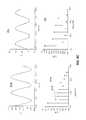
- FIGS. 8B-Care plots of the time-domain and frequency-domain performance of frequency dividers.
- FIG. 9illustrates a frequency divider according to one embodiment of the present invention.
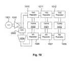
- FIG. 10illustrates a MIMO system with a distributed LO according to one embodiment of the present invention.
- the present disclosurerelates to a scalable N ⁇ N single-chip dual-band MIMO RF transceiver module compatible with the IEEE 802.11n standard for WLAN applications.
- a modular design approachallows a transceiver of substantially any dimension to be created on a single chip that may be easily integrated with other system components.
- An embodiment of such a transceiver described hereincomprises a 3 ⁇ 3 MIMO RF transceiver supporting three spatial streams and capable of delivering PHY rates up to 450 Mb/s.
- the 3 ⁇ 3 MIMO transceiver moduleincludes three substantially identical transceiver blocks and a common local oscillator. Each transceiver block includes transmitters and receivers for transmitting and receiving signals in two distinct frequency bands.
- the transceiver blocksfurther include local oscillator signal repeaters for receiving the local oscillator signals and forwarding them to subsequent transceiver blocks.
- FIG. 2is a block diagram of a modular 3 ⁇ 3 MIMO RF transceiver 200 .
- the 3 ⁇ 3 MIMO RF transceiver 200comprises a local oscillator 202 and three substantially identical transceiver blocks 204 , 206 , 208 .
- the frequency synthesizer 202 and the three transceiver blocks 204 , 206 , 208are arranged on a single integrated circuit chip in the manner shown, with the local oscillator 202 located along a bottom edge of the chip and the transceiver blocks 204 , 206 , 208 , cascaded in ascending order above the local oscillator 202 .
- the modular MIMO transceiver module 200is scalable in that a transceiver module of substantially any size may be provided by producing integrated circuit chips having more or fewer identical transceiver blocks arranged in a similar manner.
- the transceiver 200is a dual band transceiver.
- Each transceiver block 204 , 206 , 208is adapted to transmit and receive RF signals in two distinct frequency bands.
- the transceivers 204 , 206 , 208are adapted to transmit and receive RF signals in a first frequency band from 4.915 GHz to 5.825 GHz and a second frequency band from 2.412 GHz to 2.484 GHz.
- these two frequency bandswill simply be referred to as a 5 GHz band and a 2.5 GHz band.
- the local oscillator 202For optimal performance the local oscillator 202 generates a pair of phase-synchronized local oscillator signals 212 , 214 that are provided to the transceiver blocks 204 , 206 , 208 for modulating and demodulating the transmit (Tx) and receive (Rx) signals.
- the local oscillator signals 212 , 214are distributed to the transceiver modules at approximately twice the corresponding channel frequency. Accordingly, the local oscillator 202 generates local oscillator signals 212 , 214 of approximately 5 GHz and 10 GHz.
- the local oscillator 202comprises a frequency synthesizer 203 that generates a 10 GHz local oscillator signal 212 .
- the 10 GHz signalis actually in the frequency range from approximately 9.6 GHz-11.64 GHz.
- the first local oscillator signal 212is referred to as the 10 GHz signal, though one will realize that this is a nominal value which may fall anywhere in the 9.6 GHz-11.6 GHz frequency band.
- the frequency synthesizer 203employs a pair of voltage controlled oscillators (VCOs). These are followed by a dual-input single-output VCO buffer to generate the 10 GHz local oscillator signal 212 .
- VCOsvoltage controlled oscillators
- the local oscillator 202includes a divide-by-two frequency divider 205 which divides the frequency of the 10 GHz local oscillator signal 212 approximately in half to obtain the second 5 GHz local oscillator signal 214 .
- the frequency of this second local oscillator signalwill fall within a range of frequencies, in this case, 4.8 GHz-5.8 GHz, however, for convenience it is simple referred to as a 5 GHz local oscillator signal.
- the most straightforward technique for frequency divisionemploys source coupled logic (SCL) dividers. Due to large capacitive loading, however, this solution is not well suited for the present application.
- SCLsource coupled logic
- a divide by 2 ILFD 210divides the 10 GHz local oscillator signal 212 to generate the 5 GHz local oscillator signal 214 .
- Providing two local oscillator signals 212 , 214increases the potential frequency range of the MIMO transceiver. Typically only one local oscillator signal will be active at a time, depending on the operating mode of the MIMO transceiver.
- the first and second local oscillator signals 212 , 214are input to the first transceiver block 204 .
- the first transceiver block 204uses the local oscillator signals 212 , 214 to modulate signals that are to be transmitted by the first transceiver block 204 and to demodulate signals that are received by the first transceiver block 204 .
- the first transceiver block 204includes first and second local oscillator signal repeaters 216 , 218 .
- the first and second local oscillator signal repeaters 216 , 218receive the first and second local oscillator signals 212 , 214 from the frequency synthesizer and amplify them prior to forwarding them on to the second transceiver block 206 .
- Current-mode local oscillator repeatersmay be employed in each transceiver block 204 , 206 , 208 to achieve the maximum possible bandwidth.
- the local oscillator signal received from the frequency synthesizer 202 or from the previous transceiver blockis passed through a common-gate amplifier to convert the signal back to voltage mode locally, where the current mode signal is amplified and passed on to the next transceiver block.
- the repeater amplitudeis calibrated to ensure the same performance for each transceiver.
- the second transceiver block 206also uses the first and second local oscillator signals 212 , 214 to modulate and demodulate signals that are to be transmitted by and which are received by the second transceiver block 206 .
- the second transceiver block 206similarly includes first and second local oscillator signal repeaters 220 , 222 .
- the first and second local oscillator signal repeaters 220 , 222receive the first and second local oscillator signals 212 , 214 from the first transceiver block 204 , amplify them, and forward them to the third transceiver block 208 .
- the third transceiver block 208uses the first and second local oscillator signals 212 , 214 to modulate and demodulate signals that are to be transmitted by and which are received by the third transceiver block 208 .
- the third transceiver block 208may or may not include first and second local oscillator signal repeaters 224 , 226 .
- the transceiver 200comprises a 3 ⁇ 3 MIMO RF transceiver
- there is no need for the local oscillator signal repeaters in the third transceiver block 208since the first and second local oscillator signals need not be forwarded to a fourth transceiver block.
- the third transceiver block 208may include first and second local oscillator signal repeaters 224 , 226 as shown in FIG. 2 , even when they may not actually used.
- the 3 ⁇ 3 MIMO transceiver 200 of FIG. 2could be readily expanded to a 4 ⁇ 4 MIMO RF transceiver by simply adding an additional transceiver block to the chip without modifying the third transceiver block in any way.
- the layout of the MIMO RE transceiver 200has a number of advantages.
- the linear arrangement of the transceiver modules 204 , 206 , 208provides significant physical separation between the Tx Ports of each transceiver block so that separate Tx signals of the same frequency but output by the different transceiver blocks do not interfere with one another.
- the linear arrangement of the transceiver modulesalso improves the path matching characteristics of the MIMO RF transceiver 200 .
- the modular design approachis easily scalable in that MIMO RF transceivers of different sizes may be developed and manufactured without significant redesign requirements.
- the transceiver block 300may be one of the transceiver blocks 204 , 206 , 208 in the 3 ⁇ 3 MIMO transceiver 200 of FIG. 2 , or the transceiver may be part of some other sized or differently arranged transceiver.
- the transceiver block 300includes first and second transmitter portions 394 , 400 , and first and second receiver portions 396 , 398 . Both the transmitter portions 394 , 400 and the receiver portions 396 , 398 employ a direct-conversion architecture with local oscillator signals operating at twice the carrier frequency.
- the transceiver blockis operable at multiple frequencies.
- the blockincludes two repeaters for receiving two different frequency local oscillator (“LO”) signals for up-converting and down-converting signals received by and transmitted from the system.
- a first repeater 326receives a 12 GHz signal and a second repeater 328 receives a 5 GHz signal.
- Repeater 326receives the 12 GHz signal and outputs the signal on a first signal line LO_OUT 2 to be use by other circuitry such as another transceiver.
- Repeater 326also includes an output coupled through divider 332 to up-coverters 338 and 340 and down-converters 370 and 372 .
- the divided version of the LO signalis used for modulating signals to be transmitted and demodulating received signals.
- repeater 328receives the 5 GHz signal and outputs the signal on a first signal line LO_OUT 1 to be use by other circuitry such as another transceiver.
- Repeater 328also includes an output coupled through divider 330 to up-coverters 366 and 368 and down-converters 334 and 336 . Accordingly, the two divided LO signals at different frequencies are used to send and receive information across two different wireless channels at two different frequencies.
- the first local oscillator signal repeater 326receives a first local oscillator signal input 386 and provides a first local oscillator signal output 390 .
- the second local oscillator signal repeater 328receives a second local oscillator signal 388 and provides a second local oscillator signal output 392 .
- the transceiver 300includes a first divide-by-two frequency divider 330 , and a second divide-by-two frequency divider 332 .
- the transceiver architecturerequires the divide-by-two circuits for generating appropriate carrier signals for up-converting baseband transmit signals to the RF operating frequency bands of the dual band transceiver, and down-converting received RF signals to baseband.
- the divide-by-two circuitsmay comprise modified versions of a conventional CML static frequency divider in order to achieve higher operating frequencies.
- One example of a modified CML divider that may be used in some applicationsis described below.
- the first divide-by-two frequency divider 330divides the frequency of the first local oscillator signal 386 in half to provide a first carrier signal having a frequency equal to one-half the first local oscillator signal frequency.
- the second divide-by-two frequency divider 332divides the frequency of the second local oscillator signal 388 in half to provide a second carrier signal having a frequency equal to one-half the second local oscillator signal frequency.
- the frequency of the first local oscillator signalis approximately 10 GHz and the frequency of the second local oscillator signal is approximately 5 GHz. Therefore, in the embodiment shown in FIG. 3 , the frequency of the first carrier signal output from the first divide-by-two frequency divider will be approximately 5 GHz and the frequency of the second carrier signal output from the second divide-by-two frequency divider will be approximately 2.5 GHz.
- the transceiver module 300receives baseband I/Q signals Tx_I 302 and Tx_Q 304 .
- the signal path for the Tx_I signal 302includes a third order low-pass filter 310 and a variable gain amplifier 318 .
- the signal path for the Tx_Q signal 304similarly includes a third order low-pass filter 312 and a variable gain amplifier 320 .
- the first transmitter portion 394 of the transceiver block 300includes a first signal mixer 334 and a second signal mixer 336 .
- the first signal mixer 334up-converts the Tx_I baseband signal 302
- the second mixer 336up-converts the Tx_Q baseband signal 304 to the frequency band corresponding to the first carrier signal output from the first divide-by-two frequency divider 320 .
- a summing junction 342combines the output from the two mixers 334 , 336 and provides the combined signal to a variable gain amplifier (VGA) 344 and a pre-power amplifier (PPA) 346 .
- VGAvariable gain amplifier
- PPApre-power amplifier
- the output of the pre-power amplifier 346comprises a 2.5 GHz transmit signal Tx 2 _O 348 .
- the second transmitter portion 400 of the transceiver block 300includes a third signal mixer 338 and a fourth signal mixer 340 .
- the third signal mixer 338up-converts the Tx_I baseband signal 302 and the fourth mixer 340 up-converts the Tx_Q baseband signal 304 to the frequency band corresponding to the second carrier signal output from the second divide-by-two frequency divider 332 .
- a summing junction 350combines the output of the two mixers 338 , 334 and provides the combined signal to a variable gain amplifier (VGA) 352 and a pre-power amplifier (PPA) 354 .
- VGAvariable gain amplifier
- PPApre-power amplifier
- the output of the pre-power amplifier 354comprises a 5 GHz transmit signal Tx 5 _O 356 .
- the RF VGAs 344 , 352 and PPAs 344 , 354amplify the signals and provide coarse gain adjustments.
- the transmittershave a gain range of 36 dB in steps of 0.5 dB.
- the derivative superposition (DS) methodmay be implemented in the RF amplifier stages.
- the DS methoduses two parallel FETs of different widths and gate biases (one biased at class-C mode, the other at class-A mode) to achieve a composite de transfer characteristic with an extended input range in which the 3rd-order derivative of the combined current is close to zero.
- the PPA output stage 346is still designed as a traditional class-AB amplifier.
- the first and second receiver portions 396 , 398 of the transceiver block 300comprise direct conversion receivers.
- the first receiver portion 396receives a first receive signal Rx 2 _IN 358 .
- Rx 2 _INhas a frequency in the 2.5 GHZ frequency band.
- the first received signal Rx 2 _IN 358is input to a first low-noise amplifier (LNA) 362 .
- LNAlow-noise amplifier
- Differential LNAsare typically used in many receiver designs, especially in the direct-conversion architecture, to minimize various undesirable effects such as DC offsets.
- Single-ended LNAsmay be chosen to reduce power consumption, reduce the form factor of the transceiver integrated circuit, and reduce the number of RF ports required for each transceiver.
- Single-ended LNA architectureconsists of an inductively degenerated common source stage. The supply voltage of the LNA is heavily regulated to reduce supply noise coupling to the LNA stage 362 .
- the first received signalis split and provided to fifth and sixth I/Q signal mixers 366 , 368 .
- the fifth and sixth I/Q mixers 366 , 368down-convert the received RF signal to the desired baseband, in order to extract the I/Q baseband components of the first receive signal Rx 2 _IN 358 .
- the down-conversion mixermay comprise a double balanced Gilbert Cell based mixer 500 as shown in FIG. 5 .
- the PMOS device 502is used as a current-reuse transconductor.
- the same transistor 502is also used to achieve a balance between low flicker noise and third order input intercept preferred setpoint (IIP3) performance in the switching core.
- Common mode degeneration resistors 504are utilized for both the NMOS and PMOS gain matching branches to improve second order input intercept preferred setpoint (IIP 2 ) and I/Q gain matching.
- the second receiver portion 398 of the transceiver block 300is substantially similar to the first receiver portion 396 .
- the second receiver portion 398receives a second signal Rx 5 _IN 360 .
- Rx 5 _IN 360has a frequency in the 5 GHZ band.
- the second received signal Rx 5 _IN 360is input to a second low-noise amplifier (LNA) 364 .
- the second receive signal Rx 5 _INis then split and provided to seventh and eighth signal mixers 370 , 372 .
- the seventh and eight mixers 370 , 372down-convert the received RF signal to the baseband frequency in order to extract the I/Q baseband components of the second receive signal Rx 5 _IN 360 .
- the down-conversion mixers 370 , 372may each comprise double balanced Gilbert Cell based mixers 500 as shown in FIG. 5 .
- the output of the fifth signal mixer 366(the Rx_I component of the first received signal) is connected to the output of the seventh signal mixer 370 at circuit node 382 .
- the output from either the fifth signal mixer 366 or the seventh signal mixer 370is then input to a first transimpedance amplifier 378 .
- the output of the sixth signal mixer 368(the Rx_Q component of the first received signal) is connected to the output of the eighth signal mixer 372 at a circuit node 384 .
- the output from either the sixth signal mixer 368 or the eighth signal mixer 372is input to a second transimpedance amplifier 380 .
- the transimpedance amplifiersimprove mixer linearity by reducing the signal swing at the drain of the mixers' switching cores.
- the Rx_I signalis filtered by a low-pass filter 322 , amplified by a baseband variable gain amplifier 314 , and output as the received signal Rx_ 1306 .
- the Rx_Q signalis filtered by a low-pass filter 324 , amplified by a baseband variable gain amplifier 316 and output as the received signal Rx_Q 308 .
- the low pass filters 322 , 324reject blocking signals, and the baseband VGAs 314 , 316 fine-tune the gain to the optimal level before digitization.
- the received error vector magnitude signal(EVM) strongly depends on the signal-to-noise ratio (SNR) and the distortion of the receiver.
- SNRsignal-to-noise ratio
- Signal detectorsmay be located at various positions in the receiver chain to ensure that the various components are operating within their linearity limits.
- the gain switching point of the LNAs and LPFsis optimized so that EVM is minimized for a wide input power range.
- the local oscillator signal repeaters in the transceiver blocks 204 , 206 , 208 of FIG. 2may comprise current mode repeaters to maximize potential bandwidth.
- FIG. 4shows a modular MIMO transceiver 400 that includes a local oscillator 402 and a transceiver block 404 .
- the modular transceiver 400may include any number of additional transceiver blocks 404 , but for purposes of illustrating a current mode local oscillator signal reater just one transceiver block is shown, with the understanding that the current mode local oscillator signal repeaters in other transceiver blocks will be substantially identical to that shown in the transceiver block 404 in FIG. 4 .
- the local oscillator 402includes a frequency synthesizer 403 that generates the first 10 GHz local oscillator signal 412 .
- the local oscillator 402further includes a divide by 2 frequency divider 405 for generating the second, 5 GHz, local oscillator signal 414 .
- a voltage-to-current mode transconductance stage 408is shown for converting the 10 GHz local oscillator signal from a voltage signal to a current signal. Although not shown in FIG. 4 , a similar transconductance stage is provided for the 5 GHz signal 414 output from the divide by 2 frequency divider 405 .
- the voltage-to-current mode transconductance stage 408comprises a pair of MOSFET transistors 410 and a current source 412 .
- the drains of the two MOSFET devices 410are connected in a common drain arrangement with the drains of both MOSFET devices connected to the input of the current source 412 .
- the 10 GHz voltage signal output from the frequency synthesizeris applied to the gates of the two MOSFET devices, the source terminals of the two MOSFET devices 410 provide the 10 GHz current mode local oscillator signal 414 that is provided to the first transceiver block 404 .
- the 10 GHz local oscillator signal repeater 418 in the first transceiver block 404includes a common gate amplifier circuit 420 , a voltage-to-current mode transconductance stage 422 .
- the common gate amplifier 420comprises a pair of MOSFET transistors 424 connected in a common gate arrangement, and a tuned LC loading circuit 426 , connected to the source terminals of the two MOSFET devices 424 .
- the 10 GHz current mode local oscillator signal 414is connected to the drains of the two MOSFET, devices 424 .
- the two MOSFET devices 424 and the LC loading circuit 426convert the 10 GHz current mode local oscillator signal back into a voltage signal.
- the converted voltage signalis then provided to a frequency divider 427 , and is used for upconverting and downconverting signals transmitted and received by the transceiver blocks in FIG. 2 , for example.
- the converted voltage signalis also provided to the voltage-to-current transconductance stage 422 in the same manner that the 10 GHz local oscillator signal generated by the frequency synthesizer 403 was provided to the voltage-to-current transconductance stage 408 of the local oscillator 402 .
- the voltage-to-current transconductance stage 422 of the local oscillator signal repeater 418is substantially identical to the voltage-to-current mode transconductance stage 408 of the local oscillator 408 , including a pair of MOSFET transistors 428 connected in a common drain arrangement with a current source 430 .
- the source terminals of the two MOSFET devices 428provide the 10 GHz current mode local oscillator signal 412 to the next transceiver block in the modular MIMO transceiver.
- the MIMO RF transceiver 200 of FIG. 2may be capable of transmit and receive I/Q calibration.
- a baseband single tonemay be applied to an input of the transmitter.
- the resulting RF spectrum of the up-converted tonesconsists of the main RF tone and the sideband tone from I/Q mismatch.
- This signalis loop-backed to the receiver and down-converted to baseband using a low IF receiver.
- the received signalmay then be analyzed for I/Q compensation in the digital domain.
- the transceiver layoutmay also be employed to reduce the number of pins required for interfacing the RF transceiver integrated circuit chip with the baseband circuitry of a WLAN-system.
- a typical RF transceiver blocksuch as transceiver blocks 204 , 206 , 208 in FIG. 2 requires a total of four pins for receiving a baseband I/Q transmit signal from the WLAN baseband circuitry. These include Tx_I+ and Tx_I ⁇ pins for receiving the Tx_I component of the transmit signal, and Tx_Q+ and Tx_Q ⁇ pins for receiving the Tx_Q component of the transmit signal.
- a typical RF transceiver blockrequires four pins for interfacing baseband I/Q signals received by the receiver portion of the transceiver with the baseband circuitry of the WLAN system. These include Rx_I+ and Rx_I ⁇ pins for interfacing the Rx_I component of the received signal to the baseband circuitry, and Rx_Q+ and Rx_Q ⁇ pins for providing the Rx_Q component of the received signal to the baseband circuitry. Thus, 8 pins total are required for interfacing signals between a single RF transceiver block and the baseband portion of the WLAN circuitry. In the 3 ⁇ 3 transceiver module 200 of FIG. 2 this adds up to a total of 24 pins for interfacing Tx and Rx signals between the transceiver module 200 and the baseband circuitry.
- the transceiver blocks 204 , 206 , 208cannot transmit and receive signals simultaneously. Therefore, the number of interface pins could be reduced by half by sharing the same set of pins for interfacing both Tx and Rx signals.
- a multiplexer or other switching mechanism associated with the transceivermay be employed to connect the interface pins to the transmitter portion of the transceiver during a transmitting mode of operation, and to the receiver portion of the transceiver during a receiving mode.
- baseband signals from the WLAN circuitrymay be applied to the four interface pins associated with the transceiver block as described and transmitted by the transmitting portion of the transceiver.
- the multiplexer or other switching mechanismmay connect down-converted baseband signals received by the receiver portion of the transceiver block to the same set of interface pins to convey the received signals from the transceiver block to the WLAN baseband circuitry.
- the total number of interface pins in a 3 ⁇ 3 transceiver modulemay be reduced from 24 to 12.
- a transceiver blockIn order to perform an I/Q calibration loop back test, however, a transceiver block must be able to receive Tx signals from the baseband circuitry, and provide Rx signals to the baseband circuitry simultaneously. In conducting such a test, a single tone signal is generated in the baseband circuitry and is applied to the input of the transmitter. The transmitter up-converts the signal to RF frequency and loopback circuitry couples the transmitted signal back to the receiver. The transceiver down converts the received test signal and provides the baseband signal to the WLAN baseband circuitry, which analyzes the received test signal to determine the amount of I/Q compensation required for satisfactory operation of the communication channel.
- FIG. 6A 3 ⁇ 3 modular MIMO RF transceiver 600 similar to the transceiver module 200 shown in FIG. 2 is provided.
- the transceiver module 600includes a frequency synthesizer 602 and three substantially similar transceiver blocks: Transceiver block A 604 , Transceiver block B 606 , and Transceiver block C 608 .
- the frequency synthesizerprovides a pair of local oscillator signals 652 , 654 to the transceiver blocks 604 , 606 , 608 for modulating and demodulating signals transmitted and received by the transceiver blocks 604 , 606 , 608 .
- the transceiver blocks 604 , 606 , 608comprise dual band transceivers capable of transmitting and receiving signals in two distinct frequency bands.
- Transceiver block A 604transmits a first set of 5 GHz and 2.5 GHz Tx signals 628 , 630 and receives a first set of 5 GHz and 2.5 GHz Rx signals 632 , 634 .
- Transceiver block B 606transmits a second set of 5 GHz and 2.5 GHz Tx signals 636 , 638 and receives a second set of 5 GHz and 2.5 GHz Rx signals 640 , 642 .
- Transceiver block Ctransmits a third set of 5 GHz and 2.5 GHz Tx signals 644 , 646 , and receives a third set of 5 GHz and 2.5 GHz Rx signals 648 , 650 .
- transceiver block A 604includes TBB block 610 and RBB block 612 .
- Transceiver block B 606includes TBB block 614 and RBB block 616 .
- Transceiver block C 608includes TBB block 618 and RBB block 620 .
- the 3 ⁇ 3 MIMO RF transceiver module 600further includes three multiplexers 622 , 624 , 626 .
- the multiplexers 622 , 624 , 626switch between transmit and receive modes of operation.
- the multiplexers 622 , 624 , 626connect Tx signals received from the WLAN baseband circuitry 660 to the TBB blocks 612 , 614 , 618 associated with the various transceiver blocks 604 , 606 , 608 .
- the multiplexers 622 , 624 , 626connect down-converted baseband Rx signals from the RBB blocks 612 , 616 , 620 to the baseband circuitry 660 .
- An internal bus structure 656 on the MIMO RF transceiver 600 integrated circuit chiproutes signals between the various TBB blocks 610 , 614 , 618 and RBB blocks 612 , 616 , 620 and the multiplexers 622 , 624 , 626 .
- the 3 ⁇ 3 MIMO RF transceiver 600supports three separate communication sub-channels, each associated with one of the transceiver blocks 604 , 606 , 608 . These may be identified as communication sub-channels A, B and C. Each communication sub-channel supports both Tx and Rx signals. Thus, communication sub-channel A supports transmit signals Tx_A which originate in the WLAN baseband circuitry 660 and are provided to the MIMO RF transceiver 600 for transmission to one or more external devices. Communication sub-channel A further supports received signals Rx_A which are received by the MIMO RF transceiver 600 from one or more external devices and provided to the WLAN baseband circuitry 660 . Similarly, communication sub-channel B supports transmit signals Tx_B and receive signals Rx_B.
- the WLAN baseband circuitry 660includes a digital-to-analog converter DAC A 668 for converting digital signals into the analog baseband Tx_A signals for transmission over communication sub-channel A.
- the WLAN baseband circuitry 660further includes digital-to-analog converter DAC B 672 for converting digital signals into analog baseband Tx_B signals for transmission over communication sub-channel B.
- the WLAN baseband circuitry 660includes digital-to-analog converter DAC C 676 for converting digital signals into analog baseband Tx_C signals for transmission over communication sub-channel C.
- the WLAN baseband circuitry 660further includes analog-to-digital converter ADC A 674 for converting analog baseband Rx_A signals received over communication sub-channel A into digital signals, analog-to-digital converter ADC B 678 for converting analog baseband Rx_B signals received over communication sub-channel B into digital signals, and analog-to-digital converter ADC C 676 for converting analog baseband signals Rx_C received over communication sub-channel C into digital signals.
- the WLAN baseband circuitry 660further includes first, second and third multiplexers 662 , 664 , 666 .
- the multiplexers 662 , 664 , 666 associated with the WLAN baseband circuitry 660switch between transmit and receive modes of operation.
- the multiplexers 662 , 664 , 666connect Tx signals from the digital-to-analog converters 668 , 672 , 676 to the transceiver module 600 .
- the multiplexers 662 , 664 , 666connect baseband Rx signals received by the transceiver to the analog-to-digital converters 670 , 674 , 678 .
- the WLAN baseband circuitry 660interfaces with the MIMO RF transceiver 600 via three distinct signal paths 680 , 682 , 684 .
- Each signal path 680 , 682 , 684comprises four conductors (corresponding to pins on the transceiver integrated circuit chip package) connecting the WLAN baseband multiplexers 662 , 664 , 666 to the MIMO RF transceiver multiplexers 622 , 624 , 626 .
- each signal path 680 , 684 , 686is capable of carrying one of either a baseband I/Q Tx signal (Tx_I+, Tx_I ⁇ , Tx_Q+, Tx_Q ⁇ ) from the WLAN baseband circuitry 660 to the MIMO RF transceiver 600 , or a baseband I/Q Rx signal (Rx_I+, Rx_I ⁇ , Rx_Q+, Rx_Q ⁇ ) from the MIMO RF transceiver 600 to the WLAN baseband circuitry 660 . Since the transmit and receive signals share the signal paths 680 , 682 , 684 , only 12 conductors are required to interface the MIMO RF transceiver 600 with the WLAN baseband circuitry 660 .
- the problem of performing the 1/Q calibration loop-back test while sharing the interface connections between both Tx and Rx signalsis avoided by routing corresponding Tx and Rx signals from the same transceiver block 604 , 606 , 608 to separate multiplexers 622 , 624 , 626 of the MIMO RF transceiver 600 , so that an outgoing Tx test signal and the corresponding incoming Rx test signal travel across separate signal paths between the MIMO RF transceiver 600 and the WLAN baseband circuitry 660 .
- the internal bus structure 656 of the MIMO RF transceiver module 600routes outgoing Tx_A signals from the first multiplexer 622 to the TBB block 610 in transceiver block A 604 , while incoming Rx_A signals are routed from the RBB block 612 in transceiver block A 604 to the second transceiver multiplexer 624 .
- the first multiplexer 622is connected to the first communication path 680 between the WLAN baseband circuitry 660 and the transceiver module 600
- the second multiplexer 624is connected to the second signal path 682 between the WLAN baseband circuitry 660 and the transceiver module 600 .
- Tx_A signalscross the interface between the WLAN baseband circuitry 660 and the transceiver module 600 over the first signal path 680
- Rx_A signalscross the interface over the second signal path 682
- outgoing Tx_B signalsare routed from the second transceiver multiplexer 624 to the TBB block 614 in transceiver block B 604
- incoming Rx_B signalsare routed from the RBB block 616 in transceiver block B 604 to the third transceiver multiplexer 626 .
- the second transceiver multiplexer 624is connected to the second signal path 684 between the transceiver module 600 and the WLAN baseband circuitry 660 .
- the third multiplexer 626is connected to the third signal path 684 .
- Tx_B signalscross the interface between the WLAN baseband circuitry 660 and the transceiver module 600 over the second signal path 682
- Rx_B signalscross the interface over the third signal path 684 .
- outgoing Tx_C signalsare routed from the third transceiver multiplexer 626 to the TBB block 618 of transceiver C 604
- inbound Rx_C signalsare routed from the RBB block 620 of transceiver C to the first transceiver multiplexer 622 .
- Tx_C signalscross the interface between the WLAN baseband circuitry 660 and the transceiver module 600 over the third signal path 684
- Rx_C signalscross the interface over the first signal path 680 .
- the first WLAN baseband multiplexer 662is connected to the first signal path 680 between WLAN baseband circuitry and the transceiver module 600 .
- the first WLAN baseband multiplexer 662switches between connecting Tx_A signals from DAC A 668 to the first signal path 680 , and connecting Rx_B signals from the first signal path 680 to ADC C 670 .
- the second WLAN baseband multiplexer 664is connected to the second signal path 682 and switches between connecting Tx_B signals from DAC B 672 to the second signal path 682 , and connecting Rx_A signals from the second signal path 682 to ADC A 674 .
- the third WLAN baseband multiplexer 666is connected to the third signal path 684 and switches between connecting Tx_C signals from DAC C 676 to the first signal path, and connecting Rx_B signals from the third signal path 684 to ADC B 678 .
- the first transceiver multiplexer 622 and the first WLAN baseband multiplexer 662operate in the transmit mode.
- the second transceiver multiplexer 624 and the second WLAN baseband multiplexer 664operate in the receive mode.
- a test signal Tx_A testoriginates in the WLAN baseband circuitry 660 .
- the test signal Tx_A testis converted to an analog baseband signal by DAC A 668 and provided to the first WLAN baseband multiplexer 662 .
- the WLAN baseband multiplexer 662connects the Tx_A test signal to the first signal path 680 , and the first transceiver multiplexer 622 connects the first signal path 680 to TBB block 610 of transceiver block A 604 .
- the baseband signal Tx_A testis conveyed from DAC A 608 in the WLAN baseband circuitry 660 to TBB block 610 in transceiver A 604 via the first signal path 680 .
- Transceiver block A 604transmits the test signal and loopback circuitry 631 couples the transmitted test signal to the receiver portion of transceiver A 604 .
- Transceiver block A 604receives the looped back test signal as received signal Rx_A test and outputs the received test signal via the RBB block 612 .
- the Rx_A test signalis routed from the RBB block 612 to the second transceiver multiplexer 624 .
- the second transceiver multiplexer 624connects the received Rx_A test signal to the second signal path 682
- the second WLAN baseband multiplexer 664connects the second signal path 682 to ADC A 674 .
- the baseband signal Rx_A testis conveyed from the RBB block 612 in transceiver block A to ADC A 674 in the WLAN baseband circuitry 660 via the second signal path 682 .
- the ADC A 674digitizes the received Rx_A test signal, and the WLAN baseband circuitry 660 determines the level of I/Q compensation required for communication subchannel A in the digital domain. By routing the received Rx_A test signal back to the WLAN baseband circuitry 660 over a separate signal path, the conflict between the Tx_A test signal and the Rx_A test signal during the loop-back test is resolved.
- the transmit and receive signals associated with the other transceiver blocks 604 , 606are similarly routed to separate multiplexers and thus conveyed across the interface between the transceiver module 600 and the WLAN baseband circuitry 660 by separate interface signal paths.
- Tx_B signalsare routed over the second signal path 682
- Rx_B signalsare routed over the third signal path 684 .
- Tx_C signalsare routed over the third signal path 684
- Rx_C signalsare routed over the first signal path 680 .
- FIG. 7illustrates a frequency synthesizer 700 according to one embodiment of the present invention.
- Frequency synthesizer 700may be integrated into a communication system implementing a MIMO architecture as described in more detail below, for example.
- Frequency synthesizer 700includes an injection-locking frequency divider (ILFD) 701 coupled to accept a differential oscillator signal 709 from voltage controlled oscillator (VCO) 702 .
- ILFD 701includes injection circuit 704 , De-Q circuit 705 , and oscillator 703 .
- VCO 702provides a differential oscillator input signal 709 to injection circuit 704 .
- Injection circuit 704provides an injection signal 708 to oscillator 703 .
- Oscillator 703is an injection-locking oscillator which provides a differential output voltage V out 707 .
- the differential output voltage V out 707may have a frequency which is half the frequency of the differential oscillating signal 709 .
- Injection circuit 704receives a differential input signal from the VCO and generates a differential output signal, the differential output signal includes an injection signal (e.g., a current) and another signal.
- Injection signal 708has the same frequency as the differential oscillating signal 709 .
- Injection signal 708may be used to generate an injection current within oscillator 703 that is used to generate a differential output signal having a frequency that is a fraction of the differential input signal frequency as described in more detail below.
- the injection circuit 704may include a load balancing circuit 706 and a differential injection circuit 750 for generating the injection signal 708 .
- Differential injection circuit 750receives the input signal to be divided as a differential signal and couples an injection signal 708 to oscillator 703 .
- Load balancing circuit 706may include an impedance which corresponds to the impedance within oscillator 703 so that the outputs of the differential injection circuit are balanced, for example.
- differential injection circuit 704 and oscillator 703allows the frequency synthesizer 700 to be less susceptible to frequency spurs caused by power amplifiers (PAs) or by other sources.
- the frequency synthesizer 700may be integrated into a communication circuit that utilizes a plurality of PAs to transmit wireless signals. These PAs may generate spurious signals within the ground plane of the integrated circuit.
- Each complimentary signal of differential oscillating signal 709may be influenced in similar measure to the ground interference. In other words, differential signals are less susceptible to common mode distortion. Accordingly, by processing the input signal differentially to create the injection signal, the circuit may reduce susceptibility of the oscillator to common mode components, resulting in reduced common mode signals in output voltage V out 707 .
- ILFD 701may also include a de-Q circuit 705 to further reduce unwanted common mode signal components in the output signal.
- De-Q circuit 705may dampen the common mode frequency components within the injection locking oscillator in one embodiment, the de-Q circuit is an impedance coupled between the oscillator and a reference voltage such as the supply voltage.
- frequency synthesizer 700may be part of integrated circuit and oscillator 703 may include a differential resonant circuit 710 , which may include capacitors and inductors (e.g., an LC tank). The resonant circuit may include unwanted common mode frequency components from the injection signal (e.g., 1 ⁇ 2 the desired output signal).
- De-Q circuit 705may be provided to dampen the common mode frequency components, and therefore the quality factor (i.e. Q factor), while not affecting the differential components of the circuit 710 to reduce the common mode signal components at the output.
- FIG. 8Aillustrates a frequency divider 800 according to one embodiment of the present invention.
- Frequency divider 800includes differential injection circuit 850 , load balancing circuit 818 , de-Q circuit 802 , and oscillator 803 .
- Differential injection circuit 850is coupled to receive differential input signal V in 814 .
- Differential injection circuit 850receives a differential input signal to be divided and provides an injection signal (I inj ) to oscillator 803 .
- differential injection circuit 850provides an example circuit for receiving a differential input signal and generating an injection signal.
- One output of circuit 850is coupled to the oscillator 803 and the other output is coupled to load balancing circuit 818 .
- Load balancing circuitprovides a load for one output of differential circuit 850 .
- Oscillator 803receives the injection signal and locks to one-half the signal frequency.
- De-Q circuit 802is coupled to provide power to oscillator 803 and to dampen common mode frequency components as described above.
- Oscillator 803provides a differential output signal V out 815 that may have one-half the frequency of the differential input signal V in 814 .
- Differential injection circuit 850includes transistors 806 and 813 .
- the control terminal of transistor 806is coupled to receive one component of differential input signal V in 814 and the control terminal of transistor 813 is coupled to receive the other component of differential input signal V in 814 .
- load balancing circuitincludes transistors 804 and 805 . Two transistors 804 and 805 are used to match the main branch path. So 804 and 805 are miming 811 and 812 .
- the drain terminal of transistor 806is coupled to the source terminal of transistor 804 and the source terminal of transistor 805 .
- the control terminal and the drain terminal of transistor 804 and the control terminal and the drain terminal of transistor 805are coupled to reference voltage Vdd.
- the drain terminal of transistor 806produces a signal (here, a current) that is loaded by transistors 804 and 805 .
- the drain terminal of transistor 813produces the injection signal (here, also a current).
- the source terminals of transistors 806 and 813are coupled to a bias current source 816 .
- Oscillator 803includes inductor 808 , inductor 809 , capacitor 819 , capacitor 810 , and cross-coupled transistors 811 - 812 .
- One terminal of inductor 808 and 809is coupled to receive power from a reference voltage (e.g., a power supply Vdd) through resistor 802 , which is described in more detail below.
- a second terminal of inductor 808is coupled to one terminal of capacitor 819 , the drain terminal of transistor 811 and the control terminal of transistor 812 .
- a second terminal of inductor 809is coupled to one terminal of capacitor 810 , the drain terminal of transistor 812 and the control terminal of transistor 811 .
- the other terminals of capacitor 819 and 810are coupled together.
- the source terminal of transistors 811 and 812are coupled to the drain terminal of transistor 813 to receive the injection signal (i.e., current I inj ).
- the oscillator circuitgenerates a resonant oscillating signal at a frequency based on the values of the capacitors and inductors and the injection signal.
- Frequency divider 800utilizes differential to single-ended current injection to produce differential output signal V out 815 .
- Transistor 806 and 813form a differential pair.
- Differential input signal V in 814couples to the control terminal of transistor 806 and 813 and steers the current of current source 816 through transistor 806 and transistor 813 .
- Load balancing circuit 818comprised of transistors 804 and 805 , has a controlled impedance relative to the impedance as presented to the drain terminal of transistor 813 .
- the impedance of circuit 818may be matched to the impedance of the oscillator to improve the balance of current passing through transistors 806 and 813 such that each component of differential input signal V in 814 contributes proportionally to generating the injection current I inj .
- the signal provided to the control terminal of transistor 813may modulate the current I t to produce I inj .
- De-Q circuit 802is implemented using a resistor 807 .
- Resistor 807couples current from Vdd to the oscillator 803 .
- Oscillator 803may include load capacitors 816 and 817 (connected with dashed lines). These capacitances may be input parasitic capacitances of a subsequent circuit stage, for example.
- Resistor 807provides a damping effect on common mode frequency components such that a corresponding quality factor (i.e. Q factor) is reduced. Resistor 807 does not dampen the differential frequency components associated with the resonant circuit (i.e.
- inductor 808inductor 809 , capacitor 819 , and capacitor 810 ) because the node between the inductors is a virtual ground to differential signals in the LC tank. Accordingly, the quality factor associated with the differential resonant circuit remains unchanged. As a result, the common mode frequency components of the output signal are attenuated but the differential frequency components are unchange.
- FIGS. 8B and 8Cillustrate the improvement in reducing unwanted common mode frequency components.
- the input frequency for this exampleis 10.4 GHz and the output frequency is 5.2 Ghz.
- FIG. 8Bshows the waveforms at the output of a prior art injection locked oscillator.
- FIG. 8Billustrates the single ended (or common mode) time domain waveform 890 , common mode frequency domain components 891 , differential time domain waveform 892 , and the differential frequency domain components 893 .
- the common mode signalincludes a strong harmonic 895 , which is an unwanted common mode frequency component.
- FIG. 8Cshows the waveforms at the output of a injection locked oscillator of FIG. 8A , FIG.
- 8Cillustrates the single ended (or common mode) time domain waveform 890 B, common mode frequency domain components 891 B, differential time domain waveform 892 B, and the differential frequency domain components 893 B.
- the common mode harmonichas been reduced by more than 10 dB.
- FIG. 9illustrates a frequency divider 900 according to another embodiment of the present invention.
- Frequency divider 900utilizes a differential current injection circuit to produce differential output signal V out 915 .
- Divider 900includes a differential injection circuit including transistors 906 and 913 .
- Transistor 906is coupled to a load comprising transistors 904 and 905 , which are NMOS transistors having their gates and drains coupled to a supply voltage Vdd.
- Transistor 913is coupled to a load comprising an oscillator circuit.
- the differential injection circuitis biased using a resistor 903 coupled between the sources of transistors 906 and 913 and ground.
- Frequency divider 900includes biasing circuitry for setting the operating point of the differential injection circuit.
- This biasing circuitryincludes bias current source I bias 923 , transistor 920 , transistor 921 , resistor 922 , resistor 917 , resistor 919 , resistor 925 , and resistor 910 .
- I bias 923is coupled to the drain terminal and the control terminal of transistor 920 .
- the control terminal of transistor 920is also coupled to one terminal of resistor 910 and the drain terminal of transistor 921 .
- the source of transistor 920is coupled through resistor 922 to set up a bias voltage V bias on resistor 910 and across transistor 921 .
- Resistors 910 and 919couple V bias to the control terminal of transistor 906 .
- Resistors 910 and 917couple V bias to the control terminal of transistor 913 .
- the source terminal of transistor 921is coupled through resistor 925 to ground.
- the gate transistor 921is set to hold the bias value on resistor 910 .
- the differential resonant circuit 924 , transistors 904 - 906 , and transistors 911 - 913operate in a similar manner to circuit 300 of FIG. 3A described above.
- Differential input signal V in 914couples to the control terminal of transistor 906 through capacitor 918 and couples to the control terminal of transistor 913 through capacitor 916 .
- Differential input signal V in 914steers the current passing through resistor 903 from transistor 906 and transistor 913 .
- Load balancing circuit comprised of transistors 904 and 905is similar to the impedance as presented to the drain terminal of transistor 913 . This load balancing circuit may improve the balance of current passing through transistors 906 and 913 such that each component of differential input signal V in 914 contributes proportionally to generating the injection current I inj .
- Differential resonant circuit 924includes differential inductor 902 and selectable set of capacitors 907 - 909 .
- Selectable sets of capacitors 907 - 909may be chosen to change (i.e., tune) the frequency characteristics of the differential frequency divider.
- the differential inductor 902has a first terminal coupled to the first terminal of each of selectable set of capacitors 907 - 909 , the drain terminal of transistor 911 , and the control terminal of transistor 912 .
- the differential inductor 902has a second terminal coupled to the second terminal of each of selectable set of capacitors 907 - 909 , the drain terminal of transistor 912 , and the control terminal of transistor 911 .
- a center tap terminal of differential inductor 902is coupled to Vdd through the channel of transistor 901 .
- transistor 901is a PMOS transistor operating in deep triode region to act as an impedance similar to the De-Qing resistor 307 of FIG. 3 described above.
- FIG. 10illustrates a MIMO system with a distributed LO according to one embodiment of the present invention.
- Embodiments of the above described techniquemay be advantageously used in MIMO wireless integrated systems. For instance, because MIMO systems typically include several power amplifiers, it is important to overcome the common mode problems described above.
- the present inventionincludes a MIMO architecture operable at multiple frequencies, which may use a divider described above.
- the MIMO system in FIG. 10includes a voltage controlled oscillator (“VCO”) 1001 for generating a local oscillator signal.
- VCOvoltage controlled oscillator
- the local oscillator signalmay be used in the up-conversion process, the down-conversion process, or both, for example.
- the VCOmay generate a local oscillator signal having a frequency of about 10 GHz, and the MIMO transceivers are operable at 5 GHz (e.g., 802.11a) and 2.4 GHz (802.11b/g).
- the VCO signalis generated at twice the operation frequency for transmission between different locations or points on an integrated circuit. Therefore, the signal used for 802.11a (5 GHz) is propagated at 10 GHz and the signal used for 802.11b/g (2.4 GHz) is propagated at about 5 GHz.
- the 10 GHz VCO output signalis coupled to a buffer 1002 .
- the LOin 802.11a mode the LO may range between about 10 and 12 GHz, while in 802.11b/g mode the LO may range between about 4.8 and 5GHz.
- the output of buffer 1002is coupled to a plurality of 10G repeaters for receiving and passing on the signal to multiple transceivers when the transceivers are operating in 802.11a mode.
- a first output of repeater 1010is coupled to transceiver 1020 for providing an up/down conversion LO signal, and a second output is coupled to another repeater.
- the 10 GHz LO signalmay be provided to multiple transceivers (e.g., TX/RX 1021 , TX/RX 1022 , and others) in the MIMO system.
- the output of buffer 1002is also coupled to a divider 1003 .
- Divider 1003may be a divide-by-two circuit implemented using any of the techniques described above and in FIGS. 2-4 .
- the output of the divider 1003is a 5 GHz signal, which is coupled to buffer 1004 and then to repeaters 1006 - 1008 to provide up/down conversion signals to transceivers 1020 - 1022 when the transceivers are operating in 802.11b or 802.11g mode. Inside each transceiver, the LO signals are divided by one-half so they can be used to send and receive information.
Landscapes
- Engineering & Computer Science (AREA)
- Power Engineering (AREA)
- Computer Networks & Wireless Communication (AREA)
- Signal Processing (AREA)
- Transceivers (AREA)
Abstract
Description
Claims (23)
Priority Applications (2)
| Application Number | Priority Date | Filing Date | Title |
|---|---|---|---|
| US12/358,955US8577305B1 (en) | 2007-09-21 | 2009-01-23 | Circuits and methods for generating oscillating signals |
| US14/071,171US9401737B1 (en) | 2007-09-21 | 2013-11-04 | Circuits and methods for generating oscillating signals |
Applications Claiming Priority (3)
| Application Number | Priority Date | Filing Date | Title |
|---|---|---|---|
| US97429607P | 2007-09-21 | 2007-09-21 | |
| US12/235,333US8139670B1 (en) | 2007-09-21 | 2008-09-22 | Modular MIMO transceiver architecture |
| US12/358,955US8577305B1 (en) | 2007-09-21 | 2009-01-23 | Circuits and methods for generating oscillating signals |
Related Parent Applications (1)
| Application Number | Title | Priority Date | Filing Date |
|---|---|---|---|
| US12/235,333Continuation-In-PartUS8139670B1 (en) | 2007-09-21 | 2008-09-22 | Modular MIMO transceiver architecture |
Related Child Applications (1)
| Application Number | Title | Priority Date | Filing Date |
|---|---|---|---|
| US14/071,171ContinuationUS9401737B1 (en) | 2007-09-21 | 2013-11-04 | Circuits and methods for generating oscillating signals |
Publications (1)
| Publication Number | Publication Date |
|---|---|
| US8577305B1true US8577305B1 (en) | 2013-11-05 |
Family
ID=49487920
Family Applications (2)
| Application Number | Title | Priority Date | Filing Date |
|---|---|---|---|
| US12/358,955Active2030-04-03US8577305B1 (en) | 2007-09-21 | 2009-01-23 | Circuits and methods for generating oscillating signals |
| US14/071,171Expired - Fee RelatedUS9401737B1 (en) | 2007-09-21 | 2013-11-04 | Circuits and methods for generating oscillating signals |
Family Applications After (1)
| Application Number | Title | Priority Date | Filing Date |
|---|---|---|---|
| US14/071,171Expired - Fee RelatedUS9401737B1 (en) | 2007-09-21 | 2013-11-04 | Circuits and methods for generating oscillating signals |
Country Status (1)
| Country | Link |
|---|---|
| US (2) | US8577305B1 (en) |
Cited By (32)
| Publication number | Priority date | Publication date | Assignee | Title |
|---|---|---|---|---|
| US20120157011A1 (en)* | 2010-12-21 | 2012-06-21 | Stmicroelectronics S.A. | Electronic switch and communication device including such a switch |
| US20130058384A1 (en)* | 2010-03-23 | 2013-03-07 | Frequency Multiplying Transceiver | Frequency Multiplying Transceiver |
| US20130233979A1 (en)* | 2012-03-09 | 2013-09-12 | Jingwang ZHANG | Track circuit transceiver |
| US20130321198A1 (en)* | 2012-05-31 | 2013-12-05 | Electronics And Telecommunications Research Institute | Mimo radar system having multiple transmitters and receivers |
| US8649734B1 (en) | 2007-08-13 | 2014-02-11 | Marvell International Ltd. | Bluetooth scan modes |
| US8655279B2 (en) | 2008-06-16 | 2014-02-18 | Marvell World Trade Ltd. | Short-range wireless communication |
| US20140308899A1 (en)* | 2013-04-10 | 2014-10-16 | Mediatek Inc. | Multi-standards transceiver |
| US8923788B1 (en) | 2008-06-27 | 2014-12-30 | Marvell International Ltd. | Circuit and method for adjusting a digitally controlled oscillator |
| US8983557B1 (en) | 2011-06-30 | 2015-03-17 | Marvell International Ltd. | Reducing power consumption of a multi-antenna transceiver |
| US20150098541A1 (en)* | 2013-10-07 | 2015-04-09 | Assaf Ben-Bassat | Synchronizing phases between local lo generation circuits |
| US9055460B1 (en) | 2008-08-11 | 2015-06-09 | Marvell International Ltd. | Location-based detection of interference in cellular communications systems |
| US9066369B1 (en) | 2009-09-16 | 2015-06-23 | Marvell International Ltd. | Coexisting radio communication |
| US9078108B1 (en) | 2011-05-26 | 2015-07-07 | Marvell International Ltd. | Method and apparatus for off-channel invitation |
| US9125216B1 (en) | 2011-09-28 | 2015-09-01 | Marvell International Ltd. | Method and apparatus for avoiding interference among multiple radios |
| US9131520B1 (en) | 2009-04-06 | 2015-09-08 | Marvell International Ltd. | Packet exchange arbitration for coexisting radios |
| US9148200B1 (en) | 2007-12-11 | 2015-09-29 | Marvell International Ltd. | Determining power over ethernet impairment |
| US9215708B2 (en) | 2012-02-07 | 2015-12-15 | Marvell World Trade Ltd. | Method and apparatus for multi-network communication |
| US9294997B1 (en) | 2010-05-11 | 2016-03-22 | Marvell International Ltd. | Wakeup beacons for mesh networks |
| US9332488B2 (en) | 2010-10-20 | 2016-05-03 | Marvell World Trade Ltd. | Pre-association discovery |
| US9401737B1 (en)* | 2007-09-21 | 2016-07-26 | Marvell International Ltd. | Circuits and methods for generating oscillating signals |
| US9450649B2 (en) | 2012-07-02 | 2016-09-20 | Marvell World Trade Ltd. | Shaping near-field transmission signals |
| US9484933B2 (en)* | 2013-05-27 | 2016-11-01 | Commissariat A L'energie Atomique Et Aux Energies Alternatives | Device for generating frequency-stable signals with switchable injection-locked oscillator |
| US9655041B1 (en) | 2008-12-31 | 2017-05-16 | Marvell International Ltd. | Discovery-phase power conservation |
| WO2017180337A1 (en)* | 2016-04-15 | 2017-10-19 | Alcatel-Lucent Usa Inc. | Mimo transceiver with single master clock and plurality of frequency dividers |
| US9872136B2 (en)* | 2015-06-29 | 2018-01-16 | Intel IP Corporation | Method and apparatus for transmitter geo-location in mobile platforms |
| CN108964613A (en)* | 2018-06-29 | 2018-12-07 | 南通朝旭环保科技有限公司 | A kind of active mixer |
| US10218400B2 (en) | 2013-01-31 | 2019-02-26 | Nokia Of America Corporation | Technique for filtering of clock signals |
| CN114421990A (en)* | 2021-12-29 | 2022-04-29 | 北京时代民芯科技有限公司 | Quadrature demodulator chip |
| CN114448826A (en)* | 2020-10-30 | 2022-05-06 | 联发科技股份有限公司 | Semiconductor chip and loopback test method |
| US20230015681A1 (en)* | 2021-07-14 | 2023-01-19 | Apple Inc. | Transimpedance Amplifier (TIA) with Tunable Input Resistance |
| US20230421099A1 (en)* | 2022-06-22 | 2023-12-28 | Infineon Technologies Ag | Low current oscillator structure with common mode transient noise cancelation |
| US12438510B2 (en) | 2023-06-27 | 2025-10-07 | Macom Technology Solutions Holdings, Inc. | Staggering gain adjustments of amplifiers |
Families Citing this family (1)
| Publication number | Priority date | Publication date | Assignee | Title |
|---|---|---|---|---|
| CN112862663B (en)* | 2019-11-12 | 2023-06-16 | 芜湖每刻深思智能科技有限公司 | Near sensor end computing system |
Citations (50)
| Publication number | Priority date | Publication date | Assignee | Title |
|---|---|---|---|---|
| US5347234A (en) | 1993-03-26 | 1994-09-13 | International Business Machines Corp. | Digital voltage controlled oscillator |
| US5634207A (en)* | 1995-02-13 | 1997-05-27 | Kabushiki Kaisha Toshiba | Frequency converter capable of reducing noise components in local oscillation signals |
| US5847616A (en)* | 1996-12-12 | 1998-12-08 | Tritech Microelectronics International, Ltd. | Embedded voltage controlled oscillator with minimum sensitivity to process and supply |
| US5995819A (en)* | 1995-11-22 | 1999-11-30 | Kabushiki Kaisha Toshiba | Frequency converter and radio receiver using same |
| US6167245A (en)* | 1998-05-29 | 2000-12-26 | Silicon Laboratories, Inc. | Method and apparatus for operating a PLL with a phase detector/sample hold circuit for synthesizing high-frequency signals for wireless communications |
| US6285262B1 (en)* | 1998-06-30 | 2001-09-04 | Kabushiki Kaisha Toshiba | Frequency divider, a phase lock oscillator and a flip-flop circuit using the frequency divider |
| US6438364B1 (en)* | 2000-06-06 | 2002-08-20 | Philips Electronics North America Corporation | Radio frequency device with fast charging of an input capacitance |
| US6452458B1 (en)* | 1999-04-30 | 2002-09-17 | Nec Corporation | Voltage-controlled oscillator |
| US6509777B2 (en)* | 2001-01-23 | 2003-01-21 | Resonext Communications, Inc. | Method and apparatus for reducing DC offset |
| US6535037B2 (en)* | 2000-02-04 | 2003-03-18 | James Maligeorgos | Injection locked frequency multiplier |
| US20030148750A1 (en)* | 2002-02-07 | 2003-08-07 | Yan Kelvin Kai Tuan | DC offset correction using dummy amplifier |
| US6650195B1 (en)* | 2001-07-30 | 2003-11-18 | Xilinx, Inc. | Oscillator with differential tunable tank circuit |
| US20040198297A1 (en)* | 2003-04-01 | 2004-10-07 | Oh Seung Min | Quadrature signal generator with feedback type frequency doubler |
| US20050064840A1 (en)* | 2003-05-30 | 2005-03-24 | The Regents Of The University Of California | Wideband distributed mixers |
| US20050090218A1 (en)* | 2003-10-24 | 2005-04-28 | Matsushita Electric Industrial Co., Ltd. | Oscillation device and mobile communication apparatus |
| US20060049880A1 (en)* | 2004-09-03 | 2006-03-09 | Hans-Martin Rein | Voltage controlled oscillator (vco) with output buffer |
| US20060114044A1 (en)* | 2004-11-30 | 2006-06-01 | Svilen Mintchev | Differential delay cell having controllable amplitude output |
| US20060128347A1 (en) | 2003-12-02 | 2006-06-15 | Pramote Piriyapoksombut | Radio integrated circuit with integrated power amplifier |
| US20060223474A1 (en)* | 2005-03-29 | 2006-10-05 | Yasunobu Yoshizaki | Semiconductor integrated circuit |
| US7139540B2 (en)* | 1999-10-21 | 2006-11-21 | Broadcom Corporation | Adaptive radio transceiver with calibration |
| US20070077908A1 (en)* | 1998-11-12 | 2007-04-05 | Broadcom Corporation | Fully integrated tuner architecture |
| US7212798B1 (en) | 2003-07-17 | 2007-05-01 | Cisco Technology, Inc. | Adaptive AGC in a wireless network receiver |
| US20070142080A1 (en)* | 2002-12-20 | 2007-06-21 | Renesas Technology Corp | Direct-conversion transmitter circuit and transceiver system |
| US20070173286A1 (en)* | 2005-04-04 | 2007-07-26 | Broadcom Corporation, A California Corporation | Distribution of shared local oscillation to multiple RF intefaces of a wireless device |
| US20070200622A1 (en)* | 2006-01-05 | 2007-08-30 | Stmicroelectronics S.R.L. | Modulator apparatus operating at low supply voltage, and corresponding method of modulation |
| US20070202814A1 (en)* | 2003-10-01 | 2007-08-30 | Ikuya Ono | Wireless communication semiconductor integrated circuit device and wireless communication system |
| US7286009B2 (en) | 2005-12-30 | 2007-10-23 | D2Audio Corporation | Digital PWM amplifier with simulation-based feedback |
| US20070264959A1 (en)* | 2006-05-11 | 2007-11-15 | M/A-Com, Inc. | Quadrature sub-harmonic frequency down-converter |
| US7298183B2 (en)* | 2005-06-01 | 2007-11-20 | Wilinx Corp. | High frequency divider circuits and methods |
| US7310023B2 (en)* | 2005-07-05 | 2007-12-18 | Samsung Electronics Co., Ltd. | Frequency synthesizer |
| US7319849B2 (en)* | 2005-08-25 | 2008-01-15 | Microtune (Texas), L.P. | Radio-frequency tuner with differential converter |
| US20080045162A1 (en)* | 1999-10-21 | 2008-02-21 | Broadcom Corporation | Adaptive radio transceiver |
| US20080111639A1 (en) | 2006-10-27 | 2008-05-15 | Interuniversitair Microelektronica Centrum (Imec) | Device and method for generating a signal with predefined transcient at start-up |
| US7395040B2 (en)* | 2005-03-29 | 2008-07-01 | Broadcom Corporation | Multiple band multiple input multiple output transceiver integrated circuit |
| US20080261552A1 (en)* | 2007-04-19 | 2008-10-23 | Mediatek Inc. | Low voltage iq dual mixer |
| US20080272818A1 (en)* | 2007-05-02 | 2008-11-06 | Tli Inc. | Voltage-controlled oscillator generating output signal finely tunable in wide frequency range and variable delay circuits included therein |
| US7616935B2 (en) | 2001-11-09 | 2009-11-10 | Qualcomm Incorporated | Method and apparatus for matching receiver carrier frequency |
| US20090280762A1 (en)* | 2008-05-09 | 2009-11-12 | Samsung Electro-Mechanics Co., Ltd. | High-order harmonic rejection mixer using current steering technique |
| US20090321056A1 (en) | 2008-03-11 | 2009-12-31 | Tessera, Inc. | Multi-stage electrohydrodynamic fluid accelerator apparatus |
| US7656205B2 (en)* | 2008-01-21 | 2010-02-02 | National Taiwan University | Dual-injection locked frequency dividing circuit |
| US7672645B2 (en)* | 2006-06-15 | 2010-03-02 | Bitwave Semiconductor, Inc. | Programmable transmitter architecture for non-constant and constant envelope modulation |
| US20100052796A1 (en) | 2008-08-29 | 2010-03-04 | Infineon Technologies Ag | Device Having Digitally Controlled Oscillator |
| US7689190B2 (en) | 2004-09-30 | 2010-03-30 | St-Ericsson Sa | Controlling the frequency of an oscillator |
| US20100080319A1 (en) | 2008-09-30 | 2010-04-01 | Thomas Blocher | High Bandwidth Modulation and Transmission |
| US20100283654A1 (en) | 2007-06-22 | 2010-11-11 | Texas Instruments Incorporated | Digital phase locked loop with dithering |
| US8077652B2 (en) | 2006-10-03 | 2011-12-13 | Viasat, Inc. | MF-TDMA frequency hopping |
| US8081038B2 (en)* | 2008-12-22 | 2011-12-20 | Electronics And Telecommunications Research Institute | Ring oscillator having wide frequency range |
| US20120025921A1 (en)* | 2010-07-31 | 2012-02-02 | Quintic Holdings | Low Noise VCO Circuit Having Low Noise Bias |
| US8139670B1 (en) | 2007-09-21 | 2012-03-20 | Marvell International Ltd. | Modular MIMO transceiver architecture |
| US20130057344A1 (en)* | 2008-04-18 | 2013-03-07 | Stmicroelectronics (Grenoble) Sas | Differential rf amplifier |
Family Cites Families (312)
| Publication number | Priority date | Publication date | Assignee | Title |
|---|---|---|---|---|
| US4385384A (en) | 1977-06-06 | 1983-05-24 | Racal Data Communications Inc. | Modem diagnostic and control system |
| US4366350A (en) | 1979-02-09 | 1982-12-28 | Stromberg-Carlson Corporation | Control system for telephone switching system |
| US4337463A (en) | 1980-08-22 | 1982-06-29 | Control Data Corporation | Time synchronization master station and remote station system |
| US4805215A (en) | 1986-10-01 | 1989-02-14 | Racal Data Communications Inc. | Adaptive echo canceller with sparse dynamically positioned taps |
| US5673291A (en) | 1994-09-14 | 1997-09-30 | Ericsson Inc. | Simultaneous demodulation and decoding of a digitally modulated radio signal using known symbols |
| JP3039402B2 (en) | 1996-12-05 | 2000-05-08 | 日本電気株式会社 | Transmission power control device for mobile communication system |
| US5708656A (en) | 1996-09-11 | 1998-01-13 | Nokia Mobile Phones Limited | Method and apparatus for packet data transmission |
| US6594238B1 (en) | 1998-06-19 | 2003-07-15 | Telefonaktiebolaget Lm Ericsson (Publ) | Method and apparatus for dynamically adapting a connection state in a mobile communications system |
| US6205334B1 (en) | 1998-11-24 | 2001-03-20 | Ericsson Inc. | Accelerated scanning of cellular channels by cellular radiotelephones |
| US6320919B1 (en) | 1998-11-30 | 2001-11-20 | Ericsson Inc. | Adaptive channel characterization using decoded symbols |
| US6366622B1 (en) | 1998-12-18 | 2002-04-02 | Silicon Wave, Inc. | Apparatus and method for wireless communications |
| US7612470B2 (en) | 1999-01-12 | 2009-11-03 | Microsemi Corp.—Analog Mixed Signal Group Ltd. | System for providing power over Ethernet through a patch panel |
| US6754189B1 (en) | 1999-04-08 | 2004-06-22 | Lucent Technologies Inc. | Method of queue length based burst management in wireless communication systems |
| US6640308B1 (en) | 1999-04-16 | 2003-10-28 | Invensys Systems, Inc. | System and method of powering and communicating field ethernet device for an instrumentation and control using a single pair of powered ethernet wire |
| EP1734461A2 (en) | 1999-07-12 | 2006-12-20 | Matsushita Electric Industrial Co., Ltd. | Mobile body discrimination apparatus for rapidly acquiring respective data sets transmitted through modulation of reflected radio waves by transponders which are within a communication region of an interrogator apparatus |
| JP3127918B1 (en) | 1999-07-14 | 2001-01-29 | 住友電気工業株式会社 | Road-to-vehicle communication system, roadside communication station and on-vehicle mobile station |
| US6571181B1 (en) | 1999-08-11 | 2003-05-27 | Broadcom Corporation | System and method for detecting a device requiring power |
| JP3349477B2 (en) | 1999-09-08 | 2002-11-25 | 三洋電機株式会社 | Mobile communication device, mobile communication system, and communication channel assignment request method |
| US6675328B1 (en) | 1999-10-08 | 2004-01-06 | Vigilant Networks, Llc | System and method to determine data throughput in a communication network |
| US6519461B1 (en) | 1999-10-29 | 2003-02-11 | Telefonaktiebolaget Lm Ericsson (Publ) | Channel-type switching from a common channel to a dedicated channel based on common channel load |
| US6374117B1 (en) | 1999-12-22 | 2002-04-16 | Telefonaktiebolaget Lm Ericsson (Publ) | Queue based power control scheduling |
| EP1133118A3 (en) | 2000-03-10 | 2002-02-06 | Alcatel | IP/Data traffic allocating method to maintain QoS |
| JP2001285129A (en) | 2000-03-29 | 2001-10-12 | Nec Corp | Circuit and method for cdma demodulation |
| GB0008488D0 (en) | 2000-04-07 | 2000-05-24 | Koninkl Philips Electronics Nv | Radio communication system and method of operating the system |
| JP3673149B2 (en) | 2000-07-11 | 2005-07-20 | クラリオン株式会社 | High speed roaming method for wireless LAN |
| US6738358B2 (en) | 2000-09-09 | 2004-05-18 | Intel Corporation | Network echo canceller for integrated telecommunications processing |
| US6950645B1 (en) | 2000-09-28 | 2005-09-27 | Palmsource, Inc. | Power-conserving intuitive device discovery technique in a bluetooth environment |
| US7139547B2 (en)* | 2000-11-29 | 2006-11-21 | Broadcom Corporation | Integrated direct conversion satellite tuner |
| KR100626675B1 (en) | 2000-12-21 | 2006-09-22 | 삼성전자주식회사 | Wireless communication device and control method |
| US7043242B2 (en) | 2001-01-31 | 2006-05-09 | Nokia Corporation | Measurement method and device for activating interfrequency handover in a wireless telecommunication network |
| US6741862B2 (en) | 2001-02-07 | 2004-05-25 | Airvana, Inc. | Enhanced reverse-link rate control in wireless communication |
| US6947857B2 (en) | 2001-03-16 | 2005-09-20 | Mindspeed Technologies, Inc. | Optical sequence time domain reflectometry during data transmission |
| US7151769B2 (en) | 2001-03-22 | 2006-12-19 | Meshnetworks, Inc. | Prioritized-routing for an ad-hoc, peer-to-peer, mobile radio access system based on battery-power levels and type of service |
| US7092428B2 (en) | 2001-03-30 | 2006-08-15 | Mediatek | Selective frequency hopping for hit avoidance in wireless communications system and method |
| US20020172186A1 (en) | 2001-04-09 | 2002-11-21 | Peter Larsson | Instantaneous joint transmit power control and link adaptation for RTS/CTS based channel access |
| US6978151B2 (en) | 2001-05-10 | 2005-12-20 | Koninklijke Philips Electronics N.V. | Updating path loss estimation for power control and link adaptation in IEEE 802.11h WLAN |
| US7206840B2 (en) | 2001-05-11 | 2007-04-17 | Koninklike Philips Electronics N.V. | Dynamic frequency selection scheme for IEEE 802.11 WLANs |
| US7529548B2 (en) | 2001-06-28 | 2009-05-05 | Intel Corporation | Method and system for adapting a wireless link to achieve a desired channel quality |
| CN100380825C (en) | 2001-08-15 | 2008-04-09 | 高通股份有限公司 | Dual mode bluetooth/wireless device with power conservation features |
| CN1156179C (en) | 2001-09-03 | 2004-06-30 | 信息产业部电信传输研究所 | A method and device for dynamically adjusting channel estimation average interval |
| US7280517B2 (en) | 2001-11-02 | 2007-10-09 | At&T Corp. | Wireless LANs and neighborhood capture |
| US7936714B1 (en) | 2002-03-11 | 2011-05-03 | Netgear, Inc. | Spectrum allocation system and method for multi-band wireless RF data communications |
| US7269151B2 (en) | 2002-04-22 | 2007-09-11 | Cognio, Inc. | System and method for spectrum management of a shared frequency band |
| US7173431B1 (en) | 2002-06-07 | 2007-02-06 | Marvell International Ltd. | Cable tester |
| US7005861B1 (en) | 2002-06-07 | 2006-02-28 | Marvell International Ltd. | Cable tester |
| US7194283B2 (en) | 2002-08-14 | 2007-03-20 | Intel Corporation | Method and apparatus for communication using multiple communication protocols |
| GB0220660D0 (en) | 2002-09-05 | 2002-10-16 | Nokia Corp | Signal propogation delay routing |
| US7023963B1 (en) | 2002-09-18 | 2006-04-04 | Adtran, Inc. | DSL line card echo canceler-based mechanism for locating telecommunication line fault |
| JP4138424B2 (en)* | 2002-09-25 | 2008-08-27 | セイコーエプソン株式会社 | Clock converter and electronic device including the clock converter |
| US20040063403A1 (en) | 2002-09-30 | 2004-04-01 | Durrant Randolph L. | Methods for identification of IEEE 802.11b radio signals |
| US7013158B1 (en) | 2002-11-25 | 2006-03-14 | Sprint Spectrum L.P. | Method and system for brokering frequencies to facilitate peer-to-peer communication |
| KR100457537B1 (en) | 2002-12-02 | 2004-11-17 | 삼성전자주식회사 | Apparatus and method for reducing power consumption in a ad-hoc network |
| US7328037B2 (en) | 2002-12-09 | 2008-02-05 | Intel Corporation | Method and apparatus to control transmitter |
| US7747244B2 (en) | 2003-01-23 | 2010-06-29 | Research In Motion Limited | Methods and apparatus for re-establishing communication for a wireless communication device after a communication loss in a wireless communication network |
| US20040192222A1 (en) | 2003-03-26 | 2004-09-30 | Nokia Corporation | System and method for semi-simultaneously coupling an antenna to transceivers |
| US7039410B2 (en) | 2003-04-22 | 2006-05-02 | Lucent Technologies Inc. | Method of handoff at the border between CDMA underlay and overlay systems |
| RU2292123C2 (en) | 2003-05-06 | 2007-01-20 | Самсунг Электроникс Ко., Лтд | Device and method for detection of route in temporarily created mobile communication network |
| US7146133B2 (en) | 2003-06-19 | 2006-12-05 | Microsoft Corporation | Wireless transmission interference avoidance on a device capable of carrying out wireless network communications |
| US7595768B2 (en) | 2003-06-27 | 2009-09-29 | Intel Corporation | Switching schemes for multiple antennas |
| CN1567869B (en) | 2003-06-30 | 2010-05-05 | 叶启祥 | Interference control method capable of avoiding interference damage and increasing space reuse rate |
| US7257095B2 (en) | 2003-07-30 | 2007-08-14 | Texas Instruments Incorporated | Power saving via physical layer address filtering in WLANs |
| US20050025104A1 (en) | 2003-07-30 | 2005-02-03 | Fischer Michael Andrew | Managing coexistence of separate protocols sharing the same communications channel |
| US7715434B2 (en) | 2003-07-30 | 2010-05-11 | Michael Andrew Fischer | Managing an access point in the presence of separate protocols that share the same communications channel |
| US20050038876A1 (en) | 2003-08-15 | 2005-02-17 | Aloke Chaudhuri | System and method for instant match based on location, presence, personalization and communication |
| KR100970725B1 (en) | 2003-09-17 | 2010-07-16 | 삼성전자주식회사 | Frequency subband allocation method and management device |
| US7433658B1 (en)* | 2003-09-30 | 2008-10-07 | Marvell International Ltd. | System and method for controlling true output power of a transmitter |
| JP4185853B2 (en) | 2003-11-28 | 2008-11-26 | 株式会社日立コミュニケーションテクノロジー | Wireless system, server, and mobile station |
| US8483105B2 (en) | 2003-10-15 | 2013-07-09 | Qualcomm Incorporated | High speed media access control |
| AU2004290463A1 (en) | 2003-11-19 | 2005-06-02 | Acrux Dds Pty Ltd | Method and composition for treatment of cutaneous lesions |
| US8024487B2 (en) | 2003-12-01 | 2011-09-20 | Microsoft Corporation | Smart scan for wireless devices |
| KR100669238B1 (en) | 2003-12-19 | 2007-01-15 | 한국전자통신연구원 | How to provide routing protocol of sensor network |
| US7342895B2 (en) | 2004-01-30 | 2008-03-11 | Mark Serpa | Method and system for peer-to-peer wireless communication over unlicensed communication spectrum |
| US8744516B2 (en) | 2004-02-05 | 2014-06-03 | Sri International | Generic client for communication devices |
| JP4349142B2 (en) | 2004-02-09 | 2009-10-21 | ソニー株式会社 | Wireless communication apparatus, wireless communication method, and computer program |
| US7233773B2 (en) | 2004-02-13 | 2007-06-19 | Broadcom Corporation | Configuring a MIMO communication |
| US7377441B2 (en) | 2004-03-05 | 2008-05-27 | Microvision, Inc. | Electronic device with auxiliary interfaces |
| US7734253B2 (en) | 2004-03-29 | 2010-06-08 | Intel Corporation | Apparatus and methods for coexistence of collocated wireless local area network and bluetooth® based on dynamic fragmentation of WLAN packets |
| US7660287B2 (en) | 2004-04-05 | 2010-02-09 | Telefonaktiebolaget Lm Ericsson (Publ) | Method, communication device and system for address resolution mapping in a wireless multihop ad hoc network |
| JP4475639B2 (en) | 2004-04-14 | 2010-06-09 | キヤノン株式会社 | Wireless terminal apparatus, control method thereof and communication control method |
| KR100603561B1 (en) | 2004-04-16 | 2006-07-24 | 삼성전자주식회사 | Wireless LAN system based on transmission power control and transmission power control method thereof |
| CZ2006687A3 (en) | 2004-05-05 | 2007-03-28 | Qualcomm Incorporated | Method and apparatus for adaptive delay management in a wireless communication system |
| CN1951068B (en) | 2004-05-07 | 2012-12-05 | 皇家飞利浦电子股份有限公司 | A method for media distribution reservation in radio communication network |
| US20050254423A1 (en) | 2004-05-12 | 2005-11-17 | Nokia Corporation | Rate shaper algorithm |
| US7266352B2 (en)* | 2004-05-28 | 2007-09-04 | Wionics Research | Multiple band RF transmitters and receivers having independently variable RF and IF local oscillators and independent high-side and low-side RF local oscillators |
| ATE447267T1 (en) | 2004-06-16 | 2009-11-15 | Koninkl Philips Electronics Nv | DISTRIBUTED RESOURCE RESERVATION IN A WIRELESS AD-HOC NETWORK |
| US7636388B2 (en) | 2004-07-01 | 2009-12-22 | Broadcom Corporation | Channel fault detection for channel diagnostic systems |
| US7627025B2 (en) | 2004-07-01 | 2009-12-01 | Broadcom Corporation | Echo canceller gain control for channel diagnostic systems |
| US7627026B2 (en) | 2004-07-01 | 2009-12-01 | Broadcom Corporation | Threshold setting using piecewise linear approximation for channel diagnostic systems |
| US20080095058A1 (en) | 2004-07-09 | 2008-04-24 | Koninklijke Philips Electronics, N.V. | Data Transmission in a Communication Network |
| US7840217B2 (en) | 2004-07-23 | 2010-11-23 | Cisco Technology, Inc. | Methods and apparatus for achieving route optimization and location privacy in an IPV6 network |
| EP1789808A1 (en)* | 2004-07-30 | 2007-05-30 | Picosecond Pulse Labs | Waveguide samplers and frequency converters |
| JP2006093945A (en) | 2004-09-22 | 2006-04-06 | Nec Corp | Radio lan handover method and radio lan apparatus |
| US7903137B2 (en) | 2004-10-15 | 2011-03-08 | Lifesize Communications, Inc. | Videoconferencing echo cancellers |
| KR101075309B1 (en) | 2004-10-20 | 2011-10-19 | 톰슨 라이센싱 | Method for mobile terminal access to wireless lan based on access point services and service parameters |
| JP4678847B2 (en) | 2004-10-28 | 2011-04-27 | 信越化学工業株式会社 | Adhesive film having an adhesive layer obtained from a silicone composition |
| US7463592B2 (en) | 2004-12-03 | 2008-12-09 | Microsoft Corporation | Protocol for exchanging control data to mitigate interference problems in wireless networking |
| KR100582727B1 (en) | 2004-12-08 | 2006-05-22 | 삼성전자주식회사 | Wireless LAN transmission power control system and method |
| US20060128308A1 (en) | 2004-12-10 | 2006-06-15 | Texas Instruments Incorporated | Low power bluetooth page and inquiry scan |
| JP2006174162A (en) | 2004-12-16 | 2006-06-29 | Canon Inc | Wireless access point |
| US7626966B1 (en) | 2005-01-06 | 2009-12-01 | Idealab | Ad hoc wireless communication system |
| US8483190B2 (en) | 2005-01-18 | 2013-07-09 | Marvell World Trade Ltd. | Wireless local area network (WLAN) time division multiplexed (TDM) interframe space (IFS) time selection protocol |
| CN101116365A (en) | 2005-02-18 | 2008-01-30 | 富士通株式会社 | Base station and method for reducing interference in the base station |
| WO2006090254A1 (en) | 2005-02-25 | 2006-08-31 | Nokia Corporation | Method and system for voip over wlan to bluetooth headset using advanced esco scheduling |
| US7370362B2 (en) | 2005-03-03 | 2008-05-06 | Cisco Technology, Inc. | Method and apparatus for locating rogue access point switch ports in a wireless network |
| US20060199565A1 (en) | 2005-03-07 | 2006-09-07 | Wialan Technology A Florida Corporation | Enhancement to the IEEE 802.11 protocol handshake |
| US20060203841A1 (en) | 2005-03-09 | 2006-09-14 | Fischer Matthew J | Coordination of multiple protocols using a shared communication medium |
| US7813295B2 (en) | 2005-03-09 | 2010-10-12 | Broadcom Corporation | Co-location interference avoidance in multiple protocol communication networks |
| CN101138207B (en) | 2005-03-10 | 2011-08-17 | 汤姆森许可贸易公司 | Method and Access Point for Hybrid Mesh Routing |
| CA2600724A1 (en) | 2005-03-14 | 2006-09-21 | H-Stream Wireless, Inc. | Method and apparatus for operating a wireless pan network using an overlay protocol that enhances co-existence with a wireless lan network |
| US7826408B1 (en) | 2005-03-14 | 2010-11-02 | Ozmo, Inc. | Apparatus and method for integrating short-range wireless personal area networks for a wireless local area network infrastructure |
| US20060214706A1 (en)* | 2005-03-25 | 2006-09-28 | Temple Robert E | Reduced phase noise frequency divider |
| ATE549879T1 (en) | 2005-05-02 | 2012-03-15 | Mitsubishi Electric Corp | METHOD AND APPARATUS FOR HANDLING SIGNAL MEASUREMENTS IN A WIRELESS NETWORK |
| US20060268756A1 (en) | 2005-05-03 | 2006-11-30 | Hong Kong Applied Science And Technology Research Institute Co., Ltd. | Systems and methods for efficient hand-off in wireless networks |
| US7599686B2 (en) | 2005-05-06 | 2009-10-06 | Dell Products L.P. | Systems and methods for RF spectrum management |
| US7668269B2 (en) | 2005-05-09 | 2010-02-23 | Ati Technologies, Inc. | Systems, methods, and apparatus for phase noise mitigation |
| KR101235993B1 (en) | 2005-05-12 | 2013-02-21 | 삼성전자주식회사 | Method and apparatus for scheduling in a wireless local network mesh communication system |
| KR101337126B1 (en) | 2005-05-12 | 2013-12-05 | 삼성전자주식회사 | Method and apparatus for achieving re-association of handover in a wireless local area network mesh network |
| US9031604B2 (en) | 2005-06-02 | 2015-05-12 | Broadcom Corporation | Method and apparatus for enabling simultaneous VoWLAN and Bluetooth audio in small form factor handheld devices |
| KR100975698B1 (en) | 2005-06-13 | 2010-08-12 | 삼성전자주식회사 | Relay communication system and method for cellular communication |
| JP4455418B2 (en) | 2005-06-13 | 2010-04-21 | キヤノン株式会社 | Communication parameter setting method and communication apparatus |
| JP4834352B2 (en) | 2005-06-14 | 2011-12-14 | 株式会社エヌ・ティ・ティ・ドコモ | Base station, mobile station, and power control method |
| JP2007005897A (en) | 2005-06-21 | 2007-01-11 | Toshiba Corp | Wireless communication apparatus, wireless communication method, and wireless communication system |
| US7961627B2 (en) | 2005-06-24 | 2011-06-14 | Mitsubishi Electric Research Laboratories, Inc. | Method and system for generating antenna selection signals in OFDM transceivers with fewer RF chains than antennas in MIMO wireless networks |
| US7979368B2 (en) | 2005-07-01 | 2011-07-12 | Crossbeam Systems, Inc. | Systems and methods for processing data flows |
| FI20055389A0 (en) | 2005-07-05 | 2005-07-05 | Nokia Corp | Improved detection of invalid channel access requests |
| US20070010237A1 (en) | 2005-07-05 | 2007-01-11 | Airgo Networks, Inc. | Mac-level protection for networking extended-range and legacy devices in a wireless network |
| US8169980B2 (en) | 2005-07-11 | 2012-05-01 | Qualcomm Incorporated | Methods and apparatuses for interworking |
| US7970017B2 (en) | 2005-07-13 | 2011-06-28 | At&T Intellectual Property I, L.P. | Peer-to-peer synchronization of data between devices |
| US7564826B2 (en) | 2005-07-13 | 2009-07-21 | Texas Instruments Incorporated | Apparatus for and method of synchronization and beaconing in a WLAN mesh network |
| US9184898B2 (en) | 2005-08-01 | 2015-11-10 | Google Technology Holdings LLC | Channel quality indicator for time, frequency and spatial channel in terrestrial radio access network |
| DE602005008949D1 (en) | 2005-08-04 | 2008-09-25 | St Microelectronics Srl | Method and system for dynamic spectrum allocation, and corresponding computer program product |
| US7599671B2 (en) | 2005-08-08 | 2009-10-06 | Marvell World Trade Ltd. | Radar detection apparatus and method thereof |
| US7717342B2 (en) | 2005-08-26 | 2010-05-18 | Hand Held Products, Inc. | Data collection device having dynamic access to multiple wireless networks |
| US7809960B2 (en) | 2005-10-12 | 2010-10-05 | Cicchetti Christopher J | Network tap device powered by power over ethernet |
| WO2007054930A1 (en) | 2005-11-10 | 2007-05-18 | Powerdsine, Ltd. | Enhanced classification for power over ethernet |
| EP1958369B1 (en) | 2005-12-01 | 2015-04-08 | Ruckus Wireless, Inc. | On-demand services by wireless base station virtualization |
| JP4558639B2 (en) | 2005-12-16 | 2010-10-06 | 富士通株式会社 | Wireless LAN device and communication mode switching method |
| US7664085B2 (en) | 2005-12-30 | 2010-02-16 | Intel Corporation | Wireless communication device and method for coordinating communications among wireless local area networks (WLANs) and broadband wireless access (BWA) networks |
| US20090005061A1 (en) | 2005-12-30 | 2009-01-01 | Trueposition, Inc. | Location quality of service indicator |
| KR100738557B1 (en) | 2006-02-08 | 2007-07-11 | 삼성전자주식회사 | Apparatus and method for transmitting data frame in wireless LAN terminal |
| US7885398B2 (en) | 2006-03-06 | 2011-02-08 | Alcatel Lucent | Multiple criteria based load balancing |
| US20080056201A1 (en) | 2006-03-22 | 2008-03-06 | Broadcom Corporation, A California Corporation | Interference parameter reporting from client devices to access point for use in modifying wireless operations |
| US7583625B2 (en) | 2006-04-06 | 2009-09-01 | Broadcom Corporation | Access point multi-level transmission power and protocol control based on the exchange of characteristics |
| US8170546B2 (en) | 2006-03-22 | 2012-05-01 | Broadcom Corporation | Client device characterization of other client device transmissions and reporting of signal qualities to access point(s) |
| US7778226B2 (en) | 2006-03-30 | 2010-08-17 | Intel Corporation | Device, system and method of coordination among multiple transceivers |
| JP4781880B2 (en) | 2006-03-31 | 2011-09-28 | 富士通株式会社 | Relay device, relay method, relay program, and communication system |
| US7535884B2 (en) | 2006-04-18 | 2009-05-19 | Cisco Technology, Inc. | Battery-efficient generic advertising service for wireless mobile devices |
| US7711004B2 (en) | 2006-04-18 | 2010-05-04 | Cisco Technology, Inc. | Multiple broadcast channels for wireless networks |
| US20070254610A1 (en)* | 2006-05-01 | 2007-11-01 | Sharon Levy | Device, system and method of reception chain adaptation |
| WO2007125175A2 (en) | 2006-05-02 | 2007-11-08 | Ant - Advanced Network Technologies Oy | Method and system for wireless real-time transmission of multichannel audio or video data |
| US7849333B2 (en) | 2006-05-08 | 2010-12-07 | Cisco Technology, Inc. | Inline power allocation for power over Ethernet applications |
| US8155649B2 (en) | 2006-05-12 | 2012-04-10 | Shared Spectrum Company | Method and system for classifying communication signals in a dynamic spectrum access system |
| US7920885B2 (en) | 2006-05-18 | 2011-04-05 | Samsung Electronics Co., Ltd. | Method and system for establishing a connection on a secondary frequency channel for wireless communication |
| US8442434B2 (en) | 2006-05-24 | 2013-05-14 | Broadcom Corporation | Method and system for auto coexistence priority selection for a SCO link |
| US7844222B2 (en) | 2006-05-24 | 2010-11-30 | Broadcom Corporation | Method and system for changing priority of slave frames in multiwire coexistence |
| US8643218B2 (en) | 2006-06-02 | 2014-02-04 | Broadcom Corporation | Minimizing saturation caused by power transfer in a communication system transformer |
| US7801084B2 (en) | 2006-06-09 | 2010-09-21 | Intel Corporation | Doppler frequency determination for mobile wireless devices |
| US7864682B2 (en) | 2006-06-27 | 2011-01-04 | Samsung Electronics Co., Ltd. | Method for routing data in networks |
| US7484136B2 (en) | 2006-06-30 | 2009-01-27 | Intel Corporation | Signal-to-noise ratio (SNR) determination in the time domain |
| US20080056227A1 (en) | 2006-08-31 | 2008-03-06 | Motorola, Inc. | Adaptive broadcast multicast systems in wireless communication networks |
| US8103224B1 (en)* | 2006-09-19 | 2012-01-24 | Rf Micro Devices, Inc. | Method and apparatus for the integration of a high efficiency power amplifier with an integrated transceiver for wireless communication |
| US8532023B2 (en) | 2006-09-20 | 2013-09-10 | Alcatel Lucent | Interference aware routing in multi-radio wireless mesh networks |
| US20080080446A1 (en) | 2006-09-28 | 2008-04-03 | Mediatek Inc. | Systems and methods for power management in a multiple input multiple output (mimo) wireless local area network (wlan) |
| US8159928B2 (en) | 2006-10-03 | 2012-04-17 | Qualcomm Incorporated | Signal transmission in a wireless communication system |
| KR100824772B1 (en)* | 2006-10-16 | 2008-04-24 | 한국과학기술원 | Differential Amplifier with Body-Source Cross Coupling |
| US8270302B2 (en) | 2006-10-20 | 2012-09-18 | Stmicroelectronics, Inc. | System and method for providing an adaptive value of TTL (time to live) for broadcast/multicast messages in a mesh network using a hybrid wireless mesh protocol |
| MY164442A (en) | 2006-10-23 | 2017-12-15 | Interdigital Tech Corp | Method and apparatus for sending a channel quality indication via a shared channel |
| KR20090074257A (en) | 2006-11-08 | 2009-07-06 | 가부시키가이샤 엔티티 도코모 | Mobile communication system, base station and mobile station and communication control method |
| US8976670B2 (en) | 2006-11-16 | 2015-03-10 | Rockstar Consortium Us Lp | System and method for delivering packet data over a multiplicity of communication links |
| US8576873B2 (en) | 2006-11-30 | 2013-11-05 | Broadcom Corporation | System and method for controlling power delivered to a powered device based on channel impediments |
| US8050241B2 (en) | 2006-11-30 | 2011-11-01 | Research In Motion Limited | Determining identifiers for wireless networks |
| WO2008067505A2 (en) | 2006-11-30 | 2008-06-05 | Conexant Systems, Inc. | Systems and methods for coexistence of wlan and bluetooth networks |
| US7876786B2 (en) | 2006-12-01 | 2011-01-25 | Microsoft Corporation | Dynamic time-spectrum block allocation for cognitive radio networks |
| US20080139212A1 (en) | 2006-12-07 | 2008-06-12 | Motorola, Inc. | Apparatus and method for interoperation of various radio links with a piconet link in a wireless device |
| US7920883B2 (en) | 2006-12-28 | 2011-04-05 | Hewlett-Packard Development Company, L.P. | Coordination of transmissions in wireless communications devices |
| US7355416B1 (en) | 2007-01-07 | 2008-04-08 | Microsemi Corp.- Analog Mixed Signal Group Ltd. | Measurement of cable quality by power over ethernet |
| JP5014820B2 (en) | 2007-01-09 | 2012-08-29 | 株式会社エヌ・ティ・ティ・ドコモ | Mobile communication system, user apparatus and communication method |
| US7907005B2 (en) | 2007-01-31 | 2011-03-15 | Nxp B.V. | Demodulation circuit for ASK coded or amplitude modulated signals as wells as NFC and RFID devices comprising the same |
| US20080181154A1 (en) | 2007-01-31 | 2008-07-31 | Texas Instruments Incorporated | Apparatus for and method of low power wireless local area network independent basic service set mode operation |
| US20080186860A1 (en) | 2007-02-06 | 2008-08-07 | Viasat, Inc. | Contention and polled requests for scheduling transmissions |
| US20080187072A1 (en) | 2007-02-07 | 2008-08-07 | Matsushita Electric Industrial Co., Ltd. | Method and Apparatus for Pulse Optimization for Hardware Implementation |
| US8437792B2 (en) | 2007-02-14 | 2013-05-07 | Qualcomm Incorporated | Uplink power control for LTE |
| US8073388B2 (en) | 2007-02-28 | 2011-12-06 | Broadcom Corporation | Method and system for dynamically changing poll timing based on Bluetooth activity |
| US8493966B2 (en) | 2007-03-13 | 2013-07-23 | Marvell International Ltd. | Optimized packet processing architecture for battery powered mobile communication device |
| US8170002B2 (en) | 2007-05-31 | 2012-05-01 | Conexant Systems, Inc. | Systems and methods for indicating buffered data at an access point with efficient beacon handling |
| US20080232287A1 (en) | 2007-03-21 | 2008-09-25 | Samsung Electronics Co., Ltd. | Method and system for power saving scheduling in wireless local area networks |
| US8406319B2 (en) | 2007-03-27 | 2013-03-26 | Motorola Mobility Llc | Channel estimator with high noise suppression and low interpolation error for OFDM systems |
| JP5106902B2 (en) | 2007-03-29 | 2012-12-26 | 京セラ株式会社 | Communication control method |
| US7679514B2 (en) | 2007-03-30 | 2010-03-16 | Broadcom Corporation | Multi-mode RFID tag architecture |
| US8428002B2 (en) | 2007-04-18 | 2013-04-23 | Broadcom Corporation | Cooperative transceiving between wireless interface devices of a host device |
| US7881746B2 (en) | 2007-05-10 | 2011-02-01 | Broadcom Corporation | Shared processing between wireless interface devices of a host device |
| US7801099B2 (en) | 2007-05-10 | 2010-09-21 | Broadcom Corporation | Cooperative transceiving between wireless interface devices of a host device with acknowledge priority |
| US7826411B2 (en) | 2007-05-10 | 2010-11-02 | Broadcom Corporation | Cooperative transceiving between wireless interface devices of a host device with shared modules |
| US8412227B2 (en) | 2007-05-18 | 2013-04-02 | Qualcomm Incorporated | Positioning using enhanced pilot signal |
| CN101316115B (en) | 2007-05-31 | 2015-02-18 | 电信科学技术研究院 | Detection method, equipment and system of pilot frequency sequence signal |
| US7983216B2 (en) | 2007-05-31 | 2011-07-19 | Broadcom Corporation | Coexistence management for cooperative transceiving in a shared spectrum |
| WO2008150122A1 (en) | 2007-06-08 | 2008-12-11 | Lg Innotek Co., Ltd | Wireless communication device |
| US7737704B2 (en) | 2007-06-12 | 2010-06-15 | Broadcom Corporation | System and method for using a PHY to locate a thermal signature in a cable plant for diagnostic, enhanced, and higher power applications |
| US20080320108A1 (en) | 2007-06-20 | 2008-12-25 | Microsoft Corporation | Management Policies For Dense Wireless Access Point Infrastructures in Wireless Local Area Networks |
| US8014329B2 (en) | 2007-07-03 | 2011-09-06 | Cisco Technology, Inc. | Path selection and power management in mesh networks |
| US8149715B1 (en) | 2007-07-17 | 2012-04-03 | Marvell International Ltd. | Mesh network operations |
| US8230100B2 (en) | 2007-07-26 | 2012-07-24 | Realnetworks, Inc. | Variable fidelity media provision system and method |
| US8369782B1 (en) | 2007-08-13 | 2013-02-05 | Marvell International Ltd. | Bluetooth wideband scan mode |
| CN101373998B (en) | 2007-08-20 | 2012-07-25 | 上海贝尔阿尔卡特股份有限公司 | Low information interactive multi-base station collaboration MIMO as well as scheduling method and apparatus thereof |
| US7725118B2 (en) | 2007-08-22 | 2010-05-25 | Intel Corporation | Multi-radio wireless communication device and method for coordinating communications between potentially interfering radios |
| US8553561B1 (en) | 2007-08-22 | 2013-10-08 | Marvell International Ltd. | Quality of service for mesh networks |
| US8189506B2 (en) | 2007-09-12 | 2012-05-29 | Nokia Corporation | Deep sleep mode for mesh points |
| US9686049B2 (en) | 2007-09-12 | 2017-06-20 | Avago Technologies General Ip (Singapore) Pte. Ltd | Method and system for Bluetooth (BT) delayed acknowledgement (ACK) |
| US8577305B1 (en)* | 2007-09-21 | 2013-11-05 | Marvell International Ltd. | Circuits and methods for generating oscillating signals |
| US7777624B2 (en) | 2007-09-26 | 2010-08-17 | Honeywell International Inc. | Direction of travel motion sensor |
| US8046024B2 (en) | 2007-10-30 | 2011-10-25 | Intel Corporation | Multi-radio platform with WiMax and bluetooth radio modules and method |
| US8121144B2 (en) | 2007-11-20 | 2012-02-21 | Altair Semiconductor Ltd. | Multi-function wireless terminal |
| US8045922B2 (en) | 2007-11-23 | 2011-10-25 | Texas Instruments Incorporated | Apparatus for and method of bluetooth and wireless local area network coexistence using a single antenna in a collocated device |
| US8345704B2 (en) | 2007-12-05 | 2013-01-01 | Broadcom Corporation | Method and system for multi-radio coexistence and a collaborative interface |
| KR20090060951A (en) | 2007-12-10 | 2009-06-15 | 한국전자통신연구원 | Handshake method, transmission power determination method and apparatus for multi-stream parallel transmission in a single radio channel |
| US8588705B1 (en) | 2007-12-11 | 2013-11-19 | Marvell International Ltd. | System and method of determining Power over Ethernet impairment |
| JP4891888B2 (en)* | 2007-12-13 | 2012-03-07 | 株式会社東芝 | Radio communication circuit and radio communication system |
| JP4468434B2 (en) | 2007-12-21 | 2010-05-26 | フェリカネットワークス株式会社 | Communication device, non-contact IC card, signal selection method, and program |
| US20090168725A1 (en) | 2007-12-26 | 2009-07-02 | Qualcomm Incorporated | Communication handover management |
| US20090170497A1 (en) | 2007-12-28 | 2009-07-02 | Guowang Miao | Probabilistic interference mitigation for wireless cellular networks |
| US8126502B2 (en) | 2007-12-31 | 2012-02-28 | Intel Corporation | Channel width switching in multiple OBSS systems |
| GB2457431A (en) | 2008-01-28 | 2009-08-19 | Fujitsu Lab Of Europ Ltd | Interference mitigation method in a wireless network |
| US8219142B2 (en) | 2008-02-01 | 2012-07-10 | Broadcom Corporation | Method, system, and apparatus for coexistence of plurality of communication technologies in communication device |
| US8072913B2 (en) | 2008-02-03 | 2011-12-06 | Broadcom Corporation | Collaborative coexistence of co-located mobile WiMAX, wireless LAN, and/or bluetooth radios |
| US8359373B2 (en) | 2008-02-06 | 2013-01-22 | Broadcom Corporation | Handheld computing unit of a computing device with an extended computing unit |
| WO2009101567A1 (en) | 2008-02-12 | 2009-08-20 | Nxp B.V. | Wireless communications arrangement, network and approach therefor to manage a shared channel among different wireless systems |
| US8619732B2 (en) | 2008-02-28 | 2013-12-31 | Broadcom Corporation | Method and apparatus for enabling coexistence of plurality of communication technologies on communication device |
| US8345607B2 (en) | 2008-03-10 | 2013-01-01 | Marvell World Trade Ltd. | Coexistence and collocation of remote network and local network radios |
| CN101978610B (en) | 2008-03-18 | 2014-03-12 | 马维尔国际贸易有限公司 | Bluetooth and WLAN coexistence architecture with shared LNA |
| US8694044B2 (en) | 2008-03-25 | 2014-04-08 | Telefonaktiebolaget L M Ericsson (Publ) | Dynamic power control of user equipment |
| US20090247217A1 (en) | 2008-03-27 | 2009-10-01 | Mediatek Inc. | Apparatus and method for wireless communications capable of bluetooth, wireless local area network (wlan) and wimax communications |
| US20090245133A1 (en) | 2008-03-31 | 2009-10-01 | Intel Corporation | Broadcast/multicast based network discovery |
| US7924795B2 (en) | 2008-03-31 | 2011-04-12 | Mediatek Inc. | Apparatus and method for coordinating bluetooth and wireless local area network (WLAN) and WiMAX communications |
| WO2009146132A2 (en) | 2008-04-04 | 2009-12-03 | Powerwave Cognition, Inc. | Methods and systems for a mobile, broadband, routable internet |
| US8111677B2 (en) | 2008-04-24 | 2012-02-07 | Conexant Systems, Inc. | Systems and methods of combined bluetooth and WLAN signaling |
| US20090268652A1 (en) | 2008-04-29 | 2009-10-29 | Nokia Corporation | Power management mode aware mesh beacon collision avoidance and information update mechanism |
| US9065574B2 (en) | 2008-04-30 | 2015-06-23 | Intel Mobile Communications GmbH | Frequency tracking for a FMR transmitter |
| US8085737B2 (en) | 2008-05-06 | 2011-12-27 | Intel Corporation | Multi-transceiver mobile communication device and methods for negative scheduling |
| US8274894B2 (en) | 2008-05-07 | 2012-09-25 | Nokia Corporation | Quality of service and power aware forwarding rules for mesh points in wireless mesh networks |
| US20090285264A1 (en) | 2008-05-13 | 2009-11-19 | Carlos Aldana | Method and System for Detection of Long Pulse Bin 5 Radars in the Presence of Greenfield Packets |
| US8280387B2 (en) | 2008-05-22 | 2012-10-02 | Ntt Docomo, Inc. | Femtocell channel assignment and power control for improved femtocell coverage and efficient cell search |
| US8489028B2 (en) | 2008-05-22 | 2013-07-16 | Qualcomm Incorporated | System and method to enable resource partitioning in wireless networks |
| US8315564B2 (en) | 2008-06-16 | 2012-11-20 | Marvell World Trade Ltd. | Short-range wireless communication |
| US9241276B2 (en) | 2008-06-17 | 2016-01-19 | Alcatel Lucent | Method for adaptive formation of cell clusters for cellular wireless networks with coordinated transmission and reception |
| US8310967B1 (en) | 2008-06-19 | 2012-11-13 | Marvell International Ltd. | Infrastructure and ad-hoc node device |
| US8249511B2 (en) | 2008-06-25 | 2012-08-21 | Samsung Electronics Co., Ltd. | Downlink wireless transmission schemes with inter-cell interference mitigation |
| CN101320419A (en) | 2008-06-26 | 2008-12-10 | 桂林瀚特信息产业有限公司 | Ultrahigh frequency RFID label reader-writer |
| US8600324B1 (en) | 2008-06-27 | 2013-12-03 | Marvell International Ltd | Circuit and method for adjusting a digitally controlled oscillator |
| WO2010006099A1 (en) | 2008-07-11 | 2010-01-14 | Marvell World Trade, Ltd. | Access point rotation for sharing power load |
| US8577363B2 (en) | 2008-07-14 | 2013-11-05 | Nokia Corporation | Setup of device-to-device connection |
| US8078111B2 (en) | 2008-07-29 | 2011-12-13 | Qualcomm Incorporated | Methods and apparatus for using multiple frequency bands for communication |
| US8155695B2 (en) | 2008-07-29 | 2012-04-10 | Sony Ericsson Mobile Communications Ab | Apparatus and method to improve WLAN performance in a dual WLAN modality environment |
| GB0814483D0 (en) | 2008-08-07 | 2008-09-10 | Cambridge Silicon Radio Ltd | Uwb coexistence scheme |
| US8472968B1 (en) | 2008-08-11 | 2013-06-25 | Marvell International Ltd. | Location-based detection of interference in cellular communications systems |
| KR101481586B1 (en) | 2008-09-04 | 2015-01-12 | 엘지전자 주식회사 | Method for communcation time allocation of multiple radio |
| US20100069112A1 (en) | 2008-09-15 | 2010-03-18 | Texas Instruments Incorporated | Scheduling transmissions in coexisting wireless networks |
| US8150328B2 (en) | 2008-09-17 | 2012-04-03 | Motorola Solutions, Inc. | Method and apparatus for distributed sensing management and control within a cognitive radio network |
| JP5163408B2 (en) | 2008-10-01 | 2013-03-13 | 富士通株式会社 | Information processing device |
| US8107391B2 (en) | 2008-11-19 | 2012-01-31 | Wi-Lan, Inc. | Systems and etiquette for home gateways using white space |
| US20100130129A1 (en) | 2008-11-25 | 2010-05-27 | Jue Chang | WLAN and bluetooth harmonization |
| EP2277286B1 (en) | 2008-12-01 | 2016-11-23 | Marvell World Trade Ltd. | Access point enhancements |
| US8203985B2 (en) | 2008-12-31 | 2012-06-19 | Intel Corporation | Power saving in peer-to-peer communication devices |
| CN101483909B (en) | 2009-02-06 | 2011-03-02 | 中兴通讯股份有限公司 | Reverse power control method based on multi-carrier |
| US8189526B2 (en) | 2009-03-06 | 2012-05-29 | Samsung Electronics Co., Ltd. | Method and system for shared communication medium in wireless communication systems |
| US8254296B1 (en) | 2009-03-19 | 2012-08-28 | Marvell International Ltd. | Peer-to-peer frequency band negotiation |
| US8472427B1 (en) | 2009-04-06 | 2013-06-25 | Marvell International Ltd. | Packet exchange arbitration for coexisting radios |
| US8532041B1 (en) | 2009-04-24 | 2013-09-10 | Marvell International Ltd. | Method for transmitting information in a regulated spectrum and network configured to operate in the regulated spectrum |
| CN102576353A (en) | 2009-05-13 | 2012-07-11 | 航空网络公司 | Systems and methods for fractional routing redundancy |
| US8229041B2 (en) | 2009-05-26 | 2012-07-24 | Broadcom Corporation | Direct detection of wireless interferers in a communication device for multiple modulation types |
| US8204015B2 (en) | 2009-05-29 | 2012-06-19 | Motorola Solutions, Inc. | Method and apparatus for zone controller based dynamic spectrum allocation |
| US20120327779A1 (en) | 2009-06-12 | 2012-12-27 | Cygnus Broadband, Inc. | Systems and methods for congestion detection for use in prioritizing and scheduling packets in a communication network |
| US8594056B2 (en) | 2009-06-16 | 2013-11-26 | Qualcomm Incorporated | Method and apparatus for dynamic and dual antenna bluetooth (BT)/WLAN coexistence |
| US8768323B2 (en) | 2009-06-23 | 2014-07-01 | Intel Corporation | Service discovery in a wireless network |
| US9130605B2 (en) | 2009-07-09 | 2015-09-08 | Mediatek Inc. | Systems and methods for coexistence between plurality of wireless communications modules sharing single antenna |
| US9025583B2 (en) | 2009-07-09 | 2015-05-05 | Mediatek Inc. | System for the coexistence between a plurality of wireless communication module sharing single antenna |
| CN102024160A (en) | 2009-09-14 | 2011-04-20 | 西门子公司 | Method and apparatus satisfying frequency spectrum template in radio frequency identification system |
| US9066369B1 (en) | 2009-09-16 | 2015-06-23 | Marvell International Ltd. | Coexisting radio communication |
| US8626067B2 (en) | 2009-10-26 | 2014-01-07 | Mediatek Inc. | System and methods for enhancing coexistence efficiency for multi-radio terminals |
| US9900759B2 (en) | 2009-11-04 | 2018-02-20 | Qualcomm Incorporated | Method and apparatus for peer discovery in a wireless communication network |
| US8340034B1 (en) | 2009-11-11 | 2012-12-25 | Marvell International Ltd. | Bluetooth and wireless LAN arbitration |
| EP4152867A1 (en) | 2009-11-13 | 2023-03-22 | InterDigital Patent Holdings, Inc. | Method and apparatus for supporting management actions for very high throughput in wireless communications |
| US8335937B2 (en) | 2009-12-24 | 2012-12-18 | Intel Corporation | Method and system for discoverability of power saving P2P devices |
| US8493992B2 (en) | 2010-02-04 | 2013-07-23 | Texas Instruments Incorporated | Interrelated WiFi and USB protocols and other application framework processes, circuits and systems |
| KR101810260B1 (en) | 2010-02-12 | 2017-12-18 | 인터디지탈 패튼 홀딩스, 인크 | Method and apparatus for optimizing uplink random access channel transmission |
| US8536828B2 (en) | 2010-03-02 | 2013-09-17 | Sony Corporation | Coordinating contactless communication and charging functions |
| US8724545B2 (en) | 2010-03-31 | 2014-05-13 | Qualcomm Incorporated | Method and apparatus to facilitate support for multi-radio coexistence |
| KR20140112091A (en) | 2010-04-02 | 2014-09-22 | 인터디지탈 패튼 홀딩스, 인크 | Group procedures for machine type comunication devices |
| US8364188B2 (en) | 2010-06-04 | 2013-01-29 | Alcatel Lucent | Method and controller for allocating whitespace spectrum |
| EP2471301B1 (en) | 2010-06-18 | 2018-08-08 | MediaTek Inc. | System and method for coordinating multiple radio transceivers within the same device platform |
| US9112691B2 (en) | 2010-08-13 | 2015-08-18 | Qualcomm Incorporated | Methods and systems for downlink flow control in a wireless communication system |
| US9398602B2 (en) | 2010-09-22 | 2016-07-19 | Qualcomm Incorporated | Multi-radio coexistence |
| KR101928448B1 (en) | 2010-10-11 | 2018-12-13 | 삼성전자주식회사 | Method and appratus for avoiding inteference from in-device communication module using time division multiplexing in wireless communication system |
| KR101616491B1 (en) | 2010-10-20 | 2016-04-28 | 마벨 월드 트레이드 리미티드 | Pre-association discovery |
| FR2967802B1 (en) | 2010-11-22 | 2012-11-23 | Inside Contactless | GSM RADIO COMMUNICATION DEVICE COMPRISING A UHF LABEL READER |
| US8767616B2 (en) | 2010-12-07 | 2014-07-01 | Marvell International Ltd. | Synchronized interference mitigation scheme for heterogeneous wireless networks |
| US8537798B2 (en) | 2010-12-31 | 2013-09-17 | Qualcomm Incorporated | Coexistence mechanism for collocated WLAN and WWAN communication devices |
| US8537799B2 (en) | 2010-12-31 | 2013-09-17 | Qualcomm Incorporated | Coexistence mechanism for collocated WLAN and WWAN communication devices |
| US8805303B2 (en) | 2011-02-18 | 2014-08-12 | Blackberry Limited | Method and apparatus for avoiding in-device coexistence interference with preferred frequency notification |
| US9204398B2 (en) | 2011-03-21 | 2015-12-01 | Nokia Technologies Oy | Method and apparatus for battery with secure element |
| EP2702822B1 (en) | 2011-04-29 | 2020-02-05 | Marvell World Trade Ltd. | Multi-technology coexistence for ibss networks |
| US8655278B2 (en) | 2011-06-20 | 2014-02-18 | Hewlett-Packard Development Company, L.P. | Band steering |
| US8983557B1 (en) | 2011-06-30 | 2015-03-17 | Marvell International Ltd. | Reducing power consumption of a multi-antenna transceiver |
| US9125216B1 (en) | 2011-09-28 | 2015-09-01 | Marvell International Ltd. | Method and apparatus for avoiding interference among multiple radios |
| CN202276343U (en) | 2011-10-28 | 2012-06-13 | 电子科技大学 | Near field communication module |
| US9036517B2 (en) | 2012-01-09 | 2015-05-19 | Marvell World Trade Ltd. | Methods and apparatus for establishing a tunneled direct link setup (TDLS) session between devices in a wireless network |
| WO2013119810A1 (en) | 2012-02-07 | 2013-08-15 | Marvell World Trade Ltd. | Method and apparatus for multi-network communication |
| US20130225068A1 (en) | 2012-02-24 | 2013-08-29 | Nokia Corporation | Method, apparatus, and computer program product for coexistence-aware communication mechanism for multi-radios |
| US9681382B2 (en) | 2012-05-11 | 2017-06-13 | Intel Corporation | Radio coexistence in wireless networks |
| US9450649B2 (en) | 2012-07-02 | 2016-09-20 | Marvell World Trade Ltd. | Shaping near-field transmission signals |
| US8971182B2 (en) | 2012-08-07 | 2015-03-03 | Lg Electronics Inc. | Method for data traffic offloading and apparatus using the same |
| KR101604202B1 (en) | 2012-09-26 | 2016-03-16 | 애플 인크. | Transmission power modulation to facilitate in-device coexistence between wireless communication technologies |
| US20140126552A1 (en) | 2012-11-02 | 2014-05-08 | Qualcomm Incorporated | Autonomous denial configurations for multi-radio coexistence |
- 2009
- 2009-01-23USUS12/358,955patent/US8577305B1/enactiveActive
- 2013
- 2013-11-04USUS14/071,171patent/US9401737B1/ennot_activeExpired - Fee Related
Patent Citations (54)
| Publication number | Priority date | Publication date | Assignee | Title |
|---|---|---|---|---|
| US5347234A (en) | 1993-03-26 | 1994-09-13 | International Business Machines Corp. | Digital voltage controlled oscillator |
| US5634207A (en)* | 1995-02-13 | 1997-05-27 | Kabushiki Kaisha Toshiba | Frequency converter capable of reducing noise components in local oscillation signals |
| US5995819A (en)* | 1995-11-22 | 1999-11-30 | Kabushiki Kaisha Toshiba | Frequency converter and radio receiver using same |
| US5847616A (en)* | 1996-12-12 | 1998-12-08 | Tritech Microelectronics International, Ltd. | Embedded voltage controlled oscillator with minimum sensitivity to process and supply |
| US6741846B1 (en)* | 1998-05-29 | 2004-05-25 | Silicon Laboratories Inc. | Method and apparatus for operating a PLL with a phase detector/sample hold circuit for synthesizing high-frequency signals for wireless communications |
| US6167245A (en)* | 1998-05-29 | 2000-12-26 | Silicon Laboratories, Inc. | Method and apparatus for operating a PLL with a phase detector/sample hold circuit for synthesizing high-frequency signals for wireless communications |
| US6285262B1 (en)* | 1998-06-30 | 2001-09-04 | Kabushiki Kaisha Toshiba | Frequency divider, a phase lock oscillator and a flip-flop circuit using the frequency divider |
| US20070077908A1 (en)* | 1998-11-12 | 2007-04-05 | Broadcom Corporation | Fully integrated tuner architecture |
| US6452458B1 (en)* | 1999-04-30 | 2002-09-17 | Nec Corporation | Voltage-controlled oscillator |
| US7139540B2 (en)* | 1999-10-21 | 2006-11-21 | Broadcom Corporation | Adaptive radio transceiver with calibration |
| US20110053522A1 (en)* | 1999-10-21 | 2011-03-03 | Broadcom Corporation | Adaptive radio transceiver |
| US20080045162A1 (en)* | 1999-10-21 | 2008-02-21 | Broadcom Corporation | Adaptive radio transceiver |
| US6535037B2 (en)* | 2000-02-04 | 2003-03-18 | James Maligeorgos | Injection locked frequency multiplier |
| US6438364B1 (en)* | 2000-06-06 | 2002-08-20 | Philips Electronics North America Corporation | Radio frequency device with fast charging of an input capacitance |
| US6509777B2 (en)* | 2001-01-23 | 2003-01-21 | Resonext Communications, Inc. | Method and apparatus for reducing DC offset |
| US6650195B1 (en)* | 2001-07-30 | 2003-11-18 | Xilinx, Inc. | Oscillator with differential tunable tank circuit |
| US7616935B2 (en) | 2001-11-09 | 2009-11-10 | Qualcomm Incorporated | Method and apparatus for matching receiver carrier frequency |
| US6816718B2 (en)* | 2002-02-07 | 2004-11-09 | Rf Micro Devices, Inc. | DC offset correction using dummy amplifier |
| US20030148750A1 (en)* | 2002-02-07 | 2003-08-07 | Yan Kelvin Kai Tuan | DC offset correction using dummy amplifier |
| US20070142080A1 (en)* | 2002-12-20 | 2007-06-21 | Renesas Technology Corp | Direct-conversion transmitter circuit and transceiver system |
| US20040198297A1 (en)* | 2003-04-01 | 2004-10-07 | Oh Seung Min | Quadrature signal generator with feedback type frequency doubler |
| US20050064840A1 (en)* | 2003-05-30 | 2005-03-24 | The Regents Of The University Of California | Wideband distributed mixers |
| US7212798B1 (en) | 2003-07-17 | 2007-05-01 | Cisco Technology, Inc. | Adaptive AGC in a wireless network receiver |
| US20070202814A1 (en)* | 2003-10-01 | 2007-08-30 | Ikuya Ono | Wireless communication semiconductor integrated circuit device and wireless communication system |
| US20050090218A1 (en)* | 2003-10-24 | 2005-04-28 | Matsushita Electric Industrial Co., Ltd. | Oscillation device and mobile communication apparatus |
| US20060128347A1 (en) | 2003-12-02 | 2006-06-15 | Pramote Piriyapoksombut | Radio integrated circuit with integrated power amplifier |
| US20060049880A1 (en)* | 2004-09-03 | 2006-03-09 | Hans-Martin Rein | Voltage controlled oscillator (vco) with output buffer |
| US7689190B2 (en) | 2004-09-30 | 2010-03-30 | St-Ericsson Sa | Controlling the frequency of an oscillator |
| US20060114044A1 (en)* | 2004-11-30 | 2006-06-01 | Svilen Mintchev | Differential delay cell having controllable amplitude output |
| US20090143043A1 (en)* | 2005-03-29 | 2009-06-04 | Yasunobu Yoshizaki | Semiconductor integrated circuit |
| US7395040B2 (en)* | 2005-03-29 | 2008-07-01 | Broadcom Corporation | Multiple band multiple input multiple output transceiver integrated circuit |
| US20060223474A1 (en)* | 2005-03-29 | 2006-10-05 | Yasunobu Yoshizaki | Semiconductor integrated circuit |
| US20070173286A1 (en)* | 2005-04-04 | 2007-07-26 | Broadcom Corporation, A California Corporation | Distribution of shared local oscillation to multiple RF intefaces of a wireless device |
| US7298183B2 (en)* | 2005-06-01 | 2007-11-20 | Wilinx Corp. | High frequency divider circuits and methods |
| US7310023B2 (en)* | 2005-07-05 | 2007-12-18 | Samsung Electronics Co., Ltd. | Frequency synthesizer |
| US7319849B2 (en)* | 2005-08-25 | 2008-01-15 | Microtune (Texas), L.P. | Radio-frequency tuner with differential converter |
| US7286009B2 (en) | 2005-12-30 | 2007-10-23 | D2Audio Corporation | Digital PWM amplifier with simulation-based feedback |
| US20070200622A1 (en)* | 2006-01-05 | 2007-08-30 | Stmicroelectronics S.R.L. | Modulator apparatus operating at low supply voltage, and corresponding method of modulation |
| US20070264959A1 (en)* | 2006-05-11 | 2007-11-15 | M/A-Com, Inc. | Quadrature sub-harmonic frequency down-converter |
| US7672645B2 (en)* | 2006-06-15 | 2010-03-02 | Bitwave Semiconductor, Inc. | Programmable transmitter architecture for non-constant and constant envelope modulation |
| US8077652B2 (en) | 2006-10-03 | 2011-12-13 | Viasat, Inc. | MF-TDMA frequency hopping |
| US20080111639A1 (en) | 2006-10-27 | 2008-05-15 | Interuniversitair Microelektronica Centrum (Imec) | Device and method for generating a signal with predefined transcient at start-up |
| US20080261552A1 (en)* | 2007-04-19 | 2008-10-23 | Mediatek Inc. | Low voltage iq dual mixer |
| US20080272818A1 (en)* | 2007-05-02 | 2008-11-06 | Tli Inc. | Voltage-controlled oscillator generating output signal finely tunable in wide frequency range and variable delay circuits included therein |
| US20100283654A1 (en) | 2007-06-22 | 2010-11-11 | Texas Instruments Incorporated | Digital phase locked loop with dithering |
| US8139670B1 (en) | 2007-09-21 | 2012-03-20 | Marvell International Ltd. | Modular MIMO transceiver architecture |
| US7656205B2 (en)* | 2008-01-21 | 2010-02-02 | National Taiwan University | Dual-injection locked frequency dividing circuit |
| US20090321056A1 (en) | 2008-03-11 | 2009-12-31 | Tessera, Inc. | Multi-stage electrohydrodynamic fluid accelerator apparatus |
| US20130057344A1 (en)* | 2008-04-18 | 2013-03-07 | Stmicroelectronics (Grenoble) Sas | Differential rf amplifier |
| US20090280762A1 (en)* | 2008-05-09 | 2009-11-12 | Samsung Electro-Mechanics Co., Ltd. | High-order harmonic rejection mixer using current steering technique |
| US20100052796A1 (en) | 2008-08-29 | 2010-03-04 | Infineon Technologies Ag | Device Having Digitally Controlled Oscillator |
| US20100080319A1 (en) | 2008-09-30 | 2010-04-01 | Thomas Blocher | High Bandwidth Modulation and Transmission |
| US8081038B2 (en)* | 2008-12-22 | 2011-12-20 | Electronics And Telecommunications Research Institute | Ring oscillator having wide frequency range |
| US20120025921A1 (en)* | 2010-07-31 | 2012-02-02 | Quintic Holdings | Low Noise VCO Circuit Having Low Noise Bias |
Non-Patent Citations (6)
| Title |
|---|
| "Final Office Action", U.S. Appl. No. 12/487,425, (May 3, 2012), 9 pages. |
| "Non-Final Office Action", U.S. Appl. No. 12/235,333, (Jun. 28, 2011), 16 pages. |
| "Non-Final Office Action", U.S. Appl. No. 12/487,425, (Jan. 12, 2012), 7 pages. |
| "Notice of Allowance", U.S. Appl. No. 12/235,333, (Nov. 15, 2011), 5 pages. |
| "Notice of Allowance", U.S. Appl. No. 12/487,425, Jul. 26, 2013, 9 pages. |
| Mazzanti, Andrea et al., "Analysis and Design of Injection-Locked LC Dividers for Quadrature Generation", IEEE Journal of Solid-State Circuits, vol. 39, No. 9, Sep. 2004, pp. 1425-1433. |
Cited By (45)
| Publication number | Priority date | Publication date | Assignee | Title |
|---|---|---|---|---|
| US8897706B1 (en) | 2007-08-13 | 2014-11-25 | Marvell International Ltd. | Bluetooth wideband scan mode |
| US8649734B1 (en) | 2007-08-13 | 2014-02-11 | Marvell International Ltd. | Bluetooth scan modes |
| US9401737B1 (en)* | 2007-09-21 | 2016-07-26 | Marvell International Ltd. | Circuits and methods for generating oscillating signals |
| US9148200B1 (en) | 2007-12-11 | 2015-09-29 | Marvell International Ltd. | Determining power over ethernet impairment |
| US8655279B2 (en) | 2008-06-16 | 2014-02-18 | Marvell World Trade Ltd. | Short-range wireless communication |
| US8989669B2 (en) | 2008-06-16 | 2015-03-24 | Marvell World Trade Ltd. | Short-range wireless communication |
| US8923788B1 (en) | 2008-06-27 | 2014-12-30 | Marvell International Ltd. | Circuit and method for adjusting a digitally controlled oscillator |
| US9055460B1 (en) | 2008-08-11 | 2015-06-09 | Marvell International Ltd. | Location-based detection of interference in cellular communications systems |
| US9655041B1 (en) | 2008-12-31 | 2017-05-16 | Marvell International Ltd. | Discovery-phase power conservation |
| US9131520B1 (en) | 2009-04-06 | 2015-09-08 | Marvell International Ltd. | Packet exchange arbitration for coexisting radios |
| US9066369B1 (en) | 2009-09-16 | 2015-06-23 | Marvell International Ltd. | Coexisting radio communication |
| US20130058384A1 (en)* | 2010-03-23 | 2013-03-07 | Frequency Multiplying Transceiver | Frequency Multiplying Transceiver |
| US20140357199A1 (en)* | 2010-03-23 | 2014-12-04 | University Of Washington | Frequency Multiplying Transceiver |
| US8811926B2 (en)* | 2010-03-23 | 2014-08-19 | University Of Washington Through Its Center For Commercialization | Frequency multiplying transceiver |
| US9083424B2 (en)* | 2010-03-23 | 2015-07-14 | University of Washington Through its Center for Commercilization | Frequency multiplying transceiver |
| US9294997B1 (en) | 2010-05-11 | 2016-03-22 | Marvell International Ltd. | Wakeup beacons for mesh networks |
| US9332488B2 (en) | 2010-10-20 | 2016-05-03 | Marvell World Trade Ltd. | Pre-association discovery |
| US20120157011A1 (en)* | 2010-12-21 | 2012-06-21 | Stmicroelectronics S.A. | Electronic switch and communication device including such a switch |
| US8981882B2 (en)* | 2010-12-21 | 2015-03-17 | Stmicroelectronics Sa | Electronic switch and communication device including such a switch |
| US9078108B1 (en) | 2011-05-26 | 2015-07-07 | Marvell International Ltd. | Method and apparatus for off-channel invitation |
| US8983557B1 (en) | 2011-06-30 | 2015-03-17 | Marvell International Ltd. | Reducing power consumption of a multi-antenna transceiver |
| US9125216B1 (en) | 2011-09-28 | 2015-09-01 | Marvell International Ltd. | Method and apparatus for avoiding interference among multiple radios |
| US9215708B2 (en) | 2012-02-07 | 2015-12-15 | Marvell World Trade Ltd. | Method and apparatus for multi-network communication |
| US20130233979A1 (en)* | 2012-03-09 | 2013-09-12 | Jingwang ZHANG | Track circuit transceiver |
| US8746628B2 (en)* | 2012-03-09 | 2014-06-10 | Siemens Industry, Inc. | Track circuit transceiver |
| US20130321198A1 (en)* | 2012-05-31 | 2013-12-05 | Electronics And Telecommunications Research Institute | Mimo radar system having multiple transmitters and receivers |
| US9450649B2 (en) | 2012-07-02 | 2016-09-20 | Marvell World Trade Ltd. | Shaping near-field transmission signals |
| US10218400B2 (en) | 2013-01-31 | 2019-02-26 | Nokia Of America Corporation | Technique for filtering of clock signals |
| US20140308899A1 (en)* | 2013-04-10 | 2014-10-16 | Mediatek Inc. | Multi-standards transceiver |
| US9484933B2 (en)* | 2013-05-27 | 2016-11-01 | Commissariat A L'energie Atomique Et Aux Energies Alternatives | Device for generating frequency-stable signals with switchable injection-locked oscillator |
| US20150098541A1 (en)* | 2013-10-07 | 2015-04-09 | Assaf Ben-Bassat | Synchronizing phases between local lo generation circuits |
| US9054855B2 (en)* | 2013-10-07 | 2015-06-09 | Intel Corporation | Synchronizing phases between local LO generation circuits |
| US9872136B2 (en)* | 2015-06-29 | 2018-01-16 | Intel IP Corporation | Method and apparatus for transmitter geo-location in mobile platforms |
| WO2017180337A1 (en)* | 2016-04-15 | 2017-10-19 | Alcatel-Lucent Usa Inc. | Mimo transceiver with single master clock and plurality of frequency dividers |
| US10033443B2 (en) | 2016-04-15 | 2018-07-24 | Alcatel-Lucent Usa Inc. | MIMO transceiver suitable for a massive-MIMO system |
| CN108964613A (en)* | 2018-06-29 | 2018-12-07 | 南通朝旭环保科技有限公司 | A kind of active mixer |
| CN114448826A (en)* | 2020-10-30 | 2022-05-06 | 联发科技股份有限公司 | Semiconductor chip and loopback test method |
| CN114448826B (en)* | 2020-10-30 | 2024-11-01 | 联发科技股份有限公司 | Semiconductor chip and loop-back test method |
| US20230015681A1 (en)* | 2021-07-14 | 2023-01-19 | Apple Inc. | Transimpedance Amplifier (TIA) with Tunable Input Resistance |
| US11595069B2 (en)* | 2021-07-14 | 2023-02-28 | Apple Inc. | Transimpedance amplifier (TIA) with tunable input resistance |
| US11791856B2 (en) | 2021-07-14 | 2023-10-17 | Apple Inc. | Transimpedance amplifier (TIA) with tunable input resistance |
| CN114421990A (en)* | 2021-12-29 | 2022-04-29 | 北京时代民芯科技有限公司 | Quadrature demodulator chip |
| US20230421099A1 (en)* | 2022-06-22 | 2023-12-28 | Infineon Technologies Ag | Low current oscillator structure with common mode transient noise cancelation |
| US12149206B2 (en)* | 2022-06-22 | 2024-11-19 | Infineon Technologies Ag | Low current oscillator structure with common mode transient noise cancelation |
| US12438510B2 (en) | 2023-06-27 | 2025-10-07 | Macom Technology Solutions Holdings, Inc. | Staggering gain adjustments of amplifiers |
Also Published As
| Publication number | Publication date |
|---|---|
| US9401737B1 (en) | 2016-07-26 |
Similar Documents
| Publication | Publication Date | Title |
|---|---|---|
| US8577305B1 (en) | Circuits and methods for generating oscillating signals | |
| US8139670B1 (en) | Modular MIMO transceiver architecture | |
| US8725085B2 (en) | RF front-end module | |
| US8483642B2 (en) | Saw-less receiver with offset RF frequency translated BPF | |
| US8655299B2 (en) | Saw-less receiver with RF frequency translated BPF | |
| US8761710B2 (en) | Portable computing device with a saw-less transceiver | |
| US9154166B2 (en) | Front-end module network | |
| US8369807B2 (en) | Polar-based RF receiver | |
| US20110217945A1 (en) | Dual carrier amplifier circuits and methods | |
| US9002295B2 (en) | SAW-less receiver including an if frequency translated BPF | |
| US8666351B2 (en) | Multiple band saw-less receiver including a frequency translated BPF | |
| Ebrahimi et al. | A high-fractional-bandwidth, millimeter-wave bidirectional image-selection architecture with narrowband LO tuning requirements | |
| US8565710B2 (en) | Wireless transmitter having frequency translated bandpass filter | |
| US9001740B2 (en) | Front-end module network for femtocell applications | |
| Kim et al. | Power-efficient CMOS cellular RF receivers for carrier aggregation according to RF front-end configuration | |
| Han et al. | I/Q balance-enhanced wideband receiver front-end for 2G/3G/4G/5G NR cellular applications | |
| Zhu et al. | Frequency-translational quadrature-hybrid receivers for very-low-noise, frequency-agile, scalable inter-band carrier aggregation | |
| US7860470B2 (en) | Cross coupled high frequency buffer | |
| KR20240152919A (en) | Self-mixing frequency doubler-tripler circuits for wireless communications | |
| US20110299634A1 (en) | Saw-less receiver with a frequency translated bpf having a negative resistance | |
| US20230170861A1 (en) | Integrated directional coupler for broadband amplifier | |
| US8724747B2 (en) | Saw-less receiver including transimpedance amplifiers | |
| KR20240137676A (en) | In-phase quadrature current selector amplifiers for wireless communications | |
| EP2613451A1 (en) | Saw-less receiver with RF Frequency translated BPF | |
| Yishay et al. | High-performance 81–86 GHz transceiver chipset for Point-to-Point communication in SiGe BiCMOS technology |
Legal Events
| Date | Code | Title | Description |
|---|---|---|---|
| AS | Assignment | Owner name:MARVELL SEMICONDUCTOR, INC., CALIFORNIA Free format text:ASSIGNMENT OF ASSIGNORS INTEREST;ASSIGNOR:SON, SANG WON;REEL/FRAME:022149/0909 Effective date:20090120 Owner name:MARVELL INTERNATIONAL LTD., BERMUDA Free format text:ASSIGNMENT OF ASSIGNORS INTEREST;ASSIGNOR:MARVELL SEMICONDUCTOR, INC.;REEL/FRAME:022149/0934 Effective date:20090123 Owner name:MARVELL ITALIA S.R.L., ITALY Free format text:ASSIGNMENT OF ASSIGNORS INTEREST;ASSIGNOR:ROSSI, PAOLO;REEL/FRAME:022149/0972 Effective date:20090120 Owner name:MARVELL INTERNATIONAL LTD., BERMUDA Free format text:ASSIGNMENT OF ASSIGNORS INTEREST;ASSIGNOR:MARVELL ITALIA S.R.L.;REEL/FRAME:022149/0989 Effective date:20090123 | |
| STCF | Information on status: patent grant | Free format text:PATENTED CASE | |
| FPAY | Fee payment | Year of fee payment:4 | |
| AS | Assignment | Owner name:CAVIUM INTERNATIONAL, CAYMAN ISLANDS Free format text:ASSIGNMENT OF ASSIGNORS INTEREST;ASSIGNOR:MARVELL INTERNATIONAL LTD.;REEL/FRAME:052918/0001 Effective date:20191231 | |
| AS | Assignment | Owner name:MARVELL ASIA PTE, LTD., SINGAPORE Free format text:ASSIGNMENT OF ASSIGNORS INTEREST;ASSIGNOR:CAVIUM INTERNATIONAL;REEL/FRAME:053475/0001 Effective date:20191231 | |
| MAFP | Maintenance fee payment | Free format text:PAYMENT OF MAINTENANCE FEE, 8TH YEAR, LARGE ENTITY (ORIGINAL EVENT CODE: M1552); ENTITY STATUS OF PATENT OWNER: LARGE ENTITY Year of fee payment:8 | |
| MAFP | Maintenance fee payment | Free format text:PAYMENT OF MAINTENANCE FEE, 12TH YEAR, LARGE ENTITY (ORIGINAL EVENT CODE: M1553); ENTITY STATUS OF PATENT OWNER: LARGE ENTITY Year of fee payment:12 |