US8575032B2 - Methods of forming a pattern on a substrate - Google Patents
Methods of forming a pattern on a substrateDownload PDFInfo
- Publication number
- US8575032B2 US8575032B2US13/101,485US201113101485AUS8575032B2US 8575032 B2US8575032 B2US 8575032B2US 201113101485 AUS201113101485 AUS 201113101485AUS 8575032 B2US8575032 B2US 8575032B2
- Authority
- US
- United States
- Prior art keywords
- sidewall spacers
- lines
- elevationally
- forming
- features
- Prior art date
- Legal status (The legal status is an assumption and is not a legal conclusion. Google has not performed a legal analysis and makes no representation as to the accuracy of the status listed.)
- Active, expires
Links
Images


Classifications
- H—ELECTRICITY
- H01—ELECTRIC ELEMENTS
- H01L—SEMICONDUCTOR DEVICES NOT COVERED BY CLASS H10
- H01L21/00—Processes or apparatus adapted for the manufacture or treatment of semiconductor or solid state devices or of parts thereof
- H01L21/02—Manufacture or treatment of semiconductor devices or of parts thereof
- H01L21/027—Making masks on semiconductor bodies for further photolithographic processing not provided for in group H01L21/18 or H01L21/34
- H01L21/033—Making masks on semiconductor bodies for further photolithographic processing not provided for in group H01L21/18 or H01L21/34 comprising inorganic layers
- H01L21/0334—Making masks on semiconductor bodies for further photolithographic processing not provided for in group H01L21/18 or H01L21/34 comprising inorganic layers characterised by their size, orientation, disposition, behaviour, shape, in horizontal or vertical plane
- H01L21/0337—Making masks on semiconductor bodies for further photolithographic processing not provided for in group H01L21/18 or H01L21/34 comprising inorganic layers characterised by their size, orientation, disposition, behaviour, shape, in horizontal or vertical plane characterised by the process involved to create the mask, e.g. lift-off masks, sidewalls, or to modify the mask, e.g. pre-treatment, post-treatment
- H—ELECTRICITY
- H01—ELECTRIC ELEMENTS
- H01L—SEMICONDUCTOR DEVICES NOT COVERED BY CLASS H10
- H01L21/00—Processes or apparatus adapted for the manufacture or treatment of semiconductor or solid state devices or of parts thereof
- H01L21/02—Manufacture or treatment of semiconductor devices or of parts thereof
- H01L21/04—Manufacture or treatment of semiconductor devices or of parts thereof the devices having potential barriers, e.g. a PN junction, depletion layer or carrier concentration layer
- H01L21/18—Manufacture or treatment of semiconductor devices or of parts thereof the devices having potential barriers, e.g. a PN junction, depletion layer or carrier concentration layer the devices having semiconductor bodies comprising elements of Group IV of the Periodic Table or AIIIBV compounds with or without impurities, e.g. doping materials
- H01L21/30—Treatment of semiconductor bodies using processes or apparatus not provided for in groups H01L21/20 - H01L21/26
- H01L21/31—Treatment of semiconductor bodies using processes or apparatus not provided for in groups H01L21/20 - H01L21/26 to form insulating layers thereon, e.g. for masking or by using photolithographic techniques; After treatment of these layers; Selection of materials for these layers
- H01L21/3105—After-treatment
- H01L21/311—Etching the insulating layers by chemical or physical means
- H01L21/31144—Etching the insulating layers by chemical or physical means using masks
- H—ELECTRICITY
- H01—ELECTRIC ELEMENTS
- H01L—SEMICONDUCTOR DEVICES NOT COVERED BY CLASS H10
- H01L21/00—Processes or apparatus adapted for the manufacture or treatment of semiconductor or solid state devices or of parts thereof
- H01L21/02—Manufacture or treatment of semiconductor devices or of parts thereof
- H01L21/027—Making masks on semiconductor bodies for further photolithographic processing not provided for in group H01L21/18 or H01L21/34
- H01L21/033—Making masks on semiconductor bodies for further photolithographic processing not provided for in group H01L21/18 or H01L21/34 comprising inorganic layers
- H01L21/0334—Making masks on semiconductor bodies for further photolithographic processing not provided for in group H01L21/18 or H01L21/34 comprising inorganic layers characterised by their size, orientation, disposition, behaviour, shape, in horizontal or vertical plane
- H01L21/0338—Process specially adapted to improve the resolution of the mask
Definitions
- Embodiments disclosed hereinpertain to methods of forming patterns over substrates, for example to forming a plurality of contact openings to node locations in the fabrication of integrated circuitry.
- Integrated circuitsare often formed on a semiconductor substrate such as a silicon wafer or other semiconductive material.
- layers of various materialswhich are semiconductive, conductive, or electrically insulative are utilized to form the integrated circuits.
- the various materialsmay be doped, ion implanted, deposited, etched, grown, etc. using various processes.
- a continuing goal in semiconductive processingis to strive to reduce the size of individual electronic components, thereby enabling smaller and denser integrated circuitry.
- photolithographySuch includes deposition of a patternable masking layer commonly known as photoresist.
- a patternable masking layercommonly known as photoresist.
- Such materialscan be processed to modify their solubility in certain solvents, and are thereby readily usable to form patterns on a substrate.
- portions of a photoresist layercan be exposed to actinic energy through openings in a radiation-patterning tool, such as a mask or reticle, to change the solvent solubility of the exposed regions versus the unexposed regions compared to the solubility in the as-deposited state. Thereafter, the exposed or unexposed regions can be removed, depending on the type of photoresist, thereby leaving a masking pattern of the photoresist on the substrate.
- Adjacent areas of the underlying substrate next to the masked portionscan be processed, for example by etching or ion implanting, to effect the desired processing of the substrate adjacent the masking material.
- multiple different layers of photoresist and/or a combination of photoresists with non-radiation sensitive masking materialsare utilized. Further, patterns may be formed on substrates without using photoresist.
- Pitchcan be used to describe the sizes of the repeating features in conjunction with spaces immediately adjacent thereto. Pitch may be defined as the distance between an identical point in two neighboring features of a repeating pattern in a straight line cross section, thereby including the maximum width of the feature and the space to the next immediately adjacent feature.
- photolithography techniquestend to have a minimum pitch below which a particular photolithographic technique cannot reliably form features. Thus, minimum pitch of a photolithographic technique is an obstacle to continued feature size reduction using photolithography.
- Pitch doubling or pitch multiplicationis one proposed method for extending the capabilities of photolithographic techniques beyond their minimum pitch.
- Suchtypically forms features narrower than minimum photolithography resolution by depositing one or more spacer-forming layers to have a total lateral thickness which is less than that of the minimum capable photolithographic feature size.
- the spacer-forming layersare commonly anisotropically etched to form sub-lithographic features, and then the features which were formed at the minimum photolithographic feature size are etched from the substrate.
- pitch multiplicationencompasses increase in pitch of two or more times, and also of fractional values other than integers.
- pitch multiplicationof pitch by a certain factor actually involves reducing the pitch by that factor.
- the features as-formedare uniform in dimension. Accordingly, uniformity when forming a plurality of features may also be of concern, and is increasingly a challenge as the minimum feature dimensions reduce.
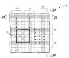
- FIG. 1is a diagrammatic top view of a substrate in process in accordance with an embodiment of the invention.
- FIG. 2is a cross sectional view taken through line 2 - 2 in FIG. 1 .
- FIG. 3is a cross sectional view taken through line 3 - 3 in FIG. 1 .
- FIG. 4is a view of the FIG. 1 substrate at a processing step subsequent to that shown by FIG. 1 .
- FIG. 5is a cross sectional view taken through line 5 - 5 in FIG. 4 .
- FIG. 6is a cross sectional view taken through line 6 - 6 in FIG. 4 .
- FIG. 7is a view of the FIG. 4 substrate at a processing step subsequent to that shown by FIG. 4 .
- FIG. 8is a cross sectional view taken through line 8 - 8 in FIG. 7 .
- FIG. 9is a cross sectional view taken through line 9 - 9 in FIG. 7 .
- FIG. 10is a view of the FIG. 7 substrate at a processing step subsequent to that shown by FIG. 7 .
- FIG. 11is a cross sectional view taken through line 11 - 11 in FIG. 10 .
- FIG. 12is a cross sectional view taken through line 12 - 12 in FIG. 10 .
- FIG. 13is a view of the FIG. 10 substrate at a processing step subsequent to that shown by FIG. 10 .
- FIG. 14is a cross sectional view taken through line 14 - 14 in FIG. 13 .
- FIG. 15is a cross sectional view taken through line 15 - 15 in FIG. 13 .
- FIG. 16is a view of the FIG. 13 substrate at a processing step subsequent to that shown by FIG. 13 .
- FIG. 17is a cross sectional view taken through line 17 - 17 in FIG. 16 .
- FIG. 18is a cross sectional view taken through line 18 - 18 in FIG. 16 .
- FIG. 19is a view of the FIG. 16 substrate at a processing step subsequent to that shown by FIG. 16 .
- FIG. 20is a cross sectional view taken through line 20 - 20 in FIG. 19 .
- FIG. 21is a cross sectional view taken through line 21 - 21 in FIG. 19 .
- FIG. 22is a view of the FIG. 19 substrate at a processing step subsequent to that shown by FIG. 19 .
- FIG. 23is a cross sectional view taken through line 23 - 23 in FIG. 22 .
- FIG. 24is a cross sectional view taken through line 24 - 24 in FIG. 22 .
- FIG. 25is a view of the FIG. 22 substrate at a processing step subsequent to that shown by FIG. 22 .
- FIG. 26is a cross sectional view taken through line 26 - 26 in FIG. 25 .
- FIG. 27is a cross sectional view taken through line 27 - 27 in FIG. 25 .
- FIG. 28is a view of the FIG. 25 substrate at a processing step subsequent to that shown by FIG. 25 .
- FIG. 29is a cross sectional view taken through line 29 - 29 in FIG. 28 .
- FIG. 30is a cross sectional view taken through line 30 - 30 in FIG. 28 .
- FIG. 31is a diagrammatic top view of a substrate in process in accordance with an embodiment of the invention.
- FIG. 32is a cross sectional view taken through line 32 - 32 in FIG. 31 .
- FIG. 33is a cross sectional view taken through line 33 - 33 in FIG. 31 .
- FIG. 34is a view of the FIG. 31 substrate at a processing step subsequent to that shown by FIG. 31 .
- FIG. 35is a cross sectional view taken through line 35 - 35 in FIG. 34 .
- FIG. 36is a cross sectional view taken through line 36 - 36 in FIG. 34 .
- FIG. 37is a diagrammatic top view of a substrate in process in accordance with an embodiment of the invention.
- FIG. 38is a cross sectional view taken through line 38 - 38 in FIG. 37 .
- FIG. 39is a cross sectional view taken through line 39 - 39 in FIG. 37 .
- FIG. 40is a diagrammatic top view of a substrate in process in accordance with an embodiment of the invention.
- FIG. 41is a cross sectional view taken through line 41 - 41 in FIG. 40 .
- FIG. 42is a cross sectional view taken through line 42 - 42 in FIG. 40 .
- FIG. 43is a view of the FIG. 40 substrate at a processing step subsequent to that shown by FIG. 40 .
- FIG. 44is a cross sectional view taken through line 44 - 44 in FIG. 43 .
- FIG. 45is a cross sectional view taken through line 45 - 45 in FIG. 43 .
- FIG. 46is a diagrammatic cross sectional view of an alternate substrate to that of FIG. 29 which is in process in accordance with an embodiment of the invention.
- FIG. 47is view of the FIG. 46 substrate corresponding in cross sectional cut location to that of FIG. 30 .
- FIG. 48is a view the FIG. 46 substrate at a processing step subsequent to that shown by FIG. 46 .
- FIG. 49is a view the FIG. 47 substrate at a processing step subsequent to that shown by FIG. 47 .
- FIG. 50is a diagrammatic top view of the FIGS. 48 and 49 substrate at a processing step subsequent to that shown by FIGS. 48 and 49 .
- FIG. 51is a cross sectional view taken through line 51 - 51 in FIG. 50 .
- FIG. 52is a cross sectional view taken through line 52 - 52 in FIG. 50 .
- first lines 12have been formed over an underlying substrate 14 .
- First lines 12may be homogenous or non-homogenous, may remain or be removed at the finish of processing, and may comprise any material, whether conductive, insulative, and/or semiconductive. Such may respectively have constant lateral width or variable width, and such may be of the same or different width, sizes and shapes relative one another. Further and regardless, such may be fabricated at, above, or below minimum photolithographic feature width where photolithography may be used during fabrication.
- One example material for first lines 12is photoresist.
- Underlying substrate 14may be homogenous or non-homogenous, for example comprising multiple different composition materials and/or layers.
- suchmay comprise bulk monocrystalline silicon and/or a semiconductor-on-insulator substrate.
- suchmay comprise dielectric material having conductive contacts or vias therein which extend vertically or otherwise into current conductive electrical connection with electronic device components, regions, or material received elevationally inward of the dielectric material.
- Underlying substrate 14may or may not be a semiconductor substrate.
- semiconductor substrateor “semiconductive substrate” is defined to mean any construction comprising semiconductive material, including, but not limited to, bulk semiconductive materials such as a semiconductive wafer (either alone or in assemblies comprising other materials thereon), and semiconductive material layers (either alone or in assemblies comprising other materials).
- substraterefers to any supporting structure, including, but not limited to, the semiconductive substrates described above.
- first lines 12may be or may have been subjected to a lateral trimming etch. Further and regardless, features 12 may have resulted from a pattern transfer from an overlying layer, followed by removal thereof.
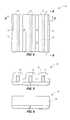
- a spacer-forming layer 16has been formed over first lines 12 .
- Suchmay be homogenous or non-homogenous, may be sacrificial, and may be formed by any suitable deposition technique.
- An example ideal techniqueis atomic layer deposition, and example compositions include silicon dioxide and silicon nitride.
- spacer-forming layer 16has been deposited to a thickness about equal to the lateral width of first lines 12 .
- spacer-forming layer 16has been subjected to an anisotropic etch, thereby forming first sidewall spacers 18 which are received longitudinally along opposite sides of first lines 12 .
- Suchmay be formed by masked and/or mask-less manner(s).
- Example first features 20are thereby formed elevationally over an underlying substrate, with such first features comprising longitudinally elongated first lines having first sidewall spacers (i.e., material extending or originally formed extending from sidewalls of another material) received longitudinally along opposite sides thereof. Any alternate existing or yet-to-be-developed technique(s) may be used to form first features 20 .
- Elevationally outermost surfaces 21 of the respective first sidewall spacersmay be elevationally coincident.
- Elevationally outermost surfaces 25 of the respective first linesmay be elevationally coincident. If the outermost surfaces of the first sidewall spacers and the first lines are respectively elevationally coincident, such may further be elevationally coincident relative each other.
- first fill material 22has been formed to be received laterally between first sidewall spacers 18 of laterally adjacent first features 20 .
- Suchmay be homogenous or non-homogenous, and may be of the same composition as the material of first lines 12 .
- Suchmay be organic and/or inorganic, and be deposited by any technique including liquid spin-on techniques which may inherently result in a planar elevationally outermost surface 23 .
- some suitable materialsinclude photoresist, spin-on materials, and antireflective coatings such as DARC and BARC.
- first fill material 22may or may not be planar, and may be formed to be elevationally coincident with, elevationally outward of, or inwardly of outermost surfaces 21 , 25 of first spacers 18 and/or first lines 12 .
- FIGS. 10-12depict an example wherein outermost surface 23 of first fill material 22 is elevationally outward of such surfaces of first spacers 18 and such surfaces of first lines 12 .
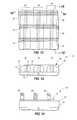
- longitudinally elongated second lines 24have been formed elevationally over first fill material 22 .
- Suchmay be of the same or different composition(s) as first lines 12 , and formed by any of the same or different techniques as described above.
- pitch-doubling process shownsuch have been formed to have a maximum lateral width equal to about the final feature width, with immediately adjacent second lines 24 being separated by spaces having about three times such final feature width.
- Alternate sizesmay be used, and the size and spacing of the first and second lines may not be the same (not shown).
- another spacer-forming layer 26has been formed over second lines 24 .
- Suchmay be of the same or different composition(s) as material of first spacers 18 .
- Suchis shown as having been deposited to about the minimum final feature width, although other thicknesses may be used.
- spacer-forming layer 26has been anisotropically etched to form second sidewall spacers 28 which are received longitudinally along opposite sides of second lines 24 . Such may be conducted in masked and/or mask-less manner(s).
- second features 30have been formed elevationally over and crossing first features 20 , with second features 30 comprising second lines 24 having sidewall spacers 28 received longitudinally along opposite sides thereof.
- first features 20 and second features 30cross orthogonally relative one another, although such may cross non-orthogonally.
- first features 20 and second features 30each extend longitudinally straight linear.
- one or both of the collective first features and the collective second featuresmay not be straight linear or respectively extend longitudinally curvilinear (not shown) regardless of whether crossing orthogonally relative one another.
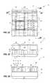
- second fill material 32is provided to be received laterally between second sidewall spacers 28 of laterally adjacent second features 30 .
- Suchmay be of the same or different composition(s) as first fill material 22 . Further, such may have any of the same attributes described above with respect to first fill material 22 , including by way of example only those with respect to the second spacers and second lines as the first fill material may have with respect to the first spacers and first lines.
- second fill material 32has been removed sufficiently to at least expose elevationally outermost surfaces of second sidewall spacers 28 (not shown), with such spacers thereafter having been removed.
- the act of removing the second sidewall spacersmay or may not expose underlying first sidewall spacers 18 , with such not being exposed in FIGS. 25 and 26 due to first fill material 22 being received thereover.
- removal of the second sidewall spacers from between the second lines and the second fill materialis conducted by a selective anisotropic etch.
- a “selective etch”denotes removal of one material relative to another at a removal rate of at least 1.5:1.
- first fill material 22has been removed at least where covering underlying first sidewall spacers 18 and first lines 12 . Subsequently, portions of first sidewall spacers 18 (not shown) have been removed from between first lines 12 and first fill material 22 that are not covered by second lines 24 and second fill material 32 . Such may be conducted ideally by a selective anisotropic etch relative to the first lines, the first fill material, the second lines, and the second fill material. Regardless, FIGS. 28-30 show an example pattern 35 comprising a plurality of openings 45 .
- first fill material 22was formed to have an elevationally outer surface that was elevationally outward of elevationally outermost surfaces 21 of first sidewall spacers 18 (see FIGS. 10-12 ).
- FIGS. 31-33show first fill material 22 as having been formed to have its elevationally outermost surface 23 to be elevationally coincident with elevationally outermost surfaces 21 of first sidewall spacers 18 ( FIG. 32 ). Additionally, surface 23 is elevationally coincident with first line outer surfaces 25 . Further, outermost surfaces 21 of first sidewall spacers 18 are at a common elevation “E”, with elevationally outermost surface 23 of first fill material 22 being planar and elevationally coincident with outermost surfaces 21 of first sidewall spacers 18 .
- FIGS. 34-36correspond in processing sequence to FIGS. 25-27 of the first-described embodiments.
- Second sidewall spacers 28(not shown) have been removed from between second lines 24 and second fill material 32 whereby underlying portions of first sidewall spacers 18 have been exposed. Such removal has exposed only some of the lateral width “W” of respective first sidewall spacers 18 due to, for example, the depicted upper surfaces of first spacers 18 curving or tapering laterally outward and elevationally inward.
- FIGS. 37-39correspond in processing sequence as would occur immediately subsequent to that of FIGS. 10-12 or FIGS. 31-32 in the above-described embodiments.
- first lines 12 , first sidewall spacers 18 , and first fill material 22have been planarized elevationally inward to a co-planar elevationally outermost surface T. Processing may occur subsequently in any of the manners described above.
- first sidewall spacers 18may inherently expose portions of first sidewall spacers 18 .
- a material or structureis “directly against” another when there is at least some physical touching contact of the stated materials or structures relative one another.
- “over”encompasses “directly against” as well as constructions where intervening material(s) or structure(s) result(s) in no physical touching contact of the stated materials or structures relative one another.
- FIGS. 40-45Another example embodiment of a method of forming a pattern on a substrate is described with reference to FIGS. 40-45 with respect to a substrate fragment 10 c .
- Like numerals from the above-described embodimentshave been used.
- original first lines 12remain prior to deposition of first fill material 22 .
- some or all of such original line materialmay be removed.
- FIGS. 7-9may be considered as depicting formation of spaced longitudinally elongated lines 12 having first sidewall spacers 18 formed longitudinally along sidewalls thereof.
- FIGS. 40-42show removal of such spaced lines (not shown) from between first sidewall spacers 18 .
- first fill material 22has been deposited over first sidewall spacers 18 , laterally between first sidewall spacers 18 where the removed spaced lines (not shown) were, and laterally between first sidewall spacers 18 of laterally adjacent first features 20 .
- first materialmay be planarized back to at least the elevationally outermost surfaces of the first spacers, or further elevationally inward to provide a co-planar elevationally outermost surface of the first lines, first sidewall spacers, and first fill material. Regardless, processing may occur subsequently in any of the example manners described above, or otherwise.
- formation of the second featuresmay comprise forming spaced longitudinally elongated lines having second sidewall spacers received longitudinally along sidewalls thereof. Some or all of such spaced lines may be removed from between the second sidewall spacers. Thereafter, second fill material may be deposit over the second sidewall spacers, laterally between the second sidewall spacers where the removed space lines were, and laterally between the second sidewall spacers of laterally adjacent second features.
- Integrated circuitry components and/or other structuresmay be formed using, or may comprise, some or all of example pattern 35 ( FIGS. 28-30 ) formed on a substrate. Alternately or additionally, such pattern may be used as a mask for subsequent processing of substrate material there-beneath.
- the underlying substratemay be etched into using remnant of the first and second features and the first and second fill materials as a mask.
- a plurality of contact openingsare formed which extend to node locations in the underlying substrate.
- FIGS. 46-52show a substrate fragment 10 d the same as that of FIGS.
- first features 20 , of second features 30 , of first fill material 22 , and of second fill material 32may be considered as comprising an example first mask.
- such first maskhas been used to form a contact opening pattern into hardmask material 40 by etching through openings in such first mask. Some, all, or none of the first mask may remain after the etching to form the depicted contact opening pattern in hardmask material 40 . Further if any is remaining, such may be removed subsequently.
- a plurality of contact openings 55has been etched into substrate material 42 using the contact opening pattern in hardmask material 40 as a second mask. Some, all, or none of the first mask (not shown) may remain after the FIGS. 50-52 etching if any remained over material 40 at the start of the FIGS. 50-52 etching.
- a method of forming a pattern on a substrateincludes forming anisotropically etched first sidewall spacers elevationally over an underlying substrate.
- the above-described processing through FIG. 9is but one example embodiment, and regardless of material or structure being received between first sidewall spacers 18 .
- Anisotropically etched second sidewall spacersare formed elevationally over and cross the first sidewall spacers, and regardless of whether material is received between the first sidewall spacers when the anisotropically etched second spacers are formed. Intersections of the first and second sidewall spacers define respective elevationally overlapped areas of the first sidewall spacers where the second sidewall spacers cross over the first sidewall spacers. Processing as described above is but one such example embodiment wherein such example elevationally overlapped areas are designated with arrows 75 in the FIG. 19 embodiment, and regardless of whether material or structure is received between any of the first sidewall spacers or any of the second sidewall spacers.
- the second sidewall spacersare removed where such cross over the first sidewall spacers and the overlapped areas of the first sidewall spacers are exposed. Such occurs regardless of the presence of fill or other material between any of the first and second sidewall spacers. Further, the removal of the second sidewall spacers may remove all of such or only some of such from the substrate. Regardless, material of the first sidewall spacers is removed through the exposed overlapped areas to the underlying substrate while at least a majority of the area of the first sidewall spacers outside of the overlapped areas is masked. By way of example only, FIGS. 28-30 show example such removal of material of first sidewall spacers 18 (not shown). Alternate and/or additional processing may otherwise occur as described above.
- the second sidewall spacersmay be formed directly against the first sidewall spacers, and the act of removing of the second sidewall spacers may inherently expose the overlapped areas of the first sidewall spacers.
- the second sidewall spacersmay not be formed directly against the first sidewall spacers, and the removing of the second sidewall spacers may not in such instance expose the overlapped areas of the first sidewall spacers.
- the elevationally outermost surfaces of the first sidewall spacersmay initially be non-planar as formed. Such may subsequently be planarized prior to forming the second sidewall spacers.
- a method of forming a pattern on a substrateincludes forming a repeating pattern of four first lines elevationally over an underlying substrate.
- four example first lines A, B, C, and Dare shown in FIGS. 10 , 11 , and 26 as an example repeating pattern formed over an underlying substrate.
- a repeating pattern of four second linesis formed elevationally over and cross the repeating pattern of four first lines.
- such example repeating four second lines E, F, G, and Hare shown in FIGS. 22 and 24 .
- First alternating ones of the four second linesare removed from being received over the first lines.
- alternating second lines F and Hconstitute such an example first alternating ones of such second lines which have been removed from being received over first lines A, B, C, and D.
- elevationally exposed portions of alternating ones of the four first linesare removed to the underlying substrate using a remaining second alternating of the four second lines as a mask.
- FIGS. 28-30depicts one such example embodiment.
- elevationally exposed portions of alternating first lines B and D (not shown) of the four first lines A, B, C, and Dhave been removed to underlying substrate 14 using a remaining second alternating ones E and G of the four second lines as a mask. Any alternate and/or additional processing as described above may be used.
- a method of forming a pattern on a substrateincludes forming first and second lines elevationally over an underlying substrate.
- an immediately adjacent pair of two lines A in FIG. 10constitute but example such first and second lines.
- Third and fourth linesare formed elevationally over and cross the first and second lines; with the first, second, third, and fourth lines forming a quadrilateral there-between.
- any immediately adjacent pair of two lines Econstitutes an example such third and fourth lines which have been formed elevationally over and cross first lines A, A.
- An example quadrilateral Qis shown formed between/among such crossing lines. Any quadrilateral may be formed, including parallelograms, trapezoids, rectangles, squares, etc., with a square Q being shown in FIG. 22 .
- a pair of crossing linesis provided within the quadrilateral.
- lines C and G formed thereinconstitutes an example pair of crossing lines.
- Such linesmay be centered within the quadrilateral, otherwise positioned within the quadrilateral, and/or need not cross orthogonally relative one another.
- the first, second, third, fourth, and the pair of crossing linesare used as a mask while etching through material to form a pattern of four openings which are individually received within a respective different one of four corners of the quadrilateral.
- an example four openings 45FIG. 28
- FIG. 28an example four openings 45 are shown with respect to a quadrilateral Q and which are individually received within a respective different one of the four corners of such.
Landscapes
- Engineering & Computer Science (AREA)
- Physics & Mathematics (AREA)
- Condensed Matter Physics & Semiconductors (AREA)
- General Physics & Mathematics (AREA)
- Manufacturing & Machinery (AREA)
- Computer Hardware Design (AREA)
- Microelectronics & Electronic Packaging (AREA)
- Power Engineering (AREA)
- Chemical & Material Sciences (AREA)
- Inorganic Chemistry (AREA)
- Internal Circuitry In Semiconductor Integrated Circuit Devices (AREA)
Abstract
Description
Claims (35)
Priority Applications (2)
| Application Number | Priority Date | Filing Date | Title |
|---|---|---|---|
| US13/101,485US8575032B2 (en) | 2011-05-05 | 2011-05-05 | Methods of forming a pattern on a substrate |
| US14/064,261US9153458B2 (en) | 2011-05-05 | 2013-10-28 | Methods of forming a pattern on a substrate |
Applications Claiming Priority (1)
| Application Number | Priority Date | Filing Date | Title |
|---|---|---|---|
| US13/101,485US8575032B2 (en) | 2011-05-05 | 2011-05-05 | Methods of forming a pattern on a substrate |
Related Child Applications (1)
| Application Number | Title | Priority Date | Filing Date |
|---|---|---|---|
| US14/064,261ContinuationUS9153458B2 (en) | 2011-05-05 | 2013-10-28 | Methods of forming a pattern on a substrate |
Publications (2)
| Publication Number | Publication Date |
|---|---|
| US20120282778A1 US20120282778A1 (en) | 2012-11-08 |
| US8575032B2true US8575032B2 (en) | 2013-11-05 |
Family
ID=47090499
Family Applications (2)
| Application Number | Title | Priority Date | Filing Date |
|---|---|---|---|
| US13/101,485Active2031-05-20US8575032B2 (en) | 2011-05-05 | 2011-05-05 | Methods of forming a pattern on a substrate |
| US14/064,261ActiveUS9153458B2 (en) | 2011-05-05 | 2013-10-28 | Methods of forming a pattern on a substrate |
Family Applications After (1)
| Application Number | Title | Priority Date | Filing Date |
|---|---|---|---|
| US14/064,261ActiveUS9153458B2 (en) | 2011-05-05 | 2013-10-28 | Methods of forming a pattern on a substrate |
Country Status (1)
| Country | Link |
|---|---|
| US (2) | US8575032B2 (en) |
Cited By (7)
| Publication number | Priority date | Publication date | Assignee | Title |
|---|---|---|---|---|
| US20140051251A1 (en)* | 2011-05-05 | 2014-02-20 | Micron Technology, Inc. | Methods Of Forming a Pattern on a Substrate |
| US20150108619A1 (en)* | 2013-10-21 | 2015-04-23 | Applied Materials, Inc. | Method for patterning a semiconductor substrate |
| US9305782B2 (en) | 2006-07-10 | 2016-04-05 | Micron Technology, Inc. | Pitch reduction technology using alternating spacer depositions during the formation of a semiconductor device and systems including same |
| US9330934B2 (en) | 2009-05-18 | 2016-05-03 | Micron Technology, Inc. | Methods of forming patterns on substrates |
| US10151981B2 (en) | 2008-05-22 | 2018-12-11 | Micron Technology, Inc. | Methods of forming structures supported by semiconductor substrates |
| US10460938B2 (en) | 2016-04-14 | 2019-10-29 | Tokyo Electron Limited | Method for patterning a substrate using a layer with multiple materials |
| US11195997B2 (en) | 2019-07-23 | 2021-12-07 | Samsung Electronics Co., Ltd. | Variable resistance memory devices including self-heating layer and methods of manufacturing the same |
Families Citing this family (10)
| Publication number | Priority date | Publication date | Assignee | Title |
|---|---|---|---|---|
| KR20120126228A (en)* | 2011-05-11 | 2012-11-21 | 삼성전자주식회사 | Methods of forming a pattern and methods of manufacturing a semiconductor device using the same |
| US8716133B2 (en)* | 2012-08-23 | 2014-05-06 | International Business Machines Corporation | Three photomask sidewall image transfer method |
| US9070559B2 (en)* | 2013-07-25 | 2015-06-30 | Kabushiki Kaisha Toshiba | Pattern forming method and method of manufacturing semiconductor device |
| US9177797B2 (en)* | 2013-12-04 | 2015-11-03 | Taiwan Semiconductor Manufacturing Company, Ltd. | Lithography using high selectivity spacers for pitch reduction |
| SG11201806451VA (en) | 2016-01-29 | 2018-08-30 | Tokyo Electron Ltd | Method and system for forming memory fin patterns |
| US9882028B2 (en)* | 2016-06-29 | 2018-01-30 | International Business Machines Corporation | Pitch split patterning for semiconductor devices |
| US10388644B2 (en) | 2016-11-29 | 2019-08-20 | Taiwan Semiconductor Manufacturing Company, Ltd. | Method of manufacturing conductors and semiconductor device which includes conductors |
| US10217633B2 (en)* | 2017-03-13 | 2019-02-26 | Globalfoundries Inc. | Substantially defect-free polysilicon gate arrays |
| US10763262B2 (en)* | 2018-11-23 | 2020-09-01 | Nanya Technology Corporation | Method of preparing semiconductor structure |
| US11049721B2 (en)* | 2019-07-31 | 2021-06-29 | Tokyo Electron Limited | Method and process for forming memory hole patterns |
Citations (211)
| Publication number | Priority date | Publication date | Assignee | Title |
|---|---|---|---|---|
| EP0171111A3 (en) | 1984-07-13 | 1987-07-22 | BELL TELEPHONE MANUFACTURING COMPANY Naamloze Vennootschap | Process to superpose two positive photoresist layers |
| US4910168A (en) | 1988-05-06 | 1990-03-20 | Mos Electronics Corporation | Method to reduce silicon area for via formation |
| US5008207A (en) | 1989-09-11 | 1991-04-16 | International Business Machines Corporation | Method of fabricating a narrow base transistor |
| US5047117A (en) | 1990-09-26 | 1991-09-10 | Micron Technology, Inc. | Method of forming a narrow self-aligned, annular opening in a masking layer |
| US5254218A (en) | 1992-04-22 | 1993-10-19 | Micron Technology, Inc. | Masking layer having narrow isolated spacings and the method for forming said masking layer and the method for forming narrow isolated trenches defined by said masking layer |
| US5328810A (en) | 1990-05-07 | 1994-07-12 | Micron Technology, Inc. | Method for reducing, by a factor or 2-N, the minimum masking pitch of a photolithographic process |
| US5372916A (en) | 1991-09-12 | 1994-12-13 | Hitachi, Ltd. | X-ray exposure method with an X-ray mask comprising phase shifter sidewalls |
| US5382315A (en) | 1991-02-11 | 1995-01-17 | Microelectronics And Computer Technology Corporation | Method of forming etch mask using particle beam deposition |
| US5420067A (en) | 1990-09-28 | 1995-05-30 | The United States Of America As Represented By The Secretary Of The Navy | Method of fabricatring sub-half-micron trenches and holes |
| US5429988A (en) | 1994-06-13 | 1995-07-04 | United Microelectronics Corporation | Process for producing high density conductive lines |
| US5573837A (en) | 1992-04-22 | 1996-11-12 | Micron Technology, Inc. | Masking layer having narrow isolated spacings and the method for forming said masking layer and the method for forming narrow isolated trenches defined by said masking layer |
| US5593813A (en) | 1994-07-14 | 1997-01-14 | Hyundai Electronics Industries Co. Ltd. | Method for forming submicroscopic patterns |
| US5616510A (en) | 1992-11-02 | 1997-04-01 | Wong; Chun C. D. | Method for making multimedia storage system with highly compact memory cells |
| US5905279A (en) | 1996-04-09 | 1999-05-18 | Kabushiki Kaisha Toshiba | Low resistant trench fill for a semiconductor device |
| US6063688A (en) | 1997-09-29 | 2000-05-16 | Intel Corporation | Fabrication of deep submicron structures and quantum wire transistors using hard-mask transistor width definition |
| US6087263A (en) | 1998-01-29 | 2000-07-11 | Micron Technology, Inc. | Methods of forming integrated circuitry and integrated circuitry structures |
| US6140217A (en) | 1998-07-16 | 2000-10-31 | International Business Machines Corporation | Technique for extending the limits of photolithography |
| US6207490B1 (en) | 1997-12-11 | 2001-03-27 | Samsung Electronics Co., Ltd. | Semiconductor device and method for fabricating the same |
| US6235574B1 (en) | 1999-03-22 | 2001-05-22 | Infineon North America Corp. | High performance DRAM and method of manufacture |
| US6249335B1 (en) | 1992-01-17 | 2001-06-19 | Nikon Corporation | Photo-mask and method of exposing and projection-exposing apparatus |
| US6303272B1 (en) | 1998-11-13 | 2001-10-16 | International Business Machines Corporation | Process for self-alignment of sub-critical contacts to wiring |
| US20020037617A1 (en) | 2000-06-29 | 2002-03-28 | Kim Jun Dong | Method for forming gate electrodes in a semicoductor device using formed fine patterns |
| JP3270227B2 (en) | 1993-05-26 | 2002-04-02 | 富士写真フイルム株式会社 | Electric hoist |
| US6383952B1 (en) | 2001-02-28 | 2002-05-07 | Advanced Micro Devices, Inc. | RELACS process to double the frequency or pitch of small feature formation |
| US20020094688A1 (en) | 2001-01-16 | 2002-07-18 | Semiconductor Leading Edge Technologies, Inc. | Method of forming fine patterns |
| US6429123B1 (en) | 2000-10-04 | 2002-08-06 | Vanguard International Semiconductor Corporation | Method of manufacturing buried metal lines having ultra fine features |
| US6483136B1 (en) | 1997-06-20 | 2002-11-19 | Hitachi, Ltd. | Semiconductor integrated circuit and method of fabricating the same |
| EP1273974A2 (en) | 2001-07-05 | 2003-01-08 | Tokyo Ohka Kogyo Co., Ltd. | Method for reducing a pattern dimension in a photoresist layer |
| US20030006410A1 (en) | 2000-03-01 | 2003-01-09 | Brian Doyle | Quantum wire gate device and method of making same |
| US6545904B2 (en) | 2001-03-16 | 2003-04-08 | Micron Technology, Inc. | 6f2 dram array, a dram array formed on a semiconductive substrate, a method of forming memory cells in a 6f2 dram array and a method of isolating a single row of memory cells in a 6f2 dram array |
| US6548401B1 (en) | 2002-01-23 | 2003-04-15 | Micron Technology, Inc. | Semiconductor processing methods, and semiconductor constructions |
| US6548385B1 (en) | 2002-06-12 | 2003-04-15 | Jiun-Ren Lai | Method for reducing pitch between conductive features, and structure formed using the method |
| US20030091936A1 (en) | 2001-08-31 | 2003-05-15 | Jorg Rottstegge | Process for sidewall amplification of resist structures and for the production of structures having reduced structure size |
| US6566280B1 (en) | 2002-08-26 | 2003-05-20 | Intel Corporation | Forming polymer features on a substrate |
| US6580136B2 (en) | 2001-01-30 | 2003-06-17 | International Business Machines Corporation | Method for delineation of eDRAM support device notched gate |
| KR20030049198A (en) | 2001-12-14 | 2003-06-25 | 주식회사 하이닉스반도체 | Forming method of photoresist pattern improving etching resistance by relacs material |
| KR20030056601A (en) | 2001-12-28 | 2003-07-04 | 주식회사 하이닉스반도체 | Method of forming a source line in flash memory device |
| US6599844B2 (en) | 2000-06-22 | 2003-07-29 | Hyundai Electronics Industries, Co., Ltd. | Method and forming fine patterns of semiconductor devices using passivation layers |
| US6605541B1 (en) | 1998-05-07 | 2003-08-12 | Advanced Micro Devices, Inc. | Pitch reduction using a set of offset masks |
| JP2003234279A (en) | 2002-02-08 | 2003-08-22 | Sony Corp | Forming method of resist pattern, manufacturing method of semiconductor device and forming device for resist pattern |
| US6627524B2 (en) | 2001-06-06 | 2003-09-30 | Micron Technology, Inc. | Methods of forming transistor gates; and methods of forming programmable read-only memory constructions |
| US6630379B2 (en) | 2000-06-23 | 2003-10-07 | International Business Machines Corporation | Method of manufacturing 6F2 trench capacitor DRAM cell having vertical MOSFET and 3F bitline pitch |
| US6638441B2 (en) | 2002-01-07 | 2003-10-28 | Macronix International Co., Ltd. | Method for pitch reduction |
| KR20030089063A (en) | 2002-05-16 | 2003-11-21 | 주식회사 하이닉스반도체 | Forming method of photoresist pattern |
| US6667502B1 (en) | 1999-08-31 | 2003-12-23 | Micron Technology, Inc. | Structurally-stabilized capacitors and method of making of same |
| US6703323B2 (en) | 2001-12-14 | 2004-03-09 | Hynix Semiconductor Inc | Method of inhibiting pattern collapse using a relacs material |
| US6710390B2 (en) | 1997-07-03 | 2004-03-23 | Micron Technology, Inc. | Capacitors and DRAM arrays |
| JP2004134574A (en) | 2002-10-10 | 2004-04-30 | Renesas Technology Corp | Manufacturing method of semiconductor device |
| US6735132B2 (en) | 2001-07-23 | 2004-05-11 | Micron Technology, Inc. | 6F2 DRAM array with apparatus for stress testing an isolation gate and method |
| US6753220B2 (en) | 1996-11-01 | 2004-06-22 | Micron Technology, Inc. | Semiconductor processing methods of forming devices on a substrate, forming device arrays on a substrate, forming conductive lines on a substrate, and forming capacitor arrays on a substrate, and integrated circuitry |
| US6756619B2 (en) | 2002-08-26 | 2004-06-29 | Micron Technology, Inc. | Semiconductor constructions |
| KR20040057582A (en) | 2002-12-26 | 2004-07-02 | 주식회사 하이닉스반도체 | Method of forming a micro pattern having a dual damascene |
| JP2004247399A (en) | 2003-02-12 | 2004-09-02 | Renesas Technology Corp | Method for manufacturing semiconductor device |
| US20040198065A1 (en) | 2003-04-04 | 2004-10-07 | Sung-Kwon Lee | Method for fabricating semiconductor device with fine patterns |
| US6826069B2 (en) | 2001-03-14 | 2004-11-30 | Atmos Corporation | Interleaved wordline architecture |
| US20040253535A1 (en) | 2002-11-20 | 2004-12-16 | Shipley Company, L.L.C. | Multilayer photoresist systems |
| US6864184B1 (en) | 2004-02-05 | 2005-03-08 | Advanced Micro Devices, Inc. | Method for reducing critical dimension attainable via the use of an organic conforming layer |
| US6872512B2 (en) | 2002-03-27 | 2005-03-29 | Nec Lcd Technologies, Ltd. | Method of forming resist pattern |
| US6905975B2 (en) | 2003-07-03 | 2005-06-14 | Micron Technology, Inc. | Methods of forming patterned compositions |
| US20050130068A1 (en) | 2003-11-21 | 2005-06-16 | Takehiro Kondoh | Pattern forming method and method for manufacturing a semiconductor device |
| US20050142497A1 (en) | 2003-12-26 | 2005-06-30 | Samsung Electronics Co., Ltd. | Method of forming a pattern in a semiconductor device and method of forming a gate using the same |
| US6916594B2 (en) | 2002-12-30 | 2005-07-12 | Hynix Semiconductor Inc. | Overcoating composition for photoresist and method for forming photoresist pattern using the same |
| US20050164478A1 (en) | 2004-01-26 | 2005-07-28 | Taiwan Semiconductor Manufacturing Co. | Novel method of trimming technology |
| US20050173740A1 (en) | 2004-02-07 | 2005-08-11 | You-Seung Jin | Multi-gate transistor formed with active patterns of uniform critical dimension |
| JP2005243681A (en) | 2004-02-24 | 2005-09-08 | Tokyo Electron Ltd | Film modifying method, film modifying apparatus and control method of amount of slimming |
| US6951822B2 (en) | 2001-09-28 | 2005-10-04 | Infineon Technologies North America Corp. | Method for forming inside nitride spacer for deep trench device DRAM cell |
| US20050255696A1 (en) | 2003-05-09 | 2005-11-17 | Fujitsu Limited | Method of processing resist, semiconductor device, and method of producing the same |
| US20050272220A1 (en) | 2004-06-07 | 2005-12-08 | Carlo Waldfried | Ultraviolet curing process for spin-on dielectric materials used in pre-metal and/or shallow trench isolation applications |
| US20060011947A1 (en) | 2004-05-26 | 2006-01-19 | Werner Juengling | Semiconductor structures and memory device constructions |
| US20060024621A1 (en) | 2004-07-17 | 2006-02-02 | Infineon Technologies Ag | Method of producing a structure on the surface of a substrate |
| US20060046422A1 (en) | 2004-08-31 | 2006-03-02 | Micron Technology, Inc. | Methods for increasing photo alignment margins |
| US20060046200A1 (en) | 2004-09-01 | 2006-03-02 | Abatchev Mirzafer K | Mask material conversion |
| US20060046484A1 (en) | 2004-09-02 | 2006-03-02 | Abatchev Mirzafer K | Method for integrated circuit fabrication using pitch multiplication |
| US20060063384A1 (en) | 2004-09-23 | 2006-03-23 | Jung-Hwan Hah | Mask patterns for semiconductor device fabrication and related methods and structures |
| US7023069B2 (en) | 2003-12-19 | 2006-04-04 | Third Dimension (3D) Semiconductor, Inc. | Method for forming thick dielectric regions using etched trenches |
| CN1761063A (en) | 2004-10-14 | 2006-04-19 | 茂德科技股份有限公司 | Structure of Dynamic Random Access Memory |
| US20060088788A1 (en) | 2004-10-26 | 2006-04-27 | Takanori Kudo | Composition for coating over a photoresist pattern |
| US7037840B2 (en) | 2004-01-26 | 2006-05-02 | Micron Technology, Inc. | Methods of forming planarized surfaces over semiconductor substrates |
| US7049652B2 (en) | 2003-12-10 | 2006-05-23 | Sandisk Corporation | Pillar cell flash memory technology |
| US20060115978A1 (en) | 2004-11-30 | 2006-06-01 | Michael Specht | Charge-trapping memory cell and method for production |
| US20060118785A1 (en) | 2003-09-12 | 2006-06-08 | International Business Machines Corporation | Techniques for patterning features in semiconductor devices |
| US7064376B2 (en) | 1996-05-24 | 2006-06-20 | Jeng-Jye Shau | High performance embedded semiconductor memory devices with multiple dimension first-level bit-lines |
| US7067385B2 (en) | 2003-09-04 | 2006-06-27 | Micron Technology, Inc. | Support for vertically oriented capacitors during the formation of a semiconductor device |
| US20060154182A1 (en) | 2005-01-12 | 2006-07-13 | International Business Machines Corporation | Method for post lithographic critical dimension shrinking using post overcoat planarization |
| JP2006245625A (en) | 1997-06-20 | 2006-09-14 | Hitachi Ltd | Semiconductor integrated circuit device and manufacturing method thereof |
| US7125781B2 (en) | 2003-09-04 | 2006-10-24 | Micron Technology, Inc. | Methods of forming capacitor devices |
| US20060240361A1 (en) | 2005-04-21 | 2006-10-26 | Ji-Young Lee | Method of forming small pitch pattern using double spacers |
| US20060263699A1 (en)* | 2005-05-23 | 2006-11-23 | Mirzafer Abatchev | Methods for forming arrays of a small, closely spaced features |
| US20060273456A1 (en) | 2005-06-02 | 2006-12-07 | Micron Technology, Inc., A Corporation | Multiple spacer steps for pitch multiplication |
| US20060278911A1 (en) | 2005-06-14 | 2006-12-14 | Eppich Anton P | Relaxed-pitch method of aligning active area to digit line |
| US20060286795A1 (en) | 2005-06-21 | 2006-12-21 | Kabushiki Kaisha Toshiba | Method of manufacturing semiconductor device |
| US20070003878A1 (en) | 2005-03-23 | 2007-01-04 | Asml Netherlands B.V. | Reduced pitch multiple exposure process |
| US20070010058A1 (en) | 2005-07-08 | 2007-01-11 | Micron Technology, Inc. | Method and apparatus for a self-aligned recessed access device (RAD) transistor gate |
| US7166533B2 (en) | 2005-04-08 | 2007-01-23 | Infineon Technologies, Ag | Phase change memory cell defined by a pattern shrink material process |
| US20070020565A1 (en) | 2005-07-25 | 2007-01-25 | Samsung Electronics Co., Ltd. | Methods of fabricating a semiconductor device |
| JP2007017993A (en) | 2006-08-22 | 2007-01-25 | Fujitsu Ltd | Resist pattern and method for manufacturing the same, and semiconductor device and method for manufacturing the same |
| US20070023805A1 (en) | 2005-07-26 | 2007-02-01 | Wells David H | Reverse construction memory cell |
| US20070026684A1 (en) | 2005-08-01 | 2007-02-01 | Stefano Parascandola | Method of producing pitch fractionizations in semiconductor technology |
| US20070037066A1 (en) | 2005-08-09 | 2007-02-15 | Li-Tung Hsiao | Method for correcting and configuring optical mask pattern |
| US20070049030A1 (en) | 2005-09-01 | 2007-03-01 | Sandhu Gurtej S | Pitch multiplication spacers and methods of forming the same |
| US20070045712A1 (en) | 2005-09-01 | 2007-03-01 | Haller Gordon A | Memory cell layout and process flow |
| US20070049003A1 (en) | 2005-09-01 | 2007-03-01 | John Smythe | Semiconductor constructions and methods of forming layers |
| US20070049040A1 (en) | 2005-03-15 | 2007-03-01 | Micron Technology, Inc., A Corporation | Multiple deposition for integration of spacers in pitch multiplication process |
| US20070048674A1 (en) | 2005-09-01 | 2007-03-01 | Wells David H | Methods for forming arrays of small, closely spaced features |
| US20070048930A1 (en) | 2005-09-01 | 2007-03-01 | Figura Thomas A | Peripheral gate stacks and recessed array gates |
| US20070049035A1 (en) | 2005-08-31 | 2007-03-01 | Tran Luan C | Method of forming pitch multipled contacts |
| US20070049011A1 (en) | 2005-09-01 | 2007-03-01 | Micron Technology, Inc., A Corporation | Method of forming isolated features using pitch multiplication |
| US7199005B2 (en) | 2005-08-02 | 2007-04-03 | Micron Technology, Inc. | Methods of forming pluralities of capacitors |
| US20070077524A1 (en) | 2005-09-30 | 2007-04-05 | Samsung Electronics Co., Ltd. | Method for forming patterns of semiconductor device |
| US20070077743A1 (en) | 2005-09-30 | 2007-04-05 | Rao Rajesh A | Multiple fin formation |
| US7202174B1 (en) | 2006-02-02 | 2007-04-10 | Hynix Semiconductor Inc. | Method of forming micro pattern in semiconductor device |
| US7202127B2 (en) | 2004-08-27 | 2007-04-10 | Micron Technology, Inc. | Methods of forming a plurality of capacitors |
| US20070085152A1 (en) | 2005-10-14 | 2007-04-19 | Promos Technologies Pte.Ltd. Singapore | Reduced area dynamic random access memory (DRAM) cell and method for fabricating the same |
| US20070096182A1 (en) | 2004-09-10 | 2007-05-03 | Infineon Technologies Ag | Transistor, meomory cell array and method of manufacturing a transistor |
| US20070099431A1 (en) | 2005-11-01 | 2007-05-03 | Micron Technology, Inc. | Process for increasing feature density during the manufacture of a semiconductor device |
| US20070105357A1 (en) | 2005-09-01 | 2007-05-10 | Micron Technology, Inc. | Silicided recessed silicon |
| US20070123015A1 (en) | 2005-11-30 | 2007-05-31 | International Business Machines Corporation | Passive components in the back end of integrated circuits |
| US7230292B2 (en) | 2003-08-05 | 2007-06-12 | Micron Technology, Inc. | Stud electrode and process for making same |
| US20070145464A1 (en) | 2002-08-29 | 2007-06-28 | Voshell Thomas W | Random access memory device utilizing a vertically oriented select transistor |
| US20070161251A1 (en) | 2005-03-15 | 2007-07-12 | Micron Technology, Inc. | Pitch reduced patterns relative to photolithography features |
| US20070181929A1 (en) | 2005-06-27 | 2007-08-09 | Micron Technology, Inc. | Semiconductor Constructions, Memory Cells, DRAM Arrays, Electronic Systems; Methods of Forming Semiconductor Constructions; and Methods of Forming DRAM Arrays |
| US20070190463A1 (en) | 2004-09-02 | 2007-08-16 | Micron Technology, Inc. | Method to align mask patterns |
| US20070197014A1 (en) | 2006-02-17 | 2007-08-23 | Samsung Electronics Co., Ltd. | Method of fabricating semiconductor device |
| CN101026087A (en) | 2006-02-24 | 2007-08-29 | 海力士半导体有限公司 | Method for forming fine pattern of semiconductor device |
| US20070202697A1 (en) | 2006-02-24 | 2007-08-30 | Hynix Semiconductor Inc. | Method for forming fine pattern of semiconductor device |
| US20070205443A1 (en) | 2006-03-02 | 2007-09-06 | Werner Juengling | Vertical gated access transistor |
| US20070205438A1 (en) | 2006-03-02 | 2007-09-06 | Werner Juengling | Masking process for simultaneously patterning separate regions |
| US20070224537A1 (en) | 2006-03-24 | 2007-09-27 | Fujitsu Limited | Resist composition, method for forming resist pattern, and semiconductor device and method for manufacturing the same |
| US20070238299A1 (en) | 2006-04-07 | 2007-10-11 | Micron Technology, Inc. | Simplified pitch doubling process flow |
| US20070238053A1 (en) | 2006-04-11 | 2007-10-11 | Koji Hashimoto | Manufacturing method of semiconductor device |
| US20070248916A1 (en) | 2006-04-21 | 2007-10-25 | Tdk Corporation | Resist pattern forming method, thin-film pattern forming method, and microdevice manufacturing method |
| US20070264830A1 (en) | 2006-05-10 | 2007-11-15 | Lam Research Corporation | Pitch reduction |
| US20070264828A1 (en) | 2006-05-09 | 2007-11-15 | Hynix Semiconductor Inc. | Method for forming fine pattern of semiconductor device |
| US20070281493A1 (en) | 2006-06-02 | 2007-12-06 | Janos Fucsko | Methods of shaping vertical single crystal silicon walls and resulting structures |
| US20070278183A1 (en) | 2006-06-02 | 2007-12-06 | Whonchee Lee | Wet etch suitable for creating square cuts in si and resulting structures |
| US20070281219A1 (en) | 2006-06-01 | 2007-12-06 | Sandhu Gurtej S | Masking techniques and contact imprint reticles for dense semiconductor fabrication |
| US20070281488A1 (en) | 2006-06-02 | 2007-12-06 | Wells David H | Methods of fabricating intermediate semiconductor structures by selectively etching pockets of implanted silicon |
| KR100784062B1 (en) | 2006-01-20 | 2007-12-10 | 주식회사 하이닉스반도체 | Method of forming fine pattern of semiconductor device |
| US20080002475A1 (en) | 2006-06-29 | 2008-01-03 | Samsung Electronics Co., Ltd | Non-volatile memory devices having a vertical channel and methods of manufacturing such devices |
| US20080008969A1 (en) | 2006-07-10 | 2008-01-10 | Micron Technology, Inc. | Pitch reduction technology using alternating spacer depositions during the formation of a semiconductor device and systems including same |
| US7320911B2 (en) | 2004-12-06 | 2008-01-22 | Micron Technology, Inc. | Methods of forming pluralities of capacitors |
| US20080026327A1 (en) | 2006-07-14 | 2008-01-31 | Hynix Semiconductor Inc. | Method for forming fine pattern with a double exposure technology |
| US20080032243A1 (en) | 2005-05-30 | 2008-02-07 | Hynix Semiconductor Inc. | Photoresist Coating Composition and Method for Forming Fine Contact of Semiconductor Device |
| US20080032508A1 (en) | 2006-08-07 | 2008-02-07 | Taiwan Semiconductor Manufacturing Company, Ltd. | Method and Material For Forming A Double Exposure Lithography Pattern |
| US20080044770A1 (en) | 2006-08-17 | 2008-02-21 | Fujitsu Limited | Process for forming resist pattern, semiconductor device and manufacturing method for the same |
| US20080057692A1 (en) | 2006-08-30 | 2008-03-06 | Wells David H | Single spacer process for multiplying pitch by a factor greater than two and related intermediate IC structures |
| US20080064213A1 (en) | 2006-09-12 | 2008-03-13 | Hynix Semiconductor Inc. | Method for forming a fine pattern of a semiconductor device |
| US20080063986A1 (en) | 2006-09-12 | 2008-03-13 | Hynix Semiconductor Inc. | Method of forming fine pattern of semiconductor device |
| US20080070165A1 (en) | 2006-09-14 | 2008-03-20 | Mark Fischer | Efficient pitch multiplication process |
| US20080076070A1 (en) | 2006-09-08 | 2008-03-27 | Samsung Electronics Co., Ltd. | Methods of Forming Fine Patterns In Integrated Circuits Using Atomic Layer Deposition |
| US20080085612A1 (en) | 2006-10-05 | 2008-04-10 | Micron Technology, Inc. | Method to deposit conformal low temperature SiO2 |
| US20080090416A1 (en) | 2006-10-11 | 2008-04-17 | Micro Technology, Inc. | Methods of etching polysilicon and methods of forming pluralities of capacitors |
| KR20080038963A (en) | 2006-10-31 | 2008-05-07 | 주식회사 하이닉스반도체 | Method for manufacturing a semiconductor device having a contact |
| US20080113483A1 (en) | 2006-11-15 | 2008-05-15 | Micron Technology, Inc. | Methods of etching a pattern layer to form staggered heights therein and intermediate semiconductor device structures |
| US20080113511A1 (en) | 2006-11-10 | 2008-05-15 | Sang-Joon Park | Method of forming fine patterns using double patterning process |
| US20080122125A1 (en) | 2006-11-29 | 2008-05-29 | Micron Technology, Inc. | Methods to reduce the critical dimension of semiconductor devices and partially fabricated semiconductor devices having reduced critical dimensions |
| US7387939B2 (en) | 2004-07-19 | 2008-06-17 | Micron Technology, Inc. | Methods of forming semiconductor structures and capacitor devices |
| US7390749B2 (en) | 2005-11-30 | 2008-06-24 | Lam Research Corporation | Self-aligned pitch reduction |
| US7396781B2 (en) | 2005-06-09 | 2008-07-08 | Micron Technology, Inc. | Method and apparatus for adjusting feature size and position |
| US20080171446A1 (en) | 2007-01-12 | 2008-07-17 | Advanced Micro Devices, Inc. | Method of forming semiconductor device |
| US20080171438A1 (en) | 2007-01-11 | 2008-07-17 | Micron Technology, Inc. | Methods of uniformly removing silicon oxide, a method of removing a sacrifical oxide, and an intermediate semiconductor device structure |
| US20080176406A1 (en) | 2007-01-22 | 2008-07-24 | Shuji Ikeda | Methods for Fabricating Semiconductor Structures |
| US20080199814A1 (en) | 2006-12-06 | 2008-08-21 | Fujifilm Electronic Materials, U.S.A., Inc. | Device manufacturing process utilizing a double patterning process |
| US20080199806A1 (en) | 2007-02-16 | 2008-08-21 | Shin-Etsu Chemical Co., Ltd. | Patterning process and resist composition |
| US20080206950A1 (en) | 2007-02-26 | 2008-08-28 | Micron Technology, Inc. | Methods of forming a plurality of capacitors |
| US20080210900A1 (en) | 2005-05-13 | 2008-09-04 | William Wojtczak | Selective Wet Etchings Of Oxides |
| US20080220600A1 (en) | 2007-03-05 | 2008-09-11 | Micron Technology, Inc. | Semiconductor constructions, methods of forming multiple lines, and methods of forming high density structures and low density structures with a single photomask |
| US7439152B2 (en) | 2004-08-27 | 2008-10-21 | Micron Technology, Inc. | Methods of forming a plurality of capacitors |
| US20080261349A1 (en) | 2005-09-01 | 2008-10-23 | Micron Technology, Inc. | Protective coating for planarization |
| US7442976B2 (en) | 2004-09-01 | 2008-10-28 | Micron Technology, Inc. | DRAM cells with vertical transistors |
| US20080292991A1 (en) | 2007-05-24 | 2008-11-27 | Advanced Micro Devices, Inc. | High fidelity multiple resist patterning |
| US20080296732A1 (en) | 2007-05-31 | 2008-12-04 | Micron Technology, Inc. | Methods of isolating array features during pitch doubling processes and semiconductor device structures having isolated array features |
| US20080305636A1 (en) | 2007-06-07 | 2008-12-11 | Samsung Electronics Co., Ltd. | Method of forming fine pattern employing self-aligned double patterning |
| US20090074958A1 (en) | 2007-09-13 | 2009-03-19 | Dequan Xiao | Polymeric nanocompositions comprising self-assembled organic quantum dots |
| US7517753B2 (en) | 2005-05-18 | 2009-04-14 | Micron Technology, Inc. | Methods of forming pluralities of capacitors |
| US7521378B2 (en) | 2004-07-01 | 2009-04-21 | Micron Technology, Inc. | Low temperature process for polysilazane oxidation/densification |
| US7521371B2 (en) | 2006-08-21 | 2009-04-21 | Micron Technology, Inc. | Methods of forming semiconductor constructions having lines |
| US7524607B2 (en) | 2003-11-17 | 2009-04-28 | Taiwan Semiconductor Manufacturing Co., Ltd. | Water soluble negative tone photoresist |
| US20090108415A1 (en) | 2007-10-31 | 2009-04-30 | Markus Lenski | Increasing etch selectivity during the patterning of a contact structure of a semiconductor device |
| US20090130601A1 (en) | 2007-11-16 | 2009-05-21 | Young-Doo Jeon | Method for fabricating semiconductor device |
| US20090130612A1 (en) | 2007-11-21 | 2009-05-21 | Macronix International Co., Ltd. | Patterning process |
| US20090130852A1 (en) | 2006-04-25 | 2009-05-21 | Micron Technology, Inc. | Process for improving critical dimension uniformity of integrated circuit arrays |
| US7537866B2 (en) | 2006-05-24 | 2009-05-26 | Synopsys, Inc. | Patterning a single integrated circuit layer using multiple masks and multiple masking layers |
| US7544563B2 (en) | 2005-05-18 | 2009-06-09 | Micron Technology, Inc. | Methods of forming a plurality of capacitors |
| US7553760B2 (en) | 2006-10-19 | 2009-06-30 | International Business Machines Corporation | Sub-lithographic nano interconnect structures, and method for forming same |
| US7557015B2 (en) | 2005-03-18 | 2009-07-07 | Micron Technology, Inc. | Methods of forming pluralities of capacitors |
| US7557013B2 (en) | 2006-04-10 | 2009-07-07 | Micron Technology, Inc. | Methods of forming a plurality of capacitors |
| US20090212016A1 (en) | 2008-02-22 | 2009-08-27 | International Business Machines Corporation | Aligning polymer films |
| US20090291397A1 (en) | 2008-05-22 | 2009-11-26 | Devilliers Anton | Methods Of Forming Structures Supported By Semiconductor Substrates |
| US20090298274A1 (en) | 2008-05-29 | 2009-12-03 | Seiji Kajiwara | Method of fabricating semiconductor device |
| US20100009512A1 (en) | 2008-07-09 | 2010-01-14 | Fred Fishburn | Methods of forming a plurality of capacitors |
| US20100021573A1 (en) | 2008-07-22 | 2010-01-28 | Michael J Gonzalez | Compositions and methods for the prevention of cardiovascular disease |
| US20100028809A1 (en) | 2006-11-14 | 2010-02-04 | Nxp, B.V. | Double patterning for lithography to increase feature spatial density |
| US20100068656A1 (en) | 2008-09-15 | 2010-03-18 | Taiwan Semiconductor Manufacturing Co., Ltd. | High etch resistant material for double patterning |
| US7682924B2 (en) | 2007-08-13 | 2010-03-23 | Micron Technology, Inc. | Methods of forming a plurality of capacitors |
| US7687387B2 (en) | 2007-08-23 | 2010-03-30 | Kabushiki Kaisha Toshiba | Semiconductor device and method of manufacturing the same |
| US20100081265A1 (en) | 2008-09-30 | 2010-04-01 | Hiromitsu Mashita | Method for manufacturing semiconductor device |
| US7696076B2 (en) | 2007-05-11 | 2010-04-13 | Hynix Semiconductor Inc. | Method of fabricating flash memory device |
| US7713818B2 (en) | 2008-04-11 | 2010-05-11 | Sandisk 3D, Llc | Double patterning method |
| US20100130016A1 (en) | 2008-11-24 | 2010-05-27 | Micron Technology, Inc. | Methods of forming a masking pattern for integrated circuits |
| US20100130015A1 (en) | 2007-06-08 | 2010-05-27 | Tokyo Electron Limited | Patterning method |
| US20100144151A1 (en) | 2008-12-04 | 2010-06-10 | Scott Sills | Methods of Fabricating Substrates |
| US20100144150A1 (en) | 2008-12-04 | 2010-06-10 | Micron Technology, Inc. | Methods of Fabricating Substrates |
| US20100144153A1 (en) | 2008-12-04 | 2010-06-10 | Scott Sills | Methods of Fabricating Substrates |
| US7851135B2 (en) | 2007-11-30 | 2010-12-14 | Hynix Semiconductor Inc. | Method of forming an etching mask pattern from developed negative and positive photoresist layers |
| US20110018055A1 (en) | 2009-07-21 | 2011-01-27 | Kabushiki Kaisha Toshiba | Power semiconductor device and method for manufacturing same |
| US7923371B2 (en) | 2008-04-02 | 2011-04-12 | Kabushiki Kaisha Toshiba | Method of manufacturing semiconductor device having contact plugs |
| US20110127677A1 (en) | 2008-02-15 | 2011-06-02 | Renesas Electronics Corporation | Method of manufacturing semiconductor device, and semiconductor device |
| CN101145515B (en) | 2006-09-12 | 2011-06-29 | 海力士半导体有限公司 | Method for forming a fine pattern of a semiconductor device |
| US8083958B2 (en) | 2007-12-05 | 2011-12-27 | International Business Machines Corporation | Patterning method using a combination of photolithography and copolymer self-assemblying lithography techniques |
| US8083953B2 (en) | 2007-03-06 | 2011-12-27 | Micron Technology, Inc. | Registered structure formation via the application of directed thermal energy to diblock copolymer films |
Family Cites Families (33)
| Publication number | Priority date | Publication date | Assignee | Title |
|---|---|---|---|---|
| JPS5646531Y2 (en) | 1976-11-30 | 1981-10-30 | ||
| JPS58157135U (en) | 1982-04-17 | 1983-10-20 | 柳田 信義 | Shiatsu board |
| JPS59211231A (en) | 1983-05-16 | 1984-11-30 | Matsushita Electric Ind Co Ltd | Pattern formation method |
| JPH0677180B2 (en) | 1985-07-02 | 1994-09-28 | スタンレー電気株式会社 | 3D image display device |
| JPS6435916U (en) | 1987-08-28 | 1989-03-03 | ||
| JPH01292829A (en) | 1988-05-19 | 1989-11-27 | Mitsubishi Electric Corp | Manufacturing method of semiconductor device |
| US5013680A (en) | 1990-07-18 | 1991-05-07 | Micron Technology, Inc. | Process for fabricating a DRAM array having feature widths that transcend the resolution limit of available photolithography |
| DE19526011C1 (en) | 1995-07-17 | 1996-11-28 | Siemens Ag | Prodn. of sub-lithographic etching mask |
| US6174818B1 (en) | 1999-11-19 | 2001-01-16 | Taiwan Semiconductor Manufacturing Company | Method of patterning narrow gate electrode |
| US6774051B2 (en) | 2002-06-12 | 2004-08-10 | Macronix International Co., Ltd. | Method for reducing pitch |
| US6734107B2 (en) | 2002-06-12 | 2004-05-11 | Macronix International Co., Ltd. | Pitch reduction in semiconductor fabrication |
| KR20040016678A (en) | 2002-08-19 | 2004-02-25 | 삼성전자주식회사 | Semiconductor device and method for manufacturing the same |
| JP2004214379A (en) | 2002-12-27 | 2004-07-29 | Toshiba Corp | Semiconductor device, dynamic semiconductor memory device, and method of manufacturing semiconductor device |
| US6919154B2 (en) | 2003-05-05 | 2005-07-19 | Xerox Corporation | Photoconductive members |
| US7390750B1 (en) | 2004-03-23 | 2008-06-24 | Cypress Semiconductor Corp. | Method of patterning elements within a semiconductor topography |
| US7384849B2 (en) | 2005-03-25 | 2008-06-10 | Micron Technology, Inc. | Methods of forming recessed access devices associated with semiconductor constructions |
| US7271108B2 (en) | 2005-06-28 | 2007-09-18 | Lam Research Corporation | Multiple mask process with etch mask stack |
| US8153350B2 (en) | 2005-08-24 | 2012-04-10 | Taiwan Semiconductor Manufacturing Co., Ltd. | Method and material for forming high etch resistant double exposure patterns |
| US8003310B2 (en) | 2006-04-24 | 2011-08-23 | Micron Technology, Inc. | Masking techniques and templates for dense semiconductor fabrication |
| KR20070122049A (en) | 2006-06-23 | 2007-12-28 | 주식회사 하이닉스반도체 | Micro pattern formation method using double exposure process |
| KR100913005B1 (en) | 2006-10-31 | 2009-08-20 | 주식회사 하이닉스반도체 | How to form a mask pattern |
| US20080120900A1 (en) | 2006-11-29 | 2008-05-29 | Femo Operations, Lp | Systems and Methods for Repelling and/or Killing Pests Using Mulch |
| US7964107B2 (en) | 2007-02-08 | 2011-06-21 | Micron Technology, Inc. | Methods using block copolymer self-assembly for sub-lithographic patterning |
| KR100874433B1 (en) | 2007-11-02 | 2008-12-17 | 주식회사 하이닉스반도체 | Pattern formation method of semiconductor device |
| US8440576B2 (en) | 2008-04-25 | 2013-05-14 | Macronix International Co., Ltd. | Method for pitch reduction in integrated circuit fabrication |
| US7989307B2 (en) | 2008-05-05 | 2011-08-02 | Micron Technology, Inc. | Methods of forming isolated active areas, trenches, and conductive lines in semiconductor structures and semiconductor structures including the same |
| US8039399B2 (en) | 2008-10-09 | 2011-10-18 | Micron Technology, Inc. | Methods of forming patterns utilizing lithography and spacers |
| US8173034B2 (en) | 2008-11-17 | 2012-05-08 | Micron Technology, Inc. | Methods of utilizing block copolymer to form patterns |
| US8080460B2 (en) | 2008-11-26 | 2011-12-20 | Micron Technology, Inc. | Methods of forming diodes |
| US8623458B2 (en) | 2009-12-18 | 2014-01-07 | International Business Machines Corporation | Methods of directed self-assembly, and layered structures formed therefrom |
| KR101826774B1 (en) | 2010-06-04 | 2018-02-07 | 에이에스엠엘 네델란즈 비.브이. | Self-assemblable polymer and method for use in lithography |
| US8575032B2 (en)* | 2011-05-05 | 2013-11-05 | Micron Technology, Inc. | Methods of forming a pattern on a substrate |
| US8629048B1 (en) | 2012-07-06 | 2014-01-14 | Micron Technology, Inc. | Methods of forming a pattern on a substrate |
- 2011
- 2011-05-05USUS13/101,485patent/US8575032B2/enactiveActive
- 2013
- 2013-10-28USUS14/064,261patent/US9153458B2/enactiveActive
Patent Citations (254)
| Publication number | Priority date | Publication date | Assignee | Title |
|---|---|---|---|---|
| EP0171111A3 (en) | 1984-07-13 | 1987-07-22 | BELL TELEPHONE MANUFACTURING COMPANY Naamloze Vennootschap | Process to superpose two positive photoresist layers |
| US4910168A (en) | 1988-05-06 | 1990-03-20 | Mos Electronics Corporation | Method to reduce silicon area for via formation |
| US5008207A (en) | 1989-09-11 | 1991-04-16 | International Business Machines Corporation | Method of fabricating a narrow base transistor |
| US5328810A (en) | 1990-05-07 | 1994-07-12 | Micron Technology, Inc. | Method for reducing, by a factor or 2-N, the minimum masking pitch of a photolithographic process |
| US5047117A (en) | 1990-09-26 | 1991-09-10 | Micron Technology, Inc. | Method of forming a narrow self-aligned, annular opening in a masking layer |
| US5420067A (en) | 1990-09-28 | 1995-05-30 | The United States Of America As Represented By The Secretary Of The Navy | Method of fabricatring sub-half-micron trenches and holes |
| US5382315A (en) | 1991-02-11 | 1995-01-17 | Microelectronics And Computer Technology Corporation | Method of forming etch mask using particle beam deposition |
| US5372916A (en) | 1991-09-12 | 1994-12-13 | Hitachi, Ltd. | X-ray exposure method with an X-ray mask comprising phase shifter sidewalls |
| US6249335B1 (en) | 1992-01-17 | 2001-06-19 | Nikon Corporation | Photo-mask and method of exposing and projection-exposing apparatus |
| US5254218A (en) | 1992-04-22 | 1993-10-19 | Micron Technology, Inc. | Masking layer having narrow isolated spacings and the method for forming said masking layer and the method for forming narrow isolated trenches defined by said masking layer |
| US5573837A (en) | 1992-04-22 | 1996-11-12 | Micron Technology, Inc. | Masking layer having narrow isolated spacings and the method for forming said masking layer and the method for forming narrow isolated trenches defined by said masking layer |
| US5616510A (en) | 1992-11-02 | 1997-04-01 | Wong; Chun C. D. | Method for making multimedia storage system with highly compact memory cells |
| JP3270227B2 (en) | 1993-05-26 | 2002-04-02 | 富士写真フイルム株式会社 | Electric hoist |
| US5429988A (en) | 1994-06-13 | 1995-07-04 | United Microelectronics Corporation | Process for producing high density conductive lines |
| US5593813A (en) | 1994-07-14 | 1997-01-14 | Hyundai Electronics Industries Co. Ltd. | Method for forming submicroscopic patterns |
| US5905279A (en) | 1996-04-09 | 1999-05-18 | Kabushiki Kaisha Toshiba | Low resistant trench fill for a semiconductor device |
| US7064376B2 (en) | 1996-05-24 | 2006-06-20 | Jeng-Jye Shau | High performance embedded semiconductor memory devices with multiple dimension first-level bit-lines |
| US6753220B2 (en) | 1996-11-01 | 2004-06-22 | Micron Technology, Inc. | Semiconductor processing methods of forming devices on a substrate, forming device arrays on a substrate, forming conductive lines on a substrate, and forming capacitor arrays on a substrate, and integrated circuitry |
| US20030001214A1 (en) | 1997-06-20 | 2003-01-02 | Makoto Yoshida | Semiconductor integrated circuit device and manufacturing method thereof |
| US20040043546A1 (en) | 1997-06-20 | 2004-03-04 | Makoto Yoshida | Semiconductor integrated circuit device and manufacturing method thereof |
| JP2006245625A (en) | 1997-06-20 | 2006-09-14 | Hitachi Ltd | Semiconductor integrated circuit device and manufacturing method thereof |
| US7042038B2 (en) | 1997-06-20 | 2006-05-09 | Hitachi, Ltd. | Semiconductor integrated circuit device and manufacturing method thereof |
| US6649956B2 (en) | 1997-06-20 | 2003-11-18 | Hitachi, Ltd. | Semiconductor integrated circuit device and manufacturing method thereof |
| US6483136B1 (en) | 1997-06-20 | 2002-11-19 | Hitachi, Ltd. | Semiconductor integrated circuit and method of fabricating the same |
| US6710390B2 (en) | 1997-07-03 | 2004-03-23 | Micron Technology, Inc. | Capacitors and DRAM arrays |
| US20020043690A1 (en) | 1997-09-29 | 2002-04-18 | Doyle Brian S. | Fabrication of deep submicron structures and quantum wire transistors using hard-mask transistor width definition |
| US6063688A (en) | 1997-09-29 | 2000-05-16 | Intel Corporation | Fabrication of deep submicron structures and quantum wire transistors using hard-mask transistor width definition |
| US6207490B1 (en) | 1997-12-11 | 2001-03-27 | Samsung Electronics Co., Ltd. | Semiconductor device and method for fabricating the same |
| US6352932B1 (en) | 1998-01-29 | 2002-03-05 | Micron Technology, Inc. | Methods of forming integrated circuitry and integrated circuitry structures |
| US6087263A (en) | 1998-01-29 | 2000-07-11 | Micron Technology, Inc. | Methods of forming integrated circuitry and integrated circuitry structures |
| US6605541B1 (en) | 1998-05-07 | 2003-08-12 | Advanced Micro Devices, Inc. | Pitch reduction using a set of offset masks |
| US6140217A (en) | 1998-07-16 | 2000-10-31 | International Business Machines Corporation | Technique for extending the limits of photolithography |
| US6303272B1 (en) | 1998-11-13 | 2001-10-16 | International Business Machines Corporation | Process for self-alignment of sub-critical contacts to wiring |
| US6235574B1 (en) | 1999-03-22 | 2001-05-22 | Infineon North America Corp. | High performance DRAM and method of manufacture |
| US6667502B1 (en) | 1999-08-31 | 2003-12-23 | Micron Technology, Inc. | Structurally-stabilized capacitors and method of making of same |
| US20030006410A1 (en) | 2000-03-01 | 2003-01-09 | Brian Doyle | Quantum wire gate device and method of making same |
| US6599844B2 (en) | 2000-06-22 | 2003-07-29 | Hyundai Electronics Industries, Co., Ltd. | Method and forming fine patterns of semiconductor devices using passivation layers |
| US6630379B2 (en) | 2000-06-23 | 2003-10-07 | International Business Machines Corporation | Method of manufacturing 6F2 trench capacitor DRAM cell having vertical MOSFET and 3F bitline pitch |
| US20020037617A1 (en) | 2000-06-29 | 2002-03-28 | Kim Jun Dong | Method for forming gate electrodes in a semicoductor device using formed fine patterns |
| US6429123B1 (en) | 2000-10-04 | 2002-08-06 | Vanguard International Semiconductor Corporation | Method of manufacturing buried metal lines having ultra fine features |
| JP2002217170A (en) | 2001-01-16 | 2002-08-02 | Semiconductor Leading Edge Technologies Inc | Method of forming fine pattern, method of fabricating semiconductor device and semiconductor device |
| US20020094688A1 (en) | 2001-01-16 | 2002-07-18 | Semiconductor Leading Edge Technologies, Inc. | Method of forming fine patterns |
| US6580136B2 (en) | 2001-01-30 | 2003-06-17 | International Business Machines Corporation | Method for delineation of eDRAM support device notched gate |
| US6383952B1 (en) | 2001-02-28 | 2002-05-07 | Advanced Micro Devices, Inc. | RELACS process to double the frequency or pitch of small feature formation |
| US6826069B2 (en) | 2001-03-14 | 2004-11-30 | Atmos Corporation | Interleaved wordline architecture |
| US6545904B2 (en) | 2001-03-16 | 2003-04-08 | Micron Technology, Inc. | 6f2 dram array, a dram array formed on a semiconductive substrate, a method of forming memory cells in a 6f2 dram array and a method of isolating a single row of memory cells in a 6f2 dram array |
| US6627524B2 (en) | 2001-06-06 | 2003-09-30 | Micron Technology, Inc. | Methods of forming transistor gates; and methods of forming programmable read-only memory constructions |
| US20050058950A1 (en) | 2001-07-05 | 2005-03-17 | Yoshiki Sugeta | Method for reducing pattern dimension in photoresist layer |
| US20030096903A1 (en) | 2001-07-05 | 2003-05-22 | Yoshiki Sugeta | Method for reducing pattern dimension in photoresist layer |
| US20060099347A1 (en) | 2001-07-05 | 2006-05-11 | Yoshiki Sugeta | Method for reducing pattern dimension in photoresist layer |
| US6811817B2 (en) | 2001-07-05 | 2004-11-02 | Tokyo Ohka Kogyo Co., Ltd. | Method for reducing pattern dimension in photoresist layer |
| US20030008968A1 (en) | 2001-07-05 | 2003-01-09 | Yoshiki Sugeta | Method for reducing pattern dimension in photoresist layer |
| EP1273974A2 (en) | 2001-07-05 | 2003-01-08 | Tokyo Ohka Kogyo Co., Ltd. | Method for reducing a pattern dimension in a photoresist layer |
| US6735132B2 (en) | 2001-07-23 | 2004-05-11 | Micron Technology, Inc. | 6F2 DRAM array with apparatus for stress testing an isolation gate and method |
| US20030091936A1 (en) | 2001-08-31 | 2003-05-15 | Jorg Rottstegge | Process for sidewall amplification of resist structures and for the production of structures having reduced structure size |
| US6893972B2 (en) | 2001-08-31 | 2005-05-17 | Infineon Technologies Ag | Process for sidewall amplification of resist structures and for the production of structures having reduced structure size |
| US6951822B2 (en) | 2001-09-28 | 2005-10-04 | Infineon Technologies North America Corp. | Method for forming inside nitride spacer for deep trench device DRAM cell |
| US6703323B2 (en) | 2001-12-14 | 2004-03-09 | Hynix Semiconductor Inc | Method of inhibiting pattern collapse using a relacs material |
| KR20030049198A (en) | 2001-12-14 | 2003-06-25 | 주식회사 하이닉스반도체 | Forming method of photoresist pattern improving etching resistance by relacs material |
| KR20030056601A (en) | 2001-12-28 | 2003-07-04 | 주식회사 하이닉스반도체 | Method of forming a source line in flash memory device |
| US6638441B2 (en) | 2002-01-07 | 2003-10-28 | Macronix International Co., Ltd. | Method for pitch reduction |
| US6548401B1 (en) | 2002-01-23 | 2003-04-15 | Micron Technology, Inc. | Semiconductor processing methods, and semiconductor constructions |
| JP2003234279A (en) | 2002-02-08 | 2003-08-22 | Sony Corp | Forming method of resist pattern, manufacturing method of semiconductor device and forming device for resist pattern |
| US6872512B2 (en) | 2002-03-27 | 2005-03-29 | Nec Lcd Technologies, Ltd. | Method of forming resist pattern |
| KR20030089063A (en) | 2002-05-16 | 2003-11-21 | 주식회사 하이닉스반도체 | Forming method of photoresist pattern |
| US6548385B1 (en) | 2002-06-12 | 2003-04-15 | Jiun-Ren Lai | Method for reducing pitch between conductive features, and structure formed using the method |
| US6566280B1 (en) | 2002-08-26 | 2003-05-20 | Intel Corporation | Forming polymer features on a substrate |
| US6756619B2 (en) | 2002-08-26 | 2004-06-29 | Micron Technology, Inc. | Semiconductor constructions |
| US20070145464A1 (en) | 2002-08-29 | 2007-06-28 | Voshell Thomas W | Random access memory device utilizing a vertically oriented select transistor |
| JP2004134574A (en) | 2002-10-10 | 2004-04-30 | Renesas Technology Corp | Manufacturing method of semiconductor device |
| US7582412B2 (en) | 2002-11-20 | 2009-09-01 | Rohm And Haas Electronic Materials Llc | Multilayer photoresist systems |
| CN1550889B (en) | 2002-11-20 | 2011-08-03 | 希普雷公司 | Multilayer Photoresist System |
| US20040253535A1 (en) | 2002-11-20 | 2004-12-16 | Shipley Company, L.L.C. | Multilayer photoresist systems |
| KR20040057582A (en) | 2002-12-26 | 2004-07-02 | 주식회사 하이닉스반도체 | Method of forming a micro pattern having a dual damascene |
| US6916594B2 (en) | 2002-12-30 | 2005-07-12 | Hynix Semiconductor Inc. | Overcoating composition for photoresist and method for forming photoresist pattern using the same |
| JP2004247399A (en) | 2003-02-12 | 2004-09-02 | Renesas Technology Corp | Method for manufacturing semiconductor device |
| US20040198065A1 (en) | 2003-04-04 | 2004-10-07 | Sung-Kwon Lee | Method for fabricating semiconductor device with fine patterns |
| US20050255696A1 (en) | 2003-05-09 | 2005-11-17 | Fujitsu Limited | Method of processing resist, semiconductor device, and method of producing the same |
| US6905975B2 (en) | 2003-07-03 | 2005-06-14 | Micron Technology, Inc. | Methods of forming patterned compositions |
| US7230292B2 (en) | 2003-08-05 | 2007-06-12 | Micron Technology, Inc. | Stud electrode and process for making same |
| US7125781B2 (en) | 2003-09-04 | 2006-10-24 | Micron Technology, Inc. | Methods of forming capacitor devices |
| US7067385B2 (en) | 2003-09-04 | 2006-06-27 | Micron Technology, Inc. | Support for vertically oriented capacitors during the formation of a semiconductor device |
| US20060118785A1 (en) | 2003-09-12 | 2006-06-08 | International Business Machines Corporation | Techniques for patterning features in semiconductor devices |
| US7524607B2 (en) | 2003-11-17 | 2009-04-28 | Taiwan Semiconductor Manufacturing Co., Ltd. | Water soluble negative tone photoresist |
| US20050130068A1 (en) | 2003-11-21 | 2005-06-16 | Takehiro Kondoh | Pattern forming method and method for manufacturing a semiconductor device |
| US7049652B2 (en) | 2003-12-10 | 2006-05-23 | Sandisk Corporation | Pillar cell flash memory technology |
| US7339252B2 (en) | 2003-12-19 | 2008-03-04 | Third Dimension (3D) Semiconductor, Inc. | Semiconductor having thick dielectric regions |
| US7023069B2 (en) | 2003-12-19 | 2006-04-04 | Third Dimension (3D) Semiconductor, Inc. | Method for forming thick dielectric regions using etched trenches |
| US20050142497A1 (en) | 2003-12-26 | 2005-06-30 | Samsung Electronics Co., Ltd. | Method of forming a pattern in a semiconductor device and method of forming a gate using the same |
| US7037840B2 (en) | 2004-01-26 | 2006-05-02 | Micron Technology, Inc. | Methods of forming planarized surfaces over semiconductor substrates |
| US20050164478A1 (en) | 2004-01-26 | 2005-07-28 | Taiwan Semiconductor Manufacturing Co. | Novel method of trimming technology |
| US6864184B1 (en) | 2004-02-05 | 2005-03-08 | Advanced Micro Devices, Inc. | Method for reducing critical dimension attainable via the use of an organic conforming layer |
| US20050173740A1 (en) | 2004-02-07 | 2005-08-11 | You-Seung Jin | Multi-gate transistor formed with active patterns of uniform critical dimension |
| JP2005243681A (en) | 2004-02-24 | 2005-09-08 | Tokyo Electron Ltd | Film modifying method, film modifying apparatus and control method of amount of slimming |
| US20100040980A1 (en) | 2004-02-24 | 2010-02-18 | Tokyo Electon Limited | Method and apparatus for reforming film and controlling slimming amount thereof |
| US20050214683A1 (en) | 2004-02-24 | 2005-09-29 | Tokyo Electron Limited | Method and apparatus for reforming film and controlling slimming amount thereof |
| US20060011947A1 (en) | 2004-05-26 | 2006-01-19 | Werner Juengling | Semiconductor structures and memory device constructions |
| US7098105B2 (en) | 2004-05-26 | 2006-08-29 | Micron Technology, Inc. | Methods for forming semiconductor structures |
| US20050272220A1 (en) | 2004-06-07 | 2005-12-08 | Carlo Waldfried | Ultraviolet curing process for spin-on dielectric materials used in pre-metal and/or shallow trench isolation applications |
| US7521378B2 (en) | 2004-07-01 | 2009-04-21 | Micron Technology, Inc. | Low temperature process for polysilazane oxidation/densification |
| US20060024621A1 (en) | 2004-07-17 | 2006-02-02 | Infineon Technologies Ag | Method of producing a structure on the surface of a substrate |
| US7387939B2 (en) | 2004-07-19 | 2008-06-17 | Micron Technology, Inc. | Methods of forming semiconductor structures and capacitor devices |
| US7439152B2 (en) | 2004-08-27 | 2008-10-21 | Micron Technology, Inc. | Methods of forming a plurality of capacitors |
| US7202127B2 (en) | 2004-08-27 | 2007-04-10 | Micron Technology, Inc. | Methods of forming a plurality of capacitors |
| US7151040B2 (en) | 2004-08-31 | 2006-12-19 | Micron Technology, Inc. | Methods for increasing photo alignment margins |
| US20060046422A1 (en) | 2004-08-31 | 2006-03-02 | Micron Technology, Inc. | Methods for increasing photo alignment margins |
| US20060046200A1 (en) | 2004-09-01 | 2006-03-02 | Abatchev Mirzafer K | Mask material conversion |
| US7442976B2 (en) | 2004-09-01 | 2008-10-28 | Micron Technology, Inc. | DRAM cells with vertical transistors |
| US20060262511A1 (en) | 2004-09-02 | 2006-11-23 | Abatchev Mirzafer K | Method for integrated circuit fabrication using pitch multiplication |
| US20060046484A1 (en) | 2004-09-02 | 2006-03-02 | Abatchev Mirzafer K | Method for integrated circuit fabrication using pitch multiplication |
| US7115525B2 (en) | 2004-09-02 | 2006-10-03 | Micron Technology, Inc. | Method for integrated circuit fabrication using pitch multiplication |
| US20070148984A1 (en) | 2004-09-02 | 2007-06-28 | Micron Technology, Inc. | Method for integrated circuit fabrication using pitch multiplication |
| US20070190463A1 (en) | 2004-09-02 | 2007-08-16 | Micron Technology, Inc. | Method to align mask patterns |
| US20070096182A1 (en) | 2004-09-10 | 2007-05-03 | Infineon Technologies Ag | Transistor, meomory cell array and method of manufacturing a transistor |
| US20080176152A1 (en) | 2004-09-23 | 2008-07-24 | Samsung Electronics Co., Ltd. | Mask Patterns for Semiconductor Device Fabrication and Related Methods and Structures |
| US7361609B2 (en) | 2004-09-23 | 2008-04-22 | Samsung Electronics Co., Ltd. | Mask patterns for semiconductor device fabrication and related methods |
| US20060063384A1 (en) | 2004-09-23 | 2006-03-23 | Jung-Hwan Hah | Mask patterns for semiconductor device fabrication and related methods and structures |
| CN1752844B (en) | 2004-09-23 | 2010-08-25 | 三星电子株式会社 | Mask patterns for semiconductor device fabrication and related methods and structures |
| US7855038B2 (en) | 2004-09-23 | 2010-12-21 | Samsung Electronics Co., Ltd. | Mask patterns for semiconductor device fabrication and related methods and structures |
| CN1761063A (en) | 2004-10-14 | 2006-04-19 | 茂德科技股份有限公司 | Structure of Dynamic Random Access Memory |
| US20060088788A1 (en) | 2004-10-26 | 2006-04-27 | Takanori Kudo | Composition for coating over a photoresist pattern |
| US20060115978A1 (en) | 2004-11-30 | 2006-06-01 | Michael Specht | Charge-trapping memory cell and method for production |
| US7320911B2 (en) | 2004-12-06 | 2008-01-22 | Micron Technology, Inc. | Methods of forming pluralities of capacitors |
| US20060154182A1 (en) | 2005-01-12 | 2006-07-13 | International Business Machines Corporation | Method for post lithographic critical dimension shrinking using post overcoat planarization |
| US20070161251A1 (en) | 2005-03-15 | 2007-07-12 | Micron Technology, Inc. | Pitch reduced patterns relative to photolithography features |
| US20070049040A1 (en) | 2005-03-15 | 2007-03-01 | Micron Technology, Inc., A Corporation | Multiple deposition for integration of spacers in pitch multiplication process |
| US7253118B2 (en) | 2005-03-15 | 2007-08-07 | Micron Technology, Inc. | Pitch reduced patterns relative to photolithography features |
| US7557015B2 (en) | 2005-03-18 | 2009-07-07 | Micron Technology, Inc. | Methods of forming pluralities of capacitors |
| US20070003878A1 (en) | 2005-03-23 | 2007-01-04 | Asml Netherlands B.V. | Reduced pitch multiple exposure process |
| US7166533B2 (en) | 2005-04-08 | 2007-01-23 | Infineon Technologies, Ag | Phase change memory cell defined by a pattern shrink material process |
| US20060240361A1 (en) | 2005-04-21 | 2006-10-26 | Ji-Young Lee | Method of forming small pitch pattern using double spacers |
| US7842601B2 (en) | 2005-04-21 | 2010-11-30 | Samsung Electronics Co., Ltd. | Method of forming small pitch pattern using double spacers |
| US20080210900A1 (en) | 2005-05-13 | 2008-09-04 | William Wojtczak | Selective Wet Etchings Of Oxides |
| US7544563B2 (en) | 2005-05-18 | 2009-06-09 | Micron Technology, Inc. | Methods of forming a plurality of capacitors |
| US7517753B2 (en) | 2005-05-18 | 2009-04-14 | Micron Technology, Inc. | Methods of forming pluralities of capacitors |
| US20060263699A1 (en)* | 2005-05-23 | 2006-11-23 | Mirzafer Abatchev | Methods for forming arrays of a small, closely spaced features |
| US20080032243A1 (en) | 2005-05-30 | 2008-02-07 | Hynix Semiconductor Inc. | Photoresist Coating Composition and Method for Forming Fine Contact of Semiconductor Device |
| US20060273456A1 (en) | 2005-06-02 | 2006-12-07 | Micron Technology, Inc., A Corporation | Multiple spacer steps for pitch multiplication |
| US20080254627A1 (en) | 2005-06-09 | 2008-10-16 | Micron Technology, Inc. | Method for adjusting feature size and position |
| US7396781B2 (en) | 2005-06-09 | 2008-07-08 | Micron Technology, Inc. | Method and apparatus for adjusting feature size and position |
| US20060278911A1 (en) | 2005-06-14 | 2006-12-14 | Eppich Anton P | Relaxed-pitch method of aligning active area to digit line |
| US20060286795A1 (en) | 2005-06-21 | 2006-12-21 | Kabushiki Kaisha Toshiba | Method of manufacturing semiconductor device |
| US20070181929A1 (en) | 2005-06-27 | 2007-08-09 | Micron Technology, Inc. | Semiconductor Constructions, Memory Cells, DRAM Arrays, Electronic Systems; Methods of Forming Semiconductor Constructions; and Methods of Forming DRAM Arrays |
| US20070010058A1 (en) | 2005-07-08 | 2007-01-11 | Micron Technology, Inc. | Method and apparatus for a self-aligned recessed access device (RAD) transistor gate |
| US20070020565A1 (en) | 2005-07-25 | 2007-01-25 | Samsung Electronics Co., Ltd. | Methods of fabricating a semiconductor device |
| US20070023805A1 (en) | 2005-07-26 | 2007-02-01 | Wells David H | Reverse construction memory cell |
| US20070026684A1 (en) | 2005-08-01 | 2007-02-01 | Stefano Parascandola | Method of producing pitch fractionizations in semiconductor technology |
| US7199005B2 (en) | 2005-08-02 | 2007-04-03 | Micron Technology, Inc. | Methods of forming pluralities of capacitors |
| US20070037066A1 (en) | 2005-08-09 | 2007-02-15 | Li-Tung Hsiao | Method for correcting and configuring optical mask pattern |
| US20070049035A1 (en) | 2005-08-31 | 2007-03-01 | Tran Luan C | Method of forming pitch multipled contacts |
| US20070045712A1 (en) | 2005-09-01 | 2007-03-01 | Haller Gordon A | Memory cell layout and process flow |
| US20070049030A1 (en) | 2005-09-01 | 2007-03-01 | Sandhu Gurtej S | Pitch multiplication spacers and methods of forming the same |
| US20070105357A1 (en) | 2005-09-01 | 2007-05-10 | Micron Technology, Inc. | Silicided recessed silicon |
| US20070049003A1 (en) | 2005-09-01 | 2007-03-01 | John Smythe | Semiconductor constructions and methods of forming layers |
| US20070048674A1 (en) | 2005-09-01 | 2007-03-01 | Wells David H | Methods for forming arrays of small, closely spaced features |
| US20070048930A1 (en) | 2005-09-01 | 2007-03-01 | Figura Thomas A | Peripheral gate stacks and recessed array gates |
| US20080261349A1 (en) | 2005-09-01 | 2008-10-23 | Micron Technology, Inc. | Protective coating for planarization |
| US20070049011A1 (en) | 2005-09-01 | 2007-03-01 | Micron Technology, Inc., A Corporation | Method of forming isolated features using pitch multiplication |
| US20070077524A1 (en) | 2005-09-30 | 2007-04-05 | Samsung Electronics Co., Ltd. | Method for forming patterns of semiconductor device |
| US7265059B2 (en) | 2005-09-30 | 2007-09-04 | Freescale Semiconductor, Inc. | Multiple fin formation |
| US20070077743A1 (en) | 2005-09-30 | 2007-04-05 | Rao Rajesh A | Multiple fin formation |
| US20070085152A1 (en) | 2005-10-14 | 2007-04-19 | Promos Technologies Pte.Ltd. Singapore | Reduced area dynamic random access memory (DRAM) cell and method for fabricating the same |
| US20100203740A1 (en) | 2005-11-01 | 2010-08-12 | Mingtao Li | Process for Increasing Feature Density During the Manufacture of a Semiconductor Device |
| US20070099431A1 (en) | 2005-11-01 | 2007-05-03 | Micron Technology, Inc. | Process for increasing feature density during the manufacture of a semiconductor device |
| US20070123015A1 (en) | 2005-11-30 | 2007-05-31 | International Business Machines Corporation | Passive components in the back end of integrated circuits |
| US7390749B2 (en) | 2005-11-30 | 2008-06-24 | Lam Research Corporation | Self-aligned pitch reduction |
| KR100784062B1 (en) | 2006-01-20 | 2007-12-10 | 주식회사 하이닉스반도체 | Method of forming fine pattern of semiconductor device |
| US7202174B1 (en) | 2006-02-02 | 2007-04-10 | Hynix Semiconductor Inc. | Method of forming micro pattern in semiconductor device |
| US20070197014A1 (en) | 2006-02-17 | 2007-08-23 | Samsung Electronics Co., Ltd. | Method of fabricating semiconductor device |
| US7754591B2 (en) | 2006-02-24 | 2010-07-13 | Hynix Semiconductor Inc. | Method for forming fine pattern of semiconductor device |
| US20070202671A1 (en) | 2006-02-24 | 2007-08-30 | Hynix Semiconductor Inc. | Method for forming fine pattern of semiconductor device |
| CN101026087A (en) | 2006-02-24 | 2007-08-29 | 海力士半导体有限公司 | Method for forming fine pattern of semiconductor device |
| US20070202697A1 (en) | 2006-02-24 | 2007-08-30 | Hynix Semiconductor Inc. | Method for forming fine pattern of semiconductor device |
| US20070205443A1 (en) | 2006-03-02 | 2007-09-06 | Werner Juengling | Vertical gated access transistor |
| US20070205438A1 (en) | 2006-03-02 | 2007-09-06 | Werner Juengling | Masking process for simultaneously patterning separate regions |
| US20070224537A1 (en) | 2006-03-24 | 2007-09-27 | Fujitsu Limited | Resist composition, method for forming resist pattern, and semiconductor device and method for manufacturing the same |
| US20070238299A1 (en) | 2006-04-07 | 2007-10-11 | Micron Technology, Inc. | Simplified pitch doubling process flow |
| US7557013B2 (en) | 2006-04-10 | 2009-07-07 | Micron Technology, Inc. | Methods of forming a plurality of capacitors |
| US20070238053A1 (en) | 2006-04-11 | 2007-10-11 | Koji Hashimoto | Manufacturing method of semiconductor device |
| US20070248916A1 (en) | 2006-04-21 | 2007-10-25 | Tdk Corporation | Resist pattern forming method, thin-film pattern forming method, and microdevice manufacturing method |
| US7846646B2 (en) | 2006-04-21 | 2010-12-07 | Tdk Corporation | Resist pattern forming method, thin-film pattern forming method, and microdevice manufacturing method |
| JP2007294511A (en) | 2006-04-21 | 2007-11-08 | Tdk Corp | Method for forming resist pattern, method for forming thin-film pattern and manufacturing method for micro-device |
| US20090130852A1 (en) | 2006-04-25 | 2009-05-21 | Micron Technology, Inc. | Process for improving critical dimension uniformity of integrated circuit arrays |
| US7314810B2 (en) | 2006-05-09 | 2008-01-01 | Hynix Semiconductor Inc. | Method for forming fine pattern of semiconductor device |
| US20070264828A1 (en) | 2006-05-09 | 2007-11-15 | Hynix Semiconductor Inc. | Method for forming fine pattern of semiconductor device |
| JP2007305976A (en) | 2006-05-09 | 2007-11-22 | Hynix Semiconductor Inc | Method of forming fine pattern in semiconductor device |
| US20070264830A1 (en) | 2006-05-10 | 2007-11-15 | Lam Research Corporation | Pitch reduction |
| US7537866B2 (en) | 2006-05-24 | 2009-05-26 | Synopsys, Inc. | Patterning a single integrated circuit layer using multiple masks and multiple masking layers |
| US20070281219A1 (en) | 2006-06-01 | 2007-12-06 | Sandhu Gurtej S | Masking techniques and contact imprint reticles for dense semiconductor fabrication |
| US20070278183A1 (en) | 2006-06-02 | 2007-12-06 | Whonchee Lee | Wet etch suitable for creating square cuts in si and resulting structures |
| US20070281488A1 (en) | 2006-06-02 | 2007-12-06 | Wells David H | Methods of fabricating intermediate semiconductor structures by selectively etching pockets of implanted silicon |
| US20070281493A1 (en) | 2006-06-02 | 2007-12-06 | Janos Fucsko | Methods of shaping vertical single crystal silicon walls and resulting structures |
| US20080002475A1 (en) | 2006-06-29 | 2008-01-03 | Samsung Electronics Co., Ltd | Non-volatile memory devices having a vertical channel and methods of manufacturing such devices |
| US20080008969A1 (en) | 2006-07-10 | 2008-01-10 | Micron Technology, Inc. | Pitch reduction technology using alternating spacer depositions during the formation of a semiconductor device and systems including same |
| US20080026327A1 (en) | 2006-07-14 | 2008-01-31 | Hynix Semiconductor Inc. | Method for forming fine pattern with a double exposure technology |
| US20080032508A1 (en) | 2006-08-07 | 2008-02-07 | Taiwan Semiconductor Manufacturing Company, Ltd. | Method and Material For Forming A Double Exposure Lithography Pattern |
| US20080044770A1 (en) | 2006-08-17 | 2008-02-21 | Fujitsu Limited | Process for forming resist pattern, semiconductor device and manufacturing method for the same |
| US7521371B2 (en) | 2006-08-21 | 2009-04-21 | Micron Technology, Inc. | Methods of forming semiconductor constructions having lines |
| JP2007017993A (en) | 2006-08-22 | 2007-01-25 | Fujitsu Ltd | Resist pattern and method for manufacturing the same, and semiconductor device and method for manufacturing the same |
| US20080057692A1 (en) | 2006-08-30 | 2008-03-06 | Wells David H | Single spacer process for multiplying pitch by a factor greater than two and related intermediate IC structures |
| US20080076070A1 (en) | 2006-09-08 | 2008-03-27 | Samsung Electronics Co., Ltd. | Methods of Forming Fine Patterns In Integrated Circuits Using Atomic Layer Deposition |
| US20080064213A1 (en) | 2006-09-12 | 2008-03-13 | Hynix Semiconductor Inc. | Method for forming a fine pattern of a semiconductor device |
| CN101145515B (en) | 2006-09-12 | 2011-06-29 | 海力士半导体有限公司 | Method for forming a fine pattern of a semiconductor device |
| US20080063986A1 (en) | 2006-09-12 | 2008-03-13 | Hynix Semiconductor Inc. | Method of forming fine pattern of semiconductor device |
| JP2008072097A (en) | 2006-09-12 | 2008-03-27 | Hynix Semiconductor Inc | Method for forming fine pattern of semiconductor device |
| JP2008072101A (en) | 2006-09-12 | 2008-03-27 | Hynix Semiconductor Inc | Method for forming fine pattern of semiconductor device |
| US7790357B2 (en) | 2006-09-12 | 2010-09-07 | Hynix Semiconductor Inc. | Method of forming fine pattern of semiconductor device |
| US20080070165A1 (en) | 2006-09-14 | 2008-03-20 | Mark Fischer | Efficient pitch multiplication process |
| US20080085612A1 (en) | 2006-10-05 | 2008-04-10 | Micron Technology, Inc. | Method to deposit conformal low temperature SiO2 |
| US20080090416A1 (en) | 2006-10-11 | 2008-04-17 | Micro Technology, Inc. | Methods of etching polysilicon and methods of forming pluralities of capacitors |
| US7553760B2 (en) | 2006-10-19 | 2009-06-30 | International Business Machines Corporation | Sub-lithographic nano interconnect structures, and method for forming same |
| KR20080038963A (en) | 2006-10-31 | 2008-05-07 | 주식회사 하이닉스반도체 | Method for manufacturing a semiconductor device having a contact |
| US20080113511A1 (en) | 2006-11-10 | 2008-05-15 | Sang-Joon Park | Method of forming fine patterns using double patterning process |
| US8148052B2 (en) | 2006-11-14 | 2012-04-03 | Nxp B.V. | Double patterning for lithography to increase feature spatial density |
| US20100028809A1 (en) | 2006-11-14 | 2010-02-04 | Nxp, B.V. | Double patterning for lithography to increase feature spatial density |
| US20080113483A1 (en) | 2006-11-15 | 2008-05-15 | Micron Technology, Inc. | Methods of etching a pattern layer to form staggered heights therein and intermediate semiconductor device structures |
| US20080122125A1 (en) | 2006-11-29 | 2008-05-29 | Micron Technology, Inc. | Methods to reduce the critical dimension of semiconductor devices and partially fabricated semiconductor devices having reduced critical dimensions |
| US20080199814A1 (en) | 2006-12-06 | 2008-08-21 | Fujifilm Electronic Materials, U.S.A., Inc. | Device manufacturing process utilizing a double patterning process |
| US20080171438A1 (en) | 2007-01-11 | 2008-07-17 | Micron Technology, Inc. | Methods of uniformly removing silicon oxide, a method of removing a sacrifical oxide, and an intermediate semiconductor device structure |
| US20080171446A1 (en) | 2007-01-12 | 2008-07-17 | Advanced Micro Devices, Inc. | Method of forming semiconductor device |
| US20080176406A1 (en) | 2007-01-22 | 2008-07-24 | Shuji Ikeda | Methods for Fabricating Semiconductor Structures |
| US20080199806A1 (en) | 2007-02-16 | 2008-08-21 | Shin-Etsu Chemical Co., Ltd. | Patterning process and resist composition |
| US20080206950A1 (en) | 2007-02-26 | 2008-08-28 | Micron Technology, Inc. | Methods of forming a plurality of capacitors |
| US20080220600A1 (en) | 2007-03-05 | 2008-09-11 | Micron Technology, Inc. | Semiconductor constructions, methods of forming multiple lines, and methods of forming high density structures and low density structures with a single photomask |
| US7790360B2 (en) | 2007-03-05 | 2010-09-07 | Micron Technology, Inc. | Methods of forming multiple lines |
| US8083953B2 (en) | 2007-03-06 | 2011-12-27 | Micron Technology, Inc. | Registered structure formation via the application of directed thermal energy to diblock copolymer films |
| US7696076B2 (en) | 2007-05-11 | 2010-04-13 | Hynix Semiconductor Inc. | Method of fabricating flash memory device |
| US20080292991A1 (en) | 2007-05-24 | 2008-11-27 | Advanced Micro Devices, Inc. | High fidelity multiple resist patterning |
| US20080296732A1 (en) | 2007-05-31 | 2008-12-04 | Micron Technology, Inc. | Methods of isolating array features during pitch doubling processes and semiconductor device structures having isolated array features |
| US20080305636A1 (en) | 2007-06-07 | 2008-12-11 | Samsung Electronics Co., Ltd. | Method of forming fine pattern employing self-aligned double patterning |
| US20100130015A1 (en) | 2007-06-08 | 2010-05-27 | Tokyo Electron Limited | Patterning method |
| US7682924B2 (en) | 2007-08-13 | 2010-03-23 | Micron Technology, Inc. | Methods of forming a plurality of capacitors |
| US7687387B2 (en) | 2007-08-23 | 2010-03-30 | Kabushiki Kaisha Toshiba | Semiconductor device and method of manufacturing the same |
| US20090074958A1 (en) | 2007-09-13 | 2009-03-19 | Dequan Xiao | Polymeric nanocompositions comprising self-assembled organic quantum dots |
| US20090108415A1 (en) | 2007-10-31 | 2009-04-30 | Markus Lenski | Increasing etch selectivity during the patterning of a contact structure of a semiconductor device |
| US20090130601A1 (en) | 2007-11-16 | 2009-05-21 | Young-Doo Jeon | Method for fabricating semiconductor device |
| US20090130612A1 (en) | 2007-11-21 | 2009-05-21 | Macronix International Co., Ltd. | Patterning process |
| US7851135B2 (en) | 2007-11-30 | 2010-12-14 | Hynix Semiconductor Inc. | Method of forming an etching mask pattern from developed negative and positive photoresist layers |
| US8083958B2 (en) | 2007-12-05 | 2011-12-27 | International Business Machines Corporation | Patterning method using a combination of photolithography and copolymer self-assemblying lithography techniques |
| US20110127677A1 (en) | 2008-02-15 | 2011-06-02 | Renesas Electronics Corporation | Method of manufacturing semiconductor device, and semiconductor device |
| US20090212016A1 (en) | 2008-02-22 | 2009-08-27 | International Business Machines Corporation | Aligning polymer films |
| US7923371B2 (en) | 2008-04-02 | 2011-04-12 | Kabushiki Kaisha Toshiba | Method of manufacturing semiconductor device having contact plugs |
| US7713818B2 (en) | 2008-04-11 | 2010-05-11 | Sandisk 3D, Llc | Double patterning method |
| US20090291397A1 (en) | 2008-05-22 | 2009-11-26 | Devilliers Anton | Methods Of Forming Structures Supported By Semiconductor Substrates |
| US20090298274A1 (en) | 2008-05-29 | 2009-12-03 | Seiji Kajiwara | Method of fabricating semiconductor device |
| US20100009512A1 (en) | 2008-07-09 | 2010-01-14 | Fred Fishburn | Methods of forming a plurality of capacitors |
| US20100021573A1 (en) | 2008-07-22 | 2010-01-28 | Michael J Gonzalez | Compositions and methods for the prevention of cardiovascular disease |
| US20100068656A1 (en) | 2008-09-15 | 2010-03-18 | Taiwan Semiconductor Manufacturing Co., Ltd. | High etch resistant material for double patterning |
| US20100081265A1 (en) | 2008-09-30 | 2010-04-01 | Hiromitsu Mashita | Method for manufacturing semiconductor device |
| US20100130016A1 (en) | 2008-11-24 | 2010-05-27 | Micron Technology, Inc. | Methods of forming a masking pattern for integrated circuits |
| US20100144153A1 (en) | 2008-12-04 | 2010-06-10 | Scott Sills | Methods of Fabricating Substrates |
| US20100144150A1 (en) | 2008-12-04 | 2010-06-10 | Micron Technology, Inc. | Methods of Fabricating Substrates |
| US20100144151A1 (en) | 2008-12-04 | 2010-06-10 | Scott Sills | Methods of Fabricating Substrates |
| US20110018055A1 (en) | 2009-07-21 | 2011-01-27 | Kabushiki Kaisha Toshiba | Power semiconductor device and method for manufacturing same |
Non-Patent Citations (14)
Cited By (15)
| Publication number | Priority date | Publication date | Assignee | Title |
|---|---|---|---|---|
| US9761457B2 (en) | 2006-07-10 | 2017-09-12 | Micron Technology, Inc. | Pitch reduction technology using alternating spacer depositions during the formation of a semiconductor device and systems including same |
| US10096483B2 (en) | 2006-07-10 | 2018-10-09 | Micron Technology, Inc. | Pitch reduction technology using alternating spacer depositions during the formation of a semiconductor device and systems including same |
| US11935756B2 (en) | 2006-07-10 | 2024-03-19 | Lodestar Licensing Group Llc | Pitch reduction technology using alternating spacer depositions during the formation of a semiconductor device and systems including same |
| US9305782B2 (en) | 2006-07-10 | 2016-04-05 | Micron Technology, Inc. | Pitch reduction technology using alternating spacer depositions during the formation of a semiconductor device and systems including same |
| US11335563B2 (en) | 2006-07-10 | 2022-05-17 | Micron Technology, Inc. | Pitch reduction technology using alternating spacer depositions during the formation of a semiconductor device and systems including same |
| US10607844B2 (en) | 2006-07-10 | 2020-03-31 | Micron Technology, Inc. | Pitch reduction technology using alternating spacer depositions during the formation of a semiconductor device and systems including same |
| US10151981B2 (en) | 2008-05-22 | 2018-12-11 | Micron Technology, Inc. | Methods of forming structures supported by semiconductor substrates |
| US9330934B2 (en) | 2009-05-18 | 2016-05-03 | Micron Technology, Inc. | Methods of forming patterns on substrates |
| US20140051251A1 (en)* | 2011-05-05 | 2014-02-20 | Micron Technology, Inc. | Methods Of Forming a Pattern on a Substrate |
| US9153458B2 (en)* | 2011-05-05 | 2015-10-06 | Micron Technology, Inc. | Methods of forming a pattern on a substrate |
| US20150108619A1 (en)* | 2013-10-21 | 2015-04-23 | Applied Materials, Inc. | Method for patterning a semiconductor substrate |
| US9698015B2 (en)* | 2013-10-21 | 2017-07-04 | Applied Materials, Inc. | Method for patterning a semiconductor substrate |
| US10460938B2 (en) | 2016-04-14 | 2019-10-29 | Tokyo Electron Limited | Method for patterning a substrate using a layer with multiple materials |
| US11107682B2 (en) | 2016-04-14 | 2021-08-31 | Tokyo Electron Limited | Method for patterning a substrate using a layer with multiple materials |
| US11195997B2 (en) | 2019-07-23 | 2021-12-07 | Samsung Electronics Co., Ltd. | Variable resistance memory devices including self-heating layer and methods of manufacturing the same |
Also Published As
| Publication number | Publication date |
|---|---|
| US20140051251A1 (en) | 2014-02-20 |
| US20120282778A1 (en) | 2012-11-08 |
| US9153458B2 (en) | 2015-10-06 |
Similar Documents
| Publication | Publication Date | Title |
|---|---|---|
| US8575032B2 (en) | Methods of forming a pattern on a substrate | |
| US8846517B2 (en) | Methods of forming a pattern on a substrate | |
| US10014175B2 (en) | Lithography using high selectivity spacers for pitch reduction | |
| US8603884B2 (en) | Methods of fabricating substrates | |
| US9892933B2 (en) | Lithography using multilayer spacer for reduced spacer footing | |
| US8314034B2 (en) | Feature size reduction | |
| US9653315B2 (en) | Methods of fabricating substrates | |
| US8338304B2 (en) | Methods to reduce the critical dimension of semiconductor devices and related semiconductor devices | |
| US9728406B2 (en) | Multi materials and selective removal enabled reverse tone process | |
| US8802510B2 (en) | Methods for controlling line dimensions in spacer alignment double patterning semiconductor processing | |
| US8728945B2 (en) | Method for patterning sublithographic features | |
| CN1495878A (en) | Method for reducing spacing in semiconductor element manufacture | |
| US8889559B2 (en) | Methods of forming a pattern on a substrate | |
| US7666800B2 (en) | Feature patterning methods | |
| US8889558B2 (en) | Methods of forming a pattern on a substrate | |
| US9741580B2 (en) | Substrate mask patterns, methods of forming a structure on a substrate, methods of forming a square lattice pattern from an oblique lattice pattern, and methods of forming a pattern on a substrate | |
| US8937018B2 (en) | Methods of forming a pattern on a substrate | |
| US8969214B2 (en) | Methods of forming a pattern on a substrate | |
| US8409457B2 (en) | Methods of forming a photoresist-comprising pattern on a substrate |
Legal Events
| Date | Code | Title | Description |
|---|---|---|---|
| AS | Assignment | Owner name:MICRON TECHNOLOGY, INC., IDAHO Free format text:ASSIGNMENT OF ASSIGNORS INTEREST;ASSIGNORS:LIGHT, SCOTT L.;DEVILLIERS, ANTON J.;SIGNING DATES FROM 20110405 TO 20110411;REEL/FRAME:026231/0135 | |
| FEPP | Fee payment procedure | Free format text:PAYOR NUMBER ASSIGNED (ORIGINAL EVENT CODE: ASPN); ENTITY STATUS OF PATENT OWNER: LARGE ENTITY | |
| STCF | Information on status: patent grant | Free format text:PATENTED CASE | |
| CC | Certificate of correction | ||
| AS | Assignment | Owner name:U.S. BANK NATIONAL ASSOCIATION, AS COLLATERAL AGENT, CALIFORNIA Free format text:SECURITY INTEREST;ASSIGNOR:MICRON TECHNOLOGY, INC.;REEL/FRAME:038669/0001 Effective date:20160426 Owner name:U.S. BANK NATIONAL ASSOCIATION, AS COLLATERAL AGEN Free format text:SECURITY INTEREST;ASSIGNOR:MICRON TECHNOLOGY, INC.;REEL/FRAME:038669/0001 Effective date:20160426 | |
| AS | Assignment | Owner name:MORGAN STANLEY SENIOR FUNDING, INC., AS COLLATERAL AGENT, MARYLAND Free format text:PATENT SECURITY AGREEMENT;ASSIGNOR:MICRON TECHNOLOGY, INC.;REEL/FRAME:038954/0001 Effective date:20160426 Owner name:MORGAN STANLEY SENIOR FUNDING, INC., AS COLLATERAL Free format text:PATENT SECURITY AGREEMENT;ASSIGNOR:MICRON TECHNOLOGY, INC.;REEL/FRAME:038954/0001 Effective date:20160426 | |
| FPAY | Fee payment | Year of fee payment:4 | |
| AS | Assignment | Owner name:U.S. BANK NATIONAL ASSOCIATION, AS COLLATERAL AGENT, CALIFORNIA Free format text:CORRECTIVE ASSIGNMENT TO CORRECT THE REPLACE ERRONEOUSLY FILED PATENT #7358718 WITH THE CORRECT PATENT #7358178 PREVIOUSLY RECORDED ON REEL 038669 FRAME 0001. ASSIGNOR(S) HEREBY CONFIRMS THE SECURITY INTEREST;ASSIGNOR:MICRON TECHNOLOGY, INC.;REEL/FRAME:043079/0001 Effective date:20160426 Owner name:U.S. BANK NATIONAL ASSOCIATION, AS COLLATERAL AGEN Free format text:CORRECTIVE ASSIGNMENT TO CORRECT THE REPLACE ERRONEOUSLY FILED PATENT #7358718 WITH THE CORRECT PATENT #7358178 PREVIOUSLY RECORDED ON REEL 038669 FRAME 0001. ASSIGNOR(S) HEREBY CONFIRMS THE SECURITY INTEREST;ASSIGNOR:MICRON TECHNOLOGY, INC.;REEL/FRAME:043079/0001 Effective date:20160426 | |
| AS | Assignment | Owner name:JPMORGAN CHASE BANK, N.A., AS COLLATERAL AGENT, ILLINOIS Free format text:SECURITY INTEREST;ASSIGNORS:MICRON TECHNOLOGY, INC.;MICRON SEMICONDUCTOR PRODUCTS, INC.;REEL/FRAME:047540/0001 Effective date:20180703 Owner name:JPMORGAN CHASE BANK, N.A., AS COLLATERAL AGENT, IL Free format text:SECURITY INTEREST;ASSIGNORS:MICRON TECHNOLOGY, INC.;MICRON SEMICONDUCTOR PRODUCTS, INC.;REEL/FRAME:047540/0001 Effective date:20180703 | |
| AS | Assignment | Owner name:MICRON TECHNOLOGY, INC., IDAHO Free format text:RELEASE BY SECURED PARTY;ASSIGNOR:U.S. BANK NATIONAL ASSOCIATION, AS COLLATERAL AGENT;REEL/FRAME:047243/0001 Effective date:20180629 | |
| AS | Assignment | Owner name:MICRON TECHNOLOGY, INC., IDAHO Free format text:RELEASE BY SECURED PARTY;ASSIGNOR:MORGAN STANLEY SENIOR FUNDING, INC., AS COLLATERAL AGENT;REEL/FRAME:050937/0001 Effective date:20190731 | |
| AS | Assignment | Owner name:MICRON TECHNOLOGY, INC., IDAHO Free format text:RELEASE BY SECURED PARTY;ASSIGNOR:JPMORGAN CHASE BANK, N.A., AS COLLATERAL AGENT;REEL/FRAME:051028/0001 Effective date:20190731 Owner name:MICRON SEMICONDUCTOR PRODUCTS, INC., IDAHO Free format text:RELEASE BY SECURED PARTY;ASSIGNOR:JPMORGAN CHASE BANK, N.A., AS COLLATERAL AGENT;REEL/FRAME:051028/0001 Effective date:20190731 | |
| MAFP | Maintenance fee payment | Free format text:PAYMENT OF MAINTENANCE FEE, 8TH YEAR, LARGE ENTITY (ORIGINAL EVENT CODE: M1552); ENTITY STATUS OF PATENT OWNER: LARGE ENTITY Year of fee payment:8 | |
| MAFP | Maintenance fee payment | Free format text:PAYMENT OF MAINTENANCE FEE, 12TH YEAR, LARGE ENTITY (ORIGINAL EVENT CODE: M1553); ENTITY STATUS OF PATENT OWNER: LARGE ENTITY Year of fee payment:12 |