US8572311B1 - Redundant data storage in multi-die memory systems - Google Patents
Redundant data storage in multi-die memory systemsDownload PDFInfo
- Publication number
- US8572311B1 US8572311B1US12/987,174US98717411AUS8572311B1US 8572311 B1US8572311 B1US 8572311B1US 98717411 AUS98717411 AUS 98717411AUS 8572311 B1US8572311 B1US 8572311B1
- Authority
- US
- United States
- Prior art keywords
- data
- memory
- superblock
- redundancy information
- given
- Prior art date
- Legal status (The legal status is an assumption and is not a legal conclusion. Google has not performed a legal analysis and makes no representation as to the accuracy of the status listed.)
- Active, expires
Links
Images


Classifications
- G—PHYSICS
- G06—COMPUTING OR CALCULATING; COUNTING
- G06F—ELECTRIC DIGITAL DATA PROCESSING
- G06F11/00—Error detection; Error correction; Monitoring
- G06F11/07—Responding to the occurrence of a fault, e.g. fault tolerance
- G06F11/08—Error detection or correction by redundancy in data representation, e.g. by using checking codes
- G06F11/10—Adding special bits or symbols to the coded information, e.g. parity check, casting out 9's or 11's
- G06F11/1008—Adding special bits or symbols to the coded information, e.g. parity check, casting out 9's or 11's in individual solid state devices
- G06F11/1068—Adding special bits or symbols to the coded information, e.g. parity check, casting out 9's or 11's in individual solid state devices in sector programmable memories, e.g. flash disk
- G—PHYSICS
- G06—COMPUTING OR CALCULATING; COUNTING
- G06F—ELECTRIC DIGITAL DATA PROCESSING
- G06F12/00—Accessing, addressing or allocating within memory systems or architectures
- G06F12/02—Addressing or allocation; Relocation
- G06F12/0223—User address space allocation, e.g. contiguous or non contiguous base addressing
- G06F12/023—Free address space management
- G06F12/0238—Memory management in non-volatile memory, e.g. resistive RAM or ferroelectric memory
- G06F12/0246—Memory management in non-volatile memory, e.g. resistive RAM or ferroelectric memory in block erasable memory, e.g. flash memory
- G—PHYSICS
- G06—COMPUTING OR CALCULATING; COUNTING
- G06F—ELECTRIC DIGITAL DATA PROCESSING
- G06F11/00—Error detection; Error correction; Monitoring
- G06F11/07—Responding to the occurrence of a fault, e.g. fault tolerance
- G06F11/08—Error detection or correction by redundancy in data representation, e.g. by using checking codes
- G06F11/10—Adding special bits or symbols to the coded information, e.g. parity check, casting out 9's or 11's
- G06F11/1008—Adding special bits or symbols to the coded information, e.g. parity check, casting out 9's or 11's in individual solid state devices
- G06F11/1012—Adding special bits or symbols to the coded information, e.g. parity check, casting out 9's or 11's in individual solid state devices using codes or arrangements adapted for a specific type of error
- G06F11/1016—Error in accessing a memory location, i.e. addressing error
- G—PHYSICS
- G06—COMPUTING OR CALCULATING; COUNTING
- G06F—ELECTRIC DIGITAL DATA PROCESSING
- G06F11/00—Error detection; Error correction; Monitoring
- G06F11/07—Responding to the occurrence of a fault, e.g. fault tolerance
- G06F11/08—Error detection or correction by redundancy in data representation, e.g. by using checking codes
- G06F11/10—Adding special bits or symbols to the coded information, e.g. parity check, casting out 9's or 11's
- G06F11/1076—Parity data used in redundant arrays of independent storages, e.g. in RAID systems
- G06F11/108—Parity data distribution in semiconductor storages, e.g. in SSD
- G—PHYSICS
- G06—COMPUTING OR CALCULATING; COUNTING
- G06F—ELECTRIC DIGITAL DATA PROCESSING
- G06F11/00—Error detection; Error correction; Monitoring
- G06F11/07—Responding to the occurrence of a fault, e.g. fault tolerance
- G06F11/14—Error detection or correction of the data by redundancy in operation
- G—PHYSICS
- G06—COMPUTING OR CALCULATING; COUNTING
- G06F—ELECTRIC DIGITAL DATA PROCESSING
- G06F11/00—Error detection; Error correction; Monitoring
- G06F11/07—Responding to the occurrence of a fault, e.g. fault tolerance
- G06F11/16—Error detection or correction of the data by redundancy in hardware
- G06F11/1666—Error detection or correction of the data by redundancy in hardware where the redundant component is memory or memory area
- G—PHYSICS
- G06—COMPUTING OR CALCULATING; COUNTING
- G06F—ELECTRIC DIGITAL DATA PROCESSING
- G06F12/00—Accessing, addressing or allocating within memory systems or architectures
- G06F12/02—Addressing or allocation; Relocation
- G06F12/0223—User address space allocation, e.g. contiguous or non contiguous base addressing
- G06F12/023—Free address space management
- G—PHYSICS
- G06—COMPUTING OR CALCULATING; COUNTING
- G06F—ELECTRIC DIGITAL DATA PROCESSING
- G06F3/00—Input arrangements for transferring data to be processed into a form capable of being handled by the computer; Output arrangements for transferring data from processing unit to output unit, e.g. interface arrangements
- G06F3/06—Digital input from, or digital output to, record carriers, e.g. RAID, emulated record carriers or networked record carriers
- G06F3/0601—Interfaces specially adapted for storage systems
- G06F3/0602—Interfaces specially adapted for storage systems specifically adapted to achieve a particular effect
- G06F3/0614—Improving the reliability of storage systems
- G06F3/0619—Improving the reliability of storage systems in relation to data integrity, e.g. data losses, bit errors
- G—PHYSICS
- G06—COMPUTING OR CALCULATING; COUNTING
- G06F—ELECTRIC DIGITAL DATA PROCESSING
- G06F3/00—Input arrangements for transferring data to be processed into a form capable of being handled by the computer; Output arrangements for transferring data from processing unit to output unit, e.g. interface arrangements
- G06F3/06—Digital input from, or digital output to, record carriers, e.g. RAID, emulated record carriers or networked record carriers
- G06F3/0601—Interfaces specially adapted for storage systems
- G06F3/0628—Interfaces specially adapted for storage systems making use of a particular technique
- G06F3/0638—Organizing or formatting or addressing of data
- G06F3/064—Management of blocks
- G—PHYSICS
- G06—COMPUTING OR CALCULATING; COUNTING
- G06F—ELECTRIC DIGITAL DATA PROCESSING
- G06F3/00—Input arrangements for transferring data to be processed into a form capable of being handled by the computer; Output arrangements for transferring data from processing unit to output unit, e.g. interface arrangements
- G06F3/06—Digital input from, or digital output to, record carriers, e.g. RAID, emulated record carriers or networked record carriers
- G06F3/0601—Interfaces specially adapted for storage systems
- G06F3/0628—Interfaces specially adapted for storage systems making use of a particular technique
- G06F3/0646—Horizontal data movement in storage systems, i.e. moving data in between storage devices or systems
- G06F3/065—Replication mechanisms
- G—PHYSICS
- G06—COMPUTING OR CALCULATING; COUNTING
- G06F—ELECTRIC DIGITAL DATA PROCESSING
- G06F3/00—Input arrangements for transferring data to be processed into a form capable of being handled by the computer; Output arrangements for transferring data from processing unit to output unit, e.g. interface arrangements
- G06F3/06—Digital input from, or digital output to, record carriers, e.g. RAID, emulated record carriers or networked record carriers
- G06F3/0601—Interfaces specially adapted for storage systems
- G06F3/0628—Interfaces specially adapted for storage systems making use of a particular technique
- G06F3/0655—Vertical data movement, i.e. input-output transfer; data movement between one or more hosts and one or more storage devices
- G—PHYSICS
- G06—COMPUTING OR CALCULATING; COUNTING
- G06F—ELECTRIC DIGITAL DATA PROCESSING
- G06F3/00—Input arrangements for transferring data to be processed into a form capable of being handled by the computer; Output arrangements for transferring data from processing unit to output unit, e.g. interface arrangements
- G06F3/06—Digital input from, or digital output to, record carriers, e.g. RAID, emulated record carriers or networked record carriers
- G06F3/0601—Interfaces specially adapted for storage systems
- G06F3/0668—Interfaces specially adapted for storage systems adopting a particular infrastructure
- G06F3/0671—In-line storage system
- G06F3/0683—Plurality of storage devices
- G06F3/0688—Non-volatile semiconductor memory arrays
- G—PHYSICS
- G11—INFORMATION STORAGE
- G11C—STATIC STORES
- G11C29/00—Checking stores for correct operation ; Subsequent repair; Testing stores during standby or offline operation
- G11C29/52—Protection of memory contents; Detection of errors in memory contents
- G—PHYSICS
- G06—COMPUTING OR CALCULATING; COUNTING
- G06F—ELECTRIC DIGITAL DATA PROCESSING
- G06F2212/00—Indexing scheme relating to accessing, addressing or allocation within memory systems or architectures
- G06F2212/72—Details relating to flash memory management
- G06F2212/7205—Cleaning, compaction, garbage collection, erase control
- G—PHYSICS
- G06—COMPUTING OR CALCULATING; COUNTING
- G06F—ELECTRIC DIGITAL DATA PROCESSING
- G06F2212/00—Indexing scheme relating to accessing, addressing or allocation within memory systems or architectures
- G06F2212/72—Details relating to flash memory management
- G06F2212/7208—Multiple device management, e.g. distributing data over multiple flash devices
Definitions
- the present inventionrelates generally to memory devices, and particularly to methods and systems for redundant data storage in memory systems.
- Flash memoriesuse arrays of analog memory cells for storing data.
- Each analog memory cellstores a quantity of an analog value, also referred to as a storage value, such as an electrical charge or voltage. This analog value represents the information stored in the cell.
- a storage valuesuch as an electrical charge or voltage.
- This analog valuerepresents the information stored in the cell.
- each analog memory cellholds a certain amount of electrical charge.
- the range of possible analog valuesis typically divided into intervals, each interval corresponding to one or more data bit values. Data is written to an analog memory cell by writing a nominal analog value that corresponds to the desired bit or bits.
- Some memory devicescommonly referred to as Single-Level Cell (SLC) devices, store a single bit of information in each memory cell, i.e., each memory cell can be programmed to assume two possible programming levels.
- SLCSingle-Level Cell
- MLCMulti-Level Cell
- MLCMulti-Level Cell
- Flash memory devicesare described, for example, by Bez et al., in “Introduction to Flash Memory,” Proceedings of the IEEE, volume 91, number 4, April, 2003, pages 489-502, which is incorporated herein by reference.
- Multi-level Flash cells and devicesare described, for example, by Eitan et al., in “Multilevel Flash Cells and their Trade-Offs,” Proceedings of the 1996 IEEE International Electron Devices Meeting (IEDM), New York, N.Y., pages 169-172, which is incorporated herein by reference.
- the papercompares several kinds of multilevel Flash cells, such as common ground, DINOR, AND, NOR and NAND cells.
- NROMNitride Read Only Memory
- SSDMSolid State Devices and Materials
- FGFloating Gate
- FRAMFerroelectric RAM
- MRAMmagnetic RAM
- CTFCharge Trap Flash
- PCMPhase Change Memory
- FRAM, MRAM and PRAM cellsare described, for example, by Kim and Koh in “Future Memory Technology including Emerging New Memories,” Proceedings of the 24 th International Conference on Microelectronics (MIEL), Nis, Serbia and Montenegro, May 16-19, 2004, volume 1, pages 377-384, which is incorporated herein by reference.
- Non-volatile memory systemsstore data in redundant configurations in order to increase storage reliability and reduce the likelihood of data loss.
- U.S. Patent Application Publication 2010/0017650whose disclosure is incorporated herein by reference, describes a non-volatile memory data storage system, which includes a host interface for communicating with an external host, and a main storage including a first plurality of Flash memory devices. Each memory device includes a second plurality of memory blocks.
- a third plurality of first stage controllersare coupled to the first plurality of Flash memory devices.
- a second stage controlleris coupled to the host interface and the third plurality of first stage controller through an internal interface.
- the second stage controlleris configured to perform Redundant Array of Independent Disks (RAID) operation for data recovery according to at least one parity.
- RAIDRedundant Array of Independent Disks
- U.S. Patent Application Publication 2009/0204872whose disclosure is incorporated herein by reference, describes a Flash module having raw-NAND Flash memory chips accessed over a Physical-Block Address (PBA) bus by a controller.
- the controllerconverts logical block addresses to physical block addresses.
- datacan be arranged to provide redundant storage, which is similar to a RAID system, in order to improve system reliability.
- An embodiment that is described hereinprovides a method for data storage in a memory that includes at least N memory units, each memory unit including memory blocks.
- the methodincludes defining superblocks, each superblock including a respective set of N of the memory blocks that are allocated respectively in N different ones of the memory units, such that compaction of all the memory blocks in a given superblock is performed without any intervening programming operation in the given superblock.
- Datais stored in the memory by computing redundancy information for a selected portion of the data, and storing the selected portion and the redundancy information in the N memory blocks of a selected superblock.
- erasure of all the memory blocks in the given superblockis performed without any intervening programming operation in the given superblock.
- storing the dataincludes storing the selected portion in K memory blocks of the selected superblock, 1 ⁇ K ⁇ N, and storing the redundancy information in N ⁇ K remaining memory blocks of the selected superblock.
- storing the dataincludes programming the portions of the data and the redundancy information into N pages belonging respectively to the memory blocks of the selected superblock, without any intervening programming operation.
- the methodincludes, upon a failure in a given memory unit from among the N memory units, recovering the data using at least some of the data and the redundancy information that is stored in the memory units other than the given memory unit.
- the methodincludes compacting the data stored in a source superblock of the memory by copying valid data from partially-valid memory blocks in the source superblock to a destination superblock and subsequently erasing the source superblock.
- Copying the valid datamay include moving the valid data from first blocks of the source superblock to respective second blocks in the destination superblock, such that each second block belongs to the same memory unit as the respective first block.
- the methodmay include running a background process that copies parts of the data between different ones of the memory units.
- compacting the dataincludes, upon detecting that the source superblock no longer contains any valid data but the destination superblock is not full, selecting an additional source superblock and copying additional valid data from the additional source superblock to the destination superblock.
- compacting the dataincludes selecting a given superblock for compaction based on a distribution of invalid data in the superblocks. Selecting the given superblock may include choosing the given superblock having a highest amount of the invalid data among the superblocks to serve as the source superblock.
- defining the superblockincludes classifying input data to rarely-updated data and frequently-updated data, assigning first superblocks for storing the rarely-updated data and assigning second superblocks, different from the first superblocks, for storing the frequently-updated data.
- the methodincludes reserving at least one spare memory unit in addition to the N memory units, and replacing a failed memory unit from among the N memory units with the spare memory unit. The method may include temporarily using the spare memory unit for improving performance of data storage in the N memory units.
- the memory unitsare partitioned into multiple groups that are associated with respective multiple processors, and storing the data includes distributing storage of the data among the multiple processors.
- the methodincludes, in response to a failure in a memory block of a given superblock, redefining the given superblock to include only the blocks other than the memory block having the failure, and storing subsequent data in the redefined superblock.
- a method for data storage in a memory controllerthat accepts data items from a host for storage in multiple memory units.
- the methodincludes defining a mapping between logical addresses assigned by the host and respective physical storage locations in the memory units. Information indicative of the mapping is reported from the memory controller to the host.
- redundancy informationis computed for the data items, and respective first logical addresses are assigned to the data items and second logical addresses are assigned to the redundancy information responsively to the reported information indicative of the mapping.
- the data items and the redundancy informationare stored by the memory controller in the physical storage locations that correspond to the respective first and second logical addresses assigned by the host.
- assigning the first and second logical addresses in the hostincludes causing the data items and the redundancy information to be stored in different ones of the memory units.
- reporting the informationincludes reporting respective ranges of the logical addresses that are mapped to the memory units according to the mapping.
- reporting the informationincludes, responsively to modifying the mapping in the memory controller, reporting to the host updated information that is indicative of the modified mapping.
- a data storage apparatusthat includes an interface and a processor.
- the interfaceis configured to communicate with a memory that includes at least N memory units, each memory unit including memory blocks.
- the processoris configured to define superblocks, each superblock including a respective set of N of the memory blocks that are allocated respectively in N different ones of the memory units, such that compaction of all the memory blocks in a given superblock is performed without any intervening programming operation in the given superblock, and to store data in the memory by computing redundancy information for a selected portion of the data, and storing the selected portion and the redundancy information in the N memory blocks of a selected superblock.
- a memory controllerthat includes an interface and a processor.
- the interfaceis configured to communicate with a host.
- the processoris configured to accept from the host via the interface data items for storage in multiple memory units, to define a mapping between logical addresses assigned by the host and respective physical storage locations in the memory units, to report information indicative of the mapping from the memory controller to the host so as to cause the host to compute redundancy information for the data items and assign respective first logical addresses to the data items and second logical addresses to the redundancy information responsively to the reported information indicative of the mapping, and to store the data items and the redundancy information accepted from the host in the physical storage locations that correspond to the respective first and second logical addresses assigned by the host.
- a method for data storage in a memorythat includes at least N memory units that are partitioned into memory blocks.
- the methodincludes grouping input data into sets of N logical pages, each set containing a respective portion of the data and redundancy information that is computed over the portion.
- Each setis stored in the memory such that the N logical pages in the set are stored in N different memory units.
- a selected memory blockis compacted by reading at least one invalid page from the selected memory block, reading the redundancy information of the respective set to which the invalid page belongs, updating the read redundancy information based on the read invalid page and on new data, and storing the updated redundancy information and the new data in the memory.
- a data storage apparatusthat includes an interface and a processor.
- the interfaceis configured to communicate with a memory that includes at least N memory units that are partitioned into memory blocks.
- the processoris configured to group input data into sets of N logical pages, each set containing a respective portion of the data and redundancy information that is computed over the portion, to store each set in the memory such that the N logical pages in the set are stored in N different memory units, and to compact a selected memory block by reading at least one invalid page from the selected memory block, reading the redundancy information of the respective set to which the invalid page belongs, updating the read redundancy information based on the read invalid page and on new data, and storing the updated redundancy information and the new data in the memory.
- FIG. 1is a block diagram that schematically illustrates a memory system, in accordance with an embodiment of the present invention
- FIG. 2is a diagram that schematically illustrates a memory superblock, in accordance with an embodiment of the present invention
- FIG. 3is a flow chart that schematically illustrates a method for redundant data storage using superblocks, in accordance with an embodiment of the present invention
- FIG. 4is a diagram that schematically illustrates a process of superblock compaction, in accordance with an embodiment of the present invention
- FIG. 5is a flow chart that schematically illustrates a method for redundant data storage, in accordance with another embodiment of the present invention.
- FIG. 6is a flow chart that schematically illustrates a method for recovery from die failure, in accordance with another embodiment of the present invention.
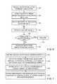
- FIG. 7is a flow chart that schematically illustrates a method for redundant data storage using logical address redundancy, in accordance with another embodiment of the present invention.
- FIG. 8is a flow chart that schematically illustrates a method for redundant data readout, in accordance with an embodiment of the present invention.
- Embodiments of the present inventionthat are described hereinbelow provide improved methods and systems for redundant data storage in solid-sate non-volatile memory, such as Flash memory.
- the disclosed techniquesmay be carried out, for example, by a memory controller that stores data in multiple memory units, such as individual memory dies or packaged memory devices.
- the methods described hereinenable the memory controller to recover the stored data in the event of memory unit failure.
- these methodsinvolve accepting data for storage from a host, computing redundancy information for the data, and storing the data and the redundancy information in different memory units.
- Data storage in solid-state non-volatile memorye.g., Flash memory
- the memory controllerstores data efficiently in spite of the above-described characteristics by using logical addressing.
- the hostaddresses the data for storage using logical addresses.
- the memory controllermaps the logical addresses to respective physical storage locations for storing the data.
- the memory controllerstores the updated data in a new physical storage location, updates the logical-physical address mapping to remap the logical address to the new physical storage location, and marks the previous physical storage location as invalid.
- the blocksgradually develop regions of invalid data (“holes”).
- the memory controllertypically carries out a “garbage collection” process, which copies valid data from partially-valid blocks and stores the data compactly in other blocks. The cleared blocks are subsequently erased in preparation for storing new data.
- the unique characteristics of solid-state non-volatile memorymay have a particularly adverse effect on the performance of redundant storage schemes that are known in the art.
- the redundancy informationis typically updated whenever the data is updated, thus causing a considerable increase in the number of programming operations. This increase may be tolerable in some storage media types, but not in non-volatile solid-state devices that degrade after a limited number of programming cycles.
- the disclosed redundant storage schemesprovide protection against memory unit failure while minimizing the effects of redundant storage on the lifetime and performance of the system.
- the memory controllerperforms redundant storage based on the physical storage locations assigned to the data.
- the memory controllerdefines sets of memory blocks that are referred to as superblocks.
- Each superblockcomprises N blocks, each selected from a different memory unit.
- Each set of N corresponding pages (with one page from each block) in a given superblockis referred to as a super-page.
- Data storageis carried out such that the N pages belonging to a given super-page are programmed together, and the N blocks belonging to a given superblock are erased together. Compaction of the memory is also performed in superblocks.
- the term “together” in this contextmeans that no intervening programming operations are permitted to the super-page during programming of the N pages, and no intervening programming operations are permitted to the superblock during compaction or erasure of the N blocks.
- the memory controllerstores data in a given N-page super-page by accumulating N ⁇ K data pages (1 ⁇ K ⁇ N) in a buffer, computing K pages of redundancy information for the N ⁇ K data pages, and storing the N ⁇ K data pages and K pages of redundancy information together in the N pages of the super-page.
- the redundancy informationis updated only once per N ⁇ K data pages and not per each incoming data page.
- the memory controllerperforms garbage collection by compacting and erasing entire superblocks rather than individual blocks, so as to provide empty superblocks for subsequent redundant data storage.
- the memory controllerperforms redundant storage based on the logical addresses assigned to the data.
- the memory controllerselects N logical addresses, which are mapped respectively to N physical storage locations that reside in N different memory units. When data is accepted for storage from the host, the memory controller uses N ⁇ K of these addresses for storing data, and the remaining K pages for storing redundancy information.
- the logical addresses that are used for storing the redundancy informationundergo a higher number of programming operations, relative to the logical addresses that are used for storing the data. Therefore, in some embodiments, the memory controller stores the redundancy information at a lower storage density than the storage density used for storing the data. The lower storage density increases the endurance of the redundancy information to severe cycling.
- the memory controllerdefines and applies the mapping between logical addresses and physical storage locations, but the redundancy scheme is defined and managed by the host.
- the memory controllerprovides information regarding the logical-physical address mapping to the host, and the host uses this information to define the redundancy scheme.
- the hostdefines the logical addresses such that the data and the redundancy information will be stored in different memory units.
- the memory controlleruses invalid data, which remains in obsolete blocks that were cleared by the garbage collection process, as temporary backup.
- the garbage collection processis defined such that valid data is read from a source block in one memory unit, and then written to a destination block in a different memory unit. If the memory unit holding the destination block fails, and the memory unit holding the (obsolete) source block was not erased yet, the memory controller recovers the data in question from the source block. In some embodiments, the memory controller delays erasure of obsolete source blocks as much as possible, in order to increase the availability of such temporary backup.
- the memory controllerprotects the stored data against memory unit failure by encoding the data with an Error Correction Code (ECC), and distributes the bits of each ECC code word over multiple memory units.
- ECCError Correction Code
- the ECC and the number of memory unitsare selected such that the code word is still decodable when all the bits stored in a given memory unit are lost.
- the bits that are stored in a failed memory unitare identified to the ECC decoder as erasures.
- the memory controllerstores data in N memory units, and redundancy information for the data in an N+1 th memory unit.
- the memory controllerissues a respective read command to each of the N+1 memory units.
- responses for the first N read commands(which may comprise data and/or redundancy information) arrive, the memory controller reconstructs the data from the N responses without waiting for the N+1 th response.
- data readoutis not sensitive to temporarily slow response times, e.g., to delays caused by memory units that are busy with other tasks.
- FIG. 1is a block diagram that schematically illustrates a multi-device memory system 20 , in accordance with an embodiment of the present invention.
- System 20accepts data for storage from a host 24 and stores it in memory, and retrieves data from memory and provides it to the host.
- systemcomprises a Solid-State Disk (SSD) that stores data for a host computer.
- SSDSolid-State Disk
- system 20may be used in any other suitable application and with any other suitable host, such as in computing devices, cellular phones or other communication terminals, removable memory modules such as Disk-On-Key (DOK) devices, Secure Digital (SD) cards, Multi-Media Cards (MMC) and embedded MMC (eMMC), digital cameras, music and other media players and/or any other system or device in which data is stored and retrieved.
- DOKDisk-On-Key
- SDSecure Digital
- MMCMulti-Media Cards
- eMMCembedded MMC
- System 20comprises multiple non-volatile memory devices 28 , each comprising multiple analog memory cells 32 .
- devices 28comprise NAND Flash devices, although various other suitable solid state memory types, such as NOR and Charge Trap Flash (CTF) Flash cells, phase change RAM (PRAM, also referred to as Phase Change Memory—PCM), Nitride Read Only Memory (NROM), Ferroelectric RAM (FRAM), magnetic RAM (MRAM) and/or Dynamic RAM (DRAM) cells, can also be used.
- NAND Flash devicessuch as NOR and Charge Trap Flash (CTF) Flash cells
- PCMPhase Change RAM
- NROMNitride Read Only Memory
- FRAMFerroelectric RAM
- MRAMmagnetic RAM
- DRAMDynamic RAM
- analog memory cellis used to describe any memory cell that holds a continuous, analog value of a physical parameter, such as an electrical voltage or charge. Any suitable type of analog memory cells, such as the types listed above, can be used.
- each memory device 28comprises a non-volatile memory of NAND Flash cells.
- the charge levels stored in the cells and/or the analog voltages or currents written into and read out of the cellsare referred to herein collectively as analog values or storage values.
- the embodiments described hereinmainly address threshold voltages, the methods and systems described herein may be used with any other suitable kind of storage values.
- each memory device 28data is stored in memory cells 32 by programming the cells to assume respective memory states, which are also referred to as programming levels.
- the programming levelsare selected from a finite set of possible levels, and each level corresponds to a certain nominal storage value. For example, a 2 bit/cell MLC can be programmed to assume one of four possible programming levels by writing one of four possible nominal storage values into the cell.
- Memory cells 32are typically arranged in one or more memory arrays (“planes”), each comprising multiple rows and columns. The memory cells in each row are connected to a respective word line, and the memory cells in each column are connected to a respective bit line.
- Each memory arrayis typically divided into multiple pages, i.e., groups of memory cells that are programmed and read simultaneously. Pages are sometimes sub-divided into sectors.
- each pageoccupies an entire row of the array, i.e., an entire word line.
- each word linestores two pages.
- each row (word line)can be divided into two or more pages.
- each rowis divided into two pages, one comprising the odd-order cells and the other comprising the even-order cells.
- a two-bit-per-cell memory devicemay have four pages per row
- a three-bit-per-cell memory devicemay have six pages per row
- a four-bit-per-cell memory devicemay have eight pages per row.
- a given memory devicecomprises multiple erasure blocks (also referred to as memory blocks), i.e., groups of memory cells that are erased together.
- Each memory device 28may comprise a packaged device or an unpackaged semiconductor chip or die. In some embodiments, each memory device 28 comprises multiple dies.
- a typical SSDmay comprise a number of 4 GB devices.
- system 20may comprise any suitable number of memory devices of any desired type and size.
- Each memory device 28comprises an internal NAND controller 36 , which stores data in the memory cells of the device.
- Each NAND controller 36performs data storage and retrieval in its respective memory device in response to NAND commands.
- Each NAND commandtypically specifies writing or reading of a single memory page in the memory device.
- data storage in memory devices 28is carried out by a hierarchical configuration of processors and controllers, which provides a high degree of parallelization of storage tasks, and therefore achieves high storage throughput with small latency.
- Memory devices 28 in system 20are arranged in subsets.
- a Memory Signal Processor (MSP) 40is associated with each subset and performs data storage and retrieval in the subset.
- each MSP 40comprises an Error Correction Code (ECC) unit 44 , which encodes the data for storage with a suitable ECC, and decodes the ECC of data retrieved from memory.
- ECCError Correction Code
- the subsets of memory devices 28(each with its respective MSP) are aggregated into groups that are referred to as channels.
- System 20comprises a main controller 52 , which manages the system operation.
- Main controller 52comprises multiple channel controllers 48 , each responsible for data storage and retrieval in a respective channel.
- the main controlleraccepts commands from host 24 to store and/or retrieve data, and communicates with the MSPs in order to carry out these commands.
- the communication between the main controller and the channel controllers, between the channel controllers and MSPs, and between the MSPs and the NAND controllerscomprise both data and control aspects.
- main controller 52comprises a host interface processor 53 and a main processor 54 .
- the host interface processorforwards host commands between main controller 54 and host 24 , and forwards data between the MSPs and the host.
- Main processor 54executes the host commands, performs Flash management functions on memory devices 28 , and communicates with the MSPs.
- any other suitable main controller configurationcan also be used.
- Flash management functionsmay be partitioned between main processor 54 and MSPs 40 .
- the systemcomprises volatile memory, in the present example one or more Dynamic Random Access Memory (DRAM) devices 56 , connected to main controller 52 .
- DRAMDynamic Random Access Memory
- system 20comprises a total of eight channel controllers 48 and thirty-two MSPs 40 , i.e., each channel controller manages four MSPs.
- each MSPmay manage between one and eight memory devices 28 .
- a given memory device 28may comprise multiple dies.
- any other suitable numbers of channel controllers, MSPs and memory devicescan also be used.
- the number of memory devices managed by each MSPmay differ, for example, according to the storage capacity of system 20 and the storage density of devices 28 .
- the channel controllersmay be omitted.
- the main controllerstores and retrieves data by communicating directly with the MSPs.
- system 20performs logical-to-physical address translation for storing data in memory devices 28 .
- host 24addresses the data using logical addresses.
- Main controller 52maps each logical address to a respective physical storage location in memory devices 28 . The mapping between logical addresses and physical storage locations may change over time, e.g., when data at a certain logical address is updated.
- main controller 52typically maintains a data structure holding the current mapping between logical addresses and physical storage locations. This data structure can be stored, for example, in DRAM 56 or in memory devices 28 .
- NAND controllers 36 , MSPs 40 , channel controllers 48 and main controller 52may be implemented, for example, using software running on suitable Central Processing Units (CPUs), using hardware (e.g., state machines or other logic), or using a combination of software and hardware elements.
- NAND controllers 36 , MSPs 40 , channel controllers 48 and/or main controller 52may comprise general-purpose processors, which are programmed in software to carry out the functions described herein.
- the softwaremay be downloaded to the processors in electronic form, over a network, for example, or it may, alternatively or additionally, be provided and/or stored on non-transitory tangible media, such as magnetic, optical, or electronic memory.
- FIG. 1is an example configuration, which is shown purely for the sake of conceptual clarity. In alternative embodiments, any other suitable memory system configuration can also be used. Elements that are not necessary for understanding the principles of the present invention, such as various interfaces, addressing circuits, timing and sequencing circuits and debugging circuits, have been omitted from the figure for clarity.
- the channel controllersare comprised in the main controller, and the main controller, MSPs and memory devices are implemented as separate Integrated Circuits (ICs).
- memory devices 28 , MSPs 40 , channel controllers 48 and main controller 52may be implemented as separate ICs.
- each subset of devices 28 with its respective MSPcan be fabricated on a common die or device.
- the MSPs, channel controllers and main controllermay be fabricated in a common Multi-Chip Package (MCP) or System-on-Chip (SoC), separate from memory devices 28 and DRAM 56 .
- MCPMulti-Chip Package
- SoCSystem-on-Chip
- the elements of system 20can be partitioned into packaged ICs or semiconductor dies in any other suitable way.
- main controller 52can be implemented in software and carried out by a processor or other element of the host system.
- host 24 and main controller 52may be fabricated on the same die, or on separate dies in the same device package.
- the main controller, channel controllers, MSPs and NAND controllersare collectively regarded herein as a memory controller, which carries out the methods described herein.
- system 20stores data in devices 28 using a redundant configuration, which provides protection against hardware failures.
- system 20stores certain data by computing redundancy information for the data, distributing the data over N ⁇ 1 storage locations, and storing the redundancy information in an N th storage location (N ⁇ 2).
- the N storage locationsare typically selected to reside in different memory units, e.g., different dies, memory devices or channels. When using this sort of redundancy, the data can be recovered using the redundancy information even in the event of memory unit failure.
- redundancy informationis used herein to describe any information that enables recovering the data in the event that parts of the data are lost or corrupted.
- the redundancy informationcomprises a bit-wise exclusive-OR (XOR) of the N ⁇ 1 data portions.
- the datais encoded with an Error Correction Code (ECC) that produces redundancy bits, the data is stored in N ⁇ 1 locations, and the redundancy bits are stored in the N th location.
- ECCError Correction Code
- system 20may store the data in N ⁇ K locations, 1 ⁇ K ⁇ N, and store the redundancy information in K locations.
- each memory unitmay comprise a memory plane or even a word line, group of word lines or memory block.
- a configuration that spreads the data and redundancy across multiple memory unitsprovides protection against failure of that type of memory unit.
- the basic memory unitis a die
- the disclosed techniquesprovide protection against die failure.
- the basic memory unitis a SSD channel
- the disclosed techniquesprovide protection against channel failure.
- Data storage in non-volatile memoryhas certain unique characteristics. In particular: (1) data is stored page by page, (2) stored data cannot be updated in-place and therefore the updated data needs to be stored in another physical location, (3) data is erased block by block, each block containing multiple pages, and (4) non-volatile memory is specified to endure only a limited number of programming and erasure cycles. When implementing redundant storage schemes, these characteristics may have major impact on system performance.
- Embodiments of the present inventionprovide improved methods and systems for redundant storage in non-volatile memory. These techniques provide protection against memory unit failure, while minimizing the effects of redundant storage on the lifetime and performance of the system.
- the disclosed techniquesmay be carried out by main processor 54 , channel controllers 48 , MSPs 40 , NAND controllers 36 , or any suitable combination or subset of these processors.
- the processor or processors that carry out the disclosed techniques in a given configurationis sometimes referred to as “processing circuitry.”
- the disclosed techniquescan be partitioned among the different processors in any suitable way.
- system 20defines superblocks by associating memory blocks from different dies.
- Each superblockcomprises N blocks, each block selected from a different die.
- each set of N corresponding pages in the N blocks of a given superblockis referred to as a super-page. All the blocks in a given superblock are compacted and erased together, and all the pages in a given super-page are programmed together.
- FIG. 2is a diagram that schematically illustrates a memory superblock, in accordance with an embodiment of the present invention.
- the example of FIG. 2shows N memory dies denoted # 1 . . . #N, each die comprising multiple memory blocks 58 .
- the figureshows a superblock 56 , which comprises N blocks 62 A . . . 62 N. Each block in the superblock resides in a different die. As will be explained below, all the blocks in the superblock are erased together when system 20 compacts the data that is stored in memory.
- Each memory block 58comprises multiple pages 66 .
- system 20regards each set of corresponding pages in the superblock (i.e., N pages, one from each block of the superblock) as a super-page.
- the pages of a given super-pageare programmed together.
- the blocks of a given superblockare not necessarily located in the same location in their respective dies.
- the pages of a given super-pageare not necessarily located in the same location in their respective blocks.
- system 20When using super-pages, system 20 accumulates N ⁇ 1 pages of incoming data (e.g., in a volatile memory buffer) and then calculates the redundancy information for the N ⁇ 1 pages. Then, system 20 stores the data and redundancy information in a single super-page—The data is stored in N ⁇ 1 pages and the redundancy information in the N th page. Therefore, the redundancy information (N th page) is updated only once per N ⁇ 1 pages and not per each incoming page. This technique reduces the additional cycling caused by the redundant storage. If a certain die fails, system 20 can recover a given page stored in that die using (1) the other N ⁇ 2 data pages in the super-page and (2) the redundancy information stored in the N th page of the super-page.
- system 20carries out a “garbage collection” process, which compacts valid data that is stored in the different memory blocks and clears blocks for erasure and new programming.
- Datamay become invalid, for example, when updated data for a certain logical address arrives, and is stored by the system in another physical location. The old data for this logical address is invalid, but cannot be erased immediately because the block may contain other data that is still valid.
- regions of invalid dataaccumulate in the memory blocks.
- the garbage collection processcompacts the data and attempts to minimize the invalid data regions.
- valid datarefers to the most recent copy of the data corresponding to a given logical address, or to the data that is pointed to by the system. Thus, data typically becomes invalid when a more recent copy of the data is stored and pointed to by the system.
- invalid datameans a previous copy of certain data, which is no longer pointed to by the system.
- the garbage collection processmay consolidate valid data from two or more blocks into one or more new blocks.
- the garbage collection processmay copy data from a partially-valid block (i.e., a block having some valid and some invalid pages) into a new block.
- a process of this sortmay be carried out when new data arrives, or as a background process.
- the garbage collection processcopies valid data from one or more partially-valid blocks to other blocks, and then erases the partially-valid blocks that are now obsolete. The erased blocks are available for new programming.
- system 20carries out the compaction and garbage collection process at a superblock level.
- system 20erases all the blocks of a given superblock together. If the total number of blocks is sufficiently large, the number of actual write operations per user write (“write efficiency”) does not change significantly when garbage collection is done by blocks or by superblocks, because the percentage of valid data in each block (or superblock) that is merged during the garbage collection process is approximately the same.
- write efficiencythe number of actual write operations per user write
- the advantage of performing garbage collection at the superblock levelstems from the number of write operations that are needed for storing the redundancy information.
- redundancy blockis stored per N ⁇ 1 data blocks. If garbage collection is carried out at the individual block level, then for the case of random data programming (i.e., the host sends programming commands to random logical addresses), whenever a block is changed, the appropriate redundancy block should also be changed, by issuing another block programming command to the same logical address of the former redundancy block (in a different memory device). Therefore, the number of block write operations for the case of random programming is doubled due to the need to update the redundancy.
- the term “erased together”means that erasure of the memory blocks in a given superblock is performed without allowing any intervening programming operations on the superblock.
- the blocks in a superblockcan be erased in parallel, semi-parallel or even sequentially, as long as no other programming operations are performed in the superblock until all the blocks are erased. Intervening readout operations may be allowed.
- FIG. 3is a flow chart that schematically illustrates a method for redundant data storage using superblocks, in accordance with an embodiment of the present invention. The method begins with system 20 defining superblocks, and super-pages within the superblock, at a superblock definition step 70 .
- system 20After defining the superblock, system 20 carries out two processes irrespective of one another, namely a data storage process and a garbage collection process.
- system 20accumulates N ⁇ 1 pages of data that is accepted for storage from host 24 , at a data accumulation step 72 .
- the systemcomputes redundancy information for the accumulated data, at a redundancy computation step 76 .
- the systemmay calculate the bit-wise XOR of the N ⁇ 1 data pages, to produce an N th redundancy page.
- the systemthen stores the N pages (N ⁇ 1 data pages and redundancy page) in the N pages of a given super-page, at a storage step 80 .
- each of the N pagesis stored on a different die.
- the datacan be recovered using the redundancy information in the event of die failure.
- system 20selects one or more partially-valid superblocks (superblocks whose blocks contain some valid and some invalid pages) for data consolidation (also referred to as compaction), at a superblock selection step 84 .
- System 20may select superblocks for compaction using any suitable criterion. Typically, the criterion depends on the distribution of invalid data in the superblocks. For example, the system may select to compact the superblocks having the largest number of invalid pages. The system then consolidates the valid data from the selected superblocks, at a data consolidation step 88 .
- the compaction processmay copy the valid data from two or more selected superblocks to a new superblock, copy the valid data from one partially-valid superblock into another partially-valid superblock, or copy the valid data from a single selected superblock to a new superblock, for example.
- step 88produces at least one obsolete superblock, whose valid data was copied to another superblock.
- System 20erases the obsolete superblock, at a superblock erasure step 92 . As noted above, all the blocks in the superblock are erased without allowing any intervening programming operations in the superblock.
- system 20may copy valid data from a source superblock to a destination superblock using intra-die and/or inter-die copy operations.
- the systemallows valid data to be copied from a source block in one die to a destination block in a different die. For example, the system may read the valid data from the entire source superblock, and write it sequentially to the destination superblock. Allowing inter-die copy operations enables a high degree of flexibility, and potentially achieves tighter compaction. Inter-die copy operations may be particularly advantageous when the invalid pages (“holes”) are not distributed uniformly across the blocks of the source superblock. On the other hand, inter-die copy operations cause considerable data traffic to pass through MSPs 40 , channel controllers 48 and/or main processor 54 .
- system 20performs superblock compaction using only intra-die copy operations.
- copy operationscan be performed by NAND controllers 36 internally in memory devices 28 , without transferring data through the MSPs, channel controllers and main processor. Partial limitations are also possible.
- inter-die copy operationsmay be permitted only between dies in the same memory device, between dies that are managed by the same MSP, or between dies that are managed by the same channel controller.
- system 20may select an additional source superblock (e.g., the superblock having the next-highest number of invalid pages), and copy valid data from this superblock to the destination superblock.
- the systemmarks the copied pages as invalid in the new source superblock. If necessary, this process can be repeated (by progressively adding additional source superblocks) until the destination superblock is full.
- FIG. 4is a diagram that schematically illustrates a process of superblock compaction, in accordance with an embodiment of the present invention.
- a first source superblock 94is compacted into a destination superblock 94 C.
- the valid super-pages in superblock 94 Aare fragmented, and the memory controller thus copies them in a compact manner to superblock 94 C.
- the memory controllerselects superblock 94 B as the next superblock for compaction. Since destination superblock 94 C still has super-pages that are available for programming, the memory controller copies the valid super-pages from source superblock 94 B to destination superblock 94 C. This process may continue as long as the destination superblock is not full.
- the number of invalid pages (“holes”)may vary considerably from die to die. For example, some dies may hold static data that is rarely updated, and therefore have few invalid pages. Other dies may hold data that is updated frequently, and therefore have a large number of invalid pages. In system configurations that allow only intra-die copy, the compaction of superblocks may be degraded considerably. In some embodiments, system 20 avoids unbalanced scenarios of this sort by running a background process that copies blocks from die to die.
- system 20classifies the data for storage to rarely-updated (“static” or “cold”) data and frequently-updated (“dynamic” or “hot”) data. Using the classification, the system stores the rarely-updated data and frequently-updated data in separate superblocks. This sort of separation increases the compaction efficiency. In contrast, if rarely-updated and frequently-updated data were to be stored in the same superblock, the system may have to copy rarely-updated data to another superblock unnecessarily, in order to be able to erase the superblock, even though the rarely-updated data has few “holes.”
- systemassesses the update frequency of the data (e.g., by recording the most recent time at which each logical address was programmed). Using this assessment, the system can assign rarely-updated data and frequently-updated data to separate superblocks.
- system 20redefines the superblock to have a smaller number of blocks. The failed block is thus removed from the redefined superblock.
- each superblockcomprises N blocks having corresponding physical addresses in N different memory units (dies in the present example).
- the N blocks in each superblockcomprise N ⁇ 1 data blocks and a redundancy block.
- the systemredefines the superblock to include only the remaining N ⁇ 1 blocks, e.g., N ⁇ 2 data blocks and a redundancy block. If another block in the superblock fails, the process may continue by redefining the superblock to include a total of N ⁇ 2 blocks.
- This techniqueavoids the need to redefine the entire assignment of blocks to superblocks in the system in the event of block failure. In other words, the effect of a failed block is confined to the superblock containing that failed block.
- the description aboverefers to a scheme in which each superblock comprises blocks having corresponding physical addresses in multiple dies, the disclosed technique is not limited to this assignment and can be used in superblocks having any other suitable block selection.
- the systemstores data in K blocks of a given superblock and redundancy information in the remaining N ⁇ K pages of the given superblock.
- the data and redundancy information in a given superblockmay be interleaved over the N blocks, such that at least one of the blocks (and often all N blocks) in the superblock comprises both data and redundancy information.
- system 20receives from host 24 data that is addressed using logical addresses, and stores the data in respective physical storage locations in memory devices 28 .
- the translation between logical addresses and physical storage locationsis performed in accordance with a logical-physical address mapping that is defined and updated by main controller 52 .
- the redundancy schemeis defined and carried out entirely within system 20 .
- the hosthas no knowledge or involvement in the redundant storage process, and may not even be aware that redundancy information is produced and stored.
- the following descriptionpresents embodiments in which the redundancy scheme is applied by the host, based on information regarding the logical-to-physical address mapping that is provided by system 20 .
- main controller 52provides to host 24 information regarding the logical-physical address mapping.
- the information provided by controller 52indicates which logical addresses are mapped to each die.
- controller 52may send to host 24 a set of logical address ranges, each range comprising the logical addresses mapped to a respective die.
- the hostcan cause a particular data item to be stored in a particular die, by assigning this data item a logical address that is mapped to the desired die.
- the information reported by controller 52enables the host to control the physical storage locations in which system 20 will store data, even though system 20 applies logical-to-physical address translation. This mechanism enables the host to implement various redundancy schemes in system 20 , by assigning appropriate logical addresses to the data.
- the hostmay generate redundancy information for certain data, and assign the data and the redundancy information logical addresses that cause them to be stored in different dies.
- the hostaccumulates N ⁇ 1 data pages, and calculates a redundancy page over the data using bit-wise XOR. Then, the host assigns the N ⁇ 1 data pages and the N th redundancy page N logical addresses, which cause the N pages to be stored in N different dies.
- the hostis able to assign the logical addresses appropriately, based on the information regarding the logical-physical mapping that is reported by controller 52 .
- the hostcan use information regarding the logical-physical mapping to implement any suitable redundant storage scheme, such as various RAID schemes.
- system 20typically updates the host with these changes. The updates can be reported as they occur, or on a periodic basis.
- system 20 and host 24support an interface, over which controller 52 reports the information regarding the logical-physical address mapping to the host.
- FIG. 5is a flow chart that schematically illustrates a method for redundant data storage, in accordance with another embodiment of the present invention.
- the methodbegins with main controller 52 in system 20 defining a mapping between logical addresses and physical storage locations, at a mapping definition step 100 .
- Controller 52reports information regarding the mapping to host 24 , at a mapping reporting step 104 .
- controller 52indicates to host 24 which logical addresses are mapped to each die.
- host 24When preparing to store data in system 20 , host 24 assigns logical addresses to the data based on the reported information regarding the mapping, at an address assignment step 108 . Typically, the host produces redundancy information for the data. Then, the host assigns the data and the redundancy information logical addresses, which will cause system 20 to store them in different dies.
- the hostmay implement any suitable redundancy scheme in system 20 using this technique, such as various RAID schemes.
- Host 24sends the data and redundancy information to controller 52 in system 20 for storage, at a sending step 112 .
- Each data item(including data and redundancy information) is sent with the respective logical address that was assigned at step 108 above.
- System 20stores the data and redundancy information in memory devices 28 , at a storage step 116 .
- system 20translates the logical addresses to respective physical storage locations according to the mapping, and stores the data items at these physical storage locations. Since the logical addresses were assigned by the host based on the reported mapping, each data item will be stored in a different die. If a certain die fails, host 24 can recover the data item stored on that die based on (1) the data items that is stored on the remaining dies and (2) the redundancy information.
- system 20carries out a garbage collection process, which copies valid data from partially-valid blocks (“source blocks”) and stores the data in a compact manner in other blocks (“destination blocks”). Once all valid data is copied from a given source block, the source block is regarded as obsolete and may be erased.
- garbage collection processwhich copies valid data from partially-valid blocks (“source blocks”) and stores the data in a compact manner in other blocks (“destination blocks”). Once all valid data is copied from a given source block, the source block is regarded as obsolete and may be erased.
- system 20uses the obsolete data that is stored in obsolete source blocks as temporary backup, and recovers the data from the obsolete blocks in the event of failure in the destination blocks.
- system 20implements this temporary backup scheme by (1) specifying that the source and destination blocks of any given data item will reside in different dies, and (2) delaying erasure of obsolete blocks as much as possible. These two guidelines increase the likelihood that, when a given die fails, the data of this die can still be recovered from obsolete blocks that formerly held the data.
- FIG. 6is a flow chart that schematically illustrates a method for garbage collection and recovery from die failure, in accordance with another embodiment of the present invention.
- the methodbegins with system 20 selecting a source block for garbage collection, at a source selection step 120 .
- the selected source blockresides in a certain die, denoted die X.
- System 20selects a destination block for copying the valid data from the source block, at a destination selection step 124 .
- System 20selects the destination block in a die denoted Y, which is different from die X.
- System 20copies the valid data from the source block in die X to the destination block in die Y.
- System 20marks the source block as obsolete, i.e., ready for erasure.
- system 20delays the actual erasure of the source block, at a delaying step 128 .
- the delay in erasureextends the time period in which the data in the source block, although marked as invalid, is still available for readout if necessary.
- System 20can delay erasure of the source block in various ways. For example, system 20 may hold the obsolete blocks without erasing them, until a new block is needed for programming. As another example, the system may hold a relatively small pool of blocks that are erased and ready for programming, and delay erasure of the remaining obsolete blocks.
- system 20identifies a failure in die Y (the die comprising the destination block), at a failure detection step 132 .
- System 20checks whether an obsolete replica of the data of die Y is still available for recovery.
- system 20checks whether the obsolete source block in die X (from which the data was copied to the destination block) has been erased, at an erasure checking step 136 . If the obsolete source block was erased, the method terminates without recovering the data, at a failure termination step 140 . If, on the other hand, the obsolete source block in die X was not erased yet, system 20 recovers the data in question by reading it from the source block, at a recovery step 144 .
- the scheme of FIG. 6does not provide guaranteed backup, since the data is available for recovery only until the obsolete block is erased. On the other hand, this scheme provides some degree of backup without requiring additional memory or other system resources.
- the source and destination blocksare selected in different dies. In alternative embodiments, however, the source and destination blocks may be selected in the same die, and the disclosed technique can be used for recovery from failure in the source block.
- system 20implements a redundancy storage scheme based on the logical addresses (sometimes referred to as Logical Block Addresses—LBAs) that are assigned to the data by the host.
- main controller 52 in system 20assigns a dedicated LBA for each group of N ⁇ 1 LBAs assigned by the host.
- the dedicated LBAalso referred to as “redundancy LBA”
- the dedicated LBAis used for storing redundancy information that is computed over the data of the N ⁇ 1 LBAs in the group (also referred to as “host LBAs”).
- Controller 52typically assigns the redundancy LBAs in a range of LBAs that is not accessible to host 24 .
- system 20ensures that each of the N LBAs in the group (the N ⁇ 1 host LBAs and the redundancy LBAs) is stored in a different die. For example, when defining the logical-physical address mapping, controller 52 may assign each die a certain respective range of LBAs, which does not overlap the ranges assigned to the other dies. Then, when selecting a group of N ⁇ 1 LBAs for redundant storage, controller 52 selects each LBA from the range of a different die. Alternatively, controller 52 may ensure or verify that each LBA in the group maps to a different die using any other suitable method.
- controller 52attempts to avoid situations in which the redundancy LBAs are assigned in the same die or in a small group of dies. A situation of this sort would cause severe cycling and wear of the die or dies holding the redundancy LBAs. Thus, in some embodiments, controller 52 attempts to distribute the redundancy LBAs of different LBA groups across multiple dies. For sequential programming, the updating overhead is smaller. Therefore, this technique is particularly useful in applications that are dominated by random write operations, e.g., in transaction servers. Nevertheless, the technique is useful for sequential storage applications, as well.
- system 20may store the redundancy LBAs using a storage configuration that is more resilient to severe cycling, in comparison with the storage configuration used for storing the host LBAs.
- system 20may partition each die into two subsets of memory cells.
- One subsetreferred to as a high-endurance area, stores data at a lower density (lower number of bits/cell, smaller number of programming levels), but on the other hand at a higher endurance.
- the other subsetreferred to as a high-density area, stores data at a higher density, but at a lower resilience to cycling.
- System 20stores the host LBAs in the high-density area, and the redundancy LBAs in the high-endurance area.
- the memory cells in this areacan tolerate considerably more endurance, i.e., higher numbers of programming and erasure cycles, relative to the memory cells in the high-density area. As such, it is preferable to store the redundancy LBAs in the high-endurance area. This technique, however, causes some degradation in capacity due to the lower storage density in the high-endurance area.
- System 20can define the high-endurance and high-density storage configurations in any desired manner.
- the systemmay store the host LBAs in the high-density area using N programming levels (programming states) per cell, and store the redundancy LBAs in the high-endurance area using M programming levels, M ⁇ N.
- system 20stores the host LBAs using a Multi-Level Cell (MLC) configuration having four levels or eight levels, and the redundancy LBAs using a Single-Level Cell (SLC) configuration having two programming levels.
- MLCMulti-Level Cell
- SLCSingle-Level Cell
- the host LBAsmay be stored using three programming levels, and the redundancy LBAs using two bits/cell (SLC).
- any other suitable values of N and Mcan be used.
- FIG. 7is a flow chart that schematically illustrates a method for redundant data storage using logical address redundancy, in accordance with another embodiment of the present invention.
- the methodbegins with main controller 52 defining a mapping between logical addresses (LBAs) and physical storage locations, at a mapping specification step 150 .
- Controller 52selects N LBAs that are mapped to N respective physical storage locations in N different dies, at a group selection step 154 .
- One of the N LBAs(the redundancy LBA) is selected from a range of LBAs that is not accessible to the host, and is designated for storing redundancy information.
- the other N ⁇ 1are referred to as host LBAs.
- the group of N LBAsis referred to as a logical stripe.
- Controller 52stores incoming data from the host in the host LBAs, and redundancy information in the redundancy LBA.
- redundancy informationFor example, new data that arrives from the host and is addressed to one of the host LBAs in the group.
- controller 52updates the redundancy information for this group to reflect the new data.
- Controller 52then stores the data in the host LBA, at a first storage step 158 , and the updated redundancy information in the redundancy LBA, at a second storage step 162 .
- controller 52stores the host LBA at high density (e.g., in a high-density area assigned in the respective die), and the redundancy LBA at a high-endurance configuration (e.g., in a high-endurance area assigned in the respective die).
- FIG. 7refers to a single logical stripe, i.e., a single group of N LBAs. Generally, however, system 20 defines multiple logical stripes. In an example embodiment, the entire range of LBAs is divided into logical stripes, i.e., groups of N LBAs. Data storage within each logical stripe is carried out using the method of FIG. 7 .
- system 20protects the stored data from die failures by encoding the data with an ECC, and distributing the bits of each ECC code word over multiple dies.
- ECCError Correction Code
- system 20encodes incoming data, to produce ECC code words.
- Each code wordcomprises multiple bits, e.g., several hundred or several thousand bits.
- System 20distributes (interleaves) the bits of each code word across the thirty-three dies. If any single die fails, approximately 3% of the bits in each code word will be lost. For a properly chosen ECC, the entire data can be recovered from the code words in the absence of the 3% lost bits.
- the lost bitscan be pointed out to the ECC decoder as erasures, since the identity of the failed die is often known.
- ECC typessuch as Reed-Solomon (RS) or Low-Density Parity Check (LDPC) codes, have a considerably higher correction capability when provided with erasure information. This technique is useful not only for die failures that cause total data loss, but also for failures that cause high bit error rate on one or more dies.
- the bitsare associated with respective soft metrics (e.g., Log Likelihood Ratios—LLRs), and the ECC decoder decodes the code word using the soft metrics.
- LLRsLog Likelihood Ratios
- system 20may apply any of the redundant storage techniques disclosed herein (e.g., any of the disclosed logical and/or physical addressing schemes, and/or any other disclosed techniques for using spare memory units) in storing the subsets of bits of the ECC code word in the multiple memory units.
- redundant storage techniquese.g., any of the disclosed logical and/or physical addressing schemes, and/or any other disclosed techniques for using spare memory units
- system 20comprises one or more spare dies that are reserved for replacing failed dies.
- a spare dieis not used for storing data until it replaces a failed die.
- the spare diesprovide additional physical storage space, which can be used for storing data at improved performance. In the event of die failure, less physical space is available, but the available physical space still meets the system specification. Any of the redundant storage techniques described herein can be used in conjunction with spare dies.
- N+1 th diecan be added.
- the N+1 this not used as long as the other N dies are functional. If one of the N dies fails, the data stored in the failed die can be recovered based on the redundancy information, and copied to the spare die. From that point, the system can continue to operate with N dies as before.
- the data of the failed diecan be restored to the spare die gradually. For example, whenever certain data is accessed, the data is restored and then programmed to the spare die. Alternatively, the entire content of the failed die can be restored upon detecting that the die has failed.
- DDPDual-Die Packages
- the systeminherently comprises a spare die.
- the spare diesare used during normal operation, and therefore increase the ratio between physical storage space and the logical address range accessible by the host.
- the additional physical storage spacecan be used for various purposes.
- the additional physical spacecan used to increase the Over-Provisioning ratio of system 20 , i.e., the average number of invalid data regions (“holes”) per block.
- Higher over-provisioning overheadincreases the efficiency of the garbage collection process, and therefore improves programming throughput.
- the over-provisioning overheaddecreases due to the lower available physical storage space.
- system 20computes redundancy information for data items that are stored on multiple dies.
- system 20can distribute this computation over multiple processors, such that each processor computes partial redundancy information for the dies it is associated with.
- each processorcomputes partial redundancy information for the dies it is associated with.
- it is assumed that the redundancy calculationcan be partitioned into several independent sub-calculations whose results can be subsequently combined.
- Exclusive OR (XOR) redundancyfor example, meets this condition.
- the redundancy informationcan be computed in a centralized manner by main controller 52 .
- each MSP 40can calculate partial redundancy information over the dies it is responsible for. Then, main controller 52 can combine the multiple partial redundancy information in order to derive the total redundancy information pertaining to all the dies.
- each MSP 40calculates partial redundancy information over its respective dies, and each channel controller combines the partial redundancy information from its respective MSPs to produce a channel-level result.
- the main controllercombines the channel-level results of the channel controllers to produce the total redundancy information.
- system 20can partition the redundancy computation in any other suitable manner. This technique reduces the computational burden on the main controller and channel controllers, and also increases storage speed.
- the memory controllerstores data in N memory units (e.g., dies), and redundancy information for the data in an N+1 th memory unit.
- the memory controllerissues read commands to the memory units.
- some memory unitsmay be slow in responding to the read commands. For example, a given memory unit may be busy with another task (e.g., erasure, read threshold estimation, programming or readout) and will therefore respond after a relatively long delay.
- the memory controllerreduces the sensitivity of the readout process to delays by reconstructing the data without waiting for the slowest memory unit.
- the memory controllerissues a respective read command to each of the N+1 memory units, including both the N memory units holding the data and the N+1 th memory unit holding the redundancy information.
- the memory controllerreconstructs the data from the N responses without waiting for the N+1 th response.
- the first N memory units to respondare the ones holding the data (i.e., the memory unit holding the redundancy information is the slowest), in which case the memory controller has all the data ready.
- the first N memory units to respondare N ⁇ 1 of the memory units holding the data, and the memory unit holding the redundancy information. In this case, the memory controller reconstructs the data of the remaining memory unit, which has not yet responded, based on the data read from the other N ⁇ 1 memory units and the redundancy information read from the N+1 th memory unit.
- FIG. 8is a flow chart that schematically illustrates a method for redundant data readout, in accordance with an embodiment of the present invention.
- the methodbegins with the memory controller storing N data units (N data pages in the present example) in N respective dies, and a redundancy data unit (a redundancy page in the present example) holding redundancy information for the data in an N+1 th die, at a redundant storage step 170 .
- the memory controllermay use any suitable redundancy scheme, such as any of the schemes described above.
- the memory controlleris requested to retrieve the store data.
- the memory controllerissues N+1 read commands to the N+1 dies in question, at a read instruction step 174 .
- the memory controllerwaits until the first (fastest) N pages arrive, at an arrival checking step 178 .
- the memory controllerreconstructs the data based on these N pages, at a data reconstruction step 182 , irrespective of the N+1 th page. If the first N pages are the data pages, the data is already available. If the first N pages are N ⁇ 1 data pages and the redundancy page, the memory controller reconstructs the data of the N+1 th page based on the N data pages and the redundancy page.
- the memory controllerthen outputs the reconstructed data.
- a dieor other memory unit that is slow to respond to readout commands does not delay the entire readout process.
- system 20supports an interface using which the memory units report their expected response latencies to the memory controller.
- the memory controllerqueries each memory unit before retrieving the data, and in return each memory unit reports its expected response latency.
- the memory controllerselects the N memory units having the lowest expected latencies (from among the N+1 memory units in question), and issues read commands only to the N selected memory units. If two or more memory units report the same expected latency, the memory controller may choose between them according to another criterion, e.g., the memory units having the smallest number of pending read requests. Alternatively, any other suitable criterion can be used.
- the slow response time of a given diemay be caused by various background tasks (e.g., garbage collection and/or housekeeping tasks) that are performed by the memory controller on the memory units.
- the memory controllerschedules background tasks in the different memory units (e.g., dies), so as to enable fast readout. For example, the memory controller may schedule background tasks in the N+1 memory units using “round robin” scheduling, such that at any given time there are N memory units that are not busy executing background tasks.
- the N+1 th memory unitwas slow to respond because the read thresholds that were used for reading the memory cells were not positioned properly.
- the memory controllerafter successfully reconstructing the data based on the other N readout results, the memory controller provides the reconstructed data of the N+1 th memory unit to the N+1 th memory unit. This data can be used by the N+1 th memory unit, for example, to find the correct locations of the read thresholds.
- the reconstructed data provided to the N+1 th memory unit by the memory controllercan be used by the N+1 th memory unit to improve, speed-up or generally enable subsequent readout in any other suitable way.
- the memory controllerstores data in N memory units and redundancy information in an N+1 th memory unit, and recovers the data using the N memory units that are fastest to respond to read requests.
- the memory controllermay store data in a total of N+K memory units, such that N memory units hold data and the remaining K memory units hold redundancy information. The memory controller then may recover the data using any partial subset of the memory units that are fastest to respond.
- the memory controllerissues read requests to all N+K memory units. In some embodiments, however, the memory controller may issue less than N+K read commands. For example, the memory controller may have information indicating that a given memory unit is busy with another task. In this scenario, the memory controller may a-priori refrain from issuing a read command to this memory unit, and prefer to recover the data from the remaining memory units.
- the memory controllerapplies a programming scheme that stores incoming data efficiently in RAID stripes, and performs redundancy information updates only during block compaction (“garbage collection”).
- the memory controllerstores data in groups of N logical pages that are referred to as RAID stripes.
- Each RAID stripecomprises a certain amount of incoming user data (e.g., N ⁇ K pages) and a certain amount (e.g., K pages) of redundancy information computed over the user data.
- the memory controllermaintains a database of pointers that point to the physical storage addresses of the N pages in each RAID stripe, which are typically distributed over N memory units.
- the memory controllerarranges the data, with redundancy information, in RAID stripes and stores the RAID stripes in the memory units. Since each all N pages of a given RAID stripe are stored at the same time, there is no need for updating of redundancy information during programming. As a result, the programming process is fast and efficient.
- the memory controllerselects for compaction memory blocks, which contain some invalid pages. Each invalid page belongs to a certain RAID stripe.
- the memory controllerapplies compaction by reading one or more invalid pages, reading the redundancy information of the RAID stripe(s) to which these invalid pages belong, replaces the data of the invalid pages with new data, updates the redundancy information based on the invalid pages and the new data, and writes the new data and the updated redundancy information to new physical storage locations.
- the memory controllerupdates the pointer database with the new physical storage locations of the new data and the updated redundancy information.
- This schemeis advantageous, for example, in applications where programming commands arrives in short bursts.
- the programming throughputis not degraded by redundancy information updates. All redundancy updates are performed during the background compaction process.
- the embodiments described hereinrefer mainly to redundant storage schemes in which resilience to failure is achieved by using memory units that reside on different dies or memory devices.
- the memory units that are referred to in the disclosed schemesmay comprise logical memory units, which do not necessarily reside on different dies or devices.
- a given memory diemay be partitioned into two or more logical memory units, each logical memory unit comprising a respective subset of the address space of that die. Any of the methods and systems described herein can be carried out using such logical memory units.
- Hybrid solutionsin which memory units are distributed on different dies but each die may comprise more than one memory unit, are also possible.
Landscapes
- Engineering & Computer Science (AREA)
- Theoretical Computer Science (AREA)
- Physics & Mathematics (AREA)
- General Engineering & Computer Science (AREA)
- General Physics & Mathematics (AREA)
- Quality & Reliability (AREA)
- Human Computer Interaction (AREA)
- Computer Security & Cryptography (AREA)
- Techniques For Improving Reliability Of Storages (AREA)
Abstract
Description
- Data is typically stored page by page, but erased block by block. Each block comprises multiple pages.
- Stored data cannot be updated in-place, and therefore updated data is typically stored in another physical location.
- The memory is specified to endure only a limited number of programming and erasure cycles.
Claims (42)
Priority Applications (3)
| Application Number | Priority Date | Filing Date | Title |
|---|---|---|---|
| US12/987,174US8572311B1 (en) | 2010-01-11 | 2011-01-10 | Redundant data storage in multi-die memory systems |
| US14/173,271US8954823B2 (en) | 2010-01-11 | 2014-02-05 | Redundant data storage schemes for multi-die memory systems |
| US14/662,360US9400710B2 (en) | 2010-01-11 | 2015-03-19 | Redundant data storage schemes for multi-die memory systems |
Applications Claiming Priority (4)
| Application Number | Priority Date | Filing Date | Title |
|---|---|---|---|
| US29380810P | 2010-01-11 | 2010-01-11 | |
| US36440610P | 2010-07-15 | 2010-07-15 | |
| US37388310P | 2010-08-16 | 2010-08-16 | |
| US12/987,174US8572311B1 (en) | 2010-01-11 | 2011-01-10 | Redundant data storage in multi-die memory systems |
Publications (1)
| Publication Number | Publication Date |
|---|---|
| US8572311B1true US8572311B1 (en) | 2013-10-29 |
Family
ID=49448752
Family Applications (6)
| Application Number | Title | Priority Date | Filing Date |
|---|---|---|---|
| US12/987,174Active2031-12-31US8572311B1 (en) | 2010-01-11 | 2011-01-10 | Redundant data storage in multi-die memory systems |
| US12/987,175Active2032-03-05US8677203B1 (en) | 2010-01-11 | 2011-01-10 | Redundant data storage schemes for multi-die memory systems |
| US14/173,271ActiveUS8954823B2 (en) | 2010-01-11 | 2014-02-05 | Redundant data storage schemes for multi-die memory systems |
| US14/173,245ActiveUS9015559B2 (en) | 2010-01-11 | 2014-02-05 | Redundant data storage schemes for multi-die memory systems |
| US14/662,360ActiveUS9400710B2 (en) | 2010-01-11 | 2015-03-19 | Redundant data storage schemes for multi-die memory systems |
| US15/191,103Active2031-02-12US9983929B2 (en) | 2010-01-11 | 2016-06-23 | Redundant data storage schemes for multi-die memory systems |
Family Applications After (5)
| Application Number | Title | Priority Date | Filing Date |
|---|---|---|---|
| US12/987,175Active2032-03-05US8677203B1 (en) | 2010-01-11 | 2011-01-10 | Redundant data storage schemes for multi-die memory systems |
| US14/173,271ActiveUS8954823B2 (en) | 2010-01-11 | 2014-02-05 | Redundant data storage schemes for multi-die memory systems |
| US14/173,245ActiveUS9015559B2 (en) | 2010-01-11 | 2014-02-05 | Redundant data storage schemes for multi-die memory systems |
| US14/662,360ActiveUS9400710B2 (en) | 2010-01-11 | 2015-03-19 | Redundant data storage schemes for multi-die memory systems |
| US15/191,103Active2031-02-12US9983929B2 (en) | 2010-01-11 | 2016-06-23 | Redundant data storage schemes for multi-die memory systems |
Country Status (1)
| Country | Link |
|---|---|
| US (6) | US8572311B1 (en) |
Cited By (54)
| Publication number | Priority date | Publication date | Assignee | Title |
|---|---|---|---|---|
| US20130021832A1 (en)* | 2011-07-21 | 2013-01-24 | Renesas Electronics Corporation | Semiconductor device |
| US20140136903A1 (en)* | 2012-11-15 | 2014-05-15 | Elwha LLC, a limited liability corporation of the State of Delaware | Redundancy for loss-tolerant data in non-volatile memory |
| US20140189207A1 (en)* | 2012-12-31 | 2014-07-03 | Alan Welsh Sinclair | Method and system for managing background operations in a multi-layer memory |
| US20150026386A1 (en)* | 2013-07-16 | 2015-01-22 | Yogesh B. Wakchaure | Erase Management in Memory Systems |
| US20150085555A1 (en)* | 2012-05-01 | 2015-03-26 | David G. Carpenter | Packaged memory dies that share a chip select line |
| US8996951B2 (en) | 2012-11-15 | 2015-03-31 | Elwha, Llc | Error correction with non-volatile memory on an integrated circuit |
| US9026719B2 (en) | 2012-11-15 | 2015-05-05 | Elwha, Llc | Intelligent monitoring for computation in memory |
| US20150134621A1 (en)* | 2013-11-08 | 2015-05-14 | Samsung Electronics Co., Ltd. | Swat command and api for atomic swap and trim of lbas |
| US20150324262A1 (en)* | 2014-05-06 | 2015-11-12 | International Business Machines Corporation | Using spare capacity in solid state drives |
| CN105260325A (en)* | 2014-07-17 | 2016-01-20 | 广明光电股份有限公司 | The method of solid state hard drive to collect garbage blocks |
| US9262268B2 (en) | 2013-12-20 | 2016-02-16 | Seagate Technology Llc | Method to distribute user data and error correction data over different page types by leveraging error rate variations |
| US20160103622A1 (en)* | 2014-10-13 | 2016-04-14 | Silicon Motion, Inc. | Non-volatile memory devices and controllers |
| US9323499B2 (en) | 2012-11-15 | 2016-04-26 | Elwha Llc | Random number generator functions in memory |
| US9442854B2 (en) | 2012-11-15 | 2016-09-13 | Elwha Llc | Memory circuitry including computational circuitry for performing supplemental functions |
| US9519578B1 (en) | 2013-01-28 | 2016-12-13 | Radian Memory Systems, Inc. | Multi-array operation support and related devices, systems and software |
| US20170004037A1 (en)* | 2015-07-03 | 2017-01-05 | SK Hynix Inc. | Memory device with different parity regions |
| KR20170015757A (en)* | 2015-07-31 | 2017-02-09 | 에스케이하이닉스 주식회사 | Data storage device and operating method thereof |
| US20170038985A1 (en)* | 2013-03-14 | 2017-02-09 | Seagate Technology Llc | Nonvolatile memory data recovery after power failure |
| US9582201B2 (en) | 2014-09-26 | 2017-02-28 | Western Digital Technologies, Inc. | Multi-tier scheme for logical storage management |
| US9582465B2 (en) | 2012-11-15 | 2017-02-28 | Elwha Llc | Flexible processors and flexible memory |
| US9606873B2 (en) | 2014-05-13 | 2017-03-28 | International Business Machines Corporation | Apparatus, system and method for temporary copy policy |
| US20170177225A1 (en)* | 2015-12-21 | 2017-06-22 | Nimble Storage, Inc. | Mid-level controllers for performing flash management on solid state drives |
| US9785572B1 (en)* | 2014-09-09 | 2017-10-10 | Radian Memory Systems, Inc. | Memory controller with multimodal control over memory dies |
| US9817595B2 (en) | 2016-01-28 | 2017-11-14 | Apple Inc. | Management of peak power consumed by multiple memory devices |
| EP3120250A4 (en)* | 2014-03-20 | 2017-12-06 | Hewlett-Packard Enterprise Development LP | Solid state drive operations |
| CN108268212A (en)* | 2016-12-30 | 2018-07-10 | 爱思开海力士有限公司 | Controller and operating method |
| US20180217892A1 (en)* | 2017-01-27 | 2018-08-02 | Western Digital Technologies, Inc. | System and method for implementing super word line zones in a memory device |
| US20180307599A1 (en)* | 2017-04-21 | 2018-10-25 | Fujitsu Limited | Storage system, control device, and method of controlling garbage collection |
| US20190035445A1 (en)* | 2017-07-31 | 2019-01-31 | CNEX Labs, Inc. a Delaware Corporation | Method and Apparatus for Providing Low Latency Solid State Memory Access |
| US20190079836A1 (en)* | 2015-12-21 | 2019-03-14 | Intel Corporation | Predictive memory maintenance |
| US10372368B2 (en)* | 2016-10-13 | 2019-08-06 | International Business Machines Corporation | Operating a RAID array with unequal stripes |
| US10437800B2 (en)* | 2016-12-02 | 2019-10-08 | International Business Machines Corporation | Data migration using a migration data placement tool between storage systems based on data access |
| US10437799B2 (en)* | 2016-12-02 | 2019-10-08 | International Business Machines Corporation | Data migration using a migration data placement tool between storage systems based on data access |
| US20190324670A1 (en)* | 2018-04-23 | 2019-10-24 | SK Hynix Inc. | Storage device and operating method thereof |
| US10649681B2 (en) | 2016-01-25 | 2020-05-12 | Samsung Electronics Co., Ltd. | Dynamic garbage collection P/E policies for redundant storage blocks and distributed software stacks |
| CN111813325A (en)* | 2019-04-12 | 2020-10-23 | 群联电子股份有限公司 | Memory control method, memory storage device, and memory control circuit unit |
| US11036429B2 (en)* | 2019-04-02 | 2021-06-15 | Phison Electronics Corp. | Memory control method, memory storage device and memory control circuit unit to determine a source block using interleaving information |
| US20210200682A1 (en)* | 2019-12-30 | 2021-07-01 | Micron Technology, Inc. | Full multi-plane operation enablement |
| US11079943B2 (en)* | 2018-12-04 | 2021-08-03 | Samsung Electronics Co., Ltd. | Storage devices including improved over provision management and operating methods of such storage devices |
| US11112990B1 (en)* | 2016-04-27 | 2021-09-07 | Pure Storage, Inc. | Managing storage device evacuation |
| US11269769B2 (en)* | 2019-07-24 | 2022-03-08 | SK Hynix Inc. | Memory system and method of operating the same |
| US11315611B2 (en) | 2020-01-07 | 2022-04-26 | SK Hynix Inc. | Processing-in-memory (PIM) system and operating methods of the PIM system |
| US11385837B2 (en)* | 2020-01-07 | 2022-07-12 | SK Hynix Inc. | Memory system |
| CN115080466A (en)* | 2021-03-11 | 2022-09-20 | 西部数据技术公司 | Simplified high-capacity die and block management |
| US11481122B2 (en)* | 2019-12-16 | 2022-10-25 | SK Hynix Inc. | Memory system and operating method thereof |
| US11487474B2 (en)* | 2020-08-14 | 2022-11-01 | SK Hynix Inc. | Memory system and method of operating a memory device included in the same |
| US11513733B2 (en) | 2020-01-07 | 2022-11-29 | SK Hynix Inc. | Processing-in-memory (PIM) system and operating methods of the PIM system |
| US11556416B2 (en) | 2021-05-05 | 2023-01-17 | Apple Inc. | Controlling memory readout reliability and throughput by adjusting distance between read thresholds |
| US11593262B1 (en) | 2018-04-25 | 2023-02-28 | Seagate Technology Llc | Garbage collection command scheduling |
| US11599416B1 (en)* | 2021-09-01 | 2023-03-07 | Micron Technology, Inc. | Memory sub-system using partial superblocks |
| US11693773B2 (en)* | 2019-03-15 | 2023-07-04 | Kioxia Corporation | Systems and methods for implementing a four-dimensional superblock |
| US20230214294A1 (en)* | 2021-12-30 | 2023-07-06 | Micron Technology, Inc. | Host-configurable error protection |
| US11847342B2 (en) | 2021-07-28 | 2023-12-19 | Apple Inc. | Efficient transfer of hard data and confidence levels in reading a nonvolatile memory |
| US11868247B1 (en) | 2013-01-28 | 2024-01-09 | Radian Memory Systems, Inc. | Storage system with multiplane segments and cooperative flash management |
Families Citing this family (60)
| Publication number | Priority date | Publication date | Assignee | Title |
|---|---|---|---|---|
| US9774675B2 (en)* | 2009-08-28 | 2017-09-26 | Entit Software Llc | Automatic redundant logical connections |
| US8572311B1 (en)* | 2010-01-11 | 2013-10-29 | Apple Inc. | Redundant data storage in multi-die memory systems |
| US9183134B2 (en) | 2010-04-22 | 2015-11-10 | Seagate Technology Llc | Data segregation in a storage device |
| US12008266B2 (en) | 2010-09-15 | 2024-06-11 | Pure Storage, Inc. | Efficient read by reconstruction |
| US11614893B2 (en) | 2010-09-15 | 2023-03-28 | Pure Storage, Inc. | Optimizing storage device access based on latency |
| WO2013137851A1 (en)* | 2012-03-12 | 2013-09-19 | Intel Corporation | Distributed codeword portions |
| US8996960B1 (en)* | 2012-06-26 | 2015-03-31 | Inphi Corporation | Vertical error correction code for DRAM memory |
| US9384124B2 (en)* | 2012-07-20 | 2016-07-05 | Kabushiki Kaisha Toshiba | Data storage device, memory control method, and electronic device with data storage device |
| US9448919B1 (en)* | 2012-11-13 | 2016-09-20 | Western Digital Technologies, Inc. | Data storage device accessing garbage collected memory segments |
| US9430376B2 (en)* | 2012-12-26 | 2016-08-30 | Western Digital Technologies, Inc. | Priority-based garbage collection for data storage systems |
| KR101767018B1 (en)* | 2013-09-27 | 2017-08-09 | 인텔 코포레이션 | Error correction in non_volatile memory |
| CN104598386B (en)* | 2013-10-31 | 2018-03-27 | Lsi公司 | By following the trail of and reusing solid-state drive block using two level map index |
| EP2905706B1 (en)* | 2013-12-02 | 2017-04-05 | Huawei Technologies Co., Ltd. | Data processing device and data processing method |
| EP3164796B1 (en) | 2014-07-02 | 2022-02-09 | Hewlett-Packard Development Company, L.P. | Firmware update |
| US10235256B2 (en) | 2014-08-18 | 2019-03-19 | Hitachi Vantara Corporation | Systems and methods for highly-available file storage with fast online recovery |
| KR102210327B1 (en) | 2014-08-21 | 2021-02-01 | 삼성전자주식회사 | Memory device having error inform function |
| KR102161535B1 (en)* | 2014-09-24 | 2020-10-06 | 삼성디스플레이 주식회사 | Display device and method of driving the same |
| US20160147444A1 (en)* | 2014-11-23 | 2016-05-26 | Apple Inc. | Parallel data storage in groups of memory blocks having similar performance characteristics |
| US9619326B2 (en)* | 2014-12-09 | 2017-04-11 | Western Digital Technologies, Inc. | Methods and systems for implementing redundancy in memory controllers |
| CN105701021B (en)* | 2014-12-10 | 2021-03-02 | 慧荣科技股份有限公司 | Data storage device and data writing method thereof |
| US10025669B2 (en) | 2014-12-23 | 2018-07-17 | Nuvoton Technology Corporation | Maintaining data-set coherency in non-volatile memory across power interruptions |
| CN105938419B (en)* | 2015-03-04 | 2019-05-14 | 慧荣科技股份有限公司 | Data storage device and data maintenance method thereof |
| US9645885B2 (en)* | 2015-05-14 | 2017-05-09 | Amplidata Nv | Hybrid distributed storage system |
| US9946461B2 (en)* | 2015-05-15 | 2018-04-17 | ScaleFlux, Inc. | In-flash immutable object processing |
| US10241872B2 (en) | 2015-07-30 | 2019-03-26 | Amplidata N.V. | Hybrid distributed storage system |
| KR102312399B1 (en)* | 2015-09-07 | 2021-10-15 | 에스케이하이닉스 주식회사 | Memory system and operating method thereof |
| US9401226B1 (en) | 2015-09-14 | 2016-07-26 | Qualcomm Incorporated | MRAM initialization devices and methods |
| US10268411B1 (en)* | 2015-11-18 | 2019-04-23 | Veritas Technologies Llc | Policy and heuristic based conversion of write-optimized virtual disk format into read-optimized virtual disk format |
| TWI602186B (en)* | 2015-12-09 | 2017-10-11 | 慧榮科技股份有限公司 | Methods for garbage collection in a flash memory and apparatuses using the same |
| CN106897022B (en)* | 2015-12-17 | 2019-05-31 | 腾讯科技(深圳)有限公司 | A kind of method and device of management storage equipment |
| US10540274B2 (en)* | 2016-03-29 | 2020-01-21 | Micron Technology, Inc. | Memory devices including dynamic superblocks, and related methods and electronic systems |
| KR102573301B1 (en)* | 2016-07-15 | 2023-08-31 | 삼성전자 주식회사 | Memory System performing RAID recovery and Operating Method thereof |
| US11675659B2 (en)* | 2016-07-15 | 2023-06-13 | Advanced Micro Devices, Inc. | DDR memory error recovery |
| US10558398B2 (en)* | 2016-07-29 | 2020-02-11 | Seagate Technology Llc | Reducing read latency |
| US9870478B1 (en)* | 2016-08-03 | 2018-01-16 | International Business Machines Corporation | Data protection for storage device |
| KR102795652B1 (en)* | 2016-08-19 | 2025-04-15 | 에스케이하이닉스 주식회사 | Memory system and operating method for the same |
| KR102547713B1 (en)* | 2016-09-01 | 2023-06-26 | 삼성전자주식회사 | Semiconductor memory device and method of operating the same |
| KR102784728B1 (en) | 2016-11-30 | 2025-03-21 | 삼성전자주식회사 | Memory System |
| KR102747560B1 (en) | 2017-02-10 | 2024-12-31 | 삼성전자주식회사 | Storage device managing duplicated data based on the number of operations |
| US10275307B2 (en) | 2017-03-09 | 2019-04-30 | Hewlett Packard Enterprise Development Lp | Detection of error patterns in memory dies |
| EP3379416B1 (en)* | 2017-03-24 | 2023-06-14 | Nxp B.V. | Memory system |
| CN111966540B (en) | 2017-09-22 | 2024-03-01 | 成都华为技术有限公司 | Storage medium management method and device and readable storage medium |
| KR20190040607A (en)* | 2017-10-11 | 2019-04-19 | 에스케이하이닉스 주식회사 | Memory system and operating method of memory system |
| CN108269606B (en)* | 2018-01-10 | 2020-07-14 | 重庆金山医疗器械有限公司 | Method and system for testing storage parameters of eMMC chip |
| KR102586768B1 (en)* | 2018-03-27 | 2023-10-16 | 에스케이하이닉스 주식회사 | Computing system and operation method thereof |
| KR102483476B1 (en)* | 2018-04-03 | 2023-01-03 | 에스케이하이닉스 주식회사 | Semiconductor memory apparatus supporting repair with data I/O terminal as a unit and method of repairing the semiconductor memory apparatus |
| US10990307B2 (en) | 2018-07-27 | 2021-04-27 | Broadcom International Pte. Ltd. | System and method for providing a configurable storage media interface |
| DE102018121885A1 (en)* | 2018-09-07 | 2020-03-12 | Phoenix Contact Gmbh & Co. Kg | Electronic device for use in an automation system and an automation system |
| US10872039B2 (en)* | 2018-12-03 | 2020-12-22 | Micron Technology, Inc. | Managing redundancy contexts in storage devices using eviction and restoration |
| US10908996B2 (en) | 2019-02-22 | 2021-02-02 | Intel Corporation | Distribution of a codeword across individual storage units to reduce the bit error rate |
| US11062756B2 (en) | 2019-10-14 | 2021-07-13 | Western Digital Technologies, Inc. | Extending operating temperature of storage device |
| US11138071B1 (en)* | 2020-06-22 | 2021-10-05 | Western Digital Technologies, Inc. | On-chip parity buffer management for storage block combining in non-volatile memory |
| US11210168B1 (en)* | 2020-06-25 | 2021-12-28 | Micron Technology, Inc. | Error handling optimization in memory sub-system mapping |
| JP2020198128A (en)* | 2020-08-31 | 2020-12-10 | キオクシア株式会社 | Memory system |
| US11829270B2 (en)* | 2020-10-30 | 2023-11-28 | Seagate Technology Llc | Semiconductor die failure recovery in a data storage device |
| US11630727B2 (en)* | 2021-03-24 | 2023-04-18 | Micron Technology, Inc. | Generating die block mapping after detected failure |
| KR20220147292A (en) | 2021-04-27 | 2022-11-03 | 삼성전자주식회사 | Storage device of performing meta data management and method of operating the same |
| US11947568B1 (en)* | 2021-09-30 | 2024-04-02 | Amazon Technologies, Inc. | Working set ratio estimations of data items in a sliding time window for dynamically allocating computing resources for the data items |
| JP2024039302A (en) | 2022-09-09 | 2024-03-22 | キオクシア株式会社 | Memory system and block management method |
| US12271637B2 (en)* | 2023-08-07 | 2025-04-08 | Dell Products L.P. | Hybrid physical/virtual data addressing with generation indicators |
Citations (525)
| Publication number | Priority date | Publication date | Assignee | Title |
|---|---|---|---|---|
| US3668632A (en) | 1969-02-13 | 1972-06-06 | Ibm | Fast decode character error detection and correction system |
| US3668631A (en) | 1969-02-13 | 1972-06-06 | Ibm | Error detection and correction system with statistically optimized data recovery |
| US4058851A (en) | 1976-10-18 | 1977-11-15 | Sperry Rand Corporation | Conditional bypass of error correction for dual memory access time selection |
| US4394763A (en) | 1979-08-31 | 1983-07-19 | Fujitsu Limited | Error-correcting system |
| US4413339A (en) | 1981-06-24 | 1983-11-01 | Digital Equipment Corporation | Multiple error detecting and correcting system employing Reed-Solomon codes |
| US4556961A (en) | 1981-05-26 | 1985-12-03 | Tokyo Shibaura Denki Kabushiki Kaisha | Semiconductor memory with delay means to reduce peak currents |
| US4558431A (en) | 1982-12-10 | 1985-12-10 | Nec Corporation | Memory system for storing analog information |
| US4608687A (en) | 1983-09-13 | 1986-08-26 | International Business Machines Corporation | Bit steering apparatus and method for correcting errors in stored data, storing the address of the corrected data and using the address to maintain a correct data condition |
| US4654847A (en) | 1984-12-28 | 1987-03-31 | International Business Machines | Apparatus for automatically correcting erroneous data and for storing the corrected data in a common pool alternate memory array |
| US4661929A (en) | 1983-12-23 | 1987-04-28 | Hitachi, Ltd. | Semiconductor memory having multiple level storage structure |
| US4768171A (en) | 1984-06-20 | 1988-08-30 | Nec Corporation | Memory circuit having a plurality of cell arrays |
| US4811285A (en) | 1984-04-02 | 1989-03-07 | The Board Of Trustees Of The Leland Stanford Junior University | Analog storage integrated circuit |
| US4899342A (en) | 1988-02-01 | 1990-02-06 | Thinking Machines Corporation | Method and apparatus for operating multi-unit array of memories |
| US4910706A (en) | 1972-09-11 | 1990-03-20 | Hyatt Gilbert P | Analog memory for storing digital information |
| US4993029A (en) | 1989-03-13 | 1991-02-12 | International Business Machines Corporation | Method and apparatus for randomizing data in a direct access storage device |
| US5056089A (en) | 1988-02-08 | 1991-10-08 | Mitsubishi Denki Kabushiki Kaisha | Memory device |
| US5077722A (en) | 1989-01-06 | 1991-12-31 | Convex Computer Corporation | Disk drive insertion and removal interlock |
| US5126808A (en) | 1989-10-23 | 1992-06-30 | Advanced Micro Devices, Inc. | Flash EEPROM array with paged erase architecture |
| US5163021A (en) | 1989-04-13 | 1992-11-10 | Sundisk Corporation | Multi-state EEprom read and write circuits and techniques |
| US5172338A (en) | 1989-04-13 | 1992-12-15 | Sundisk Corporation | Multi-state EEprom read and write circuits and techniques |
| US5182558A (en) | 1991-10-25 | 1993-01-26 | Halliburton Geophysical Services, Inc. | System for generating correction signals for use in forming low distortion analog signals |
| US5182752A (en) | 1990-06-29 | 1993-01-26 | Digital Equipment Corporation | Method and apparatus for transferring data between a data bus and a data storage device |
| US5191584A (en) | 1991-02-20 | 1993-03-02 | Micropolis Corporation | Mass storage array with efficient parity calculation |
| US5200959A (en) | 1989-10-17 | 1993-04-06 | Sundisk Corporation | Device and method for defect handling in semi-conductor memory |
| US5237535A (en) | 1991-10-09 | 1993-08-17 | Intel Corporation | Method of repairing overerased cells in a flash memory |
| US5272669A (en) | 1991-02-20 | 1993-12-21 | Sundisk Corporation | Method and structure for programming floating gate memory cells |
| US5276649A (en) | 1989-03-16 | 1994-01-04 | Mitsubishi Denki Kabushiki Kaisha | Dynamic-type semiconductor memory device having staggered activation of column groups |
| US5287469A (en) | 1988-12-27 | 1994-02-15 | Nec Corporation | Electrically erasable and programmable non-volatile memory (EEPROM), wherein write pulses can be interrupted by subsequently received read requests |
| US5365484A (en) | 1993-08-23 | 1994-11-15 | Advanced Micro Devices, Inc. | Independent array grounds for flash EEPROM array with paged erase architechture |
| US5388064A (en) | 1991-11-26 | 1995-02-07 | Information Storage Devices, Inc. | Programmable non-volatile analog voltage source devices and methods |
| US5416646A (en) | 1992-11-12 | 1995-05-16 | Kabushiki Kaisha Toshiba | Data recording and reproducing apparatus having read/write circuit with programmable parameter means |
| US5416782A (en) | 1992-10-30 | 1995-05-16 | Intel Corporation | Method and apparatus for improving data failure rate testing for memory arrays |
| US5446854A (en) | 1993-10-20 | 1995-08-29 | Sun Microsystems, Inc. | Virtual memory computer apparatus and address translation mechanism employing hashing scheme and page frame descriptor that support multiple page sizes |
| US5450424A (en) | 1992-07-27 | 1995-09-12 | Mitsubishi Denki Kabushiki Kaisha | Semiconductor memory device with error checking and correcting function |
| US5469444A (en) | 1991-03-12 | 1995-11-21 | Kabushiki Kaisha Toshiba | Electrically erasable and programmable non-volatile memory system with write-verify controller using two reference levels |
| US5473753A (en) | 1992-10-30 | 1995-12-05 | Intel Corporation | Method of managing defects in flash disk memories |
| US5479170A (en) | 1992-10-16 | 1995-12-26 | California Institute Of Technology | Method and apparatus for long-term multi-valued storage in dynamic analog memory |
| WO1996010256A1 (en) | 1994-09-29 | 1996-04-04 | Intel Corporation | Sensing state of a memory by variable gate voltage |
| US5519831A (en) | 1991-06-12 | 1996-05-21 | Intel Corporation | Non-volatile disk cache |
| US5533190A (en) | 1994-12-21 | 1996-07-02 | At&T Global Information Solutions Company | Method for maintaining parity-data consistency in a disk array |
| US5532962A (en) | 1992-05-20 | 1996-07-02 | Sandisk Corporation | Soft errors handling in EEPROM devices |
| US5541886A (en) | 1994-12-27 | 1996-07-30 | Intel Corporation | Method and apparatus for storing control information in multi-bit non-volatile memory arrays |
| US5600677A (en) | 1994-07-08 | 1997-02-04 | Zenith Electronics Corporation | Trellis coded modulation system for digital television signal |
| US5638320A (en) | 1994-11-02 | 1997-06-10 | Invoice Technology, Inc. | High resolution analog storage EPROM and flash EPROM |
| US5657332A (en) | 1992-05-20 | 1997-08-12 | Sandisk Corporation | Soft errors handling in EEPROM devices |
| US5675540A (en) | 1996-01-22 | 1997-10-07 | Micron Quantum Devices, Inc. | Non-volatile memory system having internal data verification test mode |
| US5682352A (en) | 1996-02-08 | 1997-10-28 | Invoice Technology, Inc. | Digital testing of analog memory devices |
| US5687114A (en) | 1995-10-06 | 1997-11-11 | Agate Semiconductor, Inc. | Integrated circuit for storage and retrieval of multiple digital bits per nonvolatile memory cell |
| US5696717A (en) | 1995-10-16 | 1997-12-09 | Samsung Electronics Co., Ltd. | Nonvolatile integrated circuit memory devices having adjustable erase/program threshold voltage verification capability |
| US5726934A (en) | 1996-04-09 | 1998-03-10 | Information Storage Devices, Inc. | Method and apparatus for analog reading values stored in floating gate structures |
| US5726649A (en) | 1994-09-05 | 1998-03-10 | Yamaha Corporation | Control device suitable for use in an apparatus for reproducing video, audio and accompanying characters |
| US5742752A (en) | 1995-12-29 | 1998-04-21 | Symbios Logic Inc. | Method for performing a RAID stripe write operation using a drive XOR command set |
| US5748533A (en) | 1996-03-26 | 1998-05-05 | Invoice Technology, Inc. | Read circuit which uses a coarse-to-fine search when reading the threshold voltage of a memory cell |
| US5748534A (en) | 1996-03-26 | 1998-05-05 | Invox Technology | Feedback loop for reading threshold voltage |
| US5751637A (en) | 1995-06-07 | 1998-05-12 | Macronix International Co., Ltd. | Automatic programming algorithm for page mode flash memory with variable programming pulse height and pulse width |
| US5761402A (en) | 1993-03-08 | 1998-06-02 | Hitachi, Ltd. | Array type disk system updating redundant data asynchronously with data access |
| WO1998028745A1 (en) | 1996-12-20 | 1998-07-02 | Intel Corporation | Nonvolatile writeable memory with fast programming capability |
| US5798966A (en) | 1997-03-31 | 1998-08-25 | Intel Corporation | Flash memory VDS compensation techiques to reduce programming variability |
| US5799200A (en) | 1995-09-28 | 1998-08-25 | Emc Corporation | Power failure responsive apparatus and method having a shadow dram, a flash ROM, an auxiliary battery, and a controller |
| US5801985A (en) | 1995-07-28 | 1998-09-01 | Micron Technology, Inc. | Memory system having programmable control parameters |
| US5838832A (en) | 1995-04-03 | 1998-11-17 | Iterated Systems, Inc. | Method and system for representing a data set with a data transforming function and data mask |
| US5860106A (en) | 1995-07-13 | 1999-01-12 | Intel Corporation | Method and apparatus for dynamically adjusting power/performance characteristics of a memory subsystem |
| US5867428A (en) | 1996-07-09 | 1999-02-02 | Hitachi, Ltd. | Nonvolatile memory system semiconductor memory and writing method |
| US5867429A (en) | 1997-11-19 | 1999-02-02 | Sandisk Corporation | High density non-volatile flash memory without adverse effects of electric field coupling between adjacent floating gates |
| US5867114A (en) | 1996-02-29 | 1999-02-02 | Mitel Corporation | Method and apparatus for performing data compression |
| US5877986A (en) | 1989-04-13 | 1999-03-02 | Sandisk Corporation | Multi-state Flash EEprom system on a card that includes defective cell substitution |
| US5889937A (en) | 1996-06-27 | 1999-03-30 | Nec Corporation | Hard disk apparatus capable of transforming logical addresses of apparatus diagnosis cylinders to HDD-by-HDD physical addresses |
| US5901089A (en) | 1996-04-30 | 1999-05-04 | Agate Semiconductor, Inc. | Stabilization circuits and techniques for storage and retrieval of single or multiple digital bits per memory cell |
| US5909449A (en) | 1997-09-08 | 1999-06-01 | Invox Technology | Multibit-per-cell non-volatile memory with error detection and correction |
| US5912906A (en) | 1997-06-23 | 1999-06-15 | Sun Microsystems, Inc. | Method and apparatus for recovering from correctable ECC errors |
| US5930167A (en) | 1997-07-30 | 1999-07-27 | Sandisk Corporation | Multi-state non-volatile flash memory capable of being its own two state write cache |
| US5937424A (en) | 1996-09-20 | 1999-08-10 | Intel Corporation | Method and apparatus for suspending the writing of a nonvolatile semiconductor memory with program suspend command |
| US5942004A (en) | 1994-10-31 | 1999-08-24 | Stmicroelectronics, S.R.L. | Device and a method for storing data and corresponding error-correction information |
| US5946716A (en) | 1996-05-30 | 1999-08-31 | Hewlett-Packard Company | Sectored virtual memory management system and translation look-aside buffer (TLB) for the same |
| US5969986A (en) | 1998-06-23 | 1999-10-19 | Invox Technology | High-bandwidth read and write architectures for non-volatile memories |
| US5995417A (en) | 1998-10-20 | 1999-11-30 | Advanced Micro Devices, Inc. | Scheme for page erase and erase verify in a non-volatile memory array |
| US6009016A (en) | 1996-07-09 | 1999-12-28 | Hitachi, Ltd. | Nonvolatile memory system semiconductor memory and writing method |
| US6009014A (en) | 1998-06-03 | 1999-12-28 | Advanced Micro Devices, Inc. | Erase verify scheme for NAND flash |
| US6034891A (en) | 1997-12-01 | 2000-03-07 | Micron Technology, Inc. | Multi-state flash memory defect management |
| US6040993A (en) | 1998-02-23 | 2000-03-21 | Macronix International Co., Ltd. | Method for programming an analog/multi-level flash EEPROM |
| US6041430A (en) | 1997-11-03 | 2000-03-21 | Sun Microsystems, Inc. | Error detection and correction code for data and check code fields |
| US6073204A (en) | 1997-04-23 | 2000-06-06 | Micron Technology, Inc. | Memory system having flexible architecture and method |
| US6101614A (en) | 1994-05-24 | 2000-08-08 | Intel Corporation | Method and apparatus for automatically scrubbing ECC errors in memory via hardware |
| US6128237A (en) | 1998-04-10 | 2000-10-03 | Micron Technology, Inc. | Method and apparatus for enhancing the performance of semiconductor memory devices |
| US6134631A (en) | 1996-08-19 | 2000-10-17 | Hyundai Electronics America, Inc. | Non-volatile memory with embedded programmable controller |
| US6134140A (en) | 1997-05-14 | 2000-10-17 | Kabushiki Kaisha Toshiba | Nonvolatile semiconductor memory device with soft-programming to adjust erased state of memory cells |
| US6141261A (en) | 1999-12-31 | 2000-10-31 | Patti; Robert | DRAM that stores multiple bits per storage cell |
| US6166962A (en) | 1999-06-24 | 2000-12-26 | Amic Technology, Inc. | Circuit and method for conditioning flash memory array |
| US6169691B1 (en) | 1998-09-15 | 2001-01-02 | Stmicroelectronics S.R.L. | Method for maintaining the memory content of non-volatile memory cells |
| US6178466B1 (en) | 1998-06-12 | 2001-01-23 | Unisys Corporation | System for maximizing bandpass on an interface directly coupling two units where the interface has independently operative data and address interconnections, and computer sysem employing same. |
| US6185134B1 (en) | 1998-12-10 | 2001-02-06 | Kabushiki Kaisha Toshiba | Flash memory control method, flash memory system using the control method and flash memory device using the control method |
| US6209113B1 (en) | 1996-10-18 | 2001-03-27 | Micron Technology, Inc. | Method and apparatus for performing error correction on data read from a multistate memory |
| US6212654B1 (en) | 1997-07-22 | 2001-04-03 | Lucent Technologies Inc. | Coded modulation for digital storage in analog memory devices |
| US6219276B1 (en) | 2000-02-25 | 2001-04-17 | Advanced Micro Devices, Inc. | Multilevel cell programming |
| US6219447B1 (en) | 1997-02-21 | 2001-04-17 | Samsung Electronics Co., Ltd. | Method and circuit for extracting histogram and cumulative distribution function for image enhancement apparatus |
| US6222762B1 (en) | 1992-01-14 | 2001-04-24 | Sandisk Corporation | Multi-state memory |
| US6230233B1 (en) | 1991-09-13 | 2001-05-08 | Sandisk Corporation | Wear leveling techniques for flash EEPROM systems |
| US6240458B1 (en) | 1998-12-22 | 2001-05-29 | Unisys Corporation | System and method for programmably controlling data transfer request rates between data sources and destinations in a data processing system |
| US20010006479A1 (en) | 1999-12-28 | 2001-07-05 | Tamio Ikehashi | Read circuit of nonvolatile semiconductor memory |
| US6259627B1 (en) | 2000-01-27 | 2001-07-10 | Multi Level Memory Technology | Read and write operations using constant row line voltage and variable column line load |
| US6279069B1 (en) | 1996-12-26 | 2001-08-21 | Intel Corporation | Interface for flash EEPROM memory arrays |
| US6278632B1 (en) | 1996-10-24 | 2001-08-21 | Micron Technology, Inc. | Method and circuitry for performing analog over-program and under-program detection for a multistate memory cell |
| US6288944B1 (en) | 1999-08-16 | 2001-09-11 | Fujitsu Limited | NAND type nonvolatile memory with improved erase-verify operations |
| US6292394B1 (en) | 2000-06-29 | 2001-09-18 | Saifun Semiconductors Ltd. | Method for programming of a semiconductor memory cell |
| US6301151B1 (en) | 2000-08-09 | 2001-10-09 | Information Storage Devices, Inc. | Adaptive programming method and apparatus for flash memory analog storage |
| US6304486B1 (en) | 1999-12-20 | 2001-10-16 | Fujitsu Limited | Sensing time control device and method |
| US6314044B1 (en) | 1997-10-02 | 2001-11-06 | Hitachi, Ltd. | Semiconductor integrated circuit device |
| US6345004B1 (en) | 2000-07-21 | 2002-02-05 | Mitsubishi Denki Kabushiki Kaisha | Repair analysis circuit for redundancy, redundant repairing method, and semiconductor device |
| US6360346B1 (en) | 1997-08-27 | 2002-03-19 | Sony Corporation | Storage unit, method of checking storage unit, reading and writing method |
| US6363008B1 (en) | 2000-02-17 | 2002-03-26 | Multi Level Memory Technology | Multi-bit-cell non-volatile memory with maximized data capacity |
| US20020038440A1 (en) | 1998-04-20 | 2002-03-28 | Moti Barkan | Digital data representation for multi-bit data storage and transmission |
| US6366496B1 (en) | 1999-08-03 | 2002-04-02 | Stmicroelectronics S.R.L. | Method for programming multi-level non-volatile memories by controlling the gate voltage |
| US20020056064A1 (en) | 2000-06-05 | 2002-05-09 | Tycom (Us) Inc. | Method and apparatus for enhanced forward error correction in network |
| US6396742B1 (en) | 2000-07-28 | 2002-05-28 | Silicon Storage Technology, Inc. | Testing of multilevel semiconductor memory |
| US6405342B1 (en) | 1999-09-10 | 2002-06-11 | Western Digital Technologies, Inc. | Disk drive employing a multiple-input sequence detector responsive to reliability metrics to improve a retry operation |
| US6405323B1 (en) | 1999-03-30 | 2002-06-11 | Silicon Storage Technology, Inc. | Defect management for interface to electrically-erasable programmable read-only memory |
| US6418060B1 (en) | 2002-01-03 | 2002-07-09 | Ememory Technology Inc. | Method of programming and erasing non-volatile memory cells |
| US6442585B1 (en) | 1997-11-26 | 2002-08-27 | Compaq Computer Corporation | Method for scheduling contexts based on statistics of memory system interactions in a computer system |
| US20020118574A1 (en) | 2001-02-26 | 2002-08-29 | Geoffrey Gongwer | Non-volatile memory with improved programming and method therefor |
| US6445602B1 (en) | 1998-10-28 | 2002-09-03 | Nucore Technology Inc. | Structure and method for correction of defective analog data in a nonvolatile semiconductor memory |
| US20020133684A1 (en) | 2001-01-17 | 2002-09-19 | Honeywell International, Inc. | Enhanced memory module architecture |
| US6456528B1 (en) | 2001-09-17 | 2002-09-24 | Sandisk Corporation | Selective operation of a multi-state non-volatile memory system in a binary mode |
| US6467062B1 (en) | 1997-12-10 | 2002-10-15 | Mordecai Barkan | Digital data (multi-bit) storage with discrete analog memory cells |
| US6466476B1 (en) | 2001-01-18 | 2002-10-15 | Multi Level Memory Technology | Data coding for multi-bit-per-cell memories having variable numbers of bits per memory cell |
| US6469931B1 (en) | 2001-01-04 | 2002-10-22 | M-Systems Flash Disk Pioneers Ltd. | Method for increasing information content in a computer memory |
| US20020166091A1 (en) | 2000-06-05 | 2002-11-07 | Kidorf Howard D. | Concatenated forward error correction decoder |
| US6480948B1 (en) | 1999-06-24 | 2002-11-12 | Cirrus Logic, Inc. | Configurable system memory map |
| US20020174295A1 (en) | 2001-01-29 | 2002-11-21 | Ulrich Thomas R. | Enhanced file system failure tolerance |
| US6490236B1 (en) | 2000-04-04 | 2002-12-03 | Hitachi, Ltd. | Method and apparatus for optical disk device |
| WO2002100112A1 (en) | 2001-06-03 | 2002-12-12 | Seelive Ltd. | System and method for rapid video compression |
| US20020196510A1 (en) | 2001-04-04 | 2002-12-26 | Hietala Vincent Mark | Method and system for decoding multilevel signals |
| US20030002348A1 (en) | 2001-06-27 | 2003-01-02 | Sandisk Corporation | Operating techniques for reducing effects of coupling between storage elements of a non-volatile memory operated in multiple data states |
| US6525952B2 (en) | 1999-07-28 | 2003-02-25 | Sony Corporation | Recording system, data recording apparatus, memory apparatus, and data recording method |
| US6532556B1 (en) | 2000-01-27 | 2003-03-11 | Multi Level Memory Technology | Data management for multi-bit-per-cell memories |
| US6538922B1 (en) | 2000-09-27 | 2003-03-25 | Sandisk Corporation | Writable tracking cells |
| US6553510B1 (en) | 1999-09-02 | 2003-04-22 | Micron Technology, Inc. | Memory device including redundancy routine for correcting random errors |
| US6560152B1 (en) | 2001-11-02 | 2003-05-06 | Sandisk Corporation | Non-volatile memory with temperature-compensated data read |
| US20030103400A1 (en) | 1999-01-14 | 2003-06-05 | Hieu Van Tran | Multistage autozero sensing for a multilevel non-volatile memory integrated circuit system |
| US6577539B2 (en) | 1993-08-27 | 2003-06-10 | Kabushiki Kaisha Toshiba | Non-volatile semiconductor memory device with programming voltage generating system and data programming method |
| US6584012B2 (en) | 1991-02-08 | 2003-06-24 | Btg International Inc. | Electrically alterable non-volatile memory with N-bits per cell |
| US20030161183A1 (en) | 1999-01-14 | 2003-08-28 | Tran Hieu Van | Digital multilevel non-volatile memory system |
| US6615307B1 (en) | 2000-05-10 | 2003-09-02 | Micron Technology, Inc. | Flash with consistent latency for read operations |
| US6621739B2 (en) | 2002-01-18 | 2003-09-16 | Sandisk Corporation | Reducing the effects of noise in non-volatile memories through multiple reads |
| US20030189856A1 (en) | 2002-04-04 | 2003-10-09 | Samsung Electronics Co., Ltd. | Multi-level flash memory with temperature compensation |
| US6640326B1 (en) | 1999-06-28 | 2003-10-28 | Hewlett-Packard Development Company, L.C. | Data set recovery by codeword overlay |
| US6643169B2 (en) | 2001-09-18 | 2003-11-04 | Intel Corporation | Variable level memory |
| US6646913B2 (en) | 2000-10-13 | 2003-11-11 | Stmicroelectronics S.R.L. | Method for storing and reading data in a multilevel nonvolatile memory |
| WO2003100791A1 (en) | 2002-05-20 | 2003-12-04 | Sandisk Corporation | Increasing the effectiveness of error correction codes and operating multi-level memory systems by using information about the quality of the stored data |
| US6678192B2 (en) | 2001-11-02 | 2004-01-13 | Sandisk Corporation | Error management for writable tracking storage units |
| US6687155B2 (en) | 2001-01-11 | 2004-02-03 | Oki Electric Industry Co., Ltd. | Analog storage semiconductor memory that uses plural write voltages and plural read voltages having different voltage levels |
| US6708257B2 (en) | 1999-07-12 | 2004-03-16 | Koninklijke Philips Electronics N.V. | Buffering system bus for external-memory access |
| US6707748B2 (en) | 2002-05-07 | 2004-03-16 | Ritek Corporation | Back up power embodied non-volatile memory device |
| US20040057285A1 (en) | 2002-09-24 | 2004-03-25 | Sandisk Corporation | Non-volatile memory and method with reduced neighboring field errors |
| US20040057265A1 (en) | 2002-07-11 | 2004-03-25 | Stmicroelectronics Sa | Method of controlling an electronic non-volatile memory and associated device |
| US6717847B2 (en) | 2001-09-17 | 2004-04-06 | Sandisk Corporation | Selective operation of a multi-state non-volatile memory system in a binary mode |
| US20040083334A1 (en) | 2002-10-28 | 2004-04-29 | Sandisk Corporation | Method and apparatus for managing the integrity of data in non-volatile memory system |
| US20040083333A1 (en) | 2002-10-28 | 2004-04-29 | Sandisk Corporation | Hybrid implementation for error correction codes within a non-volatile memory system |
| US6731557B2 (en) | 2001-06-21 | 2004-05-04 | Stmicroelectronics S.R.L. | Method of refreshing an electrically erasable and programmable non-volatile memory |
| US6732250B2 (en) | 2001-07-31 | 2004-05-04 | Sun Microsystems, Inc. | Multiple address translations |
| US20040105311A1 (en) | 1998-10-23 | 2004-06-03 | Raul-Adrian Cernea | Non-volatile memory with improved sensing and method therefor |
| US20040114437A1 (en) | 2002-12-13 | 2004-06-17 | Li Chi Nan Brian | Compaction scheme in NVM |
| US6757193B2 (en) | 2001-05-31 | 2004-06-29 | Macronix International Co., Ltd. | Coding method of multi-level memory cell |
| US6774808B1 (en) | 2000-05-17 | 2004-08-10 | Dell Products L.P. | Electromechanical lock for components |
| US20040160842A1 (en) | 2003-02-19 | 2004-08-19 | Renesas Technology Corp. | Semiconductor memory device suppressing peak current |
| US6781877B2 (en) | 2002-09-06 | 2004-08-24 | Sandisk Corporation | Techniques for reducing effects of coupling between storage elements of adjacent rows of memory cells |
| US6804805B2 (en) | 2000-06-27 | 2004-10-12 | Seagate Technology Llc | Method and apparatus for encoding with unequal protection in magnetic recording channels having concatenated error correction codes |
| US6807101B2 (en) | 2002-03-06 | 2004-10-19 | Renesas Technology Corp. | Semiconductor memory device |
| US6809964B2 (en) | 2001-08-30 | 2004-10-26 | Micron Technology, Inc. | Nonvolatile semiconductor memory device capable of transferring data internally without using an external bus |
| US20040223371A1 (en) | 2003-05-08 | 2004-11-11 | Micron Technology, Inc. | NAND flash memory with improved read and verification threshold uniformity |
| US6819592B2 (en) | 2001-03-29 | 2004-11-16 | Kabushiki Kaisha Toshiba | Semiconductor memory |
| US6829167B2 (en) | 2002-12-12 | 2004-12-07 | Sandisk Corporation | Error recovery for nonvolatile memory |
| US20050007802A1 (en) | 2003-04-11 | 2005-01-13 | Gerpheide George E. | Zero drift analog memory cell, array and method of operation |
| US6845052B1 (en) | 2003-05-30 | 2005-01-18 | Macronix International Co., Ltd. | Dual reference cell sensing scheme for non-volatile memory |
| US20050013165A1 (en) | 2003-06-17 | 2005-01-20 | Amir Ban | Flash memories with adaptive reference voltages |
| US6851081B2 (en) | 2000-07-27 | 2005-02-01 | Nec Electronics Corporation | Semiconductor memory device having ECC type error recovery circuit |
| US6851018B2 (en) | 2002-03-27 | 2005-02-01 | Hewlett-Packard Development Company, L.P. | Exchanging operation parameters between a data storage device and a controller |
| US20050024941A1 (en) | 2003-07-30 | 2005-02-03 | M-Systems Flash Disk Pioneers, Ltd. | Method of archiving data |
| US20050024978A1 (en) | 2003-07-30 | 2005-02-03 | M-Systems Flash Disk Pioneers Ltd. | Method and system for optimizing reliability and performance of programming data in non-volatile memory devices |
| US20050030788A1 (en) | 2003-08-04 | 2005-02-10 | Parkinson Ward D. | Analog phase change memory |
| US6870773B2 (en) | 2001-02-20 | 2005-03-22 | Kabushiki Kaisha Toshiba | Data writing method for semiconductor memory device and semiconductor memory device |
| US6879520B2 (en) | 2003-04-22 | 2005-04-12 | Kabushiki Kaisha Toshiba | Non-volatile semiconductor memory device and electric device with the same |
| US6882567B1 (en) | 2002-12-06 | 2005-04-19 | Multi Level Memory Technology | Parallel programming of multiple-bit-per-cell memory cells on a continuous word line |
| US20050086574A1 (en) | 2003-10-16 | 2005-04-21 | Fackenthal Richard E. | Error correction for multi-level cell memory with overwrite capability |
| US20050121436A1 (en) | 2003-12-03 | 2005-06-09 | Fuji Photo Film Co., Ltd. | Heating method for a band-shaped body and heating apparatus for a band-shaped body |
| US6907497B2 (en) | 2001-12-20 | 2005-06-14 | Kabushiki Kaisha Toshiba | Non-volatile semiconductor memory device |
| US20050144361A1 (en) | 2003-12-30 | 2005-06-30 | Gonzalez Carlos J. | Adaptive mode switching of flash memory address mapping based on host usage characteristics |
| US20050157555A1 (en) | 2004-01-21 | 2005-07-21 | Tsuyoshi Ono | Nonvolatile semiconductor memory device |
| US20050162913A1 (en) | 2004-01-26 | 2005-07-28 | Jian Chen | Method of reading NAND memory to compensate for coupling between storage elements |
| US20050169051A1 (en) | 2003-10-23 | 2005-08-04 | Khalid Shahzad B. | Writable tracking cells |
| US6930925B2 (en) | 2003-10-14 | 2005-08-16 | Atmel Corporation | Suspend-resume programming method for flash memory |
| US6934188B2 (en) | 2002-07-19 | 2005-08-23 | Micron Technology, Inc. | Non-volatile memory erase circuitry |
| US6937511B2 (en) | 2004-01-27 | 2005-08-30 | Macronix International Co., Ltd. | Circuit and method for programming charge storage memory cells |
| US20050189649A1 (en) | 2003-05-20 | 2005-09-01 | Fujitsu Limited | LSI package, LSI element testing method, and semiconductor device manufacturing method |
| US20050213393A1 (en) | 2004-03-14 | 2005-09-29 | M-Systems Flash Disk Pioneers, Ltd. | States encoding in multi-bit flash cells for optimizing error rate |
| US20050224853A1 (en) | 2003-03-19 | 2005-10-13 | Narumi Ohkawa | Semiconductor device, manufacturing process thereof and imaging device |
| US20050240745A1 (en) | 2003-12-18 | 2005-10-27 | Sundar Iyer | High speed memory control and I/O processor system |
| US20050243626A1 (en) | 2004-04-29 | 2005-11-03 | M-Systems Flash Disk Pioneers Ltd. | Refreshing data stored in a flash memory |
| US6963505B2 (en) | 2002-10-29 | 2005-11-08 | Aifun Semiconductors Ltd. | Method circuit and system for determining a reference voltage |
| US6972993B2 (en) | 2000-12-28 | 2005-12-06 | Sandisk Corporation | Method and structure for efficient data verification operation for non-volatile memories |
| EP1434236B1 (en) | 1999-04-23 | 2005-12-28 | Oki Electric Industry Co. Ltd., Legal & Intellectual Property Division | Semiconductor memory device generating accurate internal reference voltage |
| US20060004952A1 (en) | 2004-02-15 | 2006-01-05 | M-Systems Flash Disk Pioneers, Ltd. | Method of managing a multi-bit-cell flash memory |
| US6988175B2 (en) | 2003-06-30 | 2006-01-17 | M-Systems Flash Disk Pioneers Ltd. | Flash memory management method that is resistant to data corruption by power loss |
| US6992932B2 (en) | 2002-10-29 | 2006-01-31 | Saifun Semiconductors Ltd | Method circuit and system for read error detection in a non-volatile memory array |
| US20060028877A1 (en) | 2004-08-05 | 2006-02-09 | M-Systems Flash Disk Pioneers Ltd. | Different numbers of bits per cell in non-volatile memory devices |
| US20060028875A1 (en) | 2004-07-26 | 2006-02-09 | M-Systems Flash Disk Pioneers, Ltd. | Drift compensation in a flash memory |
| US7002843B2 (en) | 2004-01-27 | 2006-02-21 | Sandisk Corporation | Variable current sinking for coarse/fine programming of non-volatile memory |
| US7012835B2 (en) | 2003-10-03 | 2006-03-14 | Sandisk Corporation | Flash memory data correction and scrub techniques |
| US7020017B2 (en) | 2004-04-06 | 2006-03-28 | Sandisk Corporation | Variable programming of non-volatile memory |
| US7023735B2 (en) | 2003-06-17 | 2006-04-04 | Ramot At Tel-Aviv University Ltd. | Methods of increasing the reliability of a flash memory |
| US7031210B2 (en) | 2003-11-18 | 2006-04-18 | Hynix Semiconductor Inc. | Method of measuring threshold voltage for a NAND flash memory device |
| US7031214B2 (en) | 1999-01-14 | 2006-04-18 | Silicon Storage Technology, Inc. | Digital multilevel memory system having multistage autozero sensing |
| US7031216B2 (en) | 2003-12-15 | 2006-04-18 | Hynix Semiconductor Inc. | Refresh controller with low peak current |
| US7039846B2 (en) | 2000-04-04 | 2006-05-02 | Comtech Telecommunications Corp. | Enhanced turbo product code decoder system utilizing a codeword organization method |
| US7042766B1 (en) | 2004-07-22 | 2006-05-09 | Spansion, Llc | Method of programming a flash memory device using multilevel charge storage |
| US20060101193A1 (en) | 2004-11-08 | 2006-05-11 | M-Systems Flash Disk Pioneers, Ltd. | States encoding in multi-bit flash cells for optimizing error rate |
| US20060107136A1 (en) | 2002-12-05 | 2006-05-18 | Gongwer Geoffrey S | Smart verify for multi-state memories |
| US20060106972A1 (en) | 2004-11-15 | 2006-05-18 | Gorobets Sergey A | Cyclic flash memory wear leveling |
| US7054199B2 (en) | 2004-02-26 | 2006-05-30 | Samsung Electronics Co., Ltd. | Multi level flash memory device and program method |
| US7057958B2 (en) | 2003-09-30 | 2006-06-06 | Sandisk Corporation | Method and system for temperature compensation for memory cells with temperature-dependent behavior |
| US20060129750A1 (en) | 2004-12-15 | 2006-06-15 | Samsung Electronics Co., Ltd. | Method and apparatus for storing multimedia data in nonvolatile storage device in units of blocks |
| US7065147B2 (en) | 2000-07-12 | 2006-06-20 | Texas Instruments Incorporated | System and method of data communication using turbo trellis coded modulation combined with constellation shaping with or without precoding |
| US20060133141A1 (en) | 2004-12-22 | 2006-06-22 | Gorobets Sergey A | Erased sector detection mechanisms |
| US7068539B2 (en) | 2004-01-27 | 2006-06-27 | Sandisk Corporation | Charge packet metering for coarse/fine programming of non-volatile memory |
| US7071849B2 (en) | 2004-04-04 | 2006-07-04 | Guobiao Zhang | Fractional-Bit Systems |
| US20060156189A1 (en) | 2004-12-21 | 2006-07-13 | Andrew Tomlin | Method for copying data in reprogrammable non-volatile memory |
| US7079555B2 (en) | 1993-03-09 | 2006-07-18 | Pulse Communications, Inc. | Integrated digital loop carrier system with virtual tributary mapper circuit |
| US20060179334A1 (en) | 2005-02-09 | 2006-08-10 | International Business Machines Corporation | Dynamic power management via DIMM read operation limiter |
| US20060190699A1 (en) | 2005-01-19 | 2006-08-24 | Samsung Electronics Co., Ltd. | Method, medium, and apparatus transforming addresses of discs in a disc drive |
| US7102924B2 (en) | 2002-01-18 | 2006-09-05 | Sandisk Corporation | Techniques of recovering data from memory cells affected by field coupling with adjacent memory cells |
| US20060203546A1 (en) | 2005-03-14 | 2006-09-14 | M-Systems Flash Disk Pioneers, Ltd. | Method of achieving wear leveling in flash memory using relative grades |
| US7113432B2 (en) | 2000-09-14 | 2006-09-26 | Sandisk Corporation | Compressed event counting technique and application to a flash memory system |
| US20060218359A1 (en) | 2005-03-22 | 2006-09-28 | Sigmatel, Inc. | Method and system for managing multi-plane memory devices |
| US20060221705A1 (en) | 2005-03-31 | 2006-10-05 | Hemink Gerrit J | Soft programming non-volatile memory utilizing individual verification and additional soft programming of subsets of memory cells |
| US20060221714A1 (en) | 2005-04-05 | 2006-10-05 | Yan Li | Read operation for non-volatile storage that includes compensation for coupling |
| US20060221692A1 (en) | 2005-04-05 | 2006-10-05 | Jian Chen | Compensating for coupling during read operations on non-volatile memory |
| US20060239077A1 (en) | 2005-04-20 | 2006-10-26 | Park Ki-Tae | NAND Flash Memory Device Having Dummy Memory cells and Methods of Operating Same |
| US7130210B2 (en) | 2005-01-13 | 2006-10-31 | Spansion Llc | Multi-level ONO flash program algorithm for threshold width control |
| US20060256620A1 (en) | 2005-05-11 | 2006-11-16 | Micron Technology, Inc. | Programming memory devices |
| US20060256891A1 (en) | 2001-12-07 | 2006-11-16 | Applied Microcircuits Corporation | System for five-level non-causal channel equalization |
| US20060256626A1 (en) | 1998-06-30 | 2006-11-16 | Werner Carl W | Integrated Circuit with Analog or Multilevel Storage Cells and User-Selectable Sampling Frequency |
| US7139198B2 (en) | 2004-01-27 | 2006-11-21 | Sandisk Corporation | Efficient verification for coarse/fine programming of non-volatile memory |
| US20060271748A1 (en) | 2005-05-31 | 2006-11-30 | Intel Corporation | Partial page scheme for memory technologies |
| US7151692B2 (en) | 2004-01-27 | 2006-12-19 | Macronix International Co., Ltd. | Operation scheme for programming charge trapping non-volatile memory |
| US20060285396A1 (en) | 2005-06-17 | 2006-12-21 | Micron Technology, Inc. | Program method with optimized voltage level for flash memory |
| US20060285392A1 (en) | 2005-06-15 | 2006-12-21 | Micron Technology, Inc. | Selective slow programming convergence in a flash memory device |
| US7158058B1 (en) | 2002-12-09 | 2007-01-02 | Marvell International Ltd. | Method and apparatus for generating a seed set in a data dependent seed selector |
| US20070006013A1 (en) | 2000-12-22 | 2007-01-04 | Simpletech, Inc. | Solid-state memory device with protection against power failure |
| US20070019481A1 (en) | 2005-07-19 | 2007-01-25 | Park Chul W | Semiconductor memories with block-dedicated programmable latency register |
| US7170802B2 (en) | 2003-12-31 | 2007-01-30 | Sandisk Corporation | Flexible and area efficient column redundancy for non-volatile memories |
| US7173859B2 (en) | 2004-11-16 | 2007-02-06 | Sandisk Corporation | Faster programming of higher level states in multi-level cell flash memory |
| US20070033581A1 (en) | 2005-08-02 | 2007-02-08 | Andrew Tomlin | Situation sensitive memory performance |
| US7177199B2 (en) | 2003-10-20 | 2007-02-13 | Sandisk Corporation | Behavior based programming of non-volatile memory |
| US7177200B2 (en) | 2004-02-10 | 2007-02-13 | Msystems Ltd. | Two-phase programming of a flash memory |
| US7184338B2 (en) | 2004-08-30 | 2007-02-27 | Spansion Llc | Semiconductor device, semiconductor device testing method, and programming method |
| US20070050536A1 (en) | 2005-09-01 | 2007-03-01 | Cypress Semiconductor Corporation | Flash drive fast wear leveling |
| US20070047314A1 (en) | 2005-08-31 | 2007-03-01 | Micron Technology, Inc. | Programming method for NAND EEPROM |
| US7187195B2 (en) | 2004-11-15 | 2007-03-06 | Hynix Semiconductor Inc. | Parallel compression test circuit of memory device |
| US7190614B2 (en) | 2004-06-17 | 2007-03-13 | Macronix International Co., Ltd. | Operation scheme for programming charge trapping non-volatile memory |
| US20070058446A1 (en) | 2005-09-15 | 2007-03-15 | Hynix Semiconductor Inc. | Erase and Program Method of Flash Memory Device for Increasing Program Speed of Flash Memory Device |
| US20070061502A1 (en) | 2005-09-09 | 2007-03-15 | M-Systems Flash Disk Pioneers Ltd. | Flash memory storage system and method |
| US7193921B2 (en) | 2004-06-25 | 2007-03-20 | Samsung Electronics, Co., Ltd. | Cascade wake-up circuit preventing power noise in memory device |
| US7193898B2 (en) | 2005-06-20 | 2007-03-20 | Sandisk Corporation | Compensation currents in non-volatile memory read operations |
| US20070067667A1 (en) | 2005-09-22 | 2007-03-22 | Fujitsu Limited | Write back method for RAID apparatus |
| US7196644B1 (en) | 2004-07-01 | 2007-03-27 | Seagate Technology Llc | Decoupling of analog input and digital output |
| US7197594B2 (en) | 2003-09-23 | 2007-03-27 | Infineon Technologies Flash Gmbh & Co. Kg | Circuit, system and method for encoding data to be stored on a non-volatile memory array |
| US7196933B2 (en) | 2004-12-10 | 2007-03-27 | Kabushiki Kaisha Toshiba | High-speed verifiable semiconductor memory device |
| US20070074093A1 (en) | 2005-09-26 | 2007-03-29 | M-Systems Flash Disk Pioneers Ltd. | NAND flash memory controller exporting and NAND interface |
| US7200062B2 (en) | 2004-08-31 | 2007-04-03 | Micron Technology, Inc. | Method and system for reducing the peak current in refreshing dynamic random access memory devices |
| US20070089034A1 (en) | 2005-10-13 | 2007-04-19 | M-Systems Flash Disk Pioneers, Ltd. | Method of error correction in MBC flash memory |
| US20070086239A1 (en) | 2005-10-17 | 2007-04-19 | M-Systems Flash Disk Pioneers, Ltd. | Probabilistic error correction in multi-bit-per-cell flash memory |
| US20070086260A1 (en) | 2005-10-13 | 2007-04-19 | Sinclair Alan W | Method of storing transformed units of data in a memory system having fixed sized storage blocks |
| US7210077B2 (en) | 2004-01-29 | 2007-04-24 | Hewlett-Packard Development Company, L.P. | System and method for configuring a solid-state storage device with error correction coding |
| WO2007046084A2 (en) | 2005-10-17 | 2007-04-26 | Ramot At Tel-Aviv University Ltd. | Probabilistic error correction in multi-bit-per-cell flash memory |
| US20070091677A1 (en) | 2005-10-25 | 2007-04-26 | M-Systems Flash Disk Pioneers Ltd. | Method for recovering from errors in flash memory |
| US20070091694A1 (en) | 2005-10-25 | 2007-04-26 | Samsung Electronics Co., Ltd. | Flash memory device capable of improving reliability |
| US20070103978A1 (en) | 2005-11-08 | 2007-05-10 | Conley Kevin M | Memory with retargetable memory cell redundancy |
| US20070104211A1 (en) | 2005-11-10 | 2007-05-10 | Broadcom Corporation | Interleaved processing of dropped packets in a network device |
| US7221592B2 (en) | 2005-02-25 | 2007-05-22 | Micron Technology, Inc. | Multiple level programming in a non-volatile memory device |
| US20070115726A1 (en) | 2002-10-29 | 2007-05-24 | Guy Cohen | Method, system and circuit for programing a non-volatile memory array |
| US20070118713A1 (en) | 2005-11-22 | 2007-05-24 | Guterman Daniel C | Memory system for legacy hosts |
| US7231562B2 (en) | 2003-01-11 | 2007-06-12 | Infineon Technologies Ag | Memory module, test system and method for testing one or a plurality of memory modules |
| US7231474B1 (en) | 2004-06-01 | 2007-06-12 | Advanced Micro Devices, Inc. | Serial interface having a read temperature command |
| US20070143378A1 (en) | 2005-12-21 | 2007-06-21 | Gorobets Sergey A | Non-volatile memories with adaptive file handling in a directly mapped file storage system |
| US20070143531A1 (en) | 2005-12-15 | 2007-06-21 | Atri Sunil R | Power loss recovery for bit alterable memory |
| US20070159907A1 (en) | 2006-01-09 | 2007-07-12 | Pan-Suk Kwak | Multi-chip package reducing peak power-up current |
| US20070159892A1 (en) | 2006-01-12 | 2007-07-12 | Dong-Ku Kang | Programming method for flash memory capable of compensating reduction of read margin between states due to high temperature stress |
| US20070159889A1 (en) | 2006-01-12 | 2007-07-12 | Dong-Ku Kang | Programming method for flash memory capable of compensating reduction of read margin between states due to hot temperature stress |
| US20070168837A1 (en) | 2006-01-18 | 2007-07-19 | M-Systems Flash Disk Pioneers Ltd. | Method for implementing error-correction codes in flash memory |
| US20070171714A1 (en) | 2006-01-20 | 2007-07-26 | Marvell International Ltd. | Flash memory with coding and signal processing |
| US7254690B2 (en) | 2003-06-02 | 2007-08-07 | S. Aqua Semiconductor Llc | Pipelined semiconductor memories and systems |
| US7254763B2 (en) | 2004-09-01 | 2007-08-07 | Agere Systems Inc. | Built-in self test for memory arrays using error correction coding |
| US20070183210A1 (en) | 2006-02-01 | 2007-08-09 | Choi Ki-Hwan | Program method of flash memory capable of compensating read margin reduced due to charge loss |
| US7257027B2 (en) | 2005-06-30 | 2007-08-14 | Hynix Semiconductor Inc. | Non-volatile memory device, and multi-page program, read and copyback program method thereof |
| US20070189073A1 (en) | 2006-02-16 | 2007-08-16 | Micron Technology, Inc. | Programming method to reduce gate coupling interference for non-volatile memory |
| US20070195602A1 (en) | 2004-12-23 | 2007-08-23 | Yupin Fong | Reducing floating gate to floating gate coupling effect |
| US7266069B2 (en) | 2004-02-06 | 2007-09-04 | Via Technologies, Inc., | Method and apparatus for retry calculation in an optical disk device |
| US7266026B2 (en) | 2002-08-29 | 2007-09-04 | Sandisk Corporation | Symbol frequency leveling in a storage system |
| US20070208904A1 (en) | 2006-03-03 | 2007-09-06 | Wu-Han Hsieh | Wear leveling method and apparatus for nonvolatile memory |
| US20070206426A1 (en) | 2006-03-03 | 2007-09-06 | Nima Mokhlesi | System for performing read operation on non-volatile storage with compensation for coupling |
| US7272757B2 (en) | 2004-04-30 | 2007-09-18 | Infineon Technologies Ag | Method for testing a memory chip and test arrangement |
| US7274611B2 (en) | 2001-12-12 | 2007-09-25 | Micron Technology, Inc. | Method and architecture to calibrate read operations in synchronous flash memory |
| US20070226599A1 (en) | 2006-03-23 | 2007-09-27 | Broadcom Corporation, A California Corporation | Symbol by symbol map detection for signals corrupted by colored and/or signal dependent noise |
| US7277355B2 (en) | 2005-08-26 | 2007-10-02 | Micron Technology, Inc. | Method and apparatus for generating temperature-compensated read and verify operations in flash memories |
| US7280409B2 (en) | 2005-04-01 | 2007-10-09 | Matsushita Electric Industrial Co., Ltd. | Non-volatile memory device with threshold voltage control function |
| US7280415B2 (en) | 2005-07-25 | 2007-10-09 | Samsung Electronics Co., Ltd. | Flash memory device and method of repairing defects and trimming voltages |
| US7280398B1 (en) | 2006-08-31 | 2007-10-09 | Micron Technology, Inc. | System and memory for sequential multi-plane page memory operations |
| US20070236990A1 (en) | 2006-03-28 | 2007-10-11 | Micron Technology, Inc. | Programming method to reduce word line to word line breakdown for NAND flash |
| US7289344B2 (en) | 2005-11-10 | 2007-10-30 | Sandisk Corporation | Reverse coupling effect with timing information for non-volatile memory |
| US20070253249A1 (en) | 2006-04-26 | 2007-11-01 | Sang-Gu Kang | Multi-bit nonvolatile memory device and related programming method |
| US20070256620A1 (en) | 2005-11-30 | 2007-11-08 | Autotether, Inc. | Sailboat safety system for a person falling overboard |
| US20070263455A1 (en) | 2006-05-15 | 2007-11-15 | Apple Inc. | Iterative Memory Cell Charging Based on Reference Cell Value |
| US20070266232A1 (en) | 2006-05-09 | 2007-11-15 | Stephane Rodgers | Method and System For Command Interface Protection To Achieve a Secure Interface |
| US20070271424A1 (en) | 2006-05-16 | 2007-11-22 | Samsung Electronics Co., Ltd. | Memory module, a memory system including a memory controller and a memory module and methods thereof |
| WO2007132456A2 (en) | 2006-05-12 | 2007-11-22 | Anobit Technologies Ltd. | Memory device with adaptive capacity |
| WO2007132458A2 (en) | 2006-05-12 | 2007-11-22 | Anobit Technologies Ltd. | Memory device programming using combined shaping and linear spreading |
| WO2007132453A2 (en) | 2006-05-12 | 2007-11-22 | Anobit Technologies Ltd. | Distortion estimation and cancellation in memory devices |
| WO2007132452A2 (en) | 2006-05-12 | 2007-11-22 | Anobit Technologies | Reducing programming error in memory devices |
| WO2007132457A2 (en) | 2006-05-12 | 2007-11-22 | Anobit Technologies Ltd. | Combined distortion estimation and error correction coding for memory devices |
| US7301817B2 (en) | 2005-10-27 | 2007-11-27 | Sandisk Corporation | Method for programming of multi-state non-volatile memory using smart verify |
| US20070280000A1 (en) | 2004-11-12 | 2007-12-06 | Kabushiki Kaisha Toshiba | Method of writing data to a semiconductor memory device |
| US7308525B2 (en) | 2005-01-10 | 2007-12-11 | Sandisk Il Ltd. | Method of managing a multi-bit cell flash memory with improved reliablility and performance |
| US7310272B1 (en) | 2006-06-02 | 2007-12-18 | Sandisk Corporation | System for performing data pattern sensitivity compensation using different voltage |
| US7310271B2 (en) | 2005-04-11 | 2007-12-18 | Hynix Semiconductor Inc. | Program-verify method of non-volatile memory device |
| US7310255B2 (en) | 2005-12-29 | 2007-12-18 | Sandisk Corporation | Non-volatile memory with improved program-verify operations |
| US7310347B2 (en) | 2004-03-14 | 2007-12-18 | Sandisk, Il Ltd. | States encoding in multi-bit flash cells |
| US20070291571A1 (en) | 2006-06-08 | 2007-12-20 | Intel Corporation | Increasing the battery life of a mobile computing system in a reduced power state through memory compression |
| WO2007146010A2 (en) | 2006-06-06 | 2007-12-21 | Micron Technology, Inc. | Programming a non-volatile memory device |
| US7312727B1 (en) | 2002-12-04 | 2007-12-25 | Marvell International Ltd. | Methods and apparatus for improving minimum hamming weights of a sequence |
| US20070297234A1 (en) | 2003-09-17 | 2007-12-27 | Raul-Adrian Cernea | Non-Volatile Memory And Method With Bit Line To Bit Line Coupled Compensation |
| US20080010395A1 (en) | 2006-07-06 | 2008-01-10 | Nokia Corporation | Performance optimization in solid-state media |
| US7321509B2 (en) | 2005-04-05 | 2008-01-22 | Sandisk Corporation | Compensating for coupling in non-volatile storage |
| US7328384B1 (en) | 2005-09-29 | 2008-02-05 | Xilinx, Inc. | Method and apparatus using device defects as an identifier |
| US20080043535A1 (en) | 2006-08-18 | 2008-02-21 | Micron Technology, Inc. | Method and system for minimizing number of programming pulses used to program rows of non-volatile memory cells |
| US20080052446A1 (en) | 2006-08-28 | 2008-02-28 | Sandisk Il Ltd. | Logical super block mapping for NAND flash memory |
| US20080049506A1 (en) | 2005-12-29 | 2008-02-28 | Guterman Daniel C | Alternate Row-Based Reading and Writing for Non-Volatile Memory |
| US20080049504A1 (en) | 2004-05-19 | 2008-02-28 | Matsushita Electric Industrial Co., Ltd. | Memory Control Circuit, Nonvolatile Storage Apparatus, and Memory Control Method |
| WO2008026203A2 (en) | 2006-08-27 | 2008-03-06 | Anobit Technologies | Estimation of non-linear distortion in memory devices |
| US7343330B1 (en) | 2001-06-26 | 2008-03-11 | Boesjes Eimar M | Systems and methods for acquisition, evaluation, inventory, distribution, and/or re-sale of pre-owned recorded data products |
| US7342831B2 (en) | 2006-06-16 | 2008-03-11 | Sandisk Corporation | System for operating non-volatile memory using temperature compensation of voltages of unselected word lines and select gates |
| US7345928B2 (en) | 2004-12-14 | 2008-03-18 | Sandisk Corporation | Data recovery methods in multi-state memory after program fail |
| US7349263B2 (en) | 2005-06-27 | 2008-03-25 | Samsung Electronics Co., Ltd. | Circuit and method for adaptive incremental step-pulse programming in a flash memory device |
| US20080080243A1 (en) | 2006-09-29 | 2008-04-03 | Kabushiki Kaisha Toshiba | Semiconductor memory device |
| US20080082730A1 (en) | 2006-10-03 | 2008-04-03 | Samsung Electronics Co., Ltd. | Multi-chip flash memory device and copy-back method thereof |
| US20080089123A1 (en) | 2006-09-06 | 2008-04-17 | Dong-Hyuk Chae | Method for Programming a Multi-Level Non-Volatile Memory Device |
| US7363420B2 (en) | 2003-12-15 | 2008-04-22 | Nortel Networks Limited | Method and file structures for managing data on a flash disk |
| US7365671B1 (en) | 2006-10-10 | 2008-04-29 | Seagate Technology Llc | Communication channel with undersampled interpolative timing recovery |
| US20080104309A1 (en) | 2006-10-30 | 2008-05-01 | Cheon Won-Moon | Flash memory device with multi-level cells and method of writing data therein |
| US20080109590A1 (en) | 2006-11-03 | 2008-05-08 | Samsung Electronics Co., Ltd. | Flash memory system and garbage collection method thereof |
| WO2008053472A2 (en) | 2006-10-30 | 2008-05-08 | Anobit Technologies Ltd. | Reading memory cells using multiple thresholds |
| WO2008053473A2 (en) | 2006-10-30 | 2008-05-08 | Anobit Technologies Ltd. | Memory cell readout using successive approximation |
| US20080115017A1 (en) | 2006-10-31 | 2008-05-15 | Jacobson Michael B | Detection and correction of block-level data corruption in fault-tolerant data-storage systems |
| US20080126686A1 (en) | 2006-11-28 | 2008-05-29 | Anobit Technologies Ltd. | Memory power and performance management |
| US20080123426A1 (en) | 2006-11-02 | 2008-05-29 | Lutze Jeffrey W | Non-volatile memory using multiple boosting modes for reduced program disturb |
| US20080123420A1 (en) | 2006-11-03 | 2008-05-29 | Yigal Brandman | Nonvolatile Memory With Variable Read Threshold |
| US20080130341A1 (en) | 2006-12-03 | 2008-06-05 | Anobit Technologies Ltd. | Adaptive programming of analog memory |
| WO2008068747A2 (en) | 2006-12-03 | 2008-06-12 | Anobit Technologies Ltd. | Automatic defect management in memory devices |
| US7388781B2 (en) | 2006-03-06 | 2008-06-17 | Sandisk Il Ltd. | Multi-bit-per-cell flash memory device with non-bijective mapping |
| US20080148115A1 (en) | 2006-12-17 | 2008-06-19 | Anobit Technologies Ltd. | High-speed programming of memory devices |
| US20080151667A1 (en) | 2006-12-21 | 2008-06-26 | Semiconductor Manufacturing International ( Shanghai) Corporation | Method for Decreasing Program Disturb in Memory Cells |
| US20080151618A1 (en) | 2006-12-24 | 2008-06-26 | Sandisk Il Ltd. | Flash memory device and system with randomizing for suppressing errors |
| US20080158958A1 (en) | 2006-12-17 | 2008-07-03 | Anobit Technologies Ltd. | Memory device with reduced reading |
| WO2008077284A1 (en) | 2006-12-27 | 2008-07-03 | Intel Corporation | Initiative wear leveling for non-volatile memory |
| WO2008083131A2 (en) | 2006-12-27 | 2008-07-10 | Sandisk Corporation | Method for programming with initial programming voltage based on trial |
| US7405974B2 (en) | 2003-05-20 | 2008-07-29 | Sharp Kabushiki Kaisha | Semiconductor memory device, page buffer resource assigning method and circuit therefor, computer system and mobile electronic device |
| US20080181001A1 (en) | 2007-01-24 | 2008-07-31 | Anobit Technologies | Memory device with negative thresholds |
| US7409473B2 (en) | 2004-12-21 | 2008-08-05 | Sandisk Corporation | Off-chip data relocation |
| US7409623B2 (en) | 2004-11-04 | 2008-08-05 | Sigmatel, Inc. | System and method of reading non-volatile computer memory |
| US7408810B2 (en) | 2006-02-22 | 2008-08-05 | Micron Technology, Inc. | Minimizing effects of program disturb in a memory device |
| WO2008099958A1 (en) | 2007-02-14 | 2008-08-21 | Kabushiki Kaisha Toshiba | Method of writing data into semiconductor memory and memory controller |
| US20080198654A1 (en) | 2005-07-25 | 2008-08-21 | Kabushiki Kaisha Toshiba | Semiconductor memory device |
| US20080209116A1 (en) | 2006-05-23 | 2008-08-28 | Jason Caulkins | Multi-Processor Flash Memory Storage Device and Management System |
| US20080209304A1 (en) | 2005-05-09 | 2008-08-28 | International Business Machines Corporation | Convolution-Encoded RAID with Trellis-Decode-Rebuild |
| US7420847B2 (en) | 2004-12-14 | 2008-09-02 | Sandisk Corporation | Multi-state memory having data recovery after program fail |
| US20080215798A1 (en) | 2006-12-24 | 2008-09-04 | Sandisk Il Ltd. | Randomizing for suppressing errors in a flash memory |
| US20080219050A1 (en) | 2007-01-24 | 2008-09-11 | Anobit Technologies Ltd. | Reduction of back pattern dependency effects in memory devices |
| WO2008111058A2 (en) | 2007-03-12 | 2008-09-18 | Anobit Technologies Ltd. | Adaptive estimation of memory cell read thresholds |
| US20080239812A1 (en) | 2007-03-30 | 2008-10-02 | Kabushiki Kaisha Toshiba | Nonvolatile semiconductor memory system |
| US20080239093A1 (en) | 2001-02-07 | 2008-10-02 | Lightsurf Technologies, Inc. | Digital Camera Device Providing Improved Methodology for Rapidly Taking Successive Pictures |
| US7433697B2 (en) | 2003-10-24 | 2008-10-07 | Broadcom Corporation | Synchronized UWB piconets for Simultaneously Operating Piconet performance |
| US7433231B2 (en) | 2006-04-26 | 2008-10-07 | Micron Technology, Inc. | Multiple select gates with non-volatile memory cells |
| US7434111B2 (en) | 2004-11-05 | 2008-10-07 | Kabushiki Kaisha Toshiba | Non-volatile memory system having a pseudo pass function |
| WO2008124760A2 (en) | 2007-04-10 | 2008-10-16 | Sandisk Corporation | Non-volatile memory and method for predictive programming |
| US7440331B2 (en) | 2006-06-01 | 2008-10-21 | Sandisk Corporation | Verify operation for non-volatile storage using different voltages |
| US7440324B2 (en) | 2006-12-29 | 2008-10-21 | Sandisk Corporation | Apparatus with alternating read mode |
| US20080263262A1 (en) | 2007-04-22 | 2008-10-23 | Anobit Technologies Ltd. | Command interface for memory devices |
| US20080263676A1 (en) | 2007-04-17 | 2008-10-23 | Samsung Electronics Co., Ltd. | System and method for protecting data information stored in storage |
| US20080270730A1 (en) | 2007-04-30 | 2008-10-30 | Sandisk Il Ltd. | Method for efficient storage of metadata in flash memory |
| US7447970B2 (en) | 2004-06-16 | 2008-11-04 | Seagate Technology, Inc. | Soft-decision decoding using selective bit flipping |
| US7450421B2 (en) | 2006-06-02 | 2008-11-11 | Sandisk Corporation | Data pattern sensitivity compensation using different voltage |
| US20080282106A1 (en) | 2007-05-12 | 2008-11-13 | Anobit Technologies Ltd | Data storage with incremental redundancy |
| WO2008139441A2 (en) | 2007-05-12 | 2008-11-20 | Anobit Technologies Ltd. | Memory device with internal signal processing unit |
| US20080288714A1 (en) | 2007-05-15 | 2008-11-20 | Sandisk Il Ltd | File storage in a computer system with diverse storage media |
| US7457163B2 (en) | 2006-06-01 | 2008-11-25 | Sandisk Corporation | System for verifying non-volatile storage using different voltages |
| US7457897B1 (en) | 2004-03-17 | 2008-11-25 | Suoer Talent Electronics, Inc. | PCI express-compatible controller and interface for flash memory |
| US7460410B2 (en) | 2005-09-01 | 2008-12-02 | Panasonic Corporation | Nonvolatile semiconductor memory device and programming or erasing method therefor |
| US7460412B2 (en) | 2006-07-31 | 2008-12-02 | Samsung Electronics Co., Ltd. | Flash memory device and erasing method thereof |
| US7466592B2 (en) | 2003-09-12 | 2008-12-16 | Renesas Technology Corp. | Semiconductor memory device |
| US7469049B1 (en) | 2003-03-04 | 2008-12-23 | Marvell International Ltd. | Data dependent scrambler with reduced overhead |
| US7471581B2 (en) | 1999-01-14 | 2008-12-30 | Silicon Storage Technology, Inc. | Wide dynamic range and high speed voltage mode sensing for a multilevel digital non-volatile memory |
| US20090013233A1 (en) | 2007-07-06 | 2009-01-08 | Micron Technology, Inc. | Error recovery storage along a nand-flash string |
| US7483319B2 (en) | 2005-02-25 | 2009-01-27 | Brown Terry C | Method and system for reducing volatile memory DRAM power budget |
| US7487329B2 (en) | 2005-06-06 | 2009-02-03 | International Business Machines Corporation | Page replacement policy for systems having multiple page sizes |
| US7487394B2 (en) | 2004-11-19 | 2009-02-03 | International Business Machines Corporation | Recovering from abnormal interruption of a parity update operation in a disk array system |
| US20090034337A1 (en) | 2007-08-01 | 2009-02-05 | Seiichi Aritome | Method, apparatus, and system for improved read operation in memory |
| US20090043951A1 (en) | 2007-08-06 | 2009-02-12 | Anobit Technologies Ltd. | Programming schemes for multi-level analog memory cells |
| US20090043831A1 (en) | 2007-08-11 | 2009-02-12 | Mcm Portfolio Llc | Smart Solid State Drive And Method For Handling Critical Files |
| US7492641B2 (en) | 2005-06-22 | 2009-02-17 | Kabushiki Kaisha Toshiba | Non-volatile semiconductor memory device |
| US20090049234A1 (en) | 2007-08-14 | 2009-02-19 | Samsung Electronics Co., Ltd. | Solid state memory (ssm), computer system including an ssm, and method of operating an ssm |
| US20090073762A1 (en) | 2007-08-30 | 2009-03-19 | Samsung Electronics Co., Ltd. | Methods of operating multi-bit flash memory devices and related systems |
| US7508710B2 (en) | 2006-11-13 | 2009-03-24 | Sandisk Corporation | Operating non-volatile memory with boost structures |
| WO2009037697A2 (en) | 2007-09-20 | 2009-03-26 | Densbits Technologies Ltd. | Improved systems and methods for determining logical values of coupled flash memory cells |
| US20090083482A1 (en)* | 2007-09-21 | 2009-03-26 | Vizio | Increasing the speed at which flash memory is written and read |
| WO2009038961A2 (en) | 2007-09-17 | 2009-03-26 | Sandisk Corporation | Nonvolatile memory and method for compensating during programming for perturbing charges of neighboring cells |
| WO2009037691A2 (en) | 2007-09-19 | 2009-03-26 | Anobit Technologies | Programming orders for reducing distortion in arrays of multi-level analog memory cells |
| US20090086542A1 (en) | 2007-09-28 | 2009-04-02 | Dana Lee | High Voltage Generation and Control in Source-Side Injection Programming of Non-Volatile Memory |
| US20090089484A1 (en) | 2007-09-28 | 2009-04-02 | Phison Electronics Corp. | Data protection method for power failure and controller using the same |
| US20090091979A1 (en) | 2007-10-08 | 2009-04-09 | Anobit Technologies | Reliable data storage in analog memory cells in the presence of temperature variations |
| US20090094930A1 (en) | 2006-05-10 | 2009-04-16 | Artur Schwoerer | Wooden Lattice Girder for Construction |
| WO2009050703A2 (en) | 2007-10-19 | 2009-04-23 | Anobit Technologies | Data storage in analog memory cell arrays having erase failures |
| US20090106485A1 (en) | 2007-10-19 | 2009-04-23 | Anobit Technologies Ltd. | Reading analog memory cells using built-in multi-threshold commands |
| US7526711B2 (en) | 2004-10-14 | 2009-04-28 | Nec Electronics Corporation | Decoding method and device for repeatedly decoding first and second encoded data |
| US20090112949A1 (en) | 2007-10-31 | 2009-04-30 | Microsoft Corporation | Compressed storage management |
| WO2009053963A2 (en) | 2007-10-22 | 2009-04-30 | Densbits Technologies Ltd. | Methods for adaptively programming flash memory devices and flash memory systems incorporating same |
| WO2009053961A2 (en) | 2007-10-25 | 2009-04-30 | Densbits Technologies Ltd. | Systems and methods for multiple coding rates in flash devices |
| WO2009053962A2 (en) | 2007-10-22 | 2009-04-30 | Densbits Technologies Ltd. | Systems and methods for averaging error rates in non-volatile devices and storage systems |
| US20090132755A1 (en) | 2007-11-21 | 2009-05-21 | Micron Technology, Inc. | Fault-tolerant non-volatile integrated circuit memory |
| WO2009063450A2 (en) | 2007-11-13 | 2009-05-22 | Anobit Technologies | Optimized selection of memory units in multi-unit memory devices |
| US7539061B2 (en) | 2006-05-10 | 2009-05-26 | Hynix Semiconductor Inc. | Method of programming flash memory device |
| US7539062B2 (en) | 2006-12-20 | 2009-05-26 | Micron Technology, Inc. | Interleaved memory program and verify method, device and system |
| US20090144600A1 (en) | 2007-11-30 | 2009-06-04 | Anobit Technologies Ltd | Efficient re-read operations from memory devices |
| WO2009072105A2 (en) | 2007-12-05 | 2009-06-11 | Densbits Technologies Ltd. | A low power chien-search based bch/rs decoding system for flash memory, mobile communications devices and other applications |
| WO2009072100A2 (en) | 2007-12-05 | 2009-06-11 | Densbits Technologies Ltd. | Systems and methods for temporarily retiring memory portions |
| WO2009072103A2 (en) | 2007-12-05 | 2009-06-11 | Densbits Technologies Ltd. | Flash memory apparatus and methods using a plurality of decoding stages including optional use of concatenated bch codes and/or designation of 'first below' cells |
| US20090150894A1 (en) | 2007-12-10 | 2009-06-11 | Ming Huang | Nonvolatile memory (NVM) based solid-state disk (SSD) system for scaling and quality of service (QoS) by parallelizing command execution |
| WO2009074978A2 (en) | 2007-12-12 | 2009-06-18 | Densbits Technologies Ltd. | Systems and methods for error correction and decoding on multi-level physical media |
| WO2009074979A2 (en) | 2007-12-12 | 2009-06-18 | Densbits Technologies Ltd. | Chien-search system employing a clock-gating scheme to save power for error correction decoder and other applications |
| US20090157950A1 (en) | 2007-12-14 | 2009-06-18 | Robert David Selinger | NAND flash module replacement for DRAM module |
| US20090158126A1 (en) | 2007-12-12 | 2009-06-18 | Anobit Technologies Ltd | Efficient interference cancellation in analog memory cell arrays |
| US20090157964A1 (en) | 2007-12-16 | 2009-06-18 | Anobit Technologies Ltd. | Efficient data storage in multi-plane memory devices |
| US7551492B2 (en) | 2006-03-29 | 2009-06-23 | Mosaid Technologies, Inc. | Non-volatile semiconductor memory with page erase |
| WO2009078006A2 (en) | 2007-12-18 | 2009-06-25 | Densbits Technologies Ltd. | Apparatus for coding at a plurality of rates in multi-level flash memory systems, and methods useful in conjunction therewith |
| US20090172257A1 (en) | 2007-12-27 | 2009-07-02 | Pliant Technology, Inc | System and method for performing host initiated mass storage commands using a hierarchy of data structures |
| US20090168524A1 (en) | 2007-12-27 | 2009-07-02 | Anobit Technologies Ltd. | Wear level estimation in analog memory cells |
| US7558839B1 (en) | 2004-12-14 | 2009-07-07 | Netapp, Inc. | Read-after-write verification for improved write-once-read-many data storage |
| US7568135B2 (en) | 2006-05-15 | 2009-07-28 | Apple Inc. | Use of alternative value in cell detection |
| US20090193184A1 (en) | 2003-12-02 | 2009-07-30 | Super Talent Electronics Inc. | Hybrid 2-Level Mapping Tables for Hybrid Block- and Page-Mode Flash-Memory System |
| US7570520B2 (en) | 2006-12-27 | 2009-08-04 | Sandisk Corporation | Non-volatile storage system with initial programming voltage based on trial |
| US20090199074A1 (en) | 2008-02-05 | 2009-08-06 | Anobit Technologies Ltd. | Parameter estimation based on error correction code parity check equations |
| WO2009095902A2 (en) | 2008-01-31 | 2009-08-06 | Densbits Technologies Ltd. | Systems and methods for handling immediate data errors in flash memory |
| US7574555B2 (en) | 2005-03-18 | 2009-08-11 | Emc Corporation | Memory system having daisy chained memory controllers |
| US20090204824A1 (en) | 2007-12-31 | 2009-08-13 | Lin Jason T | System, method and memory device providing data scrambling compatible with on-chip copy operation |
| US20090204872A1 (en) | 2003-12-02 | 2009-08-13 | Super Talent Electronics Inc. | Command Queuing Smart Storage Transfer Manager for Striping Data to Raw-NAND Flash Modules |
| US20090213654A1 (en) | 2008-02-24 | 2009-08-27 | Anobit Technologies Ltd | Programming analog memory cells for reduced variance after retention |
| US20090213653A1 (en) | 2008-02-21 | 2009-08-27 | Anobit Technologies Ltd | Programming of analog memory cells using a single programming pulse per state transition |
| US20090228761A1 (en) | 2008-03-07 | 2009-09-10 | Anobit Technologies Ltd | Efficient readout from analog memory cells using data compression |
| US20090225595A1 (en) | 2006-09-13 | 2009-09-10 | Mosaid Technologies Incorporated | Flash multi-level threshold distribution scheme |
| US7590002B2 (en) | 2006-12-29 | 2009-09-15 | Sandisk Corporation | Resistance sensing and compensation for non-volatile storage |
| US7594093B1 (en) | 2006-10-12 | 2009-09-22 | Foundry Networks, Inc. | Virtual memory mapping for efficient memory usage |
| US20090240872A1 (en) | 2008-03-18 | 2009-09-24 | Anobit Technologies Ltd | Memory device with multiple-accuracy read commands |
| US7596707B1 (en) | 2005-05-06 | 2009-09-29 | Sun Microsystems, Inc. | System and method for efficient power throttling in multiprocessor chip |
| US20090265509A1 (en) | 2007-01-22 | 2009-10-22 | Micron Technology, Inc. | Memory system and method having volatile and non-volatile memory devices at same hierarchical level |
| US7609787B2 (en) | 2002-10-01 | 2009-10-27 | Tdf | Reception of a signal modulated according to a multilevel coding technique |
| US7613043B2 (en) | 2006-05-15 | 2009-11-03 | Apple Inc. | Shifting reference values to account for voltage sag |
| US7616498B2 (en) | 2006-12-29 | 2009-11-10 | Sandisk Corporation | Non-volatile storage system with resistance sensing and compensation |
| US7619918B2 (en) | 2006-12-29 | 2009-11-17 | Intel Corporation | Apparatus, method, and system for flash memory |
| US20090300227A1 (en) | 2008-05-27 | 2009-12-03 | Sandisk Il Ltd. | Method of monitoring host activity |
| US7633802B2 (en) | 2006-06-22 | 2009-12-15 | Sandisk Corporation | Non-real time reprogramming of non-volatile memory to achieve tighter distribution of threshold voltages |
| US7633798B2 (en) | 2007-11-21 | 2009-12-15 | Micron Technology, Inc. | M+N bit programming and M+L bit read for M bit memory cells |
| US7639532B2 (en) | 2007-10-10 | 2009-12-29 | Micron Technology, Inc. | Non-equal threshold voltage ranges in MLC NAND |
| US20090323412A1 (en) | 2008-06-30 | 2009-12-31 | Nima Mokhlesi | Read disturb mitigation in non-volatile memory |
| US20090327608A1 (en) | 2008-06-26 | 2009-12-31 | Eschmann Michael K | Accelerated resume from hibernation in a cached disk system |
| US7644347B2 (en) | 2005-09-30 | 2010-01-05 | Intel Corporation | Silent data corruption mitigation using error correction code with embedded signaling fault detection |
| US20100017650A1 (en) | 2008-07-19 | 2010-01-21 | Nanostar Corporation, U.S.A | Non-volatile memory data storage system with reliability management |
| US7656734B2 (en) | 2007-06-29 | 2010-02-02 | Sandisk 3D Llc | Methods and apparatus for extending the effective thermal operating range of a memory |
| US7661054B2 (en) | 2005-09-30 | 2010-02-09 | Intel Corporation | Methods and arrangements to remap degraded storage blocks |
| US7661000B2 (en) | 2004-12-07 | 2010-02-09 | Sony Corporation | Information processing device, information recording medium and information processing method, and computer program |
| US7660951B2 (en)* | 2004-09-01 | 2010-02-09 | Inernational Business Machines Corporation | Atomic read/write support in a multi-module memory configuration |
| US7660183B2 (en) | 2005-08-01 | 2010-02-09 | Rambus Inc. | Low power memory device |
| US20100034022A1 (en) | 2008-08-08 | 2010-02-11 | Deepanshu Dutta | Compensating for coupling during read operations in non-volatile storage |
| US7665007B2 (en) | 2004-06-30 | 2010-02-16 | Seagate Technology, Llc | Retrial and reread methods and apparatus for recording channels |
| US20100057976A1 (en) | 2008-08-26 | 2010-03-04 | Menahem Lasser | Multiple performance mode memory system |
| US20100061151A1 (en) | 2008-09-11 | 2010-03-11 | Toru Miwa | Multi-pass programming for memory with reduced data storage requirement |
| US7680987B1 (en) | 2006-03-29 | 2010-03-16 | Emc Corporation | Sub-page-granular cache coherency using shared virtual memory mechanism |
| US20100082883A1 (en) | 2008-10-01 | 2010-04-01 | Ming-Dar Chen | Hybrid density memory system and control method thereof |
| US20100083247A1 (en) | 2008-09-26 | 2010-04-01 | Netapp, Inc. | System And Method Of Providing Multiple Virtual Machines With Shared Access To Non-Volatile Solid-State Memory Using RDMA |
| US20100110580A1 (en) | 2008-10-31 | 2010-05-06 | Kabushiki Kaisha Toshiba | Magnetic disk device |
| US20100124088A1 (en) | 2008-11-16 | 2010-05-20 | Anobit Technologies Ltd | Storage at m bits/cell density in n bits/cell analog memory cell devices, m>n |
| US20100131697A1 (en) | 2008-11-23 | 2010-05-27 | Sandisk Il Ltd. | Methods for tag-grouping of blocks in storage devices |
| US7733712B1 (en) | 2008-05-20 | 2010-06-08 | Siliconsystems, Inc. | Storage subsystem with embedded circuit for protecting against anomalies in power signal from host |
| US20100142277A1 (en) | 2008-12-08 | 2010-06-10 | Yang Chang Won | Page buffer circuit, nonvolatile memory device including the page buffer circuit, and method of operating the nonvolatile memory device |
| US7742351B2 (en) | 2006-06-30 | 2010-06-22 | Semiconductor Energy Laboratory Co., Ltd. | Semiconductor device and electronic device |
| US20100157675A1 (en) | 2007-09-19 | 2010-06-24 | Anobit Technologies Ltd | Programming orders for reducing distortion in arrays of multi-level analog memory cells |
| US20100169547A1 (en) | 2008-12-25 | 2010-07-01 | Silicon Motion, Inc. | Method for preventing data loss during solder reflow process and memory device using the same |
| US20100165689A1 (en) | 2008-12-31 | 2010-07-01 | Anobit Technologies Ltd | Rejuvenation of analog memory cells |
| US20100169743A1 (en) | 2008-12-31 | 2010-07-01 | Andrew Wayne Vogan | Error correction in a solid state disk |
| US20100174847A1 (en) | 2009-01-05 | 2010-07-08 | Alexander Paley | Non-Volatile Memory and Method With Write Cache Partition Management Methods |
| US7757038B2 (en)* | 2006-10-20 | 2010-07-13 | Hitachi, Ltd. | Storage device and storing method |
| US7761624B2 (en) | 2006-09-28 | 2010-07-20 | Virident Systems, Inc. | Systems and apparatus for main memory with non-volatile type memory modules, and related technologies |
| US20100211803A1 (en) | 2005-01-25 | 2010-08-19 | Ternarylogic Llc | Multi-Valued Scrambling and Descrambling of Digital Data on Optical Disks and Other Storage Media |
| US20100220509A1 (en) | 2009-03-01 | 2010-09-02 | Anobit Technologies Ltd | Selective Activation of Programming Schemes in Analog Memory Cell Arrays |
| US7797609B2 (en) | 2004-08-19 | 2010-09-14 | Unisys Corporation | Apparatus and method for merging data blocks with error correction code protection |
| US20100250836A1 (en) | 2009-03-25 | 2010-09-30 | Anobit Technologies Ltd | Use of Host System Resources by Memory Controller |
| US7810017B2 (en) | 2006-03-20 | 2010-10-05 | Micron Technology, Inc. | Variable sector-count ECC |
| US20100287217A1 (en) | 2009-04-08 | 2010-11-11 | Google Inc. | Host control of background garbage collection in a data storage device |
| US7869273B2 (en) | 2007-09-04 | 2011-01-11 | Sandisk Corporation | Reducing the impact of interference during programming |
| US20110010489A1 (en) | 2009-07-09 | 2011-01-13 | Phison Electronics Corp. | Logical block management method for a flash memory and control circuit storage system using the same |
| US7885119B2 (en) | 2006-07-20 | 2011-02-08 | Sandisk Corporation | Compensating for coupling during programming |
| WO2011024015A1 (en) | 2009-08-25 | 2011-03-03 | Sandisk Il Ltd. | Restoring data into a flash storage device |
| US7904783B2 (en) | 2006-09-28 | 2011-03-08 | Sandisk Corporation | Soft-input soft-output decoder for nonvolatile memory |
| US20110060969A1 (en) | 2006-01-20 | 2011-03-10 | Marvell International Ltd. | Method and system for error correction in flash memory |
| US20110066793A1 (en) | 2009-09-15 | 2011-03-17 | Gregory Burd | Implementing RAID In Solid State Memory |
| US20110075482A1 (en) | 2009-09-29 | 2011-03-31 | Zac Shepard | Maintaining integrity of preloaded content in non-volatile memory during surface mounting |
| US7929549B1 (en) | 2006-03-06 | 2011-04-19 | Advanced Micro Devices, Inc. | Method and apparatus for scrambling data for control of high-speed bidirectional signaling |
| US7930515B2 (en) | 2008-07-29 | 2011-04-19 | International Business Machines Corporation | Virtual memory management |
| US7928497B2 (en) | 2006-09-20 | 2011-04-19 | Kabushiki Kaisha Toshiba | Nonvolatile semiconductor memory and manufacturing method thereof |
| US20110107049A1 (en) | 2009-11-02 | 2011-05-05 | Samsung Electronics Co., Ltd. | Method and apparatus adapted to prevent code data from being lost in solder reflow |
| US7945825B2 (en) | 2007-11-25 | 2011-05-17 | Spansion Isreal, Ltd | Recovery while programming non-volatile memory (NVM) |
| US20110138113A1 (en)* | 2009-12-08 | 2011-06-09 | Ocz Technology Group, Inc. | Raid storage systems having arrays of solid-state drives and methods of operation |
| US20110149657A1 (en) | 2008-07-01 | 2011-06-23 | Haratsch Erich F | Methods and Apparatus for Write-Side Intercell Interference Mitigation in Flash Memories |
| US20110199823A1 (en) | 2009-08-31 | 2011-08-18 | Sandisk Il Ltd. | Preloading data into a flash storage device |
| US8014094B1 (en) | 2009-08-31 | 2011-09-06 | Western Digital Technologies, Inc. | Disk drive expediting defect scan when quality metric exceeds a more stringent threshold |
| US8037380B2 (en) | 2008-07-08 | 2011-10-11 | International Business Machines Corporation | Verifying data integrity of a non-volatile memory system during data caching process |
| US8040744B2 (en) | 2009-01-05 | 2011-10-18 | Sandisk Technologies Inc. | Spare block management of non-volatile memories |
| US8065583B2 (en) | 2007-07-06 | 2011-11-22 | Micron Technology, Inc. | Data storage with an outer block code and a stream-based inner code |
| US20110302354A1 (en) | 2010-06-02 | 2011-12-08 | Conexant Systems, Inc. | Systems and methods for reliable multi-level cell flash storage |
Family Cites Families (18)
| Publication number | Priority date | Publication date | Assignee | Title |
|---|---|---|---|---|
| JPH01112450A (en)* | 1987-10-27 | 1989-05-01 | Sharp Corp | Memory control unit |
| US5278961A (en)* | 1990-02-22 | 1994-01-11 | Hewlett-Packard Company | Physical address to logical address translator for memory management units |
| US6256642B1 (en)* | 1992-01-29 | 2001-07-03 | Microsoft Corporation | Method and system for file system management using a flash-erasable, programmable, read-only memory |
| US6065020A (en) | 1998-05-27 | 2000-05-16 | Microsoft Corporation | Dynamic adjustment of garbage collection |
| US6412080B1 (en)* | 1999-02-23 | 2002-06-25 | Microsoft Corporation | Lightweight persistent storage system for flash memory devices |
| US6839826B2 (en)* | 2002-02-06 | 2005-01-04 | Sandisk Corporation | Memory device with pointer structure to map logical to physical addresses |
| US6973613B2 (en)* | 2002-06-28 | 2005-12-06 | Sun Microsystems, Inc. | Error detection/correction code which detects and corrects component failure and which provides single bit error correction subsequent to component failure |
| US7173852B2 (en)* | 2003-10-03 | 2007-02-06 | Sandisk Corporation | Corrected data storage and handling methods |
| US20070100919A1 (en) | 2005-11-01 | 2007-05-03 | Electronics And Telecommunications Research Institute | Garbage collection unit and method thereof |
| US7493467B2 (en)* | 2005-12-16 | 2009-02-17 | Intel Corporation | Address scrambling to simplify memory controller's address output multiplexer |
| US7464216B2 (en) | 2006-09-29 | 2008-12-09 | Sandisk Corporation | Method for phased garbage collection with state indicators |
| US8140945B2 (en)* | 2008-05-23 | 2012-03-20 | Oracle America, Inc. | Hard component failure detection and correction |
| US8180995B2 (en)* | 2009-01-21 | 2012-05-15 | Micron Technology, Inc. | Logical address offset in response to detecting a memory formatting operation |
| TWI427476B (en)* | 2009-02-24 | 2014-02-21 | Silicon Motion Inc | Flash memory device and method for accessing a flash memory |
| US8572311B1 (en)* | 2010-01-11 | 2013-10-29 | Apple Inc. | Redundant data storage in multi-die memory systems |
| US8626986B2 (en) | 2010-06-30 | 2014-01-07 | Sandisk Technologies Inc. | Pre-emptive garbage collection of memory blocks |
| US8737141B2 (en)* | 2010-07-07 | 2014-05-27 | Stec, Inc. | Apparatus and method for determining an operating condition of a memory cell based on cycle information |
| US8788922B2 (en)* | 2011-02-28 | 2014-07-22 | Apple Inc | Error correction codes for incremental redundancy |
- 2011
- 2011-01-10USUS12/987,174patent/US8572311B1/enactiveActive
- 2011-01-10USUS12/987,175patent/US8677203B1/enactiveActive
- 2014
- 2014-02-05USUS14/173,271patent/US8954823B2/enactiveActive
- 2014-02-05USUS14/173,245patent/US9015559B2/enactiveActive
- 2015
- 2015-03-19USUS14/662,360patent/US9400710B2/enactiveActive
- 2016
- 2016-06-23USUS15/191,103patent/US9983929B2/enactiveActive
Patent Citations (618)
| Publication number | Priority date | Publication date | Assignee | Title |
|---|---|---|---|---|
| US3668631A (en) | 1969-02-13 | 1972-06-06 | Ibm | Error detection and correction system with statistically optimized data recovery |
| US3668632A (en) | 1969-02-13 | 1972-06-06 | Ibm | Fast decode character error detection and correction system |
| US4910706A (en) | 1972-09-11 | 1990-03-20 | Hyatt Gilbert P | Analog memory for storing digital information |
| US4058851A (en) | 1976-10-18 | 1977-11-15 | Sperry Rand Corporation | Conditional bypass of error correction for dual memory access time selection |
| US4112502A (en) | 1976-10-18 | 1978-09-05 | Sperry Rand Corporation | Conditional bypass of error correction for dual memory access time selection |
| US4394763A (en) | 1979-08-31 | 1983-07-19 | Fujitsu Limited | Error-correcting system |
| US4556961A (en) | 1981-05-26 | 1985-12-03 | Tokyo Shibaura Denki Kabushiki Kaisha | Semiconductor memory with delay means to reduce peak currents |
| US4413339A (en) | 1981-06-24 | 1983-11-01 | Digital Equipment Corporation | Multiple error detecting and correcting system employing Reed-Solomon codes |
| US4558431A (en) | 1982-12-10 | 1985-12-10 | Nec Corporation | Memory system for storing analog information |
| US4608687A (en) | 1983-09-13 | 1986-08-26 | International Business Machines Corporation | Bit steering apparatus and method for correcting errors in stored data, storing the address of the corrected data and using the address to maintain a correct data condition |
| US4661929A (en) | 1983-12-23 | 1987-04-28 | Hitachi, Ltd. | Semiconductor memory having multiple level storage structure |
| US4811285A (en) | 1984-04-02 | 1989-03-07 | The Board Of Trustees Of The Leland Stanford Junior University | Analog storage integrated circuit |
| US4768171A (en) | 1984-06-20 | 1988-08-30 | Nec Corporation | Memory circuit having a plurality of cell arrays |
| US4654847A (en) | 1984-12-28 | 1987-03-31 | International Business Machines | Apparatus for automatically correcting erroneous data and for storing the corrected data in a common pool alternate memory array |
| US4899342A (en) | 1988-02-01 | 1990-02-06 | Thinking Machines Corporation | Method and apparatus for operating multi-unit array of memories |
| US5056089A (en) | 1988-02-08 | 1991-10-08 | Mitsubishi Denki Kabushiki Kaisha | Memory device |
| US5287469A (en) | 1988-12-27 | 1994-02-15 | Nec Corporation | Electrically erasable and programmable non-volatile memory (EEPROM), wherein write pulses can be interrupted by subsequently received read requests |
| US5077722A (en) | 1989-01-06 | 1991-12-31 | Convex Computer Corporation | Disk drive insertion and removal interlock |
| US4993029A (en) | 1989-03-13 | 1991-02-12 | International Business Machines Corporation | Method and apparatus for randomizing data in a direct access storage device |
| US5276649A (en) | 1989-03-16 | 1994-01-04 | Mitsubishi Denki Kabushiki Kaisha | Dynamic-type semiconductor memory device having staggered activation of column groups |
| US5163021A (en) | 1989-04-13 | 1992-11-10 | Sundisk Corporation | Multi-state EEprom read and write circuits and techniques |
| US5991517A (en) | 1989-04-13 | 1999-11-23 | Sandisk Corporation | Flash EEprom system with cell by cell programming verification |
| US5877986A (en) | 1989-04-13 | 1999-03-02 | Sandisk Corporation | Multi-state Flash EEprom system on a card that includes defective cell substitution |
| US5172338B1 (en) | 1989-04-13 | 1997-07-08 | Sandisk Corp | Multi-state eeprom read and write circuits and techniques |
| US5172338A (en) | 1989-04-13 | 1992-12-15 | Sundisk Corporation | Multi-state EEprom read and write circuits and techniques |
| US5200959A (en) | 1989-10-17 | 1993-04-06 | Sundisk Corporation | Device and method for defect handling in semi-conductor memory |
| US5126808A (en) | 1989-10-23 | 1992-06-30 | Advanced Micro Devices, Inc. | Flash EEPROM array with paged erase architecture |
| US5182752A (en) | 1990-06-29 | 1993-01-26 | Digital Equipment Corporation | Method and apparatus for transferring data between a data bus and a data storage device |
| US6584012B2 (en) | 1991-02-08 | 2003-06-24 | Btg International Inc. | Electrically alterable non-volatile memory with N-bits per cell |
| US5272669A (en) | 1991-02-20 | 1993-12-21 | Sundisk Corporation | Method and structure for programming floating gate memory cells |
| US5191584A (en) | 1991-02-20 | 1993-03-02 | Micropolis Corporation | Mass storage array with efficient parity calculation |
| US5469444A (en) | 1991-03-12 | 1995-11-21 | Kabushiki Kaisha Toshiba | Electrically erasable and programmable non-volatile memory system with write-verify controller using two reference levels |
| US5519831A (en) | 1991-06-12 | 1996-05-21 | Intel Corporation | Non-volatile disk cache |
| US6230233B1 (en) | 1991-09-13 | 2001-05-08 | Sandisk Corporation | Wear leveling techniques for flash EEPROM systems |
| US5237535A (en) | 1991-10-09 | 1993-08-17 | Intel Corporation | Method of repairing overerased cells in a flash memory |
| US5182558A (en) | 1991-10-25 | 1993-01-26 | Halliburton Geophysical Services, Inc. | System for generating correction signals for use in forming low distortion analog signals |
| US5388064A (en) | 1991-11-26 | 1995-02-07 | Information Storage Devices, Inc. | Programmable non-volatile analog voltage source devices and methods |
| US6856546B2 (en) | 1992-01-14 | 2005-02-15 | Sandisk Corporation | Multi-state memory |
| US6317363B1 (en) | 1992-01-14 | 2001-11-13 | Sandisk Corporation | Multi-state memory |
| US6275419B1 (en) | 1992-01-14 | 2001-08-14 | Sandisk Corporation | Multi-state memory |
| US6222762B1 (en) | 1992-01-14 | 2001-04-24 | Sandisk Corporation | Multi-state memory |
| US6317364B1 (en) | 1992-01-14 | 2001-11-13 | Sandisk Corporation | Multi-state memory |
| US5532962A (en) | 1992-05-20 | 1996-07-02 | Sandisk Corporation | Soft errors handling in EEPROM devices |
| US5657332A (en) | 1992-05-20 | 1997-08-12 | Sandisk Corporation | Soft errors handling in EEPROM devices |
| US5450424A (en) | 1992-07-27 | 1995-09-12 | Mitsubishi Denki Kabushiki Kaisha | Semiconductor memory device with error checking and correcting function |
| US5479170A (en) | 1992-10-16 | 1995-12-26 | California Institute Of Technology | Method and apparatus for long-term multi-valued storage in dynamic analog memory |
| US5473753A (en) | 1992-10-30 | 1995-12-05 | Intel Corporation | Method of managing defects in flash disk memories |
| US5416782A (en) | 1992-10-30 | 1995-05-16 | Intel Corporation | Method and apparatus for improving data failure rate testing for memory arrays |
| US5416646A (en) | 1992-11-12 | 1995-05-16 | Kabushiki Kaisha Toshiba | Data recording and reproducing apparatus having read/write circuit with programmable parameter means |
| US5761402A (en) | 1993-03-08 | 1998-06-02 | Hitachi, Ltd. | Array type disk system updating redundant data asynchronously with data access |
| US7079555B2 (en) | 1993-03-09 | 2006-07-18 | Pulse Communications, Inc. | Integrated digital loop carrier system with virtual tributary mapper circuit |
| US5365484A (en) | 1993-08-23 | 1994-11-15 | Advanced Micro Devices, Inc. | Independent array grounds for flash EEPROM array with paged erase architechture |
| US6738293B1 (en) | 1993-08-27 | 2004-05-18 | Kabushiki Kaisha Toshiba | Non-volatile semiconductor memory device and data programming method |
| US6577539B2 (en) | 1993-08-27 | 2003-06-10 | Kabushiki Kaisha Toshiba | Non-volatile semiconductor memory device with programming voltage generating system and data programming method |
| US5446854A (en) | 1993-10-20 | 1995-08-29 | Sun Microsystems, Inc. | Virtual memory computer apparatus and address translation mechanism employing hashing scheme and page frame descriptor that support multiple page sizes |
| US6101614A (en) | 1994-05-24 | 2000-08-08 | Intel Corporation | Method and apparatus for automatically scrubbing ECC errors in memory via hardware |
| US5600677A (en) | 1994-07-08 | 1997-02-04 | Zenith Electronics Corporation | Trellis coded modulation system for digital television signal |
| US5726649A (en) | 1994-09-05 | 1998-03-10 | Yamaha Corporation | Control device suitable for use in an apparatus for reproducing video, audio and accompanying characters |
| WO1996010256A1 (en) | 1994-09-29 | 1996-04-04 | Intel Corporation | Sensing state of a memory by variable gate voltage |
| EP0783754B1 (en) | 1994-09-29 | 2001-07-11 | Intel Corporation | Sensing state of a memory by variable gate voltage |
| US5508958A (en) | 1994-09-29 | 1996-04-16 | Intel Corporation | Method and apparatus for sensing the state of floating gate memory cells by applying a variable gate voltage |
| US5942004A (en) | 1994-10-31 | 1999-08-24 | Stmicroelectronics, S.R.L. | Device and a method for storing data and corresponding error-correction information |
| US5638320A (en) | 1994-11-02 | 1997-06-10 | Invoice Technology, Inc. | High resolution analog storage EPROM and flash EPROM |
| US5533190A (en) | 1994-12-21 | 1996-07-02 | At&T Global Information Solutions Company | Method for maintaining parity-data consistency in a disk array |
| US5541886A (en) | 1994-12-27 | 1996-07-30 | Intel Corporation | Method and apparatus for storing control information in multi-bit non-volatile memory arrays |
| US5838832A (en) | 1995-04-03 | 1998-11-17 | Iterated Systems, Inc. | Method and system for representing a data set with a data transforming function and data mask |
| US5751637A (en) | 1995-06-07 | 1998-05-12 | Macronix International Co., Ltd. | Automatic programming algorithm for page mode flash memory with variable programming pulse height and pulse width |
| US5860106A (en) | 1995-07-13 | 1999-01-12 | Intel Corporation | Method and apparatus for dynamically adjusting power/performance characteristics of a memory subsystem |
| US5801985A (en) | 1995-07-28 | 1998-09-01 | Micron Technology, Inc. | Memory system having programmable control parameters |
| US5799200A (en) | 1995-09-28 | 1998-08-25 | Emc Corporation | Power failure responsive apparatus and method having a shadow dram, a flash ROM, an auxiliary battery, and a controller |
| US5687114A (en) | 1995-10-06 | 1997-11-11 | Agate Semiconductor, Inc. | Integrated circuit for storage and retrieval of multiple digital bits per nonvolatile memory cell |
| US5696717A (en) | 1995-10-16 | 1997-12-09 | Samsung Electronics Co., Ltd. | Nonvolatile integrated circuit memory devices having adjustable erase/program threshold voltage verification capability |
| US5742752A (en) | 1995-12-29 | 1998-04-21 | Symbios Logic Inc. | Method for performing a RAID stripe write operation using a drive XOR command set |
| US5675540A (en) | 1996-01-22 | 1997-10-07 | Micron Quantum Devices, Inc. | Non-volatile memory system having internal data verification test mode |
| US5682352A (en) | 1996-02-08 | 1997-10-28 | Invoice Technology, Inc. | Digital testing of analog memory devices |
| US5867114A (en) | 1996-02-29 | 1999-02-02 | Mitel Corporation | Method and apparatus for performing data compression |
| US5748533A (en) | 1996-03-26 | 1998-05-05 | Invoice Technology, Inc. | Read circuit which uses a coarse-to-fine search when reading the threshold voltage of a memory cell |
| US5748534A (en) | 1996-03-26 | 1998-05-05 | Invox Technology | Feedback loop for reading threshold voltage |
| US5726934A (en) | 1996-04-09 | 1998-03-10 | Information Storage Devices, Inc. | Method and apparatus for analog reading values stored in floating gate structures |
| US6363454B1 (en) | 1996-04-23 | 2002-03-26 | Micron Technology, Inc. | Memory system having flexible architecture and method |
| US5901089A (en) | 1996-04-30 | 1999-05-04 | Agate Semiconductor, Inc. | Stabilization circuits and techniques for storage and retrieval of single or multiple digital bits per memory cell |
| US5946716A (en) | 1996-05-30 | 1999-08-31 | Hewlett-Packard Company | Sectored virtual memory management system and translation look-aside buffer (TLB) for the same |
| US5889937A (en) | 1996-06-27 | 1999-03-30 | Nec Corporation | Hard disk apparatus capable of transforming logical addresses of apparatus diagnosis cylinders to HDD-by-HDD physical addresses |
| US6683811B2 (en) | 1996-07-09 | 2004-01-27 | Hitachi, Ltd. | Nonvolatile memory system, semiconductor memory, and writing method |
| US7072222B2 (en) | 1996-07-09 | 2006-07-04 | Renesas Technology Corp. | Nonvolatile memory system, semiconductor memory and writing method |
| US6392932B1 (en) | 1996-07-09 | 2002-05-21 | Tatsuya Ishii | Nonvolatile memory system, semiconductor memory, and writing method |
| US6023425A (en) | 1996-07-09 | 2000-02-08 | Hitachi, Ltd. | Nonvolatile memory system, semiconductor memory, and writing method |
| US6009016A (en) | 1996-07-09 | 1999-12-28 | Hitachi, Ltd. | Nonvolatile memory system semiconductor memory and writing method |
| US7283399B2 (en) | 1996-07-09 | 2007-10-16 | Renesas Technology Corp. | Nonvolatile memory system, semiconductor memory, and writing method |
| US5867428A (en) | 1996-07-09 | 1999-02-02 | Hitachi, Ltd. | Nonvolatile memory system semiconductor memory and writing method |
| US6385092B1 (en) | 1996-07-09 | 2002-05-07 | Hitachi, Ltd. | Nonvolatile memory system, semiconductor memory, and writing method |
| US6873552B2 (en) | 1996-07-09 | 2005-03-29 | Renesas Technology Corp. | Nonvolatile memory system, semiconductor memory, and writing method |
| US6452838B1 (en) | 1996-07-09 | 2002-09-17 | Hitachi, Ltd. | Nonvolatile memory system, semiconductor memory and writing method |
| US6567311B2 (en) | 1996-07-09 | 2003-05-20 | Hitachi, Ltd. | Nonvolatile memory system, semiconductor memory, and writing method |
| US5982668A (en) | 1996-07-09 | 1999-11-09 | Hitachi, Ltd. | Nonvolatile memory system, semiconductor memory and writing method |
| US6157573A (en) | 1996-07-09 | 2000-12-05 | Hitachi, Ltd. | Nonvolatile memory system, semiconductor memory, and writing method |
| US7145805B2 (en) | 1996-07-09 | 2006-12-05 | Renesas Technology Corp. | Nonvolatile memory system, semiconductor memory, and writing method |
| US7405979B2 (en) | 1996-07-09 | 2008-07-29 | Renesas Technology Corp. | Nonvolatile memory system, semiconductor memory, and writing method |
| US6134631A (en) | 1996-08-19 | 2000-10-17 | Hyundai Electronics America, Inc. | Non-volatile memory with embedded programmable controller |
| US5937424A (en) | 1996-09-20 | 1999-08-10 | Intel Corporation | Method and apparatus for suspending the writing of a nonvolatile semiconductor memory with program suspend command |
| US6209113B1 (en) | 1996-10-18 | 2001-03-27 | Micron Technology, Inc. | Method and apparatus for performing error correction on data read from a multistate memory |
| US6278632B1 (en) | 1996-10-24 | 2001-08-21 | Micron Technology, Inc. | Method and circuitry for performing analog over-program and under-program detection for a multistate memory cell |
| WO1998028745A1 (en) | 1996-12-20 | 1998-07-02 | Intel Corporation | Nonvolatile writeable memory with fast programming capability |
| US6279069B1 (en) | 1996-12-26 | 2001-08-21 | Intel Corporation | Interface for flash EEPROM memory arrays |
| US6219447B1 (en) | 1997-02-21 | 2001-04-17 | Samsung Electronics Co., Ltd. | Method and circuit for extracting histogram and cumulative distribution function for image enhancement apparatus |
| US5798966A (en) | 1997-03-31 | 1998-08-25 | Intel Corporation | Flash memory VDS compensation techiques to reduce programming variability |
| US6073204A (en) | 1997-04-23 | 2000-06-06 | Micron Technology, Inc. | Memory system having flexible architecture and method |
| US6134140A (en) | 1997-05-14 | 2000-10-17 | Kabushiki Kaisha Toshiba | Nonvolatile semiconductor memory device with soft-programming to adjust erased state of memory cells |
| US20010002172A1 (en) | 1997-05-14 | 2001-05-31 | Tomoharu Tanaka | Nonvolatile semiconductor memory device |
| US6549464B2 (en) | 1997-05-14 | 2003-04-15 | Kabushiki Kaisha Toshiba | Nonvolatile semiconductor memory device |
| US5912906A (en) | 1997-06-23 | 1999-06-15 | Sun Microsystems, Inc. | Method and apparatus for recovering from correctable ECC errors |
| US6212654B1 (en) | 1997-07-22 | 2001-04-03 | Lucent Technologies Inc. | Coded modulation for digital storage in analog memory devices |
| US5930167A (en) | 1997-07-30 | 1999-07-27 | Sandisk Corporation | Multi-state non-volatile flash memory capable of being its own two state write cache |
| US7088615B2 (en) | 1997-08-07 | 2006-08-08 | Sandisk Corporation | Multi-state memory |
| US6862218B2 (en) | 1997-08-07 | 2005-03-01 | Sandisk Corporation | Multi-state memory |
| US6894926B2 (en) | 1997-08-07 | 2005-05-17 | Sandisk Corporation | Multi-state memory |
| US7187592B2 (en) | 1997-08-07 | 2007-03-06 | Sandisk Corporation | Multi-state memory |
| US6360346B1 (en) | 1997-08-27 | 2002-03-19 | Sony Corporation | Storage unit, method of checking storage unit, reading and writing method |
| US7170781B2 (en) | 1997-09-08 | 2007-01-30 | Sandisk Corporation | Multi-bit-per-cell flash EEPROM memory with refresh |
| US6307776B1 (en) | 1997-09-08 | 2001-10-23 | Sandisk Corporation | Multi-bit-per-cell flash EEPROM memory with refresh |
| US5909449A (en) | 1997-09-08 | 1999-06-01 | Invox Technology | Multibit-per-cell non-volatile memory with error detection and correction |
| US7397697B2 (en) | 1997-09-08 | 2008-07-08 | Sandisk Corporation | Multi-bit-per-cell flash EEPROM memory with refresh |
| US6151246A (en) | 1997-09-08 | 2000-11-21 | Sandisk Corporation | Multi-bit-per-cell flash EEPROM memory with refresh |
| US6314044B1 (en) | 1997-10-02 | 2001-11-06 | Hitachi, Ltd. | Semiconductor integrated circuit device |
| US6041430A (en) | 1997-11-03 | 2000-03-21 | Sun Microsystems, Inc. | Error detection and correction code for data and check code fields |
| US5867429A (en) | 1997-11-19 | 1999-02-02 | Sandisk Corporation | High density non-volatile flash memory without adverse effects of electric field coupling between adjacent floating gates |
| US6442585B1 (en) | 1997-11-26 | 2002-08-27 | Compaq Computer Corporation | Method for scheduling contexts based on statistics of memory system interactions in a computer system |
| US6134143A (en) | 1997-12-01 | 2000-10-17 | Micron Technology, Inc. | Multi-state flash memory defect management |
| US6034891A (en) | 1997-12-01 | 2000-03-07 | Micron Technology, Inc. | Multi-state flash memory defect management |
| US6467062B1 (en) | 1997-12-10 | 2002-10-15 | Mordecai Barkan | Digital data (multi-bit) storage with discrete analog memory cells |
| US6040993A (en) | 1998-02-23 | 2000-03-21 | Macronix International Co., Ltd. | Method for programming an analog/multi-level flash EEPROM |
| US6128237A (en) | 1998-04-10 | 2000-10-03 | Micron Technology, Inc. | Method and apparatus for enhancing the performance of semiconductor memory devices |
| US20020038440A1 (en) | 1998-04-20 | 2002-03-28 | Moti Barkan | Digital data representation for multi-bit data storage and transmission |
| US6397364B1 (en) | 1998-04-20 | 2002-05-28 | Mordecai Barkan | Digital data representation for multi-bit data storage and transmission |
| US6009014A (en) | 1998-06-03 | 1999-12-28 | Advanced Micro Devices, Inc. | Erase verify scheme for NAND flash |
| US6178466B1 (en) | 1998-06-12 | 2001-01-23 | Unisys Corporation | System for maximizing bandpass on an interface directly coupling two units where the interface has independently operative data and address interconnections, and computer sysem employing same. |
| US5969986A (en) | 1998-06-23 | 1999-10-19 | Invox Technology | High-bandwidth read and write architectures for non-volatile memories |
| US20060256626A1 (en) | 1998-06-30 | 2006-11-16 | Werner Carl W | Integrated Circuit with Analog or Multilevel Storage Cells and User-Selectable Sampling Frequency |
| US6169691B1 (en) | 1998-09-15 | 2001-01-02 | Stmicroelectronics S.R.L. | Method for maintaining the memory content of non-volatile memory cells |
| US5995417A (en) | 1998-10-20 | 1999-11-30 | Advanced Micro Devices, Inc. | Scheme for page erase and erase verify in a non-volatile memory array |
| US20040105311A1 (en) | 1998-10-23 | 2004-06-03 | Raul-Adrian Cernea | Non-volatile memory with improved sensing and method therefor |
| US6445602B1 (en) | 1998-10-28 | 2002-09-03 | Nucore Technology Inc. | Structure and method for correction of defective analog data in a nonvolatile semiconductor memory |
| US6185134B1 (en) | 1998-12-10 | 2001-02-06 | Kabushiki Kaisha Toshiba | Flash memory control method, flash memory system using the control method and flash memory device using the control method |
| US6240458B1 (en) | 1998-12-22 | 2001-05-29 | Unisys Corporation | System and method for programmably controlling data transfer request rates between data sources and destinations in a data processing system |
| US20030103400A1 (en) | 1999-01-14 | 2003-06-05 | Hieu Van Tran | Multistage autozero sensing for a multilevel non-volatile memory integrated circuit system |
| US7471581B2 (en) | 1999-01-14 | 2008-12-30 | Silicon Storage Technology, Inc. | Wide dynamic range and high speed voltage mode sensing for a multilevel digital non-volatile memory |
| US20030161183A1 (en) | 1999-01-14 | 2003-08-28 | Tran Hieu Van | Digital multilevel non-volatile memory system |
| US7031214B2 (en) | 1999-01-14 | 2006-04-18 | Silicon Storage Technology, Inc. | Digital multilevel memory system having multistage autozero sensing |
| US6405323B1 (en) | 1999-03-30 | 2002-06-11 | Silicon Storage Technology, Inc. | Defect management for interface to electrically-erasable programmable read-only memory |
| EP1434236B1 (en) | 1999-04-23 | 2005-12-28 | Oki Electric Industry Co. Ltd., Legal & Intellectual Property Division | Semiconductor memory device generating accurate internal reference voltage |
| US6166962A (en) | 1999-06-24 | 2000-12-26 | Amic Technology, Inc. | Circuit and method for conditioning flash memory array |
| US6480948B1 (en) | 1999-06-24 | 2002-11-12 | Cirrus Logic, Inc. | Configurable system memory map |
| US6640326B1 (en) | 1999-06-28 | 2003-10-28 | Hewlett-Packard Development Company, L.C. | Data set recovery by codeword overlay |
| US6708257B2 (en) | 1999-07-12 | 2004-03-16 | Koninklijke Philips Electronics N.V. | Buffering system bus for external-memory access |
| US6525952B2 (en) | 1999-07-28 | 2003-02-25 | Sony Corporation | Recording system, data recording apparatus, memory apparatus, and data recording method |
| US6366496B1 (en) | 1999-08-03 | 2002-04-02 | Stmicroelectronics S.R.L. | Method for programming multi-level non-volatile memories by controlling the gate voltage |
| US6288944B1 (en) | 1999-08-16 | 2001-09-11 | Fujitsu Limited | NAND type nonvolatile memory with improved erase-verify operations |
| US6553510B1 (en) | 1999-09-02 | 2003-04-22 | Micron Technology, Inc. | Memory device including redundancy routine for correcting random errors |
| US6405342B1 (en) | 1999-09-10 | 2002-06-11 | Western Digital Technologies, Inc. | Disk drive employing a multiple-input sequence detector responsive to reliability metrics to improve a retry operation |
| US6304486B1 (en) | 1999-12-20 | 2001-10-16 | Fujitsu Limited | Sensing time control device and method |
| US20010006479A1 (en) | 1999-12-28 | 2001-07-05 | Tamio Ikehashi | Read circuit of nonvolatile semiconductor memory |
| US6141261A (en) | 1999-12-31 | 2000-10-31 | Patti; Robert | DRAM that stores multiple bits per storage cell |
| US6259627B1 (en) | 2000-01-27 | 2001-07-10 | Multi Level Memory Technology | Read and write operations using constant row line voltage and variable column line load |
| US6532556B1 (en) | 2000-01-27 | 2003-03-11 | Multi Level Memory Technology | Data management for multi-bit-per-cell memories |
| US6558967B1 (en) | 2000-02-17 | 2003-05-06 | Multi Level Memory Technology | Multi-bit-per-cell memory system with numbers of bits per cell set by testing of memory units |
| US6363008B1 (en) | 2000-02-17 | 2002-03-26 | Multi Level Memory Technology | Multi-bit-cell non-volatile memory with maximized data capacity |
| US6219276B1 (en) | 2000-02-25 | 2001-04-17 | Advanced Micro Devices, Inc. | Multilevel cell programming |
| US6490236B1 (en) | 2000-04-04 | 2002-12-03 | Hitachi, Ltd. | Method and apparatus for optical disk device |
| US7039846B2 (en) | 2000-04-04 | 2006-05-02 | Comtech Telecommunications Corp. | Enhanced turbo product code decoder system utilizing a codeword organization method |
| US6615307B1 (en) | 2000-05-10 | 2003-09-02 | Micron Technology, Inc. | Flash with consistent latency for read operations |
| US6774808B1 (en) | 2000-05-17 | 2004-08-10 | Dell Products L.P. | Electromechanical lock for components |
| US20020056064A1 (en) | 2000-06-05 | 2002-05-09 | Tycom (Us) Inc. | Method and apparatus for enhanced forward error correction in network |
| US20020166091A1 (en) | 2000-06-05 | 2002-11-07 | Kidorf Howard D. | Concatenated forward error correction decoder |
| US6804805B2 (en) | 2000-06-27 | 2004-10-12 | Seagate Technology Llc | Method and apparatus for encoding with unequal protection in magnetic recording channels having concatenated error correction codes |
| US6292394B1 (en) | 2000-06-29 | 2001-09-18 | Saifun Semiconductors Ltd. | Method for programming of a semiconductor memory cell |
| US7065147B2 (en) | 2000-07-12 | 2006-06-20 | Texas Instruments Incorporated | System and method of data communication using turbo trellis coded modulation combined with constellation shaping with or without precoding |
| US6345004B1 (en) | 2000-07-21 | 2002-02-05 | Mitsubishi Denki Kabushiki Kaisha | Repair analysis circuit for redundancy, redundant repairing method, and semiconductor device |
| US6851081B2 (en) | 2000-07-27 | 2005-02-01 | Nec Electronics Corporation | Semiconductor memory device having ECC type error recovery circuit |
| US6396742B1 (en) | 2000-07-28 | 2002-05-28 | Silicon Storage Technology, Inc. | Testing of multilevel semiconductor memory |
| US6301151B1 (en) | 2000-08-09 | 2001-10-09 | Information Storage Devices, Inc. | Adaptive programming method and apparatus for flash memory analog storage |
| US7113432B2 (en) | 2000-09-14 | 2006-09-26 | Sandisk Corporation | Compressed event counting technique and application to a flash memory system |
| US6714449B2 (en) | 2000-09-27 | 2004-03-30 | Sandisk Corporation | Sense amplifier suitable for analogue voltage levels |
| US6538922B1 (en) | 2000-09-27 | 2003-03-25 | Sandisk Corporation | Writable tracking cells |
| US6646913B2 (en) | 2000-10-13 | 2003-11-11 | Stmicroelectronics S.R.L. | Method for storing and reading data in a multilevel nonvolatile memory |
| US20070006013A1 (en) | 2000-12-22 | 2007-01-04 | Simpletech, Inc. | Solid-state memory device with protection against power failure |
| US6972993B2 (en) | 2000-12-28 | 2005-12-06 | Sandisk Corporation | Method and structure for efficient data verification operation for non-volatile memories |
| US6469931B1 (en) | 2001-01-04 | 2002-10-22 | M-Systems Flash Disk Pioneers Ltd. | Method for increasing information content in a computer memory |
| US6687155B2 (en) | 2001-01-11 | 2004-02-03 | Oki Electric Industry Co., Ltd. | Analog storage semiconductor memory that uses plural write voltages and plural read voltages having different voltage levels |
| US20020133684A1 (en) | 2001-01-17 | 2002-09-19 | Honeywell International, Inc. | Enhanced memory module architecture |
| US6466476B1 (en) | 2001-01-18 | 2002-10-15 | Multi Level Memory Technology | Data coding for multi-bit-per-cell memories having variable numbers of bits per memory cell |
| US20020174295A1 (en) | 2001-01-29 | 2002-11-21 | Ulrich Thomas R. | Enhanced file system failure tolerance |
| US20080239093A1 (en) | 2001-02-07 | 2008-10-02 | Lightsurf Technologies, Inc. | Digital Camera Device Providing Improved Methodology for Rapidly Taking Successive Pictures |
| US6958938B2 (en) | 2001-02-20 | 2005-10-25 | Kabushiki Kaisha Toshiba | Data writing method for semiconductor memory device and semiconductor memory device |
| US6870773B2 (en) | 2001-02-20 | 2005-03-22 | Kabushiki Kaisha Toshiba | Data writing method for semiconductor memory device and semiconductor memory device |
| US20020118574A1 (en) | 2001-02-26 | 2002-08-29 | Geoffrey Gongwer | Non-volatile memory with improved programming and method therefor |
| US7006379B2 (en) | 2001-03-29 | 2006-02-28 | Kabushiki Kaisha Toshiba | Semiconductor memory |
| US6925009B2 (en) | 2001-03-29 | 2005-08-02 | Kabushiki Kaisha Toshiba | Semiconductor memory |
| US6819592B2 (en) | 2001-03-29 | 2004-11-16 | Kabushiki Kaisha Toshiba | Semiconductor memory |
| US20020196510A1 (en) | 2001-04-04 | 2002-12-26 | Hietala Vincent Mark | Method and system for decoding multilevel signals |
| US6757193B2 (en) | 2001-05-31 | 2004-06-29 | Macronix International Co., Ltd. | Coding method of multi-level memory cell |
| WO2002100112A1 (en) | 2001-06-03 | 2002-12-12 | Seelive Ltd. | System and method for rapid video compression |
| US6731557B2 (en) | 2001-06-21 | 2004-05-04 | Stmicroelectronics S.R.L. | Method of refreshing an electrically erasable and programmable non-volatile memory |
| US7343330B1 (en) | 2001-06-26 | 2008-03-11 | Boesjes Eimar M | Systems and methods for acquisition, evaluation, inventory, distribution, and/or re-sale of pre-owned recorded data products |
| US6807095B2 (en) | 2001-06-27 | 2004-10-19 | Sandisk Corporation | Multi-state nonvolatile memory capable of reducing effects of coupling between storage elements |
| US7224613B2 (en) | 2001-06-27 | 2007-05-29 | Sandisk Corporation | Operating techniques for reducing effects of coupling between storage elements of a non-volatile memory operated in multiple data states |
| US6522580B2 (en) | 2001-06-27 | 2003-02-18 | Sandisk Corporation | Operating techniques for reducing effects of coupling between storage elements of a non-volatile memory operated in multiple data states |
| US20030002348A1 (en) | 2001-06-27 | 2003-01-02 | Sandisk Corporation | Operating techniques for reducing effects of coupling between storage elements of a non-volatile memory operated in multiple data states |
| US6732250B2 (en) | 2001-07-31 | 2004-05-04 | Sun Microsystems, Inc. | Multiple address translations |
| US6809964B2 (en) | 2001-08-30 | 2004-10-26 | Micron Technology, Inc. | Nonvolatile semiconductor memory device capable of transferring data internally without using an external bus |
| US7177184B2 (en) | 2001-09-17 | 2007-02-13 | Sandisk Corporation | Selective operation of a multi-state non-volatile memory system in a binary mode |
| US6717847B2 (en) | 2001-09-17 | 2004-04-06 | Sandisk Corporation | Selective operation of a multi-state non-volatile memory system in a binary mode |
| US6456528B1 (en) | 2001-09-17 | 2002-09-24 | Sandisk Corporation | Selective operation of a multi-state non-volatile memory system in a binary mode |
| US6870767B2 (en) | 2001-09-18 | 2005-03-22 | Intel Corporation | Variable level memory |
| US6643169B2 (en) | 2001-09-18 | 2003-11-04 | Intel Corporation | Variable level memory |
| US6560152B1 (en) | 2001-11-02 | 2003-05-06 | Sandisk Corporation | Non-volatile memory with temperature-compensated data read |
| US6678192B2 (en) | 2001-11-02 | 2004-01-13 | Sandisk Corporation | Error management for writable tracking storage units |
| US20060256891A1 (en) | 2001-12-07 | 2006-11-16 | Applied Microcircuits Corporation | System for five-level non-causal channel equalization |
| US7274611B2 (en) | 2001-12-12 | 2007-09-25 | Micron Technology, Inc. | Method and architecture to calibrate read operations in synchronous flash memory |
| US6907497B2 (en) | 2001-12-20 | 2005-06-14 | Kabushiki Kaisha Toshiba | Non-volatile semiconductor memory device |
| US6418060B1 (en) | 2002-01-03 | 2002-07-09 | Ememory Technology Inc. | Method of programming and erasing non-volatile memory cells |
| US6621739B2 (en) | 2002-01-18 | 2003-09-16 | Sandisk Corporation | Reducing the effects of noise in non-volatile memories through multiple reads |
| US7177195B2 (en) | 2002-01-18 | 2007-02-13 | Sandisk Corporation | Reducing the effects of noise in non-volatile memories through multiple reads |
| US7848149B2 (en) | 2002-01-18 | 2010-12-07 | Sandisk Corporation | Reducing the effects of noise in non-volatile memories through multiple reads |
| US7102924B2 (en) | 2002-01-18 | 2006-09-05 | Sandisk Corporation | Techniques of recovering data from memory cells affected by field coupling with adjacent memory cells |
| US6807101B2 (en) | 2002-03-06 | 2004-10-19 | Renesas Technology Corp. | Semiconductor memory device |
| US6851018B2 (en) | 2002-03-27 | 2005-02-01 | Hewlett-Packard Development Company, L.P. | Exchanging operation parameters between a data storage device and a controller |
| US20030189856A1 (en) | 2002-04-04 | 2003-10-09 | Samsung Electronics Co., Ltd. | Multi-level flash memory with temperature compensation |
| US6707748B2 (en) | 2002-05-07 | 2004-03-16 | Ritek Corporation | Back up power embodied non-volatile memory device |
| US6751766B2 (en) | 2002-05-20 | 2004-06-15 | Sandisk Corporation | Increasing the effectiveness of error correction codes and operating multi-level memory systems by using information about the quality of the stored data |
| WO2003100791A1 (en) | 2002-05-20 | 2003-12-04 | Sandisk Corporation | Increasing the effectiveness of error correction codes and operating multi-level memory systems by using information about the quality of the stored data |
| US20040057265A1 (en) | 2002-07-11 | 2004-03-25 | Stmicroelectronics Sa | Method of controlling an electronic non-volatile memory and associated device |
| US6934188B2 (en) | 2002-07-19 | 2005-08-23 | Micron Technology, Inc. | Non-volatile memory erase circuitry |
| US7266026B2 (en) | 2002-08-29 | 2007-09-04 | Sandisk Corporation | Symbol frequency leveling in a storage system |
| US6781877B2 (en) | 2002-09-06 | 2004-08-24 | Sandisk Corporation | Techniques for reducing effects of coupling between storage elements of adjacent rows of memory cells |
| US20040057285A1 (en) | 2002-09-24 | 2004-03-25 | Sandisk Corporation | Non-volatile memory and method with reduced neighboring field errors |
| US7609787B2 (en) | 2002-10-01 | 2009-10-27 | Tdf | Reception of a signal modulated according to a multilevel coding technique |
| US20040083333A1 (en) | 2002-10-28 | 2004-04-29 | Sandisk Corporation | Hybrid implementation for error correction codes within a non-volatile memory system |
| US20040083334A1 (en) | 2002-10-28 | 2004-04-29 | Sandisk Corporation | Method and apparatus for managing the integrity of data in non-volatile memory system |
| US6963505B2 (en) | 2002-10-29 | 2005-11-08 | Aifun Semiconductors Ltd. | Method circuit and system for determining a reference voltage |
| US6992932B2 (en) | 2002-10-29 | 2006-01-31 | Saifun Semiconductors Ltd | Method circuit and system for read error detection in a non-volatile memory array |
| US20070115726A1 (en) | 2002-10-29 | 2007-05-24 | Guy Cohen | Method, system and circuit for programing a non-volatile memory array |
| US7312727B1 (en) | 2002-12-04 | 2007-12-25 | Marvell International Ltd. | Methods and apparatus for improving minimum hamming weights of a sequence |
| US7243275B2 (en) | 2002-12-05 | 2007-07-10 | Sandisk Corporation | Smart verify for multi-state memories |
| US20060107136A1 (en) | 2002-12-05 | 2006-05-18 | Gongwer Geoffrey S | Smart verify for multi-state memories |
| US7054193B1 (en) | 2002-12-06 | 2006-05-30 | Samsung Electronics Co., Ltd. | Non-uniform programming pulse width for writing of multi-bit-per-cell memories |
| US6882567B1 (en) | 2002-12-06 | 2005-04-19 | Multi Level Memory Technology | Parallel programming of multiple-bit-per-cell memory cells on a continuous word line |
| US7139192B1 (en) | 2002-12-06 | 2006-11-21 | Samsung Electronics Co., Ltd. | Programming of multi-level memory cells on a continuous word line |
| US7158058B1 (en) | 2002-12-09 | 2007-01-02 | Marvell International Ltd. | Method and apparatus for generating a seed set in a data dependent seed selector |
| US7099194B2 (en) | 2002-12-12 | 2006-08-29 | Sandisk Corporation | Error recovery for nonvolatile memory |
| US6829167B2 (en) | 2002-12-12 | 2004-12-07 | Sandisk Corporation | Error recovery for nonvolatile memory |
| US20040114437A1 (en) | 2002-12-13 | 2004-06-17 | Li Chi Nan Brian | Compaction scheme in NVM |
| US7231562B2 (en) | 2003-01-11 | 2007-06-12 | Infineon Technologies Ag | Memory module, test system and method for testing one or a plurality of memory modules |
| US20040160842A1 (en) | 2003-02-19 | 2004-08-19 | Renesas Technology Corp. | Semiconductor memory device suppressing peak current |
| US7469049B1 (en) | 2003-03-04 | 2008-12-23 | Marvell International Ltd. | Data dependent scrambler with reduced overhead |
| US20050224853A1 (en) | 2003-03-19 | 2005-10-13 | Narumi Ohkawa | Semiconductor device, manufacturing process thereof and imaging device |
| EP1605509A1 (en) | 2003-03-19 | 2005-12-14 | Fujitsu Limited | Semiconductor device, process for producing the same and imaging device |
| US20050007802A1 (en) | 2003-04-11 | 2005-01-13 | Gerpheide George E. | Zero drift analog memory cell, array and method of operation |
| US6879520B2 (en) | 2003-04-22 | 2005-04-12 | Kabushiki Kaisha Toshiba | Non-volatile semiconductor memory device and electric device with the same |
| US6999344B2 (en) | 2003-04-22 | 2006-02-14 | Kabushiki Kaisha Toshiba | Non-volatile semiconductor memory device and electric device with the same |
| US20060239081A1 (en) | 2003-05-08 | 2006-10-26 | Micron Technology, Inc. | NAND flash memory with read and verification threshold uniformity |
| US20040223371A1 (en) | 2003-05-08 | 2004-11-11 | Micron Technology, Inc. | NAND flash memory with improved read and verification threshold uniformity |
| US20050189649A1 (en) | 2003-05-20 | 2005-09-01 | Fujitsu Limited | LSI package, LSI element testing method, and semiconductor device manufacturing method |
| US7405974B2 (en) | 2003-05-20 | 2008-07-29 | Sharp Kabushiki Kaisha | Semiconductor memory device, page buffer resource assigning method and circuit therefor, computer system and mobile electronic device |
| US6845052B1 (en) | 2003-05-30 | 2005-01-18 | Macronix International Co., Ltd. | Dual reference cell sensing scheme for non-volatile memory |
| US7254690B2 (en) | 2003-06-02 | 2007-08-07 | S. Aqua Semiconductor Llc | Pipelined semiconductor memories and systems |
| US20050013165A1 (en) | 2003-06-17 | 2005-01-20 | Amir Ban | Flash memories with adaptive reference voltages |
| US7023735B2 (en) | 2003-06-17 | 2006-04-04 | Ramot At Tel-Aviv University Ltd. | Methods of increasing the reliability of a flash memory |
| US6988175B2 (en) | 2003-06-30 | 2006-01-17 | M-Systems Flash Disk Pioneers Ltd. | Flash memory management method that is resistant to data corruption by power loss |
| US20050024941A1 (en) | 2003-07-30 | 2005-02-03 | M-Systems Flash Disk Pioneers, Ltd. | Method of archiving data |
| US20050024978A1 (en) | 2003-07-30 | 2005-02-03 | M-Systems Flash Disk Pioneers Ltd. | Method and system for optimizing reliability and performance of programming data in non-volatile memory devices |
| US7437498B2 (en) | 2003-07-30 | 2008-10-14 | San Disk Il, Ltd | Method and system for optimizing reliability and performance of programming data in non-volatile memory devices |
| US20050030788A1 (en) | 2003-08-04 | 2005-02-10 | Parkinson Ward D. | Analog phase change memory |
| US7466592B2 (en) | 2003-09-12 | 2008-12-16 | Renesas Technology Corp. | Semiconductor memory device |
| US20070297234A1 (en) | 2003-09-17 | 2007-12-27 | Raul-Adrian Cernea | Non-Volatile Memory And Method With Bit Line To Bit Line Coupled Compensation |
| US7197594B2 (en) | 2003-09-23 | 2007-03-27 | Infineon Technologies Flash Gmbh & Co. Kg | Circuit, system and method for encoding data to be stored on a non-volatile memory array |
| US7057958B2 (en) | 2003-09-30 | 2006-06-06 | Sandisk Corporation | Method and system for temperature compensation for memory cells with temperature-dependent behavior |
| US7012835B2 (en) | 2003-10-03 | 2006-03-14 | Sandisk Corporation | Flash memory data correction and scrub techniques |
| US6930925B2 (en) | 2003-10-14 | 2005-08-16 | Atmel Corporation | Suspend-resume programming method for flash memory |
| US20050086574A1 (en) | 2003-10-16 | 2005-04-21 | Fackenthal Richard E. | Error correction for multi-level cell memory with overwrite capability |
| US7356755B2 (en) | 2003-10-16 | 2008-04-08 | Intel Corporation | Error correction for multi-level cell memory with overwrite capability |
| US7177199B2 (en) | 2003-10-20 | 2007-02-13 | Sandisk Corporation | Behavior based programming of non-volatile memory |
| US7301807B2 (en) | 2003-10-23 | 2007-11-27 | Sandisk Corporation | Writable tracking cells |
| US20050169051A1 (en) | 2003-10-23 | 2005-08-04 | Khalid Shahzad B. | Writable tracking cells |
| US7433697B2 (en) | 2003-10-24 | 2008-10-07 | Broadcom Corporation | Synchronized UWB piconets for Simultaneously Operating Piconet performance |
| US7031210B2 (en) | 2003-11-18 | 2006-04-18 | Hynix Semiconductor Inc. | Method of measuring threshold voltage for a NAND flash memory device |
| US20090193184A1 (en) | 2003-12-02 | 2009-07-30 | Super Talent Electronics Inc. | Hybrid 2-Level Mapping Tables for Hybrid Block- and Page-Mode Flash-Memory System |
| US20090204872A1 (en) | 2003-12-02 | 2009-08-13 | Super Talent Electronics Inc. | Command Queuing Smart Storage Transfer Manager for Striping Data to Raw-NAND Flash Modules |
| US20050121436A1 (en) | 2003-12-03 | 2005-06-09 | Fuji Photo Film Co., Ltd. | Heating method for a band-shaped body and heating apparatus for a band-shaped body |
| US7031216B2 (en) | 2003-12-15 | 2006-04-18 | Hynix Semiconductor Inc. | Refresh controller with low peak current |
| US7363420B2 (en) | 2003-12-15 | 2008-04-22 | Nortel Networks Limited | Method and file structures for managing data on a flash disk |
| US20050240745A1 (en) | 2003-12-18 | 2005-10-27 | Sundar Iyer | High speed memory control and I/O processor system |
| US20050144361A1 (en) | 2003-12-30 | 2005-06-30 | Gonzalez Carlos J. | Adaptive mode switching of flash memory address mapping based on host usage characteristics |
| US7170802B2 (en) | 2003-12-31 | 2007-01-30 | Sandisk Corporation | Flexible and area efficient column redundancy for non-volatile memories |
| US20050157555A1 (en) | 2004-01-21 | 2005-07-21 | Tsuyoshi Ono | Nonvolatile semiconductor memory device |
| US20050162913A1 (en) | 2004-01-26 | 2005-07-28 | Jian Chen | Method of reading NAND memory to compensate for coupling between storage elements |
| US7139198B2 (en) | 2004-01-27 | 2006-11-21 | Sandisk Corporation | Efficient verification for coarse/fine programming of non-volatile memory |
| US6937511B2 (en) | 2004-01-27 | 2005-08-30 | Macronix International Co., Ltd. | Circuit and method for programming charge storage memory cells |
| US7068539B2 (en) | 2004-01-27 | 2006-06-27 | Sandisk Corporation | Charge packet metering for coarse/fine programming of non-volatile memory |
| US7151692B2 (en) | 2004-01-27 | 2006-12-19 | Macronix International Co., Ltd. | Operation scheme for programming charge trapping non-volatile memory |
| US7002843B2 (en) | 2004-01-27 | 2006-02-21 | Sandisk Corporation | Variable current sinking for coarse/fine programming of non-volatile memory |
| US7210077B2 (en) | 2004-01-29 | 2007-04-24 | Hewlett-Packard Development Company, L.P. | System and method for configuring a solid-state storage device with error correction coding |
| US7266069B2 (en) | 2004-02-06 | 2007-09-04 | Via Technologies, Inc., | Method and apparatus for retry calculation in an optical disk device |
| US7177200B2 (en) | 2004-02-10 | 2007-02-13 | Msystems Ltd. | Two-phase programming of a flash memory |
| US20060004952A1 (en) | 2004-02-15 | 2006-01-05 | M-Systems Flash Disk Pioneers, Ltd. | Method of managing a multi-bit-cell flash memory |
| US7054199B2 (en) | 2004-02-26 | 2006-05-30 | Samsung Electronics Co., Ltd. | Multi level flash memory device and program method |
| US20080104312A1 (en) | 2004-03-14 | 2008-05-01 | Sandisk Il Ltd. | States encoding in multi-bit flash cells for optimizing error rate |
| US20050213393A1 (en) | 2004-03-14 | 2005-09-29 | M-Systems Flash Disk Pioneers, Ltd. | States encoding in multi-bit flash cells for optimizing error rate |
| US7310347B2 (en) | 2004-03-14 | 2007-12-18 | Sandisk, Il Ltd. | States encoding in multi-bit flash cells |
| US7457897B1 (en) | 2004-03-17 | 2008-11-25 | Suoer Talent Electronics, Inc. | PCI express-compatible controller and interface for flash memory |
| US7071849B2 (en) | 2004-04-04 | 2006-07-04 | Guobiao Zhang | Fractional-Bit Systems |
| US7020017B2 (en) | 2004-04-06 | 2006-03-28 | Sandisk Corporation | Variable programming of non-volatile memory |
| US7259987B2 (en) | 2004-04-06 | 2007-08-21 | Sandisk Corporation | Systems for variable programming of non-volatile memory |
| US20050243626A1 (en) | 2004-04-29 | 2005-11-03 | M-Systems Flash Disk Pioneers Ltd. | Refreshing data stored in a flash memory |
| US7272757B2 (en) | 2004-04-30 | 2007-09-18 | Infineon Technologies Ag | Method for testing a memory chip and test arrangement |
| US20080049504A1 (en) | 2004-05-19 | 2008-02-28 | Matsushita Electric Industrial Co., Ltd. | Memory Control Circuit, Nonvolatile Storage Apparatus, and Memory Control Method |
| US7231474B1 (en) | 2004-06-01 | 2007-06-12 | Advanced Micro Devices, Inc. | Serial interface having a read temperature command |
| US7447970B2 (en) | 2004-06-16 | 2008-11-04 | Seagate Technology, Inc. | Soft-decision decoding using selective bit flipping |
| US7190614B2 (en) | 2004-06-17 | 2007-03-13 | Macronix International Co., Ltd. | Operation scheme for programming charge trapping non-volatile memory |
| US7193921B2 (en) | 2004-06-25 | 2007-03-20 | Samsung Electronics, Co., Ltd. | Cascade wake-up circuit preventing power noise in memory device |
| US7665007B2 (en) | 2004-06-30 | 2010-02-16 | Seagate Technology, Llc | Retrial and reread methods and apparatus for recording channels |
| US7196644B1 (en) | 2004-07-01 | 2007-03-27 | Seagate Technology Llc | Decoupling of analog input and digital output |
| US7042766B1 (en) | 2004-07-22 | 2006-05-09 | Spansion, Llc | Method of programming a flash memory device using multilevel charge storage |
| US20060028875A1 (en) | 2004-07-26 | 2006-02-09 | M-Systems Flash Disk Pioneers, Ltd. | Drift compensation in a flash memory |
| US20060028877A1 (en) | 2004-08-05 | 2006-02-09 | M-Systems Flash Disk Pioneers Ltd. | Different numbers of bits per cell in non-volatile memory devices |
| US7797609B2 (en) | 2004-08-19 | 2010-09-14 | Unisys Corporation | Apparatus and method for merging data blocks with error correction code protection |
| US7184338B2 (en) | 2004-08-30 | 2007-02-27 | Spansion Llc | Semiconductor device, semiconductor device testing method, and programming method |
| US7200062B2 (en) | 2004-08-31 | 2007-04-03 | Micron Technology, Inc. | Method and system for reducing the peak current in refreshing dynamic random access memory devices |
| US7660951B2 (en)* | 2004-09-01 | 2010-02-09 | Inernational Business Machines Corporation | Atomic read/write support in a multi-module memory configuration |
| US7254763B2 (en) | 2004-09-01 | 2007-08-07 | Agere Systems Inc. | Built-in self test for memory arrays using error correction coding |
| US7526711B2 (en) | 2004-10-14 | 2009-04-28 | Nec Electronics Corporation | Decoding method and device for repeatedly decoding first and second encoded data |
| US7409623B2 (en) | 2004-11-04 | 2008-08-05 | Sigmatel, Inc. | System and method of reading non-volatile computer memory |
| US7434111B2 (en) | 2004-11-05 | 2008-10-07 | Kabushiki Kaisha Toshiba | Non-volatile memory system having a pseudo pass function |
| US20060101193A1 (en) | 2004-11-08 | 2006-05-11 | M-Systems Flash Disk Pioneers, Ltd. | States encoding in multi-bit flash cells for optimizing error rate |
| US20070280000A1 (en) | 2004-11-12 | 2007-12-06 | Kabushiki Kaisha Toshiba | Method of writing data to a semiconductor memory device |
| US7187195B2 (en) | 2004-11-15 | 2007-03-06 | Hynix Semiconductor Inc. | Parallel compression test circuit of memory device |
| US7441067B2 (en) | 2004-11-15 | 2008-10-21 | Sandisk Corporation | Cyclic flash memory wear leveling |
| US20060106972A1 (en) | 2004-11-15 | 2006-05-18 | Gorobets Sergey A | Cyclic flash memory wear leveling |
| US7173859B2 (en) | 2004-11-16 | 2007-02-06 | Sandisk Corporation | Faster programming of higher level states in multi-level cell flash memory |
| US7487394B2 (en) | 2004-11-19 | 2009-02-03 | International Business Machines Corporation | Recovering from abnormal interruption of a parity update operation in a disk array system |
| US7661000B2 (en) | 2004-12-07 | 2010-02-09 | Sony Corporation | Information processing device, information recording medium and information processing method, and computer program |
| US7196933B2 (en) | 2004-12-10 | 2007-03-27 | Kabushiki Kaisha Toshiba | High-speed verifiable semiconductor memory device |
| US7310269B2 (en) | 2004-12-10 | 2007-12-18 | Kabushiki Kaisha Toshiba | High-speed verifiable semiconductor memory device |
| US7345928B2 (en) | 2004-12-14 | 2008-03-18 | Sandisk Corporation | Data recovery methods in multi-state memory after program fail |
| US7420847B2 (en) | 2004-12-14 | 2008-09-02 | Sandisk Corporation | Multi-state memory having data recovery after program fail |
| US7558839B1 (en) | 2004-12-14 | 2009-07-07 | Netapp, Inc. | Read-after-write verification for improved write-once-read-many data storage |
| US20060129750A1 (en) | 2004-12-15 | 2006-06-15 | Samsung Electronics Co., Ltd. | Method and apparatus for storing multimedia data in nonvolatile storage device in units of blocks |
| US7409473B2 (en) | 2004-12-21 | 2008-08-05 | Sandisk Corporation | Off-chip data relocation |
| US20060156189A1 (en) | 2004-12-21 | 2006-07-13 | Andrew Tomlin | Method for copying data in reprogrammable non-volatile memory |
| US20060133141A1 (en) | 2004-12-22 | 2006-06-22 | Gorobets Sergey A | Erased sector detection mechanisms |
| US20070195602A1 (en) | 2004-12-23 | 2007-08-23 | Yupin Fong | Reducing floating gate to floating gate coupling effect |
| US7308525B2 (en) | 2005-01-10 | 2007-12-11 | Sandisk Il Ltd. | Method of managing a multi-bit cell flash memory with improved reliablility and performance |
| US7130210B2 (en) | 2005-01-13 | 2006-10-31 | Spansion Llc | Multi-level ONO flash program algorithm for threshold width control |
| US20060190699A1 (en) | 2005-01-19 | 2006-08-24 | Samsung Electronics Co., Ltd. | Method, medium, and apparatus transforming addresses of discs in a disc drive |
| US20100211803A1 (en) | 2005-01-25 | 2010-08-19 | Ternarylogic Llc | Multi-Valued Scrambling and Descrambling of Digital Data on Optical Disks and Other Storage Media |
| US20060179334A1 (en) | 2005-02-09 | 2006-08-10 | International Business Machines Corporation | Dynamic power management via DIMM read operation limiter |
| US7483319B2 (en) | 2005-02-25 | 2009-01-27 | Brown Terry C | Method and system for reducing volatile memory DRAM power budget |
| US7221592B2 (en) | 2005-02-25 | 2007-05-22 | Micron Technology, Inc. | Multiple level programming in a non-volatile memory device |
| US20060203546A1 (en) | 2005-03-14 | 2006-09-14 | M-Systems Flash Disk Pioneers, Ltd. | Method of achieving wear leveling in flash memory using relative grades |
| US7574555B2 (en) | 2005-03-18 | 2009-08-11 | Emc Corporation | Memory system having daisy chained memory controllers |
| US20060218359A1 (en) | 2005-03-22 | 2006-09-28 | Sigmatel, Inc. | Method and system for managing multi-plane memory devices |
| US7408804B2 (en) | 2005-03-31 | 2008-08-05 | Sandisk Corporation | Systems for soft programming non-volatile memory utilizing individual verification and additional soft programming of subsets of memory cells |
| US20060221705A1 (en) | 2005-03-31 | 2006-10-05 | Hemink Gerrit J | Soft programming non-volatile memory utilizing individual verification and additional soft programming of subsets of memory cells |
| US7280409B2 (en) | 2005-04-01 | 2007-10-09 | Matsushita Electric Industrial Co., Ltd. | Non-volatile memory device with threshold voltage control function |
| US7321509B2 (en) | 2005-04-05 | 2008-01-22 | Sandisk Corporation | Compensating for coupling in non-volatile storage |
| US20060221714A1 (en) | 2005-04-05 | 2006-10-05 | Yan Li | Read operation for non-volatile storage that includes compensation for coupling |
| US20070109845A1 (en) | 2005-04-05 | 2007-05-17 | Jian Chen | Compensating for coupling during read operations of non-volatile memory |
| US20060221692A1 (en) | 2005-04-05 | 2006-10-05 | Jian Chen | Compensating for coupling during read operations on non-volatile memory |
| US7196928B2 (en) | 2005-04-05 | 2007-03-27 | Sandisk Corporation | Compensating for coupling during read operations of non-volatile memory |
| US20070109849A1 (en) | 2005-04-05 | 2007-05-17 | Jian Chen | Compensating for coupling during read operations of non-volatile memory |
| US20070103986A1 (en) | 2005-04-05 | 2007-05-10 | Jian Chen | Compensating for coupling during read operations of non-volatile memory |
| US7310271B2 (en) | 2005-04-11 | 2007-12-18 | Hynix Semiconductor Inc. | Program-verify method of non-volatile memory device |
| US20060239077A1 (en) | 2005-04-20 | 2006-10-26 | Park Ki-Tae | NAND Flash Memory Device Having Dummy Memory cells and Methods of Operating Same |
| US7596707B1 (en) | 2005-05-06 | 2009-09-29 | Sun Microsystems, Inc. | System and method for efficient power throttling in multiprocessor chip |
| US20080209304A1 (en) | 2005-05-09 | 2008-08-28 | International Business Machines Corporation | Convolution-Encoded RAID with Trellis-Decode-Rebuild |
| US7345924B2 (en) | 2005-05-11 | 2008-03-18 | Micron Technology, Inc. | Programming memory devices |
| US7269066B2 (en) | 2005-05-11 | 2007-09-11 | Micron Technology, Inc. | Programming memory devices |
| US20060256620A1 (en) | 2005-05-11 | 2006-11-16 | Micron Technology, Inc. | Programming memory devices |
| US20070047326A1 (en) | 2005-05-11 | 2007-03-01 | Micron Technology, Inc. | Programming memory devices |
| US20060271748A1 (en) | 2005-05-31 | 2006-11-30 | Intel Corporation | Partial page scheme for memory technologies |
| US7487329B2 (en) | 2005-06-06 | 2009-02-03 | International Business Machines Corporation | Page replacement policy for systems having multiple page sizes |
| US20060285392A1 (en) | 2005-06-15 | 2006-12-21 | Micron Technology, Inc. | Selective slow programming convergence in a flash memory device |
| US20060285396A1 (en) | 2005-06-17 | 2006-12-21 | Micron Technology, Inc. | Program method with optimized voltage level for flash memory |
| US7453737B2 (en) | 2005-06-17 | 2008-11-18 | Micron Technology, Inc. | Program method with optimized voltage level for flash memory |
| US7193898B2 (en) | 2005-06-20 | 2007-03-20 | Sandisk Corporation | Compensation currents in non-volatile memory read operations |
| US7492641B2 (en) | 2005-06-22 | 2009-02-17 | Kabushiki Kaisha Toshiba | Non-volatile semiconductor memory device |
| US7349263B2 (en) | 2005-06-27 | 2008-03-25 | Samsung Electronics Co., Ltd. | Circuit and method for adaptive incremental step-pulse programming in a flash memory device |
| US7257027B2 (en) | 2005-06-30 | 2007-08-14 | Hynix Semiconductor Inc. | Non-volatile memory device, and multi-page program, read and copyback program method thereof |
| US20070019481A1 (en) | 2005-07-19 | 2007-01-25 | Park Chul W | Semiconductor memories with block-dedicated programmable latency register |
| US20080198654A1 (en) | 2005-07-25 | 2008-08-21 | Kabushiki Kaisha Toshiba | Semiconductor memory device |
| US7280415B2 (en) | 2005-07-25 | 2007-10-09 | Samsung Electronics Co., Ltd. | Flash memory device and method of repairing defects and trimming voltages |
| US7660183B2 (en) | 2005-08-01 | 2010-02-09 | Rambus Inc. | Low power memory device |
| US20070033581A1 (en) | 2005-08-02 | 2007-02-08 | Andrew Tomlin | Situation sensitive memory performance |
| US20080025121A1 (en) | 2005-08-26 | 2008-01-31 | Micron Technology, Inc. | Method and apparatus for generating temperature-compensated read and verify operations in flash memories |
| US7277355B2 (en) | 2005-08-26 | 2007-10-02 | Micron Technology, Inc. | Method and apparatus for generating temperature-compensated read and verify operations in flash memories |
| US20070047314A1 (en) | 2005-08-31 | 2007-03-01 | Micron Technology, Inc. | Programming method for NAND EEPROM |
| US7460410B2 (en) | 2005-09-01 | 2008-12-02 | Panasonic Corporation | Nonvolatile semiconductor memory device and programming or erasing method therefor |
| US20070050536A1 (en) | 2005-09-01 | 2007-03-01 | Cypress Semiconductor Corporation | Flash drive fast wear leveling |
| US20070061502A1 (en) | 2005-09-09 | 2007-03-15 | M-Systems Flash Disk Pioneers Ltd. | Flash memory storage system and method |
| US20070058446A1 (en) | 2005-09-15 | 2007-03-15 | Hynix Semiconductor Inc. | Erase and Program Method of Flash Memory Device for Increasing Program Speed of Flash Memory Device |
| US20070067667A1 (en) | 2005-09-22 | 2007-03-22 | Fujitsu Limited | Write back method for RAID apparatus |
| US7631245B2 (en) | 2005-09-26 | 2009-12-08 | Sandisk Il Ltd. | NAND flash memory controller exporting a NAND interface |
| US20070074093A1 (en) | 2005-09-26 | 2007-03-29 | M-Systems Flash Disk Pioneers Ltd. | NAND flash memory controller exporting and NAND interface |
| US7328384B1 (en) | 2005-09-29 | 2008-02-05 | Xilinx, Inc. | Method and apparatus using device defects as an identifier |
| US7644347B2 (en) | 2005-09-30 | 2010-01-05 | Intel Corporation | Silent data corruption mitigation using error correction code with embedded signaling fault detection |
| US7661054B2 (en) | 2005-09-30 | 2010-02-09 | Intel Corporation | Methods and arrangements to remap degraded storage blocks |
| US20070086260A1 (en) | 2005-10-13 | 2007-04-19 | Sinclair Alan W | Method of storing transformed units of data in a memory system having fixed sized storage blocks |
| US20070089034A1 (en) | 2005-10-13 | 2007-04-19 | M-Systems Flash Disk Pioneers, Ltd. | Method of error correction in MBC flash memory |
| WO2007046084A2 (en) | 2005-10-17 | 2007-04-26 | Ramot At Tel-Aviv University Ltd. | Probabilistic error correction in multi-bit-per-cell flash memory |
| US20070086239A1 (en) | 2005-10-17 | 2007-04-19 | M-Systems Flash Disk Pioneers, Ltd. | Probabilistic error correction in multi-bit-per-cell flash memory |
| US20070091677A1 (en) | 2005-10-25 | 2007-04-26 | M-Systems Flash Disk Pioneers Ltd. | Method for recovering from errors in flash memory |
| US20070091694A1 (en) | 2005-10-25 | 2007-04-26 | Samsung Electronics Co., Ltd. | Flash memory device capable of improving reliability |
| US7301817B2 (en) | 2005-10-27 | 2007-11-27 | Sandisk Corporation | Method for programming of multi-state non-volatile memory using smart verify |
| US20070103978A1 (en) | 2005-11-08 | 2007-05-10 | Conley Kevin M | Memory with retargetable memory cell redundancy |
| US7289344B2 (en) | 2005-11-10 | 2007-10-30 | Sandisk Corporation | Reverse coupling effect with timing information for non-volatile memory |
| US20070104211A1 (en) | 2005-11-10 | 2007-05-10 | Broadcom Corporation | Interleaved processing of dropped packets in a network device |
| US20070118713A1 (en) | 2005-11-22 | 2007-05-24 | Guterman Daniel C | Memory system for legacy hosts |
| US20070256620A1 (en) | 2005-11-30 | 2007-11-08 | Autotether, Inc. | Sailboat safety system for a person falling overboard |
| US20070143531A1 (en) | 2005-12-15 | 2007-06-21 | Atri Sunil R | Power loss recovery for bit alterable memory |
| US20070143378A1 (en) | 2005-12-21 | 2007-06-21 | Gorobets Sergey A | Non-volatile memories with adaptive file handling in a directly mapped file storage system |
| US20080049506A1 (en) | 2005-12-29 | 2008-02-28 | Guterman Daniel C | Alternate Row-Based Reading and Writing for Non-Volatile Memory |
| US7310255B2 (en) | 2005-12-29 | 2007-12-18 | Sandisk Corporation | Non-volatile memory with improved program-verify operations |
| US20070159907A1 (en) | 2006-01-09 | 2007-07-12 | Pan-Suk Kwak | Multi-chip package reducing peak power-up current |
| US7468907B2 (en) | 2006-01-12 | 2008-12-23 | Samsung Electronics Co., Ltd. | Programming method for flash memory capable of compensating reduction of read margin between states due to hot temperature stress |
| US20070159892A1 (en) | 2006-01-12 | 2007-07-12 | Dong-Ku Kang | Programming method for flash memory capable of compensating reduction of read margin between states due to high temperature stress |
| US20070159889A1 (en) | 2006-01-12 | 2007-07-12 | Dong-Ku Kang | Programming method for flash memory capable of compensating reduction of read margin between states due to hot temperature stress |
| US20070168837A1 (en) | 2006-01-18 | 2007-07-19 | M-Systems Flash Disk Pioneers Ltd. | Method for implementing error-correction codes in flash memory |
| US20110060969A1 (en) | 2006-01-20 | 2011-03-10 | Marvell International Ltd. | Method and system for error correction in flash memory |
| US20070171714A1 (en) | 2006-01-20 | 2007-07-26 | Marvell International Ltd. | Flash memory with coding and signal processing |
| US20070183210A1 (en) | 2006-02-01 | 2007-08-09 | Choi Ki-Hwan | Program method of flash memory capable of compensating read margin reduced due to charge loss |
| US20100142268A1 (en) | 2006-02-16 | 2010-06-10 | Micron Technology, Inc. | Programming method to reduce gate coupling interference for non-volatile memory |
| US7660158B2 (en) | 2006-02-16 | 2010-02-09 | Micron Technology, Inc. | Programming method to reduce gate coupling interference for non-volatile memory |
| US20080253188A1 (en) | 2006-02-16 | 2008-10-16 | Micron Technology, Inc. | Programming method to reduce gate coupling interference for non-volatile memory |
| US20070189073A1 (en) | 2006-02-16 | 2007-08-16 | Micron Technology, Inc. | Programming method to reduce gate coupling interference for non-volatile memory |
| US7408810B2 (en) | 2006-02-22 | 2008-08-05 | Micron Technology, Inc. | Minimizing effects of program disturb in a memory device |
| US20070206426A1 (en) | 2006-03-03 | 2007-09-06 | Nima Mokhlesi | System for performing read operation on non-volatile storage with compensation for coupling |
| US20070208904A1 (en) | 2006-03-03 | 2007-09-06 | Wu-Han Hsieh | Wear leveling method and apparatus for nonvolatile memory |
| US7929549B1 (en) | 2006-03-06 | 2011-04-19 | Advanced Micro Devices, Inc. | Method and apparatus for scrambling data for control of high-speed bidirectional signaling |
| US7388781B2 (en) | 2006-03-06 | 2008-06-17 | Sandisk Il Ltd. | Multi-bit-per-cell flash memory device with non-bijective mapping |
| US7810017B2 (en) | 2006-03-20 | 2010-10-05 | Micron Technology, Inc. | Variable sector-count ECC |
| US20070226599A1 (en) | 2006-03-23 | 2007-09-27 | Broadcom Corporation, A California Corporation | Symbol by symbol map detection for signals corrupted by colored and/or signal dependent noise |
| US20070236990A1 (en) | 2006-03-28 | 2007-10-11 | Micron Technology, Inc. | Programming method to reduce word line to word line breakdown for NAND flash |
| US7551492B2 (en) | 2006-03-29 | 2009-06-23 | Mosaid Technologies, Inc. | Non-volatile semiconductor memory with page erase |
| US7680987B1 (en) | 2006-03-29 | 2010-03-16 | Emc Corporation | Sub-page-granular cache coherency using shared virtual memory mechanism |
| US7433231B2 (en) | 2006-04-26 | 2008-10-07 | Micron Technology, Inc. | Multiple select gates with non-volatile memory cells |
| US20070253249A1 (en) | 2006-04-26 | 2007-11-01 | Sang-Gu Kang | Multi-bit nonvolatile memory device and related programming method |
| US20070266232A1 (en) | 2006-05-09 | 2007-11-15 | Stephane Rodgers | Method and System For Command Interface Protection To Achieve a Secure Interface |
| US7539061B2 (en) | 2006-05-10 | 2009-05-26 | Hynix Semiconductor Inc. | Method of programming flash memory device |
| US20090094930A1 (en) | 2006-05-10 | 2009-04-16 | Artur Schwoerer | Wooden Lattice Girder for Construction |
| WO2007132457A2 (en) | 2006-05-12 | 2007-11-22 | Anobit Technologies Ltd. | Combined distortion estimation and error correction coding for memory devices |
| WO2007132458A2 (en) | 2006-05-12 | 2007-11-22 | Anobit Technologies Ltd. | Memory device programming using combined shaping and linear spreading |
| WO2007132453A2 (en) | 2006-05-12 | 2007-11-22 | Anobit Technologies Ltd. | Distortion estimation and cancellation in memory devices |
| WO2007132456A2 (en) | 2006-05-12 | 2007-11-22 | Anobit Technologies Ltd. | Memory device with adaptive capacity |
| WO2007132452A2 (en) | 2006-05-12 | 2007-11-22 | Anobit Technologies | Reducing programming error in memory devices |
| US20080198650A1 (en) | 2006-05-12 | 2008-08-21 | Anobit Technologies Ltd. | Distortion Estimation And Cancellation In Memory Devices |
| US20090024905A1 (en) | 2006-05-12 | 2009-01-22 | Anobit Technologies Ltd. | Combined distortion estimation and error correction coding for memory devices |
| US7613043B2 (en) | 2006-05-15 | 2009-11-03 | Apple Inc. | Shifting reference values to account for voltage sag |
| US7568135B2 (en) | 2006-05-15 | 2009-07-28 | Apple Inc. | Use of alternative value in cell detection |
| US20070263455A1 (en) | 2006-05-15 | 2007-11-15 | Apple Inc. | Iterative Memory Cell Charging Based on Reference Cell Value |
| US20070271424A1 (en) | 2006-05-16 | 2007-11-22 | Samsung Electronics Co., Ltd. | Memory module, a memory system including a memory controller and a memory module and methods thereof |
| US20080209116A1 (en) | 2006-05-23 | 2008-08-28 | Jason Caulkins | Multi-Processor Flash Memory Storage Device and Management System |
| US7440331B2 (en) | 2006-06-01 | 2008-10-21 | Sandisk Corporation | Verify operation for non-volatile storage using different voltages |
| US7457163B2 (en) | 2006-06-01 | 2008-11-25 | Sandisk Corporation | System for verifying non-volatile storage using different voltages |
| US7310272B1 (en) | 2006-06-02 | 2007-12-18 | Sandisk Corporation | System for performing data pattern sensitivity compensation using different voltage |
| US7450421B2 (en) | 2006-06-02 | 2008-11-11 | Sandisk Corporation | Data pattern sensitivity compensation using different voltage |
| WO2007146010A2 (en) | 2006-06-06 | 2007-12-21 | Micron Technology, Inc. | Programming a non-volatile memory device |
| US20070291571A1 (en) | 2006-06-08 | 2007-12-20 | Intel Corporation | Increasing the battery life of a mobile computing system in a reduced power state through memory compression |
| US7342831B2 (en) | 2006-06-16 | 2008-03-11 | Sandisk Corporation | System for operating non-volatile memory using temperature compensation of voltages of unselected word lines and select gates |
| US7633802B2 (en) | 2006-06-22 | 2009-12-15 | Sandisk Corporation | Non-real time reprogramming of non-volatile memory to achieve tighter distribution of threshold voltages |
| US7742351B2 (en) | 2006-06-30 | 2010-06-22 | Semiconductor Energy Laboratory Co., Ltd. | Semiconductor device and electronic device |
| US20080010395A1 (en) | 2006-07-06 | 2008-01-10 | Nokia Corporation | Performance optimization in solid-state media |
| US7885119B2 (en) | 2006-07-20 | 2011-02-08 | Sandisk Corporation | Compensating for coupling during programming |
| US7460412B2 (en) | 2006-07-31 | 2008-12-02 | Samsung Electronics Co., Ltd. | Flash memory device and erasing method thereof |
| US20080043535A1 (en) | 2006-08-18 | 2008-02-21 | Micron Technology, Inc. | Method and system for minimizing number of programming pulses used to program rows of non-volatile memory cells |
| WO2008026203A2 (en) | 2006-08-27 | 2008-03-06 | Anobit Technologies | Estimation of non-linear distortion in memory devices |
| US20080052446A1 (en) | 2006-08-28 | 2008-02-28 | Sandisk Il Ltd. | Logical super block mapping for NAND flash memory |
| US7280398B1 (en) | 2006-08-31 | 2007-10-09 | Micron Technology, Inc. | System and memory for sequential multi-plane page memory operations |
| US20080055993A1 (en) | 2006-08-31 | 2008-03-06 | Micron Technology, Inc. | System and memory for sequential multi-plane page memory operations |
| US20080089123A1 (en) | 2006-09-06 | 2008-04-17 | Dong-Hyuk Chae | Method for Programming a Multi-Level Non-Volatile Memory Device |
| US20090225595A1 (en) | 2006-09-13 | 2009-09-10 | Mosaid Technologies Incorporated | Flash multi-level threshold distribution scheme |
| US7593259B2 (en) | 2006-09-13 | 2009-09-22 | Mosaid Technologies Incorporated | Flash multi-level threshold distribution scheme |
| US7928497B2 (en) | 2006-09-20 | 2011-04-19 | Kabushiki Kaisha Toshiba | Nonvolatile semiconductor memory and manufacturing method thereof |
| US7761624B2 (en) | 2006-09-28 | 2010-07-20 | Virident Systems, Inc. | Systems and apparatus for main memory with non-volatile type memory modules, and related technologies |
| US7904783B2 (en) | 2006-09-28 | 2011-03-08 | Sandisk Corporation | Soft-input soft-output decoder for nonvolatile memory |
| US20080080243A1 (en) | 2006-09-29 | 2008-04-03 | Kabushiki Kaisha Toshiba | Semiconductor memory device |
| US20080082730A1 (en) | 2006-10-03 | 2008-04-03 | Samsung Electronics Co., Ltd. | Multi-chip flash memory device and copy-back method thereof |
| US7365671B1 (en) | 2006-10-10 | 2008-04-29 | Seagate Technology Llc | Communication channel with undersampled interpolative timing recovery |
| US7594093B1 (en) | 2006-10-12 | 2009-09-22 | Foundry Networks, Inc. | Virtual memory mapping for efficient memory usage |
| US7757038B2 (en)* | 2006-10-20 | 2010-07-13 | Hitachi, Ltd. | Storage device and storing method |
| US20080104309A1 (en) | 2006-10-30 | 2008-05-01 | Cheon Won-Moon | Flash memory device with multi-level cells and method of writing data therein |
| WO2008053473A2 (en) | 2006-10-30 | 2008-05-08 | Anobit Technologies Ltd. | Memory cell readout using successive approximation |
| WO2008053472A2 (en) | 2006-10-30 | 2008-05-08 | Anobit Technologies Ltd. | Reading memory cells using multiple thresholds |
| US20080115017A1 (en) | 2006-10-31 | 2008-05-15 | Jacobson Michael B | Detection and correction of block-level data corruption in fault-tolerant data-storage systems |
| US20080123426A1 (en) | 2006-11-02 | 2008-05-29 | Lutze Jeffrey W | Non-volatile memory using multiple boosting modes for reduced program disturb |
| US7468911B2 (en) | 2006-11-02 | 2008-12-23 | Sandisk Corporation | Non-volatile memory using multiple boosting modes for reduced program disturb |
| US20080109590A1 (en) | 2006-11-03 | 2008-05-08 | Samsung Electronics Co., Ltd. | Flash memory system and garbage collection method thereof |
| US20080123420A1 (en) | 2006-11-03 | 2008-05-29 | Yigal Brandman | Nonvolatile Memory With Variable Read Threshold |
| US7558109B2 (en) | 2006-11-03 | 2009-07-07 | Sandisk Corporation | Nonvolatile memory with variable read threshold |
| US7508710B2 (en) | 2006-11-13 | 2009-03-24 | Sandisk Corporation | Operating non-volatile memory with boost structures |
| US20080126686A1 (en) | 2006-11-28 | 2008-05-29 | Anobit Technologies Ltd. | Memory power and performance management |
| US20080130341A1 (en) | 2006-12-03 | 2008-06-05 | Anobit Technologies Ltd. | Adaptive programming of analog memory |
| WO2008068747A2 (en) | 2006-12-03 | 2008-06-12 | Anobit Technologies Ltd. | Automatic defect management in memory devices |
| US20080148115A1 (en) | 2006-12-17 | 2008-06-19 | Anobit Technologies Ltd. | High-speed programming of memory devices |
| US20080158958A1 (en) | 2006-12-17 | 2008-07-03 | Anobit Technologies Ltd. | Memory device with reduced reading |
| US7539062B2 (en) | 2006-12-20 | 2009-05-26 | Micron Technology, Inc. | Interleaved memory program and verify method, device and system |
| US20080151667A1 (en) | 2006-12-21 | 2008-06-26 | Semiconductor Manufacturing International ( Shanghai) Corporation | Method for Decreasing Program Disturb in Memory Cells |
| US20080151618A1 (en) | 2006-12-24 | 2008-06-26 | Sandisk Il Ltd. | Flash memory device and system with randomizing for suppressing errors |
| US20080215798A1 (en) | 2006-12-24 | 2008-09-04 | Sandisk Il Ltd. | Randomizing for suppressing errors in a flash memory |
| WO2008083131A2 (en) | 2006-12-27 | 2008-07-10 | Sandisk Corporation | Method for programming with initial programming voltage based on trial |
| US7570520B2 (en) | 2006-12-27 | 2009-08-04 | Sandisk Corporation | Non-volatile storage system with initial programming voltage based on trial |
| WO2008077284A1 (en) | 2006-12-27 | 2008-07-03 | Intel Corporation | Initiative wear leveling for non-volatile memory |
| US7590002B2 (en) | 2006-12-29 | 2009-09-15 | Sandisk Corporation | Resistance sensing and compensation for non-volatile storage |
| US7619918B2 (en) | 2006-12-29 | 2009-11-17 | Intel Corporation | Apparatus, method, and system for flash memory |
| US7440324B2 (en) | 2006-12-29 | 2008-10-21 | Sandisk Corporation | Apparatus with alternating read mode |
| US7616498B2 (en) | 2006-12-29 | 2009-11-10 | Sandisk Corporation | Non-volatile storage system with resistance sensing and compensation |
| US20090265509A1 (en) | 2007-01-22 | 2009-10-22 | Micron Technology, Inc. | Memory system and method having volatile and non-volatile memory devices at same hierarchical level |
| US20080181001A1 (en) | 2007-01-24 | 2008-07-31 | Anobit Technologies | Memory device with negative thresholds |
| US20100195390A1 (en) | 2007-01-24 | 2010-08-05 | Anobit Technologies Ltd | Memory device with negative thresholds |
| US20080219050A1 (en) | 2007-01-24 | 2008-09-11 | Anobit Technologies Ltd. | Reduction of back pattern dependency effects in memory devices |
| WO2008099958A1 (en) | 2007-02-14 | 2008-08-21 | Kabushiki Kaisha Toshiba | Method of writing data into semiconductor memory and memory controller |
| WO2008111058A2 (en) | 2007-03-12 | 2008-09-18 | Anobit Technologies Ltd. | Adaptive estimation of memory cell read thresholds |
| US20080239812A1 (en) | 2007-03-30 | 2008-10-02 | Kabushiki Kaisha Toshiba | Nonvolatile semiconductor memory system |
| WO2008124760A2 (en) | 2007-04-10 | 2008-10-16 | Sandisk Corporation | Non-volatile memory and method for predictive programming |
| US20080263676A1 (en) | 2007-04-17 | 2008-10-23 | Samsung Electronics Co., Ltd. | System and method for protecting data information stored in storage |
| US20080263262A1 (en) | 2007-04-22 | 2008-10-23 | Anobit Technologies Ltd. | Command interface for memory devices |
| US20080270730A1 (en) | 2007-04-30 | 2008-10-30 | Sandisk Il Ltd. | Method for efficient storage of metadata in flash memory |
| WO2008139441A2 (en) | 2007-05-12 | 2008-11-20 | Anobit Technologies Ltd. | Memory device with internal signal processing unit |
| US20100131827A1 (en) | 2007-05-12 | 2010-05-27 | Anobit Technologies Ltd | Memory device with internal signap processing unit |
| US20080282106A1 (en) | 2007-05-12 | 2008-11-13 | Anobit Technologies Ltd | Data storage with incremental redundancy |
| US20080288714A1 (en) | 2007-05-15 | 2008-11-20 | Sandisk Il Ltd | File storage in a computer system with diverse storage media |
| US7656734B2 (en) | 2007-06-29 | 2010-02-02 | Sandisk 3D Llc | Methods and apparatus for extending the effective thermal operating range of a memory |
| US20090013233A1 (en) | 2007-07-06 | 2009-01-08 | Micron Technology, Inc. | Error recovery storage along a nand-flash string |
| US8065583B2 (en) | 2007-07-06 | 2011-11-22 | Micron Technology, Inc. | Data storage with an outer block code and a stream-based inner code |
| US20090034337A1 (en) | 2007-08-01 | 2009-02-05 | Seiichi Aritome | Method, apparatus, and system for improved read operation in memory |
| US20090043951A1 (en) | 2007-08-06 | 2009-02-12 | Anobit Technologies Ltd. | Programming schemes for multi-level analog memory cells |
| US20090043831A1 (en) | 2007-08-11 | 2009-02-12 | Mcm Portfolio Llc | Smart Solid State Drive And Method For Handling Critical Files |
| US20090049234A1 (en) | 2007-08-14 | 2009-02-19 | Samsung Electronics Co., Ltd. | Solid state memory (ssm), computer system including an ssm, and method of operating an ssm |
| US20090073762A1 (en) | 2007-08-30 | 2009-03-19 | Samsung Electronics Co., Ltd. | Methods of operating multi-bit flash memory devices and related systems |
| US7869273B2 (en) | 2007-09-04 | 2011-01-11 | Sandisk Corporation | Reducing the impact of interference during programming |
| WO2009038961A2 (en) | 2007-09-17 | 2009-03-26 | Sandisk Corporation | Nonvolatile memory and method for compensating during programming for perturbing charges of neighboring cells |
| US20100157675A1 (en) | 2007-09-19 | 2010-06-24 | Anobit Technologies Ltd | Programming orders for reducing distortion in arrays of multi-level analog memory cells |
| WO2009037691A2 (en) | 2007-09-19 | 2009-03-26 | Anobit Technologies | Programming orders for reducing distortion in arrays of multi-level analog memory cells |
| WO2009037697A2 (en) | 2007-09-20 | 2009-03-26 | Densbits Technologies Ltd. | Improved systems and methods for determining logical values of coupled flash memory cells |
| US20090083482A1 (en)* | 2007-09-21 | 2009-03-26 | Vizio | Increasing the speed at which flash memory is written and read |
| US20090086542A1 (en) | 2007-09-28 | 2009-04-02 | Dana Lee | High Voltage Generation and Control in Source-Side Injection Programming of Non-Volatile Memory |
| US20090089484A1 (en) | 2007-09-28 | 2009-04-02 | Phison Electronics Corp. | Data protection method for power failure and controller using the same |
| US20090091979A1 (en) | 2007-10-08 | 2009-04-09 | Anobit Technologies | Reliable data storage in analog memory cells in the presence of temperature variations |
| US7639532B2 (en) | 2007-10-10 | 2009-12-29 | Micron Technology, Inc. | Non-equal threshold voltage ranges in MLC NAND |
| WO2009050703A2 (en) | 2007-10-19 | 2009-04-23 | Anobit Technologies | Data storage in analog memory cell arrays having erase failures |
| US20090106485A1 (en) | 2007-10-19 | 2009-04-23 | Anobit Technologies Ltd. | Reading analog memory cells using built-in multi-threshold commands |
| US20100199150A1 (en) | 2007-10-19 | 2010-08-05 | Anobit Technologies Ltd | Data Storage In Analog Memory Cell Arrays Having Erase Failures |
| WO2009053963A2 (en) | 2007-10-22 | 2009-04-30 | Densbits Technologies Ltd. | Methods for adaptively programming flash memory devices and flash memory systems incorporating same |
| WO2009053962A2 (en) | 2007-10-22 | 2009-04-30 | Densbits Technologies Ltd. | Systems and methods for averaging error rates in non-volatile devices and storage systems |
| WO2009053961A2 (en) | 2007-10-25 | 2009-04-30 | Densbits Technologies Ltd. | Systems and methods for multiple coding rates in flash devices |
| US20090112949A1 (en) | 2007-10-31 | 2009-04-30 | Microsoft Corporation | Compressed storage management |
| WO2009063450A2 (en) | 2007-11-13 | 2009-05-22 | Anobit Technologies | Optimized selection of memory units in multi-unit memory devices |
| US20100220510A1 (en) | 2007-11-13 | 2010-09-02 | Anobit Technologies Ltd | Optimized Selection of Memory Chips in Multi-Chips Memory Devices |
| US7633798B2 (en) | 2007-11-21 | 2009-12-15 | Micron Technology, Inc. | M+N bit programming and M+L bit read for M bit memory cells |
| US20090132755A1 (en) | 2007-11-21 | 2009-05-21 | Micron Technology, Inc. | Fault-tolerant non-volatile integrated circuit memory |
| US7945825B2 (en) | 2007-11-25 | 2011-05-17 | Spansion Isreal, Ltd | Recovery while programming non-volatile memory (NVM) |
| US20090144600A1 (en) | 2007-11-30 | 2009-06-04 | Anobit Technologies Ltd | Efficient re-read operations from memory devices |
| WO2009072105A2 (en) | 2007-12-05 | 2009-06-11 | Densbits Technologies Ltd. | A low power chien-search based bch/rs decoding system for flash memory, mobile communications devices and other applications |
| WO2009072100A2 (en) | 2007-12-05 | 2009-06-11 | Densbits Technologies Ltd. | Systems and methods for temporarily retiring memory portions |
| WO2009072101A2 (en) | 2007-12-05 | 2009-06-11 | Densbits Technologies Ltd. | Apparatus and methods for generating row-specific reading thresholds in flash memory |
| WO2009072103A2 (en) | 2007-12-05 | 2009-06-11 | Densbits Technologies Ltd. | Flash memory apparatus and methods using a plurality of decoding stages including optional use of concatenated bch codes and/or designation of 'first below' cells |
| WO2009072102A2 (en) | 2007-12-05 | 2009-06-11 | Densbits Technologies Ltd. | System and methods employing mock thresholds to generate actual reading thresholds in flash memory devices |
| WO2009072104A2 (en) | 2007-12-05 | 2009-06-11 | Densbits Technologies Ltd. | Flash memory device with physical cell value deterioration accommodation and methods useful in conjunction therewith |
| US20090150894A1 (en) | 2007-12-10 | 2009-06-11 | Ming Huang | Nonvolatile memory (NVM) based solid-state disk (SSD) system for scaling and quality of service (QoS) by parallelizing command execution |
| US20090158126A1 (en) | 2007-12-12 | 2009-06-18 | Anobit Technologies Ltd | Efficient interference cancellation in analog memory cell arrays |
| WO2009074978A2 (en) | 2007-12-12 | 2009-06-18 | Densbits Technologies Ltd. | Systems and methods for error correction and decoding on multi-level physical media |
| WO2009074979A2 (en) | 2007-12-12 | 2009-06-18 | Densbits Technologies Ltd. | Chien-search system employing a clock-gating scheme to save power for error correction decoder and other applications |
| US20090157950A1 (en) | 2007-12-14 | 2009-06-18 | Robert David Selinger | NAND flash module replacement for DRAM module |
| US20090157964A1 (en) | 2007-12-16 | 2009-06-18 | Anobit Technologies Ltd. | Efficient data storage in multi-plane memory devices |
| WO2009078006A2 (en) | 2007-12-18 | 2009-06-25 | Densbits Technologies Ltd. | Apparatus for coding at a plurality of rates in multi-level flash memory systems, and methods useful in conjunction therewith |
| US20090172257A1 (en) | 2007-12-27 | 2009-07-02 | Pliant Technology, Inc | System and method for performing host initiated mass storage commands using a hierarchy of data structures |
| US7978516B2 (en) | 2007-12-27 | 2011-07-12 | Pliant Technology, Inc. | Flash memory controller having reduced pinout |
| US20090168524A1 (en) | 2007-12-27 | 2009-07-02 | Anobit Technologies Ltd. | Wear level estimation in analog memory cells |
| US20090172261A1 (en) | 2007-12-27 | 2009-07-02 | Pliant Technology, Inc. | Multiprocessor storage controller |
| US20090204824A1 (en) | 2007-12-31 | 2009-08-13 | Lin Jason T | System, method and memory device providing data scrambling compatible with on-chip copy operation |
| WO2009095902A2 (en) | 2008-01-31 | 2009-08-06 | Densbits Technologies Ltd. | Systems and methods for handling immediate data errors in flash memory |
| US20090199074A1 (en) | 2008-02-05 | 2009-08-06 | Anobit Technologies Ltd. | Parameter estimation based on error correction code parity check equations |
| US20090213653A1 (en) | 2008-02-21 | 2009-08-27 | Anobit Technologies Ltd | Programming of analog memory cells using a single programming pulse per state transition |
| US20090213654A1 (en) | 2008-02-24 | 2009-08-27 | Anobit Technologies Ltd | Programming analog memory cells for reduced variance after retention |
| US20090228761A1 (en) | 2008-03-07 | 2009-09-10 | Anobit Technologies Ltd | Efficient readout from analog memory cells using data compression |
| US20090240872A1 (en) | 2008-03-18 | 2009-09-24 | Anobit Technologies Ltd | Memory device with multiple-accuracy read commands |
| US7733712B1 (en) | 2008-05-20 | 2010-06-08 | Siliconsystems, Inc. | Storage subsystem with embedded circuit for protecting against anomalies in power signal from host |
| US20090300227A1 (en) | 2008-05-27 | 2009-12-03 | Sandisk Il Ltd. | Method of monitoring host activity |
| US20090327608A1 (en) | 2008-06-26 | 2009-12-31 | Eschmann Michael K | Accelerated resume from hibernation in a cached disk system |
| US20090323412A1 (en) | 2008-06-30 | 2009-12-31 | Nima Mokhlesi | Read disturb mitigation in non-volatile memory |
| US20110149657A1 (en) | 2008-07-01 | 2011-06-23 | Haratsch Erich F | Methods and Apparatus for Write-Side Intercell Interference Mitigation in Flash Memories |
| US8037380B2 (en) | 2008-07-08 | 2011-10-11 | International Business Machines Corporation | Verifying data integrity of a non-volatile memory system during data caching process |
| US20100017650A1 (en) | 2008-07-19 | 2010-01-21 | Nanostar Corporation, U.S.A | Non-volatile memory data storage system with reliability management |
| US7930515B2 (en) | 2008-07-29 | 2011-04-19 | International Business Machines Corporation | Virtual memory management |
| US20100034022A1 (en) | 2008-08-08 | 2010-02-11 | Deepanshu Dutta | Compensating for coupling during read operations in non-volatile storage |
| US20100057976A1 (en) | 2008-08-26 | 2010-03-04 | Menahem Lasser | Multiple performance mode memory system |
| US20100061151A1 (en) | 2008-09-11 | 2010-03-11 | Toru Miwa | Multi-pass programming for memory with reduced data storage requirement |
| US20100083247A1 (en) | 2008-09-26 | 2010-04-01 | Netapp, Inc. | System And Method Of Providing Multiple Virtual Machines With Shared Access To Non-Volatile Solid-State Memory Using RDMA |
| US20100082883A1 (en) | 2008-10-01 | 2010-04-01 | Ming-Dar Chen | Hybrid density memory system and control method thereof |
| US20100110580A1 (en) | 2008-10-31 | 2010-05-06 | Kabushiki Kaisha Toshiba | Magnetic disk device |
| US20100124088A1 (en) | 2008-11-16 | 2010-05-20 | Anobit Technologies Ltd | Storage at m bits/cell density in n bits/cell analog memory cell devices, m>n |
| US20100131697A1 (en) | 2008-11-23 | 2010-05-27 | Sandisk Il Ltd. | Methods for tag-grouping of blocks in storage devices |
| US20100142277A1 (en) | 2008-12-08 | 2010-06-10 | Yang Chang Won | Page buffer circuit, nonvolatile memory device including the page buffer circuit, and method of operating the nonvolatile memory device |
| US20100169547A1 (en) | 2008-12-25 | 2010-07-01 | Silicon Motion, Inc. | Method for preventing data loss during solder reflow process and memory device using the same |
| US20100165689A1 (en) | 2008-12-31 | 2010-07-01 | Anobit Technologies Ltd | Rejuvenation of analog memory cells |
| US20100169743A1 (en) | 2008-12-31 | 2010-07-01 | Andrew Wayne Vogan | Error correction in a solid state disk |
| US20100174847A1 (en) | 2009-01-05 | 2010-07-08 | Alexander Paley | Non-Volatile Memory and Method With Write Cache Partition Management Methods |
| US8040744B2 (en) | 2009-01-05 | 2011-10-18 | Sandisk Technologies Inc. | Spare block management of non-volatile memories |
| US20100220509A1 (en) | 2009-03-01 | 2010-09-02 | Anobit Technologies Ltd | Selective Activation of Programming Schemes in Analog Memory Cell Arrays |
| US20100250836A1 (en) | 2009-03-25 | 2010-09-30 | Anobit Technologies Ltd | Use of Host System Resources by Memory Controller |
| US20100287217A1 (en) | 2009-04-08 | 2010-11-11 | Google Inc. | Host control of background garbage collection in a data storage device |
| US20110010489A1 (en) | 2009-07-09 | 2011-01-13 | Phison Electronics Corp. | Logical block management method for a flash memory and control circuit storage system using the same |
| WO2011024015A1 (en) | 2009-08-25 | 2011-03-03 | Sandisk Il Ltd. | Restoring data into a flash storage device |
| US8014094B1 (en) | 2009-08-31 | 2011-09-06 | Western Digital Technologies, Inc. | Disk drive expediting defect scan when quality metric exceeds a more stringent threshold |
| US20110199823A1 (en) | 2009-08-31 | 2011-08-18 | Sandisk Il Ltd. | Preloading data into a flash storage device |
| US20110066793A1 (en) | 2009-09-15 | 2011-03-17 | Gregory Burd | Implementing RAID In Solid State Memory |
| US20110075482A1 (en) | 2009-09-29 | 2011-03-31 | Zac Shepard | Maintaining integrity of preloaded content in non-volatile memory during surface mounting |
| US20110107049A1 (en) | 2009-11-02 | 2011-05-05 | Samsung Electronics Co., Ltd. | Method and apparatus adapted to prevent code data from being lost in solder reflow |
| US20110138113A1 (en)* | 2009-12-08 | 2011-06-09 | Ocz Technology Group, Inc. | Raid storage systems having arrays of solid-state drives and methods of operation |
| US20110302354A1 (en) | 2010-06-02 | 2011-12-08 | Conexant Systems, Inc. | Systems and methods for reliable multi-level cell flash storage |
Non-Patent Citations (162)
| Title |
|---|
| Agrell et al., "Closest Point Search in Lattices", IEEE Transactions on Information Theory, vol. 48, No. 8, pp. 2201-2214, Aug. 2002. |
| Ankolekar et al., "Multibit Error-Correction Methods for Latency-Constrained Flash Memory Systems", IEEE Transactions on Device and Materials Reliability, vol. 10, No. 1, pp. 33-39, Mar. 2010. |
| Berman et al., "Mitigating Inter-Cell Coupling Effects in MLC NAND Flash via Constrained Coding", Flash Memory Summit, Santa Clara, USA, Aug. 19, 2010. |
| Bez et al., "Introduction to Flash memory", Proceedings of the IEEE, vol. 91, No. 4, pp. 489-502, Apr. 2003. |
| Blahut, R.E., "Theory and Practice of Error Control Codes," Addison-Wesley, May, 1984, section 3.2, pp. 47-48. |
| Budilovsky et al., "Prototyping a High-Performance Low-Cost Solid-State Disk", SYSTOR-The 4th Annual International Systems and Storage Conference, Haifa, Israel, May 30-Jun. 1, 2011. |
| Budilovsky et al., "Prototyping a High-Performance Low-Cost Solid-State Disk", SYSTOR—The 4th Annual International Systems and Storage Conference, Haifa, Israel, May 30-Jun. 1, 2011. |
| Chang, L., "Hybrid Solid State Disks: Combining Heterogeneous NAND Flash in Large SSDs", ASPDAC, Jan. 2008. |
| Chinese Patent Application # 200780026094.8 Official Action dated Feb. 2, 2012. |
| Chinese Patent Application # 200780026181.3 Official Action dated Mar. 7, 2012. |
| Chinese Patent Application # 200780040493.X Official Action dated Jun. 15, 2011. |
| Cho et al., "Multi-Level NAND Flash Memory with Non-Uniform Threshold Voltage Distribution," IEEE International Solid-State Circuits Conference (ISSCC), San Francisco, CA, Feb. 5-7, 2001, pp. 28-29 and 424. |
| CN Patent Application # 200780026181.3 Official Action dated Apr. 8, 2011. |
| Compaq et al., "Universal Serial Bus Specification", revision 2.0, Apr. 27, 2000. |
| Conway et al., "Sphere Packings, Lattices and Groups", 3rd edition, chapter 4, pp. 94-135, Springer, New York, USA 1998. |
| Databahn(TM), "Flash memory controller IP", Denali Software, Inc., 1994 https://www.denali.com/en/products/databahn-flash.jsp. |
| Databahn™, "Flash memory controller IP", Denali Software, Inc., 1994 https://www.denali.com/en/products/databahn—flash.jsp. |
| Datalight, Inc., "FlashFX Pro 3.1 High Performance Flash Manager for Rapid Development of Reliable Products", Nov. 16, 2006. |
| Duann, N., Silicon Motion Presentation "SLC & MLC Hybrid", Flash Memory Summit, Santa Clara, USA, Aug. 2008. |
| Eitan et al., "Can NROM, a 2-bit, Trapping Storage NVM Cell, Give a Real Challenge to Floating Gate Cells?", Proceedings of the 1999 International Conference on Solid State Devices and Materials (SSDM), pp. 522-524, Tokyo, Japan 1999. |
| Eitan et al., "Multilevel Flash Cells and their Trade-Offs", Proceedings of the 1996 IEEE International Electron Devices Meeting (IEDM), pp. 169-172, New York, USA 1996. |
| Engh et al., "A self adaptive programming method with 5 mV accuracy for multi-level storage in Flash", pp. 115-118, Proceedings of the IEEE 2002 Custom Integrated Circuits Conference, May 12-15, 2002. |
| Engineering Windows 7, "Support and Q&A for Solid-State Drives", e7blog, May 5, 2009. |
| Goodman et al., "On-Chip ECC for Multi-Level Random Access Memories," Proceedings of the IEEE/CAM Information Theory Workshop, Ithaca, USA, Jun. 25-29, 1989. |
| Gotou, H., "An Experimental Confirmation of Automatic Threshold Voltage Convergence in a Flash Memory Using Alternating Word-Line Voltage Pulses", IEEE Electron Device Letters, vol. 18, No. 10, pp. 503-505, Oct. 1997. |
| Han et al., "An Intelligent Garbage Collection Algorithm for Flash Memory Storages", Computational Science and Its Applications-ICCSA 2006, vol. 3980/2006, pp. 1019-1027, Springer Berlin / Heidelberg, Germany, May 11, 2006. |
| Han et al., "An Intelligent Garbage Collection Algorithm for Flash Memory Storages", Computational Science and Its Applications—ICCSA 2006, vol. 3980/2006, pp. 1019-1027, Springer Berlin / Heidelberg, Germany, May 11, 2006. |
| Han et al., "CATA: A Garbage Collection Scheme for Flash Memory File Systems", Ubiquitous Intelligence and Computing, vol. 4159/2006, pp. 103-112, Springer Berlin / Heidelberg, Aug. 25, 2006. |
| Hong et al., "Nand Flash-based Disk Cache Using SLC/MLC Combined Flash Memory", 2010 International Workshop on Storage Network Architecture and Parallel I/Os, pp. 21-30, USA, May 3, 2010. |
| Horstein, "On the Design of Signals for Sequential and Nonsequential Detection Systems with Feedback," IEEE Transactions on Information Theory IT-12:4 (Oct. 1966), pp. 448-455. |
| How to Resolve Bad Super Block: Magic Number Wrong"in BSD", Free Online Articles Director Article Base, posted Sep. 5, 2009. |
| Huffman, A., "Non-Volatile Memory Host Controller Interface (NVMHCI)", Specification 1.0, Apr. 14, 2008. |
| International Application PCT/IL2007/000575 Patentability report dated Mar. 26, 2009. |
| International Application PCT/IL2007/000575 Search Report dated May 30, 2008. |
| International Application PCT/IL2007/000576 Patentability Report dated Mar. 19, 2009. |
| International Application PCT/IL2007/000576 Search Report dated Jul. 07, 2008. |
| International Application PCT/IL2007/000579 Patentability report dated Mar. 10, 2009. |
| International Application PCT/IL2007/000579 Search report dated Jul 03, 2008. |
| International Application PCT/IL2007/000580 Patentability Report dated Mar. 10, 2009. |
| International Application PCT/IL2007/000580 Search Report dated Sep 11, 2008. |
| International Application PCT/IL2007/000581 Patentability Report dated Mar. 26, 2009. |
| International Application PCT/IL2007/000581 Search Report dated Aug 25, 2008. |
| International Application PCT/IL2007/001059 Patentability report dated Apr. 19, 2009. |
| International Application PCT/IL2007/001059 Search report dated Aug. 7, 2008. |
| International Application PCT/IL2007/001315 Patentability Report dated May 5, 2009. |
| International Application PCT/IL2007/001315 search report dated Aug 7, 2008. |
| International Application PCT/IL2007/001316 Patentability Report dated May 5, 2009. |
| International Application PCT/IL2007/001316 Search report dated Jul. 22, 2008. |
| International Application PCT/IL2007/001488 Search report dated Jun. 20, 2008. |
| International Application PCT/IL2008/000329 Search report dated Nov. 25, 2008. |
| International Application PCT/IL2008/000519 Search report dated Nov. 20, 2008. |
| International Application PCT/IL2008/001188 Search Report dated Jan. 28, 2009. |
| International Application PCT/IL2008/001356 Search Report dated Feb. 3, 2009. |
| International Application PCT/IL2008/001446 Search report dated Feb. 20, 2009. |
| JEDEC Standard JESD84-C44, "Embedded MultiMediaCard (eMMC) Mechanical Standard, with Optional Reset Signal", Jedec Solid State Technology Association, USA, Jul. 2009. |
| JEDEC, "UFS Specification", version 0.1, Nov. 11, 2009. |
| Jung et al., in "A 117 mm.sup.2 3.3V Only 128 Mb Multilevel NAND Flash Memory for Mass Storage Applications," IEEE Journal of Solid State Circuits, (11:31), Nov. 1996, pp. 1575-1583. |
| Kang et al., "A Superblock-based Flash Translation Layer for Nand Flash Memory", Proceedings of the 6th ACM & IEEE International Conference on Embedded Software, pp. 161-170, Seoul, Korea, Oct. 22-26, 2006. |
| Kawaguchi et al. 1995. A flash-memory based file system. In Proceedings of the USENIX 1995 Technical Conference , New Orleans, Louisiana. 155-164. |
| Kim et al., "Future Memory Technology including Emerging New Memories", Proceedings of the 24th International Conference on Microelectronics (MIEL), vol. 1, pp. 377-384, Nis, Serbia and Montenegro, May 16-19, 2004. |
| Kim et al., "Multi-bit Error Tolerant Caches Using Two-Dimensional Error Coding", Proceedings of the 40th Annual ACM/IEEE International Symposium on Microarchitecture (MICRO-40), Chicago, USA, Dec. 1-5, 2007. |
| Lee et al., "Effects of Floating Gate Interference on NAND Flash Memory Cell Operation", IEEE Electron Device Letters, vol. 23, No. 5, pp. 264-266, May 2002. |
| Maayan et al., "A 512 Mb NROM Flash Data Storage Memory with 8 MB/s Data Rate", Proceedings of the 2002 IEEE International Solid-State circuits Conference (ISSCC 2002), pp. 100-101, San Francisco, USA, Feb. 3-7, 2002. |
| Micron Technology Inc., "Memory Management in Nand Flash Arrays", Technical Note, year 2005. |
| Mielke et al., "Recovery Effects in the Distributed Cycling of Flash Memories", IEEE 44th Annual International Reliability Physics Symposium, pp. 29-35, San Jose, USA, Mar. 2006. |
| Numonyx, "M25PE16: 16-Mbit, p.-erasable serial flash memory with byte-alterability, 75 MHz SPI bus, standard pinout", Apr. 2008. |
| NVM Express Protocol, "NVM Express", Revision 1.0b, Jul. 12, 2011. |
| ONFI, "Open NAND Flash Interface Specification," revision 1.0, Dec. 28, 2006. |
| Panchbhai et al., "Improving Reliability of Nand Based Flash Memory Using Hybrid SLC/MLC Device", Project Proposal for CSci 8980-Advanced Storage Systems, University of Minnesota, USA, Spring 2009. |
| Panchbhai et al., "Improving Reliability of Nand Based Flash Memory Using Hybrid SLC/MLC Device", Project Proposal for CSci 8980—Advanced Storage Systems, University of Minnesota, USA, Spring 2009. |
| Park et al., "Sub-Grouped Superblock Management for High-Performance Flash Storages", IEICE Electronics Express, vol. 6, No. 6, pp. 297-303, Mar. 25, 2009. |
| Phison Electronics Corporation, "PS8000 Controller Specification (for SD Card)", revision 1.2, Document No. S-07018, Mar. 28, 2007. |
| SAS Protocol, "Information Technology-Serial Attached SCSI-2 (SAS-2)", INCITS document T10/1760-D, revision 15a, Feb. 22, 2009. |
| SAS Protocol, "Information Technology—Serial Attached SCSI—2 (SAS-2)", INCITS document T10/1760-D, revision 15a, Feb. 22, 2009. |
| SCSI Protocol, "Information Technology-SCSI Architecture Model-5 (SAM-5)", INCITS document T10/2104-D, revision 01, Jan. 28, 2009. |
| SCSI Protocol, "Information Technology—SCSI Architecture Model—5 (SAM-5)", INCITS document T10/2104-D, revision 01, Jan. 28, 2009. |
| SD Group and SD Card Association, "SD Specifications Part 1 Physical Layer Specification", version 3.01, draft 1.00, Nov. 9, 2009. |
| Serial ATA International Organization, "Serial ATA Revision 3.0 Specification", Jun. 2, 2009. |
| Shalvi, et al., "Signal Codes," Proceedings of the 2003 IEEE Information Theory Workshop (ITW'2003), Paris, France, Mar. 31-Apr. 4, 2003. |
| Shiozaki, A., "Adaptive Type-II Hybrid Broadcast ARQ System", IEEE Transactions on Communications, vol. 44, Issue 4, pp. 420-422, Apr. 1996. |
| ST Microelectronics, "Bad Block Management in NAND Flash Memories", Application note AN-1819, Geneva, Switzerland, May, 2004. |
| ST Microelectronics, "Wear Leveling in Single Level Cell Nand Flash Memories," Application note AN-1822 Geneva, Switzerland, Feb. 2007. |
| Suh et al., "A 3.3V 32Mb NAND Flash Memory with Incremental Step Pulse Programming Scheme", IEEE Journal of Solid-State Circuits, vol. 30, No. 11, pp. 1149-1156, Nov. 1995. |
| Super User Forums, "SD Card Failure, can't read superblock", posted Aug. 8, 2010. |
| Takeuchi et al., "A Double Level VTH Select Gate Array Architecture for Multi-Level Nand Flash Memories", Digest of Technical Papers, 1995 Symposium on VLSI Circuits, pp. 69-70, Jun. 8-10, 1995. |
| Takeuchi et al., "A Multipage Cell Architecture for High-Speed Programming Multilevel NAND Flash Memories", IEEE Journal of Solid State Circuits, vol. 33, No. 8, Aug. 1998. |
| U.S. Appl. No. 11/945,575 Official Action dated Aug. 24, 2010. |
| U.S. Appl. No. 11/949,135 Official Action dated Oct. 2, 2009. |
| U.S. Appl. No. 11/957,970 Official Action dated May 20, 2010. |
| U.S. Appl. No. 11/995,801 Official Action dated Oct. 15, 2010. |
| U.S. Appl. No. 11/995,812 Office Action dated Oct. 28, 2011. |
| U.S. Appl. No. 11/995,813 Official Action dated Jun. 16, 2011. |
| U.S. Appl. No. 11/995,814 Official Action dated Dec. 17, 2010. |
| U.S. Appl. No. 12/019,011 Official Action dated Nov. 20, 2009. |
| U.S. Appl. No. 12/037,487 Office Action dated Jan. 3, 2012. |
| U.S. Appl. No. 12/037,487 Official Action dated Oct. 3, 2011. |
| U.S. Appl. No. 12/045,520 Official Action dated Nov. 16, 2010. |
| U.S. Appl. No. 12/063,544 Office Action dated Dec. 14, 2011. |
| U.S. Appl. No. 12/119,069 Office Action dated Nov. 14, 2011. |
| U.S. Appl. No. 12/171,797 Official Action dated Aug. 25, 2010. |
| U.S. Appl. No. 12/171,797, filed Jul. 11, 2008. |
| U.S. Appl. No. 12/178,318 Official Action dated May 31, 2011. |
| U.S. Appl. No. 12/186,867 Office Action dated Jan. 17, 2012. |
| U.S. Appl. No. 12/251,471 Official Action dated Jan. 3, 2011. |
| U.S. Appl. No. 12/251,471, filed Oct. 15, 2008. |
| U.S. Appl. No. 12/323,544 Office Action dated Dec. 13, 2011. |
| U.S. Appl. No. 12/323,544 Official Action dated Mar. 9, 2012. |
| U.S. Appl. No. 12/332,368 Office Action dated Nov. 10, 2011. |
| U.S. Appl. No. 12/332,370 Official Action dated Mar. 8, 2012. |
| U.S. Appl. No. 12/344,233 Official Action dated Jun. 24, 2011. |
| U.S. Appl. No. 12/388,528 Official Action dated Nov. 29, 2010. |
| U.S. Appl. No. 12/405,275 Official Action dated Jul. 29, 2011. |
| U.S. Appl. No. 12/497,707 Official Action dated Sep. 15, 2010. |
| U.S. Appl. No. 12/497,707, filed Jul. 6, 2009. |
| U.S. Appl. No. 12/522,175 Official Action dated Mar. 27, 2012. |
| U.S. Appl. No. 12/534,893, filed Aug. 4, 2009. |
| U.S. Appl. No. 12/534,898 Official Action dated Mar. 23, 2011. |
| U.S. Appl. No. 12/534,898, filed Aug. 4, 2009. |
| U.S. Appl. No. 12/551,567 Office Action dated Oct. 27, 2011. |
| U.S. Appl. No. 12/551,567, filed Sep. 1, 2009. |
| U.S. Appl. No. 12/551,583, filed Sep. 1, 2009. |
| U.S. Appl. No. 12/558,528, filed Sep. 13, 2009. |
| U.S. Appl. No. 12/579,430, filed Oct. 15, 2009. |
| U.S. Appl. No. 12/579,432 Official Action dated Feb. 29, 2012. |
| U.S. Appl. No. 12/579,432, filed Oct. 15, 2009. |
| U.S. Appl. No. 12/607,078, filed Oct. 28, 2009. |
| U.S. Appl. No. 12/607,085 Official Action dated Mar. 28, 2012. |
| U.S. Appl. No. 12/607,085, filed Oct. 28, 2009. |
| U.S. Appl. No. 12/618,732 Office Action dated Nov. 4, 2011. |
| U.S. Appl. No. 12/649,358, filed Dec. 30, 2009. |
| U.S. Appl. No. 12/649,360 Official Action dated Aug. 9, 2011. |
| U.S. Appl. No. 12/649,360, filed Dec. 30, 2009. |
| U.S. Appl. No. 12/649,382 Office Action dated Jan. 6, 2012. |
| U.S. Appl. No. 12/688,883, filed Jan. 17, 2010. |
| U.S. Appl. No. 12/728,296, filed Mar. 22, 2010. |
| U.S. Appl. No. 12/758,003, filed Apr. 11, 2010. |
| U.S. Appl. No. 12/822,207, filed Jun. 24, 2010. |
| U.S. Appl. No. 12/880,101, filed Sep. 12, 2010. |
| U.S. Appl. No. 12/890,724, filed Sep. 27, 2010. |
| U.S. Appl. No. 12/963,649, filed Dec. 9, 2010. |
| U.S. Appl. No. 12/987,175, filed Jan. 10, 2011. |
| U.S. Appl. No. 13/021,754, filed Feb. 6, 2011. |
| U.S. Appl. No. 13/047,822, filed Mar. 15, 2011. |
| U.S. Appl. No. 13/069,406, filed Mar. 23, 2011. |
| U.S. Appl. No. 13/088,361, filed Apr. 17, 2011. |
| U.S. Appl. No. 13/114,049 Official Action dated Sep. 12, 2011. |
| U.S. Appl. No. 13/192,495, filed Jul. 28, 2011. |
| U.S. Appl. No. 13/192,501, filed Jul. 28, 2011. |
| U.S. Appl. No. 13/192,504, filed Jul. 28, 2011. |
| U.S. Appl. No. 13/192,852, filed Aug. 2, 2011. |
| U.S. Appl. No. 13/214,257, filed Aug. 22, 2011. |
| U.S. Appl. No. 13/231,963, filed Sep. 14, 2011. |
| U.S. Appl. No. 13/239,408, filed Sep. 22, 2011. |
| U.S. Appl. No. 13/239,411, filed Sep. 22, 2011. |
| U.S. Appl. No. 13/284,909, filed Oct. 30, 2011. |
| U.S. Appl. No. 13/284,913, filed Oct. 30, 2011. |
| U.S. Appl. No. 13/338,335, filed Dec. 28, 2011. |
| U.S. Appl. No. 13/355,536, filed Jan. 22, 2012. |
| U.S. Patent 7,161,836, Jan. 2007, Wan et al. (withdrown). |
| UBUNTU Forums, "Memory Stick Failed 10 Superblock", posted Nov. 11, 2009. |
| Wei, L., "Trellis-Coded Modulation With Multidimensional Constellations", IEEE Transactions on Information Theory, vol. IT-33, No. 4, pp. 483-501, Jul. 1987. |
| Wu et al., "eNVy: A non-Volatile, Main Memory Storage System", Proceedings of the 6th International Conference on Architectural support for programming languages and operating systems, pp. 86-87, San Jose, USA, 1994. |
Cited By (88)
| Publication number | Priority date | Publication date | Assignee | Title |
|---|---|---|---|---|
| US10650883B2 (en) | 2011-07-21 | 2020-05-12 | Renesas Electronics Corporation | Semiconductor device |
| US9557790B2 (en) | 2011-07-21 | 2017-01-31 | Renesas Electronics Corporation | Semiconductor device |
| US9269408B2 (en)* | 2011-07-21 | 2016-02-23 | Renesas Electronics Corporation | Semiconductor device |
| US20130021832A1 (en)* | 2011-07-21 | 2013-01-24 | Renesas Electronics Corporation | Semiconductor device |
| US10192613B2 (en) | 2011-07-21 | 2019-01-29 | Renesas Electronics Corporation | Semiconductor device |
| US20150085555A1 (en)* | 2012-05-01 | 2015-03-26 | David G. Carpenter | Packaged memory dies that share a chip select line |
| US9026719B2 (en) | 2012-11-15 | 2015-05-05 | Elwha, Llc | Intelligent monitoring for computation in memory |
| US9323499B2 (en) | 2012-11-15 | 2016-04-26 | Elwha Llc | Random number generator functions in memory |
| US20140136903A1 (en)* | 2012-11-15 | 2014-05-15 | Elwha LLC, a limited liability corporation of the State of Delaware | Redundancy for loss-tolerant data in non-volatile memory |
| US8996951B2 (en) | 2012-11-15 | 2015-03-31 | Elwha, Llc | Error correction with non-volatile memory on an integrated circuit |
| US8966310B2 (en)* | 2012-11-15 | 2015-02-24 | Elwha Llc | Redundancy for loss-tolerant data in non-volatile memory |
| US9442854B2 (en) | 2012-11-15 | 2016-09-13 | Elwha Llc | Memory circuitry including computational circuitry for performing supplemental functions |
| US9582465B2 (en) | 2012-11-15 | 2017-02-28 | Elwha Llc | Flexible processors and flexible memory |
| US9734050B2 (en)* | 2012-12-31 | 2017-08-15 | Sandisk Technologies Llc | Method and system for managing background operations in a multi-layer memory |
| US20140189207A1 (en)* | 2012-12-31 | 2014-07-03 | Alan Welsh Sinclair | Method and system for managing background operations in a multi-layer memory |
| US9519578B1 (en) | 2013-01-28 | 2016-12-13 | Radian Memory Systems, Inc. | Multi-array operation support and related devices, systems and software |
| US9710377B1 (en) | 2013-01-28 | 2017-07-18 | Radian Memory Systems, Inc. | Multi-array operation support and related devices, systems and software |
| US11868247B1 (en) | 2013-01-28 | 2024-01-09 | Radian Memory Systems, Inc. | Storage system with multiplane segments and cooperative flash management |
| US10048879B2 (en)* | 2013-03-14 | 2018-08-14 | Seagate Technology Llc | Nonvolatile memory recovery after power failure during write operations or erase operations |
| US20170038985A1 (en)* | 2013-03-14 | 2017-02-09 | Seagate Technology Llc | Nonvolatile memory data recovery after power failure |
| US20150026386A1 (en)* | 2013-07-16 | 2015-01-22 | Yogesh B. Wakchaure | Erase Management in Memory Systems |
| US9483397B2 (en)* | 2013-07-16 | 2016-11-01 | Intel Corporation | Erase management in memory systems |
| US20150234849A1 (en)* | 2013-11-08 | 2015-08-20 | Samsung Electronics Co., Ltd. | Swat command and api for atomic swap and trim of lbas |
| KR20150053720A (en)* | 2013-11-08 | 2015-05-18 | 삼성전자주식회사 | Swat command and appication programming interface for automic swap and trim of lbas |
| US9684663B2 (en)* | 2013-11-08 | 2017-06-20 | Samsung Electronics Co., Ltd. | SWAT command and API for atomic swap and trim of LBAs |
| US20150134621A1 (en)* | 2013-11-08 | 2015-05-14 | Samsung Electronics Co., Ltd. | Swat command and api for atomic swap and trim of lbas |
| US9678966B2 (en)* | 2013-11-08 | 2017-06-13 | Samsung Electronics Co., Ltd. | Swat command and API for atomic swap and trim of LBAs |
| US9262268B2 (en) | 2013-12-20 | 2016-02-16 | Seagate Technology Llc | Method to distribute user data and error correction data over different page types by leveraging error rate variations |
| EP3120250A4 (en)* | 2014-03-20 | 2017-12-06 | Hewlett-Packard Enterprise Development LP | Solid state drive operations |
| US10055295B2 (en) | 2014-05-06 | 2018-08-21 | International Business Machines Corporation | Using spare capacity in solid state drives |
| US20150324262A1 (en)* | 2014-05-06 | 2015-11-12 | International Business Machines Corporation | Using spare capacity in solid state drives |
| US20150324264A1 (en)* | 2014-05-06 | 2015-11-12 | International Business Machines Corporation | Using spare capacity in solid state drives |
| US9495248B2 (en)* | 2014-05-06 | 2016-11-15 | International Business Machines Corporation | Using spare capacity in solid state drives |
| US9471428B2 (en)* | 2014-05-06 | 2016-10-18 | International Business Machines Corporation | Using spare capacity in solid state drives |
| US9606873B2 (en) | 2014-05-13 | 2017-03-28 | International Business Machines Corporation | Apparatus, system and method for temporary copy policy |
| CN105260325A (en)* | 2014-07-17 | 2016-01-20 | 广明光电股份有限公司 | The method of solid state hard drive to collect garbage blocks |
| US20160019142A1 (en)* | 2014-07-17 | 2016-01-21 | Quanta Storage Inc. | Method of collecting garbage blocks in a solid state drive |
| US9785572B1 (en)* | 2014-09-09 | 2017-10-10 | Radian Memory Systems, Inc. | Memory controller with multimodal control over memory dies |
| US9582201B2 (en) | 2014-09-26 | 2017-02-28 | Western Digital Technologies, Inc. | Multi-tier scheme for logical storage management |
| US11068170B2 (en) | 2014-09-26 | 2021-07-20 | Western Digital Technologies, Inc. | Multi-tier scheme for logical storage management |
| US10552055B2 (en) | 2014-09-26 | 2020-02-04 | Western Digital Technologies, Inc. | Multi-tier scheme for logical storage management |
| US10289314B2 (en) | 2014-09-26 | 2019-05-14 | Western Digital Technologies, Inc. | Multi-tier scheme for logical storage management |
| US9430159B2 (en)* | 2014-10-13 | 2016-08-30 | Silicon Motion, Inc. | Non-volatile memory devices and controllers |
| US20160103622A1 (en)* | 2014-10-13 | 2016-04-14 | Silicon Motion, Inc. | Non-volatile memory devices and controllers |
| US9977712B2 (en)* | 2015-07-03 | 2018-05-22 | SK Hynix Inc. | Memory device with different parity regions |
| US20170004037A1 (en)* | 2015-07-03 | 2017-01-05 | SK Hynix Inc. | Memory device with different parity regions |
| KR20170015757A (en)* | 2015-07-31 | 2017-02-09 | 에스케이하이닉스 주식회사 | Data storage device and operating method thereof |
| US20190079836A1 (en)* | 2015-12-21 | 2019-03-14 | Intel Corporation | Predictive memory maintenance |
| US20170177225A1 (en)* | 2015-12-21 | 2017-06-22 | Nimble Storage, Inc. | Mid-level controllers for performing flash management on solid state drives |
| US10649681B2 (en) | 2016-01-25 | 2020-05-12 | Samsung Electronics Co., Ltd. | Dynamic garbage collection P/E policies for redundant storage blocks and distributed software stacks |
| US9817595B2 (en) | 2016-01-28 | 2017-11-14 | Apple Inc. | Management of peak power consumed by multiple memory devices |
| US11934681B2 (en) | 2016-04-27 | 2024-03-19 | Pure Storage, Inc. | Data migration for write groups |
| US11112990B1 (en)* | 2016-04-27 | 2021-09-07 | Pure Storage, Inc. | Managing storage device evacuation |
| US10372368B2 (en)* | 2016-10-13 | 2019-08-06 | International Business Machines Corporation | Operating a RAID array with unequal stripes |
| US10437800B2 (en)* | 2016-12-02 | 2019-10-08 | International Business Machines Corporation | Data migration using a migration data placement tool between storage systems based on data access |
| US10437799B2 (en)* | 2016-12-02 | 2019-10-08 | International Business Machines Corporation | Data migration using a migration data placement tool between storage systems based on data access |
| CN108268212B (en)* | 2016-12-30 | 2024-03-01 | 爱思开海力士有限公司 | Controller and operation method |
| CN108268212A (en)* | 2016-12-30 | 2018-07-10 | 爱思开海力士有限公司 | Controller and operating method |
| US10223022B2 (en)* | 2017-01-27 | 2019-03-05 | Western Digital Technologies, Inc. | System and method for implementing super word line zones in a memory device |
| US20180217892A1 (en)* | 2017-01-27 | 2018-08-02 | Western Digital Technologies, Inc. | System and method for implementing super word line zones in a memory device |
| US20180307599A1 (en)* | 2017-04-21 | 2018-10-25 | Fujitsu Limited | Storage system, control device, and method of controlling garbage collection |
| US20190035445A1 (en)* | 2017-07-31 | 2019-01-31 | CNEX Labs, Inc. a Delaware Corporation | Method and Apparatus for Providing Low Latency Solid State Memory Access |
| CN110389720B (en)* | 2018-04-23 | 2023-03-24 | 爱思开海力士有限公司 | Storage device and operation method thereof |
| US10846002B2 (en)* | 2018-04-23 | 2020-11-24 | SK Hynix Inc. | Memory controller to adjust the size of write data, operating method therof and storage device including the same |
| US20190324670A1 (en)* | 2018-04-23 | 2019-10-24 | SK Hynix Inc. | Storage device and operating method thereof |
| CN110389720A (en)* | 2018-04-23 | 2019-10-29 | 爱思开海力士有限公司 | Storage device and method of operating the same |
| US11593262B1 (en) | 2018-04-25 | 2023-02-28 | Seagate Technology Llc | Garbage collection command scheduling |
| US11079943B2 (en)* | 2018-12-04 | 2021-08-03 | Samsung Electronics Co., Ltd. | Storage devices including improved over provision management and operating methods of such storage devices |
| US11693773B2 (en)* | 2019-03-15 | 2023-07-04 | Kioxia Corporation | Systems and methods for implementing a four-dimensional superblock |
| US11036429B2 (en)* | 2019-04-02 | 2021-06-15 | Phison Electronics Corp. | Memory control method, memory storage device and memory control circuit unit to determine a source block using interleaving information |
| CN111813325B (en)* | 2019-04-12 | 2023-06-27 | 群联电子股份有限公司 | Memory control method, memory storage device and memory control circuit unit |
| CN111813325A (en)* | 2019-04-12 | 2020-10-23 | 群联电子股份有限公司 | Memory control method, memory storage device, and memory control circuit unit |
| US11269769B2 (en)* | 2019-07-24 | 2022-03-08 | SK Hynix Inc. | Memory system and method of operating the same |
| US11481122B2 (en)* | 2019-12-16 | 2022-10-25 | SK Hynix Inc. | Memory system and operating method thereof |
| US11615029B2 (en)* | 2019-12-30 | 2023-03-28 | Micron Technology, Inc. | Full multi-plane operation enablement |
| US12001340B2 (en)* | 2019-12-30 | 2024-06-04 | Micron Technology, Inc. | Full multi-plane operation enablement |
| US20210200682A1 (en)* | 2019-12-30 | 2021-07-01 | Micron Technology, Inc. | Full multi-plane operation enablement |
| US11385837B2 (en)* | 2020-01-07 | 2022-07-12 | SK Hynix Inc. | Memory system |
| US11513733B2 (en) | 2020-01-07 | 2022-11-29 | SK Hynix Inc. | Processing-in-memory (PIM) system and operating methods of the PIM system |
| US11315611B2 (en) | 2020-01-07 | 2022-04-26 | SK Hynix Inc. | Processing-in-memory (PIM) system and operating methods of the PIM system |
| US11487474B2 (en)* | 2020-08-14 | 2022-11-01 | SK Hynix Inc. | Memory system and method of operating a memory device included in the same |
| CN115080466A (en)* | 2021-03-11 | 2022-09-20 | 西部数据技术公司 | Simplified high-capacity die and block management |
| US11556416B2 (en) | 2021-05-05 | 2023-01-17 | Apple Inc. | Controlling memory readout reliability and throughput by adjusting distance between read thresholds |
| US11847342B2 (en) | 2021-07-28 | 2023-12-19 | Apple Inc. | Efficient transfer of hard data and confidence levels in reading a nonvolatile memory |
| US11599416B1 (en)* | 2021-09-01 | 2023-03-07 | Micron Technology, Inc. | Memory sub-system using partial superblocks |
| US11934268B2 (en)* | 2021-09-01 | 2024-03-19 | Micron Technology, Inc. | Memory sub-system using partial superblocks |
| US11797380B2 (en)* | 2021-12-30 | 2023-10-24 | Micron Technology, Inc. | Host-configurable error protection |
| US20230214294A1 (en)* | 2021-12-30 | 2023-07-06 | Micron Technology, Inc. | Host-configurable error protection |
Also Published As
| Publication number | Publication date |
|---|---|
| US20160299814A1 (en) | 2016-10-13 |
| US20140157085A1 (en) | 2014-06-05 |
| US9015559B2 (en) | 2015-04-21 |
| US9983929B2 (en) | 2018-05-29 |
| US8677203B1 (en) | 2014-03-18 |
| US8954823B2 (en) | 2015-02-10 |
| US9400710B2 (en) | 2016-07-26 |
| US20140157083A1 (en) | 2014-06-05 |
| US20150193300A1 (en) | 2015-07-09 |
Similar Documents
| Publication | Publication Date | Title |
|---|---|---|
| US9983929B2 (en) | Redundant data storage schemes for multi-die memory systems | |
| US8914670B2 (en) | Redundancy schemes for non-volatile memory using parity zones having new and old parity blocks | |
| CN108733319B (en) | System and method for hybrid push-pull data management in non-volatile memory | |
| US9053809B2 (en) | Data protection from write failures in nonvolatile memory | |
| US10915394B1 (en) | Schemes for protecting data in NVM device using small storage footprint | |
| US8650461B2 (en) | Adaptive over-provisioning in memory systems | |
| US10762967B2 (en) | Recovering from failure in programming a nonvolatile memory | |
| US9811413B2 (en) | Orphan block management in non-volatile memory devices | |
| US10332608B2 (en) | Memory block usage based on block location relative to array edge | |
| US9996417B2 (en) | Data recovery in memory having multiple failure modes | |
| US9465552B2 (en) | Selection of redundant storage configuration based on available memory space | |
| US8341336B2 (en) | Region-based management method of non-volatile memory | |
| US9135113B2 (en) | Recovery from programming failure in non-volatile memory | |
| US9058288B2 (en) | Redundant storage in non-volatile memory by storing redundancy information in volatile memory | |
| US9454429B2 (en) | Protection against word line failure in memory devices | |
| US20240338137A1 (en) | Apparatus with memory block management and methods for operating the same | |
| US11550657B1 (en) | Efficient programming schemes in a nonvolatile memory |
Legal Events
| Date | Code | Title | Description |
|---|---|---|---|
| AS | Assignment | Owner name:ANOBIT TECHNOLOGIES LTD., ISRAEL Free format text:ASSIGNMENT OF ASSIGNORS INTEREST;ASSIGNORS:SHALVI, OFIR;SOMMER, NAFTALI;PERLMUTTER, URI;AND OTHERS;SIGNING DATES FROM 20110106 TO 20110109;REEL/FRAME:025604/0196 | |
| AS | Assignment | Owner name:APPLE INC., CALIFORNIA Free format text:ASSIGNMENT OF ASSIGNORS INTEREST;ASSIGNOR:ANOBIT TECHNOLOGIES LTD.;REEL/FRAME:028399/0733 Effective date:20120601 | |
| FEPP | Fee payment procedure | Free format text:PAYOR NUMBER ASSIGNED (ORIGINAL EVENT CODE: ASPN); ENTITY STATUS OF PATENT OWNER: LARGE ENTITY | |
| STCF | Information on status: patent grant | Free format text:PATENTED CASE | |
| CC | Certificate of correction | ||
| FPAY | Fee payment | Year of fee payment:4 | |
| MAFP | Maintenance fee payment | Free format text:PAYMENT OF MAINTENANCE FEE, 8TH YEAR, LARGE ENTITY (ORIGINAL EVENT CODE: M1552); ENTITY STATUS OF PATENT OWNER: LARGE ENTITY Year of fee payment:8 | |
| MAFP | Maintenance fee payment | Free format text:PAYMENT OF MAINTENANCE FEE, 12TH YEAR, LARGE ENTITY (ORIGINAL EVENT CODE: M1553); ENTITY STATUS OF PATENT OWNER: LARGE ENTITY Year of fee payment:12 |