US8572308B2 - Supporting variable sector sizes in flash storage devices - Google Patents
Supporting variable sector sizes in flash storage devicesDownload PDFInfo
- Publication number
- US8572308B2 US8572308B2US12/492,103US49210309AUS8572308B2US 8572308 B2US8572308 B2US 8572308B2US 49210309 AUS49210309 AUS 49210309AUS 8572308 B2US8572308 B2US 8572308B2
- Authority
- US
- United States
- Prior art keywords
- data
- sectors
- storage device
- flash storage
- data sectors
- Prior art date
- Legal status (The legal status is an assumption and is not a legal conclusion. Google has not performed a legal analysis and makes no representation as to the accuracy of the status listed.)
- Active, expires
Links
Images


Classifications
- G—PHYSICS
- G06—COMPUTING OR CALCULATING; COUNTING
- G06F—ELECTRIC DIGITAL DATA PROCESSING
- G06F3/00—Input arrangements for transferring data to be processed into a form capable of being handled by the computer; Output arrangements for transferring data from processing unit to output unit, e.g. interface arrangements
- G06F3/06—Digital input from, or digital output to, record carriers, e.g. RAID, emulated record carriers or networked record carriers
- G06F3/0601—Interfaces specially adapted for storage systems
- G06F3/0602—Interfaces specially adapted for storage systems specifically adapted to achieve a particular effect
- G06F3/061—Improving I/O performance
- G06F3/0613—Improving I/O performance in relation to throughput
- G—PHYSICS
- G06—COMPUTING OR CALCULATING; COUNTING
- G06F—ELECTRIC DIGITAL DATA PROCESSING
- G06F11/00—Error detection; Error correction; Monitoring
- G06F11/07—Responding to the occurrence of a fault, e.g. fault tolerance
- G06F11/14—Error detection or correction of the data by redundancy in operation
- G06F11/1402—Saving, restoring, recovering or retrying
- G06F11/1415—Saving, restoring, recovering or retrying at system level
- G06F11/1441—Resetting or repowering
- G—PHYSICS
- G06—COMPUTING OR CALCULATING; COUNTING
- G06F—ELECTRIC DIGITAL DATA PROCESSING
- G06F3/00—Input arrangements for transferring data to be processed into a form capable of being handled by the computer; Output arrangements for transferring data from processing unit to output unit, e.g. interface arrangements
- G06F3/06—Digital input from, or digital output to, record carriers, e.g. RAID, emulated record carriers or networked record carriers
- G06F3/0601—Interfaces specially adapted for storage systems
- G06F3/0628—Interfaces specially adapted for storage systems making use of a particular technique
- G06F3/0655—Vertical data movement, i.e. input-output transfer; data movement between one or more hosts and one or more storage devices
- G06F3/0659—Command handling arrangements, e.g. command buffers, queues, command scheduling
- G—PHYSICS
- G06—COMPUTING OR CALCULATING; COUNTING
- G06F—ELECTRIC DIGITAL DATA PROCESSING
- G06F3/00—Input arrangements for transferring data to be processed into a form capable of being handled by the computer; Output arrangements for transferring data from processing unit to output unit, e.g. interface arrangements
- G06F3/06—Digital input from, or digital output to, record carriers, e.g. RAID, emulated record carriers or networked record carriers
- G06F3/0601—Interfaces specially adapted for storage systems
- G06F3/0668—Interfaces specially adapted for storage systems adopting a particular infrastructure
- G06F3/0671—In-line storage system
- G06F3/0683—Plurality of storage devices
- G06F3/0688—Non-volatile semiconductor memory arrays
Definitions
- the present inventionrelates to flash storage devices and, in particular, relates to supporting variable sector sizes in flash storage devices.
- Flash memoryis an improved form of Electrically-Erasable Programmable Read-Only Memory (EEPROM).
- EEPROMElectrically-Erasable Programmable Read-Only Memory
- Traditional EEPROM devicesare only capable of erasing or writing one memory location at a time.
- flash memoryallows multiple memory locations to be erased or written in one programming operation. Flash memory can thus operate at higher effective speeds than traditional EEPROM.
- Flash memoryenjoys a number of advantages over other storage devices. It generally offers faster read access times and better shock resistance than a hard disk drive (HDD). Unlike dynamic random access memory (DRAM), flash memory is non-volatile, meaning that data stored in a flash storage device is not lost when power to the device is removed. For this reason, a flash memory device is frequently referred to as a flash storage device, to differentiate it from volatile forms of memory.
- DRAMdynamic random access memory
- flash memoryis non-volatile, meaning that data stored in a flash storage device is not lost when power to the device is removed. For this reason, a flash memory device is frequently referred to as a flash storage device, to differentiate it from volatile forms of memory.
- a host system to which a flash storage device is attachedmay send and receive data to and from the flash storage device in data sectors.
- the particular size of a data sectoris usually determined by the host device.
- Some host devicesutilize data sectors with a size of 2 n bits, where n is a positive integer (e.g., 32 bits, 64 bits, 128 bits, 256 bits, 512 bits, 1024 bits, 2048 bits, etc.).
- Other host devicesmay use data sectors with non-standard sizes other than 2 n bits, such as 520 bits, 524 bits, 528 bits, etc.
- n bitse.g. 1K, 2K, 4K, 8K, 16K, etc.
- flash storage devicesthe capability to store non-standard size data sectors while maximizing the host-addressable storage space in the flash storage device.
- the flash storage devicesmay be configured to treat each data block therein as a continuous media, wherein data sectors may be written such that they span a boundary between adjacent data segments.
- a flash storage devicecomprises a plurality of data blocks, each data block comprising a plurality of data segments, a system memory, and a controller.
- the controlleris configured to cache in the system memory a plurality of data sectors to be written, to write to a first one of the plurality of data segments a first one of the plurality of data sectors, to write to the first one of the plurality of data segments a first portion of a second one of the plurality of data sectors, and to write to a second one of the plurality of data segments a second portion of the second one of the plurality of data sectors.
- a method of writing data to a flash storage devicecomprises the steps of caching in a system memory a plurality of data sectors to be written, writing a first one of the plurality of data sectors to a first data segment, writing a first portion of a second one of the plurality of data sectors to the first data segment, and writing a second portion of the second one of the plurality of data sectors to a second data segment.
- a machine readable mediumcarries one or more sequences of instructions for writing data to a flash storage device. Execution of the one or more sequences of instructions by one or more processors causes the one or more processors to perform the steps of caching in a system memory of the flash storage device a plurality of data sectors to be written, writing a first one of the plurality of data sectors to a first data segment of the flash storage device, writing a first portion of a second one of the plurality of data sectors to the first data segment, and writing a second portion of the second one of the plurality of data sectors to a second data segment of the flash storage device.
- FIG. 1illustrates a flash storage device in accordance with one aspect of the subject disclosure
- FIG. 2illustrates a flash storage device in accordance with one aspect of the subject disclosure
- FIG. 3illustrates a flash storage device in accordance with one aspect of the subject disclosure
- FIG. 4illustrates a flash storage device in accordance with one aspect of the subject disclosure
- FIG. 5is a flow chart illustrating a method of writing data to a flash storage in accordance with one aspect of the subject disclosure.
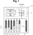
- Flash storage device 100includes a controller 101 and a number of non-volatile data blocks 110 1 , 110 2 , 110 3 , 110 4 , 110 5 , 110 6 . . . 110 n .
- data blockis used throughout the description, it will be understood by those of skill in the art that the term data block is frequently used interchangeably with the term “memory block” in the art.
- Each data blockhas a plurality of data segments for storing data, such as data segment 121 . In the present exemplary flash storage device, each data block is illustrated as including 8 data segments.
- a data blockmay be configured with more or less than 8 data segments as desired to provide various levels of storage space.
- a data blockmay include 32 data segments of 4 kilobytes (kB) each to provide 128 kB of data storage.
- data blocksare usually configured with 2 n data segments (e.g., 16, 32, 64, 128, 256, etc.), the scope of the invention is not so limited.
- each data block 110 1 - 110 nis illustrated as including the same number of data segments, the scope of the invention is not so limited, as a flash storage device may comprise a number of data blocks with differing capacities and/or numbers of data segments.
- a data blockmay span over more than one flash memory chip in a storage array of multiple chips.
- a data blockis stored on a single flash memory chip in a storage array of multiple flash memory chips.
- Controller 101includes a bus 131 or other communication mechanism for communicating information, and a processor 132 coupled with bus 131 for processing information. Controller 101 also includes a volatile memory such as random access memory (RAM) 133 coupled to bus 131 for storing information and instructions to be executed by processor 132 . RAM 133 may also be used for storing temporary variables or other intermediate information during execution of instructions by processor 132 . According to one aspect of the subject disclosure, RAM 133 may comprise one or more DRAM or RAM modules. Controller 101 may be coupled via I/O module 134 to data blocks 110 1 - 110 n , and to an external system with which flash storage device 100 communicates.
- RAMrandom access memory
- a host systemmay send and receive data to and from the flash storage device 100 in data sectors.
- each data sectormay be 512 bytes in size with eight data sectors per 4 K byte data segment.
- data sectorssuch as data sector 122 , are illustrated in FIG. 1 as about half the size of a data segment (e.g., two 512 byte data sectors per 1K data segment).
- the particular size of a data sectoris usually determined by the host device to which a flash storage device is attached.
- Some host devicesutilize data sectors with a size of 2 n bits, where n is a positive integer (e.g., 32 bits, 64 bits, 128 bits, 256 bits, 512 bits, 1024 bits, 2048 bits, etc.).
- Other host devicesuse data sectors with non-standard sizes other than 2 n bits, such as 520 bits, 524 bits, 528 bits, etc.
- n bitse.g., 1K, 2K, 4K, 8K, 16K, etc.
- FIG. 2illustrates a flash storage device in which larger, non-standard size data sectors are inefficiently stored.
- Flash storage device 200includes a controller 201 and a number of non-volatile data blocks 210 1 , 210 2 , 210 3 , 210 4 , 210 5 , 210 6 . . . 210 n .
- Controller 201includes a bus 231 or other communication mechanism for communicating information, and a processor 232 coupled with bus 231 for processing information.
- Controller 201also includes a volatile memory such as random access memory (RAM) 233 coupled to bus 231 for storing information and instructions to be executed by processor 232 .
- RAMrandom access memory
- Controller 201may be coupled via I/O module 234 to data blocks 210 1 - 210 n , and to an external system with which flash storage device 200 communicates.
- Each data block 210 1 - 210 nhas a plurality of data segments for storing data, such as data segment 221 .
- data segment 221As can be seen with reference to FIG. 2 , storing a larger, non-standard size data sector such as data sector 222 in a data segment leaves a significant portion of the storage space of the data segment unused.
- data sector 222were a 520 byte data sector
- the data segments of flash storage device 200were capable of storing 1K of data
- storing a single data sector in one data segmentwould waste 504 bytes of storage space. While some of that storage space might be used to store LBA information or ECC information corresponding to the data sector, the inefficiency of this storage system would still reduce the host-addressable storage space of flash storage device 200 by more than 40%.
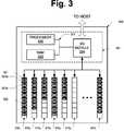
- FIG. 3illustrates a flash storage device so configured, in accordance with one aspect of the subject disclosure.
- Flash storage device 300includes a controller 301 and a number of non-volatile data blocks 310 1 , 310 2 , 310 3 , 310 4 , 310 5 , 310 6 . . . 310 n .
- Controller 301includes a bus 331 or other communication mechanism for communicating information, and a processor 332 coupled with bus 331 for processing information.
- Controller 301also includes a volatile memory such as random access memory (RAM) 333 coupled to bus 331 for storing information and instructions to be executed by processor 332 . Controller 301 may be coupled via I/O module 334 to data blocks 310 1 - 310 n , and to an external system with which flash storage device 300 communicates. Each data block 310 1 - 310 n has a plurality of data segments for storing data, such as data segment 321 . As can be seen with reference to FIG. 3 , a data segment may include multiple whole and/or partial data sectors to more efficiently utilize the space therein. For example, data segment 321 includes a whole data sector and a portion 323 a of a second data sector. The remaining portion 323 b of the second data sector is written to an adjacent or subsequent data segment, such that both portions span the boundary between the data segments.
- RAMrandom access memory
- Controller 301may be configured to cache a data segment's worth of data sectors in a buffer and then write the contents of the buffer to a desired physical page.
- controller 301may be configured to begin caching a data sector, such as the data sector of which portion 323 a is a part, and to stop adding information from that data sector to the buffer once the buffer is filled (e.g., once portion 323 a is added to the cache).
- controller 301may be configured to copy the contents of the buffer (e.g., one or more complete data sectors and portion 323 a ) to data segment 321 , to clear the buffer, and to resume caching information from the data sector where it previously left off.
- controller 301may be configured to cache information from the data sector of which portion 323 a and 323 b are parts beginning with portion 323 b . Controller 301 continues in this fashion to copy information from multiple data sectors received from a host device into a buffer until the buffer is full, to copy the buffer to a data segment, to erase the buffer, and to resume caching where it left off.
- flash storage device 300may further include a buffer operably coupled to data blocks 310 1 - 310 n .
- the buffermay be the same size as the data segments of data blocks 310 1 - 310 n , and receives data to be written to a particular data segment therein from controller 301 .
- the bufferacts as an intermediary between controller 301 and data blocks 310 1 - 310 n , inasmuch as controller 301 sends data to be written to a particular data segment to buffer 340 , which in turn copies the data to the desired data segment.
- the buffermay be provided on a flash memory chip in which data blocks 310 1 - 310 n are disposed.
- each flash memory chip in an array of memory chipsmay have a buffer for interfacing with the data blocks of the chip on which it is provided.
- the buffermay be implemented in RAM 333 .
- controller 301configuring controller 301 in this fashion allows controller 301 to treat each data block as a continuous media, greatly improving the efficiency with which the space available in a data block is utilized.
- an addressing tablemay be maintained in RAM 333 , where logical addresses (e.g., LBAs) for each data sector are correlated with physical locations in the array of data blocks.
- the addressing tablemay be configured to maintain for each data sector an identifier indicating in which data block it is stored, and an ordinal number indicating its position in the data block.
- data sector 321may be associated with an indicator indicating that it is stored in data block 310 1 , and the ordinal number 0 indicating that it is offset 0 bytes from the first position in the data block.
- the data sector of which portions 323 a and 323 b are partsmay be associated with an indicator indicating that it is stored in data block 310 1 , and the ordinal number 1, which indicates it is offset 1 data sector's worth of bytes from a first position in the data block.
- the number of bytes in a data sectormay be provided to controller 301 a priori, it is a trivial matter for controller 301 to calculate a particular physical address in data block 310 1 where this data sector begins.
- controller 301is further aware of the location of the boundaries between adjacent data segments in data block 310 1 , when controller 301 is requested to read the data in the data sector of which portions 323 a and 323 b are parts, controller 301 may read the relevant regions of data segment 321 and the following data segment (in which portion 323 b is stored) and reconstruct the data sector from portions 323 a and 323 b.
- the addressing table in RAM 333can easily locate the data thereof with only the indicator and offset described in greater detail above.
- data from a data sector which does not all fit within a single data segmentmay be split between non-adjacent data segments, and the addressing table provided with multiple indicators indicating the location of each portion.
- a flash storage devicemay also be configured to write error correction information (e.g., ECC data) corresponding to each data sector in the same data segment in which the data sector is written.
- ECC dataerror correction information
- the flash storage devicemay be configured to write the error correction information to the data segment in which the last portion of the data sector is written.
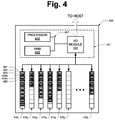
- FIG. 4illustrates one such flash storage device in accordance with one aspect of the subject disclosure.
- Flash storage device 400includes a controller 401 and a number of non-volatile data blocks 410 1 , 410 2 , 410 3 , 410 4 , 410 5 , 410 6 .
- Controller 401includes a bus 431 or other communication mechanism for communicating information, and a processor 432 coupled with bus 431 for processing information. Controller 401 also includes a volatile memory such as random access memory (RAM) 433 coupled to bus 431 for storing information and instructions to be executed by processor 432 . Controller 401 may be coupled via I/O module 434 to data blocks 410 1 - 410 n , and to an external system with which flash storage device 400 communicates. Each data block 410 1 - 410 n has a plurality of data segments for storing data, such as data segment 421 .
- RAMrandom access memory
- a data segmentmay include multiple whole and/or partial data sectors to more efficiently utilize the space therein.
- data segment 421includes a whole data sector 422 and a portion 424 a of a second data sector. The remaining portion 424 b of the second data sector is written to an adjacent or subsequent data segment, such that both portions span the boundary between the data segments.
- a data segmentmay include error correction information corresponding to a data sector stored either entirely or partially therein.
- datamay be written to the array of data blocks 410 1 - 410 n on a segment-by-segment level (e.g., in many flash storage devices, the data segment is the smallest unit of flash memory which can be written in a single operation).
- a segment-by-segment levele.g., in many flash storage devices, the data segment is the smallest unit of flash memory which can be written in a single operation.
- controller 401may be configured to cache a first data sector 422 in the buffer, to generate error correction information 423 based on the first data sector 422 and cache the error correction information 423 in the buffer, to begin caching a second data sector, such as the data sector of which portion 424 a is a part, to generate error correction information based on portion 424 a , and to stop adding information from that data sector to the buffer once the buffer is filled (e.g., once portion 424 a is added to the cache).
- controller 401may be configured to copy the contents of the buffer to a data segment, such as data segment 421 , to clear the buffer, and to resume caching information from the data sector where it previously left off.
- controller 401may be configured to cache information from the data sector of which portion 424 a and 424 b are parts, beginning with portion 424 b , and to continue generating error correction information based on portion 424 b .
- portion 424 bis finished caching, and the error correction information 425 pertaining to the data sector of which portions 424 a and 424 b are parts, error correction information 425 is cached and, when the buffer is full, the next data segment is written.
- Controller 401continues in this fashion to copy information from multiple data sectors received from a host device into a buffer, together with error correction information pertaining thereto, until the buffer is full, to copy the buffer to a data segment, to erase the buffer, and to resume caching and generating error correction information where it left off.
- FIG. 5is a flow chart illustrating a method of writing data in a flash storage device in accordance with one aspect of the subject disclosure.
- the methodbegins with step 501 , in which a plurality of data sectors to be written are cached in a system memory of the flash storage device.
- step 502a first one of the plurality of data sectors is written to a first data segment.
- step 503error correction information corresponding to the first portion of the second one of the plurality of data sectors is calculated.
- a first portion of a second one of the plurality of data sectorsis written to the first data segment.
- error correction information corresponding to the second portion of the second one of the plurality of data sectorsis calculated.
- step 506a second portion of the second one of the plurality of data sectors is written to a second data segment.
- step 507the error correction information corresponding to the first and second portions of the second one of the plurality of data sectors is written to the second data segment.
- step 508an addressing table correlating, for each of the plurality of data sectors, a logical address thereof with a physical location thereof in a corresponding one of a plurality of data blocks is updated.
- writing data in a flash storage devicemay be performed by controller 401 in response to processor 432 executing one or more sequences of one or more instructions contained in a machine-readable media, such as RAM 433 , or another volatile or non-volatile media, according to one aspect of the present invention.
- a machine-readable mediasuch as RAM 433 , or another volatile or non-volatile media
- Such instructionsmay be read into the machine-readable media from another medium, such as through I/O module 434 .
- Execution of the sequences of instructions contained in the machine-readable mediacauses processor 432 to perform the process steps described herein.
- processors in a multi-processing arrangementmay also be employed to execute the sequences of instructions contained in the machine-readable media.
- hard-wired circuitrymay be used in place of or in combination with software instructions to implement various embodiments of the present invention.
- embodiments of the present inventionare not limited to any specific combination of hardware circuitry and software.
Landscapes
- Engineering & Computer Science (AREA)
- Theoretical Computer Science (AREA)
- Physics & Mathematics (AREA)
- General Engineering & Computer Science (AREA)
- General Physics & Mathematics (AREA)
- Human Computer Interaction (AREA)
- Quality & Reliability (AREA)
- Techniques For Improving Reliability Of Storages (AREA)
- Information Retrieval, Db Structures And Fs Structures Therefor (AREA)
Abstract
Description
Claims (30)
Priority Applications (1)
| Application Number | Priority Date | Filing Date | Title |
|---|---|---|---|
| US12/492,103US8572308B2 (en) | 2008-06-25 | 2009-06-25 | Supporting variable sector sizes in flash storage devices |
Applications Claiming Priority (2)
| Application Number | Priority Date | Filing Date | Title |
|---|---|---|---|
| US7570908P | 2008-06-25 | 2008-06-25 | |
| US12/492,103US8572308B2 (en) | 2008-06-25 | 2009-06-25 | Supporting variable sector sizes in flash storage devices |
Publications (2)
| Publication Number | Publication Date |
|---|---|
| US20100042901A1 US20100042901A1 (en) | 2010-02-18 |
| US8572308B2true US8572308B2 (en) | 2013-10-29 |
Family
ID=41448931
Family Applications (10)
| Application Number | Title | Priority Date | Filing Date |
|---|---|---|---|
| US12/343,378Active2031-03-24US8843691B2 (en) | 2008-06-25 | 2008-12-23 | Prioritized erasure of data blocks in a flash storage device |
| US12/464,856AbandonedUS20090327804A1 (en) | 2008-06-25 | 2009-05-12 | Wear leveling in flash storage devices |
| US12/492,113Active2030-09-13US8825941B2 (en) | 2008-06-25 | 2009-06-25 | SLC-MLC combination flash storage device |
| US12/492,104Active2030-06-04US9311006B2 (en) | 2008-06-25 | 2009-06-25 | Table journaling in flash storage devices |
| US12/492,103Active2032-03-16US8572308B2 (en) | 2008-06-25 | 2009-06-25 | Supporting variable sector sizes in flash storage devices |
| US12/492,110AbandonedUS20120239853A1 (en) | 2008-06-25 | 2009-06-25 | Solid state device with allocated flash cache |
| US12/492,109Active2030-06-15US9043531B2 (en) | 2008-06-25 | 2009-06-25 | High speed input/output performance in solid state devices |
| US12/492,112Active2030-08-02US8762622B2 (en) | 2008-06-25 | 2009-06-25 | Enhanced MLC solid state device |
| US12/492,107Active2031-07-07US8347138B2 (en) | 2008-06-25 | 2009-06-25 | Redundant data distribution in a flash storage device |
| US14/720,697ActiveUS9411522B2 (en) | 2008-06-25 | 2015-05-22 | High speed input/output performance in solid state devices |
Family Applications Before (4)
| Application Number | Title | Priority Date | Filing Date |
|---|---|---|---|
| US12/343,378Active2031-03-24US8843691B2 (en) | 2008-06-25 | 2008-12-23 | Prioritized erasure of data blocks in a flash storage device |
| US12/464,856AbandonedUS20090327804A1 (en) | 2008-06-25 | 2009-05-12 | Wear leveling in flash storage devices |
| US12/492,113Active2030-09-13US8825941B2 (en) | 2008-06-25 | 2009-06-25 | SLC-MLC combination flash storage device |
| US12/492,104Active2030-06-04US9311006B2 (en) | 2008-06-25 | 2009-06-25 | Table journaling in flash storage devices |
Family Applications After (5)
| Application Number | Title | Priority Date | Filing Date |
|---|---|---|---|
| US12/492,110AbandonedUS20120239853A1 (en) | 2008-06-25 | 2009-06-25 | Solid state device with allocated flash cache |
| US12/492,109Active2030-06-15US9043531B2 (en) | 2008-06-25 | 2009-06-25 | High speed input/output performance in solid state devices |
| US12/492,112Active2030-08-02US8762622B2 (en) | 2008-06-25 | 2009-06-25 | Enhanced MLC solid state device |
| US12/492,107Active2031-07-07US8347138B2 (en) | 2008-06-25 | 2009-06-25 | Redundant data distribution in a flash storage device |
| US14/720,697ActiveUS9411522B2 (en) | 2008-06-25 | 2015-05-22 | High speed input/output performance in solid state devices |
Country Status (1)
| Country | Link |
|---|---|
| US (10) | US8843691B2 (en) |
Families Citing this family (406)
| Publication number | Priority date | Publication date | Assignee | Title |
|---|---|---|---|---|
| US8489817B2 (en) | 2007-12-06 | 2013-07-16 | Fusion-Io, Inc. | Apparatus, system, and method for caching data |
| US8443134B2 (en) | 2006-12-06 | 2013-05-14 | Fusion-Io, Inc. | Apparatus, system, and method for graceful cache device degradation |
| US8019938B2 (en) | 2006-12-06 | 2011-09-13 | Fusion-I0, Inc. | Apparatus, system, and method for solid-state storage as cache for high-capacity, non-volatile storage |
| US9104599B2 (en) | 2007-12-06 | 2015-08-11 | Intelligent Intellectual Property Holdings 2 Llc | Apparatus, system, and method for destaging cached data |
| US8706968B2 (en) | 2007-12-06 | 2014-04-22 | Fusion-Io, Inc. | Apparatus, system, and method for redundant write caching |
| US7852654B2 (en)* | 2006-12-28 | 2010-12-14 | Hynix Semiconductor Inc. | Semiconductor memory device, and multi-chip package and method of operating the same |
| JP5171448B2 (en)* | 2007-07-31 | 2013-03-27 | キヤノン株式会社 | Image forming apparatus and control method thereof |
| US7975105B1 (en)* | 2007-12-03 | 2011-07-05 | Yingju Sun | Solid state storage devices with changeable capacity |
| US9519540B2 (en) | 2007-12-06 | 2016-12-13 | Sandisk Technologies Llc | Apparatus, system, and method for destaging cached data |
| US7836226B2 (en) | 2007-12-06 | 2010-11-16 | Fusion-Io, Inc. | Apparatus, system, and method for coordinating storage requests in a multi-processor/multi-thread environment |
| KR101077339B1 (en)* | 2007-12-28 | 2011-10-26 | 가부시끼가이샤 도시바 | Semiconductor storage device |
| US8843691B2 (en) | 2008-06-25 | 2014-09-23 | Stec, Inc. | Prioritized erasure of data blocks in a flash storage device |
| US8891298B2 (en) | 2011-07-19 | 2014-11-18 | Greenthread, Llc | Lifetime mixed level non-volatile memory system |
| JP5192352B2 (en)* | 2008-10-30 | 2013-05-08 | 株式会社日立製作所 | Storage device and data storage area management method |
| TWI385672B (en)* | 2008-11-05 | 2013-02-11 | Lite On It Corp | Adaptive multi-channel controller and method for storage device |
| US8239613B2 (en)* | 2008-12-30 | 2012-08-07 | Intel Corporation | Hybrid memory device |
| TWI385527B (en)* | 2009-02-10 | 2013-02-11 | Phison Electronics Corp | Multi level cell nand flash memory storage system, and controller and accessing method thereof |
| KR20100097456A (en)* | 2009-02-26 | 2010-09-03 | 삼성전자주식회사 | Memory system and address allocating method of flash translation layer thereof |
| US8261158B2 (en) | 2009-03-13 | 2012-09-04 | Fusion-Io, Inc. | Apparatus, system, and method for using multi-level cell solid-state storage as single level cell solid-state storage |
| US8266503B2 (en) | 2009-03-13 | 2012-09-11 | Fusion-Io | Apparatus, system, and method for using multi-level cell storage in a single-level cell mode |
| KR101581679B1 (en)* | 2009-03-18 | 2015-12-31 | 삼성전자주식회사 | Storage device and method for managing buffer memory of storage device |
| US8195891B2 (en)* | 2009-03-30 | 2012-06-05 | Intel Corporation | Techniques to perform power fail-safe caching without atomic metadata |
| US8171219B2 (en)* | 2009-03-31 | 2012-05-01 | Intel Corporation | Method and system to perform caching based on file-level heuristics |
| US8341501B2 (en)* | 2009-04-30 | 2012-12-25 | International Business Machines Corporation | Adaptive endurance coding of non-volatile memories |
| US20100318746A1 (en)* | 2009-06-12 | 2010-12-16 | Seakr Engineering, Incorporated | Memory change track logging |
| US20100332726A1 (en)* | 2009-06-26 | 2010-12-30 | Solid State System Co., Ltd. | Structure and method for managing writing operation on mlc flash memory |
| US20100332922A1 (en)* | 2009-06-30 | 2010-12-30 | Mediatek Inc. | Method for managing device and solid state disk drive utilizing the same |
| US8510497B2 (en)* | 2009-07-29 | 2013-08-13 | Stec, Inc. | Flash storage device with flexible data format |
| US7941696B2 (en)* | 2009-08-11 | 2011-05-10 | Texas Memory Systems, Inc. | Flash-based memory system with static or variable length page stripes including data protection information and auxiliary protection stripes |
| US7856528B1 (en)* | 2009-08-11 | 2010-12-21 | Texas Memory Systems, Inc. | Method and apparatus for protecting data using variable size page stripes in a FLASH-based storage system |
| US8930622B2 (en) | 2009-08-11 | 2015-01-06 | International Business Machines Corporation | Multi-level data protection for flash memory system |
| US7818525B1 (en)* | 2009-08-12 | 2010-10-19 | Texas Memory Systems, Inc. | Efficient reduction of read disturb errors in NAND FLASH memory |
| US8189379B2 (en) | 2009-08-12 | 2012-05-29 | Texas Memory Systems, Inc. | Reduction of read disturb errors in NAND FLASH memory |
| JP5002629B2 (en)* | 2009-08-28 | 2012-08-15 | 株式会社東芝 | Memory system |
| JP5999645B2 (en) | 2009-09-08 | 2016-10-05 | ロンギチュード エンタープライズ フラッシュ エスエイアールエル | Apparatus, system, and method for caching data on a solid state storage device |
| US9122579B2 (en) | 2010-01-06 | 2015-09-01 | Intelligent Intellectual Property Holdings 2 Llc | Apparatus, system, and method for a storage layer |
| KR101769883B1 (en) | 2009-09-09 | 2017-08-21 | 샌디스크 테크놀로지스 엘엘씨 | Apparatus, system, and method for allocating storage |
| US8489804B1 (en)* | 2009-09-14 | 2013-07-16 | Marvell International Ltd. | System for using dynamic random access memory to reduce the effect of write amplification in flash memory |
| US8990476B2 (en)* | 2009-10-01 | 2015-03-24 | Micron Technology, Inc. | Power interrupt management |
| US8214700B2 (en)* | 2009-10-28 | 2012-07-03 | Sandisk Technologies Inc. | Non-volatile memory and method with post-write read and adaptive re-write to manage errors |
| US8423866B2 (en)* | 2009-10-28 | 2013-04-16 | SanDisk Technologies, Inc. | Non-volatile memory and method with post-write read and adaptive re-write to manage errors |
| US8634240B2 (en)* | 2009-10-28 | 2014-01-21 | SanDisk Technologies, Inc. | Non-volatile memory and method with accelerated post-write read to manage errors |
| US8560770B2 (en)* | 2009-11-13 | 2013-10-15 | Seagate Technology Llc | Non-volatile write cache for a data storage system |
| US8176235B2 (en)* | 2009-12-04 | 2012-05-08 | International Business Machines Corporation | Non-volatile memories with enhanced write performance and endurance |
| US8285918B2 (en)* | 2009-12-11 | 2012-10-09 | Nimble Storage, Inc. | Flash memory cache for data storage device |
| US9128762B2 (en) | 2009-12-15 | 2015-09-08 | Micron Technology, Inc. | Persistent content in nonvolatile memory |
| TWI497293B (en)* | 2009-12-17 | 2015-08-21 | Ibm | Data management in solid state storage devices |
| US8473808B2 (en)* | 2010-01-26 | 2013-06-25 | Qimonda Ag | Semiconductor memory having non-standard form factor |
| US8661184B2 (en) | 2010-01-27 | 2014-02-25 | Fusion-Io, Inc. | Managing non-volatile media |
| US8854882B2 (en) | 2010-01-27 | 2014-10-07 | Intelligent Intellectual Property Holdings 2 Llc | Configuring storage cells |
| US9245653B2 (en) | 2010-03-15 | 2016-01-26 | Intelligent Intellectual Property Holdings 2 Llc | Reduced level cell mode for non-volatile memory |
| US8725931B1 (en) | 2010-03-26 | 2014-05-13 | Western Digital Technologies, Inc. | System and method for managing the execution of memory commands in a solid-state memory |
| US8713066B1 (en)* | 2010-03-29 | 2014-04-29 | Western Digital Technologies, Inc. | Managing wear leveling and garbage collection operations in a solid-state memory using linked lists |
| JP2011209973A (en)* | 2010-03-30 | 2011-10-20 | Hitachi Ltd | Disk array configuration program, computer and computer system |
| US8751740B1 (en)* | 2010-03-31 | 2014-06-10 | Emc Corporation | Systems, methods, and computer readable media for performance optimization of storage allocation to virtual logical units |
| US8621141B2 (en)* | 2010-04-01 | 2013-12-31 | Intel Corporations | Method and system for wear leveling in a solid state drive |
| WO2011133145A1 (en)* | 2010-04-21 | 2011-10-27 | Hewlett-Packard Development Company, L.P. | Communicating operating system booting information |
| US8782327B1 (en) | 2010-05-11 | 2014-07-15 | Western Digital Technologies, Inc. | System and method for managing execution of internal commands and host commands in a solid-state memory |
| US9026716B2 (en)* | 2010-05-12 | 2015-05-05 | Western Digital Technologies, Inc. | System and method for managing garbage collection in solid-state memory |
| US8959300B2 (en) | 2010-05-18 | 2015-02-17 | International Business Machines Corporation | Cascade ordering |
| US8886870B2 (en)* | 2010-05-25 | 2014-11-11 | Marvell World Trade Ltd. | Memory access table saving and restoring system and methods |
| US8966176B2 (en) | 2010-05-27 | 2015-02-24 | Sandisk Il Ltd. | Memory management storage to a host device |
| US9043533B1 (en)* | 2010-06-29 | 2015-05-26 | Emc Corporation | Sizing volatile memory cache based on flash-based cache usage |
| US8656256B2 (en)* | 2010-07-07 | 2014-02-18 | Stec, Inc. | Apparatus and method for multi-mode operation of a flash memory device |
| JPWO2012020544A1 (en)* | 2010-08-11 | 2013-10-28 | 日本電気株式会社 | Data processing system, data processing method, and program |
| US12008266B2 (en) | 2010-09-15 | 2024-06-11 | Pure Storage, Inc. | Efficient read by reconstruction |
| US11614893B2 (en) | 2010-09-15 | 2023-03-28 | Pure Storage, Inc. | Optimizing storage device access based on latency |
| US8417878B2 (en) | 2010-09-20 | 2013-04-09 | Seagate Technology Llc | Selection of units for garbage collection in flash memory |
| US9021192B1 (en) | 2010-09-21 | 2015-04-28 | Western Digital Technologies, Inc. | System and method for enhancing processing of memory access requests |
| US9164886B1 (en) | 2010-09-21 | 2015-10-20 | Western Digital Technologies, Inc. | System and method for multistage processing in a memory storage subsystem |
| WO2012039983A1 (en) | 2010-09-24 | 2012-03-29 | Rambus Inc. | Memory device with ecc history table |
| TWI425357B (en) | 2010-09-27 | 2014-02-01 | Silicon Motion Inc | Method for performing block management, and associated memory device and controller thereof |
| TWI435216B (en)* | 2010-09-27 | 2014-04-21 | Silicon Motion Inc | Method for performing meta block management, and associated memory device and controller thereof |
| US8612804B1 (en) | 2010-09-30 | 2013-12-17 | Western Digital Technologies, Inc. | System and method for improving wear-leveling performance in solid-state memory |
| IL208641A0 (en)* | 2010-10-12 | 2010-12-30 | Eci Telecom Ltd | Method for accelerating start up of a computerized system |
| US8769374B2 (en) | 2010-10-13 | 2014-07-01 | International Business Machines Corporation | Multi-write endurance and error control coding of non-volatile memories |
| JP2012108627A (en)* | 2010-11-15 | 2012-06-07 | Toshiba Corp | Memory system |
| US8949502B2 (en)* | 2010-11-18 | 2015-02-03 | Nimble Storage, Inc. | PCIe NVRAM card based on NVDIMM |
| US8089807B1 (en) | 2010-11-22 | 2012-01-03 | Ge Aviation Systems, Llc | Method and system for data storage |
| CN102479156B (en)* | 2010-11-22 | 2015-03-11 | 慧荣科技股份有限公司 | Method for block management, memory device and controller thereof |
| US8495338B2 (en) | 2010-12-03 | 2013-07-23 | Micron Technology, Inc. | Transaction log recovery |
| KR101936311B1 (en)* | 2010-12-03 | 2019-01-09 | 삼성전자주식회사 | Method of processing data |
| US20120239860A1 (en) | 2010-12-17 | 2012-09-20 | Fusion-Io, Inc. | Apparatus, system, and method for persistent data management on a non-volatile storage media |
| US9268646B1 (en)* | 2010-12-21 | 2016-02-23 | Western Digital Technologies, Inc. | System and method for optimized management of operation data in a solid-state memory |
| US9092337B2 (en) | 2011-01-31 | 2015-07-28 | Intelligent Intellectual Property Holdings 2 Llc | Apparatus, system, and method for managing eviction of data |
| US8909851B2 (en) | 2011-02-08 | 2014-12-09 | SMART Storage Systems, Inc. | Storage control system with change logging mechanism and method of operation thereof |
| US9003104B2 (en) | 2011-02-15 | 2015-04-07 | Intelligent Intellectual Property Holdings 2 Llc | Systems and methods for a file-level cache |
| US9201677B2 (en) | 2011-05-23 | 2015-12-01 | Intelligent Intellectual Property Holdings 2 Llc | Managing data input/output operations |
| US8874823B2 (en) | 2011-02-15 | 2014-10-28 | Intellectual Property Holdings 2 Llc | Systems and methods for managing data input/output operations |
| WO2012116369A2 (en) | 2011-02-25 | 2012-08-30 | Fusion-Io, Inc. | Apparatus, system, and method for managing contents of a cache |
| US8966191B2 (en) | 2011-03-18 | 2015-02-24 | Fusion-Io, Inc. | Logical interface for contextual storage |
| US9563555B2 (en) | 2011-03-18 | 2017-02-07 | Sandisk Technologies Llc | Systems and methods for storage allocation |
| US8935466B2 (en) | 2011-03-28 | 2015-01-13 | SMART Storage Systems, Inc. | Data storage system with non-volatile memory and method of operation thereof |
| KR101800444B1 (en)* | 2011-03-28 | 2017-12-20 | 삼성전자주식회사 | Control method of nonvolatile memory and memory system including the same |
| US9361044B2 (en) | 2011-03-28 | 2016-06-07 | Western Digital Technologies, Inc. | Power-safe data management system |
| KR101810932B1 (en)* | 2011-04-27 | 2017-12-20 | 시게이트 테크놀로지 엘엘씨 | Method for managing address mapping information, accessing method of disk drive, method for managing address mapping information via network, and storage device, computer system and storage medium applying the same |
| US8886911B2 (en) | 2011-05-31 | 2014-11-11 | Micron Technology, Inc. | Dynamic memory cache size adjustment in a memory device |
| US8792273B2 (en) | 2011-06-13 | 2014-07-29 | SMART Storage Systems, Inc. | Data storage system with power cycle management and method of operation thereof |
| US8898373B1 (en) | 2011-06-29 | 2014-11-25 | Western Digital Technologies, Inc. | System and method for improving wear-leveling performance in solid-state memory |
| US9003101B1 (en) | 2011-06-29 | 2015-04-07 | Western Digital Technologies, Inc. | Prioritized access for media with heterogeneous access rates |
| US9158670B1 (en) | 2011-06-30 | 2015-10-13 | Western Digital Technologies, Inc. | System and method for dynamically adjusting garbage collection policies in solid-state memory |
| US20130007373A1 (en)* | 2011-06-30 | 2013-01-03 | Advanced Micro Devices, Inc. | Region based cache replacement policy utilizing usage information |
| US9318166B2 (en) | 2011-07-22 | 2016-04-19 | SanDisk Technologies, Inc. | Systems and methods of storing data |
| US8726104B2 (en) | 2011-07-28 | 2014-05-13 | Sandisk Technologies Inc. | Non-volatile memory and method with accelerated post-write read using combined verification of multiple pages |
| KR101861170B1 (en) | 2011-08-17 | 2018-05-25 | 삼성전자주식회사 | Memory system including migration manager |
| US9098399B2 (en) | 2011-08-31 | 2015-08-04 | SMART Storage Systems, Inc. | Electronic system with storage management mechanism and method of operation thereof |
| US9021231B2 (en) | 2011-09-02 | 2015-04-28 | SMART Storage Systems, Inc. | Storage control system with write amplification control mechanism and method of operation thereof |
| US9063844B2 (en) | 2011-09-02 | 2015-06-23 | SMART Storage Systems, Inc. | Non-volatile memory management system with time measure mechanism and method of operation thereof |
| US9021319B2 (en) | 2011-09-02 | 2015-04-28 | SMART Storage Systems, Inc. | Non-volatile memory management system with load leveling and method of operation thereof |
| CN102279808A (en)* | 2011-09-06 | 2011-12-14 | 晨星软件研发(深圳)有限公司 | Method and device for managing video memory of embedded equipment |
| US9298603B2 (en)* | 2011-09-09 | 2016-03-29 | OCZ Storage Solutions Inc. | NAND flash-based storage device and methods of using |
| US20130066882A1 (en)* | 2011-09-09 | 2013-03-14 | Onzo Limited | Data storage method and system |
| US9588883B2 (en)* | 2011-09-23 | 2017-03-07 | Conversant Intellectual Property Management Inc. | Flash memory system |
| US9367453B1 (en)* | 2011-09-30 | 2016-06-14 | Emc Corporation | System and method for migrating cache data |
| US9367452B1 (en)* | 2011-09-30 | 2016-06-14 | Emc Corporation | System and method for apportioning storage |
| US8635407B2 (en)* | 2011-09-30 | 2014-01-21 | International Business Machines Corporation | Direct memory address for solid-state drives |
| US20130086300A1 (en)* | 2011-10-04 | 2013-04-04 | Lsi Corporation | Storage caching acceleration through usage of r5 protected fast tier |
| US8539007B2 (en) | 2011-10-17 | 2013-09-17 | International Business Machines Corporation | Efficient garbage collection in a compressed journal file |
| US8949553B2 (en) | 2011-10-28 | 2015-02-03 | Dell Products L.P. | System and method for retention of historical data in storage resources |
| US8977803B2 (en)* | 2011-11-21 | 2015-03-10 | Western Digital Technologies, Inc. | Disk drive data caching using a multi-tiered memory |
| US9240240B2 (en)* | 2011-11-29 | 2016-01-19 | Micron Technology, Inc. | Apparatus having indications of memory cell density and methods of their determination and use |
| KR101893145B1 (en) | 2011-12-06 | 2018-10-05 | 삼성전자주식회사 | Memory systems and block copy methods thereof |
| US9274937B2 (en) | 2011-12-22 | 2016-03-01 | Longitude Enterprise Flash S.A.R.L. | Systems, methods, and interfaces for vector input/output operations |
| US9176862B2 (en) | 2011-12-29 | 2015-11-03 | Sandisk Technologies Inc. | SLC-MLC wear balancing |
| WO2013100783A1 (en) | 2011-12-29 | 2013-07-04 | Intel Corporation | Method and system for control signalling in a data path module |
| US9251052B2 (en) | 2012-01-12 | 2016-02-02 | Intelligent Intellectual Property Holdings 2 Llc | Systems and methods for profiling a non-volatile cache having a logical-to-physical translation layer |
| US9767032B2 (en) | 2012-01-12 | 2017-09-19 | Sandisk Technologies Llc | Systems and methods for cache endurance |
| US8782344B2 (en) | 2012-01-12 | 2014-07-15 | Fusion-Io, Inc. | Systems and methods for managing cache admission |
| US20130185503A1 (en)* | 2012-01-12 | 2013-07-18 | Vigneshwara Bhatta | Method for metadata persistence |
| US10102117B2 (en) | 2012-01-12 | 2018-10-16 | Sandisk Technologies Llc | Systems and methods for cache and storage device coordination |
| US9251086B2 (en) | 2012-01-24 | 2016-02-02 | SanDisk Technologies, Inc. | Apparatus, system, and method for managing a cache |
| US9116812B2 (en) | 2012-01-27 | 2015-08-25 | Intelligent Intellectual Property Holdings 2 Llc | Systems and methods for a de-duplication cache |
| US10359972B2 (en) | 2012-08-31 | 2019-07-23 | Sandisk Technologies Llc | Systems, methods, and interfaces for adaptive persistence |
| US8898423B1 (en)* | 2012-01-31 | 2014-11-25 | Western Digital Technologies, Inc. | High performance caching architecture for data storage systems |
| US9223686B1 (en)* | 2012-02-01 | 2015-12-29 | Amazon Technologies, Inc. | Cache memory data storage control system and method |
| US9239781B2 (en) | 2012-02-07 | 2016-01-19 | SMART Storage Systems, Inc. | Storage control system with erase block mechanism and method of operation thereof |
| KR101923157B1 (en) | 2012-02-22 | 2018-11-28 | 삼성전자주식회사 | Memory system and program method thereof |
| US10019353B2 (en) | 2012-03-02 | 2018-07-10 | Longitude Enterprise Flash S.A.R.L. | Systems and methods for referencing data on a storage medium |
| JP5659178B2 (en)* | 2012-03-16 | 2015-01-28 | 株式会社東芝 | NONVOLATILE MEMORY DEVICE AND NONVOLATILE MEMORY CONTROL METHOD |
| US9298252B2 (en) | 2012-04-17 | 2016-03-29 | SMART Storage Systems, Inc. | Storage control system with power down mechanism and method of operation thereof |
| US8868824B2 (en) | 2012-04-19 | 2014-10-21 | Microsoft Corporation | Solid-state drive management and control |
| US8990477B2 (en)* | 2012-04-19 | 2015-03-24 | Sandisk Technologies Inc. | System and method for limiting fragmentation |
| US9003224B2 (en) | 2012-04-25 | 2015-04-07 | Western Digital Technologies, Inc. | Managing unreliable memory in data storage systems |
| US9116792B2 (en)* | 2012-05-18 | 2015-08-25 | Silicon Motion, Inc. | Data storage device and method for flash block management |
| US20130311700A1 (en)* | 2012-05-20 | 2013-11-21 | Chung-Jwu Chen | Extending Lifetime For Non-volatile Memory Apparatus |
| US8996957B1 (en) | 2012-05-22 | 2015-03-31 | Pmc-Sierra, Inc. | Systems and methods for initializing regions of a flash drive having diverse error correction coding (ECC) schemes |
| US9021333B1 (en) | 2012-05-22 | 2015-04-28 | Pmc-Sierra, Inc. | Systems and methods for recovering data from failed portions of a flash drive |
| US9176812B1 (en) | 2012-05-22 | 2015-11-03 | Pmc-Sierra, Inc. | Systems and methods for storing data in page stripes of a flash drive |
| US9021336B1 (en) | 2012-05-22 | 2015-04-28 | Pmc-Sierra, Inc. | Systems and methods for redundantly storing error correction codes in a flash drive with secondary parity information spread out across each page of a group of pages |
| US9021337B1 (en) | 2012-05-22 | 2015-04-28 | Pmc-Sierra, Inc. | Systems and methods for adaptively selecting among different error correction coding schemes in a flash drive |
| US8972824B1 (en) | 2012-05-22 | 2015-03-03 | Pmc-Sierra, Inc. | Systems and methods for transparently varying error correction code strength in a flash drive |
| US8793556B1 (en) | 2012-05-22 | 2014-07-29 | Pmc-Sierra, Inc. | Systems and methods for reclaiming flash blocks of a flash drive |
| US9183085B1 (en) | 2012-05-22 | 2015-11-10 | Pmc-Sierra, Inc. | Systems and methods for adaptively selecting from among a plurality of error correction coding schemes in a flash drive for robustness and low latency |
| US9047214B1 (en)* | 2012-05-22 | 2015-06-02 | Pmc-Sierra, Inc. | System and method for tolerating a failed page in a flash device |
| US8788910B1 (en) | 2012-05-22 | 2014-07-22 | Pmc-Sierra, Inc. | Systems and methods for low latency, high reliability error correction in a flash drive |
| TWI477966B (en)* | 2012-05-31 | 2015-03-21 | Silicon Motion Inc | Data storage device and operating method for flash memory |
| US9195598B2 (en) | 2012-06-08 | 2015-11-24 | International Business Machines Corporation | Synchronous and asynchronous discard scans based on the type of cache memory |
| US9336150B2 (en) | 2012-06-08 | 2016-05-10 | International Business Machines Corporation | Performing asynchronous discard scans with staging and destaging operations |
| US8949689B2 (en) | 2012-06-11 | 2015-02-03 | SMART Storage Systems, Inc. | Storage control system with data management mechanism and method of operation thereof |
| US8954653B1 (en) | 2012-06-26 | 2015-02-10 | Western Digital Technologies, Inc. | Mechanisms for efficient management of system data in data storage systems |
| TWI454913B (en)* | 2012-06-26 | 2014-10-01 | Phison Electronics Corp | Data writing method, memory controller and memory storage device |
| KR101929584B1 (en)* | 2012-06-29 | 2018-12-17 | 에스케이하이닉스 주식회사 | Data storage device and operating method thereof |
| US8566671B1 (en) | 2012-06-29 | 2013-10-22 | Sandisk Technologies Inc. | Configurable accelerated post-write read to manage errors |
| US10339056B2 (en) | 2012-07-03 | 2019-07-02 | Sandisk Technologies Llc | Systems, methods and apparatus for cache transfers |
| US9612966B2 (en) | 2012-07-03 | 2017-04-04 | Sandisk Technologies Llc | Systems, methods and apparatus for a virtual machine cache |
| US8751730B2 (en)* | 2012-07-27 | 2014-06-10 | Winbond Electronics Corp. | Serial interface flash memory apparatus and writing method for status register thereof |
| US9208099B2 (en) | 2012-08-08 | 2015-12-08 | International Business Machines Corporation | Adjustment of the number of task control blocks allocated for discard scans |
| US10318495B2 (en) | 2012-09-24 | 2019-06-11 | Sandisk Technologies Llc | Snapshots for a non-volatile device |
| US10509776B2 (en) | 2012-09-24 | 2019-12-17 | Sandisk Technologies Llc | Time sequence data management |
| US9524800B2 (en) | 2012-09-26 | 2016-12-20 | International Business Machines Corporation | Performance evaluation of solid state memory device |
| US8880786B2 (en)* | 2012-09-28 | 2014-11-04 | Apple Inc. | Flash translation layer (FTL) database journaling schemes |
| KR102025263B1 (en) | 2012-10-05 | 2019-09-25 | 삼성전자주식회사 | Memory system and read reclaim method thereof |
| US9507523B1 (en) | 2012-10-12 | 2016-11-29 | Western Digital Technologies, Inc. | Methods, devices and systems for variable size logical page management in a solid state drive |
| US9489296B1 (en)* | 2012-10-17 | 2016-11-08 | Western Digital Technologies, Inc. | Methods, devices and systems for hardware-based garbage collection in solid state drives |
| US20140136575A1 (en)* | 2012-11-10 | 2014-05-15 | Yuanyuan Zhao | Log-structured garbage collection |
| US11037625B2 (en)* | 2012-11-20 | 2021-06-15 | Thstyme Bermuda Limited | Solid state drive architectures |
| MX364783B (en)* | 2012-11-20 | 2019-05-07 | Thstyme Bermuda Ltd | Solid state drive architectures. |
| US9671962B2 (en) | 2012-11-30 | 2017-06-06 | Sandisk Technologies Llc | Storage control system with data management mechanism of parity and method of operation thereof |
| CN103034603B (en)* | 2012-12-07 | 2014-06-18 | 天津瑞发科半导体技术有限公司 | Multi-channel flash memory card control device and control method thereof |
| US20150143021A1 (en)* | 2012-12-26 | 2015-05-21 | Unisys Corporation | Equalizing wear on storage devices through file system controls |
| KR20150105323A (en)* | 2013-01-08 | 2015-09-16 | 바이올린 메모리 인코포레이티드 | Method and system for data storage |
| CN103092770B (en)* | 2013-01-18 | 2015-08-12 | 山东华芯半导体有限公司 | The method of memory cost is reduced during a kind of abrasion equilibrium process |
| US9176892B2 (en)* | 2013-01-22 | 2015-11-03 | International Business Machines Corporation | Performing staging or destaging based on the number of waiting discard scans |
| US9123445B2 (en) | 2013-01-22 | 2015-09-01 | SMART Storage Systems, Inc. | Storage control system with data management mechanism and method of operation thereof |
| US20140223072A1 (en)* | 2013-02-07 | 2014-08-07 | Lsi Corporation | Tiered Caching Using Single Level Cell and Multi-Level Cell Flash Technology |
| US9329928B2 (en) | 2013-02-20 | 2016-05-03 | Sandisk Enterprise IP LLC. | Bandwidth optimization in a non-volatile memory system |
| US9214965B2 (en) | 2013-02-20 | 2015-12-15 | Sandisk Enterprise Ip Llc | Method and system for improving data integrity in non-volatile storage |
| US9183137B2 (en) | 2013-02-27 | 2015-11-10 | SMART Storage Systems, Inc. | Storage control system with data management mechanism and method of operation thereof |
| US20140250277A1 (en)* | 2013-03-04 | 2014-09-04 | Kabushiki Kaisha Toshiba | Memory system |
| US9470720B2 (en) | 2013-03-08 | 2016-10-18 | Sandisk Technologies Llc | Test system with localized heating and method of manufacture thereof |
| US9842053B2 (en) | 2013-03-15 | 2017-12-12 | Sandisk Technologies Llc | Systems and methods for persistent cache logging |
| US9208018B1 (en) | 2013-03-15 | 2015-12-08 | Pmc-Sierra, Inc. | Systems and methods for reclaiming memory for solid-state memory |
| US9026867B1 (en) | 2013-03-15 | 2015-05-05 | Pmc-Sierra, Inc. | Systems and methods for adapting to changing characteristics of multi-level cells in solid-state memory |
| US9053012B1 (en) | 2013-03-15 | 2015-06-09 | Pmc-Sierra, Inc. | Systems and methods for storing data for solid-state memory |
| US9081701B1 (en) | 2013-03-15 | 2015-07-14 | Pmc-Sierra, Inc. | Systems and methods for decoding data for solid-state memory |
| US9009565B1 (en) | 2013-03-15 | 2015-04-14 | Pmc-Sierra, Inc. | Systems and methods for mapping for solid-state memory |
| US9043780B2 (en) | 2013-03-27 | 2015-05-26 | SMART Storage Systems, Inc. | Electronic system with system modification control mechanism and method of operation thereof |
| US9170941B2 (en) | 2013-04-05 | 2015-10-27 | Sandisk Enterprises IP LLC | Data hardening in a storage system |
| US10049037B2 (en) | 2013-04-05 | 2018-08-14 | Sandisk Enterprise Ip Llc | Data management in a storage system |
| US9543025B2 (en) | 2013-04-11 | 2017-01-10 | Sandisk Technologies Llc | Storage control system with power-off time estimation mechanism and method of operation thereof |
| US10546648B2 (en) | 2013-04-12 | 2020-01-28 | Sandisk Technologies Llc | Storage control system with data management mechanism and method of operation thereof |
| US10558561B2 (en) | 2013-04-16 | 2020-02-11 | Sandisk Technologies Llc | Systems and methods for storage metadata management |
| US10102144B2 (en) | 2013-04-16 | 2018-10-16 | Sandisk Technologies Llc | Systems, methods and interfaces for data virtualization |
| US9830257B1 (en)* | 2013-06-12 | 2017-11-28 | Western Digital Technologies, Inc. | Fast saving of data during power interruption in data storage systems |
| US9313874B2 (en) | 2013-06-19 | 2016-04-12 | SMART Storage Systems, Inc. | Electronic system with heat extraction and method of manufacture thereof |
| US9898056B2 (en) | 2013-06-19 | 2018-02-20 | Sandisk Technologies Llc | Electronic assembly with thermal channel and method of manufacture thereof |
| US10331375B1 (en)* | 2013-06-21 | 2019-06-25 | Amazon Technologies, Inc. | Data storage area cleaner |
| US9244519B1 (en) | 2013-06-25 | 2016-01-26 | Smart Storage Systems. Inc. | Storage system with data transfer rate adjustment for power throttling |
| US9367353B1 (en) | 2013-06-25 | 2016-06-14 | Sandisk Technologies Inc. | Storage control system with power throttling mechanism and method of operation thereof |
| CN104298605A (en)* | 2013-07-17 | 2015-01-21 | 光宝科技股份有限公司 | Block grouping method for garbage collection action in solid-state storage device |
| CN104298465B (en)* | 2013-07-17 | 2017-06-20 | 光宝电子(广州)有限公司 | Block group technology in solid state storage device |
| US9274865B2 (en) | 2013-08-01 | 2016-03-01 | HGST Netherlands B.V. | Implementing enhanced buffer management for data storage devices |
| US9146850B2 (en) | 2013-08-01 | 2015-09-29 | SMART Storage Systems, Inc. | Data storage system with dynamic read threshold mechanism and method of operation thereof |
| US9842128B2 (en) | 2013-08-01 | 2017-12-12 | Sandisk Technologies Llc | Systems and methods for atomic storage operations |
| US9448946B2 (en) | 2013-08-07 | 2016-09-20 | Sandisk Technologies Llc | Data storage system with stale data mechanism and method of operation thereof |
| US9361222B2 (en) | 2013-08-07 | 2016-06-07 | SMART Storage Systems, Inc. | Electronic system with storage drive life estimation mechanism and method of operation thereof |
| US9431113B2 (en) | 2013-08-07 | 2016-08-30 | Sandisk Technologies Llc | Data storage system with dynamic erase block grouping mechanism and method of operation thereof |
| KR20150020385A (en)* | 2013-08-13 | 2015-02-26 | 에스케이하이닉스 주식회사 | Data storage device, operating method thereof and data processing system including the same |
| KR20150020384A (en)* | 2013-08-13 | 2015-02-26 | 에스케이하이닉스 주식회사 | Data storage device and operating method thereof |
| JP5768100B2 (en)* | 2013-09-10 | 2015-08-26 | 株式会社東芝 | MEMORY DEVICE, SERVER DEVICE, AND MEMORY CONTROL METHOD |
| US10331583B2 (en)* | 2013-09-26 | 2019-06-25 | Intel Corporation | Executing distributed memory operations using processing elements connected by distributed channels |
| US10019320B2 (en) | 2013-10-18 | 2018-07-10 | Sandisk Technologies Llc | Systems and methods for distributed atomic storage operations |
| US10073630B2 (en) | 2013-11-08 | 2018-09-11 | Sandisk Technologies Llc | Systems and methods for log coordination |
| US9152555B2 (en) | 2013-11-15 | 2015-10-06 | Sandisk Enterprise IP LLC. | Data management with modular erase in a data storage system |
| US9463737B2 (en) | 2013-11-21 | 2016-10-11 | Ford Global Technologies, Llc | Illuminated seatbelt assembly |
| US9213601B2 (en) | 2013-12-03 | 2015-12-15 | Sandisk Technologies Inc. | Adaptive data re-compaction after post-write read verification operations |
| US9542278B2 (en) | 2013-12-26 | 2017-01-10 | Silicon Motion, Inc. | Data storage device and flash memory control method |
| TWI523018B (en) | 2013-12-31 | 2016-02-21 | 群聯電子股份有限公司 | Decoding method, memory storage device, and memory controlling circuit unit |
| WO2015109128A1 (en)* | 2014-01-16 | 2015-07-23 | Pure Storage, Inc. | Data replacement based on data properties and data retention in a tiered storage device system |
| US8874835B1 (en) | 2014-01-16 | 2014-10-28 | Pure Storage, Inc. | Data placement based on data properties in a tiered storage device system |
| US9354955B1 (en) | 2014-03-19 | 2016-05-31 | Western Digital Technologies, Inc. | Partial garbage collection for fast error handling and optimized garbage collection for the invisible band |
| JP2015191336A (en)* | 2014-03-27 | 2015-11-02 | キヤノン株式会社 | Memory controller, information processor, control method of information processor and program |
| US9928169B2 (en)* | 2014-05-07 | 2018-03-27 | Sandisk Technologies Llc | Method and system for improving swap performance |
| US9529670B2 (en)* | 2014-05-16 | 2016-12-27 | International Business Machines Corporation | Storage element polymorphism to reduce performance degradation during error recovery |
| US9959203B2 (en) | 2014-06-23 | 2018-05-01 | Google Llc | Managing storage devices |
| JP2016028319A (en)* | 2014-07-08 | 2016-02-25 | 富士通株式会社 | Access control program, access control device, and access control method |
| US9495255B2 (en)* | 2014-08-07 | 2016-11-15 | Pure Storage, Inc. | Error recovery in a storage cluster |
| US9766972B2 (en) | 2014-08-07 | 2017-09-19 | Pure Storage, Inc. | Masking defective bits in a storage array |
| US9558069B2 (en) | 2014-08-07 | 2017-01-31 | Pure Storage, Inc. | Failure mapping in a storage array |
| KR20160024530A (en)* | 2014-08-26 | 2016-03-07 | 에스케이하이닉스 주식회사 | Semiconductor device and operating method thereof |
| US20160062832A1 (en)* | 2014-09-02 | 2016-03-03 | Netapp. Inc. | Wide spreading data storage architecture |
| US9823969B2 (en) | 2014-09-02 | 2017-11-21 | Netapp, Inc. | Hierarchical wide spreading of distributed storage |
| US9767104B2 (en) | 2014-09-02 | 2017-09-19 | Netapp, Inc. | File system for efficient object fragment access |
| US9632702B2 (en) | 2014-10-15 | 2017-04-25 | International Business Machines Corporation | Efficient initialization of a thinly provisioned storage array |
| US10042789B2 (en) | 2014-10-27 | 2018-08-07 | Micron Technology, Inc. | Programming interruption management |
| JP6193834B2 (en)* | 2014-10-29 | 2017-09-06 | ファナック株式会社 | Data storage system |
| CN105630638B (en) | 2014-10-31 | 2018-01-12 | 国际商业机器公司 | For the apparatus and method for disk array distribution caching |
| US9830087B2 (en)* | 2014-11-13 | 2017-11-28 | Micron Technology, Inc. | Memory wear leveling |
| KR102295208B1 (en) | 2014-12-19 | 2021-09-01 | 삼성전자주식회사 | Storage device dynamically allocating program area and program method thererof |
| US10014060B2 (en)* | 2015-01-30 | 2018-07-03 | Sandisk Technologies Llc | Memory system and method for reducing read disturb errors |
| US10156994B2 (en) | 2015-02-27 | 2018-12-18 | Western Digital Technologies, Inc. | Methods and systems to reduce SSD IO latency |
| US9946607B2 (en) | 2015-03-04 | 2018-04-17 | Sandisk Technologies Llc | Systems and methods for storage error management |
| JP6492835B2 (en)* | 2015-03-23 | 2019-04-03 | 富士通クライアントコンピューティング株式会社 | Portable device and information processing apparatus |
| US9431061B1 (en) | 2015-04-24 | 2016-08-30 | Netapp, Inc. | Data write deferral during hostile events |
| US9817715B2 (en) | 2015-04-24 | 2017-11-14 | Netapp, Inc. | Resiliency fragment tiering |
| US10120753B2 (en) | 2015-05-26 | 2018-11-06 | Micron Technology, Inc. | Methods and apparatuses for error correction |
| US9697134B2 (en) | 2015-06-10 | 2017-07-04 | Micron Technology, Inc. | Memory having a static cache and a dynamic cache |
| CN104991738B (en)* | 2015-06-19 | 2018-04-24 | 华中科技大学 | A kind of solid-state disk and its read-write operation method |
| KR102367982B1 (en)* | 2015-06-22 | 2022-02-25 | 삼성전자주식회사 | Data storage device and data processing system having the same |
| US10296236B2 (en)* | 2015-07-01 | 2019-05-21 | Pure Storage, Inc. | Offloading device management responsibilities from a storage device in an array of storage devices |
| US10055236B2 (en) | 2015-07-02 | 2018-08-21 | Sandisk Technologies Llc | Runtime data storage and/or retrieval |
| US9892071B2 (en)* | 2015-08-03 | 2018-02-13 | Pure Storage, Inc. | Emulating a remote direct memory access (‘RDMA’) link between controllers in a storage array |
| KR102401600B1 (en) | 2015-08-31 | 2022-05-25 | 삼성전자주식회사 | Storage device configured to manage a plurality of data streams based on data amount |
| US10096355B2 (en)* | 2015-09-01 | 2018-10-09 | Sandisk Technologies Llc | Dynamic management of programming states to improve endurance |
| US9792068B2 (en)* | 2015-09-10 | 2017-10-17 | Toshiba Memory Corporation | Memory system and method of controlling nonvolatile memory |
| US20170075812A1 (en)* | 2015-09-16 | 2017-03-16 | Intel Corporation | Technologies for managing a dynamic read cache of a solid state drive |
| US10506042B2 (en)* | 2015-09-22 | 2019-12-10 | Toshiba Memory Corporation | Storage system that includes a plurality of routing circuits and a plurality of node modules connected thereto |
| US9830108B2 (en) | 2015-10-12 | 2017-11-28 | Sandisk Technologies Llc | Write redirect |
| US10133490B2 (en) | 2015-10-30 | 2018-11-20 | Sandisk Technologies Llc | System and method for managing extended maintenance scheduling in a non-volatile memory |
| US9778855B2 (en) | 2015-10-30 | 2017-10-03 | Sandisk Technologies Llc | System and method for precision interleaving of data writes in a non-volatile memory |
| US10042553B2 (en) | 2015-10-30 | 2018-08-07 | Sandisk Technologies Llc | Method and system for programming a multi-layer non-volatile memory having a single fold data path |
| US10120613B2 (en)* | 2015-10-30 | 2018-11-06 | Sandisk Technologies Llc | System and method for rescheduling host and maintenance operations in a non-volatile memory |
| US10210041B2 (en)* | 2015-11-05 | 2019-02-19 | SK Hynix Inc. | Systems and methods for low latency copy operations in non-volatile memory |
| US9530491B1 (en)* | 2015-11-16 | 2016-12-27 | Sandisk Technologies Llc | System and method for direct write to MLC memory |
| KR20170059658A (en)* | 2015-11-23 | 2017-05-31 | 에스케이하이닉스 주식회사 | Memory system and operation method for the same |
| US10007458B2 (en)* | 2015-12-18 | 2018-06-26 | Microsemi Solutions (U.S.), Inc. | Method of configuring memory cells in a solid state drive based on read/write activity and controller therefor |
| US10379742B2 (en) | 2015-12-28 | 2019-08-13 | Netapp, Inc. | Storage zone set membership |
| US9990731B2 (en)* | 2016-01-13 | 2018-06-05 | Varian Medical Systems International Ag | Systems and methods for evaluating motion tracking for radiation therapy |
| TWI591635B (en)* | 2016-02-05 | 2017-07-11 | 群聯電子股份有限公司 | Memory management method, memory control circuit unit and memory storage device |
| KR20170099437A (en) | 2016-02-23 | 2017-09-01 | 에스케이하이닉스 주식회사 | Memory system and operation method of the same |
| US10514984B2 (en) | 2016-02-26 | 2019-12-24 | Netapp, Inc. | Risk based rebuild of data objects in an erasure coded storage system |
| US10372543B2 (en)* | 2016-03-04 | 2019-08-06 | Toshiba Memory Corporation | Memory system |
| US10162561B2 (en)* | 2016-03-21 | 2018-12-25 | Apple Inc. | Managing backup of logical-to-physical translation information to control boot-time and write amplification |
| US10055317B2 (en) | 2016-03-22 | 2018-08-21 | Netapp, Inc. | Deferred, bulk maintenance in a distributed storage system |
| US9792995B1 (en) | 2016-04-26 | 2017-10-17 | Sandisk Technologies Llc | Independent multi-plane read and low latency hybrid read |
| US10019314B2 (en) | 2016-04-27 | 2018-07-10 | Silicon Motion Inc. | Flash memory apparatus and storage management method for flash memory |
| CN111679787B (en) | 2016-04-27 | 2023-07-18 | 慧荣科技股份有限公司 | Flash memory device, flash memory controller, and flash memory storage management method |
| TWI689930B (en)* | 2016-04-27 | 2020-04-01 | 慧榮科技股份有限公司 | Flash memory apparatus and storage management method for flash memory |
| KR102601211B1 (en) | 2016-06-01 | 2023-11-10 | 삼성전자주식회사 | Method for detecting fast reuse memory block and memory block management method using the same |
| TWI597730B (en)* | 2016-06-17 | 2017-09-01 | 群聯電子股份有限公司 | Data writing method, memory control circuit unit and memory storage apparatus |
| US9672905B1 (en) | 2016-07-22 | 2017-06-06 | Pure Storage, Inc. | Optimize data protection layouts based on distributed flash wear leveling |
| KR20180023267A (en)* | 2016-08-25 | 2018-03-07 | 에스케이하이닉스 주식회사 | Memory system and operating method for the same |
| US10359933B2 (en) | 2016-09-19 | 2019-07-23 | Micron Technology, Inc. | Memory devices and electronic systems having a hybrid cache including static and dynamic caches with single and multiple bits per cell, and related methods |
| US10324959B2 (en)* | 2016-09-20 | 2019-06-18 | Futurewei Technologies, Inc. | Garbage collection in storage system |
| US10452301B1 (en) | 2016-09-29 | 2019-10-22 | Amazon Technologies, Inc. | Cluster-based storage device buffering |
| US10402168B2 (en) | 2016-10-01 | 2019-09-03 | Intel Corporation | Low energy consumption mantissa multiplication for floating point multiply-add operations |
| WO2018067743A1 (en)* | 2016-10-04 | 2018-04-12 | Pure Storage, Inc. | Maintaining data associated with a storage device related applications |
| US20180095788A1 (en)* | 2016-10-04 | 2018-04-05 | Pure Storage, Inc. | Scheduling operations for a storage device |
| US10528264B2 (en)* | 2016-11-04 | 2020-01-07 | Samsung Electronics Co., Ltd. | Storage device and data processing system including the same |
| US10649896B2 (en)* | 2016-11-04 | 2020-05-12 | Samsung Electronics Co., Ltd. | Storage device and data processing system including the same |
| KR102680418B1 (en)* | 2016-11-29 | 2024-07-03 | 삼성전자주식회사 | Controller and storage device including controller and nonvolatile memory devices |
| JP6667629B2 (en)* | 2016-12-29 | 2020-03-18 | 華為技術有限公司Huawei Technologies Co.,Ltd. | Storage systems and solid state disks |
| US10416999B2 (en) | 2016-12-30 | 2019-09-17 | Intel Corporation | Processors, methods, and systems with a configurable spatial accelerator |
| US10474375B2 (en) | 2016-12-30 | 2019-11-12 | Intel Corporation | Runtime address disambiguation in acceleration hardware |
| US10572376B2 (en) | 2016-12-30 | 2020-02-25 | Intel Corporation | Memory ordering in acceleration hardware |
| US10558575B2 (en) | 2016-12-30 | 2020-02-11 | Intel Corporation | Processors, methods, and systems with a configurable spatial accelerator |
| US9747158B1 (en) | 2017-01-13 | 2017-08-29 | Pure Storage, Inc. | Intelligent refresh of 3D NAND |
| JP2018120439A (en) | 2017-01-25 | 2018-08-02 | 東芝メモリ株式会社 | Memory system and control method |
| KR102747560B1 (en) | 2017-02-10 | 2024-12-31 | 삼성전자주식회사 | Storage device managing duplicated data based on the number of operations |
| US20180239532A1 (en) | 2017-02-23 | 2018-08-23 | Western Digital Technologies, Inc. | Techniques for performing a non-blocking control sync operation |
| CN106951186B (en)* | 2017-03-07 | 2020-02-07 | 合肥兆芯电子有限公司 | Data programming method, memory storage device and memory control circuit unit |
| US10049047B1 (en) | 2017-03-10 | 2018-08-14 | Toshiba Memory Corporation | Multibit NAND media using pseudo-SLC caching technique |
| US10095626B2 (en) | 2017-03-10 | 2018-10-09 | Toshiba Memory Corporation | Multibit NAND media using pseudo-SLC caching technique |
| US10452282B2 (en) | 2017-04-07 | 2019-10-22 | Micron Technology, Inc. | Memory management |
| US11221956B2 (en)* | 2017-05-31 | 2022-01-11 | Seagate Technology Llc | Hybrid storage device with three-level memory mapping |
| US10635654B2 (en) | 2017-06-12 | 2020-04-28 | Samsung Electronics Co., Ltd. | Data journaling for large solid state storage devices with low DRAM/SRAM |
| US10445451B2 (en) | 2017-07-01 | 2019-10-15 | Intel Corporation | Processors, methods, and systems for a configurable spatial accelerator with performance, correctness, and power reduction features |
| US10467183B2 (en) | 2017-07-01 | 2019-11-05 | Intel Corporation | Processors and methods for pipelined runtime services in a spatial array |
| US10515046B2 (en) | 2017-07-01 | 2019-12-24 | Intel Corporation | Processors, methods, and systems with a configurable spatial accelerator |
| US10469397B2 (en) | 2017-07-01 | 2019-11-05 | Intel Corporation | Processors and methods with configurable network-based dataflow operator circuits |
| US10515049B1 (en) | 2017-07-01 | 2019-12-24 | Intel Corporation | Memory circuits and methods for distributed memory hazard detection and error recovery |
| US10387319B2 (en) | 2017-07-01 | 2019-08-20 | Intel Corporation | Processors, methods, and systems for a configurable spatial accelerator with memory system performance, power reduction, and atomics support features |
| US10445234B2 (en) | 2017-07-01 | 2019-10-15 | Intel Corporation | Processors, methods, and systems for a configurable spatial accelerator with transactional and replay features |
| TWI641988B (en)* | 2017-07-21 | 2018-11-21 | 慧榮科技股份有限公司 | Method for programming management in a memory device, and memory device and controller thereof |
| US10379782B2 (en)* | 2017-08-18 | 2019-08-13 | Intel Corporation | Host managed solid state drivecaching using dynamic write acceleration |
| US10545685B2 (en) | 2017-08-30 | 2020-01-28 | Micron Technology, Inc. | SLC cache management |
| US10509722B2 (en) | 2017-08-31 | 2019-12-17 | Micron Technology, Inc. | Memory device with dynamic cache management |
| KR20190032809A (en)* | 2017-09-20 | 2019-03-28 | 에스케이하이닉스 주식회사 | Memory system and operating method thereof |
| US12189989B2 (en)* | 2017-09-20 | 2025-01-07 | SK Hynix Inc. | Memory device queuing a plurality of commands and memory system having memory device |
| US11086816B2 (en) | 2017-09-28 | 2021-08-10 | Intel Corporation | Processors, methods, and systems for debugging a configurable spatial accelerator |
| TWI649759B (en)* | 2017-09-28 | 2019-02-01 | 慧榮科技股份有限公司 | Data storage device and method for writing data into memory device |
| US10496574B2 (en) | 2017-09-28 | 2019-12-03 | Intel Corporation | Processors, methods, and systems for a memory fence in a configurable spatial accelerator |
| US11579789B2 (en)* | 2017-09-29 | 2023-02-14 | Apple Inc. | Techniques for managing context information for a storage device |
| TWI653632B (en)* | 2017-09-29 | 2019-03-11 | 群聯電子股份有限公司 | Memory management method, memory control circuit unit and memory storage device |
| US10445098B2 (en) | 2017-09-30 | 2019-10-15 | Intel Corporation | Processors and methods for privileged configuration in a spatial array |
| US10380063B2 (en) | 2017-09-30 | 2019-08-13 | Intel Corporation | Processors, methods, and systems with a configurable spatial accelerator having a sequencer dataflow operator |
| CN109656833B (en) | 2017-10-12 | 2022-11-11 | 慧荣科技股份有限公司 | data storage device |
| TWI685847B (en)* | 2017-10-12 | 2020-02-21 | 慧榮科技股份有限公司 | Namespace planning of non-volatile memory of data storage device |
| US11354058B2 (en) | 2018-09-06 | 2022-06-07 | Pure Storage, Inc. | Local relocation of data stored at a storage device of a storage system |
| TWI653538B (en)* | 2017-11-13 | 2019-03-11 | 慧榮科技股份有限公司 | Data storage device and data processing method of memory device |
| US20190155507A1 (en)* | 2017-11-21 | 2019-05-23 | Silicon Motion Inc. | Method for performing system backup in a memory device, associated memory device and controller thereof, and associated electronic device |
| US10565134B2 (en) | 2017-12-30 | 2020-02-18 | Intel Corporation | Apparatus, methods, and systems for multicast in a configurable spatial accelerator |
| US10417175B2 (en) | 2017-12-30 | 2019-09-17 | Intel Corporation | Apparatus, methods, and systems for memory consistency in a configurable spatial accelerator |
| US10445250B2 (en) | 2017-12-30 | 2019-10-15 | Intel Corporation | Apparatus, methods, and systems with a configurable spatial accelerator |
| KR102596407B1 (en)* | 2018-03-13 | 2023-11-01 | 에스케이하이닉스 주식회사 | Storage device and operating method thereof |
| US10564980B2 (en) | 2018-04-03 | 2020-02-18 | Intel Corporation | Apparatus, methods, and systems for conditional queues in a configurable spatial accelerator |
| US11307873B2 (en) | 2018-04-03 | 2022-04-19 | Intel Corporation | Apparatus, methods, and systems for unstructured data flow in a configurable spatial accelerator with predicate propagation and merging |
| US11163679B2 (en)* | 2018-04-04 | 2021-11-02 | SK Hynix Inc. | Garbage collection strategy for memory system and method of executing such garbage collection |
| US11003587B2 (en)* | 2018-05-03 | 2021-05-11 | SK Hynix Inc. | Memory system with configurable NAND to DRAM ratio and method of configuring and using such memory system |
| CN110515761B (en)* | 2018-05-22 | 2022-06-03 | 杭州海康威视数字技术股份有限公司 | Data acquisition method and device |
| US10854299B2 (en)* | 2018-05-31 | 2020-12-01 | Micron Technology, Inc. | Data erase operations for a memory system |
| US10713158B2 (en) | 2018-06-28 | 2020-07-14 | Western Digital Technologies, Inc. | Non-volatile storage system with dynamic allocation of applications to memory based on usage monitoring |
| US10459866B1 (en) | 2018-06-30 | 2019-10-29 | Intel Corporation | Apparatuses, methods, and systems for integrated control and data processing in a configurable spatial accelerator |
| US10891240B2 (en) | 2018-06-30 | 2021-01-12 | Intel Corporation | Apparatus, methods, and systems for low latency communication in a configurable spatial accelerator |
| US11200186B2 (en) | 2018-06-30 | 2021-12-14 | Intel Corporation | Apparatuses, methods, and systems for operations in a configurable spatial accelerator |
| US10853073B2 (en) | 2018-06-30 | 2020-12-01 | Intel Corporation | Apparatuses, methods, and systems for conditional operations in a configurable spatial accelerator |
| JP2020035128A (en)* | 2018-08-29 | 2020-03-05 | キオクシア株式会社 | Memory system |
| KR102545189B1 (en)* | 2018-09-07 | 2023-06-19 | 삼성전자주식회사 | Storage device, storage system and method of operating storage device |
| US10853199B2 (en)* | 2018-09-19 | 2020-12-01 | Apple Inc. | Techniques for managing context information for a storage device while maintaining responsiveness |
| US11106577B2 (en)* | 2018-10-30 | 2021-08-31 | Micron Technology, Inc. | Periodic flush in memory component that is using greedy garbage collection |
| US10963413B2 (en)* | 2018-11-02 | 2021-03-30 | Wipro Limited | Method and system for transmitting data using small computer system interface (SCSI) |
| KR20200066906A (en)* | 2018-12-03 | 2020-06-11 | 에스케이하이닉스 주식회사 | Memory system, operating method thereof and controller |
| KR102663661B1 (en)* | 2018-12-06 | 2024-05-10 | 에스케이하이닉스 주식회사 | Apparatus and method for controlling data stored in memory system |
| JP7435470B2 (en)* | 2018-12-19 | 2024-02-21 | ソニーグループ株式会社 | Information processing device, information processing method, and information processing program |
| CN109683823B (en)* | 2018-12-20 | 2022-02-11 | 湖南国科微电子股份有限公司 | Method and device for managing multiple concurrent requests of memory |
| US10678724B1 (en) | 2018-12-29 | 2020-06-09 | Intel Corporation | Apparatuses, methods, and systems for in-network storage in a configurable spatial accelerator |
| TWI734063B (en)* | 2019-01-02 | 2021-07-21 | 慧榮科技股份有限公司 | Flash memory controller, method for managing flash memory module and associated electronic device |
| US10895997B2 (en) | 2019-02-20 | 2021-01-19 | Nutanix, Inc. | Durable client-side caching for distributed storage |
| US11029927B2 (en) | 2019-03-30 | 2021-06-08 | Intel Corporation | Methods and apparatus to detect and annotate backedges in a dataflow graph |
| US10965536B2 (en) | 2019-03-30 | 2021-03-30 | Intel Corporation | Methods and apparatus to insert buffers in a dataflow graph |
| US10915471B2 (en) | 2019-03-30 | 2021-02-09 | Intel Corporation | Apparatuses, methods, and systems for memory interface circuit allocation in a configurable spatial accelerator |
| US10817291B2 (en) | 2019-03-30 | 2020-10-27 | Intel Corporation | Apparatuses, methods, and systems for swizzle operations in a configurable spatial accelerator |
| KR102858422B1 (en) | 2019-06-14 | 2025-09-12 | 삼성전자주식회사 | Storage device and operating method of storage device |
| JP2021002108A (en)* | 2019-06-20 | 2021-01-07 | 株式会社日立製作所 | Storage system |
| US11036411B2 (en)* | 2019-06-24 | 2021-06-15 | Western Digital Technologies, Inc. | Yield improvement through block budget optimization by using a transient pool of multi-level blocks |
| US11037050B2 (en) | 2019-06-29 | 2021-06-15 | Intel Corporation | Apparatuses, methods, and systems for memory interface circuit arbitration in a configurable spatial accelerator |
| KR102818463B1 (en)* | 2019-07-25 | 2025-06-10 | 삼성전자주식회사 | Master device and method of controlling the same |
| CN112748854B (en)* | 2019-10-30 | 2024-04-26 | 伊姆西Ip控股有限责任公司 | Optimized access to a fast storage device |
| CN110968524B (en)* | 2019-12-09 | 2022-04-12 | Oppo广东移动通信有限公司 | Data storage control method, device, storage medium and electronic device |
| US11416144B2 (en) | 2019-12-12 | 2022-08-16 | Pure Storage, Inc. | Dynamic use of segment or zone power loss protection in a flash device |
| US11704192B2 (en) | 2019-12-12 | 2023-07-18 | Pure Storage, Inc. | Budgeting open blocks based on power loss protection |
| US11907713B2 (en) | 2019-12-28 | 2024-02-20 | Intel Corporation | Apparatuses, methods, and systems for fused operations using sign modification in a processing element of a configurable spatial accelerator |
| US11205473B2 (en) | 2020-02-04 | 2021-12-21 | Western Digital Technologies, Inc. | Dual SLC/QLC programming and resource releasing |
| TWI733360B (en)* | 2020-03-09 | 2021-07-11 | 慧榮科技股份有限公司 | Data storage device and data processing method |
| KR20220020717A (en)* | 2020-08-12 | 2022-02-21 | 삼성전자주식회사 | A memory device, a memory controller and a memory system including them |
| US12086080B2 (en) | 2020-09-26 | 2024-09-10 | Intel Corporation | Apparatuses, methods, and systems for a configurable accelerator having dataflow execution circuits |
| US11256620B1 (en)* | 2020-11-13 | 2022-02-22 | Micron Technology, Inc. | Cache management based on memory device over-provisioning |
| US12229437B2 (en) | 2020-12-31 | 2025-02-18 | Pure Storage, Inc. | Dynamic buffer for storage system |
| US11614880B2 (en) | 2020-12-31 | 2023-03-28 | Pure Storage, Inc. | Storage system with selectable write paths |
| US12093545B2 (en) | 2020-12-31 | 2024-09-17 | Pure Storage, Inc. | Storage system with selectable write modes |
| US11847324B2 (en) | 2020-12-31 | 2023-12-19 | Pure Storage, Inc. | Optimizing resiliency groups for data regions of a storage system |
| US12067282B2 (en) | 2020-12-31 | 2024-08-20 | Pure Storage, Inc. | Write path selection |
| US11698745B2 (en)* | 2021-04-05 | 2023-07-11 | Western Digital Technologies, Inc. | Pre-erasure of memory in storage devices |
| US11733892B2 (en)* | 2021-06-29 | 2023-08-22 | Micron Technology, Inc. | Partial superblock memory management |
| US12008248B2 (en) | 2021-07-13 | 2024-06-11 | Samsung Electronics Co., Ltd. | Systems, methods, and devices for utilization aware memory allocation |
| KR20230027957A (en)* | 2021-08-20 | 2023-02-28 | 삼성전자주식회사 | Storage system including host and storage device and operation method thereof |
| US11816349B2 (en) | 2021-11-03 | 2023-11-14 | Western Digital Technologies, Inc. | Reduce command latency using block pre-erase |
| US11798643B1 (en) | 2022-03-15 | 2023-10-24 | Western Digital Technologies, Inc. | Non-volatile storage system with hybrid SLC wear leveling |
| US12067293B2 (en) | 2022-05-17 | 2024-08-20 | SanDisk Technologies, Inc. | Data storage device and method for host multi-command queue grouping based on write-size alignment in a multi-queue-depth environment |
| US11934266B2 (en)* | 2022-06-01 | 2024-03-19 | Micron Technology, Inc. | Memory compaction management in memory devices |
| KR20240019429A (en)* | 2022-08-04 | 2024-02-14 | 에스케이하이닉스 주식회사 | Storage device, electronic device including storage device and operating method thereof |
| US20240220130A1 (en)* | 2022-12-28 | 2024-07-04 | Western Digital Technologies, Inc. | Non-volatile memory that dynamically reduces the number of bits of data stored per memory cell |
| CN119604843A (en)* | 2023-06-09 | 2025-03-11 | 长江存储科技有限责任公司 | Memory controller and memory system performing data search |
| US12254188B1 (en)* | 2023-08-29 | 2025-03-18 | Smart Modular Technologies, Inc. | Systems and methods for memory snapshotting |
| US12386745B2 (en)* | 2023-11-10 | 2025-08-12 | Sk Hynix Nand Product Solutions Corp. | Dynamic single-level cell write through in memory devices |
| CN118689407B (en)* | 2024-08-26 | 2024-11-05 | 合肥康芯威存储技术有限公司 | Storage device and control method thereof |
Citations (9)
| Publication number | Priority date | Publication date | Assignee | Title |
|---|---|---|---|---|
| US5822781A (en) | 1992-10-30 | 1998-10-13 | Intel Corporation | Sector-based storage device emulator having variable-sized sector |
| US6426893B1 (en) | 2000-02-17 | 2002-07-30 | Sandisk Corporation | Flash eeprom system with simultaneous multiple data sector programming and storage of physical block characteristics in other designated blocks |
| US6449111B1 (en) | 1995-09-01 | 2002-09-10 | Adaptec, Inc. | Data frame write and read processes |
| US6959311B2 (en) | 2000-11-23 | 2005-10-25 | International Business Machines Corporation | Data logging method, apparatus, system and computer program |
| US7032065B2 (en) | 2000-11-22 | 2006-04-18 | Sandisk Corporation | Techniques for operating non-volatile memory systems with data sectors having different sizes than the sizes of the pages and/or blocks of the memory |
| US20070156998A1 (en) | 2005-12-21 | 2007-07-05 | Gorobets Sergey A | Methods for memory allocation in non-volatile memories with a directly mapped file storage system |
| US20080098192A1 (en) | 2006-10-19 | 2008-04-24 | Samsung Electronics Co., Ltd. | Methods of reusing log blocks in non-volatile memories and related non-volatile memory devices |
| US20090157950A1 (en) | 2007-12-14 | 2009-06-18 | Robert David Selinger | NAND flash module replacement for DRAM module |
| US7793068B2 (en) | 2005-12-21 | 2010-09-07 | Sandisk Corporation | Dual mode access for non-volatile storage devices |
Family Cites Families (112)
| Publication number | Priority date | Publication date | Assignee | Title |
|---|---|---|---|---|
| GB2251324B (en)* | 1990-12-31 | 1995-05-10 | Intel Corp | File structure for a non-volatile semiconductor memory |
| JP3641280B2 (en)* | 1992-10-30 | 2005-04-20 | インテル・コーポレーション | Method for determining blocks to be cleaned up in a flash EEPROM array |
| JP3215237B2 (en)* | 1993-10-01 | 2001-10-02 | 富士通株式会社 | Storage device and method for writing / erasing storage device |
| US5603001A (en)* | 1994-05-09 | 1997-02-11 | Kabushiki Kaisha Toshiba | Semiconductor disk system having a plurality of flash memories |
| JPH08137634A (en)* | 1994-11-09 | 1996-05-31 | Mitsubishi Electric Corp | Flash disk card |
| DE19540915A1 (en)* | 1994-11-10 | 1996-05-15 | Raymond Engineering | Redundant arrangement of solid state memory modules |
| US5671388A (en)* | 1995-05-03 | 1997-09-23 | Intel Corporation | Method and apparatus for performing write operations in multi-level cell storage device |
| US5845313A (en)* | 1995-07-31 | 1998-12-01 | Lexar | Direct logical block addressing flash memory mass storage architecture |
| US6728851B1 (en)* | 1995-07-31 | 2004-04-27 | Lexar Media, Inc. | Increasing the memory performance of flash memory devices by writing sectors simultaneously to multiple flash memory devices |
| US5956473A (en)* | 1996-11-25 | 1999-09-21 | Macronix International Co., Ltd. | Method and system for managing a flash memory mass storage system |
| US5881253A (en)* | 1996-12-31 | 1999-03-09 | Compaq Computer Corporation | Computer system using posted memory write buffers in a bridge to implement system management mode |
| US5835741A (en)* | 1996-12-31 | 1998-11-10 | Compaq Computer Corporation | Bus-to-bus bridge in computer system, with fast burst memory range |
| US5870567A (en)* | 1996-12-31 | 1999-02-09 | Compaq Computer Corporation | Delayed transaction protocol for computer system bus |
| US5930167A (en)* | 1997-07-30 | 1999-07-27 | Sandisk Corporation | Multi-state non-volatile flash memory capable of being its own two state write cache |
| JP4079506B2 (en)* | 1997-08-08 | 2008-04-23 | 株式会社東芝 | Method for controlling nonvolatile semiconductor memory system |
| US6041430A (en)* | 1997-11-03 | 2000-03-21 | Sun Microsystems, Inc. | Error detection and correction code for data and check code fields |
| US6567889B1 (en)* | 1997-12-19 | 2003-05-20 | Lsi Logic Corporation | Apparatus and method to provide virtual solid state disk in cache memory in a storage controller |
| US6408357B1 (en)* | 1999-01-15 | 2002-06-18 | Western Digital Technologies, Inc. | Disk drive having a cache portion for storing write data segments of a predetermined length |
| US6449625B1 (en)* | 1999-04-20 | 2002-09-10 | Lucent Technologies Inc. | Use of a two-way stack approach to optimize flash memory management for embedded database systems |
| US7827348B2 (en)* | 2000-01-06 | 2010-11-02 | Super Talent Electronics, Inc. | High performance flash memory devices (FMD) |
| US8078794B2 (en)* | 2000-01-06 | 2011-12-13 | Super Talent Electronics, Inc. | Hybrid SSD using a combination of SLC and MLC flash memory arrays |
| US20080071973A1 (en) | 2000-01-06 | 2008-03-20 | Chow David Q | Electronic data flash card with various flash memory cells |
| US8037234B2 (en) | 2003-12-02 | 2011-10-11 | Super Talent Electronics, Inc. | Command queuing smart storage transfer manager for striping data to raw-NAND flash modules |
| US6799268B1 (en)* | 2000-06-30 | 2004-09-28 | Intel Corporation | Branch ordering buffer |
| JP4818812B2 (en)* | 2006-05-31 | 2011-11-16 | 株式会社日立製作所 | Flash memory storage system |
| US6732221B2 (en)* | 2001-06-01 | 2004-05-04 | M-Systems Flash Disk Pioneers Ltd | Wear leveling of static areas in flash memory |
| KR100389867B1 (en)* | 2001-06-04 | 2003-07-04 | 삼성전자주식회사 | Flash memory management method |
| US6456528B1 (en)* | 2001-09-17 | 2002-09-24 | Sandisk Corporation | Selective operation of a multi-state non-volatile memory system in a binary mode |
| GB0123415D0 (en) | 2001-09-28 | 2001-11-21 | Memquest Ltd | Method of writing data to non-volatile memory |
| US6711663B2 (en)* | 2001-11-15 | 2004-03-23 | Key Technology Corporation | Algorithm of flash memory capable of quickly building table and preventing improper operation and control system thereof |
| JP2003233993A (en) | 2002-02-08 | 2003-08-22 | Matsushita Electric Ind Co Ltd | Rewriting method of nonvolatile storage device |
| US7533214B2 (en)* | 2002-02-27 | 2009-05-12 | Microsoft Corporation | Open architecture flash driver |
| US6895464B2 (en)* | 2002-06-03 | 2005-05-17 | Honeywell International Inc. | Flash memory management system and method utilizing multiple block list windows |
| US6938140B2 (en)* | 2002-08-29 | 2005-08-30 | Micron Technology, Inc. | System and method for linear object reallocation in place |
| US6676022B1 (en)* | 2002-10-04 | 2004-01-13 | Mobile-Mind, Inc. | Smart card system with command queuing |
| US6973531B1 (en)* | 2002-10-28 | 2005-12-06 | Sandisk Corporation | Tracking the most frequently erased blocks in non-volatile memory systems |
| US6831865B2 (en)* | 2002-10-28 | 2004-12-14 | Sandisk Corporation | Maintaining erase counts in non-volatile storage systems |
| EP1556868B1 (en)* | 2002-10-28 | 2007-09-05 | SanDisk Corporation | Automated wear leveling in non-volatile storage systems |
| US7003620B2 (en)* | 2002-11-26 | 2006-02-21 | M-Systems Flash Disk Pioneers Ltd. | Appliance, including a flash memory, that is robust under power failure |
| AU2002353406A1 (en)* | 2002-12-27 | 2004-07-22 | Solid State System Co., Ltd. | Nonvolatile memory unit with specific cache |
| US8041878B2 (en)* | 2003-03-19 | 2011-10-18 | Samsung Electronics Co., Ltd. | Flash file system |
| JP2005108304A (en)* | 2003-09-29 | 2005-04-21 | Toshiba Corp | Semiconductor memory device and control method thereof |
| US7173852B2 (en)* | 2003-10-03 | 2007-02-06 | Sandisk Corporation | Corrected data storage and handling methods |
| US8112574B2 (en)* | 2004-02-26 | 2012-02-07 | Super Talent Electronics, Inc. | Swappable sets of partial-mapping tables in a flash-memory system with a command queue for combining flash writes |
| US7139864B2 (en)* | 2003-12-30 | 2006-11-21 | Sandisk Corporation | Non-volatile memory and method with block management system |
| US7127549B2 (en)* | 2004-02-04 | 2006-10-24 | Sandisk Corporation | Disk acceleration using first and second storage devices |
| KR100706242B1 (en)* | 2005-02-07 | 2007-04-11 | 삼성전자주식회사 | How to configure the memory system and its run unit address mapping table |
| US7275140B2 (en)* | 2005-05-12 | 2007-09-25 | Sandisk Il Ltd. | Flash memory management method that is resistant to data corruption by power loss |
| US7779218B2 (en)* | 2005-07-22 | 2010-08-17 | Hewlett-Packard Development Company, L.P. | Data synchronization management |
| KR100732628B1 (en)* | 2005-07-28 | 2007-06-27 | 삼성전자주식회사 | Flash memory device for storing multi-bit data and single-bit data |
| US7984084B2 (en) | 2005-08-03 | 2011-07-19 | SanDisk Technologies, Inc. | Non-volatile memory with scheduled reclaim operations |
| US7571275B2 (en) | 2005-08-31 | 2009-08-04 | Hamilton Sundstrand Corporation | Flash real-time operating system for small embedded applications |
| US7752382B2 (en)* | 2005-09-09 | 2010-07-06 | Sandisk Il Ltd | Flash memory storage system and method |
| US20070165457A1 (en)* | 2005-09-30 | 2007-07-19 | Jin-Ki Kim | Nonvolatile memory system |
| US20070083697A1 (en)* | 2005-10-07 | 2007-04-12 | Microsoft Corporation | Flash memory management |
| US7263015B2 (en)* | 2005-11-07 | 2007-08-28 | Arm Limited | Address decoding |
| US7366013B2 (en)* | 2005-12-09 | 2008-04-29 | Micron Technology, Inc. | Single level cell programming in a multiple level cell non-volatile memory device |
| US7653778B2 (en)* | 2006-05-08 | 2010-01-26 | Siliconsystems, Inc. | Systems and methods for measuring the useful life of solid-state storage devices |
| US7464240B2 (en)* | 2006-05-23 | 2008-12-09 | Data Ram, Inc. | Hybrid solid state disk drive with controller |
| US7882320B2 (en)* | 2006-05-23 | 2011-02-01 | Dataram, Inc. | Multi-processor flash memory storage device and management system |
| US7930468B2 (en)* | 2006-05-23 | 2011-04-19 | Dataram, Inc. | System for reading and writing on flash memory device having plural microprocessors |
| US7461229B2 (en)* | 2006-05-23 | 2008-12-02 | Dataram, Inc. | Software program for managing and protecting data written to a hybrid solid-state disk drive |
| US7424587B2 (en)* | 2006-05-23 | 2008-09-09 | Dataram, Inc. | Methods for managing data writes and reads to a hybrid solid-state disk drive |
| US20070294467A1 (en)* | 2006-06-20 | 2007-12-20 | Kwok-Yan Leung | Multi-Channel Flash Memory Data Access Method |
| JP4842719B2 (en)* | 2006-06-28 | 2011-12-21 | 株式会社日立製作所 | Storage system and data protection method thereof |
| US8234457B2 (en)* | 2006-06-30 | 2012-07-31 | Seagate Technology Llc | Dynamic adaptive flushing of cached data |
| JP2008015769A (en)* | 2006-07-05 | 2008-01-24 | Hitachi Ltd | Storage system and write distribution method |
| US7844878B2 (en)* | 2006-08-09 | 2010-11-30 | Microsoft Corporation | Dynamic electronic correction code feedback to extend memory device lifetime |
| KR20080017982A (en)* | 2006-08-23 | 2008-02-27 | 삼성전자주식회사 | Flash memory system and program method thereof |
| KR100771521B1 (en) | 2006-10-30 | 2007-10-30 | 삼성전자주식회사 | Flash memory device including multi-level cells and method of writing data thereof |
| US7840877B2 (en)* | 2006-10-31 | 2010-11-23 | Hewlett-Packard Development Company, L.P. | Mass storage system and method |
| KR100833188B1 (en)* | 2006-11-03 | 2008-05-28 | 삼성전자주식회사 | Nonvolatile memory system that stores data in single-level cells or multi-level cells, depending on the nature of the data |
| US8019938B2 (en)* | 2006-12-06 | 2011-09-13 | Fusion-I0, Inc. | Apparatus, system, and method for solid-state storage as cache for high-capacity, non-volatile storage |
| JP2008146254A (en) | 2006-12-07 | 2008-06-26 | Sony Corp | Storage device, computer system and data processing method for storage device |
| US20080140918A1 (en)* | 2006-12-11 | 2008-06-12 | Pantas Sutardja | Hybrid non-volatile solid state memory system |
| KR100881669B1 (en)* | 2006-12-18 | 2009-02-06 | 삼성전자주식회사 | Static data area detection method, wear leveling method, data unit merging method and non-volatile data storage device |
| US7660911B2 (en) | 2006-12-20 | 2010-02-09 | Smart Modular Technologies, Inc. | Block-based data striping to flash memory |
| TW200828320A (en)* | 2006-12-28 | 2008-07-01 | Genesys Logic Inc | Method for performing static wear leveling on flash memory |
| US8095723B2 (en) | 2007-02-16 | 2012-01-10 | Electronics And Telecommunications Research Institute | Log-based flash translation layer and operating method thereof |
| JP2008204041A (en)* | 2007-02-19 | 2008-09-04 | Hitachi Ltd | Storage apparatus and data arrangement control method |
| US7882301B2 (en) | 2007-05-09 | 2011-02-01 | Stmicroelectronics S.R.L. | Wear leveling in storage devices based on flash memories and related circuit, system, and method |
| US20080282024A1 (en) | 2007-05-09 | 2008-11-13 | Sudeep Biswas | Management of erase operations in storage devices based on flash memories |
| CN100458751C (en)* | 2007-05-10 | 2009-02-04 | 忆正存储技术(深圳)有限公司 | Paralleling flash memory controller |
| US7743203B2 (en)* | 2007-05-11 | 2010-06-22 | Spansion Llc | Managing flash memory based upon usage history |
| US8429352B2 (en)* | 2007-06-08 | 2013-04-23 | Sandisk Technologies Inc. | Method and system for memory block flushing |
| KR100857761B1 (en)* | 2007-06-14 | 2008-09-10 | 삼성전자주식회사 | Memory system performing wear leveling and its writing method |
| KR101413736B1 (en)* | 2007-09-13 | 2014-07-02 | 삼성전자주식회사 | Memory system with improved reliability and wear-leveling technique thereof |
| US7873803B2 (en)* | 2007-09-25 | 2011-01-18 | Sandisk Corporation | Nonvolatile memory with self recovery |
| TWI366828B (en)* | 2007-09-27 | 2012-06-21 | Phison Electronics Corp | Wear leveling method and controller using the same |
| US7876616B2 (en)* | 2007-11-12 | 2011-01-25 | Cadence Design Systems, Inc. | System and method for wear leveling utilizing a relative wear counter |
| US8296498B2 (en) | 2007-11-13 | 2012-10-23 | Sandisk Technologies Inc. | Method and system for virtual fast access non-volatile RAM |
| US8656083B2 (en)* | 2007-12-21 | 2014-02-18 | Spansion Llc | Frequency distributed flash memory allocation based on free page tables |
| US8762620B2 (en)* | 2007-12-27 | 2014-06-24 | Sandisk Enterprise Ip Llc | Multiprocessor storage controller |
| US8239611B2 (en)* | 2007-12-28 | 2012-08-07 | Spansion Llc | Relocating data in a memory device |
| TWI354996B (en)* | 2007-12-31 | 2011-12-21 | Phison Electronics Corp | Wear leveling method and controller thereof |
| US7937521B2 (en)* | 2008-01-29 | 2011-05-03 | Cadence Design Systems, Inc. | Read disturbance management in a non-volatile memory system |
| JP4675985B2 (en)* | 2008-03-01 | 2011-04-27 | 株式会社東芝 | Memory system |
| US7873619B1 (en)* | 2008-03-31 | 2011-01-18 | Emc Corporation | Managing metadata |
| US7983051B2 (en)* | 2008-04-09 | 2011-07-19 | Apacer Technology Inc. | DRAM module with solid state disk |
| TWI385519B (en) | 2008-04-18 | 2013-02-11 | Phison Electronics Corp | Data writing method, and flash storage system and controller using the same |
| US20090271562A1 (en)* | 2008-04-25 | 2009-10-29 | Sinclair Alan W | Method and system for storage address re-mapping for a multi-bank memory device |
| US7979626B2 (en)* | 2008-05-13 | 2011-07-12 | Microsoft Corporation | Flash recovery employing transaction log |
| JP2010003055A (en) | 2008-06-19 | 2010-01-07 | Oki Electric Ind Co Ltd | Control method of semiconductor auxiliary storage |
| US8843691B2 (en)* | 2008-06-25 | 2014-09-23 | Stec, Inc. | Prioritized erasure of data blocks in a flash storage device |
| US8130554B1 (en)* | 2008-09-29 | 2012-03-06 | Emc Corporation | Securely erasing flash-based memory |
| US8046530B2 (en) | 2008-10-02 | 2011-10-25 | Infineon Technologies Ag | Process and method for erase strategy in solid state disks |
| US8285970B2 (en)* | 2008-11-06 | 2012-10-09 | Silicon Motion Inc. | Method for managing a memory apparatus, and associated memory apparatus thereof |
| TWI385527B (en) | 2009-02-10 | 2013-02-11 | Phison Electronics Corp | Multi level cell nand flash memory storage system, and controller and accessing method thereof |
| US7945822B1 (en)* | 2009-04-27 | 2011-05-17 | Netapp, Inc. | Storing data to multi-chip low-latency random read memory device using non-aligned striping |
| US8453021B2 (en)* | 2009-07-29 | 2013-05-28 | Stec, Inc. | Wear leveling in solid-state device |
| US8266481B2 (en)* | 2009-07-29 | 2012-09-11 | Stec, Inc. | System and method of wear-leveling in flash storage |
| US8688894B2 (en)* | 2009-09-03 | 2014-04-01 | Pioneer Chip Technology Ltd. | Page based management of flash storage |
- 2008
- 2008-12-23USUS12/343,378patent/US8843691B2/enactiveActive
- 2009
- 2009-05-12USUS12/464,856patent/US20090327804A1/ennot_activeAbandoned
- 2009-06-25USUS12/492,113patent/US8825941B2/enactiveActive
- 2009-06-25USUS12/492,104patent/US9311006B2/enactiveActive
- 2009-06-25USUS12/492,103patent/US8572308B2/enactiveActive
- 2009-06-25USUS12/492,110patent/US20120239853A1/ennot_activeAbandoned
- 2009-06-25USUS12/492,109patent/US9043531B2/enactiveActive
- 2009-06-25USUS12/492,112patent/US8762622B2/enactiveActive
- 2009-06-25USUS12/492,107patent/US8347138B2/enactiveActive
- 2015
- 2015-05-22USUS14/720,697patent/US9411522B2/enactiveActive
Patent Citations (9)
| Publication number | Priority date | Publication date | Assignee | Title |
|---|---|---|---|---|
| US5822781A (en) | 1992-10-30 | 1998-10-13 | Intel Corporation | Sector-based storage device emulator having variable-sized sector |
| US6449111B1 (en) | 1995-09-01 | 2002-09-10 | Adaptec, Inc. | Data frame write and read processes |
| US6426893B1 (en) | 2000-02-17 | 2002-07-30 | Sandisk Corporation | Flash eeprom system with simultaneous multiple data sector programming and storage of physical block characteristics in other designated blocks |
| US7032065B2 (en) | 2000-11-22 | 2006-04-18 | Sandisk Corporation | Techniques for operating non-volatile memory systems with data sectors having different sizes than the sizes of the pages and/or blocks of the memory |
| US6959311B2 (en) | 2000-11-23 | 2005-10-25 | International Business Machines Corporation | Data logging method, apparatus, system and computer program |
| US20070156998A1 (en) | 2005-12-21 | 2007-07-05 | Gorobets Sergey A | Methods for memory allocation in non-volatile memories with a directly mapped file storage system |
| US7793068B2 (en) | 2005-12-21 | 2010-09-07 | Sandisk Corporation | Dual mode access for non-volatile storage devices |
| US20080098192A1 (en) | 2006-10-19 | 2008-04-24 | Samsung Electronics Co., Ltd. | Methods of reusing log blocks in non-volatile memories and related non-volatile memory devices |
| US20090157950A1 (en) | 2007-12-14 | 2009-06-18 | Robert David Selinger | NAND flash module replacement for DRAM module |
Non-Patent Citations (3)
| Title |
|---|
| Gal et al., "Algorithms and Data Structures for Flash Memories", ACM Computing Surveys, Jun. 2005, pp. 138-163, vol. 37. |
| Gal et al., "Mapping Structures for Flash Memories: Techniques and Open Problems", swste, pp. 83-92, IEEE International Conference on Software-Science, Technology & Engineering (SwSTE '05), 2005. |
| Gal et al., "Mapping Structures for Flash Memories: Techniques and Open Problems", swste, pp. 83-92, IEEE International Conference on Software—Science, Technology & Engineering (SwSTE '05), 2005. |
Also Published As
| Publication number | Publication date |
|---|---|
| US9411522B2 (en) | 2016-08-09 |
| US20120239852A1 (en) | 2012-09-20 |
| US8762622B2 (en) | 2014-06-24 |
| US20100042901A1 (en) | 2010-02-18 |
| US20090327591A1 (en) | 2009-12-31 |
| US20120239853A1 (en) | 2012-09-20 |
| US8347138B2 (en) | 2013-01-01 |
| US9043531B2 (en) | 2015-05-26 |
| US20120239851A1 (en) | 2012-09-20 |
| US20090327590A1 (en) | 2009-12-31 |
| US20090327840A1 (en) | 2009-12-31 |
| US9311006B2 (en) | 2016-04-12 |
| US20150254005A1 (en) | 2015-09-10 |
| US20090327589A1 (en) | 2009-12-31 |
| US8843691B2 (en) | 2014-09-23 |
| US20090327804A1 (en) | 2009-12-31 |
| US8825941B2 (en) | 2014-09-02 |
Similar Documents
| Publication | Publication Date | Title |
|---|---|---|
| US8572308B2 (en) | Supporting variable sector sizes in flash storage devices | |
| US9842030B2 (en) | Data storage device and flash memory control method | |
| US9753847B2 (en) | Non-volatile semiconductor memory segregating sequential, random, and system data to reduce garbage collection for page based mapping | |
| US9304904B2 (en) | Hierarchical flash translation layer | |
| US20120317365A1 (en) | System and method to buffer data | |
| US9703699B2 (en) | Hybrid-HDD policy for what host-R/W data goes into NAND | |
| US11681472B2 (en) | Unmap data pattern for coarse mapping memory sub-system | |
| US20140351526A1 (en) | Data storage controller with multiple pipelines | |
| US11614885B2 (en) | Data processing method for improving access performance of memory device and data storage device utilizing the same | |
| KR101718713B1 (en) | Non-volatile memory system | |
| US20130124782A1 (en) | Solid state drive and method for constructing logical-to-physical table thereof | |
| US10459803B2 (en) | Method for management tables recovery | |
| US9292435B2 (en) | Memory device and method of operation | |
| US10089225B2 (en) | Improving garbage collection efficiency by reducing page table lookups | |
| US8892816B1 (en) | System and method for writing data to a memory | |
| US11243715B2 (en) | Memory controller and operating method thereof | |
| US20100064095A1 (en) | Flash memory system and operation method | |
| US20140258591A1 (en) | Data storage and retrieval in a hybrid drive | |
| US9928177B2 (en) | Managing method for cache memory of solid state drive | |
| US11636042B2 (en) | Data processing method for improving access performance of memory device and data storage device utilizing the same | |
| JP2012058770A (en) | Memory controller, flash memory system equipped with memory controller and control method of flash memory | |
| JP2012068765A (en) | Memory controller, flash memory system with memory controller, and control method of flash memory | |
| US20160041759A1 (en) | Storage system and data transmitting method thereof | |
| TW202013183A (en) | High efficiency garbage collection method, and associated data storage device and controller thereof | |
| US10896004B2 (en) | Data storage device and control method for non-volatile memory, with shared active block for writing commands and internal data collection |
Legal Events
| Date | Code | Title | Description |
|---|---|---|---|
| AS | Assignment | Owner name:STEC, INC.,CALIFORNIA Free format text:ASSIGNMENT OF ASSIGNORS INTEREST;ASSIGNORS:MOSHAYEDI, MARK;CALVERT, WILLIAM;BOORMAN, STEPHEN RUSSELL;AND OTHERS;SIGNING DATES FROM 20091002 TO 20091008;REEL/FRAME:023445/0008 Owner name:STEC, INC., CALIFORNIA Free format text:ASSIGNMENT OF ASSIGNORS INTEREST;ASSIGNORS:MOSHAYEDI, MARK;CALVERT, WILLIAM;BOORMAN, STEPHEN RUSSELL;AND OTHERS;SIGNING DATES FROM 20091002 TO 20091008;REEL/FRAME:023445/0008 | |
| STCF | Information on status: patent grant | Free format text:PATENTED CASE | |
| SULP | Surcharge for late payment | ||
| AS | Assignment | Owner name:HGST TECHNOLOGIES SANTA ANA, INC., CALIFORNIA Free format text:CHANGE OF NAME;ASSIGNOR:STEC, INC.;REEL/FRAME:036042/0390 Effective date:20131105 | |
| FPAY | Fee payment | Year of fee payment:4 | |
| AS | Assignment | Owner name:WESTERN DIGITAL TECHNOLOGIES, INC., CALIFORNIA Free format text:ASSIGNMENT OF ASSIGNORS INTEREST;ASSIGNOR:HGST TECHNOLOGIES SANTA ANA, INC.;REEL/FRAME:046174/0446 Effective date:20180410 | |
| AS | Assignment | Owner name:JPMORGAN CHASE BANK, N.A., AS AGENT, ILLINOIS Free format text:SECURITY INTEREST;ASSIGNOR:WESTERN DIGITAL TECHNOLOGIES, INC.;REEL/FRAME:052915/0566 Effective date:20200113 | |
| MAFP | Maintenance fee payment | Free format text:PAYMENT OF MAINTENANCE FEE, 8TH YEAR, LARGE ENTITY (ORIGINAL EVENT CODE: M1552); ENTITY STATUS OF PATENT OWNER: LARGE ENTITY Year of fee payment:8 | |
| AS | Assignment | Owner name:WESTERN DIGITAL TECHNOLOGIES, INC., CALIFORNIA Free format text:RELEASE OF SECURITY INTEREST AT REEL 052915 FRAME 0566;ASSIGNOR:JPMORGAN CHASE BANK, N.A.;REEL/FRAME:059127/0001 Effective date:20220203 | |
| AS | Assignment | Owner name:JPMORGAN CHASE BANK, N.A., ILLINOIS Free format text:PATENT COLLATERAL AGREEMENT - A&R LOAN AGREEMENT;ASSIGNOR:WESTERN DIGITAL TECHNOLOGIES, INC.;REEL/FRAME:064715/0001 Effective date:20230818 Owner name:JPMORGAN CHASE BANK, N.A., ILLINOIS Free format text:PATENT COLLATERAL AGREEMENT - DDTL LOAN AGREEMENT;ASSIGNOR:WESTERN DIGITAL TECHNOLOGIES, INC.;REEL/FRAME:067045/0156 Effective date:20230818 | |
| AS | Assignment | Owner name:SANDISK TECHNOLOGIES, INC., CALIFORNIA Free format text:ASSIGNMENT OF ASSIGNORS INTEREST;ASSIGNOR:WESTERN DIGITAL TECHNOLOGIES, INC.;REEL/FRAME:067567/0682 Effective date:20240503 | |
| AS | Assignment | Owner name:SANDISK TECHNOLOGIES, INC., CALIFORNIA Free format text:CHANGE OF NAME;ASSIGNOR:SANDISK TECHNOLOGIES, INC.;REEL/FRAME:067982/0032 Effective date:20240621 | |
| AS | Assignment | Owner name:JPMORGAN CHASE BANK, N.A., AS THE AGENT, ILLINOIS Free format text:PATENT COLLATERAL AGREEMENT;ASSIGNOR:SANDISK TECHNOLOGIES, INC.;REEL/FRAME:068762/0494 Effective date:20240820 | |
| AS | Assignment | Owner name:WESTERN DIGITAL TECHNOLOGIES, INC., CALIFORNIA Free format text:ASSIGNMENT OF ASSIGNORS INTEREST;ASSIGNOR:SANDISK TECHNOLOGIES, INC.;REEL/FRAME:069168/0273 Effective date:20241008 | |
| AS | Assignment | Owner name:JPMORGAN CHASE BANK, N.A., AS COLLATERAL AGENT, ILLINOIS Free format text:SECURITY AGREEMENT (SUPPLEMENTAL);ASSIGNOR:WESTERN DIGITAL TECHNOLOGIES, INC.;REEL/FRAME:069411/0208 Effective date:20241030 | |
| MAFP | Maintenance fee payment | Free format text:PAYMENT OF MAINTENANCE FEE, 12TH YEAR, LARGE ENTITY (ORIGINAL EVENT CODE: M1553); ENTITY STATUS OF PATENT OWNER: LARGE ENTITY Year of fee payment:12 |