US8571405B2 - Surface mount actuator - Google Patents
Surface mount actuatorDownload PDFInfo
- Publication number
- US8571405B2 US8571405B2US13/247,938US201113247938AUS8571405B2US 8571405 B2US8571405 B2US 8571405B2US 201113247938 AUS201113247938 AUS 201113247938AUS 8571405 B2US8571405 B2US 8571405B2
- Authority
- US
- United States
- Prior art keywords
- actuator
- circuit board
- mems
- recited
- arm
- Prior art date
- Legal status (The legal status is an assumption and is not a legal conclusion. Google has not performed a legal analysis and makes no representation as to the accuracy of the status listed.)
- Active
Links
Images


Classifications
- B—PERFORMING OPERATIONS; TRANSPORTING
- B81—MICROSTRUCTURAL TECHNOLOGY
- B81B—MICROSTRUCTURAL DEVICES OR SYSTEMS, e.g. MICROMECHANICAL DEVICES
- B81B7/00—Microstructural systems; Auxiliary parts of microstructural devices or systems
- B81B7/0032—Packages or encapsulation
- B81B7/0045—Packages or encapsulation for reducing stress inside of the package structure
- B81B7/0054—Packages or encapsulation for reducing stress inside of the package structure between other parts not provided for in B81B7/0048 - B81B7/0051
- H—ELECTRICITY
- H05—ELECTRIC TECHNIQUES NOT OTHERWISE PROVIDED FOR
- H05K—PRINTED CIRCUITS; CASINGS OR CONSTRUCTIONAL DETAILS OF ELECTRIC APPARATUS; MANUFACTURE OF ASSEMBLAGES OF ELECTRICAL COMPONENTS
- H05K1/00—Printed circuits
- H05K1/18—Printed circuits structurally associated with non-printed electric components
- H05K1/181—Printed circuits structurally associated with non-printed electric components associated with surface mounted components
- B—PERFORMING OPERATIONS; TRANSPORTING
- B81—MICROSTRUCTURAL TECHNOLOGY
- B81C—PROCESSES OR APPARATUS SPECIALLY ADAPTED FOR THE MANUFACTURE OR TREATMENT OF MICROSTRUCTURAL DEVICES OR SYSTEMS
- B81C3/00—Assembling of devices or systems from individually processed components
- B81C3/008—Aspects related to assembling from individually processed components, not covered by groups B81C3/001 - B81C3/002
- B—PERFORMING OPERATIONS; TRANSPORTING
- B81—MICROSTRUCTURAL TECHNOLOGY
- B81B—MICROSTRUCTURAL DEVICES OR SYSTEMS, e.g. MICROMECHANICAL DEVICES
- B81B2201/00—Specific applications of microelectromechanical systems
- B81B2201/03—Microengines and actuators
- B81B2201/038—Microengines and actuators not provided for in B81B2201/031 - B81B2201/037
- B—PERFORMING OPERATIONS; TRANSPORTING
- B81—MICROSTRUCTURAL TECHNOLOGY
- B81B—MICROSTRUCTURAL DEVICES OR SYSTEMS, e.g. MICROMECHANICAL DEVICES
- B81B2201/00—Specific applications of microelectromechanical systems
- B81B2201/04—Optical MEMS
- B81B2201/047—Optical MEMS not provided for in B81B2201/042 - B81B2201/045
- B—PERFORMING OPERATIONS; TRANSPORTING
- B81—MICROSTRUCTURAL TECHNOLOGY
- B81B—MICROSTRUCTURAL DEVICES OR SYSTEMS, e.g. MICROMECHANICAL DEVICES
- B81B2203/00—Basic microelectromechanical structures
- B81B2203/01—Suspended structures, i.e. structures allowing a movement
- B81B2203/0145—Flexible holders
- B81B2203/0163—Spring holders
- B—PERFORMING OPERATIONS; TRANSPORTING
- B81—MICROSTRUCTURAL TECHNOLOGY
- B81B—MICROSTRUCTURAL DEVICES OR SYSTEMS, e.g. MICROMECHANICAL DEVICES
- B81B2203/00—Basic microelectromechanical structures
- B81B2203/05—Type of movement
- B81B2203/053—Translation according to an axis perpendicular to the substrate
- B—PERFORMING OPERATIONS; TRANSPORTING
- B81—MICROSTRUCTURAL TECHNOLOGY
- B81B—MICROSTRUCTURAL DEVICES OR SYSTEMS, e.g. MICROMECHANICAL DEVICES
- B81B2203/00—Basic microelectromechanical structures
- B81B2203/05—Type of movement
- B81B2203/055—Translation in a plane parallel to the substrate, i.e. enabling movement along any direction in the plane
- B—PERFORMING OPERATIONS; TRANSPORTING
- B81—MICROSTRUCTURAL TECHNOLOGY
- B81B—MICROSTRUCTURAL DEVICES OR SYSTEMS, e.g. MICROMECHANICAL DEVICES
- B81B2207/00—Microstructural systems or auxiliary parts thereof
- B81B2207/07—Interconnects
Definitions
- One or more embodimentsrelate generally to microelectromechanical systems (MEMS) and, more particularly, to the surface mounting of MEMS actuators.
- MEMSmicroelectromechanical systems
- MEMS actuatorsare well known. Examples of MEMS actuators include comb drives, scratch drives, and thermal drives. MEMS actuators can be used in a variety of applications.
- MEMS actuatorsare generally mounted upon a substrate. For example, it can be desirable to mount a MEMS actuator to a printed circuit board (PCB) or the like. It is not always possible to package a MEMS actuator in a standard integrated circuit (IC) package. Standard integrated circuit packages can interfere with external moving parts of a MEMS actuator and thus prevent proper operation of the MEMS actuator.
- PCBprinted circuit board
- ICintegrated circuit
- a silicon MEMS devicecan have at least one solder contact formed thereupon.
- the silicon MEMS devicecan be configured to be mounted to a circuit board via the solder contact(s).
- the silicon MEMS devicecan be configured to be electrically connected to the circuit board via the solder contact(s).
- a micro electromechanical systems (MEMS) actuatorcan have a plurality of electrical contacts, e.g. solder contacts, formed upon a corresponding plurality of flexures thereof for facilitating electrical communication with the MEMS actuator.
- the electrical contactscan be configured to facilitate surface mounting of the MEMS actuator, such as upon a printed circuit board, a flexible circuit, or the like.
- the flexurescan mitigate stress applied to the MEMS actuator.
- a systemcan have a circuit board, a MEMS actuator, and a miniature camera.
- the MEMS actuatorcan be surface mounted to the circuit board via flexures of the MEMS actuator.
- the MEMS actuatorcan be configured to move an optical element, such as a lens, of the miniature camera.
- a methodcan include applying solder to pads of a circuit board, such as by using a solder mask.
- a MEMS actuatorcan be placed upon the circuit board in a desired orientation.
- the MEMS actuatorcan be placed upon the circuit board such that contacts of MEMS actuator that are formed on flexures are substantially aligned with the pads of the circuit board.
- the MEMS actuatorcan be reflow soldered to the circuit board.
- methods and systemsare provided for mounting a MEMS actuator when the MEMS actuator is not packaged in a contemporary integrated circuit package. More particularly, such methods and system facilitate electrical connection to the MEMS actuator in a manner that mitigates stress applied to the MEMS actuator.
- FIG. 1is a perspective view of a surface mount actuator configured to attach to a circuit board with an arm of the actuator extending upwardly, in accordance with an embodiment.
- FIG. 2is a top view of the surface mount actuator of FIG. 1 mounted to the circuit board, in accordance with an embodiment.
- FIG. 3is a side view of the surface mount actuator of FIG. 1 mounted to the circuit board, in accordance with an embodiment.
- FIG. 4is a perspective view of a surface mount actuator configured to attach to a circuit board with an arm of the actuator extending sideways, in accordance with an embodiment.
- FIG. 5is a top view of the surface mount actuator of FIG. 4 mounted to the circuit board, in accordance with an embodiment.
- FIG. 6is a side view of the surface mount actuator of FIG. 4 mounted to the circuit board, in accordance with an embodiment.
- FIG. 7is a perspective view of a surface mount actuator configured to attach to a circuit board with an arm of the actuator extending downwardly, in accordance with an embodiment.
- FIG. 8is a top view of the surface mount actuator of FIG. 7 mounted to the circuit board, in accordance with an embodiment.
- FIG. 9is a side view of the surface mount actuator of FIG. 7 mounted to the circuit board, in accordance with an embodiment.
- FIG. 10is a top view of the circuit board of FIG. 8 , in accordance with an embodiment.
- FIG. 11is a side view of a lens and lens mount configured for use with the surface mount actuator, in accordance with an embodiment.
- FIG. 12is a side view of the surface mount actuator having contacts that extend across two surfaces thereof, in accordance with an embodiment.
- FIG. 13is a side view of a surface mount actuator having electrical contacts on flexures, in accordance with an embodiment.
- FIG. 14is an enlarged view of the flexure and contact of FIG. 13 , in accordance with an embodiment.
- FIG. 15is a front view of a cellular telephone having a miniature camera, wherein the miniature camera has an actuator, in accordance with an embodiment.
- FIG. 16is a flow chart of a method for surface mounting an actuator, in accordance with an embodiment.
- Embodiments of the actuatorscan be mounted in different orientations. Thus, the actuators can be more readily used in a variety of applications.
- Actuatorstypically have external moving parts.
- Contemporary packaging technologiessuch as ball grid array (BGA) and quad flat no-lead (QFN) cannot readily be used with surface mount technology (SMT) to mount actuators because the packaging technology can interfere with desired operation of the actuator. That is, the packaging technology can interfere with movement of the external moving parts.
- BGAball grid array
- QFNquad flat no-lead
- SMTsurface mount technology
- actuatorssuch as MEMS actuators
- Mounting flexurescan be provided to accommodate such stress.
- Electrical contactscan be formed upon such flexures. The electrical contacts can be solder contacts, for example.
- FIG. 1is a perspective view of a surface mount actuator 100 , according to an embodiment.
- the surface mount actuator 100is configured to attach to a circuit board 200 (see FIG. 2 ) using surface mount technology, as discussed herein.
- a plunger, ram, or arm 101 of the actuator 100extends upwardly, in accordance with an embodiment.
- the actuator 100 shown in FIG. 1can be oriented so as to provide up and down movement, i.e., movement in the directions indicated by arrow 103 . That is, the arm 101 can move back and forth in the directions indicated by arrow 103 . The arm 101 can thus move other items in these directions with minimal or no intermediate linkage.
- the actuator 100can be used in a variety of applications, such as to move an optical element in a miniature camera 1100 ( FIGS. 11 and 12 ).
- one or more of the actuators 100can be used to move a lens 1101 ( FIGS. 11 and 12 ) to effect focusing of the miniature camera 1100 , to effect zooming of the miniature camera 1100 , and/or to effect optical image stabilization for the miniature camera 1100 .
- the arm 101can define a platform, substrate, or lens mount to facilitate the attachment of the lens 1101 thereto.
- the arm 101can attach directly to the lens 1101 or can attach to the lens 1101 via a lens mount 1102 .
- the actuator 100can be a microelectromechanical systems (MEMS) actuator.
- the actuator 100can be an electrostatic actuator.
- the actuator 100can have a plurality of plates, fingers, or electrodes 102 .
- the electrodes 102 shown in FIG. 1can represent various MEMS actuator structures.
- the electrodes 102 shown in FIG. 1can represent rows of fingers, for example.
- the electrodes 102can be substantially surrounded by a housing or frame 105 .
- FIG. 2is a top view of the actuator 100 of FIG. 1 mounted to the circuit board 200 , in accordance with an embodiment.
- the actuator 100can be surface mounted to the circuit board 200 using contacts 104 ( FIG. 1 ).
- the contacts 104can be flat contacts, leads, pins, solder balls, or any other type of surface mount contacts.
- the actuator 100can be mounted to the circuit board 200 using any of a variety of surface mounting techniques.
- the circuit board 200can be a printed circuit board or a flexible circuit, for example.
- the circuit board 200can be any type of substrate or material that is suitable for surface mounting of the actuator 100 .
- An actuator driver 201can be in electrical communication with the actuator 100 .
- traces 202 formed upon the circuit board 200can facilitate such electrical communication.
- Traces, pads or edge connectors 203can facilitate communication of the driver 201 with other circuitry.
- the edge connectors 203can facilitate communication of the driver 201 with a controller, such as a microprocessor, that can be used to facilitate autofocus and/or optical image stabilization.
- the driver 201can be located off of the circuit board 200 .
- FIG. 3is a side view of the actuator 100 of FIG. 1 mounted to the circuit board 200 , in accordance with an embodiment.
- Solder paste or solder balls 301can electrically and mechanically attach the actuator 100 and the driver 201 to the circuit board 200 using surface mount technology.
- FIG. 4is a perspective view of a surface mount actuator 400 configured to attach to a circuit board 500 (see FIG. 5 ) using surface mount technology, as discussed herein.
- An aim 401 of the actuator 400extends sideways, in accordance with an embodiment.
- the actuator 400 shown in FIG. 4can be oriented so as to provide side-to-side movement, i.e., movement in the directions indicated by arrow 403 . That is, the arm 401 can move back and forth in the directions indicated by arrow 403 . The arm 401 can thus move other items in these directions with minimal or no intermediate linkage.
- the actuator 400can be used in a variety of applications, such as to move an optical element in the miniature camera 1100 ( FIG. 12 ).
- one or more of the actuators 400can be used to move the lens 1101 ( FIGS. 11 and 12 ) to effect focusing of the miniature camera 1100 , to effect zooming of the miniature camera 1100 , and/or to effect optical image stabilization for the miniature camera 1100 .
- the arm 401can define a platform, substrate, or lens mount to facilitate the attachment of the lenses 1101 thereto.
- the arm 401can attach directly to a lens 1101 or can attach to the lens 1101 via a lens mount 1102 .
- the actuator 400can be a microelectromechanical systems (MEMS) actuator.
- the actuator 400can be an electrostatic actuator.
- the actuator 400can have a plurality of plates, fingers, or electrodes 402 .
- the electrodes 402 shown in FIG. 4can represent various MEMS actuator structures.
- the electrodes 402 shown in FIG. 4can represent rows of fingers, for example.
- the electrodes 402can be substantially surrounded by a housing or frame 405 .
- FIG. 5is a top view of the actuator 400 of FIG. 4 mounted to the circuit board 500 , in accordance with an embodiment.
- the actuator 400can be surface mounted to the circuit board 500 using contacts 404 ( FIG. 4 ).
- the contacts 404can be flat contacts, leads, pins, solder balls, or any other type of surface mount contacts.
- the actuator 400can be mounted to the circuit board 500 using any of a variety of surface mounting techniques.
- the circuit board 500can be a printed circuit board or a flexible circuit, for example.
- the circuit board 500can be any type of substrate or material that is suitable for surface mounting of the actuator 400 .
- An actuator driver 501can be in electrical communication with the actuator 100 .
- traces 502 formed upon the circuit board 500can facilitate such electrical communication.
- Traces, pads or edge connectors 503can facilitate communication of the driver 501 with other circuitry.
- the driver 501can be located off of the circuit board 500 .
- FIG. 6is a side view of the actuator 400 of FIG. 1 mounted to the circuit board 500 , in accordance with an embodiment.
- Solder paste or solder balls 601can electrically and mechanically attach the actuator 400 and the driver 501 to the circuit board 500 using surface mount technology.
- FIG. 7is a perspective view of a surface mount actuator 700 configured to attach to a circuit board 800 (see FIG. 8 ) using surface mount technology, as discussed herein.
- An arm 701 of the actuator 700extends downwardly, in accordance with an embodiment.
- the actuator 700 shown in FIG. 7can be oriented so as to provide up and down movement, i.e., movement in the directions indicated by arrow 703 . That is, the arm 701 can move back and forth in the directions indicated by arrow 703 . The arm 701 can thus move other items in these directions with minimal or no intermediate linkage.
- the actuator 700can be used in a variety of applications, such as to move an optical element in the miniature camera 1100 ( FIGS. 11 and 12 ).
- one or more of the actuators 700can be used to move a lens 1101 ( FIGS. 11 and 12 ) to effect focusing of the miniature camera 110 o , to effect zooming of the miniature camera 1100 , and/or to effect optical image stabilization for the miniature camera 1100 .
- the arm 701can define a platform, substrate, or lens mount 1102 to facilitate the attachment of the lens 1101 thereto.
- the arm 701can attach directly to a lens or can attach to the lens 1101 via a lens mount 1102 .
- the actuator 700can be a microelectromechanical systems (MEMS) actuator.
- the actuator 700can be an electrostatic actuator.
- the actuator 700can have a plurality of plates, fingers, or electrodes 702 .
- the electrodes 702 shown in FIG. 7can represent various MEMS actuator structures.
- the electrodes 702 shown in FIG. 7can represent rows of fingers, for example.
- the electrodes 702can be substantially surrounded by a housing or frame 705 .
- FIG. 8is a top view of the actuator 700 of FIG. 7 mounted to the circuit board 800 , in accordance with an embodiment.
- the actuator 700can be surface mounted to the circuit board 800 using contacts 704 ( FIG. 4 ).
- the contacts 704can be flat contacts, leads, pins, solder balls, or any other type of surface mount contacts.
- the actuator 700can be mounted to the circuit board 800 using any of a variety of surface mounting techniques.
- the circuit board 800can be a printed circuit board or a flexible circuit, for example.
- the circuit board 800can be any type of substrate or material that is suitable for surface mounting of the actuator 700 .
- An actuator driver 801can be in electrical communication with the actuator 700 .
- traces 802 formed upon the circuit board 800can facilitate such electrical communication.
- Traces, pads or edge connectors 803can facilitate communication of the driver 801 with other circuitry.
- the driver 801can be located off of the circuit board 800 .
- FIG. 9is a side view of the actuator 700 of FIG. 7 mounted to the circuit board 800 , in accordance with an embodiment.
- Solder paste or solder balls 901can electrically and mechanically attach the actuator 700 and the driver 801 to the circuit board 800 using surface mount technology.
- FIG. 10is a top view of the circuit board 800 of FIG. 8 , in accordance with an embodiment.
- the circuit board 800can have an opening 1001 formed therein.
- the opening 1001can be generally circular (as shown), square, rectangular, oval, or any other shape.
- Pads 1002can be formed upon the circuit board 800 to facilitate surface mounting of the actuator 700 the circuit board 800 .
- Pads 1003can be formed upon the circuit board 800 to facilitate surface mounting of the driver 801 to the circuit board 800 .
- the traces 802can provide electrical communication between the pads 1002 and at least some of the pads 1003 .
- FIG. 11is a side view of a lens 1101 and a lens mount 1102 configured for use with the actuator 100 , 400 , 700 , in accordance with an embodiment.
- the lens 1101 and the lens mount 1102can be used in a miniature camera 1100 , for example.
- the lens 1101can be attached to the lens mount 1102 with epoxy 1103 , for example.
- the lens 1101can be attached to the lens mount 1102 in any desired fashion.
- the lens mount 1102can have a plurality of faces, such as faces 1104 , 1105 and 1106 , for example.
- the lens mount 1102can be configured such that a desired one of the faces, 1104 , 1105 , or 1106 can be attached to the surface 110 , 410 , 710 of the arm 101 , 401 , 701 . In this manner the lens 1101 can be attached to the actuator 100 , 400 , 700 with an orientation that facilitates desire movement of the lens.
- the lens mount 1102can be attached to the arm 101 ( FIG. 1 ) such that face 1105 is in contact with surface 110 of arm 101 .
- Such attachmentcan facilitate movement of lens 101 along its optical axis 1112 in the direction of arrow 103 ( FIG. 1 ) so as to effect focusing and/or zooming of a miniature camera.
- the lens mount 1102can be attached to the arm 401 ( FIG. 6 ) such that face 1104 is in contact with surface 410 of arm 401 .
- Such attachmentcan facilitate movement of lens 101 perpendicular to its optical axis 1112 so as to effect optical image stabilization for a miniature camera.
- the lens mount 1102can be attached to the arm 401 with epoxy, for example.
- the lens mount 1102can be attached to the arm 101 , 401 , 701 at any desired angle and need not necessarily be attached such that the optical axis 1112 of the lens 1101 is either parallel to or perpendicular to the direction of motion of the actuator 100 , 400 , 700 .
- FIG. 12is a side view of the surface mount actuator 1240 that has been surface mounted to a substrate 1241 , such as a printed circuit board.
- the actuator 1240can have contacts 1251 that extend across two surfaces of the actuator 1240 , in accordance with an embodiment. Each contact 1251 can extend across both a side 1261 , 1262 and a bottom 1263 of the actuator 1240 . In this manner more reliable electrical and mechanical connection with corresponding pads 1253 of the substrate 1241 can be facilitated. Thus, solder 1252 can have more surface area with which to bond and provide electrical and mechanical connection.
- any of the actuators 100 , 400 , and 700can have contacts 1251 that extend across two or more surfaces thereof.
- An arm 1242can extend from the top of the actuator 1240 .
- the arm 1242can extend from a side of the actuator or can extend from the bottom thereof, as discussed herein.
- FIG. 13is a side view of a surface mount actuator 1300 having an electrical contact 1303 formed on a flexure 1304 , in accordance with an embodiment.
- the flexure 1304can tend to isolate the MEMS actuator 1300 from stress caused by the surface mounting process.
- the flexure 1304can tend to isolate the MEMS actuator 1300 from stress caused by a difference of the coefficient of thermal expansion (CTE) between the actuator 1300 and the substrate upon which the actuator 1300 is mounted.
- CTEcoefficient of thermal expansion
- An arm 1310can extend from the top of the actuator 1300 , as shown in FIG. 13 .
- the arm 1310can extend from a side of the actuator 1300 (e.g., the actuator 1300 can be configured to be mounted sideways), or can extend from the bottom of the actuator 1300 (e.g., the actuator 1300 can be configured to be mounted upside down), as discussed herein.
- Electrodes 1302 of the actuator 1300can effect actuation thereof. Any type of electrodes 1302 can be used to define any type of actuator.
- One or more of the contacts 1305can be fixed, i.e., can lack a flexure 1304 . Any desired combination of contacts 1303 having flexures 1304 and contacts 1305 lacking flexures can be used. Thus, mechanical isolation from stress can be provided in any desired direction and for any desire contacts 1303 .
- FIG. 14is an enlarged view of the flexure 1304 and contact 1303 of FIG. 13 , in accordance with an embodiment.
- the flexure 1304can be comparatively stiff along its longitudinal direction, as indicated by arrow 1331 .
- the flexure 1304can be comparatively soft along one or more of its transverse directions, as indicated by arrow 1332 .
- the flexures 1304can be configured to be soft in any desired direction and can be configured to be stiff in any desired direction.
- the stiff direction of the flexures 1304be along the direction of motion of the actuator 100 , 400 , 700 , so as to facilitate operation of the actuator 100 , 400 , 700 without loss of motion due to flexing of the flexures 1304 .
- the flexures 1304can be soft in any or all other directions.
- FIG. 15is a front view of a cellular telephone 1200 having a miniature camera 1100 , wherein the miniature camera 1100 has an actuator 100 , 400 , 700 , in accordance with an embodiment.
- the actuator 100 , 400 , 700can move an optical element, such as the lens 1101 , so as to effect focus (either manual focus or autofocus), zoom, and/or optical image stabilization.
- the miniature camera 1100can have any desire number of actuators 100 , 400 , 700 in any desired combination.
- the miniature camera 1100can have one actuator 100 , 400 , 700 dedicated to focusing, one actuator 100 , 400 , 700 dedicated zooming, and two actuators 100 , 400 , 700 dedicated to optical image stabilization.
- the actuators 100 , 400 , 700 dedicated to focusing and zoomingcan move one or more lenses, such as lens 1101 , along their optical axes.
- the actuators 100 , 400 , 700 dedicated optical image stabilizationcan move one or more lenses, such as lens 1101 , approximately perpendicular to their optical axes.
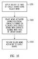
- FIG. 16is a flow chart of a method for surface mounting an actuator 100 , 400 , 700 , in accordance with an embodiment.
- Soldercan be applied to the pads (such as 1002 of FIG. 10 ) of the circuit board 200 , 500 , 800 using a solder mask, as indicated in block 1201 .
- the soldercan be applied to the contacts 104 , 404 , 704 of the actuator 100 , 400 , 700 .
- the actuator 100 , 400 , 700can be placed on the circuit board 200 , 500 , 800 , as indicated in block 1202 .
- the actuator 100 , 400 , 700can be unpackaged, e.g., not contained within a contemporary integrated circuit package such as a ball grid array package or a quad flat no-lead package.
- the actuator 100 , 400 , 700can be placed on the circuit board 200 , 500 , 800 with the contacts 104 , 404 , 704 of the actuator 100 , 400 , 700 aligned with the pads (such as 1002 of FIG. 10 ) of the circuit board 200 , 500 , 800 .
- the contactscan be formed upon flexures 1304 of the actuator 100 , 400 , 700 .
- the actuator 100 , 400 , 700can be placed on the circuit board 200 , 500 , 800 in various orientations, as indicated in block 1203 .
- the actuator 100can be placed on the circuit board 200 , 400 , 700 with the arm 101 extending upwardly, away from the circuit board 200 , as shown in FIGS. 2 and 3 .
- the actuator 100 , 400 , 700can be placed on the circuit board 200 , 500 , 800 in any desired orientation, including non-perpendicular orientations such as at 30°, 45°, and 60° (as measured between any desired feature of the actuator 100 , 400 , 700 and any desired feature of the circuit board 200 , 400 , 500 —such as a side thereof).
- the pads, such as pads 1003 of FIG. 10can be configured so as to accommodate a desired orientation.
- the actuator 400can be placed on the circuit board 500 with the arm 401 extending sideways, generally parallel to the circuit board 500 , as shown in FIGS. 5 and 6 .
- the actuator 700can be placed on the circuit board 800 with the arm 701 extending downwardly, away from the circuit board 800 , as shown in FIGS. 8 and 9 .
- a single actuatorcan have contacts formed up a plurality of surfaces thereof.
- the actuatorcan have one set of contacts formed upon the bottom thereof (as shown in FIG. 1 ), another set of contacts formed upon the side thereof (as shown in FIG. 4 ), and yet another set of contacts formed upon the top thereof (as shown in FIG. 7 , if the surface of the actuator 700 having the arm 701 extending therefrom is considered to be the top thereof, so as to be consistent with FIG. 1 ).
- the contactscan be redundant, such that any desired set can be used for surface mounting of the actuator. In this manner, a single actuator can be provided for use in a plurality of different orientations.
- the single actuatorcan be configured to be mounted to a circuit board in any one of a variety of different orientations.
- the actuatorcan be configured to be mounted to the circuit board with an arm thereof extending upwardly, extending sideways, or extending downwardly. That is, the actuator can have contacts formed upon any surface thereof.
- the arm 101 , 401 , 701can be considered to be an external part with respect to the actuator 100 , 400 , 700 .
- the arm 101 , 401 , 701moves with respect to the actuator 100 , 400 , 700 . Since the actuator 100 , 400 , 700 has an external moving part, contemporary packaging technologies, such as ball grid array (BGA) and quad flat no-lead (QFN) cannot be used with surface mount technology (SMT) to mount the actuator 100 , 400 , 700 because the packaging technology would interfere with desired movement of the arm 101 , 401 , 701 .
- BGAball grid array
- QFNquad flat no-lead
- SMTsurface mount technology
- the actuatorcan have a footprint of approximately 0.5 mm ⁇ 1.5 mm. This footprint is only slight larger than a standard 0402 surface mount component.
- the actuatoritself can define a package.
- features of the actuatorcan function as features of a package so as to facilitate mounting of the actuator.
- contacts formed upon flexures of the actuatorcan facilitate surface mounting of the actuator to a substrate.
- the actuatorcan be any type of MEMS actuator or non-MEMS actuator.
- MEMS actuatorsinclude comb drives, scratch drives, and thermal drives.
- non-MEMS actuatorsare voice coil actuators and piezoelectric actuators. The discussion of a MEMS actuator herein is by way of example only.
- surface mountingcan be defined to include various techniques of surface mounting technology (SMT). Examples of surface mounting techniques can include the use of flat contacts, leads, pins, and/or solder balls.
- the contactscan be formed of any conductor or semiconductor material.
- the contactscan be formed of metal to facilitate the use of solder to surface mount the actuator to a substrate.
- the contactscan be formed of aluminum nickel (Al/Ni) or titanium platinum nickel (Ti/Pt/Ni).
- the metallization of the substratecan be patterned such that the actuator rotates when the solder melts.
- the actuatorcan be placed in one direction (e.g. flat) upon the substrate and can end upon at 90° with respect to this direction (such that the actuator is standing upright when mounted).
- actuatorssuch as MEMS actuators
- surface mountingmore readily facilitates the mounting of actuators, such as MEMS actuators, in different orientations. Since the actuators can be more readily mounted in different orientations, the actuators can be used in a variety of applications.
- the flexurescan accommodate substantial mismatches in the coefficient of expansion between the actuator and the substrate upon which the actuator is mounted. Such flexures can also mitigate stress applied to the actuator due to shock, vibration, handling (such as by a person handling a mounted part and/or automated placement equipment, e.g., pick and place equipment).
- Each flexurecan have one electrical contact formed thereon.
- Each flexurecan have a plurality of electrical contacts formed thereon.
- One or more flexurescan have dummy contacts formed thereon. Each dummy contact can facilitate mechanical mounting of the actuator without providing any electrical connection thereto.
- Some contactscan be on flexures and some contacts can be without flexures. Any combination of contacts and flexures can be used.
Landscapes
- Engineering & Computer Science (AREA)
- Microelectronics & Electronic Packaging (AREA)
- Computer Hardware Design (AREA)
- Lens Barrels (AREA)
- Structures For Mounting Electric Components On Printed Circuit Boards (AREA)
Abstract
Description
Claims (30)
Priority Applications (3)
| Application Number | Priority Date | Filing Date | Title |
|---|---|---|---|
| US13/247,938US8571405B2 (en) | 2011-09-28 | 2011-09-28 | Surface mount actuator |
| PCT/US2012/058089WO2013049695A1 (en) | 2011-09-28 | 2012-09-28 | Surface mount mems actuator |
| US14/065,299US9414495B2 (en) | 2011-09-28 | 2013-10-28 | Surface mount actuator |
Applications Claiming Priority (1)
| Application Number | Priority Date | Filing Date | Title |
|---|---|---|---|
| US13/247,938US8571405B2 (en) | 2011-09-28 | 2011-09-28 | Surface mount actuator |
Related Child Applications (1)
| Application Number | Title | Priority Date | Filing Date |
|---|---|---|---|
| US14/065,299ContinuationUS9414495B2 (en) | 2011-09-28 | 2013-10-28 | Surface mount actuator |
Publications (2)
| Publication Number | Publication Date |
|---|---|
| US20130077948A1 US20130077948A1 (en) | 2013-03-28 |
| US8571405B2true US8571405B2 (en) | 2013-10-29 |
Family
ID=47080805
Family Applications (2)
| Application Number | Title | Priority Date | Filing Date |
|---|---|---|---|
| US13/247,938ActiveUS8571405B2 (en) | 2011-09-28 | 2011-09-28 | Surface mount actuator |
| US14/065,299ActiveUS9414495B2 (en) | 2011-09-28 | 2013-10-28 | Surface mount actuator |
Family Applications After (1)
| Application Number | Title | Priority Date | Filing Date |
|---|---|---|---|
| US14/065,299ActiveUS9414495B2 (en) | 2011-09-28 | 2013-10-28 | Surface mount actuator |
Country Status (2)
| Country | Link |
|---|---|
| US (2) | US8571405B2 (en) |
| WO (1) | WO2013049695A1 (en) |
Cited By (2)
| Publication number | Priority date | Publication date | Assignee | Title |
|---|---|---|---|---|
| US20140055971A1 (en)* | 2011-09-28 | 2014-02-27 | DigitalOptics Corporation MEMS | Surface mount actuator |
| US9817206B2 (en) | 2012-03-10 | 2017-11-14 | Digitaloptics Corporation | MEMS auto focus miniature camera module with fixed and movable lens groups |
Families Citing this family (2)
| Publication number | Priority date | Publication date | Assignee | Title |
|---|---|---|---|---|
| US7813634B2 (en)* | 2005-02-28 | 2010-10-12 | Tessera MEMS Technologies, Inc. | Autofocus camera |
| EP2934311B1 (en) | 2012-12-20 | 2020-04-15 | Volcano Corporation | Smooth transition catheters |
Citations (80)
| Publication number | Priority date | Publication date | Assignee | Title |
|---|---|---|---|---|
| US4333722A (en) | 1980-12-22 | 1982-06-08 | Eastman Kodak Company | Method of controlling electromagnetic actuator in a camera, and actuator controllable thereby |
| US4384778A (en) | 1981-11-09 | 1983-05-24 | Eastman Kodak Company | Integral, planar electromagnetic camera element/actuator |
| US4408857A (en) | 1982-03-22 | 1983-10-11 | Eastman Kodak Company | Method and circuit for controlling an electromagnetic actuator in photographic apparatus |
| US4496217A (en) | 1980-11-28 | 1985-01-29 | Canon Kabushiki Kaisha | Actuating device for photographic lens assembly |
| US4716432A (en) | 1986-04-24 | 1987-12-29 | Eastman Kodak Company | Exposure control apparatus |
| US4860040A (en) | 1987-06-19 | 1989-08-22 | Canon Kabushiki Kaisha | Camera |
| US5150260A (en) | 1990-10-02 | 1992-09-22 | Canon Kabushiki Kaisha | Optical apparatus |
| US5386294A (en) | 1990-07-05 | 1995-01-31 | Nikon Corporation | Pattern position measuring apparatus |
| US5699621A (en) | 1996-02-21 | 1997-12-23 | Massachusetts Institute Of Technology | Positioner with long travel in two dimensions |
| US5825560A (en) | 1995-02-28 | 1998-10-20 | Canon Kabushiki Xaisha | Optical apparatus |
| US5986826A (en) | 1996-12-17 | 1999-11-16 | Minolta Co., Ltd. | Drive device using electromechanical conversion element |
| US5995688A (en)* | 1998-06-01 | 1999-11-30 | Lucent Technologies, Inc. | Micro-opto-electromechanical devices and method therefor |
| US6033131A (en) | 1998-09-30 | 2000-03-07 | Eastman Kodak Company | Hybrid silicon-based micro-electromagnetic light shutter |
| US6068801A (en) | 1996-12-19 | 2000-05-30 | Telefonaktiebolaget Lm Ericsson | Method for making elastic bumps from a wafer mold having grooves |
| US6205267B1 (en) | 1998-11-20 | 2001-03-20 | Lucent Technologies | Optical switch |
| US20010004420A1 (en) | 1999-12-17 | 2001-06-21 | Minolta Co., Ltd. | Driving system with elastically supporting units |
| US6262827B1 (en) | 1999-06-29 | 2001-07-17 | Fujitsu Limited | Galvano-mirror |
| US20020006687A1 (en) | 2000-05-23 | 2002-01-17 | Lam Ken M. | Integrated IC chip package for electronic image sensor die |
| US6392703B1 (en) | 1995-02-28 | 2002-05-21 | Canon Kabushiki Kaisha | Optical apparatus for forming an object image on a sensing element |
| US20020070634A1 (en) | 2000-09-25 | 2002-06-13 | Yu-Chong Tai | Freestanding polymer MEMS structures with anti stiction |
| US6426777B1 (en) | 1997-04-03 | 2002-07-30 | Asahi Kogaku Kogyo Kabushiki Kaisha | Hybrid camera selectively using either silver-halide-type photographic film or photoelectric-conversion-type image sensor |
| US20020105699A1 (en) | 2001-02-02 | 2002-08-08 | Teravicta Technologies, Inc | Integrated optical micro-electromechanical systems and methods of fabricating and operating the same |
| US20020125789A1 (en) | 2001-03-07 | 2002-09-12 | Jobst Brandt | Micro-mover with balanced dynamics |
| US6497141B1 (en) | 1999-06-07 | 2002-12-24 | Cornell Research Foundation Inc. | Parametric resonance in microelectromechanical structures |
| US20030048036A1 (en) | 2001-08-31 | 2003-03-13 | Lemkin Mark Alan | MEMS comb-finger actuator |
| US6535311B1 (en) | 1999-12-09 | 2003-03-18 | Corning Incorporated | Wavelength selective cross-connect switch using a MEMS shutter array |
| US20030062422A1 (en) | 2001-09-10 | 2003-04-03 | Fateley William G. | System and method for encoded spatio-spectral information processing |
| US20030076421A1 (en) | 2001-10-19 | 2003-04-24 | Nokia Corporation | Image stabilizer for a microcamera module of a handheld device, and method for stabilizing a microcamera module of a handheld device |
| US20030086751A1 (en) | 2001-11-08 | 2003-05-08 | Culpepper Martin L | Multiple degree of freedom compliant mechanism |
| US20030210116A1 (en)* | 2002-05-08 | 2003-11-13 | Motorola, Inc. | Micro electro-mechanical system with one or more moving parts method and apparatus |
| US6674383B2 (en) | 2000-11-01 | 2004-01-06 | Onix Microsystems, Inc. | PWM-based measurement interface for a micro-machined electrostatic actuator |
| US6675671B1 (en) | 2002-05-22 | 2004-01-13 | Sandia Corporation | Planar-constructed spatial micro-stage |
| US20040048410A1 (en) | 2002-09-09 | 2004-03-11 | Motorola Inc. | SOI polysilicon trench refill perimeter oxide anchor scheme |
| US20040066494A1 (en) | 2002-08-30 | 2004-04-08 | Samsung Electronics, Co., Ltd. | Highly efficient scrolling projection system and method |
| US20040183936A1 (en) | 2003-03-18 | 2004-09-23 | Young-Jun Kim | Digital camera module, apparatus and method of assembling the same |
| US20040189969A1 (en) | 2003-03-14 | 2004-09-30 | Makoto Mizuno | Drive mechanism, exposure device, optical equipment, and device manufacturing method |
| US20040201773A1 (en) | 2001-02-08 | 2004-10-14 | Toni Ostergard | Microminiature zoom system for digital camera |
| US20050002086A1 (en) | 2000-10-31 | 2005-01-06 | Microsoft Corporation | Microelectrical mechanical structure (MEMS) optical modulator and optical display system |
| US20050002008A1 (en) | 2003-05-06 | 2005-01-06 | Asml Netherlands B.V. | Lithographic apparatus, device manufacturing method and device manufactured thereby |
| US20050007489A1 (en) | 2003-07-08 | 2005-01-13 | Lg Electronics Inc. | Rotary camera assembly of mobile communication device |
| US6847907B1 (en) | 2002-12-31 | 2005-01-25 | Active Optical Networks, Inc. | Defect detection and repair of micro-electro-mechanical systems (MEMS) devices |
| US6850675B1 (en) | 2002-02-04 | 2005-02-01 | Siwave, Inc. | Base, payload and connecting structure and methods of making the same |
| US20050095813A1 (en) | 2003-11-05 | 2005-05-05 | Xu Zhu | Ultrathin form factor MEMS microphones and microspeakers |
| US20050139542A1 (en) | 2001-10-22 | 2005-06-30 | Dickensheets David L. | Stiffened surface micromachined structures and process for fabricating the same |
| US20050148433A1 (en) | 2003-12-31 | 2005-07-07 | Shen-Tai Industry Co., Ltd. | Water trampoline |
| US20050219399A1 (en) | 2004-03-30 | 2005-10-06 | Fuji Photo Film Co., Ltd | Image capture apparatus |
| US6958777B1 (en) | 2000-09-29 | 2005-10-25 | Ess Technology, Inc. | Exposure control in electromechanical imaging devices |
| US20050249487A1 (en) | 2004-03-12 | 2005-11-10 | Gutierrez Roman C | Miniature camera |
| US20060028320A1 (en) | 2004-08-09 | 2006-02-09 | Mitsumi Electric Co., Ltd. | Autofocus actuator |
| US20060033938A1 (en) | 2004-08-12 | 2006-02-16 | Kopf Dale R | Image-forming apparatus |
| US7027206B2 (en) | 2004-01-26 | 2006-04-11 | Fuji Photo Film Co., Ltd. | Spatial light modulator, spatial light modulator array, and image formation apparatus |
| US7038150B1 (en) | 2004-07-06 | 2006-05-02 | Sandia Corporation | Micro environmental sensing device |
| US20060183332A1 (en) | 2005-02-14 | 2006-08-17 | Samsung Electronics Co., Ltd. | Method of manufacturing floating structure |
| US20060193618A1 (en) | 2005-02-28 | 2006-08-31 | Calvet Robert J | Axial snubbers for camera |
| US20060192858A1 (en) | 2005-02-28 | 2006-08-31 | Calvet Robert J | Oil damping for camera optical assembly |
| US20060204242A1 (en) | 2005-02-28 | 2006-09-14 | Gutierrez Roman C | Autofocus camera |
| US20060209012A1 (en) | 2005-02-23 | 2006-09-21 | Pixtronix, Incorporated | Devices having MEMS displays |
| US20060219006A1 (en) | 2003-10-20 | 2006-10-05 | Nasiri Steven S | Method of making an X-Y axis dual-mass tuning fork gyroscope with vertically integrated electronics and wafer-scale hermetic packaging |
| US20060250325A1 (en) | 2005-02-23 | 2006-11-09 | Pixtronix, Incorporated | Display methods and apparatus |
| US7154199B2 (en) | 2004-12-24 | 2006-12-26 | Canon Kabushiki Kaisha | Driving apparatus for moving member to be moved |
| US20070133976A1 (en) | 2005-02-28 | 2007-06-14 | Gutierrez Roman C | Shutter for miniature camera |
| US20080020573A1 (en) | 2004-10-21 | 2008-01-24 | Jeffrey Birkmeyer | Sacrificial substrate for etching |
| US20080044172A1 (en) | 2005-02-28 | 2008-02-21 | Tang Tony K | Lens barrel assembly |
| US20080075309A1 (en) | 2006-09-08 | 2008-03-27 | Industrial Technology Research Institute | Structure and manufacturing method of inversed microphone chip component |
| US7372074B2 (en) | 2005-10-11 | 2008-05-13 | Honeywell International, Inc. | Surface preparation for selective silicon fusion bonding |
| US7436207B2 (en)* | 2006-07-21 | 2008-10-14 | Microchip Technology Incorporated | Integrated circuit device having at least one of a plurality of bond pads with a selectable plurality of input-output functionalities |
| US7545591B1 (en) | 2006-10-17 | 2009-06-09 | Siimpel Corporation | Uniform wall thickness lens barrel |
| US7579848B2 (en)* | 2000-05-23 | 2009-08-25 | Nanonexus, Inc. | High density interconnect system for IC packages and interconnect assemblies |
| US7646969B2 (en) | 2005-02-28 | 2010-01-12 | Siimpel Corporation | Camera snubber assembly |
| US7705909B2 (en) | 2006-08-31 | 2010-04-27 | Mitsumi Electric Co., Ltd. | Camera module with improved leaf spring attachment |
| US7720366B2 (en) | 2006-05-08 | 2010-05-18 | Tamron Co., Ltd | Actuator, and lens unit and camera with the same |
| US20100232777A1 (en) | 2009-03-13 | 2010-09-16 | Largan Precision Co., Ltd. | Photographing module |
| US20100284081A1 (en) | 2009-05-08 | 2010-11-11 | Gutierrez Roman C | Integrated lens barrel |
| US7838322B1 (en) | 2005-02-28 | 2010-11-23 | Tessera MEMS Technologies, Inc. | Method of enhancing an etch system |
| WO2010138931A2 (en) | 2009-05-29 | 2010-12-02 | Siimpel Corporation | Mechanical isolation for mems electrical contacts |
| US7855489B2 (en)* | 2007-01-31 | 2010-12-21 | Hitachi Global Storage Technologies, Netherlands, B.V. | Microactuator substrate |
| US20110026148A1 (en) | 2008-04-08 | 2011-02-03 | Konica Minolta Holdings, Inc. | Actuator array sheet |
| US7990628B1 (en) | 2007-08-29 | 2011-08-02 | Tessera MEMS Technologies, Inc. | Planar flexure system with high pitch stiffness |
| US8178936B2 (en)* | 2008-02-28 | 2012-05-15 | Shandong Gettop Acoustic Co. Ltd. | Double-side mountable MEMS package |
| US8299598B2 (en)* | 1995-12-19 | 2012-10-30 | Round Rock Research, Llc | Grid array packages and assemblies including the same |
Family Cites Families (3)
| Publication number | Priority date | Publication date | Assignee | Title |
|---|---|---|---|---|
| WO2008070673A2 (en)* | 2006-12-04 | 2008-06-12 | Nanonexus, Inc. | Construction structures and manufacturing processes for integrated circuit wafer probe card assemblies |
| US8243397B2 (en)* | 2007-06-20 | 2012-08-14 | Carnegie Mellon University | Micromachined electrothermal rotary actuator |
| US8571405B2 (en)* | 2011-09-28 | 2013-10-29 | DigitalOptics Corporation MEMS | Surface mount actuator |
- 2011
- 2011-09-28USUS13/247,938patent/US8571405B2/enactiveActive
- 2012
- 2012-09-28WOPCT/US2012/058089patent/WO2013049695A1/enactiveApplication Filing
- 2013
- 2013-10-28USUS14/065,299patent/US9414495B2/enactiveActive
Patent Citations (87)
| Publication number | Priority date | Publication date | Assignee | Title |
|---|---|---|---|---|
| US4496217A (en) | 1980-11-28 | 1985-01-29 | Canon Kabushiki Kaisha | Actuating device for photographic lens assembly |
| US4333722A (en) | 1980-12-22 | 1982-06-08 | Eastman Kodak Company | Method of controlling electromagnetic actuator in a camera, and actuator controllable thereby |
| US4384778A (en) | 1981-11-09 | 1983-05-24 | Eastman Kodak Company | Integral, planar electromagnetic camera element/actuator |
| US4408857A (en) | 1982-03-22 | 1983-10-11 | Eastman Kodak Company | Method and circuit for controlling an electromagnetic actuator in photographic apparatus |
| US4716432A (en) | 1986-04-24 | 1987-12-29 | Eastman Kodak Company | Exposure control apparatus |
| US4860040A (en) | 1987-06-19 | 1989-08-22 | Canon Kabushiki Kaisha | Camera |
| US5386294A (en) | 1990-07-05 | 1995-01-31 | Nikon Corporation | Pattern position measuring apparatus |
| US5150260A (en) | 1990-10-02 | 1992-09-22 | Canon Kabushiki Kaisha | Optical apparatus |
| US6392703B1 (en) | 1995-02-28 | 2002-05-21 | Canon Kabushiki Kaisha | Optical apparatus for forming an object image on a sensing element |
| US5825560A (en) | 1995-02-28 | 1998-10-20 | Canon Kabushiki Xaisha | Optical apparatus |
| US8299598B2 (en)* | 1995-12-19 | 2012-10-30 | Round Rock Research, Llc | Grid array packages and assemblies including the same |
| US5699621A (en) | 1996-02-21 | 1997-12-23 | Massachusetts Institute Of Technology | Positioner with long travel in two dimensions |
| US5986826A (en) | 1996-12-17 | 1999-11-16 | Minolta Co., Ltd. | Drive device using electromechanical conversion element |
| US6068801A (en) | 1996-12-19 | 2000-05-30 | Telefonaktiebolaget Lm Ericsson | Method for making elastic bumps from a wafer mold having grooves |
| US6426777B1 (en) | 1997-04-03 | 2002-07-30 | Asahi Kogaku Kogyo Kabushiki Kaisha | Hybrid camera selectively using either silver-halide-type photographic film or photoelectric-conversion-type image sensor |
| US5995688A (en)* | 1998-06-01 | 1999-11-30 | Lucent Technologies, Inc. | Micro-opto-electromechanical devices and method therefor |
| US6033131A (en) | 1998-09-30 | 2000-03-07 | Eastman Kodak Company | Hybrid silicon-based micro-electromagnetic light shutter |
| US6205267B1 (en) | 1998-11-20 | 2001-03-20 | Lucent Technologies | Optical switch |
| US6497141B1 (en) | 1999-06-07 | 2002-12-24 | Cornell Research Foundation Inc. | Parametric resonance in microelectromechanical structures |
| US6262827B1 (en) | 1999-06-29 | 2001-07-17 | Fujitsu Limited | Galvano-mirror |
| US6535311B1 (en) | 1999-12-09 | 2003-03-18 | Corning Incorporated | Wavelength selective cross-connect switch using a MEMS shutter array |
| US20010004420A1 (en) | 1999-12-17 | 2001-06-21 | Minolta Co., Ltd. | Driving system with elastically supporting units |
| US20020006687A1 (en) | 2000-05-23 | 2002-01-17 | Lam Ken M. | Integrated IC chip package for electronic image sensor die |
| US7579848B2 (en)* | 2000-05-23 | 2009-08-25 | Nanonexus, Inc. | High density interconnect system for IC packages and interconnect assemblies |
| US20020070634A1 (en) | 2000-09-25 | 2002-06-13 | Yu-Chong Tai | Freestanding polymer MEMS structures with anti stiction |
| US6958777B1 (en) | 2000-09-29 | 2005-10-25 | Ess Technology, Inc. | Exposure control in electromechanical imaging devices |
| US20050002086A1 (en) | 2000-10-31 | 2005-01-06 | Microsoft Corporation | Microelectrical mechanical structure (MEMS) optical modulator and optical display system |
| US6674383B2 (en) | 2000-11-01 | 2004-01-06 | Onix Microsystems, Inc. | PWM-based measurement interface for a micro-machined electrostatic actuator |
| US20020105699A1 (en) | 2001-02-02 | 2002-08-08 | Teravicta Technologies, Inc | Integrated optical micro-electromechanical systems and methods of fabricating and operating the same |
| US20040201773A1 (en) | 2001-02-08 | 2004-10-14 | Toni Ostergard | Microminiature zoom system for digital camera |
| US6914635B2 (en) | 2001-02-08 | 2005-07-05 | Nokia Mobile Phones, Ltd. | Microminiature zoom system for digital camera |
| US20020125789A1 (en) | 2001-03-07 | 2002-09-12 | Jobst Brandt | Micro-mover with balanced dynamics |
| US20030048036A1 (en) | 2001-08-31 | 2003-03-13 | Lemkin Mark Alan | MEMS comb-finger actuator |
| US20030062422A1 (en) | 2001-09-10 | 2003-04-03 | Fateley William G. | System and method for encoded spatio-spectral information processing |
| US20030076421A1 (en) | 2001-10-19 | 2003-04-24 | Nokia Corporation | Image stabilizer for a microcamera module of a handheld device, and method for stabilizing a microcamera module of a handheld device |
| US20050139542A1 (en) | 2001-10-22 | 2005-06-30 | Dickensheets David L. | Stiffened surface micromachined structures and process for fabricating the same |
| US20030086751A1 (en) | 2001-11-08 | 2003-05-08 | Culpepper Martin L | Multiple degree of freedom compliant mechanism |
| US6850675B1 (en) | 2002-02-04 | 2005-02-01 | Siwave, Inc. | Base, payload and connecting structure and methods of making the same |
| US7113688B2 (en) | 2002-02-04 | 2006-09-26 | Siimpel Corporation | Base, payload and connecting structure and methods of making the same |
| US7266272B1 (en) | 2002-02-04 | 2007-09-04 | Siimpel Corporation | Motion control stages and methods of making the same |
| US20030210116A1 (en)* | 2002-05-08 | 2003-11-13 | Motorola, Inc. | Micro electro-mechanical system with one or more moving parts method and apparatus |
| US6675671B1 (en) | 2002-05-22 | 2004-01-13 | Sandia Corporation | Planar-constructed spatial micro-stage |
| US20040066494A1 (en) | 2002-08-30 | 2004-04-08 | Samsung Electronics, Co., Ltd. | Highly efficient scrolling projection system and method |
| US20040048410A1 (en) | 2002-09-09 | 2004-03-11 | Motorola Inc. | SOI polysilicon trench refill perimeter oxide anchor scheme |
| US6847907B1 (en) | 2002-12-31 | 2005-01-25 | Active Optical Networks, Inc. | Defect detection and repair of micro-electro-mechanical systems (MEMS) devices |
| US20040189969A1 (en) | 2003-03-14 | 2004-09-30 | Makoto Mizuno | Drive mechanism, exposure device, optical equipment, and device manufacturing method |
| US20040183936A1 (en) | 2003-03-18 | 2004-09-23 | Young-Jun Kim | Digital camera module, apparatus and method of assembling the same |
| US20050002008A1 (en) | 2003-05-06 | 2005-01-06 | Asml Netherlands B.V. | Lithographic apparatus, device manufacturing method and device manufactured thereby |
| US20050007489A1 (en) | 2003-07-08 | 2005-01-13 | Lg Electronics Inc. | Rotary camera assembly of mobile communication device |
| US20060219006A1 (en) | 2003-10-20 | 2006-10-05 | Nasiri Steven S | Method of making an X-Y axis dual-mass tuning fork gyroscope with vertically integrated electronics and wafer-scale hermetic packaging |
| US20050095813A1 (en) | 2003-11-05 | 2005-05-05 | Xu Zhu | Ultrathin form factor MEMS microphones and microspeakers |
| US20050148433A1 (en) | 2003-12-31 | 2005-07-07 | Shen-Tai Industry Co., Ltd. | Water trampoline |
| US7027206B2 (en) | 2004-01-26 | 2006-04-11 | Fuji Photo Film Co., Ltd. | Spatial light modulator, spatial light modulator array, and image formation apparatus |
| US7477842B2 (en)* | 2004-03-12 | 2009-01-13 | Siimpel, Inc. | Miniature camera |
| US20050249487A1 (en) | 2004-03-12 | 2005-11-10 | Gutierrez Roman C | Miniature camera |
| US20050219399A1 (en) | 2004-03-30 | 2005-10-06 | Fuji Photo Film Co., Ltd | Image capture apparatus |
| US7038150B1 (en) | 2004-07-06 | 2006-05-02 | Sandia Corporation | Micro environmental sensing device |
| US20060028320A1 (en) | 2004-08-09 | 2006-02-09 | Mitsumi Electric Co., Ltd. | Autofocus actuator |
| US7285879B2 (en) | 2004-08-09 | 2007-10-23 | Mitsumi Electric Co., Ltd. | Autofocus actuator |
| US20060033938A1 (en) | 2004-08-12 | 2006-02-16 | Kopf Dale R | Image-forming apparatus |
| US20080020573A1 (en) | 2004-10-21 | 2008-01-24 | Jeffrey Birkmeyer | Sacrificial substrate for etching |
| US7154199B2 (en) | 2004-12-24 | 2006-12-26 | Canon Kabushiki Kaisha | Driving apparatus for moving member to be moved |
| US20060183332A1 (en) | 2005-02-14 | 2006-08-17 | Samsung Electronics Co., Ltd. | Method of manufacturing floating structure |
| US20060209012A1 (en) | 2005-02-23 | 2006-09-21 | Pixtronix, Incorporated | Devices having MEMS displays |
| US20060250325A1 (en) | 2005-02-23 | 2006-11-09 | Pixtronix, Incorporated | Display methods and apparatus |
| US20070133976A1 (en) | 2005-02-28 | 2007-06-14 | Gutierrez Roman C | Shutter for miniature camera |
| US7838322B1 (en) | 2005-02-28 | 2010-11-23 | Tessera MEMS Technologies, Inc. | Method of enhancing an etch system |
| US20060204242A1 (en) | 2005-02-28 | 2006-09-14 | Gutierrez Roman C | Autofocus camera |
| US20080044172A1 (en) | 2005-02-28 | 2008-02-21 | Tang Tony K | Lens barrel assembly |
| US7555210B2 (en) | 2005-02-28 | 2009-06-30 | Siimpel, Inc. | Axial snubbers for camera |
| US20060192858A1 (en) | 2005-02-28 | 2006-08-31 | Calvet Robert J | Oil damping for camera optical assembly |
| US7646969B2 (en) | 2005-02-28 | 2010-01-12 | Siimpel Corporation | Camera snubber assembly |
| US20060193618A1 (en) | 2005-02-28 | 2006-08-31 | Calvet Robert J | Axial snubbers for camera |
| US7372074B2 (en) | 2005-10-11 | 2008-05-13 | Honeywell International, Inc. | Surface preparation for selective silicon fusion bonding |
| US7720366B2 (en) | 2006-05-08 | 2010-05-18 | Tamron Co., Ltd | Actuator, and lens unit and camera with the same |
| US7436207B2 (en)* | 2006-07-21 | 2008-10-14 | Microchip Technology Incorporated | Integrated circuit device having at least one of a plurality of bond pads with a selectable plurality of input-output functionalities |
| US7705909B2 (en) | 2006-08-31 | 2010-04-27 | Mitsumi Electric Co., Ltd. | Camera module with improved leaf spring attachment |
| US20080075309A1 (en) | 2006-09-08 | 2008-03-27 | Industrial Technology Research Institute | Structure and manufacturing method of inversed microphone chip component |
| US7545591B1 (en) | 2006-10-17 | 2009-06-09 | Siimpel Corporation | Uniform wall thickness lens barrel |
| US7855489B2 (en)* | 2007-01-31 | 2010-12-21 | Hitachi Global Storage Technologies, Netherlands, B.V. | Microactuator substrate |
| US7990628B1 (en) | 2007-08-29 | 2011-08-02 | Tessera MEMS Technologies, Inc. | Planar flexure system with high pitch stiffness |
| US8178936B2 (en)* | 2008-02-28 | 2012-05-15 | Shandong Gettop Acoustic Co. Ltd. | Double-side mountable MEMS package |
| US20110026148A1 (en) | 2008-04-08 | 2011-02-03 | Konica Minolta Holdings, Inc. | Actuator array sheet |
| US20100232777A1 (en) | 2009-03-13 | 2010-09-16 | Largan Precision Co., Ltd. | Photographing module |
| US20100284081A1 (en) | 2009-05-08 | 2010-11-11 | Gutierrez Roman C | Integrated lens barrel |
| US8004780B2 (en)* | 2009-05-08 | 2011-08-23 | Tessera MEMS Technologies, Inc. | Integrated lens barrel |
| WO2010138931A2 (en) | 2009-05-29 | 2010-12-02 | Siimpel Corporation | Mechanical isolation for mems electrical contacts |
Non-Patent Citations (7)
| Title |
|---|
| Akihiro Koga et al. "Electrostatic Linear Microactuator Mechanism for Focusing a CCD Camera"; Journal of Lightwave Technology, vol. 17, No. 1: p. 43-47; Jan. 1999. |
| Chapter 2: Electrical Microactuators, Apr. 11, 2005. |
| Fernandez, Daniel, et al., Pulse-Drive and Capacitive Measurement Circuit for MEMS Electrostatic Actuators, Stresa, Italy, Apr. 25-27, 2007. |
| Improving Test Efficiency of MEMS Electrostatic Actuators Using the Agilent E4980A Precision LCR Meter, Agilent Technologies, Inc., Apr. 12, 2007. |
| Measuring Capacitance: Methods (fwd); Apr. 26, 1998 http://www.pupman.com/listarchives/1998/April/msg00625.html. |
| PCT/US 06/07024 Search Report of Nov. 28, 2007. |
| Polymems Actuator: A Polymer-Based Microelectromechanical (MEMS) Actuator with Macroscopic Action, Honeywell International Incorporated, Final Technical Report, Sep. 2002. |
Cited By (3)
| Publication number | Priority date | Publication date | Assignee | Title |
|---|---|---|---|---|
| US20140055971A1 (en)* | 2011-09-28 | 2014-02-27 | DigitalOptics Corporation MEMS | Surface mount actuator |
| US9414495B2 (en)* | 2011-09-28 | 2016-08-09 | DigitalOptics Corporation MEMS | Surface mount actuator |
| US9817206B2 (en) | 2012-03-10 | 2017-11-14 | Digitaloptics Corporation | MEMS auto focus miniature camera module with fixed and movable lens groups |
Also Published As
| Publication number | Publication date |
|---|---|
| US20140055971A1 (en) | 2014-02-27 |
| WO2013049695A1 (en) | 2013-04-04 |
| US20130077948A1 (en) | 2013-03-28 |
| US9414495B2 (en) | 2016-08-09 |
Similar Documents
| Publication | Publication Date | Title |
|---|---|---|
| TWI528809B (en) | Integrated substrate for anti-shake apparatus | |
| US9578217B2 (en) | Moving image sensor package | |
| US8606057B1 (en) | Opto-electronic modules including electrically conductive connections for integration with an electronic device | |
| KR102003043B1 (en) | Flexible printed circuit board and small camera apparatus having the same | |
| US8665364B2 (en) | Reinforcement structure for wafer-level camera module | |
| CN202841335U (en) | Integrated substrate structure for preventing hand vibration | |
| JP5919440B2 (en) | Imaging module and electronic device | |
| US9414495B2 (en) | Surface mount actuator | |
| US9712732B2 (en) | Imaging module, electronic device provided therewith, and imaging-module manufacturing method | |
| KR20200097086A (en) | Package board for image sensor and camera module including the same | |
| JP5913284B2 (en) | Device with optical module and support plate | |
| CN111580236B (en) | Motor lens assembly and corresponding camera module | |
| EP4216535B1 (en) | Camera module and electronic device | |
| KR20150007672A (en) | Camera Module | |
| JP2012070102A (en) | Imaging apparatus and manufacturing method thereof | |
| JP2009296454A (en) | Camera module and mobile terminal | |
| JP2008192818A (en) | Microball mounting device and mounting method thereof | |
| KR100619329B1 (en) | Embedded IC packaging structure | |
| US20100221860A1 (en) | Precision micro-electromechanical sensor (mems) mounting in organic packaging | |
| CN111164957B (en) | Substrate stack and imaging device | |
| US11309235B2 (en) | Semiconductor module, electronic device, and printed wiring board | |
| JP2009210324A (en) | Acceleration switch | |
| KR20230000350A (en) | A camera module and optical apparatus having the same | |
| KR101075688B1 (en) | Optical image stabilization device and manufacturing method thereof | |
| JP2012134397A (en) | Optical device module |
Legal Events
| Date | Code | Title | Description |
|---|---|---|---|
| AS | Assignment | Owner name:DIGITALOPTICS CORPORATION MEMS, CALIFORNIA Free format text:ASSIGNMENT OF ASSIGNORS INTEREST;ASSIGNOR:GUTIERREZ, ROMAN C.;REEL/FRAME:026986/0240 Effective date:20110922 | |
| STCF | Information on status: patent grant | Free format text:PATENTED CASE | |
| FEPP | Fee payment procedure | Free format text:PAYOR NUMBER ASSIGNED (ORIGINAL EVENT CODE: ASPN); ENTITY STATUS OF PATENT OWNER: LARGE ENTITY | |
| AS | Assignment | Owner name:ROYAL BANK OF CANADA, AS COLLATERAL AGENT, CANADA Free format text:SECURITY INTEREST;ASSIGNORS:INVENSAS CORPORATION;TESSERA, INC.;TESSERA ADVANCED TECHNOLOGIES, INC.;AND OTHERS;REEL/FRAME:040797/0001 Effective date:20161201 | |
| FPAY | Fee payment | Year of fee payment:4 | |
| AS | Assignment | Owner name:PHORUS, INC., CALIFORNIA Free format text:RELEASE BY SECURED PARTY;ASSIGNOR:ROYAL BANK OF CANADA;REEL/FRAME:052920/0001 Effective date:20200601 Owner name:FOTONATION CORPORATION (F/K/A DIGITALOPTICS CORPORATION AND F/K/A DIGITALOPTICS CORPORATION MEMS), CALIFORNIA Free format text:RELEASE BY SECURED PARTY;ASSIGNOR:ROYAL BANK OF CANADA;REEL/FRAME:052920/0001 Effective date:20200601 Owner name:INVENSAS CORPORATION, CALIFORNIA Free format text:RELEASE BY SECURED PARTY;ASSIGNOR:ROYAL BANK OF CANADA;REEL/FRAME:052920/0001 Effective date:20200601 Owner name:DTS LLC, CALIFORNIA Free format text:RELEASE BY SECURED PARTY;ASSIGNOR:ROYAL BANK OF CANADA;REEL/FRAME:052920/0001 Effective date:20200601 Owner name:DTS, INC., CALIFORNIA Free format text:RELEASE BY SECURED PARTY;ASSIGNOR:ROYAL BANK OF CANADA;REEL/FRAME:052920/0001 Effective date:20200601 Owner name:IBIQUITY DIGITAL CORPORATION, MARYLAND Free format text:RELEASE BY SECURED PARTY;ASSIGNOR:ROYAL BANK OF CANADA;REEL/FRAME:052920/0001 Effective date:20200601 Owner name:TESSERA ADVANCED TECHNOLOGIES, INC, CALIFORNIA Free format text:RELEASE BY SECURED PARTY;ASSIGNOR:ROYAL BANK OF CANADA;REEL/FRAME:052920/0001 Effective date:20200601 Owner name:TESSERA, INC., CALIFORNIA Free format text:RELEASE BY SECURED PARTY;ASSIGNOR:ROYAL BANK OF CANADA;REEL/FRAME:052920/0001 Effective date:20200601 Owner name:INVENSAS BONDING TECHNOLOGIES, INC. (F/K/A ZIPTRONIX, INC.), CALIFORNIA Free format text:RELEASE BY SECURED PARTY;ASSIGNOR:ROYAL BANK OF CANADA;REEL/FRAME:052920/0001 Effective date:20200601 | |
| MAFP | Maintenance fee payment | Free format text:PAYMENT OF MAINTENANCE FEE, 8TH YEAR, LARGE ENTITY (ORIGINAL EVENT CODE: M1552); ENTITY STATUS OF PATENT OWNER: LARGE ENTITY Year of fee payment:8 | |
| AS | Assignment | Owner name:BANK OF AMERICA, N.A., AS COLLATERAL AGENT, NORTH CAROLINA Free format text:SECURITY INTEREST;ASSIGNORS:ADEIA GUIDES INC.;ADEIA IMAGING LLC;ADEIA MEDIA HOLDINGS LLC;AND OTHERS;REEL/FRAME:063529/0272 Effective date:20230501 | |
| MAFP | Maintenance fee payment | Free format text:PAYMENT OF MAINTENANCE FEE, 12TH YEAR, LARGE ENTITY (ORIGINAL EVENT CODE: M1553); ENTITY STATUS OF PATENT OWNER: LARGE ENTITY Year of fee payment:12 |