US8570803B2 - Semiconductor memory having both volatile and non-volatile functionality and method of operating - Google Patents
Semiconductor memory having both volatile and non-volatile functionality and method of operatingDownload PDFInfo
- Publication number
- US8570803B2 US8570803B2US13/758,646US201313758646AUS8570803B2US 8570803 B2US8570803 B2US 8570803B2US 201313758646 AUS201313758646 AUS 201313758646AUS 8570803 B2US8570803 B2US 8570803B2
- Authority
- US
- United States
- Prior art keywords
- trapping layer
- memory cell
- floating body
- terminal
- floating
- Prior art date
- Legal status (The legal status is an assumption and is not a legal conclusion. Google has not performed a legal analysis and makes no representation as to the accuracy of the status listed.)
- Active
Links
Images


Classifications
- H—ELECTRICITY
- H10—SEMICONDUCTOR DEVICES; ELECTRIC SOLID-STATE DEVICES NOT OTHERWISE PROVIDED FOR
- H10B—ELECTRONIC MEMORY DEVICES
- H10B12/00—Dynamic random access memory [DRAM] devices
- H10B12/20—DRAM devices comprising floating-body transistors, e.g. floating-body cells
- G—PHYSICS
- G11—INFORMATION STORAGE
- G11C—STATIC STORES
- G11C11/00—Digital stores characterised by the use of particular electric or magnetic storage elements; Storage elements therefor
- G11C11/21—Digital stores characterised by the use of particular electric or magnetic storage elements; Storage elements therefor using electric elements
- G11C11/34—Digital stores characterised by the use of particular electric or magnetic storage elements; Storage elements therefor using electric elements using semiconductor devices
- G11C11/40—Digital stores characterised by the use of particular electric or magnetic storage elements; Storage elements therefor using electric elements using semiconductor devices using transistors
- G11C11/401—Digital stores characterised by the use of particular electric or magnetic storage elements; Storage elements therefor using electric elements using semiconductor devices using transistors forming cells needing refreshing or charge regeneration, i.e. dynamic cells
- G11C11/403—Digital stores characterised by the use of particular electric or magnetic storage elements; Storage elements therefor using electric elements using semiconductor devices using transistors forming cells needing refreshing or charge regeneration, i.e. dynamic cells with charge regeneration common to a multiplicity of memory cells, i.e. external refresh
- G11C11/404—Digital stores characterised by the use of particular electric or magnetic storage elements; Storage elements therefor using electric elements using semiconductor devices using transistors forming cells needing refreshing or charge regeneration, i.e. dynamic cells with charge regeneration common to a multiplicity of memory cells, i.e. external refresh with one charge-transfer gate, e.g. MOS transistor, per cell
- G—PHYSICS
- G11—INFORMATION STORAGE
- G11C—STATIC STORES
- G11C11/00—Digital stores characterised by the use of particular electric or magnetic storage elements; Storage elements therefor
- G11C11/21—Digital stores characterised by the use of particular electric or magnetic storage elements; Storage elements therefor using electric elements
- G11C11/34—Digital stores characterised by the use of particular electric or magnetic storage elements; Storage elements therefor using electric elements using semiconductor devices
- G11C11/40—Digital stores characterised by the use of particular electric or magnetic storage elements; Storage elements therefor using electric elements using semiconductor devices using transistors
- G—PHYSICS
- G11—INFORMATION STORAGE
- G11C—STATIC STORES
- G11C14/00—Digital stores characterised by arrangements of cells having volatile and non-volatile storage properties for back-up when the power is down
- G11C14/0009—Digital stores characterised by arrangements of cells having volatile and non-volatile storage properties for back-up when the power is down in which the volatile element is a DRAM cell
- G11C14/0018—Digital stores characterised by arrangements of cells having volatile and non-volatile storage properties for back-up when the power is down in which the volatile element is a DRAM cell whereby the nonvolatile element is an EEPROM element, e.g. a floating gate or metal-nitride-oxide-silicon [MNOS] transistor
- H—ELECTRICITY
- H10—SEMICONDUCTOR DEVICES; ELECTRIC SOLID-STATE DEVICES NOT OTHERWISE PROVIDED FOR
- H10D—INORGANIC ELECTRIC SEMICONDUCTOR DEVICES
- H10D30/00—Field-effect transistors [FET]
- H10D30/01—Manufacture or treatment
- H10D30/021—Manufacture or treatment of FETs having insulated gates [IGFET]
- H10D30/0411—Manufacture or treatment of FETs having insulated gates [IGFET] of FETs having floating gates
- H—ELECTRICITY
- H10—SEMICONDUCTOR DEVICES; ELECTRIC SOLID-STATE DEVICES NOT OTHERWISE PROVIDED FOR
- H10D—INORGANIC ELECTRIC SEMICONDUCTOR DEVICES
- H10D30/00—Field-effect transistors [FET]
- H10D30/01—Manufacture or treatment
- H10D30/021—Manufacture or treatment of FETs having insulated gates [IGFET]
- H10D30/0413—Manufacture or treatment of FETs having insulated gates [IGFET] of FETs having charge-trapping gate insulators, e.g. MNOS transistors
- H—ELECTRICITY
- H10—SEMICONDUCTOR DEVICES; ELECTRIC SOLID-STATE DEVICES NOT OTHERWISE PROVIDED FOR
- H10D—INORGANIC ELECTRIC SEMICONDUCTOR DEVICES
- H10D30/00—Field-effect transistors [FET]
- H10D30/60—Insulated-gate field-effect transistors [IGFET]
- H—ELECTRICITY
- H10—SEMICONDUCTOR DEVICES; ELECTRIC SOLID-STATE DEVICES NOT OTHERWISE PROVIDED FOR
- H10D—INORGANIC ELECTRIC SEMICONDUCTOR DEVICES
- H10D30/00—Field-effect transistors [FET]
- H10D30/60—Insulated-gate field-effect transistors [IGFET]
- H10D30/68—Floating-gate IGFETs
- H10D30/681—Floating-gate IGFETs having only two programming levels
- H—ELECTRICITY
- H10—SEMICONDUCTOR DEVICES; ELECTRIC SOLID-STATE DEVICES NOT OTHERWISE PROVIDED FOR
- H10D—INORGANIC ELECTRIC SEMICONDUCTOR DEVICES
- H10D30/00—Field-effect transistors [FET]
- H10D30/60—Insulated-gate field-effect transistors [IGFET]
- H10D30/711—Insulated-gate field-effect transistors [IGFET] having floating bodies
- G—PHYSICS
- G11—INFORMATION STORAGE
- G11C—STATIC STORES
- G11C16/00—Erasable programmable read-only memories
- G11C16/02—Erasable programmable read-only memories electrically programmable
- G11C16/04—Erasable programmable read-only memories electrically programmable using variable threshold transistors, e.g. FAMOS
- G11C16/0408—Erasable programmable read-only memories electrically programmable using variable threshold transistors, e.g. FAMOS comprising cells containing floating gate transistors
- G11C16/0416—Erasable programmable read-only memories electrically programmable using variable threshold transistors, e.g. FAMOS comprising cells containing floating gate transistors comprising cells containing a single floating gate transistor and no select transistor, e.g. UV EPROM
- G—PHYSICS
- G11—INFORMATION STORAGE
- G11C—STATIC STORES
- G11C2211/00—Indexing scheme relating to digital stores characterized by the use of particular electric or magnetic storage elements; Storage elements therefor
- G11C2211/401—Indexing scheme relating to cells needing refreshing or charge regeneration, i.e. dynamic cells
- G11C2211/4016—Memory devices with silicon-on-insulator cells
Definitions
- the present inventionsrelates to semiconductor memory technology. More specifically, the present invention relates to semiconductor memory having both volatile and non-volatile semiconductor memory features.
- Volatile memory devicessuch as static random access memory (SRAM) and dynamic random access memory (DRAM) lose data that is stored therein when power is not continuously supplied thereto.
- SRAMstatic random access memory
- DRAMdynamic random access memory
- Non-volatile memory devicessuch as flash erasable programmable read only memory (Flash EPROM) device, retain stored data even in the absence of power supplied thereto.
- Flash EPROMflash erasable programmable read only memory
- non-volatile memory devicestypically operate more slowly than volatile memory devices. Accordingly, it would be desirable to provide a universal type memory device that includes the advantages of both volatile and non-volatile memory devices, i.e., fast operation on par with volatile memories, while having the ability to retain stored data when power is discontinued to the memory device. It would further be desirable to provide such a universal type memory device having a size that is not prohibitively larger than comparable volatile or non-volatile devices.
- the present inventionprovides semiconductor memory having both volatile and non-volatile modes and methods of operation of the same.
- a semiconductor memory cellincluding: a substrate having a first conductivity type; a first region embedded in the substrate at a first location of the substrate and having a second conductivity type; a second region embedded in the substrate at a second location the substrate and have the second conductivity type, such that at least a portion of the substrate having the first conductivity type is located between the first and second locations and functions as a floating body to store data in volatile memory; a floating gate or trapping layer positioned in between the first and second locations and above a surface of the substrate and insulated from the surface by an insulating layer; the floating gate or trapping layer being configured to receive transfer of data stored by the volatile memory and store the data as nonvolatile memory in the floating gate or trapping layer upon interruption of power to the memory cell; and a control gate positioned above the floating gate or trapping layer and a second insulating layer between the floating gate or trapping layer and the control gate.
- the surfacecomprises a top surface, the cell further comprising a buried layer at a bottom portion of the substrate, the buried layer having the second conductivity type.
- the first conductivity typeis “p” type and the second conductivity type is “n” type.
- insulating layersbound the side surfaces of the substrate.
- the floating bodyis configured so that data can be written thereto by hot hole injection.
- the floating gate or trapping layerstores a charge in non-volatile memory that is complementary to a charge that was stored in the floating body at a time when the power is interrupted.
- a state of the floating gate or trapping layeris set to a positive state after the data is transferred from the floating gate or trapping layer to the floating body.
- the semiconductor memory cellfunctions as a binary cell.
- the semiconductor memory cellfunctions as a multi-level cell.
- a method of operating a memory cell having a floating body for storing, reading and writing data as volatile memory, and a floating gate or trapping layer for storing data as non-volatile memoryincluding: storing data to the floating body while power is applied to the memory cell; transferring the data stored in the floating body to the floating gate or trapping layer when power to the cell is interrupted; and storing the data in the floating gate or trapping layer as non-volatile memory.
- the data stored in the floating bodyis stored as volatile memory.
- the method fluffierincludes: transferring the data stored in the floating gate or trapping layer to the floating body when power is restored to the cell; and storing the data in the floating body as volatile memory.
- the data transferredis stored in the floating gate or trapping layer with a charge that is complementary to a charge of the floating body when storing the data.
- the transferringis a non-algorithmic process.
- the transferringis a parallel, non-algorithmic process.
- the methodfurther includes restoring the floating gate or trapping layer to a predetermined charge state.
- the methodfurther includes writing a predetermined state to the floating body prior to the transferring the data stored in the floating gate or trapping layer to the floating body.
- the predetermined stateis state “0”.
- a method of operating a semiconductor storage devicecomprising a plurality of memory cells each having a floating body for storing, reading and writing data as volatile memory, and a floating gate or trapping layer for storing data as non-volatile memory is provided, including: storing data to the floating bodies as volatile memory while power is applied to the device; transferring the data stored in the floating bodies, by a parallel, non-algorithmic process, to the floating gates or trapping layers corresponding to the floating bodies, when power to the device is interrupted; and storing the data in the floating gates or trapping layers as non-volatile memory.
- the methodfurther includes: transferring the data stored in the floating gates or trapping layers, by a parallel, non-algorithmic restore process, to the floating bodies corresponding to the floating gates or trapping layers, when power is restored to the cell; and storing the data in the floating bodies as volatile memory.
- the methodfurther includes initializing the floating gates or trapping layers, to each have the same predetermined state prior to the transferring.
- the predetermined statecomprises a positive charge.
- the data transferredis stored in the floating gates or trapping layers with charges that are complementary to charges of the floating bodies when storing the data.
- the methodfurther includes restoring the floating gates or trapping layers to a predetermined charge state after the restore process.
- the methodfurther includes writing a predetermined state to the floating bodies prior to the transferring the data stored in the floating gates or trapping layers to the floating bodies.
- a semiconductor storage devicecomprising a plurality of memory cells each having a floating body for storing, reading and writing data as volatile memory, and a floating gate or trapping layer for storing data as non-volatile memory is provided, the device operating as volatile memory when power is applied to the device, and the device storing data from the volatile memory as non-volatile memory when power to the device is interrupted.
- datais transferred from the volatile memory to the non-volatile memory by a parallel, non-algorithmic mechanism.
- the deviceis configured to transfer data stored in non-volatile memory to store the data in the volatile memory when power is restored to the device.
- the datais transferred from the non-volatile memory to the volatile memory by a parallel, non-algorithmic mechanism.
- FIG. 1is a flowchart illustrating operation of a memory device according to the present invention.
- FIG. 2schematically illustrates an embodiment of a memory cell according to the present invention.
- FIGS. 3A-3Billustrate alternative write state “1” operations that can be carried out on a memory cell according to the present invention.
- FIG. 4illustrates a write state “0” operation that can be carried out on a memory cell according to the present invention.
- FIG. 5illustrates a read operation that can be carried out on a memory cell according to the present invention.
- FIGS. 6A and 6Billustrate shadowing operations according to the present invention.
- FIGS. 7A and 7Billustrate restore operations according to the present invention.
- FIGS. 8A-8Dillustrate another embodiment of operation of a memory cell to perform volatile to non-volatile shadowing according to the present invention.
- FIG. 8Eillustrates the operation of an NPN bipolar device.
- FIGS. 9A-9Billustrate another embodiment of operation of a memory cell to perform a restore process from non-volatile to volatile memory according to the present invention.
- FIG. 10illustrates resetting the floating gate(s)/trapping layer(s) to a predetermined state.
- FIGS. 11Aillustrates the states of a binary cell, relative to threshold voltage.
- FIG. 11Billustrates the states of a multi-level cell, relative to threshold voltage.
- shadowingrefers to a process of copying the content of volatile memory to non-volatile memory.
- Restorerefers to a process of copying the content of non-volatile memory to volatile memory.
- Resetrefers to a process of setting non-volatile memory to a predetermined state following a restore process, or when otherwise setting the non-volatile memory to an initial state (such as when powering up for the first time, prior to ever storing data in the non-volatile memory, for example).
- FIG. 1is a flowchart 100 illustrating operation of a memory device according to the present invention.
- the memory deviceis placed in an initial state, in a volatile operational mode and the nonvolatile memory is set to a predetermined state, typically set to have a positive charge.
- the memory device of the present inventionoperates in the same manner as a conventional DRAM memory cell, i.e., operating as volatile memory.
- the content of the volatile memoryis loaded into non-volatile memory at event 106 , during a process which is referred to here as “shadowing” (event 106 ), and the data held in volatile memory is lost. Shadowing can also be performed during backup operations, which may be performed at regular intervals during DRAM operation 104 periods, and/or at any time that a user manually instructs a backup. During a backup operation, the content of the volatile memory is copied to the non-volatile memory while power is maintained to the volatile memory so that the content of the volatile memory also remains in volatile memory.
- the devicecan be configured to perform the shadowing process anytime the device has been idle for at least a predetermined period of time, thereby transferring the contents of the volatile memory into non-volatile memory and conserving power.
- the predetermined time periodcan be about thirty minutes, but of course, the invention is not limited to this time period, as the device could be programmed with virtually any predetermined time period.
- the memory deviceAfter the content of the volatile memory has been moved during a shadowing operation to nonvolatile memory, the shutdown of the memory device occurs, as power is no longer supplied to the volatile memory. At this time, the memory device functions like a Flash EPROM device in that it retains the stored data in the nonvolatile memory.
- the content of the nonvolatile memoryis restored by transferring the content of the non-volatile memory to the volatile memory in a process referred to herein as the “restore” process, after which, upon resetting the memory device at event 110 , the memory device is again set to the initial state (event 102 ) and again operates in a volatile mode, like a DRAM memory device, event 104 .
- the present inventionthus provides a memory device which combines the fast operation of volatile memories with the ability to retain charge that is provided in nonvolatile memories. Further, the data transfer from the volatile mode to the non-volatile mode and vice versa, operate in parallel by a non-algorithmic process described below, which greatly enhances the speed of operation of the storage device.
- a description of operation of the memory device in a personal computerfollows.
- the volatile modeprovides a fast access speed and is what is used during normal operations (i.e., when the power is on to the memory device).
- the memory device according to the present inventionoperates in volatile mode.
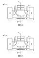
- FIG. 2schematically illustrates an embodiment of a memory cell 50 according to the present invention.
- the cell 50includes a substrate 12 of a first conductivity type, such as a p-type conductivity type, for example.
- Substrate 12is typically made of silicon, but may comprise germanium, silicon germanium, gallium arsenide, carbon nanotubes, or other semiconductor materials known in the art.
- the substrate 12has a surface 14 .
- a first region 16 having a second conductivity type, such as n-type, for example,is provided in substrate 12 and which is exposed at surface 14 .
- a second region 18 having the second conductivity typeis also provided in substrate 12 , which is exposed at surface 14 and which is spaced apart from the first region 16 .
- First and second regions 16 and 18are formed by an implantation process formed on the material making up substrate 12 , according to any of implantation processes known and typically used in the art.
- a buried layer 22 of the second conductivity typeis also provided in the substrate 12 , buried in the substrate 12 , as shown. Region 22 is also formed by an ion implantation process on the material of substrate 12 .
- a body region 24 of the substrate 12is bounded by surface 14 , first and second regions 16 , 18 and insulating layers 26 (e.g. shallow trench isolation (STI)), which may be made of silicon oxide, for example. Insulating layers 26 insulate cell 50 from neighboring cells 50 when multiple cells 50 are joined to make a memory device.
- a floating gate or trapping layer 60is positioned in between the regions 16 and 18 , and above the surface 14 . Trapping layer/floating gate 60 is insulated from surface 14 by an insulating layer 62 .
- Insulating layer 62may be made of silicon oxide and/or other dielectric materials, including high-K dielectric materials, such as, but not limited to, tantalum peroxide, titanium oxide, zirconium oxide, hafnium oxide, and/or aluminum oxide.
- Floating gate/trapping layer 60may be made of polysilicon material. If a trapping layer is chosen, the trapping layer may be made from silicon nitride or silicon nanocrystal, etc. Whether a floating gate 60 or a trapping layer 60 is used, the function is the same, in that they hold data in the absence of power. The primary difference between the floating gate 60 and the trapping layer 60 is that the floating gate 60 is a conductor, while the trapping layer 60 is an insulator layer. Thus, typically one or the other of trapping layer 60 and floating gate 60 are employed in device 50 , but not both.
- a control gate 66is positioned above floating gate/trapping layer 60 and insulated therefrom by insulating layer 64 such that floating gate/trapping layer 60 is positioned between insulating layer 62 and surface 14 underlying floating gate/trapping layer 60 , and insulating layer 64 and control gate 66 positioned above floating gate/trapping layer 60 , as shown.
- Control gate 66is capacitively coupled to floating gate/trapping layer 60 .
- Control gate 66is typically made of polysilicon material or metal gate electrode, such as tungsten, tantalum, titanium and their nitrides.
- the relationship between the floating gate/trapping layer 60 and control gate 66is similar to that of a nonvolatile stacked gate floating gate/trapping layer memory cell.
- the floating gate/trapping layer 60functions to store non-volatile memory data and the control gate 66 is used for memory cell selection.
- Cell 50includes four terminals: word line (WL) terminal 70 , source line (SL) terminal 72 , bit line (BL) terminal 74 and buried well (BW) terminal 76 .
- Terminal 70is connected to control gate 66 .
- Terminal 72is connected to first region 16 and terminal 74 is connected to second region 18 .
- terminal 72can be connected to second region 18 and terminal 74 can be connected to first region 16 .
- Terminal 76is connected to buried layer 22 .
- cell 50When power is applied to cell 50 , cell 50 operates like a currently available capacitorless DRAM cell.
- the memory informationi.e., data that is stored in memory
- the memory informationis stored as charge in the floating body of the transistor, i.e., in the body 24 of cell 50 .
- the presence of the electrical charge in the floating body 24modulates the threshold voltage of the cell 50 , which determines the state of the cell 50 .
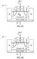
- FIGS. 3A-3Billustrate alternative write state “1” operations that can be carried out on cell 50 , by performing band-to-band tunneling hot hole injection ( FIG. 3A ) or impact ionization hot hole injection ( FIG. 3B ).
- electronscan be transferred, rather than holes.
- FIG. 3Ato write a state “1” into the floating body region 24 , a substantially neutral voltage is applied to SL terminal 72 , a positive voltage is applied to BL terminal 74 , a negative voltage is applied to WL terminal 70 and a positive voltage less than the positive voltage applied to the BL terminal 74 is applied to BW terminal 76 .
- a charge of about 0.0 voltsis applied to terminal 72
- a charge of about +2.0 voltsis applied to terminal 74
- a charge of about ⁇ 1.2 voltsis applied to terminal 70
- a charge of about +0.6 voltsis applied to terminal 76 .
- these voltage levelsmay vary, while maintaining the relative relationships between the charges applied, as described above.
- voltage applied to terminal 72may be in the range of about 0.0 volts to about +0.4 volts
- voltage applied to terminal 74may be in the range of about +1.5 volts to about +3.0 volts
- voltage applied to terminal 70may be in the range of about 0.0 volts to about ⁇ 3.0 volts
- voltage applied to terminal 76may be in the range of about 0.0 volts to about +1.0 volts.
- the voltages applied to terminals 72 and 74may be reversed, and still obtain the same result, e.g., a positive voltage applied to terminal 72 and a neutral charge applied to terminal 74 .
- a substantially neutral voltageis applied to SL terminal 72
- a positive voltageis applied to BL terminal 74
- a positive voltage less positive than the positive voltage applied to terminal 72is applied to WL terminal 70
- a positive voltage less positive than the positive voltage applied to terminal 74is applied to BW terminal 76 .
- holesare injected from BL terminal 74 into the floating body region 24 , leaving the body region 24 positively charged.
- about 0.0 voltsis applied to terminal 72
- about +2.0 voltsis applied to terminal 74
- about +1.2 voltsis applied to terminal 70
- about +0.6 voltsis applied to terminal 76 .
- these voltage levelsmay vary, while maintaining the relative relationships between the charges applied, as described above.
- voltage applied to terminal 72may be in the range of about 0.0 volts to about +0.6 volts
- voltage applied to terminal 74may be in the range of about +1.5 volts to about +3.0 volts
- voltage applied to terminal 70may be in the range of about 0.0 volts to about +1.6 volts
- voltage applied to terminal 76may be in the range of about 0.0 volts to about 1.0 volts.
- the voltages applied to terminals 72 and 74may be reversed, and still obtain the same result, e.g., a positive voltage applied to terminal 72 and a neutral charge applied to terminal 74 .
- FIG. 4illustrates a write state “0” operation that can be carried out on cell 50 .
- a negative voltageis applied to SL terminal 72
- a substantially neutral voltageis applied to BL terminal 74
- a negative voltage less negative than the negative voltage applied to terminal 72is applied to WL terminal 70 and a positive voltage is applied to BW terminal 76 .
- the p-n junctionjunction between 24 and 16 and between 24 and 18 ) is forward-biased, evacuating any holes from the floating body 24 .
- ⁇ 2.0 voltsis applied to terminal 72
- about 0.0 voltsis applied to terminal 74
- about ⁇ 1.2 voltsis applied to terminal 70
- about +0.6 voltsis applied to terminal 76 .
- these voltage levelsmay vary, while maintaining the relative relationships between the charges applied, as described above.
- voltage applied to terminal 72may be in the range of about ⁇ 1.0 volts to about ⁇ 3.0 volts
- voltage applied to terminal 74may be in the range of about 0.0 volts to about ⁇ 3.0 volts
- voltage applied to terminal 70may be in the range of about 0.0 volts to about ⁇ 3.0 volts
- voltage applied to terminal 76may be in the range of about 0.0 volts to about 1.0 volts.
- the voltages applied to terminals 72 and 74may be reversed, and still obtain the same result, e.g., a substantially neutral voltage applied to terminal 72 and a negative charge applied to terminal 74 .
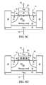
- a read operation of the cell 50is now described with reference to FIG. 5 .
- a substantially neutral charge voltsis applied to SL terminal 72
- a positive voltageis applied to BL terminal 74
- a positive voltage that is more positive than the positive voltage applied to terminal 74is applied to WL terminal 70
- a positive voltage that is less than the positive voltage applied to terminal 70is applied to BW terminal 76 . If cell 50 is in a state “1” having holes in the body region 24 , then a lower threshold voltage (gate voltage where the transistor is turned on) is observed compared to the threshold voltage observed when cell 50 is in a state “0” having no holes in body region 24 .
- about 0.0 voltsis applied to terminal 72
- about +0.4 voltsis applied to terminal 74
- about +1.2 voltsis applied to terminal 70
- about +0.6 voltsis applied to terminal 76 .
- these voltage levelsmay vary, while maintaining the relative relationships between the charges applied, as described above.
- terminal 72is grounded and is thus at about 0.0 volts
- voltage applied to terminal 74may be in the range of about +0.1 volts to about +1.0 volts
- voltage applied to terminal 70may be in the range of about +1.0 volts to about +3.0 volts
- voltage applied to terminal 76may be in the range of about 0.0 volts to about 1.0 volts.
- the voltages applied to terminals 72 and 74may be reversed, and still obtain the same result, e.g., a positive voltage applied to terminal 72 and a neutral charge applied to terminal 74 .
- ShadowingWhen power down is detected, e.g., when a user turns off the power to cell 50 , or the power is inadvertently interrupted, or for any other reason, power is at least temporarily discontinued to cell 50 , data stored in the floating body region 24 is transferred to floating gate/trapping layer 60 .
- This operationis referred to as “shadowing” and is described with reference to FIGS. 6A and 6B .
- both SL terminal 72 and BL terminal 74are left floating (i.e., not held to any specific voltage, but allowed to float to their respective voltages).
- a high positive voltage(e.g., about +18 volts) is applied to WL terminal 70 and a low positive voltage (e.g., about +0.6 volts) is applied to BW terminal 76 .
- a low positive voltagee.g., about +0.6 volts
- terminals 72 and 74are allowed to float, about +18 volts is applied to terminal 70 , and about +0.6 volts is applied to terminal 76 .
- these voltage levelsmay vary, while maintaining the relative relationships between the charges applied, as described above.
- voltage applied to terminal 70may be in the range of about +12.0 volts to about +20.0 volts
- voltage applied to terminal 76may be in the range of about 0.0 volts to about 1.0 volts.
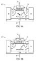
- the state of the cell 50 as stored on floating gate/trapping layer 60is restored into floating body region 24 .
- the restore operationdata restoration from non-volatile memory to volatile memory
- the floating body 24is set to a positive charge, i.e., a “1” state is written to floating body 24 .
- both SL terminal 72 and BL terminal 74are left floating. A large negative voltage is applied to WL terminal 70 and a low positive voltage is applied to BW terminal 76 .
- the floating gate/trapping layer 60is not negatively charged, no electrons will tunnel from floating gate/trapping layer 60 to floating body 24 , and cell 50 will therefore be in a state “1”. Conversely, if floating gate/trapping layer 60 is negatively charged, electrons tunnel from floating gate/trapping layer 60 into floating body 24 , thereby placing cell 50 in a state “0”.
- about ⁇ 18.0 voltsis applied to terminal 70
- about +0.6 voltsis applied to terminal 76 .
- these voltage levelsmay vary, while maintaining the relative relationships between the charges applied, as described above.
- voltage applied to terminal 70may be in the range of about ⁇ 12.0 volts to about ⁇ 20.0 volts
- voltage applied to terminal 76may be in the range of about 0.0 volts to about +1.0 volts.
- this processoccurs non-algorithmically, as the state of the floating gate/trapping layer 60 does not have to be read, interpreted, or otherwise measure to determine what state to restore the floating body 24 to. Rather, the restoration process occurs automatically, driven by electrical potential differences. Accordingly, this process is orders of magnitude faster than one that requires algorithmic intervention. Similarly, it is noted that the shadowing process also is performed as a non-algorithmic process. From these operations, it has been shown that cell 50 provides a memory cell having the advantages of a DRAM cell, but where non-volatility is also achieved.
- FIGS. 8A-8Dillustrate another embodiment of operation of cell 50 to perform a volatile to non-volatile shadowing process, which operates by a hot electron injection process, in contrast to the tunneling process (e.g., Fowler-Nordheim tunneling process) described above with regard to FIGS. 6A-6B .
- FIG. 8Eillustrates the operation of an NPN bipolar device 90 , as it relates to the operation of cell 50 .
- Floating body 24is represented by the terminal to which voltage V FB is applied in FIG. 8E
- the terminals 72 and 74are represented by terminals to which voltages V SL and V BL are applied, respectively.
- V FBWhen V FB is a positive voltage, this turns on the bipolar device 90 , and when V FB is a negative or neutral voltage, the device 90 is turned off.
- V FBWhen V FB is a positive voltage, this turns on the bipolar device 90 , and when V FB is a negative or neutral voltage, the device 90 is turned off.
- floating body 24has a positive voltage, this turns on the cell 50 so that current flows through the NPN junction formed by 16 , 24 and 18 in the direction indicated by the arrow in floating body 24 in FIG. 8A , and when floating body 24 has a negative or neutral voltage, cell is turned off, so that there is no current flow through the NPN junction.
- a high positive voltageis applied to terminal 72 and a substantially neutral voltage is applied to terminal 74 .
- a high positive voltagecan be applied to terminal 74 and a substantially neutral voltage can be applied to terminal 72 .
- a positive voltageis applied to terminal 70 and a low positive voltage is applied to terminal 76 .
- a high voltage in this caseis a voltage greater than or equal to about +3 volts. In one example, a voltage in the range of about +3 to about +6 volts is applied, although it is possible to apply a higher voltage.
- the floating gate/trapping layer 60will have been previously initialized or reset to have a positive charge prior to the operation of the cell 50 to store data in non-volatile memory via floating body 24 .
- the NPN junctionis on, as noted above, and electrons flow in the direction of the arrow shown in the floating body 24 in FIG. 8A .
- the application of the high voltage to terminal 72 at 16energizes/accelerates electrons traveling through the floating body 24 to a sufficient extent that they can “jump over” the oxide barrier between floating body 24 and floating gate/trapping layer 60 , so that electrons enter floating gate/trapping layer 60 as indicated by the arrow into floating gate/trapping layer 60 in FIG. 8A .
- floating gate/trapping layer 60becomes negatively charged by the shadowing process, when the volatile memory of cell 50 is in state “1” (i.e., floating body 24 is positively charged), as shown in FIG. 8B .
- the charge state of the floating gate/trapping layer 60is complementary to the charge state of the floating body 24 after completion of the shadowing process.
- the floating gate/trapping layer 60will become negatively charged by the shadowing process, whereas if the floating body of the memory cell 50 has a negative or neutral charge in volatile memory, the floating gate/trapping layer 60 will be positively charged at the end of the shadowing operation.
- the charges/states of the floating gates/trapping layers 60are determined non-algorithmically by the states of the floating bodies, and shadowing of multiple cells occurs in parallel, therefore the shadowing process is very fast.
- voltage applied to terminal 72may be in the range of about +3 volts to about +6 volts
- the voltage applied to terminal 74may be in the range of about 0.0 volts to about +0.4 volts
- the voltage applied to terminal 70may be in the range of about 0.0 volts to about +1.6 volts
- voltage applied to terminal 76may be in the range of about 0.0 volts to about +1.0 volts.
- FIGS. 9A-9Banother embodiment of operation of cell 50 to perform a restore process from non-volatile to volatile memory is schematically illustrated, in which the restore process operates by a band-to-band tunneling hot hole injection process (modulated by the floating gate/trapping layer 60 charge), in contrast to the electron tunneling process described above with regard to FIGS. 7A-7B .
- the floating body 24is set to a neutral or negative charge prior to the performing the restore operation/process, i.e., a “0” state is written to floating body 24 .
- FIGS. 9A-9Bthe floating body 24 is set to a neutral or negative charge prior to the performing the restore operation/process, i.e., a “0” state is written to floating body 24 .
- terminal 72is set to a substantially neutral voltage, a positive voltage is applied to terminal 74 , a negative voltage is applied to terminal 70 and a positive voltage that is less positive than the positive voltage applied to terminal 74 is applied to terminal 76 .
- this negative chargeenhances the driving force for the band-to-band hot hole injection process, whereby holes are injected from the n-region 18 into floating body 24 , thereby restoring the “1” state that the volatile memory cell 50 had held prior to the performance of the shadowing operation.
- the floating gate/trapping layer 60is not negatively charged, such as when the floating gate/trapping layer 60 is positively charged as shown in FIG.
- 0 voltsis applied to terminal 72
- about +2 voltsis applied to terminal 74
- about ⁇ 1.2 voltsis applied to terminal 70
- about +0.6 voltsis applied to terminal 76 .
- these voltage levelsmay vary, while maintaining the relative relationships between the charges applied, as described above.
- voltage applied to terminal 72may be in the range of about +1.5 volts to about +3.0 volts
- voltage applied to terminal 74may be in the range of about 0.0 volts to about +0.6 volts
- voltage applied to terminal 70may be in the range of about 0.0 volts to about ⁇ 3.0 volts
- voltage applied to terminal 76may be in the range of about 0.0 volts to about +1.0 volts.
- the floating gate(s)/trapping layer(s) 60is/are reset to a predetermined state, e.g., a positive state as illustrated in FIG. 10 , so that each floating gate/trapping layer 60 has a known state prior to performing another shadowing operation.
- the reset processoperates by the mechanism of electron tunneling from the floating gate/trapping layer 60 to the source region 18 , as illustrated in FIG. 10 .
- a highly negative voltageis applied to terminal 70
- a substantially neutral voltageis applied to SL terminal 72
- BL terminal 74is allowed to float or is grounded
- a positive voltageis applied to terminal 76 .
- region 16By applying a neutral voltage to terminal 72 and maintaining the voltage of region 16 to be substantially neutral, this causes region 16 to function as a sink for the electrons from floating gate/trapping layer 60 to travel to by electron tunneling.
- a large negative voltagesis applied to WL terminal 70 and a low positive voltage is applied to BW terminal 76 . If the floating gate/trapping layer 60 is negatively charged, electrons will tunnel from floating gate/trapping layer 60 to region 16 , and floating gate/trapping layer 60 will therefore become positively charged.
- ⁇ 18.0 voltsis applied to terminal 70
- +0.6 voltsis applied to terminal 76 .
- these voltage levelsmay vary, while maintaining the relative relationships between the charges applied, as described above.
- voltage applied to terminal 70may be in the range of about ⁇ 12.0 volts to about ⁇ 20.0 volts
- the voltage applied to terminal 76may be in the range of about 0.0 volts to about 1.0 volts.
- FIG. 1describes operation of a memory device having a plurality of memory cells 50 .
- the number of memory cellscan vary widely, for example ranging from less than 100 Mb to several Gb, or more. It is noted that, except for the DRAM operations of writing and reading (event 104 ), which by necessity must be capable of individual, controlled operations, the remaining operations shown in FIG. 1 can all be carried out as parallel, non-algorithmic operations, which results in a very fast operating memory device.
- the memory deviceis initialized by first setting all of the floating gates/trapping layers to a positive state, in a manner as described above with reference to FIG. 10 , for example.
- a control linecan be used to input a highly negative voltage to each of terminals 70 , in parallel, with voltage settings at the other terminals as described above with reference to FIG. 10 .
- Individual bits (or multiple bits, as described below) of datacan be read from or written to floating bodies 24 of the respective cells at event 104 .
- the shadowing operation at event 106is conducted in a mass parallel, non-algorithmic process, in any of the same manners described above, with each of the cells 50 performing the shadowing operation simultaneously, in a parallel operation. Because no algorithmic interpretation or measurement is required to transfer the data from non-volatile to volatile memory ( 24 to 60 ), the shadowing operation is very fast and efficient.
- a state “0”is first written into each of the floating bodies 24 , by a parallel process, and then each of the floating bodies is restored in any of the same manners described above with regard to a restoration process of a single floating body 24 .
- This processis also a mass, parallel non-algorithmic process, so that no algorithmic processing or measurement of the states of the floating gates/trapping layers 60 is required prior to transferring the data stored by the floating gates/trapping layers 60 to the floating bodies 24 .
- the floating bodiesare restored simultaneously, in parallel, in a very fast and efficient process.
- the floating gates/trapping layers 60are then reset at event 110 , to establish a positive charge in each of the floating gates/trapping layers, in the same manner as described above with regard to initializing at event 110 .
- FIG. 11Aillustrates the states of a binary cell, relative to threshold voltage, wherein a voltage less than or equal to a predetermined voltage (in one example, the predetermined voltage is 0 volts, but the predetermined voltage may be a higher or lower voltage) in floating body 24 is interpreted as state “0”, and a voltage greater than the predetermined voltage in floating body 24 is interpreted as state “1”.
- a predetermined voltagein one example, the predetermined voltage is 0 volts, but the predetermined voltage may be a higher or lower voltage
- the memory cells described hereincan be configured to function as multi-level cells, so that more than one bit of data can be stored in each cell 50 .
- 11Billustrates an example of voltage states of a multi-level cell wherein two bits of data can be stored in each cell 50 .
- a voltage less than or equal to a first predetermined voltagee.g., 0 volts or some other predetermined voltage
- a second predetermined voltagethat is less than the first predetermined voltage (e.g., about ⁇ 0.5 volts or some other voltage less than the first predetermined voltage) in floating body 24 volts
- a voltage less than or equal to the second predetermined voltageis interpreted as state “00”
- a voltage greater than the first predetermined voltage and less than or equal to a third predetermined voltage that is greater than the first predetermined voltagee.g., about +0.5 volts or some other predetermined voltage that is greater than the first predetermined voltage
- a third predetermined voltageis interpreted to be state “10” and a voltage greater than the third predetermined voltage is interpreted as state “11”.
Landscapes
- Engineering & Computer Science (AREA)
- Microelectronics & Electronic Packaging (AREA)
- Computer Hardware Design (AREA)
- Non-Volatile Memory (AREA)
Abstract
Description
Claims (20)
Priority Applications (1)
| Application Number | Priority Date | Filing Date | Title |
|---|---|---|---|
| US13/758,646US8570803B2 (en) | 2006-11-29 | 2013-02-04 | Semiconductor memory having both volatile and non-volatile functionality and method of operating |
Applications Claiming Priority (5)
| Application Number | Priority Date | Filing Date | Title |
|---|---|---|---|
| US86177806P | 2006-11-29 | 2006-11-29 | |
| US11/998,311US7760548B2 (en) | 2006-11-29 | 2007-11-29 | Semiconductor memory having both volatile and non-volatile functionality and method of operating |
| US12/797,164US8036033B2 (en) | 2006-11-29 | 2010-06-09 | Semiconductor memory having both volatile and non-volatile functionality and method of operating |
| US13/231,188US8391066B2 (en) | 2006-11-29 | 2011-09-13 | Semiconductor memory having both volatile and non-volatile functionality and method of operating |
| US13/758,646US8570803B2 (en) | 2006-11-29 | 2013-02-04 | Semiconductor memory having both volatile and non-volatile functionality and method of operating |
Related Parent Applications (1)
| Application Number | Title | Priority Date | Filing Date |
|---|---|---|---|
| US13/231,188ContinuationUS8391066B2 (en) | 2006-11-29 | 2011-09-13 | Semiconductor memory having both volatile and non-volatile functionality and method of operating |
Publications (2)
| Publication Number | Publication Date |
|---|---|
| US20130148422A1 US20130148422A1 (en) | 2013-06-13 |
| US8570803B2true US8570803B2 (en) | 2013-10-29 |
Family
ID=39463512
Family Applications (4)
| Application Number | Title | Priority Date | Filing Date |
|---|---|---|---|
| US11/998,311Active2029-01-06US7760548B2 (en) | 2006-11-29 | 2007-11-29 | Semiconductor memory having both volatile and non-volatile functionality and method of operating |
| US12/797,164ActiveUS8036033B2 (en) | 2006-11-29 | 2010-06-09 | Semiconductor memory having both volatile and non-volatile functionality and method of operating |
| US13/231,188Expired - Fee RelatedUS8391066B2 (en) | 2006-11-29 | 2011-09-13 | Semiconductor memory having both volatile and non-volatile functionality and method of operating |
| US13/758,646ActiveUS8570803B2 (en) | 2006-11-29 | 2013-02-04 | Semiconductor memory having both volatile and non-volatile functionality and method of operating |
Family Applications Before (3)
| Application Number | Title | Priority Date | Filing Date |
|---|---|---|---|
| US11/998,311Active2029-01-06US7760548B2 (en) | 2006-11-29 | 2007-11-29 | Semiconductor memory having both volatile and non-volatile functionality and method of operating |
| US12/797,164ActiveUS8036033B2 (en) | 2006-11-29 | 2010-06-09 | Semiconductor memory having both volatile and non-volatile functionality and method of operating |
| US13/231,188Expired - Fee RelatedUS8391066B2 (en) | 2006-11-29 | 2011-09-13 | Semiconductor memory having both volatile and non-volatile functionality and method of operating |
Country Status (1)
| Country | Link |
|---|---|
| US (4) | US7760548B2 (en) |
Cited By (35)
| Publication number | Priority date | Publication date | Assignee | Title |
|---|---|---|---|---|
| US9029922B2 (en) | 2013-03-09 | 2015-05-12 | Zeno Semiconductor, Inc. | Memory device comprising electrically floating body transistor |
| US9030872B2 (en) | 2007-11-29 | 2015-05-12 | Zeno Semiconductor, Inc. | Method of maintaining the state of semiconductor memory having electrically floating body transistor |
| US9209188B2 (en) | 2007-11-29 | 2015-12-08 | Zeno Semiconductor, Inc. | Compact semiconductor memory device having reduced number of contacts, methods of operating and methods of making |
| US9230965B2 (en) | 2008-08-05 | 2016-01-05 | Zeno Semiconductor, Inc. | Method of operating semiconductor memory device with floating body transistor using silicon controlled rectifier principle |
| US9257179B2 (en) | 2008-04-08 | 2016-02-09 | Zeno Semiconductor, Inc. | Semiconductor memory having volatile and multi-bit non-volatile functionality and method of operating |
| US9275723B2 (en) | 2013-04-10 | 2016-03-01 | Zeno Semiconductor, Inc. | Scalable floating body memory cell for memory compilers and method of using floating body memories with memory compilers |
| US9368625B2 (en) | 2013-05-01 | 2016-06-14 | Zeno Semiconductor, Inc. | NAND string utilizing floating body memory cell |
| US9391079B2 (en) | 2007-11-29 | 2016-07-12 | Zeno Semiconductor, Inc. | Compact semiconductor memory device having reduced number of contacts, methods of operating and methods of making |
| US9401206B2 (en) | 2011-10-13 | 2016-07-26 | Zeno Semiconductor, Inc. | Semiconductor memory having both volatile and non-volatile functionality comprising resistive change material and method of operating |
| US9455262B2 (en) | 2010-02-07 | 2016-09-27 | Zeno Semiconductor, Inc. | Semiconductor device having electrically floating body transistor, semiconductor device having both volatile and non-volatile functionality and method of operating |
| US9460790B2 (en) | 2007-10-24 | 2016-10-04 | Zeno Semiconductor, Inc. | Semiconductor memory having both volatile and non-volatile functionality and method of operating |
| US9490012B2 (en) | 2008-08-22 | 2016-11-08 | Zeno Semiconductor, Inc. | Semiconductor memory having both volatile and non-volatile functionality including resistance change material and method of operating |
| US9496053B2 (en) | 2014-08-15 | 2016-11-15 | Zeno Semiconductor, Inc. | Memory device comprising electrically floating body transistor |
| US9524970B2 (en) | 2011-03-24 | 2016-12-20 | Zeno Semiconductor, Inc. | Asymmetric semiconductor memory device having electrically floating body transistor |
| US9536595B2 (en) | 2013-07-10 | 2017-01-03 | Zeno Semiconductor, Inc. | Systems and methods for reducing standby power in floating body memory devices |
| US9548119B2 (en) | 2014-01-15 | 2017-01-17 | Zeno Semiconductor, Inc | Memory device comprising an electrically floating body transistor |
| US9576962B2 (en) | 2012-04-08 | 2017-02-21 | Zeno Semiconductor, Inc. | Memory device having electrically floating body transistor |
| US9589963B2 (en) | 2010-11-16 | 2017-03-07 | Zeno Semiconductor, Inc. | Dual-port semiconductor memory and first in first out (FIFO) memory having electrically floating body transistor |
| US9601493B2 (en) | 2006-11-29 | 2017-03-21 | Zeno Semiconductor, Inc | Compact semiconductor memory device having reduced number of contacts, methods of operating and methods of making |
| US9679648B2 (en) | 2007-11-29 | 2017-06-13 | Zeno Semiconductor, Inc. | Memory cells, memory cell arrays, methods of using and methods of making |
| US9704870B2 (en) | 2010-03-02 | 2017-07-11 | Zeno Semiconductors, Inc. | Compact semiconductor memory device having reduced number of contacts, methods of operating and methods of making |
| US9922981B2 (en) | 2010-03-02 | 2018-03-20 | Zeno Semiconductor, Inc. | Compact semiconductor memory device having reduced number of contacts, methods of operating and methods of making |
| US10079301B2 (en) | 2016-11-01 | 2018-09-18 | Zeno Semiconductor, Inc. | Memory device comprising an electrically floating body transistor and methods of using |
| USRE47381E1 (en) | 2008-09-03 | 2019-05-07 | Zeno Semiconductor, Inc. | Forming semiconductor cells with regions of varying conductivity |
| US10340276B2 (en) | 2010-03-02 | 2019-07-02 | Zeno Semiconductor, Inc. | Method of maintaining the state of semiconductor memory having electrically floating body transistor |
| US10373685B2 (en) | 2013-01-14 | 2019-08-06 | Zeno Semiconductor, Inc. | Content addressable memory device having electrically floating body transistor |
| US10403361B2 (en) | 2007-11-29 | 2019-09-03 | Zeno Semiconductor, Inc. | Memory cells, memory cell arrays, methods of using and methods of making |
| US10461084B2 (en) | 2010-03-02 | 2019-10-29 | Zeno Semiconductor, Inc. | Compact semiconductor memory device having reduced number of contacts, methods of operating and methods of making |
| US10553683B2 (en) | 2015-04-29 | 2020-02-04 | Zeno Semiconductor, Inc. | MOSFET and memory cell having improved drain current through back bias application |
| US11201215B2 (en) | 2015-04-29 | 2021-12-14 | Zeno Semiconductor, Inc. | MOSFET and memory cell having improved drain current through back bias application |
| US11404419B2 (en) | 2018-04-18 | 2022-08-02 | Zeno Semiconductor, Inc. | Memory device comprising an electrically floating body transistor |
| US11600663B2 (en) | 2019-01-11 | 2023-03-07 | Zeno Semiconductor, Inc. | Memory cell and memory array select transistor |
| US11908899B2 (en) | 2009-02-20 | 2024-02-20 | Zeno Semiconductor, Inc. | MOSFET and memory cell having improved drain current through back bias application |
| US11974425B2 (en) | 2012-02-16 | 2024-04-30 | Zeno Semiconductor, Inc. | Memory cell comprising first and second transistors and methods of operating |
| US12439611B2 (en) | 2019-03-12 | 2025-10-07 | Zeno Semiconductor, Inc. | Memory cell and memory array select transistor |
Families Citing this family (157)
| Publication number | Priority date | Publication date | Assignee | Title |
|---|---|---|---|---|
| US7760548B2 (en)* | 2006-11-29 | 2010-07-20 | Yuniarto Widjaja | Semiconductor memory having both volatile and non-volatile functionality and method of operating |
| US7554851B2 (en)* | 2007-01-05 | 2009-06-30 | Macronix International Co., Ltd. | Reset method of non-volatile memory |
| US8264875B2 (en) | 2010-10-04 | 2012-09-11 | Zeno Semiconducor, Inc. | Semiconductor memory device having an electrically floating body transistor |
| US8174886B2 (en) | 2007-11-29 | 2012-05-08 | Zeno Semiconductor, Inc. | Semiconductor memory having electrically floating body transistor |
| US8130548B2 (en)* | 2007-11-29 | 2012-03-06 | Zeno Semiconductor, Inc. | Semiconductor memory having electrically floating body transistor |
| US8148780B2 (en) | 2009-03-24 | 2012-04-03 | Micron Technology, Inc. | Devices and systems relating to a memory cell having a floating body |
| US11374118B2 (en) | 2009-10-12 | 2022-06-28 | Monolithic 3D Inc. | Method to form a 3D integrated circuit |
| US12027518B1 (en) | 2009-10-12 | 2024-07-02 | Monolithic 3D Inc. | 3D semiconductor devices and structures with metal layers |
| US10910364B2 (en) | 2009-10-12 | 2021-02-02 | Monolitaic 3D Inc. | 3D semiconductor device |
| US11018133B2 (en) | 2009-10-12 | 2021-05-25 | Monolithic 3D Inc. | 3D integrated circuit |
| US11984445B2 (en) | 2009-10-12 | 2024-05-14 | Monolithic 3D Inc. | 3D semiconductor devices and structures with metal layers |
| US12362219B2 (en) | 2010-11-18 | 2025-07-15 | Monolithic 3D Inc. | 3D semiconductor memory device and structure |
| US11482440B2 (en) | 2010-12-16 | 2022-10-25 | Monolithic 3D Inc. | 3D semiconductor device and structure with a built-in test circuit for repairing faulty circuits |
| US11469271B2 (en) | 2010-10-11 | 2022-10-11 | Monolithic 3D Inc. | Method to produce 3D semiconductor devices and structures with memory |
| US11227897B2 (en) | 2010-10-11 | 2022-01-18 | Monolithic 3D Inc. | Method for producing a 3D semiconductor memory device and structure |
| US10896931B1 (en) | 2010-10-11 | 2021-01-19 | Monolithic 3D Inc. | 3D semiconductor device and structure |
| US11158674B2 (en) | 2010-10-11 | 2021-10-26 | Monolithic 3D Inc. | Method to produce a 3D semiconductor device and structure |
| US11018191B1 (en) | 2010-10-11 | 2021-05-25 | Monolithic 3D Inc. | 3D semiconductor device and structure |
| US11600667B1 (en) | 2010-10-11 | 2023-03-07 | Monolithic 3D Inc. | Method to produce 3D semiconductor devices and structures with memory |
| US11024673B1 (en) | 2010-10-11 | 2021-06-01 | Monolithic 3D Inc. | 3D semiconductor device and structure |
| US11315980B1 (en) | 2010-10-11 | 2022-04-26 | Monolithic 3D Inc. | 3D semiconductor device and structure with transistors |
| US11257867B1 (en) | 2010-10-11 | 2022-02-22 | Monolithic 3D Inc. | 3D semiconductor device and structure with oxide bonds |
| US10833108B2 (en) | 2010-10-13 | 2020-11-10 | Monolithic 3D Inc. | 3D microdisplay device and structure |
| US11043523B1 (en) | 2010-10-13 | 2021-06-22 | Monolithic 3D Inc. | Multilevel semiconductor device and structure with image sensors |
| US11437368B2 (en) | 2010-10-13 | 2022-09-06 | Monolithic 3D Inc. | Multilevel semiconductor device and structure with oxide bonding |
| US11855114B2 (en) | 2010-10-13 | 2023-12-26 | Monolithic 3D Inc. | Multilevel semiconductor device and structure with image sensors and wafer bonding |
| US12080743B2 (en) | 2010-10-13 | 2024-09-03 | Monolithic 3D Inc. | Multilevel semiconductor device and structure with image sensors and wafer bonding |
| US11694922B2 (en) | 2010-10-13 | 2023-07-04 | Monolithic 3D Inc. | Multilevel semiconductor device and structure with oxide bonding |
| US11063071B1 (en) | 2010-10-13 | 2021-07-13 | Monolithic 3D Inc. | Multilevel semiconductor device and structure with waveguides |
| US11869915B2 (en) | 2010-10-13 | 2024-01-09 | Monolithic 3D Inc. | Multilevel semiconductor device and structure with image sensors and wafer bonding |
| US10943934B2 (en) | 2010-10-13 | 2021-03-09 | Monolithic 3D Inc. | Multilevel semiconductor device and structure |
| US10978501B1 (en) | 2010-10-13 | 2021-04-13 | Monolithic 3D Inc. | Multilevel semiconductor device and structure with waveguides |
| US10998374B1 (en) | 2010-10-13 | 2021-05-04 | Monolithic 3D Inc. | Multilevel semiconductor device and structure |
| US11404466B2 (en) | 2010-10-13 | 2022-08-02 | Monolithic 3D Inc. | Multilevel semiconductor device and structure with image sensors |
| US11855100B2 (en) | 2010-10-13 | 2023-12-26 | Monolithic 3D Inc. | Multilevel semiconductor device and structure with oxide bonding |
| US12094892B2 (en) | 2010-10-13 | 2024-09-17 | Monolithic 3D Inc. | 3D micro display device and structure |
| US11164898B2 (en) | 2010-10-13 | 2021-11-02 | Monolithic 3D Inc. | Multilevel semiconductor device and structure |
| US11133344B2 (en) | 2010-10-13 | 2021-09-28 | Monolithic 3D Inc. | Multilevel semiconductor device and structure with image sensors |
| US11984438B2 (en) | 2010-10-13 | 2024-05-14 | Monolithic 3D Inc. | Multilevel semiconductor device and structure with oxide bonding |
| US11163112B2 (en) | 2010-10-13 | 2021-11-02 | Monolithic 3D Inc. | Multilevel semiconductor device and structure with electromagnetic modulators |
| US11605663B2 (en) | 2010-10-13 | 2023-03-14 | Monolithic 3D Inc. | Multilevel semiconductor device and structure with image sensors and wafer bonding |
| US11929372B2 (en) | 2010-10-13 | 2024-03-12 | Monolithic 3D Inc. | Multilevel semiconductor device and structure with image sensors and wafer bonding |
| US11327227B2 (en) | 2010-10-13 | 2022-05-10 | Monolithic 3D Inc. | Multilevel semiconductor device and structure with electromagnetic modulators |
| US12360310B2 (en) | 2010-10-13 | 2025-07-15 | Monolithic 3D Inc. | Multilevel semiconductor device and structure with oxide bonding |
| US11569117B2 (en) | 2010-11-18 | 2023-01-31 | Monolithic 3D Inc. | 3D semiconductor device and structure with single-crystal layers |
| US12033884B2 (en) | 2010-11-18 | 2024-07-09 | Monolithic 3D Inc. | Methods for producing a 3D semiconductor device and structure with memory cells and multiple metal layers |
| US11004719B1 (en) | 2010-11-18 | 2021-05-11 | Monolithic 3D Inc. | Methods for producing a 3D semiconductor memory device and structure |
| US11107721B2 (en) | 2010-11-18 | 2021-08-31 | Monolithic 3D Inc. | 3D semiconductor device and structure with NAND logic |
| US11482439B2 (en) | 2010-11-18 | 2022-10-25 | Monolithic 3D Inc. | Methods for producing a 3D semiconductor memory device comprising charge trap junction-less transistors |
| US11355381B2 (en) | 2010-11-18 | 2022-06-07 | Monolithic 3D Inc. | 3D semiconductor memory device and structure |
| US11211279B2 (en) | 2010-11-18 | 2021-12-28 | Monolithic 3D Inc. | Method for processing a 3D integrated circuit and structure |
| US11508605B2 (en) | 2010-11-18 | 2022-11-22 | Monolithic 3D Inc. | 3D semiconductor memory device and structure |
| US12125737B1 (en) | 2010-11-18 | 2024-10-22 | Monolithic 3D Inc. | 3D semiconductor device and structure with metal layers and memory cells |
| US11094576B1 (en) | 2010-11-18 | 2021-08-17 | Monolithic 3D Inc. | Methods for producing a 3D semiconductor memory device and structure |
| US11355380B2 (en) | 2010-11-18 | 2022-06-07 | Monolithic 3D Inc. | Methods for producing 3D semiconductor memory device and structure utilizing alignment marks |
| US11521888B2 (en) | 2010-11-18 | 2022-12-06 | Monolithic 3D Inc. | 3D semiconductor device and structure with high-k metal gate transistors |
| US11031275B2 (en) | 2010-11-18 | 2021-06-08 | Monolithic 3D Inc. | 3D semiconductor device and structure with memory |
| US12272586B2 (en) | 2010-11-18 | 2025-04-08 | Monolithic 3D Inc. | 3D semiconductor memory device and structure with memory and metal layers |
| US12144190B2 (en) | 2010-11-18 | 2024-11-12 | Monolithic 3D Inc. | 3D semiconductor device and structure with bonding and memory cells preliminary class |
| US11854857B1 (en) | 2010-11-18 | 2023-12-26 | Monolithic 3D Inc. | Methods for producing a 3D semiconductor device and structure with memory cells and multiple metal layers |
| US11482438B2 (en) | 2010-11-18 | 2022-10-25 | Monolithic 3D Inc. | Methods for producing a 3D semiconductor memory device and structure |
| US12136562B2 (en) | 2010-11-18 | 2024-11-05 | Monolithic 3D Inc. | 3D semiconductor device and structure with single-crystal layers |
| US11901210B2 (en) | 2010-11-18 | 2024-02-13 | Monolithic 3D Inc. | 3D semiconductor device and structure with memory |
| US11164770B1 (en) | 2010-11-18 | 2021-11-02 | Monolithic 3D Inc. | Method for producing a 3D semiconductor memory device and structure |
| US11784082B2 (en) | 2010-11-18 | 2023-10-10 | Monolithic 3D Inc. | 3D semiconductor device and structure with bonding |
| US11735462B2 (en) | 2010-11-18 | 2023-08-22 | Monolithic 3D Inc. | 3D semiconductor device and structure with single-crystal layers |
| US12154817B1 (en) | 2010-11-18 | 2024-11-26 | Monolithic 3D Inc. | Methods for producing a 3D semiconductor memory device and structure |
| US11018042B1 (en) | 2010-11-18 | 2021-05-25 | Monolithic 3D Inc. | 3D semiconductor memory device and structure |
| US11610802B2 (en) | 2010-11-18 | 2023-03-21 | Monolithic 3D Inc. | Method for producing a 3D semiconductor device and structure with single crystal transistors and metal gate electrodes |
| US12100611B2 (en) | 2010-11-18 | 2024-09-24 | Monolithic 3D Inc. | Methods for producing a 3D semiconductor device and structure with memory cells and multiple metal layers |
| US12243765B2 (en) | 2010-11-18 | 2025-03-04 | Monolithic 3D Inc. | 3D semiconductor device and structure with metal layers and memory cells |
| US11804396B2 (en) | 2010-11-18 | 2023-10-31 | Monolithic 3D Inc. | Methods for producing a 3D semiconductor device and structure with memory cells and multiple metal layers |
| US11862503B2 (en) | 2010-11-18 | 2024-01-02 | Monolithic 3D Inc. | Method for producing a 3D semiconductor device and structure with memory cells and multiple metal layers |
| US12068187B2 (en) | 2010-11-18 | 2024-08-20 | Monolithic 3D Inc. | 3D semiconductor device and structure with bonding and DRAM memory cells |
| US11443971B2 (en) | 2010-11-18 | 2022-09-13 | Monolithic 3D Inc. | 3D semiconductor device and structure with memory |
| US11495484B2 (en) | 2010-11-18 | 2022-11-08 | Monolithic 3D Inc. | 3D semiconductor devices and structures with at least two single-crystal layers |
| US11923230B1 (en) | 2010-11-18 | 2024-03-05 | Monolithic 3D Inc. | 3D semiconductor device and structure with bonding |
| US11615977B2 (en) | 2010-11-18 | 2023-03-28 | Monolithic 3D Inc. | 3D semiconductor memory device and structure |
| US8711617B2 (en) | 2011-06-03 | 2014-04-29 | Micron Technology, Inc. | Data modulation for groups of memory cells |
| FR2980918B1 (en)* | 2011-10-04 | 2014-03-07 | Univ Granada | MEMORY POINT RAM HAS A TRANSISTOR |
| US11410912B2 (en) | 2012-04-09 | 2022-08-09 | Monolithic 3D Inc. | 3D semiconductor device with vias and isolation layers |
| US11088050B2 (en) | 2012-04-09 | 2021-08-10 | Monolithic 3D Inc. | 3D semiconductor device with isolation layers |
| US11594473B2 (en) | 2012-04-09 | 2023-02-28 | Monolithic 3D Inc. | 3D semiconductor device and structure with metal layers and a connective path |
| US11735501B1 (en) | 2012-04-09 | 2023-08-22 | Monolithic 3D Inc. | 3D semiconductor device and structure with metal layers and a connective path |
| US11616004B1 (en) | 2012-04-09 | 2023-03-28 | Monolithic 3D Inc. | 3D semiconductor device and structure with metal layers and a connective path |
| US11694944B1 (en) | 2012-04-09 | 2023-07-04 | Monolithic 3D Inc. | 3D semiconductor device and structure with metal layers and a connective path |
| US11164811B2 (en) | 2012-04-09 | 2021-11-02 | Monolithic 3D Inc. | 3D semiconductor device with isolation layers and oxide-to-oxide bonding |
| US11476181B1 (en) | 2012-04-09 | 2022-10-18 | Monolithic 3D Inc. | 3D semiconductor device and structure with metal layers |
| US11881443B2 (en) | 2012-04-09 | 2024-01-23 | Monolithic 3D Inc. | 3D semiconductor device and structure with metal layers and a connective path |
| FR2990553B1 (en)* | 2012-05-09 | 2015-02-20 | Soitec Silicon On Insulator | COMPLEMENTARY FET INJECTION FOR FLOATING BODY CELL |
| US11961827B1 (en) | 2012-12-22 | 2024-04-16 | Monolithic 3D Inc. | 3D semiconductor device and structure with metal layers |
| US11916045B2 (en) | 2012-12-22 | 2024-02-27 | Monolithic 3D Inc. | 3D semiconductor device and structure with metal layers |
| US11967583B2 (en) | 2012-12-22 | 2024-04-23 | Monolithic 3D Inc. | 3D semiconductor device and structure with metal layers |
| US11309292B2 (en) | 2012-12-22 | 2022-04-19 | Monolithic 3D Inc. | 3D semiconductor device and structure with metal layers |
| US11217565B2 (en) | 2012-12-22 | 2022-01-04 | Monolithic 3D Inc. | Method to form a 3D semiconductor device and structure |
| US11063024B1 (en) | 2012-12-22 | 2021-07-13 | Monlithic 3D Inc. | Method to form a 3D semiconductor device and structure |
| US11018116B2 (en) | 2012-12-22 | 2021-05-25 | Monolithic 3D Inc. | Method to form a 3D semiconductor device and structure |
| US11784169B2 (en) | 2012-12-22 | 2023-10-10 | Monolithic 3D Inc. | 3D semiconductor device and structure with metal layers |
| US12051674B2 (en) | 2012-12-22 | 2024-07-30 | Monolithic 3D Inc. | 3D semiconductor device and structure with metal layers |
| US11177140B2 (en) | 2012-12-29 | 2021-11-16 | Monolithic 3D Inc. | 3D semiconductor device and structure |
| US10903089B1 (en) | 2012-12-29 | 2021-01-26 | Monolithic 3D Inc. | 3D semiconductor device and structure |
| US11004694B1 (en) | 2012-12-29 | 2021-05-11 | Monolithic 3D Inc. | 3D semiconductor device and structure |
| US11087995B1 (en) | 2012-12-29 | 2021-08-10 | Monolithic 3D Inc. | 3D semiconductor device and structure |
| US11430668B2 (en) | 2012-12-29 | 2022-08-30 | Monolithic 3D Inc. | 3D semiconductor device and structure with bonding |
| US12249538B2 (en) | 2012-12-29 | 2025-03-11 | Monolithic 3D Inc. | 3D semiconductor device and structure including power distribution grids |
| US11430667B2 (en) | 2012-12-29 | 2022-08-30 | Monolithic 3D Inc. | 3D semiconductor device and structure with bonding |
| US12094965B2 (en) | 2013-03-11 | 2024-09-17 | Monolithic 3D Inc. | 3D semiconductor device and structure with metal layers and memory cells |
| US11935949B1 (en) | 2013-03-11 | 2024-03-19 | Monolithic 3D Inc. | 3D semiconductor device and structure with metal layers and memory cells |
| US11869965B2 (en) | 2013-03-11 | 2024-01-09 | Monolithic 3D Inc. | 3D semiconductor device and structure with metal layers and memory cells |
| US8902663B1 (en) | 2013-03-11 | 2014-12-02 | Monolithic 3D Inc. | Method of maintaining a memory state |
| US12100646B2 (en) | 2013-03-12 | 2024-09-24 | Monolithic 3D Inc. | 3D semiconductor device and structure with metal layers |
| US11398569B2 (en) | 2013-03-12 | 2022-07-26 | Monolithic 3D Inc. | 3D semiconductor device and structure |
| US11088130B2 (en) | 2014-01-28 | 2021-08-10 | Monolithic 3D Inc. | 3D semiconductor device and structure |
| US11923374B2 (en) | 2013-03-12 | 2024-03-05 | Monolithic 3D Inc. | 3D semiconductor device and structure with metal layers |
| US10840239B2 (en) | 2014-08-26 | 2020-11-17 | Monolithic 3D Inc. | 3D semiconductor device and structure |
| US11270055B1 (en) | 2013-04-15 | 2022-03-08 | Monolithic 3D Inc. | Automation for monolithic 3D devices |
| US11341309B1 (en) | 2013-04-15 | 2022-05-24 | Monolithic 3D Inc. | Automation for monolithic 3D devices |
| US11720736B2 (en) | 2013-04-15 | 2023-08-08 | Monolithic 3D Inc. | Automation methods for 3D integrated circuits and devices |
| US11487928B2 (en) | 2013-04-15 | 2022-11-01 | Monolithic 3D Inc. | Automation for monolithic 3D devices |
| US11574109B1 (en) | 2013-04-15 | 2023-02-07 | Monolithic 3D Inc | Automation methods for 3D integrated circuits and devices |
| US11031394B1 (en) | 2014-01-28 | 2021-06-08 | Monolithic 3D Inc. | 3D semiconductor device and structure |
| US12094829B2 (en) | 2014-01-28 | 2024-09-17 | Monolithic 3D Inc. | 3D semiconductor device and structure |
| US11107808B1 (en) | 2014-01-28 | 2021-08-31 | Monolithic 3D Inc. | 3D semiconductor device and structure |
| US10056140B2 (en) | 2014-01-30 | 2018-08-21 | Hewlett Packard Enterprise Development Lp | Memristor memory with volatile and non-volatile states |
| US11011507B1 (en) | 2015-04-19 | 2021-05-18 | Monolithic 3D Inc. | 3D semiconductor device and structure |
| US11056468B1 (en) | 2015-04-19 | 2021-07-06 | Monolithic 3D Inc. | 3D semiconductor device and structure |
| US10825779B2 (en) | 2015-04-19 | 2020-11-03 | Monolithic 3D Inc. | 3D semiconductor device and structure |
| US11956952B2 (en) | 2015-08-23 | 2024-04-09 | Monolithic 3D Inc. | Semiconductor memory device and structure |
| US12250830B2 (en) | 2015-09-21 | 2025-03-11 | Monolithic 3D Inc. | 3D semiconductor memory devices and structures |
| US11114427B2 (en) | 2015-11-07 | 2021-09-07 | Monolithic 3D Inc. | 3D semiconductor processor and memory device and structure |
| US12178055B2 (en) | 2015-09-21 | 2024-12-24 | Monolithic 3D Inc. | 3D semiconductor memory devices and structures |
| US11978731B2 (en) | 2015-09-21 | 2024-05-07 | Monolithic 3D Inc. | Method to produce a multi-level semiconductor memory device and structure |
| US12100658B2 (en) | 2015-09-21 | 2024-09-24 | Monolithic 3D Inc. | Method to produce a 3D multilayer semiconductor device and structure |
| US11937422B2 (en) | 2015-11-07 | 2024-03-19 | Monolithic 3D Inc. | Semiconductor memory device and structure |
| US10522225B1 (en)* | 2015-10-02 | 2019-12-31 | Monolithic 3D Inc. | Semiconductor device with non-volatile memory |
| US11991884B1 (en) | 2015-10-24 | 2024-05-21 | Monolithic 3D Inc. | 3D semiconductor device and structure with logic and memory |
| US12120880B1 (en) | 2015-10-24 | 2024-10-15 | Monolithic 3D Inc. | 3D semiconductor device and structure with logic and memory |
| US11114464B2 (en) | 2015-10-24 | 2021-09-07 | Monolithic 3D Inc. | 3D semiconductor device and structure |
| US11296115B1 (en) | 2015-10-24 | 2022-04-05 | Monolithic 3D Inc. | 3D semiconductor device and structure |
| US12016181B2 (en) | 2015-10-24 | 2024-06-18 | Monolithic 3D Inc. | 3D semiconductor device and structure with logic and memory |
| US10847540B2 (en) | 2015-10-24 | 2020-11-24 | Monolithic 3D Inc. | 3D semiconductor memory device and structure |
| US12219769B2 (en) | 2015-10-24 | 2025-02-04 | Monolithic 3D Inc. | 3D semiconductor device and structure with logic and memory |
| US12035531B2 (en) | 2015-10-24 | 2024-07-09 | Monolithic 3D Inc. | 3D semiconductor device and structure with logic and memory |
| US20170345834A1 (en)* | 2016-05-25 | 2017-11-30 | Globalfoundries Inc. | Soi memory device |
| US11812620B2 (en) | 2016-10-10 | 2023-11-07 | Monolithic 3D Inc. | 3D DRAM memory devices and structures with control circuits |
| US11711928B2 (en) | 2016-10-10 | 2023-07-25 | Monolithic 3D Inc. | 3D memory devices and structures with control circuits |
| US11930648B1 (en) | 2016-10-10 | 2024-03-12 | Monolithic 3D Inc. | 3D memory devices and structures with metal layers |
| US12225704B2 (en) | 2016-10-10 | 2025-02-11 | Monolithic 3D Inc. | 3D memory devices and structures with memory arrays and metal layers |
| US11251149B2 (en) | 2016-10-10 | 2022-02-15 | Monolithic 3D Inc. | 3D memory device and structure |
| US11329059B1 (en) | 2016-10-10 | 2022-05-10 | Monolithic 3D Inc. | 3D memory devices and structures with thinned single crystal substrates |
| US11869591B2 (en) | 2016-10-10 | 2024-01-09 | Monolithic 3D Inc. | 3D memory devices and structures with control circuits |
| US10262736B2 (en)* | 2017-07-05 | 2019-04-16 | Micron Technology, Inc. | Multifunctional memory cells |
| US11763864B2 (en) | 2019-04-08 | 2023-09-19 | Monolithic 3D Inc. | 3D memory semiconductor devices and structures with bit-line pillars |
| US11158652B1 (en) | 2019-04-08 | 2021-10-26 | Monolithic 3D Inc. | 3D memory semiconductor devices and structures |
| US11018156B2 (en) | 2019-04-08 | 2021-05-25 | Monolithic 3D Inc. | 3D memory semiconductor devices and structures |
| US10892016B1 (en) | 2019-04-08 | 2021-01-12 | Monolithic 3D Inc. | 3D memory semiconductor devices and structures |
| US11296106B2 (en) | 2019-04-08 | 2022-04-05 | Monolithic 3D Inc. | 3D memory semiconductor devices and structures |
Citations (86)
| Publication number | Priority date | Publication date | Assignee | Title |
|---|---|---|---|---|
| US4300212A (en) | 1979-01-24 | 1981-11-10 | Xicor, Inc. | Nonvolatile static random access memory devices |
| US4959812A (en) | 1987-12-28 | 1990-09-25 | Kabushiki Kaisha Toshiba | Electrically erasable programmable read-only memory with NAND cell structure |
| US5216269A (en) | 1989-03-31 | 1993-06-01 | U.S. Philips Corp. | Electrically-programmable semiconductor memories with buried injector region |
| US5519831A (en) | 1991-06-12 | 1996-05-21 | Intel Corporation | Non-volatile disk cache |
| US5581504A (en) | 1995-11-14 | 1996-12-03 | Programmable Microelectronics Corp. | Non-volatile electrically erasable memory with PMOS transistor NAND gate structure |
| US5767549A (en) | 1996-07-03 | 1998-06-16 | International Business Machines Corporation | SOI CMOS structure |
| US5999444A (en) | 1997-09-02 | 1999-12-07 | Sony Corporation | Nonvolatile semiconductor memory device and writing and erasing method of the same |
| US6005818A (en) | 1998-01-20 | 1999-12-21 | Stmicroelectronics, Inc. | Dynamic random access memory device with a latching mechanism that permits hidden refresh operations |
| US6141248A (en) | 1999-07-29 | 2000-10-31 | Micron Technology, Inc. | DRAM and SRAM memory cells with repressed memory |
| US6163048A (en) | 1995-10-25 | 2000-12-19 | Cypress Semiconductor Corporation | Semiconductor non-volatile memory device having a NAND cell structure |
| US6166407A (en) | 1997-10-21 | 2000-12-26 | Sharp Kabushiki Kaisha | Non-volatile semiconductor memory device |
| US6341087B1 (en) | 2000-03-28 | 2002-01-22 | Mitsubishi Denki Kabushiki Kaisha | Semiconductor device |
| US20020018366A1 (en) | 2000-03-13 | 2002-02-14 | Von Schwerin Andreas Graf | Method for reading nonvolatile semiconductor memory configurations |
| US6356485B1 (en) | 1999-02-13 | 2002-03-12 | Integrated Device Technology, Inc. | Merging write cycles by comparing at least a portion of the respective write cycle addresses |
| US6376876B1 (en) | 2000-01-17 | 2002-04-23 | Samsung Electronics Co., Ltd. | NAND-type flash memory devices and methods of fabricating the same |
| US20020048193A1 (en) | 2000-10-23 | 2002-04-25 | Hitachi, Ltd. | Nonvolatile memory and semiconductor device |
| US6614686B1 (en)* | 1999-10-14 | 2003-09-02 | Fujitsu Limited | Nonvolatile memory circuit for recording multiple bit information |
| US6614684B1 (en) | 1999-02-01 | 2003-09-02 | Hitachi, Ltd. | Semiconductor integrated circuit and nonvolatile memory element |
| US6724657B2 (en) | 2000-06-14 | 2004-04-20 | Renesas Technology Corp. | Semiconductor device with improved latch arrangement |
| US20040160825A1 (en) | 2002-08-30 | 2004-08-19 | Micron Technology, Inc. | One-device non-volatile random access memory cell |
| US6791882B2 (en) | 1989-02-06 | 2004-09-14 | Renesas Technology Corp. | Nonvolatile semiconductor memory device |
| US6801452B2 (en) | 1995-01-31 | 2004-10-05 | Renesas Technology Corp. | Clock synchronized non-volatile memory device |
| US20050024968A1 (en) | 2003-07-31 | 2005-02-03 | Brocade Communications Systems, Inc. | Apparatus for reducing data corruption in a non-volatile memory |
| US20050032313A1 (en) | 2003-03-04 | 2005-02-10 | Micron Technology, Inc. | Vertical gain cell |
| US6885581B2 (en) | 2001-04-05 | 2005-04-26 | T-Ram, Inc. | Dynamic data restore in thyristor-based memory device |
| US20050124120A1 (en) | 2003-12-05 | 2005-06-09 | Yang Du | Method and circuit for multiplying signals with a transistor having more than one independent gate structure |
| US6925006B2 (en) | 2001-06-18 | 2005-08-02 | Innovative Silicon S.A. | Semiconductor device |
| US6954377B2 (en) | 2002-03-19 | 2005-10-11 | O2Ic, Inc. | Non-volatile differential dynamic random access memory |
| US20060044915A1 (en) | 2004-09-01 | 2006-03-02 | Park Ji-Hoon | Flash memory device using semiconductor fin and method thereof |
| US20060125010A1 (en) | 2003-02-10 | 2006-06-15 | Arup Bhattacharyya | Methods of forming transistor constructions |
| US20060157679A1 (en) | 2005-01-19 | 2006-07-20 | Matrix Semiconductor, Inc. | Structure and method for biasing phase change memory array for reliable writing |
| US7085156B2 (en) | 2003-05-13 | 2006-08-01 | Innovative Silicon S.A. | Semiconductor memory device and method of operating same |
| US7118986B2 (en) | 2004-06-16 | 2006-10-10 | International Business Machines Corporation | STI formation in semiconductor device including SOI and bulk silicon regions |
| US20060227601A1 (en) | 2004-08-24 | 2006-10-12 | Micron Technology, Inc. | Memory cell with trenched gated thyristor |
| US20060237770A1 (en) | 2005-04-20 | 2006-10-26 | Chien-Chao Huang | Semiconductor flash device |
| US20060278915A1 (en) | 2005-06-09 | 2006-12-14 | Di-Hong Lee | FinFET split gate EEPROM structure and method of its fabrication |
| US20070004149A1 (en) | 2003-10-30 | 2007-01-04 | Helmut Tews | Method for producing a vertical field effect transistor |
| US7170807B2 (en) | 2002-04-18 | 2007-01-30 | Innovative Silicon S.A. | Data storage device and refreshing method for use with such device |
| US20070090443A1 (en) | 2005-10-26 | 2007-04-26 | Samsung Electronics Co., Ltd. | Method of fabricating a semiconductor device having self-aligned floating gate and related device |
| US7224019B2 (en) | 2004-02-24 | 2007-05-29 | Kabushiki Kaisha Toshiba | Semiconductor device and method of manufacture thereof |
| US20070164352A1 (en) | 2005-12-12 | 2007-07-19 | The Regents Of The University Of California | Multi-bit-per-cell nvm structures and architecture |
| US7259992B2 (en) | 2004-05-27 | 2007-08-21 | Kabushiki Kaisha Toshiba | Semiconductor memory device with a memory cell array formed on a semiconductor substrate |
| US7259420B2 (en) | 2004-07-28 | 2007-08-21 | International Business Machines Corporation | Multiple-gate device with floating back gate |
| US20070210338A1 (en) | 2006-03-08 | 2007-09-13 | Orlowski Marius K | Charge storage structure formation in transistor with vertical channel region |
| US20070215954A1 (en) | 2006-03-16 | 2007-09-20 | Micron Technology, Inc. | Stacked non-volatile memory with silicon carbide-based amorphous silicon thin film transistors |
| US7301803B2 (en) | 2004-12-22 | 2007-11-27 | Innovative Silicon S.A. | Bipolar reading technique for a memory cell having an electrically floating body transistor |
| US20070284648A1 (en) | 2006-03-17 | 2007-12-13 | Park Yoon-Dong | Non-volatile memory device and method of manufacturing the same |
| US20080048239A1 (en) | 2006-08-23 | 2008-02-28 | Zong-Liang Huo | Semiconductor memory device having DRAM cell mode and non-volatile memory cell mode and operation method thereof |
| US20080080248A1 (en) | 2006-10-03 | 2008-04-03 | Macronix International Co., Ltd. | Cell operation methods using gate-injection for floating gate nand flash memory |
| US20080123418A1 (en) | 2006-11-29 | 2008-05-29 | Yuniarto Widjaja | Semiconductor memory having both volatile and non-volatile functionality and method of operating |
| US20080224202A1 (en) | 2005-09-28 | 2008-09-18 | Powerchip Semiconductor Corp. | Non-volatile memory |
| US7440333B2 (en) | 2004-06-03 | 2008-10-21 | Spansion Llc | Method of determining voltage compensation for flash memory devices |
| US20080265305A1 (en) | 2007-04-24 | 2008-10-30 | Yue-Song He | Integrated circuits with substrate protrusions, including (but not limited to) floating gate memories |
| US7447068B2 (en) | 2007-03-19 | 2008-11-04 | Macronix International Co., Ltd. | Method for programming a multilevel memory |
| US7450423B2 (en) | 2007-01-03 | 2008-11-11 | Macronix International Co., Ltd. | Methods of operating non-volatile memory cells having an oxide/nitride multilayer insulating structure |
| US20080303079A1 (en) | 2004-05-31 | 2008-12-11 | Samsung Electronics Co., Ltd. | Non-volatile Memory Cells Including Fin Structures |
| US20090034320A1 (en) | 2007-08-02 | 2009-02-05 | Yoshihiro Ueda | Resistance change memory and write method of the same |
| US20090065853A1 (en) | 2007-09-07 | 2009-03-12 | Micron Technology, Inc. | Fin field effect transistor |
| US7504302B2 (en) | 2005-03-18 | 2009-03-17 | Freescale Semiconductor, Inc. | Process of forming a non-volatile memory cell including a capacitor structure |
| US20090081835A1 (en) | 2004-10-08 | 2009-03-26 | Seong-Gyun Kim | Non-Volatile Memory Devices and Methods of Forming the Same |
| US20090085089A1 (en) | 2007-10-02 | 2009-04-02 | Nanya Technology Corporation | Two-bit flash memory |
| US20090109750A1 (en) | 2007-10-24 | 2009-04-30 | Yuniarto Widjaja | Semiconductor memory having both volatile and non-volatile functionality and method of operating |
| US20090108351A1 (en) | 2007-10-26 | 2009-04-30 | International Business Machines Corporation | Finfet memory device with dual separate gates and method of operation |
| US7542345B2 (en) | 2006-02-16 | 2009-06-02 | Innovative Silicon Isi Sa | Multi-bit memory cell having electrically floating body transistor, and method of programming and reading same |
| US20090173985A1 (en) | 2000-08-14 | 2009-07-09 | Sandisk 3D Llc | Dense arrays and charge storage devices |
| US20090190402A1 (en) | 2008-01-03 | 2009-07-30 | Aplus Flash Technology, Inc. | Integrated SRAM and FLOTOX EEPROM memory device |
| US20090251966A1 (en) | 2008-04-08 | 2009-10-08 | Yuniarto Widjaja | Semiconductor memory having volatile and multi-bit, non-volatile functionality and methods of operating |
| US7609551B2 (en) | 2006-09-29 | 2009-10-27 | Kabushiki Kaisha Toshiba | Semiconductor memory device |
| US20090316492A1 (en) | 2007-11-29 | 2009-12-24 | Yuniarto Widjaja | Memory cells, memory cell arrays, methods of using and methods of making |
| US20100008139A1 (en) | 2008-07-08 | 2010-01-14 | Samsung Electronics Co., Ltd. | Memory devices having volatile and non-volatile memory characteristics and methods of operating the same |
| US20100034041A1 (en) | 2008-08-05 | 2010-02-11 | Yuniarto Widjaja | Method of operating semiconductor memory device with floating body transistor using silicon controlled rectifier principle |
| US20100046287A1 (en) | 2008-08-22 | 2010-02-25 | Yuniarto Widjaja | Semiconductor memory having both volatile and non-volatile functionality including resistance change material and method of operating |
| US7701763B2 (en) | 2008-04-23 | 2010-04-20 | Micron Technology, Inc. | Leakage compensation during program and read operations |
| US20100135086A1 (en) | 2008-12-02 | 2010-06-03 | Macronix International Co., Ltd. | Method of operating non-volatile memory cell and memory device utilizing the method |
| US7759715B2 (en) | 2007-10-15 | 2010-07-20 | Micron Technology, Inc. | Memory cell comprising dynamic random access memory (DRAM) nanoparticles and nonvolatile memory (NVM) nanoparticle |
| US20100246284A1 (en) | 2007-11-29 | 2010-09-30 | Yuniarto Widjaja | Semiconductor memory having electrically floating body transistor |
| US20100246277A1 (en) | 2007-11-29 | 2010-09-30 | Yuniarto Widjaja | Method of maintaining the state of semiconductor memory having electrically floating body transistor |
| US7851827B2 (en)* | 2005-06-21 | 2010-12-14 | Micron Technology, Inc. | Back-side trapped non-volatile memory device |
| US7864595B2 (en)* | 2008-07-18 | 2011-01-04 | Samsung Electronics Co., Ltd. | Nonvolatile memory cell, nonvolatile memory device, and method of programming the nonvolatile memory device |
| US20110032756A1 (en) | 2007-11-29 | 2011-02-10 | Yuniarto Widjaja | Compact Semiconductor Memory Device Having Reduced Number of Contacts, Methods of Operating and Methods of Making |
| US7924630B2 (en) | 2008-10-15 | 2011-04-12 | Micron Technology, Inc. | Techniques for simultaneously driving a plurality of source lines |
| US7933140B2 (en) | 2008-10-02 | 2011-04-26 | Micron Technology, Inc. | Techniques for reducing a voltage swing |
| US20120012915A1 (en) | 2007-11-29 | 2012-01-19 | Yuniarto Widjaja | Semiconductor memory having electrically floating body transistor |
| US20120120752A1 (en) | 2010-11-16 | 2012-05-17 | Yuniarto Widjaja | Dual-Port Semiconductor Memory and First-In First-Out (FIFO) Memory Having Electrically Floating Body Transistor |
| US20120217549A1 (en) | 2011-03-24 | 2012-08-30 | Yuniarto Widjaja | Asymmetric semiconductor memory device having electrically floating body transistor |
| US20130015517A1 (en) | 2010-02-07 | 2013-01-17 | Yuniarto Widjaja | Semiconductor Memory Device Having Electrically Floating Body Transistor, Semiconductor Memory Device Having Both Volatile and Non-Volatile Functionality and Method of Operating |
Family Cites Families (2)
| Publication number | Priority date | Publication date | Assignee | Title |
|---|---|---|---|---|
| US7065156B1 (en)* | 2000-08-31 | 2006-06-20 | Nokia Mobile Phones Ltd. | Hopped delay diversity for multiple antenna transmission |
| WO2007086050A2 (en)* | 2006-01-26 | 2007-08-02 | Aviv Frommer | Device having an array of non-volatile memory cells and a method for altering a state of a non-volatile memory cell |
- 2007
- 2007-11-29USUS11/998,311patent/US7760548B2/enactiveActive
- 2010
- 2010-06-09USUS12/797,164patent/US8036033B2/enactiveActive
- 2011
- 2011-09-13USUS13/231,188patent/US8391066B2/ennot_activeExpired - Fee Related
- 2013
- 2013-02-04USUS13/758,646patent/US8570803B2/enactiveActive
Patent Citations (120)
| Publication number | Priority date | Publication date | Assignee | Title |
|---|---|---|---|---|
| US4300212A (en) | 1979-01-24 | 1981-11-10 | Xicor, Inc. | Nonvolatile static random access memory devices |
| US4959812A (en) | 1987-12-28 | 1990-09-25 | Kabushiki Kaisha Toshiba | Electrically erasable programmable read-only memory with NAND cell structure |
| US6791882B2 (en) | 1989-02-06 | 2004-09-14 | Renesas Technology Corp. | Nonvolatile semiconductor memory device |
| US5216269A (en) | 1989-03-31 | 1993-06-01 | U.S. Philips Corp. | Electrically-programmable semiconductor memories with buried injector region |
| US5519831A (en) | 1991-06-12 | 1996-05-21 | Intel Corporation | Non-volatile disk cache |
| US6801452B2 (en) | 1995-01-31 | 2004-10-05 | Renesas Technology Corp. | Clock synchronized non-volatile memory device |
| US6163048A (en) | 1995-10-25 | 2000-12-19 | Cypress Semiconductor Corporation | Semiconductor non-volatile memory device having a NAND cell structure |
| US5581504A (en) | 1995-11-14 | 1996-12-03 | Programmable Microelectronics Corp. | Non-volatile electrically erasable memory with PMOS transistor NAND gate structure |
| US5767549A (en) | 1996-07-03 | 1998-06-16 | International Business Machines Corporation | SOI CMOS structure |
| US5999444A (en) | 1997-09-02 | 1999-12-07 | Sony Corporation | Nonvolatile semiconductor memory device and writing and erasing method of the same |
| US6166407A (en) | 1997-10-21 | 2000-12-26 | Sharp Kabushiki Kaisha | Non-volatile semiconductor memory device |
| US6005818A (en) | 1998-01-20 | 1999-12-21 | Stmicroelectronics, Inc. | Dynamic random access memory device with a latching mechanism that permits hidden refresh operations |
| US6614684B1 (en) | 1999-02-01 | 2003-09-02 | Hitachi, Ltd. | Semiconductor integrated circuit and nonvolatile memory element |
| US6356485B1 (en) | 1999-02-13 | 2002-03-12 | Integrated Device Technology, Inc. | Merging write cycles by comparing at least a portion of the respective write cycle addresses |
| US6141248A (en) | 1999-07-29 | 2000-10-31 | Micron Technology, Inc. | DRAM and SRAM memory cells with repressed memory |
| US6614686B1 (en)* | 1999-10-14 | 2003-09-02 | Fujitsu Limited | Nonvolatile memory circuit for recording multiple bit information |
| US6376876B1 (en) | 2000-01-17 | 2002-04-23 | Samsung Electronics Co., Ltd. | NAND-type flash memory devices and methods of fabricating the same |
| US20020018366A1 (en) | 2000-03-13 | 2002-02-14 | Von Schwerin Andreas Graf | Method for reading nonvolatile semiconductor memory configurations |
| US6341087B1 (en) | 2000-03-28 | 2002-01-22 | Mitsubishi Denki Kabushiki Kaisha | Semiconductor device |
| US6724657B2 (en) | 2000-06-14 | 2004-04-20 | Renesas Technology Corp. | Semiconductor device with improved latch arrangement |
| US20090173985A1 (en) | 2000-08-14 | 2009-07-09 | Sandisk 3D Llc | Dense arrays and charge storage devices |
| US20020048193A1 (en) | 2000-10-23 | 2002-04-25 | Hitachi, Ltd. | Nonvolatile memory and semiconductor device |
| US6542411B2 (en) | 2000-10-23 | 2003-04-01 | Hitachi, Ltd. | Nonvolatile memory and semiconductor device with controlled voltage booster circuit |
| US6885581B2 (en) | 2001-04-05 | 2005-04-26 | T-Ram, Inc. | Dynamic data restore in thyristor-based memory device |
| US6925006B2 (en) | 2001-06-18 | 2005-08-02 | Innovative Silicon S.A. | Semiconductor device |
| US6969662B2 (en) | 2001-06-18 | 2005-11-29 | Pierre Fazan | Semiconductor device |
| US6954377B2 (en) | 2002-03-19 | 2005-10-11 | O2Ic, Inc. | Non-volatile differential dynamic random access memory |
| US7170807B2 (en) | 2002-04-18 | 2007-01-30 | Innovative Silicon S.A. | Data storage device and refreshing method for use with such device |
| US20040160825A1 (en) | 2002-08-30 | 2004-08-19 | Micron Technology, Inc. | One-device non-volatile random access memory cell |
| US20060125010A1 (en) | 2003-02-10 | 2006-06-15 | Arup Bhattacharyya | Methods of forming transistor constructions |
| US20050032313A1 (en) | 2003-03-04 | 2005-02-10 | Micron Technology, Inc. | Vertical gain cell |
| US7733693B2 (en) | 2003-05-13 | 2010-06-08 | Innovative Silicon Isi Sa | Semiconductor memory device and method of operating same |
| US7085156B2 (en) | 2003-05-13 | 2006-08-01 | Innovative Silicon S.A. | Semiconductor memory device and method of operating same |
| US20050024968A1 (en) | 2003-07-31 | 2005-02-03 | Brocade Communications Systems, Inc. | Apparatus for reducing data corruption in a non-volatile memory |
| US20070004149A1 (en) | 2003-10-30 | 2007-01-04 | Helmut Tews | Method for producing a vertical field effect transistor |
| US20050124120A1 (en) | 2003-12-05 | 2005-06-09 | Yang Du | Method and circuit for multiplying signals with a transistor having more than one independent gate structure |
| US7579241B2 (en) | 2004-02-24 | 2009-08-25 | Kabushiki Kaisha Toshiba | Semiconductor device and method of manufacture thereof |
| US7224019B2 (en) | 2004-02-24 | 2007-05-29 | Kabushiki Kaisha Toshiba | Semiconductor device and method of manufacture thereof |
| US7259992B2 (en) | 2004-05-27 | 2007-08-21 | Kabushiki Kaisha Toshiba | Semiconductor memory device with a memory cell array formed on a semiconductor substrate |
| US7473611B2 (en) | 2004-05-31 | 2009-01-06 | Samsung Electronics Co., Ltd. | Methods of forming non-volatile memory cells including fin structures |
| US20080303079A1 (en) | 2004-05-31 | 2008-12-11 | Samsung Electronics Co., Ltd. | Non-volatile Memory Cells Including Fin Structures |
| US7440333B2 (en) | 2004-06-03 | 2008-10-21 | Spansion Llc | Method of determining voltage compensation for flash memory devices |
| US7118986B2 (en) | 2004-06-16 | 2006-10-10 | International Business Machines Corporation | STI formation in semiconductor device including SOI and bulk silicon regions |
| US7259420B2 (en) | 2004-07-28 | 2007-08-21 | International Business Machines Corporation | Multiple-gate device with floating back gate |
| US20060227601A1 (en) | 2004-08-24 | 2006-10-12 | Micron Technology, Inc. | Memory cell with trenched gated thyristor |
| US20060044915A1 (en) | 2004-09-01 | 2006-03-02 | Park Ji-Hoon | Flash memory device using semiconductor fin and method thereof |
| US7285820B2 (en) | 2004-09-01 | 2007-10-23 | Samsung Electronics Co., Ltd. | Flash memory device using semiconductor fin and method thereof |
| US20090081835A1 (en) | 2004-10-08 | 2009-03-26 | Seong-Gyun Kim | Non-Volatile Memory Devices and Methods of Forming the Same |
| US7301803B2 (en) | 2004-12-22 | 2007-11-27 | Innovative Silicon S.A. | Bipolar reading technique for a memory cell having an electrically floating body transistor |
| US20060157679A1 (en) | 2005-01-19 | 2006-07-20 | Matrix Semiconductor, Inc. | Structure and method for biasing phase change memory array for reliable writing |
| US7504302B2 (en) | 2005-03-18 | 2009-03-17 | Freescale Semiconductor, Inc. | Process of forming a non-volatile memory cell including a capacitor structure |
| US20060237770A1 (en) | 2005-04-20 | 2006-10-26 | Chien-Chao Huang | Semiconductor flash device |
| US20060278915A1 (en) | 2005-06-09 | 2006-12-14 | Di-Hong Lee | FinFET split gate EEPROM structure and method of its fabrication |
| US7851827B2 (en)* | 2005-06-21 | 2010-12-14 | Micron Technology, Inc. | Back-side trapped non-volatile memory device |
| US20080224202A1 (en) | 2005-09-28 | 2008-09-18 | Powerchip Semiconductor Corp. | Non-volatile memory |
| US7329580B2 (en) | 2005-10-26 | 2008-02-12 | Samsung Electronics Co., Ltd. | Method of fabricating a semiconductor device having self-aligned floating gate and related device |
| US20070090443A1 (en) | 2005-10-26 | 2007-04-26 | Samsung Electronics Co., Ltd. | Method of fabricating a semiconductor device having self-aligned floating gate and related device |
| US20070164352A1 (en) | 2005-12-12 | 2007-07-19 | The Regents Of The University Of California | Multi-bit-per-cell nvm structures and architecture |
| US7542345B2 (en) | 2006-02-16 | 2009-06-02 | Innovative Silicon Isi Sa | Multi-bit memory cell having electrically floating body transistor, and method of programming and reading same |
| US20070210338A1 (en) | 2006-03-08 | 2007-09-13 | Orlowski Marius K | Charge storage structure formation in transistor with vertical channel region |
| US20070215954A1 (en) | 2006-03-16 | 2007-09-20 | Micron Technology, Inc. | Stacked non-volatile memory with silicon carbide-based amorphous silicon thin film transistors |
| US7622761B2 (en) | 2006-03-17 | 2009-11-24 | Samsung Electronics Co., Ltd. | Non-volatile memory device and method of manufacturing the same |
| US20070284648A1 (en) | 2006-03-17 | 2007-12-13 | Park Yoon-Dong | Non-volatile memory device and method of manufacturing the same |
| US20110267903A1 (en) | 2006-08-23 | 2011-11-03 | Samsung Electronics Co., Ltd. | Semiconductor memory device having dram cell mode and non-volatile memory cell mode and operation method thereof |
| US20080048239A1 (en) | 2006-08-23 | 2008-02-28 | Zong-Liang Huo | Semiconductor memory device having DRAM cell mode and non-volatile memory cell mode and operation method thereof |
| US7609551B2 (en) | 2006-09-29 | 2009-10-27 | Kabushiki Kaisha Toshiba | Semiconductor memory device |
| US20080080248A1 (en) | 2006-10-03 | 2008-04-03 | Macronix International Co., Ltd. | Cell operation methods using gate-injection for floating gate nand flash memory |
| US20120069652A1 (en) | 2006-11-29 | 2012-03-22 | Yuniarto Widjaja | Semiconductor Memory Having Both Volatile and Non-Volatile Functionality and Method of Operating |
| US8036033B2 (en) | 2006-11-29 | 2011-10-11 | Z End Semiconductor, Inc. | Semiconductor memory having both volatile and non-volatile functionality and method of operating |
| US20080123418A1 (en) | 2006-11-29 | 2008-05-29 | Yuniarto Widjaja | Semiconductor memory having both volatile and non-volatile functionality and method of operating |
| US7760548B2 (en) | 2006-11-29 | 2010-07-20 | Yuniarto Widjaja | Semiconductor memory having both volatile and non-volatile functionality and method of operating |
| US7450423B2 (en) | 2007-01-03 | 2008-11-11 | Macronix International Co., Ltd. | Methods of operating non-volatile memory cells having an oxide/nitride multilayer insulating structure |
| US7447068B2 (en) | 2007-03-19 | 2008-11-04 | Macronix International Co., Ltd. | Method for programming a multilevel memory |
| US20080265305A1 (en) | 2007-04-24 | 2008-10-30 | Yue-Song He | Integrated circuits with substrate protrusions, including (but not limited to) floating gate memories |
| US20090034320A1 (en) | 2007-08-02 | 2009-02-05 | Yoshihiro Ueda | Resistance change memory and write method of the same |
| US20090065853A1 (en) | 2007-09-07 | 2009-03-12 | Micron Technology, Inc. | Fin field effect transistor |
| US20090085089A1 (en) | 2007-10-02 | 2009-04-02 | Nanya Technology Corporation | Two-bit flash memory |
| US7759715B2 (en) | 2007-10-15 | 2010-07-20 | Micron Technology, Inc. | Memory cell comprising dynamic random access memory (DRAM) nanoparticles and nonvolatile memory (NVM) nanoparticle |
| US20110042736A1 (en) | 2007-10-24 | 2011-02-24 | Yuniarto Widjaja | Semiconductor memory having both volatile and non-volatile functionality and method of operating |
| US8294193B2 (en) | 2007-10-24 | 2012-10-23 | Zeno Semiconductor, Inc. | Semiconductor memory having both volatile and non-volatile functionality and method of operating |
| US20120014180A1 (en) | 2007-10-24 | 2012-01-19 | Zeno Semiconductor, Inc. | Semiconductor Memory Having Both Volatile and Non-Volatile Functionality and Method of Operating |
| US8159878B2 (en) | 2007-10-24 | 2012-04-17 | Zeno Semiconductor, Inc. | Semiconductor memory having both volatile and non-volatile functionality and method of operating |
| US8059459B2 (en) | 2007-10-24 | 2011-11-15 | Zeno Semiconductor, Inc. | Semiconductor memory having both volatile and non-volatile functionality and method of operating |
| US20090108322A1 (en) | 2007-10-24 | 2009-04-30 | Yuniarto Widjaja | Semiconductor memory having both volatile and non-volatile functionality and method of operating |
| US20090109750A1 (en) | 2007-10-24 | 2009-04-30 | Yuniarto Widjaja | Semiconductor memory having both volatile and non-volatile functionality and method of operating |
| US20110044110A1 (en) | 2007-10-24 | 2011-02-24 | Yuniarto Widjaja | Semiconductor memory having both volatile and non-volatile functionality and method of operating |
| US7847338B2 (en) | 2007-10-24 | 2010-12-07 | Yuniarto Widjaja | Semiconductor memory having both volatile and non-volatile functionality and method of operating |
| US20090108351A1 (en) | 2007-10-26 | 2009-04-30 | International Business Machines Corporation | Finfet memory device with dual separate gates and method of operation |
| US8130548B2 (en) | 2007-11-29 | 2012-03-06 | Zeno Semiconductor, Inc. | Semiconductor memory having electrically floating body transistor |
| US20110032756A1 (en) | 2007-11-29 | 2011-02-10 | Yuniarto Widjaja | Compact Semiconductor Memory Device Having Reduced Number of Contacts, Methods of Operating and Methods of Making |
| US20100246277A1 (en) | 2007-11-29 | 2010-09-30 | Yuniarto Widjaja | Method of maintaining the state of semiconductor memory having electrically floating body transistor |
| US20100246284A1 (en) | 2007-11-29 | 2010-09-30 | Yuniarto Widjaja | Semiconductor memory having electrically floating body transistor |
| US8130547B2 (en) | 2007-11-29 | 2012-03-06 | Zeno Semiconductor, Inc. | Method of maintaining the state of semiconductor memory having electrically floating body transistor |
| US8194451B2 (en) | 2007-11-29 | 2012-06-05 | Zeno Semiconductor, Inc. | Memory cells, memory cell arrays, methods of using and methods of making |
| US20120014188A1 (en) | 2007-11-29 | 2012-01-19 | Yuniarto Widjaja | Method of maintaining the state of semiconductor memory having electrically floating body transistor |
| US20120012915A1 (en) | 2007-11-29 | 2012-01-19 | Yuniarto Widjaja | Semiconductor memory having electrically floating body transistor |
| US20090316492A1 (en) | 2007-11-29 | 2009-12-24 | Yuniarto Widjaja | Memory cells, memory cell arrays, methods of using and methods of making |
| US20120230123A1 (en) | 2007-11-29 | 2012-09-13 | Yuniarto Widjaja | Method of Maintaining the State of Semiconductor Memory Having Electrically Floating Body Transistor |
| US8208302B2 (en) | 2007-11-29 | 2012-06-26 | Zeno Semiconductor, Inc. | Method of maintaining the state of semiconductor memory having electrically floating body transistor |
| US8174886B2 (en) | 2007-11-29 | 2012-05-08 | Zeno Semiconductor, Inc. | Semiconductor memory having electrically floating body transistor |
| US20090190402A1 (en) | 2008-01-03 | 2009-07-30 | Aplus Flash Technology, Inc. | Integrated SRAM and FLOTOX EEPROM memory device |
| US20110305085A1 (en) | 2008-04-08 | 2011-12-15 | Yuniarto Widjaja | Semiconductor Memory Having Volatile and Multi-Bit, Non-Volatile Functionality and Methods of Operating |
| US20090251966A1 (en) | 2008-04-08 | 2009-10-08 | Yuniarto Widjaja | Semiconductor memory having volatile and multi-bit, non-volatile functionality and methods of operating |
| US8014200B2 (en) | 2008-04-08 | 2011-09-06 | Zeno Semiconductor, Inc. | Semiconductor memory having volatile and multi-bit, non-volatile functionality and methods of operating |
| US7701763B2 (en) | 2008-04-23 | 2010-04-20 | Micron Technology, Inc. | Leakage compensation during program and read operations |
| US20100008139A1 (en) | 2008-07-08 | 2010-01-14 | Samsung Electronics Co., Ltd. | Memory devices having volatile and non-volatile memory characteristics and methods of operating the same |
| US7864595B2 (en)* | 2008-07-18 | 2011-01-04 | Samsung Electronics Co., Ltd. | Nonvolatile memory cell, nonvolatile memory device, and method of programming the nonvolatile memory device |
| US20100034041A1 (en) | 2008-08-05 | 2010-02-11 | Yuniarto Widjaja | Method of operating semiconductor memory device with floating body transistor using silicon controlled rectifier principle |
| US20120113712A1 (en) | 2008-08-05 | 2012-05-10 | Yuniarto Widjaja | Method of operating semiconductor memory device with floating body transistor using silicon controlled rectifier principle |
| US8077536B2 (en) | 2008-08-05 | 2011-12-13 | Zeno Semiconductor, Inc. | Method of operating semiconductor memory device with floating body transistor using silicon controlled rectifier principle |
| US20120106234A1 (en) | 2008-08-22 | 2012-05-03 | Yuniarto Widjaja | Semiconductor Memory Having Both Volatile and Non-Volatile Functionality Including Resistance Change Material and Method of Operating |
| US20100046287A1 (en) | 2008-08-22 | 2010-02-25 | Yuniarto Widjaja | Semiconductor memory having both volatile and non-volatile functionality including resistance change material and method of operating |
| US8243499B2 (en) | 2008-08-22 | 2012-08-14 | Zeno Semiconductor, Inc. | Semiconductor memory having both volatile and non-volatile functionality including resistance change material and method of operating |
| US20110228591A1 (en) | 2008-08-22 | 2011-09-22 | Yuniarto Widjaja | Semiconductor memory having both volatile and non-volatile functionality including resistance change material and method of operating |
| US7933140B2 (en) | 2008-10-02 | 2011-04-26 | Micron Technology, Inc. | Techniques for reducing a voltage swing |
| US7924630B2 (en) | 2008-10-15 | 2011-04-12 | Micron Technology, Inc. | Techniques for simultaneously driving a plurality of source lines |
| US20100135086A1 (en) | 2008-12-02 | 2010-06-03 | Macronix International Co., Ltd. | Method of operating non-volatile memory cell and memory device utilizing the method |
| US20130015517A1 (en) | 2010-02-07 | 2013-01-17 | Yuniarto Widjaja | Semiconductor Memory Device Having Electrically Floating Body Transistor, Semiconductor Memory Device Having Both Volatile and Non-Volatile Functionality and Method of Operating |
| US20120120752A1 (en) | 2010-11-16 | 2012-05-17 | Yuniarto Widjaja | Dual-Port Semiconductor Memory and First-In First-Out (FIFO) Memory Having Electrically Floating Body Transistor |
| US20120217549A1 (en) | 2011-03-24 | 2012-08-30 | Yuniarto Widjaja | Asymmetric semiconductor memory device having electrically floating body transistor |
Non-Patent Citations (85)
| Title |
|---|
| Almeida, et al., "Comparison between low and high read bias in FB-RAM on UTBOX FDSOI devices", Ultimate Integration on Silicon (ULIS), 2012 13th International Conference on, Mar. 6, 2012, pp. 61-64. |
| Andrade, et al., "The Impact of Back Bias on the Floating Body Effect in UTBOX SOI Devices for 1T-FBRAM Memory Applications", Devices, Circuits and Systems (ICCDCS), 2012 8th International Caribbean Conference on. IEEE, 2012, pp. 1-4. |
| Aoulaiche, et al. "Hot hole induced damage in 1T-FBRAM on bulk FinFET." Reliability Physics Symposium (IRPS), 2011 IEEE International. IEEE, 2011, pp. 99-104. |
| Aoulaiche, et al. "Junction Field Effect on the Retention Time for One-Transistor Floating-Body RAM." Electron Devices, IEEE Transactions on, vol. 59, No. 8, 2012, pp. 2167-2172. |
| Avci, et al. "Floating-Body Diode-A Novel DRAM Device." Electron Device Letters, IEEE, vol. 33, No. 2, 2012, pp. 161-163. |
| Ban et al., A Scaled Floating Body Cell (FBC) Memory with High-k+Metal Gate on Thin-Silicon and Thin-BOX for 16-nm Technology Node and Beyond, Symposium on VLSI Technology, 2008, pp. 92-93. |
| Ban, et al. "Integration of Back-Gate doping for 15-nm node floating body cell (FBC) memory." VLSI Technology (VLSIT), 2010 Symposium on. IEEE, 2010, pp. 159-160. |
| Bawedin, et al., "Floating-Body SOI Memory: Concepts, Physics, and Challenges", ECS Transactions 19.4 (2009), pp. 243-256. |
| Campardo G. et al., VLSI Design of Non-Volatile Memories, 2005. |
| Cao, et al. "A Novel 1T-1D DRAM Cell for Embedded Application." Electron Devices, IEEE Transactions on, vol. 59, No. 5, 2012, pp. 1304-1310. |
| Chatterjee, et al. "A survey of high-density dynamic RAM cell concepts." Electron Devices, IEEE Transactions on 26.6 (1979): 827-839. |
| Chatterjee, et al. "Taper isolated dynamic gain RAM cell." Electron Devices Meeting, 1978 International. vol. 24. IEEE, 1978, pp. 698-699. |
| Chatterjee, et al. Circuit Optimization of the Paper Isolated Dynamic Gain RAM Cell for VLSI Memories, pp. 22-23, 1979. |
| Chiu, et al. "A simple process of thin-film transistor using the trench-oxide layer for improving 1T-DRAM performance." Next-Generation Electronics (ISNE), 2010 International Symposium on. IEEE, 2010, pp. 254-257. |
| Chiu, et al. "Characteristics of a new trench-oxide thin-film transistor and its 1T-DRAM applications." Solid-State and Integrated Circuit Technology (ICSICT), 2010 10th IEEE International Conference on. IEEE, 2010, pp. 1106-1108. |
| Cho, et al. "Variation Study and Implications for BJT-Based Thin-Body Capacitorless DRAM." Electron Device Letters, IEEE, vol. 33, No. 3, 2012, pp. 312-314. |
| Cho, et al. "Variation-aware study of BJT-based capacitorless DRAM cell scaling limit." Silicon Nanoelectronics Workshop (SNW), 2012 IEEE. IEEE, 2012, pp. 1-2. |
| Chun, et al. "A 1.1 V, 667MHz random cycle, asymmetric 2T gain cell embedded DRAM with a 99.9 percentile retention time of 110musec." VLSI Circuits (VLSIC), 2010 IEEE Symposium on. IEEE, 2010, pp. 191-192. |
| Chun, et al. "A 1.1 V, 667MHz random cycle, asymmetric 2T gain cell embedded DRAM with a 99.9 percentile retention time of 110μsec." VLSI Circuits (VLSIC), 2010 IEEE Symposium on. IEEE, 2010, pp. 191-192. |
| Chun, et al. "A 667 MHz Logic-Compatible Embedded DRAM Featuring an Asymmetric 2T Gain Cell for High Speed On-Die Caches." Solid-State Circuits, IEEE Journal of, vol. 47, No. 2, 2012, pp. 547-559. |
| Collaert, et al. "A low-voltage biasing scheme for aggressively scaled bulk FinFET 1T-DRAM featuring 10s retention at 85 C." VLSI Technology (VLSIT), 2010 Symposium on. IEEE, 2010, pp. 161-162. |
| Collaert, et al. "Substrate bias dependency of sense margin and retention in bulk FinFET 1T-DRAM cells." Solid-State Electronics 65 (2011, pp. 205-210. |
| Erb, D. "Stratified charge memory." Solid-State Circuits Conference. Digest of Technical Papers. 1978 IEEE International. vol. 21. IEEE, 1978, pp. 24-25. |
| Frontiers of Silicon-on-insulator., vol. 93, No. 9, pp. 4955-4978, May 2003. |
| Galeti, M., et al. "BJT effect analysis in p-and n-SOI MuGFETs with high-k gate dielectrics and TiN metal gate electrode for a 1T-DRAM application." SOI Conference (SOI), 2011 IEEE International. IEEE, 2011, pp. 1-2. |
| Gamiz, et al. "3D Trigate 1T-DRAM Memory Cell for 2x nm Nodes." Memory Workshop (IMW), 2012 4th IEEE International. IEEE, 2012, pp. 1-4. |
| Gamiz, et al. "A 20nm low-power triple-gate multibody 1T-DRAM cell." VLSI Technology, Systems, and Applications (VLSI-TSA), 2012 International Symposium on. IEEE, 2012, pp. 1-2. |
| Giusi, et al. "Bipolar mode operation and scalability of double-gate capacitorless 1T-DRAM cells." Electron Devices, IEEE Transactions on, vol. 57, No. 8 (2010), pp. 1743-1750. |
| Gupta, et al. "32nm high-density high-speed T-RAM embedded memory technology." Electron Devices Meeting (IEDM), 2010 IEEE International. IEEE, 2010, pp. 12-1. |
| Han et al. Programming/Erasing Characteristics of 45 nm NOR-Type Flash Memory Based on SOI FinFET Structure. vol. 47, Nov. 2005, pp. S564-S567. |
| Han, et al. "Biristor-Bistable resistor based on a silicon nanowire." Electron Device Letters, IEEE 31.8 (2010): 797-799. |
| Han, et al. "Bistable resistor (biristor)-gateless silicon nanowire memory." VLSI Technology (VLSIT), 2010 Symposium on. IEEE, 2010, pp. 171-172. |
| Headland. Hot electron injection, Feb. 19, 2004. |
| Hubert, et al., "Experimental comparison of programming mechanisms in 1T-DRAM cells with variable channel length", Solid-State Device Research Conference (ESSDERC), 2010 Proceedings of the European, pp. 150-153, Sep. 14-16, 2010. |
| Hwang, et al. "Offset buried metal gate vertical floating body memory technology with excellent retention time for DRAM application." VLSI Technology (VLSIT), 2011 Symposium on. IEEE, 2011, pp. 172-173. |
| Kim, et al. "Investigation of 1T DRAM cell with non-overlap structure and recessed channel." Silicon Nanoelectronics Workshop (SNW), 2010. IEEE, 2010, pp. 1-2. |
| Kim, et al. "Optical charge-pumping: A universal trap characterization technique for nanoscale floating body devices." VLSI Technology (VLSIT), 2011 Symposium on. IEEE, 2011, pp. 190-191. |
| Kim, et al. "Silicon on replacement insulator (SRI) floating body cell (FBC) memory." VLSI Technology (VLSIT), 2010 Symposium on. IEEE, 2010, pp. 165-166. |
| Kim, et al. "Vertical double gate Z-RAM technology with remarkable low voltage operation for DRAM application." VLSI Technology (VLSIT), 2010 Symposium on, 2010, pp. 163-164. |
| Lanyon, et al., "Bandgap Narrowing in Moderately to Heavily Doped Silicon", pp. 1014-1018, No. 7, vol. ED-26, 1979. |
| Lee, et al. "A Novel Capacitorless 1T DRAM Cell for Data Retention Time Improvement." Nanotechnology, IEEE Transactions on, vol. 10, No. 3, 2011, pp. 462-466. |
| Leiss, et al, "dRAM Design Using the Taper-Isolated Dynamic RAM Cell." Solid-State Circuits, IEEE Journal of 17.2 (1982): 337-344. |
| Lin, et al., A new 1T DRAM Cell with enhanced Floating Body Effect, pp. 1-5, 2006. |
| Liu, Xuelian, et al. "A three-dimensional DRAM using floating body cell in FDSOI devices." Design and Diagnostics of Electronic Circuits & Systems (DDECS), 2012 IEEE 15th International Symposium on. IEEE, 2012, pp. 159-162. |
| Lu, et al., "A Floating-Body/Gate DRAM Cell Upgraded for Long Retention Time", IEEE Elec. Dev. Letters, vol. 32, No. 6, pp. 731-733, Jun. 2011. |
| Lu, et al., "A Simplified Superior Floating-Body/Gate DRAM Cell", IEEE Elec. Dev. Letters, vol. 30, No. 3, Mar. 2009, pp. 282-284. |
| Mahatme, et al. "Total ionizing dose effects on ultra thin buried oxide floating body memories." Reliability Physics Symposium (IRPS), 2012 IEEE International, 2012, pp. 1-5. |
| Moon, et al. "An optically assisted program method for capacitorless 1T-DRAM." Electron Devices, IEEE Transactions on, vol. 57, No. 7, 2010, pp. 1714-1718. |
| Moon, et al. "Fin-width dependence of BJT-based 1T-DRAM implemented on FinFET." Electron Device Letters, vol. 31, No. 9 (2010): 909-911. |
| Moon, et al. "Multi-functional universal device using a band-engineered vertical structure." Electron Devices Meeting (IEDM), 2011 IEEE International. IEEE, 2011, pp. 24-26. |
| Moon, et al. "Ultimately scaled 20nm unified-RAM." Electron Devices Meeting (IEDM), 2010 IEEE International. IEEE, 2010, pp. 12-22. |
| Nicoletti, et al. "The Dependence of Retention Time on Gate Length in UTBOX FBRAM With Different Source/Drain Junction Engineering." Electron Device Letters, vol. 33, No. 7, 2012, pp. 940-942. |
| Oh, et al., A 4-Bit Double SONOS memory (DSM) with 4 Storage Nodes Per Cell for Ultimate Multi-Bit Operation, pp. 1-2, 2006. |
| Ohsawa et al., An 18.5ns 128Mb SOI DRAM with a Floating body Cell, IEEE International Solid-State Circuits Conference, 2005, pp. 458-459, 609. |
| Ohsawa et al., Autonomous refresh of floating body cell (FBC), pp. 801-804, 2008. |
| Ohsawa et al., Autonomous refresh of floating body cell due to Current Anomaly of Impact Ionization, vol. 56, No. 10, 2009, pp. 2302-2311. |
| Ohsawa et al., Memory Design Using One-Transistor Gain Cell on SOI, Tech. Digest, IEEE International Solid-State Circuits, vol. 37, No. 11, 2002, pp. 1510-1522. |
| Ohsawa, et al, "A Novel Capacitor-less DRAM Cell: Floating Body Cell", CRC Press, Taylor & Francis Group, 2012, pp. 1-7. |
| Okhonin et al. A SOI Capacitor-less 1T-DRAM Concept. 2001, pp. 153-154. |
| Okhonin, et al. A Capicitor-Less IT-DRAM Cell, vol. 23, No. 2, Feb. 2002, pp. 85-87. |
| Okhonin, et al., Principles of Transient Charge Pumping on Partially Depleted SOI MOSFETs, IEEE Electron Device Letters, vol. 23, No. 5, May 2002, pp. 279-281. |
| Pellizzer et al., A 90nm Phase Change Memory Technology for Stand-Alone Non-Volatile Memory Applications, pp. 1-1, 2006. |
| Pulicani, R., et al. "Simulation of intrinsic bipolar transistor mechanisms for future capacitor-less eDRAM on bulk substrate." Electronics, Circuits, and Systems (ICECS), 2010 17th IEEE International Conference on. IEEE, 2010, pp. 966-969. |
| Ranica, et al. "A one transistor cell on bulk substrate (1T-Bulk) for low-cost and high density eDRAM." VLSI Technology, 2004. Digest of Technical Papers. 2004 Symposium on. IEEE, 2004, pp. 128-129. |
| Ranica, et al. "Scaled IT-Bulk devices built with CMOS 90nm technology for low-cost eDRAM applications." VLSI Technology, 2005. Digest of Technical Papers. 2005 Symposium on. IEEE, 2005, pp. 38-39. |
| Reisch, "On bistable behavior and open-base breakdown of bipolar transistors in the avalanche regime-modeling and applications." Electron Devices, IEEE Transactions on 39.6 (1992): 1398-1409. |
| Robert F. Pierret. Semiconductor Device Fundamentals, ISBN: 0-201-54393-1, 1996, by Addison-Wesley Publishing Company, Inc. PNPN Devices 463-476. |
| Rodriguez, et al. "A-RAM memory cell: concept and operation." Electron Device Letters, IEEE, vol. 31, No. 9 (2010), pp. 972-974. |
| Rodriguez, et al. "A-RAM: Novel capacitor-less DRAM memory." In SOI Conference, 2009 IEEE International, pp. 1-2. IEEE, 2009. |
| Rodriguez, et al. "Novel capacitorless 1T-DRAM cell for 22-nm node compatible with bulk and SOI substrates." Electron Devices, IEEE Transactions on, vol. 58, No. 8 (2011), pp. 2371-2377. |
| Romanjek, et al., "Compact (Wg/Lg=80/85nm) FDSOI 1T-DRAM programmed by Meta Stable Dip", Ultimate Integration on Silicon (ULIS), 2012 13th International Conference on, Mar. 6, 2012, pp. 199-202. |
| Rothemund, et al., The importance of being modular, vol. 485, May 2012 pp. 584-585. |
| Sakui, K., et al. "A new static memory cell based on the reverse base current effect of bipolar transistors." Electron Devices, IEEE Transactions on 36.6 (1989): 1215-1217. |
| Sakui, Koji, et al. "A new static memory cell based on reverse base current (RBC) effect of bipolar transistor." Electron Devices Meeting, 1988. IEDM'88. Technical Digest., International. IEEE, 1988, pp. 44-47. |
| Shim, Kyung-Suk, In-Young Chung, and Young June Park. "A BJT-Based Heterostructure 1T-DRAM for Low-Voltage Operation." Electron Device Letters, vol. 33, No. 1, 2012, pp. 14-16. |
| Shin, et al. "A novel double HBT-based capacitorless 1T DRAM cell with Si/SiGe heterojunctions." Electron Device Letters, vol. 32, No. 7, 2011, pp. 850-852. |
| Shin, et al. "Vertical-Gate Si/SiGe Double-HBT-Based Capacitorless 1T DRAM Cell for Extended Retention Time at Low Latch Voltage." Electron Device Letters, vol. 33, No. 2, 2012, pp. 134-136. |
| Sze, et al. Physics of Semiconductor Devices, 2007, pp. 1-4. |
| Tack, et al. "The multistable charge-controlled memory effect in SOI MOS transistors at low temperatures." Electron Devices, IEEE Transactions on 37.5 (1990): 1373-1382. |
| Terada, et al. "A new VLSI memory cell using capacitance coupling (CC cell)." Electron Devices, IEEE Transactions on 31.9 (1984): pp. 319-1324. |
| Ventrice, et al. "Analytical model of deeply-scaled thyristors for memory applications." Microelectronics and Electron Devices (WMED), 2012 IEEE Workshop on. IEEE, 2012, pp. 1-4. |
| Villaret, et al. "Further insight into the physics and modeling of floating-body capacitorless DRAMs." Electron Devices, IEEE Transactions on 52.11 (2005): pp. 2447-2454. |
| Wu, et al. "Experimental Demonstration of the High-Performance Floating-Body/Gate DRAM Cell for Embedded Memories", IEEE Elec. Dev. Letter, vol. 33, No. 6, Jun. 2012, pp. 743-745. |
| Yoshida et al., A Design of a Capacitorless 1T-DRAM Cell Using Gate-Induced Drain Leakage (GIDL) Current for Low-power and High-speed Embedded Memory , International Electron Devices Meeting, 2003, pp. 1-4. |
| Zhang, et al. "Total Ionizing Dose Effects on FinFET-Based Capacitor-Less 1T-DRAMs." Nuclear Science, IEEE Transactions on, vol. 57, No. 6, 2010, pp. 3298-3304. |
Cited By (179)
| Publication number | Priority date | Publication date | Assignee | Title |
|---|---|---|---|---|
| US9601493B2 (en) | 2006-11-29 | 2017-03-21 | Zeno Semiconductor, Inc | Compact semiconductor memory device having reduced number of contacts, methods of operating and methods of making |
| US11488665B2 (en) | 2007-10-24 | 2022-11-01 | Zeno Semiconductor, Inc. | Semiconductor memory having both volatile and non-volatile functionality and method of operating |
| US10825520B2 (en) | 2007-10-24 | 2020-11-03 | Zeno Semiconductor, Inc. | Semiconductor memory having both volatile and non-volatile functionality and method of operating |
| US20230045758A1 (en)* | 2007-10-24 | 2023-02-09 | Zeno Semiconductor, Inc. | Semiconductor Memory Having Both Volatile and Non-Volatile Functionality and Method of Operating |
| US10468102B2 (en) | 2007-10-24 | 2019-11-05 | Zeno Semiconductor, Inc | Semiconductor memory having both volatile and non-volatile functionality and method of operating |
| US11862245B2 (en)* | 2007-10-24 | 2024-01-02 | Zeno Semiconductor, Inc. | Semiconductor memory having both volatile and non-volatile functionality and method of operating |
| US9460790B2 (en) | 2007-10-24 | 2016-10-04 | Zeno Semiconductor, Inc. | Semiconductor memory having both volatile and non-volatile functionality and method of operating |
| US9761311B2 (en) | 2007-10-24 | 2017-09-12 | Zeno Semiconductor, Inc. | Semiconductor memory having both volatile and non-volatile functionality |
| US9793277B2 (en) | 2007-11-29 | 2017-10-17 | Zeno Semiconductor, Inc. | Method of maintaining the state of semiconductor memory having electrically floating body transistor |
| US9514803B2 (en) | 2007-11-29 | 2016-12-06 | Zeno Semiconductor, Inc. | Semiconductor memory having electrically floating body transistor |
| US9391079B2 (en) | 2007-11-29 | 2016-07-12 | Zeno Semiconductor, Inc. | Compact semiconductor memory device having reduced number of contacts, methods of operating and methods of making |
| US10403361B2 (en) | 2007-11-29 | 2019-09-03 | Zeno Semiconductor, Inc. | Memory cells, memory cell arrays, methods of using and methods of making |
| US9715932B2 (en) | 2007-11-29 | 2017-07-25 | Zeno Semiconductor, Inc. | Memory cells, memory cell arrays, methods of using and methods of making |
| US9978450B2 (en) | 2007-11-29 | 2018-05-22 | Zeno Semiconductor, Inc. | Memory cells, memory cell arrays, methods of using and methods of making |
| US10109349B2 (en) | 2007-11-29 | 2018-10-23 | Zeno Semiconductors, Inc. | Memory cells, memory cell arrays, methods of using and methods of making |
| US10242739B2 (en) | 2007-11-29 | 2019-03-26 | Zeno Semiconductor, Inc. | Memory cells, memory cell arrays, methods of using and methods of making |
| US9679648B2 (en) | 2007-11-29 | 2017-06-13 | Zeno Semiconductor, Inc. | Memory cells, memory cell arrays, methods of using and methods of making |
| US10032776B2 (en) | 2007-11-29 | 2018-07-24 | Zeno Semiconductor, Inc. | Method of maintaining the state of semiconductor memory having electrically floating body transistor |
| US9847131B2 (en) | 2007-11-29 | 2017-12-19 | Zeno Semiconductor, Inc. | Memory cells, memory cell arrays, methods of using and methods of making |
| US9209188B2 (en) | 2007-11-29 | 2015-12-08 | Zeno Semiconductor, Inc. | Compact semiconductor memory device having reduced number of contacts, methods of operating and methods of making |
| US9653467B2 (en) | 2007-11-29 | 2017-05-16 | Zeno Semiconductor, Inc. | Method of maintaining the state of semiconductor memory having electrically floating body transistor |
| US9030872B2 (en) | 2007-11-29 | 2015-05-12 | Zeno Semiconductor, Inc. | Method of maintaining the state of semiconductor memory having electrically floating body transistor |
| US10210934B2 (en) | 2008-04-08 | 2019-02-19 | Zeno Semiconductor, Inc. | Semiconductor memory having volatile and multi-bit non-volatile functionality and method of operating |
| US9646693B2 (en) | 2008-04-08 | 2017-05-09 | Zeno Semiconductor, Inc. | Semiconductor memory having volatile and multi-bit non-volatile functionality and method of operating |
| US9257179B2 (en) | 2008-04-08 | 2016-02-09 | Zeno Semiconductor, Inc. | Semiconductor memory having volatile and multi-bit non-volatile functionality and method of operating |
| US9928910B2 (en) | 2008-04-08 | 2018-03-27 | Zeno Semiconductor, Inc. | Semiconductor memory having volatile and multi-bit non-volatile functionality and method of operating |
| US10818354B2 (en) | 2008-04-08 | 2020-10-27 | Zeno Semiconductor, Inc. | Semiconductor memory having volatile and multi-bit non-volatile functionality and method of operating |
| US9484082B2 (en) | 2008-08-05 | 2016-11-01 | Zeno Semiconductor, Inc. | Method of operating semiconductor memory device with floating body transistor using silicon controlled rectifier principle |
| US9960166B2 (en) | 2008-08-05 | 2018-05-01 | Zeno Semiconductor, Inc. | Method of operating semiconductor memory device with floating body transisor using silicon controlled rectifier principle |
| US10644002B2 (en) | 2008-08-05 | 2020-05-05 | Zeno Semiconductor, Inc. | Method of operating semiconductor memory device with floating body transistor using silicon controlled rectifier principle |
| US11785758B2 (en) | 2008-08-05 | 2023-10-10 | Zeno Semiconductor, Inc. | Method of operating semiconductor memory device with floating body transistor using silicon controlled rectifier principle |
| US10211209B2 (en) | 2008-08-05 | 2019-02-19 | Zeno Semiconductor, Inc. | Method of operating semiconductor memory device with floating body transistor using silicon controlled rectifier principle |
| US9761589B2 (en) | 2008-08-05 | 2017-09-12 | Zeno Semiconductor, Inc. | Method of operating semiconductor memory device with floating body transistor using silicon controlled rectifier principle |
| US12426238B2 (en) | 2008-08-05 | 2025-09-23 | Zeno Semiconductor, Inc. | Method of operating semiconductor memory device with floating body transistor using silicon controlled rectifier principle |
| US10991698B2 (en) | 2008-08-05 | 2021-04-27 | Zeno Semiconductor, Inc. | Method of operating semiconductor memory device with floating body transistor using silicon controlled rectifier principle |
| US11404420B2 (en) | 2008-08-05 | 2022-08-02 | Zeno Semiconductor, Inc. | Method of operating semiconductor memory device with floating body transistor using silicon controlled rectifier principle |
| US9230965B2 (en) | 2008-08-05 | 2016-01-05 | Zeno Semiconductor, Inc. | Method of operating semiconductor memory device with floating body transistor using silicon controlled rectifier principle |
| US11295813B2 (en) | 2008-08-22 | 2022-04-05 | Zeno Semiconductor Inc. | Semiconductor memory having both volatile and non-volatile functionality including resistance change material and method of operating |
| US9490012B2 (en) | 2008-08-22 | 2016-11-08 | Zeno Semiconductor, Inc. | Semiconductor memory having both volatile and non-volatile functionality including resistance change material and method of operating |
| US9812203B2 (en) | 2008-08-22 | 2017-11-07 | Zeno Semiconductor, Inc. | Semiconductor memory having both volatile and non-volatile functionality including resistance change material and method of operating |
| US10032514B2 (en) | 2008-08-22 | 2018-07-24 | Zeno Semiconductor, Inc. | Semiconductor memory having both volatile and non-volatile functionality including resistance change material and method of operating |
| US11727987B2 (en) | 2008-08-22 | 2023-08-15 | Zeno Semiconductor, Inc. | Semiconductor memory having both volatile and non-volatile functionality including resistance change material and method of operating |
| US10340006B2 (en) | 2008-08-22 | 2019-07-02 | Zeno Semiconductor, Inc. | Semiconductor memory having both volatile and non-volatile functionality including resistance change material and method of operating |
| US10867676B2 (en) | 2008-08-22 | 2020-12-15 | Zeno Semiconductor, Inc. | Semiconductor memory having both volatile and non-volatile functionality including resistance change material and method of operating |
| US12148472B2 (en) | 2008-08-22 | 2024-11-19 | Zeno Semiconductor, Inc. | Semiconductor memory having both volatile and non-volatile functionality including resistance change material and method of operating |
| US10553281B2 (en) | 2008-09-03 | 2020-02-04 | Zeno Semiconductor, Inc. | Memory cells, memory cell arrays, methods of using and methods of making |
| US11011232B2 (en) | 2008-09-03 | 2021-05-18 | Zero Semiconductor, Inc. | Memory cells, memory cell arrays, methods of using and methods of making |
| US10163907B2 (en) | 2008-09-03 | 2018-12-25 | Zeno Semiconductor, Inc. | Method of maintaining the state of semiconductor memory having electrically floating body transistor |
| US11948637B2 (en) | 2008-09-03 | 2024-04-02 | Zeno Semiconductor, Inc. | Memory cells, memory cell arrays, methods of using and methods of making |
| US10734076B2 (en) | 2008-09-03 | 2020-08-04 | Zeno Semiconductor, Inc. | Memory cells, memory cell arrays, methods of using and methods of making |
| USRE47381E1 (en) | 2008-09-03 | 2019-05-07 | Zeno Semiconductor, Inc. | Forming semiconductor cells with regions of varying conductivity |
| US11545217B2 (en) | 2008-09-03 | 2023-01-03 | Zeno Semiconductor, Inc. | Memory cells, memory cell arrays, methods of using and methods of making |
| US11908899B2 (en) | 2009-02-20 | 2024-02-20 | Zeno Semiconductor, Inc. | MOSFET and memory cell having improved drain current through back bias application |
| US9455262B2 (en) | 2010-02-07 | 2016-09-27 | Zeno Semiconductor, Inc. | Semiconductor device having electrically floating body transistor, semiconductor device having both volatile and non-volatile functionality and method of operating |
| US10497443B2 (en) | 2010-02-07 | 2019-12-03 | Zeno Semiconductor, Inc. | Semiconductor device having electrically floating body transistor, semiconductor device having both volatile and non-volatile functionality and method of operating |
| US9614080B2 (en) | 2010-02-07 | 2017-04-04 | Zeno Semiconductor, Inc. | Semiconductor device having electrically floating body transistor, semiconductor device having both volatile and non-volatile functionality and method of operating |
| US10388378B2 (en) | 2010-02-07 | 2019-08-20 | Zeno Semiconductor, Inc. | Semiconductor device having electrically floating body transistor, semiconductor device having both volatile and non-volatile functionality and method of operating |
| US11004512B2 (en) | 2010-02-07 | 2021-05-11 | Zeno Semiconductor, Inc. | Semiconductor device having electrically floating body transistor, semiconductor device having both volatile and non-volatile functionality and method of operating |
| US9747983B2 (en) | 2010-02-07 | 2017-08-29 | Zeno Semiconductor, Inc. | Semiconductor device having electrically floating body transistor, semiconductor device having both volatile and non-volatile functionality and method of operating |
| US11887666B2 (en) | 2010-02-07 | 2024-01-30 | Zeno Semiconductor, Inc. | Semiconductor device having electrically floating body transistor, semiconductor device having both volatile and non-volatile functionality and method of operating |
| US10008266B1 (en) | 2010-02-07 | 2018-06-26 | Zeno Semiconductor, Inc | Semiconductor device having electrically floating body transistor, semiconductor device having both volatile and non-volatile functionality and method of operating |
| US11551754B2 (en) | 2010-02-07 | 2023-01-10 | Zeno Semiconductor, Inc. | Semiconductor device having electrically floating body transistor, semiconductor device having both volatile and non-volatile functionality and method of operating |
| US10204684B2 (en) | 2010-02-07 | 2019-02-12 | Zeno Semiconductor, Inc. | Semiconductor device having electrically floating body transistor, semiconductor device having both volatile and non-volatile functionality and method of operating |
| US10622069B2 (en) | 2010-02-07 | 2020-04-14 | Zeno Semiconductor Inc. | Semiconductor device having electrically floating body transistor, semiconductor device having both volatile and non-volatile functionality and method of operating |
| US11037929B2 (en) | 2010-03-02 | 2021-06-15 | Zeno Semiconductor Inc. | Compact semiconductor memory device having reduced number of contacts, methods of operating and methods of making |
| US10340276B2 (en) | 2010-03-02 | 2019-07-02 | Zeno Semiconductor, Inc. | Method of maintaining the state of semiconductor memory having electrically floating body transistor |
| US9704870B2 (en) | 2010-03-02 | 2017-07-11 | Zeno Semiconductors, Inc. | Compact semiconductor memory device having reduced number of contacts, methods of operating and methods of making |
| US10748904B2 (en) | 2010-03-02 | 2020-08-18 | Zeno Semiconductor, Inc. | Method of maintaining the state of semiconductor memory having electrically floating body transistor |
| US11488955B2 (en) | 2010-03-02 | 2022-11-01 | Zeno Semiconductor, Inc. | Compact semiconductor memory device having reduced number of contacts, methods of operating and methods of making |
| US9922981B2 (en) | 2010-03-02 | 2018-03-20 | Zeno Semiconductor, Inc. | Compact semiconductor memory device having reduced number of contacts, methods of operating and methods of making |
| US10593675B2 (en) | 2010-03-02 | 2020-03-17 | Zeno Semiconductor, Inc. | Method of maintaining the state of semiconductor memory having electrically floating body transistor |
| US10615163B2 (en) | 2010-03-02 | 2020-04-07 | Zeno Semiconductor, Inc. | Compact semiconductor memory device having reduced number of contacts, methods of operating and methods of making |
| US10056387B2 (en) | 2010-03-02 | 2018-08-21 | Zeno Semiconductor, Inc. | Compact semiconductor memory device having reduced number of contacts, methods of operating and methods of making |
| US10347636B2 (en) | 2010-03-02 | 2019-07-09 | Zeno Semiconductor, Inc. | Compact semiconductor memory device having reduced number of contacts, methods of operating and methods of making |
| US11018136B2 (en) | 2010-03-02 | 2021-05-25 | Zeno Semiconductor, Inc. | Method of maintaining the state of semiconductor memory having electrically floating body transistor |
| US10461084B2 (en) | 2010-03-02 | 2019-10-29 | Zeno Semiconductor, Inc. | Compact semiconductor memory device having reduced number of contacts, methods of operating and methods of making |
| US10204908B2 (en) | 2010-03-02 | 2019-02-12 | Zeno Semiconductor, Inc. | Compact semiconductor memory device having reduced number of contacts, methods of operating and methods of making |
| US10453847B2 (en) | 2010-03-02 | 2019-10-22 | Zeno Semiconductor, Inc. | Method of maintaining the state of semiconductor memory having electrically floating body transistor |
| US12185523B2 (en) | 2010-10-04 | 2024-12-31 | Zeno Semiconductor, Inc. | Semiconductor memory device having an electrically floating body transistor |
| US11737258B2 (en) | 2010-10-04 | 2023-08-22 | Zeno Semiconductor, Inc. | Semiconductor memory device having an electrically floating body transistor |
| US11183498B2 (en) | 2010-10-04 | 2021-11-23 | Zeno Semiconductor, Inc. | Semiconductor memory device having an electrically floating body transistor |
| US11348923B2 (en) | 2010-11-16 | 2022-05-31 | Zeno Semiconductor, Inc. | Dual-port semiconductor memory and first in first out (FIFO) memory having electrically floating body transistor |
| US9589963B2 (en) | 2010-11-16 | 2017-03-07 | Zeno Semiconductor, Inc. | Dual-port semiconductor memory and first in first out (FIFO) memory having electrically floating body transistor |
| US10079236B2 (en) | 2010-11-16 | 2018-09-18 | Zeno Semiconductor, Inc. | Dual-port semiconductor memory and first in first out (FIFO) memory having electrically floating body transistor |
| US9812456B2 (en) | 2010-11-16 | 2017-11-07 | Zeno Semiconductor, Inc. | Dual-port semiconductor memory and first in first out (FIFO) memory having electrically floating body transistor |
| US10515968B2 (en) | 2010-11-16 | 2019-12-24 | Zeno Semiconductor, Inc. | Dual-port semiconductor memory and first in first out (FIFO) memory having electrically floating body transistor |
| US10804276B2 (en) | 2010-11-16 | 2020-10-13 | Zeno Semiconductor, Inc. | Dual-port semiconductor memory and first in first out (FIFO) memory having electrically floating body transistor |
| US11063048B2 (en) | 2010-11-16 | 2021-07-13 | Zeno Semiconductor, Inc. | Dual-port semiconductor memory and first in first out (FIFO) memory having electrically floating body transistor |
| US12156397B2 (en) | 2010-11-16 | 2024-11-26 | Zeno Semiconductor, Inc. | Dual-port semiconductor memory and first in first out (FIFO) memory having electrically floating body transistor |
| US12238916B2 (en) | 2011-03-24 | 2025-02-25 | Zeno Semiconductor, Inc. | Asymmetric semiconductor memory device having electrically floating body transistor |
| US11133313B2 (en) | 2011-03-24 | 2021-09-28 | Zeno Semiconductor, Inc. | Asymmetric semiconductor memory device having electrically floating body transistor |
| US10074653B2 (en) | 2011-03-24 | 2018-09-11 | Zeno Semiconductor, Inc. | Asymmetric semiconductor memory device having electrically floating body transistor |
| US9524970B2 (en) | 2011-03-24 | 2016-12-20 | Zeno Semiconductor, Inc. | Asymmetric semiconductor memory device having electrically floating body transistor |
| US11729961B2 (en) | 2011-03-24 | 2023-08-15 | Zeno Semiconductor, Inc. | Asymmetric semiconductor memory device having electrically floating body transistor |
| US10707209B2 (en) | 2011-03-24 | 2020-07-07 | Zeno Semiconductor, Inc. | Asymmetric semiconductor memory device having electrically floating body transistor |
| US11211125B2 (en) | 2011-10-13 | 2021-12-28 | Zeno Semiconductor, Inc. | Semiconductor memory having both volatile and non-volatile functionality comprising resistive change material and method of operating |
| US12159669B2 (en) | 2011-10-13 | 2024-12-03 | Zeno Semiconductor, Inc. | Semiconductor memory having both volatile and non-volatile functionality comprising resistive change material and method of operating |
| US10861548B2 (en) | 2011-10-13 | 2020-12-08 | Zeno Semiconductor, Inc. | Semiconductor memory having both volatile and non-volatile functionality comprising resistive change material and method of operating |
| US9666275B2 (en) | 2011-10-13 | 2017-05-30 | Zeno Semiconductor, Inc. | Semiconductor memory having both volatile and non-volatile functionality comprising resistive change material and method of operating |
| US9401206B2 (en) | 2011-10-13 | 2016-07-26 | Zeno Semiconductor, Inc. | Semiconductor memory having both volatile and non-volatile functionality comprising resistive change material and method of operating |
| US10529424B2 (en) | 2011-10-13 | 2020-01-07 | Zeno Semiconductor, Inc. | Semiconductor memory having both volatile and non-volatile functionality comprising resistive change material and method of operating |
| US11742022B2 (en) | 2011-10-13 | 2023-08-29 | Zeno Semiconductor Inc. | Semiconductor memory having both volatile and non-volatile functionality comprising resistive change material and method of operating |
| US9922711B2 (en) | 2011-10-13 | 2018-03-20 | Zeno Semiconductor, Inc. | Semiconductor memory having both volatile and non-volatile functionality comprising resistive change material and method of operating |
| US10249368B2 (en) | 2011-10-13 | 2019-04-02 | Zeno Semiconductor, Inc. | Semiconductor memory having both volatile and non-volatile functionality comprising resistive change material and method of operating |
| US10797055B2 (en) | 2012-02-16 | 2020-10-06 | Zeno Semiconductor, Inc. | Memory cell comprising first and second transistors and methods of operating |
| US10181471B2 (en) | 2012-02-16 | 2019-01-15 | Zeno Semiconductor, Inc. | Memory cell comprising first and second transistors and methods of operating |
| US9905564B2 (en) | 2012-02-16 | 2018-02-27 | Zeno Semiconductors, Inc. | Memory cell comprising first and second transistors and methods of operating |
| US11348922B2 (en) | 2012-02-16 | 2022-05-31 | Zeno Semiconductor, Inc. | Memory cell comprising first and second transistors and methods of operating |
| US11974425B2 (en) | 2012-02-16 | 2024-04-30 | Zeno Semiconductor, Inc. | Memory cell comprising first and second transistors and methods of operating |
| US10978455B2 (en) | 2012-04-08 | 2021-04-13 | Zeno Semiconductor, Inc. | Memory device having electrically floating body transistor |
| US11417657B2 (en) | 2012-04-08 | 2022-08-16 | Zeno Semiconductor, Inc. | Memory device having electrically floating body transistor |
| US10192872B2 (en) | 2012-04-08 | 2019-01-29 | Zeno Semiconductor, Inc. | Memory device having electrically floating body transistor |
| US9893067B2 (en) | 2012-04-08 | 2018-02-13 | Zeno Semiconductor, Inc. | Memory device having electrically floating body transistor |
| US11985809B2 (en) | 2012-04-08 | 2024-05-14 | Zeno Semiconductor, Inc. | Memory device having electrically floating body transistor |
| US9576962B2 (en) | 2012-04-08 | 2017-02-21 | Zeno Semiconductor, Inc. | Memory device having electrically floating body transistor |
| US10629599B2 (en) | 2012-04-08 | 2020-04-21 | Zeno Semiconductor, Inc. | Memory device having electrically floating body transistor |
| US10373685B2 (en) | 2013-01-14 | 2019-08-06 | Zeno Semiconductor, Inc. | Content addressable memory device having electrically floating body transistor |
| US12080349B2 (en) | 2013-01-14 | 2024-09-03 | Zeno Semiconductor, Inc. | Content addressable memory device having electrically floating body transistor |
| US11100994B2 (en) | 2013-01-14 | 2021-08-24 | Zeno Semiconductor, Inc. | Content addressable memory device having electrically floating body transistor |
| US10839905B2 (en) | 2013-01-14 | 2020-11-17 | Zeno Semiconductor, Inc. | Content addressable memory device having electrically floating body transistor |
| US11594280B2 (en) | 2013-01-14 | 2023-02-28 | Zeno Semiconductor, Inc. | Content addressable memory device having electrically floating body transistor |
| US11881264B2 (en) | 2013-01-14 | 2024-01-23 | Zeno Semiconductor, Inc. | Content addressable memory device having electrically floating body transistor |
| US9831247B2 (en) | 2013-03-09 | 2017-11-28 | Zeno Semiconductor Inc. | Memory device comprising electrically floating body transistor |
| US11031401B2 (en) | 2013-03-09 | 2021-06-08 | Zeno Semiconductor, Inc. | Memory device comprising electrically floating body transistor |
| US10103149B2 (en) | 2013-03-09 | 2018-10-16 | Zeno Semiconductor, Inc. | Memory device comprising electrically floating body transistor |
| US11910589B2 (en) | 2013-03-09 | 2024-02-20 | Zeno Semiconductor, Inc. | Memory device comprising electrically floating body transistor |
| US9431401B2 (en) | 2013-03-09 | 2016-08-30 | Zeno Semiconductor, Inc. | Memory device comprising electrically floating body transistor |
| US9029922B2 (en) | 2013-03-09 | 2015-05-12 | Zeno Semiconductor, Inc. | Memory device comprising electrically floating body transistor |
| US10461083B2 (en) | 2013-03-09 | 2019-10-29 | Zeno Semiconductor, Inc. | Memory device comprising electrically floating body transistor |
| US11217300B2 (en) | 2013-04-10 | 2022-01-04 | Zeno Semiconductor, Inc. | Scalable floating body memory cell for memory compilers and method of using floating body memories with memory compilers |
| US10504585B2 (en) | 2013-04-10 | 2019-12-10 | Zeno Semiconductor, Inc. | Scalable floating body memory cell for memory compilers and method of using floating body memories with memory compilers |
| US11699484B2 (en) | 2013-04-10 | 2023-07-11 | Zeno Semiconductor, Inc. | Scalable floating body memory cell for memory compilers and method of using floating body memories with memory compilers |
| US9275723B2 (en) | 2013-04-10 | 2016-03-01 | Zeno Semiconductor, Inc. | Scalable floating body memory cell for memory compilers and method of using floating body memories with memory compilers |
| US9865332B2 (en) | 2013-04-10 | 2018-01-09 | Zeno Semiconductor, Inc. | Scalable floating body memory cell for memory compilers and method of using floating body memories with memory compilers |
| US12062392B2 (en) | 2013-04-10 | 2024-08-13 | Zeno Semiconductor Inc. | Scalable floating body memory cell for memory compilers and method of using floating body memories with memory compilers |
| US10546860B2 (en) | 2013-05-01 | 2020-01-28 | Zeno Semiconductor, Inc. | NAND string utilizing floating body memory cell |
| US11417658B2 (en) | 2013-05-01 | 2022-08-16 | Zeno Semiconductor, Inc. | NAND string utilizing floating body memory cell |
| US9368625B2 (en) | 2013-05-01 | 2016-06-14 | Zeno Semiconductor, Inc. | NAND string utilizing floating body memory cell |
| US10103148B2 (en) | 2013-05-01 | 2018-10-16 | Zeno Semiconductor, Inc. | NAND string utilizing floating body memory cell |
| US12171093B2 (en) | 2013-05-01 | 2024-12-17 | Zeno Semiconductor, Inc. | NAND string utilizing floating body memory cell |
| US11818878B2 (en) | 2013-05-01 | 2023-11-14 | Zeno Semiconductor, Inc. | NAND string utilizing floating body memory cell |
| US9704578B2 (en) | 2013-05-01 | 2017-07-11 | Zeno Semiconductor, Inc. | NAND string utilizing floating body memory cell |
| US10991697B2 (en) | 2013-05-01 | 2021-04-27 | Zeno Semiconductor, Inc. | NAND string utilizing floating body memory cell |
| US11342018B2 (en) | 2013-07-10 | 2022-05-24 | Zeno Semiconductor, Inc. | Systems and methods for reducing standby power in floating body memory devices |
| US9947387B2 (en) | 2013-07-10 | 2018-04-17 | Zeno Semiconductor, Inc. | Systems and methods for reducing standby power in floating body memory devices |
| US9536595B2 (en) | 2013-07-10 | 2017-01-03 | Zeno Semiconductor, Inc. | Systems and methods for reducing standby power in floating body memory devices |
| US10354718B2 (en) | 2013-07-10 | 2019-07-16 | Zeno Semiconductor, Inc. | Systems and methods for reducing standby power in floating body memory devices |
| US10783952B2 (en) | 2013-07-10 | 2020-09-22 | Zeno Semiconductor, Inc. | Systems and methods for reducing standby power in floating body memory devices |
| US10157663B2 (en) | 2013-07-10 | 2018-12-18 | Zeno Semiconductor, Inc. | Systems and methods for reducing standby power in floating body memory devices |
| US11769550B2 (en) | 2013-07-10 | 2023-09-26 | Zeno Semiconductor, Inc. | Systems and methods for reducing standby power in floating body memory devices |
| US9881667B2 (en) | 2014-01-15 | 2018-01-30 | Zeno Semiconductor, Inc. | Memory device comprising an electrically floating body transistor |
| US11328765B2 (en) | 2014-01-15 | 2022-05-10 | Zeno Semiconductor, Inc. | Memory device comprising an electrically floating body transistor |
| US11769549B2 (en) | 2014-01-15 | 2023-09-26 | Zeno Semiconductor, Inc. | Memory device comprising an electrically floating body transistor |
| US10141046B2 (en) | 2014-01-15 | 2018-11-27 | Zeno Semiconductor, Inc. | Memory device comprising an electrically floating body transistor |
| US9548119B2 (en) | 2014-01-15 | 2017-01-17 | Zeno Semiconductor, Inc | Memory device comprising an electrically floating body transistor |
| US12176024B2 (en) | 2014-01-15 | 2024-12-24 | Zeno Semiconducter, Inc. | Memory device comprising an electrically floating body transistor |
| US10522213B2 (en) | 2014-01-15 | 2019-12-31 | Zeno Semiconductor, Inc. | Memory device comprising an electrically floating body transistor |
| US10916297B2 (en) | 2014-01-15 | 2021-02-09 | Zeno Semiconductor, Inc | Memory device comprising an electrically floating body transistor |
| US10923183B2 (en) | 2014-08-15 | 2021-02-16 | Zeno Semiconductor, Inc. | Memory device comprising electrically floating body transistor |
| US10115451B2 (en) | 2014-08-15 | 2018-10-30 | Zeno Semiconductor, Inc. | Memory device comprising electrically floating body transistor |
| US9799392B2 (en) | 2014-08-15 | 2017-10-24 | Zeno Semiconductor, Inc. | Memory device comprising electrically floating body transistor |
| US9496053B2 (en) | 2014-08-15 | 2016-11-15 | Zeno Semiconductor, Inc. | Memory device comprising electrically floating body transistor |
| US11715515B2 (en) | 2014-08-15 | 2023-08-01 | Zeno Semiconductor, Inc. | Memory device comprising electrically floating body transistor |
| US10580482B2 (en) | 2014-08-15 | 2020-03-03 | Zeno Semiconductor, Inc. | Memory device comprising electrically floating body transistor |
| US12094526B2 (en) | 2014-08-15 | 2024-09-17 | Zeno Semiconductor, Inc. | Memory device comprising electrically floating body transistor |
| US11250905B2 (en) | 2014-08-15 | 2022-02-15 | Zeno Semiconductor, Inc. | Memory device comprising electrically floating body transistor |
| US10553683B2 (en) | 2015-04-29 | 2020-02-04 | Zeno Semiconductor, Inc. | MOSFET and memory cell having improved drain current through back bias application |
| US11201215B2 (en) | 2015-04-29 | 2021-12-14 | Zeno Semiconductor, Inc. | MOSFET and memory cell having improved drain current through back bias application |
| US10079301B2 (en) | 2016-11-01 | 2018-09-18 | Zeno Semiconductor, Inc. | Memory device comprising an electrically floating body transistor and methods of using |
| US12046675B2 (en) | 2016-11-01 | 2024-07-23 | Zeno Semiconductor, Inc. | Memory device comprising an electrically floating body transistor and methods of using |
| US11769832B2 (en) | 2016-11-01 | 2023-09-26 | Zeno Semiconductor, Inc. | Memory device comprising an electrically floating body transistor and methods of using |
| US10854745B2 (en) | 2016-11-01 | 2020-12-01 | Zeno Semiconductor, Inc. | Memory device comprising an electrically floating body transistor and methods of using |
| US11489073B2 (en) | 2016-11-01 | 2022-11-01 | Zeno Semiconductor, Inc. | Memory device comprising an electrically floating body transistor and methods of operating |
| US10529853B2 (en) | 2016-11-01 | 2020-01-07 | Zeno Semiconductor, Inc. | Memory device comprising an electrically floating body transistor and methods of operating |
| US11404419B2 (en) | 2018-04-18 | 2022-08-02 | Zeno Semiconductor, Inc. | Memory device comprising an electrically floating body transistor |
| US11882684B2 (en) | 2018-04-18 | 2024-01-23 | Zeno Semiconductor Inc. | Memory device comprising an electrically floating body transistor |
| US11943937B2 (en) | 2019-01-11 | 2024-03-26 | Zeno Semiconductor Inc. | Memory cell and memory array select transistor |
| US11600663B2 (en) | 2019-01-11 | 2023-03-07 | Zeno Semiconductor, Inc. | Memory cell and memory array select transistor |
| US12439611B2 (en) | 2019-03-12 | 2025-10-07 | Zeno Semiconductor, Inc. | Memory cell and memory array select transistor |
Also Published As
| Publication number | Publication date |
|---|---|
| US8391066B2 (en) | 2013-03-05 |
| US8036033B2 (en) | 2011-10-11 |
| US20100246264A1 (en) | 2010-09-30 |
| US7760548B2 (en) | 2010-07-20 |
| US20120069652A1 (en) | 2012-03-22 |
| US20080123418A1 (en) | 2008-05-29 |
| US20130148422A1 (en) | 2013-06-13 |
Similar Documents
| Publication | Publication Date | Title |
|---|---|---|
| US11862245B2 (en) | Semiconductor memory having both volatile and non-volatile functionality and method of operating | |
| US8570803B2 (en) | Semiconductor memory having both volatile and non-volatile functionality and method of operating | |
| US10818354B2 (en) | Semiconductor memory having volatile and multi-bit non-volatile functionality and method of operating | |
| US11545217B2 (en) | Memory cells, memory cell arrays, methods of using and methods of making | |
| WO2008136813A2 (en) | Semiconductor memory having both volatile and non-volatile functionality and method of operating |
Legal Events
| Date | Code | Title | Description |
|---|---|---|---|
| FEPP | Fee payment procedure | Free format text:PAYOR NUMBER ASSIGNED (ORIGINAL EVENT CODE: ASPN); ENTITY STATUS OF PATENT OWNER: SMALL ENTITY | |
| AS | Assignment | Owner name:ZENO SEMICONDUCTOR, INC., CALIFORNIA Free format text:ASSIGNMENT OF ASSIGNORS INTEREST;ASSIGNOR:WIDJAJA, YUNIARTO;REEL/FRAME:030031/0150 Effective date:20130315 | |
| STCF | Information on status: patent grant | Free format text:PATENTED CASE | |
| AS | Assignment | Owner name:SILICON STORAGE TECHNOLOGY, INC., CALIFORNIA Free format text:INVENTION ASSIGNMENT AGREEMENT;ASSIGNOR:WIDJAJA, YUNIARTO;REEL/FRAME:037009/0792 Effective date:20020318 | |
| FPAY | Fee payment | Year of fee payment:4 | |
| AS | Assignment | Owner name:ZENO SEMICONDUCTOR, INC., CALIFORNIA Free format text:DECLARATION SUPPORTING CORRECTION OF ERRONEOUSLY FILED REEL/FRAME NO. 037009/0792;ASSIGNOR:ZENO SEMICONDUCTOR, INC.;REEL/FRAME:047012/0922 Effective date:20180927 | |
| MAFP | Maintenance fee payment | Free format text:PAYMENT OF MAINTENANCE FEE, 8TH YR, SMALL ENTITY (ORIGINAL EVENT CODE: M2552); ENTITY STATUS OF PATENT OWNER: SMALL ENTITY Year of fee payment:8 | |
| AS | Assignment | Owner name:ZENO SEMICONDUCTOR, INC., CALIFORNIA Free format text:ASSIGNMENT OF ASSIGNORS INTEREST;ASSIGNOR:SILICON STORAGE TECHNOLOGY, INC.;REEL/FRAME:056681/0744 Effective date:20210611 | |
| FEPP | Fee payment procedure | Free format text:MAINTENANCE FEE REMINDER MAILED (ORIGINAL EVENT CODE: REM.); ENTITY STATUS OF PATENT OWNER: SMALL ENTITY |