US8566377B2 - Secure random number generator - Google Patents
Secure random number generatorDownload PDFInfo
- Publication number
- US8566377B2 US8566377B2US12/934,510US93451008AUS8566377B2US 8566377 B2US8566377 B2US 8566377B2US 93451008 AUS93451008 AUS 93451008AUS 8566377 B2US8566377 B2US 8566377B2
- Authority
- US
- United States
- Prior art keywords
- memory
- random number
- storage elements
- signal
- number generator
- Prior art date
- Legal status (The legal status is an assumption and is not a legal conclusion. Google has not performed a legal analysis and makes no representation as to the accuracy of the status listed.)
- Expired - Fee Related, expires
Links
Images


Classifications
- G—PHYSICS
- G06—COMPUTING OR CALCULATING; COUNTING
- G06F—ELECTRIC DIGITAL DATA PROCESSING
- G06F7/00—Methods or arrangements for processing data by operating upon the order or content of the data handled
- G06F7/58—Random or pseudo-random number generators
- G06F7/588—Random number generators, i.e. based on natural stochastic processes
- G—PHYSICS
- G06—COMPUTING OR CALCULATING; COUNTING
- G06F—ELECTRIC DIGITAL DATA PROCESSING
- G06F11/00—Error detection; Error correction; Monitoring
- G06F11/07—Responding to the occurrence of a fault, e.g. fault tolerance
- G06F11/08—Error detection or correction by redundancy in data representation, e.g. by using checking codes
- G06F11/10—Adding special bits or symbols to the coded information, e.g. parity check, casting out 9's or 11's
- G06F11/1008—Adding special bits or symbols to the coded information, e.g. parity check, casting out 9's or 11's in individual solid state devices
- G—PHYSICS
- G11—INFORMATION STORAGE
- G11C—STATIC STORES
- G11C11/00—Digital stores characterised by the use of particular electric or magnetic storage elements; Storage elements therefor
- G11C11/21—Digital stores characterised by the use of particular electric or magnetic storage elements; Storage elements therefor using electric elements
- G11C11/34—Digital stores characterised by the use of particular electric or magnetic storage elements; Storage elements therefor using electric elements using semiconductor devices
- G11C11/40—Digital stores characterised by the use of particular electric or magnetic storage elements; Storage elements therefor using electric elements using semiconductor devices using transistors
- G11C11/41—Digital stores characterised by the use of particular electric or magnetic storage elements; Storage elements therefor using electric elements using semiconductor devices using transistors forming static cells with positive feedback, i.e. cells not needing refreshing or charge regeneration, e.g. bistable multivibrator or Schmitt trigger
- G11C11/412—Digital stores characterised by the use of particular electric or magnetic storage elements; Storage elements therefor using electric elements using semiconductor devices using transistors forming static cells with positive feedback, i.e. cells not needing refreshing or charge regeneration, e.g. bistable multivibrator or Schmitt trigger using field-effect transistors only
- G—PHYSICS
- G11—INFORMATION STORAGE
- G11C—STATIC STORES
- G11C29/00—Checking stores for correct operation ; Subsequent repair; Testing stores during standby or offline operation
- G11C29/04—Detection or location of defective memory elements, e.g. cell constructio details, timing of test signals
- G11C2029/0411—Online error correction
Definitions
- the present inventionrelates generally to the electrical, electronic, and computer arts, and more particularly relates to random number generation.
- security codesare required in order to protect stored data and/or device usage.
- Security codes, or codes or numbers upon which such security codes are derivedare typically stored in nonvolatile memory embedded within integrated circuit (IC) chips, such as, for example, flash memory and one-time-programmable (OTP) memory.
- ICintegrated circuit
- OTPone-time-programmable
- Nonvolatile memoryis used to ensure that the security codes are retained in the host chip when the chip is powered down.
- OTPone-time-programmable
- embedded flash memoryis nonvolatile memory that can be programmed with unique security codes.
- the programmed data state of flash memory cellscan be determined by known charge measurement methods.
- OTP memorywhich includes oxide breakdown anti-fuse memory and metal or polysilicon (poly) fuse memory, can be programmed with unique security codes and is nonvolatile.
- the programmed data state of the memory cellscan be determined by examination of gate oxide breakdown regions in the anti-fuse memory, using SEM or alternative imaging techniques.
- the programmed data states of the respective cells in a metal or polysilicon fuse memorycan be determined by layer removal and visual inspection. Consequently, conventional methods for programming security codes into nonvolatile memory lack sufficient guarantees of security and are therefore undesirable.
- security codescan be generated outside of the host chip (e.g., based at least in part on codes or random number generators), communicated to the chip and then stored in nonvolatile memory embedded within the chip.
- This approachin undesirable in that it is susceptible to theft primarily because the security codes are known outside of the host chip environment and can therefore be intercepted and/or manipulated.
- Embodiments of the present inventionmeet the above-noted need by providing techniques for secure random number generation. Through a repeatable generation of random numbers within a chip that is essentially impossible to discover using known observation and/or reverse engineering methodologies, techniques of the invention provide virtually theft-proof, nonvolatile memory storage for security codes.
- a random number generator circuitincludes a first memory having a plurality of storage elements. Each of the storage elements has an initial state corresponding thereto when powered up by a voltage supply source applied to the first memory.
- the first memoryis operative to generate a first signal including a plurality of bits indicative of the respective initial states of the storage elements.
- the random number generator circuitfurther includes an error correction circuit coupled to the first memory.
- the error correction circuitis operative to receive the first signal and to correct at least one bit in the first signal that is not repeatable upon successive applications of power to the first memory to thereby generate a second signal.
- the second signalis a random number that is repeatable upon successive applications of power to the first memory.
- One or more random number generator circuitsmay be included in an integrated circuit.
- a method for generating a secure random numberincludes the steps of: powering up a first memory comprising a plurality of storage elements, each of the storage elements having an initial state corresponding thereto when powered up; generating a first signal comprising a plurality of bits indicative of the respective initial states of the storage elements; and correcting non-repeatable bits in the first signal to thereby generate a second signal, the second signal being a random number that is repeatable upon successive applications of power to the first memory.
- an electronic systemincludes at least one integrated circuit including at least one random number generator circuit.
- the random number generator circuitcomprises a first memory including a plurality of storage elements. Each of the storage elements has an initial state corresponding thereto when powered up by a voltage supply source applied to the first memory.
- the first memoryis operative to generate a first signal including a plurality of bits indicative of the respective initial states of the storage elements.
- the random number generator circuitfurther includes an error correction circuit coupled to the first memory.
- the error correction circuitis operative to receive the first signal and to correct non-repeatable bits in the first signal to thereby generate a second signal as an output of the random number generator circuit.
- the second signalis a random number that is repeatable upon successive applications of power to the first memory.
- One or more random number generator circuitsmay be included in an integrated circuit.
- FIG. 1is a schematic diagram depicting an exemplary static-random-access memory (SRAM) array which may be used in conjunction with an embodiment of the present invention.
- SRAMstatic-random-access memory
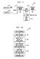
- FIG. 2is a block diagram depicting an exemplary random number generator circuit according to an embodiment of the invention.
- FIG. 3Adepicts steps in an exemplary method for programming the error code memory shown in FIG. 2 , in accordance with an embodiment of the invention.
- FIG. 3Bdepicts steps in an exemplary method for recalling a corrected random number, in accordance with an embodiment of the invention.
- FIG. 4is a partial sectional view depicting an exemplary packaged IC comprising at least one secure random number generator circuit according to an embodiment of the present invention.
- embodiments of the inventionmay be fabricated in a silicon wafer, embodiments of the invention can alternatively be fabricated in wafers comprising other materials, including but not limited to gallium arsenide (GaAs), indium phosphide (InP), etc.
- GaAsgallium arsenide
- InPindium phosphide
- FIG. 1is a schematic diagram depicting an exemplary SRAM array 18 which may be used in conjunction with an embodiment of the invention.
- SRAM array 18includes a plurality of SRAM cells 20 arranged in an array of N rows and M columns, where N and M are integers, with a cell residing at each intersection of a row and a column.
- SRAM cells 20 corresponding to a given row in SRAM array 18are preferably connected to a common row line (e.g., Row 0 or Row N), also referred to as a word line.
- SRAM cells 20 corresponding to a given columnare connected to a common pair of complementary column lines (e.g., Column 0 and ColumnC 0 , or Column M and ColumnC M), also referred to as bit lines. In each pair of column lines, ColumnC represents a logical complement of Column.
- Each SRAM cell 20is preferably a six-transistor cell, comprising two n-channel metal-oxide-semiconductor (NMOS) pull-down transistor devices 40 and 42 , two p-channel metal-oxide-semiconductor (PMOS) pull-up transistor devices 46 and 48 , and two NMOS access transistor devices 30 and 32 .
- the inventionis not limited to the specific memory cell configuration shown.
- sources of devices 46 and 48are connected together and are adapted for connection to a first voltage supply, which may be VDD; a drain of device 46 is connected to a drain of device 40 at node 34 ; sources of devices 40 and 42 are connected together and are adapted for connection to a second voltage supply, which may be ground; a drain of device 42 is connected to a drain of device 48 at node 36 ; gates of devices 46 and 40 are connected to the drains of devices 48 and 42 at node 36 ; and gates of devices 48 and 42 are connected to the drains of devices 46 and 40 at node 34 .
- a first voltage supplywhich may be VDD
- a drain of device 46is connected to a drain of device 40 at node 34
- sources of devices 40 and 42are connected together and are adapted for connection to a second voltage supply, which may be ground
- a drain of device 42is connected to a drain of device 48 at node 36
- gates of devices 46 and 40are connected to the drains of devices 48 and 42 at node 36
- a drain of access transistor 30is connected to node 34 ; a drain of access device 32 is connected to node 36 ; a source of device 30 is adapted for connection to a corresponding column line (e.g., Column 0 ); a source of device 32 is adapted for connection to a corresponding complement column line (e.g., ColumnC 0 ); and gates of devices 30 and 32 are connected to a corresponding row line (e.g., Row 0 ).
- SRAM cells 20may be arranged in an array, as shown in FIG. 1 .
- SRAM cells 20may be arranged in a single row (not shown), in which case the cells may all be accessed in a single memory read cycle.
- the column linesare preferably oriented in a substantially vertical dimension and the row lines are preferably oriented in a substantially horizontal dimension, such that the row and column lines are substantially orthogonal relative to one another. It is to be understood, however, that the invention is not limited to any specific arrangement of the memory cells and/or orientation of the row and column lines. For example, other orientations of the row and column lines (e.g., diagonal) are similarly contemplated and are within the scope of the present invention.
- a typical memory cellWhen first powered up, a typical memory cell may be in one of two stable initial states, namely, a first state indicative of a logic high level (e.g., binary “1”), which may be VDD (e.g., about 3.3 volts), or a second state indicative of a logic low level (e.g., binary “0”), which may be zero volts.
- the term initial stateis intended to be defined as the data state that the memory cell is in immediately after it is powered up and before it is written to.
- an SRAM cellis designed to be a symmetrical and balanced circuit, thus the SRAM cell has an equal probability of being in an initial state of binary 1 or binary 0 when powered up.
- the initial state of a given memory cellis determined primarily by process variations and fluctuations. As with any physical structures, there are typically variations in dimensions, component concentrations and other physical properties.
- one or more variations in certain characteristics associated with transistors forming a given memory cellcan occur, including, for example, doping levels within transistor source and drain regions, doping level within a transistor channel region, transistor gate oxide capacitance, trapped charge within transistor gate oxide, trapped charge within the transistor channel region, geometrical offsets between transistor regions, transistor channel length and transistor channel width, etc. Additionally, variations can occur in, for example, interconnect thickness, length and width, and in resistances and capacitances within the memory cell. These variations in physical and/or process parameters associated with the memory cells are predominantly random, and thus, for each memory cell, the binary state that is achieved in the cell after being powered up is essentially random.
- memory cells suitable for use with the present inventionmay comprise any circuit elements that can have initial states set by non-programmed process and/or dimensional variations.
- Such memory cellsmay include, but are not limited to, flip-flops, latches, the illustrative SRAM cell type shown in FIG. 1 , other SRAM cell types, other complimentary metal-oxide-semiconductor (CMOS) circuit elements, etc.
- CMOScomplimentary metal-oxide-semiconductor
- SRAM cells in a memory arraywill have a large enough composite imbalance due to variations in process and/or dimensional characteristics associated with the cells to cause a repeatable initial state, hereinafter referred to as a definite initial state.
- a definite initial stateIn this instance, every time a memory cell is powered up, its initial state will always be the same; always a binary 0 state or always a binary 1 state.
- Memory cells exhibiting a non-repeatable initial statemay be influenced by other, time variant, variables such as, but not limited to, chip temperature, supply voltage level, supply voltage slew rate and electrical noise (e.g., switching noise, cross-talk, etc.) in the vicinity of the cell.
- variablessuch as, but not limited to, chip temperature, supply voltage level, supply voltage slew rate and electrical noise (e.g., switching noise, cross-talk, etc.) in the vicinity of the cell.
- error correction techniquesare advantageously employed to define the states of memory cells having indefinite initial states.
- ECCserror correction codes
- One of the simpler forms of ECCis based upon block codes.
- a widely used block codeis a Hamming code.
- Reed-Soloman (RS) and Bose-Chaudhuri-Hocquenghem (BCH) codesare other known error correction codes.
- Methods of error correctionare well known in the art (see, e.g., Roberto Togneri and Christopher J. S. deSilva, “Fundamentals of Information Theory and Coding Design,” Chapman & Hall/CRC Press, 2002).
- FIG. 2is a block diagram depicting an exemplary random number generator circuit 200 according to an embodiment of the present invention.
- Random number generator circuit 200comprises a first memory 201 , which may be an SRAM memory array, including a plurality of memory cells, or alternative storage elements.
- Memory 201is adapted for connection to a power supply 202 operative to supply a source of voltage, which may be VDD, to the memory.
- Memory 201is preferably nonvolatile and is operative to generate, as an output, a first signal 206 , which may be an uncorrected random number, which is a function of respective initial states of the plurality of memory cells in the memory.
- SRAMis not considered to be nonvolatile memory since, as it is conventionally used, data stored in the SRAM is lost when power to the memory is removed (i.e., when the SRAM is powered down).
- SRAMis employed as a nonvolatile storage medium for purposes of generating a secure random number, since at least a portion of the memory cells in the SRAM will have the same (i.e., repeatable) initial state each and every time the memory is powered up.
- the memory cells in memory 201may be arranged, for example, in an N-by-M array, wherein N and M are both integers.
- the inventionis not limited to any particular size and/or arrangement of the memory cells in memory 201 .
- memory 201may comprise an array of 16 words by 32 bits (16-by-32 array). This arrangement requires 16 memory read cycles, each read cycle generating one 32-bit data word, to produce 512 bits of data.
- Random number generator circuit 200may include a controller 205 coupled to memory 201 for controlling access to the memory cells in the memory.
- controller 205may comprise row and/or column related circuitry, as will be known by those skilled in the art.
- the memory cells in memory 201may be arranged in a single row of M cells (e.g., a 1-by-M array).
- memory 201may comprise M individual latches (not explicitly shown) functioning in parallel.
- the entire row of M memory cellsmay be read concurrently within a single memory read cycle.
- controller 205may be eliminated.
- this arrangementwould require a considerably greater number of sense amplifiers for simultaneously reading the states of the memory cells, which may increase the overall area and cost of the IC.
- Data wordsare preferably read from memory 201 after the memory has been powered up (e.g., at a prescribed time after VDD is applied to the memory) and after an initial state of the memory has been established.
- Reading memory 201preferably enables a transfer of data words, upon which the uncorrected random number 206 is based, from the memory to subsequent processing circuitry in the random number generator circuit 200 .
- Random number generator circuit 200further includes an error correction circuit 203 coupled to memory 201 .
- Error correction circuit 203is preferably operative to correct data words generated by memory cells having indefinite initial states such that all data bits read from memory 201 will be definite (repeatable).
- a second signal 207which may be a corrected random number, generated by error correction circuit 203 will be random but repeatable.
- the output security code generated by the random number generator circuit 200is preferably a function of the corrected random number 207 .
- a second memory 204which may be an error code memory, may be optionally coupled to the error correction circuit.
- Memory 204is preferably nonvolatile and is operative to store ECC bits used by the error correction methodology. These ECC bits are preferably programmed into memory 204 at some point in time when the security code (random number) is being established. This may be during or shortly after device factory or customer test. These ECC bits need only be programmed once, although they could be reprogrammed at a later time if it is desired to reset the security code.
- memory 204is programmed by initially powering up memory 201 and storing the initial states of the memory cells in memory 201 at the timing of programming. These programmed states are considered to be the “correct” state of memory 201 . During subsequent power-up, the initial states of the memory cells in memory 201 will be compared to the “correct” state stored in memory 204 and any indefinite bits not matching the stored states will be corrected by error correction circuit 203 .
- error correction circuit 203may employ, for example, a block code (e.g., a Hamming code), a RS code, a BCH code, etc., in generating the corrected random number 207 , although the invention is not limited to a particular error correction methodology.
- a block codee.g., a Hamming code
- RS codee.g., a RS code
- BCH codee.g., a BCH code
- Certain error correction techniqueshave limitations on the number and/or arrangement of correctable bits. For example, Hamming codes, while simple to implement, can only correct one bit error per data word.
- Hamming codesare therefore preferred where the number of bits in a given data word is relatively small (e.g., less than about 16 bits).
- Other error correction techniques employed by error correction circuit 203may not require storage of a memory code, and consequently memory 204 may be omitted.
- Method 300for programming the illustrative error code memory 204 of FIG. 2 is shown, in accordance with an embodiment of the invention.
- Method 300at least a portion of which may be performed in error correction circuit 203 , can be used to set the “correct” state of the memory cells in memory 201 having indefinite initial states (see FIG. 2 ). In this manner, method 300 is preferably employed to correct non-repeatable bits in the uncorrected random number 206 generated from memory 201 .
- non-repeatable bitis intended to refer broadly to an output of a given memory cell in memory 201 that does not have a consistent initial state, such that upon successive applications of power to the memory, the initial state of the given memory cell may not necessarily be the same as the initial state of the given cell during one or more previous applications of power to the cell.
- step 302memory 201 is first powered up in step 302 .
- step 303memory 201 is read to generate a first random number, based on uncorrected random number 206 , which is forwarded to error correction circuit 203 .
- This first random numbermay include bits that are non-repeatable.
- step 304error correction circuit 203 generates an error correction code 208 that is representative of the first random number.
- step 305the error correction code 208 is programmed into error code memory 204 .
- the error correction code 208may be a Hamming code for each data word read from memory 201 .
- corrected random number 207 generated by error correction circuit 203will be random but repeatable.
- FIG. 3Bdepicts steps in an exemplary method 320 for recalling a corrected random number (e.g., 207 in FIG. 2 ), in accordance with an embodiment of the invention.
- Recallis preferably performed after error code memory 204 has been programmed, for example using exemplary method 300 depicted in FIG. 3A .
- Method 320begins by powering up memory 201 in step 322 . During power up, the initial states of all the bits in the uncorrected dataword are established. In step 323 , a second random number is generated based on the uncorrected random number 206 read from memory 201 . Because of non-repeatable bits, the second random number may be different from the first random number generated during the error code memory programming method 300 described above in conjunction with FIG.
- step 324the error correction code 208 is read from error code memory 204 .
- this error correction code 208any non-repeatable bits in the second random number having states that do not match corresponding states in the first random number, as indicated by the stored error correction code, are corrected in step 325 .
- the corrected random number 207will be generated from the second random number. This will be the same number as the first random number generated during the programming method 300 . If, in step 323 , it is determined that the second random is the same as the first random number generated in method 300 , correction need not be performed. In this instance, steps 324 and 325 may be omitted.
- FIG. 4is a partial sectional view depicting an exemplary packaged IC 400 comprising at least one secure random number generator according to an embodiment of the present invention.
- the packaged IC 400comprises a leadframe 402 , a die 404 attached to the leadframe, the die including a secure random number generator in accordance with an embodiment of the invention, and a plastic encapsulation mold 608 .
- One skilled in the artwould know how to dice wafers and package die to produce integrated circuits. Integrated circuits so manufactured are considered part of this invention.
- An integrated circuit in accordance with the present inventioncan be employed in any application and/or electronic system which utilizes security codes.
- Suitable systems for implementing the inventionmay include, but are not limited to, personal computers, communication networks, electronic commerce systems, portable communications devices (e.g., cell phones), solid-state media storage devices, etc. Systems incorporating such integrated circuits are considered part of this invention. Given the teachings of the invention provided herein, one of ordinary skill in the art will be able to contemplate other implementations and applications of the techniques of the invention.
Landscapes
- Engineering & Computer Science (AREA)
- Theoretical Computer Science (AREA)
- Physics & Mathematics (AREA)
- General Physics & Mathematics (AREA)
- Microelectronics & Electronic Packaging (AREA)
- General Engineering & Computer Science (AREA)
- Mathematical Optimization (AREA)
- Mathematical Analysis (AREA)
- Computational Mathematics (AREA)
- Pure & Applied Mathematics (AREA)
- Quality & Reliability (AREA)
- Computer Hardware Design (AREA)
- Semiconductor Memories (AREA)
- For Increasing The Reliability Of Semiconductor Memories (AREA)
- Semiconductor Integrated Circuits (AREA)
- Techniques For Improving Reliability Of Storages (AREA)
Abstract
Description
Claims (20)
Applications Claiming Priority (1)
| Application Number | Priority Date | Filing Date | Title |
|---|---|---|---|
| PCT/US2008/064679WO2009142645A1 (en) | 2008-05-23 | 2008-05-23 | Secure random number generator |
Publications (2)
| Publication Number | Publication Date |
|---|---|
| US20110022648A1 US20110022648A1 (en) | 2011-01-27 |
| US8566377B2true US8566377B2 (en) | 2013-10-22 |
Family
ID=40083710
Family Applications (1)
| Application Number | Title | Priority Date | Filing Date |
|---|---|---|---|
| US12/934,510Expired - Fee RelatedUS8566377B2 (en) | 2008-05-23 | 2008-05-23 | Secure random number generator |
Country Status (7)
| Country | Link |
|---|---|
| US (1) | US8566377B2 (en) |
| EP (1) | EP2300909B1 (en) |
| JP (1) | JP5279899B2 (en) |
| KR (1) | KR101374427B1 (en) |
| CN (1) | CN102037441A (en) |
| TW (1) | TWI435586B (en) |
| WO (1) | WO2009142645A1 (en) |
Cited By (9)
| Publication number | Priority date | Publication date | Assignee | Title |
|---|---|---|---|---|
| US9529570B2 (en) | 2014-03-19 | 2016-12-27 | Seagate Technology Llc | Random number generation using pulsed programming parameters |
| US9971565B2 (en) | 2015-05-07 | 2018-05-15 | Oracle International Corporation | Storage, access, and management of random numbers generated by a central random number generator and dispensed to hardware threads of cores |
| US9984256B2 (en) | 2014-05-15 | 2018-05-29 | Seagate Technology Llc | Storage device tampering detection |
| US10116441B1 (en) | 2015-06-11 | 2018-10-30 | Amazon Technologies, Inc. | Enhanced-security random data |
| US10338890B1 (en) | 2015-01-07 | 2019-07-02 | Seagate Technology Llc | Random values from data errors |
| US10372528B1 (en) | 2014-12-15 | 2019-08-06 | Seagate Technology Llc | Random values from data errors |
| US10536266B2 (en) | 2017-05-02 | 2020-01-14 | Seagate Technology Llc | Cryptographically securing entropy for later use |
| US11055229B2 (en) | 2018-11-22 | 2021-07-06 | Samsung Electronics Co., Ltd. | Memory controller including address translation module, memory system including the memory controller, and operating method of the memory controller |
| US11709656B2 (en) | 2018-07-13 | 2023-07-25 | Ememory Technology Inc. | Short channel effect based random bit generator |
Families Citing this family (57)
| Publication number | Priority date | Publication date | Assignee | Title |
|---|---|---|---|---|
| JP5279899B2 (en) | 2008-05-23 | 2013-09-04 | アギア システムズ インコーポレーテッド | Secure random number generator |
| WO2010134197A1 (en)* | 2009-05-22 | 2010-11-25 | 株式会社 東芝 | Random number generation circuit and encryption circuit using the same |
| TWI496075B (en)* | 2010-06-03 | 2015-08-11 | Univ Michigan | Randomized value generation |
| US9224496B2 (en) | 2010-08-11 | 2015-12-29 | Shine C. Chung | Circuit and system of aggregated area anti-fuse in CMOS processes |
| US9496033B2 (en) | 2010-08-20 | 2016-11-15 | Attopsemi Technology Co., Ltd | Method and system of programmable resistive devices with read capability using a low supply voltage |
| US9236141B2 (en) | 2010-08-20 | 2016-01-12 | Shine C. Chung | Circuit and system of using junction diode of MOS as program selector for programmable resistive devices |
| US9042153B2 (en) | 2010-08-20 | 2015-05-26 | Shine C. Chung | Programmable resistive memory unit with multiple cells to improve yield and reliability |
| US10229746B2 (en) | 2010-08-20 | 2019-03-12 | Attopsemi Technology Co., Ltd | OTP memory with high data security |
| US9251893B2 (en) | 2010-08-20 | 2016-02-02 | Shine C. Chung | Multiple-bit programmable resistive memory using diode as program selector |
| US10916317B2 (en) | 2010-08-20 | 2021-02-09 | Attopsemi Technology Co., Ltd | Programmable resistance memory on thin film transistor technology |
| US9818478B2 (en) | 2012-12-07 | 2017-11-14 | Attopsemi Technology Co., Ltd | Programmable resistive device and memory using diode as selector |
| US9025357B2 (en) | 2010-08-20 | 2015-05-05 | Shine C. Chung | Programmable resistive memory unit with data and reference cells |
| US9460807B2 (en) | 2010-08-20 | 2016-10-04 | Shine C. Chung | One-time programmable memory devices using FinFET technology |
| US9824768B2 (en) | 2015-03-22 | 2017-11-21 | Attopsemi Technology Co., Ltd | Integrated OTP memory for providing MTP memory |
| US10249379B2 (en) | 2010-08-20 | 2019-04-02 | Attopsemi Technology Co., Ltd | One-time programmable devices having program selector for electrical fuses with extended area |
| US10923204B2 (en) | 2010-08-20 | 2021-02-16 | Attopsemi Technology Co., Ltd | Fully testible OTP memory |
| US9711237B2 (en) | 2010-08-20 | 2017-07-18 | Attopsemi Technology Co., Ltd. | Method and structure for reliable electrical fuse programming |
| US8488364B2 (en) | 2010-08-20 | 2013-07-16 | Shine C. Chung | Circuit and system of using a polysilicon diode as program selector for resistive devices in CMOS logic processes |
| US9070437B2 (en) | 2010-08-20 | 2015-06-30 | Shine C. Chung | Circuit and system of using junction diode as program selector for one-time programmable devices with heat sink |
| US9431127B2 (en) | 2010-08-20 | 2016-08-30 | Shine C. Chung | Circuit and system of using junction diode as program selector for metal fuses for one-time programmable devices |
| US9019742B2 (en) | 2010-08-20 | 2015-04-28 | Shine C. Chung | Multiple-state one-time programmable (OTP) memory to function as multi-time programmable (MTP) memory |
| US8988965B2 (en) | 2010-11-03 | 2015-03-24 | Shine C. Chung | Low-pin-count non-volatile memory interface |
| US9076513B2 (en) | 2010-11-03 | 2015-07-07 | Shine C. Chung | Low-pin-count non-volatile memory interface with soft programming capability |
| US9019791B2 (en) | 2010-11-03 | 2015-04-28 | Shine C. Chung | Low-pin-count non-volatile memory interface for 3D IC |
| US9496265B2 (en) | 2010-12-08 | 2016-11-15 | Attopsemi Technology Co., Ltd | Circuit and system of a high density anti-fuse |
| US8848423B2 (en) | 2011-02-14 | 2014-09-30 | Shine C. Chung | Circuit and system of using FinFET for building programmable resistive devices |
| US10586832B2 (en) | 2011-02-14 | 2020-03-10 | Attopsemi Technology Co., Ltd | One-time programmable devices using gate-all-around structures |
| US10192615B2 (en) | 2011-02-14 | 2019-01-29 | Attopsemi Technology Co., Ltd | One-time programmable devices having a semiconductor fin structure with a divided active region |
| EP2695052B1 (en)* | 2011-04-05 | 2014-11-26 | Intrinsic ID B.V. | Random number generating system based on memory start-up noise |
| JP5813380B2 (en)* | 2011-06-03 | 2015-11-17 | 株式会社東芝 | Semiconductor memory device |
| US9324849B2 (en) | 2011-11-15 | 2016-04-26 | Shine C. Chung | Structures and techniques for using semiconductor body to construct SCR, DIAC, or TRIAC |
| US9136261B2 (en) | 2011-11-15 | 2015-09-15 | Shine C. Chung | Structures and techniques for using mesh-structure diodes for electro-static discharge (ESD) protection |
| US9007804B2 (en)* | 2012-02-06 | 2015-04-14 | Shine C. Chung | Circuit and system of protective mechanisms for programmable resistive memories |
| US9076526B2 (en) | 2012-09-10 | 2015-07-07 | Shine C. Chung | OTP memories functioning as an MTP memory |
| US9183897B2 (en) | 2012-09-30 | 2015-11-10 | Shine C. Chung | Circuits and methods of a self-timed high speed SRAM |
| US20160028544A1 (en)* | 2012-11-15 | 2016-01-28 | Elwha Llc | Random number generator functions in memory |
| US9324447B2 (en) | 2012-11-20 | 2016-04-26 | Shine C. Chung | Circuit and system for concurrently programming multiple bits of OTP memory devices |
| JP6103958B2 (en)* | 2013-01-25 | 2017-03-29 | 株式会社メガチップス | Semiconductor memory device |
| US9201729B2 (en)* | 2013-10-21 | 2015-12-01 | Seagate Technology, Llc | Systems and methods for soft data utilization in a solid state memory system |
| US9412473B2 (en) | 2014-06-16 | 2016-08-09 | Shine C. Chung | System and method of a novel redundancy scheme for OTP |
| JP6587188B2 (en) | 2015-06-18 | 2019-10-09 | パナソニックIpマネジメント株式会社 | Random number processing apparatus, integrated circuit card, and random number processing method |
| KR20170008546A (en)* | 2015-07-14 | 2017-01-24 | 에스케이하이닉스 주식회사 | Random number generation circuit and semiconductor system using the same |
| US9747982B1 (en) | 2016-02-22 | 2017-08-29 | Arm Ltd. | Device and method for generating random numbers |
| US10910079B2 (en)* | 2016-05-09 | 2021-02-02 | Intrinsic Id B.V. | Programming device arranged to obtain and store a random bit string in a memory device |
| US10019236B2 (en) | 2016-08-11 | 2018-07-10 | Taiwan Semiconductor Manufacturing Co., Ltd. | SRAM-based true random number generator |
| US10535413B2 (en) | 2017-04-14 | 2020-01-14 | Attopsemi Technology Co., Ltd | Low power read operation for programmable resistive memories |
| US11062786B2 (en) | 2017-04-14 | 2021-07-13 | Attopsemi Technology Co., Ltd | One-time programmable memories with low power read operation and novel sensing scheme |
| US11615859B2 (en) | 2017-04-14 | 2023-03-28 | Attopsemi Technology Co., Ltd | One-time programmable memories with ultra-low power read operation and novel sensing scheme |
| US10726914B2 (en) | 2017-04-14 | 2020-07-28 | Attopsemi Technology Co. Ltd | Programmable resistive memories with low power read operation and novel sensing scheme |
| US10090309B1 (en)* | 2017-04-27 | 2018-10-02 | Ememory Technology Inc. | Nonvolatile memory cell capable of improving program performance |
| US10770160B2 (en) | 2017-11-30 | 2020-09-08 | Attopsemi Technology Co., Ltd | Programmable resistive memory formed by bit slices from a standard cell library |
| KR102045764B1 (en)* | 2018-02-02 | 2019-11-18 | 안상욱 | Sram cell for generating true random number and sram cell arry driving circuit using the same |
| US10880101B2 (en) | 2018-04-11 | 2020-12-29 | Taiwan Semiconductor Manufacturing Co., Ltd. | Method and circuit for de-biasing PUF bits |
| KR102155007B1 (en)* | 2019-02-14 | 2020-09-11 | 국민대학교산학협력단 | Entropy management apparatus and method using independence measurement, and number generation apparatus using the same |
| KR102197744B1 (en) | 2020-02-04 | 2021-01-04 | 금오공과대학교 산학협력단 | True random number generator based on cellular automata with random transition rules |
| US11049555B1 (en)* | 2020-05-08 | 2021-06-29 | Taiwan Semiconductor Manufacturing Company, Ltd. | SRAM power-up random number generator |
| US11562784B2 (en)* | 2020-08-14 | 2023-01-24 | Micron Technology, Inc. | Apparatuses, systems, and methods for voltage based random number generation |
Citations (5)
| Publication number | Priority date | Publication date | Assignee | Title |
|---|---|---|---|---|
| US20040062084A1 (en) | 2002-09-30 | 2004-04-01 | Layman Paul Arthur | Electronic fingerprinting of semiconductor integrated circuits |
| US20050076274A1 (en) | 2003-10-03 | 2005-04-07 | Takeshi Nagai | Semiconductor integrated circuit |
| US20050144430A1 (en) | 2003-12-25 | 2005-06-30 | Matsushita Electric Industrial Co., Ltd. | Information processing apparatus and a ROM image generation apparatus for the apparatus |
| US20090049111A1 (en)* | 2004-11-12 | 2009-02-19 | Suresh Narayana Chari | Method, apparatus and system for resistance to side channel attacks on random number generators |
| WO2009142645A1 (en) | 2008-05-23 | 2009-11-26 | Agere Systems Inc. | Secure random number generator |
Family Cites Families (1)
| Publication number | Priority date | Publication date | Assignee | Title |
|---|---|---|---|---|
| JP4251564B2 (en)* | 2004-10-08 | 2009-04-08 | 株式会社リコー | Image forming apparatus |
- 2008
- 2008-05-23JPJP2011510477Apatent/JP5279899B2/ennot_activeExpired - Fee Related
- 2008-05-23USUS12/934,510patent/US8566377B2/ennot_activeExpired - Fee Related
- 2008-05-23EPEP08756186.6Apatent/EP2300909B1/ennot_activeNot-in-force
- 2008-05-23KRKR1020107026047Apatent/KR101374427B1/ennot_activeExpired - Fee Related
- 2008-05-23CNCN2008801293958Apatent/CN102037441A/enactivePending
- 2008-05-23WOPCT/US2008/064679patent/WO2009142645A1/enactiveApplication Filing
- 2008-12-25TWTW097150722Apatent/TWI435586B/ennot_activeIP Right Cessation
Patent Citations (13)
| Publication number | Priority date | Publication date | Assignee | Title |
|---|---|---|---|---|
| US20040062084A1 (en) | 2002-09-30 | 2004-04-01 | Layman Paul Arthur | Electronic fingerprinting of semiconductor integrated circuits |
| US7266025B2 (en) | 2003-10-03 | 2007-09-04 | Kabushiki Kaisha Toshiba | Semiconductor integrated circuit |
| US20050076274A1 (en) | 2003-10-03 | 2005-04-07 | Takeshi Nagai | Semiconductor integrated circuit |
| JP2005116003A (en) | 2003-10-03 | 2005-04-28 | Toshiba Corp | Semiconductor integrated circuit |
| US7308567B2 (en) | 2003-12-25 | 2007-12-11 | Matsushita Electric Industrial Co., Ltd. | Information processing apparatus for performing a system boot by using programs stored in a non-voltile storage device |
| JP2005190201A (en) | 2003-12-25 | 2005-07-14 | Matsushita Electric Ind Co Ltd | Information processor and rom image generation device for the same |
| US20050144430A1 (en) | 2003-12-25 | 2005-06-30 | Matsushita Electric Industrial Co., Ltd. | Information processing apparatus and a ROM image generation apparatus for the apparatus |
| US20080082860A1 (en) | 2003-12-25 | 2008-04-03 | Matsushita Electric Industrial Co., Ltd. | Information processing apparatus for performing a system boot by using programs stored in a non-volatile storage device |
| CN101183313A (en) | 2003-12-25 | 2008-05-21 | 松下电器产业株式会社 | Information processing device and ROM image generating device for the device |
| US7925928B2 (en) | 2003-12-25 | 2011-04-12 | Panasonic Corporation | Information processing apparatus for performing a system boot by using programs stored in a non-volatile storage device |
| US20090049111A1 (en)* | 2004-11-12 | 2009-02-19 | Suresh Narayana Chari | Method, apparatus and system for resistance to side channel attacks on random number generators |
| WO2009142645A1 (en) | 2008-05-23 | 2009-11-26 | Agere Systems Inc. | Secure random number generator |
| US20110022648A1 (en)* | 2008-05-23 | 2011-01-27 | Harris Edward B | Secure Random Number Generator |
Cited By (10)
| Publication number | Priority date | Publication date | Assignee | Title |
|---|---|---|---|---|
| US9529570B2 (en) | 2014-03-19 | 2016-12-27 | Seagate Technology Llc | Random number generation using pulsed programming parameters |
| US9984256B2 (en) | 2014-05-15 | 2018-05-29 | Seagate Technology Llc | Storage device tampering detection |
| US10372528B1 (en) | 2014-12-15 | 2019-08-06 | Seagate Technology Llc | Random values from data errors |
| US10338890B1 (en) | 2015-01-07 | 2019-07-02 | Seagate Technology Llc | Random values from data errors |
| US9971565B2 (en) | 2015-05-07 | 2018-05-15 | Oracle International Corporation | Storage, access, and management of random numbers generated by a central random number generator and dispensed to hardware threads of cores |
| US10116441B1 (en) | 2015-06-11 | 2018-10-30 | Amazon Technologies, Inc. | Enhanced-security random data |
| US10536266B2 (en) | 2017-05-02 | 2020-01-14 | Seagate Technology Llc | Cryptographically securing entropy for later use |
| US11709656B2 (en) | 2018-07-13 | 2023-07-25 | Ememory Technology Inc. | Short channel effect based random bit generator |
| US11989533B2 (en) | 2018-07-13 | 2024-05-21 | Ememory Technology Inc. | Short channel effect based random bit generator |
| US11055229B2 (en) | 2018-11-22 | 2021-07-06 | Samsung Electronics Co., Ltd. | Memory controller including address translation module, memory system including the memory controller, and operating method of the memory controller |
Also Published As
| Publication number | Publication date |
|---|---|
| CN102037441A (en) | 2011-04-27 |
| JP5279899B2 (en) | 2013-09-04 |
| TWI435586B (en) | 2014-04-21 |
| WO2009142645A1 (en) | 2009-11-26 |
| TW200950455A (en) | 2009-12-01 |
| US20110022648A1 (en) | 2011-01-27 |
| EP2300909B1 (en) | 2015-04-15 |
| JP2011521376A (en) | 2011-07-21 |
| KR20110010733A (en) | 2011-02-07 |
| KR101374427B1 (en) | 2014-03-17 |
| EP2300909A1 (en) | 2011-03-30 |
Similar Documents
| Publication | Publication Date | Title |
|---|---|---|
| US8566377B2 (en) | Secure random number generator | |
| TWI707358B (en) | Physical unclonable function using twin-cell charge trap transistor memory | |
| JP7724898B2 (en) | Anti-hacking mechanism for flash memory devices | |
| US10880103B2 (en) | SRAM-based authentication circuit | |
| US8854866B2 (en) | Identification circuit and method for generating an identification bit | |
| US8767445B2 (en) | SRAM circuits for circuit identification using a digital fingerprint | |
| US8896978B2 (en) | Integrated circuit with automatic deactivation upon exceeding a specific ion linear energy transfer (LET) value | |
| TW201926113A (en) | Method of generating security key for integrated circuit device | |
| US8468419B2 (en) | High-reliability memory | |
| US10657294B2 (en) | Non-volatile memory with physical unclonable function | |
| US6738294B2 (en) | Electronic fingerprinting of semiconductor integrated circuits | |
| TW201944279A (en) | Method and circuit for de-biasing PUF bits | |
| US20220385486A1 (en) | Physically unclonable function produced using otp memory | |
| US9941886B2 (en) | Integrated circuit (IC) chip comprising an identification circuit | |
| Li et al. | Reliable antifuse one-time-programmable scheme with charge pump for postpackage repair of DRAM | |
| Serrano et al. | A Unified OTP and PUF Exploiting Post-Program Current on Standard CMOS Technology | |
| US8165291B2 (en) | Random seed stability with fuses | |
| US7676726B2 (en) | Stabilization for random chip identifier circuit |
Legal Events
| Date | Code | Title | Description |
|---|---|---|---|
| AS | Assignment | Owner name:AGERE SYSTEMS INC., PENNSYLVANIA Free format text:ASSIGNMENT OF ASSIGNORS INTEREST;ASSIGNORS:HARRIS, EDWARD B.;HOGG, RICHARD;KOHLER, ROSS A.;AND OTHERS;REEL/FRAME:025040/0939 Effective date:20080521 | |
| AS | Assignment | Owner name:AGERE SYSTEMS LLC, PENNSYLVANIA Free format text:CERTIFICATE OF CONVERSION;ASSIGNOR:AGERE SYSTEMS INC.;REEL/FRAME:031248/0549 Effective date:20120730 | |
| STCF | Information on status: patent grant | Free format text:PATENTED CASE | |
| AS | Assignment | Owner name:DEUTSCHE BANK AG NEW YORK BRANCH, AS COLLATERAL AG Free format text:PATENT SECURITY AGREEMENT;ASSIGNORS:LSI CORPORATION;AGERE SYSTEMS LLC;REEL/FRAME:032856/0031 Effective date:20140506 | |
| AS | Assignment | Owner name:AVAGO TECHNOLOGIES GENERAL IP (SINGAPORE) PTE. LTD Free format text:ASSIGNMENT OF ASSIGNORS INTEREST;ASSIGNOR:AGERE SYSTEMS LLC;REEL/FRAME:035365/0634 Effective date:20140804 | |
| AS | Assignment | Owner name:LSI CORPORATION, CALIFORNIA Free format text:TERMINATION AND RELEASE OF SECURITY INTEREST IN PATENT RIGHTS (RELEASES RF 032856-0031);ASSIGNOR:DEUTSCHE BANK AG NEW YORK BRANCH, AS COLLATERAL AGENT;REEL/FRAME:037684/0039 Effective date:20160201 Owner name:AGERE SYSTEMS LLC, PENNSYLVANIA Free format text:TERMINATION AND RELEASE OF SECURITY INTEREST IN PATENT RIGHTS (RELEASES RF 032856-0031);ASSIGNOR:DEUTSCHE BANK AG NEW YORK BRANCH, AS COLLATERAL AGENT;REEL/FRAME:037684/0039 Effective date:20160201 | |
| AS | Assignment | Owner name:BANK OF AMERICA, N.A., AS COLLATERAL AGENT, NORTH CAROLINA Free format text:PATENT SECURITY AGREEMENT;ASSIGNOR:AVAGO TECHNOLOGIES GENERAL IP (SINGAPORE) PTE. LTD.;REEL/FRAME:037808/0001 Effective date:20160201 Owner name:BANK OF AMERICA, N.A., AS COLLATERAL AGENT, NORTH Free format text:PATENT SECURITY AGREEMENT;ASSIGNOR:AVAGO TECHNOLOGIES GENERAL IP (SINGAPORE) PTE. LTD.;REEL/FRAME:037808/0001 Effective date:20160201 | |
| AS | Assignment | Owner name:AVAGO TECHNOLOGIES GENERAL IP (SINGAPORE) PTE. LTD., SINGAPORE Free format text:TERMINATION AND RELEASE OF SECURITY INTEREST IN PATENTS;ASSIGNOR:BANK OF AMERICA, N.A., AS COLLATERAL AGENT;REEL/FRAME:041710/0001 Effective date:20170119 Owner name:AVAGO TECHNOLOGIES GENERAL IP (SINGAPORE) PTE. LTD Free format text:TERMINATION AND RELEASE OF SECURITY INTEREST IN PATENTS;ASSIGNOR:BANK OF AMERICA, N.A., AS COLLATERAL AGENT;REEL/FRAME:041710/0001 Effective date:20170119 | |
| FPAY | Fee payment | Year of fee payment:4 | |
| AS | Assignment | Owner name:AVAGO TECHNOLOGIES INTERNATIONAL SALES PTE. LIMITE Free format text:MERGER;ASSIGNOR:AVAGO TECHNOLOGIES GENERAL IP (SINGAPORE) PTE. LTD.;REEL/FRAME:047230/0910 Effective date:20180509 | |
| AS | Assignment | Owner name:AVAGO TECHNOLOGIES INTERNATIONAL SALES PTE. LIMITE Free format text:CORRECTIVE ASSIGNMENT TO CORRECT THE EFFECTIVE DATE OF THE MERGER PREVIOUSLY RECORDED AT REEL: 047230 FRAME: 0910. ASSIGNOR(S) HEREBY CONFIRMS THE MERGER;ASSIGNOR:AVAGO TECHNOLOGIES GENERAL IP (SINGAPORE) PTE. LTD.;REEL/FRAME:047351/0384 Effective date:20180905 | |
| AS | Assignment | Owner name:AVAGO TECHNOLOGIES INTERNATIONAL SALES PTE. LIMITE Free format text:CORRECTIVE ASSIGNMENT TO CORRECT THE ERROR IN RECORDING THE MERGER IN THE INCORRECT US PATENT NO. 8,876,094 PREVIOUSLY RECORDED ON REEL 047351 FRAME 0384. ASSIGNOR(S) HEREBY CONFIRMS THE MERGER;ASSIGNOR:AVAGO TECHNOLOGIES GENERAL IP (SINGAPORE) PTE. LTD.;REEL/FRAME:049248/0558 Effective date:20180905 | |
| FEPP | Fee payment procedure | Free format text:MAINTENANCE FEE REMINDER MAILED (ORIGINAL EVENT CODE: REM.); ENTITY STATUS OF PATENT OWNER: LARGE ENTITY | |
| LAPS | Lapse for failure to pay maintenance fees | Free format text:PATENT EXPIRED FOR FAILURE TO PAY MAINTENANCE FEES (ORIGINAL EVENT CODE: EXP.); ENTITY STATUS OF PATENT OWNER: LARGE ENTITY | |
| STCH | Information on status: patent discontinuation | Free format text:PATENT EXPIRED DUE TO NONPAYMENT OF MAINTENANCE FEES UNDER 37 CFR 1.362 | |
| FP | Lapsed due to failure to pay maintenance fee | Effective date:20211022 |