US8564897B1 - Systems and methods for enhanced sync mark detection - Google Patents
Systems and methods for enhanced sync mark detectionDownload PDFInfo
- Publication number
- US8564897B1 US8564897B1US13/529,572US201213529572AUS8564897B1US 8564897 B1US8564897 B1US 8564897B1US 201213529572 AUS201213529572 AUS 201213529572AUS 8564897 B1US8564897 B1US 8564897B1
- Authority
- US
- United States
- Prior art keywords
- sync
- sync mark
- ratio
- data
- pattern
- Prior art date
- Legal status (The legal status is an assumption and is not a legal conclusion. Google has not performed a legal analysis and makes no representation as to the accuracy of the status listed.)
- Active
Links
- 238000000034methodMethods0.000titleclaimsabstractdescription47
- 238000001514detection methodMethods0.000titleclaimsdescription42
- 238000012545processingMethods0.000claimsabstractdescription43
- 238000004364calculation methodMethods0.000claimsdescription30
- 230000008569processEffects0.000claimsdescription11
- 238000004891communicationMethods0.000claimsdescription7
- 230000003111delayed effectEffects0.000description24
- 238000009432framingMethods0.000description22
- 230000015654memoryEffects0.000description14
- 238000010586diagramMethods0.000description9
- 239000000523sampleSubstances0.000description7
- 230000005540biological transmissionEffects0.000description5
- 230000004044responseEffects0.000description4
- 239000012723sample bufferSubstances0.000description3
- 238000012546transferMethods0.000description3
- 238000012937correctionMethods0.000description2
- 238000005516engineering processMethods0.000description2
- 230000006870functionEffects0.000description2
- 239000013307optical fiberSubstances0.000description2
- RYGMFSIKBFXOCR-UHFFFAOYSA-NCopperChemical compound[Cu]RYGMFSIKBFXOCR-UHFFFAOYSA-N0.000description1
- 238000013459approachMethods0.000description1
- 230000001413cellular effectEffects0.000description1
- 238000006243chemical reactionMethods0.000description1
- 239000010949copperSubstances0.000description1
- 229910052802copperInorganic materials0.000description1
- 230000007547defectEffects0.000description1
- 230000002708enhancing effectEffects0.000description1
- 239000012634fragmentSubstances0.000description1
- 238000012986modificationMethods0.000description1
- 230000004048modificationEffects0.000description1
- 239000007787solidSubstances0.000description1
Images


Classifications
- G—PHYSICS
- G11—INFORMATION STORAGE
- G11B—INFORMATION STORAGE BASED ON RELATIVE MOVEMENT BETWEEN RECORD CARRIER AND TRANSDUCER
- G11B5/00—Recording by magnetisation or demagnetisation of a record carrier; Reproducing by magnetic means; Record carriers therefor
- G11B5/48—Disposition or mounting of heads or head supports relative to record carriers ; arrangements of heads, e.g. for scanning the record carrier to increase the relative speed
- G11B5/58—Disposition or mounting of heads or head supports relative to record carriers ; arrangements of heads, e.g. for scanning the record carrier to increase the relative speed with provision for moving the head for the purpose of maintaining alignment of the head relative to the record carrier during transducing operation, e.g. to compensate for surface irregularities of the latter or for track following
- G11B5/596—Disposition or mounting of heads or head supports relative to record carriers ; arrangements of heads, e.g. for scanning the record carrier to increase the relative speed with provision for moving the head for the purpose of maintaining alignment of the head relative to the record carrier during transducing operation, e.g. to compensate for surface irregularities of the latter or for track following for track following on disks
- G11B5/59688—Servo signal format patterns or signal processing thereof, e.g. dual, tri, quad, burst signal patterns
- G—PHYSICS
- G11—INFORMATION STORAGE
- G11B—INFORMATION STORAGE BASED ON RELATIVE MOVEMENT BETWEEN RECORD CARRIER AND TRANSDUCER
- G11B5/00—Recording by magnetisation or demagnetisation of a record carrier; Reproducing by magnetic means; Record carriers therefor
- G11B5/48—Disposition or mounting of heads or head supports relative to record carriers ; arrangements of heads, e.g. for scanning the record carrier to increase the relative speed
- G11B5/58—Disposition or mounting of heads or head supports relative to record carriers ; arrangements of heads, e.g. for scanning the record carrier to increase the relative speed with provision for moving the head for the purpose of maintaining alignment of the head relative to the record carrier during transducing operation, e.g. to compensate for surface irregularities of the latter or for track following
- G11B5/596—Disposition or mounting of heads or head supports relative to record carriers ; arrangements of heads, e.g. for scanning the record carrier to increase the relative speed with provision for moving the head for the purpose of maintaining alignment of the head relative to the record carrier during transducing operation, e.g. to compensate for surface irregularities of the latter or for track following for track following on disks
- G11B5/59605—Circuits
- G11B5/59616—Synchronisation; Clocking
Definitions
- the present inventionsare related to systems and methods for data processing, and more particularly to systems and methods for detecting patterns in a data stream.
- a synchronization markis identified based upon a threshold comparison.
- a threshold comparison approachdepends highly upon determining an appropriate threshold for comparison. Where the selected threshold is too high, sync marks will be missed. Alternatively, where the selected threshold is too low, sync marks may be incorrectly identified. Either case is problematic for proper data processing.
- the present inventionsare related to systems and methods for data processing, and more particularly to systems and methods for detecting patterns in a data stream.
- Various embodiments of the present inventionprovide data processing systems that include: a metric calculation circuit, a metric ratio calculation circuit, and a sync mark found circuit.
- the metric calculation circuitoperable to provide at least a first comparison value corresponding to a comparison between a received input data set and a sync mark pattern, and a second comparison value corresponding to a comparison between the received input data set and a subset of the sync mark pattern and a subset of a preamble pattern.
- the metric ratio calculation circuitoperable to calculate a first ratio of the first comparison value and the second comparison value, and a second ratio of the second comparison value and the third comparison value.
- the sync mark found circuitoperable to compare the first ratio with the second ratio, and to assert a sync found signal based at least in part on the result of the comparison of the first ratio with the second ratio.
- the aforementioned systemsare implemented as part of an integrated circuit.
- the systemsare implemented as part of a storage device or a wireless communication device.
- the sync mark patternis M bits in length
- the subset of the sync mark patternis N bits in length
- the subset of the preamble patternis M-N bits in length.
- Mis twenty
- Nmay be four, eight, twelve or sixteen.
- the sync mark pattern match calculation circuitis operable to process Y bits at a time
- the subset of the sync mark patternis one of the 4Y most significant bits of the sync mark pattern, the 3Y most significant bits of the sync mark pattern, the 2Y most significant bits of the sync mark pattern, and the Y most significant bits of the sync mark pattern.
- the subset of the sync mark patternmay be one of: the sixteen most significant bits of the sync mark pattern, the twelve most significant bits of the sync mark pattern, the eight most significant bits of the sync mark pattern, or the four most significant bits of the sync mark pattern.
- the subset of the preamble patternis a repeating portion of the preamble pattern.
- the sync mark pattern match calculation circuitis further operable to: provide a third comparison value corresponding to a comparison between the received input data set and a third subset of the sync mark pattern and a third subset of a preamble pattern; provide a fourth comparison value corresponding to a comparison between the received input data set and a fourth subset of the sync mark pattern and a fourth subset of a preamble pattern; and provide a fifth comparison value corresponding to a comparison between the received input data set and a fifth subset of the sync mark pattern and a fifth subset of a preamble pattern.
- the systemfurther includes a data detector circuit operable to apply a data detection algorithm to a portion of the received input data framed using the sync found signal to yield a detected output; and a data decoder circuit operable to apply a data decoding algorithm to the detected output to yield a decoded output.
- the systemfurther includes a buffer operable to store a first location corresponding to the first ratio and a second location corresponding to the second ratio. In such instances, one of the first location and the second location is used to frame a user data set for data processing.
- the data detector circuitmay be further operable to apply the data detection algorithm to a second portion of the received input data framed using a second sync found signal corresponding to the second location to yield a second detected output
- the data decoder circuitmay be further operable to apply the data decoding algorithm to the second detected output to yield a second decoded output.
- inventions of the present inventionprovide methods for detecting a data pattern.
- the methodsinclude: receiving an input data set; comparing the input data set with a first portion of a sync mark pattern to yield a first comparison value using a comparing circuit; comparing the input data set with a second portion of the sync mark pattern to yield a second comparison value; comparing the input data set with a preamble pattern to yield a third comparison value; summing at least the first comparison value and the second comparison value to yield a first result; summing at least the second comparison value and the third comparison value to yield a second result; calculating a first ratio of the first result relative to the second result; calculating a second ratio of the second result relative to the first result; and asserting a sync found signal based upon the first ratio relative to the second ratio.
- the methodsfurther include: applying a data detection algorithm by a data detector circuit to a portion of the input data set to yield a detected output; and applying a data decoding algorithm to the detected output by a data decoder circuit to yield a decoded output.
- the methodsmay further include: storing a first location corresponding to the first ratio and a second location corresponding to the second ratio; applying the data detection algorithm to a second portion of the input data set framed using a second sync found signal corresponding to the second location to yield a second detected output; and applying the data decoding algorithm to the second detected output to yield a second decoded output.
- applying the data detection algorithm to a second portion of the input data set framed using a second sync found signalis done only if the first decoded output fails to converge.
- FIG. 1is a block diagram of a known magnetic storage medium and sector data scheme consistent with existing art
- FIG. 2 adepicts a ratio metric based sync mark detector circuit in accordance with one or more embodiments of the present invention
- FIG. 2 bgraphically shows comparisons yielding the various outputs of a sync mark pattern match calculation circuit included in the ratio metric based sync mark detector circuit of FIG. 2 a;
- FIG. 2 cdepicts an implementation of a match metric calculation circuit in accordance with some embodiments of the present invention
- FIG. 3 a - 3 bare flow diagrams showing a method in accordance with some embodiments of the present invention for performing a ratio metric based sync mark detection
- FIG. 4depicts a data processing circuit including a sync mark detection and framing circuit in accordance with some embodiments of the present invention
- FIGS. 5 a - 5 bare flow diagrams showing a method in accordance with one or more embodiments of the present invention for data processing using different sync marks prioritized based upon a ratio metric;
- FIG. 6depicts a communication system including a ratio metric based sync mark detector circuit in accordance with different embodiments of the present invention.
- FIG. 7shows a storage system including a ratio metric based sync mark detector circuit in accordance with some embodiments of the present invention.
- the present inventionsare related to systems and methods for data processing, and more particularly to systems and methods for detecting patterns in a data stream.
- a storage medium 1is shown with two exemplary tracks 20 , 22 indicated as dashed lines.
- the tracksare segregated by servo data written within wedges 19 , 18 .
- These wedgesinclude servo data 10 that are used for control and synchronization of a read/write head assembly over a desired location on storage medium 1 .
- the servo datagenerally includes a preamble pattern 11 followed by a servo address mark 12 (SAM).
- SAMservo address mark
- Servo address mark 12is followed by a Gray code 13
- Gray code 13is followed by burst information 14 .
- a servo data setmay have two or more fields of burst information. Yet further, it should be noted that different information may be included in the servo fields such as, for example, repeatable run-out information that may appear after burst information 14 .
- User data region 16may include one or more sets of data that are stored to storage medium 1 .
- the data setsmay include user synchronization information some of which may be used as a mark to establish a point of reference from which processing of the data within user data region 16 may begin processing.
- storage medium 1is rotated in relation to a sensor that senses information from the storage medium.
- the sensorIn a read operation, the sensor would sense servo data from wedge 19 (i.e., during a servo data period) followed by user data from a user data region between wedge 19 and wedge 18 (i.e., during a user data period) and then servo data from wedge 18 .
- the sensorIn a write operation, the sensor would sense servo data from wedge 19 then write data to the user data region between wedge 19 and wedge 18 . Then, the sensor would be switched to sense a remaining portion of the user data region followed by the servo data from wedge 18 .
- a user sync mark 50is detected and used as a reference point from which data processing is performed. User sync mark 50 is preceded by a user preamble 51 .
- sync markis used in its broadest sense to mean any pattern that may be used to establish a point of reference.
- a sync markmay be user sync mark 50 as is known in the art, or one or more portions of servo data bit patterns 10 . Based upon the disclosure provided herein, one of ordinary skill in the art may recognize other sync marks that could be used in relation to different embodiments of the present invention.
- sync mark detection algorithmsare prone to misidentifying non-sync mark data as a sync mark when the actual sync mark has been destroyed due to media defects or thermal asperity.
- One such sync mark detection algorithmis that discussed in U.S. patent application Ser. No. 12/946,048 entitled “Systems and Methods for Sync Mark Detection” and filed Nov. 15, 2010. The entirety of the aforementioned reference is incorporated herein for all purposes.
- Various embodiments of the present inventionprovide systems and methods for enhancing detection of the sync mark to reduce the possibility of misidentification.
- the aforementioned embodimentscompare portions of a known sync mark pattern and/or preamble pattern with a different offsets of a received input data set to yield a number of match values.
- match valuesThe smaller the match values, the greater the likelihood that a sync mark has been detected. In particular cases, these match values are Euclidean distance values.
- a ratio metric for each of these match valuesis then calculated and used to declare a sync mark. In particular, ratios between the current match value and each of the alternative match values are calculated, and a minimum of the ratios is selected for further consideration. The larger the ratio, the more reliable the sync mark detection is found to be.
- the minimum ratio for each match valueis maintained in a buffer.
- a selected sync markfails to yield a converged output, it may be assumed that the failure was due t least in part to a misidentified sync mark. Based on the assumption, a next best sync mark as indicated by the stored ratios is selected, and the received data reframed based upon the next best sync mark. The data processing is then re-applied to the reframed data based upon the next best sync mark.
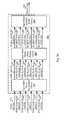
- Sync mark detector circuit 200includes an equalizer circuit 213 that receives a data input 210 and provides an equalized output 215 .
- equalizer circuit 213is a digital finite impulse response filter as are known in the art.
- Data input 210may be a series of digital samples. The digital samples may represent, for example, data stored on a storage medium or data received via a wireless communication medium. Based upon the disclosure provided herein, one of ordinary skill in the art will recognize a variety of sources of data input 210 .
- Equalizer output 215is provided to a sync mark pattern match calculation circuit 220 .
- Sync mark pattern match calculation circuit 220compares equalizer output 215 with a preamble pattern 272 from a hardwired preamble pattern 270 and to a sync mark pattern 293 from a sync mark pattern register 280 .
- Sync mark pattern register 280may either be hard coded, or reprogrammable depending upon the particular implementation.
- the sync mark stored in sync mark pattern register 280is a defined pattern of twenty bits in length.
- hardwired preamble pattern 270includes a repeating portion of a preamble pattern.
- the preamble that precedes the sync mark patternrepeats every two cycles.
- the preamble patternincludes twenty or more bits of the preamble repeating as follows: ‘11001100110011001100’. In such a case, preamble pattern 272 is ‘1100’.
- sync mark pattern match calculation circuit 220yields a number of values corresponding to a difference between equalizer output 215 and various components of preamble pattern 272 and sync mark pattern 293 .
- the comparisonis a Euclidean distance between equalizer output 215 and the particular pattern to which it is being compared in accordance with the following equation:
- sync mark pattern match calculation circuit 220provides a sync match output 231 that corresponds to a comparison between the bits of sync mark pattern 293 and the same number of bits of equalizer output 215 .
- Sync mark pattern match calculation circuit 220also provides: a sync plus N match output 232 that corresponds to a comparison between the bits of sync mark pattern 293 less the most recent N bits of sync mark pattern 293 , and the same number of bits of equalizer output 215 ; a sync plus 2N match output 233 that corresponds to a comparison between the bits of sync mark pattern 293 less the most recent 2N bits of sync mark pattern 293 , and the same number of bits of equalizer output 215 ; a sync plus 3N match output 234 that corresponds to a comparison between the bits of sync mark pattern 293 less the most recent 3N bits of sync mark pattern 293 , and the same number of bits of equalizer output 215 ; a sync plus 4N match output 235 that corresponds to a comparison between the bits of sync mark pattern 293 less the most recent 4N bits of sync mark pattern 293 , and the same number of bits of equalizer output 215 ; a sync plus 5N match output 236 that
- sync mark pattern 293is twenty bits in length, and the value of N is four bits. Based upon the disclosure provided herein, one of ordinary skill in the art will recognize a variety of lengths of sync bit patterns and corresponding values of N that may be used in relation to different embodiments of the present invention.
- FIG. 2 bgraphically shows comparisons yielding the various outputs of a sync mark pattern match calculation circuit 220 that were described above.
- a time line 290shows N-bit preamble pattern 272 repeated a number of times (i.e., elements 281 a , 281 b , 281 c , 281 d , 281 e ) and a number of different N-bit portions (i.e., elements 282 , 283 , 284 , 285 , 286 ) of sync mark pattern 293 lined up in time as they would be expected to be received as part of an incoming data stream.
- sync match output 231corresponds to a comparison (e.g., a Euclidean difference) between equalizer output 215 and the five consecutive N-bit portions 282 , 283 , 284 , 285 , 286 of sync mark pattern 293 .
- Sync plus N match output 232corresponds to a comparison (e.g., a Euclidean difference) between equalizer output 215 and one N-bit portion of the preamble 281 e appended with the four least recent N-bit portions 282 , 283 , 284 , 285 of sync mark pattern 293 .
- Sync plus 2N match output 233corresponds to a comparison (e.g., a Euclidean difference) between equalizer output 215 and two N-bit portions of the preamble 281 d , 281 e appended with the three least recent N-bit portions 282 , 283 , 284 of sync mark pattern 293 .
- Sync plus 3N match output 234corresponds to a comparison (e.g., a Euclidean difference) between equalizer output 215 and three N-bit portions of the preamble 281 c , 281 d , 281 e appended with the two least recent N-bit portions 282 , 283 of sync mark pattern 293 .
- Sync plus 4N match output 235corresponds to a comparison (e.g., a Euclidean difference) between equalizer output 215 and four N-bit portions of the preamble 281 b , 281 c , 281 d , 281 e appended with the least recent N-bit portion 282 of sync mark pattern 293 .
- Sync plus 5N match output 236corresponds to a comparison (e.g., a Euclidean difference) between equalizer output 215 and five N-bit portions of the preamble 281 a , 281 b , 281 c , 281 d , 281 e.
- sync match output 231 , sync plus N match output 232 , sync plus 2N match output 233 , sync plus 3N match output 234 , sync plus 4N match output 235 and sync plus 5N match output 236are provided to a match metric calculation circuit 291 .
- Match metric calculation circuit 291calculates a ratio between each of sync match output 231 , sync plus N match output 232 , sync plus 2N match output 233 , sync plus 3N match output 234 , sync plus 4N match output 235 and sync plus 5N match output 236 and the other match outputs, and selects a minimum value as a match value 295 .
- match metric calculation circuit 291includes a sync mark ratio calculation circuit 201 , a sync mark metric ratio priority circuit 202 , and a sync mark location buffer circuit 203 .
- Sync match output 231 , sync plus N match output 232 , sync plus 2N match output 233 , sync plus 3N match output 234 , sync plus 4N match output 235 and sync plus 5N match output 236are provided from sync mark pattern match calculation circuit 220 to sync mark ratio calculation circuit 201 .
- Sync mark ratio calculation circuit 201calculates a ratio of the minimum of other sync match values and the tested sync match value. In particular, sync mark ratio calculation circuit 201 calculates a ratio for each of Sync match output 231 , sync plus N match output 232 , sync plus 2N match output 233 , sync plus 3N match output 234 , sync plus 4N match output 235 and sync plus 5N match output 236 in accordance with the following equations:
- sync mark metric ratio priority circuit 202places the received ratio values in a priority order with the highest value being identified as a first best sync location 261 (i.e., the location in a data set where the sync mark associated with the highest value sync match ratio value from sync mark ratio calculation circuit 201 ), and the lower values being placed in descending order.
- the prioritized locationsare provided from sync mark metric ratio priority circuit 202 as: first best sync location 261 , a second best sync location 262 , a third best sync location 263 , a fourth best sync location 264 , a fifth best sync location 265 , and a sixth best sync location 266 .
- These priority locationsare stored to a sync mark location buffer circuit 203 .
- Sync mark location buffer circuit 203provides first best sync location 261 as a match value 295 , while maintaining the other lower priority locations for possible future use where the framing of the data set corresponding to first best sync location 261 fails to yield a converged data set.
- match value 295is provided to a sync mark found indication circuit 250 .
- Sync mark found indication circuit 250asserts a sync found output 260 that is located in accordance with match value 295 and used to frame the data set from which the sync mark was found for data processing.
- This framing processmay be any process known in the art that is used to indicate the location of user data within an overall data set including both the user data and the sync mark pattern to which the match value corresponds.
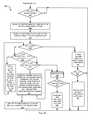
- FIGS. 3 a - 3 bare flow diagrams 300 , 399 showing a method in accordance with one or more embodiments of the present invention for performing a ratio metric based sync mark detection.
- data samplesare received as a data input (block 305 ).
- the received data samplesmay be derived from, for example, a storage medium or a wireless transfer medium. Based upon the disclosure provided herein, one of ordinary skill in the art will recognize a variety of sources of the data samples. It is determined whether Y samples have been received (block 310 ). In some embodiments of the present invention, Y is four bits.
- the most recently received Y bitsare compared with various patterns.
- the most recently received Y bitsare compared with a first sync mark pattern to yield a first comparison (i.e., the Y least significant bits of the sync mark pattern) (block 321 ).
- the comparisonis a Euclidean distance between the received four bits and the first sync mark pattern in accordance with the following equation:
- the most recently received Y bitsare compared with a second sync mark pattern to yield a second comparison (i.e., the next Y least significant bits of the sync mark pattern) (block 323 ).
- the comparisonis a Euclidean distance between the received four bits and the second sync mark pattern in accordance with the following equation:
- the most recently received Y bitsare compared with a third sync mark pattern to yield a third comparison (i.e., the next Y least significant bits of the sync mark pattern) (block 325 ).
- the comparisonis a Euclidean distance between the received four bits and the third sync mark pattern in accordance with the following equation:
- the most recently received Y bitsare compared with a fourth sync mark pattern to yield a fourth comparison (i.e., the next Y least significant bits of the sync mark pattern) (block 327 ).
- the comparisonis a Euclidean distance between the received four bits and the fourth sync mark pattern in accordance with the following equation:
- the most recently received Y bitsare compared with a fifth sync mark pattern to yield a fifth comparison (i.e., the next Y least significant bits of the sync mark pattern) (block 329 ).
- the comparisonis a Euclidean distance between the received four bits and the fifth sync mark pattern in accordance with the following equation:
- the aforementioned comparison outputsare then combined to yield interim outputs.
- the first comparisonis summed with the second comparison delayed by Y bit periods, the third comparison delayed by 2Y bit periods, the fourth comparison delayed by 3Y bit periods, and the fifth comparison delayed by 4Y bit periods to yield a first interim output (block 341 ).
- This first interim outputis provided as a sync match output (block 351 ).
- the second comparisonis summed with the third comparison delayed by Y bit periods, the fourth comparison delayed by 2Y bit periods, the fifth comparison delayed by 3Y bit periods, and the sixth comparison delayed by 4Y bit periods to yield a second interim output (block 343 ).
- This first interim outputis provided as a sync plus N match output (block 353 ).
- the third comparisonis summed with the fourth comparison delayed by Y bit periods, the fifth comparison delayed by 2Y bit periods, the sixth comparison delayed by 3Y bit periods, and the sixth comparison delayed by 4Y bit periods to yield a second interim output (block 345 ).
- This first interim outputis provided as a sync plus 2N match output (block 355 ).
- the fourth comparisonis summed with the fifth comparison delayed by Y bit periods, the sixth comparison delayed by 2Y bit periods, the sixth comparison delayed by 3Y bit periods, and the sixth comparison delayed by 4Y bit periods to yield a second interim output (block 347 ).
- This first interim outputis provided as a sync plus 3N match output (block 357 ).
- the fifth comparisonis summed with the sixth comparison delayed by Y bit periods, the sixth comparison delayed by 2Y bit periods, the sixth comparison delayed by 3Y bit periods, and the sixth comparison delayed by 4Y bit periods to yield a second interim output (block 349 ).
- This first interim outputis provided as a sync plus 4N match output (block 359 ).
- the sixth comparisonis summed with the sixth comparison delayed by Y bit periods, the sixth comparison delayed by 2Y bit periods, the sixth comparison delayed by 3Y bit periods, and the sixth comparison delayed by 4Y bit periods to yield a second interim output (block 333 ).
- This first interim outputis provided as a sync plus 5N match output (block 335 ).
- each of the aforementioned sync match output, the sync plus N match output, the sync plus 2N match output, the sync plus 3N match output, the sync plus 4N match output, and the sync plus 5N match outputare used to calculate sync match ratios for each of the received sync matches (block 380 ).
- a ratio of the minimum of other sync match values and the tested sync match valueis calculated.
- These ratiosmay be calculated for each of the sync match output, the sync plus N match output, the sync plus 2N match output, the sync plus 3N match output, the sync plus 4N match output, and the sync plus 5N match output in accordance with the following equations:
- SYNC ⁇ ⁇ MATCH ⁇ ⁇ R⁇ Min ( SYNC ⁇ ⁇ PLUS ⁇ ⁇ N ⁇ ⁇ MATCH , ⁇ SYNC ⁇ ⁇ PLUS ⁇ ⁇ 2 ⁇ N ⁇ ⁇ MATCH , ⁇ SYNC ⁇ ⁇ PLUS ⁇ ⁇ 3 ⁇ N ⁇ ⁇ MATCH , ⁇ SYNC ⁇ ⁇ PLUS ⁇ ⁇ 4 ⁇ N ⁇ ⁇ MATCH , ⁇ SYNC ⁇ ⁇ PLUS ⁇ ⁇ 5 ⁇ N ⁇ ⁇ MATCH ) / ⁇ SYNC ⁇ ⁇ MATCH ;
- SYNC ⁇ ⁇ MATCH ⁇ ⁇ N ⁇ ⁇ R⁇ Min ( SYNC ⁇ ⁇ MATCH , ⁇ SYNC ⁇ ⁇ PLUS ⁇ ⁇ 2 ⁇ N ⁇ ⁇ MATCH , ⁇ SYNC ⁇ ⁇ PLUS ⁇ ⁇ 3 ⁇ N ⁇ ⁇ MATCH , ⁇ SYNC ⁇
- sync match ratio values(Sync Match R, Sync Match N R, Sync Match 2N R, Sync Match 3N R, Sync Match 4N R, Sync Match 5N R) are used to determine an occurrence of a sync mark (block 385 ). It is determined whether one of the sync match ratio values is substantially greater than unity (block 390 ). In one particular embodiment of the present invention, it is determined whether one of the sync match ratio values is greater than 1.4. Based upon the disclosure provided herein, one of ordinary skill in the art will recognize a variety of threshold values that may be used in relation to different embodiments of the present invention to determine whether a sync mark has been found. Where it is determined that the sync mark was found (block 390 ), a sync mark found output is asserted (block 395 ).
- Data processing circuit 400includes an analog front end circuit 410 that receives an analog input 408 .
- Analog front end circuit 410processes analog input 408 and provides a processed analog signal 412 to an analog to digital converter circuit 415 .
- Analog front end circuit 410may include, but is not limited to, an analog filter and an amplifier circuit as are known in the art. Based upon the disclosure provided herein, one of ordinary skill in the art will recognize a variety of circuitry that may be included as part of analog front end circuit 410 .
- analog input 408is derived from a read/write head assembly (not shown) that is disposed in relation to a storage medium (not shown). In other cases, analog input 408 is derived from a receiver circuit (not shown) that is operable to receive a signal from a transmission medium (not shown).
- the transmission mediummay be wired or wireless.
- Analog to digital converter circuit 415converts processed analog signal 412 into a corresponding series of digital samples 417 .
- Analog to digital converter circuit 415may be any circuit known in the art that is capable of producing digital samples corresponding to an analog input signal. Based upon the disclosure provided herein, one of ordinary skill in the art will recognize a variety of analog to digital converter circuits that may be used in relation to different embodiments of the present invention.
- Digital samples 417are provided to an equalizer circuit 420 .
- Equalizer circuit 420applies an equalization algorithm to digital samples 417 to yield an equalized output 422 .
- equalizer circuit 420is a digital finite impulse response filter circuit as are known in the art.
- Equalized output 422is provided to a data detector circuit 425 , a sample buffer circuit 475 , and a sync mark detection and framing circuit 490 .
- Sync mark detection and framing circuit 490includes a ratio metric based sync mark detector circuit similar to that discussed above in relation to FIGS. 2 a - 2 c .
- Sync mark detection and framing circuit 490applies the aforementioned ratio based sync mark detection algorithm to identify one or more possible sync marks.
- the sync marksare used to generate a framing signal 493 that is used to indicate a location of the beginning of a user data set within equalized output 422 .
- Sample buffer circuit 475stores equalized output 422 as buffered data 477 for use in subsequent iterations through data detector circuit 425 .
- Data detector circuit 425may be any data detector circuit known in the art that is capable of producing a detected output 427 .
- data detector circuit 425may be, but is not limited to, a Viterbi algorithm detector circuit or a maximum a posteriori detector circuit as are known in the art.
- the general phrases “Viterbi data detection algorithm” or “Viterbi algorithm data detector circuit”are used in their broadest sense to mean any Viterbi detection algorithm or Viterbi algorithm detector circuit or variations thereof including, but not limited to, bi-direction Viterbi detection algorithm or bi-direction Viterbi algorithm detector circuit.
- maximum a posteriori data detection algorithmor “maximum a posteriori data detector circuit” are used in their broadest sense to mean any maximum a posteriori detection algorithm or detector circuit or variations thereof including, but not limited to, simplified maximum a posteriori data detection algorithm and a max-log maximum a posteriori data detection algorithm, or corresponding detector circuits. Based upon the disclosure provided herein, one of ordinary skill in the art will recognize a variety of data detector circuits that may be used in relation to different embodiments of the present invention.
- Detected output 425may include both hard decisions and soft decisions. The terms “hard decisions” and “soft decisions” are used in their broadest sense.
- hard decisionsare outputs indicating an expected original input value (e.g., a binary ‘1’ or ‘0’, or a non-binary digital value), and the “soft decisions” indicate a likelihood that corresponding hard decisions are correct.
- an expected original input valuee.g., a binary ‘1’ or ‘0’, or a non-binary digital value
- Detected output 427is provided to a central queue memory circuit 460 that operates to buffer data passed between data detector circuit 425 and data decoder circuit 450 .
- central queue memory circuit 460includes interleaving (i.e., data shuffling) and de-interleaving (i.e., data un-shuffling) circuitry known in the art.
- data decoder circuit 450accesses detected output 427 from central queue memory circuit 460 as a decoder input 456 .
- Data decoder circuit 450applies a data decoding algorithm to decoder input 456 in an attempt to recover originally written data. The result of the data decoding algorithm is provided as a decoded output 452 .
- decoded output 452may include both hard decisions and soft decisions.
- data decoder circuit 450may be any data decoder circuit known in the art that is capable of applying a decoding algorithm to a received input.
- Data decoder circuit 450may be, but is not limited to, a low density parity check (LDPC) decoder circuit or a Reed Solomon decoder circuit as are known in the art. Based upon the disclosure provided herein, one of ordinary skill in the art will recognize a variety of data decoder circuits that may be used in relation to different embodiments of the present invention.
- LDPClow density parity check
- decoded output 452is stored to a memory included in a hard decision output circuit 480 .
- hard decision output circuit 480provides the converged decoded output 452 as a data output 484 to a recipient (not shown).
- the recipientmay be, for example, an interface circuit operable to receive processed data sets. Based upon the disclosure provided herein, one of ordinary skill in the art will recognize a variety of recipients that may be used in relation to different embodiments of the present invention.
- decoded output 452indicates that the data is unusable as is more specifically discussed below, and data output 484 is similarly identified as unusable.
- Data decoder circuit 453additionally provides a framing signal selection signal 453 to sync mark detection and framing circuit 490 that causes sync mark detection and framing circuit 490 to provide a next best framing signal 493 .
- Equalized output 422is then re-processed using the new framing signal 493 indicating a different starting location of user data in equalized output 422 .
- framing signal selection signal 453is asserted to cause another framing signal to be provided under particular conditions.
- Such conditionsmay include, for example, a failure of data decoder circuit 450 to converge after a defined number of global iterations, and/or where a number of unsatisfied checks exceed a defined level after a defined number of global iterations have occurred in relation to the currently processing data set.
- a failure of data decoder circuit 450 to converge after a defined number of global iterationsand/or where a number of unsatisfied checks exceed a defined level after a defined number of global iterations have occurred in relation to the currently processing data set.
- One or more iterations through the combination of data detector circuit 425 and data decoder circuit 450may be made in an effort to converge on the originally written data set.
- processing through both the data detector circuit and the data decoder circuitis referred to as a “global iteration”.
- data detector circuit 425applies the data detection algorithm to equalized output 422 without guidance from a decoded output.
- data detector circuit 425applies the data detection algorithm to buffered data 477 as guided by decoded output 452 .
- decoded output 452is stored to central queue memory circuit 460 as a decoder output 454 , and is provided from central queue memory circuit 460 as a detector input 429 when equalized output 422 is being re-processed through data detector circuit 425 .
- data decoder circuit 450During each global iteration it is possible for data decoder circuit 450 to make one or more local iterations including application of the data decoding algorithm to decoder input 456 .
- data decoder circuit 450applies the data decoder algorithm without guidance from decoded output 452 .
- data decoder circuit 450applies the data decoding algorithm to decoder input 456 as guided by a previous decoded output 452 .
- the number of local iterations allowedmay be, for example, ten. Based upon the disclosure provided herein, one of ordinary skill in the art will recognize a variety of different numbers of local iterations that may be allowed in accordance with different embodiments of the present invention.
- decoded output 452is provided back to central queue memory circuit 460 as decoded output 454 .
- Decoded output 454is maintained in central queue memory circuit 460 until data detector circuit 425 becomes available to perform additional processing.
- flow diagrams 500 , 545show a method in accordance with one or more embodiments of the present invention for data processing using different sync marks prioritized based upon a ratio metric.
- an analog inputis received (block 505 ).
- the analog inputmay be derived from, for example, a storage medium or a data transmission channel. Based upon the disclosure provided herein, one of ordinary skill in the art will recognize a variety of sources of the analog input.
- the analog inputis converted to a series of digital samples (block 510 ). This conversion may be done using an analog to digital converter circuit or system as are known in the art.
- any circuit known in the art that is capable of converting an analog signal into a series of digital values representing the received analog signalmay be used.
- the resulting digital samplesare equalized to yield an equalized output (block 515 ).
- the equalizationis done using a digital finite impulse response circuit as are known in the art. Based upon the disclosure provided herein, one of ordinary skill in the art will recognize a variety of equalizer circuits that may be used in place of such a digital finite impulse response circuit to perform equalization in accordance with different embodiments of the present invention.
- the equalized outputis buffered (block 520 ).
- a main data detector circuitIt is determined whether a main data detector circuit is available (block 525 ). Where the main data detector circuit is available (block 525 ), the next equalized output from the sample buffer is selected for processing (block 530 ), and a data detection is performed on the selected equalized output to yield a detected output (block 535 ). The detected output is then stored to a central memory (block 540 ).
- a decoder circuitis available to process a previously stored the detected output (block 501 ). Where the decoder circuit is available (block 501 ), the next derivative of a detected output is selected for processing and accessed from the central memory circuit (block 506 ). A first local iteration of a data decoding algorithm is applied by the data decoder circuit to the selected detected output to yield a decoded output (block 511 ).
- the data decoding algorithmis a low density parity check algorithm.
- the decoded outputconverged (i.e., yielded a correct result) (block 516 ).
- the decoded outputis provided to a hard decision output buffer (block 521 ).
- the hard decision output bufferis ready to be unloaded (block 556 ). In some cases, the hard decision output buffer is ready to be unloaded when the most recently completed decoded output is the next decoded output after that previously provided as a data output.
- the hard decision output bufferis ready to be unloaded (block 556 )
- all of the continuous decoded outputs maintained in the hard decision output bufferare provided as a data output to a recipient device (block 561 ). Based upon the disclosure provided herein, one of ordinary skill in the art will recognize a variety of recipient devices that may be used in relation to different embodiments of the present invention.
- the decoded outputfailed to converge (block 516 )
- This local iteration limitmay be, for example, ten local iterations.
- the data decoding algorithmis re-applied to the currently processing data set for a subsequent local iteration guided by the decoded output to yield an updated decoded output (block 531 ). The processes beginning at block 516 are then repeated.
- the number of local iterations for the currently proceeding global iterationhave been exceeded (block 526 )
- the number of global iterationsmay be complete where, for example, a timeout condition has occurred or a memory usage limitation has been exceeded.
- the decoded outputis stored to the central memory where it awaits use in guiding application of the data detection algorithm during a subsequent global iteration (block 541 ).
- an erroris indicated (block 546 ) and it is determined whether another framing of the received data set is possible (block 581 ). Another framing is possible where another possible sync mark was detected in addition to the sync mark that was used for the original framing and the currently proceeding data processing. Where another framing is possible (block 581 ), the next framing is selected (block 586 ) and processing (i.e., the processes of FIGS. 5 a - 5 b ) is restarted using the next best sync mark to apply framing.
- Communication system 600includes a transmitter 610 that is operable to transmit encoded information via a transfer medium 630 as is known in the art.
- the encoded datais received from transfer medium 630 by receiver 620 .
- the ratio metric based sync mark detector circuit included in receiver 620may be similar to that discussed above in relation to FIGS. 2 a - 2 c , and/or may operate in accordance with the method discussed above in relation to FIGS. 3 a - 3 b .
- the ratio metric based sync mark detector circuitis incorporated in a data processing circuit that itself is included in receiver 620 .
- the data processing circuitmay operate in accordance with the method discussed above in relation to FIGS. 5 a - 5 b.
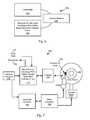
- Storage system 700including a read channel circuit 710 with a ratio metric based sync mark detector circuit is shown in accordance with various embodiments of the present invention.
- Storage system 700may be, for example, a hard disk drive.
- Storage system 700also includes a preamplifier 770 , an interface controller 720 , a hard disk controller 766 , a motor controller 768 , a spindle motor 772 , a disk platter 778 , and a read/write head 776 .
- Interface controller 720controls addressing and timing of data to/from disk platter 778 .
- the data on disk platter 778consists of groups of magnetic signals that may be detected by read/write head assembly 776 when the assembly is properly positioned over disk platter 778 .
- disk platter 778includes magnetic signals recorded in accordance with either a longitudinal or a perpendicular recording scheme.
- read/write head assembly 776is accurately positioned by motor controller 768 over a desired data track on disk platter 778 .
- Motor controller 768both positions read/write head assembly 776 in relation to disk platter 778 and drives spindle motor 772 by moving read/write head assembly to the proper data track on disk platter 778 under the direction of hard disk controller 766 .
- Spindle motor 772spins disk platter 778 at a determined spin rate (RPMs).
- the sensed magnetic signalsare provided as a continuous, minute analog signal representative of the magnetic data on disk platter 778 .
- This minute analog signalis transferred from read/write head assembly 776 to read channel module 764 via preamplifier 770 .
- Preamplifier 770is operable to amplify the minute analog signals accessed from disk platter 778 .
- read channel circuit 710decodes and digitizes the received analog signal to recreate the information originally written to disk platter 778 .
- This datais provided as read data 703 to a receiving circuit. As part of decoding the received information, read channel circuit 710 performs a sync mark detection process.
- Such a sync mark detection processmay be performed using a ratio metric based sync mark detector circuit included in read channel circuit 710 may be similar to that discussed above in relation to FIGS. 2 a - 2 c , and/or may operate in accordance with the method discussed above in relation to FIGS. 3 a - 3 b .
- the ratio metric based sync mark detector circuitis incorporated in a data processing circuit that itself is included in read channel circuit 710 . In such cases, the data processing circuit may operate in accordance with the method discussed above in relation to FIGS. 5 a - 5 b.
- storage system 700may be integrated into a larger storage system such as, for example, a RAID (redundant array of inexpensive disks or redundant array of independent disks) based storage system.
- RAIDredundant array of inexpensive disks or redundant array of independent disks
- Such a RAID storage systemincreases stability and reliability through redundancy, combining multiple disks as a logical unit.
- Datamay be spread across a number of disks included in the RAID storage system according to a variety of algorithms and accessed by an operating system as if it were a single disk. For example, data may be mirrored to multiple disks in the RAID storage system, or may be sliced and distributed across multiple disks in a number of techniques.
- the disks in the RAID storage systemmay be, but are not limited to, individual storage systems such as storage system 700 , and may be located in close proximity to each other or distributed more widely for increased security.
- write datais provided to a controller, which stores the write data across the disks, for example by mirroring or by striping the write data.
- the controllerretrieves the data from the disks. The controller then yields the resulting read data as if the RAID storage system were a single disk.
- a data decoder circuit used in relation to read channel circuit 710may be, but is not limited to, a low density parity check (LDPC) decoder circuit as are known in the art.
- LDPClow density parity check
- Transmission applicationsinclude, but are not limited to, optical fiber, radio frequency channels, wired or wireless local area networks, digital subscriber line technologies, wireless cellular, Ethernet over any medium such as copper or optical fiber, cable channels such as cable television, and Earth-satellite communications.
- Storage applicationsinclude, but are not limited to, hard disk drives, compact disks, digital video disks, magnetic tapes and memory devices such as DRAM, NAND flash, NOR flash, other non-volatile memories and solid state drives.
- Such integrated circuitsmay include all of the functions of a given block, system or circuit, or only a subset of the block, system or circuit. Further, elements of the blocks, systems or circuits may be implemented across multiple integrated circuits. Such integrated circuits may be any type of integrated circuit known in the art including, but are not limited to, a monolithic integrated circuit, a flip chip integrated circuit, a multichip module integrated circuit, and/or a mixed signal integrated circuit. It should also be noted that various functions of the blocks, systems or circuits discussed herein may be implemented in either software or firmware. In some such cases, the entire system, block or circuit may be implemented using its software or firmware equivalent. In other cases, the one part of a given system, block or circuit may be implemented in software or firmware, while other parts are implemented in hardware.
Landscapes
- Engineering & Computer Science (AREA)
- Signal Processing (AREA)
- Signal Processing For Digital Recording And Reproducing (AREA)
Abstract
Description
where k represents an individual sample value. In particular, sync mark pattern
In addition, the most recently received Y bits are compared with a second sync mark pattern to yield a second comparison (i.e., the next Y least significant bits of the sync mark pattern) (block323). In some cases, the comparison is a Euclidean distance between the received four bits and the second sync mark pattern in accordance with the following equation:
In addition, the most recently received Y bits are compared with a third sync mark pattern to yield a third comparison (i.e., the next Y least significant bits of the sync mark pattern) (block325). In some cases, the comparison is a Euclidean distance between the received four bits and the third sync mark pattern in accordance with the following equation:
In addition, the most recently received Y bits are compared with a fourth sync mark pattern to yield a fourth comparison (i.e., the next Y least significant bits of the sync mark pattern) (block327). In some cases, the comparison is a Euclidean distance between the received four bits and the fourth sync mark pattern in accordance with the following equation:
In addition, the most recently received Y bits are compared with a fifth sync mark pattern to yield a fifth comparison (i.e., the next Y least significant bits of the sync mark pattern) (block329). In some cases, the comparison is a Euclidean distance between the received four bits and the fifth sync mark pattern in accordance with the following equation:
In addition, the most recently received Y bits are compared with a Y bit preamble pattern to yield a sixth comparison (i.e., the next Y least significant bits of the sync mark pattern) (block331). In some cases, the comparison is a Euclidean distance between the received four bits and the fifth sync mark pattern in accordance with the following equation:
Claims (20)
Priority Applications (1)
| Application Number | Priority Date | Filing Date | Title |
|---|---|---|---|
| US13/529,572US8564897B1 (en) | 2012-06-21 | 2012-06-21 | Systems and methods for enhanced sync mark detection |
Applications Claiming Priority (1)
| Application Number | Priority Date | Filing Date | Title |
|---|---|---|---|
| US13/529,572US8564897B1 (en) | 2012-06-21 | 2012-06-21 | Systems and methods for enhanced sync mark detection |
Publications (1)
| Publication Number | Publication Date |
|---|---|
| US8564897B1true US8564897B1 (en) | 2013-10-22 |
Family
ID=49355261
Family Applications (1)
| Application Number | Title | Priority Date | Filing Date |
|---|---|---|---|
| US13/529,572ActiveUS8564897B1 (en) | 2012-06-21 | 2012-06-21 | Systems and methods for enhanced sync mark detection |
Country Status (1)
| Country | Link |
|---|---|
| US (1) | US8564897B1 (en) |
Cited By (4)
| Publication number | Priority date | Publication date | Assignee | Title |
|---|---|---|---|---|
| US8687301B1 (en)* | 2013-01-08 | 2014-04-01 | Lsi Corporation | Parallel no-sync-mark retry |
| US8760977B2 (en)* | 2011-04-28 | 2014-06-24 | Lsi Corporation | Systems and methods for data write loopback based timing control |
| US8837263B1 (en)* | 2013-03-22 | 2014-09-16 | Lsi Corporation | Automatic on-drive sync-mark search and threshold adjustment |
| US8976475B1 (en) | 2013-11-12 | 2015-03-10 | Lsi Corporation | Systems and methods for large sector dynamic format insertion |
Citations (160)
| Publication number | Priority date | Publication date | Assignee | Title |
|---|---|---|---|---|
| US4777544A (en) | 1986-08-15 | 1988-10-11 | International Business Machine Corporation | Method and apparatus for in-situ measurement of head/recording medium clearance |
| US5130866A (en) | 1990-07-17 | 1992-07-14 | International Business Machines Corporation | Method and circuitry for in-situ measurement of transducer/recording medium clearance and transducer magnetic instability |
| US5237325A (en) | 1989-11-21 | 1993-08-17 | Klein Hans Christoph | Process and system for gathering and evaluating measured data |
| US5278703A (en) | 1991-06-21 | 1994-01-11 | Digital Equipment Corp. | Embedded servo banded format for magnetic disks for use with a data processing system |
| US5309357A (en) | 1992-01-28 | 1994-05-03 | Independent Scintillation Imaging Systems (Isis) Inc. | Scintillation data collecting apparatus and method |
| US5341249A (en) | 1992-08-27 | 1994-08-23 | Quantum Corporation | Disk drive using PRML class IV sampling data detection with digital adaptive equalization |
| US5377058A (en) | 1992-12-31 | 1994-12-27 | International Business Machines Corporation | Fly height servo control of read/write head suspension |
| US5521948A (en) | 1994-04-28 | 1996-05-28 | Sony Corporation | Frequency synthesizer |
| US5523902A (en) | 1993-10-25 | 1996-06-04 | Syquest Technology, Inc. | Servo burst pattern for removing offset caused by magnetic distortion and method associated therewith |
| US5594341A (en) | 1994-06-27 | 1997-01-14 | Varian Associates, Inc. | Nuclear magnetic resonance receiver, method and system |
| US5668679A (en) | 1995-12-21 | 1997-09-16 | Quantum Corporation | System for self-servowriting a disk drive |
| US5696639A (en) | 1995-05-12 | 1997-12-09 | Cirrus Logic, Inc. | Sampled amplitude read channel employing interpolated timing recovery |
| US5768044A (en) | 1993-12-23 | 1998-06-16 | International Business Machines Corporation | Zoned recording embedded servo disk drive having no data identification fields and reduced rotational latency |
| US5781129A (en) | 1997-03-03 | 1998-07-14 | Motorola, Inc. | Adaptive encoder circuit for multiple data channels and method of encoding |
| US5798885A (en) | 1994-06-06 | 1998-08-25 | Fujitsu Limited | Head positioning control for disk apparatus using peak detection, polarity detection and sector mark detection |
| US5835295A (en) | 1996-11-18 | 1998-11-10 | Cirrus Logice, Inc. | Zero phase restart interpolated timing recovery in a sampled amplitude read channel |
| US5844920A (en) | 1996-11-07 | 1998-12-01 | Cirrus Logic, Inc. | Thermal asperity compensation using multiple sync marks for retroactive and split segment data synchronization in a magnetic disk storage system |
| US5852524A (en) | 1997-02-07 | 1998-12-22 | Cirrus Logic, Inc. | Sampled amplitude read channel for processing multiple data streams in a disc storage system |
| US5892632A (en) | 1996-11-18 | 1999-04-06 | Cirrus Logic, Inc. | Sampled amplitude read channel employing a residue number system FIR filter in an adaptive equalizer and in interpolated timing recovery |
| US5955783A (en) | 1997-06-18 | 1999-09-21 | Lsi Logic Corporation | High frequency signal processing chip having signal pins distributed to minimize signal interference |
| US5970104A (en) | 1997-03-19 | 1999-10-19 | Cadence Design Systems, Inc. | Method and apparatus for generating branch metrics and branch indices for convolutional code Viterbi decoders |
| US5987562A (en) | 1996-03-08 | 1999-11-16 | Texas Instruments Incorporated | Waveform sampler and method for sampling a signal from a read channel |
| US5986830A (en) | 1997-07-30 | 1999-11-16 | Cirrus Logic, Inc. | Read/write channel write precompensation system and method using one or more delay clocks |
| US6009549A (en) | 1997-05-15 | 1999-12-28 | Cirrus Logic, Inc. | Disk storage system employing error detection and correction of channel coded data, interpolated timing recovery, and retroactive/split-segment symbol synchronization |
| US6023383A (en) | 1996-03-19 | 2000-02-08 | Texas Instruments Incorporated | Error estimation circuit and method for providing a read channel error signal |
| US6069583A (en) | 1996-05-09 | 2000-05-30 | Agence Spatiale Europeene | Receiver for a navigation system, in particular a satellite navigation system |
| US6081397A (en) | 1997-04-08 | 2000-06-27 | International Business Machines Corporation | Method and apparatus for SID-to-SID period estimation |
| US6111712A (en) | 1998-03-06 | 2000-08-29 | Cirrus Logic, Inc. | Method to improve the jitter of high frequency phase locked loops used in read channels |
| US6208478B1 (en) | 1998-07-07 | 2001-03-27 | Texas Instruments Incorporated | Read clock interface for read channel device |
| US6269058B1 (en) | 1999-01-04 | 2001-07-31 | Texas Instruments Incorporated | Wide capture range circuitry |
| US6278591B1 (en) | 1998-04-02 | 2001-08-21 | International Business Machines Corporation | Inverted merged MR head having plated notched first pole tip and self-aligned second pole tip |
| US6400518B1 (en) | 2000-11-01 | 2002-06-04 | International Business Machines Corporation | Magneto-resistive asymmetry correction circuit |
| US6404829B1 (en) | 1999-06-29 | 2002-06-11 | Oak Technology, Inc. | DC insensitive AGC circuit for optical PRML read channel |
| US6411452B1 (en) | 1997-03-11 | 2002-06-25 | Western Digital Technologies, Inc. | Disk drive employing read error tolerant sync mark detection |
| US6441661B1 (en) | 1998-06-30 | 2002-08-27 | Asahi Kasei Kabushiki Kaisha | PLL circuit |
| US20020150179A1 (en) | 1994-10-11 | 2002-10-17 | Maxtor Corporation | Synchronous detection of wide bi-phase coded servo information for disk drive |
| US6476989B1 (en) | 1996-07-09 | 2002-11-05 | International Business Machines Corporation | Radial self-propagation pattern generation for disk file servowriting |
| US6490110B2 (en) | 2000-12-05 | 2002-12-03 | Cirrus Logic, Inc. | Servo data detection with improved phase shift tolerance |
| US6493162B1 (en) | 1997-12-05 | 2002-12-10 | Seagate Technology Llc | Frame synchronization for viterbi detector |
| US6519102B1 (en) | 2000-04-27 | 2003-02-11 | International Business Machines Corporation | Method and apparatus for implementing an in-situ digital harmonic computation facility for direct access storage device (DASD) |
| US6530060B1 (en) | 2000-02-08 | 2003-03-04 | Cirrus Logic, Inc. | Sampled amplitude read channel employing a post processor with a boundary error compensator which compensates for boundary error events in a split-field data sector |
| US6603622B1 (en) | 2001-02-28 | 2003-08-05 | Western Digital Technologies, Inc. | Disk drive employing a sync mark detector comprising a matched filter and a dual polarity correlator |
| US6606048B1 (en) | 2000-11-16 | 2003-08-12 | Marvell International, Ltd. | Method and apparatus for equalizing the digital performance of multiple ADC's |
| US6633447B2 (en) | 2001-05-25 | 2003-10-14 | Infineon Technologies Ag | Method and apparatus for compensation of second order distortion |
| US20030193880A1 (en)* | 2000-01-14 | 2003-10-16 | Shigeru Furumiya | Optical disc and optical disc address reading apparatus and method |
| US6646822B1 (en) | 1995-05-12 | 2003-11-11 | Cirrus Logic, Inc. | Sampled amplitude read channel employing pipelined reads to reduce the gap between sectors |
| US6657802B1 (en) | 1999-04-16 | 2003-12-02 | Infineon Technologies Corporation | Phase assisted synchronization detector |
| US6671404B1 (en) | 1997-02-14 | 2003-12-30 | Hewlett-Packard Development Company, L.P. | Method and apparatus for recognizing patterns |
| US6717764B2 (en) | 2000-06-02 | 2004-04-06 | Seagate Technology Llc | Method and apparatus for head fly height measurement |
| US6775529B1 (en) | 2000-07-31 | 2004-08-10 | Marvell International Ltd. | Active resistive summer for a transformer hybrid |
| US6788484B2 (en) | 2000-12-07 | 2004-09-07 | Nec Corporation | PLL circuit, data detection circuit and disk apparatus |
| US6813108B2 (en) | 2001-10-24 | 2004-11-02 | Agere Systems Inc. | Servo data detection in presence of radial incoherence using multiple data detectors |
| US6816328B2 (en) | 2000-06-20 | 2004-11-09 | Infineon Technologies North America Corp. | Pseudo-synchronous interpolated timing recovery for a sampled amplitude read channel |
| US6839014B2 (en) | 2001-06-27 | 2005-01-04 | Renesas Technology Corp. | One-chip microcomputer with analog-to-digital converter |
| US6856183B2 (en) | 2001-10-12 | 2005-02-15 | Agere Systems Inc. | Scheme to improve performance of timing recovery systems for read channels in a disk drive |
| US6865040B2 (en) | 2001-05-22 | 2005-03-08 | Seagate Technology, Llc | Method and system for measuring fly height |
| US6876511B2 (en) | 2002-08-30 | 2005-04-05 | Kabushiki Kaisha Toshiba | Disk drive and method of detecting servo address mark in the same |
| US6906990B2 (en) | 2001-04-27 | 2005-06-14 | Sony Corporation | Phase-change optical disk and optical disk apparatus |
| US6912099B2 (en) | 2003-05-13 | 2005-06-28 | Agere Systems Inc. | Maximum likelihood detection of asynchronous servo data employing interpolation |
| US20050243455A1 (en) | 2004-04-30 | 2005-11-03 | Viswanath Annampedu | Method and apparatus for improved address mark detection |
| US6963521B2 (en) | 2001-03-30 | 2005-11-08 | Sony Corporation | Disc drive apparatus |
| US6980382B2 (en) | 2001-11-09 | 2005-12-27 | Fujitsu Limited | Magnetic disk drive system |
| US6999257B2 (en) | 2001-01-31 | 2006-02-14 | Kabushiki Kaisha Toshiba | Magnetic disk drive with structure for avoiding DC magnetic disturbance on a disk surface |
| US6999264B2 (en) | 2002-12-27 | 2006-02-14 | Matsushita Electric Industrial Co., Ltd. | Methods for variable multi-pass servowriting and self-servowriting |
| US7002767B2 (en) | 2003-09-30 | 2006-02-21 | Agere Systems Inc. | Detection of recorded data employing interpolation with gain compensation |
| US7016131B2 (en) | 2003-08-29 | 2006-03-21 | Agency For Science, Technology And Research | Method and implementation of in-situ absolute head medium spacing measurement |
| US7038875B2 (en) | 2003-07-31 | 2006-05-02 | Seagate Technology Llc | Dynamic measurement of head media spacing modulation |
| US7054088B2 (en) | 2002-01-21 | 2006-05-30 | Fujitsu Limited | Information recording and reproducing apparatus and method, and signal decoding circuit for performing timing recovery |
| US7072137B2 (en) | 2002-06-11 | 2006-07-04 | Fujitsu Limited | Data read device, read method and circuit controlling read device |
| US7082005B2 (en) | 2001-10-24 | 2006-07-25 | Agere Systems Inc. | Servo data detection in the presence or absence of radial incoherence using digital interpolators |
| US7092462B2 (en) | 2003-01-14 | 2006-08-15 | Agere Systems Inc. | Asynchronous servo RRO detection employing interpolation |
| US7116504B1 (en) | 2003-03-25 | 2006-10-03 | Marvell International Ltd. | DC-offset compensation loops for magnetic recording system |
| US7126776B1 (en) | 2002-04-17 | 2006-10-24 | Western Digital Technologies, Inc. | Disk drive having a sector clock that is synchronized to the angular speed of the spindle motor |
| US7133227B2 (en) | 2004-01-21 | 2006-11-07 | Seagate Technology Llc | Head polarity detection algorithm and apparatus |
| US7136250B1 (en) | 2003-03-25 | 2006-11-14 | Marvell International Ltd. | Detecting fly height of a head over a storage medium |
| US7154689B1 (en) | 2004-02-05 | 2006-12-26 | Maxtor Corporation | Apparatus for writing servo bursts on a disk with servo track pitch based on read element width and methods of manufacturing same |
| US7158464B2 (en) | 2000-12-26 | 2007-01-02 | Matsushita Electric Industrial Co., Ltd. | Recording medium, recording method, reproduction method, recording apparatus and reproduction apparatus |
| US7167328B2 (en) | 2004-12-17 | 2007-01-23 | Agere Systems Inc. | Synchronizing an asynchronously detected servo signal to synchronous servo demodulation |
| US7180693B2 (en) | 2004-04-14 | 2007-02-20 | Agere Systems Inc. | Method and apparatus for maximum likelihood detection of data employing interpolation with compensation of signal asymmetry |
| US7187739B2 (en) | 2002-05-20 | 2007-03-06 | Via Technologies, Inc. | Timing recovery circuit |
| US7191382B2 (en) | 2003-06-02 | 2007-03-13 | Fujitsu Limited | Methods and apparatus for correcting data and error detection codes on the fly |
| US7193798B2 (en) | 2005-01-12 | 2007-03-20 | Agere Systems, Inc. | Method and apparatus for encoding and decoding a runout correction bit pattern of servo field |
| US7193544B1 (en) | 2004-09-08 | 2007-03-20 | Northrop Grumman Corporation | Parallel, adaptive delta sigma ADC |
| US7199961B1 (en) | 2003-03-25 | 2007-04-03 | Marvell International Ltd. | Detecting fly height of a head over a storage medium |
| US7203015B2 (en) | 2003-07-31 | 2007-04-10 | Kabushiki Kaisha Toshiba | Method and apparatus for decoding sync marks in a disk |
| US7203013B1 (en) | 2004-07-26 | 2007-04-10 | Marvell International Ltd. | Method and apparatus for asymmetry correction in magnetic recording channels |
| US7206146B2 (en) | 2004-10-27 | 2007-04-17 | Hitachi Global Storage Technologies Netherlands B.V. | Biphase magnetic pattern detector using multiple matched filters for hard disk drive |
| US20070104300A1 (en) | 2005-09-22 | 2007-05-10 | Atsushi Esumi | Signal processing apparatus, signal processing method and storage system |
| US7230789B1 (en) | 2004-04-08 | 2007-06-12 | Maxtor Corporation | Method and apparatus for performing a self-servo write operation in a disk drive using spiral servo information |
| US7248425B2 (en) | 2004-12-14 | 2007-07-24 | Samsung Electronics Co., Ltd. | Disk writing/reproducing apparatus and method |
| US7253984B1 (en) | 2004-09-02 | 2007-08-07 | Maxtor Corporation | Disk drive that generates a position error signal and a fly height signal from a servo burst pattern |
| US7265937B1 (en) | 2006-06-09 | 2007-09-04 | Seagate Technology Llc | Positioning of a head array over a data storage medium |
| US7286313B2 (en) | 2004-05-26 | 2007-10-23 | Seagate Technology, Llc | Correcting radial incoherence in servo track sensing |
| US7301717B1 (en) | 2004-07-30 | 2007-11-27 | Western Digital Technologies, Inc. | Servo writing a disk drive by integrating a spiral track read signal |
| US7308057B1 (en) | 2003-06-05 | 2007-12-11 | Maxtor Corporation | Baseline wander compensation for perpendicular recording |
| FR2904168A1 (en) | 2006-07-18 | 2008-01-25 | Thales Sa | SYSTEM FOR ESTIMATING THE RECEPTION QUALITY OF A DIGITAL TRANSMISSION. |
| US7323916B1 (en) | 2005-12-07 | 2008-01-29 | Netlogic Microsystems, Inc. | Methods and apparatus for generating multiple clocks using feedback interpolation |
| US20080056403A1 (en) | 2006-09-01 | 2008-03-06 | On Demand Microelectronics | Method and apparatus for timing recovery of pam signals |
| US7362536B1 (en) | 2005-07-08 | 2008-04-22 | Maxtor Corporation | Disk drive that compensates for phase incoherence between radially adjacent servo tracks and methods thereof |
| US7375918B1 (en) | 2002-04-23 | 2008-05-20 | Maxtor Corporation | Method of self-servo writing in a disk drive using multiple timing windows |
| US7394608B2 (en) | 2005-08-26 | 2008-07-01 | International Business Machines Corporation | Read channel apparatus for asynchronous sampling and synchronous equalization |
| US7411531B2 (en) | 2006-06-30 | 2008-08-12 | Agere Systems Inc. | Methods and apparatus for asynchronous sampling of a received signal at a downsampled rate |
| US7420498B2 (en) | 2006-11-22 | 2008-09-02 | Infineon Technologies Ag | Signal converter performing a role |
| US7423827B2 (en) | 2006-04-20 | 2008-09-09 | Agere Systems Inc. | Systems and methods for accessing data from a variable polarity head assembly |
| US7446690B2 (en) | 2006-11-06 | 2008-11-04 | Atmel Corporation | Apparatus and method for implementing an analog-to-digital converter in programmable logic devices |
| US7525460B1 (en) | 2006-07-13 | 2009-04-28 | Marvell International Ltd. | Timing loop based on analog to digital converter output and method of use |
| US7529320B2 (en) | 2005-09-16 | 2009-05-05 | Agere Systems Inc. | Format efficient timing acquisition for magnetic recording read channels |
| US20090142620A1 (en) | 2004-06-22 | 2009-06-04 | Kabushiki Kaisha Toshiba | Magnetic recording medium, method of manufacturing the same, and magnetic recording/reproducing apparatus |
| US7558177B2 (en) | 2005-02-04 | 2009-07-07 | Panasonic Corporation | Optical disc playback apparatus |
| US7602568B1 (en) | 2006-02-24 | 2009-10-13 | Marvell International Ltd. | Synchronous RRO write |
| US7602567B2 (en) | 2007-06-28 | 2009-10-13 | Lsi Corporation | Feed-forward DC restoration in a perpendicular magnetic read channel |
| US20090274247A1 (en) | 2008-04-30 | 2009-11-05 | Richard Leo Galbraith | Detection of synchronization mark from output of matched filter upstream of viterbi detector |
| US7616395B2 (en) | 2004-08-20 | 2009-11-10 | Panasonic Corporation | Information reproduction apparatus |
| US7620101B1 (en) | 2003-09-24 | 2009-11-17 | Cypress Semiconductor Corporation | Equalizer circuit, communication system, and method that is adaptive to varying launch amplitudes for reducing receiver error |
| US7630155B2 (en) | 2006-03-23 | 2009-12-08 | Fujitsu Limited | Eccentricity correction method, signal processing circuit, magnetic storage apparatus and perpendicular magnetic recording medium |
| US7643235B2 (en) | 2006-09-28 | 2010-01-05 | Seagate Technology Llc | Synchronization for data communication |
| US7656982B2 (en) | 2003-05-16 | 2010-02-02 | Thomson Licensing | DSP-based data recovery |
| US7663831B2 (en) | 2003-11-18 | 2010-02-16 | Sony Corporation | Reproduction device and method, recording medium, and program |
| US20100061490A1 (en) | 2008-09-05 | 2010-03-11 | Lsi Corporation | Timing Phase Detection Using a Matched Filter Set |
| US7679850B2 (en) | 2006-05-11 | 2010-03-16 | Seagate Technology Llc | Position determination using circular shift codes |
| US20100067628A1 (en) | 2008-09-17 | 2010-03-18 | Lsi Corporation | Adaptive Pattern Dependent Noise Prediction on a Feed Forward Noise Estimate |
| US7693243B2 (en) | 2005-09-26 | 2010-04-06 | Via Technologies, Inc. | Method and circuit for timing recovery |
| US20100142078A1 (en) | 2008-12-04 | 2010-06-10 | Viswanath Annampedu | Systems and Methods for Memory Efficient Repeatable Run Out Processing |
| US7738200B2 (en) | 2006-05-01 | 2010-06-15 | Agere Systems Inc. | Systems and methods for estimating time corresponding to peak signal amplitude |
| US7768730B2 (en) | 2007-04-30 | 2010-08-03 | Broadcom Corporation | Base line control electronics architecture |
| US7768437B2 (en) | 2008-04-29 | 2010-08-03 | Agere Systems Inc. | Systems and methods for reducing the effects of ADC mismatch |
| US7796480B2 (en) | 2006-06-05 | 2010-09-14 | Mediatek Inc. | Apparatus and methods for light spot servo signal detection |
| US7813065B2 (en) | 2008-04-29 | 2010-10-12 | Agere Systems Inc. | Systems and methods for acquiring modified rate burst demodulation in servo systems |
| US7821730B2 (en) | 2008-09-19 | 2010-10-26 | Agere Systems Inc. | Systems and methods for compensating baseline wandering in perpendicular magnetic recording |
| US7835104B2 (en) | 2006-03-28 | 2010-11-16 | Toshiba Storage Device Corporation | Storage device, control method, control device, and program |
| US7889823B2 (en) | 2005-03-03 | 2011-02-15 | Seagate Technology Llc | Timing recovery in a parallel channel communication system |
| US20110043938A1 (en) | 2007-12-14 | 2011-02-24 | George Mathew | Systems and Methods for Fly-Height Control Using Servo Data |
| US7929237B2 (en) | 2008-06-27 | 2011-04-19 | Agere Systems Inc. | Modulated disk lock clock and methods for using such |
| US20110157737A1 (en) | 2009-12-31 | 2011-06-30 | Lsi Corporation | Systems and Methods for Detecting a Reference Pattern |
| US20110209026A1 (en) | 2010-02-24 | 2011-08-25 | Lsi Corporation | Systems and Methods for Data Recovery Using Enhanced Sync Mark Location |
| US8014099B2 (en) | 2007-12-14 | 2011-09-06 | Lsi Corporation | Systems and methods for using an on-the-fly CBD estimate to adjust fly-height |
| US8054931B2 (en) | 2007-08-20 | 2011-11-08 | Agere Systems Inc. | Systems and methods for improved timing recovery |
| US8054573B2 (en) | 2007-12-14 | 2011-11-08 | Lsi Corporation | Systems and methods for fly-height control using servo address mark data |
| US8098451B2 (en) | 2008-07-28 | 2012-01-17 | Agere Systems Inc. | Systems and methods for variable fly height measurement |
| US8102960B2 (en) | 2008-03-28 | 2012-01-24 | Intel Corporation | Adaptation of a digital receiver |
| US8107573B2 (en) | 2006-10-06 | 2012-01-31 | Realtek Semiconductor Corp. | Method and apparatus for baseline wander compensation in Ethernet application |
| US20120036173A1 (en) | 2010-08-05 | 2012-02-09 | Lsi Corporation | Systems and Methods for Sequence Detection in Data Processing |
| US20120084336A1 (en) | 2010-09-30 | 2012-04-05 | Lsi Corporation | Systems and Methods for Retry Sync Mark Detection |
| US8154972B2 (en) | 2009-06-24 | 2012-04-10 | Lsi Corporation | Systems and methods for hard disk drive data storage including reduced latency loop recovery |
| US8169726B2 (en) | 2010-07-19 | 2012-05-01 | Lsi Corporation | Disk file preamplifier frequency-response and time delay compensation |
| US20120106607A1 (en) | 2010-11-02 | 2012-05-03 | Lsi Corporation | Systems and Methods for Variable Thresholding in a Pattern Detector |
| US8174949B2 (en) | 2009-07-02 | 2012-05-08 | Lsi Corporation | Systems and methods for format efficient timing recovery in a read channel |
| US8174784B2 (en) | 2007-10-30 | 2012-05-08 | Agere Systems Inc. | Systems and methods for inter-location control of storage access |
| US20120124241A1 (en) | 2010-11-15 | 2012-05-17 | Lsi Corporation | Systems and Methods for Sync Mark Detection |
| US20120120784A1 (en) | 2010-11-15 | 2012-05-17 | Lsi Corporation | Systems and Methods for Sync Mark Detection Metric Computation |
| US20120134042A1 (en) | 2010-11-29 | 2012-05-31 | Lsi Corporation | Systems and Methods for Signal Polarity Determination |
| US20120134043A1 (en) | 2010-11-29 | 2012-05-31 | Lsi Corporation | Systems and Methods for Spiral Waveform Detection |
| US20120155587A1 (en) | 2010-12-20 | 2012-06-21 | Lsi Corporation | Systems and Methods for Improved Timing Recovery |
| US20120182643A1 (en) | 2011-01-19 | 2012-07-19 | Lsi Corporation | Systems and Methods for Reduced Format Data Processing |
| US8237597B2 (en) | 2010-09-21 | 2012-08-07 | Lsi Corporation | Systems and methods for semi-independent loop processing |
| US8243381B2 (en) | 2008-11-13 | 2012-08-14 | Agere Systems Inc. | Systems and methods for sector address mark detection |
| US8254049B2 (en) | 2007-08-20 | 2012-08-28 | Agere Systems Inc. | Systems and methods for improved synchronization between an asynchronously detected signal and a synchronous operation |
| US8261171B2 (en) | 2011-01-27 | 2012-09-04 | Lsi Corporation | Systems and methods for diversity combined data detection |
| US20120236428A1 (en) | 2011-03-17 | 2012-09-20 | Lsi Corporation | Systems and Methods for Sync Mark Detection |
| US20130003214A1 (en)* | 2011-06-30 | 2013-01-03 | Lsi Corporation | Systems and Methods for Inter-Track Alignment |
- 2012
- 2012-06-21USUS13/529,572patent/US8564897B1/enactiveActive
Patent Citations (164)
| Publication number | Priority date | Publication date | Assignee | Title |
|---|---|---|---|---|
| US4777544A (en) | 1986-08-15 | 1988-10-11 | International Business Machine Corporation | Method and apparatus for in-situ measurement of head/recording medium clearance |
| US5237325A (en) | 1989-11-21 | 1993-08-17 | Klein Hans Christoph | Process and system for gathering and evaluating measured data |
| US5130866A (en) | 1990-07-17 | 1992-07-14 | International Business Machines Corporation | Method and circuitry for in-situ measurement of transducer/recording medium clearance and transducer magnetic instability |
| US5278703A (en) | 1991-06-21 | 1994-01-11 | Digital Equipment Corp. | Embedded servo banded format for magnetic disks for use with a data processing system |
| US5309357A (en) | 1992-01-28 | 1994-05-03 | Independent Scintillation Imaging Systems (Isis) Inc. | Scintillation data collecting apparatus and method |
| US5341249A (en) | 1992-08-27 | 1994-08-23 | Quantum Corporation | Disk drive using PRML class IV sampling data detection with digital adaptive equalization |
| US5377058A (en) | 1992-12-31 | 1994-12-27 | International Business Machines Corporation | Fly height servo control of read/write head suspension |
| US5523902A (en) | 1993-10-25 | 1996-06-04 | Syquest Technology, Inc. | Servo burst pattern for removing offset caused by magnetic distortion and method associated therewith |
| US5768044A (en) | 1993-12-23 | 1998-06-16 | International Business Machines Corporation | Zoned recording embedded servo disk drive having no data identification fields and reduced rotational latency |
| US5521948A (en) | 1994-04-28 | 1996-05-28 | Sony Corporation | Frequency synthesizer |
| US5798885A (en) | 1994-06-06 | 1998-08-25 | Fujitsu Limited | Head positioning control for disk apparatus using peak detection, polarity detection and sector mark detection |
| US5594341A (en) | 1994-06-27 | 1997-01-14 | Varian Associates, Inc. | Nuclear magnetic resonance receiver, method and system |
| US20020150179A1 (en) | 1994-10-11 | 2002-10-17 | Maxtor Corporation | Synchronous detection of wide bi-phase coded servo information for disk drive |
| US6646822B1 (en) | 1995-05-12 | 2003-11-11 | Cirrus Logic, Inc. | Sampled amplitude read channel employing pipelined reads to reduce the gap between sectors |
| US5696639A (en) | 1995-05-12 | 1997-12-09 | Cirrus Logic, Inc. | Sampled amplitude read channel employing interpolated timing recovery |
| US5668679A (en) | 1995-12-21 | 1997-09-16 | Quantum Corporation | System for self-servowriting a disk drive |
| US5987562A (en) | 1996-03-08 | 1999-11-16 | Texas Instruments Incorporated | Waveform sampler and method for sampling a signal from a read channel |
| US6023383A (en) | 1996-03-19 | 2000-02-08 | Texas Instruments Incorporated | Error estimation circuit and method for providing a read channel error signal |
| US6069583A (en) | 1996-05-09 | 2000-05-30 | Agence Spatiale Europeene | Receiver for a navigation system, in particular a satellite navigation system |
| US6476989B1 (en) | 1996-07-09 | 2002-11-05 | International Business Machines Corporation | Radial self-propagation pattern generation for disk file servowriting |
| US5844920A (en) | 1996-11-07 | 1998-12-01 | Cirrus Logic, Inc. | Thermal asperity compensation using multiple sync marks for retroactive and split segment data synchronization in a magnetic disk storage system |
| US5835295A (en) | 1996-11-18 | 1998-11-10 | Cirrus Logice, Inc. | Zero phase restart interpolated timing recovery in a sampled amplitude read channel |
| US5892632A (en) | 1996-11-18 | 1999-04-06 | Cirrus Logic, Inc. | Sampled amplitude read channel employing a residue number system FIR filter in an adaptive equalizer and in interpolated timing recovery |
| US5852524A (en) | 1997-02-07 | 1998-12-22 | Cirrus Logic, Inc. | Sampled amplitude read channel for processing multiple data streams in a disc storage system |
| US6671404B1 (en) | 1997-02-14 | 2003-12-30 | Hewlett-Packard Development Company, L.P. | Method and apparatus for recognizing patterns |
| US5781129A (en) | 1997-03-03 | 1998-07-14 | Motorola, Inc. | Adaptive encoder circuit for multiple data channels and method of encoding |
| US6411452B1 (en) | 1997-03-11 | 2002-06-25 | Western Digital Technologies, Inc. | Disk drive employing read error tolerant sync mark detection |
| US5970104A (en) | 1997-03-19 | 1999-10-19 | Cadence Design Systems, Inc. | Method and apparatus for generating branch metrics and branch indices for convolutional code Viterbi decoders |
| US6081397A (en) | 1997-04-08 | 2000-06-27 | International Business Machines Corporation | Method and apparatus for SID-to-SID period estimation |
| US6009549A (en) | 1997-05-15 | 1999-12-28 | Cirrus Logic, Inc. | Disk storage system employing error detection and correction of channel coded data, interpolated timing recovery, and retroactive/split-segment symbol synchronization |
| US5955783A (en) | 1997-06-18 | 1999-09-21 | Lsi Logic Corporation | High frequency signal processing chip having signal pins distributed to minimize signal interference |
| US5986830A (en) | 1997-07-30 | 1999-11-16 | Cirrus Logic, Inc. | Read/write channel write precompensation system and method using one or more delay clocks |
| US6493162B1 (en) | 1997-12-05 | 2002-12-10 | Seagate Technology Llc | Frame synchronization for viterbi detector |
| US6111712A (en) | 1998-03-06 | 2000-08-29 | Cirrus Logic, Inc. | Method to improve the jitter of high frequency phase locked loops used in read channels |
| US6278591B1 (en) | 1998-04-02 | 2001-08-21 | International Business Machines Corporation | Inverted merged MR head having plated notched first pole tip and self-aligned second pole tip |
| US6441661B1 (en) | 1998-06-30 | 2002-08-27 | Asahi Kasei Kabushiki Kaisha | PLL circuit |
| US6208478B1 (en) | 1998-07-07 | 2001-03-27 | Texas Instruments Incorporated | Read clock interface for read channel device |
| US6269058B1 (en) | 1999-01-04 | 2001-07-31 | Texas Instruments Incorporated | Wide capture range circuitry |
| US6657802B1 (en) | 1999-04-16 | 2003-12-02 | Infineon Technologies Corporation | Phase assisted synchronization detector |
| US6404829B1 (en) | 1999-06-29 | 2002-06-11 | Oak Technology, Inc. | DC insensitive AGC circuit for optical PRML read channel |
| US6999404B2 (en) | 2000-01-14 | 2006-02-14 | Matsushita Electric Industrial Co., Ltd. | Optical disc and optical disc address reading apparatus and method |
| US20030193880A1 (en)* | 2000-01-14 | 2003-10-16 | Shigeru Furumiya | Optical disc and optical disc address reading apparatus and method |
| US6530060B1 (en) | 2000-02-08 | 2003-03-04 | Cirrus Logic, Inc. | Sampled amplitude read channel employing a post processor with a boundary error compensator which compensates for boundary error events in a split-field data sector |
| US6519102B1 (en) | 2000-04-27 | 2003-02-11 | International Business Machines Corporation | Method and apparatus for implementing an in-situ digital harmonic computation facility for direct access storage device (DASD) |
| US6717764B2 (en) | 2000-06-02 | 2004-04-06 | Seagate Technology Llc | Method and apparatus for head fly height measurement |
| US6816328B2 (en) | 2000-06-20 | 2004-11-09 | Infineon Technologies North America Corp. | Pseudo-synchronous interpolated timing recovery for a sampled amplitude read channel |
| US6775529B1 (en) | 2000-07-31 | 2004-08-10 | Marvell International Ltd. | Active resistive summer for a transformer hybrid |
| US6400518B1 (en) | 2000-11-01 | 2002-06-04 | International Business Machines Corporation | Magneto-resistive asymmetry correction circuit |
| US6606048B1 (en) | 2000-11-16 | 2003-08-12 | Marvell International, Ltd. | Method and apparatus for equalizing the digital performance of multiple ADC's |
| US6490110B2 (en) | 2000-12-05 | 2002-12-03 | Cirrus Logic, Inc. | Servo data detection with improved phase shift tolerance |
| US6788484B2 (en) | 2000-12-07 | 2004-09-07 | Nec Corporation | PLL circuit, data detection circuit and disk apparatus |
| US7158464B2 (en) | 2000-12-26 | 2007-01-02 | Matsushita Electric Industrial Co., Ltd. | Recording medium, recording method, reproduction method, recording apparatus and reproduction apparatus |
| US6999257B2 (en) | 2001-01-31 | 2006-02-14 | Kabushiki Kaisha Toshiba | Magnetic disk drive with structure for avoiding DC magnetic disturbance on a disk surface |
| US6603622B1 (en) | 2001-02-28 | 2003-08-05 | Western Digital Technologies, Inc. | Disk drive employing a sync mark detector comprising a matched filter and a dual polarity correlator |
| US6963521B2 (en) | 2001-03-30 | 2005-11-08 | Sony Corporation | Disc drive apparatus |
| US6906990B2 (en) | 2001-04-27 | 2005-06-14 | Sony Corporation | Phase-change optical disk and optical disk apparatus |
| US6865040B2 (en) | 2001-05-22 | 2005-03-08 | Seagate Technology, Llc | Method and system for measuring fly height |
| US6633447B2 (en) | 2001-05-25 | 2003-10-14 | Infineon Technologies Ag | Method and apparatus for compensation of second order distortion |
| US6839014B2 (en) | 2001-06-27 | 2005-01-04 | Renesas Technology Corp. | One-chip microcomputer with analog-to-digital converter |
| US6856183B2 (en) | 2001-10-12 | 2005-02-15 | Agere Systems Inc. | Scheme to improve performance of timing recovery systems for read channels in a disk drive |
| US6813108B2 (en) | 2001-10-24 | 2004-11-02 | Agere Systems Inc. | Servo data detection in presence of radial incoherence using multiple data detectors |
| US7082005B2 (en) | 2001-10-24 | 2006-07-25 | Agere Systems Inc. | Servo data detection in the presence or absence of radial incoherence using digital interpolators |
| US6980382B2 (en) | 2001-11-09 | 2005-12-27 | Fujitsu Limited | Magnetic disk drive system |
| US7054088B2 (en) | 2002-01-21 | 2006-05-30 | Fujitsu Limited | Information recording and reproducing apparatus and method, and signal decoding circuit for performing timing recovery |
| US7126776B1 (en) | 2002-04-17 | 2006-10-24 | Western Digital Technologies, Inc. | Disk drive having a sector clock that is synchronized to the angular speed of the spindle motor |
| US7375918B1 (en) | 2002-04-23 | 2008-05-20 | Maxtor Corporation | Method of self-servo writing in a disk drive using multiple timing windows |
| US7187739B2 (en) | 2002-05-20 | 2007-03-06 | Via Technologies, Inc. | Timing recovery circuit |
| US7072137B2 (en) | 2002-06-11 | 2006-07-04 | Fujitsu Limited | Data read device, read method and circuit controlling read device |
| US6876511B2 (en) | 2002-08-30 | 2005-04-05 | Kabushiki Kaisha Toshiba | Disk drive and method of detecting servo address mark in the same |
| US6999264B2 (en) | 2002-12-27 | 2006-02-14 | Matsushita Electric Industrial Co., Ltd. | Methods for variable multi-pass servowriting and self-servowriting |
| US7092462B2 (en) | 2003-01-14 | 2006-08-15 | Agere Systems Inc. | Asynchronous servo RRO detection employing interpolation |
| US7136250B1 (en) | 2003-03-25 | 2006-11-14 | Marvell International Ltd. | Detecting fly height of a head over a storage medium |
| US7116504B1 (en) | 2003-03-25 | 2006-10-03 | Marvell International Ltd. | DC-offset compensation loops for magnetic recording system |
| US7199961B1 (en) | 2003-03-25 | 2007-04-03 | Marvell International Ltd. | Detecting fly height of a head over a storage medium |
| US6912099B2 (en) | 2003-05-13 | 2005-06-28 | Agere Systems Inc. | Maximum likelihood detection of asynchronous servo data employing interpolation |
| US7656982B2 (en) | 2003-05-16 | 2010-02-02 | Thomson Licensing | DSP-based data recovery |
| US7191382B2 (en) | 2003-06-02 | 2007-03-13 | Fujitsu Limited | Methods and apparatus for correcting data and error detection codes on the fly |
| US7308057B1 (en) | 2003-06-05 | 2007-12-11 | Maxtor Corporation | Baseline wander compensation for perpendicular recording |
| US7203015B2 (en) | 2003-07-31 | 2007-04-10 | Kabushiki Kaisha Toshiba | Method and apparatus for decoding sync marks in a disk |
| US7038875B2 (en) | 2003-07-31 | 2006-05-02 | Seagate Technology Llc | Dynamic measurement of head media spacing modulation |
| US7016131B2 (en) | 2003-08-29 | 2006-03-21 | Agency For Science, Technology And Research | Method and implementation of in-situ absolute head medium spacing measurement |
| US7620101B1 (en) | 2003-09-24 | 2009-11-17 | Cypress Semiconductor Corporation | Equalizer circuit, communication system, and method that is adaptive to varying launch amplitudes for reducing receiver error |
| US7002767B2 (en) | 2003-09-30 | 2006-02-21 | Agere Systems Inc. | Detection of recorded data employing interpolation with gain compensation |
| US7663831B2 (en) | 2003-11-18 | 2010-02-16 | Sony Corporation | Reproduction device and method, recording medium, and program |
| US7133227B2 (en) | 2004-01-21 | 2006-11-07 | Seagate Technology Llc | Head polarity detection algorithm and apparatus |
| US7154689B1 (en) | 2004-02-05 | 2006-12-26 | Maxtor Corporation | Apparatus for writing servo bursts on a disk with servo track pitch based on read element width and methods of manufacturing same |
| US7230789B1 (en) | 2004-04-08 | 2007-06-12 | Maxtor Corporation | Method and apparatus for performing a self-servo write operation in a disk drive using spiral servo information |
| US7180693B2 (en) | 2004-04-14 | 2007-02-20 | Agere Systems Inc. | Method and apparatus for maximum likelihood detection of data employing interpolation with compensation of signal asymmetry |
| US20050243455A1 (en) | 2004-04-30 | 2005-11-03 | Viswanath Annampedu | Method and apparatus for improved address mark detection |
| US7286313B2 (en) | 2004-05-26 | 2007-10-23 | Seagate Technology, Llc | Correcting radial incoherence in servo track sensing |
| US20090142620A1 (en) | 2004-06-22 | 2009-06-04 | Kabushiki Kaisha Toshiba | Magnetic recording medium, method of manufacturing the same, and magnetic recording/reproducing apparatus |
| US7203013B1 (en) | 2004-07-26 | 2007-04-10 | Marvell International Ltd. | Method and apparatus for asymmetry correction in magnetic recording channels |
| US7301717B1 (en) | 2004-07-30 | 2007-11-27 | Western Digital Technologies, Inc. | Servo writing a disk drive by integrating a spiral track read signal |
| US7616395B2 (en) | 2004-08-20 | 2009-11-10 | Panasonic Corporation | Information reproduction apparatus |
| US7253984B1 (en) | 2004-09-02 | 2007-08-07 | Maxtor Corporation | Disk drive that generates a position error signal and a fly height signal from a servo burst pattern |
| US7193544B1 (en) | 2004-09-08 | 2007-03-20 | Northrop Grumman Corporation | Parallel, adaptive delta sigma ADC |
| US7206146B2 (en) | 2004-10-27 | 2007-04-17 | Hitachi Global Storage Technologies Netherlands B.V. | Biphase magnetic pattern detector using multiple matched filters for hard disk drive |
| US7248425B2 (en) | 2004-12-14 | 2007-07-24 | Samsung Electronics Co., Ltd. | Disk writing/reproducing apparatus and method |
| US7167328B2 (en) | 2004-12-17 | 2007-01-23 | Agere Systems Inc. | Synchronizing an asynchronously detected servo signal to synchronous servo demodulation |
| US7193798B2 (en) | 2005-01-12 | 2007-03-20 | Agere Systems, Inc. | Method and apparatus for encoding and decoding a runout correction bit pattern of servo field |
| US7558177B2 (en) | 2005-02-04 | 2009-07-07 | Panasonic Corporation | Optical disc playback apparatus |
| US7889823B2 (en) | 2005-03-03 | 2011-02-15 | Seagate Technology Llc | Timing recovery in a parallel channel communication system |
| US7362536B1 (en) | 2005-07-08 | 2008-04-22 | Maxtor Corporation | Disk drive that compensates for phase incoherence between radially adjacent servo tracks and methods thereof |
| US7394608B2 (en) | 2005-08-26 | 2008-07-01 | International Business Machines Corporation | Read channel apparatus for asynchronous sampling and synchronous equalization |
| US7529320B2 (en) | 2005-09-16 | 2009-05-05 | Agere Systems Inc. | Format efficient timing acquisition for magnetic recording read channels |
| US20070104300A1 (en) | 2005-09-22 | 2007-05-10 | Atsushi Esumi | Signal processing apparatus, signal processing method and storage system |
| US7693243B2 (en) | 2005-09-26 | 2010-04-06 | Via Technologies, Inc. | Method and circuit for timing recovery |
| US7323916B1 (en) | 2005-12-07 | 2008-01-29 | Netlogic Microsystems, Inc. | Methods and apparatus for generating multiple clocks using feedback interpolation |
| US7602568B1 (en) | 2006-02-24 | 2009-10-13 | Marvell International Ltd. | Synchronous RRO write |
| US7630155B2 (en) | 2006-03-23 | 2009-12-08 | Fujitsu Limited | Eccentricity correction method, signal processing circuit, magnetic storage apparatus and perpendicular magnetic recording medium |
| US7835104B2 (en) | 2006-03-28 | 2010-11-16 | Toshiba Storage Device Corporation | Storage device, control method, control device, and program |
| US7423827B2 (en) | 2006-04-20 | 2008-09-09 | Agere Systems Inc. | Systems and methods for accessing data from a variable polarity head assembly |
| US8059349B2 (en) | 2006-05-01 | 2011-11-15 | Agere Systems Inc. | Methods and systems for estimating time corresponding to peak signal amplitude |
| US7738200B2 (en) | 2006-05-01 | 2010-06-15 | Agere Systems Inc. | Systems and methods for estimating time corresponding to peak signal amplitude |
| US7679850B2 (en) | 2006-05-11 | 2010-03-16 | Seagate Technology Llc | Position determination using circular shift codes |
| US7796480B2 (en) | 2006-06-05 | 2010-09-14 | Mediatek Inc. | Apparatus and methods for light spot servo signal detection |
| US7265937B1 (en) | 2006-06-09 | 2007-09-04 | Seagate Technology Llc | Positioning of a head array over a data storage medium |
| US7411531B2 (en) | 2006-06-30 | 2008-08-12 | Agere Systems Inc. | Methods and apparatus for asynchronous sampling of a received signal at a downsampled rate |
| US7525460B1 (en) | 2006-07-13 | 2009-04-28 | Marvell International Ltd. | Timing loop based on analog to digital converter output and method of use |
| FR2904168A1 (en) | 2006-07-18 | 2008-01-25 | Thales Sa | SYSTEM FOR ESTIMATING THE RECEPTION QUALITY OF A DIGITAL TRANSMISSION. |
| US20080056403A1 (en) | 2006-09-01 | 2008-03-06 | On Demand Microelectronics | Method and apparatus for timing recovery of pam signals |
| US7643235B2 (en) | 2006-09-28 | 2010-01-05 | Seagate Technology Llc | Synchronization for data communication |
| US8107573B2 (en) | 2006-10-06 | 2012-01-31 | Realtek Semiconductor Corp. | Method and apparatus for baseline wander compensation in Ethernet application |
| US7446690B2 (en) | 2006-11-06 | 2008-11-04 | Atmel Corporation | Apparatus and method for implementing an analog-to-digital converter in programmable logic devices |
| US7420498B2 (en) | 2006-11-22 | 2008-09-02 | Infineon Technologies Ag | Signal converter performing a role |
| US7768730B2 (en) | 2007-04-30 | 2010-08-03 | Broadcom Corporation | Base line control electronics architecture |
| US7602567B2 (en) | 2007-06-28 | 2009-10-13 | Lsi Corporation | Feed-forward DC restoration in a perpendicular magnetic read channel |
| US8054931B2 (en) | 2007-08-20 | 2011-11-08 | Agere Systems Inc. | Systems and methods for improved timing recovery |
| US8254049B2 (en) | 2007-08-20 | 2012-08-28 | Agere Systems Inc. | Systems and methods for improved synchronization between an asynchronously detected signal and a synchronous operation |
| US8174784B2 (en) | 2007-10-30 | 2012-05-08 | Agere Systems Inc. | Systems and methods for inter-location control of storage access |
| US8014099B2 (en) | 2007-12-14 | 2011-09-06 | Lsi Corporation | Systems and methods for using an on-the-fly CBD estimate to adjust fly-height |
| US20110043938A1 (en) | 2007-12-14 | 2011-02-24 | George Mathew | Systems and Methods for Fly-Height Control Using Servo Data |
| US8154818B2 (en) | 2007-12-14 | 2012-04-10 | Lsi Corporation | Systems and methods for adaptive CBD estimation in a storage device |
| US8054573B2 (en) | 2007-12-14 | 2011-11-08 | Lsi Corporation | Systems and methods for fly-height control using servo address mark data |
| US8102960B2 (en) | 2008-03-28 | 2012-01-24 | Intel Corporation | Adaptation of a digital receiver |
| US7768437B2 (en) | 2008-04-29 | 2010-08-03 | Agere Systems Inc. | Systems and methods for reducing the effects of ADC mismatch |
| US7813065B2 (en) | 2008-04-29 | 2010-10-12 | Agere Systems Inc. | Systems and methods for acquiring modified rate burst demodulation in servo systems |
| US20090274247A1 (en) | 2008-04-30 | 2009-11-05 | Richard Leo Galbraith | Detection of synchronization mark from output of matched filter upstream of viterbi detector |
| US7929237B2 (en) | 2008-06-27 | 2011-04-19 | Agere Systems Inc. | Modulated disk lock clock and methods for using such |
| US8098451B2 (en) | 2008-07-28 | 2012-01-17 | Agere Systems Inc. | Systems and methods for variable fly height measurement |
| US20120087035A1 (en) | 2008-07-28 | 2012-04-12 | Agere System Inc. | Systems and Methods for Variable Compensated Fly Height Measurement |
| US20100061490A1 (en) | 2008-09-05 | 2010-03-11 | Lsi Corporation | Timing Phase Detection Using a Matched Filter Set |
| US20100067628A1 (en) | 2008-09-17 | 2010-03-18 | Lsi Corporation | Adaptive Pattern Dependent Noise Prediction on a Feed Forward Noise Estimate |
| US7821730B2 (en) | 2008-09-19 | 2010-10-26 | Agere Systems Inc. | Systems and methods for compensating baseline wandering in perpendicular magnetic recording |
| US8243381B2 (en) | 2008-11-13 | 2012-08-14 | Agere Systems Inc. | Systems and methods for sector address mark detection |
| US20100142078A1 (en) | 2008-12-04 | 2010-06-10 | Viswanath Annampedu | Systems and Methods for Memory Efficient Repeatable Run Out Processing |
| US8154972B2 (en) | 2009-06-24 | 2012-04-10 | Lsi Corporation | Systems and methods for hard disk drive data storage including reduced latency loop recovery |
| US8174949B2 (en) | 2009-07-02 | 2012-05-08 | Lsi Corporation | Systems and methods for format efficient timing recovery in a read channel |
| US20110157737A1 (en) | 2009-12-31 | 2011-06-30 | Lsi Corporation | Systems and Methods for Detecting a Reference Pattern |
| US20110209026A1 (en) | 2010-02-24 | 2011-08-25 | Lsi Corporation | Systems and Methods for Data Recovery Using Enhanced Sync Mark Location |
| US8169726B2 (en) | 2010-07-19 | 2012-05-01 | Lsi Corporation | Disk file preamplifier frequency-response and time delay compensation |
| US20120036173A1 (en) | 2010-08-05 | 2012-02-09 | Lsi Corporation | Systems and Methods for Sequence Detection in Data Processing |
| US8237597B2 (en) | 2010-09-21 | 2012-08-07 | Lsi Corporation | Systems and methods for semi-independent loop processing |
| US20120084336A1 (en) | 2010-09-30 | 2012-04-05 | Lsi Corporation | Systems and Methods for Retry Sync Mark Detection |
| US20120106607A1 (en) | 2010-11-02 | 2012-05-03 | Lsi Corporation | Systems and Methods for Variable Thresholding in a Pattern Detector |
| US20120120784A1 (en) | 2010-11-15 | 2012-05-17 | Lsi Corporation | Systems and Methods for Sync Mark Detection Metric Computation |
| US20120124241A1 (en) | 2010-11-15 | 2012-05-17 | Lsi Corporation | Systems and Methods for Sync Mark Detection |
| US20120134042A1 (en) | 2010-11-29 | 2012-05-31 | Lsi Corporation | Systems and Methods for Signal Polarity Determination |
| US20120134043A1 (en) | 2010-11-29 | 2012-05-31 | Lsi Corporation | Systems and Methods for Spiral Waveform Detection |
| US20120155587A1 (en) | 2010-12-20 | 2012-06-21 | Lsi Corporation | Systems and Methods for Improved Timing Recovery |
| US20120182643A1 (en) | 2011-01-19 | 2012-07-19 | Lsi Corporation | Systems and Methods for Reduced Format Data Processing |
| US8261171B2 (en) | 2011-01-27 | 2012-09-04 | Lsi Corporation | Systems and methods for diversity combined data detection |
| US20120236428A1 (en) | 2011-03-17 | 2012-09-20 | Lsi Corporation | Systems and Methods for Sync Mark Detection |
| US20130003214A1 (en)* | 2011-06-30 | 2013-01-03 | Lsi Corporation | Systems and Methods for Inter-Track Alignment |
Non-Patent Citations (13)
| Title |
|---|
| Annampedu, V. et al fiAdaptive Algorithms for Asynchronous Detection of Coded Servo Signals Based on Interpolationfl, IEEE Transactions on Magnetics, vol. 41, No. 10, 10/05. |
| Aziz and Annampedu, fiAsynchronous Maximum Likelihood (ML) Detection of Servo repeatable Run Out (RRO) Datafl Magnetics Conf. IEEE International5/2006. |
| J. Hagenauer and P. Hoeher, fiA Viterbi algorithm with soft-decision outputs and its applications,fl in Proc. IEEE Global Telecommunications Conference 1989, Dallas, Texas, No. |
| Kryder, M. et al "Heat Assisted Magnetic Recording" Proc. IEEE, vol. 96, No. 11, p. 1810, Nov. 2008. |
| Polikar, Robi "Ensemble Based Systems in Decision Making" IEEE Circuits and Systems Magazine Third qtr 2006, p. 21-47. |
| U.S Appl. No. 13/100,021, Unpublished filed May 3, 2011 (Haitao Xia). |
| U.S. Appl. No. 13/096,873, Unpublished filed Apr. 28, 2011 (Ross S. Wilson). |
| U.S. Appl. No. 13/173,088, Unpublished filed Jun. 30, 2011 (Jeffrey P. Grundvig). |
| U.S. Appl. No. 13/186,267, Unpublished filed Jul. 19, 2011 (Haitao Xia). |
| U.S. Appl. No. 13/242,983, Unpublished filed Sep. 23, 2011 (Jeffrey P. Grundvig). |
| U.S. Appl. No. 13/316,899, Unpublished filed Dec. 12, 2011 (Haitao Xia). |
| U.S. Appl. No. 13/529,572, filed Jun. 21, 2012, Yang et al. |
| Weller et al "Thermal Limits in Ultrahigh-density Magnetic Recording" IEEE Trans. Magn. vol. 35, No. 6, p. 4423, Nov. 1999. |
Cited By (4)
| Publication number | Priority date | Publication date | Assignee | Title |
|---|---|---|---|---|
| US8760977B2 (en)* | 2011-04-28 | 2014-06-24 | Lsi Corporation | Systems and methods for data write loopback based timing control |
| US8687301B1 (en)* | 2013-01-08 | 2014-04-01 | Lsi Corporation | Parallel no-sync-mark retry |
| US8837263B1 (en)* | 2013-03-22 | 2014-09-16 | Lsi Corporation | Automatic on-drive sync-mark search and threshold adjustment |
| US8976475B1 (en) | 2013-11-12 | 2015-03-10 | Lsi Corporation | Systems and methods for large sector dynamic format insertion |
Similar Documents
| Publication | Publication Date | Title |
|---|---|---|
| US8949704B2 (en) | Systems and methods for mis-correction correction in a data processing system | |
| US8848305B2 (en) | Systems and methods for hard decision based ITI cancellation | |
| US8782487B2 (en) | Systems and methods for locating and correcting decoder mis-corrections | |
| US8564897B1 (en) | Systems and methods for enhanced sync mark detection | |
| EP2665191B1 (en) | Systems and methods for dual binary and non-binary decoding | |
| US8880986B2 (en) | Systems and methods for improved data detection processing | |
| US8819519B2 (en) | Systems and methods for enhanced accuracy NPML calibration | |
| US9110821B2 (en) | Systems and methods for improved short media defect detection | |
| US8736998B2 (en) | Systems and methods for symbol re-grouping decoding processing | |
| US8949702B2 (en) | Systems and methods for detector side trapping set mitigation | |
| US9804919B2 (en) | Systems and methods for correlation based data alignment | |
| US8976475B1 (en) | Systems and methods for large sector dynamic format insertion | |
| US8782488B2 (en) | Systems and methods for back step data decoding | |
| US9019641B2 (en) | Systems and methods for adaptive threshold pattern detection | |
| US8819521B2 (en) | Systems and methods for short media defect detection using non-binary coded information | |
| US9817716B2 (en) | Systems and methods for retaining non-converged data sets for additional processing | |
| US8996970B2 (en) | Systems and methods for positive feedback short media defect detection | |
| US8732562B2 (en) | Systems and methods for improved short media defect detection | |
| US9424876B2 (en) | Systems and methods for sync mark mis-detection protection | |
| EP2670074A2 (en) | Systems and methods for data processing including EET feedback | |
| US20160226526A1 (en) | Systems and Methods for Soft Data Based Cross Codeword Error Correction | |
| US20140146413A1 (en) | Systems and Methods for Enhanced Servo Data Processing | |
| US20130219233A1 (en) | Systems and Methods for Quality Based Priority Data Processing | |
| US9324371B2 (en) | Systems and methods for multi-stage decoding processing |
Legal Events
| Date | Code | Title | Description |
|---|---|---|---|
| AS | Assignment | Owner name:LSI CORPORATION, CALIFORNIA Free format text:ASSIGNMENT OF ASSIGNORS INTEREST;ASSIGNORS:YANG, SHAOHUA;LIOW, YOON L.;CHANG, WU;SIGNING DATES FROM 20120612 TO 20120619;REEL/FRAME:028421/0108 | |
| STCF | Information on status: patent grant | Free format text:PATENTED CASE | |
| AS | Assignment | Owner name:DEUTSCHE BANK AG NEW YORK BRANCH, AS COLLATERAL AG Free format text:PATENT SECURITY AGREEMENT;ASSIGNORS:LSI CORPORATION;AGERE SYSTEMS LLC;REEL/FRAME:032856/0031 Effective date:20140506 | |
| AS | Assignment | Owner name:AVAGO TECHNOLOGIES GENERAL IP (SINGAPORE) PTE. LTD Free format text:ASSIGNMENT OF ASSIGNORS INTEREST;ASSIGNOR:LSI CORPORATION;REEL/FRAME:035390/0388 Effective date:20140814 | |
| AS | Assignment | Owner name:LSI CORPORATION, CALIFORNIA Free format text:TERMINATION AND RELEASE OF SECURITY INTEREST IN PATENT RIGHTS (RELEASES RF 032856-0031);ASSIGNOR:DEUTSCHE BANK AG NEW YORK BRANCH, AS COLLATERAL AGENT;REEL/FRAME:037684/0039 Effective date:20160201 Owner name:AGERE SYSTEMS LLC, PENNSYLVANIA Free format text:TERMINATION AND RELEASE OF SECURITY INTEREST IN PATENT RIGHTS (RELEASES RF 032856-0031);ASSIGNOR:DEUTSCHE BANK AG NEW YORK BRANCH, AS COLLATERAL AGENT;REEL/FRAME:037684/0039 Effective date:20160201 | |
| AS | Assignment | Owner name:BANK OF AMERICA, N.A., AS COLLATERAL AGENT, NORTH CAROLINA Free format text:PATENT SECURITY AGREEMENT;ASSIGNOR:AVAGO TECHNOLOGIES GENERAL IP (SINGAPORE) PTE. LTD.;REEL/FRAME:037808/0001 Effective date:20160201 Owner name:BANK OF AMERICA, N.A., AS COLLATERAL AGENT, NORTH Free format text:PATENT SECURITY AGREEMENT;ASSIGNOR:AVAGO TECHNOLOGIES GENERAL IP (SINGAPORE) PTE. LTD.;REEL/FRAME:037808/0001 Effective date:20160201 | |
| AS | Assignment | Owner name:AVAGO TECHNOLOGIES GENERAL IP (SINGAPORE) PTE. LTD., SINGAPORE Free format text:TERMINATION AND RELEASE OF SECURITY INTEREST IN PATENTS;ASSIGNOR:BANK OF AMERICA, N.A., AS COLLATERAL AGENT;REEL/FRAME:041710/0001 Effective date:20170119 Owner name:AVAGO TECHNOLOGIES GENERAL IP (SINGAPORE) PTE. LTD Free format text:TERMINATION AND RELEASE OF SECURITY INTEREST IN PATENTS;ASSIGNOR:BANK OF AMERICA, N.A., AS COLLATERAL AGENT;REEL/FRAME:041710/0001 Effective date:20170119 | |
| FPAY | Fee payment | Year of fee payment:4 | |
| AS | Assignment | Owner name:AVAGO TECHNOLOGIES INTERNATIONAL SALES PTE. LIMITE Free format text:MERGER;ASSIGNOR:AVAGO TECHNOLOGIES GENERAL IP (SINGAPORE) PTE. LTD.;REEL/FRAME:047230/0910 Effective date:20180509 | |
| AS | Assignment | Owner name:AVAGO TECHNOLOGIES INTERNATIONAL SALES PTE. LIMITE Free format text:CORRECTIVE ASSIGNMENT TO CORRECT THE EFFECTIVE DATE OF THE MERGER PREVIOUSLY RECORDED AT REEL: 047230 FRAME: 0910. ASSIGNOR(S) HEREBY CONFIRMS THE MERGER;ASSIGNOR:AVAGO TECHNOLOGIES GENERAL IP (SINGAPORE) PTE. LTD.;REEL/FRAME:047351/0384 Effective date:20180905 | |
| AS | Assignment | Owner name:AVAGO TECHNOLOGIES INTERNATIONAL SALES PTE. LIMITE Free format text:CORRECTIVE ASSIGNMENT TO CORRECT THE ERROR IN RECORDING THE MERGER IN THE INCORRECT US PATENT NO. 8,876,094 PREVIOUSLY RECORDED ON REEL 047351 FRAME 0384. ASSIGNOR(S) HEREBY CONFIRMS THE MERGER;ASSIGNOR:AVAGO TECHNOLOGIES GENERAL IP (SINGAPORE) PTE. LTD.;REEL/FRAME:049248/0558 Effective date:20180905 | |
| AS | Assignment | Owner name:BROADCOM INTERNATIONAL PTE. LTD., SINGAPORE Free format text:ASSIGNMENT OF ASSIGNORS INTEREST;ASSIGNOR:AVAGO TECHNOLOGIES INTERNATIONAL SALES PTE. LIMITED;REEL/FRAME:053771/0901 Effective date:20200826 | |
| MAFP | Maintenance fee payment | Free format text:PAYMENT OF MAINTENANCE FEE, 8TH YEAR, LARGE ENTITY (ORIGINAL EVENT CODE: M1552); ENTITY STATUS OF PATENT OWNER: LARGE ENTITY Year of fee payment:8 | |
| AS | Assignment | Owner name:AVAGO TECHNOLOGIES INTERNATIONAL SALES PTE. LIMITED, SINGAPORE Free format text:MERGER;ASSIGNORS:AVAGO TECHNOLOGIES INTERNATIONAL SALES PTE. LIMITED;BROADCOM INTERNATIONAL PTE. LTD.;REEL/FRAME:062952/0850 Effective date:20230202 | |
| MAFP | Maintenance fee payment | Free format text:PAYMENT OF MAINTENANCE FEE, 12TH YEAR, LARGE ENTITY (ORIGINAL EVENT CODE: M1553); ENTITY STATUS OF PATENT OWNER: LARGE ENTITY Year of fee payment:12 |