US8558967B2 - Illuminating lens, lighting device, surface light source, and liquid-crystal display apparatus - Google Patents
Illuminating lens, lighting device, surface light source, and liquid-crystal display apparatusDownload PDFInfo
- Publication number
- US8558967B2 US8558967B2US12/704,813US70481310AUS8558967B2US 8558967 B2US8558967 B2US 8558967B2US 70481310 AUS70481310 AUS 70481310AUS 8558967 B2US8558967 B2US 8558967B2
- Authority
- US
- United States
- Prior art keywords
- light
- exit surface
- light exit
- emitted
- illuminating lens
- Prior art date
- Legal status (The legal status is an assumption and is not a legal conclusion. Google has not performed a legal analysis and makes no representation as to the accuracy of the status listed.)
- Active - Reinstated, expires
Links
- 239000004973liquid crystal related substanceSubstances0.000titleclaimsdescription22
- 230000003287optical effectEffects0.000claimsabstractdescription69
- 239000000758substrateSubstances0.000claimsdescription9
- 238000010586diagramMethods0.000description17
- 230000005540biological transmissionEffects0.000description11
- 230000007423decreaseEffects0.000description5
- 230000000694effectsEffects0.000description4
- 239000000463materialSubstances0.000description4
- 229920005989resinPolymers0.000description4
- 239000011347resinSubstances0.000description4
- 239000012780transparent materialSubstances0.000description4
- 239000007767bonding agentSubstances0.000description3
- 239000003822epoxy resinSubstances0.000description3
- 229920000647polyepoxidePolymers0.000description3
- 238000007789sealingMethods0.000description3
- 229920002379silicone rubberPolymers0.000description3
- 239000004945silicone rubberSubstances0.000description3
- 229920000178Acrylic resinPolymers0.000description1
- 239000004925Acrylic resinSubstances0.000description1
- 229920001971elastomerPolymers0.000description1
- 239000011159matrix materialSubstances0.000description1
- 230000002093peripheral effectEffects0.000description1
- 229920000515polycarbonatePolymers0.000description1
- 239000004417polycarbonateSubstances0.000description1
- 239000005060rubberSubstances0.000description1
- 229920002050silicone resinPolymers0.000description1
Images


Classifications
- G—PHYSICS
- G02—OPTICS
- G02F—OPTICAL DEVICES OR ARRANGEMENTS FOR THE CONTROL OF LIGHT BY MODIFICATION OF THE OPTICAL PROPERTIES OF THE MEDIA OF THE ELEMENTS INVOLVED THEREIN; NON-LINEAR OPTICS; FREQUENCY-CHANGING OF LIGHT; OPTICAL LOGIC ELEMENTS; OPTICAL ANALOGUE/DIGITAL CONVERTERS
- G02F1/00—Devices or arrangements for the control of the intensity, colour, phase, polarisation or direction of light arriving from an independent light source, e.g. switching, gating or modulating; Non-linear optics
- G02F1/01—Devices or arrangements for the control of the intensity, colour, phase, polarisation or direction of light arriving from an independent light source, e.g. switching, gating or modulating; Non-linear optics for the control of the intensity, phase, polarisation or colour
- G02F1/13—Devices or arrangements for the control of the intensity, colour, phase, polarisation or direction of light arriving from an independent light source, e.g. switching, gating or modulating; Non-linear optics for the control of the intensity, phase, polarisation or colour based on liquid crystals, e.g. single liquid crystal display cells
- G02F1/133—Constructional arrangements; Operation of liquid crystal cells; Circuit arrangements
- G02F1/1333—Constructional arrangements; Manufacturing methods
- G02F1/1335—Structural association of cells with optical devices, e.g. polarisers or reflectors
- G02F1/1336—Illuminating devices
- G02F1/133602—Direct backlight
- G02F1/133603—Direct backlight with LEDs
- G—PHYSICS
- G02—OPTICS
- G02B—OPTICAL ELEMENTS, SYSTEMS OR APPARATUS
- G02B19/00—Condensers, e.g. light collectors or similar non-imaging optics
- G02B19/0004—Condensers, e.g. light collectors or similar non-imaging optics characterised by the optical means employed
- G02B19/0028—Condensers, e.g. light collectors or similar non-imaging optics characterised by the optical means employed refractive and reflective surfaces, e.g. non-imaging catadioptric systems
- G—PHYSICS
- G02—OPTICS
- G02B—OPTICAL ELEMENTS, SYSTEMS OR APPARATUS
- G02B19/00—Condensers, e.g. light collectors or similar non-imaging optics
- G02B19/0033—Condensers, e.g. light collectors or similar non-imaging optics characterised by the use
- G02B19/0047—Condensers, e.g. light collectors or similar non-imaging optics characterised by the use for use with a light source
- G02B19/0061—Condensers, e.g. light collectors or similar non-imaging optics characterised by the use for use with a light source the light source comprising a LED
- G—PHYSICS
- G02—OPTICS
- G02F—OPTICAL DEVICES OR ARRANGEMENTS FOR THE CONTROL OF LIGHT BY MODIFICATION OF THE OPTICAL PROPERTIES OF THE MEDIA OF THE ELEMENTS INVOLVED THEREIN; NON-LINEAR OPTICS; FREQUENCY-CHANGING OF LIGHT; OPTICAL LOGIC ELEMENTS; OPTICAL ANALOGUE/DIGITAL CONVERTERS
- G02F1/00—Devices or arrangements for the control of the intensity, colour, phase, polarisation or direction of light arriving from an independent light source, e.g. switching, gating or modulating; Non-linear optics
- G02F1/01—Devices or arrangements for the control of the intensity, colour, phase, polarisation or direction of light arriving from an independent light source, e.g. switching, gating or modulating; Non-linear optics for the control of the intensity, phase, polarisation or colour
- G02F1/13—Devices or arrangements for the control of the intensity, colour, phase, polarisation or direction of light arriving from an independent light source, e.g. switching, gating or modulating; Non-linear optics for the control of the intensity, phase, polarisation or colour based on liquid crystals, e.g. single liquid crystal display cells
- G02F1/133—Constructional arrangements; Operation of liquid crystal cells; Circuit arrangements
- G02F1/1333—Constructional arrangements; Manufacturing methods
- G02F1/1335—Structural association of cells with optical devices, e.g. polarisers or reflectors
- G02F1/1336—Illuminating devices
- G02F1/133602—Direct backlight
- G02F1/133611—Direct backlight including means for improving the brightness uniformity
- H—ELECTRICITY
- H10—SEMICONDUCTOR DEVICES; ELECTRIC SOLID-STATE DEVICES NOT OTHERWISE PROVIDED FOR
- H10H—INORGANIC LIGHT-EMITTING SEMICONDUCTOR DEVICES HAVING POTENTIAL BARRIERS
- H10H20/00—Individual inorganic light-emitting semiconductor devices having potential barriers, e.g. light-emitting diodes [LED]
- H10H20/80—Constructional details
- H10H20/85—Packages
- H10H20/855—Optical field-shaping means, e.g. lenses
- G—PHYSICS
- G02—OPTICS
- G02F—OPTICAL DEVICES OR ARRANGEMENTS FOR THE CONTROL OF LIGHT BY MODIFICATION OF THE OPTICAL PROPERTIES OF THE MEDIA OF THE ELEMENTS INVOLVED THEREIN; NON-LINEAR OPTICS; FREQUENCY-CHANGING OF LIGHT; OPTICAL LOGIC ELEMENTS; OPTICAL ANALOGUE/DIGITAL CONVERTERS
- G02F1/00—Devices or arrangements for the control of the intensity, colour, phase, polarisation or direction of light arriving from an independent light source, e.g. switching, gating or modulating; Non-linear optics
- G02F1/01—Devices or arrangements for the control of the intensity, colour, phase, polarisation or direction of light arriving from an independent light source, e.g. switching, gating or modulating; Non-linear optics for the control of the intensity, phase, polarisation or colour
- G02F1/13—Devices or arrangements for the control of the intensity, colour, phase, polarisation or direction of light arriving from an independent light source, e.g. switching, gating or modulating; Non-linear optics for the control of the intensity, phase, polarisation or colour based on liquid crystals, e.g. single liquid crystal display cells
- G02F1/133—Constructional arrangements; Operation of liquid crystal cells; Circuit arrangements
- G02F1/1333—Constructional arrangements; Manufacturing methods
- G02F1/1335—Structural association of cells with optical devices, e.g. polarisers or reflectors
- G02F1/1336—Illuminating devices
- G02F1/133602—Direct backlight
- G02F1/133605—Direct backlight including specially adapted reflectors
- G—PHYSICS
- G02—OPTICS
- G02F—OPTICAL DEVICES OR ARRANGEMENTS FOR THE CONTROL OF LIGHT BY MODIFICATION OF THE OPTICAL PROPERTIES OF THE MEDIA OF THE ELEMENTS INVOLVED THEREIN; NON-LINEAR OPTICS; FREQUENCY-CHANGING OF LIGHT; OPTICAL LOGIC ELEMENTS; OPTICAL ANALOGUE/DIGITAL CONVERTERS
- G02F1/00—Devices or arrangements for the control of the intensity, colour, phase, polarisation or direction of light arriving from an independent light source, e.g. switching, gating or modulating; Non-linear optics
- G02F1/01—Devices or arrangements for the control of the intensity, colour, phase, polarisation or direction of light arriving from an independent light source, e.g. switching, gating or modulating; Non-linear optics for the control of the intensity, phase, polarisation or colour
- G02F1/13—Devices or arrangements for the control of the intensity, colour, phase, polarisation or direction of light arriving from an independent light source, e.g. switching, gating or modulating; Non-linear optics for the control of the intensity, phase, polarisation or colour based on liquid crystals, e.g. single liquid crystal display cells
- G02F1/133—Constructional arrangements; Operation of liquid crystal cells; Circuit arrangements
- G02F1/1333—Constructional arrangements; Manufacturing methods
- G02F1/1335—Structural association of cells with optical devices, e.g. polarisers or reflectors
- G02F1/1336—Illuminating devices
- G02F1/133602—Direct backlight
- G02F1/133606—Direct backlight including a specially adapted diffusing, scattering or light controlling members
- G02F1/133607—Direct backlight including a specially adapted diffusing, scattering or light controlling members the light controlling member including light directing or refracting elements, e.g. prisms or lenses
- H—ELECTRICITY
- H10—SEMICONDUCTOR DEVICES; ELECTRIC SOLID-STATE DEVICES NOT OTHERWISE PROVIDED FOR
- H10H—INORGANIC LIGHT-EMITTING SEMICONDUCTOR DEVICES HAVING POTENTIAL BARRIERS
- H10H20/00—Individual inorganic light-emitting semiconductor devices having potential barriers, e.g. light-emitting diodes [LED]
- H10H20/80—Constructional details
- H10H20/85—Packages
- H10H20/855—Optical field-shaping means, e.g. lenses
- H10H20/856—Reflecting means
Definitions
- the present inventionrelates to an illuminating lens for widening a range of transmission directions for light from a light source such as a light emitting diode, and to a lighting device using this illuminating lens.
- the present inventionfurther relates to a surface light source including a plurality of lighting devices, and to a liquid-crystal display apparatus in which this surface light source is disposed behind a liquid-crystal panel to serve as a backlight.
- a number of cold cathode tubesare disposed immediately below a liquid-crystal panel, and these cold cathode tubes are used with other members such as a diffusing plate and a reflecting plate.
- light emitting diodeshave been used as light sources for backlights.
- Light emitting diodeshave increased their efficiency recently, and are expected to serve as low-power light sources to replace fluorescent lamps.
- the power consumption of the apparatuscan be reduced by controlling the light and dark states of the light emitting diodes according to an image to be displayed.
- a large number of light emitting diodesare disposed therein instead of cold cathode tubes.
- the use of a large number of light emitting diodesallows the entire surface of the backlight to have uniform brightness, but the need for such a large number of light emitting diodes is an obstacle to cost reduction.
- attempts to increase the output power of each light emitting diode to reduce the required number of light emitting diodeshave been made.
- Japanese Patent No. 3875247has proposed a lens that is designed to provide a uniform surface light source with a reduced number of light emitting diodes.
- a lens having a circular shape in a plan viewis disposed on a light emitting diode as a chip to control the directivity of the chip.
- the light exit surface of this lensthrough which light exits the lens, has a shape such that a portion in the vicinity of the optical axis is a concave and a portion surrounding the concave is a convex extending continuously from the concave.
- JP 2008-305923 Ahas proposed a lens that is designed to provide a more uniform surface light source.
- this lenslight that has been Fresnel reflected at the light exit surface of the lens back to the light entrance surface side thereof is reflected again by total reflection to be guided toward the surface to be irradiated.
- a light emitting diode as a chipemits light mostly in the front direction of the light emitting diode chip.
- light that has been emitted in the front direction of the chipis refracted at the concave surface in the vicinity of the optical axis and diffused.
- the surface to be irradiatedis illuminated to have a wide illuminance distribution with a reduced illuminance in the vicinity of the optical axis.
- the lens disclosed in Japanese Patent No. 3875247however, the light emitted from the light source needs to be refracted, and therefore the difference in height between the concave and the convex must be reduced to a certain level. That is, there is a limit to a widening of the range of transmission directions for light from the light source.
- the lens disclosed in JP 2008-305923 Ahas the same limit because it is designed to distribute the light emitted from the chip by utilizing the refraction of the light.
- the present inventorshave considered it important, in obtaining a wider range of transmission directions for light from a light source, to distribute radially the intense light that has been emitted in the front direction of the light emitting diode chip, and come up with an idea of distributing radially the light emitted in the front direction of the light emitting diode chip by utilizing intentionally the total reflection of the light. Accordingly, the present inventors have conceived an illuminating lens described below.
- the illuminating lensis a lens for spreading light emitted from a light source so that a surface to be irradiated is irradiated with the spread light, and includes: a light entrance surface through which the light emitted from the light source enters the lens; and a light exit surface through which the light that has entered the lens exits the lens.
- the light exit surfacehas a first light exit surface and a second light exit surface. The first light exit surface is recessed toward a point on an optical axis of the illuminating lens, and the second light exit surface extends outwardly from a periphery of the first light exit surface to form a convex.
- the first light exit surfacehas a transmissive region located in the center of the first light exit surface and a total reflection region located around the transmissive region.
- the transmissive regiontransmits light that has been emitted from the starting point at a relatively small angle with respect to the optical axis and then reached the first light exit surface, and the total reflection region totally reflects light that has been emitted from the starting point at a relatively large angle with respect to the optical axis and then reached the first light exit surface.
- the second light exit surfacehas a shape capable of transmitting approximately the entire amount of light that has been emitted from the starting point and then reached the second light exit surface.
- the range of transmission directions for light from the light sourcecan be widened more by utilizing positively the total reflection of light.
- the lightis totally reflected at the total reflection region of the first light exit surface in the light exit surface 112 .
- a part of the lightagain is totally reflected repeatedly at the second light exit surface extending outwardly from the first light exit surface, and reaches the bottom surface 113 that surrounds the light entrance surface 111 and faces oppositely to the light exit surface 112 .
- the light that has reached the bottom surface 113passes through the bottom surface 113 , and then is reflected at the member 130 (for example, a substrate) that faces the bottom surface 113 to be guided toward the surface to be irradiated.
- the position on the surface to be irradiated reached by the light reflected from the member 130is determined by the clearance between the bottom surface 113 and the member 130 , but the cost for maintaining the clearance with a high degree of accuracy is high. For this reason, it is desired that the illuminance on the surface to be irradiated be stabilized with a lower cost configuration.
- the present inventionhas been made in view of the above circumstances.
- the present inventionprovides an illuminating lens for spreading light emitted from a light source so that a surface to be irradiated is irradiated with the spread light.
- the lensincludes: a light entrance surface through which the light emitted from the light source enters the lens; a light exit surface through which the light that has entered the lens exits the lens; and a bottom surface configured to surround the light entrance surface and to face oppositely to the light exit surface.
- the light exit surfacehas a first light exit surface and a second light exit surface.
- the first light exit surfaceis recessed toward a point on an optical axis of the illuminating lens, and the second light exit surface extends outwardly from a periphery of the first light exit surface to form a convex.
- the first light exit surfacehas a transmissive region located in the center of the first light exit surface and a total reflection region located around the transmissive region. The transmissive region transmits light that has been emitted from a starting point at a relatively small angle with respect to the optical axis and then reached the first light exit surface, when a position of the light source on the optical axis is defined as the starting point.
- the total reflection regiontotally reflects light that has been emitted from the starting point at a relatively large angle with respect to the optical axis and then reached the first light exit surface.
- the second light exit surfacehas a shape capable of transmitting approximately the entire amount of light that has been emitted from the starting point and then reached the second light exit surface, and of totally reflecting approximately the entire amount of the light that has been totally reflected at the total reflection region and then reached the second light exit surface.
- a reflective layeris formed on the bottom surface to reflect light that has been emitted from the light source, totally reflected repeatedly at the light exit surface, and then reached the bottom surface.
- approximately the entire amountmeans at least 90% of the entire amount. It may be the entire amount, and may be an amount slightly smaller than the entire amount.
- the present inventionalso provides a lighting device including: a light emitting diode for emitting light; and an illuminating lens for spreading light emitted from the light emitting diode so that a surface to be irradiated is irradiated with the spread light.
- This illuminating lensis the above-mentioned illuminating lens.
- the present inventionfurther provides a surface light source including: a plurality of lighting devices arranged in a plane; and a diffusing plate disposed to cover the plurality of lighting devices, and configured to receive on one surface thereof light emitted from the plurality of lighting devices and to emit the light from the other surface thereof in a diffused manner.
- a surface light sourceincluding: a plurality of lighting devices arranged in a plane; and a diffusing plate disposed to cover the plurality of lighting devices, and configured to receive on one surface thereof light emitted from the plurality of lighting devices and to emit the light from the other surface thereof in a diffused manner.
- Each of the plurality of lighting devicesis the above-mentioned lighting device.
- the present inventionstill further provides a liquid-crystal display apparatus including: a liquid-crystal panel; and the above-mentioned surface light source disposed behind the liquid-crystal panel.
- the present inventionit is possible not only to obtain a wider range of transmission directions for light from the light source but also to stabilize the illuminance of the surface to be irradiated with a low cost configuration in which a reflective layer is formed on the bottom surface.
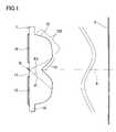
- FIG. 1is a schematic diagram of an illuminating lens according to a first embodiment of the present invention.
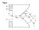
- FIG. 2is an enlarged view of the main portions of FIG. 1 .
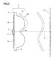
- FIG. 3is a schematic diagram of a lighting device according to a second embodiment of the present invention.
- FIG. 4is a diagram showing optical paths of light rays that reach a transmissive region of a first light exit surface of the lighting device according to the second embodiment of the present invention.
- FIG. 5is a diagram showing optical paths of light rays that reach a total reflection region of a first light exit surface of the lighting device according to the second embodiment of the present invention.
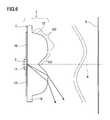
- FIG. 6is a diagram showing optical paths of light rays that exist the lighting device through a second light exit surface thereof according to the second embodiment of the present invention.
- FIG. 7is a diagram for explaining Examples 1 to 3 of the lighting device according to the second embodiment of the present invention.
- FIG. 8is a graph showing a relationship between ⁇ i and sagY, which represent the shape of the light exit surface in Example 1 of the lighting device according to the second embodiment of the present invention (i.e., a graph obtained by plotting the values in Table 1).
- FIG. 9is a graph showing a relationship between ⁇ i and sagY, which represent the shape of the light exit surface in Example 2 of the lighting device according to the second embodiment of the present invention (i.e., a graph obtained by plotting the values in Table 2).
- FIG. 10is a graph showing a relationship between ⁇ i and sagY, which represent the shape of the light exit surface in Example 3 of the lighting device according to the second embodiment of the present invention (i.e., a graph obtained by plotting the values in Table 3).
- FIG. 11is a graph showing a relationship between r/R and ⁇ i- ⁇ n in Example 1 of the lighting device according to the second embodiment of the present invention.
- FIG. 12is a graph showing a relationship between r/R and ⁇ i- ⁇ n in Example 2 of the lighting device according to the second embodiment of the present invention.
- FIG. 13is a graph showing a relationship between r/R and ⁇ i- ⁇ n in Example 3 of the lighting device according to the second embodiment of the present invention.
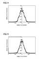
- FIG. 14shows an illuminance distribution in Example 1 of the lighting device according to the second embodiment of the present invention.
- FIG. 15shows an illuminance distribution in Example 2 of the lighting device according to the second embodiment of the present invention.
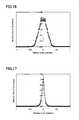
- FIG. 16shows an illuminance distribution in Example 3 of the lighting device according to the second embodiment of the present invention.
- FIG. 18is a schematic diagram of a surface light source according to a third embodiment of the present invention.
- FIG. 19is a partial cross-sectional view of the surface light source according to the third embodiment of the present invention.
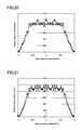
- FIG. 20shows an illuminance distribution obtained when the lighting device of Example 1 is used in the surface light source according to the third embodiment of the present invention.
- FIG. 21shows an illuminance distribution obtained when the lighting device of Example 2 is used in the surface light source according to the third embodiment of the present invention.
- FIG. 22shows an illuminance distribution obtained when the lighting device of Example 3 is used in the surface light source according to the third embodiment of the present invention.
- FIG. 23shows an illuminance distribution obtained when a surface light source including lighting devices each composed of only a light emitting diode is used to confirm the effects of Examples 1 to 3.
- FIG. 24is a schematic diagram of a liquid-crystal display apparatus according to a fourth embodiment of the present invention.
- FIG. 25is a plan view of a modified illuminating lens.
- FIG. 26A and FIG. 26Bare each a plan view of an illuminating lens of another embodiment.
- FIG. 27is a schematic diagram of an illuminating lens that has been conceived before.
- the illuminating lens 1has a light entrance surface 11 through which the light emitted from the light source enters the lens and a light exit surface 12 through which the light that has entered the lens exits the lens.
- the illuminating lens 1has a bottom surface 13 surrounding the light entrance surface 11 and facing oppositely to the light exit surface 12 .
- a radially outwardly projecting ring portion 15is provided between the light exit surface 12 and the bottom surface 13 .
- the periphery of the light exit surface 12is joined to the outer edge of the bottom surface 13 via the outer surface of the ring portion 15 having an approximately U-shaped cross section.
- the ring portion 15may be omitted.
- the periphery of the light exit surface 12may be joined to the outer edge of the bottom surface 13 with an end face having a straight or arcuate cross section.
- the light exit surface 12is axisymmetric with respect to the optical axis A.
- the contour of the illuminating lens 1 in plan viewneed not be axisymmetric with respect to the optical axis A.
- the illuminating lens 1may have an oval shape, in which the ring portion 15 has a pair of flat portions 15 a that are parallel to each other across the optical axis A, when viewed from the optical axis direction.
- the light entrance surface 11need not be axisymmetric with respect to the optical axis A.
- the region that is connected optically to the light sourceis the light entrance surface 11 .
- the annular bottom surface 13 surrounding the light entrance surface 11is flat.
- the light entrance surface 11 and the bottom surface 13are on the same level, but there may be a level difference between the light entrance surface 11 and the bottom surface 13 .
- the illuminating lens 1may be configured such that the light entrance surface 11 is located closer to the light exit surface 12 than the bottom surface 13 and the light source is fitted in the recess formed by the level difference between the surfaces 11 and 13 .
- the light entrance surface 11need not necessarily be joined directly to the light source.
- the light entrance surface 11may be recessed in a hemispherical shape so that an air space is formed between the light entrance surface 11 and the light source.
- the light emitted from the light sourceenters the illuminating lens 1 through the light entrance surface 11 , exits the lens 1 through the light exit surface 12 , and then reaches the surface to be irradiated 3 .
- the light emitted from the light sourceis spread by the action of the light exit surface 12 , and reaches a large area of the surface to be irradiated 3 .
- a light emitting diodecan be used as the light source.
- Light emitting diodesusually are chips with a rectangular plate shape. Therefore, it is preferable that the light entrance surface 11 of the illuminating lens 1 have a shape conforming to the shape of a light emitting diode to fit in close contact with the light emitting diode.
- the light emitting diodeis in contact with the light entrance surface 11 of the illuminating lens 1 via a bonding agent, and connected optically to the light entrance surface 11 .
- the light emitting diodeusually is covered with a sealing resin to avoid contact with air.
- a sealing resin for a light emitting diodean epoxy resin, silicone rubber, or the like is used.
- the illuminating lens 1is made of a transparent material having a specified refractive index.
- the refractive index of the transparent materialis, for example, about 1.4 to 1.5.
- examples of such a transparent materialinclude resins such as epoxy resin, silicone resin, acrylic resin, and polycarbonate, and rubbers such as silicone rubber. Particularly, it is preferable to use epoxy resin, silicone rubber, or the like that has been used as a sealing resin for a light emitting diode.
- the light exit surface 12includes a first light exit surface 121 that is recessed toward a point on the optical axis A, and a second light exit surface 122 extending radially outwardly from the periphery of the first light exit surface 121 to form a convex.
- the starting point Qis defined first, and then light emitted from the starting point Q is assumed.
- the starting point Qis the position of the light source on the optical axis A.
- the starting point Qis the point of intersection of the optical axis A and the light emitting surface that is the front surface of the light emitting diode. That is, the starting point Q is spaced from the light entrance surface 11 by the thickness of the above-mentioned bonding agent.
- the first light exit surface 121includes a transmissive region 123 located in the center of the first light exit surface 121 and a total reflection region 124 located around the transmissive region 123 .
- the transmissive region 123transmits light that has been emitted from the starting point Q at a relatively small angle of less than a specified value of ⁇ p with respect to the optical axis A and reached the first light exit surface 121
- the total reflection region 124totally reflects light that has been emitted from the starting point Q at a relatively large angle of ⁇ p or more with respect to the optical axis A and reached the first light exit surface 121 . That is, ⁇ p is an angle between the optical axis A and a line connecting a point P and the starting point Q, when the point P is a point on the boundary between the transparent region 123 and the total reflection region 124 .
- the second light exit surface 122has a shape capable of transmitting approximately the entire amount of light that has been emitted from the starting point Q and reached the second light exit surface 122 , and totally reflecting approximately the entire amount of the light that has been totally reflected at the total reflection region 124 and reached the second light exit surface 122 .
- the angle between the optical axis A and the light emitted from the starting point Qincreases toward the outer edge of the second light exit surface 122 .
- the angle of the light emitted from the starting point Q with respect to a normal line at the point on the second light exit surface 122 reached by the emitted lightis the incident angle of the light with respect to the second light exit surface 122 .
- An excessively large incident anglecauses total reflection.
- the second light exit surface 122has a shape such that the angle between the normal line and the optical axis A increases with increasing distance from the optical axis A. That is, the shape of the second light exit surface 122 is a convex.
- the entire second light exit surface 122need not necessarily transmit the light emitted from the starting point Q (i.e., the second light exit surface 122 need not transmit the entire amount of the light).
- the second light exit surface 122may have a shape capable of totally reflecting a part of the light emitted from the starting point Q and transmitting the remaining part of the light.
- an annular reflective layer 10is formed on the bottom surface 13 , as shown in FIG. 1 .
- the reflective layer 10has a ring shape extending radially outwardly from the optical axis A.
- the light emitted from the light sourceis totally reflected at the total reflection region 124 of the first light exit surface 121 and then reaches the second light exit surface 122 (see FIG. 5 ).
- a part of the light that has reached the second light exit surface 122passes through the second light exit surface 122 , but most of the remaining part of the light is totally reflected one or more times again at the second light exit surface 122 .
- the lighttravels along the second light exit surface 122 while being totally reflected one or more times again at the second light exit surface 122 , and then reaches the bottom surface 13 .
- the reflective layer 10reflects the light that has reached the bottom surface 13 in this way. That is, the reflective layer 10 reflects the light that has been totally reflected repeatedly at the light exit surface 12 (i.e., the total reflection region 124 of the first light exit surface 121 and the second light exit surface 122 ) and then reached the bottom surface 13 .
- the reflective layer 10may be formed of a reflective film obtained by applying a reflective material on the bottom surface 13 and curing the material.
- the reflective layer 10also may be formed of a reflective sheet attached to the bottom surface 13 .
- the reflective layer 10has a reflectance of at least 65%. This is because a reflectance of less than 65% increases the loss of light in the reflective layer 10 , which causes a decrease in irradiation efficiency and an uneven illuminance.
- the most part of the light that has been emitted from the light source and reached the transmissive region 123 located in the center of the first light exit surface 121is refracted at the transmissive region 123 , and thus the area surrounding the optical axis A of the lens on the surface to be irradiated 3 is irradiated with the refracted light.
- the most part of the light that has been emitted from the light source and reached the total reflection region 124 located on the peripheral side of the first light exit surface 121is totally reflected at the total reflection region 124 .
- the illuminating lens 1 of the present embodimentallows the range of transmission directions for light from the light source to be widened further. Therefore, the outer diameter of the lens of the present embodiment may be smaller than that of a conventional lens having a concave for only refracting light.
- the light that has reached the bottom surface 13can be guided definitely toward the surface to be irradiated 3 with a low cost configuration in which the reflective layer 10 is formed on the bottom surface 13 .
- the illuminance of the surface to be irradiated 3can be stabilized.
- the basic configuration of the illuminating lens 1 of the present embodimenthas been described so far.
- a preferable configuration of the illuminating lens 1 of the present embodimentwill be described below.
- the reflective layer 10has a circular annular shape, and satisfies the following inequalities (1) and (2).
- R inis an internal radius of the reflective layer
- R outis an outer radius of the reflective layer
- R LSis a radius of a smallest circle circumscribing the light source
- Ris an outermost radius of the illuminating lens.
- inequalities (1) and (2)define the proportion of the area of the reflective layer 10 on the bottom surface 13 , and indicate the range of proportions for controlling suitably the amount of light directed to the surface to be irradiated 3 .
- the inequality (1)when the value of R in /R is smaller than that of R LS /R, the reflective layer intrudes between the lens and the light source, which causes a decrease in the amount of light emitted from the light source.
- the reflective layeris a reflective sheet, if the diameter of the hole in the sheet is small, the sheet cannot be attached properly to the bottom surface of the lens.
- the reflective layer 10may reflect specularly the light that has reached the bottom surface 13 , but preferably, it diffusely reflects the light that has reached the bottom surface 13 . With such a configuration, the illuminance can be adjusted easily by utilizing the reflective properties of the reflective layer 10 .
- the illuminating lens of the present inventionalso is applicable to light sources (such as lasers and organic ELs) as well as light emitting diodes.
- the light exit surface 12is axisymmetric with respect to the optical axis A.
- the light exit surface 12need not be axisymmetric with respect to the optical axis A.
- the light exit surface 12may have an elliptical shape when viewed from the optical axis direction.
- This illuminating lens 1is suitable particularly for an elongated light source.
- the light exit surface 12may have a rounded rectangular shape when viewed from the optical axis direction.
- FIG. 3is a schematic diagram of a lighting device 7 according to a second embodiment of the present invention.
- This lighting device 7includes a light emitting diode 2 for emitting light, and an illuminating lens 1 of the first embodiment for spreading light emitted from the light emitting diode 2 so that the surface to be irradiated 3 is irradiated with the spread light.
- the light emitting diode 2is in contact with the light entrance surface 11 of the illuminating lens 1 via a bonding agent, and connected optically to the light entrance surface 11 .
- the light that has exited the illuminating lens 1 through the light exit surface 12reaches the surface to be irradiated 3 , and thus the surface to be irradiated 3 is illuminated with that light.
- Light generation in the light emitting diode 2has no directivity in itself, and a light emitting region has a refractive index of at least 2.0.
- the refraction of the light at the interfacecauses the light to have the maximum intensity in the normal direction of the interface and to have a lower intensity as the angle of the light with respect to the normal line increases.
- the light emitting diode 2since the light emitting diode 2 has high directivity, it is necessary to widen the range of transmission directions for light therefrom using the illuminating lens 1 to illuminate a larger area.
- FIG. 4is a diagram showing the paths of light rays in the lighting device 7 .
- the paths of light rays that are emitted from the light source at small angles and reach the transmissive region 123 (see FIG. 2 ) of the first light exit surface 121are described.
- the light that has been emitted from the light emitting diode 2passes through the light entrance surface 11 and reaches the transmissive region 123 of the first light exit surface 121 .
- the light that has reached the transmissive region 123 of the first light exit surface 121passes through the transmissive region 123 while being refracted, and then reaches the surface to be irradiated 3 .
- FIG. 5is a diagram showing the paths of light rays in the lighting device 7 .
- the paths of light rays that are emitted from the light source at small angles and reach the total reflection region 124 (see FIG. 2 ) of the first light exit surface 121are described.
- the light that has been emitted from the light emitting diode 2passes through the light entrance surface 11 and reaches the total reflection region 124 of the first light exit surface 121 .
- the light that has reached the total reflection region 124 of the first light exit surface 121is totally reflected at the total reflection region 124 .
- the light that has traveled near the optical axis Ais totally reflected to reach the second light exit surface 122 , and then passes through the second light exit surface 122 while being refracted.
- FIG. 6is a diagram showing the paths of light rays in the lighting device 7 .
- the paths of light rays that are emitted from the light source at larger angles and reach the second light exit surface 122are described.
- the light that has been emitted from the light emitting diode 2passes through the light entrance surface 11 and reaches the second light exit surface 122 .
- the second light exit surface 122does not have a shape capable of totally reflecting a part of the light, approximately the entire amount of the light that has reached the second light exit surface 122 passes through the second light exit surface 122 while being refracted, and then reaches the surface to be irradiated 3 .
- FIG. 7is a schematic diagram of a lighting device in Examples 1 to 3 according to the second embodiment of the present invention.
- Examples 1 to 3are examples of a lighting device designed to widen the range of transmission directions for light from a 0.8 mm cubic-shaped light emitting diode as a light source.
- ⁇ iis an angle between the optical axis A and a straight line connecting the position of the light source (starting point Q) on the optical axis A and an arbitrary point on the light exit surface 12 .
- starting point Qstarting point Q
- ⁇ nis an angle between the optical axis A and a normal line at the arbitrary point on the light exit surface 12 , that is, a normal line at a position on the light exit surface 12 reached by the light that has been emitted from the light source position (starting point Q) on the optical axis A at an angle of ⁇ i.
- sagYis a distance along the optical axis A between the light source position (starting point Q) on the optical axis A and the arbitrary point on the light exit surface 12 .
- FIG. 8is a graph obtained by plotting the values of ⁇ i and sagY in Table 1.
- FIG. 11is a graph showing a relationship between r/R and ⁇ i- ⁇ n.
- r/Ris a value obtained by normalizing, with respect to the outermost radius of the lens, the distance in the direction parallel to the light entrance surface 11 from the optical axis A to the arbitrary point on the light exit surface 12 , where r is the distance in the direction parallel to the light entrance surface from the optical axis to the arbitrary point on the light exit surface, and R is the outermost radius of the lens (see FIG. 7 ).
- ⁇ i- ⁇ nis an angle of a light ray emitted at an angle of ⁇ i, with respect to a normal line at a point on the light exit surface 12 reached by the light ray, that is, an incident angle of the light ray on the light exit surface 12 .
- ⁇ i- ⁇ nis 42.1 degrees or more. Accordingly, FIG. 11 shows that in Example 1, the transmissive region 123 of the first light exit surface 121 is a narrow region in the vicinity of the optical axis and the total reflection region 124 is a wide region away from the optical axis.
- FIG. 11also shows that in Example 1, the entire second light exit surface 122 totally reflects the light emitted from the starting point Q.
- Example 1R in , R out , R LS , and R shown in FIG. 7 are 4.5, 5.5, 1.41, and 6.95, respectively. Accordingly, R in /R is 0.65 and R out /R is 0.79, and these values satisfy the above inequalities (1) and (2). Furthermore, in Example 1, the reflectance of the reflective layer 10 is 67.7%.
- FIG. 14shows the illuminance distribution on the surface to be irradiated obtained by calculation assuming that the lighting device of Example 1 (i.e., the illuminating lens in FIG. 8 and the light emitting diode) is used and the surface to be irradiated is placed at a distance of 16.4 mm from the light emitting diode.
- FIG. 17shows the illuminance distribution on the surface to be irradiated obtained by calculation assuming that only the same light emitting diode as in FIG. 14 is used and the surface to be irradiated is placed at a distance of 16.4 mm from the light emitting diode.
- FIG. 17shows a curve indicating the distribution of illuminances on the surface to be irradiated when the illuminances are normalized with respect to the illuminance at the center of the optical axis being 1 .
- a comparison between FIG. 14 and FIG. 17shows that the illuminating lens is effective in increasing the illuminated area of the surface to be irradiated.
- FIG. 9is a graph obtained by plotting the values of ⁇ i and sagY in Table 2.
- FIG. 12is a graph showing a relationship between r/R and ⁇ i- ⁇ n. r/R and ⁇ i- ⁇ n in FIG. 12 are the same as those in FIG. 11 .
- Example 2the lens is made of a material having a refractive index of 1.492, as in the case of Example 1 described above. Accordingly, as a condition of the total reflection region 124 of the first light exit surface 121 , ⁇ i- ⁇ n is 42.1 degrees or more, as in the case of Example 1. Accordingly, FIG. 12 shows that in Example 2, the transmissive region 123 is as narrow as that of Example 1, and the total reflection region 124 is narrower than that of Example 1. FIG. 12 also shows that in Example 2, the second light exit surface 122 totally reflects a part of the light emitted from the starting point Q and transmits the remaining part of the light.
- Example 2R in , R out , R LS , and R shown in FIG. 7 are 2.50, 5.90, 1.41, and 6.00, respectively. Accordingly, R in /R is 0.42 and R out /R is 0.98, and these values satisfy the above inequalities (1) and (2). Furthermore, in Example 2, the reflectance of the reflective layer 10 is 97.7%.
- FIG. 15shows the illuminance distribution on the surface to be irradiated obtained by calculation assuming that the lighting device of Example 2 (i.e., the illuminating lens in FIG. 9 and the light emitting diode) is used and the surface to be irradiated is placed at a distance of 16.4 mm from the light emitting diode.
- FIG. 15shows a curve indicating the distribution of illuminances on the surface to be irradiated when the illuminances are normalized with respect to the illuminance at the center of the optical axis being 1 , as in the case of FIG. 14 .
- a comparison between FIG. 15 and FIG. 17shows that the illuminating lens is effective in increasing the illuminated area of the surface to be irradiated.
- FIG. 10is a graph obtained by plotting the values of ⁇ i and sagY in Table 3.
- FIG. 13is a graph showing a relationship between r/R and ⁇ i- ⁇ n. r/R and ⁇ i- ⁇ n in FIG. 13 are the same as those in FIG. 11 .
- Example 3the lens is made of a material having a refractive index of 1.492, as in the case of Example 1 described above. Accordingly, as a condition of the total reflection region 124 of the first light exit surface 121 , ⁇ i- ⁇ n is 42.1 degrees or more, as in the case of Example 1. Accordingly, FIG. 13 shows that in Example 3, the transmissive region 123 is as narrow as that of Example 1, and the total reflection region 124 is as wide as that of Example 1. FIG. 13 also shows that in Example 3, the entire second light exit surface 122 totally reflects the light emitted from the starting point Q.
- Example 3R in , R out , R LS , and R shown in FIG. 7 are 1.60, 6.25, 1.41, and 6.25, respectively. Accordingly, R in /R is 0.26 and R out /R is 1.00, and these values satisfy the above inequalities (1) and (2). Furthermore, in Example 3, the reflectance of the reflective layer 10 shown in FIG. 7 is 98.7%.
- FIG. 16shows the illuminance distribution on the surface to be irradiated obtained by calculation assuming that the lighting device of Example 3 (i.e., the illuminating lens in FIG. 10 and the light emitting diode) is used and the surface to be irradiated is placed at a distance of 16.4 mm from the light emitting diode.
- FIG. 16shows a curve indicating the distribution of illuminances on the surface to be irradiated when the illuminances are normalized with respect to the illuminance at the center of the optical axis being 1 , as in the case of FIG. 14 .
- a comparison between FIG. 16 and FIG. 17shows that the illuminating lens is effective in increasing the illuminated area of the surface to be irradiated.
- FIG. 18is a schematic diagram of a surface light source 9 according to a third embodiment of the present invention.
- This surface light source 9includes a plurality of lighting devices 7 of the second embodiment arranged in a plane, and a diffusing plate 4 disposed to cover the plurality of lighting devices 7 .
- the lighting devices 7may be arranged in a matrix as shown in FIG. 18 . They may be arranged in a staggered manner.
- the surface light source 9includes a substrate 8 facing the diffusing plate 4 with the lighting devices 7 being disposed therebetween. As shown in FIG. 19 , the light emitting diode 2 of each lighting device 7 is mounted on the substrate 8 . In the present embodiment, a reflecting plate 6 is disposed on the substrate 8 to cover the substrate 8 with the light emitting diodes 2 being exposed.
- the lighting device 7emits light to one surface 4 a of the diffusing plate 4 . That is, the one surface 4 a of the diffusing plate 4 is the surface to be irradiated 3 that has been described in the first and second embodiments.
- the diffusing plate 4emits the light received on its one surface 4 a from the other surface 4 b in a diffused manner.
- the lighting devices 7emit light individually toward a large area of the one surface 4 a of the diffusing plate 4 so that the one surface 4 a has a uniform illuminance, and upon receiving this light, the diffusing plate 4 emits the light diffusely. As a result, the surface light source capable of emitting light having less uneven brightness in the plane is obtained.
- the light emitted from the lighting device 7is diffused by the diffusing plate 4 so that the diffuse light returns to the lighting device side or passes through the diffusing plate 4 .
- the light that has returned to the lighting device side and struck the reflecting plate 6is reflected at the reflecting plate 6 and again enters the diffusing plate 4 .
- FIG. 20shows the illuminance distribution on the light entrance surface (one surface on the side of the lighting device) of the diffusing plate obtained by calculation assuming that five lighting devices of Example 1 each including the illuminating lens in FIG. 8 and the light emitting diode are arranged in a line at a pitch of 60 mm and the diffusing plate is placed at a distance of 16.4 mm from the light emitting diodes. Small fluctuations in the illuminance distribution are attributed to a small number of light rays to be evaluated in calculating the illuminances.
- FIG. 21 and FIG. 22show the illuminance distribution obtained in the same manner when the lighting devices of Example 2 are used and the illuminance distribution obtained when the lighting devices of Example 3 are used, respectively.
- FIG. 23shows the illuminance distribution on the light entrance surface of the diffusing plate obtained by calculation assuming that five light emitting diodes only are arranged in a line with a pitch of 60 mm and the diffusing plate is placed at a distance of 16.4 mm from the light emitting diodes.
- FIGS. 20 to 22 and FIG. 23show that the illuminating lens is effective in illuminating the light entrance surface of the diffusing plate uniformly.
- FIG. 24is a schematic diagram of a liquid-crystal display apparatus according to a fourth embodiment of the present invention.
- This liquid-crystal display apparatusincludes a liquid-crystal panel 5 , and a surface light source 9 of the third embodiment disposed behind the liquid-crystal panel 5 .
- a plurality of lighting devices 7 each including the light emitting diode 2 and the illuminating lens 1are arranged in a plane, and the diffusing plate 4 is illuminated by these lighting devices 7 .
- the underside (one surface) of the diffusing plate 4is irradiated with the light emitted from the lighting devices 7 to have a uniform illuminance, and then the light is diffused by the diffusing plate 4 .
- the liquid-crystal panel 5is illuminated by the diffused light.
- an optical sheetsuch as a diffusing sheet or a prism sheet is disposed between the liquid-crystal panel 5 and the surface light source 9 .
- the light that has passed through the diffusing plate 4further is diffused by the optical sheet and illuminates the liquid-crystal panel 5 .
Landscapes
- Physics & Mathematics (AREA)
- General Physics & Mathematics (AREA)
- Optics & Photonics (AREA)
- Nonlinear Science (AREA)
- Mathematical Physics (AREA)
- Chemical & Material Sciences (AREA)
- Crystallography & Structural Chemistry (AREA)
- Planar Illumination Modules (AREA)
Abstract
Description
RLS/R<Rin/R<0.78 (1)
0.75<Rout/R (2)
where Rinis an internal radius of the reflective layer, Routis an outer radius of the reflective layer, RLSis a radius of a smallest circle circumscribing the light source, and R is an outermost radius of the illuminating lens.
| TABLE 1 | |||
| θ i | sagY | ||
| 0.000 | 2.362 | ||
| 0.521 | 2.364 | ||
| 1.039 | 2.370 | ||
| 1.552 | 2.380 | ||
| 2.059 | 2.392 | ||
| 2.558 | 2.406 | ||
| 3.050 | 2.421 | ||
| 3.533 | 2.438 | ||
| 4.008 | 2.455 | ||
| 4.475 | 2.473 | ||
| 4.933 | 2.491 | ||
| 5.384 | 2.509 | ||
| 5.827 | 2.528 | ||
| 6.262 | 2.547 | ||
| 6.689 | 2.567 | ||
| 7.109 | 2.586 | ||
| 7.521 | 2.605 | ||
| 7.927 | 2.625 | ||
| 8.325 | 2.645 | ||
| 8.717 | 2.664 | ||
| 9.102 | 2.684 | ||
| 9.480 | 2.704 | ||
| 9.853 | 2.723 | ||
| 10.219 | 2.743 | ||
| 10.579 | 2.763 | ||
| 10.934 | 2.782 | ||
| 11.283 | 2.802 | ||
| 11.627 | 2.821 | ||
| 11.966 | 2.840 | ||
| 12.300 | 2.860 | ||
| 12.629 | 2.879 | ||
| 12.954 | 2.898 | ||
| 13.275 | 2.916 | ||
| 13.591 | 2.935 | ||
| 13.904 | 2.953 | ||
| 14.212 | 2.971 | ||
| 14.517 | 2.989 | ||
| 14.819 | 3.007 | ||
| 15.118 | 3.024 | ||
| 15.413 | 3.041 | ||
| 15.706 | 3.058 | ||
| 15.995 | 3.075 | ||
| 16.282 | 3.092 | ||
| 16.567 | 3.108 | ||
| 16.849 | 3.124 | ||
| 17.129 | 3.139 | ||
| 17.407 | 3.155 | ||
| 17.683 | 3.170 | ||
| 17.957 | 3.184 | ||
| 18.229 | 3.199 | ||
| 18.499 | 3.213 | ||
| 18.768 | 3.227 | ||
| 19.035 | 3.240 | ||
| 19.301 | 3.254 | ||
| 19.566 | 3.267 | ||
| 19.829 | 3.279 | ||
| 20.091 | 3.292 | ||
| 20.351 | 3.304 | ||
| 20.611 | 3.316 | ||
| 20.869 | 3.327 | ||
| 21.127 | 3.339 | ||
| 21.383 | 3.350 | ||
| 21.638 | 3.360 | ||
| 21.892 | 3.371 | ||
| 22.145 | 3.381 | ||
| 22.397 | 3.391 | ||
| 22.648 | 3.401 | ||
| 22.898 | 3.410 | ||
| 23.147 | 3.420 | ||
| 23.395 | 3.429 | ||
| 23.642 | 3.438 | ||
| 23.887 | 3.447 | ||
| 24.132 | 3.455 | ||
| 24.376 | 3.464 | ||
| 24.618 | 3.472 | ||
| 24.859 | 3.480 | ||
| 25.100 | 3.488 | ||
| 25.338 | 3.496 | ||
| 25.576 | 3.504 | ||
| 25.813 | 3.512 | ||
| 26.048 | 3.519 | ||
| 26.282 | 3.526 | ||
| 26.515 | 3.534 | ||
| 26.746 | 3.541 | ||
| 26.976 | 3.548 | ||
| 27.205 | 3.555 | ||
| 27.433 | 3.562 | ||
| 27.659 | 3.569 | ||
| 27.884 | 3.576 | ||
| 28.108 | 3.582 | ||
| 28.331 | 3.589 | ||
| 28.553 | 3.596 | ||
| 28.774 | 3.602 | ||
| 28.994 | 3.608 | ||
| 29.213 | 3.614 | ||
| 29.431 | 3.620 | ||
| 29.649 | 3.626 | ||
| 29.867 | 3.632 | ||
| 30.084 | 3.637 | ||
| 30.301 | 3.642 | ||
| 30.519 | 3.647 | ||
| 30.737 | 3.652 | ||
| 30.955 | 3.656 | ||
| 31.175 | 3.660 | ||
| 31.395 | 3.664 | ||
| 31.618 | 3.667 | ||
| 31.842 | 3.670 | ||
| 32.069 | 3.672 | ||
| 32.298 | 3.673 | ||
| 32.531 | 3.674 | ||
| 32.767 | 3.674 | ||
| 33.008 | 3.674 | ||
| 33.253 | 3.672 | ||
| 33.504 | 3.670 | ||
| 33.762 | 3.667 | ||
| 33.953 | 3.672 | ||
| 34.176 | 3.673 | ||
| 34.397 | 3.674 | ||
| 34.616 | 3.675 | ||
| 34.833 | 3.677 | ||
| 35.048 | 3.678 | ||
| 35.261 | 3.679 | ||
| 35.473 | 3.681 | ||
| 35.684 | 3.682 | ||
| 35.892 | 3.684 | ||
| 36.100 | 3.685 | ||
| 36.306 | 3.687 | ||
| 36.511 | 3.689 | ||
| 36.715 | 3.690 | ||
| 36.918 | 3.692 | ||
| 37.120 | 3.693 | ||
| 37.321 | 3.694 | ||
| 37.521 | 3.696 | ||
| 37.720 | 3.697 | ||
| 37.919 | 3.698 | ||
| 38.117 | 3.699 | ||
| 38.315 | 3.700 | ||
| 38.512 | 3.701 | ||
| 38.708 | 3.702 | ||
| 38.905 | 3.703 | ||
| 39.101 | 3.704 | ||
| 39.296 | 3.704 | ||
| 39.492 | 3.705 | ||
| 39.687 | 3.705 | ||
| 39.882 | 3.705 | ||
| 40.077 | 3.705 | ||
| 40.273 | 3.705 | ||
| 40.468 | 3.705 | ||
| 40.663 | 3.704 | ||
| 40.858 | 3.704 | ||
| 41.053 | 3.703 | ||
| 41.249 | 3.702 | ||
| 41.444 | 3.701 | ||
| 41.640 | 3.700 | ||
| 41.836 | 3.698 | ||
| 42.032 | 3.697 | ||
| 42.229 | 3.695 | ||
| 42.425 | 3.693 | ||
| 42.622 | 3.691 | ||
| 42.819 | 3.689 | ||
| 43.017 | 3.687 | ||
| 43.214 | 3.684 | ||
| 43.412 | 3.682 | ||
| 43.611 | 3.679 | ||
| 43.809 | 3.676 | ||
| 44.008 | 3.673 | ||
| 44.207 | 3.669 | ||
| 44.406 | 3.666 | ||
| 44.606 | 3.662 | ||
| 44.805 | 3.658 | ||
| 45.005 | 3.654 | ||
| 45.205 | 3.650 | ||
| 45.406 | 3.646 | ||
| 45.606 | 3.642 | ||
| 45.807 | 3.637 | ||
| 46.008 | 3.632 | ||
| 46.209 | 3.628 | ||
| 46.410 | 3.623 | ||
| 46.611 | 3.618 | ||
| 46.813 | 3.612 | ||
| 47.014 | 3.607 | ||
| 47.216 | 3.602 | ||
| 47.418 | 3.596 | ||
| 47.6193 | 3.590 | ||
| 47.8210 | 3.584 | ||
| 48.0228 | 3.578 | ||
| 48.2246 | 3.572 | ||
| 48.4264 | 3.566 | ||
| 48.6282 | 3.560 | ||
| 48.8301 | 3.554 | ||
| 49.0319 | 3.547 | ||
| 49.2337 | 3.540 | ||
| 49.4355 | 3.534 | ||
| 49.6372 | 3.527 | ||
| 49.8390 | 3.520 | ||
| 50.0408 | 3.513 | ||
| 50.2425 | 3.506 | ||
| 50.4443 | 3.498 | ||
| 50.6460 | 3.491 | ||
| 50.8478 | 3.484 | ||
| 51.0496 | 3.476 | ||
| 51.2515 | 3.468 | ||
| 51.4534 | 3.460 | ||
| 51.6554 | 3.452 | ||
| 51.8575 | 3.444 | ||
| 52.0596 | 3.436 | ||
| 52.2620 | 3.428 | ||
| 52.4644 | 3.419 | ||
| 52.6671 | 3.411 | ||
| 52.8700 | 3.402 | ||
| 53.0731 | 3.393 | ||
| 53.2765 | 3.384 | ||
| 53.4802 | 3.375 | ||
| 53.6842 | 3.366 | ||
| 53.8886 | 3.357 | ||
| 54.0933 | 3.347 | ||
| 54.2985 | 3.337 | ||
| 54.5042 | 3.327 | ||
| 54.7104 | 3.317 | ||
| 54.9171 | 3.307 | ||
| 55.1244 | 3.297 | ||
| 55.3323 | 3.286 | ||
| 55.5409 | 3.275 | ||
| 55.7501 | 3.264 | ||
| 55.9601 | 3.253 | ||
| 56.1708 | 3.242 | ||
| 56.3823 | 3.230 | ||
| 56.5947 | 3.219 | ||
| 56.8079 | 3.207 | ||
| 57.0220 | 3.195 | ||
| 57.2370 | 3.182 | ||
| 57.4530 | 3.170 | ||
| 57.6700 | 3.157 | ||
| 57.8879 | 3.144 | ||
| 58.1070 | 3.131 | ||
| 58.3271 | 3.117 | ||
| 58.5483 | 3.103 | ||
| 58.7706 | 3.090 | ||
| 58.9941 | 3.075 | ||
| 59.2187 | 3.061 | ||
| 59.4445 | 3.046 | ||
| 59.6716 | 3.031 | ||
| 59.8998 | 3.016 | ||
| 60.1294 | 3.001 | ||
| 60.360 | 2.985 | ||
| 60.592 | 2.969 | ||
| 60.826 | 2.953 | ||
| 61.061 | 2.936 | ||
| 61.297 | 2.920 | ||
| 61.534 | 2.903 | ||
| 61.773 | 2.885 | ||
| 62.014 | 2.868 | ||
| 62.256 | 2.850 | ||
| 62.500 | 2.832 | ||
| 62.745 | 2.813 | ||
| 62.993 | 2.794 | ||
| 63.242 | 2.775 | ||
| 63.493 | 2.756 | ||
| 63.746 | 2.736 | ||
| 64.002 | 2.716 | ||
| 64.260 | 2.695 | ||
| 64.520 | 2.674 | ||
| 64.784 | 2.653 | ||
| 65.050 | 2.631 | ||
| 65.320 | 2.608 | ||
| 65.594 | 2.585 | ||
| 65.871 | 2.562 | ||
| 66.153 | 2.537 | ||
| 66.279 | 2.527 | ||
| 66.659 | 2.493 | ||
| 66.872 | 2.475 | ||
| 67.134 | 2.451 | ||
| 67.401 | 2.427 | ||
| 67.673 | 2.402 | ||
| 67.951 | 2.377 | ||
| 68.236 | 2.350 | ||
| 68.529 | 2.323 | ||
| 68.829 | 2.295 | ||
| 69.138 | 2.265 | ||
| 69.456 | 2.234 | ||
| 69.785 | 2.202 | ||
| 70.125 | 2.169 | ||
| 70.477 | 2.134 | ||
| 70.843 | 2.097 | ||
| 71.223 | 2.059 | ||
| 71.619 | 2.018 | ||
| 72.033 | 1.976 | ||
| 72.465 | 1.931 | ||
| 72.917 | 1.884 | ||
| 73.392 | 1.834 | ||
| 73.891 | 1.781 | ||
| 74.415 | 1.725 | ||
| 74.968 | 1.666 | ||
| 75.552 | 1.604 | ||
| 76.169 | 1.537 | ||
| 76.821 | 1.466 | ||
| 77.512 | 1.391 | ||
| 78.245 | 1.311 | ||
| 79.023 | 1.225 | ||
| 79.850 | 1.134 | ||
| TABLE 2 | |||
| θ i | sagY | ||
| 0.000 | 1.842 | ||
| 0.668 | 1.844 | ||
| 1.332 | 1.849 | ||
| 1.989 | 1.857 | ||
| 2.635 | 1.868 | ||
| 3.269 | 1.882 | ||
| 3.886 | 1.899 | ||
| 4.487 | 1.918 | ||
| 5.071 | 1.938 | ||
| 5.636 | 1.961 | ||
| 6.182 | 1.985 | ||
| 6.711 | 2.010 | ||
| 7.221 | 2.036 | ||
| 7.715 | 2.063 | ||
| 8.192 | 2.091 | ||
| 8.654 | 2.119 | ||
| 9.100 | 2.148 | ||
| 9.533 | 2.176 | ||
| 9.953 | 2.205 | ||
| 10.361 | 2.234 | ||
| 10.757 | 2.263 | ||
| 11.143 | 2.292 | ||
| 11.519 | 2.321 | ||
| 11.886 | 2.349 | ||
| 12.245 | 2.378 | ||
| 12.596 | 2.405 | ||
| 12.940 | 2.433 | ||
| 13.278 | 2.460 | ||
| 13.609 | 2.487 | ||
| 13.935 | 2.513 | ||
| 14.256 | 2.539 | ||
| 14.572 | 2.564 | ||
| 14.884 | 2.589 | ||
| 15.193 | 2.613 | ||
| 15.497 | 2.636 | ||
| 15.799 | 2.659 | ||
| 16.098 | 2.682 | ||
| 16.394 | 2.704 | ||
| 16.688 | 2.725 | ||
| 16.980 | 2.746 | ||
| 17.270 | 2.766 | ||
| 17.558 | 2.786 | ||
| 17.845 | 2.805 | ||
| 18.130 | 2.823 | ||
| 18.415 | 2.841 | ||
| 18.698 | 2.859 | ||
| 18.981 | 2.875 | ||
| 19.262 | 2.892 | ||
| 19.543 | 2.907 | ||
| 19.824 | 2.922 | ||
| 20.104 | 2.937 | ||
| 20.384 | 2.951 | ||
| 20.663 | 2.964 | ||
| 20.942 | 2.977 | ||
| 21.221 | 2.990 | ||
| 21.500 | 3.002 | ||
| 21.778 | 3.014 | ||
| 22.056 | 3.025 | ||
| 22.334 | 3.035 | ||
| 22.613 | 3.046 | ||
| 22.890 | 3.055 | ||
| 23.168 | 3.065 | ||
| 23.446 | 3.074 | ||
| 23.723 | 3.082 | ||
| 24.001 | 3.090 | ||
| 24.278 | 3.098 | ||
| 24.554 | 3.106 | ||
| 24.831 | 3.113 | ||
| 25.107 | 3.120 | ||
| 25.383 | 3.127 | ||
| 25.658 | 3.133 | ||
| 25.933 | 3.139 | ||
| 26.208 | 3.145 | ||
| 26.482 | 3.150 | ||
| 26.755 | 3.156 | ||
| 27.027 | 3.161 | ||
| 27.299 | 3.166 | ||
| 27.570 | 3.171 | ||
| 27.840 | 3.175 | ||
| 28.109 | 3.180 | ||
| 28.377 | 3.184 | ||
| 28.644 | 3.188 | ||
| 28.910 | 3.192 | ||
| 29.175 | 3.196 | ||
| 29.438 | 3.200 | ||
| 29.700 | 3.204 | ||
| 29.960 | 3.208 | ||
| 30.220 | 3.211 | ||
| 30.477 | 3.215 | ||
| 30.733 | 3.218 | ||
| 30.988 | 3.222 | ||
| 31.241 | 3.225 | ||
| 31.492 | 3.229 | ||
| 31.741 | 3.232 | ||
| 31.989 | 3.236 | ||
| 32.235 | 3.239 | ||
| 32.479 | 3.242 | ||
| 32.721 | 3.246 | ||
| 32.961 | 3.249 | ||
| 33.200 | 3.253 | ||
| 33.437 | 3.256 | ||
| 33.672 | 3.260 | ||
| 33.905 | 3.263 | ||
| 34.137 | 3.266 | ||
| 34.366 | 3.270 | ||
| 34.594 | 3.273 | ||
| 34.821 | 3.277 | ||
| 35.046 | 3.280 | ||
| 35.269 | 3.283 | ||
| 35.491 | 3.287 | ||
| 35.712 | 3.290 | ||
| 35.931 | 3.293 | ||
| 36.150 | 3.296 | ||
| 36.367 | 3.299 | ||
| 36.583 | 3.302 | ||
| 36.799 | 3.305 | ||
| 37.014 | 3.308 | ||
| 37.229 | 3.311 | ||
| 37.443 | 3.313 | ||
| 37.657 | 3.315 | ||
| 37.872 | 3.318 | ||
| 38.086 | 3.319 | ||
| 38.301 | 3.321 | ||
| 38.517 | 3.323 | ||
| 38.734 | 3.324 | ||
| 38.962 | 3.323 | ||
| 39.213 | 3.320 | ||
| 39.461 | 3.317 | ||
| 39.708 | 3.314 | ||
| 39.952 | 3.311 | ||
| 40.194 | 3.308 | ||
| 40.434 | 3.305 | ||
| 40.672 | 3.303 | ||
| 40.909 | 3.300 | ||
| 41.144 | 3.297 | ||
| 41.377 | 3.295 | ||
| 41.609 | 3.292 | ||
| 41.839 | 3.290 | ||
| 42.068 | 3.287 | ||
| 42.295 | 3.285 | ||
| 42.521 | 3.282 | ||
| 42.747 | 3.280 | ||
| 42.971 | 3.277 | ||
| 43.194 | 3.275 | ||
| 43.416 | 3.272 | ||
| 43.637 | 3.269 | ||
| 43.858 | 3.267 | ||
| 44.078 | 3.264 | ||
| 44.297 | 3.261 | ||
| 44.516 | 3.258 | ||
| 44.735 | 3.255 | ||
| 44.953 | 3.252 | ||
| 45.171 | 3.249 | ||
| 45.389 | 3.245 | ||
| 45.606 | 3.242 | ||
| 45.824 | 3.238 | ||
| 46.041 | 3.234 | ||
| 46.259 | 3.230 | ||
| 46.476 | 3.226 | ||
| 46.694 | 3.222 | ||
| 46.912 | 3.218 | ||
| 47.131 | 3.213 | ||
| 47.350 | 3.208 | ||
| 47.569 | 3.204 | ||
| 47.789 | 3.198 | ||
| 48.009 | 3.193 | ||
| 48.230 | 3.188 | ||
| 48.451 | 3.182 | ||
| 48.673 | 3.176 | ||
| 48.896 | 3.170 | ||
| 49.119 | 3.164 | ||
| 49.343 | 3.157 | ||
| 49.568 | 3.151 | ||
| 49.794 | 3.144 | ||
| 50.020 | 3.137 | ||
| 50.248 | 3.129 | ||
| 50.476 | 3.122 | ||
| 50.705 | 3.114 | ||
| 50.935 | 3.106 | ||
| 51.166 | 3.098 | ||
| 51.399 | 3.090 | ||
| 51.632 | 3.081 | ||
| 51.865 | 3.072 | ||
| 52.1004 | 3.063 | ||
| 52.3363 | 3.054 | ||
| 52.5733 | 3.044 | ||
| 52.8112 | 3.034 | ||
| 53.0501 | 3.024 | ||
| 53.2900 | 3.014 | ||
| 53.5309 | 3.003 | ||
| 53.7728 | 2.993 | ||
| 54.0156 | 2.982 | ||
| 54.2595 | 2.971 | ||
| 54.5043 | 2.959 | ||
| 54.7501 | 2.948 | ||
| 54.9969 | 2.936 | ||
| 55.2447 | 2.924 | ||
| 55.4934 | 2.912 | ||
| 55.7430 | 2.899 | ||
| 55.9937 | 2.887 | ||
| 56.2453 | 2.874 | ||
| 56.4978 | 2.861 | ||
| 56.7513 | 2.847 | ||
| 57.0057 | 2.834 | ||
| 57.2612 | 2.820 | ||
| 57.5176 | 2.806 | ||
| 57.7750 | 2.792 | ||
| 58.0334 | 2.777 | ||
| 58.2928 | 2.763 | ||
| 58.5533 | 2.748 | ||
| 58.8149 | 2.733 | ||
| 59.0776 | 2.717 | ||
| 59.3416 | 2.702 | ||
| 59.6067 | 2.686 | ||
| 59.8731 | 2.670 | ||
| 60.1409 | 2.654 | ||
| 60.4101 | 2.637 | ||
| 60.6809 | 2.620 | ||
| 60.9533 | 2.603 | ||
| 61.2274 | 2.586 | ||
| 61.5035 | 2.568 | ||
| 61.7815 | 2.550 | ||
| 62.0618 | 2.531 | ||
| 62.3444 | 2.512 | ||
| 62.6296 | 2.493 | ||
| 62.9175 | 2.474 | ||
| 63.2085 | 2.454 | ||
| 63.5027 | 2.433 | ||
| 63.8006 | 2.412 | ||
| 64.1023 | 2.390 | ||
| 64.4083 | 2.368 | ||
| 64.7190 | 2.346 | ||
| 65.0347 | 2.322 | ||
| 65.3559 | 2.298 | ||
| 65.6831 | 2.273 | ||
| 66.0169 | 2.248 | ||
| 66.3578 | 2.221 | ||
| 66.7066 | 2.194 | ||
| 67.0639 | 2.165 | ||
| 67.4304 | 2.136 | ||
| 67.8071 | 2.105 | ||
| 68.1948 | 2.073 | ||
| 68.5945 | 2.040 | ||
| 69.0072 | 2.005 | ||
| 69.434 | 1.968 | ||
| 69.877 | 1.930 | ||
| 70.336 | 1.890 | ||
| 70.813 | 1.848 | ||
| 71.311 | 1.804 | ||
| 71.830 | 1.757 | ||
| 72.372 | 1.708 | ||
| 72.940 | 1.656 | ||
| 73.536 | 1.601 | ||
| 74.161 | 1.543 | ||
| 74.819 | 1.482 | ||
| 75.512 | 1.417 | ||
| 76.243 | 1.348 | ||
| 77.015 | 1.274 | ||
| 77.832 | 1.196 | ||
| 78.696 | 1.113 | ||
| 79.613 | 1.025 | ||
| TABLE 3 | |||
| θ i | sagY | ||
| 0.000 | 2.411 | ||
| 0.510 | 2.413 | ||
| 1.018 | 2.420 | ||
| 1.520 | 2.431 | ||
| 2.016 | 2.443 | ||
| 2.504 | 2.458 | ||
| 2.985 | 2.473 | ||
| 3.459 | 2.490 | ||
| 3.925 | 2.507 | ||
| 4.384 | 2.524 | ||
| 4.835 | 2.542 | ||
| 5.279 | 2.559 | ||
| 5.716 | 2.578 | ||
| 6.146 | 2.596 | ||
| 6.569 | 2.614 | ||
| 6.985 | 2.632 | ||
| 7.394 | 2.651 | ||
| 7.797 | 2.669 | ||
| 8.193 | 2.688 | ||
| 8.584 | 2.706 | ||
| 8.968 | 2.725 | ||
| 9.347 | 2.743 | ||
| 9.720 | 2.761 | ||
| 10.088 | 2.779 | ||
| 10.451 | 2.798 | ||
| 10.808 | 2.815 | ||
| 11.161 | 2.833 | ||
| 11.509 | 2.851 | ||
| 11.853 | 2.868 | ||
| 12.192 | 2.886 | ||
| 12.527 | 2.903 | ||
| 12.859 | 2.920 | ||
| 13.186 | 2.936 | ||
| 13.510 | 2.953 | ||
| 13.831 | 2.969 | ||
| 14.149 | 2.985 | ||
| 14.463 | 3.001 | ||
| 14.775 | 3.016 | ||
| 15.084 | 3.031 | ||
| 15.390 | 3.046 | ||
| 15.693 | 3.061 | ||
| 15.995 | 3.075 | ||
| 16.294 | 3.089 | ||
| 16.591 | 3.103 | ||
| 16.885 | 3.117 | ||
| 17.178 | 3.130 | ||
| 17.469 | 3.143 | ||
| 17.758 | 3.155 | ||
| 18.045 | 3.168 | ||
| 18.331 | 3.180 | ||
| 18.615 | 3.192 | ||
| 18.897 | 3.203 | ||
| 19.177 | 3.215 | ||
| 19.457 | 3.226 | ||
| 19.734 | 3.236 | ||
| 20.010 | 3.247 | ||
| 20.284 | 3.258 | ||
| 20.557 | 3.268 | ||
| 20.829 | 3.278 | ||
| 21.099 | 3.288 | ||
| 21.367 | 3.297 | ||
| 21.633 | 3.307 | ||
| 21.898 | 3.316 | ||
| 22.162 | 3.325 | ||
| 22.424 | 3.335 | ||
| 22.684 | 3.343 | ||
| 22.942 | 3.352 | ||
| 23.199 | 3.361 | ||
| 23.454 | 3.370 | ||
| 23.708 | 3.378 | ||
| 23.959 | 3.387 | ||
| 24.209 | 3.395 | ||
| 24.457 | 3.403 | ||
| 24.704 | 3.412 | ||
| 24.949 | 3.420 | ||
| 25.192 | 3.428 | ||
| 25.434 | 3.436 | ||
| 25.674 | 3.444 | ||
| 25.913 | 3.452 | ||
| 26.150 | 3.459 | ||
| 26.387 | 3.467 | ||
| 26.622 | 3.474 | ||
| 26.857 | 3.482 | ||
| 27.090 | 3.489 | ||
| 27.324 | 3.496 | ||
| 27.557 | 3.502 | ||
| 27.790 | 3.508 | ||
| 28.024 | 3.514 | ||
| 28.258 | 3.520 | ||
| 28.494 | 3.525 | ||
| 28.731 | 3.530 | ||
| 28.970 | 3.534 | ||
| 29.212 | 3.537 | ||
| 29.457 | 3.540 | ||
| 29.705 | 3.542 | ||
| 29.959 | 3.544 | ||
| 30.198 | 3.547 | ||
| 30.453 | 3.547 | ||
| 30.704 | 3.548 | ||
| 30.953 | 3.549 | ||
| 31.199 | 3.550 | ||
| 31.443 | 3.552 | ||
| 31.684 | 3.553 | ||
| 31.923 | 3.555 | ||
| 32.160 | 3.556 | ||
| 32.394 | 3.558 | ||
| 32.627 | 3.560 | ||
| 32.857 | 3.562 | ||
| 33.086 | 3.564 | ||
| 33.313 | 3.566 | ||
| 33.538 | 3.568 | ||
| 33.762 | 3.570 | ||
| 33.985 | 3.572 | ||
| 34.205 | 3.574 | ||
| 34.425 | 3.576 | ||
| 34.644 | 3.578 | ||
| 34.861 | 3.580 | ||
| 35.078 | 3.582 | ||
| 35.293 | 3.584 | ||
| 35.508 | 3.586 | ||
| 35.721 | 3.588 | ||
| 35.935 | 3.589 | ||
| 36.147 | 3.591 | ||
| 36.359 | 3.592 | ||
| 36.570 | 3.594 | ||
| 36.781 | 3.595 | ||
| 36.992 | 3.596 | ||
| 37.202 | 3.597 | ||
| 37.412 | 3.598 | ||
| 37.622 | 3.599 | ||
| 37.831 | 3.599 | ||
| 38.040 | 3.600 | ||
| 38.250 | 3.600 | ||
| 38.459 | 3.600 | ||
| 38.668 | 3.600 | ||
| 38.877 | 3.600 | ||
| 39.085 | 3.600 | ||
| 39.294 | 3.599 | ||
| 39.503 | 3.599 | ||
| 39.712 | 3.598 | ||
| 39.921 | 3.597 | ||
| 40.130 | 3.596 | ||
| 40.339 | 3.595 | ||
| 40.549 | 3.594 | ||
| 40.758 | 3.592 | ||
| 40.967 | 3.590 | ||
| 41.176 | 3.589 | ||
| 41.386 | 3.587 | ||
| 41.595 | 3.585 | ||
| 41.804 | 3.582 | ||
| 42.014 | 3.580 | ||
| 42.223 | 3.577 | ||
| 42.433 | 3.575 | ||
| 42.642 | 3.572 | ||
| 42.852 | 3.569 | ||
| 43.061 | 3.566 | ||
| 43.270 | 3.563 | ||
| 43.480 | 3.560 | ||
| 43.689 | 3.556 | ||
| 43.898 | 3.553 | ||
| 44.107 | 3.549 | ||
| 44.316 | 3.545 | ||
| 44.525 | 3.541 | ||
| 44.734 | 3.537 | ||
| 44.943 | 3.533 | ||
| 45.152 | 3.529 | ||
| 45.361 | 3.524 | ||
| 45.569 | 3.520 | ||
| 45.778 | 3.515 | ||
| 45.986 | 3.511 | ||
| 46.194 | 3.506 | ||
| 46.403 | 3.501 | ||
| 46.611 | 3.496 | ||
| 46.819 | 3.491 | ||
| 47.027 | 3.485 | ||
| 47.235 | 3.480 | ||
| 47.443 | 3.474 | ||
| 47.652 | 3.469 | ||
| 47.860 | 3.463 | ||
| 48.068 | 3.457 | ||
| 48.277 | 3.451 | ||
| 48.486 | 3.445 | ||
| 48.695 | 3.438 | ||
| 48.9038 | 3.432 | ||
| 49.1133 | 3.425 | ||
| 49.3230 | 3.418 | ||
| 49.5332 | 3.411 | ||
| 49.7437 | 3.404 | ||
| 49.9546 | 3.397 | ||
| 50.1661 | 3.390 | ||
| 50.3781 | 3.382 | ||
| 50.5906 | 3.374 | ||
| 50.8038 | 3.366 | ||
| 51.0177 | 3.358 | ||
| 51.2322 | 3.350 | ||
| 51.4476 | 3.341 | ||
| 51.6637 | 3.332 | ||
| 51.8807 | 3.323 | ||
| 52.0986 | 3.314 | ||
| 52.3174 | 3.305 | ||
| 52.5372 | 3.295 | ||
| 52.7580 | 3.285 | ||
| 52.9799 | 3.275 | ||
| 53.2029 | 3.265 | ||
| 53.4269 | 3.254 | ||
| 53.6521 | 3.243 | ||
| 53.8785 | 3.232 | ||
| 54.1061 | 3.221 | ||
| 54.3349 | 3.209 | ||
| 54.5649 | 3.198 | ||
| 54.7961 | 3.185 | ||
| 55.0286 | 3.173 | ||
| 55.2624 | 3.161 | ||
| 55.4974 | 3.148 | ||
| 55.7336 | 3.135 | ||
| 55.9711 | 3.121 | ||
| 56.2099 | 3.108 | ||
| 56.4498 | 3.094 | ||
| 56.6910 | 3.080 | ||
| 56.9333 | 3.066 | ||
| 57.1768 | 3.051 | ||
| 57.4214 | 3.036 | ||
| 57.6672 | 3.021 | ||
| 57.9140 | 3.006 | ||
| 58.1618 | 2.990 | ||
| 58.4107 | 2.975 | ||
| 58.6605 | 2.959 | ||
| 58.9113 | 2.943 | ||
| 59.1630 | 2.926 | ||
| 59.4156 | 2.910 | ||
| 59.6691 | 2.893 | ||
| 59.9234 | 2.876 | ||
| 60.1786 | 2.859 | ||
| 60.4346 | 2.842 | ||
| 60.6914 | 2.824 | ||
| 60.9492 | 2.807 | ||
| 61.2078 | 2.789 | ||
| 61.4673 | 2.770 | ||
| 61.7278 | 2.752 | ||
| 61.9894 | 2.733 | ||
| 62.2523 | 2.715 | ||
| 62.5164 | 2.695 | ||
| 62.7819 | 2.676 | ||
| 63.0492 | 2.656 | ||
| 63.318 | 2.636 | ||
| 63.590 | 2.616 | ||
| 63.863 | 2.595 | ||
| 64.140 | 2.574 | ||
| 64.419 | 2.552 | ||
| 64.702 | 2.530 | ||
| 64.990 | 2.508 | ||
| 65.282 | 2.484 | ||
| 65.579 | 2.460 | ||
| 65.883 | 2.435 | ||
| 66.193 | 2.409 | ||
| 66.511 | 2.383 | ||
| 66.838 | 2.355 | ||
| 67.175 | 2.326 | ||
| 67.522 | 2.295 | ||
| 67.882 | 2.263 | ||
| 68.256 | 2.229 | ||
| 68.646 | 2.194 | ||
| 69.052 | 2.156 | ||
| 69.478 | 2.117 | ||
| 69.926 | 2.074 | ||
| 70.397 | 2.029 | ||
| 70.894 | 1.981 | ||
| 71.420 | 1.930 | ||
| 71.979 | 1.875 | ||
| 72.573 | 1.815 | ||
| 73.206 | 1.752 | ||
| 73.881 | 1.684 | ||
| 74.605 | 1.610 | ||
| 75.380 | 1.531 | ||
| 76.212 | 1.446 | ||
| 77.106 | 1.353 | ||
| 78.069 | 1.254 | ||
| 79.105 | 1.146 | ||
| 80.223 | 1.030 | ||
Claims (14)
RLS/R<Rin/R<0.78
0.75<Rout/R
Applications Claiming Priority (4)
| Application Number | Priority Date | Filing Date | Title |
|---|---|---|---|
| JP2009-029350 | 2009-02-12 | ||
| JP2009029350 | 2009-02-12 | ||
| JP2009-146767 | 2009-06-19 | ||
| JP2009146767AJP5342938B2 (en) | 2009-06-19 | 2009-06-19 | Lighting lens, light emitting device, surface light source, and liquid crystal display device |
Publications (2)
| Publication Number | Publication Date |
|---|---|
| US20100201910A1 US20100201910A1 (en) | 2010-08-12 |
| US8558967B2true US8558967B2 (en) | 2013-10-15 |
Family
ID=42540158
Family Applications (1)
| Application Number | Title | Priority Date | Filing Date |
|---|---|---|---|
| US12/704,813Active - Reinstated2031-04-18US8558967B2 (en) | 2009-02-12 | 2010-02-12 | Illuminating lens, lighting device, surface light source, and liquid-crystal display apparatus |
Country Status (1)
| Country | Link |
|---|---|
| US (1) | US8558967B2 (en) |
Cited By (6)
| Publication number | Priority date | Publication date | Assignee | Title |
|---|---|---|---|---|
| US20140009944A1 (en)* | 2012-07-04 | 2014-01-09 | Enplas Corporation | Light flux controlling member, light emitting apparatus, surface light source apparatus, and display apparatus |
| US20140376219A1 (en)* | 2011-03-25 | 2014-12-25 | Sharp Kabushiki Kaisha | Light-emitting device, illuminating apparatus, and display apparatus |
| US20150268513A1 (en)* | 2014-03-24 | 2015-09-24 | Samsung Display Co., Ltd. | Light source module, backlight assembly, and display device including the same |
| US20180059484A1 (en)* | 2016-08-31 | 2018-03-01 | Mitsubishi Electric Corporation | Surface light source apparatus and liquid crystal display |
| US11199307B2 (en)* | 2017-02-28 | 2021-12-14 | Seoul Semiconductor Co., Ltd. | Display device, backlight unit, light emitting module and lens |
| US11242977B2 (en)* | 2017-07-26 | 2022-02-08 | Lumileds Llc | Illumination device with element having annular coating |
Families Citing this family (3)
| Publication number | Priority date | Publication date | Assignee | Title |
|---|---|---|---|---|
| JP5236521B2 (en)* | 2009-02-19 | 2013-07-17 | 株式会社ジャパンディスプレイイースト | Liquid crystal display |
| US20130088877A1 (en)* | 2011-10-07 | 2013-04-11 | Lextar Electronics Corporation | Lighting device and component |
| KR102240756B1 (en)* | 2014-06-30 | 2021-04-15 | 현대모비스 주식회사 | Lamp design method for automobile |
Citations (37)
| Publication number | Priority date | Publication date | Assignee | Title |
|---|---|---|---|---|
| JP2004087411A (en) | 2002-08-29 | 2004-03-18 | Toyoda Gosei Co Ltd | Lamp |
| US20040246606A1 (en)* | 2002-10-11 | 2004-12-09 | Pablo Benitez | Compact folded-optics illumination lens |
| US20040257826A1 (en) | 2003-06-19 | 2004-12-23 | Koito Manufacturing Co., Ltd | Lamp unit and vehicle headlamp using the same |
| US20050243577A1 (en) | 2004-04-29 | 2005-11-03 | Moon Jeong M | LED lamp unit |
| JP2006005791A (en) | 2004-06-18 | 2006-01-05 | Tokyo Univ Of Science | Channel estimation and data detection method |
| JP2006113556A (en) | 2004-10-15 | 2006-04-27 | Samsung Electro Mech Co Ltd | LED light source lens |
| KR20060040502A (en) | 2004-11-06 | 2006-05-10 | 럭스피아 주식회사 | Light emitting unit and backlight device employing the same |
| US20060109669A1 (en) | 2004-11-24 | 2006-05-25 | Koito Manufacturing Co., Ltd. | Vehicle lighting device |
| US20060119250A1 (en) | 2001-11-16 | 2006-06-08 | Yoshinobu Suehiro | Light-emitting diode, led light, and light apparatus |
| US20060126343A1 (en)* | 2004-12-15 | 2006-06-15 | Min-Hsun Hsieh | LED light source |
| US20060152932A1 (en) | 2005-01-12 | 2006-07-13 | Au Optronics Corp. | Dish lens for backlight module and light emitting diode |
| JP2006252841A (en) | 2005-03-09 | 2006-09-21 | Koito Ind Ltd | Beacon light |
| US20060239020A1 (en) | 2005-04-21 | 2006-10-26 | Valeo Vision | Lighting module giving a light beam with cut-off line for a motor vehicle headlight, and a headlight comprising such a module |
| JP2006309242A (en) | 2005-04-26 | 2006-11-09 | Lg Electronics Inc | Optical lens and light emitting device package and backlight unit using the same |
| JP3875247B2 (en) | 2004-09-27 | 2007-01-31 | 株式会社エンプラス | Light emitting device, surface light source device, display device, and light flux controlling member |
| JP2007026702A (en) | 2005-07-12 | 2007-02-01 | Nitto Denko Corp | Direct type backlight |
| US20070029563A1 (en) | 2005-08-05 | 2007-02-08 | Koito Manufacturing Co., Ltd. | Light-emitting diode and vehicular lamp |
| JP2007034307A (en) | 2005-07-26 | 2007-02-08 | Samsung Electronics Co Ltd | Optical lens and optical package, backlight assembly and display device having the same, and method of emitting uniform light from backlight assembly including point light source but omitting light guide |
| WO2007021149A1 (en) | 2005-08-19 | 2007-02-22 | Lg Chem, Ltd. | Side emitting lens, light emitting device using the side emitting lens, mold assembly for preparing the side emitting lens and method for preparing the side emitting lens |
| US20070047232A1 (en) | 2005-08-30 | 2007-03-01 | Samsung Electro-Mechanics Co., Ltd. | Led lens for backlight |
| US20070070530A1 (en)* | 2005-09-27 | 2007-03-29 | Seo Jung H | Light emitting device package and backlight unit using the same |
| JP2007102139A (en) | 2004-12-03 | 2007-04-19 | Sony Corp | Light pickup lens, light emitting element assembly, surface light source device, and color liquid crystal display unit assembly |
| JP2007287479A (en) | 2006-04-17 | 2007-11-01 | Sharp Corp | LIGHTING DEVICE AND LIQUID CRYSTAL DISPLAY DEVICE USING THE SAME |
| US20070263390A1 (en) | 2006-05-05 | 2007-11-15 | Andreas Timinger | Led Illumination Module |
| US20080007673A1 (en) | 2006-07-07 | 2008-01-10 | Yasuhisa Shiraishi | Liquid crystal display device |
| US20080100773A1 (en) | 2006-10-31 | 2008-05-01 | Hwang Seong Yong | Backlight, a lens for a backlight, and a backlight assembly having the same |
| US20080174996A1 (en) | 2007-01-18 | 2008-07-24 | Hong Kong Applied Science And Technology Research Institute Co., Ltd. | Light-emitting devices and lens therefor |
| US20080278655A1 (en)* | 2007-05-09 | 2008-11-13 | Lg. Philips Lcd Co., Ltd. | Light emitting diode package having dual lens structure and backlight for liquid crystal display device implementing the same |
| US20080303757A1 (en) | 2007-06-06 | 2008-12-11 | Sony Corporation | Light emitting device, area light source apparatus and image display apparatus |
| US20090052193A1 (en) | 2005-09-30 | 2009-02-26 | Radical Form Lighting, Ltd.C/O | Optical device for led light sources |
| US20090109687A1 (en)* | 2007-10-26 | 2009-04-30 | Fraen Corporation | Variable spot size lenses and lighting systems |
| US20090268469A1 (en) | 2008-04-29 | 2009-10-29 | Himax Display, Inc. | Illumination unit for projection systems |
| US20090273727A1 (en) | 2004-12-03 | 2009-11-05 | Sony Corporation | Light-emission lens, light-emitting element assembly, sheet-shaped light source device and color liquid crystal display assembly |
| US20100020264A1 (en) | 2008-07-24 | 2010-01-28 | Shingo Ohkawa | Light emitting device assembly, surface light source device, liquid crystal display device assembly, and light output member |
| US20100053973A1 (en)* | 2008-08-28 | 2010-03-04 | Chakrakodi Vishnu Shastry | Total internal reflection lens with base |
| US20100195335A1 (en)* | 2009-02-03 | 2010-08-05 | Osram Sylvania, Inc. | Beam spreading optics for light emitting diodes |
| US8075157B2 (en) | 2009-07-10 | 2011-12-13 | Fu Zhun Precision Industry (Shen Zhen) Co., Ltd. | LED module |
- 2010
- 2010-02-12USUS12/704,813patent/US8558967B2/enactiveActive - Reinstated
Patent Citations (48)
| Publication number | Priority date | Publication date | Assignee | Title |
|---|---|---|---|---|
| US20060119250A1 (en) | 2001-11-16 | 2006-06-08 | Yoshinobu Suehiro | Light-emitting diode, led light, and light apparatus |
| JP2004087411A (en) | 2002-08-29 | 2004-03-18 | Toyoda Gosei Co Ltd | Lamp |
| US20040246606A1 (en)* | 2002-10-11 | 2004-12-09 | Pablo Benitez | Compact folded-optics illumination lens |
| US20040257826A1 (en) | 2003-06-19 | 2004-12-23 | Koito Manufacturing Co., Ltd | Lamp unit and vehicle headlamp using the same |
| JP2005011704A (en) | 2003-06-19 | 2005-01-13 | Koito Mfg Co Ltd | Lamp unit and vehicle headlamp |
| US20050243577A1 (en) | 2004-04-29 | 2005-11-03 | Moon Jeong M | LED lamp unit |
| JP2005317977A (en) | 2004-04-29 | 2005-11-10 | Lg Phillips Lcd Co Ltd | LED lamp unit |
| JP2006005791A (en) | 2004-06-18 | 2006-01-05 | Tokyo Univ Of Science | Channel estimation and data detection method |
| US7348723B2 (en) | 2004-09-27 | 2008-03-25 | Enplas Corporation | Emission device, surface light source device, display and light flux control member |
| JP3875247B2 (en) | 2004-09-27 | 2007-01-31 | 株式会社エンプラス | Light emitting device, surface light source device, display device, and light flux controlling member |
| JP2006113556A (en) | 2004-10-15 | 2006-04-27 | Samsung Electro Mech Co Ltd | LED light source lens |
| US7153002B2 (en) | 2004-10-15 | 2006-12-26 | Samsung Electro-Mechanics Co., Ltd. | Lens for LED light sources |
| KR20060040502A (en) | 2004-11-06 | 2006-05-10 | 럭스피아 주식회사 | Light emitting unit and backlight device employing the same |
| JP2006147448A (en) | 2004-11-24 | 2006-06-08 | Koito Mfg Co Ltd | Vehicular illumination fixture |
| US20060109669A1 (en) | 2004-11-24 | 2006-05-25 | Koito Manufacturing Co., Ltd. | Vehicle lighting device |
| JP2007102139A (en) | 2004-12-03 | 2007-04-19 | Sony Corp | Light pickup lens, light emitting element assembly, surface light source device, and color liquid crystal display unit assembly |
| US20090273727A1 (en) | 2004-12-03 | 2009-11-05 | Sony Corporation | Light-emission lens, light-emitting element assembly, sheet-shaped light source device and color liquid crystal display assembly |
| US20060126343A1 (en)* | 2004-12-15 | 2006-06-15 | Min-Hsun Hsieh | LED light source |
| US20060152932A1 (en) | 2005-01-12 | 2006-07-13 | Au Optronics Corp. | Dish lens for backlight module and light emitting diode |
| JP2006252841A (en) | 2005-03-09 | 2006-09-21 | Koito Ind Ltd | Beacon light |
| US20060239020A1 (en) | 2005-04-21 | 2006-10-26 | Valeo Vision | Lighting module giving a light beam with cut-off line for a motor vehicle headlight, and a headlight comprising such a module |
| JP2006309242A (en) | 2005-04-26 | 2006-11-09 | Lg Electronics Inc | Optical lens and light emitting device package and backlight unit using the same |
| US7602559B2 (en) | 2005-04-26 | 2009-10-13 | Lg Electronics Inc. | Optical lens, light emitting device package using the optical lens, and backlight unit |
| JP2007026702A (en) | 2005-07-12 | 2007-02-01 | Nitto Denko Corp | Direct type backlight |
| JP2007034307A (en) | 2005-07-26 | 2007-02-08 | Samsung Electronics Co Ltd | Optical lens and optical package, backlight assembly and display device having the same, and method of emitting uniform light from backlight assembly including point light source but omitting light guide |
| US7474475B2 (en) | 2005-07-26 | 2009-01-06 | Samsung Electronics Co., Ltd. | Optical lens, optical package having the same, backlight assembly having the same, display device having the same, and method thereof |
| US20070029563A1 (en) | 2005-08-05 | 2007-02-08 | Koito Manufacturing Co., Ltd. | Light-emitting diode and vehicular lamp |
| JP2007048775A (en) | 2005-08-05 | 2007-02-22 | Koito Mfg Co Ltd | Light emitting diode and vehicle lamp |
| WO2007021149A1 (en) | 2005-08-19 | 2007-02-22 | Lg Chem, Ltd. | Side emitting lens, light emitting device using the side emitting lens, mold assembly for preparing the side emitting lens and method for preparing the side emitting lens |
| US20070047232A1 (en) | 2005-08-30 | 2007-03-01 | Samsung Electro-Mechanics Co., Ltd. | Led lens for backlight |
| US20070070530A1 (en)* | 2005-09-27 | 2007-03-29 | Seo Jung H | Light emitting device package and backlight unit using the same |
| JP2007096318A (en) | 2005-09-27 | 2007-04-12 | Lg Electronics Inc | Light emitting device package and backlight unit using the same |
| US20090052193A1 (en) | 2005-09-30 | 2009-02-26 | Radical Form Lighting, Ltd.C/O | Optical device for led light sources |
| JP2007287479A (en) | 2006-04-17 | 2007-11-01 | Sharp Corp | LIGHTING DEVICE AND LIQUID CRYSTAL DISPLAY DEVICE USING THE SAME |
| US20070263390A1 (en) | 2006-05-05 | 2007-11-15 | Andreas Timinger | Led Illumination Module |
| JP2008015288A (en) | 2006-07-07 | 2008-01-24 | Hitachi Displays Ltd | Liquid crystal display |
| US20080007673A1 (en) | 2006-07-07 | 2008-01-10 | Yasuhisa Shiraishi | Liquid crystal display device |
| US20080100773A1 (en) | 2006-10-31 | 2008-05-01 | Hwang Seong Yong | Backlight, a lens for a backlight, and a backlight assembly having the same |
| US20080174996A1 (en) | 2007-01-18 | 2008-07-24 | Hong Kong Applied Science And Technology Research Institute Co., Ltd. | Light-emitting devices and lens therefor |
| US20080278655A1 (en)* | 2007-05-09 | 2008-11-13 | Lg. Philips Lcd Co., Ltd. | Light emitting diode package having dual lens structure and backlight for liquid crystal display device implementing the same |
| JP2008305923A (en) | 2007-06-06 | 2008-12-18 | Sony Corp | Light emitting device, surface light source device, and image display device |
| US20080303757A1 (en) | 2007-06-06 | 2008-12-11 | Sony Corporation | Light emitting device, area light source apparatus and image display apparatus |
| US20090109687A1 (en)* | 2007-10-26 | 2009-04-30 | Fraen Corporation | Variable spot size lenses and lighting systems |
| US20090268469A1 (en) | 2008-04-29 | 2009-10-29 | Himax Display, Inc. | Illumination unit for projection systems |
| US20100020264A1 (en) | 2008-07-24 | 2010-01-28 | Shingo Ohkawa | Light emitting device assembly, surface light source device, liquid crystal display device assembly, and light output member |
| US20100053973A1 (en)* | 2008-08-28 | 2010-03-04 | Chakrakodi Vishnu Shastry | Total internal reflection lens with base |
| US20100195335A1 (en)* | 2009-02-03 | 2010-08-05 | Osram Sylvania, Inc. | Beam spreading optics for light emitting diodes |
| US8075157B2 (en) | 2009-07-10 | 2011-12-13 | Fu Zhun Precision Industry (Shen Zhen) Co., Ltd. | LED module |
Non-Patent Citations (4)
| Title |
|---|
| Co-pending U.S. Appl. No. 12/704,926, filed Feb. 12, 2010. |
| Co-pending U.S. Appl. No. 12/705,016, filed Feb. 12, 2010. |
| Co-pending U.S. Appl. No. 12/705,076, filed Feb. 12, 2010. |
| Co-pending U.S. Appl. No. 12/720,249, filed Mar. 9, 2010. |
Cited By (11)
| Publication number | Priority date | Publication date | Assignee | Title |
|---|---|---|---|---|
| US20140376219A1 (en)* | 2011-03-25 | 2014-12-25 | Sharp Kabushiki Kaisha | Light-emitting device, illuminating apparatus, and display apparatus |
| US20140009944A1 (en)* | 2012-07-04 | 2014-01-09 | Enplas Corporation | Light flux controlling member, light emitting apparatus, surface light source apparatus, and display apparatus |
| US20150268513A1 (en)* | 2014-03-24 | 2015-09-24 | Samsung Display Co., Ltd. | Light source module, backlight assembly, and display device including the same |
| US9405148B2 (en)* | 2014-03-24 | 2016-08-02 | Samsung Display Co., Ltd. | Light source module, backlight assembly, and display device including the same |
| US20180059484A1 (en)* | 2016-08-31 | 2018-03-01 | Mitsubishi Electric Corporation | Surface light source apparatus and liquid crystal display |
| US10473977B2 (en)* | 2016-08-31 | 2019-11-12 | Mitsubishi Electric Corporation | Surface light source apparatus comprising a light-distribution control element having a diffusion part and liquid crystal display having the same |
| US11199307B2 (en)* | 2017-02-28 | 2021-12-14 | Seoul Semiconductor Co., Ltd. | Display device, backlight unit, light emitting module and lens |
| US20220113003A1 (en)* | 2017-02-28 | 2022-04-14 | Seoul Semiconductor Co., Ltd. | Display device, backlight unit, light emitting module and lens |
| US11725800B2 (en)* | 2017-02-28 | 2023-08-15 | Seoul Semiconductor Co., Ltd. | Display device, backlight unit, light emitting module and lens |
| US12259124B2 (en) | 2017-02-28 | 2025-03-25 | Seoul Semiconductor Co., Ltd. | Display device, backlight unit, light emitting module and lens |
| US11242977B2 (en)* | 2017-07-26 | 2022-02-08 | Lumileds Llc | Illumination device with element having annular coating |
Also Published As
| Publication number | Publication date |
|---|---|
| US20100201910A1 (en) | 2010-08-12 |
Similar Documents
| Publication | Publication Date | Title |
|---|---|---|
| US8508688B2 (en) | Illuminating lens, lighting device, surface light source, and liquid-crystal display apparatus | |
| US8558967B2 (en) | Illuminating lens, lighting device, surface light source, and liquid-crystal display apparatus | |
| US8109658B2 (en) | Illuminating lens, and lighting device, surface light source, and liquid-crystal display apparatus each using the same | |
| US8773616B2 (en) | Illuminating lens, lighting device, surface light source, and liquid crystal display apparatus | |
| US8845119B2 (en) | Light emitting device, surface light source, and liquid crystal display apparatus | |
| US8289473B2 (en) | Lens for illumination, lighting device, surface light source, and liquid-crystal display apparatus | |
| JP4546579B1 (en) | Lighting lens, light emitting device, surface light source, and liquid crystal display device | |
| US8324796B2 (en) | Lighting device with phosphor layer and lens, and surface light source, and liquid-crystal display | |
| JP5342939B2 (en) | Lighting lens, light emitting device, surface light source, and liquid crystal display device | |
| US20130114022A1 (en) | Light emitting device, surface light source, liquid crystal display device, and lens | |
| JP2011014831A (en) | Light emitting device, surface light source, and liquid crystal display device | |
| US8582053B2 (en) | Illuminating lens, lighting device, surface light source, and liquid-crystal display apparatus | |
| JP2010186142A (en) | Lens for illumination, light emitter, surface light source, and liquid crystal display device | |
| US8469554B2 (en) | Illuminating lens, lighting device, surface light source, and liquid-crystal display apparatus | |
| US20130120689A1 (en) | Surface light source and liquid crystal display device | |
| JP5342938B2 (en) | Lighting lens, light emitting device, surface light source, and liquid crystal display device | |
| JP5342941B2 (en) | Lighting lens, light emitting device, surface light source, and liquid crystal display device | |
| US8576351B2 (en) | Illuminating lens, lighting device, surface light source, and liquid-crystal display apparatus | |
| JP5342940B2 (en) | Lighting lens, light emitting device, surface light source, and liquid crystal display device | |
| JP2011228226A (en) | Lens for lighting, light-emitting device, plane light source, and liquid crystal display | |
| JP2010146987A (en) | Lens for illumination, light-emitting device, plane light source, and liquid crystal display |
Legal Events
| Date | Code | Title | Description |
|---|---|---|---|
| AS | Assignment | Owner name:PANASONIC CORPORATION, JAPAN Free format text:ASSIGNMENT OF ASSIGNORS INTEREST;ASSIGNORS:IIYAMA, TOMOKO;KIMURA, SYUNSUKE;MATSUKI, DAIZABURO;SIGNING DATES FROM 20100403 TO 20100412;REEL/FRAME:024692/0155 | |
| STCF | Information on status: patent grant | Free format text:PATENTED CASE | |
| FEPP | Fee payment procedure | Free format text:PAYOR NUMBER ASSIGNED (ORIGINAL EVENT CODE: ASPN); ENTITY STATUS OF PATENT OWNER: LARGE ENTITY | |
| FEPP | Fee payment procedure | Free format text:PAYER NUMBER DE-ASSIGNED (ORIGINAL EVENT CODE: RMPN); ENTITY STATUS OF PATENT OWNER: LARGE ENTITY Free format text:PAYOR NUMBER ASSIGNED (ORIGINAL EVENT CODE: ASPN); ENTITY STATUS OF PATENT OWNER: LARGE ENTITY | |
| FPAY | Fee payment | Year of fee payment:4 | |
| FEPP | Fee payment procedure | Free format text:MAINTENANCE FEE REMINDER MAILED (ORIGINAL EVENT CODE: REM.); ENTITY STATUS OF PATENT OWNER: LARGE ENTITY | |
| LAPS | Lapse for failure to pay maintenance fees | Free format text:PATENT EXPIRED FOR FAILURE TO PAY MAINTENANCE FEES (ORIGINAL EVENT CODE: EXP.); ENTITY STATUS OF PATENT OWNER: LARGE ENTITY | |
| STCH | Information on status: patent discontinuation | Free format text:PATENT EXPIRED DUE TO NONPAYMENT OF MAINTENANCE FEES UNDER 37 CFR 1.362 | |
| FP | Lapsed due to failure to pay maintenance fee | Effective date:20211015 | |
| PRDP | Patent reinstated due to the acceptance of a late maintenance fee | Effective date:20211226 | |
| FEPP | Fee payment procedure | Free format text:PETITION RELATED TO MAINTENANCE FEES FILED (ORIGINAL EVENT CODE: PMFP); ENTITY STATUS OF PATENT OWNER: LARGE ENTITY Free format text:PETITION RELATED TO MAINTENANCE FEES GRANTED (ORIGINAL EVENT CODE: PMFG); ENTITY STATUS OF PATENT OWNER: LARGE ENTITY Free format text:SURCHARGE, PETITION TO ACCEPT PYMT AFTER EXP, UNINTENTIONAL (ORIGINAL EVENT CODE: M1558); ENTITY STATUS OF PATENT OWNER: LARGE ENTITY | |
| MAFP | Maintenance fee payment | Free format text:PAYMENT OF MAINTENANCE FEE, 8TH YEAR, LARGE ENTITY (ORIGINAL EVENT CODE: M1552); ENTITY STATUS OF PATENT OWNER: LARGE ENTITY Year of fee payment:8 | |
| STCF | Information on status: patent grant | Free format text:PATENTED CASE | |
| AS | Assignment | Owner name:PANASONIC HOLDINGS CORPORATION, JAPAN Free format text:CHANGE OF NAME;ASSIGNOR:PANASONIC CORPORATION;REEL/FRAME:061387/0009 Effective date:20220401 | |
| AS | Assignment | Owner name:SHENZHEN JUFEI OPTOELECTRONICS CO., LTD., CHINA Free format text:ASSIGNMENT OF ASSIGNORS INTEREST;ASSIGNOR:PANASONIC HOLDINGS CORPORATION;REEL/FRAME:062998/0713 Effective date:20221117 | |
| MAFP | Maintenance fee payment | Free format text:PAYMENT OF MAINTENANCE FEE, 12TH YEAR, LARGE ENTITY (ORIGINAL EVENT CODE: M1553); ENTITY STATUS OF PATENT OWNER: LARGE ENTITY Year of fee payment:12 |