US8558322B2 - Integrated circuit including cross-coupled transistors having gate electrodes formed within gate level feature layout channels with at least two gate electrodes electrically connected to each other through gate level feature - Google Patents
Integrated circuit including cross-coupled transistors having gate electrodes formed within gate level feature layout channels with at least two gate electrodes electrically connected to each other through gate level featureDownload PDFInfo
- Publication number
- US8558322B2 US8558322B2US12/754,114US75411410AUS8558322B2US 8558322 B2US8558322 B2US 8558322B2US 75411410 AUS75411410 AUS 75411410AUS 8558322 B2US8558322 B2US 8558322B2
- Authority
- US
- United States
- Prior art keywords
- gate
- transistor
- gate electrode
- transistors
- level feature
- Prior art date
- Legal status (The legal status is an assumption and is not a legal conclusion. Google has not performed a legal analysis and makes no representation as to the accuracy of the status listed.)
- Active, expires
Links
Images


Classifications
- G—PHYSICS
- G06—COMPUTING OR CALCULATING; COUNTING
- G06F—ELECTRIC DIGITAL DATA PROCESSING
- G06F30/00—Computer-aided design [CAD]
- G06F30/30—Circuit design
- G06F30/39—Circuit design at the physical level
- G—PHYSICS
- G06—COMPUTING OR CALCULATING; COUNTING
- G06F—ELECTRIC DIGITAL DATA PROCESSING
- G06F30/00—Computer-aided design [CAD]
- G06F30/30—Circuit design
- G06F30/39—Circuit design at the physical level
- G06F30/392—Floor-planning or layout, e.g. partitioning or placement
- G—PHYSICS
- G06—COMPUTING OR CALCULATING; COUNTING
- G06F—ELECTRIC DIGITAL DATA PROCESSING
- G06F30/00—Computer-aided design [CAD]
- G06F30/30—Circuit design
- G06F30/39—Circuit design at the physical level
- G06F30/398—Design verification or optimisation, e.g. using design rule check [DRC], layout versus schematics [LVS] or finite element methods [FEM]
- H—ELECTRICITY
- H01—ELECTRIC ELEMENTS
- H01L—SEMICONDUCTOR DEVICES NOT COVERED BY CLASS H10
- H01L23/00—Details of semiconductor or other solid state devices
- H01L23/48—Arrangements for conducting electric current to or from the solid state body in operation, e.g. leads, terminal arrangements ; Selection of materials therefor
- H01L23/488—Arrangements for conducting electric current to or from the solid state body in operation, e.g. leads, terminal arrangements ; Selection of materials therefor consisting of soldered or bonded constructions
- H01L23/498—Leads, i.e. metallisations or lead-frames on insulating substrates, e.g. chip carriers
- H01L23/49838—Geometry or layout
- H01L23/49844—Geometry or layout for individual devices of subclass H10D
- H—ELECTRICITY
- H01—ELECTRIC ELEMENTS
- H01L—SEMICONDUCTOR DEVICES NOT COVERED BY CLASS H10
- H01L23/00—Details of semiconductor or other solid state devices
- H01L23/52—Arrangements for conducting electric current within the device in operation from one component to another, i.e. interconnections, e.g. wires, lead frames
- H01L23/538—Arrangements for conducting electric current within the device in operation from one component to another, i.e. interconnections, e.g. wires, lead frames the interconnection structure between a plurality of semiconductor chips being formed on, or in, insulating substrates
- H01L23/5386—Geometry or layout of the interconnection structure
- H—ELECTRICITY
- H10—SEMICONDUCTOR DEVICES; ELECTRIC SOLID-STATE DEVICES NOT OTHERWISE PROVIDED FOR
- H10B—ELECTRONIC MEMORY DEVICES
- H10B10/00—Static random access memory [SRAM] devices
- H—ELECTRICITY
- H10—SEMICONDUCTOR DEVICES; ELECTRIC SOLID-STATE DEVICES NOT OTHERWISE PROVIDED FOR
- H10B—ELECTRONIC MEMORY DEVICES
- H10B10/00—Static random access memory [SRAM] devices
- H10B10/10—SRAM devices comprising bipolar components
- H—ELECTRICITY
- H10—SEMICONDUCTOR DEVICES; ELECTRIC SOLID-STATE DEVICES NOT OTHERWISE PROVIDED FOR
- H10B—ELECTRONIC MEMORY DEVICES
- H10B10/00—Static random access memory [SRAM] devices
- H10B10/12—Static random access memory [SRAM] devices comprising a MOSFET load element
- H—ELECTRICITY
- H10—SEMICONDUCTOR DEVICES; ELECTRIC SOLID-STATE DEVICES NOT OTHERWISE PROVIDED FOR
- H10D—INORGANIC ELECTRIC SEMICONDUCTOR DEVICES
- H10D84/00—Integrated devices formed in or on semiconductor substrates that comprise only semiconducting layers, e.g. on Si wafers or on GaAs-on-Si wafers
- H10D84/01—Manufacture or treatment
- H10D84/0123—Integrating together multiple components covered by H10D12/00 or H10D30/00, e.g. integrating multiple IGBTs
- H10D84/0126—Integrating together multiple components covered by H10D12/00 or H10D30/00, e.g. integrating multiple IGBTs the components including insulated gates, e.g. IGFETs
- H10D84/0149—Manufacturing their interconnections or electrodes, e.g. source or drain electrodes
- H—ELECTRICITY
- H10—SEMICONDUCTOR DEVICES; ELECTRIC SOLID-STATE DEVICES NOT OTHERWISE PROVIDED FOR
- H10D—INORGANIC ELECTRIC SEMICONDUCTOR DEVICES
- H10D84/00—Integrated devices formed in or on semiconductor substrates that comprise only semiconducting layers, e.g. on Si wafers or on GaAs-on-Si wafers
- H10D84/01—Manufacture or treatment
- H10D84/02—Manufacture or treatment characterised by using material-based technologies
- H10D84/03—Manufacture or treatment characterised by using material-based technologies using Group IV technology, e.g. silicon technology or silicon-carbide [SiC] technology
- H10D84/038—Manufacture or treatment characterised by using material-based technologies using Group IV technology, e.g. silicon technology or silicon-carbide [SiC] technology using silicon technology, e.g. SiGe
- H—ELECTRICITY
- H10—SEMICONDUCTOR DEVICES; ELECTRIC SOLID-STATE DEVICES NOT OTHERWISE PROVIDED FOR
- H10D—INORGANIC ELECTRIC SEMICONDUCTOR DEVICES
- H10D84/00—Integrated devices formed in or on semiconductor substrates that comprise only semiconducting layers, e.g. on Si wafers or on GaAs-on-Si wafers
- H10D84/80—Integrated devices formed in or on semiconductor substrates that comprise only semiconducting layers, e.g. on Si wafers or on GaAs-on-Si wafers characterised by the integration of at least one component covered by groups H10D12/00 or H10D30/00, e.g. integration of IGFETs
- H10D84/82—Integrated devices formed in or on semiconductor substrates that comprise only semiconducting layers, e.g. on Si wafers or on GaAs-on-Si wafers characterised by the integration of at least one component covered by groups H10D12/00 or H10D30/00, e.g. integration of IGFETs of only field-effect components
- H10D84/83—Integrated devices formed in or on semiconductor substrates that comprise only semiconducting layers, e.g. on Si wafers or on GaAs-on-Si wafers characterised by the integration of at least one component covered by groups H10D12/00 or H10D30/00, e.g. integration of IGFETs of only field-effect components of only insulated-gate FETs [IGFET]
- H10D84/85—Complementary IGFETs, e.g. CMOS
- H—ELECTRICITY
- H10—SEMICONDUCTOR DEVICES; ELECTRIC SOLID-STATE DEVICES NOT OTHERWISE PROVIDED FOR
- H10D—INORGANIC ELECTRIC SEMICONDUCTOR DEVICES
- H10D84/00—Integrated devices formed in or on semiconductor substrates that comprise only semiconducting layers, e.g. on Si wafers or on GaAs-on-Si wafers
- H10D84/90—Masterslice integrated circuits
- H10D84/903—Masterslice integrated circuits comprising field effect technology
- H10D84/907—CMOS gate arrays
- H—ELECTRICITY
- H10—SEMICONDUCTOR DEVICES; ELECTRIC SOLID-STATE DEVICES NOT OTHERWISE PROVIDED FOR
- H10D—INORGANIC ELECTRIC SEMICONDUCTOR DEVICES
- H10D89/00—Aspects of integrated devices not covered by groups H10D84/00 - H10D88/00
- H10D89/10—Integrated device layouts
- G—PHYSICS
- G06—COMPUTING OR CALCULATING; COUNTING
- G06F—ELECTRIC DIGITAL DATA PROCESSING
- G06F2119/00—Details relating to the type or aim of the analysis or the optimisation
- G06F2119/18—Manufacturability analysis or optimisation for manufacturability
- H—ELECTRICITY
- H01—ELECTRIC ELEMENTS
- H01L—SEMICONDUCTOR DEVICES NOT COVERED BY CLASS H10
- H01L2924/00—Indexing scheme for arrangements or methods for connecting or disconnecting semiconductor or solid-state bodies as covered by H01L24/00
- H01L2924/0001—Technical content checked by a classifier
- H01L2924/0002—Not covered by any one of groups H01L24/00, H01L24/00 and H01L2224/00
- H—ELECTRICITY
- H10—SEMICONDUCTOR DEVICES; ELECTRIC SOLID-STATE DEVICES NOT OTHERWISE PROVIDED FOR
- H10D—INORGANIC ELECTRIC SEMICONDUCTOR DEVICES
- H10D84/00—Integrated devices formed in or on semiconductor substrates that comprise only semiconducting layers, e.g. on Si wafers or on GaAs-on-Si wafers
- H10D84/90—Masterslice integrated circuits
- H10D84/903—Masterslice integrated circuits comprising field effect technology
- H10D84/907—CMOS gate arrays
- H10D84/909—Microarchitecture
- H10D84/951—Technology used, i.e. design rules
- H10D84/953—Sub-micron technology
- H—ELECTRICITY
- H10—SEMICONDUCTOR DEVICES; ELECTRIC SOLID-STATE DEVICES NOT OTHERWISE PROVIDED FOR
- H10D—INORGANIC ELECTRIC SEMICONDUCTOR DEVICES
- H10D84/00—Integrated devices formed in or on semiconductor substrates that comprise only semiconducting layers, e.g. on Si wafers or on GaAs-on-Si wafers
- H10D84/90—Masterslice integrated circuits
- H10D84/903—Masterslice integrated circuits comprising field effect technology
- H10D84/907—CMOS gate arrays
- H10D84/968—Macro-architecture
- H10D84/974—Layout specifications, i.e. inner core regions
- H10D84/975—Wiring regions or routing
- H—ELECTRICITY
- H10—SEMICONDUCTOR DEVICES; ELECTRIC SOLID-STATE DEVICES NOT OTHERWISE PROVIDED FOR
- H10D—INORGANIC ELECTRIC SEMICONDUCTOR DEVICES
- H10D84/00—Integrated devices formed in or on semiconductor substrates that comprise only semiconducting layers, e.g. on Si wafers or on GaAs-on-Si wafers
- H10D84/90—Masterslice integrated circuits
- H10D84/903—Masterslice integrated circuits comprising field effect technology
- H10D84/907—CMOS gate arrays
- H10D84/983—Levels of metallisation
- H10D84/987—Three levels of metal
Definitions
- a push for higher performance and smaller die sizedrives the semiconductor industry to reduce circuit chip area by approximately 50% every two years.
- the chip area reductionprovides an economic benefit for migrating to newer technologies.
- the 50% chip area reductionis achieved by reducing the feature sizes between 25% and 30%.
- the reduction in feature sizeis enabled by improvements in manufacturing equipment and materials. For example, improvement in the lithographic process has enabled smaller feature sizes to be achieved, while improvement in chemical mechanical polishing (CMP) has in-part enabled a higher number of interconnect layers.
- CMPchemical mechanical polishing
- the minimum feature sizeapproached the wavelength of the light source used to expose the feature shapes, unintended interactions occurred between neighboring features.
- Today minimum feature sizesare approaching 45 nm (nanometers), while the wavelength of the light source used in the photolithography process remains at 193 nm.
- the difference between the minimum feature size and the wavelength of light used in the photolithography processis defined as the lithographic gap.
- the lithographic gapgrows, the resolution capability of the lithographic process decreases.
- An interference patternoccurs as each shape on the mask interacts with the light.
- the interference patterns from neighboring shapescan create constructive or destructive interference.
- unwanted shapesmay be inadvertently created.
- desired shapesmay be inadvertently removed.
- a particular shapeis printed in a different manner than intended, possibly causing a device failure.
- Correction methodologiessuch as optical proximity correction (OPC), attempt to predict the impact from neighboring shapes and modify the mask such that the printed shape is fabricated as desired.
- OPCoptical proximity correction
- a semiconductor devicein one embodiment, includes a substrate having a portion of the substrate formed to include a plurality of diffusion regions.
- the plurality of diffusion regionsrespectively correspond to active areas of the portion of the substrate within which one or more processes are applied to modify one or more electrical characteristics of the active areas of the portion of the substrate.
- the plurality of diffusion regionsinclude a first p-type diffusion region, a second p-type diffusion region, a first n-type diffusion region, and a second n-type diffusion region.
- the first p-type diffusion regionincludes a first p-type active area electrically connected to a common node.
- the second p-type diffusion regionincludes a second p-type active area electrically connected to the common node.
- the first n-type diffusion regionincludes a first n-type active area electrically connected to the common node.
- the second n-type diffusion regionincludes a second n-type active area electrically connected to the common node.
- the semiconductor devicealso includes a gate electrode level region formed above the portion of the substrate.
- the gate electrode level regionincludes a number of conductive gate level features. Each conductive gate level feature is defined within any one gate level channel. Each gate level channel is uniquely associated with one of a number of gate electrode tracks. Each of the number of gate electrode tracks extends across the gate electrode level region in a first parallel direction. Any given gate level channel corresponds to an area within the gate electrode level region that extends along the gate electrode track to which the given gate level channel is uniquely associated, and that extends perpendicularly outward in each opposing direction from the gate electrode track to which the given gate level channel is uniquely associated to a closest of either a neighboring gate electrode track or a virtual gate electrode track outside a layout boundary.
- the number of conductive gate level featuresinclude conductive portions that respectively form a first PMOS transistor device gate electrode, a second PMOS transistor device gate electrode, a first NMOS transistor device gate electrode, and a second NMOS transistor device gate electrode.
- the first PMOS transistor device gate electrodeis formed to extend along an associated gate electrode track and over the first p-type diffusion region to electrically interface with the first p-type active area and thereby form a first PMOS transistor device.
- the second PMOS transistor device gate electrodeis formed to extend along an associated gate electrode track and over the second p-type diffusion region to electrically interface with the second p-type active area and thereby form a second PMOS transistor device.
- the first NMOS transistor device gate electrodeis formed to extend along an associated gate electrode track and over the first n-type diffusion region to electrically interface with the first n-type active area and thereby form a first NMOS transistor device.
- the second NMOS transistor device gate electrodeis formed to extend along an associated gate electrode track and over the second n-type diffusion region to electrically interface with the second n-type active area and thereby form a second NMOS transistor device.
- the first and second p-type diffusion regionsare formed in a spaced apart manner relative to the first parallel direction, such that no single line of extent that extends across the substrate perpendicular to the first parallel direction intersects both the first and second p-type diffusion regions.
- the first and second n-type diffusion regionsare formed in a spaced apart manner relative to the first parallel direction, such that no single line of extent that extends across the substrate perpendicular to the first parallel direction intersects both the first and second n-type diffusion regions.
- the first PMOS transistor device gate electrodeis electrically connected to the second NMOS transistor device gate electrode.
- the second PMOS transistor device gate electrodeis electrically connected to the first NMOS transistor device gate electrode.
- the first PMOS transistor device, the second PMOS transistor device, the first NMOS transistor device, and the second NMOS transistor devicedefine a cross-coupled transistor configuration having commonly oriented gate electrodes.
- FIG. 1Ashows an SRAM bit cell circuit, in accordance with the prior art
- FIG. 1Bshows the SRAM bit cell of FIG. 1A with the inverters expanded to reveal their respective internal transistor configurations, in accordance with the prior art
- FIG. 2shows a cross-coupled transistor configuration, in accordance with one embodiment of the present invention
- FIG. 3Ashows an example of gate electrode tracks defined within the restricted gate level layout architecture, in accordance with one embodiment of the present invention
- FIG. 3Bshows the exemplary restricted gate level layout architecture of FIG. 3A with a number of exemplary gate level features defined therein, in accordance with one embodiment of the present invention
- FIG. 4shows diffusion and gate level layouts of a cross-coupled transistor configuration, in accordance with one embodiment of the present invention
- FIG. 5shows a variation of the cross-coupled transistor configuration of FIG. 4 in which the cross-coupled transistor configuration is defined on three gate electrode tracks with crossing gate electrode connections;
- FIG. 6shows a variation of the cross-coupled transistor configuration of FIG. 4 in which the cross-coupled transistor configuration is defined on four gate electrode tracks with crossing gate electrode connections;
- FIG. 7shows a variation of the cross-coupled transistor configuration of FIG. 4 in which the cross-coupled transistor configuration is defined on two gate electrode tracks without crossing gate electrode connections;
- FIG. 8shows a variation of the cross-coupled transistor configuration of FIG. 4 in which the cross-coupled transistor configuration is defined on three gate electrode tracks without crossing gate electrode connections;
- FIG. 9shows a variation of the cross-coupled transistor configuration of FIG. 4 in which the cross-coupled transistor configuration is defined on four gate electrode tracks without crossing gate electrode connections;
- FIG. 10shows a multi-level layout including a cross-coupled transistor configuration defined on three gate electrode tracks with crossing gate electrode connections, in accordance with one embodiment of the present invention
- FIG. 11shows a multi-level layout including a cross-coupled transistor configuration defined on four gate electrode tracks with crossing gate electrode connections, in accordance with one embodiment of the present invention
- FIG. 12shows a multi-level layout including a cross-coupled transistor configuration defined on two gate electrode tracks without crossing gate electrode connections, in accordance with one embodiment of the present invention
- FIG. 13shows a multi-level layout including a cross-coupled transistor configuration defined on three gate electrode tracks without crossing gate electrode connections, in accordance with one embodiment of the present invention
- FIG. 14Ashows a generalized multiplexer circuit in which all four cross-coupled transistors are directly connected to the common node, in accordance with one embodiment of the present invention
- FIG. 14Bshows an exemplary implementation of the multiplexer circuit of FIG. 14A with a detailed view of the pull up logic, and the pull down logic, in accordance with one embodiment of the present invention
- FIG. 14Cshows a multi-level layout of the multiplexer circuit of FIG. 14B implemented using a restricted gate level layout architecture cross-coupled transistor layout, in accordance with one embodiment of the present invention
- FIG. 15Ashows the multiplexer circuit of FIG. 14A in which two cross-coupled transistors remain directly connected to the common node, and in which two cross-coupled transistors are positioned outside the pull up logic and pull down logic, respectively, relative to the common node, in accordance with one embodiment of the present invention
- FIG. 15Bshows an exemplary implementation of the multiplexer circuit of FIG. 15A with a detailed view of the pull up logic and the pull down logic, in accordance with one embodiment of the present invention
- FIG. 15Cshows a multi-level layout of the multiplexer circuit of FIG. 15B implemented using a restricted gate level layout architecture cross-coupled transistor layout, in accordance with one embodiment of the present invention
- FIG. 16Ashows a generalized multiplexer circuit in which the cross-coupled transistors are connected to form two transmission gates to the common node, in accordance with one embodiment of the present invention
- FIG. 16Bshows an exemplary implementation of the multiplexer circuit of FIG. 16A with a detailed view of the driving logic, in accordance with one embodiment of the present invention
- FIG. 16Cshows a multi-level layout of the multiplexer circuit of FIG. 16B implemented using a restricted gate level layout architecture cross-coupled transistor layout, in accordance with one embodiment of the present invention
- FIG. 17Ashows a generalized multiplexer circuit in which two transistors of the four cross-coupled transistors are connected to form a transmission gate to the common node, in accordance with one embodiment of the present invention
- FIG. 17Bshows an exemplary implementation of the multiplexer circuit of FIG. 17A with a detailed view of the driving logic, in accordance with one embodiment of the present invention
- FIG. 17Cshows a multi-level layout of the multiplexer circuit of FIG. 17B implemented using a restricted gate level layout architecture cross-coupled transistor layout, in accordance with one embodiment of the present invention
- FIG. 18Ashows a generalized latch circuit implemented using the cross-coupled transistor configuration, in accordance with one embodiment of the present invention
- FIG. 18Bshows an exemplary implementation of the latch circuit of FIG. 18A with a detailed view of the pull up driver logic, the pull down driver logic, the pull up feedback logic, and the pull down feedback logic, in accordance with one embodiment of the present invention
- FIG. 18Cshows a multi-level layout of the latch circuit of FIG. 18B implemented using a restricted gate level layout architecture cross-coupled transistor layout, in accordance with one embodiment of the present invention
- FIG. 19Ashows the latch circuit of FIG. 18A in which two cross-coupled transistors remain directly connected to the common node, and in which two cross-coupled transistors are positioned outside the pull up driver logic and pull down driver logic, respectively, relative to the common node, in accordance with one embodiment of the present invention
- FIG. 19Bshows an exemplary implementation of the latch circuit of FIG. 19A with a detailed view of the pull up driver logic, the pull down driver logic, the pull up feedback logic, and the pull down feedback logic, in accordance with one embodiment of the present invention
- FIG. 19Cshows a multi-level layout of the latch circuit of FIG. 19B implemented using a restricted gate level layout architecture cross-coupled transistor layout, in accordance with one embodiment of the present invention
- FIG. 20Ashows the latch circuit of FIG. 18A in which two cross-coupled transistors remain directly connected to the common node, and in which two cross-coupled transistors are positioned outside the pull up feedback logic and pull down feedback logic, respectively, relative to the common node, in accordance with one embodiment of the present invention
- FIG. 20Bshows an exemplary implementation of the latch circuit of FIG. 20A with a detailed view of the pull up driver logic, the pull down driver logic, the pull up feedback logic, and the pull down feedback logic, in accordance with one embodiment of the present invention
- FIG. 20Cshows a multi-level layout of the latch circuit of FIG. 20B implemented using a restricted gate level layout architecture cross-coupled transistor layout, in accordance with one embodiment of the present invention
- FIG. 21Ashows a generalized latch circuit in which cross-coupled transistors are connected to form two transmission gates to the common node, in accordance with one embodiment of the present invention
- FIG. 21Bshows an exemplary implementation of the latch circuit of FIG. 21A with a detailed view of the driving logic and the feedback logic, in accordance with one embodiment of the present invention
- FIG. 21Cshows a multi-level layout of the latch circuit of FIG. 21B implemented using a restricted gate level layout architecture cross-coupled transistor layout, in accordance with one embodiment of the present invention
- FIG. 22Ashows a generalized latch circuit in which two transistors of the four cross-coupled transistors are connected to form a transmission gate to the common node, in accordance with one embodiment of the present invention
- FIG. 22Bshows an exemplary implementation of the latch circuit of FIG. 22A with a detailed view of the driving logic, the pull up feedback logic, and the pull down feedback logic, in accordance with one embodiment of the present invention
- FIG. 22Cshows a multi-level layout of the latch circuit of FIG. 22B implemented using a restricted gate level layout architecture cross-coupled transistor layout, in accordance with one embodiment of the present invention
- FIG. 23shows an embodiment in which two PMOS transistors of the cross-coupled transistors are respectively disposed over physically separated p-type diffusion regions, two NMOS transistors of the cross-coupled transistors are disposed over a common n-type diffusion region, and the p-type and n-type diffusion regions associated with the cross-coupled transistors are electrically connected to a common node;
- FIG. 24shows an embodiment in which two PMOS transistors of the cross-coupled transistors are disposed over a common p-type diffusion region, two NMOS transistors of the cross-coupled transistors are respectively disposed over physically separated n-type diffusion regions, and the p-type and n-type diffusion regions associated with the cross-coupled transistors are electrically connected to a common node; and
- FIG. 25shows an embodiment in which two PMOS transistors of the cross-coupled transistors are respectively disposed over physically separated p-type diffusion regions, two NMOS transistors of the cross-coupled transistors are respectively disposed over physically separated n-type diffusion regions, and the p-type and n-type diffusion regions associated with the cross-coupled transistors are electrically connected to a common node;
- FIGS. 26-99 , 150 - 157 , and 168 - 172illustrate various cross-coupled transistor layout embodiments in which two PMOS transistors of the cross-coupled transistors are disposed over a common p-type diffusion region, two NMOS transistors of the cross-coupled transistors are disposed over a common n-type diffusion region, and the p-type and n-type diffusion regions associated with the cross-coupled transistors are electrically connected to a common node;
- FIGS. 103 , 105 , 112 - 149 , 167 , 184 , and 186illustrate various cross-coupled transistor layout embodiments in which two PMOS transistors of the cross-coupled transistors are respectively disposed over physically separated p-type diffusion regions, two NMOS transistors of the cross-coupled transistors are disposed over a common n-type diffusion region, and the p-type and n-type diffusion regions associated with the cross-coupled transistors are electrically connected to a common node;
- FIGS. 158-166 , 173 - 183 , 185 , and 187 - 191illustrate various cross-coupled transistor layout embodiments in which two PMOS transistors of the cross-coupled transistors are respectively disposed over physically separated p-type diffusion regions, two NMOS transistors of the cross-coupled transistors are respectively disposed over physically separated n-type diffusion regions, and the p-type and n-type diffusion regions associated with the cross-coupled transistors are electrically connected to a common node;
- FIGS. 100-111show exemplary cross-coupled transistor layouts in which the n-type and p-type diffusion regions of the cross-coupled transistors are shown to be electrically connected to a common node;
- FIG. 192shows another exemplary cross-couple transistor layout in which the common diffusion node shared between the cross-coupled transistors 16601 p , 16603 p , 16605 p , and 16607 p has one or more transistors defined thereover.
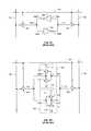
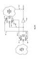
- FIG. 1Ashows an SRAM (Static Random Access Memory) bit cell circuit, in accordance with the prior art.
- the SRAM bit cellincludes two cross-coupled inverters 106 and 102 . Specifically, an output 106 B of inverter 106 is connected to an input 102 A of inverter 102 , and an output 102 B of inverter 102 is connected to an input 106 A of inverter 106 .
- the SRAM bit cellfurther includes two NMOS pass transistors 100 and 104 .
- the NMOS pass transistor 100is connected between a bit-line 103 and a node 109 corresponding to both the output 106 B of inverter 106 and the input 102 A of inverter 102 .
- the NMOS pass transistor 104is connected between a bit-line 105 and a node 111 corresponding to both the output 102 B of inverter 102 and the input 106 A of inverter 106 . Also, the respective gates of NMOS pass transistors 100 and 104 are each connected to a word line 107 , which controls access to the SRAM bit cell through the NMOS pass transistors 100 and 104 .
- the SRAM bit cellrequires bi-directional write, which means that when bit-line 103 is driven high, bit-line 105 is driven low, vice-versa. It should be understood by those skilled in the art that a logic state stored in the SRAM bit cell is maintained in a complementary manner by nodes 109 and 111 .
- FIG. 1Bshows the SRAM bit cell of FIG. 1A with the inverters 106 and 102 expanded to reveal their respective internal transistor configurations, in accordance with the prior art.
- the inverter 106include a PMOS transistor 115 and an NMOS transistor 113 .
- the respective gates of the PMOS and NMOS transistors 115 , 113are connected together to form the input 106 A of inverter 106 .
- each of PMOS and NMOS transistors 115 , 113have one of their respective terminals connected together to form the output 106 B of inverter 106 .
- a remaining terminal of PMOS transistor 115is connected to a power supply 117 .
- a remaining terminal of NMOS transistor 113is connected to a ground potential 119 .
- PMOS and NMOS transistors 115 , 113are activated in a complementary manner.
- the NMOS transistor 113is turned on and the PMOS transistor 115 is turned off, thereby causing a low logic state to be generated at output 106 B of the inverter 106 .
- the NMOS transistor 113is turned off and the PMOS transistor 115 is turned on, thereby causing a high logic state to be generated at output 106 B of the inverter 106 .
- the inverter 102is defined in an identical manner to inverter 106 .
- the inverter 102include a PMOS transistor 121 and an NMOS transistor 123 .
- the respective gates of the PMOS and NMOS transistors 121 , 123are connected together to form the input 102 A of inverter 102 .
- each of PMOS and NMOS transistors 121 , 123have one of their respective terminals connected together to form the output 102 B of inverter 102 .
- a remaining terminal of PMOS transistor 121is connected to the power supply 117 .
- a remaining terminal of NMOS transistor 123is connected to the ground potential 119 . Therefore, PMOS and NMOS transistors 121 , 123 are activated in a complementary manner.
- the NMOS transistor 123When a high logic state is present at the input 102 A of the inverter 102 , the NMOS transistor 123 is turned on and the PMOS transistor 121 is turned off, thereby causing a low logic state to be generated at output 102 B of the inverter 102 .
- the NMOS transistor 123When a low logic state is present at the input 102 A of the inverter 102 , the NMOS transistor 123 is turned off and the PMOS transistor 121 is turned on, thereby causing a high logic state to be generated at output 102 B of the inverter 102 .
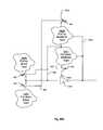
- FIG. 2shows a cross-coupled transistor configuration, in accordance with one embodiment of the present invention.
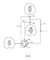
- the cross-coupled transistor configurationincludes four transistors: a PMOS transistor 401 , an NMOS transistor 405 , a PMOS transistor 403 , and an NMOS transistor 407 .
- the PMOS transistor 401has one terminal connected to pull up logic 209 A, and its other terminal connected to a common node 495 .
- the NMOS transistor 405has one terminal connected to pull down logic 211 A, and its other terminal connected to the common node 495 .
- the PMOS transistor 403has one terminal connected to pull up logic 209 B, and its other terminal connected to the common node 495 .
- the NMOS transistor 407has one terminal connected to pull down logic 211 B, and its other terminal connected to the common node 495 . Respective gates of the PMOS transistor 401 and the NMOS transistor 407 are both connected to a gate node 491 . Respective gates of the NMOS transistor 405 and the PMOS transistor 403 are both connected to a gate node 493 .
- the gate nodes 491 and 493are also referred to as control nodes 491 and 493 , respectively.
- each of the common node 495 , the gate node 491 , and the gate node 493can be referred to as an electrical connection 495 , 491 , 493 , respectively.
- the cross-coupled transistor configurationincludes four transistors: 1) a first PMOS transistor, 2) a first NMOS transistor, 3) a second PMOS transistor, and 4) a second NMOS transistor. Furthermore, the cross-coupled transistor configuration includes three required electrical connections: 1) each of the four transistors has one of its terminals connected to a same common node, 2) gates of one PMOS transistor and one NMOS transistor are both connected to a first gate node, and 3) gates of the other PMOS transistor and the other NMOS transistor are both connected to a second gate node.
- the cross-coupled transistor configuration of FIG. 2represents a basic configuration of cross-coupled transistors.
- additional circuitry componentscan be connected to any node within the cross-coupled transistor configuration of FIG. 2 .
- additional circuitry componentscan be inserted between any one or more of the cross-coupled transistors ( 401 , 405 , 403 , 407 ) and the common node 495 , without departing from the cross-coupled transistor configuration of FIG. 2 .
- the SRAM bit cell of FIGS. 1A-1Bdoes not include a cross-coupled transistor configuration.
- the cross-coupled “inverters” 106 and 102 within the SRAM bit cellneither represent nor infer a cross-coupled “transistor” configuration.
- the cross-coupled transistor configurationrequires that each of the four transistors has one of its terminals electrically connected to the same common node. This does not occur in the SRAM bit cell.
- the terminals of PMOS transistor 115 and NMOS transistor 113are connected together at node 109 , but the terminals of PMOS transistor 121 and NMOS transistor 123 are connected together at node 111 . More specifically, the terminals of PMOS transistor 115 and NMOS transistor 113 that are connected together at the output 106 B of the inverter are connected to the gates of each of PMOS transistor 121 and NMOS transistor 123 , and therefore are not connected to both of the terminals of PMOS transistor 121 and NMOS transistor 123 . Therefore, the SRAM bit cell does not include four transistors (two PMOS and two NMOS) that each have one of its terminals connected together at a same common node. Consequently, the SRAM bit cell does represent or include a cross-coupled transistor configuration, such as described with regard to FIG. 2 .
- the present inventionimplements a restricted gate level layout architecture within a portion of a semiconductor chip.
- a number of parallel virtual linesare defined to extend across the layout. These parallel virtual lines are referred to as gate electrode tracks, as they are used to index placement of gate electrodes of various transistors within the layout.
- the parallel virtual lines which form the gate electrode tracksare defined by a perpendicular spacing therebetween equal to a specified gate electrode pitch. Therefore, placement of gate electrode segments on the gate electrode tracks corresponds to the specified gate electrode pitch.
- the gate electrode tracksare spaced at variable pitches greater than or equal to a specified gate electrode pitch.
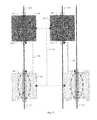
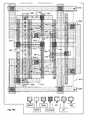
- FIG. 3Ashows an example of gate electrode tracks 301 A- 301 E defined within the restricted gate level layout architecture, in accordance with one embodiment of the present invention.
- Gate electrode tracks 301 A- 301 Eare formed by parallel virtual lines that extend across the gate level layout of the chip, with a perpendicular spacing therebetween equal to a specified gate electrode pitch 307 .
- complementary diffusion regions 303 and 305are shown in FIG. 3A . It should be understood that the diffusion regions 303 and 305 are defined in the diffusion level below the gate level. Also, it should be understood that the diffusion regions 303 and 305 are provided by way of example and in no way represent any limitation on diffusion region size, shape, and/or placement within the diffusion level relative to the restricted gate level layout architecture.
- a gate level feature layout channelis defined about a given gate electrode track so as to extend between gate electrode tracks adjacent to the given gate electrode track.
- gate level feature layout channels 301 A- 1 through 301 E- 1are defined about gate electrode tracks 301 A through 301 E, respectively.
- each gate electrode trackhas a corresponding gate level feature layout channel.
- the corresponding gate level feature layout channelextends as if there were a virtual gate electrode track outside the prescribed layout space, as illustrated by gate level feature layout channels 301 A- 1 and 301 E- 1 .
- each gate level feature layout channelis defined to extend along an entire length of its corresponding gate electrode track.
- each gate level feature layout channelis defined to extend across the gate level layout within the portion of the chip to which the gate level layout is associated.
- gate level features associated with a given gate electrode trackare defined within the gate level feature layout channel associated with the given gate electrode track.
- a contiguous gate level featurecan include both a portion which defines a gate electrode of a transistor, and a portion that does not define a gate electrode of a transistor.
- a contiguous gate level featurecan extend over both a diffusion region and a dielectric region of an underlying chip level.
- each portion of a gate level feature that forms a gate electrode of a transistoris positioned to be substantially centered upon a given gate electrode track.
- portions of the gate level feature that do not form a gate electrode of a transistorcan be positioned within the gate level feature layout channel associated with the given gate electrode track.
- a given gate level featurecan be defined essentially anywhere within a given gate level feature layout channel, so long as gate electrode portions of the given gate level feature are centered upon the gate electrode track corresponding to the given gate level feature layout channel, and so long as the given gate level feature complies with design rule spacing requirements relative to other gate level features in adjacent gate level layout channels. Additionally, physical contact is prohibited between gate level features defined in gate level feature layout channels that are associated with adjacent gate electrode tracks.
- FIG. 3Bshows the exemplary restricted gate level layout architecture of FIG. 3A with a number of exemplary gate level features 309 - 323 defined therein, in accordance with one embodiment of the present invention.
- the gate level feature 309is defined within the gate level feature layout channel 301 A- 1 associated with gate electrode track 301 A.
- the gate electrode portions of gate level feature 309are substantially centered upon the gate electrode track 301 A.
- the non-gate electrode portions of gate level feature 309maintain design rule spacing requirements with gate level features 311 and 313 defined within adjacent gate level feature layout channel 301 B- 1 .
- gate level features 311 - 323are defined within their respective gate level feature layout channel, and have their gate electrode portions substantially centered upon the gate electrode track corresponding to their respective gate level feature layout channel.
- each of gate level features 311 - 323maintains design rule spacing requirements with gate level features defined within adjacent gate level feature layout channels, and avoids physical contact with any another gate level feature defined within adjacent gate level feature layout channels.
- a gate electrodecorresponds to a portion of a respective gate level feature that extends over a diffusion region, wherein the respective gate level feature is defined in its entirety within a gate level feature layout channel.
- Each gate level featureis defined within its gate level feature layout channel without physically contacting another gate level feature defined within an adjoining gate level feature layout channel.
- each gate level feature layout channelis associated with a given gate electrode track and corresponds to a layout region that extends along the given gate electrode track and perpendicularly outward in each opposing direction from the given gate electrode track to a closest of either an adjacent gate electrode track or a virtual gate electrode track outside a layout boundary.
- Some gate level featuresmay have one or more contact head portions defined at any number of locations along their length.
- a contact head portion of a given gate level featureis defined as a segment of the gate level feature having a height and a width of sufficient size to receive a gate contact structure, wherein “width” is defined across the substrate in a direction perpendicular to the gate electrode track of the given gate level feature, and wherein “height” is defined across the substrate in a direction parallel to the gate electrode track of the given gate level feature.
- a contact head of a gate level featurewhen viewed from above, can be defined by essentially any layout shape, including a square or a rectangle. Also, depending on layout requirements and circuit design, a given contact head portion of a gate level feature may or may not have a gate contact defined thereabove.
- a gate level of the various embodiments disclosed hereinis defined as a restricted gate level, as discussed above.
- Some of the gate level featuresform gate electrodes of transistor devices. Others of the gate level features can form conductive segments extending between two points within the gate level. Also, others of the gate level features may be non-functional with respect to integrated circuit operation. It should be understood that the each of the gate level features, regardless of function, is defined to extend across the gate level within their respective gate level feature layout channels without physically contacting other gate level features defined with adjacent gate level feature layout channels.
- the gate level featuresare defined to provide a finite number of controlled layout shape-to-shape lithographic interactions which can be accurately predicted and optimized for in manufacturing and design processes.
- the gate level featuresare defined to avoid layout shape-to-shape spatial relationships which would introduce adverse lithographic interaction within the layout that cannot be accurately predicted and mitigated with high probability.
- changes in direction of gate level features within their gate level layout channelsare acceptable when corresponding lithographic interactions are predictable and manageable.
- each of the gate level featuresregardless of function, is defined such that no gate level feature along a given gate electrode track is configured to connect directly within the gate level to another gate level feature defined along a different gate electrode track without utilizing a non-gate level feature.
- each connection between gate level features that are placed within different gate level layout channels associated with different gate electrode tracksis made through one or more non-gate level features, which may be defined in higher interconnect levels, i.e., through one or more interconnect levels above the gate level, or by way of local interconnect features at or below the gate level.
- the cross-coupled transistor configurationincludes four transistors (2 PMOS transistors and 2 NMOS transistors).
- gate electrodes defined in accordance with the restricted gate level layout architectureare respectively used to form the four transistors of a cross-coupled transistor configuration layout.
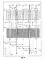
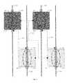
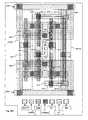
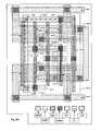
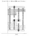
- FIG. 4shows diffusion and gate level layouts of a cross-coupled transistor configuration, in accordance with one embodiment of the present invention.
- the cross-coupled transistor layout of FIG. 4includes the first PMOS transistor 401 defined by a gate electrode 401 A extending along a gate electrode track 450 and over a p-type diffusion region 480 .
- the first NMOS transistor 407is defined by a gate electrode 407 A extending along a gate electrode track 456 and over an n-type diffusion region 486 .
- the second PMOS transistor 403is defined by a gate electrode 403 A extending along the gate electrode track 456 and over a p-type diffusion region 482 .
- the second NMOS transistor 405is defined by a gate electrode 405 A extending along the gate electrode track 450 and over an n-type diffusion region 484 .
- the gate electrodes 401 A and 407 A of the first PMOS transistor 401 and first NMOS transistor 407 , respectively,are electrically connected to the first gate node 491 so as to be exposed to a substantially equivalent gate electrode voltage.
- the gate electrodes 403 A and 405 A of the second PMOS transistor 403 and second NMOS transistor 405are electrically connected to the second gate node 493 so as to be exposed to a substantially equivalent gate electrode voltage.
- each of the four transistors 401 , 403 , 405 , 407has a respective diffusion terminal electrically connected to the common output node 495 .
- the cross-coupled transistor layoutcan be implemented in a number of different ways within the restricted gate level layout architecture.
- the gate electrodes 401 A and 405 A of the first PMOS transistor 401 and second NMOS transistor 405are positioned along the same gate electrode track 450 .
- the gate electrodes 403 A and 407 A of the second PMOS transistor 403 and second NMOS transistor 407are positioned along the same gate electrode track 456 .
- the particular embodiment of FIG. 4can be characterized as a cross-coupled transistor configuration defined on two gate electrode tracks with crossing gate electrode connections.
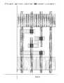
- FIG. 5shows a variation of the cross-coupled transistor configuration of FIG. 4 in which the cross-coupled transistor configuration is defined on three gate electrode tracks with crossing gate electrode connections.
- the gate electrode 401 A of the first PMOS transistor 401is defined on the gate electrode track 450 .
- the gate electrode 403 A of the second PMOS transistor 403is defined on the gate electrode track 456 .
- the gate electrode 407 A of the first NMOS transistor 407is defined on a gate electrode track 456 .
- the gate electrode 405 A of the second NMOS transistor 405is defined on a gate electrode track 448 .
- the particular embodiment of FIG. 5can be characterized as a cross-coupled transistor configuration defined on three gate electrode tracks with crossing gate electrode connections.
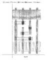
- FIG. 6shows a variation of the cross-coupled transistor configuration of FIG. 4 in which the cross-coupled transistor configuration is defined on four gate electrode tracks with crossing gate electrode connections.
- the gate electrode 401 A of the first PMOS transistor 401is defined on the gate electrode track 450 .
- the gate electrode 403 A of the second PMOS transistor 403is defined on the gate electrode track 456 .
- the gate electrode 407 A of the first NMOS transistor 407is defined on a gate electrode track 458 .
- the gate electrode 405 A of the second NMOS transistor 405is defined on a gate electrode track 454 .
- the particular embodiment of FIG. 6can be characterized as a cross-coupled transistor configuration defined on four gate electrode tracks with crossing gate electrode connections.
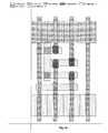
- FIG. 7shows a variation of the cross-coupled transistor configuration of FIG. 4 in which the cross-coupled transistor configuration is defined on two gate electrode tracks without crossing gate electrode connections.
- the gate electrode 401 A of the first PMOS transistor 401is defined on the gate electrode track 450 .
- the gate electrode 407 A of the first NMOS transistor 407is also defined on a gate electrode track 450 .
- the gate electrode 403 A of the second PMOS transistor 403is defined on the gate electrode track 456 .
- the gate electrode 405 A of the second NMOS transistor 405is also defined on a gate electrode track 456 .
- the particular embodiment of FIG. 7can be characterized as a cross-coupled transistor configuration defined on two gate electrode tracks without crossing gate electrode connections.
- FIG. 8shows a variation of the cross-coupled transistor configuration of FIG. 4 in which the cross-coupled transistor configuration is defined on three gate electrode tracks without crossing gate electrode connections.
- the gate electrode 401 A of the first PMOS transistor 401is defined on the gate electrode track 450 .
- the gate electrode 407 A of the first NMOS transistor 407is also defined on a gate electrode track 450 .
- the gate electrode 403 A of the second PMOS transistor 403is defined on the gate electrode track 454 .
- the gate electrode 405 A of the second NMOS transistor 405is defined on a gate electrode track 456 .
- the particular embodiment of FIG. 8can be characterized as a cross-coupled transistor configuration defined on three gate electrode tracks without crossing gate electrode connections.
- FIG. 9shows a variation of the cross-coupled transistor configuration of FIG. 4 in which the cross-coupled transistor configuration is defined on four gate electrode tracks without crossing gate electrode connections.
- the gate electrode 401 A of the first PMOS transistor 401is defined on the gate electrode track 450 .
- the gate electrode 403 A of the second PMOS transistor 403is defined on the gate electrode track 454 .
- the gate electrode 407 A of the first NMOS transistor 407is defined on a gate electrode track 452 .
- the gate electrode 405 A of the second NMOS transistor 405is defined on a gate electrode track 456 .
- the particular embodiment of FIG. 9can be characterized as a cross-coupled transistor configuration defined on four gate electrode tracks without crossing gate electrode connections.
- cross-coupled transistors 401 , 403 , 405 , 407 of FIGS. 4-9are depicted as having their own respective diffusion region 480 , 482 , 484 , 486 , respectively, other embodiments may utilize a contiguous p-type diffusion region for PMOS transistors 401 and 403 , and/or utilize a contiguous n-type diffusion region for NMOS transistors 405 and 407 .
- FIGS. 4-9depict the p-type diffusion regions 480 and 482 in a vertically aligned position, it should be understood that the p-type diffusion regions 480 and 482 may not be vertically aligned in other embodiments.
- FIGS. 4-9depict the n-type diffusion regions 484 and 486 in a vertically aligned position, it should be understood that the n-type diffusion regions 484 and 486 may not be vertically aligned in other embodiments.
- the cross-coupled transistor layout of FIG. 4includes the first PMOS transistor 401 defined by the gate electrode 401 A extending along the gate electrode track 450 and over a first p-type diffusion region 480 .
- the second PMOS transistor 403is defined by the gate electrode 403 A extending along the gate electrode track 456 and over a second p-type diffusion region 482 .
- the first NMOS transistor 407is defined by the gate electrode 407 A extending along the gate electrode track 456 and over a first n-type diffusion region 486 .
- the second NMOS transistor 405is defined by the gate electrode 405 A extending along the gate electrode track 450 and over a second n-type diffusion region 484 .
- the gate electrode tracks 450 and 456extend in a first parallel direction. At least a portion of the first p-type diffusion region 480 and at least a portion of the second p-type diffusion region 482 are formed over a first common line of extent that extends across the substrate perpendicular to the first parallel direction of the gate electrode tracks 450 and 456 . Additionally, at least a portion of the first n-type diffusion region 486 and at least a portion of the second n-type diffusion region 484 are formed over a second common line of extent that extends across the substrate perpendicular to the first parallel direction of the gate electrode tracks 450 and 456 .
- FIG. 14Cshows that two PMOS transistors ( 401 A and 403 A) of the cross-coupled transistors are disposed over a common p-type diffusion region (PDIFF), two NMOS transistors ( 405 A and 407 A) of the cross-coupled transistors are disposed over a common n-type diffusion region (NDIFF), and the p-type (PDIFF) and n-type (NDIFF) diffusion regions associated with the cross-coupled transistors are electrically connected to a common node 495 .
- the gate electrodes of the cross-coupled transistors ( 401 A, 403 A, 405 A, 407 A)extend in a first parallel direction.
- At least a portion of a first p-type diffusion region associated with the first PMOS transistor 401 A and at least a portion of a second p-type diffusion region associated with the second PMOS transistor 403 Aare formed over a first common line of extent that extends across the substrate perpendicular to the first parallel direction of the gate electrodes. Additionally, at least a portion of a first n-type diffusion region associated with the first NMOS transistor 405 A and at least a portion of a second n-type diffusion region associated with the second NMOS transistor 407 A are formed over a second common line of extent that extends across the substrate perpendicular to the first parallel direction of the gate electrodes.
- two PMOS transistors of the cross-coupled transistorsare respectively disposed over physically separated p-type diffusion regions
- two NMOS transistors of the cross-coupled transistorsare disposed over a common n-type diffusion region
- the p-type and n-type diffusion regions associated with the cross-coupled transistorsare electrically connected to a common node.
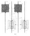
- FIG. 23illustrates a cross-coupled transistor layout embodiment in which two PMOS transistors ( 2301 and 2303 ) of the cross-coupled transistors are respectively disposed over physically separated p-type diffusion regions ( 2302 and 2304 ), two NMOS transistors ( 2305 and 2307 ) of the cross-coupled transistors are disposed over a common n-type diffusion region 2306 , and the p-type ( 2302 , 2304 ) and n-type 2306 diffusion regions associated with the cross-coupled transistors are electrically connected to a common node 2309 .
- FIG. 23shows that the gate electrodes of the cross-coupled transistors ( 2301 , 2303 , 2305 , 2307 ) extend in a first parallel direction 2311 .
- FIG. 23also shows that the first 2302 and second 2304 p-type diffusion regions are formed in a spaced apart manner relative to the first parallel direction 2311 of the gate electrodes, such that no single line of extent that extends across the substrate in a direction 2313 perpendicular to the first parallel direction 2311 of the gate electrodes intersects both the first 2302 and second 2304 p-type diffusion regions. Also, FIG.
- FIG. 23shows that at least a portion of a first n-type diffusion region (part of 2306 ) associated with a first NMOS transistor 2305 and at least a portion of a second n-type diffusion region (part of 2306 ) associated with a second NMOS transistor 2307 are formed over a common line of extent that extends across the substrate in the direction 2313 perpendicular to the first parallel direction 2311 of the gate electrodes.
- two PMOS transistors of the cross-coupled transistorsare disposed over a common p-type diffusion region
- two NMOS transistors of the cross-coupled transistorsare respectively disposed over physically separated n-type diffusion regions
- the p-type and n-type diffusion regions associated with the cross-coupled transistorsare electrically connected to a common node.
- FIG. 24shows the cross-coupled transistor embodiment of FIG. 23 , with the p-type ( 2302 and 2304 ) and n-type 2306 diffusion regions of FIG. 23 reversed to n-type ( 2402 and 2404 ) and p-type 2406 diffusion regions, respectively.
- FIG. 24illustrates a cross-coupled transistor layout embodiment in which two PMOS transistors ( 2405 and 2407 ) of the cross-coupled transistors are disposed over a common p-type diffusion region 2406 , two NMOS transistors ( 2401 and 2403 ) of the cross-coupled transistors are respectively disposed over physically separated n-type diffusion regions ( 2402 and 2404 ), and the p-type 2406 and n-type ( 2402 and 2404 ) diffusion regions associated with the cross-coupled transistors are electrically connected to a common node 2409 . 1471 FIG. 24 shows that the gate electrodes of the cross-coupled transistors ( 2401 , 2403 , 2405 , 2407 ) extend in a first parallel direction 2411 .
- FIG. 24shows that the gate electrodes of the cross-coupled transistors ( 2401 , 2403 , 2405 , 2407 ) extend in a first parallel direction 2411 .
- FIG. 24also shows that at least a portion of a first p-type diffusion region (part of 2406 ) associated with a first PMOS transistor 2405 and at least a portion of a second p-type diffusion region (part of 2406 ) associated with a second PMOS transistor 2407 are formed over a common line of extent that extends across the substrate in a direction 2413 perpendicular to the first parallel direction 2411 of the gate electrodes. Also, FIG.
- first 2402 and second 2404 n-type diffusion regionsare formed in a spaced apart manner relative to the first parallel direction 2411 , such that no single line of extent that extends across the substrate in the direction 2413 perpendicular to the first parallel direction 2411 of the gate electrodes intersects both the first 2402 and second 2404 n-type diffusion regions.
- two PMOS transistors of the cross-coupled transistorsare respectively disposed over physically separated p-type diffusion regions
- two NMOS transistors of the cross-coupled transistorsare respectively disposed over physically separated n-type diffusion regions
- the p-type and n-type diffusion regions associated with the cross-coupled transistorsare electrically connected to a common node.
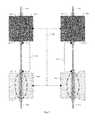
- FIG. 25shows a cross-coupled transistor layout embodiment in which two PMOS transistors ( 2501 and 2503 ) of the cross-coupled transistors are respectively disposed over physically separated p-type diffusion regions ( 2502 and 2504 ), two NMOS transistors ( 2505 and 2507 ) of the cross-coupled transistors are respectively disposed over physically separated n-type diffusion regions ( 2506 and 2508 ), and the p-type ( 2502 and 2504 ) and n-type ( 2506 and 2508 ) diffusion regions associated with the cross-coupled transistors are electrically connected to a common node 2509 .
- FIG. 25shows that the gate electrodes of the cross-coupled transistors ( 2501 , 2503 , 2505 , 2507 ) extend in a first parallel direction 2511 .
- FIG. 25also shows that the first 2502 and second 2504 p-type diffusion regions are formed in a spaced apart manner relative to the first parallel direction 2511 , such that no single line of extent that extends across the substrate in a direction 2513 perpendicular to the first parallel direction 2511 of the gate electrodes intersects both the first 2502 and second 2504 p-type diffusion regions. Also, FIG.
- first 2506 and second 2508 n-type diffusion regionsare formed in a spaced apart manner relative to the first parallel direction 2511 , such that no single line of extent that extends across the substrate in the direction 2513 perpendicular to the first parallel direction 2511 of the gate electrodes intersects both the first 2506 and second 2508 n-type diffusion regions.
- FIGS. 4-9the gate electrode connections are electrically represented by lines 491 and 493 , and the common node electrical connection is represented by line 495 .
- each of the gate electrode electrical connections 491 , 493 , and the common node electrical connection 495can be structurally defined by a number of layout shapes extending through multiple chip levels.
- FIGS. 10-13show examples of how the gate electrode electrical connections 491 , 493 , and the common node electrical connection 495 can be defined in different embodiments. It should be understood that the example layouts of FIGS. 10-13 are provided by way of example and in no way represent an exhaustive set of possible multi-level connections that can be utilized for the gate electrode electrical connections 491 , 493 , and the common node electrical connection 495 .
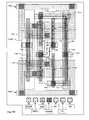
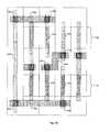
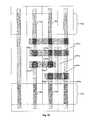
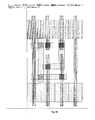
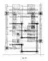
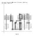
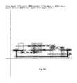
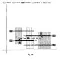
- FIG. 10shows a multi-level layout including a cross-coupled transistor configuration defined on three gate electrode tracks with crossing gate electrode connections, in accordance with one embodiment of the present invention.
- the layout of FIG. 10represents an exemplary implementation of the cross-coupled transistor embodiment of FIG. 5 .
- the electrical connection 491 between the gate electrode 401 A of the first PMOS transistor 401 and the gate electrode 407 A of the first NMOS transistor 407is formed by a multi-level connection that includes a gate contact 1001 , a (two-dimensional) metal-1 structure 1003 , and a gate contact 1005 .
- the electrical connection 493 between the gate electrode 403 A of the second PMOS transistor 403 and the gate electrode 405 A of the second NMOS transistor 405is formed by a multi-level connection that includes a gate contact 1007 , a (two-dimensional) metal-1 structure 1009 , and a gate contact 1011 .
- the output node electrical connection 495is formed by a multi-level connection that includes a diffusion contact 1013 , a (two-dimensional) metal-1 structure 1015 , a diffusion contact 1017 , and a diffusion contact 1019 .
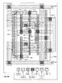
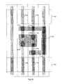
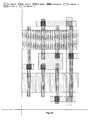
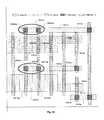
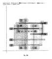
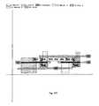
- FIG. 11shows a multi-level layout including a cross-coupled transistor configuration defined on four gate electrode tracks with crossing gate electrode connections, in accordance with one embodiment of the present invention.
- the layout of FIG. 11represents an exemplary implementation of the cross-coupled transistor embodiment of FIG. 6 .
- the electrical connection 491 between the gate electrode 401 A of the first PMOS transistor 401 and the gate electrode 407 A of the first NMOS transistor 407is formed by a multi-level connection that includes a gate contact 1101 , a (two-dimensional) metal-1 structure 1103 , and a gate contact 1105 .
- the electrical connection 493 between the gate electrode 403 A of the second PMOS transistor 403 and the gate electrode 405 A of the second NMOS transistor 405is formed by a multi-level connection that includes a gate contact 1107 , a (one-dimensional) metal-1 structure 1109 , a via 1111 , a (one-dimensional) metal-2 structure 1113 , a via 1115 , a (one-dimensional) metal-1 structure 1117 , and a gate contact 1119 .
- the output node electrical connection 495is formed by a multi-level connection that includes a diffusion contact 1121 , a (two-dimensional) metal-1 structure 1123 , a diffusion contact 1125 , and a diffusion contact 1127 .
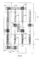
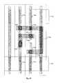
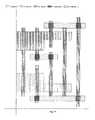
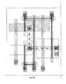
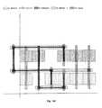
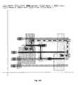
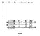
- FIG. 12shows a multi-level layout including a cross-coupled transistor configuration defined on two gate electrode tracks without crossing gate electrode connections, in accordance with one embodiment of the present invention.
- the layout of FIG. 12represents an exemplary implementation of the cross-coupled transistor embodiment of FIG. 7 .
- the gate electrodes 401 A and 407 A of the first PMOS transistor 401 and first NMOS transistor 407are formed by a contiguous gate level structure placed on the gate electrode track 450 . Therefore, the electrical connection 491 between the gate electrodes 401 A and 407 A is made directly within the gate level along the single gate electrode track 450 .
- the gate electrodes 403 A and 405 A of the second PMOS transistor 403 and second NMOS transistor 405are formed by a contiguous gate level structure placed on the gate electrode track 456 . Therefore, the electrical connection 493 between the gate electrodes 403 A and 405 A is made directly within the gate level along the single gate electrode track 456 .
- the output node electrical connection 495is formed by a multi-level connection that includes a diffusion contact 1205 , a (one-dimensional) metal-1 structure 1207 , and a diffusion contact 1209 .
- the corresponding cross-coupled transistor layoutmay include electrical connections between diffusion regions associated with the four cross-coupled transistors 401 , 407 , 403 , 405 , that cross in layout space without electrical communication therebetween.
- diffusion region 1220 of PMOS transistor 403is electrically connected to diffusion region 1222 of NMOS transistor 407 as indicated by electrical connection 1224
- diffusion region 1230 of PMOS transistor 401is electrically connected to diffusion region 1232 of NMOS transistor 405 as indicated by electrical connection 1234 , wherein electrical connections 1224 and 1234 cross in layout space without electrical communication therebetween.
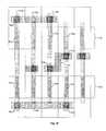
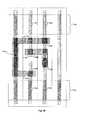
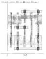
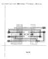
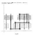
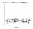
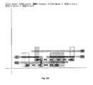
- FIG. 13shows a multi-level layout including a cross-coupled transistor configuration defined on three gate electrode tracks without crossing gate electrode connections, in accordance with one embodiment of the present invention.
- the layout of FIG. 13represents an exemplary implementation of the cross-coupled transistor embodiment of FIG. 8 .
- the gate electrodes 401 A and 407 A of the first PMOS transistor 401 and first NMOS transistor 407are formed by a contiguous gate level structure placed on the gate electrode track 450 . Therefore, the electrical connection 491 between the gate electrodes 401 A and 407 A is made directly within the gate level along the single gate electrode track 450 .
- the electrical connection 493 between the gate electrode 403 A of the second PMOS transistor 403 and the gate electrode 405 A of the second NMOS transistor 405is formed by a multi-level connection that includes a gate contact 1303 , a (one-dimensional) metal-1 structure 1305 , and a gate contact 1307 .
- the output node electrical connection 495is formed by a multi-level connection that includes a diffusion contact 1311 , a (one-dimensional) metal-1 structure 1313 , and a diffusion contact 1315 .
- electrical connection of the diffusion regions of the cross-coupled transistors to the common node 495can be made using one or more local interconnect conductors defined at or below the gate level itself. This embodiment may also combine local interconnect conductors with conductors in higher levels (above the gate level) by way of contacts and/or vias to make the electrical connection of the diffusion regions of the cross-coupled transistors to the common node 495 . Additionally, in various embodiments, conductive paths used to electrically connect the diffusion regions of the cross-coupled transistors to the common node 495 can be defined to traverse over essentially any area of the chip as required to accommodate a routing solution for the chip.
- n-type and p-type diffusion regionsare physically separate, and because the p-type diffusion regions for the two PMOS transistors of the cross-coupled transistors can be physically separate, and because the n-type diffusion regions for the two NMOS transistors of the cross-coupled transistors can be physically separate, it is possible in various embodiments to have each of the four cross-coupled transistors disposed at arbitrary locations in the layout relative to each other. Therefore, unless necessitated by electrical performance or other layout influencing conditions, it is not required that the four cross-coupled transistors be located within a prescribed proximity to each other in the layout. Although, location of the cross-coupled transistors within a prescribed proximity to each other is not precluded, and may be desirable in certain circuit layouts.
- diffusion regionsare not restricted in size.
- any given diffusion regioncan be sized in an arbitrary manner as required to satisfy electrical and/or layout requirements.
- any given diffusion regioncan be shaped in an arbitrary manner as required to satisfy electrical and/or layout requirements.
- the four transistors of the cross-coupled transistor configurationas defined in accordance with the restricted gate level layout architecture, are not required to be the same size.
- the four transistors of the cross-coupled transistor configurationcan either vary in size (transistor width or transistor gate length) or have the same size, depending on the applicable electrical and/or layout requirements.
- the four transistors of the cross-coupled transistor configurationare not required to be placed in close proximity to each, although they may be closely placed in some embodiments. More specifically, because connections between the transistors of the cross-coupled transistor configuration can be made by routing through as least one higher interconnect level, there is freedom in placement of the four transistors of the cross-coupled transistor configuration relative to each other. Although, it should be understood that a proximity of the four transistors of the cross-coupled transistor configuration may be governed in certain embodiments by electrical and/or layout optimization requirements.
- cross-coupled transistor configurations and corresponding layouts implemented using the restricted gate level layout architecturecan be used to form many different electrical circuits.
- a portion of a modern semiconductor chipis likely to include a number of multiplexer circuits and/or latch circuits.
- Such multiplexer and/or latch circuitscan be defined using cross-coupled transistor configurations and corresponding layouts based on the restricted gate level layout architecture, as disclosed herein.
- Example multiplexer embodiments implemented using the restricted gate level layout architecture and corresponding cross-coupled transistor configurationsare described with regard to FIGS. 14A-17C .
- Example latch embodiments implemented using the restricted gate level layout architecture and corresponding cross-coupled transistor configurationsare described with regard to FIGS. 18A-22C . It should be understood that the multiplexer and latch embodiments described with regard to FIGS. 14A-22C are provided by way of example and do not represent an exhaustive set of possible multiplexer and latch embodiments.
- FIG. 14Ashows a generalized multiplexer circuit in which all four cross-coupled transistors 401 , 405 , 403 , 407 are directly connected to the common node 495 , in accordance with one embodiment of the present invention.
- gates of the first PMOS transistor 401 and first NMOS transistor 407are electrically connected, as shown by electrical connection 491 .
- gates of the second PMOS transistor 403 and second NMOS transistor 405are electrically connected, as shown by electrical connection 493 .
- Pull up logic 1401is electrically connected to the first PMOS transistor 401 at a terminal opposite the common node 495 .
- Pull down logic 1403is electrically connected to the second NMOS transistor 405 at a terminal opposite the common node 495 .
- pull up logic 1405is electrically connected to the second PMOS transistor 403 at a terminal opposite the common node 495 .
- Pull down logic 1407is electrically connected to the first NMOS transistor 407 at a terminal opposite the common node 495
- FIG. 14Bshows an exemplary implementation of the multiplexer circuit of FIG. 14A with a detailed view of the pull up logic 1401 and 1405 , and the pull down logic 1403 and 1407 , in accordance with one embodiment of the present invention.
- the pull up logic 1401is defined by a PMOS transistor 1401 A connected between a power supply (VDD) and a terminal 1411 of the first PMOS transistor 401 opposite the common node 495 .
- the pull down logic 1403is defined by an NMOS transistor 1403 A connected between a ground potential (GND) and a terminal 1413 of the second NMOS transistor 405 opposite the common node 495 .
- Respective gates of the PMOS transistor 1401 A and NMOS transistor 1403 Aare connected together at a node 1415 .
- the pull up logic 1405is defined by a PMOS transistor 1405 A connected between the power supply (VDD) and a terminal 1417 of the second PMOS transistor 403 opposite the common node 495 .
- the pull down logic 1407is defined by an NMOS transistor 1407 A connected between a ground potential (GND) and a terminal 1419 of the first NMOS transistor 407 opposite the common node 495 . Respective gates of the PMOS transistor 1405 A and NMOS transistor 1407 A are connected together at a node 1421 . It should be understood that the implementations of pull up logic 1401 , 1405 and pull down logic 1403 , 1407 as shown in FIG. 14B are exemplary. In other embodiments, logic different than that shown in FIG. 14B can be used to implement the pull up logic 1401 , 1405 and the pull down logic 1403 , 1407 .
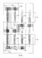
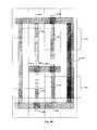
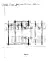
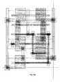
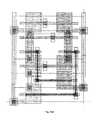
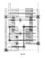
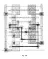
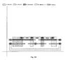
- FIG. 14Cshows a multi-level layout of the multiplexer circuit of FIG. 14B implemented using a restricted gate level layout architecture cross-coupled transistor layout, in accordance with one embodiment of the present invention.
- the electrical connection 491 between the gate electrode 401 A of the first PMOS transistor 401 and the gate electrode 407 A of the first NMOS transistor 407is formed by a multi-level connection that includes a gate contact 1445 , a (two-dimensional) metal-1 structure 1447 , and a gate contact 1449 .
- the electrical connection 493 between the gate electrode 403 A of the second PMOS transistor 403 and the gate electrode 405 A of the second NMOS transistor 405is formed by a multi-level connection that includes a gate contact 1431 , a (one-dimensional) metal-1 structure 1433 , a via 1435 , a (one-dimensional) metal-2 structure 1436 , a via 1437 , a (one-dimensional) metal-1 structure 1439 , and a gate contact 1441 .
- the common node electrical connection 495is formed by a multi-level connection that includes a diffusion contact 1451 , a (one-dimensional) metal-1 structure 1453 , a via 1455 , a (one-dimensional) metal-2 structure 1457 , a via 1459 , a (one-dimensional) metal-1 structure 1461 , and a diffusion contact 1463 .
- Respective gates of the PMOS transistor 1401 A and NMOS transistor 1403 Aare connected to the node 1415 by a gate contact 1443 .
- respective gates of the PMOS transistor 1405 A and NMOS transistor 1407 Aare connected to the node 1421 by a gate contact 1465 .
- FIG. 15Ashows the multiplexer circuit of FIG. 14A in which the two cross-coupled transistors 401 and 405 remain directly connected to the common node 495 , and in which the two cross-coupled transistors 403 and 407 are positioned outside the pull up logic 1405 and pull down logic 1407 , respectively, relative to the common node 495 , in accordance with one embodiment of the present invention.
- Pull up logic 1405is electrically connected between the second PMOS transistor 403 and the common node 495 .
- Pull down logic 1407is electrically connected between the first NMOS transistor 407 and the common node 495 .
- FIG. 15Ais the same as the circuit of FIG. 14A .
- FIG. 15Bshows an exemplary implementation of the multiplexer circuit of FIG. 15A with a detailed view of the pull up logic 1401 and 1405 , and the pull down logic 1403 and 1407 , in accordance with one embodiment of the present invention.
- the pull up logic 1401is defined by the PMOS transistor 1401 A connected between VDD and the terminal 1411 of the first PMOS transistor 401 opposite the common node 495 .
- the pull down logic 1403is defined by NMOS transistor 1403 A connected between GND and the terminal 1413 of the second NMOS transistor 405 opposite the common node 495 .
- Respective gates of the PMOS transistor 1401 A and NMOS transistor 1403 Aare connected together at the node 1415 .
- the pull up logic 1405is defined by the PMOS transistor 1405 A connected between the second PMOS transistor 403 and the common node 495 .
- the pull down logic 1407is defined by the NMOS transistor 1407 A connected between the first NMOS transistor 407 and the common node 495 . Respective gates of the PMOS transistor 1405 A and NMOS transistor 1407 A are connected together at the node 1421 . It should be understood that the implementations of pull up logic 1401 , 1405 and pull down logic 1403 , 1407 as shown in FIG. 15B are exemplary. In other embodiments, logic different than that shown in FIG. 15B can be used to implement the pull up logic 1401 , 1405 and the pull down logic 1403 , 1407 .
- FIG. 15Cshows a multi-level layout of the multiplexer circuit of FIG. 15B implemented using a restricted gate level layout architecture cross-coupled transistor layout, in accordance with one embodiment of the present invention.
- the electrical connection 491 between the gate electrode 401 A of the first PMOS transistor 401 and the gate electrode 407 A of the first NMOS transistor 407is formed by a multi-level connection that includes a gate contact 1501 , a (one-dimensional) metal-1 structure 1503 , a via 1505 , a (one-dimensional) metal-2 structure 1507 , a via 1509 , a (one-dimensional) metal-1 structure 1511 , and a gate contact 1513 .
- the electrical connection 493 between the gate electrode 403 A of the second PMOS transistor 403 and the gate electrode 405 A of the second NMOS transistor 405is formed by a multi-level connection that includes a gate contact 1515 , a (two-dimensional) metal-1 structure 1517 , and a gate contact 1519 .
- the common node electrical connection 495is formed by a multi-level connection that includes a diffusion contact 1521 , a (one-dimensional) metal-1 structure 1523 , a via 1525 , a (one-dimensional) metal-2 structure 1527 , a via 1529 , a (one-dimensional) metal-1 structure 1531 , and a diffusion contact 1533 .
- Respective gates of the PMOS transistor 1401 A and NMOS transistor 1403 Aare connected to the node 1415 by a gate contact 1535 . Also, respective gates of the PMOS transistor 1405 A and NMOS transistor 1407 A are connected to the node 1421 by a gate contact 1539 .
- FIG. 16Ashows a generalized multiplexer circuit in which the cross-coupled transistors ( 401 , 403 , 405 , 407 ) are connected to form two transmission gates 1602 , 1604 to the common node 495 , in accordance with one embodiment of the present invention.
- the cross-coupled transistors401 , 403 , 405 , 407
- gates of the first PMOS transistor 401 and first NMOS transistor 407are electrically connected, as shown by electrical connection 491 .
- gates of the second PMOS transistor 403 and second NMOS transistor 405are electrically connected, as shown by electrical connection 493 .
- the first PMOS transistor 401 and second NMOS transistor 405are connected to form a first transmission gate 1602 to the common node 495 .
- the second PMOS transistor 403 and first NMOS transistor 407are connected to form a second transmission gate 1604 to the common node 495 .
- Driving logic 1601is electrically connected to both the first PMOS transistor 401 and second NMOS transistor 405 at a terminal opposite the common node 495 .
- Driving logic 1603is electrically connected to both the second PMOS transistor 403 and first NMOS transistor 407 at a terminal opposite the common node 495 .
- FIG. 16Bshows an exemplary implementation of the multiplexer circuit of FIG. 16A with a detailed view of the driving logic 1601 and 1603 , in accordance with one embodiment of the present invention.
- the driving logic 1601is defined by an inverter 1601 A and, the driving logic 1603 is defined by an inverter 1603 A.
- the driving logic 1601 and 1603can be defined by any logic function, such as a two input NOR gate, a two input NAND gate, AND-OR logic, OR-AND logic, among others, by way of example.
- FIG. 16Cshows a multi-level layout of the multiplexer circuit of FIG. 16B implemented using a restricted gate level layout architecture cross-coupled transistor layout, in accordance with one embodiment of the present invention.
- the electrical connection 491 between the gate electrode 401 A of the first PMOS transistor 401 and the gate electrode 407 A of the first NMOS transistor 407is formed by a multi-level connection that includes a gate contact 1619 , a (two-dimensional) metal-1 structure 1621 , and a gate contact 1623 .
- the electrical connection 493 between the gate electrode 403 A of the second PMOS transistor 403 and the gate electrode 405 A of the second NMOS transistor 405is formed by a multi-level connection that includes a gate contact 1605 , a (one-dimensional) metal-1 structure 1607 , a via 1609 , a (one-dimensional) metal-2 structure 1611 , a via 1613 , a (one-dimensional) metal-1 structure 1615 , and a gate contact 1617 .
- the common node electrical connection 495is formed by a multi-level connection that includes a diffusion contact 1625 , a (one-dimensional) metal-1 structure 1627 , a via 1629 , a (one-dimensional) metal-2 structure 1631 , a via 1633 , a (one-dimensional) metal-1 structure 1635 , and a diffusion contact 1637 .
- Transistors which form the inverter 1601 Aare shown within the region bounded by the dashed line 1601 AL.
- Transistors which form the inverter 1603 Aare shown within the region bounded by the dashed line 1603 AL.
- FIG. 17Ashows a generalized multiplexer circuit in which two transistors ( 403 , 407 ) of the four cross-coupled transistors are connected to form a transmission gate 1702 to the common node 495 , in accordance with one embodiment of the present invention.
- gates of the first PMOS transistor 401 and first NMOS transistor 407are electrically connected, as shown by electrical connection 491 .
- gates of the second PMOS transistor 403 and second NMOS transistor 405are electrically connected, as shown by electrical connection 493 .
- the second PMOS transistor 403 and first NMOS transistor 407are connected to form the transmission gate 1702 to the common node 495 .
- Driving logic 1701is electrically connected to both the second PMOS transistor 403 and first NMOS transistor 407 at a terminal opposite the common node 495 .
- Pull up driving logic 1703is electrically connected to the first PMOS transistor 401 at a terminal opposite the common node 495 .
- pull down driving logic 1705is electrically connected to the second NMOS transistor 405 at a terminal opposite the common node 495 .
- FIG. 17Bshows an exemplary implementation of the multiplexer circuit of FIG. 17A with a detailed view of the driving logic 1701 , 1703 , and 1705 , in accordance with one embodiment of the present invention.
- the driving logic 1701is defined by an inverter 1701 A.
- the pull up driving logic 1703is defined by a PMOS transistor 1703 A connected between VDD and the first PMOS transistor 401 .
- the pull down driving logic 1705is defined by an NMOS transistor 1705 A connected between GND and the second NMOS transistor 405 . Respective gates of the PMOS transistor 1703 A and NMOS transistor 1705 A are connected together at the node 1707 .
- driving logic 1701 , 1703 , and 1705are exemplary. In other embodiments, logic different than that shown in FIG. 17B can be used to implement the driving logic 1701 , 1703 , and 1705 .
- FIG. 17Cshows a multi-level layout of the multiplexer circuit of FIG. 17B implemented using a restricted gate level layout architecture cross-coupled transistor layout, in accordance with one embodiment of the present invention.
- the electrical connection 491 between the gate electrode 401 A of the first PMOS transistor 401 and the gate electrode 407 A of the first NMOS transistor 407is formed by a multi-level connection that includes a gate contact 1723 , a (two-dimensional) metal-1 structure 1725 , and a gate contact 1727 .
- the electrical connection 493 between the gate electrode 403 A of the second PMOS transistor 403 and the gate electrode 405 A of the second NMOS transistor 405is formed by a multi-level connection that includes a gate contact 1709 , a (one-dimensional) metal-1 structure 1711 , a via 1713 , a (one-dimensional) metal-2 structure 1715 , a via 1717 , a (one-dimensional) metal-1 structure 1719 , and a gate contact 1721 .
- the common node electrical connection 495is formed by a multi-level connection that includes a diffusion contact 1729 , a (one-dimensional) metal-1 structure 1731 , a via 1733 , a (one-dimensional) metal-2 structure 1735 , a via 1737 , a (one-dimensional) metal-1 structure 1739 , and a diffusion contact 1741 .
- Transistors which form the inverter 1701 Aare shown within the region bounded by the dashed line 1701 AL.
- Respective gates of the PMOS transistor 1703 A and NMOS transistor 1705 Aare connected to the node 1707 by a gate contact 1743 .
- FIG. 18Ashows a generalized latch circuit implemented using the cross-coupled transistor configuration, in accordance with one embodiment of the present invention.
- the gates of the first PMOS transistor 401 and first NMOS transistor 407are electrically connected, as shown by electrical connection 491 .
- the gates of the second PMOS transistor 403 and second NMOS transistor 405are electrically connected, as shown by electrical connection 493 .
- Each of the four cross-coupled transistorsare electrically connected to the common node 495 . It should be understood that the common node 495 serves as a storage node in the latch circuit.
- Pull up driver logic 1805is electrically connected to the second PMOS transistor 403 at a terminal opposite the common node 495 .
- Pull down driver logic 1807is electrically connected to the first NMOS transistor 407 at a terminal opposite the common node 495 .
- Pull up feedback logic 1809is electrically connected to the first PMOS transistor 401 at a terminal opposite the common node 495 .
- Pull down feedback logic 1811is electrically connected to the second NMOS transistor 405 at a terminal opposite the common node 495 .
- the common node 495is connected to an input of an inverter 1801 .
- An output of the inverter 1801is electrically connected to a feedback node 1803 . It should be understood that in other embodiments the inverter 1801 can be replaced by any logic function, such as a two input NOR gate, a two input NAND gate, among others, or any complex logic function.
- FIG. 18Bshows an exemplary implementation of the latch circuit of FIG. 18A with a detailed view of the pull up driver logic 1805 , the pull down driver logic 1807 , the pull up feedback logic 1809 , and the pull down feedback logic 1811 , in accordance with one embodiment of the present invention.
- the pull up driver logic 1805is defined by a PMOS transistor 1805 A connected between VDD and the second PMOS transistor 403 opposite the common node 495 .
- the pull down driver logic 1807is defined by an NMOS transistor 1807 A connected between GND and the first NMOS transistor 407 opposite the common node 495 . Respective gates of the PMOS transistor 1805 A and NMOS transistor 1807 A are connected together at a node 1804 .
- the pull up feedback logic 1809is defined by a PMOS transistor 1809 A connected between VDD and the first PMOS transistor 401 opposite the common node 495 .
- the pull down feedback logic 1811is defined by an NMOS transistor 1811 A connected between GND and the second NMOS transistor 405 opposite the common node 495 . Respective gates of the PMOS transistor 1809 A and NMOS transistor 1811 A are connected together at the feedback node 1803 .
- pull up driver logic 1805 , pull down driver logic 1807 , pull up feedback logic 1809 , and pull down feedback logic 1811 as shown in FIG. 18Bare exemplary. In other embodiments, logic different than that shown in FIG. 18B can be used to implement the pull up driver logic 1805 , the pull down driver logic 1807 , the pull up feedback logic 1809 , and the pull down feedback logic 1811 .
- FIG. 18Cshows a multi-level layout of the latch circuit of FIG. 18B implemented using a restricted gate level layout architecture cross-coupled transistor layout, in accordance with one embodiment of the present invention.
- the electrical connection 491 between the gate electrode 401 A of the first PMOS transistor 401 and the gate electrode 407 A of the first NMOS transistor 407is formed by a multi-level connection that includes a gate contact 1813 , a (one-dimensional) metal-1 structure 1815 , a via 1817 , a (one-dimensional) metal-2 structure 1819 , a via 1821 , a (one-dimensional) metal-1 structure 1823 , and a gate contact 1825 .
- the electrical connection 493 between the gate electrode 403 A of the second PMOS transistor 403 and the gate electrode 405 A of the second NMOS transistor 405is formed by a multi-level connection that includes a gate contact 1827 , a (two-dimensional) metal-1 structure 1829 , and a gate contact 1831 .
- the common node electrical connection 495is formed by a multi-level connection that includes a diffusion contact 1833 , a (one-dimensional) metal-1 structure 1835 , a via 1837 , a (one-dimensional) metal-2 structure 1839 , a via 1841 , a (two-dimensional) metal-1 structure 1843 , and a diffusion contact 1845 .
- Transistors which form the inverter 1801are shown within the region bounded by the dashed line 1801 L.
- FIG. 19Ashows the latch circuit of FIG. 18A in which the two cross-coupled transistors 401 and 405 remain directly connected to the output node 495 , and in which the two cross-coupled transistors 403 and 407 are positioned outside the pull up driver logic 1805 and pull down driver logic 1807 , respectively, relative to the common node 495 , in accordance with one embodiment of the present invention.
- Pull up driver logic 1805is electrically connected between the second PMOS transistor 403 and the common node 495 .
- Pull down driver logic 1807is electrically connected between the first NMOS transistor 407 and the common node 495 .
- the circuit of FIG. 19Ais the same as the circuit of FIG. 18A .
- FIG. 19Bshows an exemplary implementation of the latch circuit of FIG. 19A with a detailed view of the pull up driver logic 1805 , pull down driver logic 1807 , pull up feedback logic 1809 , and pull down feedback logic 1811 , in accordance with one embodiment of the present invention.
- the pull up feedback logic 1809is defined by the PMOS transistor 1809 A connected between VDD and the first PMOS transistor 401 opposite the common node 495 .
- the pull down feedback logic 1811is defined by NMOS transistor 1811 A connected between GND and the second NMOS transistor 405 opposite the common node 495 . Respective gates of the PMOS transistor 1809 A and NMOS transistor 1811 A are connected together at the feedback node 1803 .
- the pull up driver logic 1805is defined by the PMOS transistor 1805 A connected between the second PMOS transistor 403 and the common node 495 .
- the pull down driver logic 1807is defined by the NMOS transistor 1807 A connected between the first NMOS transistor 407 and the common node 495 . Respective gates of the PMOS transistor 1805 A and NMOS transistor 1807 A are connected together at the node 1804 .
- pull up driver logic 1805 , pull down driver logic 1807 , pull up feedback logic 1809 , and pull down feedback logic 1811 as shown in FIG. 19Bare exemplary. In other embodiments, logic different than that shown in FIG. 19B can be used to implement the pull up driver logic 1805 , the pull down driver logic 1807 , the pull up feedback logic 1809 , and the pull down feedback logic 1811 .
- FIG. 19Cshows a multi-level layout of the latch circuit of FIG. 19B implemented using a restricted gate level layout architecture cross-coupled transistor layout, in accordance with one embodiment of the present invention.
- the electrical connection 491 between the gate electrode 401 A of the first PMOS transistor 401 and the gate electrode 407 A of the first NMOS transistor 407is formed by a multi-level connection that includes a gate contact 1901 , a (one-dimensional) metal-1 structure 1903 , a via 1905 , a (one-dimensional) metal-2 structure 1907 , a via 1909 , a (one-dimensional) metal-1 structure 1911 , and a gate contact 1913 .
- the electrical connection 493 between the gate electrode 403 A of the second PMOS transistor 403 and the gate electrode 405 A of the second NMOS transistor 405is formed by a multi-level connection that includes a gate contact 1915 , a (two-dimensional) metal-1 structure 1917 , and a gate contact 1919 .
- the common node electrical connection 495is formed by a multi-level connection that includes a diffusion contact 1921 , a (one-dimensional) metal-1 structure 1923 , a via 1925 , a (one-dimensional) metal-2 structure 1927 , a via 1929 , a (two-dimensional) metal-1 structure 1931 , and a diffusion contact 1933 .
- Transistors which form the inverter 1801are shown within the region bounded by the dashed line 1801 L.
- FIG. 20Ashows the latch circuit of FIG. 18A in which the two cross-coupled transistors 403 and 407 remain directly connected to the output node 495 , and in which the two cross-coupled transistors 401 and 405 are positioned outside the pull up feedback logic 1809 and pull down feedback logic 1811 , respectively, relative to the common node 495 , in accordance with one embodiment of the present invention.
- Pull up feedback logic 1809is electrically connected between the first PMOS transistor 401 and the common node 495 .
- Pull down feedback logic 1811is electrically connected between the second NMOS transistor 405 and the common node 495 .
- the circuit of FIG. 20Ais the same as the circuit of FIG. 18A .
- FIG. 20Bshows an exemplary implementation of the latch circuit of FIG. 20A with a detailed view of the pull up driver logic 1805 , pull down driver logic 1807 , pull up feedback logic 1809 , and pull down feedback logic 1811 , in accordance with one embodiment of the present invention.
- the pull up feedback logic 1809is defined by the PMOS transistor 1809 A connected between the first PMOS transistor 401 and the common node 495 .
- the pull down feedback logic 1811is defined by NMOS transistor 1811 A connected between the second NMOS transistor 405 and the common node 495 . Respective gates of the PMOS transistor 1809 A and NMOS transistor 1811 A are connected together at the feedback node 1803 .
- the pull up driver logic 1805is defined by the PMOS transistor 1805 A connected between VDD and the second PMOS transistor 403 .
- the pull down driver logic 1807is defined by the NMOS transistor 1807 A connected between GND and the first NMOS transistor 407 . Respective gates of the PMOS transistor 1805 A and NMOS transistor 1807 A are connected together at the node 1804 .
- pull up driver logic 1805 , pull down driver logic 1807 , pull up feedback logic 1809 , and pull down feedback logic 1811 as shown in FIG. 20Bare exemplary. In other embodiments, logic different than that shown in FIG. 20B can be used to implement the pull up driver logic 1805 , the pull down driver logic 1807 , the pull up feedback logic 1809 , and the pull down feedback logic 1811 .
- FIG. 20Cshows a multi-level layout of the latch circuit of FIG. 20B implemented using a restricted gate level layout architecture cross-coupled transistor layout, in accordance with one embodiment of the present invention.
- the electrical connection 491 between the gate electrode 401 A of the first PMOS transistor 401 and the gate electrode 407 A of the first NMOS transistor 407is formed by a multi-level connection that includes a gate contact 2001 , a (one-dimensional) metal-1 structure 2003 , a via 2005 , a (one-dimensional) metal-2 structure 2007 , a via 2009 , a (one-dimensional) metal-1 structure 2011 , and a gate contact 2013 .
- the electrical connection 493 between the gate electrode 403 A of the second PMOS transistor 403 and the gate electrode 405 A of the second NMOS transistor 405is formed by a multi-level connection that includes a gate contact 2015 , a (one-dimensional) metal-1 structure 2017 , and a gate contact 2019 .
- the common node electrical connection 495is formed by a multi-level connection that includes a diffusion contact 2021 , a (two-dimensional) metal-1 structure 2023 , and a diffusion contact 2025 .
- Transistors which form the inverter 1801are shown within the region bounded by the dashed line 1801 L.
- FIG. 21Ashows a generalized latch circuit in which the cross-coupled transistors ( 401 , 403 , 405 , 407 ) are connected to form two transmission gates 2103 , 2105 to the common node 495 , in accordance with one embodiment of the present invention.
- the cross-coupled transistors401 , 403 , 405 , 407
- gates of the first PMOS transistor 401 and first NMOS transistor 407are electrically connected, as shown by electrical connection 491 .
- gates of the second PMOS transistor 403 and second NMOS transistor 405are electrically connected, as shown by electrical connection 493 .
- the first PMOS transistor 401 and second NMOS transistor 405are connected to form a first transmission gate 2103 to the common node 495 .
- the second PMOS transistor 403 and first NMOS transistor 407are connected to form a second transmission gate 2105 to the common node 495 .
- Feedback logic 2109is electrically connected to both the first PMOS transistor 401 and second NMOS transistor 405 at a terminal opposite the common node 495 .
- Driving logic 2107is electrically connected to both the second PMOS transistor 403 and first NMOS transistor 407 at a terminal opposite the common node 495 .
- the common node 495is connected to the input of the inverter 1801 .
- the output of the inverter 1801is electrically connected to a feedback node 2101 . It should be understood that in other embodiments the inverter 1801 can be replaced by any logic function, such as a two input NOR gate, a two input NAND gate, among others, or any complex logic function.
- FIG. 21Bshows an exemplary implementation of the latch circuit of FIG. 21A with a detailed view of the driving logic 2107 and feedback logic 2109 , in accordance with one embodiment of the present invention.
- the driving logic 2107is defined by an inverter 2107 A.
- the feedback logic 2109is defined by an inverter 2109 A. It should be understood that in other embodiments, the driving logic 2107 and/or 2109 can be defined by logic other than an inverter.
- FIG. 21Cshows a multi-level layout of the latch circuit of FIG. 21B implemented using a restricted gate level layout architecture cross-coupled transistor layout, in accordance with one embodiment of the present invention.
- the electrical connection 491 between the gate electrode 401 A of the first PMOS transistor 401 and the gate electrode 407 A of the first NMOS transistor 407is formed by a multi-level connection that includes a gate contact 2111 , a (one-dimensional) metal-1 structure 2113 , a via 2115 , a (one-dimensional) metal-2 structure 2117 , a via 2119 , a (one-dimensional) metal-1 structure 2121 , and a gate contact 2123 .
- the electrical connection 493 between the gate electrode 403 A of the second PMOS transistor 403 and the gate electrode 405 A of the second NMOS transistor 405is formed by a multi-level connection that includes a gate contact 2125 , a (two-dimensional) metal-1 structure 2127 , and a gate contact 2129 .
- the common node electrical connection 495is formed by a multi-level connection that includes a diffusion contact 2131 , a (one-dimensional) metal-1 structure 2133 , a via 2135 , a (one-dimensional) metal-2 structure 2137 , a via 2139 , a (two-dimensional) metal-1 structure 2141 , and a diffusion contact 2143 .
- Transistors which form the inverter 2107 Aare shown within the region bounded by the dashed line 2107 AL.
- Transistors which form the inverter 2109 Aare shown within the region bounded by the dashed line 2109 AL.
- Transistors which form the inverter 1801are shown within the region bounded by the dashed line 1801 L.
- FIG. 22Ashows a generalized latch circuit in which two transistors ( 403 , 407 ) of the four cross-coupled transistors are connected to form a transmission gate 2105 to the common node 495 , in accordance with one embodiment of the present invention.
- gates of the first PMOS transistor 401 and first NMOS transistor 407are electrically connected, as shown by electrical connection 491 .
- gates of the second PMOS transistor 403 and second NMOS transistor 405are electrically connected, as shown by electrical connection 493 .
- the second PMOS transistor 403 and first NMOS transistor 407are connected to form the transmission gate 2105 to the common node 495 .
- Driving logic 2201is electrically connected to both the second PMOS transistor 403 and first NMOS transistor 407 at a terminal opposite the common node 495 .
- Pull up feedback logic 2203is electrically connected to the first PMOS transistor 401 at a terminal opposite the common node 495 .
- pull down feedback logic 2205is electrically connected to the second NMOS transistor 405 at a terminal opposite the common node 495 .
- FIG. 22Bshows an exemplary implementation of the latch circuit of FIG. 22A with a detailed view of the driving logic 2201 , the pull up feedback logic 2203 , and the pull down feedback logic 2205 , in accordance with one embodiment of the present invention.
- the driving logic 2201is defined by an inverter 2201 A.
- the pull up feedback logic 2203is defined by a PMOS transistor 2203 A connected between VDD and the first PMOS transistor 401 .
- the pull down feedback logic 2205is defined by an NMOS transistor 2205 A connected between GND and the second NMOS transistor 405 . Respective gates of the PMOS transistor 2203 A and NMOS transistor 2205 A are connected together at the feedback node 2101 .
- the driving logic 2201can be defined by logic other than an inverter.
- the pull up feedback logic 2203 and/or pull down feedback logic 2205can be defined logic different than what is shown in FIG. 22B .
- FIG. 22Cshows a multi-level layout of the latch circuit of FIG. 22B implemented using a restricted gate level layout architecture cross-coupled transistor layout, in accordance with one embodiment of the present invention.
- the electrical connection 491 between the gate electrode 401 A of the first PMOS transistor 401 and the gate electrode 407 A of the first NMOS transistor 407is formed by a multi-level connection that includes a gate contact 2207 , a (one-dimensional) metal-1 structure 2209 , a via 2211 , a (one-dimensional) metal-2 structure 2213 , a via 2215 , a (one-dimensional) metal-1 structure 2217 , and a gate contact 2219 .
- the electrical connection 493 between the gate electrode 403 A of the second PMOS transistor 403 and the gate electrode 405 A of the second NMOS transistor 405is formed by a multi-level connection that includes a gate contact 2221 , a (two-dimensional) metal-1 structure 2223 , and a gate contact 2225 .
- the common node electrical connection 495is formed by a multi-level connection that includes a diffusion contact 2227 , a (one-dimensional) metal-1 structure 2229 , a via 2231 , a (one-dimensional) metal-2 structure 2233 , a via 2235 , a (two-dimensional) metal-1 structure 2237 , and a diffusion contact 2239 .
- Transistors which form the inverter 2201 Aare shown within the region bounded by the dashed line 2201 AL.
- Transistors which form the inverter 1801are shown within the region bounded by the dashed line 1801 L.
- a cross-coupled transistor configurationis defined within a semiconductor chip. This embodiment is illustrated in part with regard to FIG. 2 .
- a first P channel transistor ( 401 )is defined to include a first gate electrode ( 401 A) defined in a gate level of the chip.
- a first N channel transistor ( 407 )is defined to include a second gate electrode ( 407 A) defined in the gate level of the chip.
- the second gate electrode ( 407 A) of the first N channel transistor ( 407 )is electrically connected to the first gate electrode ( 401 A) of the first P channel transistor ( 401 ).
- a second P channel transistor ( 403 )is defined to include a third gate electrode ( 403 A) defined in the gate level of a chip.
- a second N channel transistor ( 405 )is defined to include a fourth gate electrode ( 405 A) defined in the gate level of the chip.
- the fourth gate electrode ( 405 A) of the second N channel transistor ( 405 )is electrically connected to the third gate electrode ( 403 A) of the second P channel transistor ( 403 ).
- each of the first P channel transistor ( 401 ), first N channel transistor ( 407 ), second P channel transistor ( 403 ), and second N channel transistor ( 405 )has a respective diffusion terminal electrically connected to a common node ( 495 ).
- one or more of the first P channel transistor ( 401 ), the first N channel transistor ( 407 ), the second P channel transistor ( 403 ), and the second N channel transistor ( 405 )can be respectively implemented by a number of transistors electrically connected in parallel.
- the transistors that are electrically connected in parallelcan be considered as one device corresponding to either of the first P channel transistor ( 401 ), the first N channel transistor ( 407 ), the second P channel transistor ( 403 ), and the second N channel transistor ( 405 ).
- electrical connection of multiple transistors in parallel to form a given transistor of the cross-coupled transistor configurationcan be utilized to achieve a desired drive strength for the given transistor.
- each of the first ( 401 A), second ( 407 A), third ( 403 A), and fourth ( 405 A) gate electrodesis defined to extend along any of a number of gate electrode tracks, such as described with regard to FIG. 3 .
- the number of gate electrode tracksextend across the gate level of the chip in a parallel orientation with respect to each other.
- each of the first ( 401 A), second ( 407 A), third ( 403 A), and fourth ( 405 A) gate electrodescorresponds to a portion of a respective gate level feature defined within a gate level feature layout channel.
- Each gate level featureis defined within its gate level feature layout channel without physically contacting another gate level feature defined within an adjoining gate level feature layout channel.
- Each gate level feature layout channelis associated with a given gate electrode track and corresponds to a layout region that extends along the given gate electrode track and perpendicularly outward in each opposing direction from the given gate electrode track to a closest of either an adjacent gate electrode track or a virtual gate electrode track outside a layout boundary, such as described with regard to FIG. 3B .
- the second gate electrode ( 407 A)is electrically connected to the first gate electrode ( 401 A) through at least one electrical conductor defined within any chip level other than the gate level.
- the fourth gate electrode ( 405 A)is electrically connected to the third gate electrode ( 403 A) through at least one electrical conductor defined within any chip level other than the gate level.
- both the second gate electrode ( 407 A) and the first gate electrode ( 401 A)are formed from a single gate level feature that is defined within a same gate level feature layout channel that extends along a single gate electrode track over both a p type diffusion region and an n type diffusion region.
- the fourth gate electrode ( 405 A)is electrically connected to the third gate electrode ( 403 A) through at least one electrical conductor defined within any chip level other than the gate level.
- both the second gate electrode ( 407 A) and the first gate electrode ( 401 A)are formed from a first gate level feature that is defined within a first gate level feature layout channel that extends along a first gate electrode track over both a p type diffusion region and an n type diffusion region.
- both the fourth gate electrode ( 405 A) and the third gate electrode ( 403 A)are formed from a second gate level feature that is defined within a second gate level feature layout channel that extends along a second gate electrode track over both a p type diffusion region and an n type diffusion region.
- the above-described gate electrode cross-coupled transistor configurationis used to implement a multiplexer having no transmission gates.
- This embodimentis illustrated in part with regard to FIGS. 14-15 .
- a first configuration of pull-up logic ( 1401 )is electrically connected to the first P channel transistor ( 401 ), a first configuration of pull-down logic ( 1407 ) electrically connected to the first N channel transistor ( 407 ), a second configuration of pull-up logic ( 1405 ) electrically connected to the second P channel transistor ( 403 ), and a second configuration of pull-down logic ( 1403 ) electrically connected to the second N channel transistor ( 405 ).
- the first configuration of pull-up logic ( 1401 )is defined by a third P channel transistor ( 1401 A), and the second configuration of pull-down logic ( 1403 ) is defined by a third N channel transistor ( 1403 A). Respective gates of the third P channel transistor ( 1401 A) and third N channel transistor ( 1403 A) are electrically connected together so as to receive a substantially equivalent electrical signal.
- the first configuration of pull-down logic ( 1407 )is defined by a fourth N channel transistor ( 1407 A)
- the second configuration of pull-up logic ( 1405 )is defined by a fourth P channel transistor ( 1405 A). Respective gates of the fourth P channel transistor ( 1405 A) and fourth N channel transistor ( 1407 A) are electrically connected together so as to receive a substantially equivalent electrical signal.
- the above-described gate electrode cross-coupled transistor configurationis used to implement a multiplexer having one transmission gate.
- This embodimentis illustrated in part with regard to FIG. 17 .
- a first configuration of pull-up logic ( 1703 )is electrically connected to the first P channel transistor ( 401 )
- a first configuration of pull-down logic ( 1705 )electrically connected to the second N channel transistor ( 405 )
- mux driving logic ( 1701 )is electrically connected to both the second P channel transistor ( 403 ) and the first N channel transistor ( 407 ).
- the first configuration of pull-up logic ( 1703 )is defined by a third P channel transistor ( 1703 A), and the first configuration of pull-down logic ( 1705 ) is defined by a third N channel transistor ( 1705 A). Respective gates of the third P channel transistor ( 1703 A) and third N channel transistor ( 1705 A) are electrically connected together so as to receive a substantially equivalent electrical signal.
- the mux driving logic ( 1701 )is defined by an inverter ( 1701 A).
- the above-described gate electrode cross-coupled transistor configurationis used to implement a latch having no transmission gates.
- This embodimentis illustrated in part with regard to FIGS. 18-20 .
- pull-up driver logic ( 1805 )is electrically connected to the second P channel transistor ( 403 )
- pull-down driver logic ( 1807 )is electrically connected to the first N channel transistor ( 407 )
- pull-up feedback logic ( 1809 )is electrically connected to the first P channel transistor ( 401 )
- pull-down feedback logic ( 1811 )is electrically connected to the second N channel transistor ( 405 ).
- the latchincludes an inverter ( 1801 ) having an input connected to the common node ( 495 ) and an output connected to a feedback node ( 1803 ).
- Each of the pull-up feedback logic ( 1809 ) and pull-down feedback logic ( 1811 )is connected to the feedback node ( 1803 ).
- the pull-up driver logic ( 1805 )is defined by a third P channel transistor ( 1805 A), and the pull-down driver logic ( 1807 ) is defined by a third N channel transistor ( 1807 A). Respective gates of the third P channel transistor ( 1805 A) and third N channel transistor ( 1807 A) are electrically connected together so as to receive a substantially equivalent electrical signal.
- the pull-up feedback logic ( 1809 )is defined by a fourth P channel transistor ( 1809 A), and the pull-down feedback logic ( 1811 ) is defined by a fourth N channel transistor ( 1811 A). Respective gates of the fourth P channel transistor ( 1809 A) and fourth N channel transistor ( 1811 A) are electrically connected together at the feedback node ( 1803 ).
- the above-described gate electrode cross-coupled transistor configurationis used to implement a latch having two transmission gates.
- driving logic ( 2107 )is electrically connected to both the second P channel transistor ( 403 ) and the first N channel transistor ( 407 ).
- feedback logic ( 2109 )is electrically connected to both the first P channel transistor ( 401 ) and the second N channel transistor ( 405 ).
- the latchfurther includes a first inverter ( 1801 ) having an input connected to the common node ( 495 ) and an output connected to a feedback node ( 2101 ).
- the feedback logic ( 2109 )is electrically connected to the feedback node ( 2101 ).
- the driving logic ( 2107 )is defined by a second inverter ( 2107 A)
- the feedback logic ( 2109 )is defined by a third inverter ( 2109 A).
- the above-described gate electrode cross-coupled transistor configurationis used to implement a latch having one transmission gate.
- driving logic ( 2201 )is electrically connected to both the second P channel transistor ( 403 ) and the first N channel transistor ( 407 ).
- pull up feedback logic ( 2203 )is electrically connected to the first P channel transistor ( 401 ), and pull down feedback logic ( 2205 ) electrically connected to the second N channel transistor ( 405 ).
- the latchfurther includes a first inverter ( 1801 ) having an input connected to the common node ( 495 ) and an output connected to a feedback node ( 2101 ).
- both the pull up feedback logic ( 2203 ) and pull down feedback logic ( 2205 )are electrically connected to the feedback node ( 2101 ).
- the driving logic ( 2201 )is defined by a second inverter ( 2201 A).
- the pull up feedback logic ( 2203 )is defined by a third P channel transistor ( 2203 A) electrically connected between the first P channel transistor ( 401 ) and the feedback node ( 2101 ).
- the pull down feedback logic ( 2205 )is defined by a third N channel transistor ( 2205 A) electrically connected between the second N channel transistor ( 405 ) and the feedback node ( 2101 ).
- cross-coupled transistors devicesare defined and connected to form part of an integrated circuit within a semiconductor chip (“chip” hereafter).
- the chipincludes a number of levels within which different features are defined to form the integrated circuit and cross-coupled transistors therein.
- the chipincludes a substrate within which a number of diffusion regions are formed.
- the chipalso includes a gate level in which a number of gate electrodes are formed.
- the chipfurther includes a number of interconnect levels successively defined above the gate level.
- a dielectric materialis used to electrically separate a given level from its vertically adjacent levels.
- a number of contact featuresare defined to extend vertically through the chip to connect gate electrode features and diffusion regions, respectively, to various interconnect level features.
- a number of via featuresare defined to extend vertically through the chip to connect various interconnect level features.
- the gate level of the various embodiments disclosed hereinis defined as a linear gate level and includes a number of commonly oriented linear gate level features. Some of the linear gate level features form gate electrodes of transistor devices. Others of the linear gate level features can form conductive segments extending between two points within the gate level. Also, others of the linear gate level features may be non-functional with respect to integrated circuit operation. It should be understood that the each of the linear gate level features, regardless of function, is defined to extend across the gate level in a common direction and to be devoid of a substantial change in direction along its length. Therefore, each of the gate level features is defined to be parallel to each other when viewed from a perspective perpendicular to the gate level.
- each of the linear gate electrode featuresregardless of function, is defined such that no linear gate electrode feature along a given line of extent is configured to connect directly within the gate electrode level to another linear gate electrode feature defined along another parallel line of extent, without utilizing a non-gate electrode feature.
- each connection between linear gate electrode features that are placed on different, yet parallel, lines of extentis made through one or more non-gate electrode features, which may be defined in higher interconnect level(s), i.e., through one or more interconnect level(s) above the gate electrode level, or by way of local interconnect features within the linear gate level.
- the linear gate electrode featuresare placed according to a virtual grid or virtual grate. However, it should be understood that in other embodiments the linear gate electrode features, although oriented to have a common direction of extent, are placed without regard to a virtual grid or virtual grate.
- each linear gate electrode featureis defined to be devoid of a substantial change in direction along its line of extent, each linear gate electrode feature may have one or more contact head portion(s) defined at any number of location(s) along its length.
- a contact head portion of a given linear gate electrode featureis defined as a segment of the linear gate electrode feature having a different width than a gate portion of the linear gate electrode feature, i.e., than a portion of the linear gate electrode feature that extends over a diffusion region, wherein “width” is defined across the substrate in a direction perpendicular to the line of extent of the given linear gate electrode feature.
- a contact head of linear gate electrode featurewhen viewed from above, can be defined by essentially any rectangular layout shape, including a square and a rectangle. Also, depending on layout requirements and circuit design, a given contact head portion of a linear gate electrode feature may or may not have a gate contact defined thereabove.
- a substantial change in direction of a linear gate level featureexists when the width of the linear gate level feature at any point thereon changes by more than 50% of the nominal width of the linear gate level feature along its entire length.
- a substantial change in direction of a linear gate level featureexists when the width of the linear gate level feature changes from any first location on the linear gate level feature to any second location on the linear gate level feature by more that 50% of the linear gate level feature width at the first location. Therefore, it should be appreciated that the use of non-linear-shaped gate level features is specifically avoided, wherein a non-linear-shaped gate level feature includes one or more significant bends within a plane of the gate level.
- Each of the linear gate level featureshas a width defined perpendicular to its direction of extent across the gate level.
- the various gate level featurescan be defined to have different widths.
- the various gate level featurescan be defined to have the same width.
- a center-to-center spacing between adjacent linear gate level features, as measured perpendicular to their direction of extent across the gate levelis referred to as gate pitch.
- a uniform gate pitchis used.
- the gate pitchcan vary across the gate level. It should be understood that linear gate level feature width and pitch specifications can be established for a portion of the chip and can be different for separate portions of the chip, wherein the portion of the chip may be of any size and shape.
- Each cross-coupled transistor layout embodimentincludes four cross-coupled transistors, wherein each of these four cross-coupled transistors is defined in part by a respective linear gate electrode feature, and wherein the linear gate electrode features of the cross-coupled transistors are oriented to extend across the layout in a parallel relationship to each other.
- each of the gate electrodes of the four cross-coupled transistorsis associated with, i.e., electrically interfaced with, a respective diffusion region.
- the diffusion regions associated with the gate electrodes of the cross-coupled transistorsare electrically connected to a common node.
- connection of the cross-coupled transistor's diffusion regions to the common nodecan be made in many different ways.
- two PMOS transistors of the cross-coupled transistorsare disposed over a common p-type diffusion region
- two NMOS transistors of the cross-coupled transistorsare disposed over a common n-type diffusion region
- the p-type and n-type diffusion regions associated with the cross-coupled transistorsare electrically connected to a common node.
- 26-99 , 150 - 157 , and 168 - 172illustrate various cross-coupled transistor layout embodiments in which two PMOS transistors of the cross-coupled transistors are disposed over a common p-type diffusion region, two NMOS transistors of the cross-coupled transistors are disposed over a common n-type diffusion region, and the p-type and n-type diffusion regions associated with the cross-coupled transistors are electrically connected to a common node. It should be understood that although FIGS.
- 26-99do not explicitly show an electrical connection of the n-type and p-type diffusion regions of the cross-coupled transistors to a common node, this common node connection between the n-type and p-type diffusion regions of the cross-coupled transistors is present in a full version of the exemplary layouts.
- two PMOS transistors of the cross-coupled transistorsare respectively disposed over physically separated p-type diffusion regions
- two NMOS transistors of the cross-coupled transistorsare disposed over a common n-type diffusion region
- the p-type and n-type diffusion regions associated with the cross-coupled transistorsare electrically connected to a common node.
- 103 , 105 , 112 - 149 , 167 , 184 , and 186illustrate various cross-coupled transistor layout embodiments in which two PMOS transistors of the cross-coupled transistors are respectively disposed over physically separated p-type diffusion regions, two NMOS transistors of the cross-coupled transistors are disposed over a common n-type diffusion region, and the p-type and n-type diffusion regions associated with the cross-coupled transistors are electrically connected to a common node.
- two PMOS transistors of the cross-coupled transistorsare disposed over a common p-type diffusion region
- two NMOS transistors of the cross-coupled transistorsare respectively disposed over physically separated n-type diffusion regions
- the p-type and n-type diffusion regions associated with the cross-coupled transistorsare electrically connected to a common node.
- FIG. 103 , 105 , 112 - 149 , 167 , 184 , and 186 with the p-type and n-type diffusion regions reversed to n-type and p-type, respectively,illustrate various cross-coupled transistor layout embodiments in which two PMOS transistors of the cross-coupled transistors are disposed over a common p-type diffusion region, two NMOS transistors of the cross-coupled transistors are respectively disposed over physically separated n-type diffusion regions, and the p-type and n-type diffusion regions associated with the cross-coupled transistors are electrically connected to a common node.
- two PMOS transistors of the cross-coupled transistorsare respectively disposed over physically separated p-type diffusion regions
- two NMOS transistors of the cross-coupled transistorsare respectively disposed over physically separated n-type diffusion regions
- the p-type and n-type diffusion regions associated with the cross-coupled transistorsare electrically connected to a common node.
- 158 - 166 , 173 - 183 , 185 , and 187 - 191illustrate various cross-coupled transistor layout embodiments in which two PMOS transistors of the cross-coupled transistors are respectively disposed over physically separated p-type diffusion regions, two NMOS transistors of the cross-coupled transistors are respectively disposed over physically separated n-type diffusion regions, and the p-type and n-type diffusion regions associated with the cross-coupled transistors are electrically connected to a common node.
- the electrical connection of the various p-type and n-type diffusion regions associated with the cross-coupled transistors to the common nodecan be made using electrical conductors defined within any level of the chip and within any number of levels of the chip, by way of contact and/or vias, so as to accommodate essentially any cross-coupled layout configuration defined in accordance with the linear gate level restrictions.
- electrical connection of the diffusion regions of the cross-coupled transistors to the common nodecan be made using one or more local interconnect conductors defined within the gate level itself.
- This embodimentmay also combine local interconnect conductors with conductors in higher levels (above the linear gate level) by way of contacts and/or vias to make the electrical connection of the diffusion regions of the cross-coupled transistors to the common node. Additionally, in various embodiments, conductive paths used to electrically connect the diffusion regions of the cross-coupled transistors to the common node can be defined to traverse over essentially any area of the chip as required to accommodate a routing solution for the chip.
- n-type and p-type diffusion regionsare physically separate, and because the p-type diffusion regions for the two PMOS transistors of the cross-coupled transistors can be physically separate, and because the n-type diffusion regions for the two NMOS transistors of the cross-coupled transistors can be physically separate, it is possible in various embodiments to have each of the four cross-coupled transistors disposed at arbitrary locations in the layout relative to each other. Therefore, unless necessitated by electrical performance or other layout influencing conditions, it is not required that the four cross-coupled transistors be located within a prescribed proximity to each other in the layout. Although, location of the cross-coupled transistors within a prescribed proximity to each other is not precluded, and may be desirable in certain circuit layouts.
- FIG. 26is an illustration showing an exemplary cross-coupled transistor layout, in accordance with one embodiment of the present invention.
- the cross-couple layoutincludes four transistors 102 p , 104 p , 106 p , 108 p .
- Transistors 102 p , 106 pare defined over a first diffusion region 110 p .
- Transistors 108 p , 104 pare defined over a second diffusion region 112 p .
- the first diffusion region 110 pis defined such that transistors 102 p and 106 p are NMOS transistors
- the second diffusion region 112 pis defined such that transistors 104 p and 108 p are PMOS transistors.
- the first diffusion region 110 pis defined such that transistors 102 p and 106 p are PMOS transistors
- the second diffusion region 112 pis defined such that transistors 104 p and 108 p are NMOS transistors.
- the separation distance 114 p between the first and second diffusion regions 110 p , 112 pcan vary depending on the requirements of the layout and the area required for connection of the cross-coupled transistors between the first and second diffusion regions 110 p , 112 p.
- diffusion regionsare not restricted in size.
- any given diffusion regioncan be sized in an arbitrary manner as required to satisfy electrical and/or layout requirements.
- any given diffusion regioncan be shaped in an arbitrary manner as required to satisfy electrical and/or layout requirements.
- a cross-coupled transistor configurationcan utilize physically separate n-channel diffusion regions and/or physically separate p-channel diffusion regions. More specifically, the two N-MOS transistors of the cross-coupled transistor configuration can utilize physically separate n-channel diffusion regions, and/or the two P-MOS transistors of the cross-coupled transistor configuration can utilize physically separate p-channel diffusion regions.
- the four transistors of the cross-coupled transistor configurationare not required to be the same size.
- the four transistors of the cross-coupled transistor configurationcan either vary in size (transistor width or transistor gate length) or have the same size, depending on the applicable electrical and/or layout requirements.
- the four transistors of the cross-coupled transistor configurationare not required to be placed in close proximity to each, although they may be closely placed in some embodiments. More specifically, because connections between the transistors of the cross-coupled transistor configuration can be made by routing through as least one higher interconnect level, there is freedom in placement of the four transistors of the cross-coupled transistor configuration relative to each other. Although, it should be understood that a proximity of the four transistors of the cross-coupled transistor configuration may be governed in certain embodiments by electrical and/or layout optimization requirements.
- each of linear gate level features 116 Ap- 116 Fpis defined to extend across the gate level in a common direction and to be devoid of a substantial change in direction along its length.
- Linear gate level features 116 Bp, 116 Fp, 116 Cp, and 116 Epform the gate electrodes of transistors 102 p , 104 p , 106 p , and 108 p , respectively.
- the gate electrodes of transistors 106 p and 108 pare connected through gate contacts 118 p and 120 p , and through a higher interconnect level feature 101 p .
- the interconnect level feature 101 pis a first interconnect level feature, i.e., Metal-1 level feature.
- the interconnect level feature 101 pcan be a higher interconnect level feature, such as a Metal-2 level feature, or Metal-3 level feature.
- edges of the interconnect level feature 101 pare substantially aligned with edges of neighboring interconnect level features 103 p , 105 p .
- other embodimentsmay have interconnect level features placed without regard to interconnect level feature alignment or an interconnect level grid.
- the gate contacts 118 p and 120 pare substantially aligned with neighboring contact features 122 p and 124 p , respectively, such that the gate contacts are placed according to a gate contact grid.
- other embodimentsmay have gate contacts placed without regard to gate contact alignment or gate contact grid.
- the gate electrode of transistor 102 pis connected to the gate electrode of transistor 104 p through gate contact 126 p , through interconnect level (e.g., Metal-1 level) feature 130 p , through via 132 p , through higher interconnect level (e.g., Metal-2 level) feature 134 p , through via 136 p , through interconnect level (e.g., Metal-1 level) feature 138 p , and through gate contacts 128 p .
- interconnect levele.g., Metal-1 level
- 26utilizes the Metal-1 and Metal-2 levels to connect the gate electrodes of transistors 102 p and 104 p it should be appreciated that in various embodiment, essentially any combination of interconnect levels can be used to make the connection between the gate electrodes of transistors 102 p and 104 p.
- the cross-coupled transistor layout of FIG. 26is defined using four transistors ( 102 p , 104 p , 106 p , 108 p ) and four gate contacts ( 126 p , 128 p , 118 p , 120 p ).
- the layout embodiment of FIG. 26can be characterized in that two of the four gate contacts are placed between the NMOS and PMOS transistors of the cross-coupled transistors, one of the four gate contacts is placed outside of the NMOS transistors, and one of the four gate contacts is placed outside of the PMOS transistors.
- the two gate contacts placed between the NMOS and PMOS transistorsare referred to as “inner gate contacts.”
- the two gate contacts placed outside of the NMOS and PMOS transistorsare referred to as “outer gate contacts.”
- the direction in which the linear gate level features extend across the layoutis referred to as a “vertical direction.”
- the direction that is perpendicular to the direction in which the linear gate level features extend across the layoutis referred to as a “horizontal direction.”
- the horizontal and vertical interconnect level features 130 p , 134 p , 138 p used to connect the outer gate contacts 126 p , 128 pcan be placed essentially anywhere in the layout, i.e., can be horizontally shifted in either direction away from the cross-coupled transistors 102 p , 104 p , 106 p , 108 p , as necessary to satisfy particular layout/routing requirements.
- FIG. 27is an illustration showing the exemplary layout of FIG. 26 , with the linear gate electrode features 116 Bp, 116 Cp, 116 Ep, and 116 Fp defined to include contact head portions 117 Bp, 117 Cp, 117 Ep, and 117 Fp, respectively.
- a linear gate electrode featureis allowed to have one or more contact head portion(s) along its line of extent, so long as the linear gate electrode feature does not connect directly within the gate level to another linear gate electrode feature having a different, yet parallel, line of extent.
- FIG. 28is an illustration showing the cross-coupled transistor layout of FIG. 26 , with the horizontal positions of the inner gate contacts 118 p , 120 p and outer gate contacts 126 p , 128 p respectively reversed, in accordance with one embodiment of the present invention. It should be understood that essentially any cross-coupled transistor configuration layout defined in accordance with a linear gate level can be represented in an alternate manner by horizontally and/or vertically reversing placement of the gate contacts that are used to connect one or both pairs of the four transistors of the cross-coupled transistor configuration.
- any cross-coupled transistor configuration layout defined in accordance with a linear gate levelcan be represented in an alternate manner by maintaining gate contact placements and by modifying each routing path used to connect one or both pairs of the four transistors of the cross-coupled transistor configuration.
- FIG. 29is an illustration showing the cross-coupled transistor layout of FIG. 26 , with the vertical positions of the inner gate contacts 118 p and 120 p adjusted to enable alignment of the line end spacings between co-linearly aligned gate level features, in accordance with one embodiment of the present invention. Specifically, gate contact 118 p is adjusted vertically upward, and gate contact 120 p is adjusted vertically downward. The linear gate level features 116 Bp and 116 Ep are then adjusted such that the line end spacing 142 p therebetween is substantially vertically centered within area shadowed by the interconnect level feature 101 p .
- linear gate level features 116 Cp and 116 Fpare then adjusted such that the line end spacing 140 p therebetween is substantially vertically centered within area shadowed by the interconnect level feature 101 p . Therefore, the line end spacing 142 p is substantially vertically aligned with the line end spacing 140 p . This vertical alignment of the line end spacings 142 p and 140 p allows for use of a cut mask to define the line end spacings 142 p and 140 p .
- linear gate level features 116 Bp and 116 Epare initially defined as a single continuous linear gate level feature
- linear gate level features 116 Cp and 116 Fpare initially defined as a single continuous linear gate level feature.
- a cut maskis used to remove a portion of each of the single continuous linear gate level features so as to form the line end spacings 142 p and 140 p .
- the layout of FIG. 29may also be fabricated without using a cut mask.
- each embodiment disclosed herein as being suitable for fabrication through use of a cut maskmay also be fabricated without using a cut mask.
- the gate contacts 118 p and 120 pare adjusted vertically so as to be edge-aligned with the interconnect level feature 101 p .
- edge alignment between gate contact and interconnect level featureis not required in all embodiments.
- the gate contacts 118 p and 120 pmay not be edge-aligned with the interconnect level feature 101 p , although they could be if so desired.
- FIG. 30is an illustration showing the cross-coupled transistor layout of FIG. 29 , with the horizontal positions of the inner gate contacts 118 p , 120 p and outer gate contacts 126 p , 128 p respectively reversed, in accordance with one embodiment of the present invention.
- FIG. 31is an illustration showing the cross-coupled transistor layout of FIG. 26 , with the rectangular-shaped interconnect level feature 101 p replaced by an S-shaped interconnect level feature 144 p , in accordance with one embodiment of the present invention.
- the S-shaped interconnect level feature 144 pcan be defined as a first interconnect level feature, i.e., as a Metal-1 level feature.
- the S-shaped interconnect level feature 144 pmay be defined within an interconnect level other than the Metal-1 level.
- FIG. 32is an illustration showing the cross-coupled transistor layout of FIG. 31 , with the horizontal positions of the inner gate contacts 118 p , 120 p and outer gate contacts 126 p , 128 p respectively reversed, in accordance with one embodiment of the present invention. It should be appreciated that the S-shaped interconnect level feature 144 p is flipped horizontally relative to the embodiment of FIG. 31 to enable connection of the inner contacts 120 p and 118 p.
- FIG. 33is an illustration showing the cross-coupled transistor layout of FIG. 31 , with a linear gate level feature 146 p used to make the vertical portion of the connection between the outer contacts 126 p and 128 p , in accordance with one embodiment of the present invention.
- the embodiment of FIG. 31uses vias 132 p and 136 p , and the higher level interconnect feature 134 p to make the vertical portion of the connection between the outer contacts 126 p and 128 p
- the embodiment of FIG. 33uses gate contacts 148 p and 150 p
- the linear gate level feature 146 pto make the vertical portion of the connection between the outer contacts 126 p and 128 p .
- FIG. 33uses gate contacts 148 p and 150 p , and the linear gate level feature 146 p to make the vertical portion of the connection between the outer contacts 126 p and 128 p .
- the linear gate level feature 146 pserves as a conductor, and is not used to define a gate electrode of a transistor. It should be understood that the linear gate level feature 146 p , used to connect the outer gate contacts 126 p and 128 p , can be placed essentially anywhere in the layout, i.e., can be horizontally shifted in either direction away from the cross-coupled transistors 102 p , 104 p , 106 p , 108 p , as necessary to satisfy particular layout requirements.
- FIG. 34is an illustration showing the cross-coupled transistor layout of FIG. 33 , with the horizontal positions of the inner gate contacts 118 p , 120 p and outer gate contacts 126 p , 128 p respectively reversed, in accordance with one embodiment of the present invention.
- FIG. 35is an illustration showing the cross-coupled transistor layout of FIG. 33 defined in connection with a multiplexer (MUX), in accordance with one embodiment of the present invention.
- MUXmultiplexer
- the embodiment of FIG. 35utilizes a select inverter of the MUX to make the vertical portion of the connection between the outer contacts 126 p and 128 p , wherein the select inverter of the MUX is defined by transistors 152 p and 154 p .
- transistor 102 p of the cross-coupled transistorsis driven through transistor 152 p of the select inverter.
- transistor 104 p of the cross-coupled transistorsis driven through transistor 154 p of the select inverter.
- the linear gate level feature 116 Gpused to define the transistors 152 p and 154 p of the select inverter and used to connect the outer gate contacts 126 p and 128 p , can be placed essentially anywhere in the layout, i.e., can be horizontally shifted in either direction away from the cross-coupled transistors 102 p , 104 p , 106 p , 108 p , as necessary to satisfy particular layout requirements.
- FIG. 36is an illustration showing the cross-coupled transistor layout of FIG. 35 , with the horizontal positions of the inner gate contacts 118 p , 120 p and outer gate contacts 126 p , 128 p respectively reversed, in accordance with one embodiment of the present invention.
- FIG. 37is an illustration showing a latch-type cross-coupled transistor layout, in accordance with one embodiment of the present invention.
- the latch-type cross-coupled transistor layout of FIG. 37is similar to that of FIG. 33 , with the exception that the gate widths of transistors 102 p and 108 p are reduced relative to the gate widths of transistors 106 p and 104 p . Because transistors 102 p and 108 p perform a signal keeping function as opposed to a signal driving function, the gate widths of transistors 102 p and 108 p can be reduced. As with the embodiment of FIG.
- the outer gate contact 126 pis connected to the outer gate contact 128 p by way of the interconnect level feature 130 p , the gate contact 148 p , the linear gate level feature 146 p , the gate contact 150 p , and the interconnect level feature 138 p.
- the inner gate contacts 120 p and 118 pcan be vertically aligned. Vertical alignment of the inner gate contacts 120 p and 118 p may facilitate contact fabrication, e.g., contact lithographic resolution. Also, vertical alignment of the inner gate contacts 120 p and 118 p allows for use of simple linear-shaped interconnect level feature 156 p to connect the inner gate contacts 120 p and 118 p .
- vertical alignment of the inner gate contacts 120 p and 118 pallows for increased vertical separation of the line end spacings 142 p and 140 p , which may facilitate creation of the line end spacings 142 p and 140 p when formed using separate cut shapes in a cut mask.
- FIG. 38is an illustration showing the cross-coupled transistor layout of FIG. 37 , with the horizontal positions of the inner gate contacts 120 p , 118 p and outer gate contacts 126 p , 128 p respectively reversed, in accordance with one embodiment of the present invention.
- FIG. 39is an illustration showing the cross-coupled transistor layout of FIG. 37 , with the interconnect level feature 134 p used to make the vertical portion of the connection between the outer contacts 126 p and 128 p , in accordance with one embodiment of the present invention.
- the embodiment of FIG. 37uses gate contacts 148 p and 150 p , and the linear gate level feature 146 p to make the vertical portion of the connection between the outer contacts 126 p and 128 p
- the embodiment of FIG. 39uses vias 132 p and 136 p , and the interconnect level feature 134 p to make the vertical portion of the connection between the outer contacts 126 p and 128 p .
- FIG. 39uses vias 132 p and 136 p , and the interconnect level feature 134 p to make the vertical portion of the connection between the outer contacts 126 p and 128 p .
- the interconnect level feature 134 pis defined as second interconnect level feature, i.e., Metal-2 level feature. However, in other embodiments, the interconnect level feature 134 p can be defined within an interconnect level other than the second interconnect level. It should be understood that the interconnect level feature 134 p , used to connect the outer gate contacts 126 p and 128 p , can be placed essentially anywhere in the layout, i.e., can be horizontally shifted in either direction away from the cross-coupled transistors 102 p , 104 p , 106 p , 108 p , as necessary to satisfy layout requirements.
- FIG. 40is an illustration showing the cross-coupled transistor layout of FIG. 39 , with the horizontal positions of the inner gate contacts 120 p , 118 p and outer gate contacts 126 p , 128 p respectively reversed, in accordance with one embodiment of the present invention.
- FIG. 41is an illustration showing the latch-type cross-coupled transistor layout of FIG. 37 , defined in connection with a MUX/latch, in accordance with one embodiment of the present invention.
- the embodiment of FIG. 41utilizes a select/clock inverter of the MUX/latch to make the vertical portion of the connection between the outer contacts 126 p and 128 p , wherein the select/clock inverter of the MUX/latch is defined by transistors 160 p and 162 p .
- transistor 102 p of the cross-coupled transistorsis driven through transistor 160 p of the select/clock inverter.
- transistor 104 p of the cross-coupled transistorsis driven through transistor 162 p of the select/clock inverter.
- the linear gate level feature 164 pused to define the transistors 160 p and 162 p of the select/clock inverter and used to connect the outer gate contacts 126 p and 128 p , can be placed essentially anywhere in the layout, i.e., can be horizontally shifted in either direction away from the cross-coupled transistors 102 p , 104 p , 106 p , 108 p , as necessary to satisfy particular layout requirements.
- FIG. 42is an illustration showing the cross-coupled transistor layout of FIG. 41 , with the horizontal positions of the inner gate contacts 118 p , 120 p and outer gate contacts 126 p , 128 p respectively reversed, in accordance with one embodiment of the present invention.
- FIG. 43is an illustration showing the latch-type cross-coupled transistor layout of FIG. 37 , defined to have the outer gate contacts 126 p and 128 p connected using a single interconnect level, in accordance with one embodiment of the present invention.
- the embodiment of FIG. 43uses a single interconnect level to make the horizontal and vertical portions of the connection between the outer contacts 126 p and 128 p .
- the gate electrode of transistor 102 pis connected to the gate electrode of transistor 104 p through gate contact 126 p , through horizontal interconnect level feature 166 p , through vertical interconnect level feature 168 p , through horizontal interconnect level feature 170 p , and through gate contact 128 p .
- the interconnect level features 166 p , 168 p , and 170 pare first interconnect level features (Metal-1 features).
- the interconnect level features 166 p , 168 p , and 170 pcan be defined collectively within any other interconnect level.
- FIG. 44is an illustration showing the cross-coupled transistor layout of FIG. 43 , with the horizontal positions of the inner gate contacts 118 p , 120 p and outer gate contacts 126 p , 128 p respectively reversed, in accordance with one embodiment of the present invention.
- FIG. 45is an illustration showing a cross-coupled transistor layout in which all four gate contacts 126 p , 128 p , 118 p , and 120 p of the cross-coupled coupled transistors are placed therebetween, in accordance with one embodiment of the present invention. Specifically, the gate contacts 126 p , 128 p , 118 p , and 120 p of the cross-coupled coupled transistors are placed vertically between the diffusion regions 110 p and 112 p that define the cross-coupled coupled transistors.
- the gate electrode of transistor 102 pis connected to the gate electrode of transistor 104 p through gate contact 126 p , through horizontal interconnect level feature 172 p , through vertical interconnect level feature 174 p , through horizontal interconnect level feature 176 p , and through gate contact 128 p .
- the interconnect level features 172 p , 174 p , and 176 pare first interconnect level features (Metal-1 features).
- the interconnect level features 172 p , 174 p , and 176 pcan be defined collectively within any other interconnect level.
- the gate electrode of transistor 108 pis connected to the gate electrode of transistor 106 p through gate contact 120 p , through S-shaped interconnect level feature 144 p , and through gate contact 118 p .
- the S-shaped interconnect level feature 144 pcan be defined within any interconnect level. In one embodiment, the S-shaped interconnect level feature is defined within the first interconnect level (Metal-1 level).
- FIG. 46is an illustration showing the cross-coupled transistor layout of FIG. 45 , with multiple interconnect levels used to connect the gate contacts 126 p and 128 p , in accordance with one embodiment of the present invention.
- the gate electrode of transistor 102 pis connected to the gate electrode of transistor 104 p through gate contact 126 p , through horizontal interconnect level feature 172 p , through via 180 p , through vertical interconnect level feature 178 p , through via 182 p , through horizontal interconnect level feature 176 p , and through gate contact 128 p .
- the horizontal interconnect level features 172 p and 176 pare defined within the same interconnect level, e.g., Metal-1 level, and the vertical interconnect level feature 178 p is defined within a higher interconnect level, e.g., Metal-2 level. It should be understood, however, that in other embodiments each of interconnect level features 172 p , 178 p , and 176 p can be defined in separate interconnect levels.
- FIG. 47is an illustration showing the cross-coupled transistor layout of FIG. 45 , with increased vertical separation between line end spacings 184 p and 186 p , in accordance with one embodiment of the present invention.
- the increased vertical separation between line end spacings 184 p and 186 pcan facilitate creation of the line end spacings 184 p and 186 p when formed using separate cut shapes in a cut mask.
- FIG. 48is an illustration showing the cross-coupled transistor layout of FIG. 45 , using an L-shaped interconnect level feature 188 p to connect the gate contacts 120 p and 118 p , in accordance with one embodiment of the present invention.
- FIG. 49is an illustration showing the cross-coupled transistor layout of FIG. 48 , with the horizontal position of gate contacts 126 p and 118 p reversed, and with the horizontal position of gate contacts 120 p and 128 p reversed, in accordance with one embodiment of the present invention.
- FIG. 50is an illustration showing the cross-coupled transistor layout of FIG. 48 , with increased vertical separation between line end spacings 184 p and 186 p , in accordance with one embodiment of the present invention.
- the increased vertical separation between line end spacings 184 p and 186 pcan facilitate creation of the line end spacings 184 p and 186 p when formed using separate cut shapes in a cut mask.
- FIG. 51is an illustration showing the cross-coupled transistor layout of FIG. 45 , in which gate contacts 120 p and 118 p are vertically aligned, in accordance with one embodiment of the present invention.
- a linear-shaped interconnect level feature 190 pis used to connect the vertically aligned gate contacts 120 p and 118 p .
- an increased vertical separation between line end spacings 184 p and 186 pis provided to facilitate creation of the line end spacings 184 p and 186 p when formed using separate cut shapes in a cut mask, although use of a cut mask to fabricate the layout of FIG. 51 is not specifically required.
- FIG. 52is an illustration showing the cross-coupled transistor layout of FIG. 45 , in which a linear-shaped interconnect level feature 192 p is used to connect the non-vertically-aligned gate contacts 120 p and 118 p , in accordance with one embodiment of the present invention. It should be appreciated that the linear-shaped interconnect level feature 192 p is stretched vertically to cover both of the gate contacts 120 p and 118 p.
- FIG. 53is an illustration showing the cross-coupled transistor layout of FIG. 52 , with multiple interconnect levels used to connect the gate contacts 126 p and 128 p , in accordance with one embodiment of the present invention.
- the gate electrode of transistor 102 pis connected to the gate electrode of transistor 104 p through gate contact 126 p , through horizontal interconnect level feature 172 p , through via 180 p , through vertical interconnect level feature 178 p , through via 182 p , through horizontal interconnect level feature 176 p , and through gate contact 128 p .
- the horizontal interconnect level features 172 p and 176 pare defined within the same interconnect level, e.g., Metal-1 level, and the vertical interconnect level feature 178 p is defined within a higher interconnect level, e.g., Metal-2 level. It should be understood, however, that in other embodiments each of interconnect level features 172 p , 178 p , and 176 p can be defined in separate interconnect levels.
- FIG. 54is an illustration showing the cross-coupled transistor layout of FIG. 53 , with the vertical positions of gate contacts 118 p and 120 p adjusted to enable alignment of the line end spacings between co-linearly aligned gate level features, in accordance with one embodiment of the present invention. Specifically, gate contact 118 p is adjusted vertically upward, and gate contact 120 p is adjusted vertically downward. The linear gate level features 116 Bp and 116 Ep are then adjusted such that the line end spacing 184 p therebetween is substantially vertically centered within area shadowed by the interconnect level feature 192 p .
- linear gate level features 116 Cp and 116 Fpare then adjusted such that the line end spacing 186 p therebetween is substantially vertically centered within area shadowed by the interconnect level feature 192 p . Therefore, the line end spacing 184 p is substantially vertically aligned with the line end spacing 186 p . This vertical alignment of the line end spacings 184 p and 186 p allows for use of a cut mask to define the line end spacings 184 p and 186 p .
- linear gate level features 116 Bp and 116 Epare initially defined as a single continuous linear gate level feature
- linear gate level features 116 Cp and 116 Fpare initially defined as a single continuous linear gate level feature.
- a cut maskis used to remove a portion of each of the single continuous linear gate level features so as to form the line end spacings 184 p and 186 p .
- edge-alignment between the gate contacts 118 p , 120 p and the interconnect level feature 192 pcan be utilized in one embodiment, it should be understood that such edge-alignment between gate contact and interconnect level feature is not required in all embodiments.
- FIG. 55is an illustration showing a cross-coupled transistor layout in which the four gate contacts 126 p , 128 p , 120 p , and 118 p are placed within three consecutive horizontal tracks of an interconnect level, in accordance with one embodiment of the present invention.
- the gate electrode of transistor 102 pis connected to the gate electrode of transistor 104 p through gate contact 126 p , through horizontal interconnect level feature 402 p , through gate contact 418 p , through vertical gate level feature 404 p , through gate contact 416 p , through horizontal interconnect level feature 424 . p , and through gate contact 128 p .
- the vertical gate level feature 404 prepresents a common node to which the gate electrodes of transistors 426 p and 428 p are connected. It should be understood that the vertical gate level feature 404 p can be shifted left or right relative to the cross-coupled transistors 102 p , 104 p , 106 p , 108 p , as necessary for layout purposes. Also, the gate electrode of transistor 106 p is connected to the gate electrode of transistor 108 p through gate contact 118 p , through horizontal interconnect level feature 190 p , and through gate contact 120 p.
- interconnect level features 402 p , 424 p , and 190 pcan be defined in the same interconnect level or in different interconnect levels. In one embodiment, each of the interconnect level features 402 p , 424 p , and 190 p is defined in a first interconnect level (Metal-1 level).
- FIG. 56is an illustration showing the cross-coupled transistor layout of FIG. 55 , in which a non-transistor gate level feature 430 p is used to make the vertical portion of the connection between gate contacts 126 p and 126 p , in accordance with one embodiment of the present invention.
- the gate electrode of transistor 102 pis connected to the gate electrode of transistor 104 p through gate contact 126 p , through horizontal interconnected level feature 402 p , through gate contact 418 p , through vertical non-transistor gate level feature 430 p , through gate contact 416 p , through horizontal interconnect level feature 424 p , and through gate contact 128 p.
- FIG. 57is an illustration showing a cross-coupled transistor layout in which the four gate contacts 126 p , 128 p , 120 p , and 118 p are placed within three consecutive horizontal tracks of an interconnect level, and in which multiple interconnect levels are used to connect the gate contacts 126 p and 128 p , in accordance with one embodiment of the present invention.
- the gate electrode of transistor 102 pis connected to the gate electrode of transistor 104 p through gate contact 126 p , through horizontal interconnect level feature 432 p , through via 434 p , through vertical interconnect level feature 436 p , through via 438 p , through horizontal interconnect level feature 440 p , and through gate contact 128 p .
- the vertical interconnect level feature 436 pis defined within an interconnect level different from the interconnect level in which the horizontal interconnect level features 432 p and 440 p are defined.
- the horizontal interconnect level features 432 p and 440 pare defined within a first interconnect level (Metal-1 level)
- the vertical interconnect level feature 436 pis defined within a second interconnect level (Metal-2 level).
- the vertical interconnect level feature 436 pcan be shifted left or right relative to the cross-coupled transistors 102 p , 104 p , 106 p , 108 p , as necessary for layout purposes.
- the gate electrode of transistor 106 pis connected to the gate electrode of transistor 108 p through gate contact 118 p , through horizontal interconnect level feature 190 p , and through gate contact 120 p.
- FIG. 58is an illustration showing the cross-coupled transistor layout of FIG. 57 , in which the gate contacts 126 Ap, 118 Ap, 120 Ap, and 128 Ap are extended in the vertical direction to provided additional overlap with their respective underlying gate level feature, in accordance with one embodiment of the present invention.
- the additional overlap of the gate level features by the gate contacts 126 Ap, 118 Ap, 120 Ap, and 128 Apmay be provided to satisfy design rules.
- FIG. 59is an illustration showing the cross-coupled transistor layout of FIG. 57 , in which the gate contacts 126 p , 118 p , 120 p , and 128 p are placed within four consecutive interconnect level tracks with an intervening vacant interconnect level track 704 p , in accordance with one embodiment of the present invention.
- the gate electrode of transistor 102 pis connected to the gate electrode of transistor 104 p through gate contact 126 p , through horizontal interconnect level feature 432 p , through via 434 p , through vertical interconnect level feature 436 p , through via 438 p , through horizontal interconnect level feature 440 p , and through gate contact 128 p .
- the gate electrode of transistor 106 pis connected to the gate electrode of transistor 108 p through gate contact 118 p , through L-shaped interconnect level feature 450 p , and through gate contact 120 p .
- the L-shaped interconnect level feature 450 pcan be extended beyond the gate contacts 120 p and 118 p to provide sufficient overlap of the gate contacts by the L-shaped interconnect level feature 450 p , as needed to satisfy design rules.
- FIG. 60is an illustration showing the cross-coupled transistor layout of FIG. 59 , with a variation in the overlap of the gate contact 120 p by the L-shaped interconnect level feature 450 p , in accordance with one embodiment of the present invention.
- the overlap region 709 pis turned horizontally so as to align with the horizontal interconnect level feature 440 p.
- FIGS. 61-94are illustrations showing variants of the cross-coupled transistor layouts of FIGS. 26 and 28 - 60 , respectively.
- essentially any cross-coupled transistor layout defined in accordance with a linear gate levelcan be represented in an alternate manner by horizontally and/or vertically reversing placement of the gate contacts that are used to connect one or both pairs of the four transistors of the cross-coupled transistor configuration.
- essentially any cross-coupled transistor layout defined in accordance with a linear gate levelcan be represented in an alternate manner by maintaining gate contact placements and by modifying each routing path used to connect one or both pairs of the four transistors of the cross-coupled transistor configuration.
- FIGS. 95-99show exemplary cross-coupled transistor layouts defined in accordance with the linear gate level, in which a folded transistor layout technique is implemented.
- a folded transistoris defined as a plurality of transistors whose gate electrodes share an identical electrical connectivity configuration.
- each individual transistor of a given folded transistorhas its gate electrode connected to a common node and is defined to electrically interface with a common diffusion region.
- the common diffusion regionit is not required that the common diffusion region be continuous, i.e., monolithic.
- diffusion regions that are of the same type but are physically separated from each other, and have an electrical connection to a common output node, and share a common source/drainsatisfy the common diffusion region characteristic of the folded transistor.
- a first pair of the cross-coupled transistorsis defined by a folded transistor 6901 Ap/ 6901 Bp and by a transistor 6903 p .
- Each of the individual transistors 6901 Ap and 6901 Bp that form the folded transistoris connected to a common diffusion region 6905 p and has its gate electrode connected to a common node 6907 p through respective gate contacts 6909 Ap and 6909 Bp.
- the gate contacts 6909 Ap and 6909 Bpare connected to a gate contact 6921 p of transistor 6903 p by way of a metal 1 interconnect level feature 6911 p , a contact 6913 p , a gate level feature 6915 p , a contact 6917 p , and a metal 1 interconnect level feature 6919 p .
- a second pair of the cross-coupled transistorsis defined by a folded transistor 6923 Ap/ 6923 Bp and by a transistor 6925 p .
- Each of the individual transistors 6923 Ap and 6923 Bp that form the folded transistoris connected to a common diffusion region 6927 p and has its gate electrode connected to a common node 6929 p through respective gate contacts 6931 Ap and 6931 Bp.
- the gate contacts 693 lAp and 6931 Bpare connected to a gate contact 6933 p of transistor 6925 p by way of a metal 1 interconnect level feature 6935 p .
- Transistors 6901 Ap, 6901 Bp, and 6925 pare electrically interfaced with the diffusion region 6905 p .
- transistors 6923 Ap, 6923 Bp, and 6903 pare electrically interfaced with the diffusion region 6927 p .
- diffusion regions 6905 p and 6927 pare connected to a common output node.
- FIG. 96shows a variant of the cross-coupled transistor layout of FIG. 95 , in which the connection between the folded transistor 6901 Ap/ 6901 Bp and the transistor 6903 p is made using an alternate conductive path through the chip.
- the gate contacts 6909 Ap and 6909 Bpare connected to the gate contact 6921 p of transistor 6903 p by way of a metal 1 interconnect level feature 7001 p , a via 7003 p , a metal 2 interconnect level feature 7005 p , a via 7007 p , and a metal 1 interconnect level feature 7009 p.
- a first pair of the cross-coupled transistorsis defined by a folded transistor 7101 Ap/ 7101 Bp and by a folded transistor 7103 Ap/ 7103 Bp.
- Gate contacts 7105 Ap and 7105 Bpare connected to gate contacts 7107 Ap and 7107 Bp by way of a metal 1 interconnect level feature 7109 p , a via 7111 p , a metal 2 interconnect level feature 7113 p , a via 7115 p , and a metal 1 interconnect level feature 7117 p .
- a second pair of the cross-coupled transistorsis defined by a folded transistor 7119 Ap/ 7119 Bp and by a folded transistor 7121 Ap/ 7121 Bp.
- Gate contacts 7123 Ap and 7123 Bpare connected to gate contacts 7125 Ap and 7125 Bp by way of a metal 1 interconnect level feature 7127 p , a via 7129 p , a metal 2 interconnect level feature 7131 p , a via 7133 p , a metal 1 interconnect level feature 7135 p , a via 7137 p , a metal 2 interconnect level feature 7139 p , a via 7141 p , and a metal 1 interconnect level feature 7143 p .
- Transistors 7101 Ap, 7101 Bp, 7121 Ap, and 7121 Bpare electrically interfaced with diffusion region 7145 p .
- transistors 7119 Ap, 7119 Bp, 7103 Ap, and 7103 Bpare electrically interfaced with diffusion region 7147 p . Additionally, although not explicitly shown, portions of diffusion regions 7145 p and 7147 p which are electrically interfaced with the transistors 7101 Ap, 7101 Bp, 7103 Ap, 7103 Bp, 7119 Ap, 7119 Bp, 7121 Ap, and 7121 Bp are connected to a common output node.
- FIG. 98shows a variant of the cross-coupled transistor layout of FIG. 97 , in which the electrical connections between the cross-coupled transistors are made using an alternate conductive paths through the chip.
- the gate contacts 7105 Ap and 7105 Bpare connected to the gate contacts 7107 Ap and 7107 Bp by way of a metal 1 interconnect level feature 7201 p , a contact 7203 p , a gate level feature 7205 p , a contact 7207 p , and a metal 1 interconnect level feature 7209 p .
- the gate contacts 7123 Ap and 7123 Bpare connected to the gate contacts 7125 Ap and 7125 Bp by way of a metal 1 interconnect level feature 7211 p .
- the metal 1 interconnect levelin unrestricted with regard to bends in conductive features. Therefore, the metal 1 interconnect level feature 7211 p can be defined to “snake” through the metal 1 interconnect level to make the required cross-coupled transistor connections, as permitted by surrounding layout features.
- FIG. 99shows a variant of the cross-coupled transistor layout of FIG. 97 , in which the connection between the folded transistor 7101 Ap/ 7101 Bp and the folded transistor 7103 Ap/ 7103 Bp is made using an alternate conductive path through the chip.
- the gate contacts 7105 Ap and 7105 Bpare connected to the gate contacts 7107 Ap and 7107 Bp by way of the metal 1 interconnect level feature 7201 p , the contact 7203 p , the gate level feature 7205 p , the contact 7207 p , and the metal 1 interconnect level feature 7209 p .
- the cross-coupled transistor layouts utilizing folded transistors as shown in FIGS. 95-99are provided by way of example, and should not be construed as fully inclusive.
- the cross-coupled transistor connectionshave been described by tracing through the various conductive features of each conductive path used to connect each pair of transistors in the cross-coupled layout. It should be appreciated that the conductive path used to connect each pair of transistors in a given cross-coupled layout can traverse through conductive features any number of levels of the chip, utilizing any number of contacts and vias as necessary. For ease of description with regard to FIGS. 100 through 192 , the conductive paths used to connect the various NMOS/PMOS transistor pairs in each cross-coupled transistor layout are identified by heavy black lines drawn over the corresponding layout features.
- FIGS. 26-99do not explicitly show connection of the diffusion regions of the cross-coupled transistors to a common node, although this connection is present.
- FIGS. 100-111show exemplary cross-coupled transistor layouts in which the n-type and p-type diffusion regions of the cross-coupled transistors are shown to be electrically connected to a common node.
- the conductive path used to connect the diffusion regions of the cross-coupled transistors to the common node in each of FIGS. 100-111is identified by a heavy black dashed line drawn over the corresponding layout features.
- FIGS. 112-148do not show the heavy black dashed line corresponding to the conductive path used to connect the diffusion regions of the cross-coupled transistors to the common node.
- FIGS. 112-148do show the layout features associated with the conductive path, or a portion thereof, used to connect the diffusion regions of the cross-coupled transistors to the common node.
- each of the exemplary cross-coupled transistor layoutincludes a conductive path that connects the diffusion regions of the cross-coupled transistors to a common output node.
- FIGS. 112-148show a number of exemplary cross-coupled transistor layouts in which the p-type diffusion regions that are electrically interfaced with the cross-coupled transistors are physically separated from each other.
- the p-type diffusion region 8601 pis physically separated from the p-type diffusion region 8603 p .
- the p-type diffusion regions 8601 p and 8603 pare electrically connected to each other by way of contact 8605 p , metal 1 interconnect level feature 8607 p , and contact 8609 p .
- the diffusion regions 8601 p and 8603 pare also electrically connected to diffusion region 8611 p .
- each cross-coupled transistor layout as shown in each of FIGS. 112-148can be defined by changing the p-type diffusion regions as shown to n-type diffusion regions, and by also changing the n-type diffusion regions as shown to p-type diffusions regions. Therefore, such variants of FIGS. 112-148 illustrate a number of exemplary cross-coupled transistor layouts in which the n-type diffusion regions that are electrically interfaced with the cross-coupled transistors are physically separated from each other.
- FIGS. 149-175show a number of exemplary cross-coupled transistor layouts defined using two gate contacts to connect one pair of complementary (i.e., NMOS/PMOS) transistors in the cross-coupled transistor layout to each other, and using no gate contact to connect the other pair of complementary transistors in the cross-coupled transistor layout to each other.
- two gate electrodes of each pair of cross-coupled transistorswhen considered as a single node, are electrically connected through at least one gate contact to circuitry external to the cross-coupled transistor portion of the layout. Therefore, it should be understood that the gate electrodes mentioned above, or absence thereof, with regard to connecting each pair of complementary transistors in the cross-coupled transistor layout, refer to gate electrodes defined within the cross-coupled transistor portion of the layout.
- FIG. 149shows a cross-coupled transistor layout in which a gate electrode of transistor 12301 p is electrically connected to a gate electrode of transistor 12303 p by way of two gate contacts 12309 p and 12311 p in combination with other conductive features.
- the gate electrodes of transistors 12305 p and 12307 pare defined as a single, continuous linear conductive feature within the gate level. Therefore, a gate contact is not required to electrically connect the gate electrodes of transistors 12305 p and 12307 p .
- the conductive path used to connect the diffusion regions of the cross-coupled transistors to the common output node in each of FIGS. 149-175is identified by a heavy black dashed line drawn over the corresponding layout features.
- the cross-coupled transistor layout defined using two gate contacts to connect one pair of complementary transistors and no gate contact to connect the other pair of complementary transistorscan be implemented in as few as two gate electrode tracks, wherein a gate electrode track is defined as a virtual line extending across the gate level in a parallel relationship to its neighboring gate electrode tracks. These two gate electrode tracks can be located essentially anywhere in the layout with regard to each other. In other words, these two gate electrode tracks are not required to be located adjacent to each other, although such an arrangement is permitted, and in some embodiments may be desirable.
- the cross-coupled transistor layout embodiments of FIGS. 149-175can be characterized in that two gate electrodes of one pair of connected complementary transistors in the cross-coupled layout are defined from a single, continuous linear conductive feature defined in the gate level.
- FIGS. 176-191show a number of exemplary cross-coupled transistor layouts defined using no gate contacts to connect each pair of complementary transistors in the cross-coupled transistor layout.
- two gate electrodes of each pair of cross-coupled transistorswhen considered as a single node, are electrically connected through at least one gate contact to circuitry external to the cross-coupled transistor portion of the layout. Therefore, it should be understood that the absence of gate electrodes with regard to connecting each pair of complementary transistors in the cross-coupled transistor layout refers to an absence of gate electrodes defined within the cross-coupled transistor portion of the layout.
- FIG. 176shows a cross-coupled transistor layout in which gate electrodes of transistors 15001 p and 15003 p are defined as a single, continuous linear conductive feature within the gate level. Therefore, a gate contact is not required to electrically connect the gate electrodes of transistors 15001 p and 15003 p .
- gate electrodes of transistors 15005 p and 15007 pare defined as a single, continuous linear conductive feature within the gate level. Therefore, a gate contact is not required to electrically connect the gate electrodes of transistors 15005 p and 15007 p .
- each pair of connected complementary transistors in the cross-coupled layouthas its gate electrodes defined from a single, continuous linear conductive feature defined in the gate level.
- FIG. 192shows another exemplary cross-couple transistor layout in which the common diffusion node shared between the cross-coupled transistors 16601 p , 16603 p , 16605 p , and 16607 p has one or more transistors defined thereover.
- FIG. 192shows that transistors 16609 Ap and 16609 Bp are defined over the diffusion region 16613 p between transistors 16605 p and 16603 p .
- FIG. 192shows that transistors 16611 Ap and 16611 Bp are defined over the diffusion region 16615 p between transistors 16601 p and 16607 p .
- diffusion regions 16613 p and 16615 pdefine the common diffusion node to which each of the cross-coupled transistors 16601 p , 16603 p , 16605 p , and 16607 p is electrically interfaced.
- driver transistorssuch as transistors 16609 Ap, 16609 Bp, 16611 Ap, and 16611 Bp, can be disposed over the common diffusion node of the cross-coupled transistors.
- the cross-coupled transistorscan be considered as being placed “outside” of the driver transistors.
- the cross-coupled transistor layout using a linear gate levelcan be defined in a number of different ways.
- a number of observations associated with the cross-coupled transistor layout defined using the linear gate levelare as follows:
- FIGS. 26-192a number of features and connections are not shown in order to avoid unnecessarily obscuring the cross-couple transistors in the various layouts.
- connections to source and drainsare not shown.
- some features and connections that are not directly associated with the four cross-coupled transistorsare displayed for exemplary purposes and are not intended to represent any restriction on the correspondingly displayed cross-coupled transistor layout.
- a cross-coupled transistor layout using commonly oriented linear gate level features and transistors having physically separate gate electrodescan be defined according to either of the following embodiments, among others:
- the cross-coupled transistor layouts implemented within the restricted gate level layout architecture as disclosed hereincan be stored in a tangible form, such as in a digital format on a computer readable medium.
- the invention described hereincan be embodied as computer readable code on a computer readable medium.
- the computer readable mediumis any data storage device that can store data which can thereafter be read by a computer system. Examples of the computer readable medium include hard drives, network attached storage (NAS), read-only memory, random-access memory, CD-ROMs, CD-Rs, CD-RWs, magnetic tapes, and other optical and non-optical data storage devices.
- the computer readable mediumcan also be distributed over a network of coupled computer systems so that the computer readable code is stored and executed in a distributed fashion.
- the inventionalso relates to a device or an apparatus for performing these operations.
- the apparatusmay be specially constructed for the required purpose, such as a special purpose computer.
- the computercan also perform other processing, program execution or routines that are not part of the special purpose, while still being capable of operating for the special purpose.
- the operationsmay be processed by a general purpose computer selectively activated or configured by one or more computer programs stored in the computer memory, cache, or obtained over a network. When data is obtained over a network the data maybe processed by other computers on the network, e.g., a cloud of computing resources.
- the embodiments of the present inventioncan also be defined as a machine that transforms data from one state to another state.
- the datamay represent an article, that can be represented as an electronic signal and electronically manipulate data.
- the transformed datacan, in some cases, be visually depicted on a display, representing the physical object that results from the transformation of data.
- the transformed datacan be saved to storage generally, or in particular formats that enable the construction or depiction of a physical and tangible object.
- the manipulationcan be performed by a processor.
- the processorthus transforms the data from one thing to another.
- the methodscan be processed by one or more machines or processors that can be connected over a network. Each machine can transform data from one state or thing to another, and can also process data, save data to storage, transmit data over a network, display the result, or communicate the result to another machine.
Landscapes
- Engineering & Computer Science (AREA)
- Physics & Mathematics (AREA)
- Computer Hardware Design (AREA)
- Theoretical Computer Science (AREA)
- Geometry (AREA)
- General Physics & Mathematics (AREA)
- General Engineering & Computer Science (AREA)
- Evolutionary Computation (AREA)
- Microelectronics & Electronic Packaging (AREA)
- Condensed Matter Physics & Semiconductors (AREA)
- Power Engineering (AREA)
- Architecture (AREA)
- Design And Manufacture Of Integrated Circuits (AREA)
- Metal-Oxide And Bipolar Metal-Oxide Semiconductor Integrated Circuits (AREA)
- Semiconductor Memories (AREA)
- Semiconductor Integrated Circuits (AREA)
Abstract
Description
| Application Ser. No. | |||
| 12/753,711 | Apr. 2, 2010 | ||
| 12/753,727 | Apr. 2, 2010 | ||
| 12/753,733 | Apr. 2, 2010 | ||
| 12/753,740 | Apr. 2, 2010 | ||
| 12/753,753 | Apr. 2, 2010 | ||
| 12/753,758 | Apr. 2, 2010 | ||
| 12/753,766 | Apr. 2, 2010 | ||
| 12/753,776 | Apr. 2, 2010 | ||
| 12/753,789 | Apr. 2, 2010 | ||
| 12/753,793 | Apr. 2, 2010 | ||
| 12/753,795 | Apr. 2, 2010 | ||
| 12/753,798 | Apr. 2, 2010 | ||
| 12/753,805 | Apr. 2, 2010 | ||
| 12/753,810 | Apr. 2, 2010 | ||
| 12/753,817 | Apr. 2, 2010 | ||
| 12/754,050 | Apr. 5, 2010 | ||
| 12/754,061 | Apr. 5, 2010 | ||
| 12/754,078 | Apr. 5, 2010 | ||
| 12/754,091 | Apr. 5, 2010 | ||
| 12/754,103 | Apr. 5, 2010 | ||
| 12/754,129 | Apr. 5, 2010 | ||
| 12/754,147 | Apr. 5, 2010 | ||
| 12/754,168 | Apr. 5, 2010 | ||
| 12/754,215 | Apr. 5, 2010 | ||
| 12/754,233 | Apr. 5, 2010 | ||
| 12/754,351 | Apr. 5, 2010 | ||
| 12/754,384 | Apr. 5, 2010 | ||
| 12/754,563 | Apr. 5, 2010 | ||
| 12/754,566 | Apr. 5, 2010 | ||
- In one embodiment, an interconnect level parallel to the gate level is used to connect the two “outside” transistors, i.e., to connect the two outer gate contacts.
- In one embodiment, the end gaps, i.e., line end spacings, between co-aligned gate electrode features in the area between the n and p diffusion regions can be substantially vertically aligned to enable line end cutting.
- In one embodiment, the end gaps, i.e., line end spacings, between gate electrode features in the area between the n and p diffusion regions can be separated as much as possible to allow for separation of cut shapes, or to prevent alignment of gate electrode feature line ends.
- In one embodiment, the interconnect levels can be configured so that contacts can be placed on a grid to enhance contact printing.
- In one embodiment, the contacts can be placed so that a minimal number of first interconnect level (Metal-1 level) tracks are occupied by the cross-couple connection.
- In one embodiment, the contacts can be placed to maximize the available diffusion area for device size, e.g., transistor width.
- In one embodiment, the contacts can be shifted toward the edges of the interconnect level features to which they connect to allow for better alignment of gate electrode feature line ends.
- In pertinent embodiments, it should be noted that the vertical connection between the outside transistors of the cross-coupled transistor layout can be shifted left or right depending on the specific layout requirements.
- There is no distance requirement between the n and p diffusion regions. If there are more interconnect level tracks available between the n and p diffusion region, the available interconnect level tracks can be allocated as necessary/appropriate for the layout.
- The four transistors of the cross-coupled transistor configuration, as defined in accordance with the linear gate level, can be separated from each other within the layout by arbitrary distances in various embodiments.
- In one embodiment, the linear gate electrode features are placed according to a virtual grid or virtual grate. However, it should be understood that in other embodiments the linear gate electrode features, although oriented to have a common direction of extent, are placed without regard to a virtual grid or virtual grate.
- Each linear gate electrode feature is allowed to have one or more contact head portion(s) along its line of extent, so long as the linear gate electrode feature does not connect directly within the gate level to another linear gate electrode feature having a different, yet parallel, line of extent.
- Diffusion regions associated with the cross-coupled transistor configuration, as defined in accordance with the linear gate level, are not restricted in size or shape.
- The four transistors of the cross-coupled transistor configuration, as defined in accordance with the linear gate level, may vary in size as required to satisfy electrical requirements.
- Essentially any cross-coupled transistor configuration layout defined in accordance with a linear gate level can be represented in an alternate manner by horizontally and/or vertically reversing placement of the gate contacts that are used to connect one or both pairs of the four transistors of the cross-coupled transistor configuration.
- Essentially any cross-coupled transistor configuration layout defined in accordance with a linear gate level can be represented in an alternate manner by maintaining gate contact placements and by modifying each routing path used to connect one or both pairs of the four transistors of the cross-coupled transistor configuration.
- A cross-coupled transistor configuration layout defined in accordance with a linear gate level can be optimized for a fabrication process that utilizes a cut mask.
- In various embodiments, connections between gates of cross-coupled transistors can be made in essentially any manner by utilizing any level within the chip, any number of levels in the chip, any number of contacts, and/or any number of vias.
- all four gate contacts used to connect each pair of complementary transistors in the cross-coupled transistor layout are placed between the diffusion regions associated with the cross-coupled transistor layout,
- two gate contacts used to connect one pair of complementary transistors placed between the diffusion regions associated with the cross-coupled transistor layout, and two gate contacts used to connect another pair of complementary transistors placed outside the diffusion regions with one of these two gate contacts placed outside of each diffusion region,
- all four gate contacts used to connect each pair of complementary transistors placed outside the diffusion regions associated with the cross-coupled transistor layout,
- three gate contacts placed outside the diffusion regions associated with the cross-coupled transistor layout, and one gate contact placed between the diffusion regions associated with the cross-coupled transistor layout, and
- three gate contacts placed between the diffusion regions associated with the cross-coupled transistor layout, and one gate contact placed outside one of the diffusion regions associated with the cross-coupled transistor layout.
Claims (24)
Priority Applications (1)
| Application Number | Priority Date | Filing Date | Title |
|---|---|---|---|
| US12/754,114US8558322B2 (en) | 2008-03-13 | 2010-04-05 | Integrated circuit including cross-coupled transistors having gate electrodes formed within gate level feature layout channels with at least two gate electrodes electrically connected to each other through gate level feature |
Applications Claiming Priority (6)
| Application Number | Priority Date | Filing Date | Title |
|---|---|---|---|
| US3646008P | 2008-03-13 | 2008-03-13 | |
| US4270908P | 2008-04-04 | 2008-04-04 | |
| US4595308P | 2008-04-17 | 2008-04-17 | |
| US5013608P | 2008-05-02 | 2008-05-02 | |
| US12/402,465US7956421B2 (en) | 2008-03-13 | 2009-03-11 | Cross-coupled transistor layouts in restricted gate level layout architecture |
| US12/754,114US8558322B2 (en) | 2008-03-13 | 2010-04-05 | Integrated circuit including cross-coupled transistors having gate electrodes formed within gate level feature layout channels with at least two gate electrodes electrically connected to each other through gate level feature |
Related Parent Applications (1)
| Application Number | Title | Priority Date | Filing Date |
|---|---|---|---|
| US12/402,465ContinuationUS7956421B2 (en) | 2006-03-09 | 2009-03-11 | Cross-coupled transistor layouts in restricted gate level layout architecture |
Publications (2)
| Publication Number | Publication Date |
|---|---|
| US20100237429A1 US20100237429A1 (en) | 2010-09-23 |
| US8558322B2true US8558322B2 (en) | 2013-10-15 |
Family
ID=41052712
Family Applications (52)
| Application Number | Title | Priority Date | Filing Date |
|---|---|---|---|
| US12/402,465Expired - Fee RelatedUS7956421B2 (en) | 2006-03-09 | 2009-03-11 | Cross-coupled transistor layouts in restricted gate level layout architecture |
| US12/753,740Expired - Fee RelatedUS8669594B2 (en) | 2008-03-13 | 2010-04-02 | Integrated circuit including cross-coupled transistors having gate electrodes formed within at least twelve gate level feature layout channels |
| US12/753,766Expired - Fee RelatedUS8264049B2 (en) | 2008-03-13 | 2010-04-02 | Integrated circuit including cross-coupled transistors with two transistors of different type having gate electrodes formed by common gate level feature with shared diffusion regions on opposite sides of common gate level feature |
| US12/753,776Expired - Fee RelatedUS8785979B2 (en) | 2008-03-13 | 2010-04-02 | Integrated circuit including cross-coupled transistors having gate electrodes formed within gate level feature layout channels with two inside positioned gate contacts and two outside positioned gate contacts and electrical connection of cross-coupled transistors through same interconnect layer |
| US12/753,753Expired - Fee RelatedUS8785978B2 (en) | 2008-03-13 | 2010-04-02 | Integrated circuit including cross-coupled transistors having gate electrodes formed within gate level feature layout channels with electrical connection of cross-coupled transistors through same interconnect layer |
| US12/753,711Expired - Fee RelatedUS8264044B2 (en) | 2008-03-13 | 2010-04-02 | Integrated circuit including cross-coupled transistors having two complementary pairs of co-aligned gate electrodes with offset contacting structures positioned between transistors of different type |
| US12/753,817Expired - Fee RelatedUS8058691B2 (en) | 2008-03-13 | 2010-04-02 | Semiconductor device including cross-coupled transistors formed from linear-shaped gate level features |
| US12/753,758Expired - Fee RelatedUS8395224B2 (en) | 2008-03-13 | 2010-04-02 | Linear gate level cross-coupled transistor device with non-overlapping PMOS transistors and non-overlapping NMOS transistors relative to directions of gate electrodes |
| US12/753,727Expired - Fee RelatedUS8405162B2 (en) | 2008-03-13 | 2010-04-02 | Integrated circuit including gate electrode level region including cross-coupled transistors having at least one gate contact located over outer portion of gate electrode level region |
| US12/753,733Expired - Fee RelatedUS8680583B2 (en) | 2008-03-13 | 2010-04-02 | Integrated circuit including cross-coupled transistors having gate electrodes formed within at least nine gate level feature layout channels |
| US12/753,789Expired - Fee RelatedUS8581303B2 (en) | 2008-03-13 | 2010-04-02 | Integrated circuit including cross-coupled trasistors having gate electrodes formed within gate level feature layout channels with four inside positioned gate contacts having offset relationships and electrical connection of cross-coupled transistors through same interconnect layer |
| US12/753,810Expired - Fee RelatedUS8581304B2 (en) | 2008-03-13 | 2010-04-02 | Integrated circuit including cross-coupled transistors having gate electrodes formed within gate level feature layout channels with four inside positioned gate contacts having offset and aligned relationships |
| US12/753,798Expired - Fee RelatedUS8405163B2 (en) | 2008-03-13 | 2010-04-02 | Integrated circuit including cross-coupled transistors having gate electrodes formed within gate level feature layout channels with shared diffusion regions on opposite sides of two-transistor-forming gate level feature |
| US12/753,793Expired - Fee RelatedUS8772839B2 (en) | 2006-03-09 | 2010-04-02 | Integrated circuit including cross-coupled transistors having gate electrodes formed within gate level feature layout channels with four inside positioned gate contacts having offset and aligned relationships and electrical connection of transistor gates through linear interconnect conductors in single interconnect layer |
| US12/753,805Expired - Fee RelatedUS8587034B2 (en) | 2008-03-13 | 2010-04-02 | Integrated circuit including cross-coupled transistors having gate electrodes formed within gate level feature layout channels with four inside positioned gate contacts and electrical connection of transistor gates through linear interconnect conductors in single interconnect layer |
| US12/753,795Expired - Fee RelatedUS8258581B2 (en) | 2006-03-09 | 2010-04-02 | Integrated circuit including cross-coupled transistors with two transistors of different type formed by same gate level structure and two transistors of different type formed by separate gate level structures |
| US12/754,563Expired - Fee RelatedUS8669595B2 (en) | 2008-03-13 | 2010-04-05 | Integrated circuit including cross-coupled transistors having gate electrodes formed within gate level feature layout channels with gate contact position, alignment, and offset specifications |
| US12/754,566Expired - Fee RelatedUS8835989B2 (en) | 2008-03-13 | 2010-04-05 | Integrated circuit including cross-coupled transistors having gate electrodes formed within gate level feature layout channels with gate electrode placement specifications |
| US12/754,384Active2029-05-19US8552509B2 (en) | 2008-03-13 | 2010-04-05 | Integrated circuit including cross-coupled transistors having gate electrodes formed within gate level feature layout channels with other transistors positioned between cross-coupled transistors |
| US12/754,050Expired - Fee RelatedUS8729606B2 (en) | 2008-03-13 | 2010-04-05 | Integrated circuit including cross-coupled transistors having gate electrodes formed within gate level feature layout channels |
| US12/754,078Expired - Fee RelatedUS8735944B2 (en) | 2008-03-13 | 2010-04-05 | Integrated circuit including cross-coupled transistors having gate electrodes formed within gate level feature layout channels with serially connected transistors |
| US12/754,233Expired - Fee RelatedUS8866197B2 (en) | 2008-03-13 | 2010-04-05 | Integrated circuit including cross-coupled transistors having gate electrodes formed within gate level feature layout channels with at least two gate electrodes electrically connected to each other through another transistor forming gate level feature |
| US12/754,129Active2029-06-12US8552508B2 (en) | 2008-03-13 | 2010-04-05 | Integrated circuit including cross-coupled transistors having gate electrodes formed within gate level feature layout channels with shared diffusion regions on opposite sides of two-transistor-forming gate level feature and electrical connection of transistor gates through linear interconnect conductors in single interconnect layer |
| US12/754,103Expired - Fee RelatedUS8742462B2 (en) | 2008-03-13 | 2010-04-05 | Integrated circuit including cross-coupled transistors having gate electrodes formed within gate level feature layout channels with gate contact position specifications |
| US12/754,061Expired - Fee RelatedUS8564071B2 (en) | 2008-03-13 | 2010-04-05 | Integrated circuit including cross-coupled transistors having gate electrodes formed within gate level feature layout channels with at least two different gate level feature extensions beyond contact |
| US12/754,168Expired - Fee RelatedUS8816402B2 (en) | 2008-03-13 | 2010-04-05 | Integrated circuit including cross-coupled transistors having gate electrodes formed within gate level feature layout channels with gate level feature layout channel including single transistor |
| US12/754,147Active2029-06-17US8569841B2 (en) | 2008-03-13 | 2010-04-05 | Integrated circuit including cross-coupled transistors having gate electrodes formed within gate level feature layout channels with at least one gate level feature extending into adjacent gate level feature layout channel |
| US12/754,091Expired - Fee RelatedUS8575706B2 (en) | 2008-03-13 | 2010-04-05 | Integrated circuit including cross-coupled transistors having gate electrodes formed within gate level feature layout channels with at least two different gate level features inner extensions beyond gate electrode |
| US12/754,215Expired - Fee RelatedUS8742463B2 (en) | 2008-03-13 | 2010-04-05 | Integrated circuit including cross-coupled transistors having gate electrodes formed within gate level feature layout channels with outer positioned gate contacts |
| US12/754,351Expired - Fee RelatedUS8274099B2 (en) | 2008-03-13 | 2010-04-05 | Integrated circuit including cross-coupled transistors having gate electrodes formed within gate level feature layout channels with gate contact position and offset specifications |
| US12/754,114Active2029-05-31US8558322B2 (en) | 2008-03-13 | 2010-04-05 | Integrated circuit including cross-coupled transistors having gate electrodes formed within gate level feature layout channels with at least two gate electrodes electrically connected to each other through gate level feature |
| US13/589,028Expired - Fee RelatedUS8592872B2 (en) | 2008-03-13 | 2012-08-17 | Integrated circuit including cross-coupled transistors with two transistors of different type having gate electrodes formed by common gate level feature with shared diffusion regions on opposite sides of common gate level feature |
| US13/591,141Expired - Fee RelatedUS9117050B2 (en) | 2008-03-13 | 2012-08-21 | Integrated circuit including cross-coupled transistors having gate electrodes formed within gate level feature layout channels with gate contact position and offset specifications |
| US13/741,305Expired - Fee RelatedUS8872283B2 (en) | 2008-03-13 | 2013-01-14 | Integrated circuit including cross-coupled transistors having gate electrodes formed within gate level feature layout channels with shared diffusion regions on opposite sides of two-transistor-forming gate level feature |
| US13/741,298Expired - Fee RelatedUS8853793B2 (en) | 2008-03-13 | 2013-01-14 | Integrated circuit including gate electrode level region including cross-coupled transistors having gate contacts located over inner portion of gate electrode level region and offset gate level feature line ends |
| US13/831,530Expired - Fee RelatedUS10020321B2 (en) | 2008-03-13 | 2013-03-14 | Cross-coupled transistor circuit defined on two gate electrode tracks |
| US13/831,717Expired - Fee RelatedUS8836045B2 (en) | 2008-03-13 | 2013-03-15 | Cross-coupled transistor circuit having diffusion regions of common node on opposing sides of same gate electrode track |
| US13/831,811Expired - Fee RelatedUS8735995B2 (en) | 2008-03-13 | 2013-03-15 | Cross-coupled transistor circuit defined on three gate electrode tracks with diffusion regions of common node on opposing sides of same gate electrode track |
| US13/831,664Expired - Fee RelatedUS8729643B2 (en) | 2008-03-13 | 2013-03-15 | Cross-coupled transistor circuit including offset inner gate contacts |
| US13/831,605Expired - Fee RelatedUS10651200B2 (en) | 2008-03-13 | 2013-03-15 | Cross-coupled transistor circuit defined on three gate electrode tracks |
| US13/831,636Expired - Fee RelatedUS10658385B2 (en) | 2008-03-13 | 2013-03-15 | Cross-coupled transistor circuit defined on four gate electrode tracks |
| US13/831,742Expired - Fee RelatedUS9081931B2 (en) | 2008-03-13 | 2013-03-15 | Cross-coupled transistor circuit having diffusion regions of common node on opposing sides of same gate electrode track and gate node connection through single interconnect layer |
| US13/831,832Expired - Fee RelatedUS8847329B2 (en) | 2008-03-13 | 2013-03-15 | Cross-coupled transistor circuit defined having diffusion regions of common node on opposing sides of same gate electrode track with at least two non-inner positioned gate contacts |
| US14/242,308Expired - Fee RelatedUS8853794B2 (en) | 2008-03-13 | 2014-04-01 | Integrated circuit within semiconductor chip including cross-coupled transistor configuration |
| US14/273,483Expired - Fee RelatedUS8847331B2 (en) | 2008-03-13 | 2014-05-08 | Semiconductor chip including region having cross-coupled transistor configuration with offset electrical connection areas on gate electrode forming conductive structures and at least two different inner extension distances of gate electrode forming conductive structures |
| US14/303,587Expired - Fee RelatedUS9208279B2 (en) | 2008-03-13 | 2014-06-12 | Semiconductor chip including digital logic circuit including linear-shaped conductive structures having electrical connection areas located within inner region between transistors of different type and associated methods |
| US14/476,511Expired - Fee RelatedUS9245081B2 (en) | 2008-03-13 | 2014-09-03 | Semiconductor chip including digital logic circuit including at least nine linear-shaped conductive structures collectively forming gate electrodes of at least six transistors with some transistors forming cross-coupled transistor configuration and associated methods |
| US14/642,633Expired - Fee RelatedUS9213792B2 (en) | 2008-03-13 | 2015-03-09 | Semiconductor chip including digital logic circuit including at least six transistors with some transistors forming cross-coupled transistor configuration and associated methods |
| US14/945,361Expired - Fee RelatedUS9536899B2 (en) | 2008-03-13 | 2015-11-18 | Semiconductor chip including integrated circuit having cross-coupled transistor configuration and method for manufacturing the same |
| US15/389,883Expired - Fee RelatedUS9871056B2 (en) | 2008-03-13 | 2016-12-23 | Semiconductor chip including integrated circuit having cross-coupled transistor configuration and method for manufacturing the same |
| US15/872,893Expired - Fee RelatedUS10727252B2 (en) | 2008-03-13 | 2018-01-16 | Semiconductor chip including integrated circuit having cross-coupled transistor configuration and method for manufacturing the same |
| US16/890,643AbandonedUS20200295044A1 (en) | 2008-03-13 | 2020-06-02 | Semiconductor Chip Including Integrated Circuit Having Cross-Coupled Transistor Configuration and Method for Manufacturing the Same |
Family Applications Before (30)
| Application Number | Title | Priority Date | Filing Date |
|---|---|---|---|
| US12/402,465Expired - Fee RelatedUS7956421B2 (en) | 2006-03-09 | 2009-03-11 | Cross-coupled transistor layouts in restricted gate level layout architecture |
| US12/753,740Expired - Fee RelatedUS8669594B2 (en) | 2008-03-13 | 2010-04-02 | Integrated circuit including cross-coupled transistors having gate electrodes formed within at least twelve gate level feature layout channels |
| US12/753,766Expired - Fee RelatedUS8264049B2 (en) | 2008-03-13 | 2010-04-02 | Integrated circuit including cross-coupled transistors with two transistors of different type having gate electrodes formed by common gate level feature with shared diffusion regions on opposite sides of common gate level feature |
| US12/753,776Expired - Fee RelatedUS8785979B2 (en) | 2008-03-13 | 2010-04-02 | Integrated circuit including cross-coupled transistors having gate electrodes formed within gate level feature layout channels with two inside positioned gate contacts and two outside positioned gate contacts and electrical connection of cross-coupled transistors through same interconnect layer |
| US12/753,753Expired - Fee RelatedUS8785978B2 (en) | 2008-03-13 | 2010-04-02 | Integrated circuit including cross-coupled transistors having gate electrodes formed within gate level feature layout channels with electrical connection of cross-coupled transistors through same interconnect layer |
| US12/753,711Expired - Fee RelatedUS8264044B2 (en) | 2008-03-13 | 2010-04-02 | Integrated circuit including cross-coupled transistors having two complementary pairs of co-aligned gate electrodes with offset contacting structures positioned between transistors of different type |
| US12/753,817Expired - Fee RelatedUS8058691B2 (en) | 2008-03-13 | 2010-04-02 | Semiconductor device including cross-coupled transistors formed from linear-shaped gate level features |
| US12/753,758Expired - Fee RelatedUS8395224B2 (en) | 2008-03-13 | 2010-04-02 | Linear gate level cross-coupled transistor device with non-overlapping PMOS transistors and non-overlapping NMOS transistors relative to directions of gate electrodes |
| US12/753,727Expired - Fee RelatedUS8405162B2 (en) | 2008-03-13 | 2010-04-02 | Integrated circuit including gate electrode level region including cross-coupled transistors having at least one gate contact located over outer portion of gate electrode level region |
| US12/753,733Expired - Fee RelatedUS8680583B2 (en) | 2008-03-13 | 2010-04-02 | Integrated circuit including cross-coupled transistors having gate electrodes formed within at least nine gate level feature layout channels |
| US12/753,789Expired - Fee RelatedUS8581303B2 (en) | 2008-03-13 | 2010-04-02 | Integrated circuit including cross-coupled trasistors having gate electrodes formed within gate level feature layout channels with four inside positioned gate contacts having offset relationships and electrical connection of cross-coupled transistors through same interconnect layer |
| US12/753,810Expired - Fee RelatedUS8581304B2 (en) | 2008-03-13 | 2010-04-02 | Integrated circuit including cross-coupled transistors having gate electrodes formed within gate level feature layout channels with four inside positioned gate contacts having offset and aligned relationships |
| US12/753,798Expired - Fee RelatedUS8405163B2 (en) | 2008-03-13 | 2010-04-02 | Integrated circuit including cross-coupled transistors having gate electrodes formed within gate level feature layout channels with shared diffusion regions on opposite sides of two-transistor-forming gate level feature |
| US12/753,793Expired - Fee RelatedUS8772839B2 (en) | 2006-03-09 | 2010-04-02 | Integrated circuit including cross-coupled transistors having gate electrodes formed within gate level feature layout channels with four inside positioned gate contacts having offset and aligned relationships and electrical connection of transistor gates through linear interconnect conductors in single interconnect layer |
| US12/753,805Expired - Fee RelatedUS8587034B2 (en) | 2008-03-13 | 2010-04-02 | Integrated circuit including cross-coupled transistors having gate electrodes formed within gate level feature layout channels with four inside positioned gate contacts and electrical connection of transistor gates through linear interconnect conductors in single interconnect layer |
| US12/753,795Expired - Fee RelatedUS8258581B2 (en) | 2006-03-09 | 2010-04-02 | Integrated circuit including cross-coupled transistors with two transistors of different type formed by same gate level structure and two transistors of different type formed by separate gate level structures |
| US12/754,563Expired - Fee RelatedUS8669595B2 (en) | 2008-03-13 | 2010-04-05 | Integrated circuit including cross-coupled transistors having gate electrodes formed within gate level feature layout channels with gate contact position, alignment, and offset specifications |
| US12/754,566Expired - Fee RelatedUS8835989B2 (en) | 2008-03-13 | 2010-04-05 | Integrated circuit including cross-coupled transistors having gate electrodes formed within gate level feature layout channels with gate electrode placement specifications |
| US12/754,384Active2029-05-19US8552509B2 (en) | 2008-03-13 | 2010-04-05 | Integrated circuit including cross-coupled transistors having gate electrodes formed within gate level feature layout channels with other transistors positioned between cross-coupled transistors |
| US12/754,050Expired - Fee RelatedUS8729606B2 (en) | 2008-03-13 | 2010-04-05 | Integrated circuit including cross-coupled transistors having gate electrodes formed within gate level feature layout channels |
| US12/754,078Expired - Fee RelatedUS8735944B2 (en) | 2008-03-13 | 2010-04-05 | Integrated circuit including cross-coupled transistors having gate electrodes formed within gate level feature layout channels with serially connected transistors |
| US12/754,233Expired - Fee RelatedUS8866197B2 (en) | 2008-03-13 | 2010-04-05 | Integrated circuit including cross-coupled transistors having gate electrodes formed within gate level feature layout channels with at least two gate electrodes electrically connected to each other through another transistor forming gate level feature |
| US12/754,129Active2029-06-12US8552508B2 (en) | 2008-03-13 | 2010-04-05 | Integrated circuit including cross-coupled transistors having gate electrodes formed within gate level feature layout channels with shared diffusion regions on opposite sides of two-transistor-forming gate level feature and electrical connection of transistor gates through linear interconnect conductors in single interconnect layer |
| US12/754,103Expired - Fee RelatedUS8742462B2 (en) | 2008-03-13 | 2010-04-05 | Integrated circuit including cross-coupled transistors having gate electrodes formed within gate level feature layout channels with gate contact position specifications |
| US12/754,061Expired - Fee RelatedUS8564071B2 (en) | 2008-03-13 | 2010-04-05 | Integrated circuit including cross-coupled transistors having gate electrodes formed within gate level feature layout channels with at least two different gate level feature extensions beyond contact |
| US12/754,168Expired - Fee RelatedUS8816402B2 (en) | 2008-03-13 | 2010-04-05 | Integrated circuit including cross-coupled transistors having gate electrodes formed within gate level feature layout channels with gate level feature layout channel including single transistor |
| US12/754,147Active2029-06-17US8569841B2 (en) | 2008-03-13 | 2010-04-05 | Integrated circuit including cross-coupled transistors having gate electrodes formed within gate level feature layout channels with at least one gate level feature extending into adjacent gate level feature layout channel |
| US12/754,091Expired - Fee RelatedUS8575706B2 (en) | 2008-03-13 | 2010-04-05 | Integrated circuit including cross-coupled transistors having gate electrodes formed within gate level feature layout channels with at least two different gate level features inner extensions beyond gate electrode |
| US12/754,215Expired - Fee RelatedUS8742463B2 (en) | 2008-03-13 | 2010-04-05 | Integrated circuit including cross-coupled transistors having gate electrodes formed within gate level feature layout channels with outer positioned gate contacts |
| US12/754,351Expired - Fee RelatedUS8274099B2 (en) | 2008-03-13 | 2010-04-05 | Integrated circuit including cross-coupled transistors having gate electrodes formed within gate level feature layout channels with gate contact position and offset specifications |
Family Applications After (21)
| Application Number | Title | Priority Date | Filing Date |
|---|---|---|---|
| US13/589,028Expired - Fee RelatedUS8592872B2 (en) | 2008-03-13 | 2012-08-17 | Integrated circuit including cross-coupled transistors with two transistors of different type having gate electrodes formed by common gate level feature with shared diffusion regions on opposite sides of common gate level feature |
| US13/591,141Expired - Fee RelatedUS9117050B2 (en) | 2008-03-13 | 2012-08-21 | Integrated circuit including cross-coupled transistors having gate electrodes formed within gate level feature layout channels with gate contact position and offset specifications |
| US13/741,305Expired - Fee RelatedUS8872283B2 (en) | 2008-03-13 | 2013-01-14 | Integrated circuit including cross-coupled transistors having gate electrodes formed within gate level feature layout channels with shared diffusion regions on opposite sides of two-transistor-forming gate level feature |
| US13/741,298Expired - Fee RelatedUS8853793B2 (en) | 2008-03-13 | 2013-01-14 | Integrated circuit including gate electrode level region including cross-coupled transistors having gate contacts located over inner portion of gate electrode level region and offset gate level feature line ends |
| US13/831,530Expired - Fee RelatedUS10020321B2 (en) | 2008-03-13 | 2013-03-14 | Cross-coupled transistor circuit defined on two gate electrode tracks |
| US13/831,717Expired - Fee RelatedUS8836045B2 (en) | 2008-03-13 | 2013-03-15 | Cross-coupled transistor circuit having diffusion regions of common node on opposing sides of same gate electrode track |
| US13/831,811Expired - Fee RelatedUS8735995B2 (en) | 2008-03-13 | 2013-03-15 | Cross-coupled transistor circuit defined on three gate electrode tracks with diffusion regions of common node on opposing sides of same gate electrode track |
| US13/831,664Expired - Fee RelatedUS8729643B2 (en) | 2008-03-13 | 2013-03-15 | Cross-coupled transistor circuit including offset inner gate contacts |
| US13/831,605Expired - Fee RelatedUS10651200B2 (en) | 2008-03-13 | 2013-03-15 | Cross-coupled transistor circuit defined on three gate electrode tracks |
| US13/831,636Expired - Fee RelatedUS10658385B2 (en) | 2008-03-13 | 2013-03-15 | Cross-coupled transistor circuit defined on four gate electrode tracks |
| US13/831,742Expired - Fee RelatedUS9081931B2 (en) | 2008-03-13 | 2013-03-15 | Cross-coupled transistor circuit having diffusion regions of common node on opposing sides of same gate electrode track and gate node connection through single interconnect layer |
| US13/831,832Expired - Fee RelatedUS8847329B2 (en) | 2008-03-13 | 2013-03-15 | Cross-coupled transistor circuit defined having diffusion regions of common node on opposing sides of same gate electrode track with at least two non-inner positioned gate contacts |
| US14/242,308Expired - Fee RelatedUS8853794B2 (en) | 2008-03-13 | 2014-04-01 | Integrated circuit within semiconductor chip including cross-coupled transistor configuration |
| US14/273,483Expired - Fee RelatedUS8847331B2 (en) | 2008-03-13 | 2014-05-08 | Semiconductor chip including region having cross-coupled transistor configuration with offset electrical connection areas on gate electrode forming conductive structures and at least two different inner extension distances of gate electrode forming conductive structures |
| US14/303,587Expired - Fee RelatedUS9208279B2 (en) | 2008-03-13 | 2014-06-12 | Semiconductor chip including digital logic circuit including linear-shaped conductive structures having electrical connection areas located within inner region between transistors of different type and associated methods |
| US14/476,511Expired - Fee RelatedUS9245081B2 (en) | 2008-03-13 | 2014-09-03 | Semiconductor chip including digital logic circuit including at least nine linear-shaped conductive structures collectively forming gate electrodes of at least six transistors with some transistors forming cross-coupled transistor configuration and associated methods |
| US14/642,633Expired - Fee RelatedUS9213792B2 (en) | 2008-03-13 | 2015-03-09 | Semiconductor chip including digital logic circuit including at least six transistors with some transistors forming cross-coupled transistor configuration and associated methods |
| US14/945,361Expired - Fee RelatedUS9536899B2 (en) | 2008-03-13 | 2015-11-18 | Semiconductor chip including integrated circuit having cross-coupled transistor configuration and method for manufacturing the same |
| US15/389,883Expired - Fee RelatedUS9871056B2 (en) | 2008-03-13 | 2016-12-23 | Semiconductor chip including integrated circuit having cross-coupled transistor configuration and method for manufacturing the same |
| US15/872,893Expired - Fee RelatedUS10727252B2 (en) | 2008-03-13 | 2018-01-16 | Semiconductor chip including integrated circuit having cross-coupled transistor configuration and method for manufacturing the same |
| US16/890,643AbandonedUS20200295044A1 (en) | 2008-03-13 | 2020-06-02 | Semiconductor Chip Including Integrated Circuit Having Cross-Coupled Transistor Configuration and Method for Manufacturing the Same |
Country Status (6)
| Country | Link |
|---|---|
| US (52) | US7956421B2 (en) |
| JP (7) | JP5628050B2 (en) |
| MY (2) | MY170141A (en) |
| SG (2) | SG10201604836UA (en) |
| TW (5) | TWI511274B (en) |
| WO (1) | WO2009114680A2 (en) |
Cited By (2)
| Publication number | Priority date | Publication date | Assignee | Title |
|---|---|---|---|---|
| US8799834B1 (en)* | 2013-01-30 | 2014-08-05 | Taiwan Semiconductor Manufacturing Company Limited | Self-aligned multiple patterning layout design |
| US10216890B2 (en) | 2004-04-21 | 2019-02-26 | Iym Technologies Llc | Integrated circuits having in-situ constraints |
Families Citing this family (147)
| Publication number | Priority date | Publication date | Assignee | Title |
|---|---|---|---|---|
| US7446352B2 (en) | 2006-03-09 | 2008-11-04 | Tela Innovations, Inc. | Dynamic array architecture |
| US8658542B2 (en) | 2006-03-09 | 2014-02-25 | Tela Innovations, Inc. | Coarse grid design methods and structures |
| US9035359B2 (en) | 2006-03-09 | 2015-05-19 | Tela Innovations, Inc. | Semiconductor chip including region including linear-shaped conductive structures forming gate electrodes and having electrical connection areas arranged relative to inner region between transistors of different types and associated methods |
| US8653857B2 (en) | 2006-03-09 | 2014-02-18 | Tela Innovations, Inc. | Circuitry and layouts for XOR and XNOR logic |
| US8839175B2 (en) | 2006-03-09 | 2014-09-16 | Tela Innovations, Inc. | Scalable meta-data objects |
| US9563733B2 (en) | 2009-05-06 | 2017-02-07 | Tela Innovations, Inc. | Cell circuit and layout with linear finfet structures |
| US9230910B2 (en) | 2006-03-09 | 2016-01-05 | Tela Innovations, Inc. | Oversized contacts and vias in layout defined by linearly constrained topology |
| US8541879B2 (en) | 2007-12-13 | 2013-09-24 | Tela Innovations, Inc. | Super-self-aligned contacts and method for making the same |
| US7763534B2 (en) | 2007-10-26 | 2010-07-27 | Tela Innovations, Inc. | Methods, structures and designs for self-aligning local interconnects used in integrated circuits |
| US8448102B2 (en) | 2006-03-09 | 2013-05-21 | Tela Innovations, Inc. | Optimizing layout of irregular structures in regular layout context |
| US9009641B2 (en) | 2006-03-09 | 2015-04-14 | Tela Innovations, Inc. | Circuits with linear finfet structures |
| US7956421B2 (en) | 2008-03-13 | 2011-06-07 | Tela Innovations, Inc. | Cross-coupled transistor layouts in restricted gate level layout architecture |
| US7888705B2 (en) | 2007-08-02 | 2011-02-15 | Tela Innovations, Inc. | Methods for defining dynamic array section with manufacturing assurance halo and apparatus implementing the same |
| US8667443B2 (en) | 2007-03-05 | 2014-03-04 | Tela Innovations, Inc. | Integrated circuit cell library for multiple patterning |
| US8453094B2 (en) | 2008-01-31 | 2013-05-28 | Tela Innovations, Inc. | Enforcement of semiconductor structure regularity for localized transistors and interconnect |
| US7939443B2 (en) | 2008-03-27 | 2011-05-10 | Tela Innovations, Inc. | Methods for multi-wire routing and apparatus implementing same |
| SG192532A1 (en) | 2008-07-16 | 2013-08-30 | Tela Innovations Inc | Methods for cell phasing and placement in dynamic array architecture and implementation of the same |
| US9122832B2 (en) | 2008-08-01 | 2015-09-01 | Tela Innovations, Inc. | Methods for controlling microloading variation in semiconductor wafer layout and fabrication |
| JP5580981B2 (en)* | 2008-11-21 | 2014-08-27 | ラピスセミコンダクタ株式会社 | Semiconductor element and semiconductor device |
| GB2466313A (en)* | 2008-12-22 | 2010-06-23 | Cambridge Silicon Radio Ltd | Radio Frequency CMOS Transistor |
| US8661392B2 (en) | 2009-10-13 | 2014-02-25 | Tela Innovations, Inc. | Methods for cell boundary encroachment and layouts implementing the Same |
| US8456939B2 (en)* | 2009-12-11 | 2013-06-04 | Arm Limited | Voltage regulation circuitry |
| JP5364015B2 (en)* | 2010-03-05 | 2013-12-11 | パナソニック株式会社 | Semiconductor device |
| US7969199B1 (en) | 2010-05-10 | 2011-06-28 | Pdf Solutions, Inc. | Pattern controlled IC layout |
| JP2011242541A (en)* | 2010-05-17 | 2011-12-01 | Panasonic Corp | Semiconductor integrated circuit device, and terminal structure of standard cell |
| JP5531848B2 (en)* | 2010-08-06 | 2014-06-25 | 富士通セミコンダクター株式会社 | Semiconductor device, semiconductor integrated circuit device, SRAM, and method for manufacturing Dt-MOS transistor |
| US9159627B2 (en) | 2010-11-12 | 2015-10-13 | Tela Innovations, Inc. | Methods for linewidth modification and apparatus implementing the same |
| US8735857B2 (en)* | 2010-12-22 | 2014-05-27 | Easic Corporation | Via-configurable high-performance logic block architecture |
| US8610176B2 (en)* | 2011-01-11 | 2013-12-17 | Qualcomm Incorporated | Standard cell architecture using double poly patterning for multi VT devices |
| JP5699826B2 (en)* | 2011-06-27 | 2015-04-15 | 富士通セミコンダクター株式会社 | Layout method and semiconductor device manufacturing method |
| JP5776413B2 (en)* | 2011-07-28 | 2015-09-09 | 富士通株式会社 | Circuit design support device, circuit design support method, and circuit design support program |
| US9123562B2 (en)* | 2011-09-19 | 2015-09-01 | Texas Instruments Incorporated | Layout method to minimize context effects and die area |
| US8482314B2 (en)* | 2011-11-08 | 2013-07-09 | Taiwan Semiconductor Manufacturing Co., Ltd. | Method and apparatus for improved multiplexing using tri-state inverter |
| US9355910B2 (en)* | 2011-12-13 | 2016-05-31 | GlobalFoundries, Inc. | Semiconductor device with transistor local interconnects |
| US8581348B2 (en)* | 2011-12-13 | 2013-11-12 | GlobalFoundries, Inc. | Semiconductor device with transistor local interconnects |
| US8887106B2 (en)* | 2011-12-28 | 2014-11-11 | Taiwan Semiconductor Manufacturing Company, Ltd. | Method of generating a bias-adjusted layout design of a conductive feature and method of generating a simulation model of a predefined fabrication process |
| JP2013161878A (en)* | 2012-02-02 | 2013-08-19 | Renesas Electronics Corp | Semiconductor device and semiconductor device manufacturing method |
| US8779592B2 (en)* | 2012-05-01 | 2014-07-15 | Taiwan Semiconductor Manufacturing Company, Ltd. | Via-free interconnect structure with self-aligned metal line interconnections |
| US20130320451A1 (en) | 2012-06-01 | 2013-12-05 | Taiwan Semiconductor Manufacturing Company, Ltd., ("Tsmc") | Semiconductor device having non-orthogonal element |
| US8964453B2 (en) | 2012-06-28 | 2015-02-24 | Synopsys, Inc. | SRAM layouts |
| KR101991711B1 (en)* | 2012-08-16 | 2019-06-24 | 에스케이하이닉스 주식회사 | Bit-line Sense Amplifier and Layout Method Thereof |
| US10629550B2 (en)* | 2012-10-31 | 2020-04-21 | Delta Electronics (Shanghai) Co., Ltd | Power integrated module |
| US20140197463A1 (en)* | 2013-01-15 | 2014-07-17 | Altera Corporation | Metal-programmable integrated circuits |
| TWI569376B (en)* | 2013-02-23 | 2017-02-01 | 聯華電子股份有限公司 | Static random access memory unit cell structure and static random access memory unit cell layout structure |
| US8719759B1 (en)* | 2013-02-27 | 2014-05-06 | Taiwan Semiconductor Manufacturing Co., Ltd. | Area optimized series gate layout structure for FINFET array |
| US8977988B2 (en) | 2013-04-09 | 2015-03-10 | United Microelectronics Corp. | Method of optical proximity correction for modifying line patterns and integrated circuits with line patterns modified by the same |
| US9263279B2 (en)* | 2013-04-17 | 2016-02-16 | Qualcomm Incorporated | Combining cut mask lithography and conventional lithography to achieve sub-threshold pattern features |
| US9082739B2 (en) | 2013-05-16 | 2015-07-14 | Samsung Electronics Co., Ltd. | Semiconductor device having test structure |
| US8971096B2 (en) | 2013-07-29 | 2015-03-03 | Qualcomm Incorporated | Wide range multiport bitcell |
| US9391056B2 (en)* | 2013-08-16 | 2016-07-12 | Taiwan Semiconductor Manufacturing Company, Ltd. | Mask optimization for multi-layer contacts |
| KR102152772B1 (en) | 2013-11-18 | 2020-09-08 | 삼성전자 주식회사 | Layout design system, layout design method, and semiconductor device fabricated by using the same |
| CN104701297B (en)* | 2013-12-05 | 2017-12-29 | 中芯国际集成电路制造(北京)有限公司 | Interconnection structure and forming method thereof |
| US9236342B2 (en)* | 2013-12-18 | 2016-01-12 | Intel Corporation | Self-aligned via and plug patterning with photobuckets for back end of line (BEOL) interconnects |
| JP2015122398A (en)* | 2013-12-24 | 2015-07-02 | セイコーエプソン株式会社 | Semiconductor integrated circuit device and layout design method of the same |
| US9177634B1 (en)* | 2014-02-04 | 2015-11-03 | Xilinx, Inc. | Two gate pitch FPGA memory cell |
| ES2526106B1 (en)* | 2014-02-21 | 2016-05-06 | Armando MEDINA RIVERO | DEVICE FOR TESTING ELECTRONIC CIGARETTE LIQUIDS |
| US20150263039A1 (en)* | 2014-03-12 | 2015-09-17 | Paramjeet Singh | Standard cell layout for logic gate |
| US9767243B2 (en)* | 2014-05-27 | 2017-09-19 | Taiwan Semiconductor Manufacturing Company, Ltd. | System and method of layout design for integrated circuits |
| WO2015198222A2 (en) | 2014-06-23 | 2015-12-30 | Pet Novations Ltd. | Animal feeding system |
| KR102088200B1 (en) | 2014-07-01 | 2020-03-13 | 삼성전자주식회사 | Semiconductor device and method of manufacturing the same |
| US9704862B2 (en) | 2014-09-18 | 2017-07-11 | Samsung Electronics Co., Ltd. | Semiconductor devices and methods for manufacturing the same |
| US9767248B2 (en) | 2014-09-18 | 2017-09-19 | Samsung Electronics, Co., Ltd. | Semiconductor having cross coupled structure and layout verification method thereof |
| US10026661B2 (en) | 2014-09-18 | 2018-07-17 | Samsung Electronics Co., Ltd. | Semiconductor device for testing large number of devices and composing method and test method thereof |
| US10095825B2 (en) | 2014-09-18 | 2018-10-09 | Samsung Electronics Co., Ltd. | Computer based system for verifying layout of semiconductor device and layout verify method thereof |
| US9811626B2 (en) | 2014-09-18 | 2017-11-07 | Samsung Electronics Co., Ltd. | Method of designing layout of semiconductor device |
| KR102423878B1 (en)* | 2014-09-18 | 2022-07-22 | 삼성전자주식회사 | Semiconductor device for testing a large number of devices and composing method and test method thereof |
| US9431381B2 (en) | 2014-09-29 | 2016-08-30 | Taiwan Semiconductor Manufacturing Company, Ltd. | System and method of processing cutting layout and example switching circuit |
| KR102288869B1 (en) | 2014-10-01 | 2021-08-10 | 삼성전자주식회사 | System on chip |
| US9589955B2 (en) | 2014-10-01 | 2017-03-07 | Samsung Electronics Co., Ltd. | System on chip |
| US20160163634A1 (en)* | 2014-10-03 | 2016-06-09 | Edward Seymour | Power reduced computing |
| KR102254031B1 (en) | 2014-10-10 | 2021-05-20 | 삼성전자주식회사 | Semiconductor device and Method of manufacturing the same |
| US9748246B2 (en)* | 2014-11-06 | 2017-08-29 | Samsung Electronics Co., Ltd. | Semiconductor integrated circuits having contacts spaced apart from active regions |
| KR102296062B1 (en)* | 2014-11-06 | 2021-08-31 | 삼성전자주식회사 | Semiconductor integrated circuit and method of manufacturing the same |
| US9418896B2 (en) | 2014-11-12 | 2016-08-16 | Samsung Electronics Co., Ltd. | Semiconductor device and fabricating method thereof |
| KR102150942B1 (en)* | 2014-12-01 | 2020-09-03 | 삼성전자주식회사 | Semiconductor device including fin FET |
| US9691750B2 (en)* | 2015-01-30 | 2017-06-27 | Taiwan Semiconductor Manufacturing Company Ltd. | Semiconductor device and layout method thereof |
| US9646960B2 (en) | 2015-02-26 | 2017-05-09 | Samsung Electronics Co., Ltd. | System-on-chip devices and methods of designing a layout therefor |
| US9583493B2 (en) | 2015-04-08 | 2017-02-28 | Samsung Electronics Co., Ltd. | Integrated circuit and semiconductor device |
| US9773772B2 (en) | 2015-04-09 | 2017-09-26 | Samsung Electronics Co., Ltd. | Semiconductor device and method of fabricating the same |
| US10204920B2 (en) | 2015-04-09 | 2019-02-12 | Samsung Electronics Co., Ltd. | Semiconductor device including polygon-shaped standard cell |
| US9698056B2 (en) | 2015-04-09 | 2017-07-04 | Samsung Electronics., Ltd. | Method for designing layout of semiconductor device and method for manufacturing semiconductor device using the same |
| KR102321605B1 (en)* | 2015-04-09 | 2021-11-08 | 삼성전자주식회사 | Method for designing layout of semiconductor device and method for manufacturing semiconductor device using the same |
| US9690896B2 (en) | 2015-04-09 | 2017-06-27 | Samsung Electronics Co., Ltd. | Method for manufacturing a semiconductor device and semiconductor device manufactured by the same |
| US9461045B1 (en)* | 2015-06-25 | 2016-10-04 | Micron Technology, Inc. | Semiconductor devices |
| US9853112B2 (en) | 2015-07-17 | 2017-12-26 | Qualcomm Incorporated | Device and method to connect gate regions separated using a gate cut |
| KR102342851B1 (en) | 2015-08-17 | 2021-12-23 | 삼성전자주식회사 | Semiconductor Chip, Test System and Test Method of Semiconductor Chip |
| US10163879B2 (en) | 2015-10-05 | 2018-12-25 | Samsung Electronics Co., Ltd. | Semiconductor device having jumper pattern |
| US9793211B2 (en)* | 2015-10-20 | 2017-10-17 | Taiwan Semiconductor Manufacturing Co., Ltd. | Dual power structure with connection pins |
| US10169515B2 (en)* | 2015-11-16 | 2019-01-01 | Taiwan Semiconductor Manufacturing Company Ltd. | Layout modification method and system |
| TWI571760B (en)* | 2015-12-09 | 2017-02-21 | 英業達股份有限公司 | Layout check system and method thereof |
| US10032782B2 (en)* | 2016-03-02 | 2018-07-24 | Taiwan Semiconductor Manufacturing Co., Ltd. | Static random access memory and manufacturing method thereof |
| US9947616B2 (en) | 2016-03-17 | 2018-04-17 | Cree, Inc. | High power MMIC devices having bypassed gate transistors |
| US9786660B1 (en) | 2016-03-17 | 2017-10-10 | Cree, Inc. | Transistor with bypassed gate structure field |
| US10128365B2 (en) | 2016-03-17 | 2018-11-13 | Cree, Inc. | Bypassed gate transistors having improved stability |
| US9762237B1 (en)* | 2016-06-24 | 2017-09-12 | Qualcomm Incorporated | Constant impedance transmitter with variable output voltage limits |
| US9923051B1 (en)* | 2016-09-21 | 2018-03-20 | Xilinx, Inc. | Substrate noise isolation structures for semiconductor devices |
| KR102517568B1 (en) | 2016-09-28 | 2023-04-03 | 삼성전자주식회사 | Semiconductor device |
| KR102633138B1 (en)* | 2016-10-17 | 2024-02-02 | 삼성전자주식회사 | Integrated Circuit and Semiconductor Device |
| CN108008933B (en)* | 2016-11-02 | 2022-02-08 | 中芯国际集成电路制造(上海)有限公司 | Circuit for generating random serial number of chip and chip comprising same |
| US10740531B2 (en)* | 2016-11-29 | 2020-08-11 | Taiwan Semiconductor Manufacturing Company, Ltd. | Integrated circuit, system for and method of forming an integrated circuit |
| KR102633141B1 (en) | 2016-12-07 | 2024-02-02 | 삼성전자주식회사 | Integrated circuit devices |
| KR102699046B1 (en)* | 2016-12-15 | 2024-08-27 | 삼성전자주식회사 | Integrated circuit having vertical transistor and semiconductor device including the same |
| US9972571B1 (en) | 2016-12-15 | 2018-05-15 | Taiwan Semiconductor Manufacturing Co., Ltd. | Logic cell structure and method |
| KR20180120870A (en) | 2017-04-27 | 2018-11-07 | 삼성전자주식회사 | Semiconductor devices |
| US10489548B2 (en)* | 2017-05-26 | 2019-11-26 | Taiwan Semiconductor Manufacturing Company, Ltd. | Integrated circuit and method for manufacturing the same |
| US10790272B2 (en)* | 2017-08-02 | 2020-09-29 | Qualcomm Incorporated | Manufacturability (DFM) cells in extreme ultra violet (EUV) technology |
| US10497692B2 (en)* | 2017-08-29 | 2019-12-03 | Globalfoundries Inc. | SRAM structure with alternate gate pitches |
| KR102362016B1 (en) | 2017-09-19 | 2022-02-10 | 삼성전자주식회사 | Master-slave flip flop |
| DE102018123548B4 (en) | 2017-09-28 | 2025-02-06 | Taiwan Semiconductor Manufacturing Company, Ltd. | INTEGRATED CIRCUIT AND METHOD FOR PRODUCING THE SAME |
| US10734321B2 (en) | 2017-09-28 | 2020-08-04 | Taiwan Semiconductor Manufacturing Company, Ltd. | Integrated circuit and method of manufacturing same |
| US10559558B2 (en) | 2017-09-29 | 2020-02-11 | Taiwan Semiconductor Manufacturing Co., Ltd. | Pin modification for standard cells |
| DE102018122541A1 (en) | 2017-09-29 | 2019-04-04 | Taiwan Semiconductor Manufacturing Co., Ltd. | PIN MODIFICATION FOR STANDARD CELLS |
| US10727835B2 (en)* | 2017-10-10 | 2020-07-28 | Tacho Holdings, Llc | Three-dimensional logic circuit |
| US11750191B2 (en)* | 2017-10-10 | 2023-09-05 | Tacho Holdings, Llc | Three-dimensional logic circuit |
| US11152347B2 (en) | 2018-04-13 | 2021-10-19 | Qualcomm Incorporated | Cell circuits formed in circuit cells employing offset gate cut areas in a non-active area for routing transistor gate cross-connections |
| US10522542B1 (en) | 2018-06-28 | 2019-12-31 | Taiwan Semiconductor Manufacturing Co., Ltd. | Double rule integrated circuit layouts for a dual transmission gate |
| US10763334B2 (en) | 2018-07-11 | 2020-09-01 | Cree, Inc. | Drain and/or gate interconnect and finger structure |
| US10483352B1 (en)* | 2018-07-11 | 2019-11-19 | Cree, Inc. | High power transistor with interior-fed gate fingers |
| US10878165B2 (en)* | 2018-07-16 | 2020-12-29 | Taiwan Semiconductor Manufacturing Company, Ltd. | Method for generating layout diagram including protruding pin cell regions and semiconductor device based on same |
| US10600746B2 (en) | 2018-07-19 | 2020-03-24 | Cree, Inc. | Radio frequency transistor amplifiers and other multi-cell transistors having gaps and/or isolation structures between groups of unit cell transistors |
| KR102812313B1 (en)* | 2018-07-24 | 2025-05-22 | 삼성전자주식회사 | Vertical field-effect transistor(VFET) devices including latches having cross-couple structure |
| US11188703B2 (en)* | 2018-09-28 | 2021-11-30 | Taiwan Semiconductor Manufacturing Company, Ltd. | Integrated circuit, system, and method of forming the same |
| JP7065007B2 (en)* | 2018-10-01 | 2022-05-11 | ルネサスエレクトロニクス株式会社 | Semiconductor device |
| US10770415B2 (en) | 2018-12-04 | 2020-09-08 | Cree, Inc. | Packaged transistor devices with input-output isolation and methods of forming packaged transistor devices with input-output isolation |
| US10411708B1 (en)* | 2018-12-20 | 2019-09-10 | Micron Technology, Inc. | Apparatuses and methods including configurable logic circuits and layout thereof |
| KR102704908B1 (en) | 2019-01-24 | 2024-09-09 | 삼성전자주식회사 | Integrated circuit including multi-height standard cell and method of designing the same |
| US11417746B2 (en) | 2019-04-24 | 2022-08-16 | Wolfspeed, Inc. | High power transistor with interior-fed fingers |
| US11459846B2 (en) | 2019-08-14 | 2022-10-04 | Terves, Llc | Temporary well isolation device |
| US10854604B1 (en)* | 2019-09-20 | 2020-12-01 | Qualcomm Incorporated | Offset gate contact |
| US20210098369A1 (en)* | 2019-09-30 | 2021-04-01 | Taiwan Semiconductor Manufacturing Co., Ltd. | Via Rail Structure |
| KR102807821B1 (en) | 2019-12-17 | 2025-05-14 | 삼성전자주식회사 | Semiconductor integrated circuit |
| US11735592B2 (en)* | 2019-12-20 | 2023-08-22 | Samsung Electronics Co., Ltd. | Integrated circuit including integrated standard cell structure |
| KR102754002B1 (en)* | 2019-12-20 | 2025-01-14 | 삼성전자주식회사 | Integrated Circuit including integrated standard cell structure |
| DE102020125839A1 (en) | 2020-03-05 | 2021-09-09 | Taiwan Semiconductor Manufacturing Co., Ltd. | INTEGRATED CIRCUIT AND PROCEDURE FOR ITS EDUCATION |
| US11651133B2 (en)* | 2020-03-05 | 2023-05-16 | Taiwan Semiconductor Manufacturing Company, Ltd. | Integrated circuit and method of forming same |
| US11456209B2 (en) | 2020-07-31 | 2022-09-27 | Taiwan Semiconductor Manufacturing Co., Ltd. | Spacers for semiconductor devices including a backside power rails |
| TWI775289B (en)* | 2021-01-22 | 2022-08-21 | 力晶積成電子製造股份有限公司 | Layout design method of photomask used to define gate dielectric layer |
| JP7446446B2 (en)* | 2021-02-05 | 2024-03-08 | チャンシン メモリー テクノロジーズ インコーポレイテッド | Standard cell layout template and semiconductor structure |
| KR20220128040A (en)* | 2021-03-12 | 2022-09-20 | 삼성전자주식회사 | semiconductor device |
| US11797745B2 (en)* | 2021-06-28 | 2023-10-24 | Taiwan Semiconductor Manufacturing Company, Ltd. | Semiconductor device with reduced power and method of manufacturing the same |
| US20230095459A1 (en)* | 2021-09-28 | 2023-03-30 | Arm Limited | Logic Cell Structure with Diffusion Box |
| CN116247050A (en)* | 2022-01-30 | 2023-06-09 | 台湾积体电路制造股份有限公司 | Current Distribution Pin Structure and Forming Method |
| US20230308099A1 (en)* | 2022-03-28 | 2023-09-28 | Mediatek Inc. | Buffer circuits and semiconductor structures thereof |
| US12322652B2 (en) | 2022-05-09 | 2025-06-03 | International Business Machines Corporation | Local interconnect for cross coupling |
| US20240321861A1 (en)* | 2023-03-24 | 2024-09-26 | Qualcomm Incorporated | Logic circuits including circuits of different heights and related method of fabrication |
| CN118870796B (en)* | 2023-04-13 | 2025-10-03 | 长鑫存储技术有限公司 | Layout structure and array structure of semiconductor devices, layout structure of integrated circuits |
| WO2025034904A2 (en)* | 2023-08-10 | 2025-02-13 | Vanderbilt University | Zipper-stacked transistors |
Citations (546)
| Publication number | Priority date | Publication date | Assignee | Title |
|---|---|---|---|---|
| US4197555A (en) | 1975-12-29 | 1980-04-08 | Fujitsu Limited | Semiconductor device |
| US4417161A (en) | 1980-09-04 | 1983-11-22 | Matsushita Electric Industrial Co., Ltd. | Complementary channel type MOS transistor exclusive OR/NOR logic gate circuit |
| US4424460A (en) | 1981-07-14 | 1984-01-03 | Rockwell International Corporation | Apparatus and method for providing a logical exclusive OR/exclusive NOR function |
| US4613940A (en) | 1982-11-09 | 1986-09-23 | International Microelectronic Products | Method and structure for use in designing and building electronic systems in integrated circuits |
| US4657628A (en) | 1985-05-01 | 1987-04-14 | Texas Instruments Incorporated | Process for patterning local interconnects |
| US4682202A (en) | 1983-07-29 | 1987-07-21 | Fujitsu Limited | Master slice IC device |
| US4745084A (en) | 1986-11-12 | 1988-05-17 | Vlsi Technology, Inc. | Method of making a customized semiconductor integrated device |
| US4780753A (en) | 1982-03-03 | 1988-10-25 | Mitsubishi Denki Kabushiki Kaisha | Semiconductor integrated circuit device |
| US4801986A (en) | 1987-04-03 | 1989-01-31 | General Electric Company | Vertical double diffused metal oxide semiconductor VDMOS device with increased safe operating area and method |
| US4804636A (en) | 1985-05-01 | 1989-02-14 | Texas Instruments Incorporated | Process for making integrated circuits having titanium nitride triple interconnect |
| US4812688A (en) | 1987-12-30 | 1989-03-14 | International Business Machines Corporation | Transistor delay circuits |
| EP0102644B1 (en) | 1982-09-06 | 1989-07-19 | Hitachi, Ltd. | Semiconductor integrated circuit device |
| US4884115A (en) | 1987-02-27 | 1989-11-28 | Siemens Aktiengesellschaft | Basic cell for a gate array arrangement in CMOS Technology |
| US4928160A (en) | 1989-01-17 | 1990-05-22 | Ncr Corporation | Gate isolated base cell structure with off-grid gate polysilicon pattern |
| US4975756A (en) | 1985-05-01 | 1990-12-04 | Texas Instruments Incorporated | SRAM with local interconnect |
| US5068603A (en) | 1987-10-07 | 1991-11-26 | Xilinx, Inc. | Structure and method for producing mask-programmed integrated circuits which are pin compatible substitutes for memory-configured logic arrays |
| US5079614A (en) | 1990-09-26 | 1992-01-07 | S-Mos Systems, Inc. | Gate array architecture with basic cell interleaved gate electrodes |
| US5097422A (en) | 1986-10-10 | 1992-03-17 | Cascade Design Automation Corporation | Method and apparatus for designing integrated circuits |
| US5117277A (en) | 1989-01-27 | 1992-05-26 | Hitachi, Ltd. | Semiconductor integrated circuit device with improved connection pattern of signal wirings |
| US5121186A (en) | 1984-06-15 | 1992-06-09 | Hewlett-Packard Company | Integrated circuit device having improved junction connections |
| US5208765A (en) | 1990-07-20 | 1993-05-04 | Advanced Micro Devices, Inc. | Computer-based method and system for product development |
| US5224057A (en) | 1989-02-28 | 1993-06-29 | Kabushiki Kaisha Toshiba | Arrangement method for logic cells in semiconductor IC device |
| US5242770A (en) | 1992-01-16 | 1993-09-07 | Microunity Systems Engineering, Inc. | Mask for photolithography |
| US5268319A (en) | 1988-06-08 | 1993-12-07 | Eliyahou Harari | Highly compact EPROM and flash EEPROM devices |
| US5298774A (en) | 1990-01-11 | 1994-03-29 | Mitsubishi Denki Kabushiki Kaisha | Gate array system semiconductor integrated circuit device |
| US5313426A (en) | 1991-12-09 | 1994-05-17 | Oki Electric Industry Co., Ltd. | Semiconductor memory device |
| US5351197A (en) | 1989-04-13 | 1994-09-27 | Cascade Design Automation Corporation | Method and apparatus for designing the layout of a subcircuit in an integrated circuit |
| US5359226A (en) | 1993-02-02 | 1994-10-25 | Paradigm Technology, Inc. | Static memory with self aligned contacts and split word lines |
| US5365454A (en) | 1990-10-18 | 1994-11-15 | Mitsubishi Denki Kabushiki Kaisha | Layout designing method for a semiconductor integrated circuit device |
| US5367187A (en) | 1992-12-22 | 1994-11-22 | Quality Semiconductor, Inc. | Master slice gate array integrated circuits with basic cells adaptable for both input/output and logic functions |
| US5378649A (en) | 1994-04-08 | 1995-01-03 | United Microelectronics Corporation | Process for producing non-volatile memory devices having closely spaced buried bit lines and non-overlapping code implant areas |
| US5396128A (en) | 1993-09-13 | 1995-03-07 | Motorola, Inc. | Output circuit for interfacing integrated circuits having different power supply potentials |
| US5420447A (en) | 1993-01-29 | 1995-05-30 | Sgs-Thomson Microelectronics, Inc. | Double buffer base gate array cell |
| US5461577A (en) | 1987-08-04 | 1995-10-24 | Texas Instruments Incorporated | Comprehensive logic circuit layout system |
| US5471403A (en) | 1991-03-08 | 1995-11-28 | Mitsubishi Denki Kabushiki Kaisha | Method for predicting the three-dimensional topography of surfaces of semiconductor devices after reflow processing |
| US5497337A (en) | 1994-10-21 | 1996-03-05 | International Business Machines Corporation | Method for designing high-Q inductors in silicon technology without expensive metalization |
| US5497334A (en) | 1993-02-19 | 1996-03-05 | International Business Machines Corporation | Application generator for use in verifying a hierarchical circuit design |
| US5526307A (en) | 1992-01-22 | 1996-06-11 | Macronix International Co., Ltd. | Flash EPROM integrated circuit architecture |
| US5536955A (en) | 1993-03-29 | 1996-07-16 | Toppan Electronics (Usa) Inc. | Electronic devices for use in generating integrated circuit structures and method therefor |
| US5545904A (en) | 1986-01-17 | 1996-08-13 | Quick Technologies Ltd. | Personalizable gate array devices |
| US5581098A (en) | 1995-05-05 | 1996-12-03 | Circuit Integration Technology, Inc. | Circuit routing structure using fewer variable masks |
| US5581202A (en) | 1993-11-08 | 1996-12-03 | Hitachi, Ltd. | Semiconductor integrated circuit device and production method thereof |
| US5612893A (en) | 1993-12-22 | 1997-03-18 | Vlsi Technology, Inc. | Method and apparatus for compacting integrataed circuits with transistor sizing |
| US5636002A (en) | 1994-04-29 | 1997-06-03 | Lucent Technologies Inc. | Auxiliary mask features for enhancing the resolution of photolithography |
| EP0788166A2 (en) | 1996-01-31 | 1997-08-06 | International Business Machines Corporation | Integrated circuit chip having gate array book personalisation using local interconnect |
| US5656861A (en) | 1990-01-12 | 1997-08-12 | Paradigm Technology, Inc. | Self-aligning contact and interconnect structure |
| US5682323A (en) | 1995-03-06 | 1997-10-28 | Lsi Logic Corporation | System and method for performing optical proximity correction on macrocell libraries |
| US5684311A (en) | 1994-05-10 | 1997-11-04 | Texas Instruments Incorporated | Base cell for BiCMOS and CMOS gate arrays |
| US5684733A (en) | 1996-09-30 | 1997-11-04 | Holtek Microelectronics, Inc. | Fixed resistance high density parallel ROM device |
| US5698873A (en) | 1996-03-08 | 1997-12-16 | Lsi Logic Corporation | High density gate array base cell architecture |
| US5705301A (en) | 1996-02-27 | 1998-01-06 | Lsi Logic Corporation | Performing optical proximity correction with the aid of design rule checkers |
| US5723883A (en) | 1995-11-14 | 1998-03-03 | In-Chip | Gate array cell architecture and routing scheme |
| US5723908A (en) | 1993-03-11 | 1998-03-03 | Kabushiki Kaisha Toshiba | Multilayer wiring structure |
| US5740068A (en) | 1996-05-30 | 1998-04-14 | International Business Machines Corporation | Fidelity enhancement of lithographic and reactive-ion-etched images by optical proximity correction |
| US5745374A (en) | 1994-07-22 | 1998-04-28 | Kabushiki Kaisha Toshiba | Layout method for semiconductor integrated circuit and layout apparatus for semiconductor integrated circuit |
| US5764533A (en) | 1995-08-01 | 1998-06-09 | Sun Microsystems, Inc. | Apparatus and methods for generating cell layouts |
| US5774367A (en) | 1995-07-24 | 1998-06-30 | Motorola, Inc. | Method of selecting device threshold voltages for high speed and low power |
| US5780909A (en) | 1995-02-28 | 1998-07-14 | Nec Corporation | Semiconductor memory device with a two-layer top gate |
| US5789776A (en) | 1995-09-22 | 1998-08-04 | Nvx Corporation | Single poly memory cell and array |
| US5790417A (en) | 1996-09-25 | 1998-08-04 | Taiwan Semiconductor Manufacturing Company Ltd. | Method of automatic dummy layout generation |
| US5796624A (en) | 1994-09-16 | 1998-08-18 | Research Foundation Of State University Of New York | Method and apparatus for designing circuits for wave pipelining |
| US5796128A (en) | 1996-07-25 | 1998-08-18 | Translogic Technology, Inc. | Gate array with fully wired multiplexer circuits |
| US5814844A (en) | 1995-09-28 | 1998-09-29 | Nippondenso Co., Ltd. | Gate array having highly flexible interconnection structure |
| US5825203A (en) | 1995-11-28 | 1998-10-20 | Hitachi, Ltd. | Variable logic integrated circuit device having connections through switch matrix and top layers for inter-cell connections |
| US5834851A (en) | 1990-02-09 | 1998-11-10 | Hitachi, Ltd. | SRAM having load transistor formed above driver transistor |
| US5838594A (en) | 1995-02-24 | 1998-11-17 | Fujitsu Limited | Method and apparatus for generating finite element meshes, and analyzing method and apparatus |
| US5841663A (en) | 1995-09-14 | 1998-11-24 | Vlsi Technology, Inc. | Apparatus and method for synthesizing integrated circuits using parameterized HDL modules |
| KR19980084215A (en) | 1997-05-22 | 1998-12-05 | 김영환 | Method of manufacturing transistor of semiconductor device |
| US5847421A (en) | 1996-07-15 | 1998-12-08 | Kabushiki Kaisha Toshiba | Logic cell having efficient optical proximity effect correction |
| US5852562A (en) | 1994-12-13 | 1998-12-22 | Matsushita Electric Industrial Co., Ltd. | Method and apparatus for designing an LSI layout utilizing cells having a predetermined wiring height in order to reduce wiring zones |
| US5858580A (en) | 1997-09-17 | 1999-01-12 | Numerical Technologies, Inc. | Phase shifting circuit manufacture method and apparatus |
| US5900340A (en) | 1997-03-03 | 1999-05-04 | Motorola, Inc. | One dimensional lithographic proximity correction using DRC shape functions |
| US5908827A (en) | 1992-12-22 | 1999-06-01 | Applied Research Systems Ars Holding N.V. | Protein from urine named component B |
| US5915199A (en) | 1998-06-04 | 1999-06-22 | Sharp Microelectronics Technology, Inc. | Method for manufacturing a CMOS self-aligned strapped interconnection |
| US5917207A (en) | 1993-07-01 | 1999-06-29 | Lsi Logic Corporation | Programmable polysilicon gate array base cell architecture |
| US5920486A (en) | 1996-08-16 | 1999-07-06 | International Business Machines Corporation | Parameterized cells for generating dense layouts of VLSI circuits |
| US5923060A (en) | 1996-09-27 | 1999-07-13 | In-Chip Systems, Inc. | Reduced area gate array cell design based on shifted placement of alternate rows of cells |
| US5929469A (en) | 1996-12-25 | 1999-07-27 | Kabushiki Kaisha Toshiba | Contact holes of a different pitch in an application specific integrated circuit |
| US5930163A (en) | 1996-12-19 | 1999-07-27 | Kabushiki Kaisha Toshiba | Semiconductor memory device having two P-well layout structure |
| US5935763A (en) | 1996-06-11 | 1999-08-10 | International Business Machines Corporation | Self-aligned pattern over a reflective layer |
| US5949101A (en) | 1994-08-31 | 1999-09-07 | Kabushiki Kaisha Toshiba | Semiconductor memory device comprising multi-level logic value of the threshold voltage |
| US5973507A (en) | 1995-06-13 | 1999-10-26 | Fujitsu Limited | Exclusive-or gate for use in delay using transmission gate circuitry |
| US5977305A (en) | 1990-04-20 | 1999-11-02 | Cold Spring Harbor Laboratories | Cloning by complementation and related processes |
| US5977574A (en) | 1997-03-28 | 1999-11-02 | Lsi Logic Corporation | High density gate array cell architecture with sharing of well taps between cells |
| US5998879A (en) | 1997-02-03 | 1999-12-07 | Nec Corporation | Semiconductor memory device |
| US6009251A (en) | 1997-09-30 | 1999-12-28 | Synopsys, Inc. | Method and system for layout verification of an integrated circuit design with reusable subdesigns |
| US6026223A (en) | 1996-06-28 | 2000-02-15 | Scepanovic; Ranko | Advanced modular cell placement system with overlap remover with minimal noise |
| US6037613A (en) | 1997-02-24 | 2000-03-14 | Sharp Kabushiki Kaisha | Bidirectional thyristor device |
| US6037617A (en)* | 1997-02-03 | 2000-03-14 | Nec Corporation | SOI IGFETs having raised integration level |
| US6044007A (en) | 1999-03-24 | 2000-03-28 | Advanced Micro Devices, Inc. | Modification of mask layout data to improve writeability of OPC |
| US6054872A (en) | 1996-12-27 | 2000-04-25 | Kabushiki Kaisha Toshiba | Semiconductor integrated circuit with mixed gate array and standard cell |
| US6063132A (en) | 1998-06-26 | 2000-05-16 | International Business Machines Corporation | Method for verifying design rule checking software |
| US6077310A (en) | 1995-12-22 | 2000-06-20 | Kabushiki Kaisha Toshiba | Optical proximity correction system |
| US6080206A (en) | 1996-12-27 | 2000-06-27 | Oki Electric Industry Co., Ltd. | Method of laying out interconnections |
| US6084437A (en) | 1995-09-22 | 2000-07-04 | Kawasaki Steel Corporation | Logic circuit utilizing pass transistors and logic gate |
| US6091845A (en) | 1998-02-24 | 2000-07-18 | Micron Technology, Inc. | Inspection technique of photomask |
| US6099584A (en) | 1996-12-06 | 2000-08-08 | Vsli Technology, Inc. | System to fix post-layout timing and design rules violations |
| US6100025A (en) | 1990-04-20 | 2000-08-08 | Cold Spring Harbor Laboratory | Cloning by complementation and related processes |
| US6114071A (en) | 1997-11-24 | 2000-09-05 | Asml Masktools Netherlands B.V. | Method of fine feature edge tuning with optically-halftoned mask |
| US6144227A (en) | 1997-04-18 | 2000-11-07 | Sharp Kabushiki Kaisha | MOS logic circuit and semiconductor apparatus including the same |
| US6166415A (en) | 1998-11-02 | 2000-12-26 | Mitsubishi Denki Kabushiki Kaisha | Semiconductor device with improved noise resistivity |
| US6166560A (en) | 1996-09-09 | 2000-12-26 | Sanyo Electric Co., Ltd. | Basic cell structure having a plurality of transistors for master slice type semiconductor integrated circuit device |
| US6174742B1 (en) | 1998-10-30 | 2001-01-16 | Lsi Logic Corporation | Off-grid metal layer utilization |
| US6182272B1 (en) | 1998-07-16 | 2001-01-30 | Lsi Logic Corporation | Metal layer assignment |
| US6194912B1 (en) | 1999-03-11 | 2001-02-27 | Easic Corporation | Integrated circuit device |
| JP2001056463A (en) | 1999-08-20 | 2001-02-27 | Casio Comput Co Ltd | Liquid crystal display |
| US6194104B1 (en) | 1999-10-12 | 2001-02-27 | Taiwan Semiconductor Manufacturing Company | Optical proximity correction (OPC) method for improving lithography process window |
| JP2001068558A (en) | 1999-08-30 | 2001-03-16 | Hitachi Ltd | Semiconductor integrated circuit device |
| US6209123B1 (en) | 1996-11-01 | 2001-03-27 | Motorola, Inc. | Methods of placing transistors in a circuit layout and semiconductor device with automatically placed transistors |
| US6230299B1 (en) | 1998-03-31 | 2001-05-08 | Mentor Graphics Corporation | Method and apparatus for extracting and storing connectivity and geometrical data for a deep sub-micron integrated circuit design |
| US6232173B1 (en) | 1997-04-14 | 2001-05-15 | International Business Machines Corporation | Process for forming a memory structure that includes NVRAM, DRAM, and/or SRAM memory structures on one substrate and process for forming a new NVRAM cell structure |
| US6240542B1 (en) | 1998-07-14 | 2001-05-29 | Lsi Logic Corporation | Poly routing for chip interconnects with minimal impact on chip performance |
| US6249902B1 (en) | 1998-01-09 | 2001-06-19 | Silicon Perspective Corporation | Design hierarchy-based placement |
| US6255600B1 (en) | 1993-03-01 | 2001-07-03 | The Board Of Trustees Of The University Of Arkansas | Electronic interconnection medium having offset electrical mesh plane |
| US6255845B1 (en) | 1999-11-16 | 2001-07-03 | Advanced Micro Devices, Inc. | Efficient use of spare gates for post-silicon debug and enhancements |
| US6262487B1 (en) | 1998-06-23 | 2001-07-17 | Kabushiki Kaisha Toshiba | Semiconductor integrated circuit device, semiconductor integrated circuit wiring method, and cell arranging method |
| US6269472B1 (en) | 1996-02-27 | 2001-07-31 | Lsi Logic Corporation | Optical proximity correction method and apparatus |
| US6275973B1 (en) | 1998-10-30 | 2001-08-14 | Lsi Logic Corporation | Integrated circuit design with delayed cell selection |
| US6282696B1 (en) | 1997-08-15 | 2001-08-28 | Lsi Logic Corporation | Performing optical proximity correction with the aid of design rule checkers |
| US6291276B1 (en) | 1995-11-20 | 2001-09-18 | Micron Technology, Inc. | Cross coupled thin film transistors and static random access memory cell |
| US6297668B1 (en) | 1998-11-25 | 2001-10-02 | Manopower Technologies, Inc. | Serial device compaction for improving integrated circuit layouts |
| US6297674B1 (en) | 1998-11-10 | 2001-10-02 | Hitachi, Ltd. | Semiconductor integrated circuit for low power and high speed operation |
| JP2001272228A (en) | 2000-03-24 | 2001-10-05 | Railway Technical Res Inst | Relative displacement measurement system and relative displacement measurement method |
| US6303252B1 (en) | 1999-12-27 | 2001-10-16 | United Microelectronics Corp. | Reticle having assist feature between semi-dense lines |
| US6331791B1 (en) | 1999-10-06 | 2001-12-18 | Industrial Technology Research Institute | Charge-redistribution low-swing differential logic circuit |
| US6331733B1 (en) | 1999-08-10 | 2001-12-18 | Easic Corporation | Semiconductor device |
| US6335250B1 (en) | 1998-10-05 | 2002-01-01 | Kabushiki Kaisha Toshiba | Semiconductor device and method for the manufacture thereof |
| US20020003270A1 (en) | 2000-07-10 | 2002-01-10 | Mitsubishi Denki Kabushiki Kaisha | Semiconductor device |
| US20020015899A1 (en) | 2000-05-01 | 2002-02-07 | Chen Jang Fung | Hybrid phase-shift mask |
| US6347062B2 (en) | 2000-05-16 | 2002-02-12 | Mitsubishi Denki Kabushiki Kaisha | Semiconductor memory device |
| US6356112B1 (en) | 2000-03-28 | 2002-03-12 | Translogic Technology, Inc. | Exclusive or/nor circuit |
| US6359804B2 (en) | 1998-04-16 | 2002-03-19 | Mitsubishi Denki Kabushiki Kaisha | Static semiconductor memory cell formed in an n-well and p-well |
| US6370679B1 (en) | 1997-09-17 | 2002-04-09 | Numerical Technologies, Inc. | Data hierarchy layout correction and verification method and apparatus |
| US6378110B1 (en) | 1998-03-31 | 2002-04-23 | Synopsys, Inc. | Layer-based rule checking for an integrated circuit layout |
| US6380592B2 (en) | 1997-11-28 | 2002-04-30 | Stmicroelectronics S.R.L. | Low power RAM memory cell using a precharge line pulse during write operation |
| US6393601B1 (en) | 1997-04-14 | 2002-05-21 | Matsushita Electric Industrial Co., Ltd. | Layout designing apparatus for integrated circuit, transistor size determining apparatus, circuit characteristic evaluating method, and transistor size determining method |
| US6400183B2 (en) | 1997-11-28 | 2002-06-04 | Hitachi, Ltd. | Logic circuit and its forming method |
| US6399972B1 (en) | 2000-03-13 | 2002-06-04 | Oki Electric Industry Co., Ltd. | Cell based integrated circuit and unit cell architecture therefor |
| US20020079927A1 (en) | 1997-12-26 | 2002-06-27 | Hitachi Ltd. | Semiconductor integrated circuit device, storage medium on which cell library is stored and designing method for semiconductor integrated circuit |
| JP2002184870A (en) | 2000-12-18 | 2002-06-28 | Mitsubishi Electric Corp | Static semiconductor memory device |
| US6415421B2 (en) | 2000-06-13 | 2002-07-02 | Mentor Graphics Corporation | Integrated verification and manufacturability tool |
| US6417549B1 (en) | 2000-01-12 | 2002-07-09 | Samsung Electronics Co., Ltd. | Static random access memory device and method for manufacturing the same |
| US6416907B1 (en) | 2000-04-27 | 2002-07-09 | Micron Technology, Inc. | Method for designing photolithographic reticle layout, reticle, and photolithographic process |
| US6421820B1 (en) | 1999-12-13 | 2002-07-16 | Infineon Technologies Ag | Semiconductor device fabrication using a photomask with assist features |
| US6425112B1 (en) | 1999-06-17 | 2002-07-23 | International Business Machines Corporation | Auto correction of error checked simulated printed images |
| US6426269B1 (en) | 1999-10-21 | 2002-07-30 | International Business Machines Corporation | Dummy feature reduction using optical proximity effect correction |
| US6436805B1 (en) | 1999-09-01 | 2002-08-20 | Micron Technology, Inc. | Local interconnect structures and methods for making the same |
| US6445065B1 (en) | 2000-06-06 | 2002-09-03 | In-Chip Systems, Inc. | Routing driven, metal programmable integrated circuit architecture with multiple types of core cells |
| US6445049B1 (en) | 1997-06-30 | 2002-09-03 | Artisan Components, Inc. | Cell based array comprising logic, transfer and drive cells |
| JP2002258463A (en) | 2001-03-05 | 2002-09-11 | Dainippon Printing Co Ltd | Photomask pattern defect inspection method and fine figure pattern detection method |
| JP2002289703A (en) | 2001-01-22 | 2002-10-04 | Nec Corp | Semiconductor memory and its manufacturing method |
| US6467072B1 (en) | 1998-11-20 | 2002-10-15 | Via Technologies, Inc. | Method of placement and routing for an array device |
| US20020149392A1 (en) | 1999-11-18 | 2002-10-17 | Shizuo Cho | Level adjustment circuit and data output circuit thereof |
| US6470489B1 (en) | 1997-09-17 | 2002-10-22 | Numerical Technologies, Inc. | Design rule checking system and method |
| US6469328B2 (en) | 1998-10-27 | 2002-10-22 | Fujitsu Limited | Semiconductor memory device |
| US6477695B1 (en) | 1998-12-09 | 2002-11-05 | Artisan Components, Inc. | Methods for designing standard cell transistor structures |
| US20020166107A1 (en) | 2001-05-04 | 2002-11-07 | Luigi Capodieci | Method and apparatus for generating masks utilized in conjunction with dipole illumination techniques |
| US6480032B1 (en) | 1999-03-04 | 2002-11-12 | Intel Corporation | Gate array architecture |
| US6480989B2 (en) | 1998-06-29 | 2002-11-12 | Lsi Logic Corporation | Integrated circuit design incorporating a power mesh |
| US6492066B1 (en) | 1999-05-28 | 2002-12-10 | Advanced Micro Devices, Inc. | Characterization and synthesis of OPC structures by fourier space analysis and/or wavelet transform expansion |
| US6496965B1 (en) | 1999-09-20 | 2002-12-17 | Magma Design Automation, Inc. | Automated design of parallel drive standard cells |
| US20020194575A1 (en) | 2001-04-12 | 2002-12-19 | Allen Robert J. | Hierarchical layout method for integrated circuits |
| US6505327B2 (en) | 2001-04-13 | 2003-01-07 | Numerical Technologies, Inc. | Generating an instance-based representation of a design hierarchy |
| US6504186B2 (en) | 1997-12-24 | 2003-01-07 | Mitsubishi Denki Kabushiki Kaisha | Semiconductor device having a library of standard cells and method of designing the same |
| US6505328B1 (en) | 1999-04-27 | 2003-01-07 | Magma Design Automation, Inc. | Method for storing multiple levels of design data in a common database |
| US6507941B1 (en) | 1999-04-28 | 2003-01-14 | Magma Design Automation, Inc. | Subgrid detailed routing |
| US6509952B1 (en) | 2000-05-23 | 2003-01-21 | Silicon Valley Group, Inc. | Method and system for selective linewidth optimization during a lithographic process |
| US6514849B1 (en) | 2001-04-02 | 2003-02-04 | Advanced Micro Devices, Inc. | Method of forming smaller contact size using a spacer hard mask |
| US6516459B1 (en) | 2000-07-10 | 2003-02-04 | Mentor Graphics Corporation | Integrated circuit design correction using fragment correspondence |
| US6523156B2 (en) | 2001-06-08 | 2003-02-18 | Library Technologies, Inc. | Apparatus and methods for wire load independent logic synthesis and timing closure with constant replacement delay cell libraries |
| US6525350B1 (en) | 1999-07-16 | 2003-02-25 | Kawasaki Steel Corporation | Semiconductor integrated circuit basic cell semiconductor integrated circuit using the same |
| US20030042930A1 (en) | 2001-09-05 | 2003-03-06 | Larry Pileggi | Programmable gate array based on configurable metal interconnect vias |
| US20030046653A1 (en) | 2001-08-31 | 2003-03-06 | Numerical Technologies, Inc. | Microloading effect correction |
| KR20030022006A (en) | 2001-09-07 | 2003-03-15 | 후지쯔 가부시끼가이샤 | Method for designing wiring connecting section and semiconductor device |
| US6536028B1 (en) | 2000-03-14 | 2003-03-18 | Ammocore Technologies, Inc. | Standard block architecture for integrated circuit design |
| US20030061592A1 (en) | 2000-08-02 | 2003-03-27 | Numerical Technologies, Inc. | General purpose shape-based layout processing scheme for IC layout modifications |
| US6543039B1 (en) | 1998-09-29 | 2003-04-01 | Kabushiki Kaisha Toshiba | Method of designing integrated circuit and apparatus for designing integrated circuit |
| US6553544B2 (en) | 2000-04-04 | 2003-04-22 | Matsushita Electric Industrial Co., Ltd. | Method for design of partial circuit |
| US6553559B2 (en) | 2001-01-05 | 2003-04-22 | International Business Machines Corporation | Method to determine optical proximity correction and assist feature rules which account for variations in mask dimensions |
| US6566720B2 (en) | 2000-10-05 | 2003-05-20 | United Memories, Inc. | Base cell layout permitting rapid layout with minimum clock line capacitance on CMOS standard-cell and gate-array integrated circuits |
| US6571140B1 (en) | 1998-01-15 | 2003-05-27 | Eutech Cybernetics Pte Ltd. | Service-oriented community agent |
| US6571379B2 (en) | 2000-06-26 | 2003-05-27 | Nec Electronics Corporation | Semiconductor integrated circuit and semiconductor integrated circuit wiring layout method |
| US6570234B1 (en) | 1999-11-17 | 2003-05-27 | Aeroflex Utmc Microelectronic Systems, Inc. | Radiation resistant integrated circuit design |
| US20030106037A1 (en) | 2001-12-03 | 2003-06-05 | Hitachi, Ltd. | Method for fabricating a semiconductor device |
| US6578190B2 (en) | 2001-01-11 | 2003-06-10 | International Business Machines Corporation | Process window based optical proximity correction of lithographic images |
| US20030117168A1 (en) | 2001-12-20 | 2003-06-26 | Mitsubishi Denki Kabushiki Kaisha | Semiconductor integrated circuit having a gate array structure |
| US6588005B1 (en) | 1998-12-11 | 2003-07-01 | Hitachi, Ltd. | Method of manufacturing semiconductor integrated circuit device |
| US20030126569A1 (en) | 2002-01-02 | 2003-07-03 | International Business Machines Corporation | Delay correlation analysis and representation for vital compliant VHDL models |
| US20030125917A1 (en) | 2002-01-02 | 2003-07-03 | International Business Machines Corporation | Size reduction techniques for vital compliant VHDL simulation models |
| US6591207B2 (en) | 2001-02-23 | 2003-07-08 | Hitachi, Ltd. | Semiconductor production system |
| US6590289B2 (en) | 2001-05-17 | 2003-07-08 | Lsi Logic Corporation | Hexadecagonal routing |
| US20030145299A1 (en) | 2002-01-28 | 2003-07-31 | Fried David M. | Finfet layout generation |
| US20030145288A1 (en) | 2002-01-25 | 2003-07-31 | Xinning Wang | Method and apparatus for improving digital circuit design |
| US6609235B2 (en) | 2001-06-22 | 2003-08-19 | Bae Systems Information And Electronic Systems Integration, Inc. | Method for providing a fill pattern for an integrated circuit design |
| US6610607B1 (en) | 2000-05-25 | 2003-08-26 | International Business Machines Corporation | Method to define and tailor process limited lithographic features using a modified hard mask process |
| US6617621B1 (en) | 2000-06-06 | 2003-09-09 | Virage Logic Corporation | Gate array architecture using elevated metal levels for customization |
| US20030177465A1 (en) | 2002-03-15 | 2003-09-18 | Numerical Technologies, Inc. | Using a suggested solution to speed up a process for simulating and correcting an integrated circuit layout |
| US20030185076A1 (en) | 2002-03-29 | 2003-10-02 | Worley James L. | Sense amplifying circuit and method |
| US6643831B2 (en) | 1999-07-09 | 2003-11-04 | Sequence Design, Inc. | Method and system for extraction of parasitic interconnect impedance including inductance |
| US6642744B2 (en) | 2000-03-10 | 2003-11-04 | Easic Corporation | Customizable and programmable cell array |
| US6650014B2 (en) | 2001-06-19 | 2003-11-18 | Nec Electronics Corporation | Semiconductor device |
| US6661041B2 (en) | 1996-01-26 | 2003-12-09 | Micron Technology, Inc. | Digitline architecture for dynamic memory |
| US20030229868A1 (en) | 2002-06-07 | 2003-12-11 | David White | Electronic design for integrated circuits based process related variations |
| US20030229875A1 (en) | 2002-06-07 | 2003-12-11 | Smith Taber H. | Use of models in integrated circuit fabrication |
| US6664587B2 (en) | 1996-02-28 | 2003-12-16 | Sandisk Corporation | EEPROM cell array structure with specific floating gate shape |
| US6673638B1 (en) | 2001-11-14 | 2004-01-06 | Kla-Tencor Corporation | Method and apparatus for the production of process sensitive lithographic features |
| US6677649B2 (en) | 1999-05-12 | 2004-01-13 | Hitachi, Ltd. | SRAM cells with two P-well structure |
| JP2004013920A (en) | 2002-06-03 | 2004-01-15 | Mitsubishi Electric Corp | Semiconductor storage device |
| US6687895B2 (en) | 2002-07-03 | 2004-02-03 | Numerical Technologies Inc. | Method and apparatus for reducing optical proximity correction output file size |
| US6691297B1 (en) | 1999-03-04 | 2004-02-10 | Matsushita Electric Industrial Co., Ltd. | Method for planning layout for LSI pattern, method for forming LSI pattern and method for generating mask data for LSI |
| US6700405B1 (en) | 1999-12-03 | 2004-03-02 | Sony Corporation | Logic circuit and full adder using the same |
| US6703170B1 (en) | 2000-12-13 | 2004-03-09 | Dupont Photomasks, Inc. | Method and apparatus for reducing loading effects on a semiconductor manufacturing component during an etch process |
| US20040049754A1 (en) | 2002-09-06 | 2004-03-11 | Sun Microsystems, Inc. | Method and apparatus for filling and connecting filler material in a layout |
| US6709880B2 (en) | 2001-09-18 | 2004-03-23 | Hitachi, Ltd. | Semiconductor device and a manufacturing method of the same |
| US6714903B1 (en) | 1998-07-10 | 2004-03-30 | Lsi Logic Corporation | Placement and routing of circuits using a combined processing/buffer cell |
| US20040063038A1 (en) | 2002-04-18 | 2004-04-01 | Taiwan Semiconductor Manufacturing Co. | New method to reduce CD non-uniformity in IC manufacturing |
| US6732344B2 (en) | 2001-10-29 | 2004-05-04 | Kabushiki Kaisha Toshiba | Semiconductor integrated circuit device and standard cell placement design method |
| US6732338B2 (en) | 2002-03-20 | 2004-05-04 | International Business Machines Corporation | Method for comprehensively verifying design rule checking runsets |
| KR100417093B1 (en) | 1995-11-21 | 2004-05-06 | 오끼 덴끼 고오교 가부시끼가이샤 | Semiconductor Device |
| US6737199B1 (en) | 2000-01-31 | 2004-05-18 | Taiwan Semiconductor Manufacturing Company | Using new pattern fracturing rules for optical proximity correction mask-making to improve critical dimension uniformity |
| US6737318B2 (en) | 1987-09-19 | 2004-05-18 | Hitachi, Ltd. | Semiconductor integrated circuit device having switching misfet and capacitor element and method of producing the same, including wiring therefor and method of producing such wiring |
| US6737347B1 (en) | 1999-10-20 | 2004-05-18 | Texas Instruments Incorporated | Semiconductor device with fully self-aligned local interconnects, and method for fabricating the device |
| US6745380B2 (en) | 2001-08-31 | 2004-06-01 | Infineon Technologies Ag | Method for optimizing and method for producing a layout for a mask, preferably for use in semiconductor production, and computer program therefor |
| US6745372B2 (en) | 2002-04-05 | 2004-06-01 | Numerical Technologies, Inc. | Method and apparatus for facilitating process-compliant layout optimization |
| US6750555B2 (en) | 2001-10-05 | 2004-06-15 | Matsushita Electric Industrial Co., Ltd. | Semiconductor SRAM having linear diffusion regions |
| US6749972B2 (en) | 2002-01-15 | 2004-06-15 | Taiwan Semiconductor Manufacturing Co., Ltd. | Optical proximity correction common process window maximization over varying feature pitch |
| US20040115539A1 (en) | 2002-09-11 | 2004-06-17 | Broeke Doug Van Den | Method of achieving CD linearity control for full-chip CPL manufacturing |
| US6760269B2 (en) | 2002-06-17 | 2004-07-06 | Renesas Technology Corp. | Semiconductor memory device capable of generating internal data read timing precisely |
| JP2004200300A (en) | 2002-12-17 | 2004-07-15 | Toshiba Corp | SRAM cell and memory integrated circuit using the same |
| US20040139412A1 (en) | 2002-08-06 | 2004-07-15 | Mitsumi Ito | Semiconductor device, method of generating pattern for semiconductor device, method of manufacturing semiconductor device and device of generating pattern used for semiconductor device |
| US6765245B2 (en) | 2002-03-25 | 2004-07-20 | Bae Systems Information And Electronic Systems Integration Inc. | Gate array core cell for VLSI ASIC devices |
| US20040145028A1 (en) | 2003-01-29 | 2004-07-29 | Nec Electronics Corporation | Semiconductor device and method of fabricating semiconductor device with high CMP uniformity and resistance to loss that occurs in dicing |
| US20040153979A1 (en) | 2003-01-30 | 2004-08-05 | Numerical Technologies, Inc. | System and method for generating a two-dimensional yield map for a full layout |
| US6777146B1 (en) | 2003-02-21 | 2004-08-17 | International Business Machines Corporation | Method of optical proximity correction with sub-resolution assists |
| US6777138B2 (en) | 2000-09-29 | 2004-08-17 | Numerical Technologies, Inc. | Mask product made by selection of evaluation point locations based on proximity effects model amplitudes for correcting proximity effects in a fabricat layout |
| US20040161878A1 (en) | 2002-12-18 | 2004-08-19 | Easic Corporation | Method for fabrication of semiconductor device |
| US20040169201A1 (en) | 2003-02-27 | 2004-09-02 | Nec Electronics Corporation | Layout structure of multiplexer cells |
| US6787823B2 (en) | 2002-07-19 | 2004-09-07 | Renesas Technology Corp. | Semiconductor device having cell-based basic element aggregate having protruding part in active region |
| US6789244B1 (en) | 2002-08-08 | 2004-09-07 | Xilinx, Inc. | Placement of clock objects under constraints |
| US6789246B1 (en) | 2002-04-07 | 2004-09-07 | Barcelona Design, Inc. | Method and apparatus for automatic layout of circuit structures |
| US6792591B2 (en) | 2001-02-28 | 2004-09-14 | Asml Masktools B.V. | Method of identifying an extreme interaction pitch region, methods of designing mask patterns and manufacturing masks, device manufacturing methods and computer programs |
| US6792593B2 (en) | 2001-04-26 | 2004-09-14 | Kabushiki Kaisha Toshiba | Pattern correction method, apparatus, and program |
| US6795332B2 (en) | 2001-06-12 | 2004-09-21 | Hitachi, Ltd. | Semiconductor memory device with memory cells operated by boosted voltage |
| US6795952B1 (en) | 1999-11-18 | 2004-09-21 | Pdf Solutions, Inc. | System and method for product yield prediction using device and process neighborhood characterization vehicle |
| US6794914B2 (en)* | 2002-05-24 | 2004-09-21 | Qualcomm Incorporated | Non-volatile multi-threshold CMOS latch with leakage control |
| US6794677B2 (en) | 2000-10-02 | 2004-09-21 | Matsushita Electric Industrial Co., Ltd. | Semiconductor integrated circuit device and method for fabricating the same |
| US6795358B2 (en) | 2002-06-24 | 2004-09-21 | Hitachi, Ltd. | Semiconductor integrated circuit device |
| US6795953B2 (en) | 2002-06-11 | 2004-09-21 | Hpl Technologies, Inc. | Method for avoiding false failures attributable to dummy interconnects during defect analysis of an integrated circuit design |
| US20040194050A1 (en) | 2002-07-11 | 2004-09-30 | Jiunn-Ren Hwang | Optical proximity correction method |
| US6800883B2 (en) | 2000-09-21 | 2004-10-05 | Matsushita Electric Industrial Co., Ltd. | CMOS basic cell and method for fabricating semiconductor integrated circuit using the same |
| US20040196705A1 (en) | 2003-04-04 | 2004-10-07 | Matsushita Electric Industrial Co., Ltd. | Semiconductor memory device |
| US6807663B2 (en) | 2002-09-23 | 2004-10-19 | Numerical Technologies, Inc. | Accelerated layout processing using OPC pre-processing |
| US6809399B2 (en) | 1994-05-27 | 2004-10-26 | Renesas Technology Corp. | Semiconductor integrated circuit device and process for manufacturing the same |
| US6812574B2 (en) | 2002-01-10 | 2004-11-02 | Renesas Technology Corp. | Semiconductor storage device and method of fabricating the same |
| US6818389B2 (en) | 2000-09-13 | 2004-11-16 | Massachusetts Institute Of Technology | Method of design and fabrication of integrated circuits using regular arrays and gratings |
| US6818929B2 (en) | 2002-06-18 | 2004-11-16 | Matsushita Electric Industrial Co., Ltd. | Standard cell for plural power supplies and related technologies |
| US6819136B2 (en) | 2000-03-10 | 2004-11-16 | Easic Corporation | Customizable and programmable cell array |
| US20040229135A1 (en) | 2003-02-27 | 2004-11-18 | Jun Wang | Multiple exposure method for circuit performance improvement |
| US20040232444A1 (en) | 2003-05-21 | 2004-11-25 | Renesas Technology Corp. | Semiconductor device with dummy electrode |
| US6826738B2 (en) | 2002-05-10 | 2004-11-30 | Pdf Solutions, Inc. | Optimization of die placement on wafers |
| US20040243966A1 (en) | 2003-05-28 | 2004-12-02 | Eric Dellinger | Modular array defined by standard cell logic |
| US20040262640A1 (en) | 2003-06-25 | 2004-12-30 | Fujitsu Limited | Semiconductor integrated circuit device having diagonal direction wiring and layout method therefor |
| US20050009344A1 (en) | 2002-07-11 | 2005-01-13 | Jiunn-Ren Hwang | Optical proximity correction method |
| US20050009312A1 (en) | 2003-06-26 | 2005-01-13 | International Business Machines Corporation | Gate length proximity corrected device |
| US20050012157A1 (en) | 2003-07-15 | 2005-01-20 | Man-Hyoung Ryoo | Semiconductor device having sufficient process margin and method of forming same |
| US6854100B1 (en) | 2002-08-27 | 2005-02-08 | Taiwan Semiconductor Manufacturing Company | Methodology to characterize metal sheet resistance of copper damascene process |
| US6854096B2 (en) | 2002-08-15 | 2005-02-08 | Fulcrum Microsystems, Inc. | Optimization of cell subtypes in a hierarchical design flow |
| US20050055828A1 (en) | 2003-09-17 | 2005-03-17 | Hsin-Shih Wang | Method for programming a routing layout design through one via layer |
| US6871338B2 (en) | 2001-11-05 | 2005-03-22 | Matsushita Electric Industrial Co., Ltd. | Semiconductor integrated circuit device and method for designing the same |
| US6872990B1 (en) | 1998-12-31 | 2005-03-29 | Samsung Electronics Co., Ltd. | Layout method of semiconductor device |
| US6877144B1 (en) | 2002-02-28 | 2005-04-05 | Dupont Photomasks, Inc. | System and method for generating a mask layout file to reduce power supply voltage fluctuations in an integrated circuit |
| US20050076320A1 (en) | 2003-10-02 | 2005-04-07 | Kawasaki Microelectronics, Inc. | Layout structure of semiconductor integrated circuit and method for forming the same |
| FR2860920A1 (en) | 2003-10-14 | 2005-04-15 | St Microelectronics Sa | Multiple short local electrical connections for selective linkage of integrated circuit elements comprise masked selective humid attack of deposited metal |
| US6881523B2 (en) | 2001-03-14 | 2005-04-19 | Asml Masktools B.V. | Optical proximity correction method utilizing ruled ladder bars as sub-resolution assist features |
| KR20050037965A (en) | 2003-10-20 | 2005-04-25 | 가부시끼가이샤 도시바 | Semiconductor device and manufacturing method thereof |
| US6884712B2 (en) | 2003-02-07 | 2005-04-26 | Chartered Semiconductor Manufacturing, Ltd. | Method of manufacturing semiconductor local interconnect and contact |
| US20050087806A1 (en) | 2001-12-25 | 2005-04-28 | Akira Hokazono | Semiconductor device having active regions connected together by interconnect layer and method of manufacture thereof |
| JP2005114752A (en) | 2003-10-02 | 2005-04-28 | Yamaha Corp | Music player |
| US6889370B1 (en) | 2000-06-20 | 2005-05-03 | Unisys Corporation | Method and apparatus for selecting and aligning cells using a placement tool |
| US20050093147A1 (en) | 2003-10-29 | 2005-05-05 | Taiwan Semiconductor Manufacturing Co. | Structure for reducing leakage currents and high contact resistance for embedded memory and method for making same |
| US20050101112A1 (en) | 2001-07-25 | 2005-05-12 | Nantero, Inc. | Methods of nanotubes films and articles |
| US6898770B2 (en) | 2003-01-09 | 2005-05-24 | Lsi Logic Corporation | Split and merge design flow concept for fast turnaround time of circuit layout design |
| US6897536B2 (en) | 2002-06-11 | 2005-05-24 | Fujitsu Limited | ESD protection circuit |
| US6897517B2 (en) | 2002-06-24 | 2005-05-24 | Interuniversitair Microelektronica Centrum (Imec) | Multibit non-volatile memory and method |
| JP2005135971A (en) | 2003-10-28 | 2005-05-26 | Toshiba Microelectronics Corp | Wiring design method for semiconductor integrated circuit and semiconductor integrated circuit |
| JP2005149265A (en) | 2003-11-18 | 2005-06-09 | Olympus Corp | Arithmetic processing system and arithmetic processor |
| US20050135134A1 (en) | 2003-06-30 | 2005-06-23 | Ting-Pwu Yen | Ternary content addressable memory (tcam) cells with small footprint size and efficient layout aspect ratio |
| US20050136340A1 (en) | 2000-07-21 | 2005-06-23 | Asml Netherlands B.V. | Lithographic apparatus and methods, patterning structure and method for making a patterning structure, device manufacturing method, and device manufactured thereby |
| US20050138598A1 (en) | 2003-12-22 | 2005-06-23 | Nec Electronics Corporation | Method for providing layout design and photo mask |
| US6918104B2 (en) | 2000-09-29 | 2005-07-12 | Synopsys, Inc. | Dissection of printed edges from a fabrication layout for correcting proximity effects |
| US6920079B2 (en) | 2003-08-08 | 2005-07-19 | Matsushita Electric Industrial Co., Ltd. | Semiconductor device and semiconductor memory device |
| US20050156200A1 (en) | 2004-01-13 | 2005-07-21 | Kabushiki Kaisha Toshiba | Semiconductor integrated circuit, semiconductor integrated circuit design system, and a method for designing semiconductor integrated circuits |
| US6928635B2 (en) | 2002-09-25 | 2005-08-09 | Numerical Technologies, Inc. | Selectively applying resolution enhancement techniques to improve performance and manufacturing cost of integrated circuits |
| US6931617B2 (en) | 2003-04-21 | 2005-08-16 | Synopsys, Inc. | Mask cost driven logic optimization and synthesis |
| US20050185325A1 (en) | 2004-02-19 | 2005-08-25 | Samsung Electronics Co., Ltd. | Hard disk drive |
| US20050189614A1 (en) | 2004-02-26 | 2005-09-01 | David Ihme | Configurable integrated circuit capacitor array using via mask layers |
| US20050189604A1 (en) | 2004-02-26 | 2005-09-01 | Puneet Gupta | Integrated circuit logic with self compensating block delays |
| US20050196685A1 (en) | 2004-02-24 | 2005-09-08 | Jun Wang | Rectangular contact lithography for circuit performance improvement and manufacture cost reduction |
| US20050205894A1 (en) | 2004-03-19 | 2005-09-22 | Matsushita Electric Industrial Co., Ltd. | Method for variability constraints in design of integrated circuits especially digital circuits which includes timing closure upon placement and routing of digital circuit or network |
| US20050212018A1 (en) | 2003-07-30 | 2005-09-29 | Stmicroelectronics S.A. | Conductive lines buried in insulating areas |
| US6954918B2 (en) | 2002-08-30 | 2005-10-11 | Texas Instruments Incorporated | Integrated circuit cells |
| US20050224982A1 (en) | 2004-04-02 | 2005-10-13 | Kemerling James C | Via configurable architecture for customization of analog circuitry in a semiconductor device |
| US20050229130A1 (en) | 2004-04-07 | 2005-10-13 | Aprio Technologies, Inc. | Method and apparatus for selective, incremental, reconfigurable and reusable semiconductor manufacturing resolution-enhancements |
| US6957402B2 (en) | 2003-09-24 | 2005-10-18 | Artisan Components, Inc. | Yield maximization in the manufacture of integrated circuits |
| WO2005104356A1 (en)* | 2004-04-20 | 2005-11-03 | Koninklijke Philips Electronics N.V. | High speed differential receiver with rail to rail common mode operation having a symmetrical differential output signal with low skew |
| US20050251771A1 (en) | 2004-05-07 | 2005-11-10 | Mentor Graphics Corporation | Integrated circuit layout design methodology with process variation bands |
| US6968527B2 (en) | 2000-09-29 | 2005-11-22 | Synopsys Inc. | High yield reticle with proximity effect halos |
| US20050268256A1 (en) | 2004-04-02 | 2005-12-01 | Chi-Ming Tsai | Modeling resolution enhancement processes in integrated circuit fabrication |
| US20050264320A1 (en) | 2004-05-27 | 2005-12-01 | International Business Machines Corporation | Logic circuits having linear and cellular gate transistors |
| US20050266621A1 (en) | 2004-06-01 | 2005-12-01 | Kim Kee-Yong | Gate electrodes of semiconductor devices and methods of manufacturing the same |
| US20050264324A1 (en) | 2004-05-25 | 2005-12-01 | Takaaki Nakazato | SOI sense amplifier with cross-coupled body terminal |
| US6974978B1 (en) | 1999-03-04 | 2005-12-13 | Intel Corporation | Gate array architecture |
| US6978437B1 (en) | 2000-10-10 | 2005-12-20 | Toppan Photomasks, Inc. | Photomask for eliminating antenna effects in an integrated circuit and integrated circuit manufacture with same |
| US6978436B2 (en) | 2000-07-05 | 2005-12-20 | Synopsys, Inc. | Design data format and hierarchy management for phase processing |
| US20050280031A1 (en) | 2004-06-16 | 2005-12-22 | Matsushita Electric Industrial Co., Ltd. | Standard cell, standard cell library, and semiconductor integrated circuit |
| US6980211B2 (en) | 2002-06-04 | 2005-12-27 | Springsoft, Inc. | Automatic schematic diagram generation using topology information |
| US6993741B2 (en) | 2003-07-15 | 2006-01-31 | International Business Machines Corporation | Generating mask patterns for alternating phase-shift mask lithography |
| US6992394B2 (en) | 2000-12-28 | 2006-01-31 | Infineon Technologies Ag | Multi-level conductive lines with reduced pitch |
| US6992925B2 (en) | 2002-04-26 | 2006-01-31 | Kilopass Technologies, Inc. | High density semiconductor memory cell and memory array using a single transistor and having counter-doped poly and buried diffusion wordline |
| US6994939B1 (en) | 2002-10-29 | 2006-02-07 | Advanced Micro Devices, Inc. | Semiconductor manufacturing resolution enhancement system and method for simultaneously patterning different feature types |
| US7003068B2 (en) | 2004-06-21 | 2006-02-21 | Kenet, Inc. | Device for subtracting or adding a constant amount of charge in a charge-coupled device at high operating frequencies |
| US20060038234A1 (en) | 2004-08-23 | 2006-02-23 | Jhon-Jhy Liaw | Memory cell structure |
| US7009862B2 (en) | 2004-01-05 | 2006-03-07 | Hitachi, Ltd. | Semiconductor device |
| US7016214B2 (en) | 2003-10-06 | 2006-03-21 | Hitachi, Ltd. | Semiconductor integrated circuit device |
| US20060063334A1 (en) | 2004-09-17 | 2006-03-23 | International Business Machines Corporation | Fin FET diode structures and methods for building |
| US20060070018A1 (en) | 2004-09-24 | 2006-03-30 | Armin Semmler | Method for producing a mask layout avoiding imaging errors for a mask |
| US7022559B2 (en) | 1998-09-30 | 2006-04-04 | Intel Corporation | MOSFET gate electrodes having performance tuned work functions and methods of making same |
| US7028285B2 (en) | 2000-07-05 | 2006-04-11 | Synopsys, Inc. | Standard cell design incorporating phase information |
| US20060084261A1 (en) | 2004-10-19 | 2006-04-20 | Nec Electronics Corporation | Interconnect layout method |
| US20060095872A1 (en) | 2002-07-29 | 2006-05-04 | Mcelvain Kenneth S | Integrated circuit devices and methods and apparatuses for designing integrated circuit devices |
| US20060091550A1 (en) | 2004-09-30 | 2006-05-04 | Matsushita Electric Industrial Co., Ltd. | Method of analyzing operation of semiconductor integrated circuit device, analyzing apparatus used in the same, and optimization designing method using the same |
| US7041568B2 (en) | 2001-08-02 | 2006-05-09 | Infineon Technologies Ag | Method for the production of a self-adjusted structure on a semiconductor wafer |
| US20060101370A1 (en) | 2004-11-05 | 2006-05-11 | International Business Machines Corporation | Method for improving optical proximity correction |
| US20060112355A1 (en) | 2004-11-04 | 2006-05-25 | Fabbrix, Inc. | Method and process for design of integrated circuits using regular geometry patterns to obtain geometrically consistent component features |
| US7052972B2 (en) | 2003-12-19 | 2006-05-30 | Micron Technology, Inc. | Method for forming sublithographic features during the manufacture of a semiconductor device and a resulting in-process apparatus |
| US7053424B2 (en) | 2002-10-31 | 2006-05-30 | Yamaha Corporation | Semiconductor integrated circuit device and its manufacture using automatic layout |
| US20060113567A1 (en) | 2004-10-14 | 2006-06-01 | Sony Corporation | Semiconductor integrated circuit and method of producing same |
| US20060123376A1 (en) | 2004-12-03 | 2006-06-08 | Lsi Logic Corporation | Power mesh for multiple frequency operation of semiconductor products |
| US20060121715A1 (en) | 2004-12-03 | 2006-06-08 | International Business Machines Corporation | Integrated circuit having gates and active regions forming a regular grating |
| US20060120143A1 (en) | 2003-06-13 | 2006-06-08 | Taiwan Semiconductor Manufacturing Co., Ltd. | SRAM cell design with high resistor CMOS gate structure for soft error rate improvement |
| EP1670062A1 (en) | 2004-12-09 | 2006-06-14 | OmniVision Technologies, Inc. | Local interconnect structure for a CMOS image sensor and its manufacturing method |
| US20060125024A1 (en) | 2004-12-09 | 2006-06-15 | Yoshiyuki Ishigaki | Semiconductor device and a method of manufacturing the same |
| US7065731B2 (en) | 2003-05-07 | 2006-06-20 | Cadence Design Systems, Inc. | Removal of acute angles in a design layout |
| US7064068B2 (en) | 2004-01-23 | 2006-06-20 | Taiwan Semiconductor Manufacturing Company, Ltd. | Method to improve planarity of electroplated copper |
| US7063920B2 (en) | 2003-05-16 | 2006-06-20 | Asml Holding, N.V. | Method for the generation of variable pitch nested lines and/or contact holes using fixed size pixels for direct-write lithographic systems |
| US20060131609A1 (en) | 2004-12-17 | 2006-06-22 | Koichi Kinoshita | Semiconductor integrated circuit device formed by automatic layout wiring by use of standard cells and design method of fixing its well potential |
| US20060136848A1 (en) | 2004-12-20 | 2006-06-22 | Matsushita Electric Industrial Co., Ltd. | Cell, standard cell, standard cell library, a placement method using standard cell, and a semiconductor integrated circuit |
| US20060146638A1 (en) | 2004-12-30 | 2006-07-06 | International Business Machines Corporation | Memory cell having improved read stability |
| US20060151810A1 (en) | 2005-01-12 | 2006-07-13 | Nec Electronics Corporation | Semiconductor device and computer program product for designing the same |
| US7079989B2 (en) | 2001-06-29 | 2006-07-18 | Shmuel Wimer | Arrangements for automatic re-legging of transistors |
| US20060158270A1 (en) | 2004-12-20 | 2006-07-20 | Atmel Nantes Sa | Electronic circuit including at least one first and one second differential pair with the transistors sharing one and the same well |
| US20060177744A1 (en) | 2005-01-14 | 2006-08-10 | Christof Bodendorf | Method for producing a mask layout avoiding imaging errors for a mask |
| US7093228B2 (en) | 2002-12-20 | 2006-08-15 | Lsi Logic Corporation | Method and system for classifying an integrated circuit for optical proximity correction |
| US7093208B2 (en) | 2003-05-12 | 2006-08-15 | International Business Machines Corporation | Method for tuning a digital design for synthesized random logic circuit macros in a continuous design space with optional insertion of multiple threshold voltage devices |
| US20060181310A1 (en) | 2005-02-17 | 2006-08-17 | Young-Chul Rhee | Exclusive-or and/or exclusive-nor circuits including output switches and related methods |
| US20060195809A1 (en) | 2005-02-25 | 2006-08-31 | International Business Machines Corporation | Circuit layout methodology |
| US20060197557A1 (en)* | 2005-03-07 | 2006-09-07 | Yuan-Hung Chung | Self dc-bias high frequency logic gate, high frequency nand gate and high frequency nor gate |
| US7107551B1 (en) | 2003-05-30 | 2006-09-12 | Prolific, Inc. | Optimization of circuit designs using a continuous spectrum of library cells |
| US20060206854A1 (en) | 2005-02-24 | 2006-09-14 | Barnes Levi D | Assist feature placement using a process-sensitivity model |
| US7115343B2 (en) | 2004-03-10 | 2006-10-03 | International Business Machines Corporation | Pliant SRAF for improved performance and manufacturability |
| US7115920B2 (en) | 2004-04-12 | 2006-10-03 | International Business Machines Corporation | FinFET transistor and circuit |
| US20060223302A1 (en) | 2005-03-31 | 2006-10-05 | Chang Peter L | Self-aligned contacts for transistors |
| US7120882B2 (en) | 2002-03-12 | 2006-10-10 | Kabushiki Kaisha Toshiba | Method of setting process parameter and method of setting process parameter and/or design rule |
| US7124386B2 (en) | 2002-06-07 | 2006-10-17 | Praesagus, Inc. | Dummy fill for integrated circuits |
| KR20060108233A (en) | 2005-04-12 | 2006-10-17 | 가부시끼가이샤 도시바 | Pattern layout of integrated circuits, photomasks, semiconductor device manufacturing methods, and data creation methods |
| US7126837B1 (en) | 2004-03-26 | 2006-10-24 | Netlogic Microsystems, Inc. | Interlocking memory/logic cell layout and method of manufacture |
| JP2006303022A (en) | 2005-04-18 | 2006-11-02 | Toshiba Corp | Manufacturing method of semiconductor device |
| US20060248495A1 (en) | 2005-04-29 | 2006-11-02 | Invarium, Inc. | Method and apparatus of model-based photomask synthesis |
| US7132203B2 (en) | 2000-07-05 | 2006-11-07 | Synopsys, Inc. | Phase shift masking for complex patterns with proximity adjustments |
| US7137092B2 (en) | 2003-08-21 | 2006-11-14 | Kawasaki Microelectronics, Inc. | Layout method of semiconductor integrated circuit, layout structure thereof, and photomask for forming the layout structure |
| US7141853B2 (en) | 2001-06-12 | 2006-11-28 | International Business Machines Corporation | Method and structure for buried circuits and devices |
| US7149999B2 (en) | 2003-02-25 | 2006-12-12 | The Regents Of The University Of California | Method for correcting a mask design layout |
| US7152215B2 (en) | 2002-06-07 | 2006-12-19 | Praesagus, Inc. | Dummy fill for integrated circuits |
| US7155689B2 (en) | 2003-10-07 | 2006-12-26 | Magma Design Automation, Inc. | Design-manufacturing interface via a unified model |
| US7155685B2 (en) | 2002-12-27 | 2006-12-26 | Sipec Corporation | Optimizing designing apparatus of integrated circuit, optimizing designing method of integrated circuit, and storing medium in which program for carrying out optimizing designing method of integrated circuit is stored |
| US7159197B2 (en) | 2001-12-31 | 2007-01-02 | Synopsys, Inc. | Shape-based geometry engine to perform smoothing and other layout beautification operations |
| US20070001304A1 (en) | 2005-06-29 | 2007-01-04 | Taiwan Semiconductor Manufacturing Co. | Interconnect structure for integrated circuits |
| US20070002617A1 (en) | 2005-06-30 | 2007-01-04 | Texas Instruments Incorporated | Area efficient implementation of small blocks in an SRAM array |
| US7175940B2 (en) | 2001-10-09 | 2007-02-13 | Asml Masktools B.V. | Method of two dimensional feature model calibration and optimization |
| US7176508B2 (en) | 2004-07-27 | 2007-02-13 | International Business Machines Corporation | Temperature sensor for high power very large scale integration circuits |
| US20070038973A1 (en) | 2005-02-24 | 2007-02-15 | Jianliang Li | Method and apparatus for quickly determining the effect of placing an assist feature at a location in a layout |
| US7185294B2 (en) | 2004-09-23 | 2007-02-27 | Verisilicon Holdings, Co Ltd | Standard cell library having globally scalable transistor channel length |
| US7194712B2 (en) | 2004-05-12 | 2007-03-20 | Synopsys, Inc. | Method and apparatus for identifying line-end features for lithography verification |
| US20070074145A1 (en) | 2005-09-28 | 2007-03-29 | Renesas Technology Corp. | Mask pattern design method and manufacturing method of semiconductor device |
| US7200835B2 (en) | 2005-02-24 | 2007-04-03 | Texas Instruments Incorporated | Method of locating sub-resolution assist feature(s) |
| US7202517B2 (en) | 2003-07-18 | 2007-04-10 | Interuniversitair Microelektronica Centrum (Imec Vzw) | Multiple gate semiconductor device and method for forming same |
| US20070094634A1 (en) | 2005-08-19 | 2007-04-26 | Abdurrahman Seizginer | Method for checking printability of a lithography target |
| US7214579B2 (en) | 2002-10-24 | 2007-05-08 | Nxp Bv. | Self-aligned 2-bit “double poly CMP” flash memory cell |
| US20070106971A1 (en) | 2005-11-04 | 2007-05-10 | Lizotech, Inc. | Apparatus for a routing system |
| US20070105023A1 (en) | 2005-11-10 | 2007-05-10 | Wen-Zhan Zhou | Reticle and optical proximity correction method |
| US7219326B2 (en) | 2002-12-16 | 2007-05-15 | Intrinsity, Inc. | Physical realization of dynamic logic using parameterized tile partitioning |
| US20070113216A1 (en) | 2005-11-14 | 2007-05-17 | Youping Zhang | Photolithographic mask correction |
| US7225423B2 (en) | 2000-06-30 | 2007-05-29 | Zenasis Technologies, Inc. | Method for automated design of integrated circuits with targeted quality objectives using dynamically generated building blocks |
| US7227183B2 (en) | 2004-09-17 | 2007-06-05 | International Business Machines Corporation | Polysilicon conductor width measurement for 3-dimensional FETs |
| US7231628B2 (en) | 2002-07-12 | 2007-06-12 | Cadence Design Systems, Inc. | Method and system for context-specific mask inspection |
| US7235424B2 (en) | 2005-07-14 | 2007-06-26 | Taiwan Semiconductor Manufacturing Co., Ltd. | Method and apparatus for enhanced CMP planarization using surrounded dummy design |
| US20070172770A1 (en) | 2005-12-29 | 2007-07-26 | Liesbeth Witters | Methods for manufacturing dense integrated circuits |
| US20070196958A1 (en) | 2006-02-22 | 2007-08-23 | International Business Machines Corporation | Method for using partitioned masks to build a chip |
| US20070209029A1 (en) | 2005-08-08 | 2007-09-06 | Micronic Laser Systems Ab | SLM Lithography: Printing to below K1=.30 without previous OPC processing |
| US7269803B2 (en) | 2003-12-18 | 2007-09-11 | Lsi Corporation | System and method for mapping logical components to physical locations in an integrated circuit design environment |
| EP1833091A1 (en) | 2004-12-28 | 2007-09-12 | Spansion LLC | Semiconductor device and operation control method for same |
| US20070210391A1 (en) | 2006-03-09 | 2007-09-13 | Tela Innovations, Inc. | Dynamic Array Architecture |
| EP1730777B1 (en) | 2004-04-01 | 2007-09-19 | Soisic | Improved layout of a sram memory cell |
| US20070234252A1 (en) | 2006-02-21 | 2007-10-04 | Chandramouli Visweswariah | Method, system, and program product for computing a yield gradient from statistical timing |
| US7279727B2 (en) | 2004-07-22 | 2007-10-09 | Matsushita Electric Industrial Co., Ltd. | Semiconductor device |
| US20070251771A1 (en) | 2003-12-26 | 2007-11-01 | Tan-Cheng Huang | Hydraulic Disc Brake Device |
| US20070256039A1 (en) | 2002-06-07 | 2007-11-01 | Cadence Design Systems, Inc. | Dummy fill for integrated circuits |
| US20070257277A1 (en) | 2004-06-04 | 2007-11-08 | Nec Corporation | Semiconductor Device and Method for Manufacturing the Same |
| US7302651B2 (en) | 2004-10-29 | 2007-11-27 | International Business Machines Corporation | Technology migration for integrated circuits with radical design restrictions |
| US20070274140A1 (en) | 2006-05-24 | 2007-11-29 | International Business Machines Corporation | A novel sram cell design to improve stability |
| US7308669B2 (en) | 2005-05-18 | 2007-12-11 | International Business Machines Corporation | Use of redundant routes to increase the yield and reliability of a VLSI layout |
| US20070288882A1 (en) | 2006-06-13 | 2007-12-13 | Kniffin Margaret L | Methods and apparatus for simulating distributed effects |
| US20070294652A1 (en) | 2006-06-20 | 2007-12-20 | Bowen C T | System and method for designing a common centroid layout for an integrated circuit |
| US20070290361A1 (en) | 2006-06-19 | 2007-12-20 | Taiwan Semiconductor Manufacturing Co., Ltd. | Via layout with via groups placed in interlocked arrangement |
| US7312003B2 (en) | 2000-07-05 | 2007-12-25 | Synopsys, Inc. | Design and layout of phase shifting photolithographic masks |
| US20070297249A1 (en) | 2003-09-24 | 2007-12-27 | Yen-Jen Chang | Low-power SRAM memory cell |
| US20080005712A1 (en) | 2006-06-29 | 2008-01-03 | Charlebois Steven E | Method of optimizing customizable filler cells in an integrated circuit physical design process |
| US20080046846A1 (en) | 2006-08-15 | 2008-02-21 | Chew Marko P | System and method of maximizing integrated circuit manufacturing yield with fabrication process simulation driven layout optimization |
| US7337421B2 (en) | 2004-09-30 | 2008-02-26 | Cadence Design Systems, Inc. | Method and system for managing design corrections for optical and process effects based on feature tolerances |
| US7338896B2 (en) | 2004-12-17 | 2008-03-04 | Interuniversitair Microelektronica Centrum (Imec) | Formation of deep via airgaps for three dimensional wafer to wafer interconnect |
| US7353492B2 (en) | 2004-02-26 | 2008-04-01 | International Business Machines Corporation | Method of IC fabrication, IC mask fabrication and program product therefor |
| US20080082952A1 (en) | 2006-09-29 | 2008-04-03 | Texas Instruments Incorporated | Method of inclusion of sub-resolution assist feature(s) |
| US20080086712A1 (en) | 2006-10-05 | 2008-04-10 | Nec Electronics Corporation | Method of designing a pattern |
| US7360198B2 (en) | 2002-06-17 | 2008-04-15 | Amar Pal Singh Rana | Technology dependent transformations for CMOS in digital design synthesis |
| US20080097641A1 (en) | 2006-10-20 | 2008-04-24 | Hirofumi Miyashita | Interconnect structure of semiconductor integrated circuit, and design method and device therefor |
| US7366997B1 (en) | 2005-01-11 | 2008-04-29 | Synplicity, Inc. | Methods and apparatuses for thermal analysis based circuit design |
| US20080127000A1 (en) | 2006-05-26 | 2008-05-29 | Open-Silicon, Inc. | Method of IC design optimization via creation of design-specific cells from post-layout patterns |
| US20080127029A1 (en) | 2006-10-31 | 2008-05-29 | International Business Machines Corporation | Closed-loop design for manufacturability process |
| US7383521B2 (en) | 2002-06-07 | 2008-06-03 | Cadence Design Systems, Inc. | Characterization and reduction of variation for integrated circuits |
| US20080134128A1 (en) | 2006-11-30 | 2008-06-05 | James Walter Blatchford | Maximum/variable shifter widths to allow alternating phase-shift implementation for dense or existing layouts |
| US20080144361A1 (en) | 2002-10-02 | 2008-06-19 | Cisco Technology, Inc. | Static random access memory architecture |
| US20080148216A1 (en) | 2006-12-18 | 2008-06-19 | Cadence Design Systems, Inc. | Method and system for mask optimization |
| US20080163141A1 (en) | 2006-12-29 | 2008-07-03 | Cadence Design Systems, Inc. | Supplant design rules in electronic designs |
| US7397260B2 (en) | 2005-11-04 | 2008-07-08 | International Business Machines Corporation | Structure and method for monitoring stress-induced degradation of conductive interconnects |
| US7400627B2 (en) | 2003-06-05 | 2008-07-15 | Brooktree Broadband Holding, Inc. | ATM header compression using hash tables |
| US7404154B1 (en) | 2005-07-25 | 2008-07-22 | Lsi Corporation | Basic cell architecture for structured application-specific integrated circuits |
| US7404173B2 (en) | 2004-04-07 | 2008-07-22 | Aprio Technologies, Inc. | Intermediate layout for resolution enhancement in semiconductor fabrication |
| US7411252B2 (en) | 2005-06-21 | 2008-08-12 | International Business Machines Corporation | Substrate backgate for trigate FET |
| US20080211028A1 (en) | 2007-02-20 | 2008-09-04 | Fujitsu Limited | Electro-static discharge protection device, semiconductor device, and method for manufacturing electro-static discharge protection device |
| US7423298B2 (en) | 2004-03-17 | 2008-09-09 | Sharp Kabushiki Kaisha | Bidirectional photothyristor chip, optical lighting coupler, and solid state relay |
| US7424695B2 (en) | 2005-02-17 | 2008-09-09 | Kabushiki Kaisha Toshiba | Method of manufacturing a semiconductor integrated circuit, a program for a computer automated design system, and a semiconductor integrated circuit |
| US7424694B2 (en) | 2005-12-26 | 2008-09-09 | Fujitsu Limited | Integrated circuit layout device, method thereof and program thereof |
| US20080216207A1 (en) | 2007-03-09 | 2008-09-11 | Shen-Hai Tsai | Finger pressing massage glove |
| US7426710B2 (en) | 2004-05-27 | 2008-09-16 | Verisilicon Holdings, Co. Ltd. | Standard cell library having cell drive strengths selected according to delay |
| US20080244494A1 (en) | 2007-03-28 | 2008-10-02 | Mccullen Kevin W | Migration of integrated circuit layout for alternating phase shift masks |
| US7432562B2 (en) | 2003-06-03 | 2008-10-07 | Micron Technology, Inc. | SRAM devices, and electronic systems comprising SRAM devices |
| US7434185B2 (en) | 2006-09-27 | 2008-10-07 | International Business Machines Corporation | Method and apparatus for parallel data preparation and processing of integrated circuit graphical design data |
| US7441211B1 (en) | 2005-05-06 | 2008-10-21 | Blaze Dfm, Inc. | Gate-length biasing for digital circuit optimization |
| US7442630B2 (en) | 2001-05-03 | 2008-10-28 | Ixys Corporation | Method for fabricating forward and reverse blocking devices |
| US20080265290A1 (en) | 2007-04-24 | 2008-10-30 | Infineon Technologies Ag | Double mesh finfet |
| US20080276105A1 (en) | 2003-05-07 | 2008-11-06 | Mosaid Technologies Corporation | Power managers for an integrated circuit |
| US20080283910A1 (en) | 2007-05-15 | 2008-11-20 | Qimonda Ag | Integrated circuit and method of forming an integrated circuit |
| US20080285331A1 (en) | 2007-05-17 | 2008-11-20 | Integrated Magnetoelectronics Corp. | Scalable nonvolatile memory |
| US7458045B2 (en) | 2004-10-29 | 2008-11-25 | Synopsys, Inc. | Silicon tolerance specification using shapes as design intent markers |
| US7466607B2 (en) | 2004-09-30 | 2008-12-16 | Analog Devices, Inc. | Memory access system and method using de-coupled read and write circuits |
| US20080308848A1 (en) | 2007-05-15 | 2008-12-18 | Satoshi Inaba | Semiconductor device |
| US7469396B2 (en) | 2004-06-11 | 2008-12-23 | Panasonic Corporation | Semiconductor device and layout design method therefor |
| US20090024974A1 (en) | 2007-07-17 | 2009-01-22 | Nec Electronics Corporation | Method and program for designing semiconductor integrated circuit |
| US7484197B2 (en) | 2006-04-14 | 2009-01-27 | International Business Machines Corporation | Minimum layout perturbation-based artwork legalization with grid constraints for hierarchical designs |
| US7485934B2 (en) | 2005-10-25 | 2009-02-03 | Taiwan Semiconductor Manufacturing Co., Ltd. | Integrated semiconductor structure for SRAM cells |
| US7487475B1 (en) | 2004-10-15 | 2009-02-03 | Cadence Design Systems, Inc. | Systems, methods, and apparatus to perform statistical static timing analysis |
| US20090032898A1 (en) | 2007-08-02 | 2009-02-05 | Tela Innovations, Inc. | Methods for Defining Dynamic Array Section with Manufacturing Assurance Halo and Apparatus Implementing the Same |
| US7500211B2 (en) | 2006-03-31 | 2009-03-03 | Fujitsu Microelectronics Limited | Unit cell of semiconductor integrated circuit and wiring method and wiring program using unit cell |
| US7502275B2 (en) | 2005-05-23 | 2009-03-10 | Renesas Technology Corp. | Semiconductor memory device |
| US7504184B2 (en) | 2005-04-20 | 2009-03-17 | Nanya Technology Corp. | Phase-shifting mask for equal line/space dense line patterns |
| US7506300B2 (en) | 2005-04-29 | 2009-03-17 | Cadence Design Systems, Inc. | Apparatus and method for breaking up and merging polygons |
| US20090075485A1 (en) | 2007-09-18 | 2009-03-19 | Hynix Semiconductor Inc | Method for forming pattern of semiconductor device |
| US20090077524A1 (en) | 2007-09-14 | 2009-03-19 | Renesas Technology Corp. | Method of manufacturing photomask |
| US7509622B2 (en) | 2006-04-17 | 2009-03-24 | Synopsys, Inc. | Dummy filling technique for improved planarization of chip surface topography |
| US7509621B2 (en) | 2005-01-03 | 2009-03-24 | Synopsys, Inc. | Method and apparatus for placing assist features by identifying locations of constructive and destructive interference |
| US7512017B2 (en) | 2005-12-21 | 2009-03-31 | Intel Corporation | Integration of planar and tri-gate devices on the same substrate |
| US7512921B2 (en) | 2002-10-10 | 2009-03-31 | Fujitsu Limited | Method and apparatus for designing integrated circuit enabling the yield of integrated circuit to be improved by considering random errors |
| US20090087991A1 (en) | 2007-09-28 | 2009-04-02 | Tokyo Electron Limited | Manufacturing method, manufacturing apparatus, control program and program recording medium of semicontructor device |
| US7514959B2 (en) | 2004-07-27 | 2009-04-07 | Easic Corporation | Structured integrated circuit device |
| US7523429B2 (en) | 2004-02-20 | 2009-04-21 | Takumi Technology Corporation | System for designing integrated circuits with enhanced manufacturability |
| US20090101940A1 (en) | 2007-10-19 | 2009-04-23 | Barrows Corey K | Dual gate fet structures for flexible gate array design methodologies |
| US20090106714A1 (en) | 2007-10-23 | 2009-04-23 | International Business Machines Corporation | Methods and system for analysis and management of parametric yield |
| US7543262B2 (en) | 2005-12-06 | 2009-06-02 | Cadence Design Systems, Inc. | Analog layout module generator and method |
| US20090155990A1 (en) | 2007-12-12 | 2009-06-18 | Kabushiki Kaisha Toshiba | Manufacturing method of a semiconductor device and method for creating a layout thereof |
| US20090181314A1 (en) | 2008-01-14 | 2009-07-16 | Jiing-Shin Shyu | Reverse Dummy Insertion Algorithm |
| US7564134B2 (en) | 2004-11-05 | 2009-07-21 | Samsung Electronics Co., Ltd. | Circuit wiring layout in semiconductor memory device and layout method |
| US20090187871A1 (en) | 2008-01-17 | 2009-07-23 | Synopsys, Inc. | Hierarchical Compression For Metal One Logic Layer |
| US7569309B2 (en) | 2005-11-09 | 2009-08-04 | Texas Instruments Incorporated | Gate critical dimension variation by use of ghost features |
| US7569310B2 (en) | 2005-12-07 | 2009-08-04 | Intel Corporation | Sub-resolution assist features for photolithography with trim ends |
| US7569894B2 (en) | 2005-05-17 | 2009-08-04 | Nec Electronics Corporation | Semiconductor device with NMOS transistors arranged continuously |
| US7575973B2 (en) | 2007-03-27 | 2009-08-18 | Sandisk 3D Llc | Method of making three dimensional NAND memory |
| US20090206443A1 (en) | 2008-02-19 | 2009-08-20 | Micron Technology, Inc. | Devices including fin transistors robust to gate shorts and methods of making the same |
| US20090224408A1 (en) | 2008-03-27 | 2009-09-10 | Tela Innovations, Inc. | Methods for Multi-Wire Routing and Apparatus Implementing Same |
| US20090228853A1 (en) | 2006-03-09 | 2009-09-10 | Tela Innovations, Inc. | Methods for Defining Contact Grid in Dynamic Array Architecture |
| US20090228857A1 (en) | 2008-01-31 | 2009-09-10 | Tela Innovations, Inc. | Enforcement of Semiconductor Structure Regularity for Localized Transistors and Interconnect |
| US7598541B2 (en) | 2004-02-26 | 2009-10-06 | Fujitsu Microelectronics Limited | Semiconductor device comprising transistor pair isolated by trench isolation |
| US7598558B2 (en) | 1995-07-18 | 2009-10-06 | Renesas Technology Corp. | Method of manufacturing semiconductor integrated circuit device having capacitor element |
| US7614030B2 (en) | 2006-01-17 | 2009-11-03 | Taiwan Semiconductor Manufacturing Co., Ltd. | Scattering bar OPC application method for mask ESD prevention |
| US20090273100A1 (en) | 2008-05-02 | 2009-11-05 | Texas Instruments Inc. | Integrated circuit having interleaved gridded features, mask set and method for printing |
| US20090280582A1 (en) | 2008-05-09 | 2009-11-12 | Interuniversitair Microelektronica Centrum | Design Methodology for MuGFET ESD Protection Devices |
| US20090302372A1 (en) | 2007-06-20 | 2009-12-10 | International Business Machines Corporation | Fin Field Effect Transistor Devices with Self-Aligned Source and Drain Regions |
| US7632610B2 (en) | 2004-09-02 | 2009-12-15 | Intel Corporation | Sub-resolution assist features |
| US20090319977A1 (en) | 2008-06-24 | 2009-12-24 | Synopsys, Inc. | Interconnect-Driven Physical Synthesis Using Persistent Virtual Routing |
| US7640522B2 (en) | 2006-01-14 | 2009-12-29 | Tela Innovations, Inc. | Method and system for placing layout objects in a standard-cell layout |
| US7646651B2 (en) | 2007-03-13 | 2010-01-12 | Hynix Semiconductor Inc. | Latch structure and bit line sense amplifier structure including the same |
| US20100006951A1 (en) | 2006-03-09 | 2010-01-14 | Tela Innovations, Inc. | Semiconductor Device Portion Having Sub-193 Nanometers -Sized Gate Electrode Conductive Structures Formed from Rectangular Shaped Gate Electrode Layout Features and Having Equal Number of PMOS and NMOS Transistors |
| US20100006901A1 (en) | 2006-03-09 | 2010-01-14 | Tela Innovations, Inc. | Semiconductor Device Portion Having Gate Electrode Conductive Structures Formed from Rectangular Shaped Gate Electrode Layout Features Defined Along At Least Four Gate Electrode Tracks and Having Corresponding Non-Symmetric Diffusion Regions |
| US7653884B2 (en) | 2005-06-29 | 2010-01-26 | Geoffrey Mark Furnish | Methods and systems for placement |
| US20100019308A1 (en) | 2008-07-25 | 2010-01-28 | Semiconductor Manufacturing International (Shanghai) Corporation | Electrically programmable device with embedded eeprom and method for making thereof |
| US7665051B2 (en) | 2006-08-01 | 2010-02-16 | Qimonda Ag | Method and device for classifying cells in a layout into a same environment and their use for checking the layout of an electronic circuit |
| US7700466B2 (en) | 2007-07-26 | 2010-04-20 | International Business Machines Corporation | Tunneling effect transistor with self-aligned gate |
| US7712056B2 (en) | 2002-06-07 | 2010-05-04 | Cadence Design Systems, Inc. | Characterization and verification for integrated circuit designs |
| US7739627B2 (en) | 2006-07-05 | 2010-06-15 | Chew Marko P | System and method of maximizing integrated circuit manufacturing yield with context-dependent yield cells |
| US7749662B2 (en) | 2005-10-07 | 2010-07-06 | Globalfoundries Inc. | Process margin using discrete assist features |
| US7755110B2 (en) | 2004-03-24 | 2010-07-13 | Infineon Technologies Ag | Architecture of function blocks and wirings in a structured ASIC and configurable driver cell of a logic cell zone |
| US20100187628A1 (en)* | 2008-03-13 | 2010-07-29 | Tela Innovations, Inc. | Channelized Gate Level Cross-Coupled Transistor Device with Overlapping PMOS Transistors and Non-Overlapping NMOS Transistors Relative to Direction of Gate Electrodes |
| US7791109B2 (en) | 2007-03-29 | 2010-09-07 | International Business Machines Corporation | Metal silicide alloy local interconnect |
| US20100229140A1 (en) | 2006-08-04 | 2010-09-09 | Sagantec Israel Ltd | Method and system for adapting a circuit layout to a predefined grid |
| US20100224943A1 (en) | 2009-03-06 | 2010-09-09 | Toshiba America Electronic Components, Inc. | Semiconductor device and manufacturing methods with using non-planar type of transistors |
| US20100232212A1 (en) | 2009-03-13 | 2010-09-16 | International Business Machines Corporation | Split-gate dram with lateral control-gate mugfet |
| US7802219B2 (en) | 2006-11-30 | 2010-09-21 | Cadence Design Systems, Inc. | Flat placement of cells on non-integer multiple height rows in a digital integrated circuit layout |
| US20100264468A1 (en) | 2009-04-17 | 2010-10-21 | Taiwan Semiconductor Manufacturing Company, Ltd. | Method Of Fabrication Of A FinFET Element |
| US20100270681A1 (en) | 2007-04-04 | 2010-10-28 | Bird Steven C | Optimizing application specific integrated circuit pinouts for high density interconnect printed circuit boards |
| US7825437B2 (en) | 2007-12-28 | 2010-11-02 | Intel Corporation | Unity beta ratio tri-gate transistor static random access memory (SRAM) |
| US20100287518A1 (en) | 2009-05-06 | 2010-11-11 | Tela Innovations, Inc. | Cell Circuit and Layout with Linear Finfet Structures |
| EP2251901A1 (en) | 2007-12-14 | 2010-11-17 | Fujitsu Limited | Semiconductor device |
| US7873929B2 (en) | 2006-08-14 | 2011-01-18 | The Regents Of The University Of California | Method, apparatus and system for designing an integrated circuit including generating at least one auxiliary pattern for cell-based optical proximity correction |
| US20110016909A1 (en) | 2007-12-31 | 2011-01-27 | Alper Mirza | Cooling Device |
| US7882456B2 (en) | 2005-04-09 | 2011-02-01 | Cadence Design Systems, Inc. | Optical lithography correction process |
| US7898040B2 (en) | 2007-06-18 | 2011-03-01 | Infineon Technologies Ag | Dual gate FinFET |
| US7917877B2 (en) | 2008-05-09 | 2011-03-29 | Cadence Design Systems, Inc. | System and method for circuit schematic generation |
| US7958465B2 (en) | 2008-05-08 | 2011-06-07 | Taiwan Semiconductor Manufacturing Company, Ltd. | Dummy pattern design for reducing device performance drift |
| US7962879B2 (en) | 2006-04-11 | 2011-06-14 | International Business Machines Corporation | VLSI artwork legalization for hierarchical designs with multiple grid constraints |
| US7964267B1 (en) | 2007-04-13 | 2011-06-21 | Bae Systems Tensylon H.P.M., Inc. | Ballistic-resistant panel including high modulus ultra high molecular weight polyethylene tape |
| US7971160B2 (en) | 2005-07-22 | 2011-06-28 | Fujitsu Semiconductor Limited | Creating method of photomask pattern data, photomask created by using the photomask pattern data, and manufacturing method of semiconductor apparatus using the photomask |
| US7992122B1 (en) | 2005-03-25 | 2011-08-02 | Gg Technology, Inc. | Method of placing and routing for power optimization and timing closure |
| US8004042B2 (en) | 2009-03-20 | 2011-08-23 | Taiwan Semiconductor Manufacturing Company, Ltd. | Static random access memory (SRAM) cell and method for forming same |
| US20110207298A1 (en) | 2005-06-24 | 2011-08-25 | International Business Machines Corporation | Dense pitch bulk finfet process by selective epi and etch |
| US8044437B1 (en) | 2005-05-16 | 2011-10-25 | Lsi Logic Corporation | Integrated circuit cell architecture configurable for memory or logic elements |
| US8072053B2 (en) | 2009-03-06 | 2011-12-06 | Kaixin Inc. | Leadless integrated circuit package having electrically routed contacts |
| US20110298025A1 (en) | 2010-06-03 | 2011-12-08 | International Business Machines Corporation | Finfet-compatible metal-insulator-metal capacitor |
| US20120012932A1 (en) | 2010-07-15 | 2012-01-19 | Taiwan Semiconductor Manufacturing Company, Ltd. | Fin-like field effect transistor (finfet) device and method of manufacturing same |
| US8130529B2 (en) | 2007-11-27 | 2012-03-06 | Fujitsu Semiconductor Limited | Semiconductor device |
| US8161427B2 (en) | 2002-08-29 | 2012-04-17 | Technion Research & Development Foundation Ltd. | Logic circuit and method of logic circuit design |
| US8178905B2 (en) | 2007-01-12 | 2012-05-15 | Panasonic Corporation | Layout structure of semiconductor device |
| US8214778B2 (en) | 2007-08-02 | 2012-07-03 | Tela Innovations, Inc. | Methods for cell phasing and placement in dynamic array architecture and implementation of the same |
| US8225239B2 (en) | 2006-03-09 | 2012-07-17 | Tela Innovations, Inc. | Methods for defining and utilizing sub-resolution features in linear topology |
| US8245180B2 (en) | 2006-03-09 | 2012-08-14 | Tela Innovations, Inc. | Methods for defining and using co-optimized nanopatterns for integrated circuit design and apparatus implementing same |
| US8247846B2 (en) | 2006-03-09 | 2012-08-21 | Tela Innovations, Inc. | Oversized contacts and vias in semiconductor chip defined by linearly constrained topology |
| US8378407B2 (en) | 2006-12-07 | 2013-02-19 | Tower Semiconductor, Ltd. | Floating gate inverter type memory cell and array |
| EP1394858B1 (en) | 2002-08-29 | 2013-04-24 | Fujitsu Semiconductor Limited | Semiconductor device for reading signal from photodiode via transistors |
Family Cites Families (219)
| Publication number | Priority date | Publication date | Assignee | Title |
|---|---|---|---|---|
| US512186A (en)* | 1894-01-02 | Augustus w | ||
| US648003A (en) | 1899-09-06 | 1900-04-24 | George S Ullom | Shield for cultivators. |
| US3521242A (en)* | 1967-05-02 | 1970-07-21 | Rca Corp | Complementary transistor write and ndro for memory cell |
| US4069493A (en) | 1970-10-02 | 1978-01-17 | Thomson-Csf | Novel integrated circuit and method of manufacturing same |
| JPS5877065U (en)* | 1981-11-18 | 1983-05-24 | 日本電気株式会社 | integrated circuit device |
| JPS58182242A (en) | 1982-04-19 | 1983-10-25 | Nec Corp | Semiconductor integrated circuit device |
| JPS58182242U (en) | 1982-05-28 | 1983-12-05 | パイオニア株式会社 | Push button with slide lock |
| JPS58215827A (en) | 1982-06-09 | 1983-12-15 | Toshiba Corp | logic circuit |
| US4575648A (en) | 1983-12-23 | 1986-03-11 | At&T Bell Laboratories | Complementary field effect transistor EXCLUSIVE OR logic gates |
| JPS60257542A (en)* | 1984-06-04 | 1985-12-19 | Hitachi Ltd | Semiconductor integrated circuit device |
| KR940002772B1 (en)* | 1984-08-31 | 1994-04-02 | 가부시기가이샤 히다찌세이사꾸쇼 | Semiconductor integrated circuit and its manufacturing method |
| JPH0695570B2 (en) | 1985-02-07 | 1994-11-24 | 三菱電機株式会社 | Semiconductor integrated circuit device |
| JPS61202451A (en) | 1985-03-05 | 1986-09-08 | Nec Corp | Wiring structure of semiconductor integrated circuit |
| JPH0216605Y2 (en) | 1985-05-02 | 1990-05-08 | ||
| US4602270A (en) | 1985-05-17 | 1986-07-22 | United Technologies Corporation | Gate array with reduced isolation |
| US4627152A (en)* | 1985-05-24 | 1986-12-09 | International Business Machines Corporation | Automatic layout for cascode voltage switch logic |
| JPS6247148A (en) | 1985-08-27 | 1987-02-28 | Toshiba Corp | Semiconductor integrated circuit device |
| JPS62169472A (en)* | 1986-01-22 | 1987-07-25 | Hitachi Ltd | Semiconductor integrated circuit device |
| US4804626A (en)* | 1986-10-22 | 1989-02-14 | The General Hospital Corporation | Immunometric assay for the detection of human chorionic gonadotropin |
| JP2742052B2 (en)* | 1987-06-12 | 1998-04-22 | 日本電信電話株式会社 | Complementary MIS master slice logic integrated circuit |
| JPH067345B2 (en) | 1987-06-24 | 1994-01-26 | 株式会社 エイ・ティ・ア−ル自動翻訳電話研究所 | Speech recognition method using vector quantization |
| JPS63296240A (en)* | 1988-04-22 | 1988-12-02 | Nec Corp | Semiconductor integrated circuit device |
| JPH01284115A (en) | 1988-05-11 | 1989-11-15 | Sharp Corp | Logical circuit |
| US5178905A (en)* | 1988-11-24 | 1993-01-12 | Canon Kabushiki Kaisha | Process for the formation of a functional deposited film by hydrogen radical-assisted cvd method utilizing hydrogen gas plasma in sheet-like state |
| JPH03165061A (en) | 1989-11-22 | 1991-07-17 | Hitachi Ltd | Semiconductor integrated circuit device |
| US5293701A (en)* | 1990-03-19 | 1994-03-15 | Sullivan William W | Convertible footwear |
| US5047979A (en) | 1990-06-15 | 1991-09-10 | Integrated Device Technology, Inc. | High density SRAM circuit with ratio independent memory cells |
| US5057895A (en) | 1990-08-06 | 1991-10-15 | Harris Corporation | Trench conductor and crossunder architecture |
| US5182272A (en)* | 1991-05-03 | 1993-01-26 | G. D. Searle & Co. | 8-substituted-dibenz[b,f][1,4]oxazepine-10(11)-carboxylic acid, substituted hydrazides, pharmaceutical compositions, and methods for treating pain |
| JPH05152937A (en) | 1991-11-26 | 1993-06-18 | Hitachi Ltd | Logic gate circuit |
| JP2760195B2 (en) | 1992-01-20 | 1998-05-28 | 日本電気株式会社 | Logic circuit |
| JPH05218362A (en) | 1992-02-04 | 1993-08-27 | Sharp Corp | Basic cells of gate array |
| US5338963A (en)* | 1993-04-05 | 1994-08-16 | International Business Machines Corporation | Soft error immune CMOS static RAM cell |
| JP3285438B2 (en)* | 1993-10-29 | 2002-05-27 | 三菱電機株式会社 | Semiconductor storage device |
| JP2746087B2 (en)* | 1993-12-01 | 1998-04-28 | 日本電気株式会社 | Semiconductor integrated circuit |
| JP2684980B2 (en) | 1993-12-24 | 1997-12-03 | 日本電気株式会社 | Semiconductor memory device and manufacturing method thereof |
| US6675361B1 (en) | 1993-12-27 | 2004-01-06 | Hyundai Electronics America | Method of constructing an integrated circuit comprising an embedded macro |
| US5756385A (en) | 1994-03-30 | 1998-05-26 | Sandisk Corporation | Dense flash EEPROM cell array and peripheral supporting circuits formed in deposited field oxide with the use of spacers |
| JP3463180B2 (en) | 1994-05-02 | 2003-11-05 | Necトーキン株式会社 | Method for producing magnetic garnet oxide powder and method for producing magnetic garnet oxide film |
| JPH0822489A (en)* | 1994-07-07 | 1996-01-23 | Mitsubishi Electric Corp | Layout pattern generator for integrated circuit |
| US5709417A (en)* | 1994-07-20 | 1998-01-20 | Verbeck; Ronald J. | Interference pipe coupling |
| JP3286470B2 (en)* | 1994-08-09 | 2002-05-27 | 三菱電機株式会社 | Semiconductor integrated circuit, method of manufacturing semiconductor integrated circuit, and method of arranging cells |
| US5835851A (en)* | 1995-01-19 | 1998-11-10 | Ericsson Inc. | Method and apparatus for echo reduction in a hands-free cellular radio using added noise frames |
| US5754826A (en) | 1995-08-04 | 1998-05-19 | Synopsys, Inc. | CAD and simulation system for targeting IC designs to multiple fabrication processes |
| US5973369A (en) | 1997-03-11 | 1999-10-26 | Nec Corporation | SRAM having P-channel TFT as load element with less series-connected high resistance |
| US5798298A (en) | 1996-02-09 | 1998-08-25 | United Microelectronics Corporation | Method of automatically generating dummy metals for multilevel interconnection |
| JPH09282349A (en) | 1996-04-17 | 1997-10-31 | Shinko Electric Ind Co Ltd | Data convesion processor |
| JPH09289251A (en) | 1996-04-23 | 1997-11-04 | Matsushita Electric Ind Co Ltd | Layout structure of semiconductor integrated circuit and its verification method |
| JP2914292B2 (en) | 1996-04-25 | 1999-06-28 | 日本電気株式会社 | Semiconductor device |
| JP2809200B2 (en) | 1996-06-03 | 1998-10-08 | 日本電気株式会社 | Method for manufacturing semiconductor device |
| JP2918101B2 (en) | 1996-07-25 | 1999-07-12 | 日本電気株式会社 | Layout method of semiconductor integrated circuit |
| US6338296B1 (en)* | 1996-07-26 | 2002-01-15 | Darol Forsythe | Release device for slowly releasing sprout inhibitor into packages of potatoes |
| US5717635A (en) | 1996-08-27 | 1998-02-10 | International Business Machines Corporation | High density EEPROM for solid state file |
| JP3529563B2 (en) | 1996-10-09 | 2004-05-24 | 株式会社東芝 | Semiconductor integrated circuit re-layout method and medium recording semiconductor integrated circuit re-layout program |
| US5984510A (en) | 1996-11-01 | 1999-11-16 | Motorola Inc. | Automatic synthesis of standard cell layouts |
| US6005296A (en) | 1997-05-30 | 1999-12-21 | Stmicroelectronics, Inc. | Layout for SRAM structure |
| US6034433A (en) | 1997-12-23 | 2000-03-07 | Intel Corporation | Interconnect structure for protecting a transistor gate from charge damage |
| KR100278273B1 (en) | 1997-12-30 | 2001-02-01 | 김영환 | A method for forming contact holes in semiconductor device |
| JPH11214662A (en) | 1998-01-29 | 1999-08-06 | Mitsubishi Electric Corp | Semiconductor device |
| JP2000022160A (en)* | 1998-07-06 | 2000-01-21 | Hitachi Ltd | Semiconductor integrated circuit and method of manufacturing the same |
| US6353112B1 (en)* | 1998-07-17 | 2002-03-05 | The University Of Tennessee Research Corporation | Sultams: Solid phase and other synthesis of anti-HIV compounds and compositions |
| JP4437565B2 (en) | 1998-11-26 | 2010-03-24 | 富士通マイクロエレクトロニクス株式会社 | Semiconductor integrated circuit device, semiconductor integrated circuit device design method, and recording medium |
| US6040991A (en)* | 1999-01-04 | 2000-03-21 | International Business Machines Corporation | SRAM memory cell having reduced surface area |
| US6159839A (en) | 1999-02-11 | 2000-12-12 | Vanguard International Semiconductor Corporation | Method for fabricating borderless and self-aligned polysilicon and metal contact landing plugs for multilevel interconnections |
| JP3986036B2 (en)* | 1999-04-16 | 2007-10-03 | 株式会社日立製作所 | Semiconductor integrated circuit device |
| US6714742B1 (en)* | 1999-05-20 | 2004-03-30 | University Of Southern California | Polarization-division multiplexing based on power encoding of different polarization channels |
| US6207479B1 (en) | 1999-06-14 | 2001-03-27 | Taiwan Semiconductor Manufacturing Co., Ltd. | Place and route method for integrated circuit design |
| JP2001077199A (en)* | 1999-09-06 | 2001-03-23 | Mitsubishi Electric Corp | Semiconductor integrated circuit device |
| US6295224B1 (en)* | 1999-12-30 | 2001-09-25 | Stmicroelectronics, Inc. | Circuit and method of fabricating a memory cell for a static random access memory |
| US6408427B1 (en) | 2000-02-22 | 2002-06-18 | The Regents Of The University Of California | Wire width planning and performance optimization for VLSI interconnects |
| US6624459B1 (en)* | 2000-04-12 | 2003-09-23 | International Business Machines Corp. | Silicon on insulator field effect transistors having shared body contact |
| JP2001306641A (en) | 2000-04-27 | 2001-11-02 | Victor Co Of Japan Ltd | Automatic arranging and wiring method for semiconductor integrated circuit |
| US6583041B1 (en) | 2000-05-01 | 2003-06-24 | Advanced Micro Devices, Inc. | Microdevice fabrication method using regular arrays of lines and spaces |
| JP2001332626A (en)* | 2000-05-24 | 2001-11-30 | Fujitsu Ltd | Design method of semiconductor integrated circuit |
| JP2002026296A (en)* | 2000-06-22 | 2002-01-25 | Internatl Business Mach Corp <Ibm> | Semiconductor integrated circuit device |
| US6632741B1 (en) | 2000-07-19 | 2003-10-14 | International Business Machines Corporation | Self-trimming method on looped patterns |
| US6574786B1 (en)* | 2000-07-21 | 2003-06-03 | Aeroflex UTMC Microelectronics Systems, Inc. | Gate array cell generator using cadence relative object design |
| JP4357101B2 (en)* | 2000-08-23 | 2009-11-04 | 株式会社ルネサステクノロジ | Semiconductor memory device |
| JP4764987B2 (en) | 2000-09-05 | 2011-09-07 | 富士電機株式会社 | Super junction semiconductor device |
| JP3527483B2 (en)* | 2000-09-21 | 2004-05-17 | 松下電器産業株式会社 | CMOS basic cell, semiconductor integrated circuit using the same, and method of manufacturing the semiconductor integrated circuit |
| US6555450B2 (en) | 2000-10-04 | 2003-04-29 | Samsung Electronics Co., Ltd. | Contact forming method for semiconductor device |
| KR20020034313A (en) | 2000-10-31 | 2002-05-09 | 박종섭 | Method of manufacturing sram cell |
| US6498088B1 (en) | 2000-11-09 | 2002-12-24 | Micron Technology, Inc. | Stacked local interconnect structure and method of fabricating same |
| KR100355036B1 (en)* | 2000-12-22 | 2002-10-05 | 삼성전자 주식회사 | Layout method of cross-coupled transistor pair |
| JP4928675B2 (en) | 2001-03-01 | 2012-05-09 | エルピーダメモリ株式会社 | Semiconductor device |
| US6732334B2 (en) | 2001-04-02 | 2004-05-04 | Matsushita Electric Industrial Co., Ltd. | Analog MOS semiconductor device, manufacturing method therefor, manufacturing program therefor, and program device therefor |
| US6534805B1 (en) | 2001-04-09 | 2003-03-18 | Cypress Semiconductor Corp. | SRAM cell design |
| US6524870B2 (en) | 2001-04-24 | 2003-02-25 | Pell, Iii Edwin A. | Method and apparatus for improving resolution of objects in a semiconductor wafer |
| US6533559B2 (en)* | 2001-05-11 | 2003-03-18 | Hsieh Hsin-Mao | Heat dissipating fan with multiple layers of blades |
| CA2354577C (en)* | 2001-06-19 | 2007-10-09 | U-Haul International, Inc. | Trailer |
| JP3989213B2 (en) | 2001-09-25 | 2007-10-10 | シャープ株式会社 | Pass transistor logic circuit |
| JP2003124339A (en) | 2001-10-11 | 2003-04-25 | Toshiba Corp | Semiconductor device and method of manufacturing the same |
| US6833593B2 (en) | 2001-11-09 | 2004-12-21 | Thin Film Electronics Asa | Electrode means, a method for its manufacture, an apparatus comprising the electrode means as well as use of the latter |
| JP2003218238A (en)* | 2001-11-14 | 2003-07-31 | Mitsubishi Electric Corp | Semiconductor storage device |
| JP3789351B2 (en) | 2001-11-30 | 2006-06-21 | 株式会社日立製作所 | Reflective liquid crystal display device and manufacturing method thereof |
| US6787469B2 (en) | 2001-12-28 | 2004-09-07 | Texas Instruments Incorporated | Double pattern and etch of poly with hard mask |
| US6820248B1 (en) | 2002-02-14 | 2004-11-16 | Xilinx, Inc. | Method and apparatus for routing interconnects to devices with dissimilar pitches |
| JP2003264231A (en) | 2002-03-11 | 2003-09-19 | Mitsubishi Electric Corp | Layout design method and semiconductor device |
| JP4190796B2 (en) | 2002-04-24 | 2008-12-03 | Necエレクトロニクス株式会社 | How to make exposure master |
| JP2004040042A (en) | 2002-07-08 | 2004-02-05 | Fujitsu Ltd | Semiconductor storage device |
| US6998722B2 (en) | 2002-07-08 | 2006-02-14 | Viciciv Technology | Semiconductor latches and SRAM devices |
| KR100445638B1 (en) | 2002-07-26 | 2004-08-25 | 삼성전자주식회사 | Interconnection structure connecting electrically isolated regions and method of fabricatinging the same |
| KR100493025B1 (en)* | 2002-08-07 | 2005-06-07 | 삼성전자주식회사 | Method for manufacturing semiconductor memory device |
| US7143380B1 (en) | 2002-08-08 | 2006-11-28 | Xilinx, Inc. | Method for application of network flow techniques under constraints |
| FR2843481B1 (en)* | 2002-08-08 | 2005-09-16 | Soisic | MEMORY ON SUBSTRATE OF THE SILICON TYPE ON INSULATION |
| DE10241170A1 (en)* | 2002-09-05 | 2004-03-18 | Infineon Technologies Ag | High density NROM FINFET |
| JP4826055B2 (en)* | 2002-10-31 | 2011-11-30 | ヤマハ株式会社 | Semiconductor integrated circuit device manufacturing method, semiconductor integrated circuit device manufacturing apparatus, program, semiconductor integrated circuit device, and automatic placement instruction method for semiconductor integrated circuit device |
| US7378710B2 (en) | 2002-12-19 | 2008-05-27 | International Business Machines Corporation | FinFET SRAM cell using inverted FinFET thin film transistors |
| EP1434264A3 (en) | 2002-12-27 | 2017-01-18 | Semiconductor Energy Laboratory Co., Ltd. | Semiconductor device and manufacturing method using the transfer technique |
| JP2004241529A (en) | 2003-02-05 | 2004-08-26 | Matsushita Electric Ind Co Ltd | Semiconductor circuit device and circuit simulation method thereof |
| JP2004253730A (en) | 2003-02-21 | 2004-09-09 | Renesas Technology Corp | Semiconductor integrated circuit device and its manufacturing method |
| JP4252830B2 (en)* | 2003-03-24 | 2009-04-08 | テルモ株式会社 | Heart treatment equipment |
| JP4290457B2 (en) | 2003-03-31 | 2009-07-08 | 株式会社ルネサステクノロジ | Semiconductor memory device |
| TW594991B (en) | 2003-04-29 | 2004-06-21 | Faraday Tech Corp | Integrated circuit with one metal layer for programming functionality of a logic operation module |
| JP2004342757A (en)* | 2003-05-14 | 2004-12-02 | Toshiba Corp | Semiconductor integrated circuit and design method thereof |
| US7062740B2 (en) | 2003-05-22 | 2006-06-13 | Taiwan Semiconductor Manufacturing Co., Ltd. | System and method for reducing design cycle time for designing input/output cells |
| US7291878B2 (en) | 2003-06-03 | 2007-11-06 | Hitachi Global Storage Technologies Netherlands B.V. | Ultra low-cost solid-state memory |
| JP3884408B2 (en) | 2003-06-03 | 2007-02-21 | 幸弘 経澤 | Moisture removal device |
| US6921982B2 (en) | 2003-07-21 | 2005-07-26 | International Business Machines Corporation | FET channel having a strained lattice structure along multiple surfaces |
| US6924560B2 (en) | 2003-08-08 | 2005-08-02 | Taiwan Semiconductor Manufacturing Co., Ltd. | Compact SRAM cell with FinFET |
| KR100516226B1 (en)* | 2003-09-25 | 2005-09-23 | 동부아남반도체 주식회사 | Cell for test of SRAM cell and method for test SRAM cell |
| US7521224B2 (en)* | 2003-09-30 | 2009-04-21 | The United States Of America As Represented By The Secretary Of The Navy | Microelectronic cell electroporation array |
| JP2005123537A (en) | 2003-10-20 | 2005-05-12 | Sony Corp | Semiconductor device and its manufacturing method |
| US6867073B1 (en) | 2003-10-21 | 2005-03-15 | Ziptronix, Inc. | Single mask via method and device |
| KR100702552B1 (en) | 2003-12-22 | 2007-04-04 | 인터내셔널 비지네스 머신즈 코포레이션 | Automated Layer Creation Method and Device for Double Gate FFT Design |
| JP4317777B2 (en) | 2004-03-10 | 2009-08-19 | パナソニック株式会社 | Semiconductor integrated circuit |
| JP2005286053A (en)* | 2004-03-29 | 2005-10-13 | Toshiba Corp | Semiconductor device |
| TWI297446B (en) | 2004-04-02 | 2008-06-01 | Clear Shape Technologies Inc | Delta information design closure in integrated circuit fabrication |
| US7257017B2 (en)* | 2004-05-28 | 2007-08-14 | Taiwan Semiconductor Manufacturing Company, Ltd. | SRAM cell for soft-error rate reduction and cell stability improvement |
| JP4834853B2 (en) | 2004-06-10 | 2011-12-14 | シャープ株式会社 | THIN FILM TRANSISTOR CIRCUIT, THIN FILM TRANSISTOR CIRCUIT DESIGN METHOD, THIN FILM TRANSISTOR CIRCUIT DESIGN PROGRAM, DESIGN PROGRAM RECORDING MEDIUM, AND DISPLAY DEVICE |
| US7327591B2 (en)* | 2004-06-17 | 2008-02-05 | Texas Instruments Incorporated | Staggered memory cell array |
| JP4405865B2 (en) | 2004-06-24 | 2010-01-27 | 富士通マイクロエレクトロニクス株式会社 | Multilayer wiring structure manufacturing method and FIB apparatus |
| JP2006049780A (en) | 2004-08-09 | 2006-02-16 | Elpida Memory Inc | Semiconductor integrated circuit device |
| US7093213B2 (en) | 2004-08-13 | 2006-08-15 | International Business Machines Corporation | Method for designing an integrated circuit defect monitor |
| JP4471776B2 (en)* | 2004-08-16 | 2010-06-02 | Necエレクトロニクス株式会社 | Semiconductor device and method for manufacturing semiconductor device |
| JP2006073696A (en) | 2004-09-01 | 2006-03-16 | Matsushita Electric Ind Co Ltd | Semiconductor integrated circuit using standard cell and its design method |
| KR100594295B1 (en) | 2004-09-24 | 2006-06-30 | 삼성전자주식회사 | Gate Forming Method Using Layer Growth and Its Gate Structure |
| US7335583B2 (en) | 2004-09-30 | 2008-02-26 | Intel Corporation | Isolating semiconductor device structures |
| JP4768251B2 (en) | 2004-11-01 | 2011-09-07 | 株式会社東芝 | Semiconductor integrated circuit design method, semiconductor integrated circuit design system, and semiconductor integrated circuit manufacturing method |
| JP4435069B2 (en)* | 2004-11-05 | 2010-03-17 | 株式会社東芝 | Manufacturing method of semiconductor device |
| JP2006156778A (en) | 2004-11-30 | 2006-06-15 | Matsushita Electric Ind Co Ltd | Semiconductor device and layout design method thereof |
| WO2006076151A2 (en) | 2004-12-21 | 2006-07-20 | Carnegie Mellon University | Lithography and associated methods, devices, and systems |
| US7743349B2 (en) | 2004-12-31 | 2010-06-22 | Tela Innovations, Inc. | Method and system for finding an equivalent circuit representation for one or more elements in an integrated circuit |
| JP4455356B2 (en) | 2005-01-28 | 2010-04-21 | Necエレクトロニクス株式会社 | Semiconductor device |
| JP5018475B2 (en) | 2005-02-23 | 2012-09-05 | 富士通セミコンダクター株式会社 | Semiconductor circuit device and method of manufacturing the semiconductor circuit device |
| US7266787B2 (en) | 2005-02-24 | 2007-09-04 | Icera, Inc. | Method for optimising transistor performance in integrated circuits |
| US7287237B2 (en) | 2005-02-24 | 2007-10-23 | Icera Inc. | Aligned logic cell grid and interconnect routing architecture |
| US7304874B2 (en)* | 2005-03-08 | 2007-12-04 | Lsi Corporation | Compact ternary and binary CAM bitcell architecture with no enclosed diffusion areas |
| KR100899359B1 (en) | 2005-04-12 | 2009-05-27 | 에이에스엠엘 마스크툴즈 비.브이. | A method, program product and apparatus for performing double exposure lithography |
| WO2006126125A1 (en) | 2005-05-26 | 2006-11-30 | Nxp B.V. | Electronic device |
| US7492013B2 (en) | 2005-06-27 | 2009-02-17 | International Business Machines Corporation | Systems and arrangements to interconnect components of a semiconductor device |
| JP2007012855A (en) | 2005-06-30 | 2007-01-18 | Matsushita Electric Ind Co Ltd | Semiconductor integrated circuit, standard cell, standard cell library, semiconductor integrated circuit design method, and semiconductor integrated circuit design apparatus |
| JP2007013060A (en) | 2005-07-04 | 2007-01-18 | Matsushita Electric Ind Co Ltd | Semiconductor device |
| JP2007018588A (en)* | 2005-07-06 | 2007-01-25 | Toshiba Corp | Semiconductor memory device and driving method of semiconductor memory device |
| EP1917715A2 (en) | 2005-07-22 | 2008-05-07 | Nanopower Technologies, Inc. | High sensitivity rfid tag integrated circuits |
| US7251439B2 (en) | 2005-07-29 | 2007-07-31 | Xerox Corporation | Shield for charging device in xerographic printing device having reduced rate of contamination |
| JP4462153B2 (en)* | 2005-09-14 | 2010-05-12 | 株式会社アドヴィックス | Braking force distribution control device |
| JP4796817B2 (en) | 2005-10-31 | 2011-10-19 | エルピーダメモリ株式会社 | Basic cell design method, layout design method, design apparatus, and program |
| JP2007141971A (en) | 2005-11-15 | 2007-06-07 | Matsushita Electric Ind Co Ltd | Semiconductor integrated circuit design method |
| DE102006027178A1 (en) | 2005-11-21 | 2007-07-05 | Infineon Technologies Ag | A multi-fin device array and method of fabricating a multi-fin device array |
| WO2007063990A1 (en) | 2005-12-02 | 2007-06-07 | Nec Corporation | Semiconductor device and method for manufacturing same |
| JP2007173474A (en)* | 2005-12-21 | 2007-07-05 | Oki Electric Ind Co Ltd | Gate array |
| JP5091462B2 (en) | 2006-01-19 | 2012-12-05 | パナソニック株式会社 | Cell and semiconductor device |
| JP4675249B2 (en) | 2006-02-07 | 2011-04-20 | パナソニック株式会社 | Position-dependent variation calculation method and circuit analysis method |
| JP4644614B2 (en) | 2006-02-27 | 2011-03-02 | 富士通セミコンダクター株式会社 | Layout editor device, wiring display method, and wiring display program |
| JP4791855B2 (en) | 2006-02-28 | 2011-10-12 | 株式会社東芝 | Semiconductor memory device |
| US8658542B2 (en) | 2006-03-09 | 2014-02-25 | Tela Innovations, Inc. | Coarse grid design methods and structures |
| US8839175B2 (en) | 2006-03-09 | 2014-09-16 | Tela Innovations, Inc. | Scalable meta-data objects |
| US9035359B2 (en) | 2006-03-09 | 2015-05-19 | Tela Innovations, Inc. | Semiconductor chip including region including linear-shaped conductive structures forming gate electrodes and having electrical connection areas arranged relative to inner region between transistors of different types and associated methods |
| US9009641B2 (en) | 2006-03-09 | 2015-04-14 | Tela Innovations, Inc. | Circuits with linear finfet structures |
| US7763534B2 (en) | 2007-10-26 | 2010-07-27 | Tela Innovations, Inc. | Methods, structures and designs for self-aligning local interconnects used in integrated circuits |
| US20070218685A1 (en) | 2006-03-17 | 2007-09-20 | Swaminathan Sivakumar | Method of forming trench contacts for MOS transistors |
| JP2007265179A (en) | 2006-03-29 | 2007-10-11 | Fujitsu Ltd | Layout verification method and layout verification apparatus |
| JP5579959B2 (en) | 2006-04-18 | 2014-08-27 | ピーエスフォー ルクスコ エスエイアールエル | Semiconductor device |
| US7407890B2 (en) | 2006-04-21 | 2008-08-05 | International Business Machines Corporation | Patterning sub-lithographic features with variable widths |
| US7317339B1 (en) | 2006-06-16 | 2008-01-08 | Via Technologies, Inc. | N-domino register with accelerated non-discharge path |
| JP2008004790A (en) | 2006-06-23 | 2008-01-10 | Oki Electric Ind Co Ltd | Standard cell |
| JP2008004796A (en) | 2006-06-23 | 2008-01-10 | Matsushita Electric Ind Co Ltd | Semiconductor device and circuit element layout method |
| US7763932B2 (en) | 2006-06-29 | 2010-07-27 | International Business Machines Corporation | Multi-bit high-density memory device and architecture and method of fabricating multi-bit high-density memory devices |
| JP2008027940A (en) | 2006-07-18 | 2008-02-07 | Matsushita Electric Ind Co Ltd | Semiconductor integrated circuit design method and circuit simulation method |
| US7966579B2 (en) | 2006-08-04 | 2011-06-21 | Infineon Technologies Ag | Methods of optical proximity correction |
| TW200811704A (en) | 2006-08-31 | 2008-03-01 | Univ Nat Yunlin Sci & Tech | Full adder of complementary type carry logic voltage compensator |
| KR100773353B1 (en) | 2006-09-26 | 2007-11-05 | 삼성전자주식회사 | Semiconductor devices having a substrate plug and methods of forming the same |
| JP4362785B2 (en) | 2006-09-28 | 2009-11-11 | エルピーダメモリ株式会社 | Manufacturing method of semiconductor device |
| US7592247B2 (en) | 2006-10-04 | 2009-09-22 | International Business Machines Corporation | Sub-lithographic local interconnects, and methods for forming same |
| US8230379B2 (en) | 2006-10-20 | 2012-07-24 | Kabushiki Kaisha Toshiba | Layout generating method for semiconductor integrated circuits |
| US7535751B2 (en)* | 2007-02-12 | 2009-05-19 | Taiwan Semioconductor Manufacturing Co., Ltd. | Dual-port SRAM device |
| US8667443B2 (en) | 2007-03-05 | 2014-03-04 | Tela Innovations, Inc. | Integrated circuit cell library for multiple patterning |
| US7723786B2 (en) | 2007-04-11 | 2010-05-25 | Ronald Kakoschke | Apparatus of memory array using FinFETs |
| JP4445521B2 (en) | 2007-06-15 | 2010-04-07 | 株式会社東芝 | Semiconductor device |
| US7625790B2 (en) | 2007-07-26 | 2009-12-01 | International Business Machines Corporation | FinFET with sublithographic fin width |
| US7562326B2 (en) | 2007-08-09 | 2009-07-14 | United Microelectronics Corp. | Method of generating a standard cell layout and transferring the standard cell layout to a substrate |
| US20090057780A1 (en)* | 2007-08-27 | 2009-03-05 | International Business Machines Corporation | Finfet structure including multiple semiconductor fin channel heights |
| FR2925510A1 (en)* | 2007-12-20 | 2009-06-26 | Bluestar Silicones France Soc | Organopolysiloxane composition, useful e.g. for preparing elastomer, resins or synthetic foams, comprises silicone base hardened by polycondensation of silicone elastomer, and at least one catalytic system, which comprises metal salt |
| JP2009152368A (en) | 2007-12-20 | 2009-07-09 | Hitachi Ltd | Semiconductor device and manufacturing method thereof |
| US7983071B2 (en) | 2008-01-04 | 2011-07-19 | Texas Instruments Incorporated | Dual node access storage cell having buffer circuits |
| US7926001B2 (en) | 2008-01-16 | 2011-04-12 | Cadence Design Systems, Inc. | Uniformity for semiconductor patterning operations |
| US7962878B2 (en) | 2008-02-26 | 2011-06-14 | Infineon Technologies Ag | Method of making an integrated circuit using pre-defined interconnect wiring |
| US8423947B2 (en) | 2008-03-13 | 2013-04-16 | International Business Machines Corporation | Gridded glyph geometric objects (L3GO) design method |
| US7830025B2 (en) | 2008-05-19 | 2010-11-09 | United Microelectronics Corp. | Contact layout structure |
| US8136072B2 (en) | 2008-11-03 | 2012-03-13 | Arm Limited | Standard cell placement |
| US8363455B2 (en) | 2008-12-04 | 2013-01-29 | David Rennie | Eight transistor soft error robust storage cell |
| JP2010141047A (en) | 2008-12-10 | 2010-06-24 | Renesas Technology Corp | Semiconductor integrated circuit device and method of manufacturing the same |
| US20100187609A1 (en) | 2009-01-27 | 2010-07-29 | Synopsys, Inc. | Boosting transistor performance with non-rectangular channels |
| US8076236B2 (en) | 2009-06-01 | 2011-12-13 | Globalfoundries Inc. | SRAM bit cell with self-aligned bidirectional local interconnects |
| US8782586B2 (en) | 2009-07-16 | 2014-07-15 | Cadence Design Systems, Inc. | Method, system, and program product for routing an integrated circuit to be manufactured by doubled patterning |
| US8294212B2 (en) | 2009-09-18 | 2012-10-23 | Taiwan Semiconductor Manufacturing Company, Ltd. | Methods and apparatus for SRAM bit cell with low standby current, low supply voltage and high speed |
| CN102714175B (en) | 2010-02-03 | 2014-12-17 | 瑞萨电子株式会社 | Semiconductor device |
| US8675397B2 (en) | 2010-06-25 | 2014-03-18 | Taiwan Semiconductor Manufacturing Company, Ltd. | Cell structure for dual-port SRAM |
| US8839162B2 (en) | 2010-07-14 | 2014-09-16 | International Business Machines Corporation | Specifying circuit level connectivity during circuit design synthesis |
| US9613844B2 (en)* | 2010-11-18 | 2017-04-04 | Monolithic 3D Inc. | 3D semiconductor device having two layers of transistors |
| US9159627B2 (en) | 2010-11-12 | 2015-10-13 | Tela Innovations, Inc. | Methods for linewidth modification and apparatus implementing the same |
| US8418111B2 (en) | 2010-11-24 | 2013-04-09 | Taiwan Semiconductor Manufacturing Company, Ltd. | Method and apparatus for achieving multiple patterning technology compliant design layout |
| US8402397B2 (en) | 2011-07-26 | 2013-03-19 | Mentor Graphics Corporation | Hotspot detection based on machine learning |
| JP6094023B2 (en) | 2011-09-12 | 2017-03-15 | 富士通セミコンダクター株式会社 | Manufacturing method of semiconductor device |
| US8689164B2 (en) | 2011-10-18 | 2014-04-01 | National Taiwan University | Method of analytical placement with weighted-average wirelength model |
| WO2013082611A2 (en) | 2011-12-02 | 2013-06-06 | Robust Chip Inc. | Soft error hard electronics layout arrangement and logic cells |
| US9006841B2 (en) | 2011-12-30 | 2015-04-14 | Stmicroelectronics International N.V. | Dual port SRAM having reduced cell size and rectangular shape |
| FR2996950B1 (en) | 2012-10-11 | 2016-01-01 | Dolphin Integration Sa | MEMORY NETWORK BASED ON ROCKETS |
- 2009
- 2009-03-11USUS12/402,465patent/US7956421B2/ennot_activeExpired - Fee Related
- 2009-03-12JPJP2010550861Apatent/JP5628050B2/ennot_activeExpired - Fee Related
- 2009-03-12WOPCT/US2009/036937patent/WO2009114680A2/enactiveSearch and Examination
- 2009-03-12SGSG10201604836UApatent/SG10201604836UA/enunknown
- 2009-03-12SGSG2013018577Apatent/SG189680A1/enunknown
- 2009-03-12MYMYPI2014002097Apatent/MY170141A/enunknown
- 2009-03-12MYMYPI20104288patent/MY151273A/enunknown
- 2009-03-13TWTW102132447Apatent/TWI511274B/ennot_activeIP Right Cessation
- 2009-03-13TWTW105116633Apatent/TWI599019B/ennot_activeIP Right Cessation
- 2009-03-13TWTW098108259Apatent/TWI416710B/ennot_activeIP Right Cessation
- 2009-03-13TWTW106120691Apatent/TW201735325A/enunknown
- 2009-03-13TWTW104128178Apatent/TWI546939B/ennot_activeIP Right Cessation
- 2010
- 2010-04-02USUS12/753,740patent/US8669594B2/ennot_activeExpired - Fee Related
- 2010-04-02USUS12/753,766patent/US8264049B2/ennot_activeExpired - Fee Related
- 2010-04-02USUS12/753,776patent/US8785979B2/ennot_activeExpired - Fee Related
- 2010-04-02USUS12/753,753patent/US8785978B2/ennot_activeExpired - Fee Related
- 2010-04-02USUS12/753,711patent/US8264044B2/ennot_activeExpired - Fee Related
- 2010-04-02USUS12/753,817patent/US8058691B2/ennot_activeExpired - Fee Related
- 2010-04-02USUS12/753,758patent/US8395224B2/ennot_activeExpired - Fee Related
- 2010-04-02USUS12/753,727patent/US8405162B2/ennot_activeExpired - Fee Related
- 2010-04-02USUS12/753,733patent/US8680583B2/ennot_activeExpired - Fee Related
- 2010-04-02USUS12/753,789patent/US8581303B2/ennot_activeExpired - Fee Related
- 2010-04-02USUS12/753,810patent/US8581304B2/ennot_activeExpired - Fee Related
- 2010-04-02USUS12/753,798patent/US8405163B2/ennot_activeExpired - Fee Related
- 2010-04-02USUS12/753,793patent/US8772839B2/ennot_activeExpired - Fee Related
- 2010-04-02USUS12/753,805patent/US8587034B2/ennot_activeExpired - Fee Related
- 2010-04-02USUS12/753,795patent/US8258581B2/ennot_activeExpired - Fee Related
- 2010-04-05USUS12/754,563patent/US8669595B2/ennot_activeExpired - Fee Related
- 2010-04-05USUS12/754,566patent/US8835989B2/ennot_activeExpired - Fee Related
- 2010-04-05USUS12/754,384patent/US8552509B2/enactiveActive
- 2010-04-05USUS12/754,050patent/US8729606B2/ennot_activeExpired - Fee Related
- 2010-04-05USUS12/754,078patent/US8735944B2/ennot_activeExpired - Fee Related
- 2010-04-05USUS12/754,233patent/US8866197B2/ennot_activeExpired - Fee Related
- 2010-04-05USUS12/754,129patent/US8552508B2/enactiveActive
- 2010-04-05USUS12/754,103patent/US8742462B2/ennot_activeExpired - Fee Related
- 2010-04-05USUS12/754,061patent/US8564071B2/ennot_activeExpired - Fee Related
- 2010-04-05USUS12/754,168patent/US8816402B2/ennot_activeExpired - Fee Related
- 2010-04-05USUS12/754,147patent/US8569841B2/enactiveActive
- 2010-04-05USUS12/754,091patent/US8575706B2/ennot_activeExpired - Fee Related
- 2010-04-05USUS12/754,215patent/US8742463B2/ennot_activeExpired - Fee Related
- 2010-04-05USUS12/754,351patent/US8274099B2/ennot_activeExpired - Fee Related
- 2010-04-05USUS12/754,114patent/US8558322B2/enactiveActive
- 2012
- 2012-08-17USUS13/589,028patent/US8592872B2/ennot_activeExpired - Fee Related
- 2012-08-21USUS13/591,141patent/US9117050B2/ennot_activeExpired - Fee Related
- 2013
- 2013-01-14USUS13/741,305patent/US8872283B2/ennot_activeExpired - Fee Related
- 2013-01-14USUS13/741,298patent/US8853793B2/ennot_activeExpired - Fee Related
- 2013-03-14USUS13/831,530patent/US10020321B2/ennot_activeExpired - Fee Related
- 2013-03-15USUS13/831,717patent/US8836045B2/ennot_activeExpired - Fee Related
- 2013-03-15USUS13/831,811patent/US8735995B2/ennot_activeExpired - Fee Related
- 2013-03-15USUS13/831,664patent/US8729643B2/ennot_activeExpired - Fee Related
- 2013-03-15USUS13/831,605patent/US10651200B2/ennot_activeExpired - Fee Related
- 2013-03-15USUS13/831,636patent/US10658385B2/ennot_activeExpired - Fee Related
- 2013-03-15USUS13/831,742patent/US9081931B2/ennot_activeExpired - Fee Related
- 2013-03-15USUS13/831,832patent/US8847329B2/ennot_activeExpired - Fee Related
- 2014
- 2014-03-26JPJP2014063612Apatent/JP5730424B2/enactiveActive
- 2014-04-01USUS14/242,308patent/US8853794B2/ennot_activeExpired - Fee Related
- 2014-05-08USUS14/273,483patent/US8847331B2/ennot_activeExpired - Fee Related
- 2014-06-12USUS14/303,587patent/US9208279B2/ennot_activeExpired - Fee Related
- 2014-09-03USUS14/476,511patent/US9245081B2/ennot_activeExpired - Fee Related
- 2014-12-02JPJP2014243792Apatent/JP5977806B2/ennot_activeExpired - Fee Related
- 2015
- 2015-03-09USUS14/642,633patent/US9213792B2/ennot_activeExpired - Fee Related
- 2015-11-18USUS14/945,361patent/US9536899B2/ennot_activeExpired - Fee Related
- 2016
- 2016-07-22JPJP2016144053Apatent/JP2016208047A/enactivePending
- 2016-12-23USUS15/389,883patent/US9871056B2/ennot_activeExpired - Fee Related
- 2017
- 2017-12-05JPJP2017233065Apatent/JP6462838B2/ennot_activeExpired - Fee Related
- 2018
- 2018-01-16USUS15/872,893patent/US10727252B2/ennot_activeExpired - Fee Related
- 2018-12-27JPJP2018245003Apatent/JP2019057736A/enactivePending
- 2020
- 2020-06-02USUS16/890,643patent/US20200295044A1/ennot_activeAbandoned
- 2020-06-04JPJP2020097433Apatent/JP2020150276A/enactivePending
Patent Citations (760)
| Publication number | Priority date | Publication date | Assignee | Title |
|---|---|---|---|---|
| US4197555A (en) | 1975-12-29 | 1980-04-08 | Fujitsu Limited | Semiconductor device |
| US4417161A (en) | 1980-09-04 | 1983-11-22 | Matsushita Electric Industrial Co., Ltd. | Complementary channel type MOS transistor exclusive OR/NOR logic gate circuit |
| US4424460A (en) | 1981-07-14 | 1984-01-03 | Rockwell International Corporation | Apparatus and method for providing a logical exclusive OR/exclusive NOR function |
| US4780753A (en) | 1982-03-03 | 1988-10-25 | Mitsubishi Denki Kabushiki Kaisha | Semiconductor integrated circuit device |
| EP0102644B1 (en) | 1982-09-06 | 1989-07-19 | Hitachi, Ltd. | Semiconductor integrated circuit device |
| US4613940A (en) | 1982-11-09 | 1986-09-23 | International Microelectronic Products | Method and structure for use in designing and building electronic systems in integrated circuits |
| US4682202A (en) | 1983-07-29 | 1987-07-21 | Fujitsu Limited | Master slice IC device |
| US5121186A (en) | 1984-06-15 | 1992-06-09 | Hewlett-Packard Company | Integrated circuit device having improved junction connections |
| US4804636A (en) | 1985-05-01 | 1989-02-14 | Texas Instruments Incorporated | Process for making integrated circuits having titanium nitride triple interconnect |
| US4975756A (en) | 1985-05-01 | 1990-12-04 | Texas Instruments Incorporated | SRAM with local interconnect |
| US4657628A (en) | 1985-05-01 | 1987-04-14 | Texas Instruments Incorporated | Process for patterning local interconnects |
| US5545904A (en) | 1986-01-17 | 1996-08-13 | Quick Technologies Ltd. | Personalizable gate array devices |
| US5097422A (en) | 1986-10-10 | 1992-03-17 | Cascade Design Automation Corporation | Method and apparatus for designing integrated circuits |
| US4745084A (en) | 1986-11-12 | 1988-05-17 | Vlsi Technology, Inc. | Method of making a customized semiconductor integrated device |
| US4884115A (en) | 1987-02-27 | 1989-11-28 | Siemens Aktiengesellschaft | Basic cell for a gate array arrangement in CMOS Technology |
| US4801986A (en) | 1987-04-03 | 1989-01-31 | General Electric Company | Vertical double diffused metal oxide semiconductor VDMOS device with increased safe operating area and method |
| US5461577A (en) | 1987-08-04 | 1995-10-24 | Texas Instruments Incorporated | Comprehensive logic circuit layout system |
| US6737318B2 (en) | 1987-09-19 | 2004-05-18 | Hitachi, Ltd. | Semiconductor integrated circuit device having switching misfet and capacitor element and method of producing the same, including wiring therefor and method of producing such wiring |
| US5068603A (en) | 1987-10-07 | 1991-11-26 | Xilinx, Inc. | Structure and method for producing mask-programmed integrated circuits which are pin compatible substitutes for memory-configured logic arrays |
| US4812688A (en) | 1987-12-30 | 1989-03-14 | International Business Machines Corporation | Transistor delay circuits |
| US5268319A (en) | 1988-06-08 | 1993-12-07 | Eliyahou Harari | Highly compact EPROM and flash EEPROM devices |
| US4928160A (en) | 1989-01-17 | 1990-05-22 | Ncr Corporation | Gate isolated base cell structure with off-grid gate polysilicon pattern |
| US5117277A (en) | 1989-01-27 | 1992-05-26 | Hitachi, Ltd. | Semiconductor integrated circuit device with improved connection pattern of signal wirings |
| US5224057A (en) | 1989-02-28 | 1993-06-29 | Kabushiki Kaisha Toshiba | Arrangement method for logic cells in semiconductor IC device |
| US5351197A (en) | 1989-04-13 | 1994-09-27 | Cascade Design Automation Corporation | Method and apparatus for designing the layout of a subcircuit in an integrated circuit |
| US5298774A (en) | 1990-01-11 | 1994-03-29 | Mitsubishi Denki Kabushiki Kaisha | Gate array system semiconductor integrated circuit device |
| US5656861A (en) | 1990-01-12 | 1997-08-12 | Paradigm Technology, Inc. | Self-aligning contact and interconnect structure |
| US5834851A (en) | 1990-02-09 | 1998-11-10 | Hitachi, Ltd. | SRAM having load transistor formed above driver transistor |
| US6100025A (en) | 1990-04-20 | 2000-08-08 | Cold Spring Harbor Laboratory | Cloning by complementation and related processes |
| US5977305A (en) | 1990-04-20 | 1999-11-02 | Cold Spring Harbor Laboratories | Cloning by complementation and related processes |
| US5208765A (en) | 1990-07-20 | 1993-05-04 | Advanced Micro Devices, Inc. | Computer-based method and system for product development |
| US5079614A (en) | 1990-09-26 | 1992-01-07 | S-Mos Systems, Inc. | Gate array architecture with basic cell interleaved gate electrodes |
| US5365454A (en) | 1990-10-18 | 1994-11-15 | Mitsubishi Denki Kabushiki Kaisha | Layout designing method for a semiconductor integrated circuit device |
| US5471403A (en) | 1991-03-08 | 1995-11-28 | Mitsubishi Denki Kabushiki Kaisha | Method for predicting the three-dimensional topography of surfaces of semiconductor devices after reflow processing |
| US5313426A (en) | 1991-12-09 | 1994-05-17 | Oki Electric Industry Co., Ltd. | Semiconductor memory device |
| US5850362A (en) | 1991-12-09 | 1998-12-15 | Oki Electric Industry Co., Ltd. | Semiconductor memory device employing an improved layout of sense amplifiers |
| US5242770A (en) | 1992-01-16 | 1993-09-07 | Microunity Systems Engineering, Inc. | Mask for photolithography |
| US5526307A (en) | 1992-01-22 | 1996-06-11 | Macronix International Co., Ltd. | Flash EPROM integrated circuit architecture |
| US5908827A (en) | 1992-12-22 | 1999-06-01 | Applied Research Systems Ars Holding N.V. | Protein from urine named component B |
| US5367187A (en) | 1992-12-22 | 1994-11-22 | Quality Semiconductor, Inc. | Master slice gate array integrated circuits with basic cells adaptable for both input/output and logic functions |
| US5420447A (en) | 1993-01-29 | 1995-05-30 | Sgs-Thomson Microelectronics, Inc. | Double buffer base gate array cell |
| US5359226A (en) | 1993-02-02 | 1994-10-25 | Paradigm Technology, Inc. | Static memory with self aligned contacts and split word lines |
| US5497334A (en) | 1993-02-19 | 1996-03-05 | International Business Machines Corporation | Application generator for use in verifying a hierarchical circuit design |
| US6255600B1 (en) | 1993-03-01 | 2001-07-03 | The Board Of Trustees Of The University Of Arkansas | Electronic interconnection medium having offset electrical mesh plane |
| US5723908A (en) | 1993-03-11 | 1998-03-03 | Kabushiki Kaisha Toshiba | Multilayer wiring structure |
| US5536955A (en) | 1993-03-29 | 1996-07-16 | Toppan Electronics (Usa) Inc. | Electronic devices for use in generating integrated circuit structures and method therefor |
| US5917207A (en) | 1993-07-01 | 1999-06-29 | Lsi Logic Corporation | Programmable polysilicon gate array base cell architecture |
| US5396128A (en) | 1993-09-13 | 1995-03-07 | Motorola, Inc. | Output circuit for interfacing integrated circuits having different power supply potentials |
| US5581202A (en) | 1993-11-08 | 1996-12-03 | Hitachi, Ltd. | Semiconductor integrated circuit device and production method thereof |
| US5612893A (en) | 1993-12-22 | 1997-03-18 | Vlsi Technology, Inc. | Method and apparatus for compacting integrataed circuits with transistor sizing |
| US5378649A (en) | 1994-04-08 | 1995-01-03 | United Microelectronics Corporation | Process for producing non-volatile memory devices having closely spaced buried bit lines and non-overlapping code implant areas |
| US5636002A (en) | 1994-04-29 | 1997-06-03 | Lucent Technologies Inc. | Auxiliary mask features for enhancing the resolution of photolithography |
| US5684311A (en) | 1994-05-10 | 1997-11-04 | Texas Instruments Incorporated | Base cell for BiCMOS and CMOS gate arrays |
| US6809399B2 (en) | 1994-05-27 | 2004-10-26 | Renesas Technology Corp. | Semiconductor integrated circuit device and process for manufacturing the same |
| US5745374A (en) | 1994-07-22 | 1998-04-28 | Kabushiki Kaisha Toshiba | Layout method for semiconductor integrated circuit and layout apparatus for semiconductor integrated circuit |
| US5949101A (en) | 1994-08-31 | 1999-09-07 | Kabushiki Kaisha Toshiba | Semiconductor memory device comprising multi-level logic value of the threshold voltage |
| US5796624A (en) | 1994-09-16 | 1998-08-18 | Research Foundation Of State University Of New York | Method and apparatus for designing circuits for wave pipelining |
| US5497337A (en) | 1994-10-21 | 1996-03-05 | International Business Machines Corporation | Method for designing high-Q inductors in silicon technology without expensive metalization |
| US5852562A (en) | 1994-12-13 | 1998-12-22 | Matsushita Electric Industrial Co., Ltd. | Method and apparatus for designing an LSI layout utilizing cells having a predetermined wiring height in order to reduce wiring zones |
| US5838594A (en) | 1995-02-24 | 1998-11-17 | Fujitsu Limited | Method and apparatus for generating finite element meshes, and analyzing method and apparatus |
| US5780909A (en) | 1995-02-28 | 1998-07-14 | Nec Corporation | Semiconductor memory device with a two-layer top gate |
| US5682323A (en) | 1995-03-06 | 1997-10-28 | Lsi Logic Corporation | System and method for performing optical proximity correction on macrocell libraries |
| US6425117B1 (en) | 1995-03-06 | 2002-07-23 | Lsi Logic Corporation | System and method for performing optical proximity correction on the interface between optical proximity corrected cells |
| US5581098A (en) | 1995-05-05 | 1996-12-03 | Circuit Integration Technology, Inc. | Circuit routing structure using fewer variable masks |
| US5973507A (en) | 1995-06-13 | 1999-10-26 | Fujitsu Limited | Exclusive-or gate for use in delay using transmission gate circuitry |
| US7598558B2 (en) | 1995-07-18 | 2009-10-06 | Renesas Technology Corp. | Method of manufacturing semiconductor integrated circuit device having capacitor element |
| US5774367A (en) | 1995-07-24 | 1998-06-30 | Motorola, Inc. | Method of selecting device threshold voltages for high speed and low power |
| US5764533A (en) | 1995-08-01 | 1998-06-09 | Sun Microsystems, Inc. | Apparatus and methods for generating cell layouts |
| US5841663A (en) | 1995-09-14 | 1998-11-24 | Vlsi Technology, Inc. | Apparatus and method for synthesizing integrated circuits using parameterized HDL modules |
| US6084437A (en) | 1995-09-22 | 2000-07-04 | Kawasaki Steel Corporation | Logic circuit utilizing pass transistors and logic gate |
| US5789776A (en) | 1995-09-22 | 1998-08-04 | Nvx Corporation | Single poly memory cell and array |
| US5814844A (en) | 1995-09-28 | 1998-09-29 | Nippondenso Co., Ltd. | Gate array having highly flexible interconnection structure |
| US5898194A (en) | 1995-11-14 | 1999-04-27 | Inchip Systems, Inc. | Integrated circuit cell architecture and routing scheme |
| US5923059A (en) | 1995-11-14 | 1999-07-13 | In-Chip Systems, Inc. | Integrated circuit cell architecture and routing scheme |
| US5723883A (en) | 1995-11-14 | 1998-03-03 | In-Chip | Gate array cell architecture and routing scheme |
| US6291276B1 (en) | 1995-11-20 | 2001-09-18 | Micron Technology, Inc. | Cross coupled thin film transistors and static random access memory cell |
| KR100417093B1 (en) | 1995-11-21 | 2004-05-06 | 오끼 덴끼 고오교 가부시끼가이샤 | Semiconductor Device |
| US5825203A (en) | 1995-11-28 | 1998-10-20 | Hitachi, Ltd. | Variable logic integrated circuit device having connections through switch matrix and top layers for inter-cell connections |
| US6077310A (en) | 1995-12-22 | 2000-06-20 | Kabushiki Kaisha Toshiba | Optical proximity correction system |
| US6661041B2 (en) | 1996-01-26 | 2003-12-09 | Micron Technology, Inc. | Digitline architecture for dynamic memory |
| EP0788166A2 (en) | 1996-01-31 | 1997-08-06 | International Business Machines Corporation | Integrated circuit chip having gate array book personalisation using local interconnect |
| US5705301A (en) | 1996-02-27 | 1998-01-06 | Lsi Logic Corporation | Performing optical proximity correction with the aid of design rule checkers |
| US6269472B1 (en) | 1996-02-27 | 2001-07-31 | Lsi Logic Corporation | Optical proximity correction method and apparatus |
| US6664587B2 (en) | 1996-02-28 | 2003-12-16 | Sandisk Corporation | EEPROM cell array structure with specific floating gate shape |
| US5698873A (en) | 1996-03-08 | 1997-12-16 | Lsi Logic Corporation | High density gate array base cell architecture |
| US5740068A (en) | 1996-05-30 | 1998-04-14 | International Business Machines Corporation | Fidelity enhancement of lithographic and reactive-ion-etched images by optical proximity correction |
| US5935763A (en) | 1996-06-11 | 1999-08-10 | International Business Machines Corporation | Self-aligned pattern over a reflective layer |
| US6026223A (en) | 1996-06-28 | 2000-02-15 | Scepanovic; Ranko | Advanced modular cell placement system with overlap remover with minimal noise |
| US5847421A (en) | 1996-07-15 | 1998-12-08 | Kabushiki Kaisha Toshiba | Logic cell having efficient optical proximity effect correction |
| US6194252B1 (en) | 1996-07-15 | 2001-02-27 | Kabushiki Kaisha Toshiba | Semiconductor device and manufacturing method for the same, basic cell library and manufacturing method for the same, and mask |
| US5796128A (en) | 1996-07-25 | 1998-08-18 | Translogic Technology, Inc. | Gate array with fully wired multiplexer circuits |
| US5920486A (en) | 1996-08-16 | 1999-07-06 | International Business Machines Corporation | Parameterized cells for generating dense layouts of VLSI circuits |
| US6166560A (en) | 1996-09-09 | 2000-12-26 | Sanyo Electric Co., Ltd. | Basic cell structure having a plurality of transistors for master slice type semiconductor integrated circuit device |
| US5790417A (en) | 1996-09-25 | 1998-08-04 | Taiwan Semiconductor Manufacturing Company Ltd. | Method of automatic dummy layout generation |
| US5923060A (en) | 1996-09-27 | 1999-07-13 | In-Chip Systems, Inc. | Reduced area gate array cell design based on shifted placement of alternate rows of cells |
| US5684733A (en) | 1996-09-30 | 1997-11-04 | Holtek Microelectronics, Inc. | Fixed resistance high density parallel ROM device |
| US6209123B1 (en) | 1996-11-01 | 2001-03-27 | Motorola, Inc. | Methods of placing transistors in a circuit layout and semiconductor device with automatically placed transistors |
| US6099584A (en) | 1996-12-06 | 2000-08-08 | Vsli Technology, Inc. | System to fix post-layout timing and design rules violations |
| US5930163A (en) | 1996-12-19 | 1999-07-27 | Kabushiki Kaisha Toshiba | Semiconductor memory device having two P-well layout structure |
| US5929469A (en) | 1996-12-25 | 1999-07-27 | Kabushiki Kaisha Toshiba | Contact holes of a different pitch in an application specific integrated circuit |
| US6054872A (en) | 1996-12-27 | 2000-04-25 | Kabushiki Kaisha Toshiba | Semiconductor integrated circuit with mixed gate array and standard cell |
| US6080206A (en) | 1996-12-27 | 2000-06-27 | Oki Electric Industry Co., Ltd. | Method of laying out interconnections |
| US5998879A (en) | 1997-02-03 | 1999-12-07 | Nec Corporation | Semiconductor memory device |
| US6037617A (en)* | 1997-02-03 | 2000-03-14 | Nec Corporation | SOI IGFETs having raised integration level |
| US6037613A (en) | 1997-02-24 | 2000-03-14 | Sharp Kabushiki Kaisha | Bidirectional thyristor device |
| US5900340A (en) | 1997-03-03 | 1999-05-04 | Motorola, Inc. | One dimensional lithographic proximity correction using DRC shape functions |
| US5977574A (en) | 1997-03-28 | 1999-11-02 | Lsi Logic Corporation | High density gate array cell architecture with sharing of well taps between cells |
| US6232173B1 (en) | 1997-04-14 | 2001-05-15 | International Business Machines Corporation | Process for forming a memory structure that includes NVRAM, DRAM, and/or SRAM memory structures on one substrate and process for forming a new NVRAM cell structure |
| US6393601B1 (en) | 1997-04-14 | 2002-05-21 | Matsushita Electric Industrial Co., Ltd. | Layout designing apparatus for integrated circuit, transistor size determining apparatus, circuit characteristic evaluating method, and transistor size determining method |
| US6144227A (en) | 1997-04-18 | 2000-11-07 | Sharp Kabushiki Kaisha | MOS logic circuit and semiconductor apparatus including the same |
| KR19980084215A (en) | 1997-05-22 | 1998-12-05 | 김영환 | Method of manufacturing transistor of semiconductor device |
| US6445049B1 (en) | 1997-06-30 | 2002-09-03 | Artisan Components, Inc. | Cell based array comprising logic, transfer and drive cells |
| US6282696B1 (en) | 1997-08-15 | 2001-08-28 | Lsi Logic Corporation | Performing optical proximity correction with the aid of design rule checkers |
| US5858580A (en) | 1997-09-17 | 1999-01-12 | Numerical Technologies, Inc. | Phase shifting circuit manufacture method and apparatus |
| US6370679B1 (en) | 1997-09-17 | 2002-04-09 | Numerical Technologies, Inc. | Data hierarchy layout correction and verification method and apparatus |
| US6470489B1 (en) | 1997-09-17 | 2002-10-22 | Numerical Technologies, Inc. | Design rule checking system and method |
| US6009251A (en) | 1997-09-30 | 1999-12-28 | Synopsys, Inc. | Method and system for layout verification of an integrated circuit design with reusable subdesigns |
| US6114071A (en) | 1997-11-24 | 2000-09-05 | Asml Masktools Netherlands B.V. | Method of fine feature edge tuning with optically-halftoned mask |
| US6400183B2 (en) | 1997-11-28 | 2002-06-04 | Hitachi, Ltd. | Logic circuit and its forming method |
| US6380592B2 (en) | 1997-11-28 | 2002-04-30 | Stmicroelectronics S.R.L. | Low power RAM memory cell using a precharge line pulse during write operation |
| US6504186B2 (en) | 1997-12-24 | 2003-01-07 | Mitsubishi Denki Kabushiki Kaisha | Semiconductor device having a library of standard cells and method of designing the same |
| US20020079927A1 (en) | 1997-12-26 | 2002-06-27 | Hitachi Ltd. | Semiconductor integrated circuit device, storage medium on which cell library is stored and designing method for semiconductor integrated circuit |
| US6249902B1 (en) | 1998-01-09 | 2001-06-19 | Silicon Perspective Corporation | Design hierarchy-based placement |
| US6571140B1 (en) | 1998-01-15 | 2003-05-27 | Eutech Cybernetics Pte Ltd. | Service-oriented community agent |
| US6091845A (en) | 1998-02-24 | 2000-07-18 | Micron Technology, Inc. | Inspection technique of photomask |
| US6378110B1 (en) | 1998-03-31 | 2002-04-23 | Synopsys, Inc. | Layer-based rule checking for an integrated circuit layout |
| US6230299B1 (en) | 1998-03-31 | 2001-05-08 | Mentor Graphics Corporation | Method and apparatus for extracting and storing connectivity and geometrical data for a deep sub-micron integrated circuit design |
| US6359804B2 (en) | 1998-04-16 | 2002-03-19 | Mitsubishi Denki Kabushiki Kaisha | Static semiconductor memory cell formed in an n-well and p-well |
| US5915199A (en) | 1998-06-04 | 1999-06-22 | Sharp Microelectronics Technology, Inc. | Method for manufacturing a CMOS self-aligned strapped interconnection |
| US6388296B1 (en) | 1998-06-04 | 2002-05-14 | Sharp Laboratories Of America, Inc. | CMOS self-aligned strapped interconnection |
| US6262487B1 (en) | 1998-06-23 | 2001-07-17 | Kabushiki Kaisha Toshiba | Semiconductor integrated circuit device, semiconductor integrated circuit wiring method, and cell arranging method |
| US6063132A (en) | 1998-06-26 | 2000-05-16 | International Business Machines Corporation | Method for verifying design rule checking software |
| US6480989B2 (en) | 1998-06-29 | 2002-11-12 | Lsi Logic Corporation | Integrated circuit design incorporating a power mesh |
| US6714903B1 (en) | 1998-07-10 | 2004-03-30 | Lsi Logic Corporation | Placement and routing of circuits using a combined processing/buffer cell |
| US6240542B1 (en) | 1998-07-14 | 2001-05-29 | Lsi Logic Corporation | Poly routing for chip interconnects with minimal impact on chip performance |
| US6182272B1 (en) | 1998-07-16 | 2001-01-30 | Lsi Logic Corporation | Metal layer assignment |
| US6543039B1 (en) | 1998-09-29 | 2003-04-01 | Kabushiki Kaisha Toshiba | Method of designing integrated circuit and apparatus for designing integrated circuit |
| US20030088839A1 (en) | 1998-09-29 | 2003-05-08 | Kabushiki Kaisha Toshiba | Method of designing integrated circuit and apparatus for designing integrated circuit |
| US7022559B2 (en) | 1998-09-30 | 2006-04-04 | Intel Corporation | MOSFET gate electrodes having performance tuned work functions and methods of making same |
| US6335250B1 (en) | 1998-10-05 | 2002-01-01 | Kabushiki Kaisha Toshiba | Semiconductor device and method for the manufacture thereof |
| US6469328B2 (en) | 1998-10-27 | 2002-10-22 | Fujitsu Limited | Semiconductor memory device |
| US6174742B1 (en) | 1998-10-30 | 2001-01-16 | Lsi Logic Corporation | Off-grid metal layer utilization |
| US6275973B1 (en) | 1998-10-30 | 2001-08-14 | Lsi Logic Corporation | Integrated circuit design with delayed cell selection |
| US6338972B1 (en) | 1998-10-30 | 2002-01-15 | Lsi Logic Corporation | Off-grid metal layer utilization |
| US6166415A (en) | 1998-11-02 | 2000-12-26 | Mitsubishi Denki Kabushiki Kaisha | Semiconductor device with improved noise resistivity |
| US20020030510A1 (en) | 1998-11-10 | 2002-03-14 | Hitachi, Ltd. | Semiconductor integrated circuit for low power and high speed operation |
| US6297674B1 (en) | 1998-11-10 | 2001-10-02 | Hitachi, Ltd. | Semiconductor integrated circuit for low power and high speed operation |
| US6467072B1 (en) | 1998-11-20 | 2002-10-15 | Via Technologies, Inc. | Method of placement and routing for an array device |
| US6297668B1 (en) | 1998-11-25 | 2001-10-02 | Manopower Technologies, Inc. | Serial device compaction for improving integrated circuit layouts |
| US6477695B1 (en) | 1998-12-09 | 2002-11-05 | Artisan Components, Inc. | Methods for designing standard cell transistor structures |
| US6588005B1 (en) | 1998-12-11 | 2003-07-01 | Hitachi, Ltd. | Method of manufacturing semiconductor integrated circuit device |
| US6872990B1 (en) | 1998-12-31 | 2005-03-29 | Samsung Electronics Co., Ltd. | Layout method of semiconductor device |
| US6691297B1 (en) | 1999-03-04 | 2004-02-10 | Matsushita Electric Industrial Co., Ltd. | Method for planning layout for LSI pattern, method for forming LSI pattern and method for generating mask data for LSI |
| US6974978B1 (en) | 1999-03-04 | 2005-12-13 | Intel Corporation | Gate array architecture |
| US7103870B2 (en) | 1999-03-04 | 2006-09-05 | Matsushita Electric Industrial Co., Ltd. | Method for planning layout for LSI pattern, method for forming LSI pattern and method for generating mask data for LSI |
| US6480032B1 (en) | 1999-03-04 | 2002-11-12 | Intel Corporation | Gate array architecture |
| US6194912B1 (en) | 1999-03-11 | 2001-02-27 | Easic Corporation | Integrated circuit device |
| US6044007A (en) | 1999-03-24 | 2000-03-28 | Advanced Micro Devices, Inc. | Modification of mask layout data to improve writeability of OPC |
| US6505328B1 (en) | 1999-04-27 | 2003-01-07 | Magma Design Automation, Inc. | Method for storing multiple levels of design data in a common database |
| US6507941B1 (en) | 1999-04-28 | 2003-01-14 | Magma Design Automation, Inc. | Subgrid detailed routing |
| US6677649B2 (en) | 1999-05-12 | 2004-01-13 | Hitachi, Ltd. | SRAM cells with two P-well structure |
| US6492066B1 (en) | 1999-05-28 | 2002-12-10 | Advanced Micro Devices, Inc. | Characterization and synthesis of OPC structures by fourier space analysis and/or wavelet transform expansion |
| US6425112B1 (en) | 1999-06-17 | 2002-07-23 | International Business Machines Corporation | Auto correction of error checked simulated printed images |
| US6643831B2 (en) | 1999-07-09 | 2003-11-04 | Sequence Design, Inc. | Method and system for extraction of parasitic interconnect impedance including inductance |
| US6525350B1 (en) | 1999-07-16 | 2003-02-25 | Kawasaki Steel Corporation | Semiconductor integrated circuit basic cell semiconductor integrated circuit using the same |
| US6476493B2 (en) | 1999-08-10 | 2002-11-05 | Easic Corp | Semiconductor device |
| US6331733B1 (en) | 1999-08-10 | 2001-12-18 | Easic Corporation | Semiconductor device |
| JP2001056463A (en) | 1999-08-20 | 2001-02-27 | Casio Comput Co Ltd | Liquid crystal display |
| JP2001068558A (en) | 1999-08-30 | 2001-03-16 | Hitachi Ltd | Semiconductor integrated circuit device |
| US6436805B1 (en) | 1999-09-01 | 2002-08-20 | Micron Technology, Inc. | Local interconnect structures and methods for making the same |
| US6496965B1 (en) | 1999-09-20 | 2002-12-17 | Magma Design Automation, Inc. | Automated design of parallel drive standard cells |
| US6331791B1 (en) | 1999-10-06 | 2001-12-18 | Industrial Technology Research Institute | Charge-redistribution low-swing differential logic circuit |
| US6194104B1 (en) | 1999-10-12 | 2001-02-27 | Taiwan Semiconductor Manufacturing Company | Optical proximity correction (OPC) method for improving lithography process window |
| US6737347B1 (en) | 1999-10-20 | 2004-05-18 | Texas Instruments Incorporated | Semiconductor device with fully self-aligned local interconnects, and method for fabricating the device |
| US6426269B1 (en) | 1999-10-21 | 2002-07-30 | International Business Machines Corporation | Dummy feature reduction using optical proximity effect correction |
| US6255845B1 (en) | 1999-11-16 | 2001-07-03 | Advanced Micro Devices, Inc. | Efficient use of spare gates for post-silicon debug and enhancements |
| US6570234B1 (en) | 1999-11-17 | 2003-05-27 | Aeroflex Utmc Microelectronic Systems, Inc. | Radiation resistant integrated circuit design |
| US20020149392A1 (en) | 1999-11-18 | 2002-10-17 | Shizuo Cho | Level adjustment circuit and data output circuit thereof |
| US6834375B1 (en) | 1999-11-18 | 2004-12-21 | Pdf Solutions, Inc. | System and method for product yield prediction using a logic characterization vehicle |
| US6795952B1 (en) | 1999-11-18 | 2004-09-21 | Pdf Solutions, Inc. | System and method for product yield prediction using device and process neighborhood characterization vehicle |
| US6700405B1 (en) | 1999-12-03 | 2004-03-02 | Sony Corporation | Logic circuit and full adder using the same |
| US6421820B1 (en) | 1999-12-13 | 2002-07-16 | Infineon Technologies Ag | Semiconductor device fabrication using a photomask with assist features |
| US6303252B1 (en) | 1999-12-27 | 2001-10-16 | United Microelectronics Corp. | Reticle having assist feature between semi-dense lines |
| US6417549B1 (en) | 2000-01-12 | 2002-07-09 | Samsung Electronics Co., Ltd. | Static random access memory device and method for manufacturing the same |
| US6737199B1 (en) | 2000-01-31 | 2004-05-18 | Taiwan Semiconductor Manufacturing Company | Using new pattern fracturing rules for optical proximity correction mask-making to improve critical dimension uniformity |
| US6819136B2 (en) | 2000-03-10 | 2004-11-16 | Easic Corporation | Customizable and programmable cell array |
| US6642744B2 (en) | 2000-03-10 | 2003-11-04 | Easic Corporation | Customizable and programmable cell array |
| US6399972B1 (en) | 2000-03-13 | 2002-06-04 | Oki Electric Industry Co., Ltd. | Cell based integrated circuit and unit cell architecture therefor |
| US20080315258A1 (en) | 2000-03-13 | 2008-12-25 | Oki Electric Industry Co., Ltd. | Cell based integrated circuit and unit cell architecture therefor |
| US6536028B1 (en) | 2000-03-14 | 2003-03-18 | Ammocore Technologies, Inc. | Standard block architecture for integrated circuit design |
| JP2001272228A (en) | 2000-03-24 | 2001-10-05 | Railway Technical Res Inst | Relative displacement measurement system and relative displacement measurement method |
| US6356112B1 (en) | 2000-03-28 | 2002-03-12 | Translogic Technology, Inc. | Exclusive or/nor circuit |
| US6553544B2 (en) | 2000-04-04 | 2003-04-22 | Matsushita Electric Industrial Co., Ltd. | Method for design of partial circuit |
| US6620561B2 (en) | 2000-04-27 | 2003-09-16 | Micron Technology Inc | Method for designing photolithographic reticle layout, reticle, and photolithographic process |
| US6416907B1 (en) | 2000-04-27 | 2002-07-09 | Micron Technology, Inc. | Method for designing photolithographic reticle layout, reticle, and photolithographic process |
| US20020015899A1 (en) | 2000-05-01 | 2002-02-07 | Chen Jang Fung | Hybrid phase-shift mask |
| US6347062B2 (en) | 2000-05-16 | 2002-02-12 | Mitsubishi Denki Kabushiki Kaisha | Semiconductor memory device |
| US6509952B1 (en) | 2000-05-23 | 2003-01-21 | Silicon Valley Group, Inc. | Method and system for selective linewidth optimization during a lithographic process |
| US6610607B1 (en) | 2000-05-25 | 2003-08-26 | International Business Machines Corporation | Method to define and tailor process limited lithographic features using a modified hard mask process |
| US6445065B1 (en) | 2000-06-06 | 2002-09-03 | In-Chip Systems, Inc. | Routing driven, metal programmable integrated circuit architecture with multiple types of core cells |
| US6617621B1 (en) | 2000-06-06 | 2003-09-09 | Virage Logic Corporation | Gate array architecture using elevated metal levels for customization |
| US6415421B2 (en) | 2000-06-13 | 2002-07-02 | Mentor Graphics Corporation | Integrated verification and manufacturability tool |
| US6889370B1 (en) | 2000-06-20 | 2005-05-03 | Unisys Corporation | Method and apparatus for selecting and aligning cells using a placement tool |
| US6571379B2 (en) | 2000-06-26 | 2003-05-27 | Nec Electronics Corporation | Semiconductor integrated circuit and semiconductor integrated circuit wiring layout method |
| US7225423B2 (en) | 2000-06-30 | 2007-05-29 | Zenasis Technologies, Inc. | Method for automated design of integrated circuits with targeted quality objectives using dynamically generated building blocks |
| US6978436B2 (en) | 2000-07-05 | 2005-12-20 | Synopsys, Inc. | Design data format and hierarchy management for phase processing |
| US7132203B2 (en) | 2000-07-05 | 2006-11-07 | Synopsys, Inc. | Phase shift masking for complex patterns with proximity adjustments |
| US7312003B2 (en) | 2000-07-05 | 2007-12-25 | Synopsys, Inc. | Design and layout of phase shifting photolithographic masks |
| US7028285B2 (en) | 2000-07-05 | 2006-04-11 | Synopsys, Inc. | Standard cell design incorporating phase information |
| US6635935B2 (en) | 2000-07-10 | 2003-10-21 | Mitsubishi Denki Kabushiki Kaisha | Semiconductor device cell having regularly sized and arranged features |
| US20020003270A1 (en) | 2000-07-10 | 2002-01-10 | Mitsubishi Denki Kabushiki Kaisha | Semiconductor device |
| JP2002026125A (en) | 2000-07-10 | 2002-01-25 | Mitsubishi Electric Corp | Semiconductor device |
| US6516459B1 (en) | 2000-07-10 | 2003-02-04 | Mentor Graphics Corporation | Integrated circuit design correction using fragment correspondence |
| US20050136340A1 (en) | 2000-07-21 | 2005-06-23 | Asml Netherlands B.V. | Lithographic apparatus and methods, patterning structure and method for making a patterning structure, device manufacturing method, and device manufactured thereby |
| US20030061592A1 (en) | 2000-08-02 | 2003-03-27 | Numerical Technologies, Inc. | General purpose shape-based layout processing scheme for IC layout modifications |
| US6818389B2 (en) | 2000-09-13 | 2004-11-16 | Massachusetts Institute Of Technology | Method of design and fabrication of integrated circuits using regular arrays and gratings |
| US6800883B2 (en) | 2000-09-21 | 2004-10-05 | Matsushita Electric Industrial Co., Ltd. | CMOS basic cell and method for fabricating semiconductor integrated circuit using the same |
| US6968527B2 (en) | 2000-09-29 | 2005-11-22 | Synopsys Inc. | High yield reticle with proximity effect halos |
| US6777138B2 (en) | 2000-09-29 | 2004-08-17 | Numerical Technologies, Inc. | Mask product made by selection of evaluation point locations based on proximity effects model amplitudes for correcting proximity effects in a fabricat layout |
| US6918104B2 (en) | 2000-09-29 | 2005-07-12 | Synopsys, Inc. | Dissection of printed edges from a fabrication layout for correcting proximity effects |
| US6794677B2 (en) | 2000-10-02 | 2004-09-21 | Matsushita Electric Industrial Co., Ltd. | Semiconductor integrated circuit device and method for fabricating the same |
| US6566720B2 (en) | 2000-10-05 | 2003-05-20 | United Memories, Inc. | Base cell layout permitting rapid layout with minimum clock line capacitance on CMOS standard-cell and gate-array integrated circuits |
| US6978437B1 (en) | 2000-10-10 | 2005-12-20 | Toppan Photomasks, Inc. | Photomask for eliminating antenna effects in an integrated circuit and integrated circuit manufacture with same |
| US6703170B1 (en) | 2000-12-13 | 2004-03-09 | Dupont Photomasks, Inc. | Method and apparatus for reducing loading effects on a semiconductor manufacturing component during an etch process |
| JP2002184870A (en) | 2000-12-18 | 2002-06-28 | Mitsubishi Electric Corp | Static semiconductor memory device |
| US6992394B2 (en) | 2000-12-28 | 2006-01-31 | Infineon Technologies Ag | Multi-level conductive lines with reduced pitch |
| US6553559B2 (en) | 2001-01-05 | 2003-04-22 | International Business Machines Corporation | Method to determine optical proximity correction and assist feature rules which account for variations in mask dimensions |
| US6578190B2 (en) | 2001-01-11 | 2003-06-10 | International Business Machines Corporation | Process window based optical proximity correction of lithographic images |
| JP2002289703A (en) | 2001-01-22 | 2002-10-04 | Nec Corp | Semiconductor memory and its manufacturing method |
| US6591207B2 (en) | 2001-02-23 | 2003-07-08 | Hitachi, Ltd. | Semiconductor production system |
| US6850854B2 (en) | 2001-02-23 | 2005-02-01 | Hitachi, Ltd. | Semiconductor production system |
| US6792591B2 (en) | 2001-02-28 | 2004-09-14 | Asml Masktools B.V. | Method of identifying an extreme interaction pitch region, methods of designing mask patterns and manufacturing masks, device manufacturing methods and computer programs |
| JP2002258463A (en) | 2001-03-05 | 2002-09-11 | Dainippon Printing Co Ltd | Photomask pattern defect inspection method and fine figure pattern detection method |
| US6881523B2 (en) | 2001-03-14 | 2005-04-19 | Asml Masktools B.V. | Optical proximity correction method utilizing ruled ladder bars as sub-resolution assist features |
| US6514849B1 (en) | 2001-04-02 | 2003-02-04 | Advanced Micro Devices, Inc. | Method of forming smaller contact size using a spacer hard mask |
| US20020194575A1 (en) | 2001-04-12 | 2002-12-19 | Allen Robert J. | Hierarchical layout method for integrated circuits |
| US6505327B2 (en) | 2001-04-13 | 2003-01-07 | Numerical Technologies, Inc. | Generating an instance-based representation of a design hierarchy |
| US6792593B2 (en) | 2001-04-26 | 2004-09-14 | Kabushiki Kaisha Toshiba | Pattern correction method, apparatus, and program |
| US7442630B2 (en) | 2001-05-03 | 2008-10-28 | Ixys Corporation | Method for fabricating forward and reverse blocking devices |
| US6553562B2 (en) | 2001-05-04 | 2003-04-22 | Asml Masktools B.V. | Method and apparatus for generating masks utilized in conjunction with dipole illumination techniques |
| US20020166107A1 (en) | 2001-05-04 | 2002-11-07 | Luigi Capodieci | Method and apparatus for generating masks utilized in conjunction with dipole illumination techniques |
| US6590289B2 (en) | 2001-05-17 | 2003-07-08 | Lsi Logic Corporation | Hexadecagonal routing |
| US6523156B2 (en) | 2001-06-08 | 2003-02-18 | Library Technologies, Inc. | Apparatus and methods for wire load independent logic synthesis and timing closure with constant replacement delay cell libraries |
| US20030088842A1 (en) | 2001-06-08 | 2003-05-08 | Library Technologies, Inc. | Apparatus and methods for wire load independent logic synthesis and timing closure with constant replacement delay cell libraries |
| US6795332B2 (en) | 2001-06-12 | 2004-09-21 | Hitachi, Ltd. | Semiconductor memory device with memory cells operated by boosted voltage |
| US7141853B2 (en) | 2001-06-12 | 2006-11-28 | International Business Machines Corporation | Method and structure for buried circuits and devices |
| US6650014B2 (en) | 2001-06-19 | 2003-11-18 | Nec Electronics Corporation | Semiconductor device |
| US6609235B2 (en) | 2001-06-22 | 2003-08-19 | Bae Systems Information And Electronic Systems Integration, Inc. | Method for providing a fill pattern for an integrated circuit design |
| US7079989B2 (en) | 2001-06-29 | 2006-07-18 | Shmuel Wimer | Arrangements for automatic re-legging of transistors |
| US7264990B2 (en) | 2001-07-25 | 2007-09-04 | Nantero, Inc. | Methods of nanotubes films and articles |
| US20050101112A1 (en) | 2001-07-25 | 2005-05-12 | Nantero, Inc. | Methods of nanotubes films and articles |
| US7041568B2 (en) | 2001-08-02 | 2006-05-09 | Infineon Technologies Ag | Method for the production of a self-adjusted structure on a semiconductor wafer |
| US6745380B2 (en) | 2001-08-31 | 2004-06-01 | Infineon Technologies Ag | Method for optimizing and method for producing a layout for a mask, preferably for use in semiconductor production, and computer program therefor |
| US20030046653A1 (en) | 2001-08-31 | 2003-03-06 | Numerical Technologies, Inc. | Microloading effect correction |
| US6633182B2 (en) | 2001-09-05 | 2003-10-14 | Carnegie Mellon University | Programmable gate array based on configurable metal interconnect vias |
| US20030042930A1 (en) | 2001-09-05 | 2003-03-06 | Larry Pileggi | Programmable gate array based on configurable metal interconnect vias |
| KR20030022006A (en) | 2001-09-07 | 2003-03-15 | 후지쯔 가부시끼가이샤 | Method for designing wiring connecting section and semiconductor device |
| US6709880B2 (en) | 2001-09-18 | 2004-03-23 | Hitachi, Ltd. | Semiconductor device and a manufacturing method of the same |
| US6750555B2 (en) | 2001-10-05 | 2004-06-15 | Matsushita Electric Industrial Co., Ltd. | Semiconductor SRAM having linear diffusion regions |
| US7175940B2 (en) | 2001-10-09 | 2007-02-13 | Asml Masktools B.V. | Method of two dimensional feature model calibration and optimization |
| US6732344B2 (en) | 2001-10-29 | 2004-05-04 | Kabushiki Kaisha Toshiba | Semiconductor integrated circuit device and standard cell placement design method |
| US6871338B2 (en) | 2001-11-05 | 2005-03-22 | Matsushita Electric Industrial Co., Ltd. | Semiconductor integrated circuit device and method for designing the same |
| US6673638B1 (en) | 2001-11-14 | 2004-01-06 | Kla-Tencor Corporation | Method and apparatus for the production of process sensitive lithographic features |
| US20030106037A1 (en) | 2001-12-03 | 2003-06-05 | Hitachi, Ltd. | Method for fabricating a semiconductor device |
| US20030117168A1 (en) | 2001-12-20 | 2003-06-26 | Mitsubishi Denki Kabushiki Kaisha | Semiconductor integrated circuit having a gate array structure |
| US20050087806A1 (en) | 2001-12-25 | 2005-04-28 | Akira Hokazono | Semiconductor device having active regions connected together by interconnect layer and method of manufacture thereof |
| US7159197B2 (en) | 2001-12-31 | 2007-01-02 | Synopsys, Inc. | Shape-based geometry engine to perform smoothing and other layout beautification operations |
| US20030125917A1 (en) | 2002-01-02 | 2003-07-03 | International Business Machines Corporation | Size reduction techniques for vital compliant VHDL simulation models |
| US20030126569A1 (en) | 2002-01-02 | 2003-07-03 | International Business Machines Corporation | Delay correlation analysis and representation for vital compliant VHDL models |
| US8422274B2 (en) | 2002-01-10 | 2013-04-16 | Renesas Electronics Corporation | Semiconductor storage device and method of fabricating the same |
| US6812574B2 (en) | 2002-01-10 | 2004-11-02 | Renesas Technology Corp. | Semiconductor storage device and method of fabricating the same |
| US6749972B2 (en) | 2002-01-15 | 2004-06-15 | Taiwan Semiconductor Manufacturing Co., Ltd. | Optical proximity correction common process window maximization over varying feature pitch |
| US20030145288A1 (en) | 2002-01-25 | 2003-07-31 | Xinning Wang | Method and apparatus for improving digital circuit design |
| US6662350B2 (en) | 2002-01-28 | 2003-12-09 | International Business Machines Corporation | FinFET layout generation |
| US20030145299A1 (en) | 2002-01-28 | 2003-07-31 | Fried David M. | Finfet layout generation |
| US6877144B1 (en) | 2002-02-28 | 2005-04-05 | Dupont Photomasks, Inc. | System and method for generating a mask layout file to reduce power supply voltage fluctuations in an integrated circuit |
| US6904582B1 (en) | 2002-02-28 | 2005-06-07 | Dupont Photomasks, Inc. | Photomask for reducing power supply voltage fluctuations in an integrated circuit and integrated circuit manufactured with the same |
| US7120882B2 (en) | 2002-03-12 | 2006-10-10 | Kabushiki Kaisha Toshiba | Method of setting process parameter and method of setting process parameter and/or design rule |
| US20030177465A1 (en) | 2002-03-15 | 2003-09-18 | Numerical Technologies, Inc. | Using a suggested solution to speed up a process for simulating and correcting an integrated circuit layout |
| US6732338B2 (en) | 2002-03-20 | 2004-05-04 | International Business Machines Corporation | Method for comprehensively verifying design rule checking runsets |
| US6765245B2 (en) | 2002-03-25 | 2004-07-20 | Bae Systems Information And Electronic Systems Integration Inc. | Gate array core cell for VLSI ASIC devices |
| US20030185076A1 (en) | 2002-03-29 | 2003-10-02 | Worley James L. | Sense amplifying circuit and method |
| US6745372B2 (en) | 2002-04-05 | 2004-06-01 | Numerical Technologies, Inc. | Method and apparatus for facilitating process-compliant layout optimization |
| US6789246B1 (en) | 2002-04-07 | 2004-09-07 | Barcelona Design, Inc. | Method and apparatus for automatic layout of circuit structures |
| US20040063038A1 (en) | 2002-04-18 | 2004-04-01 | Taiwan Semiconductor Manufacturing Co. | New method to reduce CD non-uniformity in IC manufacturing |
| US7252909B2 (en) | 2002-04-18 | 2007-08-07 | Taiwan Semiconductor Manufacturing Co., Ltd. | Method to reduce CD non-uniformity in IC manufacturing |
| US6992925B2 (en) | 2002-04-26 | 2006-01-31 | Kilopass Technologies, Inc. | High density semiconductor memory cell and memory array using a single transistor and having counter-doped poly and buried diffusion wordline |
| US6826738B2 (en) | 2002-05-10 | 2004-11-30 | Pdf Solutions, Inc. | Optimization of die placement on wafers |
| US6794914B2 (en)* | 2002-05-24 | 2004-09-21 | Qualcomm Incorporated | Non-volatile multi-threshold CMOS latch with leakage control |
| JP2004013920A (en) | 2002-06-03 | 2004-01-15 | Mitsubishi Electric Corp | Semiconductor storage device |
| US6980211B2 (en) | 2002-06-04 | 2005-12-27 | Springsoft, Inc. | Automatic schematic diagram generation using topology information |
| US20030229868A1 (en) | 2002-06-07 | 2003-12-11 | David White | Electronic design for integrated circuits based process related variations |
| US7360179B2 (en) | 2002-06-07 | 2008-04-15 | Cadence Design Systems, Inc. | Use of models in integrated circuit fabrication |
| US20030229875A1 (en) | 2002-06-07 | 2003-12-11 | Smith Taber H. | Use of models in integrated circuit fabrication |
| US7124386B2 (en) | 2002-06-07 | 2006-10-17 | Praesagus, Inc. | Dummy fill for integrated circuits |
| US20070256039A1 (en) | 2002-06-07 | 2007-11-01 | Cadence Design Systems, Inc. | Dummy fill for integrated circuits |
| US20070101305A1 (en) | 2002-06-07 | 2007-05-03 | Praesagus, Inc. | Methods and systems for implementing dummy fill for integrated circuits |
| US7712056B2 (en) | 2002-06-07 | 2010-05-04 | Cadence Design Systems, Inc. | Characterization and verification for integrated circuit designs |
| US7962867B2 (en) | 2002-06-07 | 2011-06-14 | Cadence Design Systems, Inc. | Electronic design for integrated circuits based on process related variations |
| US7367008B2 (en) | 2002-06-07 | 2008-04-29 | Cadence Design Systems, Inc. | Adjustment of masks for integrated circuit fabrication |
| US7383521B2 (en) | 2002-06-07 | 2008-06-03 | Cadence Design Systems, Inc. | Characterization and reduction of variation for integrated circuits |
| US7243316B2 (en) | 2002-06-07 | 2007-07-10 | Praesagus, Inc. | Test masks for lithographic and etch processes |
| US7174520B2 (en) | 2002-06-07 | 2007-02-06 | Praesagus, Inc. | Characterization and verification for integrated circuit designs |
| US7152215B2 (en) | 2002-06-07 | 2006-12-19 | Praesagus, Inc. | Dummy fill for integrated circuits |
| US20090031261A1 (en) | 2002-06-07 | 2009-01-29 | Cadence Design Systems, Inc. | Characterization and reduction of variation for integrated circuits |
| US6897536B2 (en) | 2002-06-11 | 2005-05-24 | Fujitsu Limited | ESD protection circuit |
| US6795953B2 (en) | 2002-06-11 | 2004-09-21 | Hpl Technologies, Inc. | Method for avoiding false failures attributable to dummy interconnects during defect analysis of an integrated circuit design |
| US6760269B2 (en) | 2002-06-17 | 2004-07-06 | Renesas Technology Corp. | Semiconductor memory device capable of generating internal data read timing precisely |
| US7360198B2 (en) | 2002-06-17 | 2008-04-15 | Amar Pal Singh Rana | Technology dependent transformations for CMOS in digital design synthesis |
| US6818929B2 (en) | 2002-06-18 | 2004-11-16 | Matsushita Electric Industrial Co., Ltd. | Standard cell for plural power supplies and related technologies |
| US6977856B2 (en) | 2002-06-24 | 2005-12-20 | Hitachi, Ltd. | Semiconductor integrated circuit device operating at high speed and low power consumption |
| US6897517B2 (en) | 2002-06-24 | 2005-05-24 | Interuniversitair Microelektronica Centrum (Imec) | Multibit non-volatile memory and method |
| US6795358B2 (en) | 2002-06-24 | 2004-09-21 | Hitachi, Ltd. | Semiconductor integrated circuit device |
| US7177215B2 (en) | 2002-06-24 | 2007-02-13 | Hitachi, Ltd. | Semiconductor memory device operating at high speed and low power consumption |
| US6687895B2 (en) | 2002-07-03 | 2004-02-03 | Numerical Technologies Inc. | Method and apparatus for reducing optical proximity correction output file size |
| US20040194050A1 (en) | 2002-07-11 | 2004-09-30 | Jiunn-Ren Hwang | Optical proximity correction method |
| US20050009344A1 (en) | 2002-07-11 | 2005-01-13 | Jiunn-Ren Hwang | Optical proximity correction method |
| US7231628B2 (en) | 2002-07-12 | 2007-06-12 | Cadence Design Systems, Inc. | Method and system for context-specific mask inspection |
| US6787823B2 (en) | 2002-07-19 | 2004-09-07 | Renesas Technology Corp. | Semiconductor device having cell-based basic element aggregate having protruding part in active region |
| US20060095872A1 (en) | 2002-07-29 | 2006-05-04 | Mcelvain Kenneth S | Integrated circuit devices and methods and apparatuses for designing integrated circuit devices |
| US20040139412A1 (en) | 2002-08-06 | 2004-07-15 | Mitsumi Ito | Semiconductor device, method of generating pattern for semiconductor device, method of manufacturing semiconductor device and device of generating pattern used for semiconductor device |
| US6789244B1 (en) | 2002-08-08 | 2004-09-07 | Xilinx, Inc. | Placement of clock objects under constraints |
| US6854096B2 (en) | 2002-08-15 | 2005-02-08 | Fulcrum Microsystems, Inc. | Optimization of cell subtypes in a hierarchical design flow |
| US6854100B1 (en) | 2002-08-27 | 2005-02-08 | Taiwan Semiconductor Manufacturing Company | Methodology to characterize metal sheet resistance of copper damascene process |
| EP1394858B1 (en) | 2002-08-29 | 2013-04-24 | Fujitsu Semiconductor Limited | Semiconductor device for reading signal from photodiode via transistors |
| US8161427B2 (en) | 2002-08-29 | 2012-04-17 | Technion Research & Development Foundation Ltd. | Logic circuit and method of logic circuit design |
| US6954918B2 (en) | 2002-08-30 | 2005-10-11 | Texas Instruments Incorporated | Integrated circuit cells |
| US20040049754A1 (en) | 2002-09-06 | 2004-03-11 | Sun Microsystems, Inc. | Method and apparatus for filling and connecting filler material in a layout |
| US20040115539A1 (en) | 2002-09-11 | 2004-06-17 | Broeke Doug Van Den | Method of achieving CD linearity control for full-chip CPL manufacturing |
| US6807663B2 (en) | 2002-09-23 | 2004-10-19 | Numerical Technologies, Inc. | Accelerated layout processing using OPC pre-processing |
| US6928635B2 (en) | 2002-09-25 | 2005-08-09 | Numerical Technologies, Inc. | Selectively applying resolution enhancement techniques to improve performance and manufacturing cost of integrated circuits |
| US20080144361A1 (en) | 2002-10-02 | 2008-06-19 | Cisco Technology, Inc. | Static random access memory architecture |
| US7512921B2 (en) | 2002-10-10 | 2009-03-31 | Fujitsu Limited | Method and apparatus for designing integrated circuit enabling the yield of integrated circuit to be improved by considering random errors |
| US7214579B2 (en) | 2002-10-24 | 2007-05-08 | Nxp Bv. | Self-aligned 2-bit “double poly CMP” flash memory cell |
| US6994939B1 (en) | 2002-10-29 | 2006-02-07 | Advanced Micro Devices, Inc. | Semiconductor manufacturing resolution enhancement system and method for simultaneously patterning different feature types |
| US7053424B2 (en) | 2002-10-31 | 2006-05-30 | Yamaha Corporation | Semiconductor integrated circuit device and its manufacture using automatic layout |
| US7228510B2 (en) | 2002-10-31 | 2007-06-05 | Yamaha Corporation | Semiconductor integrated circuit device and its manufacture using automatic layout |
| US7219326B2 (en) | 2002-12-16 | 2007-05-15 | Intrinsity, Inc. | Physical realization of dynamic logic using parameterized tile partitioning |
| JP2004200300A (en) | 2002-12-17 | 2004-07-15 | Toshiba Corp | SRAM cell and memory integrated circuit using the same |
| US7105871B2 (en) | 2002-12-18 | 2006-09-12 | Easic Corporation | Semiconductor device |
| US6953956B2 (en) | 2002-12-18 | 2005-10-11 | Easic Corporation | Semiconductor device having borderless logic array and flexible I/O |
| US20040161878A1 (en) | 2002-12-18 | 2004-08-19 | Easic Corporation | Method for fabrication of semiconductor device |
| US7093228B2 (en) | 2002-12-20 | 2006-08-15 | Lsi Logic Corporation | Method and system for classifying an integrated circuit for optical proximity correction |
| US7155685B2 (en) | 2002-12-27 | 2006-12-26 | Sipec Corporation | Optimizing designing apparatus of integrated circuit, optimizing designing method of integrated circuit, and storing medium in which program for carrying out optimizing designing method of integrated circuit is stored |
| US6898770B2 (en) | 2003-01-09 | 2005-05-24 | Lsi Logic Corporation | Split and merge design flow concept for fast turnaround time of circuit layout design |
| US6841880B2 (en) | 2003-01-29 | 2005-01-11 | Nec Electronics Corporation | Semiconductor device and method of fabricating semiconductor device with high CMP uniformity and resistance to loss that occurs in dicing |
| US20040145028A1 (en) | 2003-01-29 | 2004-07-29 | Nec Electronics Corporation | Semiconductor device and method of fabricating semiconductor device with high CMP uniformity and resistance to loss that occurs in dicing |
| US20040153979A1 (en) | 2003-01-30 | 2004-08-05 | Numerical Technologies, Inc. | System and method for generating a two-dimensional yield map for a full layout |
| US6884712B2 (en) | 2003-02-07 | 2005-04-26 | Chartered Semiconductor Manufacturing, Ltd. | Method of manufacturing semiconductor local interconnect and contact |
| US6777146B1 (en) | 2003-02-21 | 2004-08-17 | International Business Machines Corporation | Method of optical proximity correction with sub-resolution assists |
| US7149999B2 (en) | 2003-02-25 | 2006-12-12 | The Regents Of The University Of California | Method for correcting a mask design layout |
| US6885045B2 (en) | 2003-02-27 | 2005-04-26 | Nec Electronics Corporation | Layout structure of multiplexer cells |
| US20040229135A1 (en) | 2003-02-27 | 2004-11-18 | Jun Wang | Multiple exposure method for circuit performance improvement |
| US20040169201A1 (en) | 2003-02-27 | 2004-09-02 | Nec Electronics Corporation | Layout structure of multiplexer cells |
| US6922354B2 (en) | 2003-04-04 | 2005-07-26 | Matsushita Electric Industrial Co., Ltd. | Semiconductor memory device |
| US20040196705A1 (en) | 2003-04-04 | 2004-10-07 | Matsushita Electric Industrial Co., Ltd. | Semiconductor memory device |
| US6931617B2 (en) | 2003-04-21 | 2005-08-16 | Synopsys, Inc. | Mask cost driven logic optimization and synthesis |
| US7065731B2 (en) | 2003-05-07 | 2006-06-20 | Cadence Design Systems, Inc. | Removal of acute angles in a design layout |
| US20080276105A1 (en) | 2003-05-07 | 2008-11-06 | Mosaid Technologies Corporation | Power managers for an integrated circuit |
| US7093208B2 (en) | 2003-05-12 | 2006-08-15 | International Business Machines Corporation | Method for tuning a digital design for synthesized random logic circuit macros in a continuous design space with optional insertion of multiple threshold voltage devices |
| US7063920B2 (en) | 2003-05-16 | 2006-06-20 | Asml Holding, N.V. | Method for the generation of variable pitch nested lines and/or contact holes using fixed size pixels for direct-write lithographic systems |
| US20040232444A1 (en) | 2003-05-21 | 2004-11-25 | Renesas Technology Corp. | Semiconductor device with dummy electrode |
| US7770144B2 (en) | 2003-05-28 | 2010-08-03 | Eric Dellinger | Modular array defined by standard cell logic |
| US20040243966A1 (en) | 2003-05-28 | 2004-12-02 | Eric Dellinger | Modular array defined by standard cell logic |
| US7107551B1 (en) | 2003-05-30 | 2006-09-12 | Prolific, Inc. | Optimization of circuit designs using a continuous spectrum of library cells |
| US7432562B2 (en) | 2003-06-03 | 2008-10-07 | Micron Technology, Inc. | SRAM devices, and electronic systems comprising SRAM devices |
| US7400627B2 (en) | 2003-06-05 | 2008-07-15 | Brooktree Broadband Holding, Inc. | ATM header compression using hash tables |
| US20060120143A1 (en) | 2003-06-13 | 2006-06-08 | Taiwan Semiconductor Manufacturing Co., Ltd. | SRAM cell design with high resistor CMOS gate structure for soft error rate improvement |
| US20040262640A1 (en) | 2003-06-25 | 2004-12-30 | Fujitsu Limited | Semiconductor integrated circuit device having diagonal direction wiring and layout method therefor |
| JP2005020008A (en) | 2003-06-26 | 2005-01-20 | Internatl Business Mach Corp <Ibm> | Device with gate length proximity correction |
| US20050009312A1 (en) | 2003-06-26 | 2005-01-13 | International Business Machines Corporation | Gate length proximity corrected device |
| US20050135134A1 (en) | 2003-06-30 | 2005-06-23 | Ting-Pwu Yen | Ternary content addressable memory (tcam) cells with small footprint size and efficient layout aspect ratio |
| US7221031B2 (en) | 2003-07-15 | 2007-05-22 | Samsung Electronics Co., Ltd. | Semiconductor device having sufficient process margin and method of forming same |
| US20050012157A1 (en) | 2003-07-15 | 2005-01-20 | Man-Hyoung Ryoo | Semiconductor device having sufficient process margin and method of forming same |
| US6993741B2 (en) | 2003-07-15 | 2006-01-31 | International Business Machines Corporation | Generating mask patterns for alternating phase-shift mask lithography |
| US7202517B2 (en) | 2003-07-18 | 2007-04-10 | Interuniversitair Microelektronica Centrum (Imec Vzw) | Multiple gate semiconductor device and method for forming same |
| US20050212018A1 (en) | 2003-07-30 | 2005-09-29 | Stmicroelectronics S.A. | Conductive lines buried in insulating areas |
| US6920079B2 (en) | 2003-08-08 | 2005-07-19 | Matsushita Electric Industrial Co., Ltd. | Semiconductor device and semiconductor memory device |
| US7137092B2 (en) | 2003-08-21 | 2006-11-14 | Kawasaki Microelectronics, Inc. | Layout method of semiconductor integrated circuit, layout structure thereof, and photomask for forming the layout structure |
| US7287320B2 (en) | 2003-09-17 | 2007-10-30 | Faraday Technology Corp. | Method for programming a routing layout design through one via layer |
| US20050055828A1 (en) | 2003-09-17 | 2005-03-17 | Hsin-Shih Wang | Method for programming a routing layout design through one via layer |
| US7345909B2 (en) | 2003-09-24 | 2008-03-18 | Yen-Jen Chang | Low-power SRAM memory cell |
| US6957402B2 (en) | 2003-09-24 | 2005-10-18 | Artisan Components, Inc. | Yield maximization in the manufacture of integrated circuits |
| US20070297249A1 (en) | 2003-09-24 | 2007-12-27 | Yen-Jen Chang | Low-power SRAM memory cell |
| US20050076320A1 (en) | 2003-10-02 | 2005-04-07 | Kawasaki Microelectronics, Inc. | Layout structure of semiconductor integrated circuit and method for forming the same |
| JP2005114752A (en) | 2003-10-02 | 2005-04-28 | Yamaha Corp | Music player |
| US7016214B2 (en) | 2003-10-06 | 2006-03-21 | Hitachi, Ltd. | Semiconductor integrated circuit device |
| US7155689B2 (en) | 2003-10-07 | 2006-12-26 | Magma Design Automation, Inc. | Design-manufacturing interface via a unified model |
| FR2860920A1 (en) | 2003-10-14 | 2005-04-15 | St Microelectronics Sa | Multiple short local electrical connections for selective linkage of integrated circuit elements comprise masked selective humid attack of deposited metal |
| KR20050037965A (en) | 2003-10-20 | 2005-04-25 | 가부시끼가이샤 도시바 | Semiconductor device and manufacturing method thereof |
| US20050110130A1 (en) | 2003-10-28 | 2005-05-26 | Kabushiki Kaisha Toshiba | Semiconductor integrated circuit wiring design method and semiconductor integrated circuit |
| JP2005135971A (en) | 2003-10-28 | 2005-05-26 | Toshiba Microelectronics Corp | Wiring design method for semiconductor integrated circuit and semiconductor integrated circuit |
| US20050093147A1 (en) | 2003-10-29 | 2005-05-05 | Taiwan Semiconductor Manufacturing Co. | Structure for reducing leakage currents and high contact resistance for embedded memory and method for making same |
| JP2005149265A (en) | 2003-11-18 | 2005-06-09 | Olympus Corp | Arithmetic processing system and arithmetic processor |
| US7269803B2 (en) | 2003-12-18 | 2007-09-11 | Lsi Corporation | System and method for mapping logical components to physical locations in an integrated circuit design environment |
| US7052972B2 (en) | 2003-12-19 | 2006-05-30 | Micron Technology, Inc. | Method for forming sublithographic features during the manufacture of a semiconductor device and a resulting in-process apparatus |
| US7376931B2 (en) | 2003-12-22 | 2008-05-20 | Nec Electronics Corporation | Method for providing layout design and photo mask |
| US20050138598A1 (en) | 2003-12-22 | 2005-06-23 | Nec Electronics Corporation | Method for providing layout design and photo mask |
| US20070251771A1 (en) | 2003-12-26 | 2007-11-01 | Tan-Cheng Huang | Hydraulic Disc Brake Device |
| US7009862B2 (en) | 2004-01-05 | 2006-03-07 | Hitachi, Ltd. | Semiconductor device |
| US20050156200A1 (en) | 2004-01-13 | 2005-07-21 | Kabushiki Kaisha Toshiba | Semiconductor integrated circuit, semiconductor integrated circuit design system, and a method for designing semiconductor integrated circuits |
| JP2005203447A (en) | 2004-01-13 | 2005-07-28 | Toshiba Corp | Semiconductor integrated circuit, semiconductor integrated circuit design system, and semiconductor integrated circuit design method |
| US7329938B2 (en) | 2004-01-13 | 2008-02-12 | Kabushiki Kaisha Toshiba | Semiconductor integrated circuit |
| US7064068B2 (en) | 2004-01-23 | 2006-06-20 | Taiwan Semiconductor Manufacturing Company, Ltd. | Method to improve planarity of electroplated copper |
| US20050185325A1 (en) | 2004-02-19 | 2005-08-25 | Samsung Electronics Co., Ltd. | Hard disk drive |
| US7523429B2 (en) | 2004-02-20 | 2009-04-21 | Takumi Technology Corporation | System for designing integrated circuits with enhanced manufacturability |
| US20050196685A1 (en) | 2004-02-24 | 2005-09-08 | Jun Wang | Rectangular contact lithography for circuit performance improvement and manufacture cost reduction |
| US7598541B2 (en) | 2004-02-26 | 2009-10-06 | Fujitsu Microelectronics Limited | Semiconductor device comprising transistor pair isolated by trench isolation |
| US20050189604A1 (en) | 2004-02-26 | 2005-09-01 | Puneet Gupta | Integrated circuit logic with self compensating block delays |
| US7353492B2 (en) | 2004-02-26 | 2008-04-01 | International Business Machines Corporation | Method of IC fabrication, IC mask fabrication and program product therefor |
| US20050189614A1 (en) | 2004-02-26 | 2005-09-01 | David Ihme | Configurable integrated circuit capacitor array using via mask layers |
| US7335966B2 (en) | 2004-02-26 | 2008-02-26 | Triad Semiconductor, Inc. | Configurable integrated circuit capacitor array using via mask layers |
| US7115343B2 (en) | 2004-03-10 | 2006-10-03 | International Business Machines Corporation | Pliant SRAF for improved performance and manufacturability |
| US7423298B2 (en) | 2004-03-17 | 2008-09-09 | Sharp Kabushiki Kaisha | Bidirectional photothyristor chip, optical lighting coupler, and solid state relay |
| US20050205894A1 (en) | 2004-03-19 | 2005-09-22 | Matsushita Electric Industrial Co., Ltd. | Method for variability constraints in design of integrated circuits especially digital circuits which includes timing closure upon placement and routing of digital circuit or network |
| US7755110B2 (en) | 2004-03-24 | 2010-07-13 | Infineon Technologies Ag | Architecture of function blocks and wirings in a structured ASIC and configurable driver cell of a logic cell zone |
| US7126837B1 (en) | 2004-03-26 | 2006-10-24 | Netlogic Microsystems, Inc. | Interlocking memory/logic cell layout and method of manufacture |
| EP1730777B1 (en) | 2004-04-01 | 2007-09-19 | Soisic | Improved layout of a sram memory cell |
| US20050268256A1 (en) | 2004-04-02 | 2005-12-01 | Chi-Ming Tsai | Modeling resolution enhancement processes in integrated circuit fabrication |
| US7449371B2 (en) | 2004-04-02 | 2008-11-11 | Triad Semiconductor | VIA configurable architecture for customization of analog circuitry in a semiconductor device |
| US20050224982A1 (en) | 2004-04-02 | 2005-10-13 | Kemerling James C | Via configurable architecture for customization of analog circuitry in a semiconductor device |
| US7404173B2 (en) | 2004-04-07 | 2008-07-22 | Aprio Technologies, Inc. | Intermediate layout for resolution enhancement in semiconductor fabrication |
| US20050229130A1 (en) | 2004-04-07 | 2005-10-13 | Aprio Technologies, Inc. | Method and apparatus for selective, incremental, reconfigurable and reusable semiconductor manufacturing resolution-enhancements |
| US20100203689A1 (en) | 2004-04-12 | 2010-08-12 | International Business Machines Corporation | finFET TRANSISTOR AND CIRCUIT |
| US7115920B2 (en) | 2004-04-12 | 2006-10-03 | International Business Machines Corporation | FinFET transistor and circuit |
| US20080099795A1 (en) | 2004-04-12 | 2008-05-01 | Kerry Bernstein | FinFET TRANSISTOR AND CIRCUIT |
| WO2005104356A1 (en)* | 2004-04-20 | 2005-11-03 | Koninklijke Philips Electronics N.V. | High speed differential receiver with rail to rail common mode operation having a symmetrical differential output signal with low skew |
| US20050251771A1 (en) | 2004-05-07 | 2005-11-10 | Mentor Graphics Corporation | Integrated circuit layout design methodology with process variation bands |
| US7194712B2 (en) | 2004-05-12 | 2007-03-20 | Synopsys, Inc. | Method and apparatus for identifying line-end features for lithography verification |
| US20050264324A1 (en) | 2004-05-25 | 2005-12-01 | Takaaki Nakazato | SOI sense amplifier with cross-coupled body terminal |
| US20050264320A1 (en) | 2004-05-27 | 2005-12-01 | International Business Machines Corporation | Logic circuits having linear and cellular gate transistors |
| US7426710B2 (en) | 2004-05-27 | 2008-09-16 | Verisilicon Holdings, Co. Ltd. | Standard cell library having cell drive strengths selected according to delay |
| US20050266621A1 (en) | 2004-06-01 | 2005-12-01 | Kim Kee-Yong | Gate electrodes of semiconductor devices and methods of manufacturing the same |
| US20070257277A1 (en) | 2004-06-04 | 2007-11-08 | Nec Corporation | Semiconductor Device and Method for Manufacturing the Same |
| US7469396B2 (en) | 2004-06-11 | 2008-12-23 | Panasonic Corporation | Semiconductor device and layout design method therefor |
| US20090085067A1 (en) | 2004-06-11 | 2009-04-02 | Panasonic Corporation | Semiconductor device and layout design method therefor |
| US7538368B2 (en) | 2004-06-16 | 2009-05-26 | Panasonic Corporation | Standard cell, standard cell library, and semiconductor integrated circuit with suppressed variation in characteristics |
| US20050280031A1 (en) | 2004-06-16 | 2005-12-22 | Matsushita Electric Industrial Co., Ltd. | Standard cell, standard cell library, and semiconductor integrated circuit |
| US7003068B2 (en) | 2004-06-21 | 2006-02-21 | Kenet, Inc. | Device for subtracting or adding a constant amount of charge in a charge-coupled device at high operating frequencies |
| US7279727B2 (en) | 2004-07-22 | 2007-10-09 | Matsushita Electric Industrial Co., Ltd. | Semiconductor device |
| US7514959B2 (en) | 2004-07-27 | 2009-04-07 | Easic Corporation | Structured integrated circuit device |
| US7176508B2 (en) | 2004-07-27 | 2007-02-13 | International Business Machines Corporation | Temperature sensor for high power very large scale integration circuits |
| US20060038234A1 (en) | 2004-08-23 | 2006-02-23 | Jhon-Jhy Liaw | Memory cell structure |
| US7632610B2 (en) | 2004-09-02 | 2009-12-15 | Intel Corporation | Sub-resolution assist features |
| US20060063334A1 (en) | 2004-09-17 | 2006-03-23 | International Business Machines Corporation | Fin FET diode structures and methods for building |
| US7227183B2 (en) | 2004-09-17 | 2007-06-05 | International Business Machines Corporation | Polysilicon conductor width measurement for 3-dimensional FETs |
| US7185294B2 (en) | 2004-09-23 | 2007-02-27 | Verisilicon Holdings, Co Ltd | Standard cell library having globally scalable transistor channel length |
| US7346885B2 (en) | 2004-09-24 | 2008-03-18 | Qimonda Ag | Method for producing a mask layout avoiding imaging errors for a mask |
| US20060070018A1 (en) | 2004-09-24 | 2006-03-30 | Armin Semmler | Method for producing a mask layout avoiding imaging errors for a mask |
| US7466607B2 (en) | 2004-09-30 | 2008-12-16 | Analog Devices, Inc. | Memory access system and method using de-coupled read and write circuits |
| US7337421B2 (en) | 2004-09-30 | 2008-02-26 | Cadence Design Systems, Inc. | Method and system for managing design corrections for optical and process effects based on feature tolerances |
| US20060091550A1 (en) | 2004-09-30 | 2006-05-04 | Matsushita Electric Industrial Co., Ltd. | Method of analyzing operation of semiconductor integrated circuit device, analyzing apparatus used in the same, and optimization designing method using the same |
| US20060113567A1 (en) | 2004-10-14 | 2006-06-01 | Sony Corporation | Semiconductor integrated circuit and method of producing same |
| US7487475B1 (en) | 2004-10-15 | 2009-02-03 | Cadence Design Systems, Inc. | Systems, methods, and apparatus to perform statistical static timing analysis |
| US7294534B2 (en) | 2004-10-19 | 2007-11-13 | Nec Electronics Corporation | Interconnect layout method |
| US20060084261A1 (en) | 2004-10-19 | 2006-04-20 | Nec Electronics Corporation | Interconnect layout method |
| US20070277129A1 (en) | 2004-10-29 | 2007-11-29 | Allen Robert J | Technology migration for integrated circuits with radical design restrictions |
| US7302651B2 (en) | 2004-10-29 | 2007-11-27 | International Business Machines Corporation | Technology migration for integrated circuits with radical design restrictions |
| US7458045B2 (en) | 2004-10-29 | 2008-11-25 | Synopsys, Inc. | Silicon tolerance specification using shapes as design intent markers |
| US7278118B2 (en) | 2004-11-04 | 2007-10-02 | Pdf Solutions, Inc. | Method and process for design of integrated circuits using regular geometry patterns to obtain geometrically consistent component features |
| US20060112355A1 (en) | 2004-11-04 | 2006-05-25 | Fabbrix, Inc. | Method and process for design of integrated circuits using regular geometry patterns to obtain geometrically consistent component features |
| US20080098334A1 (en) | 2004-11-04 | 2008-04-24 | Pileggi Lawrence T | Method and process for design of integrated circuits using regular geometry patterns to obtain geometrically consistent component features |
| US20060101370A1 (en) | 2004-11-05 | 2006-05-11 | International Business Machines Corporation | Method for improving optical proximity correction |
| US7350183B2 (en) | 2004-11-05 | 2008-03-25 | International Business Machines Corporation | Method for improving optical proximity correction |
| US7564134B2 (en) | 2004-11-05 | 2009-07-21 | Samsung Electronics Co., Ltd. | Circuit wiring layout in semiconductor memory device and layout method |
| US20060123376A1 (en) | 2004-12-03 | 2006-06-08 | Lsi Logic Corporation | Power mesh for multiple frequency operation of semiconductor products |
| US7465973B2 (en) | 2004-12-03 | 2008-12-16 | International Business Machines Corporation | Integrated circuit having gates and active regions forming a regular grating |
| US7402848B2 (en) | 2004-12-03 | 2008-07-22 | International Business Machines Corporation | Integrated circuit having gates and active regions forming a regular grating |
| US20060121715A1 (en) | 2004-12-03 | 2006-06-08 | International Business Machines Corporation | Integrated circuit having gates and active regions forming a regular grating |
| US20060125024A1 (en) | 2004-12-09 | 2006-06-15 | Yoshiyuki Ishigaki | Semiconductor device and a method of manufacturing the same |
| EP1670062A1 (en) | 2004-12-09 | 2006-06-14 | OmniVision Technologies, Inc. | Local interconnect structure for a CMOS image sensor and its manufacturing method |
| US20060131609A1 (en) | 2004-12-17 | 2006-06-22 | Koichi Kinoshita | Semiconductor integrated circuit device formed by automatic layout wiring by use of standard cells and design method of fixing its well potential |
| US7338896B2 (en) | 2004-12-17 | 2008-03-04 | Interuniversitair Microelektronica Centrum (Imec) | Formation of deep via airgaps for three dimensional wafer to wafer interconnect |
| US7503026B2 (en) | 2004-12-20 | 2009-03-10 | Panasonic Corporation | Cell, standard cell, standard cell library, a placement method using standard cell, and a semiconductor integrated circuit |
| US20060136848A1 (en) | 2004-12-20 | 2006-06-22 | Matsushita Electric Industrial Co., Ltd. | Cell, standard cell, standard cell library, a placement method using standard cell, and a semiconductor integrated circuit |
| US20060158270A1 (en) | 2004-12-20 | 2006-07-20 | Atmel Nantes Sa | Electronic circuit including at least one first and one second differential pair with the transistors sharing one and the same well |
| EP1833091A1 (en) | 2004-12-28 | 2007-09-12 | Spansion LLC | Semiconductor device and operation control method for same |
| US20060146638A1 (en) | 2004-12-30 | 2006-07-06 | International Business Machines Corporation | Memory cell having improved read stability |
| US7509621B2 (en) | 2005-01-03 | 2009-03-24 | Synopsys, Inc. | Method and apparatus for placing assist features by identifying locations of constructive and destructive interference |
| US7366997B1 (en) | 2005-01-11 | 2008-04-29 | Synplicity, Inc. | Methods and apparatuses for thermal analysis based circuit design |
| US20080168406A1 (en) | 2005-01-11 | 2008-07-10 | Khalid Rahmat | Methods and apparatuses for thermal analysis based circuit design |
| US20060151810A1 (en) | 2005-01-12 | 2006-07-13 | Nec Electronics Corporation | Semiconductor device and computer program product for designing the same |
| US20060177744A1 (en) | 2005-01-14 | 2006-08-10 | Christof Bodendorf | Method for producing a mask layout avoiding imaging errors for a mask |
| US7424695B2 (en) | 2005-02-17 | 2008-09-09 | Kabushiki Kaisha Toshiba | Method of manufacturing a semiconductor integrated circuit, a program for a computer automated design system, and a semiconductor integrated circuit |
| US20060181310A1 (en) | 2005-02-17 | 2006-08-17 | Young-Chul Rhee | Exclusive-or and/or exclusive-nor circuits including output switches and related methods |
| US20070038973A1 (en) | 2005-02-24 | 2007-02-15 | Jianliang Li | Method and apparatus for quickly determining the effect of placing an assist feature at a location in a layout |
| US20060206854A1 (en) | 2005-02-24 | 2006-09-14 | Barnes Levi D | Assist feature placement using a process-sensitivity model |
| US7200835B2 (en) | 2005-02-24 | 2007-04-03 | Texas Instruments Incorporated | Method of locating sub-resolution assist feature(s) |
| US7421678B2 (en) | 2005-02-24 | 2008-09-02 | Synopsys, Inc. | Assist feature placement using a process-sensitivity model |
| US20060195809A1 (en) | 2005-02-25 | 2006-08-31 | International Business Machines Corporation | Circuit layout methodology |
| US7188322B2 (en) | 2005-02-25 | 2007-03-06 | International Business Machines Corporation | Circuit layout methodology using a shape processing application |
| US20060197557A1 (en)* | 2005-03-07 | 2006-09-07 | Yuan-Hung Chung | Self dc-bias high frequency logic gate, high frequency nand gate and high frequency nor gate |
| US7992122B1 (en) | 2005-03-25 | 2011-08-02 | Gg Technology, Inc. | Method of placing and routing for power optimization and timing closure |
| US7563701B2 (en) | 2005-03-31 | 2009-07-21 | Intel Corporation | Self-aligned contacts for transistors |
| US20060223302A1 (en) | 2005-03-31 | 2006-10-05 | Chang Peter L | Self-aligned contacts for transistors |
| US20110154281A1 (en) | 2005-04-09 | 2011-06-23 | Invarium, Inc. | Optical lithography correction process |
| US7882456B2 (en) | 2005-04-09 | 2011-02-01 | Cadence Design Systems, Inc. | Optical lithography correction process |
| KR20060108233A (en) | 2005-04-12 | 2006-10-17 | 가부시끼가이샤 도시바 | Pattern layout of integrated circuits, photomasks, semiconductor device manufacturing methods, and data creation methods |
| JP2006303022A (en) | 2005-04-18 | 2006-11-02 | Toshiba Corp | Manufacturing method of semiconductor device |
| US7504184B2 (en) | 2005-04-20 | 2009-03-17 | Nanya Technology Corp. | Phase-shifting mask for equal line/space dense line patterns |
| US7506300B2 (en) | 2005-04-29 | 2009-03-17 | Cadence Design Systems, Inc. | Apparatus and method for breaking up and merging polygons |
| US7480891B2 (en) | 2005-04-29 | 2009-01-20 | Cadence Design Systems, Inc. | Method and apparatus of model-based photomask synthesis |
| US20060248495A1 (en) | 2005-04-29 | 2006-11-02 | Invarium, Inc. | Method and apparatus of model-based photomask synthesis |
| US7441211B1 (en) | 2005-05-06 | 2008-10-21 | Blaze Dfm, Inc. | Gate-length biasing for digital circuit optimization |
| US8044437B1 (en) | 2005-05-16 | 2011-10-25 | Lsi Logic Corporation | Integrated circuit cell architecture configurable for memory or logic elements |
| US8178909B2 (en) | 2005-05-16 | 2012-05-15 | Lsi Corporation | Integrated circuit cell architecture configurable for memory or logic elements |
| US7569894B2 (en) | 2005-05-17 | 2009-08-04 | Nec Electronics Corporation | Semiconductor device with NMOS transistors arranged continuously |
| US7308669B2 (en) | 2005-05-18 | 2007-12-11 | International Business Machines Corporation | Use of redundant routes to increase the yield and reliability of a VLSI layout |
| US7502275B2 (en) | 2005-05-23 | 2009-03-10 | Renesas Technology Corp. | Semiconductor memory device |
| US7411252B2 (en) | 2005-06-21 | 2008-08-12 | International Business Machines Corporation | Substrate backgate for trigate FET |
| US20110207298A1 (en) | 2005-06-24 | 2011-08-25 | International Business Machines Corporation | Dense pitch bulk finfet process by selective epi and etch |
| US7653884B2 (en) | 2005-06-29 | 2010-01-26 | Geoffrey Mark Furnish | Methods and systems for placement |
| US20070001304A1 (en) | 2005-06-29 | 2007-01-04 | Taiwan Semiconductor Manufacturing Co. | Interconnect structure for integrated circuits |
| US20070002617A1 (en) | 2005-06-30 | 2007-01-04 | Texas Instruments Incorporated | Area efficient implementation of small blocks in an SRAM array |
| US7235424B2 (en) | 2005-07-14 | 2007-06-26 | Taiwan Semiconductor Manufacturing Co., Ltd. | Method and apparatus for enhanced CMP planarization using surrounded dummy design |
| US7971160B2 (en) | 2005-07-22 | 2011-06-28 | Fujitsu Semiconductor Limited | Creating method of photomask pattern data, photomask created by using the photomask pattern data, and manufacturing method of semiconductor apparatus using the photomask |
| US7404154B1 (en) | 2005-07-25 | 2008-07-22 | Lsi Corporation | Basic cell architecture for structured application-specific integrated circuits |
| US20070209029A1 (en) | 2005-08-08 | 2007-09-06 | Micronic Laser Systems Ab | SLM Lithography: Printing to below K1=.30 without previous OPC processing |
| US7568174B2 (en) | 2005-08-19 | 2009-07-28 | Cadence Design Systems, Inc. | Method for checking printability of a lithography target |
| US20070094634A1 (en) | 2005-08-19 | 2007-04-26 | Abdurrahman Seizginer | Method for checking printability of a lithography target |
| US20070074145A1 (en) | 2005-09-28 | 2007-03-29 | Renesas Technology Corp. | Mask pattern design method and manufacturing method of semiconductor device |
| US7749662B2 (en) | 2005-10-07 | 2010-07-06 | Globalfoundries Inc. | Process margin using discrete assist features |
| US7485934B2 (en) | 2005-10-25 | 2009-02-03 | Taiwan Semiconductor Manufacturing Co., Ltd. | Integrated semiconductor structure for SRAM cells |
| US20070106971A1 (en) | 2005-11-04 | 2007-05-10 | Lizotech, Inc. | Apparatus for a routing system |
| US7397260B2 (en) | 2005-11-04 | 2008-07-08 | International Business Machines Corporation | Structure and method for monitoring stress-induced degradation of conductive interconnects |
| US7569309B2 (en) | 2005-11-09 | 2009-08-04 | Texas Instruments Incorporated | Gate critical dimension variation by use of ghost features |
| US20070105023A1 (en) | 2005-11-10 | 2007-05-10 | Wen-Zhan Zhou | Reticle and optical proximity correction method |
| US7527900B2 (en) | 2005-11-10 | 2009-05-05 | United Microelectronics Corp. | Reticle and optical proximity correction method |
| US7934184B2 (en) | 2005-11-14 | 2011-04-26 | Takumi Technology Corporation | Integrated circuit design using modified cells |
| US20070113216A1 (en) | 2005-11-14 | 2007-05-17 | Youping Zhang | Photolithographic mask correction |
| US7543262B2 (en) | 2005-12-06 | 2009-06-02 | Cadence Design Systems, Inc. | Analog layout module generator and method |
| US7569310B2 (en) | 2005-12-07 | 2009-08-04 | Intel Corporation | Sub-resolution assist features for photolithography with trim ends |
| US7512017B2 (en) | 2005-12-21 | 2009-03-31 | Intel Corporation | Integration of planar and tri-gate devices on the same substrate |
| US8058690B2 (en) | 2005-12-21 | 2011-11-15 | Intel Corporation | Integration of planar and tri-gate devices on the same substrate |
| US7424694B2 (en) | 2005-12-26 | 2008-09-09 | Fujitsu Limited | Integrated circuit layout device, method thereof and program thereof |
| US20070172770A1 (en) | 2005-12-29 | 2007-07-26 | Liesbeth Witters | Methods for manufacturing dense integrated circuits |
| US7640522B2 (en) | 2006-01-14 | 2009-12-29 | Tela Innovations, Inc. | Method and system for placing layout objects in a standard-cell layout |
| US7614030B2 (en) | 2006-01-17 | 2009-11-03 | Taiwan Semiconductor Manufacturing Co., Ltd. | Scattering bar OPC application method for mask ESD prevention |
| US7480880B2 (en) | 2006-02-21 | 2009-01-20 | International Business Machines Corporation | Method, system, and program product for computing a yield gradient from statistical timing |
| US20070234252A1 (en) | 2006-02-21 | 2007-10-04 | Chandramouli Visweswariah | Method, system, and program product for computing a yield gradient from statistical timing |
| US20070196958A1 (en) | 2006-02-22 | 2007-08-23 | International Business Machines Corporation | Method for using partitioned masks to build a chip |
| US20100017768A1 (en) | 2006-03-09 | 2010-01-21 | Tela Innovations, Inc. | Layout of Cell of Semiconductor Device Having Rectangular Shaped Gate Electrode Layout Features Defined Along At Least Four Gate Electrode Tracks with Corresponding p-type and n-type Diffusion Regions Separated by Central Inactive Region |
| US20100025734A1 (en) | 2006-03-09 | 2010-02-04 | Tela Innovations, Inc. | Cell of Semiconductor Device Having Sub-Wavelength-Sized Gate Electrode Conductive Structures Formed from Linear Shaped Gate Electrode Layout Features Defined with Minimum End-to-End Spacing and Equal Number of PMOS and NMOS Transistors |
| US8089099B2 (en) | 2006-03-09 | 2012-01-03 | Tela Innovations, Inc, | Integrated circuit device and associated layout including gate electrode level region of 965 NM radius with linear-shaped conductive segments on fixed pitch |
| US8089104B2 (en) | 2006-03-09 | 2012-01-03 | Tela Innovations, Inc. | Integrated circuit with gate electrode level region including multiple linear-shaped conductive structures forming gate electrodes of transistors and including uniformity extending portions of different size |
| US8258548B2 (en) | 2006-03-09 | 2012-09-04 | Tela Innovations, Inc. | Semiconductor device with gate level including four transistors of first type and four transistors of second type separated by non-diffusion region with restricted gate contact placement over separating non-diffusion region |
| US8258550B2 (en) | 2006-03-09 | 2012-09-04 | Tela Innovations, Inc. | Semiconductor device including at least six transistor forming linear shapes including at least two transistor forming linear shapes having different extension distances beyond gate contact |
| US8088681B2 (en) | 2006-03-09 | 2012-01-03 | Tela Innovations, Inc. | Method for fabricating integrated circuit including separated diffusion regions of different type each having four gate electrodes with each of two complementary gate electrode pairs formed from respective linear condcutive segment |
| US8089098B2 (en) | 2006-03-09 | 2012-01-03 | Tela Innovations, Inc. | Integrated circuit device and associated layout including linear gate electrodes of different transistor types next to linear-shaped non-gate conductive segment |
| US8089100B2 (en) | 2006-03-09 | 2012-01-03 | Tela Innovations, Inc. | Integrated circuit with gate electrode level region including at least four linear-shaped conductive structures forming gate electrodes of transistors and including extending portions of at least two different sizes |
| US8258551B2 (en) | 2006-03-09 | 2012-09-04 | Tela Innovations, Inc. | Semiconductor device with gate level including transistors of first type and transistors of second type with corresponding gate contact placement restriction |
| US8258549B2 (en) | 2006-03-09 | 2012-09-04 | Tela Innovations, Inc. | Semiconductor device including two transistors of first type having gates formed by conductors of different length respectively aligned with two transistors of second type having gates formed by conductors of different length |
| US8089103B2 (en) | 2006-03-09 | 2012-01-03 | Tela Innovations, Inc. | Integrated circuit device with gate level region including at least three linear-shaped conductive segments having offset line ends and forming three transistors of first type and one transistor of second type |
| US8089102B2 (en) | 2006-03-09 | 2012-01-03 | Tela Innovations, Inc. | Method for fabricating integrated circuit having three or more linear-shaped gate electrode level conductive segments of both equal length and equal pitch |
| US8258547B2 (en) | 2006-03-09 | 2012-09-04 | Tela Innovations, Inc. | Semiconductor device with linearly restricted gate level region including two transistors of first type and two transistors of second type with offset gate contacts |
| US8264009B2 (en) | 2006-03-09 | 2012-09-11 | Tela Innovations, Inc. | Semiconductor device with linearly restricted gate level region including four transistors of first type and four transistors of second type with gate defining shapes of different length |
| US8264008B2 (en) | 2006-03-09 | 2012-09-11 | Tela Innovations, Inc. | Semiconductor device including transistor forming linear shapes including gate portions and extending portions of different size |
| US8088682B2 (en) | 2006-03-09 | 2012-01-03 | Tela Innovations, Inc. | Method for fabricating integrated circuit with gate electrode level region including two side-by-side ones of at least three linear-shaped conductive structures electrically connected to each other through non-gate level |
| US8072003B2 (en) | 2006-03-09 | 2011-12-06 | Tela Innovations, Inc. | Integrated circuit device and associated layout including two pairs of co-aligned complementary gate electrodes with offset gate contact structures |
| US8058671B2 (en) | 2006-03-09 | 2011-11-15 | Tela Innovations, Inc. | Semiconductor device having at least three linear-shaped electrode level conductive features of equal length positioned side-by-side at equal pitch |
| US8253173B2 (en) | 2006-03-09 | 2012-08-28 | Tela Innovations, Inc. | Semiconductor device with gate level including four transistors of first type and four transistors of second type separated by non-diffusion region and having at least two gate contacts positioned outside separating non-diffusion region |
| US8253172B2 (en) | 2006-03-09 | 2012-08-28 | Tela Innovations, Inc. | Semiconductor device with linearly restricted gate level region including four serially connected transistors of first type and four serially connected transistors of second type separated by non-diffusion region |
| US20090228853A1 (en) | 2006-03-09 | 2009-09-10 | Tela Innovations, Inc. | Methods for Defining Contact Grid in Dynamic Array Architecture |
| US8247846B2 (en) | 2006-03-09 | 2012-08-21 | Tela Innovations, Inc. | Oversized contacts and vias in semiconductor chip defined by linearly constrained topology |
| US20070210391A1 (en) | 2006-03-09 | 2007-09-13 | Tela Innovations, Inc. | Dynamic Array Architecture |
| US8035133B2 (en) | 2006-03-09 | 2011-10-11 | Tela Innovations, Inc. | Semiconductor device having two pairs of transistors of different types formed from shared linear-shaped conductive features with intervening transistors of common type on equal pitch |
| US8030689B2 (en) | 2006-03-09 | 2011-10-04 | Tela Innovations, Inc. | Integrated circuit device and associated layout including separated diffusion regions of different type each having four gate electrodes with each of two complementary gate electrode pairs formed from respective linear conductive segment |
| US8245180B2 (en) | 2006-03-09 | 2012-08-14 | Tela Innovations, Inc. | Methods for defining and using co-optimized nanopatterns for integrated circuit design and apparatus implementing same |
| US8225261B2 (en) | 2006-03-09 | 2012-07-17 | Tela Innovations, Inc. | Methods for defining contact grid in dynamic array architecture |
| US8225239B2 (en) | 2006-03-09 | 2012-07-17 | Tela Innovations, Inc. | Methods for defining and utilizing sub-resolution features in linear topology |
| US8264007B2 (en) | 2006-03-09 | 2012-09-11 | Tela Innovations, Inc. | Semiconductor device including at least six transistor forming linear shapes including at least two different gate contact connection distances |
| US8217428B2 (en) | 2006-03-09 | 2012-07-10 | Tela Innovations, Inc. | Integrated circuit including gate electrode level region including at least three linear-shaped conductive structures of equal length having aligned ends and positioned at equal pitch and forming multiple gate electrodes of transistors of different type |
| US8022441B2 (en) | 2006-03-09 | 2011-09-20 | Tela Innovations, Inc. | Semiconductor device and associated layouts having transistors formed from six linear conductive segments with gate electrode-to-gate electrode connection through single interconnect level and common node connection through different interconnect level |
| US20100001321A1 (en) | 2006-03-09 | 2010-01-07 | Tela Innovations, Inc. | Semiconductor Device Layout Having Restricted Layout Region Including Rectangular Shaped Gate Electrode Layout Features Defined Along At Least Four Gate Electrode Tracks with Corresponding Non-Symmetric Diffusion Regions |
| US8088679B2 (en) | 2006-03-09 | 2012-01-03 | Tela Innovations, Inc. | Method for fabricating integrated circuit with gate electrode level portion including at least two complementary transistor forming linear conductive segments and at least one non-gate linear conductive segment |
| US20100011327A1 (en) | 2006-03-09 | 2010-01-14 | Tela Innovations, Inc. | Semiconductor Device Layout Having Restricted Layout Region Including Rectangular Shaped Gate Electrode Layout Features and At Least Eight Transistors |
| US20100006899A1 (en) | 2006-03-09 | 2010-01-14 | Tela Innovations, Inc. | Semiconductor Device Portion Having Gate Electrode Conductive Structures Formed from Rectangular Shaped Gate Electrode Layout Features and Having Equal Number of PMOS and NMOS Transistors |
| US20100006900A1 (en) | 2006-03-09 | 2010-01-14 | Tela Innovations, Inc. | Semiconductor Device Portion Having Sub-Wavelength-Sized Gate Electrode Conductive Structures Formed from Rectangular Shaped Gate Electrode Layout Features and Having Equal Number of PMOS and NMOS Transistors |
| US20100006898A1 (en) | 2006-03-09 | 2010-01-14 | Tela Innovations, Inc. | Semiconductor Device Layout Including Cell Layout Having Restricted Gate Electrode Level Layout with Rectangular Shaped Gate Electrode Layout Features and At Least Eight Transistors |
| US20100011328A1 (en) | 2006-03-09 | 2010-01-14 | Tela Innovations, Inc. | Semiconductor Device Layout Including Cell Layout Having Restricted Gate Electrode Level Layout with Linear Shaped Gate Electrode Layout Features Defined with Minimum End-to-End Spacing and Equal Number of PMOS and NMOS Transistors |
| US20100011332A1 (en) | 2006-03-09 | 2010-01-14 | Tela Innovations, Inc. | Semiconductor Device Layout Having Restricted Layout Region Including Linear Shaped Gate Electrode Layout Features Defined with Minimum End-to-End Spacing and Equal Number of PMOS and NMOS Transistors |
| US20100006903A1 (en) | 2006-03-09 | 2010-01-14 | Tela Innovations, Inc. | Semiconductor Device Portion Having Sub-193 Nanometers-Sized Gate Electrode Conductive Structures Formed from Rectangular Shaped Gate Electrode Layout Features Defined Along At Least Four Gate Electrode Tracks and Having Corresponding Non-Symmetric Diffusion Regions |
| US20100011330A1 (en) | 2006-03-09 | 2010-01-14 | Tela Innovations, Inc. | Semiconductor Device Layout Having Restricted Layout Region Including Linear Shaped Gate Electrode Layout Features Defined Along At Least Four Gate Electrode Tracks with Minimum End-to-End Spacing with Corresponding Non-Symmetric Diffusion Regions |
| US20100006986A1 (en) | 2006-03-09 | 2010-01-14 | Tela Innovations, Inc. | Semiconductor Device Layout Including Cell Layout Having Restricted Gate Electrode Level Layout with Rectangular Shaped Gate Electrode Layout Features Defined Along At Least Four Gate Electrode Tracks with Corresponding Non-Symmetric Diffusion Regions |
| US20100006947A1 (en) | 2006-03-09 | 2010-01-14 | Tela Innovations, Inc. | Semiconductor Device Portion Having Sub-Wavelength-Sized Gate Electrode Conductive Structures Formed from Rectangular Shaped Gate Electrode Layout Features and Having At Least Eight Transistors |
| US20100006897A1 (en) | 2006-03-09 | 2010-01-14 | Tela Innovations. Inc. | Semiconductor Device Layout Having Restricted Layout Region Including Rectangular Shaped Gate Electrode Layout Features and Equal Number of PMOS and NMOS Transistors |
| US20100006902A1 (en) | 2006-03-09 | 2010-01-14 | Tela Innovations, Inc. | Semiconductor Device Portion Having Sub-Wavelength-Sized Gate Electrode Conductive Structures Formed from Rectangular Shaped Gate Electrode Layout Features Defined Along At Least Four Gate Electrode Tracks and Having Corresponding Non-Symmetric Diffusion Regions |
| US20100006950A1 (en) | 2006-03-09 | 2010-01-14 | Tela Innovations, Inc. | Semiconductor Device Portion Having Gate Electrode Conductive Structures Formed from Rectangular Shaped Gate Electrode Layout Features and Having At Least Eight Transistors |
| US20100011329A1 (en) | 2006-03-09 | 2010-01-14 | Tela Innovations, Inc. | Semiconductor Device Layout Including Cell Layout Having Restricted Gate Electrode Level Layout with Rectangular Shaped Gate Electrode Layout Features and Equal Number of PMOS and NMOS Transistors |
| US20100006951A1 (en) | 2006-03-09 | 2010-01-14 | Tela Innovations, Inc. | Semiconductor Device Portion Having Sub-193 Nanometers -Sized Gate Electrode Conductive Structures Formed from Rectangular Shaped Gate Electrode Layout Features and Having Equal Number of PMOS and NMOS Transistors |
| US20100006901A1 (en) | 2006-03-09 | 2010-01-14 | Tela Innovations, Inc. | Semiconductor Device Portion Having Gate Electrode Conductive Structures Formed from Rectangular Shaped Gate Electrode Layout Features Defined Along At Least Four Gate Electrode Tracks and Having Corresponding Non-Symmetric Diffusion Regions |
| US20100006948A1 (en) | 2006-03-09 | 2010-01-14 | Tela Innovations, Inc. | Semiconductor Device Portion Having Sub-193 Nanometers -Sized Gate Electrode Conductive Structures Formed from Rectangular Shaped Gate Electrode Layout Features and Having At Least Eight Transistors |
| US20100011333A1 (en) | 2006-03-09 | 2010-01-14 | Tela Innovations, Inc. | Semiconductor Device Layout Having Restricted Layout Region Including Linear Shaped Gate Electrode Layout Features Defined with Minimum End-to-End Spacing and At Least Eight Transistors |
| US20100011331A1 (en) | 2006-03-09 | 2010-01-14 | Tela Innovations, Inc. | Semiconductor Device Layout Including Cell Layout Having Restricted Gate Electrode Level Layout with Linear Shaped Gate Electrode Layout Features Defined Along At Least Four Gate Electrode Tracks with Minimum End-to-End Spacing with Corresponding Non-Symmetric Diffusion Regions |
| US20100017769A1 (en) | 2006-03-09 | 2010-01-21 | Tela Innovations, Inc. | Layout of Cell of Semiconductor Device Having Rectangular Shaped Gate Electrode Layout Features and Equal Number of PMOS and NMOS Transistors |
| US20100017771A1 (en) | 2006-03-09 | 2010-01-21 | Tela Innovations, Inc. | Layout of Cell of Semiconductor Device Having Rectangular Shaped Gate Electrode Layout Features and At Least Eight Transistors |
| US20100012983A1 (en) | 2006-03-09 | 2010-01-21 | Tela Innovations, Inc. | Semiconductor Device Portion Having Gate Electrode Conductive Structures Formed from Linear Shaped Gate Electrode Layout Features Defined with Minimum End-to-End Spacing and Having Equal Number of PMOS and NMOS Transistors |
| US20100012986A1 (en) | 2006-03-09 | 2010-01-21 | Tela Innovations, Inc. | Cell of Semiconductor Device Having Gate Electrode Conductive Structures Formed from Rectangular Shaped Gate Electrode Layout Features and Equal Number of PMOS and NMOS Transistors |
| US20100012982A1 (en) | 2006-03-09 | 2010-01-21 | Tela Innovations, Inc. | Semiconductor Device Portion Having Sub-Wavelength-Sized Gate Electrode Conductive Structures Formed from Linear Shaped Gate Electrode Layout Features Defined Along At Least Four Gate Electrode Tracks with Minimum End-to-End Spacing and Having Corresponding Non-Symmetric Diffusion Regions |
| US20100012984A1 (en) | 2006-03-09 | 2010-01-21 | Tela Innovations, Inc. | Semiconductor Device Portion Having Sub-Wavelength-Sized Gate Electrode Conductive Structures Formed from Linear Shaped Gate Electrode Layout Features Defined with Minimum End-to-End Spacing and Having Equal Number of PMOS and NMOS Transistors |
| US20100017767A1 (en) | 2006-03-09 | 2010-01-21 | Tela Innovations, Inc. | Layout of Cell of Semiconductor Device Having Rectangular Shaped Gate Electrode Layout Features Defined Along At Least Four Gate Electrode Tracks |
| US20100017766A1 (en) | 2006-03-09 | 2010-01-21 | Tela Innovations, Inc. | Semiconductor Device Layout Including Cell Layout Having Restricted Gate Electrode Level Layout with Linear Shaped Gate Electrode Layout Features Defined with Minimum End-to-End Spacing and At Least Eight Transistors |
| US20100017772A1 (en) | 2006-03-09 | 2010-01-21 | Tela Innovations, Inc. | Layout of Cell of Semiconductor Device Having Rectangular Shaped Gate Electrode Layout Features and At Least Eight Transistors with Corresponding p-type and n-type Diffusion Regions Separated by Central Inactive Region |
| US20100012985A1 (en) | 2006-03-09 | 2010-01-21 | Tela Innovations, Inc. | Semiconductor Device Portion Having Sub-193 Nanometers -Sized Gate Electrode Conductive Structures Formed from Linear Shaped Gate Electrode Layout Features Defined with Minimum End-to-End Spacing and Having At Least Eight Transistors |
| US20100012981A1 (en) | 2006-03-09 | 2010-01-21 | Tela Innovations, Inc. | Semiconductor Device Portion Having Gate Electrode Conductive Structures Formed from Linear Shaped Gate Electrode Layout Features Defined Along At Least Four Gate Electrode Tracks with Minimum End-to-End Spacing and Having Corresponding Non-Symmetric Diffusion Regions |
| US7989848B2 (en) | 2006-03-09 | 2011-08-02 | Tela Innovations, Inc. | Semiconductor device having at least four side-by-side electrodes of equal length and equal pitch with at least two transistor connections to power or ground |
| US20100017770A1 (en) | 2006-03-09 | 2010-01-21 | Tela Innovations, Inc. | Layout of Cell of Semiconductor Device Having Rectangular Shaped Gate Electrode Layout Features and Equal Number of PMOS and NMOS Transistors with Corresponding p-type and n-type Diffusion Regions Separated by Central Inactive Region |
| US7989847B2 (en) | 2006-03-09 | 2011-08-02 | Tela Innovations, Inc. | Semiconductor device having linear-shaped gate electrodes of different transistor types with uniformity extending portions of different lengths |
| US20100019285A1 (en) | 2006-03-09 | 2010-01-28 | Tela Innovations, Inc. | Cell of Semiconductor Device Having Sub-193 Nanometers-Sized Gate Electrode Conductive Structures Formed from Rectangular Shaped Gate Electrode Layout Features and At Least Eight Transistors |
| US20100019281A1 (en) | 2006-03-09 | 2010-01-28 | Tela Innovations, Inc. | Cell of Semiconductor Device Having Sub-Wavelength-Sized Gate Electrode Conductive Structures Formed from Rectangular Shaped Gate Electrode Layout Features Defined Along At Least Four Gate Electrode Tracks |
| US20100023911A1 (en) | 2006-03-09 | 2010-01-28 | Tela Innovations, Inc. | Layout of Cell of Semiconductor Device Having Linear Shaped Gate Electrode Layout Features Defined with Minimum End-to-End Spacing and Having At Least Eight Transistors |
| US20100023908A1 (en) | 2006-03-09 | 2010-01-28 | Tela Innovations, Inc. | Layout of Cell of Semiconductor Device Having Linear Shaped Gate Electrode Layout Features Defined with Minimum End-to-End Spacing and Having At Least Eight Transistors and Having Corresponding p-type and n-type Diffusion Regions Separated by Central Inactive Region |
| US20100019283A1 (en) | 2006-03-09 | 2010-01-28 | Tela Innovations, Inc. | Cell of Semiconductor Device Having Sub-Wavelength-Sized Gate Electrode Conductive Structures Formed from Rectangular Shaped Gate Electrode Layout Features and Equal Number of PMOS and NMOS Transistors |
| US20100019287A1 (en) | 2006-03-09 | 2010-01-28 | Tela Innovations, Inc. | Cell of Semiconductor Device Having Sub-193 Nanometers-Sized Gate Electrode Conductive Structures Formed from Linear Shaped Gate Electrode Layout Features Defined Along At Least Four Gate Electrode Tracks with Minimum End-to-End Spacing |
| US8207053B2 (en) | 2006-03-09 | 2012-06-26 | Tela Innovations, Inc. | Electrodes of transistors with at least two linear-shaped conductive structures of different length |
| US20100019286A1 (en) | 2006-03-09 | 2010-01-28 | Tela Innovations, Inc. | Cell of Semiconductor Device Having Gate Electrode Conductive Structures Formed from Linear Shaped Gate Electrode Layout Features Defined Along At Least Four Gate Electrode Tracks with Minimum End-to-End Spacing |
| US20100019288A1 (en) | 2006-03-09 | 2010-01-28 | Tela Innovations, Inc. | Cell of Semiconductor Device Having Sub-Wavelength-Sized Gate Electrode Conductive Structures Formed from Linear Shaped Gate Electrode Layout Features Defined Along At Least Four Gate Electrode Tracks with Minimum End-to-End Spacing |
| US20100023906A1 (en) | 2006-03-09 | 2010-01-28 | Tela Innovations, Inc. | Layout of Cell of Semiconductor Device Having Linear Shaped Gate Electrode Layout Features Defined Along At Least Four Gate Electrode Tracks with Minimum End-to-End Spacing |
| US20100023907A1 (en) | 2006-03-09 | 2010-01-28 | Tela Innovations, Inc. | Layout of Cell of Semiconductor Device Having Linear Shaped Gate Electrode Layout Features Defined Along At Least Four Gate Electrode Tracks with Minimum End-to-End Spacing and Having Corresponding p-type and n-type Diffusion Regions Separated by Central Inactive Region |
| US20100019280A1 (en) | 2006-03-09 | 2010-01-28 | Tela Innovations, Inc. | Cell of Semiconductor Device Having Gate Electrode Conductive Structures Formed from Rectangular Shaped Gate Electrode Layout Features Defined Along At Least Four Gate Electrode Tracks |
| US20100019284A1 (en) | 2006-03-09 | 2010-01-28 | Tela Innovations, Inc. | Cell of Semiconductor Device Having Sub-Wavelength-Sized Gate Electrode Conductive Structures Formed from Rectangular Shaped Gate Electrode Layout Features and At Least Eight Transistors |
| US20100019282A1 (en) | 2006-03-09 | 2010-01-28 | Tela Innovations, Inc. | Cell of Semiconductor Device Having Sub-193 Nanometers-Sized Gate Electrode Conductive Structures Formed from Rectangular Shaped Gate Electrode Layout Features Defined Along At Least Four Gate Electrode Tracks |
| US20100025733A1 (en) | 2006-03-09 | 2010-02-04 | Tela Innovations, Inc. | Cell of Semiconductor Device Having Sub-193 Nanometers-Sized Gate Electrode Conductive Structures Formed from Linear Shaped Gate Electrode Layout Features Defined with Minimum End-to-End Spacing and At Least Eight Transistors |
| US20100025731A1 (en) | 2006-03-09 | 2010-02-04 | Tela Innovations, Inc. | Cell of Semiconductor Device Having Gate Electrode Conductive Structures Formed from Linear Shaped Gate Electrode Layout Features Defined with Minimum End-to-End Spacing and Equal Number of PMOS and NMOS Transistors |
| US8258552B2 (en) | 2006-03-09 | 2012-09-04 | Tela Innovations, Inc. | Semiconductor device including at least six transistor forming linear shapes with at least two transistor forming linear shapes having offset ends |
| US20100025732A1 (en) | 2006-03-09 | 2010-02-04 | Tela Innovations, Inc. | Cell of Semiconductor Device Having Sub-Wavelength-Sized Gate Electrode Conductive Structures Formed from Linear Shaped Gate Electrode Layout Features Defined with Minimum End-to-End Spacing and At Least Eight Transistors |
| US20100025736A1 (en) | 2006-03-09 | 2010-02-04 | Tela Innovations, Inc. | Cell of Semiconductor Device Having Gate Electrode Conductive Structures Formed from Linear Shaped Gate Electrode Layout Features Defined with Minimum End-to-End Spacing and At Least Eight Transistors |
| US20100025735A1 (en) | 2006-03-09 | 2010-02-04 | Tela Innovations, Inc. | Cell of Semiconductor Device Having Sub-193 Nanometers-Sized Gate Electrode Conductive Structures Formed from Linear Shaped Gate Electrode Layout Features Defined with Minimum End-to-End Spacing and Equal Number of PMOS and NMOS Transistors |
| US20100032722A1 (en) | 2006-03-09 | 2010-02-11 | Tela Innovations, Inc. | Semiconductor Device Portion Having Gate Electrode Conductive Structures Formed from Linear Shaped Gate Electrode Layout Features Defined with Minimum End-to-End Spacing and Having At Least Eight Transistors |
| US20100037195A1 (en) | 2006-03-09 | 2010-02-11 | Tela Innovations, Inc. | Layout of Cell of Semiconductor Device Having Linear Shaped Gate Electrode Layout Features Defined with Minimum End-to-End Spacing and Having Equal Number of PMOS and NMOS Transistors and Having Corresponding p-type and n-type Diffusion Regions Separated by Central Inactive Region |
| US20100032724A1 (en) | 2006-03-09 | 2010-02-11 | Tela Innovations, Inc. | Cell of Semiconductor Device Having Sub-193 Nanometers-Sized Gate Electrode Conductive Structures Formed from Rectangular Shaped Gate Electrode Layout Features and Equal Number of PMOS and NMOS Transistors |
| US20100032723A1 (en) | 2006-03-09 | 2010-02-11 | Tela Innovations, Inc. | Semiconductor Device Portion Having Sub-Wavelength-Sized Gate Electrode Conductive Structures Formed from Linear Shaped Gate Electrode Layout Features Defined with Minimum End-to-End Spacing and Having At Least Eight Transistors |
| US20100037194A1 (en) | 2006-03-09 | 2010-02-11 | Tela Innovations, Inc. | Layout of Cell of Semiconductor Device Having Linear Shaped Gate Electrode Layout Features Defined with Minimum End-to-End Spacing and Having Equal Number of PMOS and NMOS Transistors |
| US20100032726A1 (en) | 2006-03-09 | 2010-02-11 | Tela Innovations, Inc. | Semiconductor Device Portion Having Sub-193 Nanometers -Sized Gate Electrode Conductive Structures Formed from Linear Shaped Gate Electrode Layout Features Defined Along At Least Four Gate Electrode Tracks with Minimum End-to-End Spacing and Having Corresponding Non-Symmetric Diffusion Regions |
| US7446352B2 (en) | 2006-03-09 | 2008-11-04 | Tela Innovations, Inc. | Dynamic array architecture |
| US8198656B2 (en) | 2006-03-09 | 2012-06-12 | Tela Innovations, Inc. | Integrated circuit including gate electrode level region including at least four linear-shaped conductive structures of equal length having aligned ends and positioned at equal pitch and forming multiple gate electrodes of transistors of different type |
| US20100096671A1 (en) | 2006-03-09 | 2010-04-22 | Tela Innovations, Inc. | Cell of Semiconductor Device Having Gate Electrode Conductive Structures Formed from Rectangular Shaped Gate Electrode Layout Features and At Least Eight Transistors |
| US8088680B2 (en) | 2006-03-09 | 2012-01-03 | Tela Innovations, Inc. | Method for fabricating integrated circuit having at least three linear-shaped gate electrode level conductive features of equal length positioned side-by-side at equal pitch |
| US8089101B2 (en) | 2006-03-09 | 2012-01-03 | Tela Innovations, Inc. | Integrated circuit device with gate electrode level region including two side-by-side ones of at least three linear-shaped conductive structures electrically connected to each other through non-gate level |
| US7952119B2 (en) | 2006-03-09 | 2011-05-31 | Tela Innovations, Inc. | Semiconductor device and associated layout having three or more linear-shaped gate electrode level conductive segments of both equal length and equal pitch |
| US7948012B2 (en) | 2006-03-09 | 2011-05-24 | Tela Innovations, Inc. | Semiconductor device having 1965 nm gate electrode level region including at least four active linear conductive segments and at least one non-gate linear conductive segment |
| US7948013B2 (en) | 2006-03-09 | 2011-05-24 | Tela Innovations, Inc. | Semiconductor device and associated layouts having linear shaped gate electrodes defined along at least five adjacent gate electrode tracks of equal pitch |
| US7943966B2 (en) | 2006-03-09 | 2011-05-17 | Tela Innovations, Inc. | Integrated circuit and associated layout with gate electrode level portion including at least two complimentary transistor forming linear conductive segments and at least one non-gate linear conductive segment |
| US20090014811A1 (en) | 2006-03-09 | 2009-01-15 | Tela Innovations, Inc. | Dynamic Array Architecture |
| US7943967B2 (en) | 2006-03-09 | 2011-05-17 | Tela Innovations, Inc. | Semiconductor device and associated layouts including diffusion contact placement restriction based on relation to linear conductive segments |
| US8101975B2 (en) | 2006-03-09 | 2012-01-24 | Tela Innovations, Inc. | Integrated circuit device with gate level region including non-gate linear conductive segment positioned within 965 nanometers of four transistors of first type and four transistors of second type |
| US8110854B2 (en) | 2006-03-09 | 2012-02-07 | Tela Innovations, Inc. | Integrated circuit device with linearly defined gate electrode level region and shared diffusion region of first type connected to shared diffusion region of second type through at least two interconnect levels |
| US7932545B2 (en) | 2006-03-09 | 2011-04-26 | Tela Innovations, Inc. | Semiconductor device and associated layouts including gate electrode level region having arrangement of six linear conductive segments with side-to-side spacing less than 360 nanometers |
| US8138525B2 (en) | 2006-03-09 | 2012-03-20 | Tela Innovations, Inc. | Integrated circuit including at least three linear-shaped conductive structures of different length each forming gate of different transistor |
| US7932544B2 (en) | 2006-03-09 | 2011-04-26 | Tela Innovations, Inc. | Semiconductor device and associated layouts including linear conductive segments having non-gate extension portions |
| US8134184B2 (en) | 2006-03-09 | 2012-03-13 | Tela Innovations, Inc. | Integrated circuit having gate electrode level region including at least four linear-shaped conductive structures with some outer-contacted linear-shaped conductive structures having larger outer extending portion than inner extending portion |
| US8134183B2 (en) | 2006-03-09 | 2012-03-13 | Tela Innovations, Inc. | Integrated circuit including linear-shaped conductive structures that have gate portions and extending portions of different size |
| US8129755B2 (en) | 2006-03-09 | 2012-03-06 | Tela Innovations, Inc. | Integrated circuit with gate electrode level including at least four linear-shaped conductive structures of equal length and equal pitch with linear-shaped conductive structure forming one transistor |
| US8134185B2 (en) | 2006-03-09 | 2012-03-13 | Tela Innovations, Inc. | Integrated circuit having gate electrode level region including at least seven linear-shaped conductive structures at equal pitch including linear-shaped conductive structure forming transistors of two different types and at least three linear-shaped conductive structures having aligned ends |
| US8134186B2 (en) | 2006-03-09 | 2012-03-13 | Tela Innovations, Inc. | Integrated circuit including at least three linear-shaped conductive structures at equal pitch including linear-shaped conductive structure having non-gate portion length greater than gate portion length |
| US8129754B2 (en) | 2006-03-09 | 2012-03-06 | Tela Innovations, Inc. | Integrated circuit with gate electrode level including at least six linear-shaped conductive structures forming gate electrodes of transisters with at least one pair of linear-shaped conductive structures having offset ends |
| US7842975B2 (en) | 2006-03-09 | 2010-11-30 | Tela Innovations, Inc. | Dynamic array architecture |
| US8129756B2 (en) | 2006-03-09 | 2012-03-06 | Tela Innovations, Inc. | Integrated circuit including at least six linear-shaped conductive structures forming gate electrodes of transistors with at least two different extension distances beyond conductive contacting structures |
| US8129750B2 (en) | 2006-03-09 | 2012-03-06 | Tela Innovations, Inc. | Integrated circuit including at least six linear-shaped conductive structures forming gate electrodes of transistors with at least two linear-shaped conductive structures of different length |
| US7923757B2 (en) | 2006-03-09 | 2011-04-12 | Tela Innovations, Inc. | Semiconductor device and associated layouts having linear shaped gate electrodes defined along at least five adjacent gate electrode tracks of equal pitch with gate electrode connection through single interconnect level |
| US8129819B2 (en) | 2006-03-09 | 2012-03-06 | Tela Innovations, Inc. | Method of fabricating integrated circuit including at least six linear-shaped conductive structures at equal pitch including at least two linear-shaped conductive structures having non-gate portions of different length |
| US8129751B2 (en) | 2006-03-09 | 2012-03-06 | Tela Innovations, Inc. | Integrated circuit including at least six linear-shaped conductive structures forming gate electrodes and including four conductive contacting structures having at least two different connection distances |
| US8129757B2 (en) | 2006-03-09 | 2012-03-06 | Tela Innovations, Inc. | Integrated circuit including at least six linear-shaped conductive structive structures at equal pitch including at least two linear-shaped conductive structures having non-gate portions of different length |
| US7906801B2 (en) | 2006-03-09 | 2011-03-15 | Tela Innovations, Inc. | Semiconductor device and associated layouts having transistors formed from six linear conductive segments with intervening diffusion contact restrictions |
| US7910959B2 (en) | 2006-03-09 | 2011-03-22 | Tela Innovations, Inc. | Semiconductor device and associated layouts having transistors formed from six linear conductive segments with gate electrode connection through single interconnect level |
| US7910958B2 (en) | 2006-03-09 | 2011-03-22 | Tela Innovations, Inc. | Semiconductor device and associated layouts having transistors formed from linear conductive segment with non-active neighboring linear conductive segment |
| US8129752B2 (en) | 2006-03-09 | 2012-03-06 | Tela Innovations, Inc. | Integrated circuit including a linear-shaped conductive structure forming one gate electrode and having length greater than or equal to one-half the length of linear-shaped conductive structure forming two gate electrodes |
| US7500211B2 (en) | 2006-03-31 | 2009-03-03 | Fujitsu Microelectronics Limited | Unit cell of semiconductor integrated circuit and wiring method and wiring program using unit cell |
| US7962879B2 (en) | 2006-04-11 | 2011-06-14 | International Business Machines Corporation | VLSI artwork legalization for hierarchical designs with multiple grid constraints |
| US7484197B2 (en) | 2006-04-14 | 2009-01-27 | International Business Machines Corporation | Minimum layout perturbation-based artwork legalization with grid constraints for hierarchical designs |
| US7509622B2 (en) | 2006-04-17 | 2009-03-24 | Synopsys, Inc. | Dummy filling technique for improved planarization of chip surface topography |
| US20070274140A1 (en) | 2006-05-24 | 2007-11-29 | International Business Machines Corporation | A novel sram cell design to improve stability |
| US20080127000A1 (en) | 2006-05-26 | 2008-05-29 | Open-Silicon, Inc. | Method of IC design optimization via creation of design-specific cells from post-layout patterns |
| US20070288882A1 (en) | 2006-06-13 | 2007-12-13 | Kniffin Margaret L | Methods and apparatus for simulating distributed effects |
| US7459792B2 (en) | 2006-06-19 | 2008-12-02 | Taiwan Semiconductor Manufacturing Co., Ltd. | Via layout with via groups placed in interlocked arrangement |
| US20070290361A1 (en) | 2006-06-19 | 2007-12-20 | Taiwan Semiconductor Manufacturing Co., Ltd. | Via layout with via groups placed in interlocked arrangement |
| US20070294652A1 (en) | 2006-06-20 | 2007-12-20 | Bowen C T | System and method for designing a common centroid layout for an integrated circuit |
| US7444609B2 (en) | 2006-06-29 | 2008-10-28 | International Business Machines Corporation | Method of optimizing customizable filler cells in an integrated circuit physical design process |
| US20080005712A1 (en) | 2006-06-29 | 2008-01-03 | Charlebois Steven E | Method of optimizing customizable filler cells in an integrated circuit physical design process |
| US7739627B2 (en) | 2006-07-05 | 2010-06-15 | Chew Marko P | System and method of maximizing integrated circuit manufacturing yield with context-dependent yield cells |
| US7665051B2 (en) | 2006-08-01 | 2010-02-16 | Qimonda Ag | Method and device for classifying cells in a layout into a same environment and their use for checking the layout of an electronic circuit |
| US20100229140A1 (en) | 2006-08-04 | 2010-09-09 | Sagantec Israel Ltd | Method and system for adapting a circuit layout to a predefined grid |
| US7873929B2 (en) | 2006-08-14 | 2011-01-18 | The Regents Of The University Of California | Method, apparatus and system for designing an integrated circuit including generating at least one auxiliary pattern for cell-based optical proximity correction |
| US20080046846A1 (en) | 2006-08-15 | 2008-02-21 | Chew Marko P | System and method of maximizing integrated circuit manufacturing yield with fabrication process simulation driven layout optimization |
| US7434185B2 (en) | 2006-09-27 | 2008-10-07 | International Business Machines Corporation | Method and apparatus for parallel data preparation and processing of integrated circuit graphical design data |
| US20080082952A1 (en) | 2006-09-29 | 2008-04-03 | Texas Instruments Incorporated | Method of inclusion of sub-resolution assist feature(s) |
| US20080086712A1 (en) | 2006-10-05 | 2008-04-10 | Nec Electronics Corporation | Method of designing a pattern |
| US20080097641A1 (en) | 2006-10-20 | 2008-04-24 | Hirofumi Miyashita | Interconnect structure of semiconductor integrated circuit, and design method and device therefor |
| US20080127029A1 (en) | 2006-10-31 | 2008-05-29 | International Business Machines Corporation | Closed-loop design for manufacturability process |
| US20080134128A1 (en) | 2006-11-30 | 2008-06-05 | James Walter Blatchford | Maximum/variable shifter widths to allow alternating phase-shift implementation for dense or existing layouts |
| US7802219B2 (en) | 2006-11-30 | 2010-09-21 | Cadence Design Systems, Inc. | Flat placement of cells on non-integer multiple height rows in a digital integrated circuit layout |
| US8378407B2 (en) | 2006-12-07 | 2013-02-19 | Tower Semiconductor, Ltd. | Floating gate inverter type memory cell and array |
| US20080148216A1 (en) | 2006-12-18 | 2008-06-19 | Cadence Design Systems, Inc. | Method and system for mask optimization |
| US20080163141A1 (en) | 2006-12-29 | 2008-07-03 | Cadence Design Systems, Inc. | Supplant design rules in electronic designs |
| US8178905B2 (en) | 2007-01-12 | 2012-05-15 | Panasonic Corporation | Layout structure of semiconductor device |
| US20080211028A1 (en) | 2007-02-20 | 2008-09-04 | Fujitsu Limited | Electro-static discharge protection device, semiconductor device, and method for manufacturing electro-static discharge protection device |
| US20080216207A1 (en) | 2007-03-09 | 2008-09-11 | Shen-Hai Tsai | Finger pressing massage glove |
| US7646651B2 (en) | 2007-03-13 | 2010-01-12 | Hynix Semiconductor Inc. | Latch structure and bit line sense amplifier structure including the same |
| US7575973B2 (en) | 2007-03-27 | 2009-08-18 | Sandisk 3D Llc | Method of making three dimensional NAND memory |
| US20080244494A1 (en) | 2007-03-28 | 2008-10-02 | Mccullen Kevin W | Migration of integrated circuit layout for alternating phase shift masks |
| US7791109B2 (en) | 2007-03-29 | 2010-09-07 | International Business Machines Corporation | Metal silicide alloy local interconnect |
| US20100270681A1 (en) | 2007-04-04 | 2010-10-28 | Bird Steven C | Optimizing application specific integrated circuit pinouts for high density interconnect printed circuit boards |
| US7964267B1 (en) | 2007-04-13 | 2011-06-21 | Bae Systems Tensylon H.P.M., Inc. | Ballistic-resistant panel including high modulus ultra high molecular weight polyethylene tape |
| US20080265290A1 (en) | 2007-04-24 | 2008-10-30 | Infineon Technologies Ag | Double mesh finfet |
| US20110260253A1 (en) | 2007-05-15 | 2011-10-27 | Satoshi Inaba | Semiconductor device |
| US20080283910A1 (en) | 2007-05-15 | 2008-11-20 | Qimonda Ag | Integrated circuit and method of forming an integrated circuit |
| US7994583B2 (en) | 2007-05-15 | 2011-08-09 | Kabushiki Kaisha Toshiba | Semiconductor device including n-type and p-type FinFET's constituting an inverter structure |
| US20080308848A1 (en) | 2007-05-15 | 2008-12-18 | Satoshi Inaba | Semiconductor device |
| US20080285331A1 (en) | 2007-05-17 | 2008-11-20 | Integrated Magnetoelectronics Corp. | Scalable nonvolatile memory |
| US7898040B2 (en) | 2007-06-18 | 2011-03-01 | Infineon Technologies Ag | Dual gate FinFET |
| US7923337B2 (en) | 2007-06-20 | 2011-04-12 | International Business Machines Corporation | Fin field effect transistor devices with self-aligned source and drain regions |
| US20090302372A1 (en) | 2007-06-20 | 2009-12-10 | International Business Machines Corporation | Fin Field Effect Transistor Devices with Self-Aligned Source and Drain Regions |
| US20090024974A1 (en) | 2007-07-17 | 2009-01-22 | Nec Electronics Corporation | Method and program for designing semiconductor integrated circuit |
| US7700466B2 (en) | 2007-07-26 | 2010-04-20 | International Business Machines Corporation | Tunneling effect transistor with self-aligned gate |
| US20120273841A1 (en) | 2007-08-02 | 2012-11-01 | Tela Innovations, Inc. | Methods for Cell Phasing and Placement in Dynamic Array Architecture and Implementation of the Same |
| US7908578B2 (en) | 2007-08-02 | 2011-03-15 | Tela Innovations, Inc. | Methods for designing semiconductor device with dynamic array section |
| US20110108891A1 (en) | 2007-08-02 | 2011-05-12 | Tela Innovations, Inc. | Semiconductor Device with Dynamic Array Sections Defined and Placed According to Manufacturing Assurance Halos |
| US20110108890A1 (en) | 2007-08-02 | 2011-05-12 | Tela Innovations, Inc. | Semiconductor Device with Dynamic Array Sections Defined and Placed According to Manufacturing Assurance Halos |
| US8356268B2 (en) | 2007-08-02 | 2013-01-15 | Tela Innovations, Inc. | Integrated circuit device including dynamic array section with gate level having linear conductive features on at least three side-by-side lines and uniform line end spacings |
| US8283701B2 (en) | 2007-08-02 | 2012-10-09 | Tela Innovations, Inc. | Semiconductor device with dynamic array sections defined and placed according to manufacturing assurance halos |
| US7917879B2 (en) | 2007-08-02 | 2011-03-29 | Tela Innovations, Inc. | Semiconductor device with dynamic array section |
| US20090037864A1 (en) | 2007-08-02 | 2009-02-05 | Tela Innovations, Inc. | Methods for Designing Semiconductor Device with Dynamic Array Section |
| US8214778B2 (en) | 2007-08-02 | 2012-07-03 | Tela Innovations, Inc. | Methods for cell phasing and placement in dynamic array architecture and implementation of the same |
| US20090032898A1 (en) | 2007-08-02 | 2009-02-05 | Tela Innovations, Inc. | Methods for Defining Dynamic Array Section with Manufacturing Assurance Halo and Apparatus Implementing the Same |
| US7888705B2 (en) | 2007-08-02 | 2011-02-15 | Tela Innovations, Inc. | Methods for defining dynamic array section with manufacturing assurance halo and apparatus implementing the same |
| US20090032967A1 (en) | 2007-08-02 | 2009-02-05 | Tela Innovations, Inc. | Semiconductor Device with Dynamic Array Section |
| US20090077524A1 (en) | 2007-09-14 | 2009-03-19 | Renesas Technology Corp. | Method of manufacturing photomask |
| US20090075485A1 (en) | 2007-09-18 | 2009-03-19 | Hynix Semiconductor Inc | Method for forming pattern of semiconductor device |
| US20090087991A1 (en) | 2007-09-28 | 2009-04-02 | Tokyo Electron Limited | Manufacturing method, manufacturing apparatus, control program and program recording medium of semicontructor device |
| US20090101940A1 (en) | 2007-10-19 | 2009-04-23 | Barrows Corey K | Dual gate fet structures for flexible gate array design methodologies |
| US20090106714A1 (en) | 2007-10-23 | 2009-04-23 | International Business Machines Corporation | Methods and system for analysis and management of parametric yield |
| US8130529B2 (en) | 2007-11-27 | 2012-03-06 | Fujitsu Semiconductor Limited | Semiconductor device |
| US20090155990A1 (en) | 2007-12-12 | 2009-06-18 | Kabushiki Kaisha Toshiba | Manufacturing method of a semiconductor device and method for creating a layout thereof |
| EP2251901A1 (en) | 2007-12-14 | 2010-11-17 | Fujitsu Limited | Semiconductor device |
| US7825437B2 (en) | 2007-12-28 | 2010-11-02 | Intel Corporation | Unity beta ratio tri-gate transistor static random access memory (SRAM) |
| US20110016909A1 (en) | 2007-12-31 | 2011-01-27 | Alper Mirza | Cooling Device |
| US20090181314A1 (en) | 2008-01-14 | 2009-07-16 | Jiing-Shin Shyu | Reverse Dummy Insertion Algorithm |
| US20090187871A1 (en) | 2008-01-17 | 2009-07-23 | Synopsys, Inc. | Hierarchical Compression For Metal One Logic Layer |
| US20090228857A1 (en) | 2008-01-31 | 2009-09-10 | Tela Innovations, Inc. | Enforcement of Semiconductor Structure Regularity for Localized Transistors and Interconnect |
| US20090206443A1 (en) | 2008-02-19 | 2009-08-20 | Micron Technology, Inc. | Devices including fin transistors robust to gate shorts and methods of making the same |
| US20100187627A1 (en)* | 2008-03-13 | 2010-07-29 | Tela Innovations, Inc. | Channelized Gate Level Cross-Coupled Transistor Device with Overlapping PMOS Transistors and Overlapping NMOS Transistors Relative to Direction of Gate Electrodes |
| US20100237428A1 (en)* | 2008-03-13 | 2010-09-23 | Tela Innovations, Inc. | Channelized Gate Level Cross-Coupled Transistor Device with Non-Overlapping PMOS Transistors and Overlapping NMOS Transistors Relative to Direction of Gate Electrodes |
| US20100187628A1 (en)* | 2008-03-13 | 2010-07-29 | Tela Innovations, Inc. | Channelized Gate Level Cross-Coupled Transistor Device with Overlapping PMOS Transistors and Non-Overlapping NMOS Transistors Relative to Direction of Gate Electrodes |
| US7956421B2 (en) | 2008-03-13 | 2011-06-07 | Tela Innovations, Inc. | Cross-coupled transistor layouts in restricted gate level layout architecture |
| US20090224408A1 (en) | 2008-03-27 | 2009-09-10 | Tela Innovations, Inc. | Methods for Multi-Wire Routing and Apparatus Implementing Same |
| US20090273100A1 (en) | 2008-05-02 | 2009-11-05 | Texas Instruments Inc. | Integrated circuit having interleaved gridded features, mask set and method for printing |
| US7958465B2 (en) | 2008-05-08 | 2011-06-07 | Taiwan Semiconductor Manufacturing Company, Ltd. | Dummy pattern design for reducing device performance drift |
| US20090280582A1 (en) | 2008-05-09 | 2009-11-12 | Interuniversitair Microelektronica Centrum | Design Methodology for MuGFET ESD Protection Devices |
| US7923266B2 (en) | 2008-05-09 | 2011-04-12 | Imec | Design methodology for MuGFET ESD protection devices |
| US7917877B2 (en) | 2008-05-09 | 2011-03-29 | Cadence Design Systems, Inc. | System and method for circuit schematic generation |
| US20090319977A1 (en) | 2008-06-24 | 2009-12-24 | Synopsys, Inc. | Interconnect-Driven Physical Synthesis Using Persistent Virtual Routing |
| US20100019308A1 (en) | 2008-07-25 | 2010-01-28 | Semiconductor Manufacturing International (Shanghai) Corporation | Electrically programmable device with embedded eeprom and method for making thereof |
| US20100224943A1 (en) | 2009-03-06 | 2010-09-09 | Toshiba America Electronic Components, Inc. | Semiconductor device and manufacturing methods with using non-planar type of transistors |
| US8072053B2 (en) | 2009-03-06 | 2011-12-06 | Kaixin Inc. | Leadless integrated circuit package having electrically routed contacts |
| US20100232212A1 (en) | 2009-03-13 | 2010-09-16 | International Business Machines Corporation | Split-gate dram with lateral control-gate mugfet |
| US8004042B2 (en) | 2009-03-20 | 2011-08-23 | Taiwan Semiconductor Manufacturing Company, Ltd. | Static random access memory (SRAM) cell and method for forming same |
| US20100264468A1 (en) | 2009-04-17 | 2010-10-21 | Taiwan Semiconductor Manufacturing Company, Ltd. | Method Of Fabrication Of A FinFET Element |
| US20100287518A1 (en) | 2009-05-06 | 2010-11-11 | Tela Innovations, Inc. | Cell Circuit and Layout with Linear Finfet Structures |
| US20110298025A1 (en) | 2010-06-03 | 2011-12-08 | International Business Machines Corporation | Finfet-compatible metal-insulator-metal capacitor |
| US20120012932A1 (en) | 2010-07-15 | 2012-01-19 | Taiwan Semiconductor Manufacturing Company, Ltd. | Fin-like field effect transistor (finfet) device and method of manufacturing same |
Non-Patent Citations (202)
Cited By (4)
| Publication number | Priority date | Publication date | Assignee | Title |
|---|---|---|---|---|
| US10216890B2 (en) | 2004-04-21 | 2019-02-26 | Iym Technologies Llc | Integrated circuits having in-situ constraints |
| US10846454B2 (en) | 2004-04-21 | 2020-11-24 | Iym Technologies Llc | Integrated circuits having in-situ constraints |
| US10860773B2 (en) | 2004-04-21 | 2020-12-08 | Iym Technologies Llc | Integrated circuits having in-situ constraints |
| US8799834B1 (en)* | 2013-01-30 | 2014-08-05 | Taiwan Semiconductor Manufacturing Company Limited | Self-aligned multiple patterning layout design |
Also Published As
Similar Documents
| Publication | Publication Date | Title |
|---|---|---|
| US10727252B2 (en) | Semiconductor chip including integrated circuit having cross-coupled transistor configuration and method for manufacturing the same |
Legal Events
| Date | Code | Title | Description |
|---|---|---|---|
| STCF | Information on status: patent grant | Free format text:PATENTED CASE | |
| FPAY | Fee payment | Year of fee payment:4 | |
| MAFP | Maintenance fee payment | Free format text:PAYMENT OF MAINTENANCE FEE, 8TH YEAR, LARGE ENTITY (ORIGINAL EVENT CODE: M1552); ENTITY STATUS OF PATENT OWNER: LARGE ENTITY Year of fee payment:8 | |
| AS | Assignment | Owner name:RPX CORPORATION, CALIFORNIA Free format text:ASSIGNMENT OF ASSIGNORS INTEREST;ASSIGNOR:TELA INNOVATIONS, INC.;REEL/FRAME:056602/0001 Effective date:20210604 | |
| AS | Assignment | Owner name:BARINGS FINANCE LLC, AS COLLATERAL AGENT, NORTH CAROLINA Free format text:PATENT SECURITY AGREEMENT;ASSIGNOR:RPX CORPORATION;REEL/FRAME:063424/0569 Effective date:20210706 | |
| AS | Assignment | Owner name:RPX CORPORATION, CALIFORNIA Free format text:RELEASE OF LIEN ON PATENTS;ASSIGNOR:BARINGS FINANCE LLC;REEL/FRAME:068328/0278 Effective date:20240802 | |
| AS | Assignment | Owner name:BARINGS FINANCE LLC, AS COLLATERAL AGENT, NORTH CAROLINA Free format text:PATENT SECURITY AGREEMENT;ASSIGNORS:RPX CORPORATION;RPX CLEARINGHOUSE LLC;REEL/FRAME:068328/0674 Effective date:20240802 | |
| FEPP | Fee payment procedure | Free format text:MAINTENANCE FEE REMINDER MAILED (ORIGINAL EVENT CODE: REM.); ENTITY STATUS OF PATENT OWNER: LARGE ENTITY |