US8557675B2 - Methods of patterning features in a structure using multiple sidewall image transfer technique - Google Patents
Methods of patterning features in a structure using multiple sidewall image transfer techniqueDownload PDFInfo
- Publication number
- US8557675B2 US8557675B2US13/305,303US201113305303AUS8557675B2US 8557675 B2US8557675 B2US 8557675B2US 201113305303 AUS201113305303 AUS 201113305303AUS 8557675 B2US8557675 B2US 8557675B2
- Authority
- US
- United States
- Prior art keywords
- spacers
- width
- mandrel
- mandrels
- forming
- Prior art date
- Legal status (The legal status is an assumption and is not a legal conclusion. Google has not performed a legal analysis and makes no representation as to the accuracy of the status listed.)
- Active, expires
Links
Images


Classifications
- H—ELECTRICITY
- H01—ELECTRIC ELEMENTS
- H01L—SEMICONDUCTOR DEVICES NOT COVERED BY CLASS H10
- H01L21/00—Processes or apparatus adapted for the manufacture or treatment of semiconductor or solid state devices or of parts thereof
- H01L21/02—Manufacture or treatment of semiconductor devices or of parts thereof
- H01L21/027—Making masks on semiconductor bodies for further photolithographic processing not provided for in group H01L21/18 or H01L21/34
- H01L21/0271—Making masks on semiconductor bodies for further photolithographic processing not provided for in group H01L21/18 or H01L21/34 comprising organic layers
- H01L21/0273—Making masks on semiconductor bodies for further photolithographic processing not provided for in group H01L21/18 or H01L21/34 comprising organic layers characterised by the treatment of photoresist layers
- H01L21/0274—Photolithographic processes
- H—ELECTRICITY
- H01—ELECTRIC ELEMENTS
- H01L—SEMICONDUCTOR DEVICES NOT COVERED BY CLASS H10
- H01L21/00—Processes or apparatus adapted for the manufacture or treatment of semiconductor or solid state devices or of parts thereof
- H01L21/02—Manufacture or treatment of semiconductor devices or of parts thereof
- H01L21/027—Making masks on semiconductor bodies for further photolithographic processing not provided for in group H01L21/18 or H01L21/34
- H01L21/033—Making masks on semiconductor bodies for further photolithographic processing not provided for in group H01L21/18 or H01L21/34 comprising inorganic layers
- H01L21/0334—Making masks on semiconductor bodies for further photolithographic processing not provided for in group H01L21/18 or H01L21/34 comprising inorganic layers characterised by their size, orientation, disposition, behaviour, shape, in horizontal or vertical plane
- H01L21/0337—Making masks on semiconductor bodies for further photolithographic processing not provided for in group H01L21/18 or H01L21/34 comprising inorganic layers characterised by their size, orientation, disposition, behaviour, shape, in horizontal or vertical plane characterised by the process involved to create the mask, e.g. lift-off masks, sidewalls, or to modify the mask, e.g. pre-treatment, post-treatment
- H—ELECTRICITY
- H01—ELECTRIC ELEMENTS
- H01L—SEMICONDUCTOR DEVICES NOT COVERED BY CLASS H10
- H01L21/00—Processes or apparatus adapted for the manufacture or treatment of semiconductor or solid state devices or of parts thereof
- H01L21/02—Manufacture or treatment of semiconductor devices or of parts thereof
- H01L21/04—Manufacture or treatment of semiconductor devices or of parts thereof the devices having potential barriers, e.g. a PN junction, depletion layer or carrier concentration layer
- H01L21/18—Manufacture or treatment of semiconductor devices or of parts thereof the devices having potential barriers, e.g. a PN junction, depletion layer or carrier concentration layer the devices having semiconductor bodies comprising elements of Group IV of the Periodic Table or AIIIBV compounds with or without impurities, e.g. doping materials
- H01L21/28—Manufacture of electrodes on semiconductor bodies using processes or apparatus not provided for in groups H01L21/20 - H01L21/268
- H01L21/28008—Making conductor-insulator-semiconductor electrodes
- H01L21/28017—Making conductor-insulator-semiconductor electrodes the insulator being formed after the semiconductor body, the semiconductor being silicon
- H01L21/28026—Making conductor-insulator-semiconductor electrodes the insulator being formed after the semiconductor body, the semiconductor being silicon characterised by the conductor
- H01L21/28123—Lithography-related aspects, e.g. sub-lithography lengths; Isolation-related aspects, e.g. to solve problems arising at the crossing with the side of the device isolation; Planarisation aspects
- H01L21/28132—Lithography-related aspects, e.g. sub-lithography lengths; Isolation-related aspects, e.g. to solve problems arising at the crossing with the side of the device isolation; Planarisation aspects conducting part of electrode is difined by a sidewall spacer or a similar technique, e.g. oxidation under mask, plating
- H—ELECTRICITY
- H01—ELECTRIC ELEMENTS
- H01L—SEMICONDUCTOR DEVICES NOT COVERED BY CLASS H10
- H01L21/00—Processes or apparatus adapted for the manufacture or treatment of semiconductor or solid state devices or of parts thereof
- H01L21/02—Manufacture or treatment of semiconductor devices or of parts thereof
- H01L21/04—Manufacture or treatment of semiconductor devices or of parts thereof the devices having potential barriers, e.g. a PN junction, depletion layer or carrier concentration layer
- H01L21/18—Manufacture or treatment of semiconductor devices or of parts thereof the devices having potential barriers, e.g. a PN junction, depletion layer or carrier concentration layer the devices having semiconductor bodies comprising elements of Group IV of the Periodic Table or AIIIBV compounds with or without impurities, e.g. doping materials
- H01L21/30—Treatment of semiconductor bodies using processes or apparatus not provided for in groups H01L21/20 - H01L21/26
- H01L21/302—Treatment of semiconductor bodies using processes or apparatus not provided for in groups H01L21/20 - H01L21/26 to change their surface-physical characteristics or shape, e.g. etching, polishing, cutting
- H01L21/306—Chemical or electrical treatment, e.g. electrolytic etching
- H01L21/308—Chemical or electrical treatment, e.g. electrolytic etching using masks
- H01L21/3083—Chemical or electrical treatment, e.g. electrolytic etching using masks characterised by their size, orientation, disposition, behaviour, shape, in horizontal or vertical plane
- H01L21/3086—Chemical or electrical treatment, e.g. electrolytic etching using masks characterised by their size, orientation, disposition, behaviour, shape, in horizontal or vertical plane characterised by the process involved to create the mask, e.g. lift-off masks, sidewalls, or to modify the mask, e.g. pre-treatment, post-treatment
- H—ELECTRICITY
- H01—ELECTRIC ELEMENTS
- H01L—SEMICONDUCTOR DEVICES NOT COVERED BY CLASS H10
- H01L21/00—Processes or apparatus adapted for the manufacture or treatment of semiconductor or solid state devices or of parts thereof
- H01L21/02—Manufacture or treatment of semiconductor devices or of parts thereof
- H01L21/04—Manufacture or treatment of semiconductor devices or of parts thereof the devices having potential barriers, e.g. a PN junction, depletion layer or carrier concentration layer
- H01L21/18—Manufacture or treatment of semiconductor devices or of parts thereof the devices having potential barriers, e.g. a PN junction, depletion layer or carrier concentration layer the devices having semiconductor bodies comprising elements of Group IV of the Periodic Table or AIIIBV compounds with or without impurities, e.g. doping materials
- H01L21/30—Treatment of semiconductor bodies using processes or apparatus not provided for in groups H01L21/20 - H01L21/26
- H01L21/31—Treatment of semiconductor bodies using processes or apparatus not provided for in groups H01L21/20 - H01L21/26 to form insulating layers thereon, e.g. for masking or by using photolithographic techniques; After treatment of these layers; Selection of materials for these layers
- H01L21/3205—Deposition of non-insulating-, e.g. conductive- or resistive-, layers on insulating layers; After-treatment of these layers
- H01L21/321—After treatment
- H01L21/3213—Physical or chemical etching of the layers, e.g. to produce a patterned layer from a pre-deposited extensive layer
- H01L21/32139—Physical or chemical etching of the layers, e.g. to produce a patterned layer from a pre-deposited extensive layer using masks
- H—ELECTRICITY
- H10—SEMICONDUCTOR DEVICES; ELECTRIC SOLID-STATE DEVICES NOT OTHERWISE PROVIDED FOR
- H10D—INORGANIC ELECTRIC SEMICONDUCTOR DEVICES
- H10D30/00—Field-effect transistors [FET]
- H10D30/01—Manufacture or treatment
- H10D30/021—Manufacture or treatment of FETs having insulated gates [IGFET]
- H10D30/024—Manufacture or treatment of FETs having insulated gates [IGFET] of fin field-effect transistors [FinFET]
- H—ELECTRICITY
- H10—SEMICONDUCTOR DEVICES; ELECTRIC SOLID-STATE DEVICES NOT OTHERWISE PROVIDED FOR
- H10D—INORGANIC ELECTRIC SEMICONDUCTOR DEVICES
- H10D84/00—Integrated devices formed in or on semiconductor substrates that comprise only semiconducting layers, e.g. on Si wafers or on GaAs-on-Si wafers
- H10D84/01—Manufacture or treatment
- H10D84/0123—Integrating together multiple components covered by H10D12/00 or H10D30/00, e.g. integrating multiple IGBTs
- H10D84/0126—Integrating together multiple components covered by H10D12/00 or H10D30/00, e.g. integrating multiple IGBTs the components including insulated gates, e.g. IGFETs
- H10D84/0158—Integrating together multiple components covered by H10D12/00 or H10D30/00, e.g. integrating multiple IGBTs the components including insulated gates, e.g. IGFETs the components including FinFETs
- H—ELECTRICITY
- H10—SEMICONDUCTOR DEVICES; ELECTRIC SOLID-STATE DEVICES NOT OTHERWISE PROVIDED FOR
- H10D—INORGANIC ELECTRIC SEMICONDUCTOR DEVICES
- H10D84/00—Integrated devices formed in or on semiconductor substrates that comprise only semiconducting layers, e.g. on Si wafers or on GaAs-on-Si wafers
- H10D84/01—Manufacture or treatment
- H10D84/02—Manufacture or treatment characterised by using material-based technologies
- H10D84/03—Manufacture or treatment characterised by using material-based technologies using Group IV technology, e.g. silicon technology or silicon-carbide [SiC] technology
- H10D84/038—Manufacture or treatment characterised by using material-based technologies using Group IV technology, e.g. silicon technology or silicon-carbide [SiC] technology using silicon technology, e.g. SiGe
- H—ELECTRICITY
- H10—SEMICONDUCTOR DEVICES; ELECTRIC SOLID-STATE DEVICES NOT OTHERWISE PROVIDED FOR
- H10D—INORGANIC ELECTRIC SEMICONDUCTOR DEVICES
- H10D84/00—Integrated devices formed in or on semiconductor substrates that comprise only semiconducting layers, e.g. on Si wafers or on GaAs-on-Si wafers
- H10D84/80—Integrated devices formed in or on semiconductor substrates that comprise only semiconducting layers, e.g. on Si wafers or on GaAs-on-Si wafers characterised by the integration of at least one component covered by groups H10D12/00 or H10D30/00, e.g. integration of IGFETs
- H10D84/82—Integrated devices formed in or on semiconductor substrates that comprise only semiconducting layers, e.g. on Si wafers or on GaAs-on-Si wafers characterised by the integration of at least one component covered by groups H10D12/00 or H10D30/00, e.g. integration of IGFETs of only field-effect components
- H10D84/83—Integrated devices formed in or on semiconductor substrates that comprise only semiconducting layers, e.g. on Si wafers or on GaAs-on-Si wafers characterised by the integration of at least one component covered by groups H10D12/00 or H10D30/00, e.g. integration of IGFETs of only field-effect components of only insulated-gate FETs [IGFET]
- H10D84/834—Integrated devices formed in or on semiconductor substrates that comprise only semiconducting layers, e.g. on Si wafers or on GaAs-on-Si wafers characterised by the integration of at least one component covered by groups H10D12/00 or H10D30/00, e.g. integration of IGFETs of only field-effect components of only insulated-gate FETs [IGFET] comprising FinFETs
Definitions
- the present disclosurerelates to the manufacturing of sophisticated semiconductor devices, and, more specifically, to various methods of patterning features in a structure such as a layer of material used in forming integrated circuit devices or in a semiconducting substrate using a multiple sidewall image transfer technique.
- a field effect transistortypically comprises doped source and drain regions that are formed in a semiconducting substrate that are separated by a channel region.
- a gate insulation layeris positioned above the channel region and a conductive gate electrode is positioned above the gate insulation layer.
- processing operationsare performed in a very detailed sequence, or process flow, to form such integrated circuit devices, e.g., deposition processes, etching processes, heating processes, masking operations, etc.
- the formation of integrated circuit devicesinvolves, among other things, the formation of various layers of material and patterning or removing portions of those layers of material to define a desired structure, such as a gate electrode, a sidewall spacer, etc.
- Device designershave been very successful in improving the electrical performance capabilities of transistor devices, primarily by reducing the size of or “scaling” various components of the transistor, such as the gate length of the transistors.
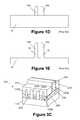
- FIGS. 1A-1Edepict one illustrative example of a prior art sidewall image transfer technique.
- a mandrel 12is formed above a structure 10 , such as a semiconducting substrate.
- the mandrel 12may be made of a variety of materials, e.g., amorphous silicon, polysilicon, etc.
- the size of the mandrel 12may vary depending upon the particular applications.
- the mandrel 12may be formed be depositing and patterning a layer of mandrel material using known deposition, photolithography and etching tools and techniques.
- a layer of spacer material 14is conformably deposited above the mandrel 12 and the structure 10 .
- the layer of spacer material 14may be comprised of a variety of materials such as, for example, silicon nitride, silicon dioxide, etc.
- an anisotropic etching processis performed to define spacers 14 A adjacent the mandrel 12 .
- the mandrel 12is removed by performing a selective etching process that leaves the spacers 14 A to act as masks in a subsequent etching process that defines feature 18 in the structure 10 , as depicted in FIG. 1E .
- the present disclosureis directed to various methods of patterning features in a structure, such as a layer of material used in forming integrated circuit devices or in a semiconducting substrate, using a multiple sidewall image transfer technique.
- the present disclosureis directed to various methods of patterning features in a structure such as a layer of material used in forming integrated circuit devices or in a semiconducting substrate using a multiple sidewall image transfer technique.
- the methodincludes forming a first mandrel above a structure, forming a plurality of first spacers adjacent the first mandrel, forming a plurality of second mandrels, wherein each of the second mandrels is formed adjacent one of the first spacers, and forming a plurality of second spacers, wherein each of the second spacers is formed adjacent one of the second mandrels.
- the methodalso includes the steps of performing at least one etching process to selectively remove the first mandrel and the second mandrels relative to the first spacers and the second spacers and thereby define an etch mask comprised of the first spacers and the second spacer and performing at least one etching process through the etch mask on the structure to define a plurality of features in the structure.
- a methodin another illustrative example, includes forming a first mandrel above a structure, forming a plurality of first spacers adjacent the first mandrel, wherein each of the first spacers have a first width, and forming a plurality of second mandrels, wherein each of the second mandrels is formed adjacent one of the first spacers.
- the methodincludes the additional steps of forming a plurality of second spacers, wherein each of the second spacers is formed adjacent one of the second mandrels and each of the second spacers has a second width that is different from the first width, performing at least one etching process to selectively remove the first mandrel and the second mandrels relative to the first spacers and the second spacers and thereby define an etch mask comprised of the first spacers and the second spacers, and performing at least one etching process through the etch mask on the structure to define a plurality of features in the structure.
- FIGS. 1A-1Edepict one illustrative example of a prior art sidewall image transfer technique
- FIGS. 2A-2Pdepict various illustrative methods disclosed herein for patterning features in a structure such as a layer of material used in forming features of an integrated circuit device or forming features in a semiconducting substrate;
- FIGS. 3A-3Cdepict one illustrative embodiment of a novel illustrative FinFET device that may be formed using the methods disclosed herein.
- the present disclosureis directed to various methods of patterning features in a structure such as a layer of material used in forming integrated circuit devices or in a semiconducting substrate using a multiple sidewall image transfer technique.
- a structuresuch as a layer of material used in forming integrated circuit devices or in a semiconducting substrate using a multiple sidewall image transfer technique.
- the present methodis applicable to a variety of devices, including, but not limited to, ASICs, logic devices, memory devices, etc.
- the present inventionmay be employed in forming any of a variety of different types of features formed on an integrated circuit product, such as lines, trenches, gate electrode structures, fins for FinFET devices, etc.
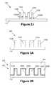
- FIGS. 2A-2Jdepict one illustrative method disclosed herein for forming various features on a structure used in the manufacture of integrated circuit devices.
- a first mandrel 112is formed above a structure 110 .
- the structure 110is intended to be representative of any type of structure or layer of material that may be employed in manufacturing integrated circuit products.
- the structure 110may be a semiconducting substrate, a layer of metal, a layer of silicon nitride, a layer of polysilicon, a layer of gate electrode material, etc.
- the first mandrel 112may be made of a variety of materials, e.g., amorphous silicon, polysilicon, etc.
- the size of the first mandrel 112may vary depending upon the particular applications.
- the first mandrel 112may have a height of about 80 nm and a width 112 W of about 40 nm.
- the first mandrel 112may be formed be depositing and patterning a layer of mandrel material using known deposition, photolithography and etching tools and techniques.
- a first layer of spacer material 114is conformably deposited above the first mandrel 112 and the structure 110 .
- the first layer of spacer material 114may be comprised of a variety of materials such as, for example, silicon nitride, silicon dioxide, etc.
- the thickness of the first layer of spacer material 114may vary depending upon the size of the features to be formed in the structure 110 , as described more fully below.
- an anisotropic etching processis performed on the first layer of spacer material 114 to define a plurality of first spacers 114 A adjacent the first mandrel 112 .
- the width 114 AW of the first spacers 114 Amay be about 10-25 nm.
- a layer of mandrel material 116is conformably deposited above the first mandrel 112 and the first spacers 114 A.
- the layer of mandrel material 116may be comprised of a variety of materials such as, for example, amorphous silicon, polysilicon, etc.
- the thickness of the layer of mandrel material 116may vary depending upon the size of the features to be formed in the structure 110 , as described more fully below.
- the layer of mandrel material 116may be made of the same material as the first mandrel 112 , although that is not required.
- an anisotropic etching processis performed on the layer of mandrel material 116 to define a plurality of second mandrels 116 A adjacent the first spacers 114 A.
- the second mandrels 116 Ahave a width 116 AW that may be the same as the width 112 W of the first mandrel 112 or they may have a different width, i.e., the width 116 AW may be wider or narrower than the width 112 W.
- the width 116 AW of the second mandrels 116 Amay be about 20-40 nm.
- a second layer of spacer material 118is conformably deposited above the various structures depicted in FIG. 2E .
- the second layer of spacer material 118may be comprised of a variety of materials such as, for example, silicon nitride, silicon dioxide, etc.
- the thickness of the second layer of spacer material 118may vary depending upon the size of the features to be formed in the structure 110 , as described more fully below.
- the second layer of spacer material 118may be made of the same material as the first layer of spacer material 114 , although that is not required.
- an anisotropic etching processis performed on the second layer of spacer material 118 to define a plurality of second spacers 118 A adjacent each of the second spacers 114 A.
- the width 118 AW of the second spacers 118 Amay be about 5-15 nm.
- the width 118 AW of the second spacers 118 Amay be different than the width 114 A of the first spacers 114 A so that features of different sizes may be formed in the structure 110 .
- the width 118 AW of the second spacers 118 Amay be approximately the same as or wider than the width 114 A of the first spacers 114 A.
- one or more etching processesis performed to selectively remove the first mandrel 112 and the second mandrels 116 relative to the first spacers 114 A and the second spacers 118 A.
- the first spacers 114 A and the second spacers 118 Adefine an etch mask 130 that may be employed in defining various features 120 in the structure 110 , as described more fully below.
- FIG. 2Ireflects the device after an etching process, either a wet or dry etching process, has been performed on the structure 110 through the mask layer 130 to define a plurality of features 120 in the structure 110 .
- a variety of different types of featuresmay be formed, e.g., lines, trenches, gate electrode structures, fins for FinFET devices, etc.
- the particular inventionshould not be considered as limited to any particular type of feature.
- a plurality of features 120 A, 120 Bare formed in the structure 110 .
- FIG. 2Jdepicts the device 100 after the mask layer 130 has been stripped.
- the features 120 A(corresponding to the first spacers 114 A) have a greater width 120 AW than the width 120 BW of the features 120 B (corresponding to the second spacers 118 A).
- FIGS. 2K-2Mdisclose another illustrative example wherein the methods disclosed herein may be employed.
- the width 119 of the second mandrels 116 Aare wider than the width 112 W of the first mandrel 112 , while the widths of the first spacers 114 A and the second spacers 118 A are the same.
- one or more etching processesare performed to selectively remove the first mandrel 112 and the second mandrels 116 relative to the first spacers 114 A and the second spacers 118 A.
- the first spacers 114 A and the second spacers 118 Adefine an etch mask 130 that may be employed in defining various features 120 in the structure 110 , as described more fully below.
- FIG. 2Mreflects the device 100 after an etching process, either a wet or dry etching process, has been performed on the structure 110 through the mask layer 130 to define a plurality of trench features 132 A, 132 B in the structure 110 .
- the trench 132 Ahas a width 112 W that corresponds to the width of the first mandrel 112
- the trenches 132 Bhave a width 119 that corresponds to the width of the second mandrels 116 A.
- FIGS. 2N-2Pdepict yet another illustrative example wherein the methods disclosed herein may be employed.
- the structure 110may be a layer of gate electrode material 142 that is formed above a gate insulation material layer 140 that is formed above a semiconducting substrate 150 .
- the first and second mandrels 112 , 116 Ahave the same width and the widths of the first spacers 114 A and the second spacers 118 A are the same. As shown in FIG.
- one or more etching processesis performed to selectively remove the first mandrel 112 and the second mandrels 116 relative to the first spacers 114 A and the second spacers 118 A.
- the first spacers 114 A and the second spacers 118 Adefine an etch mask 130 that may be employed in defining various features in the layer of gate electrode material 142 .
- FIG. 2Preflects the device 100 after one or more etching processes, either a wet or dry etching process, have been performed on at least the layer of gate electrode material 142 to define a plurality of gate electrodes 142 A.
- an etching processis also performed through the mask layer 130 do pattern the gate insulation material layer 140 and thereby define gate insulation layers 140 A.
- the methods disclosed hereinmay be employed to define a plurality of gate structures 160 for the device 100 , wherein the gate structures 160 are comprised of a gate insulation layer 140 A and a gate electrode 142 A.
- the gate electrodes 142 Ahave a critical dimension that corresponds to the width of the spacer positioned thereabove.
- FIGS. 3A-3Cdepict an illustrative example wherein the methods disclosed herein may be employed to form a FinFET device 200 , wherein the features 120 A, 120 B are fins of the FinFET device 200 .
- the features 120 A, 120 Bmay have different widths.
- the structure 110may be bulk silicon substrate or it may be the active layer of an SOI substrate.
- the overall size, shape and configuration of the fins 120 A, 120 Bmay vary depending on the particular application.
- FIG. 3Bdepicts the FinFET device 200 after several process operations have been performed.
- an illustrative gate electrode structure 202is formed for the device 200 using well known techniques.
- the schematically depicted gate structure 202includes an illustrative gate insulation layer 202 A and an illustrative gate electrode 202 B.
- An illustrative gate cap layer 204is also depicted as being formed above the illustrative gate electrode layer 202 B.
- the gate insulation layer 202 Amay be comprised of a variety of different materials, such as, for example, silicon dioxide, a so-called high-k (k greater than 10) insulation material, etc.
- the gate electrode 202 Bmay also be of a material such as polysilicon or amorphous silicon, or it may be comprised of one or more metal layers that act as the gate electrode 202 B.
- the gate structure 202 of the FinFET device 200 depicted in the drawingsi.e., the gate insulation layer 202 A and the gate electrode 202 B, is intended to be representative in nature. That is, the gate structure 202 may be comprised of a variety of different materials and it may they have a variety of configurations, and the gate structure 202 may be made using either so-called “gate-first” or “replacement metal gate” techniques.
- an oxidation processmay be performed to form the illustrative gate insulation layer 202 A comprised of silicon dioxide that is depicted in FIG. 3B .
- the gate electrode material and the gate cap layer materialmay be deposited above the device 200 and the layers may be patterned using known photolithographic and etching techniques.
- the gate cap layer 204may be made of a variety of materials such as, for example, silicon nitride.
- sidewall spacerscomprised of, for example, silicon nitride, are formed adjacent the gate electrode structure 202 to protect and electrically isolate the gate electrode structure 202 , however, such spacers are not shown in FIG. 3B so as not to obscure the inventions disclosed herein.
- FIG. 3Cis a schematic, perspective view of one illustrative embodiment of the FinFET device 200 at a later stage of fabrication wherein the illustrative fins 120 A, 120 B intentionally have different target widths, not differences in width due to manufacturing tolerances or errors.
- the channel width of the FinFET device 200may be varied as desired by device designers to achieve a desired or target drive current that is required for a particular circuit being designed. That is, using the techniques disclosed herein, a FinFET device may be designed and manufactured to produce a drive current that is different from a FinFET device with fins having a uniform thickness.
- another important parameter of the FinFET devicethat depends to at least some degree on the width of the fins is the threshold voltage.
- the device 200includes the gate structure 202 and the gate cap layer 204 .
- the gate insulation layer 202 Ais not present under the gate electrode 202 B.
- an insulating material 209is also depicted in FIG. 3C .
- sidewall spacers 208and a semiconducting material layer 210 where source/drain regions will be formed for the device 100 .
- the spacers 208may be formed form a variety of materials such as, for example, silicon nitride, silicon oxynitride, etc.
- the spacers 208may be made by conformably depositing a layer of spacer material and thereafter performing an anisotropic etching process. It should be understood that when it is stated in the claims that a spacer is formed adjacent a mandrel or vice-versa, physical contact between the spacer and the mandrel is not required. That is, for example, a liner layer may be formed on the first mandrel 112 prior to forming the first spacers 114 A on such a liner layer. In that case, the first spacers 114 A should still be understood as being formed adjacent to the first mandrel 112 . To the extent that physical contact between a spacer and a mandrel is set forth in the claims, that physical contact will be claimed by reciting that the spacer is formed “on” the mandrel—or vice versa.
Landscapes
- Engineering & Computer Science (AREA)
- Manufacturing & Machinery (AREA)
- Physics & Mathematics (AREA)
- Condensed Matter Physics & Semiconductors (AREA)
- General Physics & Mathematics (AREA)
- Computer Hardware Design (AREA)
- Microelectronics & Electronic Packaging (AREA)
- Power Engineering (AREA)
- Inorganic Chemistry (AREA)
- Chemical & Material Sciences (AREA)
- Thin Film Transistor (AREA)
- Semiconductor Memories (AREA)
- Insulated Gate Type Field-Effect Transistor (AREA)
Abstract
Description
Claims (22)
Priority Applications (6)
| Application Number | Priority Date | Filing Date | Title |
|---|---|---|---|
| US13/305,303US8557675B2 (en) | 2011-11-28 | 2011-11-28 | Methods of patterning features in a structure using multiple sidewall image transfer technique |
| SG2012081873ASG190521A1 (en) | 2011-11-28 | 2012-11-06 | Methods of patterning features in a structure using multiple sidewall image transfer technique |
| KR1020120131793AKR20130059275A (en) | 2011-11-28 | 2012-11-20 | Methods of patterning features in a structure using multiple sidewall image transfer technique |
| TW101144277ATWI509669B (en) | 2011-11-28 | 2012-11-27 | Method of patterning features in a structure using multiple sidewall image transfer techniques |
| DE102012221620ADE102012221620A1 (en) | 2011-11-28 | 2012-11-27 | A method of structuring features in a structure using a multi-sidewall image transfer technique |
| CN201210495454.1ACN103137459B (en) | 2011-11-28 | 2012-11-28 | Utilize the method for many sidewall image transfer technology patterned features in the structure |
Applications Claiming Priority (1)
| Application Number | Priority Date | Filing Date | Title |
|---|---|---|---|
| US13/305,303US8557675B2 (en) | 2011-11-28 | 2011-11-28 | Methods of patterning features in a structure using multiple sidewall image transfer technique |
Publications (2)
| Publication Number | Publication Date |
|---|---|
| US20130134486A1 US20130134486A1 (en) | 2013-05-30 |
| US8557675B2true US8557675B2 (en) | 2013-10-15 |
Family
ID=48288145
Family Applications (1)
| Application Number | Title | Priority Date | Filing Date |
|---|---|---|---|
| US13/305,303Active2032-01-09US8557675B2 (en) | 2011-11-28 | 2011-11-28 | Methods of patterning features in a structure using multiple sidewall image transfer technique |
Country Status (6)
| Country | Link |
|---|---|
| US (1) | US8557675B2 (en) |
| KR (1) | KR20130059275A (en) |
| CN (1) | CN103137459B (en) |
| DE (1) | DE102012221620A1 (en) |
| SG (1) | SG190521A1 (en) |
| TW (1) | TWI509669B (en) |
Cited By (14)
| Publication number | Priority date | Publication date | Assignee | Title |
|---|---|---|---|---|
| US20130154004A1 (en)* | 2011-12-16 | 2013-06-20 | Taiwan Semiconductor Manufacturing Company, LTD. ('TSMC') | Semiconductor device with biased feature |
| US20150014772A1 (en)* | 2013-07-11 | 2015-01-15 | International Business Machines Corporation | Patterning fins and planar areas in silicon |
| US8975129B1 (en)* | 2013-11-13 | 2015-03-10 | Taiwan Semiconductor Manufacturing Company, Ltd. | Method of making a FinFET device |
| US9269627B1 (en) | 2014-09-30 | 2016-02-23 | International Business Machines Corporation | Fin cut on SIT level |
| US9318478B1 (en) | 2015-01-30 | 2016-04-19 | Samsung Electronics Co., Ltd. | Semiconductor device and fabricating method thereof |
| US9330931B2 (en) | 2014-05-27 | 2016-05-03 | Samsung Electronics Co., Ltd. | Method of manufacturing semiconductor device |
| KR20160063212A (en)* | 2014-11-26 | 2016-06-03 | 삼성전자주식회사 | Method for fabricating semiconductor device |
| US9437497B2 (en) | 2013-10-18 | 2016-09-06 | Taiwan Semiconductor Manufacturing Company, Ltd. | Method of making a FinFET device |
| US9536744B1 (en) | 2015-12-17 | 2017-01-03 | International Business Machines Corporation | Enabling large feature alignment marks with sidewall image transfer patterning |
| US9601345B2 (en) | 2015-03-27 | 2017-03-21 | International Business Machines Corporation | Fin trimming in a double sit process |
| US9679815B2 (en) | 2015-04-15 | 2017-06-13 | Samsung Electronics Co., Ltd. | Semiconductor device and method of fabricating the same |
| US10475791B1 (en) | 2018-05-31 | 2019-11-12 | Globalfoundries Inc. | Transistor fins with different thickness gate dielectric |
| US20210119023A1 (en)* | 2019-10-17 | 2021-04-22 | Shanghai Huali Integrated Circuit Corporation | FinFET Transistor Cut Etching Process Method |
| US20220059445A1 (en)* | 2020-07-08 | 2022-02-24 | Changxin Memory Technologies, Inc. | Semiconductor structure and manufacturing method thereof |
Families Citing this family (21)
| Publication number | Priority date | Publication date | Assignee | Title |
|---|---|---|---|---|
| US8759194B2 (en) | 2012-04-25 | 2014-06-24 | International Business Machines Corporation | Device structures compatible with fin-type field-effect transistor technologies |
| US8669167B1 (en)* | 2012-08-28 | 2014-03-11 | International Business Machines Corporation | Techniques for metal gate workfunction engineering to enable multiple threshold voltage FINFET devices |
| US9177820B2 (en)* | 2012-10-24 | 2015-11-03 | Globalfoundries U.S. 2 Llc | Sub-lithographic semiconductor structures with non-constant pitch |
| US8716156B1 (en)* | 2013-02-01 | 2014-05-06 | Globalfoundries Inc. | Methods of forming fins for a FinFET semiconductor device using a mandrel oxidation process |
| US9412601B2 (en)* | 2013-03-15 | 2016-08-09 | Infineon Technologies Dresden Gmbh | Method for processing a carrier |
| US9711368B2 (en)* | 2013-04-15 | 2017-07-18 | United Microelectronics Corp. | Sidewall image transfer process |
| US9034723B1 (en)* | 2013-11-25 | 2015-05-19 | Taiwan Semiconductor Manufacturing Company, Ltd. | Method of making a FinFET device |
| US9136106B2 (en)* | 2013-12-19 | 2015-09-15 | Taiwan Semiconductor Manufacturing Company, Ltd. | Method for integrated circuit patterning |
| US9196485B2 (en) | 2014-02-25 | 2015-11-24 | International Business Machines Corporation | Stacked sidewall patterning |
| US9318334B2 (en)* | 2014-08-27 | 2016-04-19 | United Microelectronics Corp. | Method for fabricating semiconductor device |
| US9536739B2 (en) | 2014-10-28 | 2017-01-03 | International Business Machines Corporation | Self-cut sidewall image transfer process |
| CN105702726B (en)* | 2014-11-27 | 2019-01-18 | 中国科学院微电子研究所 | Semiconductor device and method for manufacturing the same |
| KR102327143B1 (en)* | 2015-03-03 | 2021-11-16 | 삼성전자주식회사 | Integrated circuit device |
| CN106033482B (en)* | 2015-03-18 | 2021-03-16 | 联华电子股份有限公司 | Method for generating layout patterns |
| KR102338363B1 (en)* | 2015-04-15 | 2021-12-09 | 삼성전자주식회사 | Semiconductor device and method of fabricating the same |
| WO2018125092A1 (en)* | 2016-12-28 | 2018-07-05 | Intel Corporation | Tight pitch by iterative spacer formation |
| US11557658B2 (en) | 2017-12-27 | 2023-01-17 | Intel Corporation | Transistors with high density channel semiconductor over dielectric material |
| TWI685086B (en) | 2019-01-03 | 2020-02-11 | 華邦電子股份有限公司 | Landing pad and method of manufacturing the same |
| CN111524886B (en)* | 2019-02-01 | 2023-06-09 | 华邦电子股份有限公司 | Landing pad structure and manufacturing method thereof |
| US11152377B2 (en)* | 2019-04-25 | 2021-10-19 | International Business Machines Corporation | Nanosheet SRAM by SIT process |
| US20220223743A1 (en)* | 2021-01-13 | 2022-07-14 | Taiwan Semiconductor Manufacturing Company, Ltd. | Overhanging source/drain contact |
Citations (33)
| Publication number | Priority date | Publication date | Assignee | Title |
|---|---|---|---|---|
| US4648937A (en) | 1985-10-30 | 1987-03-10 | International Business Machines Corporation | Method of preventing asymmetric etching of lines in sub-micrometer range sidewall images transfer |
| US4689869A (en) | 1986-04-07 | 1987-09-01 | International Business Machines Corporation | Fabrication of insulated gate gallium arsenide FET with self-aligned source/drain and submicron channel length |
| US4808545A (en) | 1987-04-20 | 1989-02-28 | International Business Machines Corporation | High speed GaAs MESFET having refractory contacts and a self-aligned cold gate fabrication process |
| US5460991A (en) | 1995-03-16 | 1995-10-24 | United Microelectronics Corporation | Method of making high coupling ratio flash EEPROM device |
| US5885425A (en) | 1995-06-06 | 1999-03-23 | International Business Machines Corporation | Method for selective material deposition on one side of raised or recessed features |
| US6566759B1 (en) | 1999-08-23 | 2003-05-20 | International Business Machines Corporation | Self-aligned contact areas for sidewall image transfer formed conductors |
| US6875703B1 (en) | 2004-01-20 | 2005-04-05 | International Business Machines Corporation | Method for forming quadruple density sidewall image transfer (SIT) structures |
| US20060046382A1 (en) | 2004-08-26 | 2006-03-02 | Kuk-Han Yoon | Method of forming a capacitor for a semiconductor device |
| US20060084243A1 (en) | 2004-10-20 | 2006-04-20 | Ying Zhang | Oxidation sidewall image transfer patterning method |
| US7265013B2 (en) | 2005-09-19 | 2007-09-04 | International Business Machines Corporation | Sidewall image transfer (SIT) technologies |
| US7301210B2 (en) | 2006-01-12 | 2007-11-27 | International Business Machines Corporation | Method and structure to process thick and thin fins and variable fin to fin spacing |
| US20070284669A1 (en) | 2004-05-25 | 2007-12-13 | Abadeer Wagdi W | Method and structure to process thick and thin fins and variable fin to fin spacing |
| US7381655B2 (en) | 2005-09-14 | 2008-06-03 | International Business Machines Corporation | Mandrel/trim alignment in SIT processing |
| US7439144B2 (en) | 2006-02-16 | 2008-10-21 | International Business Machines Corporation | CMOS gate structures fabricated by selective oxidation |
| US20080315746A1 (en) | 2003-09-05 | 2008-12-25 | Dharam Pal Gosain | Method of Manufacturing Fine Structure, Fine Structure, Display Unit, Method of Manufacturing Recoding Device, and Recoding Device |
| US7470570B2 (en) | 2006-11-14 | 2008-12-30 | International Business Machines Corporation | Process for fabrication of FinFETs |
| US20090090975A1 (en) | 2007-10-09 | 2009-04-09 | Chartered Semiconductor Manufacturing Ltd. | Integrated circuit system employing fluorine doping |
| US20090309162A1 (en)* | 2008-06-17 | 2009-12-17 | Infineon Technologies Ag. | Semiconductor device having different fin widths |
| US7699996B2 (en) | 2007-02-28 | 2010-04-20 | International Business Machines Corporation | Sidewall image transfer processes for forming multiple line-widths |
| US7847323B2 (en) | 2005-10-07 | 2010-12-07 | International Business Machines Corporation | Methods for fabricating a semiconductor structure using a mandrel and semiconductor structures formed thereby |
| US20110014791A1 (en)* | 2009-02-04 | 2011-01-20 | Globalfoundries Inc. | Methods for fabricating finfet structures having different channel lengths |
| US20110021010A1 (en)* | 2009-07-27 | 2011-01-27 | International Business Machines Corporation | Method for double pattern density |
| US20110113393A1 (en) | 2009-11-09 | 2011-05-12 | Cadence Design Systems, Inc. | Method, system, and program product for routing an integrated circuit to be manufactured by sidewall-image transfer |
| US20110111596A1 (en) | 2009-11-06 | 2011-05-12 | International Business Machine Corporation | Sidewall Image Transfer Using the Lithographic Stack as the Mandrel |
| US20110117743A1 (en)* | 2005-03-15 | 2011-05-19 | Round Rock Research, Llc | Multiple deposition for integration of spacers in pitch multiplication process |
| US7972959B2 (en) | 2008-12-01 | 2011-07-05 | Applied Materials, Inc. | Self aligned double patterning flow with non-sacrificial features |
| US7989355B2 (en) | 2009-02-12 | 2011-08-02 | Taiwan Semiconductor Manufacturing Company, Ltd. | Method of pitch halving |
| US7998357B2 (en) | 2008-03-28 | 2011-08-16 | Samsung Electronics Co., Ltd. | Method of fine patterning semiconductor device |
| US8003236B2 (en) | 2008-06-17 | 2011-08-23 | Hitachi Global Storage Technologies Netherlands B.V. | Method for making a master mold with high bit-aspect-ratio for nanoimprinting patterned magnetic recording disks, master mold made by the method, and disk imprinted by the master mold |
| US8084310B2 (en) | 2008-10-23 | 2011-12-27 | Applied Materials, Inc. | Self-aligned multi-patterning for advanced critical dimension contacts |
| US20120122315A1 (en) | 2010-11-11 | 2012-05-17 | International Business Machines Corporation | Self-aligned devices and methods of manufacture |
| US20120258587A1 (en) | 2011-04-07 | 2012-10-11 | The Government Of The United States Of America, As Represented By The Secretary Of The Navy | Method of Forming Graphene on a Surface |
| US8389383B1 (en) | 2011-04-05 | 2013-03-05 | Micron Technology, Inc. | Patterned semiconductor bases, and patterning methods |
Family Cites Families (2)
| Publication number | Priority date | Publication date | Assignee | Title |
|---|---|---|---|---|
| CN101295647A (en)* | 2008-01-16 | 2008-10-29 | 清华大学 | A Method of Enhancing Strain in Channel Region of MOS Devices |
| US7829951B2 (en)* | 2008-11-06 | 2010-11-09 | Qualcomm Incorporated | Method of fabricating a fin field effect transistor (FinFET) device |
- 2011
- 2011-11-28USUS13/305,303patent/US8557675B2/enactiveActive
- 2012
- 2012-11-06SGSG2012081873Apatent/SG190521A1/enunknown
- 2012-11-20KRKR1020120131793Apatent/KR20130059275A/ennot_activeWithdrawn
- 2012-11-27DEDE102012221620Apatent/DE102012221620A1/ennot_activeCeased
- 2012-11-27TWTW101144277Apatent/TWI509669B/ennot_activeIP Right Cessation
- 2012-11-28CNCN201210495454.1Apatent/CN103137459B/ennot_activeExpired - Fee Related
Patent Citations (39)
| Publication number | Priority date | Publication date | Assignee | Title |
|---|---|---|---|---|
| US4648937A (en) | 1985-10-30 | 1987-03-10 | International Business Machines Corporation | Method of preventing asymmetric etching of lines in sub-micrometer range sidewall images transfer |
| US4689869A (en) | 1986-04-07 | 1987-09-01 | International Business Machines Corporation | Fabrication of insulated gate gallium arsenide FET with self-aligned source/drain and submicron channel length |
| US4808545A (en) | 1987-04-20 | 1989-02-28 | International Business Machines Corporation | High speed GaAs MESFET having refractory contacts and a self-aligned cold gate fabrication process |
| US5460991A (en) | 1995-03-16 | 1995-10-24 | United Microelectronics Corporation | Method of making high coupling ratio flash EEPROM device |
| US5885425A (en) | 1995-06-06 | 1999-03-23 | International Business Machines Corporation | Method for selective material deposition on one side of raised or recessed features |
| US6566759B1 (en) | 1999-08-23 | 2003-05-20 | International Business Machines Corporation | Self-aligned contact areas for sidewall image transfer formed conductors |
| US20030115750A1 (en) | 1999-08-23 | 2003-06-26 | International Business Machines Corporation | Self-aligned contact areas for sidewall image transfer formed conductors |
| US6949458B2 (en) | 1999-08-23 | 2005-09-27 | International Business Machines Corporation | Self-aligned contact areas for sidewall image transfer formed conductors |
| US20080315746A1 (en) | 2003-09-05 | 2008-12-25 | Dharam Pal Gosain | Method of Manufacturing Fine Structure, Fine Structure, Display Unit, Method of Manufacturing Recoding Device, and Recoding Device |
| US6875703B1 (en) | 2004-01-20 | 2005-04-05 | International Business Machines Corporation | Method for forming quadruple density sidewall image transfer (SIT) structures |
| US20070284669A1 (en) | 2004-05-25 | 2007-12-13 | Abadeer Wagdi W | Method and structure to process thick and thin fins and variable fin to fin spacing |
| US7763531B2 (en) | 2004-05-25 | 2010-07-27 | International Business Machines Corporation | Method and structure to process thick and thin fins and variable fin to fin spacing |
| US20060046382A1 (en) | 2004-08-26 | 2006-03-02 | Kuk-Han Yoon | Method of forming a capacitor for a semiconductor device |
| US20060084243A1 (en) | 2004-10-20 | 2006-04-20 | Ying Zhang | Oxidation sidewall image transfer patterning method |
| US20110117743A1 (en)* | 2005-03-15 | 2011-05-19 | Round Rock Research, Llc | Multiple deposition for integration of spacers in pitch multiplication process |
| US7381655B2 (en) | 2005-09-14 | 2008-06-03 | International Business Machines Corporation | Mandrel/trim alignment in SIT processing |
| US20080188080A1 (en) | 2005-09-14 | 2008-08-07 | International Business Machines Corporation | Mandrel/trim alignment in sit processing |
| US7265013B2 (en) | 2005-09-19 | 2007-09-04 | International Business Machines Corporation | Sidewall image transfer (SIT) technologies |
| US7847323B2 (en) | 2005-10-07 | 2010-12-07 | International Business Machines Corporation | Methods for fabricating a semiconductor structure using a mandrel and semiconductor structures formed thereby |
| US7301210B2 (en) | 2006-01-12 | 2007-11-27 | International Business Machines Corporation | Method and structure to process thick and thin fins and variable fin to fin spacing |
| US7439144B2 (en) | 2006-02-16 | 2008-10-21 | International Business Machines Corporation | CMOS gate structures fabricated by selective oxidation |
| US20080286971A1 (en) | 2006-02-16 | 2008-11-20 | International Business Machines Corporation | CMOS Gate Structures Fabricated by Selective Oxidation |
| US7470570B2 (en) | 2006-11-14 | 2008-12-30 | International Business Machines Corporation | Process for fabrication of FinFETs |
| US20090101995A1 (en) | 2006-11-14 | 2009-04-23 | International Business Machines Corporation | PROCESS FOR FABRICATION OF FINFETs |
| US7699996B2 (en) | 2007-02-28 | 2010-04-20 | International Business Machines Corporation | Sidewall image transfer processes for forming multiple line-widths |
| US20090090975A1 (en) | 2007-10-09 | 2009-04-09 | Chartered Semiconductor Manufacturing Ltd. | Integrated circuit system employing fluorine doping |
| US7998357B2 (en) | 2008-03-28 | 2011-08-16 | Samsung Electronics Co., Ltd. | Method of fine patterning semiconductor device |
| US20090309162A1 (en)* | 2008-06-17 | 2009-12-17 | Infineon Technologies Ag. | Semiconductor device having different fin widths |
| US8003236B2 (en) | 2008-06-17 | 2011-08-23 | Hitachi Global Storage Technologies Netherlands B.V. | Method for making a master mold with high bit-aspect-ratio for nanoimprinting patterned magnetic recording disks, master mold made by the method, and disk imprinted by the master mold |
| US8084310B2 (en) | 2008-10-23 | 2011-12-27 | Applied Materials, Inc. | Self-aligned multi-patterning for advanced critical dimension contacts |
| US7972959B2 (en) | 2008-12-01 | 2011-07-05 | Applied Materials, Inc. | Self aligned double patterning flow with non-sacrificial features |
| US20110014791A1 (en)* | 2009-02-04 | 2011-01-20 | Globalfoundries Inc. | Methods for fabricating finfet structures having different channel lengths |
| US7989355B2 (en) | 2009-02-12 | 2011-08-02 | Taiwan Semiconductor Manufacturing Company, Ltd. | Method of pitch halving |
| US20110021010A1 (en)* | 2009-07-27 | 2011-01-27 | International Business Machines Corporation | Method for double pattern density |
| US20110111596A1 (en) | 2009-11-06 | 2011-05-12 | International Business Machine Corporation | Sidewall Image Transfer Using the Lithographic Stack as the Mandrel |
| US20110113393A1 (en) | 2009-11-09 | 2011-05-12 | Cadence Design Systems, Inc. | Method, system, and program product for routing an integrated circuit to be manufactured by sidewall-image transfer |
| US20120122315A1 (en) | 2010-11-11 | 2012-05-17 | International Business Machines Corporation | Self-aligned devices and methods of manufacture |
| US8389383B1 (en) | 2011-04-05 | 2013-03-05 | Micron Technology, Inc. | Patterned semiconductor bases, and patterning methods |
| US20120258587A1 (en) | 2011-04-07 | 2012-10-11 | The Government Of The United States Of America, As Represented By The Secretary Of The Navy | Method of Forming Graphene on a Surface |
Non-Patent Citations (8)
| Title |
|---|
| Chen et al., "Mandrel and Spacer Engineering Based Self-aligned Triple Patterning," Proc. of SPIE, vol. 8328, Apr. 16, 2012. |
| Chen et al., "Self-Aligned Triple Patterning for Continuous IC Scaling to Half-Pitch 15nm," Proc. of SPIE, vol. 7973, Mar. 22, 2011. |
| Chen et al., "Self-Aligned Triple Patterning to Extend Optical Lithography for 1× Patterning," Presentation from International Symposium on Lithography Extensions, Oct. 21, 2010. |
| Mebarki et al., "Innovative Self-Aligned Triple Patterning for 1× half pitch using Single 'Spacer Deposition-Spacer Etch step," Proc. of SPIE, vol. 7973, Mar. 22, 2011. |
| Medeiros D., "Lithograph on the Edge", 6th International Symposium on Immersion Lithography Extensions, Prague Czech Republic, Oct. 23, 2009.* |
| Sematech Panel Discussion downloaded from URL <http://www.sematech.org/meetings/archives/litho/8065/pres/D3%20Panel%20Discussion.pdf> on Feb. 20, 2013.* |
| Sematech Panel Discussion downloaded from URL on Feb. 20, 2013.* |
| Zimmerman, "Double patterning lithography: double the trouble or double the fun?," SPIE Newsroom, 2009. |
Cited By (24)
| Publication number | Priority date | Publication date | Assignee | Title |
|---|---|---|---|---|
| US9059001B2 (en)* | 2011-12-16 | 2015-06-16 | Taiwan Semiconductor Manufacturing Company, Ltd. | Semiconductor device with biased feature |
| US20130154004A1 (en)* | 2011-12-16 | 2013-06-20 | Taiwan Semiconductor Manufacturing Company, LTD. ('TSMC') | Semiconductor device with biased feature |
| US9607835B2 (en) | 2011-12-16 | 2017-03-28 | Taiwan Semiconductor Manufacturing Company, Ltd. | Semiconductor device with biased feature |
| US20150014772A1 (en)* | 2013-07-11 | 2015-01-15 | International Business Machines Corporation | Patterning fins and planar areas in silicon |
| US9437497B2 (en) | 2013-10-18 | 2016-09-06 | Taiwan Semiconductor Manufacturing Company, Ltd. | Method of making a FinFET device |
| US11081394B2 (en) | 2013-10-18 | 2021-08-03 | Taiwan Semiconductor Manufacturing Company, Ltd. | Method of making a FinFET device |
| US10096519B2 (en) | 2013-10-18 | 2018-10-09 | Taiwan Semiconductor Manufacturing Company, Ltd. | Method of making a FinFET device |
| US8975129B1 (en)* | 2013-11-13 | 2015-03-10 | Taiwan Semiconductor Manufacturing Company, Ltd. | Method of making a FinFET device |
| US9330931B2 (en) | 2014-05-27 | 2016-05-03 | Samsung Electronics Co., Ltd. | Method of manufacturing semiconductor device |
| US9659931B2 (en) | 2014-09-30 | 2017-05-23 | International Business Machines Corporation | Fin cut on sit level |
| US9269627B1 (en) | 2014-09-30 | 2016-02-23 | International Business Machines Corporation | Fin cut on SIT level |
| US10038077B2 (en)* | 2014-11-26 | 2018-07-31 | Samsung Electronics Co., Ltd. | Method for fabricating semiconductor device |
| KR20160063212A (en)* | 2014-11-26 | 2016-06-03 | 삼성전자주식회사 | Method for fabricating semiconductor device |
| US20160380084A1 (en)* | 2014-11-26 | 2016-12-29 | Samsung Electronics Co., Ltd. | Method for fabricating semiconductor device |
| KR102279856B1 (en) | 2014-11-26 | 2021-07-20 | 삼성전자주식회사 | Method for fabricating semiconductor device |
| US9318478B1 (en) | 2015-01-30 | 2016-04-19 | Samsung Electronics Co., Ltd. | Semiconductor device and fabricating method thereof |
| US9601345B2 (en) | 2015-03-27 | 2017-03-21 | International Business Machines Corporation | Fin trimming in a double sit process |
| US9679815B2 (en) | 2015-04-15 | 2017-06-13 | Samsung Electronics Co., Ltd. | Semiconductor device and method of fabricating the same |
| US9536744B1 (en) | 2015-12-17 | 2017-01-03 | International Business Machines Corporation | Enabling large feature alignment marks with sidewall image transfer patterning |
| US10475791B1 (en) | 2018-05-31 | 2019-11-12 | Globalfoundries Inc. | Transistor fins with different thickness gate dielectric |
| US20210119023A1 (en)* | 2019-10-17 | 2021-04-22 | Shanghai Huali Integrated Circuit Corporation | FinFET Transistor Cut Etching Process Method |
| US11637194B2 (en)* | 2019-10-17 | 2023-04-25 | Shanghai Huali Integrated Circuit Corporation | FinFET transistor cut etching process method |
| US20220059445A1 (en)* | 2020-07-08 | 2022-02-24 | Changxin Memory Technologies, Inc. | Semiconductor structure and manufacturing method thereof |
| US12027456B2 (en)* | 2020-07-08 | 2024-07-02 | Changxin Memory Technologies, Inc. | Semiconductor structure and manufacturing method thereof |
Also Published As
| Publication number | Publication date |
|---|---|
| US20130134486A1 (en) | 2013-05-30 |
| TW201331996A (en) | 2013-08-01 |
| DE102012221620A1 (en) | 2013-05-29 |
| TWI509669B (en) | 2015-11-21 |
| KR20130059275A (en) | 2013-06-05 |
| SG190521A1 (en) | 2013-06-28 |
| CN103137459B (en) | 2015-09-23 |
| CN103137459A (en) | 2013-06-05 |
Similar Documents
| Publication | Publication Date | Title |
|---|---|---|
| US8557675B2 (en) | Methods of patterning features in a structure using multiple sidewall image transfer technique | |
| US9214360B2 (en) | Methods of patterning features having differing widths | |
| US9171764B2 (en) | Methods for fabricating integrated circuits using self-aligned quadruple patterning | |
| US9064932B1 (en) | Methods of forming gate structures by a gate-cut-last process and the resulting structures | |
| US9799748B1 (en) | Method of forming inner spacers on a nano-sheet/wire device | |
| US20130244437A1 (en) | Methods of forming features on an integrated circuit product using a novel compound sidewall image transfer technique | |
| CN107845578B (en) | Methods of forming vertical transistor devices | |
| CN108807545B (en) | Semiconductor device with a plurality of semiconductor chips | |
| US9449835B2 (en) | Methods of forming features having differing pitch spacing and critical dimensions | |
| US8741701B2 (en) | Fin structure formation including partial spacer removal | |
| US20160351411A1 (en) | Hybrid fin cutting processes for finfet semiconductor devices | |
| US9735060B1 (en) | Hybrid fin cut etching processes for products comprising tapered and non-tapered FinFET semiconductor devices | |
| US9543416B2 (en) | Methods of forming products with FinFET semiconductor devices without removing fins in certain areas of the product | |
| US9754792B1 (en) | Fin cutting process for manufacturing FinFET semiconductor devices | |
| US9378973B1 (en) | Method of using sidewall image transfer process to form fin-shaped structures | |
| US9887135B1 (en) | Methods for providing variable feature widths in a self-aligned spacer-mask patterning process | |
| US9847418B1 (en) | Methods of forming fin cut regions by oxidizing fin portions | |
| US9502308B1 (en) | Methods for forming transistor devices with different source/drain contact liners and the resulting devices | |
| US9023696B2 (en) | Method of forming contacts for devices with multiple stress liners | |
| US9711503B2 (en) | Gate structures with protected end surfaces to eliminate or reduce unwanted EPI material growth | |
| US8778772B2 (en) | Method of forming transistor with increased gate width | |
| US10204784B1 (en) | Methods of forming features on integrated circuit products | |
| US9793169B1 (en) | Methods for forming mask layers using a flowable carbon-containing silicon dioxide material | |
| US20130175577A1 (en) | NFET Device with Tensile Stressed Channel Region and Methods of Forming Same | |
| US10777463B2 (en) | Formation of epi source/drain material on transistor devices and the resulting structures |
Legal Events
| Date | Code | Title | Description |
|---|---|---|---|
| AS | Assignment | Owner name:GLOBALFOUNDRIES INC., CAYMAN ISLANDS Free format text:ASSIGNMENT OF ASSIGNORS INTEREST;ASSIGNOR:LICAUSI, NICHOLAS V.;REEL/FRAME:027294/0725 Effective date:20111102 | |
| STCF | Information on status: patent grant | Free format text:PATENTED CASE | |
| FPAY | Fee payment | Year of fee payment:4 | |
| AS | Assignment | Owner name:WILMINGTON TRUST, NATIONAL ASSOCIATION, DELAWARE Free format text:SECURITY AGREEMENT;ASSIGNOR:GLOBALFOUNDRIES INC.;REEL/FRAME:049490/0001 Effective date:20181127 | |
| AS | Assignment | Owner name:GLOBALFOUNDRIES U.S. INC., CALIFORNIA Free format text:ASSIGNMENT OF ASSIGNORS INTEREST;ASSIGNOR:GLOBALFOUNDRIES INC.;REEL/FRAME:054633/0001 Effective date:20201022 | |
| AS | Assignment | Owner name:GLOBALFOUNDRIES INC., CAYMAN ISLANDS Free format text:RELEASE BY SECURED PARTY;ASSIGNOR:WILMINGTON TRUST, NATIONAL ASSOCIATION;REEL/FRAME:054636/0001 Effective date:20201117 | |
| MAFP | Maintenance fee payment | Free format text:PAYMENT OF MAINTENANCE FEE, 8TH YEAR, LARGE ENTITY (ORIGINAL EVENT CODE: M1552); ENTITY STATUS OF PATENT OWNER: LARGE ENTITY Year of fee payment:8 | |
| AS | Assignment | Owner name:GLOBALFOUNDRIES U.S. INC., NEW YORK Free format text:RELEASE BY SECURED PARTY;ASSIGNOR:WILMINGTON TRUST, NATIONAL ASSOCIATION;REEL/FRAME:056987/0001 Effective date:20201117 | |
| FEPP | Fee payment procedure | Free format text:MAINTENANCE FEE REMINDER MAILED (ORIGINAL EVENT CODE: REM.); ENTITY STATUS OF PATENT OWNER: LARGE ENTITY |