US8556430B2 - Servo feedback control based on designated scanning servo beam in scanning beam display systems with light-emitting screens - Google Patents
Servo feedback control based on designated scanning servo beam in scanning beam display systems with light-emitting screensDownload PDFInfo
- Publication number
- US8556430B2 US8556430B2US12/643,623US64362309AUS8556430B2US 8556430 B2US8556430 B2US 8556430B2US 64362309 AUS64362309 AUS 64362309AUS 8556430 B2US8556430 B2US 8556430B2
- Authority
- US
- United States
- Prior art keywords
- servo
- screen
- light
- excitation
- scanning
- Prior art date
- Legal status (The legal status is an assumption and is not a legal conclusion. Google has not performed a legal analysis and makes no representation as to the accuracy of the status listed.)
- Active, expires
Links
Images


Classifications
- H—ELECTRICITY
- H04—ELECTRIC COMMUNICATION TECHNIQUE
- H04N—PICTORIAL COMMUNICATION, e.g. TELEVISION
- H04N9/00—Details of colour television systems
- H04N9/12—Picture reproducers
- H04N9/31—Projection devices for colour picture display, e.g. using electronic spatial light modulators [ESLM]
- H04N9/3129—Projection devices for colour picture display, e.g. using electronic spatial light modulators [ESLM] scanning a light beam on the display screen
- H04N9/3135—Driving therefor
- G—PHYSICS
- G01—MEASURING; TESTING
- G01J—MEASUREMENT OF INTENSITY, VELOCITY, SPECTRAL CONTENT, POLARISATION, PHASE OR PULSE CHARACTERISTICS OF INFRARED, VISIBLE OR ULTRAVIOLET LIGHT; COLORIMETRY; RADIATION PYROMETRY
- G01J3/00—Spectrometry; Spectrophotometry; Monochromators; Measuring colours
- G01J3/46—Measurement of colour; Colour measuring devices, e.g. colorimeters
- G01J3/50—Measurement of colour; Colour measuring devices, e.g. colorimeters using electric radiation detectors
- G01J3/506—Measurement of colour; Colour measuring devices, e.g. colorimeters using electric radiation detectors measuring the colour produced by screens, monitors, displays or CRTs
- G—PHYSICS
- G02—OPTICS
- G02B—OPTICAL ELEMENTS, SYSTEMS OR APPARATUS
- G02B26/00—Optical devices or arrangements for the control of light using movable or deformable optical elements
- G02B26/08—Optical devices or arrangements for the control of light using movable or deformable optical elements for controlling the direction of light
- G02B26/10—Scanning systems
- G02B26/101—Scanning systems with both horizontal and vertical deflecting means, e.g. raster or XY scanners
- G—PHYSICS
- G02—OPTICS
- G02B—OPTICAL ELEMENTS, SYSTEMS OR APPARATUS
- G02B26/00—Optical devices or arrangements for the control of light using movable or deformable optical elements
- G02B26/08—Optical devices or arrangements for the control of light using movable or deformable optical elements for controlling the direction of light
- G02B26/10—Scanning systems
- G02B26/105—Scanning systems with one or more pivoting mirrors or galvano-mirrors
- G—PHYSICS
- G02—OPTICS
- G02B—OPTICAL ELEMENTS, SYSTEMS OR APPARATUS
- G02B26/00—Optical devices or arrangements for the control of light using movable or deformable optical elements
- G02B26/08—Optical devices or arrangements for the control of light using movable or deformable optical elements for controlling the direction of light
- G02B26/10—Scanning systems
- G02B26/12—Scanning systems using multifaceted mirrors
- G02B26/123—Multibeam scanners, e.g. using multiple light sources or beam splitters
- G—PHYSICS
- G02—OPTICS
- G02B—OPTICAL ELEMENTS, SYSTEMS OR APPARATUS
- G02B26/00—Optical devices or arrangements for the control of light using movable or deformable optical elements
- G02B26/08—Optical devices or arrangements for the control of light using movable or deformable optical elements for controlling the direction of light
- G02B26/10—Scanning systems
- G02B26/12—Scanning systems using multifaceted mirrors
- G02B26/127—Adaptive control of the scanning light beam, e.g. using the feedback from one or more detectors
- G—PHYSICS
- G03—PHOTOGRAPHY; CINEMATOGRAPHY; ANALOGOUS TECHNIQUES USING WAVES OTHER THAN OPTICAL WAVES; ELECTROGRAPHY; HOLOGRAPHY
- G03B—APPARATUS OR ARRANGEMENTS FOR TAKING PHOTOGRAPHS OR FOR PROJECTING OR VIEWING THEM; APPARATUS OR ARRANGEMENTS EMPLOYING ANALOGOUS TECHNIQUES USING WAVES OTHER THAN OPTICAL WAVES; ACCESSORIES THEREFOR
- G03B21/00—Projectors or projection-type viewers; Accessories therefor
- G03B21/54—Accessories
- G03B21/56—Projection screens
- G03B21/567—Projection screens for colour projection
- G—PHYSICS
- G03—PHOTOGRAPHY; CINEMATOGRAPHY; ANALOGOUS TECHNIQUES USING WAVES OTHER THAN OPTICAL WAVES; ELECTROGRAPHY; HOLOGRAPHY
- G03B—APPARATUS OR ARRANGEMENTS FOR TAKING PHOTOGRAPHS OR FOR PROJECTING OR VIEWING THEM; APPARATUS OR ARRANGEMENTS EMPLOYING ANALOGOUS TECHNIQUES USING WAVES OTHER THAN OPTICAL WAVES; ACCESSORIES THEREFOR
- G03B21/00—Projectors or projection-type viewers; Accessories therefor
- G03B21/54—Accessories
- G03B21/56—Projection screens
- G03B21/60—Projection screens characterised by the nature of the surface
- G—PHYSICS
- G01—MEASURING; TESTING
- G01J—MEASUREMENT OF INTENSITY, VELOCITY, SPECTRAL CONTENT, POLARISATION, PHASE OR PULSE CHARACTERISTICS OF INFRARED, VISIBLE OR ULTRAVIOLET LIGHT; COLORIMETRY; RADIATION PYROMETRY
- G01J3/00—Spectrometry; Spectrophotometry; Monochromators; Measuring colours
- G01J3/46—Measurement of colour; Colour measuring devices, e.g. colorimeters
- G01J3/50—Measurement of colour; Colour measuring devices, e.g. colorimeters using electric radiation detectors
- G01J3/51—Measurement of colour; Colour measuring devices, e.g. colorimeters using electric radiation detectors using colour filters
- G01J3/513—Measurement of colour; Colour measuring devices, e.g. colorimeters using electric radiation detectors using colour filters having fixed filter-detector pairs
Definitions
- This patent applicationrelates to scanning-beam display systems.
- an optical beamcan be scanned over a screen to form images on the screen.
- Many display systemssuch as laser display systems use a polygon scanner with multiple reflective facets to provide horizontal scanning and a vertical scanning mirror such as a galvo-driven mirror to provide vertical scanning.
- a polygon scannerwith multiple reflective facets to provide horizontal scanning and a vertical scanning mirror such as a galvo-driven mirror to provide vertical scanning.
- one facet of the polygon scannerscans one horizontal line as the polygon scanner spins to change the orientation and position of the facet and the next facet scans the next horizontal line.
- the horizontal scanning and the vertical scanningare synchronized to each other to project images on the screen.
- This patent applicationdescribes, among others, implementations of display systems and devices based on scanning light on a light-emitting screen under optical excitation.
- the described display systemsuse light-emitting screens under optical excitation and at least one excitation optical beam to excite one or more light-emitting materials on a screen which emit light to form images.
- Servo control mechanisms for such display systemsare described based on a designated servo beam that is scanned over the screen by the same scanning module that scans the image-carrying excitation optical beam.
- This designated servo beamis used to provide servo feedback control over the scanning excitation beam to ensure proper optical alignment and accurate delivery of optical pulses in the excitation beam during normal display operation.
- multiple laserscan be used to simultaneously scan multiple excitation laser beams on the screen. For example, the multiple laser beams can illuminate one screen segment at a time and sequentially scan multiple screen segments to complete a full screen.
- a scanning beam display systemincludes a light module to direct and scan at least one excitation beam having optical pulses that carry image information and at least one servo beam at a servo beam wavelength different from a wavelength of the excitation beam; a screen positioned to receive the scanning excitation beam and the servo beam and comprising a light-emitting layer of parallel light-emitting stripes which absorb light of the excitation beam to emit visible light to produce images carried by the scanning excitation beam, the screen configured to reflect light of the servo beam towards the light module to produce servo feedback light; and an optical servo sensor module positioned to receive the servo feedback light and to produce a servo feedback signal indicative of positioning of the servo beam on the screen.
- the light moduleis responsive to the positioning of the servo beam on the screen in the servo feedback signal to adjust timing of the optical pulses carried by the scanning excitation beam to control the spatial alignment of spatial positions of the optical pulses in the excitation beam on the screen.
- the screen in the above systemcan include servo feedback marks that have facets facing the excitation light source that are specularly reflective to light of the servo beam, and areas outside the servo feedback marks that are diffusively reflective to light of the servo beam.
- the systemincludes a Fresnel lens located between the screen and the light module to direct the scanning servo beam and excitation beam to be at a substantially normal incidence to the screen.
- the Fresnel lenshas an optic axis symmetrically in a center of the Fresnel lens to be parallel to and offset from an optic axis of the light module to direct light of the servo beam that is specularly reflected by a servo feedback mark into the optical servo sensor while light of the servo beam that is diffusely reflected by the screen outside a servo feedback mark is spread by the Frensnel lens over an area greater than the optical servo sensor to direct a fraction of diffusely reflected light of the servo beam into the optical servo sensor.
- a method for controlling a scanning beam display systemincludes scanning one or more excitation beams modulated with optical pulses to carry images on a screen to excite parallel light-emitting strips to emit visible light which forms the images; scanning a servo beam at an optical wavelength different from an optical wavelength of the one or more excitation beams, on the screen; detecting light of the servo beam from the screen to obtain a servo signal indicative of positioning of the servo beam on the screen; and, in response to the positioning of the servo beam on the screen, controlling the one or more scanning excitation beams to control the spatial alignment of spatial positions of the optical pulses in each excitation beam on the screen.
- a scanning beam display systemincludes an excitation light source to produce at least one excitation beam having optical pulses that carry image information; a servo light source to produce at least one servo beam at a servo beam wavelength that is invisible; a beam scanning module to receive the excitation beam and the servo beam and to scan the excitation beam and the servo beam; and a light-emitting screen positioned to receive the scanning excitation beam and the servo beam.
- the screenincludes a light-emitting area which comprises (1) parallel light-emitting stripes which absorb light of the excitation beam to emit visible light to produce images carried by the scanning excitation beam, and (2) stripe dividers parallel to and spatially interleaved with the light-emitting stripes with each stripe divider being located between two adjacent stripes.
- Each stripe divideris optically reflective.
- An optical servo sensoris positioned to receive light of the servo beam scanning on the screen including light reflected by the stripe dividers and to produce a monitor signal indicative of positioning of the servo beam on the screen.
- This systemincludes a control unit operable to, in response to the positioning of the servo beam on the screen, adjust timing of the optical pulses carried by the scanning excitation beam in response to the monitor signal based on a relation between the servo beam and the excitation beam to control the spatial alignment of spatial positions of the optical pulses in the excitation beam on the screen.
- a scanning beam display systemincludes a light-emitting screen comprising a light-emitting area which comprises (1) parallel light-emitting stripes which absorb excitation light to emit visible light, and (2) optically reflective stripe dividers parallel to and spatially interleaved with the light-emitting stripes with each stripe divider being located between two adjacent stripes.
- Excitation lasersare provided to produce excitation laser beams of the excitation light and at least one servo light source fixed in position relative to the excitation lasers is provided to produce at least one servo beam at a servo beam wavelength that is invisible.
- This systemalso includes a beam scanning module to receive the excitation laser beams and the servo beam and to scan the excitation laser beams and the servo beam; at least one first optical servo sensor positioned to receive light of the servo beam reflected from the screen to produce a first monitor signal indicative of positioning of the servo beam on the screen; at least one second optical servo sensor positioned to receive light of the excitation laser beams reflected from the screen to produce a second monitor signal indicative of positioning of each excitation laser beam on the screen; and a control unit operable to, in response to the first and the second monitor signals, adjust timing of the optical pulses carried by each excitation laser beam based on a relation between the servo beam and each excitation laser beam to control the spatial alignment of spatial positions of the optical pulses in the excitation beam on the screen.
- a method for controlling a scanning beam display systemincludes scanning at least one excitation beam modulated with optical pulses on a screen with parallel light-emitting stripes in a beam scanning direction perpendicular to the light-emitting stripes to excite the fluorescent strips to emit visible light which forms images.
- the screencomprises stripe dividers parallel to and spatially interleaved with the light-emitting stripes with each stripe divider being located between two adjacent stripes and each stripe divider is optically reflective.
- This methodalso includes: scanning a servo beam, which is invisible, along with the excitation beam on the screen; detecting light of the scanning servo beam from the screen including light produced by the stripe dividers to obtain a monitor signal indicative of positioning of the servo beam on the screen; and, in response to the positioning of the servo beam on the screen, adjusting timing of the optical pulses carried by the scanning excitation beam based on a relation between the servo beam and the excitation beam to control the spatial alignment of spatial positions of the optical pulses in the excitation beam on the screen.
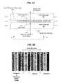
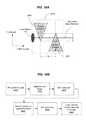
- FIG. 1shows an example scanning laser display system having a light-emitting screen made of laser-excitable light-emitting materials (e.g., phosphors) emitting colored lights under excitation of a scanning laser beam that carries the image information to be displayed.
- a light-emitting screenmade of laser-excitable light-emitting materials (e.g., phosphors) emitting colored lights under excitation of a scanning laser beam that carries the image information to be displayed.
- laser-excitable light-emitting materialse.g., phosphors
- FIGS. 2A and 2Bshow one example screen structure with parallel light-emitting stripes and the structure of color pixels on the screen in FIG. 1 .
- FIG. 3shows an example implementation of the laser display system in FIG. 1 in a pre-objective scanning configuration having multiple lasers that direct multiple laser beams on the screen.
- FIG. 4shows an example implementation of a post-objective scanning beam display system based on the laser display system in FIG. 1 .
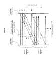
- FIG. 5shows one example for simultaneously scanning consecutive scan lines with multiple excitation laser beams and an invisible servo beam.
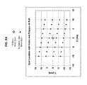
- FIG. 5Ashows a map of beam positions on the screen produced by a laser array of thirty-six excitation lasers and one IR servo laser when a vertical galvo scanner and a horizontal polygon scanner are at their respective null positions.
- FIG. 6shows one example of a scanning display system using a servo feedback control based on a scanning servo beam.
- FIG. 7shows an example of a servo detector for detecting the servo feedback light in FIG. 6 .
- FIGS. 8 and 9show two screen examples for the servo control based on a scanning servo beam.
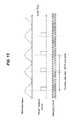
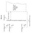
- FIG. 10shows optical power of servo light having optical signals corresponding to stripe dividers on the screen.
- FIG. 11shows an example of a screen having peripheral reference mark regions that include servo reference marks that produce feedback light for various servo control functions.
- FIG. 12shows a start of line reference mark in a peripheral reference mark region to provide a reference for the beginning of the active fluorescent area on the screen.
- FIGS. 13 and 14show optical power of servo light having optical signals corresponding to stripe dividers, the start of line reference mark and end of line reference mark on the screen
- FIGS. 15 , 16 and 17show examples of a use of a sampling clock signal to measure position data of stripe dividers on the screen using servo feedback light from the excitation beam or the servo beam.
- FIG. 18Ashows an example of a vertical beam position reference mark for the screen in FIG. 11 .
- FIGS. 18B and 18Cshow a servo feedback control circuit and its operation in using the vertical beam position reference mark in FIG. 18A to control the vertical beam position on the screen.
- FIG. 19shows an example of the screen in FIG. 11 having the start of line reference mark and the vertical beam position reference marks.
- FIG. 20shows an operation of the servo control based on the servo beam that is scanned with the excitation beam.
- FIGS. 21 , 22 and 23show examples of screen designs that have IR servo feedback marks that do not affect the transmission amount of excitation beams while having a property of diffuse or specular reflection for at least the servo beams.
- FIG. 24shows an example of the screen design to have specularly reflective IR feedback marks and diffusively reflective areas outside the IR feedback marks on the screen.
- FIG. 25shows an example of a system based on the design in FIG. 24 .
- FIG. 26shows an example of a system that combines IR servo feedback and visible light servo feedback.
- FIGS. 27 , 28 , 29 and 30illustrate aspects of the system in FIG. 26 .
- FIG. 31shows a system implementation of the system in FIG. 26 .
- Examples of scanning beam display systems in this applicationuse screens with light-emitting materials or fluorescent materials to emit light under optical excitation to produce images, including laser video display systems.
- Various examples of screen designs with light-emitting or fluorescent materialscan be used.
- three different color phosphors that are optically excitable by the laser beam to respectively produce light in red, green, and blue colors suitable for forming color imagesmay be formed on the screen as pixel dots or repetitive red, green and blue phosphor stripes in parallel.
- Phosphor materialsare one type of fluorescent materials.
- Various described systems, devices and features in the examples that use phosphors as the fluorescent materialsare applicable to displays with screens made of other optically excitable, light-emitting, non-phosphor fluorescent materials.
- quantum dot materialsemit light under proper optical excitation and thus can be used as the fluorescent materials for systems and devices in this application.
- semiconductor compoundssuch as, among others, CdSe and PbS, can be fabricated in form of particles with a diameter on the order of the exciton Bohr radius of the compounds as quantum dot materials to emit light.
- different quantum dot materials with different energy band gap structuresmay be used to emit different colors under the same excitation light.
- Quantum dotsare between 2 and 10 nanometers in size and include approximately tens of atoms such between 10 to 50 atoms.
- Quantum dotsmay be dispersed and mixed in various materials to form liquid solutions, powders, jelly-like matrix materials and solids (e.g., solid solutions).
- Quantum dot films or film stripesmay be formed on a substrate as a screen for a system or device in this application.
- three different quantum dot materialscan be designed and engineered to be optically excited by the scanning laser beam as the optical pump to produce light in red, green, and blue colors suitable for forming color images.
- Such quantum dotsmay be formed on the screen as pixel dots arranged in parallel lines (e.g., repetitive sequential red pixel dot line, green pixel dot line and blue pixel dot line).
- Examples of scanning beam display systems described hereuse at least one scanning laser beam to excite color light-emitting materials deposited on a screen to produce color images.
- the scanning laser beamis modulated to carry images in red, green and blue colors or in other visible colors and is controlled in such a way that the laser beam excites the color light-emitting materials in red, green and blue colors with images in red, green and blue colors, respectively.
- the scanning laser beamcarries the images but does not directly produce the visible light seen by a viewer. Instead, the color light-emitting fluorescent materials on the screen absorb the energy of the scanning laser beam and emit visible light in red, green and blue or other colors to generate actual color images seen by the viewer.
- Laser excitation of the fluorescent materials using one or more laser beams with energy sufficient to cause the fluorescent materials to emit light or to luminesceis one of various forms of optical excitation.
- the optical excitationmay be generated by a non-laser light source that is sufficiently energetic to excite the fluorescent materials used in the screen.
- non-laser excitation light sourcesinclude various light-emitting diodes (LEDs), light lamps and other light sources that produce light at a wavelength or a spectral band to excite a fluorescent material that converts the light of a higher energy into light of lower energy in the visible range.
- the excitation optical beam that excites a fluorescent material on the screencan be at a frequency or in a spectral range that is higher in frequency than the frequency of the emitted visible light by the fluorescent material. Accordingly, the excitation optical beam may be in the violet spectral range and the ultra violet (UV) spectral range, e.g., wavelengths under 420 nm.
- UVultra violet
- Violet or a UV laser beamis used as an example of the excitation light for a phosphor material or other fluorescent material and may be light at other wavelength.
- FIG. 1illustrates an example of a laser-based display system using a screen having color phosphor stripes.
- color pixilated light-emitting areasmay also be used to define the image pixels on the screen.
- the systemincludes a laser module 110 to produce and project at least one scanning laser beam 120 onto a screen 101 .
- the screen 101has parallel color phosphor stripes in the vertical direction and two adjacent phosphor stripes are made of different phosphor materials that emit light in different colors.
- red phosphorabsorbs the laser light to emit light in red
- green phosphorabsorbs the laser light to emit light in green
- blue phosphorabsorbs the laser light to emit light in blue.
- Adjacent three color phosphor stripesare in three different colors.
- the laser beam 120is at the wavelength within the optical absorption bandwidth of the color phosphors and is usually at a wavelength shorter than the visible blue and the green and red colors for the color images.
- the color phosphorsmay be phosphors that absorb UV light in the spectral range below 420 nm to produce desired red, green and blue light.
- the laser module 110can include one or more lasers such as UV diode lasers to produce the beam 120 , a beam scanning mechanism to scan the beam 120 horizontally and vertically to render one image frame at a time on the screen 101 , and a signal modulation mechanism to modulate the beam 120 to carry the information for image channels for red, green and blue colors.
- laserssuch as UV diode lasers to produce the beam 120
- a beam scanning mechanismto scan the beam 120 horizontally and vertically to render one image frame at a time on the screen 101
- a signal modulation mechanismto modulate the beam 120 to carry the information for image channels for red, green and blue colors.
- Such display systemsmay be configured as rear scanning systems where the viewer and the laser module 110 are on the opposite sides of the screen 101 .
- such display systemsmay be configured as front scanning systems where the viewer and laser module 110 are on the same side of the screen 101 .
- FIG. 2Ashows an exemplary design of the screen 101 in FIG. 1 .
- the screen 101may include a rear substrate 201 which is transparent to the scanning laser beam 120 and faces the laser module 110 to receive the scanning laser beam 120 .
- a second front substrate 202is fixed relative to the rear substrate 201 and faces the viewer in a rear scanning configuration.
- a color phosphor stripe layer 203is placed between the substrates 201 and 202 and includes phosphor stripes.
- the color phosphor stripes for emitting red, green and blue colorsare represented by “R”, “G” and “B,” respectively.
- the front substrate 202is transparent to the red, green and blue colors emitted by the phosphor stripes.
- the substrates 201 and 202may be made of various materials, including glass or plastic panels.
- the rear substrate 201can be a thin film layer and is configured to recycle the visible energy toward the viewer.
- Each color pixelincludes portions of three adjacent color phosphor stripes in the horizontal direction and its vertical dimension is defined by the beam spread of the laser beam 120 in the vertical direction. As such, each color pixel includes three subpixels of three different colors (e.g., the red, green and blue).
- the laser module 110scans the laser beam 120 one horizontal line at a time, e.g., from left to right and from top to bottom to fill the screen 101 .
- the relative alignment of the laser module 110 and the screen 101can be monitored and controlled to ensure proper alignment between the laser beam 120 and each pixel position on the screen 101 .
- the laser module 110can be controlled to be fixed in position relative to the screen 101 so that the scanning of the beam 120 can be controlled in a predetermined manner to ensure proper alignment between the laser beam 120 and each pixel position on the screen 101 .
- the scanning laser beam 120is directed at the green phosphor stripe within a pixel to produce green light for that pixel.
- FIG. 2Bfurther shows the operation of the screen 101 in a view along the direction B-B perpendicular to the surface of the screen 101 . Since each color stripe is longitudinal in shape, the cross section of the beam 120 may be shaped to be elongated along the direction of the stripe to maximize the fill factor of the beam within each color stripe for a pixel. This may be achieved by using a beam shaping optical element in the laser module 110 .
- a laser source that is used to produce a scanning laser beam that excites a phosphor material on the screenmay be a single mode laser or a multimode laser.
- the lasermay also be a single mode along the direction perpendicular to the elongated direction phosphor stripes to have a beam spread that is confined by and is smaller than the width of each phosphor stripe.
- this laser beammay have multiple modes to spread over a larger area than the beam spread in the direction across the phosphor stripe.
- a laser array 310 with multiple lasersis used to generate multiple laser beams 312 to simultaneously scan the screen 101 for enhanced display brightness.
- a signal modulation controller 320is provided to control and modulate the lasers in the laser array 310 so that the laser beams 312 are modulated to carry the image to be displayed on the screen 101 .
- the signal modulation controller 320can include a digital image processor that generates digital image signals for the three different color channels and laser driver circuits that produce laser control signals carrying the digital image signals.
- the laser control signalsare then applied to modulate the lasers, e.g., the currents for laser diodes, in the laser array 310 .
- the beam scanningcan be achieved by using a scanning mirror 340 such as a galvo mirror for the vertical scanning and a multi-facet polygon scanner 350 for the horizontal scanning.
- a scan lens 360can be used to project the scanning beams form the polygon scanner 350 onto the screen 101 .
- the scan lens 360is designed to image each laser in the laser array 310 onto the screen 101 .
- Each of the different reflective facets of the polygon scanner 350simultaneously scans N horizontal lines where N is the number of lasers.
- the laser beamsare first directed to the galvo mirror 340 and then from the galvo mirror 340 to the polygon scanner 350 .
- the output scanning beams 120are then projected onto the screen 101 .
- a relay optics module 330is placed in the optical path of the laser beams 312 to modify the spatial property of the laser beams 312 and to produce a closely packed bundle of beams 332 for scanning by the galvo mirror 340 and the polygon scanner 350 as the scanning beams 120 projected onto the screen 101 to excite the phosphors and to generate the images by colored light emitted by the phosphors.
- a relay optics module 370is inserted between the scanners 340 and 350 to image the reflective surface of the reflector in the vertical scanner 340 into a respective reflecting facet of the polygon scanner 350 in order to prevent beam walk across the thin facet of the polygon scanner 350 in the vertical direction.
- the laser beams 120are scanned spatially across the screen 101 to hit different color pixels at different times. Accordingly, each of the modulated beams 120 carries the image signals for the red, green and blue colors for each pixel at different times and for different pixels at different times. Hence, the beams 120 are coded with image information for different pixels at different times by the signal modulation controller 320 .
- the beam scanningthus maps the time-domain coded image signals in the beams 120 onto the spatial pixels on the screen 101 .
- the modulated laser beams 120can have each color pixel time equally divided into three sequential time slots for the three color subpixels for the three different color channels.
- the modulation of the beams 120may use pulse modulation techniques to produce desired grey scales in each color, a proper color combination in each pixel, and desired image brightness.
- the multiple beams 120are directed onto the screen 101 at different and adjacent vertical positions with two adjacent beams being spaced from each other on the screen 101 by one horizontal line of the screen 101 along the vertical direction.
- the beams 120may not be aligned with each other along the vertical direction on the screen 101 and may be at different positions on the screen 101 along the horizontal direction.
- the beams 120can only cover one portion of the screen 101 .
- the spinning of the polygon scanner 350causes the beams 120 from N lasers in the laser array 310 to scan one screen segment of N adjacent horizontal lines on the screen 101 .
- the galvo mirror 340tilts linearly to change its tiling angle at a given rate along a vertical direction from the top towards the bottom during the scanning by the polygon until the entire screen 101 is scanned to produce a full screen display.
- the galvoretraces to its top position and the cycle is repeated in synchronization with the refresh rate of the display.
- the beams 120may not be aligned with each other along the vertical direction on the screen 101 and may be at different positions on the screen 101 along the horizontal direction.
- the beams 120can only cover one portion of the screen 101 .
- the spinning of the polygon scanner 350causes the beams 120 from N lasers in the laser array 310 to scan one screen segment of N adjacent horizontal lines on the screen 101 .
- the galvo mirror 340is adjusted to a different fixed angular position so that the vertical positions of all N beams 120 are adjusted to scan the next adjacent screen segment of N horizontal lines. This process iterates until the entire screen 101 is scanned to produce a full screen display.
- the scan lens 360is located downstream from the beam scanning devices 340 and 350 and focuses the one or more scanning excitation beams 120 onto the screen 101 .
- This optical configurationis referred to as a “pre-objective” scanning system.
- a scanning beam directed into the scan lens 360is scanned along two orthogonal directions. Therefore, the scan lens 360 is designed to focus the scanning beam onto the screen 101 along two orthogonal directions.
- the scan lens 360can be complex and, often, are made of multiples lens elements.
- the scan lens 360can be a two-dimensional f-theta lens that is designed to have a linear relation between the location of the focal spot on the screen and the input scan angle (theta) when the input beam is scanned around each of two orthogonal axes perpendicular to the optic axis of the scan lens.
- the two-dimensional scan lens 360such as a f-theta lens in the pre-objective configuration can exhibit optical distortions along the two orthogonal scanning directions which cause beam positions on the screen 101 to trace a curved line.
- the scan lens 360can be designed with multiple lens elements to reduce the bow distortions and can be expensive to fabricate.
- a post-objective scanning beam display systemcan be implemented to replace the two-dimensional scan lens 360 with a simpler, less expensive 1-dimensional scan lens.
- U.S. patent application Ser. No. 11/742,014 entitled “POST-OBJECTIVE SCANNING BEAM SYSTEMS” and filed on Apr. 30, 2007(U.S. Patent Publication No. 2008/0247024) describes examples of post-objective scanning beam systems suitable for use with phosphor screens described in this application and is incorporated by reference as part of the specification of this application.
- FIG. 4shows an example implementation of a post-objective scanning beam display system based on the system design in FIG. 1 .
- a laser array 310 with multiple lasersis used to generate multiple laser beams 312 to simultaneously scan a screen 101 for enhanced display brightness.
- a signal modulation controller 320is provided to control and modulate the lasers in the laser array 310 so that the laser beams 312 are modulated to carry the image to be displayed on the screen 101 .
- the beam scanningis based on a two-scanner design with a horizontal scanner such as a polygon scanner 350 and a vertical scanner such as a galvanometer scanner 340 . Each of the different reflective facets of the polygon scanner 350 simultaneously scans N horizontal lines where N is the number of lasers.
- a relay optics module 330reduces the spacing of laser beams 312 to form a compact set of laser beams 332 that spread within the facet dimension of the polygon scanner 350 for the horizontal scanning.
- Downstream from the polygon scanner 350there is a 1-D horizontal scan lens 380 followed by a vertical scanner 340 (e.g., a galvo mirror) that receives each horizontally scanned beam 332 from the polygon scanner 350 through the 1-D scan lens 380 and provides the vertical scan on each horizontally scanned beam 332 at the end of each horizontal scan prior to the next horizontal scan by the next facet of the polygon scanner 350 .
- the vertical scanner 340directs the 2-D scanning beams 390 to the screen 101 .
- the 1-D scan lens 380is placed downstream from the polygon scanner 140 and upstream from the vertical scanner 340 to focus each horizontal scanned beam on the screen 101 and minimizes the horizontal bow distortion to displayed images on the screen 101 within an acceptable range, thus producing a visually “straight” horizontal scan line on the screen 101 .
- Such a 1-D scan lens 380 capable of producing a straight horizontal scan lineis relatively simpler and less expensive than a 2-D scan lens of similar performance.
- the vertical scanner 340Downstream from the scan lens 380 , is a flat reflector and simply reflects the beam to the screen 101 and scans vertically to place each horizontally scanned beam at different vertical positions on the screen 101 for scanning different horizontal lines.
- the dimension of the reflector on the vertical scanner 340 along the horizontal directionis sufficiently large to cover the spatial extent of each scanning beam coming from the polygon scanner 350 and the scan lens 380 .
- the system in FIG. 4is a post-objective design because the 1-D scan lens 380 is upstream from the vertical scanner 340 . In this particular example, there is no lens or other focusing element downstream from the vertical scanner 340 .
- the distance from the scan lens to a location on the screen 101 for a particular beamvaries with the vertical scanning position of the vertical scanner 340 . Therefore, when the 1-D scan lens 380 is designed to have a fixed focal distance along the straight horizontal line across the center of the elongated 1-D scan lens, the focal properties of each beam must change with the vertical scanning position of the vertical scanner 380 to maintain consistent beam focusing on the screen 101 .
- a dynamic focusing mechanismcan be implemented to adjust convergence of the beam going into the 1-D scan lens 380 based on the vertical scanning position of the vertical scanner 340 .
- a stationary lens and a dynamic refocus lenscan be used as the dynamic focusing mechanism.
- Each beamis focused by the dynamic focus lens at a location upstream from the stationary lens.
- the output light from the lensis collimated.
- the output light from the collimator lens toward the polygon scanner 350can be either divergent or convergent.
- a refocusing lens actuatorcan be used to adjust the relative position between the lenses in response to a control signal.
- the refocusing lens actuatoris used to adjust the convergence of the beam directed into the 1-D scan lens 380 along the optical path from the polygon scanner 350 in synchronization with the vertical scanning of the vertical scanner 340 .
- the vertical scanner 340 in FIG. 4scans at a much smaller rate than the scan rate of the first horizontal scanner 350 and thus a focusing variation caused by the vertical scanning on the screen 101 varies with time at the slower vertical scanning rate. This allows a focusing adjustment mechanism to be implemented in the system of FIG. 1 with the lower limit of a response speed at the slower vertical scanning rate rather than the high horizontal scanning rate.
- the beams 120 on the screen 101are located at different and adjacent vertical positions with two adjacent beams being spaced from each other on the screen 101 by one horizontal line of the screen 101 along the vertical direction.
- the beams 120may not be aligned with each other along the vertical direction on the screen 101 and may be at different positions on the screen 101 along the horizontal direction.
- the beams 120can cover one portion of the screen 101 .
- FIG. 5illustrates the above simultaneous scanning of one screen segment with multiple scanning laser beams 120 at a time.
- the beams 120behaves like a paint brush to “paint” one thick horizontal stroke across the screen 101 at a time to cover one screen segment between the start edge and the end edge of the image area of the screen 101 and then subsequently to “paint” another thick horizontal stroke to cover an adjacent vertically shifted screen segment.
- this configurationin an effect divides the screen 101 along the vertical direction into multiple screen segments so that the N scanning beams scan one screen segment at a time with each scanning beam scanning only one line in the screen segment and different beams scanning different sequential lines in that screen segment. After one screen segment is scanned, the N scanning beams are moved at the same time to scan the next adjacent screen segment.
- each scanning laser beam 120scans only a number of lines across the entire screen along the vertical direction that is equal to the number of screen segments.
- the polygon scanner 550 for the horizontal scanningcan operate at slower speeds than scanning speeds required for a single beam design where the single beam scans every line of the entire screen.
- the number of screen segmentsdecreases as the number of the lasers increases.
- the galvo mirror and the polygon scannerscan 30 lines per frame while a total of 108 lines per frame are scanned when there are only 10 lasers. Therefore, the use of the multiple lasers can increase the image brightness which is approximately proportional to the number of lasers used, and, at the same time, can also advantageously reduce the speed of the scanning system.
- a scanning display system described in this specificationcan be calibrated during the manufacture process so that the laser beam on-off timing and position of the laser beam relative to the fluorescent stripes in the screen 101 are known and are controlled within a permissible tolerance margin in order for the system to properly operate with specified image quality.
- the screen 101 and components in the laser module 101 of the systemcan change over time due to various factors, such as scanning device jitter, changes in temperature or humidity, changes in orientation of the system relative to gravity, settling due to vibration, aging and others.
- Such changescan affect the positioning of the laser source relative to the screen 101 over time and thus the factory-set alignment can be altered due to such changes.
- such changescan produce visible and, often undesirable, effects on the displayed images.
- a laser pulse in the scanning excitation beam 120may hit a subpixel that is adjacent to an intended target subpixel for that laser pulse due to a misalignment of the scanning beam 120 relative to the screen along the horizontal scanning direction.
- the coloring of the displayed imageis changed from the intended coloring of the image.
- a red pixel in the intended imagemay be displayed as a green pixel on the screen.
- a laser pulse in the scanning excitation beam 120may hit both the intended target subpixel and an adjacent subpixel next to the intended target subpixel due to a misalignment of the scanning beam 120 relative to the screen along the horizontal scanning direction. When this occurs, the coloring of the displayed image is changed from the intended coloring of the image and the image resolution deteriorates.
- Implementations of various alignment mechanismsare provided in this specification to maintain proper alignment of the scanning beam 120 on the desired sub-pixel to achieved desired image quality.
- These alignment mechanismsinclude reference marks on the screen, both in the fluorescent area and in one or more peripheral area outside the fluorescent area, emitted visible light in red, green and blue colors by the phosphor stripes to provide feedback light that is caused by the excitation beam 120 and represents the position and other properties of the scanning beam on the screen.
- the feedback lightcan be measured by using one or more optical servo sensors to produce one or more feedback servo signals and such feedback servo signals are used to generate a location map for red, green and blue sub-pixels on the screen.
- a servo control in the laser module 110processes this feedback servo signal to extract the information on the beam positioning and other properties of the beam on the screen and, in response, adjust the direction and other properties of the scanning beam 120 to ensure the proper operation of the display system.
- a feedback servo control systemcan be provided to use peripheral servo reference marks positioned outside the display area unobservable by the viewer to provide control over various beam properties, such as the horizontal positioning along the horizontal scanning direction perpendicular to the fluorescent stripes, the vertical positioning along the longitudinal direction of the fluorescent stripes, the beam focusing on the screen for control of image color (e.g., color saturation) and image sharpness, and the beam power on the screen for control of image brightness and uniformity of the image brightness across the screen.
- a screen calibration procedurecan be performed at the startup of the display system to measure the beam position information as a calibration map so having the exact positions of sub-pixels on the screen in the time domain.
- This calibration mapis then used by the laser module 110 to control the timing and positioning of the scanning beam 120 to achieve the desired color purity.
- a dynamic servo control systemcan be provided to regularly update the calibration map during the normal operation of the display system by using servo reference marks in the fluorescent area of the screen to provide the feedback light without affecting the viewing experience of a viewer. Examples for using servo light produced by phosphor stripe dividers from the excitation light and feedback light from other reference marks for servo control and screen calibration are described in the incorporated-by-reference PCT Patent Application No. PCT/US2007/004004 entitled “Servo-Assisted Scanning Beam Display Systems Using Fluorescent Screens” (PCT Publication No. WO 2007/095329).
- the display systems in this applicationprovide servo control mechanisms based on a designated servo beam that is scanned over the screen by the same scanning module that scans the image-carrying excitation optical beam.
- This designated servo beamis used to provide servo feedback control over the scanning excitation beam to ensure proper optical alignment and accurate delivery of optical pulses in the excitation beam during normal display operation.
- This designated servo beamhas an optical wavelength different from that of the excitation beam.
- this designated servo beamcan be an IR servo beam that may be invisible to human.
- the examples belowuse an IR servo beam 130 to illustrate features and operations of this designated servo beam.
- the laser module 110produces an invisible servo beam 130 such as an IR beam as an example of the designated servo beam.
- the laser module 110scans the servo beam 130 on to the screen 101 along with the excitation beam 120 . Different from the excitation beam 120 , the servo beam 130 is not modulated to carry image data.
- the servo beam 130can be a CW beam.
- the stripe dividers on the screen 101can be made reflective to the light of the servo beam 130 and to produce feedback light 132 by reflection.
- the servo beam 130has a known spatial relation with the excitation beam 120 . Therefore, the positioning of the servo beam 130 can be used to determine the positioning of the excitation beam 120 .
- This relationship between the servo beam 130 and the excitation beam 120can be determined by using reference servo marks such as a start of line (SOL) mark in a non-viewing area of the screen 101 .
- the laser module 101receives and detects the feedback light 132 to obtain positioning information of the servo beam 130 on the screen 101 and uses this positioning information to control alignment of the excitation beam 120 on the screen.
- the servo beam 130is invisible to human and thus does not produce any noticeable visual artifact on the screen 101 during the normal operation of the system when images are produced on the screen 101 .
- the servo beam 130can have a wavelength in a range from 780 nm to 820 nm.
- the screen 101can be made to have a filter that blocks the invisible servo beam 130 from exiting the screen 101 on the viewer side.
- a cutoff absorbing filter with a bandpass transmission range only in the visible spectral rangee.g., from 420 nm to 680 nm
- the servo control of the excitation beam 120 based on the servo beam 130can be performed dynamically during the normal operation of the system. This servo design avoids manipulation of the image-producing excitation beam 120 during the normal display mode for servo operations and thus avoids any visual artifacts that may be caused by the servo-related manipulation of the image-producing excitation beam 120 .
- the scattered or reflected excitation light by the screen 101may also be used for servo control operations during a period when the system does not show images, e.g., during the startup period of the system or when the excitation beam 120 is outside the active display area of the screen 101 .
- the scattered or reflected excitation lightlabeled as light 122
- the servo beam 130is directed along with the one or more excitation beams 120 through the same optical path that includes the relay optics module 330 A or 330 B, the beam scanners 340 and 350 , and the scan lens 360 or 380 .
- the servo beam 130is scanned along with the scanning excitation beams 120 one screen segment at a time along the vertical direction of the screen.
- the servo beam 130is invisible and can be overlapped with a scanning path of one excitation beam 120 or along its own scanning path that is different from a path of any of the excitation beams 120 .
- the spatial relation between the servo beam 130 and each excitation beam 120is known and fixed so that the positioning of the servo beam 130 on the screen 101 can be used to infer positioning of each excitation beam 120 .
- a light source for generating the servo beam 130 and a light source for generating an excitation beam 120can be semiconductor lasers in a light source module which can be an array of lasers and at least one of the lasers in the laser array can be a servo laser that produces the servo beam 130 .
- the location of the servo laseris known relative to each excitation laser in the laser array in the laser module 110 .
- the servo beam 130 and each excitation beam 120are directed through the same relay optics, the same beam scanners and the same projection lens and are projected on the screen 101 . Therefore, the positioning of the servo beam 130 on the screen 101 has a known relation with the positioning of each excitation beam 120 on the screen.
- This relation between the servo beam 130 and each excitation beam 120can be used to control the excitation beam 120 based on measured positioning of the servo beam 130 .
- the relative position relation between the servo beam 130 and each excitation beam 120can be measured using the servo feedback, e.g., during a calibration process that may be separately performed or performed during the power-up period of the system. The measured relative position relation is used for the servo feedback control.
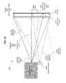
- FIG. 5Ashows a map of beam positions on the screen produced by a laser array of thirty-six excitation lasers and one IR servo laser when a vertical galvo scanner and a horizontal polygon scanner are at their respective null positions in a prototype pre-objective scanning display system.
- the thirty-six excitation lasersare arranged in a 4 ⁇ 9 laser array and the IR servo laser is placed in the center of the laser array.
- the laser beamsoccupy an area of about 20 mm ⁇ 25 mm on the screen.
- the vertical spacingis one half of a pixel between two vertically adjacent excitation lasers and the horizontal spacing between two adjacent excitation lasers is 3.54 pixels.
- each scan in one screen segmentproduces thirty-six horizontal lines on the screen occupying thirty-six pixels along the vertical direction.
- these thirty-seven laser beamsare scanned together based on the scanning shown in FIG. 5 to scan one screen segment at a time to sequentially scan different screen segments at different vertical positions to scan the entire screen.
- the IR servo laseris fixed in position with respect to each and every one of the thirty-six excitation lasers, the positioning of the servo beam 130 produced by the IR servo laser on the screen 101 has a known relation with respect to each beam spot of an excitation beam 120 from each of the thirty-six excitation lasers.
- FIG. 6illustrates a scanning beam display system based on a servo control using the invisible servo beam 130 .
- a display processor and controller 640can be used to provide control functions and control intelligence based on servo detector signals from radiation servo detectors 620 that detect servo feedback light 132 from the screen 101 .
- a single detector 620may be sufficient and two or more servo detectors 620 can be used to improve the servo detection sensitivity.
- one or more radiation servo detectors 630may also be used to collect excitation servo light 122 produced by scattering or reflecting the excitation beam 120 at the screen to provide additional feedback signals to the processor and controller 640 for the servo control.
- This use of the servo light 122 for feedback controlcan be an optional feature that is used in combination with the IR servo feedback control.
- the IR servo feedback alone without the feedback based on the feedback light 122 shown in FIG. 6can be sufficient to align the excitation beam 120 to the proper phosphor stripes on the screen 101 . Examples for using the servo light 122 produced by phosphor stripe dividers for servo control are described in the incorporated-by-reference PCT Patent Application No. PCT/US2007/004004 entitled “Servo-Assisted Scanning Beam Display Systems Using Fluorescent Screens” (PCT Publication No. WO 2007/095329).
- a scanning projection module 610is provided to scan and project the excitation and servo beams 120 and 130 onto the screen 101 .
- the module 610can be in a post-objective configuration or a pre-objective configuration.
- the image datais fed to the display processor and controller 640 which produces an image data signal carrying the image data to the signal modulator controller 520 for the excitation lasers 510 .
- the servo laserwhich is among the excitation lasers in the array 510 is not modulated to carry image data.
- the signal modulation controller 520can include laser driver circuits that produce laser modulation signals carrying image signals with image data assigned to different lasers 510 , respectively.
- the laser control signalsare then applied to modulate the lasers in the laser array 510 , e.g., the currents for laser diodes to produce the laser beams 512 .
- the display processor and controller 640also produces laser control signals to the lasers in the laser array 510 to adjust the laser orientation to change the vertical beam position on the screen 101 or the DC power level of each laser.
- the display processor and controller 5930further produces scanning control signals to the scanning projection module 610 to control and synchronize the horizontal polygon scanner and the vertical scanner.
- FIG. 7shows one example of the servo detector design where a servo detector 620 detects the servo feedback light 132 .
- the servo detector 620can be a detector designed to be sensitive to light of the servo beam wavelength for the invisible servo beam 130 and less sensitive to other light such as the visible light and the excitation light.
- An optical filter 710can be used to filter the light from the screen 101 to selectively transmit the servo feedback light 132 while blocking light at other wavelengths, such as the excitation light and visible light. Such a filter allows a wider range of optical detectors to be used as the servo detector.
- FIG. 7also shows an example of an optional servo detector 630 for detecting the servo feedback light 122 at the excitation wavelength.
- the servo detector 620can be a detector designed to be sensitive to light of the excitation wavelength of the excitation beam 120 and less sensitive to light at wavelengths of the servo beam 130 and the visible light emitted by the screen 101 .
- An optical filter 720can be used to filter the light from the screen 101 to selectively transmit the excitation servo feedback light 122 while blocking light at other wavelengths.
- the servo detector signals 721 and 722 from the servo detectors 620 and 630are directed to the processor and controller 640 for servo control operations.
- FIGS. 8 and 9show two exemplary screen designs for the screen 101 for providing the feedback light 122 and 132 .
- each strip divider 810is made optically reflective to the servo and excitation beams so the reflection can be used as the feedback light 132 .
- the strip divider 810can also be made reflective and opaque to light to optically isolate adjacent light-emitting stripes to enhance contrast and to reduce cross talk.
- the light-emitting stripessuch phosphor stripes emitting red, green and blue light are less reflective to the servo and excitation beams than the stripe dividers 810 so that the feedback light 132 exhibits a spike every time the servo or excitation beams 130 pass through a stripe divider 810 .
- FIG. 9shows another screen design where a reflective servo reference mark 910 is formed on the excitation side of each strip divider 901 , e.g., a reflective stripe coating.
- the beam 120 or 130scans across the light-emitting stripes and the reflections produced by the stripe dividers can be used to indicate horizontal positions of the stripe dividers, spacing between two adjacent stripe dividers and horizontal positions of the horizontally scanned beam 120 or 130 . Therefore, reflections from the stripe dividers can be used for servo control of the horizontal alignment between the beam 120 and the light-emitting strips.
- FIG. 10shows operation of the stripe dividers as alignment reference marks.
- the servo beam 120 or 130is scanned horizontally across the screen 101 and the light at the servo beam shows a low power when the servo beam 130 is at a light-emitting stripe and a high power when the servo beam is at a stripe divider.
- the power of the servo lightshows a periodic pattern in each horizontal scan where the high power peak corresponds to a stripe divider. This pattern can be used to measure the position of the stripe dividers or the width of each stripe divider based on clock cycles of a clocking signal in the processor and controller 640 .
- This measured informationis used to update a positioning map of each excitation beam 120 in the horizontal scan.
- the beam spot of the servo beam 130is greater than one width of the subpixel but is less than one color pixel made up by three adjacent subpixels, the power of the servo light 132 still shows a periodic pattern in each horizontal scan where the high power peak corresponds to one color pixel and thus can be used for servo control.
- additional alignment reference markscan be implemented to determine the relative position of the beam and the screen and other parameters of the excitation beam on the screen. For example, during a horizontal scan of the excitation and servo beams across the light-emitting stripes, a start of line mark can be provided for the system to determine the beginning of the active light-emitting display area of the screen 101 so that the signal modulation controller of the system can properly control the timing in delivering optical pulses to targeted pixels. An end of line mark can also be provided for the system to determine the end of the active light-emitting display area of the screen 101 during a horizontal scan.
- a vertical alignment referenced markcan be provided for the system to determine whether the scanning beams are pointed to a proper vertical location on the screen.
- Other examples for reference marksmay be one or more reference marks for measuring the beam spot size on the screen and one or more reference marks on the screen to measure the optical power of the excitation beam 120 .
- Such reference markscan be placed a region outside the active fluorescent area of the screen 101 , e.g., in one or more peripheral regions of the active fluorescent screen area and are used for both excitation and servo beams.
- FIG. 11illustrates one example of a fluorescent screen 101 having peripheral reference mark regions.
- the screen 101includes a central active light-emitting display area 1100 with parallel fluorescent stripes for displaying images, two stripe peripheral reference mark regions 1110 and 1120 that are parallel to the fluorescent stripes.
- Each peripheral reference mark regioncan be used to provide various reference marks for the screen 101 .
- only the left peripheral reference mark region 1110is provided without the second region 1120 when the horizontal scan across the fluorescent stripes is directed from the left to the right of the area 1100 .
- Such a peripheral reference mark region on the screen 101allows the scanning display system to monitor certain operating parameters of the system.
- a reference mark in the peripheral reference mark regioncan be used for a servo control operation based on the servo feedback light 132 generated from the servo beam 130 .
- a reference mark in the peripheral reference mark regioncan be used for servo control operation based on the servo feedback light 122 .
- a reference mark in the peripheral reference mark regioncan be used to measure both the excitation beam 120 and the servo beam 130 for a servo control operation in some implementations. The description on various examples of reference marks below may specifically refer to the excitation beam 120 and similar functions can be used in connection with the servo beam 130 .
- each scancan include a continuous mode period when an excitation beam sans through the peripheral referenced mark region for the dynamic servo sensing and control and a display mode period when the modulation of the excitation beam is turned on to produce image-carrying optical pulses as the excitation beam scans through the active fluorescent display area 1100 .
- the servo beam 130is not modulated to carry image data and thus can be a continuous beam with a constant beam power when incident onto the screen 101 .
- the power of the reflected servo light in the feedback light 132is modulated by the reference marks and stripe dividers and other screen pattern on the screen 101 .
- the modulated power of the reflected servo lightcan be used to measure the location of the servo beam 130 on the screen 101 .
- FIG. 12shows an example of a start of line (SOL) reference mark 1210 in the left peripheral region 1110 in the screen 101 .
- the SOL reference mark 1210can be an optically reflective, diffusive or fluorescent stripe parallel to the fluorescent stripes in the active light-emitting region 1100 of the screen 101 .
- the SOL reference mark 1210is fixed at a position with a known distance from the first fluorescent stripe in the region 1100 .
- SOL patternsmay be a single reflective stripe in some implementations and may include multiple vertical lines with uniform or variable spacing in other implementations. Multiple lines are selected for redundancy, increasing the signal to noise ratio, accuracy of position (time) measurement, and providing missing pulse detection.
- the scanning excitation beam 120is scanned from the left to the right in the screen 101 by first scanning through the peripheral reference mark region 1110 and then through the active region 1100 .
- the signal modulation controller in the laser module 110 of the systemsets the beam 120 in a mode that ensures adequate sampling of information without crosstalk (e.g. one beam at a time during one frame)
- the scanning excitation beam 120scans through the SOL reference mark 1210
- the light reflected, scattered or emitted by the SOL reference mark 1210 due to the illumination by the excitation beam 1210can be measured at an SOL optical detector located near the SOL reference mark 1210 .
- the presence of this signalindicates the location of the beam 120 .
- the SOL optical detectorcan be fixed at a location in the region 1110 on the screen 101 or off the screen 101 . Therefore, the SOL reference mark 1210 can be used to allow for periodic alignment adjustment during the lifetime of the system.
- the lasercan be controlled to, after the delay representing the time for scanning the beam from the SOL 1210 to the left edge of the active display area 1100 , operate in the image mode and carry optical pulses with imaging data.
- the systemrecalls a previously measured value for the delay from SOL pulse to beginning of the image area 1100 .
- This processcan be implemented in each horizontal scan to ensure that each horizontal line starts the image area properly and optical pulses in each horizontal scan are aligned to the light-emitting stripes.
- the correctionis made prior to painting the image for that line in the area 1100 on the screen 101 , so there is no time lag in displaying the images caused by the servo control. This allows for both high frequency (up to line scan rate) and low frequency errors to be corrected.
- the servo beam 130can be used to provide a positioning reference for each excitation beam 120 for controlling both the timing for beginning image-carrying pulses before the excitation beam enters the active light-emitting area 1100 and during the normal display when the excitation beam 120 scans in the active light-emitting region 1100 .
- FIG. 13illustrates the detected signal power of the light at the servo beam wavelength in the feedback light 132 to show optical signals indicative of positions of the SOL mark and stripe dividers on the screen 101 .
- the optical peaks in the feedback light shown in FIGS. 13 and 14are idealized as sharp square wave signals and are likely to have tailing and leading profiles shown in FIGS. 15-16 .
- Such a pulse signal with trailing and leading profilescan be converted into square wave like pulse signals by edge detection.
- an end-of-line (EOL) reference markcan be implemented on the opposite side of the screen 101 , e.g., in the peripheral reference mark region 1120 in FIG. 11 .
- the SOL markis used to ensure the proper alignment of the laser beam with the beginning of the image area. This does not ensure the proper alignment during the entire horizontal scan because the position errors can be present across the screen.
- Implementing the EOL reference mark and an end-of-line optical detector in the region 1120can be used to provide a linear, two point correction of laser beam position across the image area.
- FIG. 14illustrates the detected signal power of the light at the servo beam wavelength in the feedback light 132 to show optical signals indicative of positions of the SOL mark, stripe dividers and EOL mark on the screen 101
- the laseris turned on continuously in a continuous wave (CW) mode prior to reaching the EOL sensor area.
- CWcontinuous wave
- the lasercan be returned to image mode and timing (or scan speed) correction calculations are made based on the time difference between the SOL and EOL pulses. These corrections are applied to the next one or more lines. Multiple lines of SOL to EOL time measurements can be averaged to reduce noise.
- the positioning of the servo beam 130 on the screen 101can be measured. Because the servo beam 130 has a fixed relation with each excitation beam 120 , which can be measured at the SOL reference mark or EOL reference mark, any error in the positioning of the servo beam 130 suggests a corresponding error in each excitation beam 120 . Therefore, the positioning information of the servo beam 130 can be used in the servo control to control the servo beam 130 and each excitation beam 120 to reduce an alignment error of the excitation beam.
- the present servo controloperates to place each optical pulse in the excitation beam 120 near or at the center of a target light-emitting stripe to excite the light-emitting material in that stripe without spilling over to an adjacent light-emitting stripe.
- the servo controlcan be designed to achieve such alignment control by controlling the timing of each optical pulse in order to place the pulse at a desired position on the screen 101 during a horizontal scan. Accordingly, the servo control, i.e., the processor and controller 640 , needs to “know” horizontal positions of the light-emitting stripes in each horizontal line before each horizontal scan in order to control the timing of optical pulses during the scan.
- This information on horizontal positions of the light-emitting stripes in each horizontal lineconstitutes a two-dimensional position “map” of the active display area or light-emitting area of the screen 101 of (x, y) coordinates where x is the horizontal position of each stripe divider (or equivalently, the horizontal position of the center of each stripe) and y is the vertical position or ID number of a horizontal scan.
- This position map of the screen 101can be measured at the factory and may change in time due to changes in the system components due to temperature, aging and other factors. For example, thermal expansion effects, and distortions in the optical imaging system will need corresponding adjustments in the precise timing to activate each color in a pixel.
- this position map of the screen 101can vary from one system to another due to the component and device tolerances during the manufacturing.
- the position map of the screen 101can be obtained using the feedback light 122 and 132 in a calibration scanning when the system is not in the normal display mode, e.g., during the start-up phase of the system.
- the servo feedback light 132can be used in real time video display to monitor and measure changes in an existing position map of the screen 101 when the system is operating in the normal display mode to produce images on the screen 101 .
- This mode of the servo controlis referred to as dynamic servo.
- the dynamic monitoring of the screen 101can be useful when the system operates for an extended period time without a downtime because the screen 101 may undergo changes that can lead to significant changes to the position map of the screen 101 that is updated during the start-up phase of the system.
- the position map of the screen 101can be stored in the memory of the laser module 110 and reused for an interval of time if the effects that are being compensated for do not change significantly.
- the display systemwhen the display system is turned on, the display system can be configured to, as a default, set the timing of the laser pulses of the scanning laser beam based on the data in the stored position map.
- the servo controlcan operate to provide the real-time monitoring using the servo feedback light 132 and to control the pulse timing during the operation.
- the display systemwhen the display system is turned on, can be configured to, as a default, to perform a calibration using the excitation beam 120 and the servo beam 130 to scan through the entire screen 101 .
- the measured position dataare used to update the position map of the screen 101 .
- the systemcan be switched into the normal display mode and, subsequently during the normal display operation, only the servo beam 130 is used to monitor the screen 101 and the data on the screen 101 obtained from the servo beam 130 can be used to dynamically update the position map and thus to control the timing of pulses in the beam 120 in each horizontal scan.
- the calibration of the position map of the screen 101can be obtained by operating each scanning beam 120 or 130 in a continuous wave (CW) mode for one frame during which the scanning laser beams 120 and 130 simultaneously scan through the entire screen, one segment at a time as shown in FIG. 5 , when multiple laser beams 120 are used. If a single laser is used to produce one excitation beam 120 , the single scanning beam 120 is set in the CW mode to scan the entire screen 101 , one line at a time, along with the servo beam 130 . The feedback light 122 and 132 from the servo reference marks on the stripe dividers is used to measure the laser position on the screen 101 by using the servo detectors 620 and 630 .
- CWcontinuous wave
- the servo detector signals from the servo detectors 620 and 630can be sent through an electronic “peak” detector that creates an electronic pulse whenever a servo signal is at its highest relative amplitude.
- the time between these pulsescan be measured by a sampling clock in a digital circuit or microcontroller that is used by the processor and controller 640 to process and generate an error signal for controlling timing of optical pulses in each excitation beam 120 in a horizontal scan.
- the time between two adjacent pulses from the electronic peak detectorcan be used to determine the spacing of the two locations that produce the two adjacent electronic pulses based on the scan speed of the scanning beam 120 or 130 on the screen 101 . This spacing can be used to determine the subpixel width and subpixel position.
- servo measurements and correctionsare based on relative time measurements.
- a correction valuecan be calculated and used for some number N of adjacent sub-pixels because changes usually do not occur with significant changes between adjacent sub-pixels.
- FIG. 15shows one example of the detected reflected feedback light as a function of the scan time for a portion of one horizontal scan, the respective output of the peak detector and the sampling clock signal.
- a nominal subpixel with a width corresponding to 9 clock cycles of the sampling clock and an adjacent short subpixel corresponding to 8 clock cyclesare illustrated. In some implementations, the width of a subpixel may correspond to 10-20 clock cycles.
- the clock cycle of the sampling clock signal of the digital circuit or microcontroller for the servo controldictates the spatial resolution of the error signal. As an example for techniques to improve this spatial resolution, averaging over many frames can be utilized to effectively increase the spatial resolution of the error signal.
- FIG. 16shows one example of the detected reflected feedback light as a function of the scan time for a portion of one horizontal scan, the respective output of the peak detector and the sampling clock signal where a nominal subpixel corresponding to a width of 9 clock cycles and an adjacent long subpixel a corresponding to a width of 10 clock cycles re illustrated.
- FIG. 17illustrates an example where a pulse is missing.
- a missing pulsecan be determined if a pulse is not sampled or detected within the nominal number of clock cycles for a subpixel within the maximum expected deviation from the nominal number of clocks for a subpixel. If a pulse is missed, the nominal value of clock cycles for a subpixel can be assumed for that missing sub-pixel and the next sub-pixel can contain the timing correction for both sub-pixels. The timing correction can be averaged over both sub-pixels to improve the detection accuracy. This method may be extended for any number of consecutive missed pulses.
- the above use of the sampling clock signal to measure the position map of the screen 101can be used with detection with the excitation servo feedback light 122 or the servo feedback light 132 from the screen 101 .
- the position data from the excitation servo feedback light 122can provide data for each and every subpixel of the screen 101 .
- the position data obtained from the servo beam 130 and its corresponding feedback light 132only covers one horizontal scan line per screen segment as shown in FIG. 5 .
- the position data measured from the servo beam 130 for one screen segmentcan be used as a representative scan for all horizontal lines in that screen segment is used to update position data for all lines in that screen segment.
- Two or more servo beams 130may be used to increase the number of lines measured in each screen segment.
- Vertical position of each lasercan be monitored and adjusted by using an actuator, a vertical scanner, an adjustable lens in the optical path of each laser beam or a combination of these and other mechanisms.
- Vertical reference markscan be provided on the screen to allow for a vertical servo feedback from the screen to the laser module.
- One or more reflective, fluorescent or transmissive vertical reference markscan be provided adjacent to the image area of the screen 101 to measure the vertical position of each excitation beam 120 . Referring to FIG. 11 , such vertical reference marks can be placed in a peripheral reference mark region.
- One or more vertical mark optical detectorscan be used to measure the reflected, fluorescent or transmitted light from a vertical reference mark when illuminated by the beam 120 or 130 . The output of each vertical mark optical detector is processed and the information on the beam vertical position is used to control an actuator to adjust the vertical beam position on the screen 101 .
- FIG. 18Ashows an example of a vertical reference mark 2810 .
- the mark 2810includes is a pair of identical triangle reference marks 2811 and 2812 that are separated and spaced from each other in both vertical and horizontal directions to maintain an overlap along the horizontal direction.
- Each triangle reference mark 2811 or 2812is oriented to create a variation in the area along the vertical direction so that the beam 120 partially overlaps with each mark when scanning through the mark along the horizontal direction.
- the overlapping area on the mark with the beam 120changes in size.
- the relative positions of the two marks 2811 and 2812defines a predetermined vertical beam position and the scanning beam along a horizontal line across this predetermined vertical position scans through the equal areas as indicated by the shadowed areas in the two marks 2811 and 2812 .
- the beam positionWhen the beam position is above this predetermined vertical beam position, the beam sees a bigger mark area in the first mark 2811 than the mark area in the second mark 2812 and this difference in the mark areas seen by the beam increases as the beam position moves further up along the vertical direction. Conversely, when the beam position is below this predetermined vertical beam position, the beam sees a bigger mark area in the second mark 2812 than the mark area in the first mark 2811 and this difference in the mark areas seen by the beam increases as the beam position moves further down along the vertical direction.
- the feedback light from each triangle markis integrated over the mark and the integrated signals of the two marks are compared to produce a differential signal.
- the sign of the differential signalindicated the direction of the offset from the predetermined vertical beam position and the magnitude of the differential signal indicates the amount of the offset.
- the excitation beamis at the proper vertical position when the integrated light from each triangle is equal, i.e., the differential signal is zero.
- FIG. 18Bshows a portion of the signal processing circuit as part of the vertical beam position servo feedback control in the laser module 110 for the vertical reference mark in FIG. 18A .
- a PIN diode preamplifier 2910receives and amplifies the differential signal for the two reflected signals from the two marks 2811 and 2812 and directs the amplified differential signal to an integrator 2920 .
- An analog-to-digital converter 2930is provided to convert the differential signal into a digital signal.
- a digital processor 2940processes the differential signal to determine the amount and direction of the adjustment in the vertical beam position and accordingly produces a vertical actuator control signal. This control signal is converted into an analog control signal by a digital to analog converter 2950 and is applied to a vertical actuator controller 2960 which adjusts the actuator.
- FIG. 18Cfurther shows generation of the differential signal by using a single optical detector.
- FIG. 19shows an example of the screen in FIG. 11 having the start of line (SOL) reference mark and the vertical beam position reference marks. Multiple vertical beam position reference marks can be placed at different vertical positions to provide vertical position sensing of the excitation beams 120 in all screen segments.
- the example in FIG. 19shows the SOL reference mark is located between the vertical beam position reference marks and the screen display area so that, in a horizontal scan beginning from the left to the right, the excitation beam 120 or the servo beam 130 hits the SOL reference mark after the vertical beam position reference marks.
- the SOL reference markis located between the vertical beam position reference marks and the screen display area to ensure that the excitation beam 120 or the servo beam 130 hits the SOL reference mark before the vertical beam position reference marks.
- multiple vertical beam position reference markscan be placed at different vertical positions, e.g., one vertical reference mark for the servo beam 130 to provide vertical position sensing of the servo beam 130 in each screen segment. These vertical reference marks are presented by the numeral “ 1910 ” in FIG. 19 .
- the combination of the SOL reference 1210 , the vertical reference marks 1910 and the periodic pattern in the strip structure of the light-emitting area 1110provides positioning information of the invisible servo beam 130 , positioning information of the excitation beams 120 and the horizontal parameters of the pixels on the screen 101 for servo control in a scanning display system.
- FIG. 20shows an example of the operation of a servo control using the servo beam 130 during the normal display mode when each excitation beam 120 is used for carrying optical pulses for producing images on the screen 101 and is not used for servo control.
- the servo beam 130is a CW beam and is scanned over one horizontal line per screen segment with the scanning modulated excitation Laser beams 120 .
- the servo feedback light 132is detected by the one or more servo detectors 620 to measure an alignment error of the servo beam 130 on the screen 101 during the normal display.
- the alignment of each excitation laser beam 120is adjusted based on the measured alignment error of the servo beam 130 to reduce the alignment error of the excitation laser beam 120 .
- the red, green and blue light emitted by the screen 101 or a portion of back-reflected excitation light of the scanning excitation beam 120can be used to provide a calibration mechanism to calibrate the measurements obtained via the servo beam 130 .
- the parallel phosphor stripes and the stripe dividers on the screen 101are used to produce back-reflected feedback light 132 by reflection of the servo beam 132 at the stripe dividers.
- the screen 101can be designed to include IR feedback marks that are configured to produce desired feedback light 132 .
- the IR feedback markscan be registered with a special spatial relationship with respect to the stripe dividers or the phosphor stripes, e.g., a servo feedback mark is aligned in position with a light-emitting stripe or a division (a divider) between two adjacent parallel light-emitting stripes in the screen.
- the IR feedback markshave a fixed and known spatial relationship with respect to the stripe dividers or the phosphor stripes so that there is a fixed and known mapping of the positions of the IR feedback marks and the positions of the phosphor stripes and stripe dividers.
- FIG. 21shows an example design for the light-emitting screen 101 that includes IR feedback marks on the excitation side of the phosphor layer.
- This screen 101includes a phosphor stripe layer 2110 with parallel phosphor stripes emitting red, green and blue light under excitation of the excitation beam 120 , a back panel 2112 on the excitation side of the phosphor layer 2110 facing the excitation beam 120 and the IR servo beam 130 , and a front panel 2111 on the viewer side of the phosphor layer 2110 .
- IR feedback marks 2120are formed on the back surface of the back panel to provide the IR feedback light 132 by reflecting or scattering the IR servo beam 130 .
- the IR feedback marks 2120may be placed at other positions and can be located on either the excitation side or the viewer side of the phosphor layer 2110 .
- the IR feedback marks 2120are designed to provide position registration of the servo beam 130 on the screen and can be implemented in various configurations.
- the IR feedback marks 2120can be periodic parallel stripes that are parallel to the parallel phosphor stripes in the phosphor layer 2110 .
- An IR feedback mark 2120can be placed at any position relative to a stripe divider or a phosphor stripe in the phosphor layer 2110 along the horizontal direction, including a position horizontally displaced from a stripe divider or the center of a phosphor stripe.
- the width of each of the IR feedback marks 2120can be equal to the width of the beam spot of the IR servo beam 130 on the screen 101 when the detection for the IR servo feedback light 132 is based on a peak detector.
- IR feedback marks 2120 with a width wider than the width of the beam spot of the IR servo beam 130 on the screen 101can be used if the detection for the IR servo feedback light 132 is based on the position of each IR feedback mark 2120 with respect to a position reference such as the SOL mark.
- the width of the IR feedback marks 2120may be less than the width of each phosphor stripe, e.g., one half of the width of a phosphor stripe.
- the spacing between two adjacent IR feedback marks 2120can be greater than the spacing between two adjacent phosphor stripes.
- the IR mark spacingcan be 25 mm and the phosphor stripe spacing can be 1.5 mm.
- the IR feedback marks 2120can be made to be optically different from the areas surrounding and between the IR feedback marks 2120 to allow for optical detection of the IR feedback marks 2120 to register the positions of the IR feedback marks 2120 on the screen while maintaining the substantially the same optical transmission for the excitation beam 120 as the areas surrounding and between the IR feedback marks 2120 . Therefore, the presence of the IR feedback marks 2120 does not optically interfere with the optical transmission of the excitation beam 120 by optically imprinting the shapes of the marks 2120 on the excitation beam 120 that reaches the phosphor layer of the screen 101 .
- the IR feedback marks 2120can be implemented in various configurations.
- each IR feedback mark 2120can be made to have a smooth surface facing the excitation side and optically specularly reflective to light and the areas surrounding and between the IR feedback marks 2120 are configured to exhibit optically diffused reflection which spreads in different directions.
- the specularly reflective IR feedback marks 2120 and the diffusively reflective areas surrounding and between the marks 2120have the same optical transmission characteristics.
- the IR feedback marks 2120can also be made diffusively reflective to light and the areas surrounding and between the marks 2120 are made specularly reflective.
- the IR feedback marks 2120can have a transmissivity or reflectivity at the wavelength of the excitation beam 120 that is significantly different from the wavelength of the servo beam and servo wavelengths.
- the IR feedback marks 2120can be configured to be optically transparent to light of the excitation beam 120 and optically reflective to light of the servo beam 130 so that the IR feedback marks 2120 are optically “invisible” to the excitation beam 120 and reflect the servo beam 130 to produce the IR servo feedback light 132 .
- FIGS. 22 and 23show examples of screen layout configurations with vertical reference marks 1910 for measuring the vertical positions of the IR servo beam 130 .
- the vertical reference marks 1910are located on the edge of the screen, preferable outside the main display area of the screen.
- the vertical reference marks 1910are placed at the edges and in the middle of the screen and may be made to have the same optical transmission characteristics for light of the excitation beam 120 .
- FIG. 24shows a specific example of a screen design with specularly reflective IR feedback marks and optically diffusive areas surrounding and between the IR feedback marks.
- an IR feedback markis formed by a film stripe that has a smooth surface to produce a specular reflection 2430 of the incident IR servo light 130 .
- the screen area between two IR feedback marksis formed by a film layer with a roughened surface that diffuses light in reflecting the incident IR servo light 130 to produce the diffused reflection 2440 that spreads in different directions forming a diffused reflection cone.
- the two regions 2410 and 2420have approximately the same optical transmission for light of the excitation beam 120 .
- the above screen design for IR servo feedbackcan use the different optical behaviors of the specular reflection and the diffusive reflection of the IR servo beam 130 from the screen in the optical far field from the screen to facilitate the servo detection as shown in the example in FIG. 25 .
- FIG. 25shows an exemplary scanning beam display system 2500 that provides an IR servo feedback based on the screen design in FIG. 24 .
- the laser module 110projects and scans both the IR servo beam 130 and the excitation beam 120 onto the screen 101 with IR feedback marks.
- the laser module 110has a symmetric optic axis 2501 around which the beam scanning is performed.
- the screen 101has a construction as shown in FIG. 21 or 22 based on the design in FIG. 24 .
- An optical telecentric lens 2510such as a Fresnel lens layer is provided in to couple the incident scanning beams 120 and 130 from the laser module 110 onto the screen 101 in a substantially normal incidence to the screen 101 .
- the telecentric lens 2510is configured to have its symmetric optic axis 2502 to be parallel to the optic axis 2501 of the laser module 110 with an offset 2503 . As illustrated, the Fresnel lens 2510 is placed in front of the back surface of the screen 101 with an air gap 2520 .
- the IR servo detectionis provided by using an IR servo detector 2530 located along an optical path of the returned specular reflection 2430 of the incident IR servo light 130 from the IR feedback marks on the screen 101 .
- the location of the IR servo detector 2530is determined by the offset 2503 for receiving the returned specular reflection 2430 of the incident IR servo light 130 from each IR feedback mark on the screen 101 .
- Returned IR light in a direction different from the specular reflection direction at each IR feedback markis directed by the Fresnel lens 2510 to miss the IR servo detector 2530 when the deviation from the specular reflection exceeds a range beyond the aperture of the IR servo detector 2530 .
- the detector signals from the IR servo detector 2530can be used to determine a hit by the scanning IR servo beam 130 on an IR feedback mark.
- the light of the excitation beam 120can also be reflected back by the specular and diffusive regions on the screen 101 .
- the specularly reflected light at the excitation wavelengthis directed back to the same location at the IR servo detector 2530 .
- a wavelength selective optical beam splittercan be used to split the collected light at the servo wavelength and the collected light at the excitation wavelength into two separate signals for separate optical detectors, the IR servo detector 2530 to receive the IR servo light and another servo detector to receive the feedback light at the excitation wavelength.
- the scanning IR servo beam 130can be a CW beam. As such, each hit at an IR feedback mark on the screen produces an optical pulse at the IR servo detector 2530 . In each horizontal scan, the IR servo detector 2530 detects a sequence of optical pulses that correspond to the different IR feedback marks on the screen, respectively.
- the detector output of the IR servo detector 2530is similar to the detector outputs shown in FIGS. 13-17 obtained by using phosphor strip dividers as IR feedback marks except that the pulse separation in the detector output of the IR servo detector 2530 in time is greater and corresponds to the IR feedback mark spacing.
- SOL or EOL signalscan be used to determine the horizontal location of the scanning IR servo beam 130 and vertical reference marks can be used to determine the vertical position of the scanning IR servo beam 130 .
- the excitation servo feedback light 122can be used in combination with the servo feedback based on invisible servo beam 130 .
- the positioning measurements from both the IR servo light feedback and the excitation light servo feedbackcan be used to calibrate with respect to each other.
- a display systemcan be operated to perform a calibration using the excitation beam 120 and the IR servo beam 130 to scan through the entire screen 101 to measure the position maps of the screen 101 and to use the position map obtained from the excitation beam 120 to calibrate the position map obtained from the IR servo beam 130 .
- the feedback from the IR servo beam 130can be used, without the feedback based on the excitation light servo feedback, to monitor the screen 101 and to control the timing of pulses in the beam 120 in each horizontal scan.
- the screen 101can be designed to utilize as much the excitation light for producing the visible light by reducing any optical loss of the excitation light from the excitation beam 120 .
- the screencan be designed to eliminate any optical reflection back to the laser module 110 by using, e.g., an optical layer on the excitation side of the phosphor layer to transmit light of the excitation beam into the phosphor layer and recycle any excitation light from the phosphor layer back into the phosphor layer. Under such a design, it can be difficult to use light from the excitation beam 120 to produce the servo beam 122 .
- the following sectionsdescribe system designs that use visible light emitted by the phosphor layer in the screen 101 to produce a visible servo beam and to provide a second feedback mechanism in addition to the invisible IR servo feedback.
- FIG. 26shows an example of a scanning beam display system 2600 that provides the servo feedback based on the IR servo beam 130 and a second servo feedback based on detection of emitted visible light from the phosphor layer in the screen.
- an off-screen optical servo sensing unit 2610is used to detect the red, green and blue light emitted from the screen 101 .
- the servo sensing unit 2610can be located at a location where the emitted visible light from the screen 101 can be detected, e.g., at the viewer side of the screen 101 or at the excitation side of the screen 101 as shown, and the location of the servo sending unit 2610 can be selected based on the screen design and the system layout.
- Each optical detectoris designed to receive light from a part of or the entire screen 101 .
- a bandpass optical filtercan be placed in front of each optical detector to select a designated color while rejecting light of other colors.
- This sensing unit 2610generates a servo feedback signal 2612 to the laser module 110 for controlling the system operation.
- One way to correct the horizontal misalignment in the display systems in FIG. 26is to program the display processor in the laser module 110 to control the timing of the optical pulses based on the position error detected in the feedback signal 2612 .
- the laser module 110can delay the modulated image signal carried by the modulated laser beam 120 by one sub color pixel time slot if the green detector has an output and red and blue detectors have no output or by two sub color pixel time slots if the blue detector has an output and red and green detectors have no output.
- This correction of a spatial alignment error by a time delaymay be achieved digitally within the display processor. No physical adjustment in the optical scanning and imaging units in the laser module 110 is needed.
- the controller unit in the laser module 110may be adjusted to physically shift the position of the excitation beam 120 on the screen 101 so that the laser position on the screen 101 is adjusted horizontally to the left or right by one sub pixel in response to the error detected by the servo sensing unit 2610 .
- the optical alignment by physically adjusting the scanning laser beam 120 and the electronic or digital alignment by controlling the timing of optical pulsescan be combined to control the proper horizontal alignment.
- a test patterncan be used to check the horizontal alignment in the display system 2600 in FIG. 26 .
- a frame of one of the red, green and blue colorsmay be used as a test pattern to test the alignment.
- FIG. 27Ashows a test pattern for the color pixel embedded with the detectors in the servo sensing unit 2610 and the corresponding outputs of the three detectors PD 1 , PD 2 and PD 3 when the horizontal alignment is proper without an error.
- FIGS. 27B , 27 C and 27 Dshow three different responses generated by the three detectors PD 1 , PD 2 and PD 3 when there is a misalignment in the horizontal direction.
- the detector responsesare fed to the laser module 110 and are used to either use the time-delay technique or the adjustment of the beam imaging optics to correct the horizontal misalignment.
- the servo feedback control based on sensing the screen-emitted visible light in FIG. 26is operated in during a designated calibration operation of the system 2600 when the system 2600 is not displaying images for the viewer.
- This type of feedback controlis “static” because the system is operated out of its normal display mode and is operated with test patterns for measuring the alignment conditions of the screen 101 .
- static servo feedback algorithmcan be performed once at the power-on of the display system or at the factory initial map generation before the system begins the normal display of the images on the screen 101 and the display system can be controlled to perform the initial clock calibration to align the laser pulses to the sub-pixel center positions.
- a dynamic servo controlcan also be implemented during the normal display operation mode of the system.
- the dynamic servo feedback algorithmis performed continuously during the normal operation of the display system. This dynamic servo feedback keeps the pulses timed to the subpixel center position against variations in temperature, screen motion, screen warping, system aging and other factors that can change the alignment between the laser and the screen.
- the dynamic servo controlis performed when the video data is displayed on the screen and is designed in a way that it is not apparent to the viewer. This dynamic control is provided by the invisible servo control in the system 2600 in FIG. 26 .
- FIG. 28illustrates an example of an optical servo design using a visible light servo optical sensor 4501 placed away from a fluorescent screen 101 on the viewer side of the screen 101 in the scanning beam display system 2600 .
- the optical sensor 4501may be configured and positioned to have a field of view of the entire screen 101 .
- a collection lensmay be used between the screen 101 and the sensor 4501 to facilitate collection of the fluorescent light from the screen 101 .
- the optical sensor 4501can include at least one optical detector to detect fluorescent light at a selected color, e.g., green from different colors (e.g., red, green and blue) emitted by the screen 101 .
- a single detector for a single colormay be sufficient for the servo control in some implementations and, in other implementations, two or more optical detectors for detecting two or more colors of the fluorescent light from the screen 101 may be needed. Additional detectors may be used to provide detection redundancy for the servo control.
- the servo controlcan be combined with the control functions of the reference marks for the system.
- the start of line reference mark outside the screen area having the fluorescent stripescan be used as a timing reference for static servo control of the timing of optical pulses of the scanning beam.
- the optical sensor 4501includes three servo optical detectors 4510 , 4520 and 4530 (e.g., photodiodes) that detect, respectively, three different colors emitted by the screen 101 .
- the photodiodes 4510 , 4520 and 4530are arranged in three groupings and each group is filtered by a red filter 4511 , a green filter 4521 or a blue filter 4531 so that three photodiodes 4510 , 4520 and 4530 receive, respectively, three different colors.
- Each filtermay be implemented in various configurations, such as a film which makes a photodiode sensitive only to one of the red, green and blue colors from the viewing screen.
- the detector circuit for each color groupcan include a preamplifier (preamp) 4540 , a signal integrator (e.g., a charge integrator) 4541 , and an A/D converter 4540 to digitize the red, green or blue detector signal for processing in a digital servo circuit 4550 which may be a microcomputer or microprocessor.
- a digital servo circuit 4550which may be a microcomputer or microprocessor.
- the red, green and blue light intensities of the fluorescent light emitted from the screen 101can be measured and the measured results are sent to the digital servo circuit 4550 .
- the digital servo circuit 4550can generate and use a reset signal 4552 to reset the integrators 4541 to control the integration operation of the detectors.
- the digital servo circuit 4550can determine whether there is an error in the alignment of a scanning laser beam on the screen 101 and, based on the detected error, determines whether the laser clock is to be advanced or delayed in time in order to center the laser pulses on the subpixels on the screen 101 .
- the static servo control operations described hereare performed when the display system is not in the normal operation for displaying images on the screen.
- the vertical scanning by the galvo scannercan be used to direct a scanning laser beam at a desired vertical position and fixed at that position to perform repetitive horizontal scans with different time delays in the laser pulse timing to obtain the desired error signal indicating the laser timing error in the horizontal scan.
- a special laser pulse patterne.g., FIGS. 27A-D and 29
- FIGS. 27A-D and 29that does not carry image signals can be used during the static servo operation to generate the error signal.
- the laser pulse pattern for a lasercan be chosen to generate a signal that is proportional to the position error of the laser pulses on the screen 101 .
- each laseris pulsed one at a time across the screen 101 and the remaining lasers are turned off. This mode of operation allows the timing for each laser to be measured and corrected independently during a static servo control process.
- FIGS. 29 and 30illustrate one example technique for generating the error signal for implementing the static servo control.
- FIG. 29shows an example of a test optical pulse pattern modulated onto a scanning laser beam that has a periodic pulse pattern of laser pulses.
- the pulse width in time of this test pulse patterncorresponds to a spatial width on the screen that is greater than the width (d) of the border between two adjacent subpixels and less than twice of the width (D) of a subpixel (one fluorescent stripe).
- the pulse width in time of this pulse patterncorresponds to a spatial width equal to the width (D) of a subpixel.
- the repetition time of the pulse patterncorresponds to a spatial separation of two adjacent laser pulses on the screen that is equal to the width (3D) of one color pixel (three successive fluorescent stripes).
- the timing of the laser pulse pattern in FIG. 29is adjusted so that each laser pulse partially overlaps with one subpixel and an adjacent subpixel to excite light of different colors in the two adjacent subpixels.
- a laser pulse overlapping with two adjacent subpixelse.g., a red subpixel and a green subpixel
- the relative power levels of the emitted red light and the emitted green lightare used to determine whether the center of the laser pulse is at the center of the border between two adjacent subpixels and the position offset between the center of the laser pulse and the center of the border.
- the servo controlBased on the position offset, the servo control adjusts the timing of the laser pulse pattern to reduce the offset and to align the center of the laser pulse at the center of the border. Upon completion of this alignment, the servo control advances or delays the timing of the laser pulse pattern to shift each laser pulse by one half of the subpixel width to place the center of the laser pulse to the center of either of the two adjacent subpixels. This completes the alignment between a laser and a color pixel.
- the vertical scanneris fixed to direct the laser under alignment to a fixed vertical position and the horizontal polygon scanner scans the laser beam repetitively along the same horizontal line to generate the error signal.
- the above processuses the relative power levels of the emitted red light and the emitted green light to determine position offset between the center of the laser pulse and the center of the border between two adjacent subpixels.
- One way to implement this techniqueis to use a differential signal based on the difference in the amounts of light emitted by the two different phosphor materials.
- a number of factors in the servo detection in FIG. 28can affect the implementation. For example, different fluorescent materials for emitting different colors may have different emission efficiencies at a given excitation wavelength so that, under the same scanning excitation beam, two adjacent subpixels can emit light in two different colors (e.g., green and red) with different power levels.
- the color filters 4511 , 4521 and 4531 for transmitting red, green and blue colorsmay have different transmission values.
- the optical detectors 4510 , 4520 , and 4530may have different detector efficiencies at the three different colors and thus for the same amount of light entered into the detectors at different colors, the detector outputs may be different. Now consider the condition where the center of a laser pulse is aligned to the center of the border between two adjacent subpixels and thus the laser pulse is equally spit between the two adjacent subpixels. Due to the above and other factors, the servo optical detectors corresponding to the emission colors of the two adjacent subpixels may produce two detector outputs of two different signal levels when the laser pulse is equally spit between the two adjacent subpixels.
- the servo detector signalscan be calibrated to account for the above and other factors to accurately represent the position offset of the laser pulse.
- the calibrationcan be achieved via the hardware design, software in the digital signal processing in the servo digital circuit 4550 in FIG. 28 , or a combination of both the hardware design and signal processing software. In the following sections, it is assumed that the proper calibration is implemented so that the calibrated detector outputs from two different servo optical detectors are equal when the laser pulse is equally spit between the two adjacent subpixels.
- each of the laser pulseshas one half of the pulse over a green subpixel, and the remaining one half of the same pulse over an adjacent red subpixel.
- This pulse patterngenerates equal amounts of red and green light on the servo detectors when the alignment is proper. Therefore, the difference in the detector output voltage between the red detector and the green detector is an error signal that indicates whether the alignment is proper.
- the differential signal between the red and green detectorsis zero; and, when the alignment is off from the proper alignment, the difference is either a positive value or a negative value indicating the direction of the offset in alignment.
- This use of a differential signal between two color channelscan be used to negate the importance of measuring the absolute amplitude of the light emanated from the viewing screen phosphor.
- the difference between two different color channels, the blue and red detectors or the green and blue detectorsmay also be used to indicate the alignment error.
- the blue lightis closest to the incident excitation laser light wavelength, it can be more practical to use the difference between the green and red detectors for the servo control.
- An optical sensor for detecting light from the reference markwhich is separate from the optical sensor 4501 for detecting the fluorescent feedback light from the screen in FIG. 28 , is used to generate the detection signal and is connected to the digital servo circuit 4550 .
- the start of the timing scancan be corrected first using the test pulse pattern in the scanning laser beam.
- the timingis corrected for the first group of adjacent pixels along the horizontal scan (e.g., 5 pixels), then the next group of adjacent pixels of the same size, e.g., the next 5 group, then the next 5 group, until the entire scan has been corrected for a given laser.
- the number of 5 pixelsis chosen as an example for illustration.
- Such groupingcan be used to reduce the amount of time needed for the servo control and to increase the signal-to-noise ratio of the error signal when the signals generated from different pixels in one group are integrated.
- the number of pixels for each of the groupscan be selected based on specific requirements of the display system.
- the severity of the initial timing errormay be considered where a small timing error may permit a large number of successive pixels to be in a group for the servo control and a large timing error may require a smaller number of successive pixels to be grouped together for the servo control.
- the timing error of the scanning beamcan be corrected to one clock cycle of the digital clock of the digital servo circuit 4550 .
- digital servo circuit 4550is a micro-controller which is designed to have timing control for each individual laser and is used to correct the timing of the laser pulse for each pixel.
- the signal integrator 4541can be connected at the output of the preamp 4540 for each servo detector to offset this effect of the phosphor.
- the integrator 4541can be used to effectively “sum” all the light for a given preamp 4540 over multiple pixels while the reset line for the integrator is low to set the integrator in the integration mode.
- the micro-controllerinitiates an A/D sample, the summed light for a given color is sampled.
- the reset line 4552 for each integrator 4541then goes high until the integrator voltage is set back to zero to reset the integrator 4541 and is subsequently released back to low to restart a new integration period during which the integrator 4541 starts summing the light again.
- FIG. 30illustrates how the error signal varies as the laser timing is varied from its nominal position directly centered between the red and green subpixels using the laser pulse pattern in FIG. 29 .
- the error voltage of a differential signal based on the laser pulse pattern in FIG. 29is equal to zero as shown in FIG. 30 , there are equal amounts of Red and Green light on the red and green servo detectors, and the timing of the laser pulses is directly over the borders between two adjacent sub-pixels.
- the error signal at each samplerepresents the laser timing error only for the period after the previous reset pulse.
- a corrected laser timing mapcan be generated for each laser on every horizontal sweep until the entire screen timing is corrected for each laser.
- the vertical scanneris used to change the vertical position of the horizontal scanning beam from each laser.
- the above technique for generating the static servo error signaluses a border between the two adjacent subpixels as an alignment reference to align the laser pulse in a laser pulse pattern.
- the center of each subpixelmay be directly used as an alignment reference to center the laser pulses directly over the subpixels without using the borders between two adjacent subpixels.
- the output from a single color servo optical detectoris sufficient to generate the error signal for the servo control.
- An alignment reference marksuch as the start of line (SOL) peripheral alignment reference mark in FIG. 12 and a separate SOL optical detector that detects the feedback light from the SOL mark, can be used to provide a timing reference and assist the alignment. Referring to FIG. 45 , the SOL optical detector is connected to direct its output to the digital servo circuit 4550 .
- This alternative static servo techniquecan be implemented as the follows.
- a test pulse patternthat has at least one pulse corresponding to one subpixel within a pixel used to modulate the scanning laser beam where the pulse width corresponds to one subpixel width (D) or less.
- the laser timingis adjusted on the first group of subpixels of the scan after the SOL signal is detected by the SOL optical detector. Based on the timing reference from the SOL signal, the laser timing of the laser pulse pattern is adjusted to maximize the detected optical power of one of the three colors emitted by the fluorescent screen, e.g., the Green light (or Red, or Blue). The adjustment can be achieved by pulsing the laser once per pixel and adjusting the laser timing.
- the next five green subpixelsare pulsed.
- the timingis advanced by one clock cycle during one horizontal scan, then delayed by one clock cycle on subsequent laser horizontal scans at the same vertical position on the screen.
- the timing that produces the maximum Green lightis chosen as the correct laser timing. If the output signal from advancing the clock cycle is equal to the output signal form delaying the clock cycle, then the laser timing is proper and is left unchanged.
- the next 5 pixelsare then illuminated with the advanced and delayed laser clock cycles, and the timing that produces the maximum Green light is chosen for this group of 5 pixels. This operation is repeated across the horizontal length of the screen until the end of the screen is reached.
- This methodcan also produce a laser clock that is corrected for each laser as the beam from the laser sweeps horizontally across the screen.
- the above static servo control operationsare performed when the display system is not in the normal operation and thus a test pulse pattern (e.g., FIG. 29 ) that does not carry image signals can be used.
- the dynamic servo correctionis performed by using the invisible IR servo feedback during normal operation and viewing of images on the screen.
- all the laserscan be advanced in phase by one clock cycle of the digital circuit 4550 .
- This operationcauses all the laser beams to shift in their positions on the screen by a scanning distance over the one clock cycle and this shift is small when the scanning distance is small (e.g., less than one tenth of the subpixel width). Accordingly, the amplitude of the emitted color light from a subpixel (e.g., the green detector) is slightly changed.
- all the lasersare delayed in phase by one clock cycle. If the nominal laser pulse position is initially correct, the amplitudes of the delayed and advanced scans of the two different and successive image frames should be equal for any color chosen to be measured and observed.
- the output from a single color servo optical detectoris sufficient to generate the error signal for the dynamic servo control.
- FIG. 31shows a more detailed example of a scanning beam system based on both the dynamic invisible servo feedback and the visible light static servo feedback.
- An IR servo detector 620is provided on the excitation side of the screen 101 to detect the IR servo light 132 reflected from the screen 101 while visible light servo detectors 3110 are placed on the viewer side of the screen 101 to detect screen-emitted visible light 3120 to provide visible light servo detector signals that are fed into the display processor and controller 640 .
- the visible light static servo feedbackis used to calibrate the position map of the dynamic IR servo feedback during a calibration run of the system and the calibrated dynamic IR servo feedback is used during normal operation of the system to correct beam alignment errors.
Landscapes
- Physics & Mathematics (AREA)
- General Physics & Mathematics (AREA)
- Optics & Photonics (AREA)
- Spectroscopy & Molecular Physics (AREA)
- Engineering & Computer Science (AREA)
- Multimedia (AREA)
- Signal Processing (AREA)
- Mechanical Optical Scanning Systems (AREA)
- Overhead Projectors And Projection Screens (AREA)
Abstract
Description
Claims (10)
Priority Applications (5)
| Application Number | Priority Date | Filing Date | Title |
|---|---|---|---|
| US12/643,623US8556430B2 (en) | 2007-06-27 | 2009-12-21 | Servo feedback control based on designated scanning servo beam in scanning beam display systems with light-emitting screens |
| US14/052,513US8814364B2 (en) | 2007-06-27 | 2013-10-11 | Servo feedback control based on designated scanning servo beam in scanning beam display systems with light-emitting screens |
| US14/468,296US20140362300A1 (en) | 2007-06-27 | 2014-08-25 | Servo Feedback Control Based on Designated Scanning Servo Beam in Scanning Beam Display Systems with Light-Emitting Screens |
| US14/693,747US20150373311A1 (en) | 2007-06-27 | 2015-04-22 | Servo feedback control based on designated scanning servo beam in scanning beam display systems with light-emitting screens |
| US14/990,358US9467668B2 (en) | 2007-06-27 | 2016-01-07 | Feedback control of display systems with light-emitting screens having excitation light source and phosphor layer |
Applications Claiming Priority (3)
| Application Number | Priority Date | Filing Date | Title |
|---|---|---|---|
| US11/769,580US7878657B2 (en) | 2007-06-27 | 2007-06-27 | Servo feedback control based on invisible scanning servo beam in scanning beam display systems with light-emitting screens |
| PCT/US2008/068679WO2009003192A1 (en) | 2007-06-27 | 2008-06-27 | Servo feedback control based on designated scanning servo beam in scanning beam display systems with light-emitting screens |
| US12/643,623US8556430B2 (en) | 2007-06-27 | 2009-12-21 | Servo feedback control based on designated scanning servo beam in scanning beam display systems with light-emitting screens |
Related Parent Applications (1)
| Application Number | Title | Priority Date | Filing Date |
|---|---|---|---|
| PCT/US2008/068679ContinuationWO2009003192A1 (en) | 2007-06-27 | 2008-06-27 | Servo feedback control based on designated scanning servo beam in scanning beam display systems with light-emitting screens |
Related Child Applications (1)
| Application Number | Title | Priority Date | Filing Date |
|---|---|---|---|
| US14/052,513ContinuationUS8814364B2 (en) | 2007-06-27 | 2013-10-11 | Servo feedback control based on designated scanning servo beam in scanning beam display systems with light-emitting screens |
Publications (2)
| Publication Number | Publication Date |
|---|---|
| US20100097678A1 US20100097678A1 (en) | 2010-04-22 |
| US8556430B2true US8556430B2 (en) | 2013-10-15 |
Family
ID=42108442
Family Applications (5)
| Application Number | Title | Priority Date | Filing Date |
|---|---|---|---|
| US12/643,623Active2029-03-23US8556430B2 (en) | 2007-06-27 | 2009-12-21 | Servo feedback control based on designated scanning servo beam in scanning beam display systems with light-emitting screens |
| US14/052,513ActiveUS8814364B2 (en) | 2007-06-27 | 2013-10-11 | Servo feedback control based on designated scanning servo beam in scanning beam display systems with light-emitting screens |
| US14/468,296AbandonedUS20140362300A1 (en) | 2007-06-27 | 2014-08-25 | Servo Feedback Control Based on Designated Scanning Servo Beam in Scanning Beam Display Systems with Light-Emitting Screens |
| US14/693,747AbandonedUS20150373311A1 (en) | 2007-06-27 | 2015-04-22 | Servo feedback control based on designated scanning servo beam in scanning beam display systems with light-emitting screens |
| US14/990,358ActiveUS9467668B2 (en) | 2007-06-27 | 2016-01-07 | Feedback control of display systems with light-emitting screens having excitation light source and phosphor layer |
Family Applications After (4)
| Application Number | Title | Priority Date | Filing Date |
|---|---|---|---|
| US14/052,513ActiveUS8814364B2 (en) | 2007-06-27 | 2013-10-11 | Servo feedback control based on designated scanning servo beam in scanning beam display systems with light-emitting screens |
| US14/468,296AbandonedUS20140362300A1 (en) | 2007-06-27 | 2014-08-25 | Servo Feedback Control Based on Designated Scanning Servo Beam in Scanning Beam Display Systems with Light-Emitting Screens |
| US14/693,747AbandonedUS20150373311A1 (en) | 2007-06-27 | 2015-04-22 | Servo feedback control based on designated scanning servo beam in scanning beam display systems with light-emitting screens |
| US14/990,358ActiveUS9467668B2 (en) | 2007-06-27 | 2016-01-07 | Feedback control of display systems with light-emitting screens having excitation light source and phosphor layer |
Country Status (1)
| Country | Link |
|---|---|
| US (5) | US8556430B2 (en) |
Cited By (4)
| Publication number | Priority date | Publication date | Assignee | Title |
|---|---|---|---|---|
| US20130266327A1 (en)* | 2010-12-20 | 2013-10-10 | Samsung Electronics Co., Ltd. | Apparatus and method for aligning visible light communication devices in visible light communication system |
| US20130335641A1 (en)* | 2011-03-03 | 2013-12-19 | Kazuhiko Aoki | Projection System, Projection-type Image Display Device, and Multi-Projection System |
| US9467668B2 (en) | 2007-06-27 | 2016-10-11 | Prysm, Inc. | Feedback control of display systems with light-emitting screens having excitation light source and phosphor layer |
| US9532016B2 (en) | 2013-04-10 | 2016-12-27 | Prysm, Inc. | Self aligning imager array |
Families Citing this family (30)
| Publication number | Priority date | Publication date | Assignee | Title |
|---|---|---|---|---|
| US7791561B2 (en) | 2005-04-01 | 2010-09-07 | Prysm, Inc. | Display systems having screens with optical fluorescent materials |
| US7474286B2 (en)* | 2005-04-01 | 2009-01-06 | Spudnik, Inc. | Laser displays using UV-excitable phosphors emitting visible colored light |
| US8000005B2 (en)* | 2006-03-31 | 2011-08-16 | Prysm, Inc. | Multilayered fluorescent screens for scanning beam display systems |
| US8089425B2 (en)* | 2006-03-03 | 2012-01-03 | Prysm, Inc. | Optical designs for scanning beam display systems using fluorescent screens |
| US8451195B2 (en) | 2006-02-15 | 2013-05-28 | Prysm, Inc. | Servo-assisted scanning beam display systems using fluorescent screens |
| CN101688979B (en)* | 2007-05-17 | 2011-02-09 | Prysm公司 | Multilayer screen with luminous strips for scanning beam display systems |
| US7878657B2 (en)* | 2007-06-27 | 2011-02-01 | Prysm, Inc. | Servo feedback control based on invisible scanning servo beam in scanning beam display systems with light-emitting screens |
| US8649076B2 (en)* | 2009-07-30 | 2014-02-11 | Hewlett-Packard Development Company, L.P. | Calibrating field uniformity |
| US8791549B2 (en)* | 2009-09-22 | 2014-07-29 | Taiwan Semiconductor Manufacturing Company, Ltd. | Wafer backside interconnect structure connected to TSVs |
| US9052521B2 (en)* | 2010-06-07 | 2015-06-09 | Prysm, Inc. | Optical component calibration system for laser-based display device |
| US20130002715A1 (en)* | 2011-06-28 | 2013-01-03 | Tidman James M | Image Sequence Reconstruction based on Overlapping Measurement Subsets |
| US10379695B2 (en) | 2012-02-21 | 2019-08-13 | Prysm, Inc. | Locking interactive assets on large gesture-sensitive screen displays |
| US9906594B2 (en) | 2012-02-21 | 2018-02-27 | Prysm, Inc. | Techniques for shaping real-time content between multiple endpoints |
| US8809811B2 (en) | 2012-09-13 | 2014-08-19 | Prysm, Inc. | Reduction of intensity ringing in fluorescent displays |
| JP6111606B2 (en)* | 2012-11-08 | 2017-04-12 | ソニー株式会社 | Drive control device, drive control method, and video output device |
| WO2014103093A1 (en) | 2012-12-26 | 2014-07-03 | パナソニック株式会社 | Image display device and light conversion panel used in same |
| CN107251241B (en)* | 2015-03-03 | 2019-12-13 | 索尼公司 | semiconductor light emitting device and display apparatus |
| US9667928B2 (en)* | 2015-03-06 | 2017-05-30 | Prysm, Inc. | Lambertian servo sensor position and timing |
| EP3107049A1 (en) | 2015-06-16 | 2016-12-21 | Prysm, Inc. | User presence detection and display of private content at a remote collaboration venue |
| CN106560743B (en)* | 2015-10-05 | 2019-11-19 | 船井电机株式会社 | Grenade instrumentation |
| US9888218B1 (en)* | 2016-05-25 | 2018-02-06 | Prysm, Inc. | Compensation for overlapping scan lines in a scanning-beam display system |
| US10534074B2 (en) | 2016-08-31 | 2020-01-14 | Qualcomm Incorporated | Hybrid scanning lidar systems |
| US10942257B2 (en) | 2016-12-31 | 2021-03-09 | Innovusion Ireland Limited | 2D scanning high precision LiDAR using combination of rotating concave mirror and beam steering devices |
| WO2019165294A1 (en) | 2018-02-23 | 2019-08-29 | Innovusion Ireland Limited | 2-dimensional steering system for lidar systems |
| US11808888B2 (en)* | 2018-02-23 | 2023-11-07 | Innovusion, Inc. | Multi-wavelength pulse steering in LiDAR systems |
| US10866410B2 (en)* | 2018-03-30 | 2020-12-15 | Kabushiki Kaisha Toshiba | Image forming apparatus and control method of image forming apparatus |
| US11039034B2 (en) | 2018-03-30 | 2021-06-15 | Kabushiki Kaisha Toshiba | Image forming apparatus and operation method of image forming apparatus |
| WO2019231862A1 (en)* | 2018-05-29 | 2019-12-05 | Prysm, Inc. | Display system with multiple beam scanners |
| US11532253B2 (en) | 2019-01-25 | 2022-12-20 | Prysm Systems Inc. | Beam scanning engine and display system with multiple beam scanners |
| US12276785B2 (en) | 2021-09-29 | 2025-04-15 | Prysm Systems Inc. | Two-axis beam scanning systems and display systems with multiple beam scanners |
Citations (224)
| Publication number | Priority date | Publication date | Assignee | Title |
|---|---|---|---|---|
| US2439181A (en) | 1946-05-17 | 1948-04-06 | Rca Corp | Luminescent screen |
| US3025161A (en) | 1955-06-27 | 1962-03-13 | Sylvania Electric Prod | Method of forming patterns |
| US3556637A (en) | 1968-06-27 | 1971-01-19 | Minnesota Mining & Mfg | Reflex-reflecting aggregate and markers prepared therefrom |
| US3652956A (en) | 1970-01-23 | 1972-03-28 | Bell Telephone Labor Inc | Color visual display |
| US3691482A (en) | 1970-01-19 | 1972-09-12 | Bell Telephone Labor Inc | Display system |
| US3750189A (en) | 1971-10-18 | 1973-07-31 | Ibm | Light scanning and printing system |
| US3868167A (en) | 1973-01-15 | 1975-02-25 | Massachusetts Inst Technology | Electro-optical communication of visual images |
| US4165154A (en) | 1976-10-05 | 1979-08-21 | Sanyo Electric Co., Ltd. | Projection screen assembly |
| US4166233A (en) | 1977-06-13 | 1979-08-28 | Rca Corporation | Phosphor screen for flat panel color display |
| US4295093A (en) | 1978-11-17 | 1981-10-13 | Marconi Instruments Limited | Spectrum analysers |
| US4305646A (en) | 1979-11-19 | 1981-12-15 | Eltra Corporation | Optical system for electro-optical scanner |
| US4307320A (en) | 1978-02-03 | 1981-12-22 | Kasei Optonix, Ltd. | Pigment coated phosphor and high contrast color television cathode ray tube using same |
| US4401362A (en) | 1980-07-15 | 1983-08-30 | Olympus Optical Co., Ltd. | f-θ Lens system |
| US4512911A (en) | 1979-06-19 | 1985-04-23 | Kasei Optonix, Ltd. | Phosphor |
| US4613201A (en) | 1982-01-19 | 1986-09-23 | Dwight Cavendish Co., Ltd. | Light projection apparatus |
| US4624528A (en) | 1985-02-21 | 1986-11-25 | Xerox Corporation | Scanning systems with polygon scanner having curved facets |
| US4661419A (en) | 1984-07-31 | 1987-04-28 | Fuji Photo Film Co., Ltd. | Phosphor and radiation image storage panel containing the same |
| US4707093A (en) | 1985-06-04 | 1987-11-17 | Videocolor | Method and device for illuminating the face plate of a color television tube for formation of the screen |
| US4713577A (en) | 1985-12-20 | 1987-12-15 | Allied Corporation | Multi-layer faceted luminescent screens |
| US4737840A (en) | 1983-07-31 | 1988-04-12 | Nec Home Electronics Ltd. | Color image projection apparatus with a screen including a shield plate, light-emitting layer and diffusion surface to expand viewing range of bright pictures |
| US4799050A (en) | 1986-10-23 | 1989-01-17 | Litton Systems Canada Limited | Full color liquid crystal display |
| US4808804A (en) | 1987-01-28 | 1989-02-28 | Symbol Technologies, Inc. | Bar code symbol readers with variable spot size and/or working distance |
| US4816920A (en) | 1986-11-18 | 1989-03-28 | General Scanning, Inc. | Planar surface scanning system |
| US4872750A (en) | 1982-07-14 | 1989-10-10 | Nec Home Electronics Ltd. | Image projection apparatus |
| US4897715A (en) | 1988-10-31 | 1990-01-30 | General Electric Company | Helmet display |
| US4923262A (en) | 1985-11-06 | 1990-05-08 | Holographix, Inc. | Scanner system having rotating deflector hologram |
| US4932734A (en) | 1987-12-11 | 1990-06-12 | Ricoh Company, Ltd. | Optical scanning system using a laser diode array |
| US4969744A (en) | 1987-07-16 | 1990-11-13 | Polymetric Ab | Optical angle-measuring device |
| US4979030A (en) | 1988-11-30 | 1990-12-18 | Pioneer Electronic Corporation | Color display apparatus |
| US4978202A (en) | 1989-05-12 | 1990-12-18 | Goldstar Co., Ltd. | Laser scanning system for displaying a three-dimensional color image |
| EP0271650B1 (en) | 1986-10-10 | 1991-04-10 | Seton Health Care Foundation | Three-dimensional laser driven display apparatus |
| EP0196862B1 (en) | 1985-03-26 | 1991-09-11 | Sony Corporation | Cathode ray tubes |
| US5054866A (en) | 1988-12-29 | 1991-10-08 | Ricoh Company, Ltd. | Scanning optical apparatus |
| US5080467A (en) | 1989-03-03 | 1992-01-14 | Greyhawk Systems, Inc | Biphenyl derivatives for photostabilization in pulsed optical darkening apparatus and method |
| US5089907A (en) | 1990-01-17 | 1992-02-18 | Matsushita Electric Industrial Co., Ltd. | Post-objective type optical scanner and image forming apparatus using the same |
| US5094788A (en) | 1990-12-21 | 1992-03-10 | The Dow Chemical Company | Interfacial surface generator |
| US5122905A (en) | 1989-06-20 | 1992-06-16 | The Dow Chemical Company | Relective polymeric body |
| US5136426A (en) | 1991-02-27 | 1992-08-04 | Advanced Laser Projection, Inc. | Light projection apparatus |
| US5138441A (en) | 1989-07-07 | 1992-08-11 | Pioneer Electronic Corporation | Beam-index-type color display apparatus |
| US5140604A (en) | 1990-03-13 | 1992-08-18 | Quartz Et Silice | Mixed strontium and lanthanide oxides and a laser using monocrystals of these oxides |
| US5146355A (en) | 1986-10-23 | 1992-09-08 | Litton Systems Canada Limited | Transflective mode liquid crystal display with phosphor illumination |
| US5166944A (en) | 1991-06-07 | 1992-11-24 | Advanced Laser Technologies, Inc. | Laser beam scanning apparatus and method |
| US5170181A (en) | 1990-02-28 | 1992-12-08 | Sony Corporation | Laser scanning apparatus |
| US5175637A (en) | 1990-04-05 | 1992-12-29 | Raychem Corporation | Displays having improved contrast |
| US5182659A (en) | 1991-02-20 | 1993-01-26 | Holographix, Inc. | Holographic recording and scanning system and method |
| US5198679A (en) | 1984-11-16 | 1993-03-30 | Fuji Photo Film Co., Ltd. | Phosphor and image storage panel |
| US5255113A (en) | 1991-04-03 | 1993-10-19 | Matsushita Electric Industrial Co., Ltd. | Pos-objective type optical scanner |
| US5269995A (en) | 1992-10-02 | 1993-12-14 | The Dow Chemical Company | Coextrusion of multilayer articles using protective boundary layers and apparatus therefor |
| US5270842A (en) | 1991-02-20 | 1993-12-14 | Holographix, Inc. | Holographic recording and scanning system and method |
| US5296922A (en) | 1991-04-04 | 1994-03-22 | Matsushita Electric Industrial Co., Ltd. | Projection television with a wavelength-selection-type rear projection screen |
| EP0618472A2 (en) | 1993-03-28 | 1994-10-05 | Scitex Corporation Ltd. | A scanner |
| US5365288A (en) | 1992-10-01 | 1994-11-15 | Advanced Laser Projection, Inc. | Image mover |
| US5389324A (en) | 1993-06-07 | 1995-02-14 | The Dow Chemical Company | Layer thickness gradient control in multilayer polymeric bodies |
| US5414521A (en) | 1991-09-12 | 1995-05-09 | Ansley; David A. | Dynamic distortion correction apparatus and method |
| US5422693A (en) | 1991-05-10 | 1995-06-06 | Nview Corporation | Method and apparatus for interacting with a computer generated projected image |
| US5442254A (en) | 1993-05-04 | 1995-08-15 | Motorola, Inc. | Fluorescent device with quantum contained particle screen |
| US5473396A (en) | 1993-09-08 | 1995-12-05 | Matsushita Electric Industrial Co., Ltd. | Display apparatus and method of making the same |
| US5475524A (en) | 1994-12-19 | 1995-12-12 | Xerox Corporation | Optics for passive facet tracking and passive scan angle doubling |
| US5477285A (en) | 1993-10-06 | 1995-12-19 | Thomson Consumer Electronics, Inc. | CRT developing apparatus |
| US5477330A (en) | 1992-10-16 | 1995-12-19 | Printware, Inc. | Synchronization to a start-of-scan detection, and digital generation of variable frequencies, from a fixed-frequency fixed-phase frequency source in an image generator in order to highly accurately time the placement of pixels upon a scan line |
| US5491578A (en) | 1994-12-19 | 1996-02-13 | Xerox Corporation | Optics for passive scan angle doubling |
| US5521986A (en) | 1994-11-30 | 1996-05-28 | American Tel-A-Systems, Inc. | Compact data input device |
| US5526166A (en) | 1994-12-19 | 1996-06-11 | Xerox Corporation | Optical system for the correction of differential scanline bow |
| US5541731A (en) | 1995-04-28 | 1996-07-30 | International Business Machines Corporation | Interferometric measurement and alignment technique for laser scanners |
| US5550667A (en) | 1992-08-22 | 1996-08-27 | Alcatel N.V. | Optical transmitter |
| US5587818A (en) | 1994-12-26 | 1996-12-24 | Samsung Display Devices Co., Ltd. | Three color LCD with a black matrix and red and/or blue filters on one substrate and with green filters and red and/or blue filters on the opposite substrate |
| US5598292A (en) | 1992-03-02 | 1997-01-28 | Matsushita Electric Industrial Co., Ltd. | Method of designing a post-objective type optical scanner and product made by the method |
| US5602445A (en) | 1995-05-12 | 1997-02-11 | Oregon Graduate Institute Of Science And Technology | Blue-violet phosphor for use in electroluminescent flat panel displays |
| US5614961A (en) | 1993-02-03 | 1997-03-25 | Nitor | Methods and apparatus for image projection |
| US5633736A (en) | 1995-03-28 | 1997-05-27 | Eastman Kodak Company | Scan lens and an optical scanner system incorporating two deflectors |
| US5648181A (en) | 1992-09-14 | 1997-07-15 | Fuji Xerox Co., Ltd. | Inorganic thin film electroluminescent device having a light emission layer |
| US5666174A (en) | 1995-08-11 | 1997-09-09 | Cupolo, Iii; Anthony M. | Emissive liquid crystal display with liquid crystal between radiation source and phosphor layer |
| US5668662A (en) | 1994-05-12 | 1997-09-16 | Philips Electronics North America Corporation | Front projection screen with lenticular front surface |
| US5670209A (en) | 1995-04-24 | 1997-09-23 | Brite-Line Technologies, Inc. | High brightness durable retro-reflecting microspheres and method of making the same |
| US5684552A (en) | 1993-12-24 | 1997-11-04 | Sharp Kabushiki Kaisha | Color liquid crystal display having a color filter composed of multilayer thin films |
| US5693254A (en) | 1996-06-28 | 1997-12-02 | Eastman Kodak Company | Cesium-zinc halide phosphors, phosphor screens, and preparation methods |
| US5698857A (en) | 1995-12-19 | 1997-12-16 | Eastman Kodak Company | (Barium hafnate: Cu) phosphors and phosphor screens |
| US5716118A (en) | 1995-10-25 | 1998-02-10 | Minolta Co., Ltd. | Imaging optical system |
| US5870224A (en) | 1995-10-25 | 1999-02-09 | Toppan Printing Company Limited | Lenticular sheet, rear-projection screen or TV using the same, and fabrication method for said lenticular sheet |
| US5882774A (en) | 1993-12-21 | 1999-03-16 | Minnesota Mining And Manufacturing Company | Optical film |
| US5907312A (en) | 1995-08-11 | 1999-05-25 | Sharp Kabushiki Kaisha | Three-dimensional image display device |
| US5959296A (en) | 1996-06-24 | 1999-09-28 | Eastman Chemical Company | Scanners for reading near infrared fluorescent marks |
| US5973813A (en) | 1997-06-13 | 1999-10-26 | Asahi Kogaku Kogyo Kabushiki Kaisha | Reflection type optical scanning system |
| US5976424A (en) | 1996-07-31 | 1999-11-02 | Minnesota Mining And Manufacturing Company | Method for making multilayer optical films having thin optical layers |
| US5978142A (en) | 1996-09-11 | 1999-11-02 | Seos Display, Limited | Image display apparatus with modulators for modulating picture elements in an image |
| US5994722A (en) | 1996-10-31 | 1999-11-30 | Siemens Aktiengesellschaft | Image display device that emits multicolored light |
| US5998925A (en) | 1996-07-29 | 1999-12-07 | Nichia Kagaku Kogyo Kabushiki Kaisha | Light emitting device having a nitride compound semiconductor and a phosphor containing a garnet fluorescent material |
| US5998918A (en) | 1996-12-13 | 1999-12-07 | Samsung Display Devices Co., Ltd. | Phosphor screen for a flickerless cathode ray tube and a process for preparing the same |
| US6008925A (en) | 1991-06-07 | 1999-12-28 | Advanced Laser Technologies, Inc. | Light beam scanning apparatus and method |
| US6010751A (en) | 1995-03-20 | 2000-01-04 | Delta V Technologies, Inc. | Method for forming a multicolor interference coating |
| US6057953A (en) | 1998-12-21 | 2000-05-02 | Xerox Corporation | Dual beam double pass raster output scanner |
| US6064417A (en) | 1998-03-31 | 2000-05-16 | Eastman Kodak Company | Laser printer using multiple sets of lasers with multiple wavelengths |
| US6066861A (en) | 1996-09-20 | 2000-05-23 | Siemens Aktiengesellschaft | Wavelength-converting casting composition and its use |
| US6069599A (en) | 1997-03-24 | 2000-05-30 | National Research Council Of Canada | Field emission displays with focusing/deflection gates |
| US6080467A (en) | 1995-06-26 | 2000-06-27 | 3M Innovative Properties Company | High efficiency optical devices |
| US6088163A (en) | 1995-06-26 | 2000-07-11 | 3M Innovative Properties Company | Metal-coated multilayer mirror |
| US6101032A (en) | 1994-04-06 | 2000-08-08 | 3M Innovative Properties Company | Light fixture having a multilayer polymeric film |
| US6118516A (en) | 1994-03-02 | 2000-09-12 | Nikon Corporation | Projection exposure apparatus having a filter arranged in its projection optical system and method for protecting circuit patterns |
| US6128131A (en) | 1997-11-13 | 2000-10-03 | Eastman Kodak Company | Scaleable tiled flat-panel projection color display |
| US6134050A (en) | 1998-11-25 | 2000-10-17 | Advanced Laser Technologies, Inc. | Laser beam mixer |
| US6154259A (en) | 1996-11-27 | 2000-11-28 | Photera Technologies, Inc. | Multi-beam laser scanning display system with speckle elimination |
| US6157490A (en) | 1998-01-13 | 2000-12-05 | 3M Innovative Properties Company | Optical film with sharpened bandedge |
| US6172810B1 (en) | 1999-02-26 | 2001-01-09 | 3M Innovative Properties Company | Retroreflective articles having polymer multilayer reflective coatings |
| US6175440B1 (en) | 1994-02-02 | 2001-01-16 | Advanced Laser Technologies, Inc. | Laser beam display |
| DE10044603A1 (en) | 1999-09-22 | 2001-04-05 | Eastman Kodak Co | Lenticulated lens material production process, in which film is electrostatically held on the profiling roll and edge knurling prevents streaking during wind-up |
| US6219168B1 (en) | 1999-12-20 | 2001-04-17 | Xerox Corporation | Single rotating polygon mirror with adjacent facets having different tilt angles |
| US6224216B1 (en) | 2000-02-18 | 2001-05-01 | Infocus Corporation | System and method employing LED light sources for a projection display |
| US6236160B1 (en) | 1998-06-22 | 2001-05-22 | Pioneer Electronic Corporation | Plasma display panel with first and second ribs structure |
| US6252254B1 (en) | 1998-02-06 | 2001-06-26 | General Electric Company | Light emitting device with phosphor composition |
| US6255670B1 (en) | 1998-02-06 | 2001-07-03 | General Electric Company | Phosphors for light generation from light emitting semiconductors |
| US6276802B1 (en) | 1998-04-17 | 2001-08-21 | Seiko Epson Corporation | Rear projection display |
| US20010019240A1 (en) | 1999-12-09 | 2001-09-06 | Kenji Takahashi | Display apparatus |
| US6288817B2 (en) | 1998-01-21 | 2001-09-11 | Avanex Corporation | High duty cycle synchronized multi-line scanner |
| US6292285B1 (en) | 1999-12-20 | 2001-09-18 | Xerox Corporation | Single rotating polygon mirror with v-shaped facets for a multiple beam ROS |
| US20010024086A1 (en) | 2000-03-22 | 2001-09-27 | Smiths Group Plc | Displays |
| EP1150361A1 (en) | 2000-04-24 | 2001-10-31 | LumiLeds Lighting U.S., LLC | A light emitting diode device that emits white light |
| US6329966B1 (en) | 1995-10-19 | 2001-12-11 | Mitsubishi Denki Kabushiki Kaisha | Display device employing ultraviolet-beam scanning and color separator |
| US20010050371A1 (en) | 2000-03-14 | 2001-12-13 | Tsutomu Odaki | Light-emitting diode device |
| US6333724B1 (en) | 1997-09-08 | 2001-12-25 | Kabushiki Kaisha Toshiba | Display device |
| US20010054871A1 (en) | 1998-09-29 | 2001-12-27 | Shinji Tadaki | Plasma display panel and process for manufacturing its substrate structure |
| US20020003233A1 (en) | 1999-09-27 | 2002-01-10 | Mueller-Mach Regina B. | Light emitting diode (LED) device that produces white light by performing phosphor conversion on all of the primary radiation emitted by the light emitting structure of the LED device |
| US20020008854A1 (en) | 2000-03-20 | 2002-01-24 | Leigh Travis Adrian Robert | Waveguide display |
| US20020024495A1 (en) | 1998-08-05 | 2002-02-28 | Microvision, Inc. | Scanned beam display |
| WO2002029772A2 (en) | 2000-10-03 | 2002-04-11 | Cambridge 3D Display Limited | Flat-panel display |
| US20020050963A1 (en) | 2000-10-27 | 2002-05-02 | Conemac Donald C. | Light beam display with interlaced light beam scanning |
| US6417019B1 (en) | 2001-04-04 | 2002-07-09 | Lumileds Lighting, U.S., Llc | Phosphor converted light emitting diode |
| WO2002059693A1 (en) | 2001-01-24 | 2002-08-01 | Scram Technologies, Inc. | Optical system for display panel |
| US6429583B1 (en) | 1998-11-30 | 2002-08-06 | General Electric Company | Light emitting device with ba2mgsi2o7:eu2+, ba2sio4:eu2+, or (srxcay ba1-x-y)(a1zga1-z)2sr:eu2+phosphors |
| US6429584B2 (en) | 2000-03-30 | 2002-08-06 | Pioneer Corporation | Organic electroluminescence display panel and method of manufacturing the same |
| US20020122260A1 (en) | 1999-03-04 | 2002-09-05 | Fuji Photo Film Co., Ltd. | Color laser display apparatus having fluorescent screen scanned with modulated ultraviolet laser light |
| US20020124250A1 (en) | 2001-03-02 | 2002-09-05 | Proehl Andrew M. | Hybrid advertising broadcast method |
| US20020139945A1 (en) | 2001-03-30 | 2002-10-03 | Fuji Photo Film Co., Ltd. | Method for reading radiation image information |
| US6463585B1 (en) | 1992-12-09 | 2002-10-08 | Discovery Communications, Inc. | Targeted advertisement using television delivery systems |
| US20020145685A1 (en) | 2001-04-04 | 2002-10-10 | Regina Mueller-Mach | Blue backlight and phosphor layer for a color LCD |
| US20020163702A1 (en) | 2001-03-29 | 2002-11-07 | Fuji Photo Film Co., Ltd. | Image forming apparatus |
| US20020185965A1 (en) | 2001-06-11 | 2002-12-12 | Lumileds Lighting, U.S., Llc | Phosphor-converted light emitting device |
| US20030015692A1 (en) | 1999-01-21 | 2003-01-23 | Asahi Glass Company, Ltd. | Dye combinations for image enhancement filters for color video displays |
| US6531230B1 (en) | 1998-01-13 | 2003-03-11 | 3M Innovative Properties Company | Color shifting film |
| US20030094893A1 (en) | 2001-09-25 | 2003-05-22 | Patent-Treuhand-Gesellschaft Fur Elektrische Gluhlampen Mbh | Illumination unit having at least one LED as light source |
| US6576156B1 (en) | 1999-08-25 | 2003-06-10 | The United States Of America As Represented By The Secretary Of The Navy | Phosphors with nanoscale grain sizes and methods for preparing the same |
| US6621593B1 (en) | 1999-10-01 | 2003-09-16 | Xerox Corporation | Scan line non-linearity correction using an aspheric element in a ROS system |
| US6627060B1 (en) | 2000-08-17 | 2003-09-30 | Kwangju Institute Of Science And Technology | Method for phosphor coating on flat display using electrophoretic deposition and photolithography |
| US6628248B2 (en) | 2000-01-24 | 2003-09-30 | Matsushita Electric Industrial Co., Ltd. | Image display apparatus and method for compensating display image of image display apparatus |
| US20030184531A1 (en) | 2002-03-29 | 2003-10-02 | Sony Corporation | GLV engine for image display |
| US20030184613A1 (en) | 2002-01-30 | 2003-10-02 | Seiko Epson Corporation | Liquid drop discharge head, discharge method and discharge device; electro optical device, method of manufacture thereof, and device for manufacture thereof; color filter, method of manufacture thereof, and device for manufacture thereof; and device incorporating backing, method of manufacture thereof, and device for manufacture thereof |
| US20030184842A1 (en) | 2002-03-29 | 2003-10-02 | Sony Corporation | Emissive image display apparatus |
| US20030184209A1 (en) | 2002-03-29 | 2003-10-02 | Sony Corporation | Color selector for emissive image display apparatus |
| US20030231161A1 (en) | 2002-06-17 | 2003-12-18 | Fuji Photo Film Co., Tld. | Image display device |
| US6678081B2 (en) | 2001-09-27 | 2004-01-13 | Fuji Photo Film Co., Ltd. | Light scanning system |
| US20040027465A1 (en) | 2002-08-07 | 2004-02-12 | Eastman Kodak Company | Cameras, other imaging devices, and methods having non-uniform image remapping using a small data-set of distortion vectors |
| US6717704B2 (en) | 2002-04-08 | 2004-04-06 | Fuji Photo Optical Co., Ltd | Optical scanning system |
| US20040070551A1 (en) | 2001-01-16 | 2004-04-15 | Walck Scott D. | Image display system utilizing light emitting material |
| US20040136204A1 (en) | 2002-10-21 | 2004-07-15 | Canon Kabushiki Kaisha | Projection type display device |
| US6765237B1 (en) | 2003-01-15 | 2004-07-20 | Gelcore, Llc | White light emitting device based on UV LED and phosphor blend |
| US20040141220A1 (en) | 2003-01-09 | 2004-07-22 | Pentax Corporation | Multi-beam scanning device |
| US20040145312A1 (en) | 2003-01-27 | 2004-07-29 | 3M Innovative Properties Company | Phosphor based light source having a flexible short pass reflector |
| US20040156079A1 (en) | 2003-02-12 | 2004-08-12 | Marshall John D. | Laser print apparatus that generates pulse width value and justification value based on pixels in a multi-bit image |
| US20040160516A1 (en) | 2003-02-19 | 2004-08-19 | Ford Eric Harlen | Light beam display employing polygon scan optics with parallel scan lines |
| US20040164927A1 (en) | 1996-01-17 | 2004-08-26 | Nippon Telegraph And Telephone Corporation | Optical device and three-dimensional display device |
| US20040165642A1 (en) | 2003-04-30 | 2004-08-26 | Shaun Lamont | Laser mirror housing |
| US6785028B1 (en) | 1999-11-24 | 2004-08-31 | Ricoh Company, Ltd. | Optical scanning device having a temperature compensation unit |
| US6809781B2 (en) | 2002-09-24 | 2004-10-26 | General Electric Company | Phosphor blends and backlight sources for liquid crystal displays |
| US6809347B2 (en) | 2000-12-28 | 2004-10-26 | Leuchtstoffwerk Breitungen Gmbh | Light source comprising a light-emitting element |
| US20040223100A1 (en) | 2003-05-05 | 2004-11-11 | 3M Innovative Properties Company | Structured transflectors for enhanced ambient and backlight operation of transmissive liquid crystal displays |
| US20040227465A1 (en) | 2003-05-17 | 2004-11-18 | Hisham Menkara | Light emitting device having silicate fluorescent phosphor |
| US20040263074A1 (en) | 2003-06-27 | 2004-12-30 | Baroky Tajul Arosh | White light emitting device |
| US20050001225A1 (en) | 2002-11-29 | 2005-01-06 | Toyoda Gosei Co., Ltd. | Light emitting apparatus and light emitting method |
| US20050012446A1 (en) | 2003-05-28 | 2005-01-20 | Frank Jermann | Conversion led |
| US20050023962A1 (en) | 2003-08-02 | 2005-02-03 | Hisham Menkara | Light emitting device having sulfoselenide fluorescent phosphor |
| US20050023963A1 (en) | 2003-08-02 | 2005-02-03 | Hisham Menkara | Light emitting device having thio-selenide fluorescent phosphor |
| US6853131B2 (en) | 2000-03-27 | 2005-02-08 | General Electric Company | Single phosphor for creating white light with high luminosity and high CRI in a UV LED device |
| US20050051790A1 (en) | 2003-06-05 | 2005-03-10 | Matsushita Electric Industrial Co., Ltd. | Phosphor, semiconductor light emitting device, and fabrication method thereof |
| US20050094266A1 (en) | 2003-11-03 | 2005-05-05 | Superimaging, Inc. | Microstructures integrated into a transparent substrate which scatter incident light to display an image |
| US20050093818A1 (en) | 2003-11-05 | 2005-05-05 | Lightbay Networks Corporation | Dynamic laser projection display |
| WO2005043232A2 (en) | 2003-11-03 | 2005-05-12 | Superimaging, Inc. | Light emitting material integrated into a substantially transparent substrate |
| US20050105682A1 (en) | 2003-11-15 | 2005-05-19 | Heumann John M. | Highly constrained tomography for automated inspection of area arrays |
| US6905220B2 (en) | 1995-06-26 | 2005-06-14 | 3M Innovative Properties Company | Backlight system with multilayer optical film reflector |
| JP2005181831A (en) | 2003-12-22 | 2005-07-07 | Seiko Epson Corp | Display device and display device control method |
| US6956684B2 (en) | 2002-11-08 | 2005-10-18 | Texas Instruments Incorporated | Multilayered oscillating device with spine support |
| US6987610B2 (en) | 2003-10-23 | 2006-01-17 | Hewlett-Packard Development Company, L.P. | Projection screen |
| US20060050015A1 (en) | 2002-11-20 | 2006-03-09 | Tsuneo Kusunoki | Display and color cathode ray tube |
| US20060082873A1 (en) | 2004-10-15 | 2006-04-20 | Allen William J | Screen |
| US20060081793A1 (en) | 2004-01-26 | 2006-04-20 | Microvision, Inc. | Head-worn video display with viewing screen |
| US20060088951A1 (en) | 2004-10-22 | 2006-04-27 | Seiko Epson Corporation | Method of manufacturing organic electroluminescent device and organic electroluminescent device |
| US20060132021A1 (en) | 2004-12-20 | 2006-06-22 | Naberhuis Steven L | Ultraviolet emitter display |
| US7068406B2 (en) | 2001-01-11 | 2006-06-27 | Canon Kabushiki Kaisha | Optical scanning apparatus and image forming apparatus using the same |
| US20060139580A1 (en) | 2004-12-29 | 2006-06-29 | Conner Arlie R | Illumination system using multiple light sources with integrating tunnel and projection systems using same |
| US7088335B2 (en) | 1999-04-28 | 2006-08-08 | Novus Partners Llc | Methods and apparatus for ultra-violet stimulated displays |
| US7090355B2 (en) | 2003-05-19 | 2006-08-15 | Superimaging, Inc. | System and method for a transparent color image display utilizing fluorescence conversion of nano particles and molecules |
| US20060197922A1 (en) | 2005-03-03 | 2006-09-07 | Superimaging, Inc. | Display |
| US20060221021A1 (en) | 2005-04-01 | 2006-10-05 | Hajjar Roger A | Display systems having screens with optical fluorescent materials |
| US20060221022A1 (en) | 2005-04-01 | 2006-10-05 | Roger Hajjar | Laser vector scanner systems with display screens having optical fluorescent materials |
| US20060227087A1 (en) | 2005-04-01 | 2006-10-12 | Hajjar Roger A | Laser displays using UV-excitable phosphors emitting visible colored light |
| US20060262243A1 (en) | 2005-05-19 | 2006-11-23 | Lester Steven D | Display system and method using a solid state laser |
| US20060266958A1 (en) | 2001-05-11 | 2006-11-30 | Fuji Photo Film Co., Ltd. | Biochemical analysis data producing method and scanner used therefor |
| US7147802B2 (en) | 2001-12-21 | 2006-12-12 | Matsushita Electric Industrial Co., Ltd. | Phosphor and method for production thereof and plasma display device |
| US20070014318A1 (en) | 2005-04-01 | 2007-01-18 | Hajjar Roger A | Display screens having optical fluorescent materials |
| US7181417B1 (en) | 2000-01-21 | 2007-02-20 | Microstrategy, Inc. | System and method for revenue generation in an automatic, real-time delivery of personalized informational and transactional data |
| US20070081239A1 (en) | 2005-10-06 | 2007-04-12 | May Gregory J | Optical characteristics of a screen |
| US7206041B2 (en) | 1998-10-28 | 2007-04-17 | Dai Nippon Printing Co., Ltd. | Liquid-crystal display |
| US20070085977A1 (en) | 2005-10-13 | 2007-04-19 | Fricke Peter J | Synchronizing screen |
| US7213923B2 (en) | 2004-04-19 | 2007-05-08 | Superimaging, Inc. | Emission of visible light in response to absorption of excitation light |
| US7239436B2 (en) | 2005-08-17 | 2007-07-03 | Texas Instruments Incorporated | Method for aligning consecutive scan lines on bi-directional scans of a resonant mirror |
| US20070183466A1 (en) | 2006-02-09 | 2007-08-09 | Samsung Electronics Co., Ltd. | Laser display device |
| US20070187580A1 (en) | 2006-02-14 | 2007-08-16 | Microvision, Inc. | Photoluminescent light sources, and scanned beam systems and methods of using same |
| US20070187616A1 (en) | 2006-02-15 | 2007-08-16 | Burroughs Alan C | Correcting Pyramidal Error of Polygon Scanner In Scanning Beam Display Systems |
| US20070188417A1 (en) | 2006-02-15 | 2007-08-16 | Hajjar Roger A | Servo-assisted scanning beam display systems using fluorescent screens |
| US20070206258A1 (en) | 2006-03-03 | 2007-09-06 | Malyak Phillip H | Optical designs for scanning beam display systems using fluorescent screens |
| US20070229946A1 (en) | 2006-03-28 | 2007-10-04 | Olympus Corporation | Multiphoton-excitation observation apparatus |
| US20070228927A1 (en) | 2006-03-31 | 2007-10-04 | David Kindler | Multilayered fluorescent screens for scanning beam display systems |
| US7283301B2 (en) | 2004-12-17 | 2007-10-16 | Palo Alto Research Center Incorporated | Emissive screen display with laser-based external addressing |
| US7302174B2 (en) | 2003-12-31 | 2007-11-27 | Symbol Technologies, Inc. | Method and apparatus for capturing images using a color laser projection display |
| US20080018558A1 (en) | 2006-04-04 | 2008-01-24 | Microvision, Inc. | Electronic display with photoluminescent wavelength conversion |
| US20080066107A1 (en) | 2006-09-12 | 2008-03-13 | Google Inc. | Using Viewing Signals in Targeted Video Advertising |
| US20080068295A1 (en) | 2006-09-19 | 2008-03-20 | Hajjar Roger A | Compensation for Spatial Variation in Displayed Image in Scanning Beam Display Systems Using Light-Emitting Screens |
| US7357512B2 (en) | 2004-12-15 | 2008-04-15 | Symbol Technologies, Inc. | Color image projection system and method |
| US20080235749A1 (en) | 2007-03-20 | 2008-09-25 | Spudnik, Inc. | Delivering and Displaying Advertisement or Other Application Data to Display Systems |
| US20080247020A1 (en) | 2007-04-06 | 2008-10-09 | Spudnik, Inc. | Post-objective scanning beam systems |
| US20090001272A1 (en) | 2007-06-27 | 2009-01-01 | Hajjar Roger A | Servo Feedback Control Based on Invisible Scanning Servo Beam in Scanning Beam Display Systems with Light-Emitting Screens |
| US20090021461A1 (en) | 2005-02-23 | 2009-01-22 | Syscan Imaging, Inc. | Monochromatic liquid crystal display for colors |
| US20090116107A1 (en) | 2007-05-17 | 2009-05-07 | David Kindler | Multilayered Screens with Light-Emitting Stripes for Scanning Beam Display Systems |
| US20100020377A1 (en) | 2008-07-25 | 2010-01-28 | Spudnik, Inc. | Beam Scanning Based on Two-Dimensional Polygon Scanner for Display and Other Applications |
| US7728845B2 (en) | 1996-02-26 | 2010-06-01 | Rah Color Technologies Llc | Color calibration of color image rendering devices |
| US7994702B2 (en) | 2005-04-27 | 2011-08-09 | Prysm, Inc. | Scanning beams displays based on light-emitting screens having phosphors |
Family Cites Families (37)
| Publication number | Priority date | Publication date | Assignee | Title |
|---|---|---|---|---|
| US3624273A (en) | 1968-11-22 | 1971-11-30 | Alfred J Gale | Flat screen display devices using an array of charged particle sources |
| JPS6010192Y2 (en) | 1980-05-12 | 1985-04-08 | ヤンマーディーゼル株式会社 | Agricultural tractor radiator dust prevention device |
| JPS5893147U (en) | 1981-12-18 | 1983-06-24 | 勝電気工事株式会社 | Equipment to prevent climbing to power transmission towers, etc. |
| JPS59155826U (en) | 1983-04-06 | 1984-10-19 | 株式会社東芝 | Phase separation bus cooling device |
| JPH02157790A (en) | 1988-12-09 | 1990-06-18 | Hitachi Ltd | laser projection device |
| JP3057252B2 (en) | 1989-01-27 | 2000-06-26 | ソニー株式会社 | Display device |
| JPH0646461Y2 (en) | 1989-03-06 | 1994-11-30 | 九州日立マクセル株式会社 | Rotary electric razor |
| GB8907820D0 (en) | 1989-04-07 | 1989-05-24 | Aubusson Russell C | Laser-written moving picture displays |
| JP3164659B2 (en)* | 1992-09-16 | 2001-05-08 | 株式会社ザナヴィ・インフォマティクス | Navigation equipment |
| CA2151154C (en)* | 1992-12-10 | 1999-01-26 | William E. Hintz | Production of heterologous proteins in filamentous fungi |
| JP2000049380A (en) | 1998-07-30 | 2000-02-18 | Sony Corp | Display device |
| US6686691B1 (en) | 1999-09-27 | 2004-02-03 | Lumileds Lighting, U.S., Llc | Tri-color, white light LED lamps |
| JP2001210122A (en) | 2000-01-28 | 2001-08-03 | Matsushita Electric Ind Co Ltd | Illumination device, video display device, driving method of video display device, liquid crystal display panel, method of manufacturing liquid crystal display panel, driving method of liquid crystal display panel, array substrate, display device, viewfinder, and video camera |
| JP2001316664A (en) | 2000-03-03 | 2001-11-16 | Toray Ind Inc | Fluorescent paste and member for display and display |
| KR20010097415A (en) | 2000-04-22 | 2001-11-08 | 박주상 | internet television set and a method of advertizing by using the same |
| WO2001088609A1 (en) | 2000-05-15 | 2001-11-22 | Advanced Laser Technologies, Inc. | Optical signal generator for high speed multi-fiber optical switching |
| EP1328959A1 (en) | 2000-07-28 | 2003-07-23 | Osram Opto Semiconductors GmbH & Co. OHG | Luminescence conversion based light emitting diode and phosphors for wavelength conversion |
| JP2002083549A (en) | 2000-09-05 | 2002-03-22 | Hitachi Ltd | Flat display panel, display device, and panel manufacturing method |
| IL138530A0 (en) | 2000-09-18 | 2003-02-12 | T L M Advanced Laser Technolog | Method for the formation of a pattern on an insulating substrate |
| KR100368808B1 (en) | 2000-09-25 | 2003-01-24 | 주식회사 레이시스 | Digital X-Ray apparatus |
| EP1327356B1 (en) | 2000-10-18 | 2010-12-08 | OpenTV, Corp. | Push advertising model using multiple digital streams |
| US6819486B2 (en) | 2001-01-17 | 2004-11-16 | 3M Innovative Properties Company | Projection screen having elongated structures |
| US6956084B2 (en) | 2001-10-04 | 2005-10-18 | Bridgestone Corporation | Nano-particle preparation and applications |
| US6857746B2 (en) | 2002-07-01 | 2005-02-22 | Io2 Technology, Llc | Method and system for free-space imaging display and interface |
| JP3711973B2 (en) | 2002-10-09 | 2005-11-02 | 株式会社日立製作所 | Projection display |
| US7361938B2 (en) | 2004-06-03 | 2008-04-22 | Philips Lumileds Lighting Company Llc | Luminescent ceramic for a light emitting device |
| US7445745B2 (en) | 2004-08-03 | 2008-11-04 | Corning Incorporated | Method for fabricating ceramic articles |
| US7879258B2 (en) | 2005-03-14 | 2011-02-01 | Koninklijke Philips Electronics N.V. | Phosphor in polycrystalline ceramic structure and a light-emitting element comprising same |
| EP1977413B1 (en) | 2005-10-25 | 2014-03-12 | Prysm, Inc. | Optical designs for scanning beam display systems using fluorescent screens |
| JP5020980B2 (en) | 2006-02-15 | 2012-09-05 | プリズム インコーポレイテッド | Servo-assisted scanning beam display system using fluorescent screen |
| EP2021861B1 (en) | 2006-05-05 | 2012-09-26 | Prysm, Inc. | Phosphor compositions and other fluorescent materials for display systems and devices |
| JP2009537868A (en) | 2006-05-15 | 2009-10-29 | スプドニック インコーポレイテッド | Multilayer fluorescent screen for beam display system |
| US8556430B2 (en) | 2007-06-27 | 2013-10-15 | Prysm, Inc. | Servo feedback control based on designated scanning servo beam in scanning beam display systems with light-emitting screens |
| US8902372B2 (en)* | 2009-03-20 | 2014-12-02 | Superlumenary | Modular pico projection wall |
| US8485669B2 (en)* | 2010-01-29 | 2013-07-16 | Nec Display Solutions, Ltd. | Projector and illumination apparatus for same |
| JPWO2012118110A1 (en)* | 2011-03-01 | 2014-07-07 | 日本電気株式会社 | Image display device |
| US8687147B2 (en)* | 2011-11-14 | 2014-04-01 | Planck Co., Ltd. | Color regulating device for illumination and apparatus using the same, and method of regulating color |
- 2009
- 2009-12-21USUS12/643,623patent/US8556430B2/enactiveActive
- 2013
- 2013-10-11USUS14/052,513patent/US8814364B2/enactiveActive
- 2014
- 2014-08-25USUS14/468,296patent/US20140362300A1/ennot_activeAbandoned
- 2015
- 2015-04-22USUS14/693,747patent/US20150373311A1/ennot_activeAbandoned
- 2016
- 2016-01-07USUS14/990,358patent/US9467668B2/enactiveActive
Patent Citations (249)
| Publication number | Priority date | Publication date | Assignee | Title |
|---|---|---|---|---|
| US2439181A (en) | 1946-05-17 | 1948-04-06 | Rca Corp | Luminescent screen |
| US3025161A (en) | 1955-06-27 | 1962-03-13 | Sylvania Electric Prod | Method of forming patterns |
| US3556637A (en) | 1968-06-27 | 1971-01-19 | Minnesota Mining & Mfg | Reflex-reflecting aggregate and markers prepared therefrom |
| US3691482A (en) | 1970-01-19 | 1972-09-12 | Bell Telephone Labor Inc | Display system |
| US3652956A (en) | 1970-01-23 | 1972-03-28 | Bell Telephone Labor Inc | Color visual display |
| US3750189A (en) | 1971-10-18 | 1973-07-31 | Ibm | Light scanning and printing system |
| US3868167A (en) | 1973-01-15 | 1975-02-25 | Massachusetts Inst Technology | Electro-optical communication of visual images |
| US4165154A (en) | 1976-10-05 | 1979-08-21 | Sanyo Electric Co., Ltd. | Projection screen assembly |
| US4166233A (en) | 1977-06-13 | 1979-08-28 | Rca Corporation | Phosphor screen for flat panel color display |
| US4307320A (en) | 1978-02-03 | 1981-12-22 | Kasei Optonix, Ltd. | Pigment coated phosphor and high contrast color television cathode ray tube using same |
| US4307320B1 (en) | 1978-02-03 | 1993-12-28 | Kasei Optonix, Ltd. | Pigment coated phosphor and high contrast color television cathode ray tube using same |
| US4295093A (en) | 1978-11-17 | 1981-10-13 | Marconi Instruments Limited | Spectrum analysers |
| US4512911A (en) | 1979-06-19 | 1985-04-23 | Kasei Optonix, Ltd. | Phosphor |
| US4305646A (en) | 1979-11-19 | 1981-12-15 | Eltra Corporation | Optical system for electro-optical scanner |
| US4401362A (en) | 1980-07-15 | 1983-08-30 | Olympus Optical Co., Ltd. | f-θ Lens system |
| US4613201A (en) | 1982-01-19 | 1986-09-23 | Dwight Cavendish Co., Ltd. | Light projection apparatus |
| US4872750A (en) | 1982-07-14 | 1989-10-10 | Nec Home Electronics Ltd. | Image projection apparatus |
| US4737840A (en) | 1983-07-31 | 1988-04-12 | Nec Home Electronics Ltd. | Color image projection apparatus with a screen including a shield plate, light-emitting layer and diffusion surface to expand viewing range of bright pictures |
| US4661419A (en) | 1984-07-31 | 1987-04-28 | Fuji Photo Film Co., Ltd. | Phosphor and radiation image storage panel containing the same |
| US5198679A (en) | 1984-11-16 | 1993-03-30 | Fuji Photo Film Co., Ltd. | Phosphor and image storage panel |
| US4624528A (en) | 1985-02-21 | 1986-11-25 | Xerox Corporation | Scanning systems with polygon scanner having curved facets |
| EP0196862B1 (en) | 1985-03-26 | 1991-09-11 | Sony Corporation | Cathode ray tubes |
| US4707093A (en) | 1985-06-04 | 1987-11-17 | Videocolor | Method and device for illuminating the face plate of a color television tube for formation of the screen |
| US4923262A (en) | 1985-11-06 | 1990-05-08 | Holographix, Inc. | Scanner system having rotating deflector hologram |
| US4713577A (en) | 1985-12-20 | 1987-12-15 | Allied Corporation | Multi-layer faceted luminescent screens |
| EP0271650B1 (en) | 1986-10-10 | 1991-04-10 | Seton Health Care Foundation | Three-dimensional laser driven display apparatus |
| US4799050A (en) | 1986-10-23 | 1989-01-17 | Litton Systems Canada Limited | Full color liquid crystal display |
| US5146355A (en) | 1986-10-23 | 1992-09-08 | Litton Systems Canada Limited | Transflective mode liquid crystal display with phosphor illumination |
| US4816920A (en) | 1986-11-18 | 1989-03-28 | General Scanning, Inc. | Planar surface scanning system |
| US4808804A (en) | 1987-01-28 | 1989-02-28 | Symbol Technologies, Inc. | Bar code symbol readers with variable spot size and/or working distance |
| US4969744A (en) | 1987-07-16 | 1990-11-13 | Polymetric Ab | Optical angle-measuring device |
| US4932734A (en) | 1987-12-11 | 1990-06-12 | Ricoh Company, Ltd. | Optical scanning system using a laser diode array |
| US4897715A (en) | 1988-10-31 | 1990-01-30 | General Electric Company | Helmet display |
| US4979030A (en) | 1988-11-30 | 1990-12-18 | Pioneer Electronic Corporation | Color display apparatus |
| US5054866A (en) | 1988-12-29 | 1991-10-08 | Ricoh Company, Ltd. | Scanning optical apparatus |
| US5080467A (en) | 1989-03-03 | 1992-01-14 | Greyhawk Systems, Inc | Biphenyl derivatives for photostabilization in pulsed optical darkening apparatus and method |
| US4978202A (en) | 1989-05-12 | 1990-12-18 | Goldstar Co., Ltd. | Laser scanning system for displaying a three-dimensional color image |
| US5122905A (en) | 1989-06-20 | 1992-06-16 | The Dow Chemical Company | Relective polymeric body |
| US5138441A (en) | 1989-07-07 | 1992-08-11 | Pioneer Electronic Corporation | Beam-index-type color display apparatus |
| US5089907A (en) | 1990-01-17 | 1992-02-18 | Matsushita Electric Industrial Co., Ltd. | Post-objective type optical scanner and image forming apparatus using the same |
| US5170181A (en) | 1990-02-28 | 1992-12-08 | Sony Corporation | Laser scanning apparatus |
| US5140604A (en) | 1990-03-13 | 1992-08-18 | Quartz Et Silice | Mixed strontium and lanthanide oxides and a laser using monocrystals of these oxides |
| US5175637A (en) | 1990-04-05 | 1992-12-29 | Raychem Corporation | Displays having improved contrast |
| US5094788A (en) | 1990-12-21 | 1992-03-10 | The Dow Chemical Company | Interfacial surface generator |
| US5182659A (en) | 1991-02-20 | 1993-01-26 | Holographix, Inc. | Holographic recording and scanning system and method |
| US5270842A (en) | 1991-02-20 | 1993-12-14 | Holographix, Inc. | Holographic recording and scanning system and method |
| US5136426A (en) | 1991-02-27 | 1992-08-04 | Advanced Laser Projection, Inc. | Light projection apparatus |
| US5255113A (en) | 1991-04-03 | 1993-10-19 | Matsushita Electric Industrial Co., Ltd. | Pos-objective type optical scanner |
| US5296922A (en) | 1991-04-04 | 1994-03-22 | Matsushita Electric Industrial Co., Ltd. | Projection television with a wavelength-selection-type rear projection screen |
| US5422693A (en) | 1991-05-10 | 1995-06-06 | Nview Corporation | Method and apparatus for interacting with a computer generated projected image |
| US5166944A (en) | 1991-06-07 | 1992-11-24 | Advanced Laser Technologies, Inc. | Laser beam scanning apparatus and method |
| US6008925A (en) | 1991-06-07 | 1999-12-28 | Advanced Laser Technologies, Inc. | Light beam scanning apparatus and method |
| US5646766A (en) | 1991-06-07 | 1997-07-08 | Advanced Laser Technologies, Inc. | Laser beam scanning apparatus and method |
| US5414521A (en) | 1991-09-12 | 1995-05-09 | Ansley; David A. | Dynamic distortion correction apparatus and method |
| US5598292A (en) | 1992-03-02 | 1997-01-28 | Matsushita Electric Industrial Co., Ltd. | Method of designing a post-objective type optical scanner and product made by the method |
| US5550667A (en) | 1992-08-22 | 1996-08-27 | Alcatel N.V. | Optical transmitter |
| US5648181A (en) | 1992-09-14 | 1997-07-15 | Fuji Xerox Co., Ltd. | Inorganic thin film electroluminescent device having a light emission layer |
| US5365288A (en) | 1992-10-01 | 1994-11-15 | Advanced Laser Projection, Inc. | Image mover |
| US5269995A (en) | 1992-10-02 | 1993-12-14 | The Dow Chemical Company | Coextrusion of multilayer articles using protective boundary layers and apparatus therefor |
| US5477330A (en) | 1992-10-16 | 1995-12-19 | Printware, Inc. | Synchronization to a start-of-scan detection, and digital generation of variable frequencies, from a fixed-frequency fixed-phase frequency source in an image generator in order to highly accurately time the placement of pixels upon a scan line |
| US6463585B1 (en) | 1992-12-09 | 2002-10-08 | Discovery Communications, Inc. | Targeted advertisement using television delivery systems |
| US5920361A (en) | 1993-02-03 | 1999-07-06 | Nitor | Methods and apparatus for image projection |
| US5715021A (en) | 1993-02-03 | 1998-02-03 | Nitor | Methods and apparatus for image projection |
| US5614961A (en) | 1993-02-03 | 1997-03-25 | Nitor | Methods and apparatus for image projection |
| EP0618472A2 (en) | 1993-03-28 | 1994-10-05 | Scitex Corporation Ltd. | A scanner |
| US5594556A (en) | 1993-03-28 | 1997-01-14 | Scitex Corporation Ltd. | Scanner having a misalignment detector |
| US5442254A (en) | 1993-05-04 | 1995-08-15 | Motorola, Inc. | Fluorescent device with quantum contained particle screen |
| US5389324A (en) | 1993-06-07 | 1995-02-14 | The Dow Chemical Company | Layer thickness gradient control in multilayer polymeric bodies |
| US5473396A (en) | 1993-09-08 | 1995-12-05 | Matsushita Electric Industrial Co., Ltd. | Display apparatus and method of making the same |
| US5477285A (en) | 1993-10-06 | 1995-12-19 | Thomson Consumer Electronics, Inc. | CRT developing apparatus |
| US6117530A (en) | 1993-12-21 | 2000-09-12 | 3M Innovative Properties Company | Optical film |
| US5882774A (en) | 1993-12-21 | 1999-03-16 | Minnesota Mining And Manufacturing Company | Optical film |
| US5684552A (en) | 1993-12-24 | 1997-11-04 | Sharp Kabushiki Kaisha | Color liquid crystal display having a color filter composed of multilayer thin films |
| US6175440B1 (en) | 1994-02-02 | 2001-01-16 | Advanced Laser Technologies, Inc. | Laser beam display |
| US6621609B1 (en) | 1994-02-02 | 2003-09-16 | Advanced Laser Technologies, Inc. | Light beam display |
| US6118516A (en) | 1994-03-02 | 2000-09-12 | Nikon Corporation | Projection exposure apparatus having a filter arranged in its projection optical system and method for protecting circuit patterns |
| US6101032A (en) | 1994-04-06 | 2000-08-08 | 3M Innovative Properties Company | Light fixture having a multilayer polymeric film |
| US5668662A (en) | 1994-05-12 | 1997-09-16 | Philips Electronics North America Corporation | Front projection screen with lenticular front surface |
| US5521986A (en) | 1994-11-30 | 1996-05-28 | American Tel-A-Systems, Inc. | Compact data input device |
| US5526166A (en) | 1994-12-19 | 1996-06-11 | Xerox Corporation | Optical system for the correction of differential scanline bow |
| US5475524A (en) | 1994-12-19 | 1995-12-12 | Xerox Corporation | Optics for passive facet tracking and passive scan angle doubling |
| US5491578A (en) | 1994-12-19 | 1996-02-13 | Xerox Corporation | Optics for passive scan angle doubling |
| US5587818A (en) | 1994-12-26 | 1996-12-24 | Samsung Display Devices Co., Ltd. | Three color LCD with a black matrix and red and/or blue filters on one substrate and with green filters and red and/or blue filters on the opposite substrate |
| US6010751A (en) | 1995-03-20 | 2000-01-04 | Delta V Technologies, Inc. | Method for forming a multicolor interference coating |
| US5633736A (en) | 1995-03-28 | 1997-05-27 | Eastman Kodak Company | Scan lens and an optical scanner system incorporating two deflectors |
| US5670209A (en) | 1995-04-24 | 1997-09-23 | Brite-Line Technologies, Inc. | High brightness durable retro-reflecting microspheres and method of making the same |
| US5541731A (en) | 1995-04-28 | 1996-07-30 | International Business Machines Corporation | Interferometric measurement and alignment technique for laser scanners |
| US5602445A (en) | 1995-05-12 | 1997-02-11 | Oregon Graduate Institute Of Science And Technology | Blue-violet phosphor for use in electroluminescent flat panel displays |
| US6905220B2 (en) | 1995-06-26 | 2005-06-14 | 3M Innovative Properties Company | Backlight system with multilayer optical film reflector |
| US6080467A (en) | 1995-06-26 | 2000-06-27 | 3M Innovative Properties Company | High efficiency optical devices |
| US6088163A (en) | 1995-06-26 | 2000-07-11 | 3M Innovative Properties Company | Metal-coated multilayer mirror |
| US5666174A (en) | 1995-08-11 | 1997-09-09 | Cupolo, Iii; Anthony M. | Emissive liquid crystal display with liquid crystal between radiation source and phosphor layer |
| US5907312A (en) | 1995-08-11 | 1999-05-25 | Sharp Kabushiki Kaisha | Three-dimensional image display device |
| US6329966B1 (en) | 1995-10-19 | 2001-12-11 | Mitsubishi Denki Kabushiki Kaisha | Display device employing ultraviolet-beam scanning and color separator |
| US5716118A (en) | 1995-10-25 | 1998-02-10 | Minolta Co., Ltd. | Imaging optical system |
| US5870224A (en) | 1995-10-25 | 1999-02-09 | Toppan Printing Company Limited | Lenticular sheet, rear-projection screen or TV using the same, and fabrication method for said lenticular sheet |
| US5698857A (en) | 1995-12-19 | 1997-12-16 | Eastman Kodak Company | (Barium hafnate: Cu) phosphors and phosphor screens |
| US20040164927A1 (en) | 1996-01-17 | 2004-08-26 | Nippon Telegraph And Telephone Corporation | Optical device and three-dimensional display device |
| US7728845B2 (en) | 1996-02-26 | 2010-06-01 | Rah Color Technologies Llc | Color calibration of color image rendering devices |
| US5959296A (en) | 1996-06-24 | 1999-09-28 | Eastman Chemical Company | Scanners for reading near infrared fluorescent marks |
| US5693254A (en) | 1996-06-28 | 1997-12-02 | Eastman Kodak Company | Cesium-zinc halide phosphors, phosphor screens, and preparation methods |
| US5998925A (en) | 1996-07-29 | 1999-12-07 | Nichia Kagaku Kogyo Kabushiki Kaisha | Light emitting device having a nitride compound semiconductor and a phosphor containing a garnet fluorescent material |
| US5976424A (en) | 1996-07-31 | 1999-11-02 | Minnesota Mining And Manufacturing Company | Method for making multilayer optical films having thin optical layers |
| US5978142A (en) | 1996-09-11 | 1999-11-02 | Seos Display, Limited | Image display apparatus with modulators for modulating picture elements in an image |
| US6066861A (en) | 1996-09-20 | 2000-05-23 | Siemens Aktiengesellschaft | Wavelength-converting casting composition and its use |
| US5994722A (en) | 1996-10-31 | 1999-11-30 | Siemens Aktiengesellschaft | Image display device that emits multicolored light |
| US6154259A (en) | 1996-11-27 | 2000-11-28 | Photera Technologies, Inc. | Multi-beam laser scanning display system with speckle elimination |
| US5998918A (en) | 1996-12-13 | 1999-12-07 | Samsung Display Devices Co., Ltd. | Phosphor screen for a flickerless cathode ray tube and a process for preparing the same |
| US6069599A (en) | 1997-03-24 | 2000-05-30 | National Research Council Of Canada | Field emission displays with focusing/deflection gates |
| US5973813A (en) | 1997-06-13 | 1999-10-26 | Asahi Kogaku Kogyo Kabushiki Kaisha | Reflection type optical scanning system |
| US6333724B1 (en) | 1997-09-08 | 2001-12-25 | Kabushiki Kaisha Toshiba | Display device |
| US6128131A (en) | 1997-11-13 | 2000-10-03 | Eastman Kodak Company | Scaleable tiled flat-panel projection color display |
| US6531230B1 (en) | 1998-01-13 | 2003-03-11 | 3M Innovative Properties Company | Color shifting film |
| US6157490A (en) | 1998-01-13 | 2000-12-05 | 3M Innovative Properties Company | Optical film with sharpened bandedge |
| US6288817B2 (en) | 1998-01-21 | 2001-09-11 | Avanex Corporation | High duty cycle synchronized multi-line scanner |
| US6252254B1 (en) | 1998-02-06 | 2001-06-26 | General Electric Company | Light emitting device with phosphor composition |
| US6255670B1 (en) | 1998-02-06 | 2001-07-03 | General Electric Company | Phosphors for light generation from light emitting semiconductors |
| US6064417A (en) | 1998-03-31 | 2000-05-16 | Eastman Kodak Company | Laser printer using multiple sets of lasers with multiple wavelengths |
| US6276802B1 (en) | 1998-04-17 | 2001-08-21 | Seiko Epson Corporation | Rear projection display |
| US6236160B1 (en) | 1998-06-22 | 2001-05-22 | Pioneer Electronic Corporation | Plasma display panel with first and second ribs structure |
| US20020024495A1 (en) | 1998-08-05 | 2002-02-28 | Microvision, Inc. | Scanned beam display |
| US6937221B2 (en) | 1998-08-05 | 2005-08-30 | Microvision, Inc. | Scanned beam display |
| US20010054871A1 (en) | 1998-09-29 | 2001-12-27 | Shinji Tadaki | Plasma display panel and process for manufacturing its substrate structure |
| US7206041B2 (en) | 1998-10-28 | 2007-04-17 | Dai Nippon Printing Co., Ltd. | Liquid-crystal display |
| US6226126B1 (en) | 1998-11-25 | 2001-05-01 | Advanced Laser Technologies, Inc. | Light beam mixer |
| US6134050A (en) | 1998-11-25 | 2000-10-17 | Advanced Laser Technologies, Inc. | Laser beam mixer |
| US6429583B1 (en) | 1998-11-30 | 2002-08-06 | General Electric Company | Light emitting device with ba2mgsi2o7:eu2+, ba2sio4:eu2+, or (srxcay ba1-x-y)(a1zga1-z)2sr:eu2+phosphors |
| US6057953A (en) | 1998-12-21 | 2000-05-02 | Xerox Corporation | Dual beam double pass raster output scanner |
| US20030015692A1 (en) | 1999-01-21 | 2003-01-23 | Asahi Glass Company, Ltd. | Dye combinations for image enhancement filters for color video displays |
| US6172810B1 (en) | 1999-02-26 | 2001-01-09 | 3M Innovative Properties Company | Retroreflective articles having polymer multilayer reflective coatings |
| US6900916B2 (en) | 1999-03-04 | 2005-05-31 | Fuji Photo Film Co., Ltd. | Color laser display apparatus having fluorescent screen scanned with modulated ultraviolet laser light |
| US20020122260A1 (en) | 1999-03-04 | 2002-09-05 | Fuji Photo Film Co., Ltd. | Color laser display apparatus having fluorescent screen scanned with modulated ultraviolet laser light |
| US7088335B2 (en) | 1999-04-28 | 2006-08-08 | Novus Partners Llc | Methods and apparatus for ultra-violet stimulated displays |
| US6576156B1 (en) | 1999-08-25 | 2003-06-10 | The United States Of America As Represented By The Secretary Of The Navy | Phosphors with nanoscale grain sizes and methods for preparing the same |
| DE10044603A1 (en) | 1999-09-22 | 2001-04-05 | Eastman Kodak Co | Lenticulated lens material production process, in which film is electrostatically held on the profiling roll and edge knurling prevents streaking during wind-up |
| US20020003233A1 (en) | 1999-09-27 | 2002-01-10 | Mueller-Mach Regina B. | Light emitting diode (LED) device that produces white light by performing phosphor conversion on all of the primary radiation emitted by the light emitting structure of the LED device |
| US6621593B1 (en) | 1999-10-01 | 2003-09-16 | Xerox Corporation | Scan line non-linearity correction using an aspheric element in a ROS system |
| US6785028B1 (en) | 1999-11-24 | 2004-08-31 | Ricoh Company, Ltd. | Optical scanning device having a temperature compensation unit |
| US20010019240A1 (en) | 1999-12-09 | 2001-09-06 | Kenji Takahashi | Display apparatus |
| US6219168B1 (en) | 1999-12-20 | 2001-04-17 | Xerox Corporation | Single rotating polygon mirror with adjacent facets having different tilt angles |
| US6292285B1 (en) | 1999-12-20 | 2001-09-18 | Xerox Corporation | Single rotating polygon mirror with v-shaped facets for a multiple beam ROS |
| US7181417B1 (en) | 2000-01-21 | 2007-02-20 | Microstrategy, Inc. | System and method for revenue generation in an automatic, real-time delivery of personalized informational and transactional data |
| US6628248B2 (en) | 2000-01-24 | 2003-09-30 | Matsushita Electric Industrial Co., Ltd. | Image display apparatus and method for compensating display image of image display apparatus |
| US6224216B1 (en) | 2000-02-18 | 2001-05-01 | Infocus Corporation | System and method employing LED light sources for a projection display |
| US20010050371A1 (en) | 2000-03-14 | 2001-12-13 | Tsutomu Odaki | Light-emitting diode device |
| US20020008854A1 (en) | 2000-03-20 | 2002-01-24 | Leigh Travis Adrian Robert | Waveguide display |
| US20010024086A1 (en) | 2000-03-22 | 2001-09-27 | Smiths Group Plc | Displays |
| US6853131B2 (en) | 2000-03-27 | 2005-02-08 | General Electric Company | Single phosphor for creating white light with high luminosity and high CRI in a UV LED device |
| US6429584B2 (en) | 2000-03-30 | 2002-08-06 | Pioneer Corporation | Organic electroluminescence display panel and method of manufacturing the same |
| EP1150361A1 (en) | 2000-04-24 | 2001-10-31 | LumiLeds Lighting U.S., LLC | A light emitting diode device that emits white light |
| US6627060B1 (en) | 2000-08-17 | 2003-09-30 | Kwangju Institute Of Science And Technology | Method for phosphor coating on flat display using electrophoretic deposition and photolithography |
| WO2002029772A2 (en) | 2000-10-03 | 2002-04-11 | Cambridge 3D Display Limited | Flat-panel display |
| US20020050963A1 (en) | 2000-10-27 | 2002-05-02 | Conemac Donald C. | Light beam display with interlaced light beam scanning |
| US6839042B2 (en) | 2000-10-27 | 2005-01-04 | Advanced Laser Technologies, Inc. | Light beam display with interlaced light beam scanning |
| US6809347B2 (en) | 2000-12-28 | 2004-10-26 | Leuchtstoffwerk Breitungen Gmbh | Light source comprising a light-emitting element |
| US7068406B2 (en) | 2001-01-11 | 2006-06-27 | Canon Kabushiki Kaisha | Optical scanning apparatus and image forming apparatus using the same |
| US7230767B2 (en) | 2001-01-16 | 2007-06-12 | Ppg Industries, Inc. | Image display system utilizing light emitting material |
| US20040070551A1 (en) | 2001-01-16 | 2004-04-15 | Walck Scott D. | Image display system utilizing light emitting material |
| US20060066508A1 (en) | 2001-01-16 | 2006-03-30 | Walck Scott D | Image display system utilizing light emitting material |
| WO2002059693A1 (en) | 2001-01-24 | 2002-08-01 | Scram Technologies, Inc. | Optical system for display panel |
| US20020124250A1 (en) | 2001-03-02 | 2002-09-05 | Proehl Andrew M. | Hybrid advertising broadcast method |
| US20020163702A1 (en) | 2001-03-29 | 2002-11-07 | Fuji Photo Film Co., Ltd. | Image forming apparatus |
| US20020139945A1 (en) | 2001-03-30 | 2002-10-03 | Fuji Photo Film Co., Ltd. | Method for reading radiation image information |
| US20020145685A1 (en) | 2001-04-04 | 2002-10-10 | Regina Mueller-Mach | Blue backlight and phosphor layer for a color LCD |
| US6417019B1 (en) | 2001-04-04 | 2002-07-09 | Lumileds Lighting, U.S., Llc | Phosphor converted light emitting diode |
| US20060266958A1 (en) | 2001-05-11 | 2006-11-30 | Fuji Photo Film Co., Ltd. | Biochemical analysis data producing method and scanner used therefor |
| US20020185965A1 (en) | 2001-06-11 | 2002-12-12 | Lumileds Lighting, U.S., Llc | Phosphor-converted light emitting device |
| US20030094893A1 (en) | 2001-09-25 | 2003-05-22 | Patent-Treuhand-Gesellschaft Fur Elektrische Gluhlampen Mbh | Illumination unit having at least one LED as light source |
| US6678081B2 (en) | 2001-09-27 | 2004-01-13 | Fuji Photo Film Co., Ltd. | Light scanning system |
| US7147802B2 (en) | 2001-12-21 | 2006-12-12 | Matsushita Electric Industrial Co., Ltd. | Phosphor and method for production thereof and plasma display device |
| US20030184613A1 (en) | 2002-01-30 | 2003-10-02 | Seiko Epson Corporation | Liquid drop discharge head, discharge method and discharge device; electro optical device, method of manufacture thereof, and device for manufacture thereof; color filter, method of manufacture thereof, and device for manufacture thereof; and device incorporating backing, method of manufacture thereof, and device for manufacture thereof |
| US6937383B2 (en) | 2002-03-29 | 2005-08-30 | Sony Corporation | Emissive image display apparatus |
| US20030184842A1 (en) | 2002-03-29 | 2003-10-02 | Sony Corporation | Emissive image display apparatus |
| US6947198B2 (en) | 2002-03-29 | 2005-09-20 | Sony Corporation | Emissive image display apparatus |
| US20040184123A1 (en) | 2002-03-29 | 2004-09-23 | Sony Corporation | Emissive image display apparatus |
| US6777861B2 (en) | 2002-03-29 | 2004-08-17 | Sony Corporation | Color selector for emissive image display apparatus |
| US20030184209A1 (en) | 2002-03-29 | 2003-10-02 | Sony Corporation | Color selector for emissive image display apparatus |
| US20030184531A1 (en) | 2002-03-29 | 2003-10-02 | Sony Corporation | GLV engine for image display |
| US6717704B2 (en) | 2002-04-08 | 2004-04-06 | Fuji Photo Optical Co., Ltd | Optical scanning system |
| US20030231161A1 (en) | 2002-06-17 | 2003-12-18 | Fuji Photo Film Co., Tld. | Image display device |
| US20040027465A1 (en) | 2002-08-07 | 2004-02-12 | Eastman Kodak Company | Cameras, other imaging devices, and methods having non-uniform image remapping using a small data-set of distortion vectors |
| US6809781B2 (en) | 2002-09-24 | 2004-10-26 | General Electric Company | Phosphor blends and backlight sources for liquid crystal displays |
| US20040136204A1 (en) | 2002-10-21 | 2004-07-15 | Canon Kabushiki Kaisha | Projection type display device |
| US6956684B2 (en) | 2002-11-08 | 2005-10-18 | Texas Instruments Incorporated | Multilayered oscillating device with spine support |
| US20060050015A1 (en) | 2002-11-20 | 2006-03-09 | Tsuneo Kusunoki | Display and color cathode ray tube |
| US20050001225A1 (en) | 2002-11-29 | 2005-01-06 | Toyoda Gosei Co., Ltd. | Light emitting apparatus and light emitting method |
| US20040141220A1 (en) | 2003-01-09 | 2004-07-22 | Pentax Corporation | Multi-beam scanning device |
| US6765237B1 (en) | 2003-01-15 | 2004-07-20 | Gelcore, Llc | White light emitting device based on UV LED and phosphor blend |
| US20040145312A1 (en) | 2003-01-27 | 2004-07-29 | 3M Innovative Properties Company | Phosphor based light source having a flexible short pass reflector |
| US20040156079A1 (en) | 2003-02-12 | 2004-08-12 | Marshall John D. | Laser print apparatus that generates pulse width value and justification value based on pixels in a multi-bit image |
| US20040160516A1 (en) | 2003-02-19 | 2004-08-19 | Ford Eric Harlen | Light beam display employing polygon scan optics with parallel scan lines |
| US20040165642A1 (en) | 2003-04-30 | 2004-08-26 | Shaun Lamont | Laser mirror housing |
| US20040223100A1 (en) | 2003-05-05 | 2004-11-11 | 3M Innovative Properties Company | Structured transflectors for enhanced ambient and backlight operation of transmissive liquid crystal displays |
| US20040227465A1 (en) | 2003-05-17 | 2004-11-18 | Hisham Menkara | Light emitting device having silicate fluorescent phosphor |
| US20060290898A1 (en) | 2003-05-19 | 2006-12-28 | Jianqiang Liu | System and method for a transparent color image display utilizing fluorescence conversion of nanoparticles and molecules |
| US7090355B2 (en) | 2003-05-19 | 2006-08-15 | Superimaging, Inc. | System and method for a transparent color image display utilizing fluorescence conversion of nano particles and molecules |
| US20050012446A1 (en) | 2003-05-28 | 2005-01-20 | Frank Jermann | Conversion led |
| US20050051790A1 (en) | 2003-06-05 | 2005-03-10 | Matsushita Electric Industrial Co., Ltd. | Phosphor, semiconductor light emitting device, and fabrication method thereof |
| US20040263074A1 (en) | 2003-06-27 | 2004-12-30 | Baroky Tajul Arosh | White light emitting device |
| US20050023963A1 (en) | 2003-08-02 | 2005-02-03 | Hisham Menkara | Light emitting device having thio-selenide fluorescent phosphor |
| US20050023962A1 (en) | 2003-08-02 | 2005-02-03 | Hisham Menkara | Light emitting device having sulfoselenide fluorescent phosphor |
| US6987610B2 (en) | 2003-10-23 | 2006-01-17 | Hewlett-Packard Development Company, L.P. | Projection screen |
| US6986581B2 (en) | 2003-11-03 | 2006-01-17 | Superimaging, Inc. | Light emitting material integrated into a substantially transparent substrate |
| US20050094266A1 (en) | 2003-11-03 | 2005-05-05 | Superimaging, Inc. | Microstructures integrated into a transparent substrate which scatter incident light to display an image |
| WO2005043232A2 (en) | 2003-11-03 | 2005-05-12 | Superimaging, Inc. | Light emitting material integrated into a substantially transparent substrate |
| US20050093818A1 (en) | 2003-11-05 | 2005-05-05 | Lightbay Networks Corporation | Dynamic laser projection display |
| US20050105682A1 (en) | 2003-11-15 | 2005-05-19 | Heumann John M. | Highly constrained tomography for automated inspection of area arrays |
| US7099435B2 (en) | 2003-11-15 | 2006-08-29 | Agilent Technologies, Inc | Highly constrained tomography for automated inspection of area arrays |
| JP2005181831A (en) | 2003-12-22 | 2005-07-07 | Seiko Epson Corp | Display device and display device control method |
| US7302174B2 (en) | 2003-12-31 | 2007-11-27 | Symbol Technologies, Inc. | Method and apparatus for capturing images using a color laser projection display |
| US20060081793A1 (en) | 2004-01-26 | 2006-04-20 | Microvision, Inc. | Head-worn video display with viewing screen |
| US7213923B2 (en) | 2004-04-19 | 2007-05-08 | Superimaging, Inc. | Emission of visible light in response to absorption of excitation light |
| US20060082873A1 (en) | 2004-10-15 | 2006-04-20 | Allen William J | Screen |
| US20060088951A1 (en) | 2004-10-22 | 2006-04-27 | Seiko Epson Corporation | Method of manufacturing organic electroluminescent device and organic electroluminescent device |
| US7357512B2 (en) | 2004-12-15 | 2008-04-15 | Symbol Technologies, Inc. | Color image projection system and method |
| US7283301B2 (en) | 2004-12-17 | 2007-10-16 | Palo Alto Research Center Incorporated | Emissive screen display with laser-based external addressing |
| US20060132021A1 (en) | 2004-12-20 | 2006-06-22 | Naberhuis Steven L | Ultraviolet emitter display |
| US20060139580A1 (en) | 2004-12-29 | 2006-06-29 | Conner Arlie R | Illumination system using multiple light sources with integrating tunnel and projection systems using same |
| US20090021461A1 (en) | 2005-02-23 | 2009-01-22 | Syscan Imaging, Inc. | Monochromatic liquid crystal display for colors |
| US20060197922A1 (en) | 2005-03-03 | 2006-09-07 | Superimaging, Inc. | Display |
| US20060221021A1 (en) | 2005-04-01 | 2006-10-05 | Hajjar Roger A | Display systems having screens with optical fluorescent materials |
| US20080291140A1 (en) | 2005-04-01 | 2008-11-27 | Spudnik, Inc. | Display Systems Having Screens with Optical Fluorescent Materials |
| US7474286B2 (en) | 2005-04-01 | 2009-01-06 | Spudnik, Inc. | Laser displays using UV-excitable phosphors emitting visible colored light |
| US20060227087A1 (en) | 2005-04-01 | 2006-10-12 | Hajjar Roger A | Laser displays using UV-excitable phosphors emitting visible colored light |
| US20090153582A1 (en) | 2005-04-01 | 2009-06-18 | Hajjar Roger A | Laser Displays Based On Color Mixing Between Colored Light And Phosphor-Emitted Visible Colored Light |
| US20090174632A1 (en) | 2005-04-01 | 2009-07-09 | Hajjar Roger A | Laser Displays Using Phosphor Screens Emitting Visible Colored Light |
| US20060221022A1 (en) | 2005-04-01 | 2006-10-05 | Roger Hajjar | Laser vector scanner systems with display screens having optical fluorescent materials |
| US20070014318A1 (en) | 2005-04-01 | 2007-01-18 | Hajjar Roger A | Display screens having optical fluorescent materials |
| US7994702B2 (en) | 2005-04-27 | 2011-08-09 | Prysm, Inc. | Scanning beams displays based on light-emitting screens having phosphors |
| US20060262243A1 (en) | 2005-05-19 | 2006-11-23 | Lester Steven D | Display system and method using a solid state laser |
| US7239436B2 (en) | 2005-08-17 | 2007-07-03 | Texas Instruments Incorporated | Method for aligning consecutive scan lines on bi-directional scans of a resonant mirror |
| US20070081239A1 (en) | 2005-10-06 | 2007-04-12 | May Gregory J | Optical characteristics of a screen |
| US20070085977A1 (en) | 2005-10-13 | 2007-04-19 | Fricke Peter J | Synchronizing screen |
| US20070183466A1 (en) | 2006-02-09 | 2007-08-09 | Samsung Electronics Co., Ltd. | Laser display device |
| US20070187580A1 (en) | 2006-02-14 | 2007-08-16 | Microvision, Inc. | Photoluminescent light sources, and scanned beam systems and methods of using same |
| US20070188417A1 (en) | 2006-02-15 | 2007-08-16 | Hajjar Roger A | Servo-assisted scanning beam display systems using fluorescent screens |
| US20070187616A1 (en) | 2006-02-15 | 2007-08-16 | Burroughs Alan C | Correcting Pyramidal Error of Polygon Scanner In Scanning Beam Display Systems |
| US20070206258A1 (en) | 2006-03-03 | 2007-09-06 | Malyak Phillip H | Optical designs for scanning beam display systems using fluorescent screens |
| US20070229946A1 (en) | 2006-03-28 | 2007-10-04 | Olympus Corporation | Multiphoton-excitation observation apparatus |
| US20070228927A1 (en) | 2006-03-31 | 2007-10-04 | David Kindler | Multilayered fluorescent screens for scanning beam display systems |
| US20080018558A1 (en) | 2006-04-04 | 2008-01-24 | Microvision, Inc. | Electronic display with photoluminescent wavelength conversion |
| US20080066107A1 (en) | 2006-09-12 | 2008-03-13 | Google Inc. | Using Viewing Signals in Targeted Video Advertising |
| US20080068295A1 (en) | 2006-09-19 | 2008-03-20 | Hajjar Roger A | Compensation for Spatial Variation in Displayed Image in Scanning Beam Display Systems Using Light-Emitting Screens |
| US20080235749A1 (en) | 2007-03-20 | 2008-09-25 | Spudnik, Inc. | Delivering and Displaying Advertisement or Other Application Data to Display Systems |
| US20080247020A1 (en) | 2007-04-06 | 2008-10-09 | Spudnik, Inc. | Post-objective scanning beam systems |
| US7697183B2 (en) | 2007-04-06 | 2010-04-13 | Prysm, Inc. | Post-objective scanning beam systems |
| US20090116107A1 (en) | 2007-05-17 | 2009-05-07 | David Kindler | Multilayered Screens with Light-Emitting Stripes for Scanning Beam Display Systems |
| US20090001272A1 (en) | 2007-06-27 | 2009-01-01 | Hajjar Roger A | Servo Feedback Control Based on Invisible Scanning Servo Beam in Scanning Beam Display Systems with Light-Emitting Screens |
| US20100020377A1 (en) | 2008-07-25 | 2010-01-28 | Spudnik, Inc. | Beam Scanning Based on Two-Dimensional Polygon Scanner for Display and Other Applications |
Non-Patent Citations (50)
| Title |
|---|
| "Fuji Film Color Mosaic Excellent for Image Sensor CM-EXIS," http://www.fujifilm-ffem.com/downloads/Product%20Spotlight%20Color%20Mosaic.pdf (1 page) [accessed May 27, 2008]. |
| "Quantum Dots Explained," http://www.evidenttech.com/quantum-dots-explained.html (1 page) [accessed May 27, 2008]. |
| "Reflection and retroreflection," Delta Technical Note-RS 101 http://www.delta.dk/C1256ED600446B80/sysOakFil/roadsensors%20techn%20info%20RS101/$File/RS101.pdf, revised: Jul. 10, 2004, 7 pages [accessed Oct. 23, 2008]. |
| "Reflection and retroreflection," Delta Technical Note—RS 101 http://www.delta.dk/C1256ED600446B80/sysOakFil/roadsensors%20techn%20info%20RS101/$File/RS101.pdf, revised: Jul. 10, 2004, 7 pages [accessed Oct. 23, 2008]. |
| {hacek over (Z)}upanc-Me{hacek over (z)}nar, L. and M. {hacek over (Z)}umer, "26.4:Preparation of P43 Suspension and Screen-Quality Evaluation in 1-in. CRTs", 1997 SID International Symposium Digest of Technical Papers ( SID '97 Digest), vol. XVIII, pp. 440-443 (May 1997). |
| Collins et al., "Process Control of the Chlorobenzene Single-Step Liftoff Process with a Diazo-Type Resist," IBM J. Res. Develop. 26(5): 596-604 (Sep. 1982). |
| Cusano, D.A., "Cathodo-, Photo-, and D.C.-Electroluminescence in Zinc Sulfide Layers," Luminescence of Organic and Inorganic Materials, Kallman, H.P. and G.M. Spruch (Eds.), New York University, pp. 494-522 (1962). |
| Daud, A. et al., "Transparent Y2O2S:Eu3+ phosphor thin films grown by reactive evaporation and their luminescent properties," Journal of the Society for Information Display (SID), vol. 4, No. 3, pp. 193-196 (1996). |
| Donofrio, R.L. and C.H. Rehkopf, "Screen Weight Optimization," Journal of the Electrochemical Society, vol. 126, No. 9, pp. 1563-1567 (Sep. 1979). |
| English language translation of The Korean Intellectual Property Office, Office Action dated Mar. 31, 2009 for Korean Patent Application No. 10-2007-7025455 (5 pages). |
| Extended European Search Report for Application No. EP 07783797, dated Dec. 10, 2009, 5 pages. |
| Greer, J.A. et al., "38.4: P-53 Thin Film Phosphors Prepared by Pulsed-Laser Deposition," 1994 SID International Symposium Digest of Technical Papers (SID '94 Digest) vol. XXV, pp. 827-830 (May 1994). |
| Greer, J.A. et al., "38.4: P-53 Thin Film Phosphors Prepared by Pulsed—Laser Deposition," 1994 SID International Symposium Digest of Technical Papers (SID '94 Digest) vol. XXV, pp. 827-830 (May 1994). |
| Hopkinson, R. G., "An Examination of Cathode-Ray-Tube Characteristics," The Journal of the Institute of Electrical Engineers, vol. 93, Part IIIa (Radiolocation), No. 5, pp. 779-794 (1946). |
| International Search Report and Written Opinion dated Aug. 29, 2008, for PCT/US2008/059603, filed Apr. 7, 2008, entitled: "Post-Objective Scanning Beam Systems". |
| International Search Report and Written Opinion dated Jan. 28, 2010 for PCT/US2009/051878, now WO 2010/012003, 11 pages. |
| International Search Report and Written Opinion dated Jul. 20, 2006 and International Preliminary Report on Patentability for dated Oct. 3, 2007 for PCT/US2006/11757, now WO 2006/107720, published on Oct. 12, 2006, entitled: "Display Systems and Devices Having Screens with Optical Fluorescent Materials". |
| International Search Report and Written Opinion dated Jun. 27, 2008 for PCT/US2008/057763, filed Mar. 20, 2008, entitled: "Delivering and Displaying Advertisement or Other Application Data to Display Systems". |
| International Search Report and Written Opinion dated Mar. 13, 2008 and International Preliminary Report on Patentability for dated Aug. 19, 2008 for PCT/US2007/004004, now WO 2007/095329, published on Aug. 23, 2007, entitled: "Servo-Assisted Scanning Beam Display Systems Using Fluorescent Screens". |
| International Search Report and Written Opinion dated May 28, 2008 for PCT/US06/41584, now WO 2007/050662, published on May 3, 2007, entitled: "Optical Designs for Scanning Beam Display Systems Using Fluorescent Screens," 9 pages. |
| International Search Report and Written Opinion dated Nov. 24, 2008 for PCT/US07/68989, now WO 2007/134329, published on Nov. 22, 2007 and entitled: "Multilayered Fluorescent Screens for Scanning Beam Display Systems" 9 pages. |
| International Search Report and Written Opinion dated Nov. 26, 2008 for PCT/US2008/068679, now WO 2009/003192, published on Dec. 31, 2008 and entitled: "Servo Feedback Control Based on Designated Scanning Servo Beam in Scanning Beam Display Systems With Light-Emitting Screens" 11 pages. |
| International Search Report and Written Opinion dated Nov. 28, 2008 for PCT/US2008/064169, now WO 2008/144673, published on Nov. 27, 2007 and entitled: "Multilayered Screens with Light-Emitting Stripes for Scanning Beam Display Systems" 9 pages. |
| Kalkhoran, N.M. et al., "LP-E: Late News Poster: Luminescence Study of Ion-Implanted ZnGa2O4 Thin Films on Flexible Organic Substrates," 1997 SID International Symposium Digest of Technical Papers (SID '97 Digest), vol. XXVIII, pp. 623-626 (May 1997). |
| Kim, J.M. et al. "6.3: Development of 4-in. Full Color FED, Devices," 1997 SID International Symposium Digest of Technical Papers ( SID '97 Digest), vol. XVIII, pp. 56-59 (May 1997). |
| Kramer, C.J., "Hologon deflectors for graphic arts applications: an overview," SPIE Proceedings on Beam Deflection and Scanning Technologies 1454: 68-100 (1991). |
| Kramer, C.J., "Hologon deflectors incorporating dispersive optical elements for scan line bow correction," SPIE Proceedings on Holographic Optics: Design and Applications, 883: 230-244 (1988). |
| Loewen, E.G. et al., "Grating efficiency theory as it applies to blazed and holographic gratings," Applied Optics, vol. 16, No. 10, p. 2711-2721 (Oct. 1977). |
| McDonald, L. W. and A. C. Lowe (Eds.), Display Systems, Design Applications, John Wiley & Sons: Chichester, England, pp. 195-196 (1997). |
| Mezner, L.Z. et al., "P-23: Centrifugal Settling of High Resolution 1-in CRT Screens," 1994 SID International Symposium Digest of Technical Papers (SID '94 Digest), vol. XXV, pp. 520-522 (May 1994). |
| Morikawa, M. et al., "S11-3 Study to Improve the Flood-Beam CRT for Giant Screen Display," Proceedings of the Twelfth International Display Research Conference, Japan Display '92, Oct. 12-14, 1992, International Conference Center, Hiroshima, Japan pp. 385-388. |
| Mueller-Mach, R. et al., "High-Power Phosphor-Converted Light Emitting Diodes Based on III-Nitrides," IEEE Journal on Selected Topics in Quantum Electronics 8(2): 339-345 (Mar./Apr. 2002). |
| Nonogaki, S. et al., "Dry Process for Phosphor Screen Fabrication of Multicolored Cathode Ray Tubes," Research & Development in Japan, pp. 50-55 (1984). |
| Official Action for Application No. 2009146834, dated Apr. 12, 2011, 7 pages. |
| Oki, K. and L. Ozawa, "A phosphor screen for high-resolution CRTs," Journal of the SID, vol. 3, No. 2, pp. 51-57 (Sep. 1995). |
| Pringsheim, P. and M. Vogel, Luminescence of Liquids and Solids and its Practical Applications, Interscience Publishers, Inc.: New York, N.Y., pp. 144-145 (1946). |
| Rowe, D.M., "Developments in holographic-based scanner designs," Proc. SPIE, Optical Scanning Systems: Design and Applications, Leo Beiser and Stephen F. Sagan, Eds. vol. 3131: 52-58 (1997). |
| Rynearson, R.L. et al., "Low-cost, mechanically rigid, high-aspect-ratio mirrors," SPIE Proceedings on Design, Fabrication, and Applications of Precision Plastic Optics 2600: 137-143 (1995). |
| Schermerhorn, J.D. et al., "15.5: A Grooved Structure for a Large High-Resolution Color ACPDP," 1997 SID International Symposium Digest of Technical Papers ( SID '97 Digest), vol. XVII, pp. 229-232 (May 1997). |
| Schlesinger et al., "Screening," Design, Development, and Fabrication of Ultra-High-Resolution Cathode Ray tube. Technical Report ECOM-00476, pp. 64-72, Feb. 1969. |
| Smith, D.C. et. al., "32.5: Late-News Paper: Crystalline-As-Deposited CaGa2S4:Ce via Low Temperature Metal Organic Chemical Vapor Deposition," 1995 SID International Symposium Digest of Technical Papers (SID '95 Digest), vol. XXVI, pp. 728-731 (May 1995). |
| Smith, W.J., "Scanner/f-0 and Laser Disk Collimator Lenses," Chapter 22 in Modern Lens Design: A Resource Manual, pp. 411-430, Boston, Mass.: McGraw-Hill, Inc., 1992. |
| Supplementary European Search Report and Search Opinion for Application No. EP 07750816, dated Mar. 1, 2011, 10 pages. |
| Supplementary European Search Report dated Jul. 29, 2009 for European Patent Application No. 06836510.5 (6 pages). |
| Supplementary European Search Report dated Mar. 25, 2009 for European Patent Application No. 06740108.3 (7 pages). |
| The Korean Intellectual Property Office, Office Action dated Mar. 31, 2009 for Korean Patent Application No. 10-2007-7025455 (4 pages). |
| USPTO Final Office action in U.S. Appl. No. 11/335,813, mailed Mar. 15, 2010 (17 pages). |
| Withnall et al., "Studies of UV stimulated luminesence from phosphors of commerical importance," Central Laser Facility Annual Report 2004/2005 http://www.clf.rl.ac.uk/Reports/2004-2005/pdf/64.pdf [accessed on May 23, 2008], 2 pages. |
| Yocom, P. N., "Future requirements of display phosphors from an historical perspective," Journal of the Society for Information Display (SID), Special Section: Papers from the First International Conference on the Science and Technology of Display Phosphors, vol. 4, No. 3, pp. 149-152 (Oct. 1996). |
| Yocom, P. N., "New green phosphors for plasma displays," Journal of the Society for Information Display (SID), Special Section: Papers from the First International Conference on the Science and Technology of Display Phosphors, vol. 4, No. 3, pp. 169-172 (Oct. 1996). |
Cited By (8)
| Publication number | Priority date | Publication date | Assignee | Title |
|---|---|---|---|---|
| US9467668B2 (en) | 2007-06-27 | 2016-10-11 | Prysm, Inc. | Feedback control of display systems with light-emitting screens having excitation light source and phosphor layer |
| US20130266327A1 (en)* | 2010-12-20 | 2013-10-10 | Samsung Electronics Co., Ltd. | Apparatus and method for aligning visible light communication devices in visible light communication system |
| US9252875B2 (en)* | 2010-12-20 | 2016-02-02 | Samsung Electronics Co., Ltd | Apparatus and method for aligning visible light communication devices in visible light communication system |
| US20130335641A1 (en)* | 2011-03-03 | 2013-12-19 | Kazuhiko Aoki | Projection System, Projection-type Image Display Device, and Multi-Projection System |
| US9140967B2 (en)* | 2011-03-03 | 2015-09-22 | Nec Corporation | Projection system, projection-type image display device, and multi-projection system |
| US9532016B2 (en) | 2013-04-10 | 2016-12-27 | Prysm, Inc. | Self aligning imager array |
| US9819923B2 (en) | 2013-04-10 | 2017-11-14 | Prysm, Inc. | Self aligning imager array |
| US10187621B2 (en) | 2013-04-10 | 2019-01-22 | Prysm, Inc. | Self aligning imager array |
Also Published As
| Publication number | Publication date |
|---|---|
| US20140362300A1 (en) | 2014-12-11 |
| US20140071403A1 (en) | 2014-03-13 |
| US9467668B2 (en) | 2016-10-11 |
| US20160119597A1 (en) | 2016-04-28 |
| US20100097678A1 (en) | 2010-04-22 |
| US20150373311A1 (en) | 2015-12-24 |
| US8814364B2 (en) | 2014-08-26 |
Similar Documents
| Publication | Publication Date | Title |
|---|---|---|
| US9467668B2 (en) | Feedback control of display systems with light-emitting screens having excitation light source and phosphor layer | |
| EP2168115B1 (en) | Servo feedback control based on designated scanning servo beam in scanning beam display systems with light-emitting screens | |
| EP1989699B1 (en) | Servo-assisted scanning beam display systems using fluorescent screens | |
| US7884816B2 (en) | Correcting pyramidal error of polygon scanner in scanning beam display systems | |
| US8451195B2 (en) | Servo-assisted scanning beam display systems using fluorescent screens | |
| US20080068295A1 (en) | Compensation for Spatial Variation in Displayed Image in Scanning Beam Display Systems Using Light-Emitting Screens | |
| US11961436B2 (en) | Beam scanning engine and display system with multiple beam scanners | |
| US11431945B2 (en) | Display system with multiple beam scanners | |
| US8169454B1 (en) | Patterning a surface using pre-objective and post-objective raster scanning systems |
Legal Events
| Date | Code | Title | Description |
|---|---|---|---|
| AS | Assignment | Owner name:PRYSM, INC.,CALIFORNIA Free format text:ASSIGNMENT OF ASSIGNORS INTEREST;ASSIGNORS:HAJJAR, ROGER A.;BUTLER, CHRISTOPHER J.;KENT, DAVID L.;AND OTHERS;SIGNING DATES FROM 20100204 TO 20100205;REEL/FRAME:023920/0605 Owner name:PRYSM, INC., CALIFORNIA Free format text:ASSIGNMENT OF ASSIGNORS INTEREST;ASSIGNORS:HAJJAR, ROGER A.;BUTLER, CHRISTOPHER J.;KENT, DAVID L.;AND OTHERS;SIGNING DATES FROM 20100204 TO 20100205;REEL/FRAME:023920/0605 | |
| STCF | Information on status: patent grant | Free format text:PATENTED CASE | |
| FPAY | Fee payment | Year of fee payment:4 | |
| AS | Assignment | Owner name:KUWAIT INVESTMENT AUTHORITY, AS COLLATERAL AGENT, KUWAIT Free format text:SECURITY INTEREST;ASSIGNOR:PRYSM, INC.;REEL/FRAME:043432/0787 Effective date:20170630 Owner name:KUWAIT INVESTMENT AUTHORITY, AS COLLATERAL AGENT, Free format text:SECURITY INTEREST;ASSIGNOR:PRYSM, INC.;REEL/FRAME:043432/0787 Effective date:20170630 | |
| AS | Assignment | Owner name:PRYSM SYSTEMS, INC., CALIFORNIA Free format text:ASSIGNMENT OF ASSIGNORS INTEREST;ASSIGNOR:PRYSM, INC.;REEL/FRAME:054365/0241 Effective date:20200923 | |
| AS | Assignment | Owner name:PRYSM SYSTEMS, INC., CALIFORNIA Free format text:CORRECTIVE ASSIGNMENT TO CORRECT THE APPLICATION NO. 13505582 PREVIOUSLY RECORDED AT REEL: 054365 FRAME: 241. ASSIGNOR(S) HEREBY CONFIRMS THE ASSIGNMENT;ASSIGNOR:PRYSM, INC.;REEL/FRAME:057679/0458 Effective date:20200923 | |
| MAFP | Maintenance fee payment | Free format text:PAYMENT OF MAINTENANCE FEE, 8TH YR, SMALL ENTITY (ORIGINAL EVENT CODE: M2552); ENTITY STATUS OF PATENT OWNER: SMALL ENTITY Year of fee payment:8 | |
| AS | Assignment | Owner name:MSSL CONSOLIDATED INC., OHIO Free format text:ASSIGNMENT OF ASSIGNORS INTEREST;ASSIGNOR:PRYSM SYSTEMS, INC.;REEL/FRAME:070442/0135 Effective date:20250129 | |
| FEPP | Fee payment procedure | Free format text:MAINTENANCE FEE REMINDER MAILED (ORIGINAL EVENT CODE: REM.); ENTITY STATUS OF PATENT OWNER: SMALL ENTITY | |
| FEPP | Fee payment procedure | Free format text:11.5 YR SURCHARGE- LATE PMT W/IN 6 MO, SMALL ENTITY (ORIGINAL EVENT CODE: M2556); ENTITY STATUS OF PATENT OWNER: SMALL ENTITY | |
| MAFP | Maintenance fee payment | Free format text:PAYMENT OF MAINTENANCE FEE, 12TH YR, SMALL ENTITY (ORIGINAL EVENT CODE: M2553); ENTITY STATUS OF PATENT OWNER: SMALL ENTITY Year of fee payment:12 |