US8553737B2 - Laser emitter modules and methods of assembly - Google Patents
Laser emitter modules and methods of assemblyDownload PDFInfo
- Publication number
- US8553737B2 US8553737B2US12/337,275US33727508AUS8553737B2US 8553737 B2US8553737 B2US 8553737B2US 33727508 AUS33727508 AUS 33727508AUS 8553737 B2US8553737 B2US 8553737B2
- Authority
- US
- United States
- Prior art keywords
- sleeve
- fiber
- laser emitter
- attachment sleeve
- optical fiber
- Prior art date
- Legal status (The legal status is an assumption and is not a legal conclusion. Google has not performed a legal analysis and makes no representation as to the accuracy of the status listed.)
- Active, expires
Links
- 238000000034methodMethods0.000titleabstractdescription51
- 239000000835fiberSubstances0.000claimsdescription96
- 239000013307optical fiberSubstances0.000claimsdescription94
- 229910000679solderInorganic materials0.000claimsdescription47
- 239000010931goldSubstances0.000claimsdescription8
- 230000004323axial lengthEffects0.000claimsdescription6
- PCHJSUWPFVWCPO-UHFFFAOYSA-NgoldChemical compound[Au]PCHJSUWPFVWCPO-UHFFFAOYSA-N0.000claimsdescription6
- 229910052737goldInorganic materials0.000claimsdescription6
- 239000000853adhesiveSubstances0.000claimsdescription5
- 230000001070adhesive effectEffects0.000claimsdescription5
- JVPLOXQKFGYFMN-UHFFFAOYSA-Ngold tinChemical compound[Sn].[Au]JVPLOXQKFGYFMN-UHFFFAOYSA-N0.000claimsdescription4
- 238000007747platingMethods0.000claimsdescription4
- YZASAXHKAQYPEH-UHFFFAOYSA-Nindium silverChemical compound[Ag].[In]YZASAXHKAQYPEH-UHFFFAOYSA-N0.000claimsdescription3
- 230000003287optical effectEffects0.000abstractdescription126
- 125000006850spacer groupChemical group0.000description53
- 239000000463materialSubstances0.000description46
- 238000003466weldingMethods0.000description39
- 230000003595spectral effectEffects0.000description35
- 238000000576coating methodMethods0.000description32
- 230000003750conditioning effectEffects0.000description32
- 239000011248coating agentSubstances0.000description28
- 239000000758substrateSubstances0.000description27
- 238000005476solderingMethods0.000description24
- PXHVJJICTQNCMI-UHFFFAOYSA-NNickelChemical compound[Ni]PXHVJJICTQNCMI-UHFFFAOYSA-N0.000description16
- 239000011521glassSubstances0.000description14
- 239000004593EpoxySubstances0.000description12
- 238000004026adhesive bondingMethods0.000description12
- 239000007767bonding agentSubstances0.000description10
- 239000004020conductorSubstances0.000description10
- VYPSYNLAJGMNEJ-UHFFFAOYSA-Nsilicon dioxideInorganic materialsO=[Si]=OVYPSYNLAJGMNEJ-UHFFFAOYSA-N0.000description10
- 238000003384imaging methodMethods0.000description9
- 229910052759nickelInorganic materials0.000description8
- 230000008569processEffects0.000description8
- 230000008878couplingEffects0.000description7
- 238000010168coupling processMethods0.000description7
- 238000005859coupling reactionMethods0.000description7
- 238000009826distributionMethods0.000description7
- 238000002844meltingMethods0.000description7
- 230000008018meltingEffects0.000description7
- 229920000642polymerPolymers0.000description6
- 239000007787solidSubstances0.000description6
- BQCADISMDOOEFD-UHFFFAOYSA-NSilverChemical compound[Ag]BQCADISMDOOEFD-UHFFFAOYSA-N0.000description5
- 238000005219brazingMethods0.000description5
- 229910052751metalInorganic materials0.000description5
- 239000002184metalSubstances0.000description5
- 229910052709silverInorganic materials0.000description5
- 239000004332silverSubstances0.000description5
- NIXOWILDQLNWCW-UHFFFAOYSA-MAcrylateChemical compound[O-]C(=O)C=CNIXOWILDQLNWCW-UHFFFAOYSA-M0.000description4
- 230000000712assemblyEffects0.000description4
- 238000000429assemblyMethods0.000description4
- 238000005260corrosionMethods0.000description4
- 230000007797corrosionEffects0.000description4
- 230000033001locomotionEffects0.000description4
- 230000007935neutral effectEffects0.000description4
- 238000004806packaging method and processMethods0.000description4
- 238000002310reflectometryMethods0.000description4
- 238000007789sealingMethods0.000description4
- 239000000377silicon dioxideSubstances0.000description4
- 229910017750AgSnInorganic materials0.000description3
- 239000006117anti-reflective coatingSubstances0.000description3
- 238000003491arrayMethods0.000description3
- 230000008901benefitEffects0.000description3
- 230000005540biological transmissionEffects0.000description3
- 239000000919ceramicSubstances0.000description3
- 230000006835compressionEffects0.000description3
- 238000007906compressionMethods0.000description3
- PMHQVHHXPFUNSP-UHFFFAOYSA-Mcopper(1+);methylsulfanylmethane;bromideChemical compoundBr[Cu].CSCPMHQVHHXPFUNSP-UHFFFAOYSA-M0.000description3
- 230000000694effectsEffects0.000description3
- 230000017525heat dissipationEffects0.000description3
- 238000004519manufacturing processMethods0.000description3
- 230000013011matingEffects0.000description3
- 238000010943off-gassingMethods0.000description3
- 230000010287polarizationEffects0.000description3
- 235000012239silicon dioxideNutrition0.000description3
- 230000007704transitionEffects0.000description3
- 239000010964304L stainless steelSubstances0.000description2
- 230000004888barrier functionEffects0.000description2
- 238000011109contaminationMethods0.000description2
- 238000001816coolingMethods0.000description2
- 238000002788crimpingMethods0.000description2
- 229920005570flexible polymerPolymers0.000description2
- 229910000833kovarInorganic materials0.000description2
- 229920001296polysiloxanePolymers0.000description2
- 239000010453quartzSubstances0.000description2
- 230000005855radiationEffects0.000description2
- 239000004065semiconductorSubstances0.000description2
- 239000010935stainless steelSubstances0.000description2
- 229910001220stainless steelInorganic materials0.000description2
- -1weldingSubstances0.000description2
- 241001589086Bellapiscis mediusSpecies0.000description1
- VYZAMTAEIAYCRO-UHFFFAOYSA-NChromiumChemical compound[Cr]VYZAMTAEIAYCRO-UHFFFAOYSA-N0.000description1
- RYGMFSIKBFXOCR-UHFFFAOYSA-NCopperChemical compound[Cu]RYGMFSIKBFXOCR-UHFFFAOYSA-N0.000description1
- 229910001218Gallium arsenideInorganic materials0.000description1
- GWEVSGVZZGPLCZ-UHFFFAOYSA-NTitan oxideChemical compoundO=[Ti]=OGWEVSGVZZGPLCZ-UHFFFAOYSA-N0.000description1
- RTAQQCXQSZGOHL-UHFFFAOYSA-NTitaniumChemical compound[Ti]RTAQQCXQSZGOHL-UHFFFAOYSA-N0.000description1
- QCEUXSAXTBNJGO-UHFFFAOYSA-N[Ag].[Sn]Chemical compound[Ag].[Sn]QCEUXSAXTBNJGO-UHFFFAOYSA-N0.000description1
- BYDQGSVXQDOSJJ-UHFFFAOYSA-N[Ge].[Au]Chemical compound[Ge].[Au]BYDQGSVXQDOSJJ-UHFFFAOYSA-N0.000description1
- PNEYBMLMFCGWSK-UHFFFAOYSA-Naluminium oxideInorganic materials[O-2].[O-2].[O-2].[Al+3].[Al+3]PNEYBMLMFCGWSK-UHFFFAOYSA-N0.000description1
- 230000003667anti-reflective effectEffects0.000description1
- 238000005452bendingMethods0.000description1
- 229910010293ceramic materialInorganic materials0.000description1
- 229910052804chromiumInorganic materials0.000description1
- 239000011651chromiumSubstances0.000description1
- 238000004891communicationMethods0.000description1
- 238000010276constructionMethods0.000description1
- 239000000356contaminantSubstances0.000description1
- 229910052802copperInorganic materials0.000description1
- 239000010949copperSubstances0.000description1
- SBYXRAKIOMOBFF-UHFFFAOYSA-Ncopper tungstenChemical compound[Cu].[W]SBYXRAKIOMOBFF-UHFFFAOYSA-N0.000description1
- 230000001419dependent effectEffects0.000description1
- 238000005516engineering processMethods0.000description1
- 229920006332epoxy adhesivePolymers0.000description1
- 125000003700epoxy groupChemical group0.000description1
- 230000020169heat generationEffects0.000description1
- CPBQJMYROZQQJC-UHFFFAOYSA-Nhelium neonChemical compound[He].[Ne]CPBQJMYROZQQJC-UHFFFAOYSA-N0.000description1
- 238000002329infrared spectrumMethods0.000description1
- 238000003754machiningMethods0.000description1
- 239000007769metal materialSubstances0.000description1
- 150000002739metalsChemical class0.000description1
- 238000002156mixingMethods0.000description1
- 238000012986modificationMethods0.000description1
- 230000004048modificationEffects0.000description1
- BPUBBGLMJRNUCC-UHFFFAOYSA-Noxygen(2-);tantalum(5+)Chemical compound[O-2].[O-2].[O-2].[O-2].[O-2].[Ta+5].[Ta+5]BPUBBGLMJRNUCC-UHFFFAOYSA-N0.000description1
- RVTZCBVAJQQJTK-UHFFFAOYSA-Noxygen(2-);zirconium(4+)Chemical compound[O-2].[O-2].[Zr+4]RVTZCBVAJQQJTK-UHFFFAOYSA-N0.000description1
- 230000035515penetrationEffects0.000description1
- 230000000737periodic effectEffects0.000description1
- 229920000647polyepoxidePolymers0.000description1
- 230000001902propagating effectEffects0.000description1
- 229920002631room-temperature vulcanizate siliconePolymers0.000description1
- 238000004544sputter depositionMethods0.000description1
- 229910001936tantalum oxideInorganic materials0.000description1
- 229920006346thermoplastic polyester elastomerPolymers0.000description1
- 229910052719titaniumInorganic materials0.000description1
- 239000010936titaniumSubstances0.000description1
- OGIDPMRJRNCKJF-UHFFFAOYSA-Ntitanium oxideInorganic materials[Ti]=OOGIDPMRJRNCKJF-UHFFFAOYSA-N0.000description1
- 238000012546transferMethods0.000description1
- 238000013519translationMethods0.000description1
- 238000007740vapor depositionMethods0.000description1
- 238000004073vulcanizationMethods0.000description1
- 229910001928zirconium oxideInorganic materials0.000description1
Images


Classifications
- H—ELECTRICITY
- H01—ELECTRIC ELEMENTS
- H01S—DEVICES USING THE PROCESS OF LIGHT AMPLIFICATION BY STIMULATED EMISSION OF RADIATION [LASER] TO AMPLIFY OR GENERATE LIGHT; DEVICES USING STIMULATED EMISSION OF ELECTROMAGNETIC RADIATION IN WAVE RANGES OTHER THAN OPTICAL
- H01S5/00—Semiconductor lasers
- H01S5/40—Arrangement of two or more semiconductor lasers, not provided for in groups H01S5/02 - H01S5/30
- H01S5/4025—Array arrangements, e.g. constituted by discrete laser diodes or laser bar
- H01S5/4031—Edge-emitting structures
- H01S5/4043—Edge-emitting structures with vertically stacked active layers
- H01S5/405—Two-dimensional arrays
- G—PHYSICS
- G02—OPTICS
- G02B—OPTICAL ELEMENTS, SYSTEMS OR APPARATUS
- G02B6/00—Light guides; Structural details of arrangements comprising light guides and other optical elements, e.g. couplings
- G02B6/24—Coupling light guides
- G02B6/42—Coupling light guides with opto-electronic elements
- G02B6/4201—Packages, e.g. shape, construction, internal or external details
- G02B6/4204—Packages, e.g. shape, construction, internal or external details the coupling comprising intermediate optical elements, e.g. lenses, holograms
- G—PHYSICS
- G02—OPTICS
- G02B—OPTICAL ELEMENTS, SYSTEMS OR APPARATUS
- G02B6/00—Light guides; Structural details of arrangements comprising light guides and other optical elements, e.g. couplings
- G02B6/24—Coupling light guides
- G02B6/42—Coupling light guides with opto-electronic elements
- G02B6/4201—Packages, e.g. shape, construction, internal or external details
- G02B6/4266—Thermal aspects, temperature control or temperature monitoring
- G02B6/4268—Cooling
- G02B6/4269—Cooling with heat sinks or radiation fins
- G—PHYSICS
- G02—OPTICS
- G02B—OPTICAL ELEMENTS, SYSTEMS OR APPARATUS
- G02B6/00—Light guides; Structural details of arrangements comprising light guides and other optical elements, e.g. couplings
- G02B6/24—Coupling light guides
- G02B6/42—Coupling light guides with opto-electronic elements
- G02B6/4296—Coupling light guides with opto-electronic elements coupling with sources of high radiant energy, e.g. high power lasers, high temperature light sources
- H—ELECTRICITY
- H01—ELECTRIC ELEMENTS
- H01S—DEVICES USING THE PROCESS OF LIGHT AMPLIFICATION BY STIMULATED EMISSION OF RADIATION [LASER] TO AMPLIFY OR GENERATE LIGHT; DEVICES USING STIMULATED EMISSION OF ELECTROMAGNETIC RADIATION IN WAVE RANGES OTHER THAN OPTICAL
- H01S5/00—Semiconductor lasers
- H01S5/02—Structural details or components not essential to laser action
- H01S5/022—Mountings; Housings
- H01S5/023—Mount members, e.g. sub-mount members
- H01S5/02325—Mechanically integrated components on mount members or optical micro-benches
- H—ELECTRICITY
- H01—ELECTRIC ELEMENTS
- H01S—DEVICES USING THE PROCESS OF LIGHT AMPLIFICATION BY STIMULATED EMISSION OF RADIATION [LASER] TO AMPLIFY OR GENERATE LIGHT; DEVICES USING STIMULATED EMISSION OF ELECTROMAGNETIC RADIATION IN WAVE RANGES OTHER THAN OPTICAL
- H01S5/00—Semiconductor lasers
- H01S5/02—Structural details or components not essential to laser action
- H01S5/024—Arrangements for thermal management
- G—PHYSICS
- G02—OPTICS
- G02B—OPTICAL ELEMENTS, SYSTEMS OR APPARATUS
- G02B6/00—Light guides; Structural details of arrangements comprising light guides and other optical elements, e.g. couplings
- G02B6/24—Coupling light guides
- G02B6/42—Coupling light guides with opto-electronic elements
- G02B6/4201—Packages, e.g. shape, construction, internal or external details
- G02B6/4256—Details of housings
- G02B6/4257—Details of housings having a supporting carrier or a mounting substrate or a mounting plate
- G—PHYSICS
- G02—OPTICS
- G02B—OPTICAL ELEMENTS, SYSTEMS OR APPARATUS
- G02B6/00—Light guides; Structural details of arrangements comprising light guides and other optical elements, e.g. couplings
- G02B6/24—Coupling light guides
- G02B6/42—Coupling light guides with opto-electronic elements
- G02B6/4201—Packages, e.g. shape, construction, internal or external details
- G02B6/4266—Thermal aspects, temperature control or temperature monitoring
- G02B6/4268—Cooling
- G02B6/4272—Cooling with mounting substrates of high thermal conductivity
- H—ELECTRICITY
- H01—ELECTRIC ELEMENTS
- H01S—DEVICES USING THE PROCESS OF LIGHT AMPLIFICATION BY STIMULATED EMISSION OF RADIATION [LASER] TO AMPLIFY OR GENERATE LIGHT; DEVICES USING STIMULATED EMISSION OF ELECTROMAGNETIC RADIATION IN WAVE RANGES OTHER THAN OPTICAL
- H01S5/00—Semiconductor lasers
- H01S5/005—Optical components external to the laser cavity, specially adapted therefor, e.g. for homogenisation or merging of the beams or for manipulating laser pulses, e.g. pulse shaping
- H—ELECTRICITY
- H01—ELECTRIC ELEMENTS
- H01S—DEVICES USING THE PROCESS OF LIGHT AMPLIFICATION BY STIMULATED EMISSION OF RADIATION [LASER] TO AMPLIFY OR GENERATE LIGHT; DEVICES USING STIMULATED EMISSION OF ELECTROMAGNETIC RADIATION IN WAVE RANGES OTHER THAN OPTICAL
- H01S5/00—Semiconductor lasers
- H01S5/02—Structural details or components not essential to laser action
- H01S5/0206—Substrates, e.g. growth, shape, material, removal or bonding
- H01S5/0215—Bonding to the substrate
- H01S5/0216—Bonding to the substrate using an intermediate compound, e.g. a glue or solder
- H—ELECTRICITY
- H01—ELECTRIC ELEMENTS
- H01S—DEVICES USING THE PROCESS OF LIGHT AMPLIFICATION BY STIMULATED EMISSION OF RADIATION [LASER] TO AMPLIFY OR GENERATE LIGHT; DEVICES USING STIMULATED EMISSION OF ELECTROMAGNETIC RADIATION IN WAVE RANGES OTHER THAN OPTICAL
- H01S5/00—Semiconductor lasers
- H01S5/02—Structural details or components not essential to laser action
- H01S5/022—Mountings; Housings
- H01S5/02208—Mountings; Housings characterised by the shape of the housings
- H—ELECTRICITY
- H01—ELECTRIC ELEMENTS
- H01S—DEVICES USING THE PROCESS OF LIGHT AMPLIFICATION BY STIMULATED EMISSION OF RADIATION [LASER] TO AMPLIFY OR GENERATE LIGHT; DEVICES USING STIMULATED EMISSION OF ELECTROMAGNETIC RADIATION IN WAVE RANGES OTHER THAN OPTICAL
- H01S5/00—Semiconductor lasers
- H01S5/02—Structural details or components not essential to laser action
- H01S5/022—Mountings; Housings
- H01S5/02235—Getter material for absorbing contamination
- H—ELECTRICITY
- H01—ELECTRIC ELEMENTS
- H01S—DEVICES USING THE PROCESS OF LIGHT AMPLIFICATION BY STIMULATED EMISSION OF RADIATION [LASER] TO AMPLIFY OR GENERATE LIGHT; DEVICES USING STIMULATED EMISSION OF ELECTROMAGNETIC RADIATION IN WAVE RANGES OTHER THAN OPTICAL
- H01S5/00—Semiconductor lasers
- H01S5/02—Structural details or components not essential to laser action
- H01S5/022—Mountings; Housings
- H01S5/0225—Out-coupling of light
- H01S5/02251—Out-coupling of light using optical fibres
- H—ELECTRICITY
- H01—ELECTRIC ELEMENTS
- H01S—DEVICES USING THE PROCESS OF LIGHT AMPLIFICATION BY STIMULATED EMISSION OF RADIATION [LASER] TO AMPLIFY OR GENERATE LIGHT; DEVICES USING STIMULATED EMISSION OF ELECTROMAGNETIC RADIATION IN WAVE RANGES OTHER THAN OPTICAL
- H01S5/00—Semiconductor lasers
- H01S5/02—Structural details or components not essential to laser action
- H01S5/024—Arrangements for thermal management
- H01S5/02476—Heat spreaders, i.e. improving heat flow between laser chip and heat dissipating elements
- H—ELECTRICITY
- H01—ELECTRIC ELEMENTS
- H01S—DEVICES USING THE PROCESS OF LIGHT AMPLIFICATION BY STIMULATED EMISSION OF RADIATION [LASER] TO AMPLIFY OR GENERATE LIGHT; DEVICES USING STIMULATED EMISSION OF ELECTROMAGNETIC RADIATION IN WAVE RANGES OTHER THAN OPTICAL
- H01S5/00—Semiconductor lasers
- H01S5/40—Arrangement of two or more semiconductor lasers, not provided for in groups H01S5/02 - H01S5/30
- H01S5/42—Arrays of surface emitting lasers
- H01S5/423—Arrays of surface emitting lasers having a vertical cavity
Definitions
- solid state light sourcessuch as laser diodes which are commonly available, reliable to operate and relatively cost effective as a laser energy source.
- Such devicesmay include a plurality of laser emitters in a single bar that emit laser light simultaneously in a common direction.
- multiple solid state or laser emitter barsmay be disposed in a stacked configuration so as to generate even higher power levels.
- the emitters of such solid state emitter barsgenerate significant amounts of heat during operation and are spaced from each other to allow sufficient cooling without the need for elaborate and expensive cooling systems.
- Laser diode barsare often used for communication technology devices, medical applications and other applications such as military applications where it is desirable to couple the output of all the emitters of a single solid state emitter bar or multiple bars in a stacked configuration into a single optical fiber or other optical conduit.
- Some common optic mounting proceduresare not suitable for hermetically sealed assemblies.
- epoxy adhesive mounting of optical components in a hermetically sealed unitmay not be suitable for some embodiments without organic getters because outgassing from the epoxy material may contaminate the system or optics within the system.
- the heat dissipation and optical alignment requirements of such embodimentsmay make assembly and packaging of the diode bars difficult, particularly in systems where hermetic sealing of the assembly is required.
- the heat dissipation and optical alignment requirements of such embodimentsmay make assembly and packaging of the diode bars difficult, particularly in systems where hermetic sealing of the assembly is required.
- an optical apparatusinclude a housing having a base, side walls and a lid.
- a heat sink spaceris secured to an inside surface of the base and a heatsink is secured to a top surface of the heat sink spacer.
- the optical apparatusincludes a laser emitter bar which is secured to a top surface of the heat sink with an optical substrate secured to a top surface of the heat sink spacer.
- a fast axis collimatoris mounted to the optical substrate adjacent an output surface of the laser emitter bar and is configured to substantially collimate the output of the laser emitter bar in a fast axis direction.
- a layer of thermally conductive and electrically insulative materialis disposed between the laser emitter bar and the base of the housing so as to electrically isolate the laser emitter bar from the housing.
- an optical apparatusinclude a housing having a base, side walls and a lid with a heat sink spacer secured to an inside surface of the base.
- a heatsinkhaving an upper layer of thermally conductive and electrically insulative material is secured to a top surface of the heat sink spacer.
- a laser emitter baris secured to the thermally conductive and electrically insulative upper layer of the heat sink and an optical substrate is secured to a top surface of the heat sink spacer.
- a fast axis collimatoris mounted to the optical substrate adjacent an output surface of the laser emitter bar and is configured to substantially collimate the output of the laser emitter bar in a fast axis direction.
- an optical apparatusinclude a housing having a base, side walls and a lid.
- a thermally conductive and electrically insulative heat sink spaceris secured to an inside surface of the base and a heatsink is secured to a top surface of the heat sink spacer.
- a laser emitter bar having a plurality of emittersis secured to a top surface of the heat sink.
- An optical substrateis secured to a top surface of the heat sink spacer.
- a fast axis collimatoris mounted to the optical substrate adjacent an output surface of the laser emitter bar and is configured to substantially collimate the output of the laser emitter bar in a fast axis direction.
- a beam conditioning opticmay also be mounted on the optical substrate adjacent the fast axis collimator.
- an optical apparatusinclude a hermetically sealed enclosure having a base, a lid, side walls disposed between the base and the lid and an aperture disposed in a wall.
- a thermally conductive and electrically insulative heat sink spaceris secured to an inside surface of the base and a heatsink is secured to a top surface of the heat sink spacer.
- a laser emitter baris secured to a top surface of the heat sink and an optical substrate secured to a top surface of the heat sink spacer.
- a fast axis collimatoris mounted to the optical substrate adjacent an output surface of the laser emitter bar and is configured to substantially collimate the output of the laser emitter bar in a fast axis direction.
- a slow axis collimatoris configured to collimate an output of the laser emitter bar in a slow axis direction of the output beam.
- An adjustable ferrule assembly having a flangeis sealingly secured to a wall of the enclosure and an optical fiber is disposed within and secured to the adjustable ferrule assembly.
- a focusing opticis disposed in an optical train of the apparatus and is configured to focus an output of the laser emitter bar into an input surface of the optical fiber.
- Some embodiments of a method of actively aligning a laser emitter moduleinclude providing a laser emitter module having a laser emitter bar and a housing.
- the housingincludes a base and an aperture sized and positioned to accommodate an output beam of the laser emitter bar.
- the apertureis disposed in a wall of the housing which is in fixed relation to the base.
- the orientation and position of a selected surface of the housingis determined relative to an external reference member.
- the position and orientation of a facet of a laser emitter bar relative to the external reference membermay then be used to align the laser emitter bar relative to the housing.
- Some embodiments of a method of actively aligning a laser emitter moduleincludes providing a laser emitter module having a housing.
- the housingincludes a base, a laser emitter bar in fixed relation to the base and an aperture sized and positioned to accommodate an output beam of the laser emitter bar.
- the apertureis disposed in a wall of the housing which is in fixed relation to the base.
- At least one emitter of the laser emitter baris activated and the characteristics of an output beam of the at least one activated emitter monitored by imaging of the output beam.
- a fast axis collimatoris disposed in the output beam and aligned until the beam slope and edge sharpness achieve a desired quality. The fast axis collimator may then be secured in place relative to the housing.
- a slow axis collimatormay then be disposed in the output beam and aligned until the beam slope and edge sharpness achieve a desired quality.
- the slow axis collimatormay then be secured in place relative to the housing.
- a focusing opticmay then be disposed in the output beam and aligned until the beam size and location achieve a desired quality.
- the focusing opticmay then be secured in place relative to the housing.
- Some embodiments of a method of actively aligning a laser emitter moduleinclude providing a laser emitter module having a laser emitter bar and a housing.
- the housingincludes a base and an aperture sized and positioned to accommodate an output beam of the laser emitter bar.
- the apertureis disposed in a wall of the housing which is in fixed relation to the base.
- the orientation and position of a selected surface of the housing relative to an external reference memberis determined.
- the position and orientation of a facet of a laser emitter bar relative to the external reference memberis used to align the laser emitter bar relative to the housing.
- At least one emitter of the laser emitter barmay be activated and the characteristics of an output beam of the at least one activated emitter monitored by imaging the output beam.
- a fast axis collimatoris disposed in the output beam and aligned until the beam slope and edge sharpness achieve a desired quality.
- the fast axis collimatormay be secured in place relative to the housing.
- a beam conditioning opticsuch as a reformatting element may be secured, either separately, or in combination as a sub-assembly with the fast axis collimator. Beam slope and edge sharpness, location of the spots in reference to a virtual reference set from a laser emitter bar facet, and total far field beam size may be factors considered in optimizing alignment.
- a slow axis collimatoris disposed in the output beam and aligned until the beam slope and edge sharpness achieve a desired quality. The slow axis collimator may be secured in place relative to the housing.
- a focusing opticis disposed in the output beam and aligned until the beam size and location achieve a desired quality. The focusing optic may then be secured in place relative to the housing.
- Some embodiments of a method of actively aligning elements of a laser emitter moduleinclude providing a laser emitter module that includes a housing.
- the housingmay include a base, a laser emitter bar in fixed relation to the base and an aperture sized and positioned to accommodate an output beam of the laser emitter bar in a wall of the housing.
- the wall of the housingmay be in fixed relation to the base.
- At least one emitter of the laser emitter baris then activated. Characteristics of an output beam of the at least one activated emitter may then be monitored by imaging an output of the at least one emitter at a plane of the aperture and contemporaneously imaging the output of the at least one emitter in a far field beam during alignment of optical elements of the laser emitter module.
- a ferrule assembly for positioning an input surface of an optical fiberinclude an outer sleeve having a barrel portion with an inner bore and an input end. A flange member also extends radially from the barrel portion. A cylindrical fiber attachment sleeve having an input end is configured to slide axially within the inner bore of the outer sleeve and has an axial lumen disposed concentrically with an outer surface thereof. An optical fiber is secured within the axial lumen of the attachment sleeve. An input end of the optical fiber is disposed extending axially beyond the input end of the fiber attachment sleeve and within the inner bore of the outer sleeve.
- an optical apparatusinclude a housing having a base, a laser emitter bar secured in fixed relation to the base and a fast axis collimator configured to substantially collimate the output of the laser emitter bar in a fast axis direction.
- the apparatusalso includes a ferrule assembly for positioning an input surface of an optical fiber having an outer sleeve with a barrel portion including an inner bore and an input end.
- a flange memberextends radially from the barrel portion and is secured to the housing.
- a cylindrical fiber attachment sleeveis configured to slide axially within the inner bore of the outer sleeve and has an axial lumen which is concentrically disposed with respect to an outer surface thereof.
- the fiber attachment sleevealso includes an input end.
- An optical fiberis secured within the axial lumen with an input end of the optical fiber extending axially beyond the input end of the fiber attachment sleeve.
- the input end of the optical fiberis also disposed within the inner bore of the outer s
- an optical apparatusinclude a housing having a base, a laser emitter bar secured in fixed relation to the base having an output spectral band, and a fast axis collimator configured to substantially collimate the output of the laser emitter bar in a fast axis direction.
- a focusing elementis configured to focus an output of the laser emitter bar and a reflective coating is disposed on an optical element of the apparatus. The reflective coating is configured to reflect a spectral band of light energy different from the spectral band of light energy emitted from the laser emitter bar.
- an optical apparatusinclude a laser emitter module including a housing having a base, a laser emitter bar secured in fixed relation to the base.
- the laser emitter barhas an output spectral band and a fast axis collimator configured to substantially collimate the output of the laser emitter bar in a fast axis direction.
- a focusing elementis configured to focus an output of the laser emitter bar.
- An optical component coupled to the laser emitter moduleis configured to receive the output spectral band of the laser emitter bar. For some embodiments, such an optical component may communicate light energy having a spectral band different from the spectral band of the laser emitter bar back to the laser emitter module.
- a reflective coatingis disposed on an optical element of the laser emitter module and is configured to reflect the spectral band communicated by the optical component coupled to the laser emitter module. The reflective coating is also configured to transmit the spectral band of the laser emitter bar.
- an optical apparatusinclude a housing having a base, a laser emitter bar secured in fixed relation to the base having an output spectral band and a fast axis collimator configured to substantially collimate the output of the laser emitter bar in a fast axis direction.
- a focusing elementmay be configured to focus an output of the laser emitter bar and an optical isolator may be disposed within or adjacent the housing and configured to prevent transmission of a spectral band of light energy different from the spectral band of the laser emitter bar back to the laser emitter bar.
- an optical apparatusinclude a laser emitter module having a housing with a base, a laser emitter bar secured in fixed relation to the base with an output spectral band and a fast axis collimator configured to substantially collimate the output of the laser emitter bar in a fast axis direction.
- a focusing elementis disposed within housing and is configured to focus an output of the laser emitter bar.
- An optical componentis coupled to the laser emitter module and is configured to receive the output spectral band of the laser emitter bar. Such an optical component may also communicate light energy having a spectral band different from the spectral band of the laser emitter bar back to the laser emitter module.
- An optical isolatormay be disposed within or adjacent the housing and be configured to reflect the spectral band communicated by the optical component and transmit the spectral band of the laser emitter bar.
- a ferrule assemblyfor positioning an input surface of an optical fiber, include an outer sleeve having a barrel portion with an inner bore and an input end and a flange member extending radially from the barrel portion.
- a cylindrical fiber attachment sleeveis configured to slide axially within the inner bore of the outer sleeve and has a stepped axial lumen concentric with an outer surface.
- the stepped axial lumenincludes a minor transverse dimension portion of the lumen extending proximally from an input end of the sleeve and a major transverse dimension portion of the lumen extending from the minor transverse dimension portion to a proximal end of the sleeve.
- An optical fiberis concentrically secured within the axial lumen with an input end of the optical fiber disposed distally beyond the input end of the fiber attachment sleeve and within the inner bore of the outer sleeve.
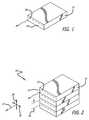
- FIG. 1is a perspective view of an embodiment laser emitter bar.
- FIG. 2is a perspective view of an embodiment of a stacked array of laser emitter bars.
- FIG. 3shows an emission array of the laser emitter bars of the stacked array embodiment of FIG. 2 .
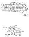
- FIG. 4is an elevation view in partial section of an embodiment of a laser emitter module.
- FIG. 4Ais a perspective view of a portion of an embodiment of a laser emitter module partially cut away.
- FIG. 5is an elevation view in partial section of an embodiment of a ferrule assembly secured to a wall of a laser emitter module housing.
- FIG. 6is a perspective view of an embodiment of a mounting assembly for mounting a laser emitter bar and fast axis collimator to a base of a housing.
- FIG. 7is perspective view of an embodiment of a base and side wall portion of an enclosure of a laser emitter module having a large aperture in a wall thereof.
- FIG. 8is an elevation view in partial section of an embodiment of a laser emitter module.
- FIG. 9is an elevation view of an embodiment of a housing of a laser emitter module having a front surface in contact with a datum block.
- FIG. 10is a top view of the laser emitter module of FIG. 9 .
- FIG. 11is an enlarged view of a reticle aligned with a front and side surface of a laser emitter bar.
- FIG. 12is a schematic view of an embodiment of a housing for mounting of a laser emitter bar with an open top portion and an embodiment of a beam profile device aligned with an output beam of the laser emitter bar.
- FIG. 13is an elevation view of an embodiment of a beam conditioning optic.
- FIG. 14is a perspective view of the beam conditioning optic of FIG. 13 .
- FIG. 15is an elevation view in partial section of an embodiment of a ferrule assembly secured to a wall of a laser emitter module housing.
- FIG. 16is a transverse cross section of the ferrule assembly of FIG. 15 taken along lines 16 - 16 of FIG. 15 .
- Embodiments discussed hereinare directed to methods and devices for packaging emitters such as laser emitter bars or chips having one or more emitters disposed therein. Embodiments discussed herein are also directed to methods and devices for coupling an output of laser emitter bars to an optical conduit, such as an optical fiber. Such bars or chips may be mounted to or otherwise incorporated into optical system embodiments by a variety of methods. For such optical packages, it is important that the output array of the chips be properly aligned, that such alignment may be carried out conveniently and accurately and that the final configuration dissipate the heat generated by the chip efficiently. For some embodiments, it may also be important that an enclosure of the optical components be hermetically sealed in order to provide reliability and consistency in the output of the assembly embodiments.
- FIG. 1shows a laser emitter bar 12 having an output surface 14 that includes a total of 5 emitters 16 which have optical axes that are substantially parallel to each other.
- FIGS. 2 and 3show a stacked array 10 of 4 laser emitter bars 12 .
- Each laser emitter bar 12has an output surface 14 that includes a total of 5 emitters 16 disposed adjacent each other.
- the emitters 16 of each bar 12are disposed in a substantially linear row along a slow axis direction of the emitters 16 , as indicated by arrow 18 .
- a fast axis direction of the emitters 16is perpendicular to the slow axis direction 18 and is indicated by arrow 20 .
- the emitters 16are positioned or otherwise configured so as to emit light energy in output beams that propagate along an emission axis 22 which may be perpendicular to both the slow axis direction 18 and fast axis direction 20 .
- the emission axes 22 of the emitters 16 of the stacked arraymay be substantially parallel to each other.
- the laser emitter bars 12are stacked along a fast axis direction 20 of the emitters 16 and may be stacked in a periodic and regular distribution.
- the emitters of a bottom laser emitter bar 12are vertically separated from the emitters of an adjacent laser emitter bar 12 by a distance indicated by arrow 24 which may be referred to as the pitch of the stacked array 10 .
- the pitch indicated by arrow 24may be about 1 mm to about 3 mm, specifically, about 1.5 mm to about 2.0 mm.
- Such a stacked array 10 of laser emitter bars 12 and emitters 16may allow a large amount of light energy or power to be produced in a compact device for some embodiments.
- Laser emitter bar embodiments 12may have any suitable number of emitters 16 , such as about 1 emitter to about 100 emitters, more specifically, about 3 emitters to about 12 emitters.
- each laser emitter bar 12 having about 5 emitters 16may have an output power of about 5 W to about 50 W, more specifically, about 10 W to about 20 W.
- Emitters 16may include laser diodes such as edge emitting laser diodes, vertical cavity surface emitting lasers (VCSELs) and the like.
- Materials for the emitters 16 of the laser emitter bar 12may include semiconductor materials such as GaAs, InP or any other suitable laser gain medium.
- the emitting aperture of a laser diode embodiment of an emitter 16is rectangular in shape with the long dimension of the emitter 16 having a size of typically tens or hundreds of microns, while the short dimension is typically one to several microns in size. Radiation emerging from an emitter 16 diverges with the divergence angle being greater along the short emitter 16 direction. Divergence angles are lower in the direction of the long emitter 16 direction.
- Some embodiments of the emitters 16may have a physical width of about 50 microns to about 300 microns, a height of about 1 micron to about 3 microns, and a cavity length of about 0.5 mm to about 5 mm.
- Such emitter 16 embodimentsmay have a divergence of light energy output of about 2 degrees to about 12 degrees in the slow axis direction 18 and a divergence of light energy output of about 30 degrees to about 75 degrees in the fast axis direction 20 .
- Some embodiments of the laser diode bars 12may have emitters 16 that emit light energy having a wavelength of about 700 nm to about 1500 nm, more specifically, about 800 nm to about 1000 nm. Emitters 16 may emit light having a centroid or peak wavelength of about 300 nm to about 2000 nm, more specifically, of about 600 nm to about 1000 nm, including wavelengths across the near infrared spectrum. Some particular embodiments of useful emitters may emit light at a peak wavelength of about 350 nm to about 550 nm, 600 nm to about 1350 nm or about 1450 nm to about 2000 nm. Such laser diode bars may be operated in either a pulsed mode or continuous wave mode.
- the output spectral band of individual emitters 16 which are not wavelength controlledmay be about 0.5 nm to about 2.0 nm or more. Due to the variation in peak emission wavelength in addition to the spectral band for each individual emitter, the overall bandwidth of the laser emitter bar 12 may be about 2 nm to about 5 nm, for some embodiments.
- Stacked array 10includes 4 laser emitter bars 12 , however, other embodiments of stacked arrays 10 may have any suitable number of laser emitter bars 12 . Some stacked array embodiments 10 may have about 2 laser emitter bars 12 to about 30 laser emitter bars 12 , more specifically, about 2 laser emitter bars 12 to about 10 laser emitter bars 12 .
- stacked array 10is shown with a fast axis collimator 26 in the form of a cylindrical lens array optionally disposed over the emitters 16 of the stacked array 10 and configured to substantially collimate an output beam of the emitters 16 of each laser emitter bar 12 in a fast axis direction 20 .
- a fast axis collimator 26in the form of a cylindrical lens array optionally disposed over the emitters 16 of the stacked array 10 and configured to substantially collimate an output beam of the emitters 16 of each laser emitter bar 12 in a fast axis direction 20 .
- Fast axis collimator 26may include one cylindrical lens for each laser emitter bar 12 or one or more monolithic lens arrays as well as any other suitable configuration.
- This fast axis collimation of the emitter outputproduces an output array 28 as shown wherein the light energy output 30 of each emitter 16 of each laser emitter bar 12 is substantially collimated along the fast axis 20 of the emitters 16 but continues to diverge along the slow axis 18 of the emitters 16 .
- the light energy outputs 30 of each laser emitter bar 12may have a substantially rectangular cross section transverse to the direction of propagation and are parallel to each other so as to produce the output array 28 as shown.
- any variety of beam condition devicesmay be positioned on or in close proximity to the output surface 14 . Exemplary beam conditioning devices include, without limitations, volume Bragg grating, gratings, beam combiners, polarizers, beam twisters, and the like.
- FIGS. 4-7illustrate an embodiment of an optical apparatus assembly 40 in the form of a laser emitter module for coupling the output of a laser emitter bar 12 into an input surface 42 of an optical fiber 44 .
- the assembly 40includes a hermetically sealed enclosure in the form of a housing 46 having a base 48 , a lid 50 , and side walls 52 which are disposed between the base 48 and the lid 50 .
- An aperture 54is disposed in a wall 52 opposite the laser emitter bar 12 and is configured to accept an adjustable ferrule assembly 56 having a radially extending flange 58 which may be sealingly secured to a wall of the enclosure 46 .
- the aperture 54may also be sized to as to allow an output 30 of the laser emitter bar 12 to pass through the aperture 54 in order to actively align the optical components of the apparatus 40 as will be discussed in more detail below. More specifically, the aperture 54 may be a relatively large aperture 54 disposed in a wall of the enclosure 46 which is substantially aligned with an output axis 60 of the laser emitter bar 12 . A transverse dimension and position of the aperture 54 relative to the laser emitter bar 12 may be configured to allow substantially all of the emitted light output 30 of the laser emitter bar 12 from a fast axis collimator 62 or other collimating optic to pass through the aperture 54 .
- the aperture 54may have a transverse dimension of about 3 mm to about 20 mm, more specifically, about 5 mm to about 10 mm.
- laser emitter bar 12is shown with 5 emitters 16
- the module 40may include a laser emitter bar 12 having any suitable number of emitters 16 as discussed above.
- the housing 46also includes one or more apertures disposed on a wall opposite the aperture 54 that is configured to accommodate a plurality of high current electrical conductors.
- a first electrical conductor 64 and second electrical conductor 66are used to provide electrical power to the interior of the housing 46 for powering the laser emitter bar or bars 12 disposed within the housing 46 .
- the conductors 64 and 66may include solid conducting material or be configured as a multifilament braid or strand for flexibility.
- the conductors 64 and 66may be made from materials having high degree of electrical conductivity such as copper, silver, gold or the like.
- Portions of the conductors 64 and 66are secured in a fixed and sealed relation to a flange member 58 that may in turn be secured in a fixed and sealed relation to a wall 52 of the housing 46 .
- the seal between the conductors 64 and 66 and the flange 58 and the flange 58 and the housing 46may be a hermetic seal for some embodiments.
- a thermally conductive and electrically insulative heat sink spacer 70may be secured to an inside surface 72 of the base 48 with a bonding agent layer (not shown) disposed between the heat sink spacer 70 and base 48 .
- the heat sink spacer embodiment 70 shownis substantially rectangular having an upper surface which is substantially parallel to a lower surface thereof.
- the heat sink spacer 70may be configured to provide a thermally conductive and electrically insulative platform upon which to mount a heatsink 74 .
- the heatsink 74may be used as a platform to mount the laser emitter bar 12 of the module 40 .
- the laser emitter bar 12may be secured to the heatsink 74 with thermally conductive adhesive bonding, thermal compression bonding, soft solder, hard solder, including gold tin solder or the like.
- the bonding agent layer between the heat sink spacer 70 and the base 48may include hard solder, soft solder, thermally conductive adhesive such as silver epoxy or silver glass, welding, glass attaching or the like.
- Suitable solders for the bonding agent layer between the heat sink spacer 70 and the base 48may include InSn, AgSn, AuGe and AuSn solders as well as others.
- the Au concentrationmay be about 80 percent to about 86 percent relative to the Sn concentration.
- the use of soft soldermay serve to isolate the heatsink spacer 70 from thermal expansion and/or distortion of the base 48 .
- a hard soldermay have a melting point of at least about 280 degrees Celsius and a soft solder may have a melting point below about 280 degrees Celsius.
- the bonding agent layer between the heat sink spacer 70 and the base 48may have a thickness of about 10 microns to about 150 microns.
- the thermal conductivity of the heat sink spacer 70may provide a conduit for the dissipation of thermal energy produced by the laser emitter bar 12 which passes through the heatsink 74 .
- the insulative electrical properties of the heat sink spacer 70may be configured to electrically isolate the laser emitter bar 12 from the base 48 and enclosure 46 generally.
- a thermally conductive and electrically insulative material of the heat sink spacer 70may include a ceramic such as aluminum nitride as well as other suitable materials.
- the heatsink spacer 70may also include a material having a coefficient of thermal expansion that substantially matches the coefficient of thermal expansion of the base 48 of the enclosure 46 .
- the heatsink spacer 70may have a Young's modulus of about 1.5 ⁇ 10 11 Pa to about 4 ⁇ 10 11 Pa, more specifically, about 3 ⁇ 10 11 Pa to about 3.5 ⁇ 10 11 Pa.
- the heatsink spacer 70may have a thickness of about 0.5 mm to about 5 mm, more specifically, about 1 mm to about 3 mm
- the heatsink element 74 for dissipation of heat generated by the laser emitter bar 12may be secured to a top surface of the heat sink spacer 70 by a bonding agent layer (not shown) disposed between a top surface of the heat sink spacer 70 and a bottom surface of the heat sink element 74 .
- the laser emitter bar 12may be secured to a top surface of the heat sink element 74 by a variety of suitable methods.
- the heat sink element 74may be rectangular in shape with an upper surface that is substantially parallel to a bottom surface thereof.
- the heat sink element 74may be made from a thermally conductive material that may be electrically conductive for some embodiments and electrically insulative for other embodiments.
- the heatsink element 74may have a thickness of about 0.5 mm to about 5 mm, more specifically, about 1 mm to about 3 mm.
- the bonding agent layer between the heat sink spacer 70 and the heat sink element 74may include hard solder, soft solder, thermally conductive adhesive such as silver epoxy or silver glass, welding, glass attaching or the like.
- Suitable solders for the bonding agent layer between the heat sink spacer 70 and the heat sink element 74may include silver tin AgSn, indium silver InAg, gold germanium AuGe and gold tin AuSn solders.
- the AuSn soldermay have an Au concentration of about 80 percent to about 86 percent relative to the Sn concentration.
- the coefficient of thermal expansion of the heatsink element 74may be desirable for substantially match a coefficient of thermal expansion of the heat sink spacer 70 .
- the heat sink spacer 70may be made of aluminum nitride having a coefficient of thermal expansion of about 4.2 ppm per degree Celsius and the heatsink element 74 may be made from copper tungsten having a coefficient of thermal expansion of about 6.5 ppm per degree Celsius.
- a soft soldersuch as AgSn or InAg may be desirable for the bonding agent layer.
- the bonding agent layer between the heat sink spacer 70 and the heat sink elementmay have a thickness of about 10 microns to about 150 microns.
- An optional optical substrate 76may also secured to an upper surface of the heat sink spacer 70 with the fast axis collimator 62 secured to an upper surface of the optical substrate 76 .
- the optical substrate 76may include a ceramic or glass having a low thermal conductivity and may have a coefficient of thermal expansion that is substantially the same as the coefficient of thermal expansion of the heat sink spacer 70 .
- the optical substrate 76may be secured to the heatsink spacer 70 by soldering, welding or glass attaching for some embodiments.
- the optical substrate 76may be secured to the heatsink spacer 70 by epoxy bonding.
- the heat sink spacer 70may serve to mechanically isolate the laser emitter bar 12 , fast axis collimator 62 and optical substrate 76 from the housing 46 .
- FIG. 4shows an organic getter assembly 76 A secured to the inside surface of the cover 46 and an organic getter assembly 76 B clipped to the base 48 .
- Such getter assemblies 76 A and 76 Bmay be included in any of the module embodiments discussed herein.
- the organic getter assemblies 76 A and 76 Bmay be configured to absorb organic outgassing that occurs within the interior of the module 40 .
- Such organic getter assembliesmay be included within any of the module assembly embodiments discussed herein.
- the fast axis collimator 62is secured in a fixed position adjacent an output surface 14 of the laser emitter bar 12 .
- the fast axis collimator 62which may include an elongate cylindrical lens, may be configured to substantially collimate the output of the laser emitter bar 12 in a fast axis direction.
- the fast axis collimator 62may be secured to the optical substrate 76 by soldering, welding or glass attaching.
- the fast axis collimator 62may be secured to the optical substrate 76 by epoxy bonding.
- a beam conditioning elementmay be secured to the top surface of the optical substrate 76 in addition to the fast axis collimator 62 .
- one or more beam conditioning optics 77may be disposed in the optical train of the module 40 between the fast axis collimator 62 and optional optical components 90 , or any other suitable position.
- Such beam conditioning optics 77may be secured separately from or in combination with the fast axis collimator 62 as a sub-assembly.
- the beam conditioning optics 77are secured in fixed relation to the base 48 of the housing 46 by securing the conditioning optics 77 to the optical substrate 76 which is, in turn, secured to the respective heat sink spacer.
- the beam conditioning optic 77may be secured to the optical substrate 76 , heat sink, heat sink spacer or directly to the base 48 by soldering, welding, glass bonding, adhesive bonding including epoxy bonding or the like.
- the beam conditioning optic 77may be actively positioned prior to being secured in fixed relation to the housing 46 by the methods of active alignment discussed herein. Beam slope and edge sharpness, location of the spots in reference to a virtual reference set from a facet of a corresponding laser emitter bar 12 , and total far field beam size are factors that may be considered in optimizing the alignment.
- Some embodiments of the beam conditioning optic 77may serve as a beam reformatting optic that serves to twist individual beamletts around an axis of propagation or re-format a horizontally adjacent segment to a vertical orientation.
- the beam conditioning optic 77may have an optional handle portion 77 A secured to the optic 77 so as to facilitate handling of the optic 77 during assembly of the module 40 .
- the handle portion 77 Amay include a block of rigid or semi-rigid material that is secured to the optic 77 by adhesive bonding, soldering or the like such that the handle portion 77 A extends from an upper surface of the optic 77 . This may allow the optic 77 to be grasped and positioned by tweezers or other handling equipment during assembly without making contact with the critical input and output surfaces of the optic 77 .
- the handle portion 77 Amay also be secured to either side of the optic 77 .
- the material of the handle portionmay be a material similar to that of the optic 77 such as glass, quartz, silica or the like for some embodiments.
- Such handle portions 77 Amay also be secured to any of the other optical components discussed herein to facilitate assembly of the module embodiments.
- module 40does not include optical substrate 76 and has the beam conditioning optic 77 secured to the heat sink spacer 70 by means of a pair of wedge shaped prism members 75 .
- the prism members 75have a bottom surface secured directly to the heat sink spacer 70 with adhesive bonding, soldering or the like.
- a side surface of each respective prism member 75is secured to an opposing lateral side of the beam conditioning optic 77 by the same or similar method as used for the bond with the heat sink spacer 70 .
- the beam conditioning optic 77is positioned in front of and aligned with an output of the laser emitter bar 12 .
- the material of the prism members 75may be a material similar to that of the optic 77 such as glass, quartz, silica or the like for some embodiments.
- the fast axis collimator 62for the embodiment shown in FIG. 4A , is secured directly to a rear surface of the beam conditioning optic 77 .
- the side surfaces of the fast axis collimator 62may also be secured to respective side surfaces of the prism members 75 .
- Embodiments of beam conditioning opticsare described in U.S. patent application Ser. No. 11/747,184, titled “Multiple Emitter Coupling Devices and Methods with Beam Transform Systems”, filed May 10, 2007, by Y. Hu et al., which is incorporated by reference herein in its entirety.
- U.S. patent application Ser. No. 11/747,184discusses a variety of beam transform systems which may be used as a beam conditioning optic 77 for the laser emitter module embodiments discussed herein.
- One such beam conditioning or transform opticis shown in FIGS. 13 and 14 herein and discussed further below.
- a slow axis collimator 78configured to collimate an output of the laser emitter bar 12 in a slow axis direction 18 of the output beam may also be secured to the base 48 shown in FIG. 4 .
- the slow axis collimator 78may include a cylindrical lens or lens array configured to carry out collimation of the output of the laser emitter bar 12 .
- the slow axis collimator 78may be secured in fixed relation to the base by soldering, welding, glass bonding or the like as well as with the use of epoxy bonding for some embodiments.
- the slow axis collimator 78may be actively positioned prior to being secured by any of the methods of active alignment discussed herein.
- the optical fiber 44is disposed within and secured to the adjustable ferrule assembly 56 that includes an outer sleeve having central tubular barrel 80 and a flange portion 82 that extends radially from the barrel 80 .
- the barrel 80includes a substantially concentric inner lumen 81 that extends from a first end of the barrel 80 to a second end of the barrel 80 .
- the flange portion 82may include a flat inner surface 84 configured to mate with an outer surface of the wall 52 of the enclosure adjacent the aperture 54 .
- the flange portion 82also has an outer transverse dimension greater than an outer transverse dimension of the aperture 54 .
- the flange portion 82may also include a shallow cylindrical boss portion 86 with a transverse dimension less than a transverse dimension of the aperture 54 such that the boss portion 86 may mechanically engage the aperture 54 and be moved transversely to allow for adjustment of a position of the optical fiber input surface 42 prior to securing the ferrule 56 in fixed relation to the enclosure 46 .
- a cylindrical fiber attachment sleeve 83 having an input end 85is configured to slide axially within the inner bore 81 of the outer sleeve barrel 80 and has an axial fiber receiving lumen 87 disposed concentrically with an outer surface thereof.
- An outer surface of the optical fiber 44may be secured within the axial lumen 87 of the attachment sleeve 83 by a variety of suitable methods including crimping, soldering, brazing, welding, adhesive bonding or the like.
- a jacketed portion of the optical fiber 44 disposed proximal of the input end 42may be potted in an adhesive 87 A as shown, or otherwise secured to an inside surface of the fiber attachment sleeve 83 .
- a resilient strain relief element 87 B having a tapered configurationmay also be disposed over the optical fiber 44 proximal of and secured to the attachment sleeve 83 so as to prevent damage to the optical fiber 44 as a result of bending stress.
- the input end 42 of the optical fiberis disposed axially beyond the input end 85 of the fiber attachment sleeve 83 and within the inner bore 81 of the outer sleeve 80 .
- This configurationallows the flange portion 82 to be seam welded or laser seam welded to the wall 52 of the housing 46 with a minimum of mechanical distortion of the position of the input end 42 of the fiber 44 relative to the housing as a result of the welding process.
- This configurationmay also serve to protect the input end 42 of the optical fiber 44 from contamination during laser seam welding of the outer sleeve 80 to the wall 52 of the housing for embodiments utilizing a welding attachment method.
- the input end 42 of the fiber 44may be recessed within the inner lumen 81 from a front end of the boss 86 by an axial distance of about 0.5 mm to about 2 mm.
- the inner lumen 81may have an inner transverse dimension or diameter of about 1 mm to about 3 mm.
- the outer sleeve 80may be made from materials such as Kovar®, stainless steel such as 304L stainless steel, nickel such as 201 nickel.
- the outer sleeve 80may include suitable materials for laser welding that does not produce micro-cracks during laser seam welding to keep the module hermetically sealed.
- the fiber attachment sleeve 83 , the outer sleeve 80 and the surface 84may include a coating that is configured to protect raw metal from corrosion.
- a corrosion protection coatingmay include an electrolytic nickel plating or any other coating material suitable for laser welding that does not produce micro-cracks during laser seam welding to keep the module hermetically sealed.
- the outer sleeve 80 , fiber attachment sleeve 83 or bothmay be made from materials such as Arcap® or other materials suitable for soldering or epoxy attachment.
- the input end 42 of the optical fiber 44may extend from the input surface 85 of fiber attachment sleeve 83 a length of about 0.5 mm to about 1 mm.
- the flange portion 82may be seam welded around its entire circumference to the wall 52 of the housing 46 to produce a hermetic seal between the outer sleeve 80 and the housing 46 .
- the fiber attachment sleeve 83may also be seam welded around an entire circumference of an outer surface thereof the a proximal portion of the outer sleeve 80 to produce a hermetic seal between the outer sleeve 80 and the fiber attachment sleeve 83 .
- a hermetic seal between an outer surface of the fiber 44 and the housingmay be produced that produces a reliable seal and also allows for adjustment of radial and axial position of the input end 42 of the optical fiber 44 during assembly of the apparatus 40 .
- the lid 50 of the enclosure 46may also be secured to the housing 46 by a hermetic sealing technique such as soldering, laser seam welding or the like. As such, a hermetic seal may be created between an outer surface of the optical fiber 44 and an interior cavity of the enclosure 46 as a whole.
- a focusing element 88may be disposed in an optical train of the apparatus 40 extending from the emitters 16 of the laser emitter bar 12 .
- the focusing element 88may be configured to focus an output of the laser emitter bar 12 into an input surface 42 of the optical fiber 44 .
- the focusing element 88may include one or more cylindrical lenses configured to focus the output beam of the laser emitter bar 12 in both the fast axis 20 and slow axis 18 for some embodiments.
- the focusing element 88may be secured in fixed relation to the base 48 of the enclosure 46 by a variety of suitable methods including soldering, welding including laser welding, glass attach and the like. Epoxy bonding may also be used to secure the focusing element 88 for some embodiments.
- the focusing element 88may be actively positioned prior to being secured by any of the methods of active alignment discussed herein.
- Optical components 90in addition to those discussed above may also be operatively disposed within an optical train of the apparatus may include lenses, filters, prisms, polarizers, waveplates, such as 1 ⁇ 4 waveplates and 1 ⁇ 2 waveplates. Such components may be used to condition the output of the laser emitter bar 12 in order to further enhance the coupling of the output to the optical fiber.
- optical component 90may include a spectral band conditioning element, such as a Volume Bragg Grating (VBG), may be used to narrow or otherwise condition the output beam of the emitters 16 .
- VBGVolume Bragg Grating
- the optical fiber 44 of the apparatus 40may be coupled to an optical component to provide the optical component with a light energy source.
- the optical componentmay be a laser, including optical fiber lasers and the like, which is coupled to the apparatus 40 for purposes of providing pump energy or the like. In such configurations, it may be important to prevent light energy from the optical component to be reflected or otherwise transmitted back into a laser emitter bar 12 of the apparatus 40 . Such reflected or leaked light energy entering the apparatus and particularly the laser emitter bar 12 may be damaging to the apparatus. This may be particularly true where the optical component is capable of producing high energy pulsed light that is transmitted back to the apparatus 40 through the fiber 44 .
- the apparatus 40may have a configuration that prevents such reflected light energy from reaching the laser emitter bar 12 .
- optical components, such as lasers, coupled to the apparatus 40may operate at a spectral band that is different from the output spectral band of the laser emitter bar 12 of the apparatus 40 .
- a reflective coatingmay be disposed on one or more of the optical elements within the apparatus 40 that reflects light energy at the spectral band of the optical component coupled to the apparatus 40 but transmits light energy of a spectral band of the laser emitter bar 12 of the apparatus. It may also be desirable to include an antireflective coating on one or more of the optical elements of the apparatus that is antireflective at the spectral band of the laser emitter bar 12 .
- an optical component coupled to the laser emitter module 40may be configured to receive the output spectral band of the laser emitter bar and communicate light energy having a spectral band different from the spectral band of the laser emitter bar 12 back to the laser emitter module.
- a reflective coatingmay be disposed on an optical element of the laser emitter module and configured to reflect the spectral band communicated by the optical component coupled to the laser emitter module and transmit the spectral band of the laser emitter bar 12 .
- Optical elements of the apparatus 40may include the fast axis collimator 62 , the slow axis collimator 78 , the focusing element 88 or other optical elements 90 that may include beam conditioning optics and the like.
- beam conditioning opticsmay include a beam re-formatting element which may be configured to twist individual beamletts around an axis of propagation or re-format a horizontally adjacent segment to a vertical orientation.
- the spectral band of the laser emitter bar 12may have a centroid wavelength of about 750 nanometers to about 999 nanometers, more specifically, about 900 nanometers to about 995 nanometers.
- Some embodiments of the reflective coatingmay be configured to reflect a spectral band having a centroid wavelength of about 1000 nanometers to about 1095 nanometers. Such a configuration may be suitable for an apparatus 40 coupled to an optical component that operates at a spectral band having a centroid wavelength of about 1000 nanometers to about 1095 nanometers and a laser emitter bar 12 having a spectral band output with a centroid wavelength of about 900 nanometers to about 995 nanometers.
- the reflective coatingmay include silicon dioxide, alumina, titanium oxide, tantalum oxide, zirconium oxide and halfnia as well as other suitable materials.
- the desired effect described abovemay be achieved with the use of appropriately chosen reflective and antireflective coatings, the same or similar effect may be achieved with one or more optical isolators (not shown) disposed within or adjacent the laser emitter module 40 .
- such an optical isolatormay have a high level of transmission at emitter wavelengths of about 750 nanometers to about 999 nanometers, more specifically, about 900 nanometers to about 995 nanometers, when that radiation is directed towards an input end 42 of optical fiber 44 .
- Some such isolator embodimentsmay also have low optical transmission or high reflectivity of light energy having a wavelength of about 1000 nanometers to about 1150 nanometers or more, more specifically, about 1040 nanometers to about 1095 nanometers, directed in a direction different from that of the output of the emitters, such as from the optical fiber 44 towards the emitters.
- suitable optical isolatorsmay include a first polarizing element that transmits light energy that has a polarization orientation substantially parallel to the polarization of laser emitter bar 12 , a polarization rotating element and a second polarizing element that is oriented such that it is highly transmissive to light energy from the laser emitter bar 12 but substantially non-transmissive to light energy propagating in the opposite direction towards the laser emitter bar 12 .
- FIG. 8illustrates an embodiment of an optical apparatus assembly 92 for coupling the output of the laser emitter bar 12 with an input surface 42 of an optical fiber 44 .
- the apparatus embodiment 92 of FIG. 8may have some of the same or similar features, dimensions and materials as the features, dimensions and materials of the apparatus 40 discussed above with regard to FIGS. 4-7 .
- the heat sink element 94may include an upper layer of thermally conductive and electrically insulative material 96 which may obviate the need for such properties in the heatsink spacer element 98 of the assembly 92 . More specifically, the heat sink spacer element 98 may still require relatively high thermal conductivity but may be made of an electrically conductive material.
- the apparatus 92includes a housing 46 having a base 48 , side walls 52 and a lid 50 .
- a heat sink spacer embodiment 98is secured to an inside surface of the base 48 .
- Embodiments of the heatsink spacer 98may include ceramic or metal. Metal materials may be acceptable for construction of some embodiments because of an electrically insulative layer which is on the upper surface of the heat sink 94 which is secured to a top surface of the heat sink spacer 98 .
- the heatsink element 94includes the upper layer of thermally conductive and electrically insulative material 96 which is disposed on the upper level of the heatsink 94 and forms the top surface of the heatsink 94 .
- the thermally conductive and electrically insulative material 96may include a ceramic material such as aluminum nitride and may serve to electrically isolate the laser emitter bar 12 from the base 48 .
- the heatsink element 94may have a thickness of about 0.5 mm to about 5 mm, more specifically, about 1 mm to about 3 mm, and the upper layer of thermally conductive and electrically insulative material 96 may have a thickness of about 100 microns to about 500 microns, more specifically, about 300 microns to about 400 microns.
- the laser emitter bar 12may be secured to the thermally conductive and electrically insulative upper layer 96 of the heat sink 94 by suitable methods such as thermally conductive adhesive bonding, thermal compression bonding or the like.
- An optical substrate 76is also secured to a top surface of the heat sink spacer 98 by any suitable method.
- a fast axis collimator 62is secured to the optical substrate 76 adjacent an output surface 14 of the laser emitter bar 12 and is configured to substantially collimate the output of the laser emitter bar 12 in a fast axis direction 20 .
- Optional beam conditioning optic 77may be similarly mounted or secured between the fast axis collimator 62 and optic 90 as shown.
- the laser emitter bar 12 and optical elements of the laser emitter modules 40 and 92need to be properly aligned along an optical axis of the devices.
- One means for achieving a high level of such optical alignmentis to use an active alignment technique whereby the optical elements of the module are aligned while the emitters 16 of the laser emitter bar 12 are emitting light energy through the optical element.
- the output of the laser emitters 16 of the laser emitter bar 12must be accessible to diagnostic equipment use to monitor beam quality emanating from the optical elements.
- the large aperture 54allows such access, provided the output 30 of the laser emitter bar 12 is sufficiently aligned to as to pass substantially through the large aperture during operation.
- an arrangementsuch as shown in FIGS. 9-11 may be used.
- a method of aligning a laser emitter moduleinclude positioning a housing 46 of a laser emitter module 40 against a datum surface or point so as to determine the orientation and position of a selected surface, such as the front surface 100 , of the housing relative to an external reference member.
- FIGS. 9 and 10show the front surface 100 of the housing 46 of the laser emitter module 40 disposed firmly against a mating surface of a datum block 102 such that the position of the front surface 100 of the housing 46 is known relative to the datum block 102 .
- the position of the housing 46 relative to the datum block 102is further restrained by the penetration of a tapered conical plug 104 into the aperture 54 of the housing 46 .
- the mating surface of the datum block 102prevents front to back motion of the housing 46 and the tapered conical plug 104 prevents lateral or side to side motion as well as vertical motion of the housing 46 relative to the datum block 102 .
- the conical plug 104may be biased by a resilient force such as a spring force in a forward direction such that the mating conical surface of the conical plug 104 engages the aperture 54 with a constant engaging force to help maintain the position of the housing 46 relative to the datum block 102 .
- An imaging devicesuch as a CCD camera 106
- the camera 106is in fixed relation to the datum block 102 such that position relative to the datum block may also be used to determine position relative to the field of view of the camera 106 .
- the field of view of the camera 106includes a reticle 108 having two lines perpendicular to each other that indicate the proper position of the forward facet of the laser emitter bar 12 in order to achieve proper alignment of the optical axis of the laser emitter bar output with the aperture 54 of the housing.
- the position and orientation of a facet of a laser emitter bar 12 relative to the external reference member 102may then be used to align the laser emitter bar 12 relative to the housing 46 such that a majority of an output from the laser emitter bar 12 will pass through the aperture by aligning the front facet and side surface of the laser emitter bar 12 with the corresponding lines of the reticle 108 .
- Fine adjustment of the position of the laser emitter barmay be carried out with robotic tools that may include pneumatic tweezers and the like that may be precisely positioned with respect to the housing.
- FIG. 12illustrates the housing 46 and laser emitter bar 12 assembly disposed in functional relation with a beam profiling assembly 110 .
- the housing 46is positioned such that the output axis of the laser emitter bar 12 is oriented towards an input of the beam profiling assembly 110 .
- the aperture 54 in the front of the housing 46is open so as to allow the output of the laser emitter bar 12 to pass through the aperture 54 and be monitored and characterized by the beam profiling device 110 during embodiments of the active alignment process.
- the housing 46may be secured in fixed relation to a datum block (not shown) which may be similar to the datum block 102 discussed above.
- the housing 46 and datum blockmay in turn be secured to the assembly 110 that is configured to move in up to six degrees of freedom with respect to the optical element 62 , 78 , 88 or 90 in order to make the appropriate angular adjustments during the active alignment process of optical elements.
- the roll, pitch and yaw of the laser emitter bar 12may be adjusted relative to the optical elements to be positioned as well as X axis, Y axis and Z axis translation of the laser emitter bar 12 relative to the optical axis of the optical element being positioned.
- the optical elements to be positioned within the housing 46include the fast axis collimator 62 , the slow axis collimator 78 , the focusing element 88 as well as any other beam conditioning optics 90 . Although some embodiments of alignment methods are directed to mounting various optical elements in a specific order, for other embodiments, the optical elements may be mounted in any desired order.
- the beam profiling assembly embodimentincludes a beam splitter 112 , a pinhole element 113 disposed in front of a reference laser 114 , a first beam attenuator 116 , a second beam attenuator 118 , a beam stop 120 , a first set of neutral density filters 124 , a first lens 126 , a first CCD camera 128 having a first CCD plane 130 .
- the assemblyalso includes a second set of neutral density filters 132 , a second lens 134 and a second CCD camera 136 having a second image plane 138 .
- the housing 46 with the laser emitter bar 12 secured theretois positioned in front of the beam profiling device 110 prior to the addition of any other optical elements such as the fast axis collimator 62 , slow axis collimator 78 , focusing element 88 or other beam conditioning components 90 .
- the reference laser 114may be activated.
- the reference laser 114may be a helium neon laser, a low power red semiconductor laser or the like with a collimated output beam.
- the reference beam from the reference laser 114travels through the pinhole 113 , is reflected from the beam splitter 112 through the aperture 54 and onto the front facet surface of the laser emitter bar 12 or reference reflector which may be located at a front facet location.
- the reference beamis then reflected from a front facet of the laser emitter bar 12 or reference reflector which is located at a front facet location of the laser emitter bar 12 .
- the reference laser 114may be adjusted in order for the reflected beam from the front facet to be aligned with the pinhole 113 . Thereafter, the reference laser beam may define the optical axis of the laser emitter bar as it will be perpendicular to the front facet or output surface 14 of the laser emitter bar 12 .
- a portion of a facet on a front surface of the laser emitter bar 12may have a metal portion to increase the reflectivity of the surface.
- metalssuch as gold may be used to increase the reflectivity of the laser emitter bar 12 facet.
- the reference beam reflected from the front facet of the laser emitter bar 12may then be imaged by the first CCD camera 128 .
- the point of impingement of the reference beam measured by the first CCD camera 128may be used to determine the optical axis of the laser emitter bar 12 . If the optical axis of the laser emitter bar 12 is not aligned, the position of the housing 46 may be adjusted until the optical axis of the emitter bar 12 is properly aligned.
- the optical elementsmay be individually added, actively aligned and then secured in fixed relation to the housing 46 .
- 2 or more optical elementssuch as optical elements 62 , 78 , 88 and 90 , may be pre-attached in a sub-assembly and then the sub-assembly actively aligned and secured to housing 46 .
- the fast axis collimator 62may be gripped by tweezers such as pneumatic tweezers, and positioned in front of the output surface 14 of the laser emitter bar 12 .
- the emitters 16 of the laser emitter bar 12may then be activated and the output beam of the laser emitter bar 12 monitored to determine the quality of alignment of the fast axis collimator 62 with respect to the optical axis of the laser emitter bar 12 .
- the first beam attenuator 116 and the second beam attenuator 118are used to attenuate the power of the beam by reflecting the wavelength of light energy being emitted from the laser emitter bar 12 .
- the first set of neutral filters 124 and second set of neutral density filters 132are used to reduce the intensity of the output of the laser emitter bar 12 in order to produce a beam intensity that is suitable for imaging by the first and second CCD cameras 128 and 136 .
- the quality of alignment of the fast axis collimator 62is evaluated by measuring the angular distribution of the output beam which has been converted from spatial distribution of the output beam by the first lens 126 .
- the angular distributionis measured with the first CCD camera 128 .
- the beam location at the aperture 54is also monitored by imaging the output beam at the aperture 54 of the housing with the second CCD camera 136 which may be used to measure the alignment of the optical axis of the output from the fast axis collimator 62 .
- the alignment of the fast axis collimator 62is adjusted until the beam position on the first and second CCD cameras, beam divergence and edge sharpness in a fast axis direction achieve a desired level or is otherwise optimized.
- the fast axis collimatormay be secured in fixed relation to the housing 46 and laser emitter bar 12 .
- the fast axis collimator 62may be secured with a mount portion of the fast axis collimator 62 contacting a mount portion of the optical substrate 76 by soldering, welding including laser welding, brazing, adhesive bonding or any other suitable method.
- the output signal of the first and second CCD cameras 128 and 136 or other imaging devicemay be monitored visually on the video display or may be monitored by other suitable display devices and methods.
- the fast axis collimatormay be pre-assembled with the beam conditioning optic 77 .
- the beam conditioning optic 77may also be separately aligned and attached to the optical substrate 76 , or a second optical substrate (not shown) either on the heat sink spacer 70 or package base 48 .
- the slow axis collimator 78may then be gripped by tweezers such as pneumatic tweezers, and positioned in front of an output surface of the fast axis collimator 62 or any other suitable position in the optical train of the module 40 .
- the emitters 16 of the laser emitter bar 12may then be activated and the output beam of the laser emitter bar 12 monitored by the assembly 110 to determine the quality of alignment of the slow axis collimator 78 with respect to the optical axis of the laser emitter bar 12 .
- the quality of alignment of the slow axis collimator 78is evaluated by measuring the angular distribution of the output beam which has been converted from spatial distribution of the output beam by the first lens 126 . The angular distribution is measured with the first CCD camera 128 .
- the quality of alignment of the fast axis collimator 62is also evaluated by imaging the output beam at the aperture 54 of the housing with the second CCD camera 136 which may be used to measure the alignment of the optical axis of the output from the slow axis collimator 78 .
- the alignment of the slow axis collimator 78is adjusted until the beam position on the first and second CCD cameras, beam divergence and edge sharpness in a slow axis direction achieve a desired level or is otherwise optimized.
- the slow axis collimator 78may be secured in fixed relation to the housing 46 and laser emitter bar 12 .
- the slow axis collimator 78may be secured with a mount portion of the slow axis collimator 78 contacting the housing or spacer disposed between the slow axis collimator 78 and housing by soldering, welding and laser welding, brazing, adhesive bonding or any other suitable method.
- the focusing element 88may then be gripped by tweezers such as pneumatic tweezers, and positioned in front of an output surface of the slow axis collimator 78 or any other suitable position in the optical train of the module 40 .
- the emitters 16 of the laser emitter bar 12may then be activated and the output beam of the laser emitter bar 12 monitored by the assembly 110 to determine the quality of alignment of the focusing element 88 with respect to the optical axis of the laser emitter bar 12 .
- the quality of alignment of the focusing element 88is evaluated by measuring the spot size and position of the output beam at the plane of the aperture 54 of the housing 46 .
- the spot size and positionare monitored by second CCD camera 136 and the position of the focusing element 88 adjusted until the focal point is centered in the aperture 54 .
- the focusing element 88may be secured in fixed relation to the housing 46 and laser emitter bar 12 .
- the focusing element 88may be secured with a mount portion of the focusing element 88 contacting the housing by soldering, welding including laser welding, brazing, adhesive bonding or any other suitable method.
- any or all of the optical elements 62 , 78 , 88 or 90may be secured in fixed relation to the housing 46 by hard attaching each optical component that has been actively aligned.
- each optical component that has been actively alignedmay be hard attached to a respective mount site by laser welding or soldering.
- the optical fiber 44 and ferrule assembly 56may be aligned and secured in fixed relation to the housing 46 .
- the input end 42 of the optical fiber 44is aligned in relation to the focused output beam of the laser emitter bar 12 such that the optical coupling between the laser emitter bar 12 and the optical fiber 44 is maximized.
- the flange portion 82 of the ferrule assembly 56may be secured in fixed relation to the housing 46 by soldering, welding including laser welding or other suitable methods in a configuration such as the configuration discussed above.
- the fiber attachment sleeve 83may also then be secured to the outer sleeve 80 by soldering, welding including laser welding or other suitable methods in a configuration such as the configuration discussed above.
- the lid 50 of the housing 46may be secured to the upper edge of the walls 52 of the housing 46 by soldering, welding including laser welding or other suitable methods.
- adhesive bondingsuch as epoxy bonding may be used to secure the ferrule and lid.
- FIGS. 13 and 14illustrate an embodiment of a beam conditioning or transform optic 77 as discussed above and further discussed in incorporated U.S. patent application Ser. No. 11/747,184.
- the beam conditioning opticincludes a refractive offset cylindrical lens array 162 for 90 degree beam rotation of each output from each emitter element 16 of an emitter bar 12 .
- Some embodiments of such a refractive offset cylindrical lens arraymay include diagonally oriented cylindrical lens elements 178 that are symmetrically disposed on opposing parallel surfaces of a transmissive block or substrate 180 that may be made of a refractive solid such as glass or silica.
- the transmissive block 180may be sized such that any opposing symmetrical pair of cylindrical lens elements 178 focus at the same point or line within the body of the transmissive block 180 .
- Such a configurationwill rotate an incident output beam by approximately 90 degrees, such that the fast axis and slow axis of the output beam are reversed.
- the rotation of individual output beams 16may be useful to symmetrize the beam product and beam profile between the fast axis and slow axis and facilitates subsequent focusing or concentration of the output beams while maintaining brightness.
- the slant or angular orientation of the cylindrical lens elements 178 of the beam transform system 162may be set to an angle of about 40 degrees to about 50 degrees, as indicated by arrows 185 in FIG. 13 .
- Embodiments of refractive offset cylindrical lens arrays 162 for 90 degree beam rotationmay include products such as produced by LIMO GmbH, Bookenburgeweg 4-8, Dortmund, Germany.
- FIGS. 15 and 16An embodiment of an adjustable ferrule assembly 200 that may be used with the module embodiments discussed herein is shown in FIGS. 15 and 16 .
- Optical fiber 44is disposed within and secured directly or indirectly to components of the adjustable ferrule assembly 200 which may have some features and materials which are the same as or similar to the ferrule assembly 56 shown in FIG. 5 .
- the ferrule assembly 200includes an outer sleeve having central tubular barrel 80 and a flange portion 82 that extends radially from the barrel 80 .
- the barrel 80includes a substantially concentric inner lumen 81 that extends from a first end of the barrel 80 to a second end of the barrel 80 .
- the flange portion 82may include a flat inner or front surface 84 configured to mate with an outer surface of the wall 52 of the enclosure adjacent the aperture 54 of the housing 46 .
- the flange portion 82also has an outer transverse dimension greater than an outer transverse dimension of the aperture 54 .
- the flange portion 82may also include a shallow cylindrical boss portion 86 with a transverse dimension less than a transverse dimension of the aperture 54 such that the boss portion 86 may mechanically engage the aperture 54 and be moved transversely to allow for adjustment of a position of the optical fiber input surface 42 prior to securing the ferrule assembly 200 in fixed relation to the enclosure 46 .
- a cylindrical fiber attachment sleeve 202 having an input end 204is configured to slide axially within the inner bore 81 of the outer sleeve barrel 80 with a close fit that is configured to maintain concentricity between the inner bore 81 and sleeve 202 but allow relative axial movement.
- the attachment sleeve 202has a stepped axial fiber receiving lumen 206 disposed concentrically within an outer surface of the sleeve and extending the length thereof.
- An outer surface of the optical fiber 44may be secured within the axial lumen 206 of the attachment sleeve 202 by a variety of suitable methods including crimping, soldering, brazing, welding, adhesive bonding or the like.
- the input end 42 of the optical fiber 44may be disposed axially beyond the input end 204 of the fiber attachment sleeve 202 and within the inner bore 81 of the outer sleeve 80 , as shown, for some embodiments.
- This configurationallows the flange portion 82 to be seam welded or laser seam welded to the wall 52 of the housing 46 with a minimum of mechanical distortion of the position of the input end 42 of the fiber 44 relative to the housing as a result of the welding process.
- This configurationmay also serve to protect the input end 42 of the optical fiber 44 from contamination during laser seam welding of the outer sleeve 80 to the wall 52 of the housing for embodiments utilizing a welding attachment method.
- the ferrule assembly embodiment 200 shownis configured to provide for and address at least some of these issues. More specifically, the stepped axial lumen 206 of the fiber attachment sleeve 202 extends a length thereof and is concentric with an outer surface of the sleeve 202 .
- the stepped axial lumen 206includes a minor transverse dimension portion 212 of the lumen extending proximally from an input end of the sleeve.
- the axial lumenalso includes a major transverse dimension portion 214 of the lumen 206 extending from the minor transverse dimension portion 212 to a proximal end 216 of the sleeve 202 .
- Different bonding materialssuch as solders, may be disposed within the space between an outer surface of the optical fiber 44 and an inner surface of the respective portions of the axial lumen 206 so as to maximize the performance benefits of the different bonding materials.
- the stepped configuration of the axial lumen 206may also make the connection between the fiber 44 and the ferrule assembly 200 more robust and facilitate assembly and manufacturing of the assembly.
- the optical fiber 44may secured to the fiber attachment sleeve 202 by a soft solder 218 which substantially fills the major transverse dimension portion 214 of the axial lumen 206 of the sleeve and a hard solder 220 which substantially fills a minor transverse dimension portion 212 of the axial lumen of the sleeve.
- the hard solder 220for example gold tin solder AuSn, at the front end of the fiber attachment sleeve 202 may provide attachment having high strength, high thermal conductivity and high reflectivity.
- Such a configurationserves to hold the optical fiber 44 securely in place, dissipates heat well and tends to reflect surplus laser light energy that is imposed on the ferrule assembly 200 , and particularly, a front surface 204 of the fiber attachment sleeve 202 , that is not coupled into the optical fiber 44 .
- One potential drawback to the use of such a hard solder 220may be the expense of such a material.
- Such a hard solder attachment between an outer surface of the optical fiber 44 and an inner surface of the fiber attachment sleeve 202may also generate unwanted mechanical stresses if extended over the entire axial length of the fiber attachment sleeve 202 .
- a less expensive soft solder 218such as indium silver solder InAg may be disposed within the major transverse dimension portion 214 of the axial lumen 206 in order to backfill the lumen 206 after the application of the hard solder in the minor transverse dimension portion 212 .
- This configurationmay provide good mechanical stability and heat dissipation at a lower cost.
- the difference in melting point between the hard solder embodiments and soft solder embodimentsalso facilitates this backfill process.
- the hard solder 220 at the front end of the sleeve 202may be applied first and the soft solder 218 having a lower melting point applied thereafter.
- the lower melting point of the soft solder 218 applied to the proximal portion of the sleeve 202may also be helpful to prevent melting or other heat related damage to the polymer components of the fiber adjacent thereto and discussed below.
- the boundary between the hard solder 220 and soft solder 218may include a disc or barrier of material (not shown) that allows for thermal conductivity between the hard solder 220 and soft solder 218 , but prevents mixing between the two solders.
- the minor transverse dimension portion 212 of the axial lumen 206includes a step down in inner transverse dimension from the major transverse dimension portion and a second step down in inner transverse dimension within the minor transverse dimension portion.
- Such a configurationproduces a first or proximal minor transverse dimension portion 221 and a second or distal minor transverse dimension portion 223 of the axial lumen 206 within the minor transverse dimension portion 212 .
- This arrangement of multiple steps within the axial lumen 206may be useful for lowering the cost of the attachment sleeve 202 as machining small diameter holes over extended lengths may be expensive for some manufacturing techniques.
- the minor transverse dimension portion 212may have an inner transverse dimension or diameter of about 125 microns to about 700 microns, generally for some embodiments.
- the second or distal minor transverse dimension of the minor transverse dimension portion 212may have an inner transverse dimension of about 200 microns to about 400 microns, more specifically, about 250 microns to about 350 microns.
- the first or proximal minor transverse dimension of the minor transverse dimension portion 212may be about 500 microns to about 700 microns, more specifically, about 550 microns to about 650 microns, for some embodiments.
- the major transverse dimension portion 214 of the axial lumen 206 of the sleevemay have a substantially constant diameter over an axial length thereof and have an inner transverse dimension of about 500 microns to about 1500 microns, more specifically about 1150 microns to about 1250 microns, for some embodiments.
- the length of the minor transverse dimension portion 212may be about 1 mm to about 2 mm, more specifically, about 1.4 mm to about 1.6 mm, for some embodiments.
- the fiber attachment sleeve embodiment 202is shown having three different inner transverse dimension portions, other embodiments may include any suitable number of different transverse dimension portions including two, four, five or more.
- the fiber attachment sleeve 202may have an axial length of about 5 mm to about 15 mm and an outer transverse dimension or diameter of about 1 mm to about 5 mm, more specifically, about 2 mm to about 3 mm.
- the wall thickness of the fiber attachment sleeve 202 between an outer surface thereof and the axial lumen 206may be about 0.2 mm to about 1 mm, more specifically, about 0.3 mm to about 0.5 mm.
- the material of the fiber attachment sleeve 202may also include a variety of coatings.
- the fiber attachment sleevemay have an overall metallic coating of nickel or other suitable material having a thickness of about 2 microns to about 8 microns.
- a second coating of gold or other suitable materialmay be disposed only within the axial lumen 206 having a thickness of about 0.1 microns to about 2 microns. Such coatings may be useful for improving adhesion of bonding materials such as solders, adhesives and the like for some embodiments.
- Another feature that may be useful in dissipating heat and maintaining a good hermetic seal between the optical fiber 44 and the ferrule assembly 200includes the use of a metallic layer 222 disposed over an axial portion of the optical fiber 44 within the fiber attachment sleeve 202 , as indicated by arrow 224 in FIG. 15 .
- a metallic layer 222 on an outer surface of the optical fiber 44which may be deposited by any suitable method such as vapor deposition, sputtering, plating or the like, may be disposed over that portion of the optical fiber 44 that is secured to the fiber attachment sleeve 202 . It may also be desirable to leave portions of the exposed optical fiber 44 uncoated by such a metallic layer.
- the outer surface of the optical fiber 44includes no metallic layer on a portion of the optical fiber portion that extends distally from the fiber attachment sleeve 202 or hard solder 220 disposed therein near the input end 42 of the optical fiber 44 where high energy laser light would otherwise come into direct contact with the metallic coating 222 .
- the metallic coating 222may include a thin gold coating on an outer surface of the optical fiber 44 having a thickness of about 0.1 microns to about 2 microns.
- the metallic coating 222may also include one or more intermediate or barrier layer coatings of materials including gold, nickel, titanium, chromium as well as any other suitable materials.
- these coatingsmay be compatible with soldering or other bonding processes that reach temperatures of up to about 320 degrees Celsius.
- the optical fiber 44is coated by a polymer buffer 226 , such as an acrylate buffer, which seals and protects an outer surface of the optical fiber 44 proximal of the ferrule assembly 200 .
- a polymer buffer 226such as an acrylate buffer
- the acrylate buffer 226may be a uniform coating over the optical fiber 44 and have a wall thickness of about 50 microns to about 100 microns.
- the optical fiber 44may also be coated with a layer of silicone material (not shown) having a numerical aperture lower than the glass or other material of the optical fiber and disposed between the optical fiber and the acrylate buffer 226 .
- the acrylate buffer 226may in turn be covered by a high strength polymer coating 228 , including thermoplastic polyester elastomers such a Hytrel® manufactured by Dupont Corporation, coating that provides additional strength and protection to the optical fiber 44 proximal of the ferrule assembly 200 and facilitates attachment and strain relief between the optical fiber 44 and the ferrule assembly 200 .
- a high strength polymer coating 228including thermoplastic polyester elastomers such a Hytrel® manufactured by Dupont Corporation, coating that provides additional strength and protection to the optical fiber 44 proximal of the ferrule assembly 200 and facilitates attachment and strain relief between the optical fiber 44 and the ferrule assembly 200 .
- the low melt temperature of about 125 degrees Celsius to about 175 degrees Celsiusallows the soldering process to take place during assembly of the ferrule assembly 200 without melting or otherwise compromising the polymer buffer 226 and coating 228 of the optical fiber 44 proximal of the fiber attachment sleeve 202 .
- the polymer coating 228may have a wall thickness of about 0.2 mm to about 0.4 mm and have a shore hardness of about A65 to about A90.
- a tapered cylindrical strain relief 230may be disposed over the polymer coating 228 adjacent the fiber attachment sleeve 202 and also secured to the proximal end 216 of the fiber attachment sleeve 202 so as to provide a smooth transition between the rigid fiber attachment sleeve 202 and the relatively flexible polymer coating 228 and buffer 226 proximal thereto. Such a smooth transition in flexibility may be useful to prevent breakage of the optical fiber 44 at stress points that may otherwise result from a sudden transition in mechanical support for the optical fiber 44 .
- the strain relief 230may be made of any suitable material, such as flexible polymer including a silicone, such as a room temperature vulcanization (RTV) silicone or the like.
- the input end 42 of the fiber 44may be recessed within the inner lumen 81 from a front end of the boss 86 by an axial distance of about 0.5 mm to about 2 mm.
- the inner lumen 81 of the outer sleevemay have an inner transverse dimension or diameter of about 1 mm to about 3 mm.
- the outer sleeve 80 , fiber attachment sleeve 202 , or bothmay be made from materials such as Kovar®, stainless steel such as 304L stainless steel, nickel such as 201 nickel and the like.
- the outer sleeve 80may include suitable materials for laser welding that does not produce micro-cracks during laser seam welding to keep the module hermetically sealed.
- the fiber attachment sleeve 202 , the outer sleeve 80 and the front surface 84 of the outer sleevemay include a coating that is configured to protect raw metal from corrosion.
- a corrosion protection coatingmay include an electrolytic nickel plating or any other coating material suitable for laser welding that does not produce micro-cracks during laser seam welding to keep the module hermetically sealed.
- the outer sleeve 80 , fiber attachment sleeve 202 or bothmay be made from materials such as Arcap® or other materials suitable for soldering or epoxy attachment.
- the input end 42 of the optical fiber 44may extend from the input surface 204 of fiber attachment sleeve 202 a length of about 0.5 mm to about 1 mm.
- the flange portion 82may be seam welded around its entire circumference to the wall 52 of the housing 46 to produce a hermetic seal between the outer sleeve 80 and the housing 46 .
- the fiber attachment sleeve 202may also be seam welded around an entire circumference of an outer surface of the proximal portion of the outer sleeve 80 to produce a hermetic seal between the outer sleeve 80 and the fiber attachment sleeve 202 .
- a hermetic seal between an outer surface of the fiber 44 and the housing 46may be created that produces a reliable seal and also allows for adjustment of radial and axial position of the input end 42 of the optical fiber 44 during assembly of the apparatus 40 .
- the lid 50 of the enclosure 46may also be secured to the housing 46 by a hermetic sealing technique such as soldering, laser seam welding or the like. As such, a hermetic seal may be created between an outer surface of the optical fiber 44 and an interior cavity of the enclosure 46 as a whole.
Landscapes
- Physics & Mathematics (AREA)
- General Physics & Mathematics (AREA)
- Optics & Photonics (AREA)
- Condensed Matter Physics & Semiconductors (AREA)
- Electromagnetism (AREA)
- Optical Couplings Of Light Guides (AREA)
- Semiconductor Lasers (AREA)
- Lasers (AREA)
Abstract
Description
Claims (21)
Priority Applications (1)
| Application Number | Priority Date | Filing Date | Title |
|---|---|---|---|
| US12/337,275US8553737B2 (en) | 2007-12-17 | 2008-12-17 | Laser emitter modules and methods of assembly |
Applications Claiming Priority (2)
| Application Number | Priority Date | Filing Date | Title |
|---|---|---|---|
| US1436407P | 2007-12-17 | 2007-12-17 | |
| US12/337,275US8553737B2 (en) | 2007-12-17 | 2008-12-17 | Laser emitter modules and methods of assembly |
Publications (2)
| Publication Number | Publication Date |
|---|---|
| US20090251697A1 US20090251697A1 (en) | 2009-10-08 |
| US8553737B2true US8553737B2 (en) | 2013-10-08 |
Family
ID=40796130
Family Applications (1)
| Application Number | Title | Priority Date | Filing Date |
|---|---|---|---|
| US12/337,275Active2030-01-11US8553737B2 (en) | 2007-12-17 | 2008-12-17 | Laser emitter modules and methods of assembly |
Country Status (5)
| Country | Link |
|---|---|
| US (1) | US8553737B2 (en) |
| EP (1) | EP2232656A4 (en) |
| JP (2) | JP2011507280A (en) |
| CN (2) | CN101933202B (en) |
| WO (1) | WO2009079567A2 (en) |
Cited By (2)
| Publication number | Priority date | Publication date | Assignee | Title |
|---|---|---|---|---|
| US20130208349A1 (en)* | 2012-02-10 | 2013-08-15 | David Balsley | Laser feedback damage mitigation assembly and apparatus |
| US9575261B2 (en)* | 2010-03-23 | 2017-02-21 | Molex, Llc | Embedded optical fiber termination device |
Families Citing this family (63)
| Publication number | Priority date | Publication date | Assignee | Title |
|---|---|---|---|---|
| US7830608B2 (en)* | 2006-05-20 | 2010-11-09 | Oclaro Photonics, Inc. | Multiple emitter coupling devices and methods with beam transform system |
| US20070268572A1 (en)* | 2006-05-20 | 2007-11-22 | Newport Corporation | Multiple emitter coupling devices and methods with beam transform system |
| US7680170B2 (en)* | 2006-06-15 | 2010-03-16 | Oclaro Photonics, Inc. | Coupling devices and methods for stacked laser emitter arrays |
| US7866897B2 (en)* | 2006-10-06 | 2011-01-11 | Oclaro Photonics, Inc. | Apparatus and method of coupling a fiber optic device to a laser |
| US8553737B2 (en) | 2007-12-17 | 2013-10-08 | Oclaro Photonics, Inc. | Laser emitter modules and methods of assembly |
| US8804246B2 (en)* | 2008-05-08 | 2014-08-12 | Ii-Vi Laser Enterprise Gmbh | High brightness diode output methods and devices |
| WO2011091170A2 (en) | 2010-01-22 | 2011-07-28 | Oclaro Photonics, Inc. | Homogenization of far field fiber coupled radiation |
| US8644357B2 (en) | 2011-01-11 | 2014-02-04 | Ii-Vi Incorporated | High reliability laser emitter modules |
| EP2479594A1 (en) | 2011-01-21 | 2012-07-25 | Oclaro Technology Limited | Robust pigtail system for high power laser modules |
| CN102170087B (en)* | 2011-03-30 | 2014-06-04 | 中国电子科技集团公司第四十五研究所 | A tube base clamp |
| CN102170088B (en)* | 2011-04-01 | 2014-11-26 | 中国电子科技集团公司第四十五研究所 | Clamping device for positioning tube socket |
| US20130051024A1 (en)* | 2011-08-31 | 2013-02-28 | Moshe Amit | Optical Transmitter Assembly, Optical Transceivers Including the Same, and Methods of Making and Using Such Optical Transmitter Assemblies and Optical Transceivers |
| US8518814B2 (en) | 2011-12-02 | 2013-08-27 | Northrop Grumman Systems Corporation | Methods of fabrication of high-density laser diode stacks |
| US20130215924A1 (en)* | 2012-02-16 | 2013-08-22 | John McKenna Brennan | Non-hermetic, multi-emitter laser pump packages and methods for forming the same |
| ES2488715T3 (en)* | 2012-03-21 | 2014-08-28 | Trumpf Laser Marking Systems Ag | Laser resonator device with laser welded optical components |
| JP6135840B2 (en)* | 2012-09-06 | 2017-05-31 | 株式会社島津製作所 | LASER DEVICE AND METHOD FOR MANUFACTURING LASER DEVICE |
| JP5868335B2 (en)* | 2013-01-15 | 2016-02-24 | 三菱電機株式会社 | Alignment method |
| US8824519B1 (en)* | 2013-03-01 | 2014-09-02 | Princeton Optronics Inc. | VCSEL pumped fiber optic gain systems |
| GB2513123B (en)* | 2013-04-15 | 2015-12-02 | Lumenis Ltd | Adaptor |
| JP2014231796A (en)* | 2013-05-29 | 2014-12-11 | 日本電産サンキョー株式会社 | Pump |
| JP6358531B2 (en)* | 2014-03-04 | 2018-07-18 | 株式会社Soken | Laser ignition device |
| CN104330859B (en)* | 2014-03-20 | 2018-04-20 | 中航光电科技股份有限公司 | Cable connecting structure and the optical transmitter and receiver using the cable connecting structure |
| CN103840367A (en)* | 2014-03-26 | 2014-06-04 | 无锡亮源激光技术有限公司 | Low-power semiconductor laser device |
| WO2015153208A1 (en)* | 2014-03-31 | 2015-10-08 | Ipg Photonics Corporation | High-power laser diode packaging method and laser diode module |
| US10431955B2 (en)* | 2014-04-25 | 2019-10-01 | Lmd Power Of Light Corp | Laser core having conductive mass electrical connection |
| CN110676679B (en) | 2014-07-04 | 2022-08-09 | 古河电气工业株式会社 | Optical fiber laser device |
| TWI696809B (en) | 2014-07-23 | 2020-06-21 | 新加坡商海特根微光學公司 | Illumination projector module to generate a light pattern and method of manufacturing an illumination projector module |
| CN106797102B (en)* | 2014-10-22 | 2020-04-21 | 松下知识产权经营株式会社 | Laser module |
| CN104966986A (en)* | 2015-06-30 | 2015-10-07 | 中国电子科技集团公司第十三研究所 | Laser array assembly directivity test system |
| EP3121630B1 (en)* | 2015-07-21 | 2023-04-05 | Tyco Electronics Svenska Holdings AB | Optoelectronic module with improved heat management |
| US10126558B2 (en)* | 2016-01-11 | 2018-11-13 | Ut-Battelle, Llc | Stable, narrow spectral linewidth, fiber-delivered laser source for spin exchange optical pumping |
| CN105470806B (en)* | 2016-01-20 | 2018-06-08 | 福建中科晶创光电科技有限公司 | A kind of assembly method for improving miniature all solid state laser stability |
| US11272983B2 (en)* | 2016-02-03 | 2022-03-15 | Cyclone Biosciences, Llc | Process and system for reducing laser damage to surgical instruments |
| WO2018037663A1 (en) | 2016-08-26 | 2018-03-01 | パナソニックIpマネジメント株式会社 | Laser module |
| NL2017599B1 (en)* | 2016-10-10 | 2018-04-16 | Rijk Zwaan Zaadteelt En Zaadhandel Bv | Method and system for picking up and collecting plant matter |
| CN108169989A (en)* | 2016-12-07 | 2018-06-15 | 深圳市光峰光电技术有限公司 | The optics module and projection device of sealing structure |
| EP3560048B1 (en) | 2016-12-23 | 2023-08-09 | NLIGHT, Inc. | Low cost optical pump laser package |
| CN106848830B (en)* | 2017-01-05 | 2023-08-29 | 无锡亮源激光技术有限公司 | Small-sized air-cooled one-word line laser system |
| CN107706736A (en)* | 2017-10-23 | 2018-02-16 | 深圳市杰普特光电股份有限公司 | Semiconductor laser fast axis collimation equipment |
| JP6636062B2 (en)* | 2018-01-11 | 2020-01-29 | 三菱電機株式会社 | Laser synthesis optical device |
| US10998689B2 (en)* | 2018-01-19 | 2021-05-04 | Shailendhar Saraf | Systems, apparatus, and methods for producing ultra stable, single-frequency, single-transverse-mode coherent light in solid-state lasers |
| CN111919352B (en) | 2018-02-06 | 2024-04-26 | 恩耐公司 | Diode laser device with FAC lens surface external beam steering |
| WO2019160038A1 (en)* | 2018-02-14 | 2019-08-22 | 古河電気工業株式会社 | Semiconductor laser module |
| JP7222967B2 (en)* | 2018-02-14 | 2023-02-15 | 古河電気工業株式会社 | Lid and semiconductor laser module |
| CN108490572B (en)* | 2018-03-12 | 2021-04-23 | Oppo广东移动通信有限公司 | Laser projection modules, depth cameras and electronic devices |
| JP6967480B2 (en)* | 2018-03-30 | 2021-11-17 | パナソニック デバイスSunx株式会社 | Laser oscillator unit, laser processing equipment |
| CN108871232A (en)* | 2018-07-27 | 2018-11-23 | 航天智造(上海)科技有限责任公司 | A kind of laser profile detection device |
| US10969551B2 (en) | 2019-01-16 | 2021-04-06 | Te Connectivity Corporation | Sheathed optical ribbon cable assembly |
| JP2020145327A (en)* | 2019-03-07 | 2020-09-10 | 株式会社島津製作所 | Semiconductor laser module and device thereof |
| CN110783811B (en)* | 2019-10-29 | 2025-02-18 | 深圳市柠檬光子科技有限公司 | A high-power module for surface-emitting laser chips |
| CN112782807B (en)* | 2019-11-08 | 2022-09-16 | 华为技术有限公司 | Ferrule, optical connector, optical communication element, communication equipment and preparation method |
| US11536911B2 (en) | 2019-11-08 | 2022-12-27 | Huawei Technologies Co., Ltd. | Ferrule, optical connector, optical communication element, communications device, and preparation method |
| CN110764203A (en)* | 2019-12-10 | 2020-02-07 | 武汉优信技术股份有限公司 | Laser fixing and packaging structure for optical device and manufacturing method thereof |
| CN110875574A (en)* | 2020-01-17 | 2020-03-10 | 常州纵慧芯光半导体科技有限公司 | Compact type side-emitting TOF packaging structure and manufacturing method |
| CN113410750B (en)* | 2020-03-17 | 2022-07-12 | 潍坊华光光电子有限公司 | Double-beam semiconductor laser and manufacturing method thereof |
| CN111367032A (en)* | 2020-06-01 | 2020-07-03 | 苏州长光华芯光电技术有限公司 | Optical fiber coupling device and laser coupling equipment |
| CN111399138A (en)* | 2020-06-05 | 2020-07-10 | 苏州长光华芯光电技术有限公司 | Optical fiber coupling heat radiation structure and optical fiber input head |
| CN113972555A (en)* | 2020-07-23 | 2022-01-25 | 山东华光光电子股份有限公司 | Optical processing method for semiconductor laser stack array |
| CN112171606B (en)* | 2020-09-22 | 2022-08-23 | 哈尔滨工业大学 | FBG (fiber Bragg Grating) optical fiber integrated auxiliary clamping platform of robot joint and assembling method |
| JP7608187B2 (en)* | 2021-01-22 | 2025-01-06 | 古河電気工業株式会社 | Method for manufacturing a light emitting device |
| DE102022103260A1 (en) | 2022-02-11 | 2023-08-17 | Ams-Osram International Gmbh | LASER COMPONENT |
| CN115173219B (en)* | 2022-08-15 | 2024-04-12 | 北京工业大学 | A high brightness semiconductor laser module |
| DE102023121985A1 (en)* | 2023-08-16 | 2025-02-20 | Ams-Osram International Gmbh | LASER COMPONENT AND METHOD FOR PRODUCING A LASER COMPONENT |
Citations (127)
| Publication number | Priority date | Publication date | Assignee | Title |
|---|---|---|---|---|
| US4428647A (en) | 1982-11-04 | 1984-01-31 | Xerox Corporation | Multi-beam optical system using lens array |
| US4763975A (en) | 1987-04-28 | 1988-08-16 | Spectra Diode Laboratories, Inc. | Optical system with bright light output |
| US4910539A (en) | 1988-12-27 | 1990-03-20 | General Dynamics Corporation, Electronics Division | RF frequency fiber optic power coupling device |
| US5049981A (en) | 1990-10-19 | 1991-09-17 | At&T Bell Laboratories | Heat sink for electronic circitry |
| US5127068A (en) | 1990-11-16 | 1992-06-30 | Spectra-Physics, Inc. | Apparatus for coupling a multiple emitter laser diode to a multimode optical fiber |
| US5144486A (en) | 1990-10-01 | 1992-09-01 | Spectra-Physics Laserplane, Inc. | Laser beam apparatus for providing multiple reference beams |
| US5168401A (en) | 1991-05-07 | 1992-12-01 | Spectra Diode Laboratories, Inc. | Brightness conserving optical system for modifying beam symmetry |
| US5230969A (en) | 1990-08-09 | 1993-07-27 | Physical Optics Corporation | Composite graft optical polymer |
| US5243619A (en) | 1990-11-01 | 1993-09-07 | Fisba Optik Ag. | Process wherein several radiation sources, arranged in one row or several rows, are imaged, and apparatus for this purpose |
| US5365366A (en) | 1993-04-29 | 1994-11-15 | Spectra-Physics Lasers, Inc. | Synchronously pumped sub-picosecond optical parametric oscillator |
| US5367529A (en) | 1993-06-15 | 1994-11-22 | Spectra-Physics Lasers, Inc. | Apparatus and method for improved time synchronization of pulsed laser systems |
| US5381859A (en) | 1990-11-09 | 1995-01-17 | Kabushiki Kaisha Toshiba | Heat sink and the producing method thereof |
| US5446749A (en) | 1994-02-04 | 1995-08-29 | Spectra-Physics Lasers Inc. | Diode pumped, multi axial mode, intracavity doubled laser |
| US5513201A (en) | 1993-04-30 | 1996-04-30 | Nippon Steel Corporation | Optical path rotating device used with linear array laser diode and laser apparatus applied therewith |
| US5579422A (en) | 1990-11-16 | 1996-11-26 | Spectra-Physics Lasers, Inc. | Apparatus for coupling a multiple emitter laser diode to a multimode optical fiber |
| US5691989A (en) | 1991-07-26 | 1997-11-25 | Accuwave Corporation | Wavelength stabilized laser sources using feedback from volume holograms |
| US5740288A (en) | 1995-02-22 | 1998-04-14 | E-Tek Dynamics, Inc. | Variable polarization beam splitter, combiner and mixer |
| US5740292A (en) | 1996-09-12 | 1998-04-14 | Lucent Technologies Inc. | Mode coupling optical waveguide grating |
| US5787107A (en) | 1989-10-31 | 1998-07-28 | Massachusetts Institute Of Technology | Method and apparatus for efficient concentration of light from laser diode arrays |
| US5808323A (en) | 1995-03-29 | 1998-09-15 | Siemens Aktiengesellschaft | Microoptical device with mirrors |
| US5825551A (en) | 1993-11-30 | 1998-10-20 | The University Of Southampton | Beam shaper |
| US5832150A (en) | 1996-07-08 | 1998-11-03 | Laser Power Corporation | Side injection fiber optic coupler |
| US5848083A (en) | 1996-10-24 | 1998-12-08 | Sdl, Inc. | Expansion-matched high-thermal-conductivity stress-relieved mounting modules |
| US5986794A (en) | 1997-02-01 | 1999-11-16 | Laserline Gesellschaft Fur Entwicklung Und Vertrieb Von Diodenlasern Mbh | Laser optics and diode laser |
| US5999544A (en) | 1995-08-18 | 1999-12-07 | Spectra-Physics Lasers, Inc. | Diode pumped, fiber coupled laser with depolarized pump beam |
| US6044096A (en) | 1997-11-03 | 2000-03-28 | Sdl, Inc. | Packaged laser diode array system and method with reduced asymmetry |
| US6064515A (en) | 1996-12-31 | 2000-05-16 | Daewoo Telecom Ltd. | Feedback-type optical fiber amplifier using hybrid pumping light beams |
| US6084895A (en) | 1996-08-02 | 2000-07-04 | Matsushita Electronics Corporation | Semiconductor laser apparatus |
| US6107113A (en) | 1996-12-10 | 2000-08-22 | France Telecom | Method of relaxing a stressed film by melting an interface layer |
| US6160664A (en) | 1995-04-26 | 2000-12-12 | Fraunhofer-Gesellschaft Zur Forderung Der Angewandten Forschung E.V | Process and device for forming and guiding the radiation field of one or several solid and/or semiconductor lasers |
| US6175452B1 (en) | 1998-09-02 | 2001-01-16 | Laserline Gesellschaft Fur Entwicklung Und Vertrieb Von Diodenlasem Mbh | Optical arrangement for use in a laser diode arrangement |
| US6185235B1 (en) | 1998-11-24 | 2001-02-06 | Spectra-Physics Lasers, Inc. | Lasers with low doped gain medium |
| US6215598B1 (en) | 1998-10-05 | 2001-04-10 | Ruey Jennifer Hwu | Apparatus and method for concentrating beams from broad area diode lasers, diode laser bars and/ or diode laser arrays |
| US6314116B1 (en) | 1998-07-07 | 2001-11-06 | Spectra Physics Lasers, Inc. | Single resonator for simultaneous multiple single-frequency wavelengths |
| JP2001343561A (en) | 2000-05-31 | 2001-12-14 | Kyocera Corp | Optical module |
| US6331692B1 (en) | 1996-10-12 | 2001-12-18 | Volker Krause | Diode laser, laser optics, device for laser treatment of a workpiece, process for a laser treatment of workpiece |
| US6335822B1 (en) | 1999-03-01 | 2002-01-01 | Nec Corporation | Double cladding fiber and optical fiber amplifier |
| US6337873B1 (en) | 1998-01-09 | 2002-01-08 | Jenoptik Aktiengesellschaft | Optical arrangement for balancing the beam of one or more high power diode lasers arranged one above another |
| US6356380B1 (en) | 1998-11-04 | 2002-03-12 | Barco Graphics Nv | Apparatus for imaging light from multifaceted laser diodes onto a multichannel spatial light modulator |
| US6356577B1 (en) | 1999-07-15 | 2002-03-12 | Silicon Light Machines | Method and apparatus for combining light output from multiple laser diode bars |
| US20020030200A1 (en)* | 2000-09-01 | 2002-03-14 | Nec Corporation | Nitride based semiconductor light-emitting device |
| US20020037142A1 (en)* | 2000-09-28 | 2002-03-28 | Powernetix,Inc | Thermally and mechanically stable low-cost high thermal conductivity structure for single-mode fiber coupling to laser diode |
| US6389198B2 (en) | 1999-05-24 | 2002-05-14 | Spectra Physics Lasers, Inc. | Photonic crystal fiber system for sub-picosecond pulses |
| JP2002148491A (en) | 2000-11-14 | 2002-05-22 | Matsushita Electric Ind Co Ltd | Semiconductor laser processing apparatus and adjustment method thereof |
| US6396857B1 (en)* | 1999-10-04 | 2002-05-28 | Institut National D'optique | Laser diode assembly |
| US6428217B1 (en) | 1999-04-07 | 2002-08-06 | Jds Uniphase Corporation | Apparatus and method for encapsulation of an optical fiber splice |
| US6448801B2 (en) | 1998-06-05 | 2002-09-10 | Advanced Micro Devices, Inc. | Method and device for supporting flip chip circuitry in analysis |
| US20020172475A1 (en) | 2001-02-20 | 2002-11-21 | The Furukawa Electric Co., Ltd. | Ferrule holder and method of making semiconductor laser module |
| US6493148B1 (en) | 2000-11-08 | 2002-12-10 | Opto Power Corporation | Increasing laser beam power density |
| US6516011B1 (en) | 2000-11-08 | 2003-02-04 | Opto-Power Corp. | Focusing multiple laser beams |
| US20030044132A1 (en) | 2001-08-29 | 2003-03-06 | The Furukawa Electric Co., Ltd. | Laser module |
| US20030048987A1 (en) | 2000-07-04 | 2003-03-13 | Masahiro Saito | Optical fiber microlens, optical fiber and method of positioning optical fiber |
| US6559879B1 (en) | 1998-12-11 | 2003-05-06 | Oki Data Corporation | LED array head, circuit board, and LED array chip |
| JP2003131083A (en) | 2001-10-25 | 2003-05-08 | Kyocera Corp | Bidirectional optical module |
| JP2003198051A (en) | 2001-03-02 | 2003-07-11 | Furukawa Electric Co Ltd:The | Semiconductor laser device and semiconductor laser module |
| US6594092B2 (en) | 2001-04-05 | 2003-07-15 | Unique - M.O.D.E. A.G. | Optical or optoelectronic module |
| US6600605B1 (en) | 2001-09-28 | 2003-07-29 | Spectra-Physics Semiconductor Lasers, Inc. | Diode beam transformation |
| US20030161357A1 (en) | 2002-02-28 | 2003-08-28 | Maxim A. Bolshtyansky | Laser with internally coupled pump source |
| US6643302B1 (en) | 1999-07-30 | 2003-11-04 | Fanuc Ltd. | Cooling device and surface emitting device comprising same |
| JP2004022679A (en) | 2002-06-13 | 2004-01-22 | Furukawa Electric Co Ltd:The | Semiconductor laser module |
| JP2004096009A (en) | 2001-04-30 | 2004-03-25 | Jds Uniphase Corp | Laser package and laser light source module |
| US6736554B2 (en) | 2000-10-05 | 2004-05-18 | Avanex Corp. | Low-stress internal structure for optoelectronic housing |
| US20040095983A1 (en) | 2002-11-19 | 2004-05-20 | Whitley Richard M. | Optical system for improving the brightness of a stack of lensed diode lasers |
| US20040114860A1 (en) | 2001-01-20 | 2004-06-17 | Wolfgang Dultz | Optical system for injection of light from a light source into a medium |
| US6768593B1 (en) | 2003-06-24 | 2004-07-27 | Suganda Jutamulia | Fiber-coupled laser diode having high coupling-efficiency and low feedback-noise |
| US6771686B1 (en) | 1999-08-21 | 2004-08-03 | Laserline Gesellschaft Fur Entwicklung Und Vertrieb | Optical arrangement for the use during a laser diode arrangement as well as laser diode arrangement with such an optical arrangement |
| US20040184753A1 (en)* | 2003-01-31 | 2004-09-23 | Fuji Photo Film Co., Ltd. | Fiber module in which optical fiber coated with metal or inorganic material is fixed to sealable package so that an end of the optical fiber appears inside the package |
| US6804277B2 (en) | 2000-09-29 | 2004-10-12 | The Furukawa Electric Co., Ltd. | Semiconductor laser module and method of making the same |
| US20040213305A1 (en) | 2001-07-02 | 2004-10-28 | The Furukawa Electric Co., Ltd. | Semiconductor laser module and method of manufacturing the same |
| US6822978B2 (en) | 1999-05-27 | 2004-11-23 | Spectra Physics, Inc. | Remote UV laser system and methods of use |
| US6831778B2 (en) | 2001-12-26 | 2004-12-14 | Wuhan Research I.O.P. And Telecom | Hybrid component and method for combining two pumping lights and depolarizing them simultaneously and optical amplifier therefor |
| US20040252744A1 (en) | 2003-06-11 | 2004-12-16 | Anikitchev Serguei G. | Apparatus for reducing spacing of beams delivered by stacked diode-laser bars |
| US20040258117A1 (en) | 2003-05-30 | 2004-12-23 | Achim Nebel | Enhanced optical pumping of materials exhibiting polarization-dependent absorption |
| US20050018743A1 (en) | 2003-07-03 | 2005-01-27 | Volodin Boris Leonidovich | Use of volume Bragg gratings for the conditioning of laser emission characteristics |
| US20050069255A1 (en) | 2003-09-30 | 2005-03-31 | Kabushiki Kaisha Toshiba | Optical module, optical fiber laser device and image display device |
| US6876784B2 (en) | 2002-05-30 | 2005-04-05 | Nanoopto Corporation | Optical polarization beam combiner/splitter |
| US6888679B2 (en) | 2002-11-20 | 2005-05-03 | Mems Optical, Inc. | Laser diode bar integrator/reimager |
| US6891876B2 (en) | 2002-08-30 | 2005-05-10 | Spectra Physics, Inc. | Method and apparatus for polarization and wavelength insensitive pumping of solid state lasers |
| US6898231B2 (en) | 2002-11-21 | 2005-05-24 | Coherent, Inc. | Off-peak optical pumping of yttrium orthovanadate |
| US6897486B2 (en) | 2002-12-06 | 2005-05-24 | Ban P. Loh | LED package die having a small footprint |
| JP2005167041A (en) | 2003-12-04 | 2005-06-23 | Furukawa Electric Co Ltd:The | Optical apparatus and laser module having temperature controller |
| US6919990B2 (en) | 2000-04-18 | 2005-07-19 | Imax Corporation | Methods and systems for low loss separation and combination of light |
| US6922288B2 (en) | 2003-01-30 | 2005-07-26 | Fuji Photo Film Co., Ltd. | Laser multiplexing apparatus |
| US6922419B1 (en) | 1996-04-10 | 2005-07-26 | Spectra Physics Lasers, Inc. | Long pulse vanadate laser |
| US6931037B2 (en) | 1995-05-19 | 2005-08-16 | Spectra Physics Lasers, Inc. | Diode pumped, multi axial mode intracavity doubled laser |
| US20050207454A1 (en) | 2004-03-16 | 2005-09-22 | Andrei Starodoumov | Wavelength stabilized diode-laser array |
| US20050248819A1 (en) | 2004-03-26 | 2005-11-10 | Art Hymel | Wavelength stabilized lasers with feedback from multiplexed volume holograms feedback |
| US20050248820A1 (en) | 2004-03-31 | 2005-11-10 | Christophe Moser | System and methods for spectral beam combining of lasers using volume holograms |
| US20050257917A1 (en) | 2004-04-02 | 2005-11-24 | Par Technologies, Llc. | Thermal transfer devices with fluid-porous thermally conductive core |
| US6969206B2 (en) | 2002-03-08 | 2005-11-29 | Ricoh Printing Systems, Ltd. | Tension generating mechanism for a printing apparatus |
| US6977769B2 (en) | 2001-01-31 | 2005-12-20 | The Furukawa Electric Co., Ltd. | Pump light source device for optical Raman amplification and optical Raman amplification system using the same |
| US6985648B2 (en) | 2001-10-09 | 2006-01-10 | Infinera Corporation | Method of in-wafer testing of monolithic photonic integrated circuits (PICs) formed in a semiconductor wafer |
| US20060039418A1 (en) | 2004-08-17 | 2006-02-23 | Anikitchev Serguei G | Wavelength locked fiber-coupled diode-laser bar |
| US7006194B2 (en) | 2002-04-05 | 2006-02-28 | Canon Kabushiki Kaisha | Projection optical system, exposure apparatus and method using the same |
| US7006549B2 (en) | 2003-06-11 | 2006-02-28 | Coherent, Inc. | Apparatus for reducing spacing of beams delivered by stacked diode-laser bars |
| US20060045143A1 (en) | 2004-08-24 | 2006-03-02 | Serguei Anikitchev | Wavelength-locked fiber-coupled diode-laser bar |
| US7010194B2 (en) | 2002-10-07 | 2006-03-07 | Coherent, Inc. | Method and apparatus for coupling radiation from a stack of diode-laser bars into a single-core optical fiber |
| US20060114955A1 (en) | 2004-11-17 | 2006-06-01 | Steckman Gregory J | Spectral control of laser diode bars and stacks |
| US20060126690A1 (en) | 2004-12-15 | 2006-06-15 | Nippon Steel Corporation | Semiconductor laser apparatus capable of routing laser beams emitted from stacked-array laser diode to optical fiber with little loss |
| US7065105B2 (en) | 2002-09-12 | 2006-06-20 | Fraunhofer Usa, Inc. | Apparatus for shaping the output beam of semiconductor lasers |
| US20060176912A1 (en) | 2005-02-07 | 2006-08-10 | Anikitchev Serguei G | Apparatus for projecting a line of light from a diode-laser array |
| US20060263004A1 (en) | 2003-09-30 | 2006-11-23 | Textron Systems Corporation | Beam combination using interleaved optical plates |
| US20060274797A1 (en)* | 2005-06-07 | 2006-12-07 | Kigre, Inc. | Method for cooling semiconductor diodes and light emitting diodes |
| US20060280209A1 (en)* | 2005-02-11 | 2006-12-14 | Hans-Georg Treusch | Beam combining methods and devices with high output intensity |
| JP2007149932A (en) | 2005-11-28 | 2007-06-14 | Furukawa Electric Co Ltd:The | Semiconductor laser module |
| US7244965B2 (en) | 2002-09-04 | 2007-07-17 | Cree Inc, | Power surface mount light emitting die package |
| US7259907B2 (en) | 2004-12-27 | 2007-08-21 | Carl Baasel Lasertechnik Gmbh & Co. Kg | Laser-active optical fiber for a fiber laser or an optical fiber amplifier |
| US20070263684A1 (en) | 2006-05-09 | 2007-11-15 | Nolan John F | Method and system for cooling and pressurizing an imaging head |
| JP2007300015A (en) | 2006-05-02 | 2007-11-15 | Sony Corp | Optical unit |
| US20070268572A1 (en) | 2006-05-20 | 2007-11-22 | Newport Corporation | Multiple emitter coupling devices and methods with beam transform system |
| US20070268571A1 (en) | 2006-05-20 | 2007-11-22 | Newport Corporation | Multiple emitter coupling devices and methods with beam transform system |
| US20070291373A1 (en) | 2006-06-15 | 2007-12-20 | Newport Corporation | Coupling devices and methods for laser emitters |
| US20070291813A1 (en) | 2006-06-15 | 2007-12-20 | Newport Corporation | Coupling devices and methods for stacked laser emitter arrays |
| US20080008217A1 (en) | 2006-07-07 | 2008-01-10 | Newport Corporation | Laser device including heat sink with a tailored coefficient of thermal expansion |
| US20080008216A1 (en) | 2006-07-07 | 2008-01-10 | Newport Corporation | Laser device including heat sink with insert to provide a tailored coefficient of thermal expansion |
| US7322754B2 (en) | 2004-02-11 | 2008-01-29 | Jds Uniphase Corporation | Compact optical sub-assembly |
| US20080101429A1 (en) | 2005-12-15 | 2008-05-01 | Mind Melters, Inc. | System and method for generating intense laser light from laser diode arrays |
| US7372879B2 (en) | 2003-12-05 | 2008-05-13 | Finisar Corporation | Wavelength locker using modulator current and photodetector |
| US7379237B1 (en) | 2005-07-29 | 2008-05-27 | Aculight Corporation | Photonic-crystal-rod amplifiers for high-power pulsed optical radiation and associated method |
| US20090104727A1 (en) | 2007-09-20 | 2009-04-23 | Bookham Technology Plc | High power semiconductor laser diodes |
| US20090115833A1 (en) | 2007-09-14 | 2009-05-07 | Soulliaert Eric | Light emitting array for printing or copying |
| US20090251697A1 (en) | 2007-12-17 | 2009-10-08 | Serge Cutillas | Laser emitter modules and methods of assembly |
| US20090323175A1 (en) | 2007-05-01 | 2009-12-31 | Fujifilm Corporation | Optical device and exposure apparatus |
| US20100177796A1 (en) | 2009-01-09 | 2010-07-15 | Newport Corporation | Laser device and heat sink with core to manage stress due to thermal expansion |
| US7866897B2 (en) | 2006-10-06 | 2011-01-11 | Oclaro Photonics, Inc. | Apparatus and method of coupling a fiber optic device to a laser |
| US20110051758A1 (en) | 2007-09-20 | 2011-03-03 | Oclaro Technology Plc | High power semiconductor laser diodes |
| US20120177074A1 (en) | 2011-01-11 | 2012-07-12 | Daming Liu | High reliability laser emitter modules |
Family Cites Families (26)
| Publication number | Priority date | Publication date | Assignee | Title |
|---|---|---|---|---|
| US5203969A (en)* | 1989-02-25 | 1993-04-20 | Gkss-Forschungszentrum Geesthacht Gmbh | Method of separating and recovering components of mixtures via pervaporization |
| JPH01309011A (en)* | 1989-03-18 | 1989-12-13 | Hitachi Cable Ltd | Production of optical connector |
| JPH054112U (en)* | 1991-07-01 | 1993-01-22 | 日本電気株式会社 | Semiconductor laser module |
| JPH0961669A (en)* | 1995-08-23 | 1997-03-07 | Miyachi Technos Corp | Optical fiber connector |
| KR0171374B1 (en)* | 1995-11-17 | 1999-05-01 | 양승택 | Laser module with focusing lense and fixing method of the focusing lense |
| CN1189000A (en)* | 1997-01-09 | 1998-07-29 | 日本电气株式会社 | Semiconductor laser module |
| JP3206536B2 (en)* | 1997-02-21 | 2001-09-10 | 住友電気工業株式会社 | Semiconductor laser module |
| US6384896B1 (en)* | 1997-10-02 | 2002-05-07 | Unisia Jecs Corporation | Microfilm search device |
| JP3099795B2 (en)* | 1998-02-09 | 2000-10-16 | 日本電気株式会社 | Manufacturing method of coupling device for optical module |
| JP2001083369A (en)* | 1999-09-10 | 2001-03-30 | Furukawa Electric Co Ltd:The | Ferrule for optical fiber and semiconductor laser module using the same |
| JP2001091784A (en)* | 1999-09-20 | 2001-04-06 | Kyocera Corp | Optical fiber fixture |
| JP2001133657A (en)* | 1999-11-04 | 2001-05-18 | Shinko Electric Ind Co Ltd | Airtight structure of ferrule for optical fiber |
| US6999769B1 (en)* | 1999-12-08 | 2006-02-14 | Koninklijke Philips Electronics N.V. | Method for in-progress telephone call transfer between a wireless telephone and a wired telephone using a short-range communication control link |
| JP2001318244A (en)* | 2000-03-03 | 2001-11-16 | Furukawa Electric Co Ltd:The | Film forming method on fiber end face and optical fiber with film |
| JP4407039B2 (en)* | 2000-11-02 | 2010-02-03 | 三菱電機株式会社 | Solid-state laser device and solid-state laser device system |
| JP2002214478A (en)* | 2001-01-18 | 2002-07-31 | Kyocera Corp | Ferrule for optical fiber, method of processing the same, and optical fiber terminal using the same |
| EP1376198A4 (en)* | 2001-03-26 | 2006-05-10 | Hamamatsu Photonics Kk | Semiconductor laser device |
| JP4008211B2 (en)* | 2001-06-11 | 2007-11-14 | 東京特殊電線株式会社 | Ferrule assembly |
| JP2003107281A (en)* | 2001-09-28 | 2003-04-09 | Kyocera Corp | Optical fiber fixture |
| JP2003222756A (en)* | 2002-01-29 | 2003-08-08 | Kyocera Corp | Optical fiber fixture, method of manufacturing the same, and optical semiconductor module using the same |
| CN1519997A (en)* | 2003-01-31 | 2004-08-11 | 富士胶片株式会社 | Laer moudle |
| US20060147158A1 (en)* | 2003-03-07 | 2006-07-06 | Matsushita Electric Industrial Co., Ltd. | Optical module and optical transceiver |
| JP2006066875A (en)* | 2004-07-26 | 2006-03-09 | Fuji Photo Film Co Ltd | Laser module |
| DE102004060761A1 (en)* | 2004-12-15 | 2006-07-06 | Reinhardt Thyzel | Coupling device for a light guide |
| JP2006184337A (en)* | 2004-12-24 | 2006-07-13 | Kyocera Corp | Optical fiber fixture and optical connector using the same |
| JP4551819B2 (en)* | 2005-05-31 | 2010-09-29 | 米沢電線株式会社 | Manufacturing method of ferrule with optical fiber |
- 2008
- 2008-12-17USUS12/337,275patent/US8553737B2/enactiveActive
- 2008-12-17EPEP08862579.3Apatent/EP2232656A4/ennot_activeWithdrawn
- 2008-12-17CNCN2008801208419Apatent/CN101933202B/enactiveActive
- 2008-12-17CNCN2012100223424Apatent/CN102545062A/enactivePending
- 2008-12-17WOPCT/US2008/087198patent/WO2009079567A2/enactiveApplication Filing
- 2008-12-17JPJP2010538236Apatent/JP2011507280A/enactivePending
- 2014
- 2014-01-06JPJP2014000625Apatent/JP2014095916A/enactivePending
Patent Citations (131)
| Publication number | Priority date | Publication date | Assignee | Title |
|---|---|---|---|---|
| US4428647A (en) | 1982-11-04 | 1984-01-31 | Xerox Corporation | Multi-beam optical system using lens array |
| US4763975A (en) | 1987-04-28 | 1988-08-16 | Spectra Diode Laboratories, Inc. | Optical system with bright light output |
| US4910539A (en) | 1988-12-27 | 1990-03-20 | General Dynamics Corporation, Electronics Division | RF frequency fiber optic power coupling device |
| US5787107A (en) | 1989-10-31 | 1998-07-28 | Massachusetts Institute Of Technology | Method and apparatus for efficient concentration of light from laser diode arrays |
| US5230969A (en) | 1990-08-09 | 1993-07-27 | Physical Optics Corporation | Composite graft optical polymer |
| US5144486A (en) | 1990-10-01 | 1992-09-01 | Spectra-Physics Laserplane, Inc. | Laser beam apparatus for providing multiple reference beams |
| US5049981A (en) | 1990-10-19 | 1991-09-17 | At&T Bell Laboratories | Heat sink for electronic circitry |
| US5243619A (en) | 1990-11-01 | 1993-09-07 | Fisba Optik Ag. | Process wherein several radiation sources, arranged in one row or several rows, are imaged, and apparatus for this purpose |
| US5381859A (en) | 1990-11-09 | 1995-01-17 | Kabushiki Kaisha Toshiba | Heat sink and the producing method thereof |
| US5579422A (en) | 1990-11-16 | 1996-11-26 | Spectra-Physics Lasers, Inc. | Apparatus for coupling a multiple emitter laser diode to a multimode optical fiber |
| US5127068A (en) | 1990-11-16 | 1992-06-30 | Spectra-Physics, Inc. | Apparatus for coupling a multiple emitter laser diode to a multimode optical fiber |
| US5168401A (en) | 1991-05-07 | 1992-12-01 | Spectra Diode Laboratories, Inc. | Brightness conserving optical system for modifying beam symmetry |
| US5691989A (en) | 1991-07-26 | 1997-11-25 | Accuwave Corporation | Wavelength stabilized laser sources using feedback from volume holograms |
| US5365366A (en) | 1993-04-29 | 1994-11-15 | Spectra-Physics Lasers, Inc. | Synchronously pumped sub-picosecond optical parametric oscillator |
| US5513201A (en) | 1993-04-30 | 1996-04-30 | Nippon Steel Corporation | Optical path rotating device used with linear array laser diode and laser apparatus applied therewith |
| US5367529A (en) | 1993-06-15 | 1994-11-22 | Spectra-Physics Lasers, Inc. | Apparatus and method for improved time synchronization of pulsed laser systems |
| US5825551A (en) | 1993-11-30 | 1998-10-20 | The University Of Southampton | Beam shaper |
| US5446749A (en) | 1994-02-04 | 1995-08-29 | Spectra-Physics Lasers Inc. | Diode pumped, multi axial mode, intracavity doubled laser |
| US5740288A (en) | 1995-02-22 | 1998-04-14 | E-Tek Dynamics, Inc. | Variable polarization beam splitter, combiner and mixer |
| US5808323A (en) | 1995-03-29 | 1998-09-15 | Siemens Aktiengesellschaft | Microoptical device with mirrors |
| US6160664A (en) | 1995-04-26 | 2000-12-12 | Fraunhofer-Gesellschaft Zur Forderung Der Angewandten Forschung E.V | Process and device for forming and guiding the radiation field of one or several solid and/or semiconductor lasers |
| US6931037B2 (en) | 1995-05-19 | 2005-08-16 | Spectra Physics Lasers, Inc. | Diode pumped, multi axial mode intracavity doubled laser |
| US5999544A (en) | 1995-08-18 | 1999-12-07 | Spectra-Physics Lasers, Inc. | Diode pumped, fiber coupled laser with depolarized pump beam |
| US6922419B1 (en) | 1996-04-10 | 2005-07-26 | Spectra Physics Lasers, Inc. | Long pulse vanadate laser |
| US5832150A (en) | 1996-07-08 | 1998-11-03 | Laser Power Corporation | Side injection fiber optic coupler |
| US6084895A (en) | 1996-08-02 | 2000-07-04 | Matsushita Electronics Corporation | Semiconductor laser apparatus |
| US5740292A (en) | 1996-09-12 | 1998-04-14 | Lucent Technologies Inc. | Mode coupling optical waveguide grating |
| US6331692B1 (en) | 1996-10-12 | 2001-12-18 | Volker Krause | Diode laser, laser optics, device for laser treatment of a workpiece, process for a laser treatment of workpiece |
| US5848083A (en) | 1996-10-24 | 1998-12-08 | Sdl, Inc. | Expansion-matched high-thermal-conductivity stress-relieved mounting modules |
| US6107113A (en) | 1996-12-10 | 2000-08-22 | France Telecom | Method of relaxing a stressed film by melting an interface layer |
| US6064515A (en) | 1996-12-31 | 2000-05-16 | Daewoo Telecom Ltd. | Feedback-type optical fiber amplifier using hybrid pumping light beams |
| US5986794A (en) | 1997-02-01 | 1999-11-16 | Laserline Gesellschaft Fur Entwicklung Und Vertrieb Von Diodenlasern Mbh | Laser optics and diode laser |
| US6044096A (en) | 1997-11-03 | 2000-03-28 | Sdl, Inc. | Packaged laser diode array system and method with reduced asymmetry |
| US6337873B1 (en) | 1998-01-09 | 2002-01-08 | Jenoptik Aktiengesellschaft | Optical arrangement for balancing the beam of one or more high power diode lasers arranged one above another |
| US6448801B2 (en) | 1998-06-05 | 2002-09-10 | Advanced Micro Devices, Inc. | Method and device for supporting flip chip circuitry in analysis |
| US6314116B1 (en) | 1998-07-07 | 2001-11-06 | Spectra Physics Lasers, Inc. | Single resonator for simultaneous multiple single-frequency wavelengths |
| US6175452B1 (en) | 1998-09-02 | 2001-01-16 | Laserline Gesellschaft Fur Entwicklung Und Vertrieb Von Diodenlasem Mbh | Optical arrangement for use in a laser diode arrangement |
| US6215598B1 (en) | 1998-10-05 | 2001-04-10 | Ruey Jennifer Hwu | Apparatus and method for concentrating beams from broad area diode lasers, diode laser bars and/ or diode laser arrays |
| US6356380B1 (en) | 1998-11-04 | 2002-03-12 | Barco Graphics Nv | Apparatus for imaging light from multifaceted laser diodes onto a multichannel spatial light modulator |
| US6185235B1 (en) | 1998-11-24 | 2001-02-06 | Spectra-Physics Lasers, Inc. | Lasers with low doped gain medium |
| US6504858B2 (en) | 1998-11-24 | 2003-01-07 | Spectra Physics Lasers, Inc. | Lasers with low doped gain medium |
| US6559879B1 (en) | 1998-12-11 | 2003-05-06 | Oki Data Corporation | LED array head, circuit board, and LED array chip |
| US6335822B1 (en) | 1999-03-01 | 2002-01-01 | Nec Corporation | Double cladding fiber and optical fiber amplifier |
| US6428217B1 (en) | 1999-04-07 | 2002-08-06 | Jds Uniphase Corporation | Apparatus and method for encapsulation of an optical fiber splice |
| US6389198B2 (en) | 1999-05-24 | 2002-05-14 | Spectra Physics Lasers, Inc. | Photonic crystal fiber system for sub-picosecond pulses |
| US6822978B2 (en) | 1999-05-27 | 2004-11-23 | Spectra Physics, Inc. | Remote UV laser system and methods of use |
| US6356577B1 (en) | 1999-07-15 | 2002-03-12 | Silicon Light Machines | Method and apparatus for combining light output from multiple laser diode bars |
| US6643302B1 (en) | 1999-07-30 | 2003-11-04 | Fanuc Ltd. | Cooling device and surface emitting device comprising same |
| US6771686B1 (en) | 1999-08-21 | 2004-08-03 | Laserline Gesellschaft Fur Entwicklung Und Vertrieb | Optical arrangement for the use during a laser diode arrangement as well as laser diode arrangement with such an optical arrangement |
| US6396857B1 (en)* | 1999-10-04 | 2002-05-28 | Institut National D'optique | Laser diode assembly |
| US6919990B2 (en) | 2000-04-18 | 2005-07-19 | Imax Corporation | Methods and systems for low loss separation and combination of light |
| JP2001343561A (en) | 2000-05-31 | 2001-12-14 | Kyocera Corp | Optical module |
| US20030048987A1 (en) | 2000-07-04 | 2003-03-13 | Masahiro Saito | Optical fiber microlens, optical fiber and method of positioning optical fiber |
| US20020030200A1 (en)* | 2000-09-01 | 2002-03-14 | Nec Corporation | Nitride based semiconductor light-emitting device |
| US20020037142A1 (en)* | 2000-09-28 | 2002-03-28 | Powernetix,Inc | Thermally and mechanically stable low-cost high thermal conductivity structure for single-mode fiber coupling to laser diode |
| US6804277B2 (en) | 2000-09-29 | 2004-10-12 | The Furukawa Electric Co., Ltd. | Semiconductor laser module and method of making the same |
| US6736554B2 (en) | 2000-10-05 | 2004-05-18 | Avanex Corp. | Low-stress internal structure for optoelectronic housing |
| US6493148B1 (en) | 2000-11-08 | 2002-12-10 | Opto Power Corporation | Increasing laser beam power density |
| US6516011B1 (en) | 2000-11-08 | 2003-02-04 | Opto-Power Corp. | Focusing multiple laser beams |
| JP2002148491A (en) | 2000-11-14 | 2002-05-22 | Matsushita Electric Ind Co Ltd | Semiconductor laser processing apparatus and adjustment method thereof |
| US20040114860A1 (en) | 2001-01-20 | 2004-06-17 | Wolfgang Dultz | Optical system for injection of light from a light source into a medium |
| US6977769B2 (en) | 2001-01-31 | 2005-12-20 | The Furukawa Electric Co., Ltd. | Pump light source device for optical Raman amplification and optical Raman amplification system using the same |
| US20020172475A1 (en) | 2001-02-20 | 2002-11-21 | The Furukawa Electric Co., Ltd. | Ferrule holder and method of making semiconductor laser module |
| JP2003198051A (en) | 2001-03-02 | 2003-07-11 | Furukawa Electric Co Ltd:The | Semiconductor laser device and semiconductor laser module |
| US6594092B2 (en) | 2001-04-05 | 2003-07-15 | Unique - M.O.D.E. A.G. | Optical or optoelectronic module |
| JP2004096009A (en) | 2001-04-30 | 2004-03-25 | Jds Uniphase Corp | Laser package and laser light source module |
| US20040213305A1 (en) | 2001-07-02 | 2004-10-28 | The Furukawa Electric Co., Ltd. | Semiconductor laser module and method of manufacturing the same |
| US20030044132A1 (en) | 2001-08-29 | 2003-03-06 | The Furukawa Electric Co., Ltd. | Laser module |
| US6600605B1 (en) | 2001-09-28 | 2003-07-29 | Spectra-Physics Semiconductor Lasers, Inc. | Diode beam transformation |
| US6985648B2 (en) | 2001-10-09 | 2006-01-10 | Infinera Corporation | Method of in-wafer testing of monolithic photonic integrated circuits (PICs) formed in a semiconductor wafer |
| JP2003131083A (en) | 2001-10-25 | 2003-05-08 | Kyocera Corp | Bidirectional optical module |
| US6831778B2 (en) | 2001-12-26 | 2004-12-14 | Wuhan Research I.O.P. And Telecom | Hybrid component and method for combining two pumping lights and depolarizing them simultaneously and optical amplifier therefor |
| US20030161357A1 (en) | 2002-02-28 | 2003-08-28 | Maxim A. Bolshtyansky | Laser with internally coupled pump source |
| US6882664B2 (en) | 2002-02-28 | 2005-04-19 | Lucent Technologies Inc. | Laser with internally coupled pump source |
| US6969206B2 (en) | 2002-03-08 | 2005-11-29 | Ricoh Printing Systems, Ltd. | Tension generating mechanism for a printing apparatus |
| US7006194B2 (en) | 2002-04-05 | 2006-02-28 | Canon Kabushiki Kaisha | Projection optical system, exposure apparatus and method using the same |
| US6876784B2 (en) | 2002-05-30 | 2005-04-05 | Nanoopto Corporation | Optical polarization beam combiner/splitter |
| JP2004022679A (en) | 2002-06-13 | 2004-01-22 | Furukawa Electric Co Ltd:The | Semiconductor laser module |
| US6891876B2 (en) | 2002-08-30 | 2005-05-10 | Spectra Physics, Inc. | Method and apparatus for polarization and wavelength insensitive pumping of solid state lasers |
| US7244965B2 (en) | 2002-09-04 | 2007-07-17 | Cree Inc, | Power surface mount light emitting die package |
| US7065105B2 (en) | 2002-09-12 | 2006-06-20 | Fraunhofer Usa, Inc. | Apparatus for shaping the output beam of semiconductor lasers |
| US7010194B2 (en) | 2002-10-07 | 2006-03-07 | Coherent, Inc. | Method and apparatus for coupling radiation from a stack of diode-laser bars into a single-core optical fiber |
| US20040095983A1 (en) | 2002-11-19 | 2004-05-20 | Whitley Richard M. | Optical system for improving the brightness of a stack of lensed diode lasers |
| US6888679B2 (en) | 2002-11-20 | 2005-05-03 | Mems Optical, Inc. | Laser diode bar integrator/reimager |
| US6898231B2 (en) | 2002-11-21 | 2005-05-24 | Coherent, Inc. | Off-peak optical pumping of yttrium orthovanadate |
| US6897486B2 (en) | 2002-12-06 | 2005-05-24 | Ban P. Loh | LED package die having a small footprint |
| US6922288B2 (en) | 2003-01-30 | 2005-07-26 | Fuji Photo Film Co., Ltd. | Laser multiplexing apparatus |
| US20040184753A1 (en)* | 2003-01-31 | 2004-09-23 | Fuji Photo Film Co., Ltd. | Fiber module in which optical fiber coated with metal or inorganic material is fixed to sealable package so that an end of the optical fiber appears inside the package |
| US20040258117A1 (en) | 2003-05-30 | 2004-12-23 | Achim Nebel | Enhanced optical pumping of materials exhibiting polarization-dependent absorption |
| US6993059B2 (en) | 2003-06-11 | 2006-01-31 | Coherent, Inc. | Apparatus for reducing spacing of beams delivered by stacked diode-laser bars |
| US20040252744A1 (en) | 2003-06-11 | 2004-12-16 | Anikitchev Serguei G. | Apparatus for reducing spacing of beams delivered by stacked diode-laser bars |
| US7006549B2 (en) | 2003-06-11 | 2006-02-28 | Coherent, Inc. | Apparatus for reducing spacing of beams delivered by stacked diode-laser bars |
| US6768593B1 (en) | 2003-06-24 | 2004-07-27 | Suganda Jutamulia | Fiber-coupled laser diode having high coupling-efficiency and low feedback-noise |
| US20050018743A1 (en) | 2003-07-03 | 2005-01-27 | Volodin Boris Leonidovich | Use of volume Bragg gratings for the conditioning of laser emission characteristics |
| US20060263004A1 (en) | 2003-09-30 | 2006-11-23 | Textron Systems Corporation | Beam combination using interleaved optical plates |
| US20050069255A1 (en) | 2003-09-30 | 2005-03-31 | Kabushiki Kaisha Toshiba | Optical module, optical fiber laser device and image display device |
| JP2005167041A (en) | 2003-12-04 | 2005-06-23 | Furukawa Electric Co Ltd:The | Optical apparatus and laser module having temperature controller |
| US7372879B2 (en) | 2003-12-05 | 2008-05-13 | Finisar Corporation | Wavelength locker using modulator current and photodetector |
| US7322754B2 (en) | 2004-02-11 | 2008-01-29 | Jds Uniphase Corporation | Compact optical sub-assembly |
| US20050207454A1 (en) | 2004-03-16 | 2005-09-22 | Andrei Starodoumov | Wavelength stabilized diode-laser array |
| US20050248819A1 (en) | 2004-03-26 | 2005-11-10 | Art Hymel | Wavelength stabilized lasers with feedback from multiplexed volume holograms feedback |
| US20050248820A1 (en) | 2004-03-31 | 2005-11-10 | Christophe Moser | System and methods for spectral beam combining of lasers using volume holograms |
| US20050257917A1 (en) | 2004-04-02 | 2005-11-24 | Par Technologies, Llc. | Thermal transfer devices with fluid-porous thermally conductive core |
| US20060039418A1 (en) | 2004-08-17 | 2006-02-23 | Anikitchev Serguei G | Wavelength locked fiber-coupled diode-laser bar |
| US20060045143A1 (en) | 2004-08-24 | 2006-03-02 | Serguei Anikitchev | Wavelength-locked fiber-coupled diode-laser bar |
| US20060114955A1 (en) | 2004-11-17 | 2006-06-01 | Steckman Gregory J | Spectral control of laser diode bars and stacks |
| US20060126690A1 (en) | 2004-12-15 | 2006-06-15 | Nippon Steel Corporation | Semiconductor laser apparatus capable of routing laser beams emitted from stacked-array laser diode to optical fiber with little loss |
| US7259907B2 (en) | 2004-12-27 | 2007-08-21 | Carl Baasel Lasertechnik Gmbh & Co. Kg | Laser-active optical fiber for a fiber laser or an optical fiber amplifier |
| US20060176912A1 (en) | 2005-02-07 | 2006-08-10 | Anikitchev Serguei G | Apparatus for projecting a line of light from a diode-laser array |
| US20060280209A1 (en)* | 2005-02-11 | 2006-12-14 | Hans-Georg Treusch | Beam combining methods and devices with high output intensity |
| US20060274797A1 (en)* | 2005-06-07 | 2006-12-07 | Kigre, Inc. | Method for cooling semiconductor diodes and light emitting diodes |
| US7379237B1 (en) | 2005-07-29 | 2008-05-27 | Aculight Corporation | Photonic-crystal-rod amplifiers for high-power pulsed optical radiation and associated method |
| JP2007149932A (en) | 2005-11-28 | 2007-06-14 | Furukawa Electric Co Ltd:The | Semiconductor laser module |
| US20080101429A1 (en) | 2005-12-15 | 2008-05-01 | Mind Melters, Inc. | System and method for generating intense laser light from laser diode arrays |
| JP2007300015A (en) | 2006-05-02 | 2007-11-15 | Sony Corp | Optical unit |
| US20070263684A1 (en) | 2006-05-09 | 2007-11-15 | Nolan John F | Method and system for cooling and pressurizing an imaging head |
| US7830608B2 (en) | 2006-05-20 | 2010-11-09 | Oclaro Photonics, Inc. | Multiple emitter coupling devices and methods with beam transform system |
| US20070268571A1 (en) | 2006-05-20 | 2007-11-22 | Newport Corporation | Multiple emitter coupling devices and methods with beam transform system |
| US20070268572A1 (en) | 2006-05-20 | 2007-11-22 | Newport Corporation | Multiple emitter coupling devices and methods with beam transform system |
| US20070291373A1 (en) | 2006-06-15 | 2007-12-20 | Newport Corporation | Coupling devices and methods for laser emitters |
| US20070291813A1 (en) | 2006-06-15 | 2007-12-20 | Newport Corporation | Coupling devices and methods for stacked laser emitter arrays |
| US20080008216A1 (en) | 2006-07-07 | 2008-01-10 | Newport Corporation | Laser device including heat sink with insert to provide a tailored coefficient of thermal expansion |
| US20080008217A1 (en) | 2006-07-07 | 2008-01-10 | Newport Corporation | Laser device including heat sink with a tailored coefficient of thermal expansion |
| US7866897B2 (en) | 2006-10-06 | 2011-01-11 | Oclaro Photonics, Inc. | Apparatus and method of coupling a fiber optic device to a laser |
| US20090323175A1 (en) | 2007-05-01 | 2009-12-31 | Fujifilm Corporation | Optical device and exposure apparatus |
| US20090115833A1 (en) | 2007-09-14 | 2009-05-07 | Soulliaert Eric | Light emitting array for printing or copying |
| US20090104727A1 (en) | 2007-09-20 | 2009-04-23 | Bookham Technology Plc | High power semiconductor laser diodes |
| US20110051758A1 (en) | 2007-09-20 | 2011-03-03 | Oclaro Technology Plc | High power semiconductor laser diodes |
| US20090251697A1 (en) | 2007-12-17 | 2009-10-08 | Serge Cutillas | Laser emitter modules and methods of assembly |
| US20100177796A1 (en) | 2009-01-09 | 2010-07-15 | Newport Corporation | Laser device and heat sink with core to manage stress due to thermal expansion |
| US20120177074A1 (en) | 2011-01-11 | 2012-07-12 | Daming Liu | High reliability laser emitter modules |
Non-Patent Citations (48)
| Title |
|---|
| Andersen et al., "High Repetition Rate Tunable Femtosecond Pulses from Fiber Laser Pumped Parametric Amplifier," Advanced Solid-State Photonics, ME2, Abstract of Talk 4:30pm Jan. 30, 2006. |
| Becht, Vector phase conjuguation for beam combining in a pulsed Nd:YAG laser system, Proceedings of the SPIE-The International Society for Optical Engineering, 3263:11-19 (1998). |
| Brunner et al., "Powerful red-green-blue laser source pumped with a mode-locked thin disk laser," Optics Letters 29(16):1921-1923, Aug. 15, 2004. |
| Fuhr, Polarization power summing in laser diode communication systems, SPIE 740:70-76 (1987). |
| Ghislotti et al., Bidirectional Pumping of Er-Doped Fibers Using Detuned 980-nm Lasers, IEEE Photonics Technology Letters 14(5):780-782 2002. |
| Headley et al., Tapered Fiber bundles for combining laser pumps., Proceedings of the SPIE-The International Society for Optical Engineering, 5709(1):263-272 (200). |
| International Search Report and Written Opinion mailed on Dec. 28, 2009 for International Application No. PCT/US2009/043182 filed on: May 7, 2009 and published as: WO/2009/137703 on: Nov. 12, 2009. |
| International Search Report and Written Opinion mailed on Jun. 7, 2010 for International Application No. PCT/US2010/030486 filed on: Apr. 9, 2010 and published as: WO/2010/118290 on: Oct. 14, 2010. |
| International Search Report and Written Opinion mailed on Mar. 17, 2010 for International Application No. PCT/US2010/020647 filed on: Jan. 11, 2010 and published as: WO/2010/081092 on: Jul. 15, 2010. |
| International Search Report and Written Opinion mailed on Sep. 30, 2011 for International Application No. PCT/US2011/021931 filed on: Jan. 20, 2011 and published as: WO/2011/091170 on: Jul. 28, 2011. |
| International Search Report and Written Opinion mailed on: Jul. 24, 2009 for International Application No. PCT/US2008/087198 filed on: Dec. 17, 2008 and published as: WO/2009/079567 on: Jun. 25, 2009. |
| Knitsch et al., Diode Laser Modules of Highest Brilliance for Materials Processing, Proceedings of the SPIE, vol. 4651:256-263 (2002). |
| Kruglov et al., "Self-similar propagation of parabolic pulses in normal-dispersion fiber amplifiers," JOSA B, 19(3):461-469 2002. |
| Mecherle, Laser diode combining for free space optical communication, Proceedings of the SPIE-The International Society for Optical Engineering, 616:281-291 (1986). |
| Miyajima et al., Single Wavelength 5.6 Direct Diode Laser with a High-Efficiency Beam Combination, Jpn. J. Appl. Phys., 43(8):5269-5272 (2004). |
| Moser et al., "Volume Bragg Grating Devices," Friday Morning Optical Fiber Communications Conference, 2003, OFC 2003 pp. 644-645, vol. 2, Mar. 28, 2003. |
| Office Action mailed on Aug. 24, 2009 for U.S. Appl. No. 11/761,901, filed Jun. 12, 2007 published as: US 2007/0291813 A1 on Nov. 22, 2007. |
| Office Action mailed on Dec. 10, 2008 for U.S. Appl. No. 11/747,184, filed May 10, 2007 published as: US 2007/0268572 A1 on Nov. 22, 2007. |
| Office Action mailed on Dec. 15, 2009 for U.S. Appl.No. 11/747,172, filed May 10, 2007 published as: US 2007/0268571 A1 on Nov. 22, 2007issued as: 7,830,608 on Nov. 9, 2010. |
| Office Action mailed on Feb. 18, 2010 for U.S. Appl. No. 11/973,207, filed Oct. 6, 2007 published as: US2008/0131060 A1 on Jun. 5, 2008 and Issued as: 7,866,897 on Jan. 11, 2011. |
| Office Action mailed on Feb. 25, 2009 for U.S. Appl. No. 11/759,885, filed Jun. 7, 2007 published as: US 2007/0291373 A1 on Dec. 20, 2007. |
| Office Action mailed on Jan. 14, 2013 for U.S. Appl. No. 13/004,679, filed Jan. 11, 2011 published as: US 2009/0251697 A1 on Oct. 8, 2009. |
| Office Action mailed on Jan. 23, 2009 for U.S. Appl. No. 11/747,172, filed May 10, 2007 published as: US 2007/0268571 A1 on Nov. 22, 2007. |
| Office Action mailed on Jan. 23, 2009 for U.S. Appl. No. 11/747,172, filed May 10, 2007 published as: US 2007/0268571 A1 on Nov. 22, 2007issued as: 7,830,608 on Nov. 9, 2010. |
| Office Action mailed on Jan. 26, 2009 for U.S. Appl. No. 11/973,207, filed Oct. 6, 2007 published as: US2008/0131060 A1 on Jun. 5, 2008 and Issued as: 7,866,897 on Jan. 11, 2011. |
| Office Action mailed on Jul. 16, 2010 for U.S. Appl. No. 11/747,172, filed May 10, 2007 published as: US 2007/0268571 A1 on Nov. 22, 2007, issued as: 7,830,608 on Nov. 9, 2010. |
| Office Action mailed on Jul. 19, 2007 for U.S. Appl. No. 11/352,500, filed Feb. 10, 2006 published as: US 2006/0280209 A1 on Dec. 14, 2006. |
| Office Action mailed on Jul. 24, 2009 for U.S. Appl. No. 11/747,172, filed May 10, 2007 published as: US 2007/0268571 A1 on Nov. 22, 2007. |
| Office Action mailed on Jul. 24, 2009 for U.S. Appl. No. 11/747,172, filed May 10, 2007 published as: US 2007/0268571 A1 on Nov. 22, 2007issued as: 7,830,608 on Nov. 9, 2010.. |
| Office Action mailed on Jul. 29, 2008 for U.S. Appl. No. 11/747,172, filed May 10, 2007 published as: US 2007/0268571 A1 on Nov. 22, 2007. |
| Office Action mailed on Jul. 29, 2008 for U.S. Appl. No. 11/747,172, filed May 10, 2007 published as: US 2007/0268571 A1 on Nov. 22, 2007issued as: 7,830,608 on Nov. 9, 2010. |
| Office Action mailed on Jul. 8, 2009 for U.S. Appl. No. 11/747,184, filed May 10, 2007 published as: US 2007/0268572 A1 on Nov. 22, 2007. |
| Office Action mailed on May 17, 2013 for U.S. Appl. No. 13/004,679, filed Jan. 11, 2011 published as: US 2009/0251697 A1 on Oct. 8, 2009. |
| Office Action mailed on Nov. 3, 2009 for U.S. Appl. No. 11/761,901, filed Jun. 12, 2007 published as: US 2007/0291813 A1 on Nov. 22, 2007 and Issued as: 7,680,170 on Mar. 16, 2010. |
| Office Action mailed on Sep. 2, 2009 for U.S. Appl. No. 11/973,207, filed Oct. 6, 2007 published as: US2008/0131060 A1 on Jun. 5, 2008 and Issued as: 7,866,897 on Jan. 11, 2011 |
| Office Action mailed on Sep. 23, 2010 for U.S. Appl. No. 11/973,207, filed Oct. 6, 2007 published as: US2008/0131060 A1 on Jun. 5, 2008 and Issued as: 7,866,897 on Jan. 11, 2011. |
| Ondax, Inc., "Volume Holographic Gratings (VHG)," 2005 pp. 1-7. |
| PCT International Search Report and Written Opinion for PCT/US2007/068717 Completed: Nov. 26, 2007. |
| Piper et al., 1.2 mJ, 37 ns single-moded pulses at 10kHz repetition rate from a Q-switched ytterbium fiber Laser, Abstract, In, Proceedings of CLEA/IQEC May 16-21, 2004: Conference on Lasers and Electro-Optics, Quantum Electronics and Laser Science. USA, Institute of Electrical and Electronics Engineers. |
| Rothenberg, Polarization beam smoothing for ineertial confinement fusion, J. Applied Physics, 87(8):3654-3662 (2000). |
| Sincerbox, Laser Beam Combining, IBM Technical Disclosure Bulletin, 12(10):1663-1664 (1970). |
| Steinmann et al., "Tunable fs Laser Pulses from OPA with MHz Repetition Rate," Advanced Solid-State Photonics, TuC6, Abstract of Talk, 12:30pm Jan. 31, 2006. |
| Thestrup et al, High brightness laser source based on polarization coupling of two diode lasers with asymmetric feedback, Applied Physics Letters, 82(5):680-682 (2003). |
| Tra Fiberoptics, Inc. High-Powered SMA Connectors for Photonic Crystal Fiber. TraTech Fiberoptic, Inc. Brochure; 2004. |
| Treusch et al., High-Brightness Semiconductor Laser Sources for Materials Processing: Stacking, Beam Shaping, and Bars, IEEE Journal of Selected Topics in Quantum Electronics, 6(4):601-614 (2000). |
| U.S. Appl. No. 61/051,628, filed May 8, 2008, Wolak et al. |
| Valdor Fiber Optics Catalog #910-00001, pp. 1-2 Impact Mount Singlemode Laser Pigtails. |
| Volodin et al., Wavelength Stabilization and spectrum narrowing of high-power multimode laser diodes and arrays by use of volume Bragg gratings. Optics Letters 29(16): Aug. 15, 2004. |
Cited By (2)
| Publication number | Priority date | Publication date | Assignee | Title |
|---|---|---|---|---|
| US9575261B2 (en)* | 2010-03-23 | 2017-02-21 | Molex, Llc | Embedded optical fiber termination device |
| US20130208349A1 (en)* | 2012-02-10 | 2013-08-15 | David Balsley | Laser feedback damage mitigation assembly and apparatus |
Also Published As
| Publication number | Publication date |
|---|---|
| EP2232656A4 (en) | 2014-04-16 |
| WO2009079567A3 (en) | 2009-10-15 |
| JP2011507280A (en) | 2011-03-03 |
| US20090251697A1 (en) | 2009-10-08 |
| CN102545062A (en) | 2012-07-04 |
| JP2014095916A (en) | 2014-05-22 |
| EP2232656A2 (en) | 2010-09-29 |
| CN101933202B (en) | 2013-05-29 |
| WO2009079567A2 (en) | 2009-06-25 |
| CN101933202A (en) | 2010-12-29 |
Similar Documents
| Publication | Publication Date | Title |
|---|---|---|
| US8553737B2 (en) | Laser emitter modules and methods of assembly | |
| US8644357B2 (en) | High reliability laser emitter modules | |
| US6314117B1 (en) | Laser diode package | |
| CN102043208B (en) | Cooled laser module | |
| US7165896B2 (en) | Light transmitting modules with optical power monitoring | |
| EP3700030B1 (en) | Light source device, direct diode laser system, and optical coupling device | |
| US9887773B2 (en) | Wavelength division multiplexing transistor outline (TO)-can assemblies for use in optical communications and optical communications module incorporating same | |
| US6765935B2 (en) | Semiconductor laser module, manufacturing method thereof and optical amplifier | |
| US20060222042A1 (en) | Lens holder and laser array unit using the same | |
| CN1811505A (en) | Coaxial cooled laser modules with integrated thermal electric cooler and optical components | |
| US20110026877A1 (en) | Semiconductor device assembly | |
| KR20220110597A (en) | Multi kW Class Blue Laser System | |
| CN107005022B (en) | Optical unit, fixing structure of optical unit, and semiconductor laser module | |
| JP7488445B2 (en) | Light source unit | |
| US6921921B2 (en) | Light emitting modules | |
| JP7525780B2 (en) | Light source unit | |
| JPH0396906A (en) | Multi-fiber alignment type package for optoelectronics part | |
| US7909518B2 (en) | Optical assembly connecting a laser with optical fibre | |
| WO2021112248A1 (en) | Luminescent device, light source unit, light source device, and optical fiber laser | |
| US7304293B2 (en) | Laser module | |
| JP2021019053A (en) | Semiconductor laser module, light source unit, light source device, and fiber optic laser | |
| JP7041362B2 (en) | Light source unit | |
| CN115868093A (en) | Package self-heating using multi-channel lasers | |
| CA2324808C (en) | Semiconductor laser module | |
| JP2003315633A (en) | Semiconductor laser module |
Legal Events
| Date | Code | Title | Description |
|---|---|---|---|
| AS | Assignment | Owner name:NEWPORT CORPORATION, CALIFORNIA Free format text:ASSIGNMENT OF ASSIGNORS INTEREST;ASSIGNORS:CUTILLAS, SERGE;LIU, DAMING;PARK, SANG-KI;AND OTHERS;REEL/FRAME:022784/0724 Effective date:20090515 | |
| AS | Assignment | Owner name:WELLS FARGO CAPITAL FINANCE, INC., AS AGENT, CALIF Free format text:PATENT SECURITY AGREEMENT;ASSIGNOR:OCLARO PHOTONICS, INC.;REEL/FRAME:028324/0982 Effective date:20110726 | |
| AS | Assignment | Owner name:NEW FOCUS, INC., CALIFORNIA Free format text:ASSIGNMENT OF ASSIGNORS INTEREST;ASSIGNOR:NEWPORT CORPORATION;REEL/FRAME:031155/0590 Effective date:20090602 | |
| STCF | Information on status: patent grant | Free format text:PATENTED CASE | |
| AS | Assignment | Owner name:OCLARO PHOTONICS, INC., CALIFORNIA Free format text:CHANGE OF NAME;ASSIGNOR:NEW FOCUS, INC.;REEL/FRAME:032185/0506 Effective date:20090713 | |
| AS | Assignment | Owner name:OCLARO SWITZERLAND GMBH, SWITZERLAND Free format text:ASSIGNMENT OF ASSIGNORS INTEREST;ASSIGNORS:OCLARO, INC.;OCLARO TECHNOLOGY LIMITED;OCLARO TECHNOLOGY, INC.;AND OTHERS;REEL/FRAME:032250/0324 Effective date:20130912 | |
| AS | Assignment | Owner name:II-VI LASER ENTERPRISE GMBH, SWITZERLAND Free format text:CHANGE OF NAME;ASSIGNOR:OCLARO SWITZERLAND GMBH;REEL/FRAME:032251/0069 Effective date:20131008 | |
| AS | Assignment | Owner name:OCLARO, INC., CALIFORNIA Free format text:RELEASE OF SECURITY INTEREST;ASSIGNOR:WELLS FARGO CAPITAL FINANCE, LLC;REEL/FRAME:033100/0451 Effective date:20130912 Owner name:OCLARO TECHNOLOTY LIMITED, CALIFORNIA Free format text:RELEASE OF SECURITY INTEREST;ASSIGNOR:WELLS FARGO CAPITAL FINANCE, LLC;REEL/FRAME:033100/0451 Effective date:20130912 | |
| CC | Certificate of correction | ||
| FPAY | Fee payment | Year of fee payment:4 | |
| MAFP | Maintenance fee payment | Free format text:PAYMENT OF MAINTENANCE FEE, 8TH YEAR, LARGE ENTITY (ORIGINAL EVENT CODE: M1552); ENTITY STATUS OF PATENT OWNER: LARGE ENTITY Year of fee payment:8 | |
| AS | Assignment | Owner name:II-VI DELAWARE, INC., DELAWARE Free format text:ASSIGNMENT OF ASSIGNORS INTEREST;ASSIGNOR:II-VI LASER ENTERPRISE GMBH;REEL/FRAME:060349/0216 Effective date:20220629 | |
| AS | Assignment | Owner name:JPMORGAN CHASE BANK, N.A., AS COLLATERAL AGENT, NEW YORK Free format text:SECURITY INTEREST;ASSIGNORS:II-VI INCORPORATED;II-VI DELAWARE, INC.;M CUBED TECHNOLOGIES, INC.;AND OTHERS;REEL/FRAME:060562/0254 Effective date:20220701 | |
| MAFP | Maintenance fee payment | Free format text:PAYMENT OF MAINTENANCE FEE, 12TH YEAR, LARGE ENTITY (ORIGINAL EVENT CODE: M1553); ENTITY STATUS OF PATENT OWNER: LARGE ENTITY Year of fee payment:12 |