US8553468B2 - System and method for managing erase operations in a non-volatile memory - Google Patents
System and method for managing erase operations in a non-volatile memoryDownload PDFInfo
- Publication number
- US8553468B2 US8553468B2US13/238,983US201113238983AUS8553468B2US 8553468 B2US8553468 B2US 8553468B2US 201113238983 AUS201113238983 AUS 201113238983AUS 8553468 B2US8553468 B2US 8553468B2
- Authority
- US
- United States
- Prior art keywords
- erase
- controller
- pulses
- operation according
- perform
- Prior art date
- Legal status (The legal status is an assumption and is not a legal conclusion. Google has not performed a legal analysis and makes no representation as to the accuracy of the status listed.)
- Active, expires
Links
Images


Classifications
- G—PHYSICS
- G11—INFORMATION STORAGE
- G11C—STATIC STORES
- G11C16/00—Erasable programmable read-only memories
- G11C16/02—Erasable programmable read-only memories electrically programmable
- G11C16/04—Erasable programmable read-only memories electrically programmable using variable threshold transistors, e.g. FAMOS
- G11C16/0483—Erasable programmable read-only memories electrically programmable using variable threshold transistors, e.g. FAMOS comprising cells having several storage transistors connected in series
- G—PHYSICS
- G11—INFORMATION STORAGE
- G11C—STATIC STORES
- G11C16/00—Erasable programmable read-only memories
- G11C16/02—Erasable programmable read-only memories electrically programmable
- G11C16/06—Auxiliary circuits, e.g. for writing into memory
- G11C16/10—Programming or data input circuits
- G11C16/14—Circuits for erasing electrically, e.g. erase voltage switching circuits
- G—PHYSICS
- G11—INFORMATION STORAGE
- G11C—STATIC STORES
- G11C16/00—Erasable programmable read-only memories
- G11C16/02—Erasable programmable read-only memories electrically programmable
- G11C16/06—Auxiliary circuits, e.g. for writing into memory
- G11C16/34—Determination of programming status, e.g. threshold voltage, overprogramming or underprogramming, retention
- G11C16/3436—Arrangements for verifying correct programming or erasure
- G11C16/344—Arrangements for verifying correct erasure or for detecting overerased cells
Definitions
- the present inventionrelates generally to non-volatile memory, and particularly to monitoring and/or managing erase operations in a flash memory.
- Nonvolatile flash memory devicesstore information in the form of charge in a flash cell.
- a flash celltypically includes a complementary metal oxide semiconductor (CMOS) transistor with an additional floating metal gate between the substrate and the transistor's gate.
- CMOScomplementary metal oxide semiconductor
- a chargeis stored in the floating gate.
- the chargeis injected to the floating gate during an operation known as programming
- the chargemay be removed during an operation known as an erase operation.
- As the charge stored in the floating gatemay vary, it is possible to store information representing more than just one bit per flash cell by using several charge levels to represent different sequences (or values) of a number of bits. Otherwise described, to represent different values related to different bit sequences, different charges (which may be observed as different voltage levels) may be stored in a floating metal gate of a flash cell.
- a block erase operationtypically involves charging all cells in the block to some high programming level, and applying a set of erase pulses.
- the pulse duration and pulse magnitudemay be controlled during the erase process. This may be done, for example, by setting initial and incremental step values of time (e.g., Tstart and ⁇ T), and pulse magnitude (Vstart and ⁇ V), as well as total number of pulses applied.
- Tstart and ⁇ Tinitial and incremental step values of time
- Vstart and ⁇ Vpulse magnitude
- Additional pulsestypically have increased erase voltage or increased pulse duration.
- a single program/erase (P/E) cycleis defined to be a programming phase of a block of flash cells and the activation of an erase command, which in turn may cause a controller to perform and/or activate the erase-verify procedure described above.
- Erase operationsare known to cause deterioration in the reliability of a flash cell's storage ability, due to the high voltages that must be applied during erase operations. While individual erase operations may not have noticeable effect, over many erase cycles, they may have a cumulative deleterious effect on the cells. Therefore, reducing these effects can dramatically improve the flash cell's reliability and increase the overall amount of P/E cycles per physical block.
- a drawback of current systems and methodsis that, following a number of program/erase (P/E) cycles applied to a flash cell, electric charge may be accumulated or trapped in a flash cell. This effect is referred to as cycling effect. Another effect is known as retention, in which the cells discharge as time goes by. With retention, an effective working window of voltage levels may shrink, shift and/or otherwise change, resulting an increased error rate that may be related to reading data from the flash cell and/or removing data from the flash cell. Retention effects are known to become significantly worse as the number of P/E cycles increases.
- Embodiments of the inventionare directed to managing a memory component.
- a methodmay include performing a first erase operation according to a first set of erase parameters, determining a result of the first erase operation, modifying the first set erase parameters based on the result to produce a second set of erase parameters and performing a second erase operation according to a second set of erase parameters.
- a condition parametermay be maintained and/or updated based erased parameters used in an erase procedure and/or based on a result of an erase procedure.
- Erase parametersmay be set based on a condition parameter.
- erase parameterssuch as the number of pulses applied, pulse duration, voltage level and total amount of energy (or measurements which are proportional to the energy) used in an erase procedure may be recorded and/or used to update a condition parameter that may reflect a condition or age of a memory component.
- Erase parametersmay be updated dynamically and/or adaptively. For example, based on a result of a first erase cycle, erase parameters may be updated or modified and a second erase cycle may be performed based on the modified erase parameters.
- FIG. 1is an exemplary figure showing duration and pulse magnitude of erase pulses during the erase process
- FIG. 2shows high level block diagram of an exemplary computing device and a memory system according to embodiments of the present invention
- FIG. 3Ais a flowchart diagram illustrating a method helpful in understanding embodiments of the present invention.
- FIG. 3Bis a flowchart diagram illustrating a method according to embodiments of the present invention.
- FIG. 4is a flowchart diagram illustrating a method according to embodiments of the present invention.
- FIG. 5is a flowchart diagram illustrating a method according to embodiments of the present invention.
- the terms “plurality” and “a plurality” as used hereinmay include, for example, “multiple” or “two or more”.
- the terms “plurality” or “a plurality”may be used throughout the specification to describe two or more components, devices, elements, units, parameters, or the like.
- “a plurality of devices”may include two or more devices.
- the method embodiments described hereinare not constrained to a particular order or sequence. Additionally, some of the described method embodiments or elements thereof can occur or be performed simultaneously, at the same point in time, or concurrently.
- FIG. 2shows high level block diagram of an exemplary computing device 100 and a memory system 150 , according to embodiments of the present invention.
- the computing devicemay be operatively connected to memory system 150 .
- memory system 150may be internal to computing device 100 (e.g., part of memory 120 ).
- Memory system 150may be or may include nonvolatile flash memory components, such as blocks or pages of nonvolatile flash memory components that include flash cells.
- memory system 150may include flash cells including complementary metal-oxide-semiconductor (CMOS) transistors with floating metal gates between a substrate and the transistors' gates.
- CMOScomplementary metal-oxide-semiconductor
- a chargemay be stored in the floating gate, and may be injected to the floating gate during a programming operation. The charge may be removed during an erase operation.
- CMOScomplementary metal-oxide-semiconductor
- memory system 150may include a controller 151 , which may be internal to the memory system 150 , which may control, manage and/or monitor any operational or other aspects of memory system 150 .
- internal controller 151may examine components of memory system 150 and report a state of memory system 150 .
- the number and/or reference of flash cells storing datamay be reported by internal controller 151 or the number of erased flash cells may be determined and/or reported by internal controller 151 .
- Internal controller 151may perform operations such as activating a sequence of one or more erase pulses and/or setting an erase pulse's duration, power or voltage level or other parameters.
- Computing device 100may include a controller 105 that may be, for example, a central processing unit processor (CPU), a chip, or any suitable computing or computational device, an operating system 115 , a memory 120 , a storage 130 , an input devices 135 and an output devices 140 .
- Operating system 115may be or may include any code segment designed and/or configured to perform tasks involving coordination, scheduling, arbitration, supervising, controlling or otherwise managing operation of computing device 100 , for example, scheduling execution of programs.
- Operating system 115may be a commercial operating system.
- Memory 120may be or may include, for example, a Random Access Memory (RAM), a read only memory (ROM), a Dynamic RAM (DRAM), a Synchronous DRAM (SD-RAM), a double data rate (DDR) memory chip, a Flash memory, a volatile memory, a non-volatile memory, a cache memory, a buffer, a short term memory unit, a long term memory unit, or other suitable memory units or storage units.
- Memory 120may be or may include a plurality of, possibly different memory units.
- Executable code 125may be or may include any executable code, e.g., software driver, an application, a program, a process, task or script. Executable code 125 may be executed by controller 105 possibly under control of operating system 115 .
- Memory management unit (MMU) 126may be an application or driver or an executable code similar to executable code 125 . MMU 126 may perform any control, management and/or configuration tasks related to memory system 150 , e.g., methods and operations as described herein.
- Storage 130may be or may include, for example, a hard disk drive, a universal serial bus (USB) device or other suitable removable and/or fixed storage unit.
- USBuniversal serial bus
- Input devices 135may be or may include a mouse, a keyboard, a touch screen or pad or any suitable input device. It will be recognized that any suitable number of input devices may be operatively connected to computing device 100 as shown by block 135 .
- Output devices 140may include one or more displays, speakers and/or any other suitable output devices. It will be recognized that any suitable number of output devices may be operatively connected to computing device 100 as shown by block 140 .
- Any applicable input/output (I/O) devicesmay be connected to computing device 100 as shown by blocks 135 and 140 .
- NICnetwork interface card
- USBuniversal serial bus
- external hard drivemay be included in input devices 135 and/or output devices 140 .
- Embodiments of the inventionmay include an article such as a computer or processor non-transitory readable medium, or a computer or processor non-transitory storage medium, such as for example a memory, a disk drive, or a USB flash memory, encoding, including or storing instructions, e.g., computer-executable instructions, which, when executed by a processor or controller, carry out methods disclosed herein.
- a storage mediumsuch as memory 120
- computer-executable instructionssuch as executable code 125 or MMU 126 and a controller such as controller 105 .
- Some embodimentsmay be provided in a computer program product that may include a non-transitory machine-readable medium (e.g., memory 120 ), stored thereon instructions (e.g., MMU 126 ), which may be used to program a computer (e.g., device 100 ), or other programmable devices, to perform methods as disclosed herein.
- a non-transitory machine-readable mediume.g., memory 120
- stored thereon instructionse.g., MMU 126
- Embodiments of the inventionmay include an article such as a computer or processor non-transitory readable medium, or a computer or processor non-transitory storage medium, such as for example memory 120 , a disk drive, or a USB flash memory, encoding, including or storing instructions, computer-executable instructions (e.g., executable code 125 or MMU 126 ), which when executed by a processor or controller, carry out methods disclosed herein.
- a computer or processor non-transitory readable mediumsuch as for example memory 120 , a disk drive, or a USB flash memory
- encodingincluding or storing instructions, computer-executable instructions (e.g., executable code 125 or MMU 126 ), which when executed by a processor or controller, carry out methods disclosed herein.
- the storage mediummay include, but is not limited to, any type of disk including floppy disks, optical disks, compact disk read-only memories (CD-ROMs), rewritable compact disk (CD-RWs), and magneto-optical disks, semiconductor devices such as read-only memories (ROMs), random access memories (RAMs), such as a dynamic RAM (DRAM), erasable programmable read-only memories (EPROMs), flash memories, electrically erasable programmable read-only memories (EEPROMs), magnetic or optical cards, or any type of media suitable for storing electronic instructions, including programmable storage devices.
- ROMsread-only memories
- RAMsrandom access memories
- DRAMdynamic RAM
- EPROMserasable programmable read-only memories
- EEPROMselectrically erasable programmable read-only memories
- magnetic or optical cardsor any type of media suitable for storing electronic instructions, including programmable storage devices.
- a systemmay include components such as, but not limited to, a plurality of central processing units (CPU) or any other suitable multi-purpose or specific processors or controllers, a plurality of input units, a plurality of output units, a plurality of external or internal memory units, and a plurality of storage units.
- a systemmay additionally include other suitable hardware components and/or software components.
- a systemmay include or may be, for example, a personal computer, a desktop computer, a mobile computer, a laptop computer, a notebook computer, a workstation, a server computer, a Personal Digital Assistant (PDA) device, a tablet computer, a network device, or any other suitable computing device.
- PDAPersonal Digital Assistant
- Embodiments of the inventionmay be directed to managing, controlling, monitoring, and/or operating a memory component. Specifically, embodiments of the invention may be directed to managing and/or controlling programming and erasing (P/E) memory components that include multiple bits per cell (bpc) flash memory cells.
- P/Eprogramming and erasing
- a P/E cycle counteris typically used to count the number of P/E cycles applied to a memory block, page or other component that may include a large number of flash memory cells.
- the P/E countermay be used alone to indicate a reliability condition of the memory block.
- a P/E countermay not represent the true condition of a memory component. For example, following a number of erase pulses, a first block in a memory may still store data, while all data in a second block may be erased, for example, in the case where the first block includes cells which are hard to erase.
- a P/E counteris global with respect to a memory component that includes the first and second blocks, it may not adequately represent the different states of the first and second blocks. Furthermore, a P/E counter fails to take account of other parameters other than the number of P/E cycles. For example, a P/E counter does not indicate or reflect the amount of energy used during the erase operation on a cell, the duration of time during which a memory block was subject to erase pulses, the number of erase pulses applied, etc.
- a condition parameterwhich may be based on various physical aspects of the actual P/E cycles performed, may be maintained.
- a physical parametermay include or be based on the cumulative total amount of energy used in some or all past P/E cycles, which may allow embodiments of the invention to determine or monitor a condition of a memory component more accurately than the conventionally used P/E counter.
- embodiments of the inventionmay improve operations such as erase operation by setting erase parameters (e.g., pulse characteristics, amount of energy or error rate or level) according to the condition of the memory component.
- erase parameterse.g., pulse characteristics, amount of energy or error rate or level
- embodiments of the inventionmay improve P/E operations, e.g., by adaptively determining an error level or rate.
- the number of errors produced by an erase proceduremay be adaptively set according to a condition parameter that may, in turn, be updated based on the total number of pulses applied, the total amount of energy endured by a memory component etc. This, in turn, can extend the overall life span of the device in terms of P/E cycles.
- a condition of a memory componentmay be evaluated, represented or indicated based on the total number of erase pulses applied to the component.
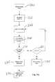
- FIG. 3Agraphically depicts a method or flow helpful in understanding embodiments of the invention.
- threshold parameter Kmay be calculated or preconfigured, as described herein, and pulse counter (N) may be set (or reset) to zero (“0”).
- an erase pulsemay be applied.
- the pulse counter Nmay be incremented to reflect the current number of pulses applied.
- the memory componentmay be examined to determine whether data in all cells included in the memory component has been erased. It will be recognized that an erase operation may typically include programming all cells to some high program level, and then applying one or more erase pulses. Accordingly, cells that are not yet erased may refer to cells corresponding to a voltage threshold above the erase level.
- the current number of pulses Nmay be compared to a threshold parameter K, which may be dynamically set or may be preconfigured.
- Ka threshold parameter
- the processmay be terminated. Any result or parameter may be stored. Any information stored, may be used, e.g., in a subsequent or current erase operation.
- the method or flowmay repeat the operations described with respect to blocks 265 , 270 and 275 . Accordingly, the number of pulses applied in the current erase operation may be stored in the counter N.
- a processmay proceed to operation 290 .
- the number of P/E cycles applied to the memory componentmay be incremented and recorded.
- monitoring and setting erase parameters based solely on the number of P/E cyclesmay limit system life span in terms of actual P/E cycles.
- embodiments of the inventionmay set erase parameters based on a measure of the overall condition of a memory component to improve system life span in terms of actual P/E cycles (e.g., in FIG. 3B ).
- FIG. 3Bgraphically depicts a method or flow according to embodiments of the invention. It will be noted that methods and/or operations described herein may be applied to any suitable memory component, e.g., a memory block, page, cell or system.
- a data erase operation in a memory componentmay begin.
- threshold parameter Kmay be calculated, as described herein, and pulse counter (N) may be set (or reset) to zero (“0”).
- an erase pulsemay be applied.
- MMU 126may instruct controller 151 to apply an erase pulse.
- the pulse counter Nmay be incremented (e.g., by MMU 126 ) to reflect the current number of pulses applied.
- the memory componentmay be examined to determine whether data in all cells included in the memory component has been erased.
- controller 151may report to MMU 126 the number of cells erased, the number of cells still storing data or any other parameter based on which MMU 126 may determine the number of cells that are not yet erased after an application of an erase pulse as shown by 215 .
- an erase operationmay typically include programming all cells to some high program level, and then applying one or more erase pulses. Accordingly, cells that are not yet erased may refer to cells corresponding to a voltage threshold above the erase level.
- the current number of pulses Nmay be compared to a threshold parameter K, which may be dynamically set or may be preconfigured.
- Kmay be dynamically set or may be preconfigured.
- the processmay be terminated. Any result or parameter may be stored.
- MMU 126may store any information related to memory system 150 on storage 130 . Any information stored, e.g., on storage 130 may be used, e.g., in a subsequent or current erase operation.
- the method or flowmay repeat the operations described with respect to blocks 215 , 220 and 225 . Accordingly, the number of pulses applied in the current erase operation may be stored in the counter N.
- a global or total number of pulses applied to the memory componentmay be calculated by adding the current pulse counter N to a global or total counter M.
- Mmay store the total number of pulses applied to a memory component over days, weeks or years.
- internal controller 151may be instructed to delete data in a memory component, may perform the erase operation and may further report the number of pulses required. In such case, some of the operations described above with respect to FIGS. 3A and 3B may be omitted. In other cases, e.g., if controller 151 is not configured to independently perform an erase operation and/or report the number of pulses required, MMU 126 may instruct controller 151 (or other relevant component) to apply a single pulse and the state of the memory component (e.g., erase status) may be examined after each application of such single pulse.
- MMU 126may instruct controller 151 (or other relevant component) to apply a single pulse and the state of the memory component (e.g., erase status) may be examined after each application of such single pulse.
- the total or global number of pulses applied to a memory componentmay be used to estimate or indicate the true condition of the memory component, e.g., the condition of a memory a block.
- MMU 126may store the number of pulses applied in the current erase process (e.g., the value of N at the end of the process as shown by block 235 ). Accordingly, a change, variance, gradient or other parameter indicating a change of N over time and/or erase processes may be observed, and a condition of the relevant memory component may be determined or estimated. Any operation may be based on such stored information.
- MMU 126may relate the number of pulses required to successfully erase a block of memory (the current N) to the number of pulses required in the previous erase operation (the previous N) and may determine a condition of the memory block by observing the relations between such two values. Any number of parameters related to any number of operations may be stored and used. Accordingly, any computation based on any previous or historical values or parameters may be performed in order to determine a condition of a memory component.
- any number, value or parameter related to an erase process, a P/E cycle or any interaction with a memory componentmay be recorded and/or used to determine a condition of the memory component and/or determine parameters related to an operation related to the memory component.
- the amount of energy required in order to delete data in a memory componentmay be calculated or estimated.
- the amount of energymay be calculated as the product of pulse duration and pulse voltage.
- the sum of energy required to delete data in a memory component(e.g., used in a process as described with respect to FIG. 3B ) may be calculated and recorded.
- MMU 126may set (or internal controller 151 may report to MMU 126 ), values such as pulse duration, pulse voltage levels and/or number of pulses applied, and MMU 126 may, based on such information, compute (and/or record) the total amount of energy applied.
- a condition of a memory componentmay be computed, calculated, derived or determined dynamically, e.g., during an erase process. For example, following an application of one or more erase pulses, the number of non-erased cells (cells still storing data at a given read threshold value) may be determined (e.g., as reported by controller 151 ) and the number of erase pulses applied may be to compute the a condition of a block or other memory component. For example, a table or function that maps a pulse count and number of non-erased cells may be provided to MMU 126 that may use such function or table to calculate a condition parameter based on a pulse count and number of non-erased cells. As described herein, based on one or more condition parameters, future erase parameters, e.g., amount of energy, number of pulses, pulse duration, pulse voltage or any other pulse characteristics may be computed, stored and used in subsequent operations.
- future erase parameterse.g., amount of energy, number of pulses, pulse duration, pulse voltage or any other
- Flash cells in a memory componentare typically not truly identical to each other, due to various reasons, e.g., manufacturing conditions, doping substance impurities, differential temperature or heat, etc. Accordingly, a pulse may delete data in a first cell but fail to delete data in a second cell. In some cases, an erase process may be prolonged due to a few flash cells which are difficult to erase. Accordingly, additional or excess pulses, which may harm the memory component, may be needed in order for all the cells included in a memory block or component to be erased.
- an erase processmay be terminated when a threshold number or percentage of cells are erased and/or when a threshold number, portion or percentage of cells are still storing data.
- ECCerror correction code
- the controllermay store information defining the position of bits which were not properly erased and may use this information later during decoding (e.g., after programming) This information may be used as erasure information.
- erasure informationprovides a new state of a symbol (or a bit) in which the exact polarity of the bit (i.e., ‘0’ or ‘1’) may not be determined This additional information may further reduce the probability of decoding failure.
- Terminating an erase process based on a threshold parametermay increase a flash device's life span (in terms of P/E cycles) as well as shorten an erase process duration.
- the threshold parameter(e.g., the number or percentage of cells to be left non-erased or storing data when the erase process terminates) may be dynamically or otherwise set, tuned or determined
- a condition parametere.g., derived as described herein
- an erase termination thresholdmay be set based on an amount of energy required to delete data in a memory block (e.g., an amount of energy determined as described herein) or a termination threshold may be set based on a total number of pulses already applied to a memory component (e.g., M in FIG. 3B ).
- the erase termination thresholdmay set based on the total number of P/E cycles applied to the memory component or other age parameter.
- an ECCmay be designed to accommodate errors in a relatively “old” memory component (e.g., suited for end-of-life conditions) or a specific condition of the component.
- the thresholdmay be adapted to the age (e.g., an age represented in number of P/E cycles) such that the error rate is always within the capacity of the ECC.
- the erase termination thresholdmay be dynamically lowered based on the total number of P/E cycles applied to a memory component.
- FIG. 4graphically depicts a method or flow according to embodiments of the invention. It will be noted that steps and/or operations in flows or methods described herein may be performed in any order. Some operations may be repeated or omitted. As shown in FIG. 4 , operations shown in blocks 310 , 312 , 315 and 320 may be similar to respective operations 210 , 212 , 215 and 220 shown in FIG. 3B . As shown by block 325 , following an application of an erase pulse, the number of cells that were not erased may be determined For example, controller 151 may report the number of flash cells still storing information following an application of an erase pulse. The number of non-erased cells may be related to a given logical page, block, row or any subset of a block. Any method of determining whether data in cells was deleted may be used, e.g., based on the relevant memory component.
- the number of non-erased cells in a given read threshold valuemay be compared or otherwise related to a threshold E th that may be dynamically or otherwise set.
- E thmay be a percentage or it may be an actual number of cells with V th above 0V.
- E thset based on an age of a memory component, based on the number of P/E cycles already applied to a component, based on a condition of a component (e.g., a condition parameter set or defined as described herein).
- an additional erase pulsemay be applied.
- the number of pulses appliedmay be compared to a threshold (denote by K in FIG. 4 ). As shown by the arrow connecting blocks 330 and 315 , if the number of pulses N has not reached or is not larger than a threshold K, an additional erase pulse may be applied. Although as shown, a single check may include or be related to the number of non-erased cells and the number of pulses applied, some embodiments may apply separate examinations of these aspects. Accordingly, in some embodiments, based on various conditions, additional pulses may be applied even if the number of pulses has reached a predefined limit or even if the number of non-erased cells is below a predefined threshold.
- the erase processmay be terminated and an indication of failure may be generated and/or recorded. Any parameter may be recorded, e.g., the number of pulses applied in the current process, the number of non-erased cells etc.
- block 345if the number of pulses applied is below a first threshold (K) and the number of non-erased cells is below a second threshold (E th ) then it may be determined the process was successful.
- the total number of pulses appliedmay be recorded.
- block 350does not list all parameters that may be recorded upon termination of an erase process, however, it will be understood that any parameter may be recorded. Any parameter, e.g., K, E th , as well as pulse duration, voltage etc. may be determined, e.g., in a subsequent erase process, based on parameters recorded as shown by blocks 350 and 240 .
- any parameter, threshold, count or other valuemay be dynamically set, e.g., during an erase operation.
- parameterssuch as, but not limited to, an erase program voltage, a maximal number of pulses, a pulse duration or an erase voltage step may be set dynamically.
- a resulte.g., the number of non-erased cells
- one or more of the above mentioned parameters or other parametersmay be defined, set or modified.
- parametersmay be set and stored upon a termination of an erase process and used in a subsequent erase process or procedure.
- embodiments of the inventionmay improve utilization of a flash memory component. For example, by applying a number of erase cycles to a memory and dynamically and/or adaptively setting erase parameters between cycles, embodiments of the invention may determine and use an optimal set of erase parameters in an erase operation or procedure. For example, the amount of energy (e.g., as reflected by the number of pulses or relevant pulse characteristics) may be optimal, e.g., no more than the amount of required energy is used.
- an adaptive erase proceduremay include attempting to erase a programmed memory block at the lowest erase voltage and/or the minimal number of erase pulses.
- a proceduremay include determining an erase result, e.g., by a counter provided by an internal counter (e.g., maintained by an internal controller) or by directly attempting to read data from memory cells and determining the number of cells storing data and/or the number of cells on which data was erased. If the number of errors (e.g., number of non-erased cells) exceeds a threshold, then an adaptive erase flow, method or procedure may modify erase parameters based on a result of a previous cycle or operation. For example, erase voltage and/or number of erase pulses and/or erase pulse duration and/or erase voltage step parameters may be modified based on the number of cells in a memory component with respect to which a previous erase cycle or procedure failed to delete data.
- an adaptive erase flow, method or proceduremay modify erase parameters based on a result of a previous cycle or operation. For example, erase voltage and/or number of erase pulses and/or erase pulse duration and/or erase voltage step parameters may be modified based on the number of cells in a memory component with respect to which
- the adaptation of erase parametersmay take place for every set of P/E cycles, and not necessarily for every erase operation. This approach may reduce the complexity involved in optimizing the erase parameters from a controller. Parameter adaptation may involve several erase and read attempts with different parameters, and therefore, once the parameters are set, they may be used by the controller for other memory blocks with the same or similar P/E cycle range.
- FIG. 5graphically depicts a method or flow according to embodiments of the invention. It will be noted that parameters set or modified as shown in FIG. 5 are exemplary ones and that any other applicable parameters, values, thresholds or numbers may be dynamically set during an erase procedure and/or upon a termination of an erase procedure.
- an erase operationmay be initiated, e.g., controller 105 may receive a command to erase data in a memory block included in memory system 150 .
- erase parametersmay be selected. For example and as shown, a voltage level applied to memory cells, the number of pulses applied, the duration or length of pulses applied may be set or selected and a voltage step used to increase the applied voltage may be selected, determined or set.
- an erase commandmay be issued. For example, after setting erase parameters as shown by block 420 , controller may invoke an erase operation based on the erase parameters set as shown in block 420 .
- a result of an erase procedure or operationmay be examined and errors may be identified.
- a counter or other construct or parametere.g., a counter maintained by controller 151
- the countermay be read.
- the number of cells that were not erasednamely, the number of cells storing data after an erase operation may be determined by directly counting cells still storing data or by otherwise examining a memory to determine the number of cells that are not fully erased.
- the number of erase errorse.g., as reflected by the number of non-erased cells may be compared to a threshold parameter.
- erase parametersmay be modified. For example, modification of erase parameters may be based on the number or percentage of cells on which data was successfully erased or deleted. In other embodiments, modification of erase parameters may be based on the number or percentage of cells on which the erase procedure failed to delete data. As shown by the arrow connecting blocks 450 and 420 , following a failure to successfully delete data from all or a portion of cells in a memory, the flow or method may repeat operations such as an erase operation according to modified erase parameters.
- erase parametersmay be modified, e.g., based on an overall result of a number of erase iterations or procedures.
- a condition parametermay be updated as shown by block 455 . For example, based on the voltage level applied, total amount of energy applied (e.g., calculated as the product of pulse voltage and pulse duration), number of pulses etc., a condition parameter may be updated such that the effect of the erase procedure is reflected by the condition parameter. For example, a value of an age parameter reflecting an effective age of a memory system may be increased according to the total amount of energy used in an erase procedure as shown by FIG. 5 .
- Termination of a flowmay include recording any relevant parameters. For example, based on the number of pulses applied, the total energy used and/or other erase parameters, parameters for subsequent or future erase operations may be set. For example, an estimated number of pulses, pulse duration or other erase parameters that may be optimal for a subsequent or future erase operation may be recorded and used in a subsequent operation.
- setting erase parameters as shown by block 420may include setting erase parameters based on erase parameters determined and stored in a previous erase operation, e.g., as shown by block 455 .
Landscapes
- Engineering & Computer Science (AREA)
- Microelectronics & Electronic Packaging (AREA)
- Read Only Memory (AREA)
Abstract
Description
Claims (20)
Priority Applications (1)
| Application Number | Priority Date | Filing Date | Title |
|---|---|---|---|
| US13/238,983US8553468B2 (en) | 2011-09-21 | 2011-09-21 | System and method for managing erase operations in a non-volatile memory |
Applications Claiming Priority (1)
| Application Number | Priority Date | Filing Date | Title |
|---|---|---|---|
| US13/238,983US8553468B2 (en) | 2011-09-21 | 2011-09-21 | System and method for managing erase operations in a non-volatile memory |
Publications (2)
| Publication Number | Publication Date |
|---|---|
| US20130070527A1 US20130070527A1 (en) | 2013-03-21 |
| US8553468B2true US8553468B2 (en) | 2013-10-08 |
Family
ID=47880548
Family Applications (1)
| Application Number | Title | Priority Date | Filing Date |
|---|---|---|---|
| US13/238,983Active2032-04-19US8553468B2 (en) | 2011-09-21 | 2011-09-21 | System and method for managing erase operations in a non-volatile memory |
Country Status (1)
| Country | Link |
|---|---|
| US (1) | US8553468B2 (en) |
Cited By (2)
| Publication number | Priority date | Publication date | Assignee | Title |
|---|---|---|---|---|
| US20130301353A1 (en)* | 2012-05-14 | 2013-11-14 | Samsung Electronics Co., Ltd. | Methods of Driving a Memory |
| US9305657B2 (en) | 2014-02-13 | 2016-04-05 | Samsung Electronics Co., Ltd. | Non-volatile memory device and related method of operation |
Families Citing this family (35)
| Publication number | Priority date | Publication date | Assignee | Title |
|---|---|---|---|---|
| US8762620B2 (en) | 2007-12-27 | 2014-06-24 | Sandisk Enterprise Ip Llc | Multiprocessor storage controller |
| US9699263B1 (en) | 2012-08-17 | 2017-07-04 | Sandisk Technologies Llc. | Automatic read and write acceleration of data accessed by virtual machines |
| US9612948B2 (en) | 2012-12-27 | 2017-04-04 | Sandisk Technologies Llc | Reads and writes between a contiguous data block and noncontiguous sets of logical address blocks in a persistent storage device |
| US9454420B1 (en) | 2012-12-31 | 2016-09-27 | Sandisk Technologies Llc | Method and system of reading threshold voltage equalization |
| US9870830B1 (en) | 2013-03-14 | 2018-01-16 | Sandisk Technologies Llc | Optimal multilevel sensing for reading data from a storage medium |
| US9524235B1 (en) | 2013-07-25 | 2016-12-20 | Sandisk Technologies Llc | Local hash value generation in non-volatile data storage systems |
| US9639463B1 (en) | 2013-08-26 | 2017-05-02 | Sandisk Technologies Llc | Heuristic aware garbage collection scheme in storage systems |
| US9442662B2 (en) | 2013-10-18 | 2016-09-13 | Sandisk Technologies Llc | Device and method for managing die groups |
| US9436831B2 (en) | 2013-10-30 | 2016-09-06 | Sandisk Technologies Llc | Secure erase in a memory device |
| US9703816B2 (en) | 2013-11-19 | 2017-07-11 | Sandisk Technologies Llc | Method and system for forward reference logging in a persistent datastore |
| US9520197B2 (en)* | 2013-11-22 | 2016-12-13 | Sandisk Technologies Llc | Adaptive erase of a storage device |
| US9520162B2 (en) | 2013-11-27 | 2016-12-13 | Sandisk Technologies Llc | DIMM device controller supervisor |
| US9582058B2 (en) | 2013-11-29 | 2017-02-28 | Sandisk Technologies Llc | Power inrush management of storage devices |
| US9703636B2 (en) | 2014-03-01 | 2017-07-11 | Sandisk Technologies Llc | Firmware reversion trigger and control |
| JP2015176628A (en)* | 2014-03-17 | 2015-10-05 | 株式会社東芝 | Semiconductor memory device and memory controller |
| US9448876B2 (en) | 2014-03-19 | 2016-09-20 | Sandisk Technologies Llc | Fault detection and prediction in storage devices |
| US9454448B2 (en) | 2014-03-19 | 2016-09-27 | Sandisk Technologies Llc | Fault testing in storage devices |
| US9626399B2 (en) | 2014-03-31 | 2017-04-18 | Sandisk Technologies Llc | Conditional updates for reducing frequency of data modification operations |
| US9626400B2 (en) | 2014-03-31 | 2017-04-18 | Sandisk Technologies Llc | Compaction of information in tiered data structure |
| US9697267B2 (en) | 2014-04-03 | 2017-07-04 | Sandisk Technologies Llc | Methods and systems for performing efficient snapshots in tiered data structures |
| US10114557B2 (en) | 2014-05-30 | 2018-10-30 | Sandisk Technologies Llc | Identification of hot regions to enhance performance and endurance of a non-volatile storage device |
| US10656842B2 (en) | 2014-05-30 | 2020-05-19 | Sandisk Technologies Llc | Using history of I/O sizes and I/O sequences to trigger coalesced writes in a non-volatile storage device |
| US10146448B2 (en) | 2014-05-30 | 2018-12-04 | Sandisk Technologies Llc | Using history of I/O sequences to trigger cached read ahead in a non-volatile storage device |
| US9703491B2 (en) | 2014-05-30 | 2017-07-11 | Sandisk Technologies Llc | Using history of unaligned writes to cache data and avoid read-modify-writes in a non-volatile storage device |
| US10162748B2 (en) | 2014-05-30 | 2018-12-25 | Sandisk Technologies Llc | Prioritizing garbage collection and block allocation based on I/O history for logical address regions |
| US10372613B2 (en) | 2014-05-30 | 2019-08-06 | Sandisk Technologies Llc | Using sub-region I/O history to cache repeatedly accessed sub-regions in a non-volatile storage device |
| US10656840B2 (en) | 2014-05-30 | 2020-05-19 | Sandisk Technologies Llc | Real-time I/O pattern recognition to enhance performance and endurance of a storage device |
| US9652381B2 (en) | 2014-06-19 | 2017-05-16 | Sandisk Technologies Llc | Sub-block garbage collection |
| US9443601B2 (en) | 2014-09-08 | 2016-09-13 | Sandisk Technologies Llc | Holdup capacitor energy harvesting |
| US9927987B2 (en) | 2015-08-28 | 2018-03-27 | Sandisk Technologies Llc | Adaptive multi-phase erase |
| US9779823B2 (en) | 2016-01-06 | 2017-10-03 | Sandisk Technologies Llc | Secure erase of non-volatile memory |
| KR102643658B1 (en)* | 2016-11-10 | 2024-03-07 | 에스케이하이닉스 주식회사 | Semiconductor memory device and operating method thereof |
| US10628076B1 (en)* | 2018-10-01 | 2020-04-21 | Micron Technology, Inc. | Data erasure in memory sub-systems |
| CN111863091B (en)* | 2019-04-29 | 2022-07-08 | 北京兆易创新科技股份有限公司 | Method and device for controlling erasing performance |
| US11049566B2 (en)* | 2019-07-31 | 2021-06-29 | Micron Technology, Inc. | Erase cycle healing using a high voltage pulse |
Citations (210)
| Publication number | Priority date | Publication date | Assignee | Title |
|---|---|---|---|---|
| US4463375A (en) | 1982-09-07 | 1984-07-31 | The Board Of Trustees Of The Leland Standford Junior University | Multiple-measurement noise-reducing system |
| US4584686A (en) | 1983-12-22 | 1986-04-22 | Optical Storage International | Reed-Solomon error correction apparatus |
| US4589084A (en) | 1983-05-16 | 1986-05-13 | Rca Corporation | Apparatus for symmetrically truncating two's complement binary signals as for use with interleaved quadrature signals |
| US4866716A (en) | 1987-05-15 | 1989-09-12 | Digital Equipment Corporation | Real-time BCH error correction code decoding mechanism |
| US5077737A (en) | 1989-08-18 | 1991-12-31 | Micron Technology, Inc. | Method and apparatus for storing digital data in off-specification dynamic random access memory devices |
| US5297153A (en) | 1989-08-24 | 1994-03-22 | U.S. Philips Corporation | Method and apparatus for decoding code words protected wordwise by a non-binary BCH code from one or more symbol errors |
| US5657332A (en) | 1992-05-20 | 1997-08-12 | Sandisk Corporation | Soft errors handling in EEPROM devices |
| US5729490A (en) | 1995-07-31 | 1998-03-17 | Sgs-Thomson Microelectronics S.R.L. | Parallel-dichotomic serial sensing method for sensing multiple-level non-volatile memory cells, and sensing circuit for actuating such method |
| US5793774A (en) | 1994-11-04 | 1998-08-11 | Fujitsu Limited | Flash memory controlling system |
| US5926409A (en) | 1997-09-05 | 1999-07-20 | Information Storage Devices, Inc. | Method and apparatus for an adaptive ramp amplitude controller in nonvolatile memory application |
| US5956268A (en) | 1997-02-12 | 1999-09-21 | Hyundai Electronics America | Nonvolatile memory structure |
| US5982659A (en) | 1996-12-23 | 1999-11-09 | Lsi Logic Corporation | Memory cell capable of storing more than two logic states by using different via resistances |
| US6038634A (en) | 1998-02-02 | 2000-03-14 | International Business Machines Corporation | Intra-unit block addressing system for memory |
| US6094465A (en) | 1997-03-21 | 2000-07-25 | Qualcomm Incorporated | Method and apparatus for performing decoding of CRC outer concatenated codes |
| US6119245A (en) | 1997-08-06 | 2000-09-12 | Oki Electric Industry Co., Ltd. | Semiconductor storage device and method of controlling it |
| US6182261B1 (en) | 1998-11-05 | 2001-01-30 | Qualcomm Incorporated | Efficient iterative decoding |
| US6192497B1 (en) | 1998-08-27 | 2001-02-20 | Adaptec, Inc. | Parallel Chien search circuit |
| US6195287B1 (en) | 1999-02-03 | 2001-02-27 | Sharp Kabushiki Kaisha | Data programming method for a nonvolatile semiconductor storage |
| US6199188B1 (en) | 1997-10-07 | 2001-03-06 | Quantum Corporation | System for finding roots of degree three and degree four error locator polynomials over GF(2M) |
| US6209114B1 (en) | 1998-05-29 | 2001-03-27 | Texas Instruments Incorporated | Efficient hardware implementation of chien search polynomial reduction in reed-solomon decoding |
| US6259627B1 (en) | 2000-01-27 | 2001-07-10 | Multi Level Memory Technology | Read and write operations using constant row line voltage and variable column line load |
| US6279133B1 (en) | 1997-12-31 | 2001-08-21 | Kawasaki Steel Corporation | Method and apparatus for significantly improving the reliability of multilevel memory architecture |
| US6278633B1 (en) | 1999-11-05 | 2001-08-21 | Multi Level Memory Technology | High bandwidth flash memory that selects programming parameters according to measurements of previous programming operations |
| US6301151B1 (en) | 2000-08-09 | 2001-10-09 | Information Storage Devices, Inc. | Adaptive programming method and apparatus for flash memory analog storage |
| US6370061B1 (en) | 2001-06-19 | 2002-04-09 | Advanced Micro Devices, Inc. | Ceiling test mode to characterize the threshold voltage distribution of over programmed memory cells |
| US6374383B1 (en) | 1999-06-07 | 2002-04-16 | Maxtor Corporation | Determining error locations using error correction codes |
| US20020063774A1 (en) | 2000-11-29 | 2002-05-30 | Hillis William Daniel | Method and apparatus for maintaining eye contact in teleconferencing using reflected images |
| US20020085419A1 (en) | 2001-01-04 | 2002-07-04 | Seok-Cheon Kwon | Nonvolatile semiconductor memory device and data input/output control method thereof |
| US20020154769A1 (en) | 2000-12-07 | 2002-10-24 | Petersen Mette Vesterager | Method of generating pseudo-random numbers in an electronic device, and a method of encrypting and decrypting electronic data |
| US6504891B1 (en) | 1995-07-28 | 2003-01-07 | Micron Technology, Inc. | Timer circuit with programmable decode circuitry |
| US6532556B1 (en) | 2000-01-27 | 2003-03-11 | Multi Level Memory Technology | Data management for multi-bit-per-cell memories |
| US6532169B1 (en) | 2001-06-26 | 2003-03-11 | Cypress Semiconductor Corp. | SONOS latch and application |
| US20030065876A1 (en) | 2001-09-28 | 2003-04-03 | Menahem Lasser | Flash management system using only sequential Write |
| US6553533B2 (en) | 1998-02-05 | 2003-04-22 | International Business Machines Corporation | Method and apparatus for detecting and correcting errors and erasures in product ECC-coded data arrays for DVD and similar storage subsystems |
| US6560747B1 (en) | 1999-11-10 | 2003-05-06 | Maxtor Corporation | Error counting mechanism |
| US20030101404A1 (en) | 2001-11-01 | 2003-05-29 | Lijun Zhao | Inner coding of higher priority data within a digital message |
| US20030105620A1 (en) | 2001-01-29 | 2003-06-05 | Matt Bowen | System, method and article of manufacture for interface constructs in a programming language capable of programming hardware architetures |
| US20030192007A1 (en) | 2001-04-19 | 2003-10-09 | Miller David H. | Code-programmable field-programmable architecturally-systolic Reed-Solomon BCH error correction decoder integrated circuit and error correction decoding method |
| US6637002B1 (en) | 1998-10-21 | 2003-10-21 | Maxtor Corporation | Decoder for error correcting block codes |
| US6639865B2 (en) | 2000-10-25 | 2003-10-28 | Samsung Electronics Co., Ltd. | Memory device, method of accessing the memory device, and reed-solomon decoder including the memory device |
| US20040015771A1 (en) | 2002-07-16 | 2004-01-22 | Menahem Lasser | Error correction for non-volatile memory |
| US20040030971A1 (en) | 1999-06-28 | 2004-02-12 | Kabushiki Kaisha Toshiba | Flash memory |
| US6704902B1 (en) | 1998-09-07 | 2004-03-09 | Sony Corporation | Decoding system for error correction code |
| US6751766B2 (en) | 2002-05-20 | 2004-06-15 | Sandisk Corporation | Increasing the effectiveness of error correction codes and operating multi-level memory systems by using information about the quality of the stored data |
| US6772274B1 (en) | 2000-09-13 | 2004-08-03 | Lexar Media, Inc. | Flash memory system and method implementing LBA to PBA correlation within flash memory array |
| US20040153817A1 (en) | 1996-10-24 | 2004-08-05 | Micron Technologies, Inc. | Apparatus and method for detecting over-programming condition in multistate memory device |
| US20040153722A1 (en) | 2002-12-25 | 2004-08-05 | Heng-Kuan Lee | Error correction code circuit with reduced hardware complexity |
| US6781910B2 (en) | 2002-05-17 | 2004-08-24 | Hewlett-Packard Development Company, L.P. | Small area magnetic memory devices |
| US6792569B2 (en) | 2001-04-24 | 2004-09-14 | International Business Machines Corporation | Root solver and associated method for solving finite field polynomial equations |
| US20040181735A1 (en) | 2003-03-04 | 2004-09-16 | Weizhuang (Wayne) Xin | Decoding a received BCH encoded signal |
| US20050013165A1 (en) | 2003-06-17 | 2005-01-20 | Amir Ban | Flash memories with adaptive reference voltages |
| US20050018482A1 (en) | 2002-09-06 | 2005-01-27 | Raul-Adrian Cemea | Techniques for reducing effects of coupling between storage elements of adjacent rows of memory cells |
| US6873543B2 (en) | 2003-05-30 | 2005-03-29 | Hewlett-Packard Development Company, L.P. | Memory device |
| US20050083735A1 (en) | 2003-10-20 | 2005-04-21 | Jian Chen | Behavior based programming of non-volatile memory |
| US6891768B2 (en) | 2002-11-13 | 2005-05-10 | Hewlett-Packard Development Company, L.P. | Power-saving reading of magnetic memory devices |
| US20050117401A1 (en) | 2002-01-18 | 2005-06-02 | Jian Chen | Techniques of recovering data from memory cells affected by field coupling with adjacent memory cells |
| US20050120265A1 (en) | 2003-12-02 | 2005-06-02 | Pline Steven L. | Data storage system with error correction code and replaceable defective memory |
| US20050128811A1 (en) | 2002-05-23 | 2005-06-16 | Renesas Technology Corp. | Nonvolatile semiconductor memory device capable of uniformly inputting/outputting data |
| US20050138533A1 (en) | 2003-09-29 | 2005-06-23 | Canon Kabushiki Kaisha | Encoding/decoding device using a reed-solomon encoder/decoder |
| US20050144368A1 (en) | 2003-12-30 | 2005-06-30 | Samsung Electronics Co., Ltd. | Address mapping method and mapping information managing method for flash memory, and flash memory using the same |
| US20050144213A1 (en) | 2003-12-29 | 2005-06-30 | Xilinx, Inc. | Mathematical circuit with dynamic rounding |
| US6915477B2 (en) | 2001-12-28 | 2005-07-05 | Lucent Technologies Inc. | Delay sensitive adaptive quality control loop for rate adaptation |
| US6914809B2 (en) | 2003-07-07 | 2005-07-05 | Hewlett-Packard Development Company, L.P. | Memory cell strings |
| US20050172179A1 (en) | 2004-01-29 | 2005-08-04 | Brandenberger Sarah M. | System and method for configuring a solid-state storage device with error correction coding |
| US20050169057A1 (en) | 2004-01-30 | 2005-08-04 | Noboru Shibata | Semiconductor memory device which stores plural data in a cell |
| US20050213393A1 (en) | 2004-03-14 | 2005-09-29 | M-Systems Flash Disk Pioneers, Ltd. | States encoding in multi-bit flash cells for optimizing error rate |
| US6952365B2 (en) | 2002-01-18 | 2005-10-04 | Sandisk Corporation | Reducing the effects of noise in non-volatile memories through multiple reads |
| US6961890B2 (en) | 2001-08-16 | 2005-11-01 | Hewlett-Packard Development Company, L.P. | Dynamic variable-length error correction code |
| US6990012B2 (en) | 2003-10-07 | 2006-01-24 | Hewlett-Packard Development Company, L.P. | Magnetic memory device |
| US6996004B1 (en) | 2003-11-04 | 2006-02-07 | Advanced Micro Devices, Inc. | Minimization of FG-FG coupling in flash memory |
| US6999854B2 (en) | 2004-05-28 | 2006-02-14 | International Business Machines Corporation | Medical infusion pump capable of learning bolus time patterns and providing bolus alerts |
| US7010739B1 (en) | 2002-04-11 | 2006-03-07 | Marvell International Ltd. | Error evaluator for inversionless Berlekamp-Massey algorithm in Reed-Solomon decoders |
| US7012835B2 (en) | 2003-10-03 | 2006-03-14 | Sandisk Corporation | Flash memory data correction and scrub techniques |
| US20060059406A1 (en) | 2004-09-10 | 2006-03-16 | Stmicroelectronics S.R.L. | Memory with embedded error correction codes |
| US20060059409A1 (en) | 2004-09-10 | 2006-03-16 | Hanho Lee | Reed-solomon decoder systems for high speed communication and data storage applications |
| US20060064537A1 (en) | 2004-09-21 | 2006-03-23 | Takashi Oshima | Memory card having a storage cell and method of controlling the same |
| US7038950B1 (en) | 2004-11-05 | 2006-05-02 | Spansion Llc | Multi bit program algorithm |
| US20060101193A1 (en) | 2004-11-08 | 2006-05-11 | M-Systems Flash Disk Pioneers, Ltd. | States encoding in multi-bit flash cells for optimizing error rate |
| US7068539B2 (en) | 2004-01-27 | 2006-06-27 | Sandisk Corporation | Charge packet metering for coarse/fine programming of non-volatile memory |
| US7079436B2 (en) | 2003-09-30 | 2006-07-18 | Hewlett-Packard Development Company, L.P. | Resistive cross point memory |
| US20060203587A1 (en) | 2005-03-11 | 2006-09-14 | Yan Li | Partition of non-volatile memory array to reduce bit line capacitance |
| US20060221692A1 (en) | 2005-04-05 | 2006-10-05 | Jian Chen | Compensating for coupling during read operations on non-volatile memory |
| US20060248434A1 (en) | 2005-04-28 | 2006-11-02 | Micron Technology, Inc. | Non-systematic coded error correction |
| US20060268608A1 (en) | 2003-04-22 | 2006-11-30 | Kabushiki Kaisha Toshiba | Data storage system |
| US7149950B2 (en) | 2003-09-12 | 2006-12-12 | Hewlett-Packard Development Company, L.P. | Assisted memory device for reading and writing single and multiple units of data |
| US20060294312A1 (en) | 2004-05-27 | 2006-12-28 | Silverbrook Research Pty Ltd | Generation sequences |
| US20070025157A1 (en) | 2005-08-01 | 2007-02-01 | Jun Wan | Method for programming non-volatile memory with self-adjusting maximum program loop |
| US7177977B2 (en) | 2004-03-19 | 2007-02-13 | Sandisk Corporation | Operating non-volatile memory without read disturb limitations |
| US7191379B2 (en) | 2003-09-10 | 2007-03-13 | Hewlett-Packard Development Company, L.P. | Magnetic memory with error correction coding |
| US20070063180A1 (en) | 2005-09-07 | 2007-03-22 | Elpida Memory, Inc. | Electrically rewritable non-volatile memory element and method of manufacturing the same |
| US7196946B2 (en) | 2005-04-05 | 2007-03-27 | Sandisk Corporation | Compensating for coupling in non-volatile storage |
| US7203874B2 (en) | 2003-05-08 | 2007-04-10 | Micron Technology, Inc. | Error detection, documentation, and correction in a flash memory device |
| US20070104004A1 (en) | 1997-09-08 | 2007-05-10 | So Hock C | Multi-Bit-Per-Cell Flash EEprom Memory with Refresh |
| US20070103992A1 (en) | 2005-11-10 | 2007-05-10 | Sony Corporation | Memory system |
| US20070109858A1 (en) | 2000-12-28 | 2007-05-17 | Conley Kevin M | Novel Method and Structure for Efficient Data Verification Operation for Non-Volatile Memories |
| US20070124652A1 (en) | 2005-11-15 | 2007-05-31 | Ramot At Tel Aviv University Ltd. | Method and device for multi phase error-correction |
| US20070143561A1 (en) | 2005-12-21 | 2007-06-21 | Gorobets Sergey A | Methods for adaptive file data handling in non-volatile memories with a directly mapped file storage system |
| US20070150694A1 (en) | 2003-10-01 | 2007-06-28 | Sandisk Corporation | Hybrid Mapping Implementation Within a Non-Volatile Memory System |
| US20070168625A1 (en) | 2006-01-18 | 2007-07-19 | Cornwell Michael J | Interleaving policies for flash memory |
| US20070171714A1 (en) | 2006-01-20 | 2007-07-26 | Marvell International Ltd. | Flash memory with coding and signal processing |
| US20070171730A1 (en) | 2006-01-20 | 2007-07-26 | Marvell International Ltd. | Method and system for error correction in flash memory |
| US20070180346A1 (en) | 2006-01-18 | 2007-08-02 | Sandisk Il Ltd. | Method Of Arranging Data In A Multi-Level Cell Memory Device |
| US20070226592A1 (en) | 2006-03-20 | 2007-09-27 | Micron Technology, Inc. | Variable sector-count ECC |
| US20070226582A1 (en) | 2006-03-08 | 2007-09-27 | Marvell International Ltd. | Systems and methods for achieving higher coding rate using parity interleaving |
| US20070228449A1 (en) | 2006-03-31 | 2007-10-04 | Tamae Takano | Nonvolatile semiconductor memory device |
| US7290203B2 (en) | 2004-10-29 | 2007-10-30 | International Business Machines Corporation | Dynamic memory architecture employing passive expiration of data |
| US20070253249A1 (en) | 2006-04-26 | 2007-11-01 | Sang-Gu Kang | Multi-bit nonvolatile memory device and related programming method |
| US7292365B2 (en) | 2003-01-15 | 2007-11-06 | Xerox Corporation | Methods and systems for determining distribution mean level without histogram measurement |
| US20070266291A1 (en) | 2006-05-15 | 2007-11-15 | Kabushiki Kaisha Toshiba | Semiconductor memory device |
| US20070263439A1 (en) | 2006-05-15 | 2007-11-15 | Apple Inc. | Dynamic Cell Bit Resolution |
| US20070271494A1 (en) | 2006-05-17 | 2007-11-22 | Sandisk Corporation | Error Correction Coding for Multiple-Sector Pages in Flash Memory Devices |
| US7301928B2 (en) | 2004-06-09 | 2007-11-27 | Hitachi Kokusai Electric Inc. | Wireless packet transfer apparatus and method |
| US20080010581A1 (en) | 2006-07-04 | 2008-01-10 | Ramot At Tel Aviv University Ltd. | Method of error correction in a multi-bit-per-cell flash memory |
| US20080028014A1 (en) | 2006-07-26 | 2008-01-31 | Hilt Jason W | N-BIT 2's COMPLEMENT SYMMETRIC ROUNDING METHOD AND LOGIC FOR IMPLEMENTING THE SAME |
| US20080055989A1 (en) | 2006-09-06 | 2008-03-06 | Kyoong-Han Lee | Memory system including flash memory and method of operating the same |
| US20080082897A1 (en) | 2006-09-28 | 2008-04-03 | Yigal Brandman | Soft-Input Soft-Output Decoder for Nonvolatile Memory |
| US20080092026A1 (en) | 2006-09-28 | 2008-04-17 | Yigal Brandman | Methods of Soft-Input Soft-Output Decoding for Nonvolatile Memory |
| US20080104309A1 (en) | 2006-10-30 | 2008-05-01 | Cheon Won-Moon | Flash memory device with multi-level cells and method of writing data therein |
| US20080116509A1 (en) | 2001-10-31 | 2008-05-22 | Eliyahou Harari | Multi-State Non-Volatile Integrated Circuit Memory Systems that Employ Dielectric Storage Elements |
| US20080127104A1 (en) | 2006-11-27 | 2008-05-29 | Yan Li | Apparatus with segemented bitscan for verification of programming |
| US20080126686A1 (en) | 2006-11-28 | 2008-05-29 | Anobit Technologies Ltd. | Memory power and performance management |
| US20080128790A1 (en) | 2006-11-30 | 2008-06-05 | Jin-Hyo Jung | Memory device |
| US20080130341A1 (en) | 2006-12-03 | 2008-06-05 | Anobit Technologies Ltd. | Adaptive programming of analog memory |
| US20080137413A1 (en) | 2006-12-06 | 2008-06-12 | Samsung Electronics Co., Ltd | Multi-level cell memory devices using trellis coded modulation and methods of storing data in and reading data from the memory devices |
| US20080148115A1 (en) | 2006-12-17 | 2008-06-19 | Anobit Technologies Ltd. | High-speed programming of memory devices |
| US20080159059A1 (en) | 2007-01-03 | 2008-07-03 | Freescale Semiconductor, Inc. | Progressive memory initialization with waitpoints |
| US20080162079A1 (en) | 2006-10-05 | 2008-07-03 | International Business Machines Corp. | End of life prediction of flash memory |
| US20080158958A1 (en) | 2006-12-17 | 2008-07-03 | Anobit Technologies Ltd. | Memory device with reduced reading |
| US20080168216A1 (en) | 2007-01-09 | 2008-07-10 | Lee Seung-Jae | Memory system, multi-bit flash memory device, and associated methods |
| US20080168320A1 (en) | 2007-01-05 | 2008-07-10 | California Institute Of Technology | Codes For Limited Magnitude Asymetric Errors In Flash Memories |
| US20080181001A1 (en) | 2007-01-24 | 2008-07-31 | Anobit Technologies | Memory device with negative thresholds |
| US20080198650A1 (en) | 2006-05-12 | 2008-08-21 | Anobit Technologies Ltd. | Distortion Estimation And Cancellation In Memory Devices |
| US20080198652A1 (en) | 2006-05-12 | 2008-08-21 | Anobit Technologies Ltd. | Memory Device Programming Using Combined Shaping And Linear Spreading |
| US20080219050A1 (en) | 2007-01-24 | 2008-09-11 | Anobit Technologies Ltd. | Reduction of back pattern dependency effects in memory devices |
| US20080225599A1 (en) | 2007-03-15 | 2008-09-18 | Samsung Electronics Co., Ltd. | Flash memory device with reduced coupling effect among cells and method of driving the same |
| US7441067B2 (en) | 2004-11-15 | 2008-10-21 | Sandisk Corporation | Cyclic flash memory wear leveling |
| US20080263262A1 (en) | 2007-04-22 | 2008-10-23 | Anobit Technologies Ltd. | Command interface for memory devices |
| US20080282106A1 (en) | 2007-05-12 | 2008-11-13 | Anobit Technologies Ltd | Data storage with incremental redundancy |
| US20080285351A1 (en) | 2007-05-14 | 2008-11-20 | Mark Shlick | Measuring threshold voltage distribution in memory using an aggregate characteristic |
| US20080301532A1 (en) | 2006-09-25 | 2008-12-04 | Kabushiki Kaisha Toshiba | Non-volatile semiconductor memory device |
| US20090024905A1 (en) | 2006-05-12 | 2009-01-22 | Anobit Technologies Ltd. | Combined distortion estimation and error correction coding for memory devices |
| US20090043951A1 (en) | 2007-08-06 | 2009-02-12 | Anobit Technologies Ltd. | Programming schemes for multi-level analog memory cells |
| US20090072303A9 (en) | 2002-06-21 | 2009-03-19 | Micron Technology, Inc. | Nrom memory cell, memory array, related devices and methods |
| US20090091979A1 (en) | 2007-10-08 | 2009-04-09 | Anobit Technologies | Reliable data storage in analog memory cells in the presence of temperature variations |
| US20090103358A1 (en) | 2006-05-12 | 2009-04-23 | Anobit Technologies Ltd. | Reducing programming error in memory devices |
| US20090106485A1 (en) | 2007-10-19 | 2009-04-23 | Anobit Technologies Ltd. | Reading analog memory cells using built-in multi-threshold commands |
| US20090113275A1 (en) | 2007-10-29 | 2009-04-30 | Legend Silicon Corp. | Bch code with 256 information bytes and up to 8 bytes of parity check elements |
| US20090125671A1 (en) | 2006-12-06 | 2009-05-14 | David Flynn | Apparatus, system, and method for storage space recovery after reaching a read count limit |
| US20090144600A1 (en) | 2007-11-30 | 2009-06-04 | Anobit Technologies Ltd | Efficient re-read operations from memory devices |
| US20090150748A1 (en) | 2004-08-02 | 2009-06-11 | Koninklijke Philips Electronics N.V. | Data Storage and Replay Apparatus |
| US20090157964A1 (en) | 2007-12-16 | 2009-06-18 | Anobit Technologies Ltd. | Efficient data storage in multi-plane memory devices |
| US20090158126A1 (en) | 2007-12-12 | 2009-06-18 | Anobit Technologies Ltd | Efficient interference cancellation in analog memory cell arrays |
| US20090168524A1 (en) | 2007-12-27 | 2009-07-02 | Anobit Technologies Ltd. | Wear level estimation in analog memory cells |
| US7558109B2 (en) | 2006-11-03 | 2009-07-07 | Sandisk Corporation | Nonvolatile memory with variable read threshold |
| US20090187803A1 (en) | 2008-01-21 | 2009-07-23 | Anobit Technologies Ltd. | Decoding of error correction code using partial bit inversion |
| US20090199074A1 (en) | 2008-02-05 | 2009-08-06 | Anobit Technologies Ltd. | Parameter estimation based on error correction code parity check equations |
| US20090213653A1 (en) | 2008-02-21 | 2009-08-27 | Anobit Technologies Ltd | Programming of analog memory cells using a single programming pulse per state transition |
| US20090213654A1 (en) | 2008-02-24 | 2009-08-27 | Anobit Technologies Ltd | Programming analog memory cells for reduced variance after retention |
| US20090228761A1 (en) | 2008-03-07 | 2009-09-10 | Anobit Technologies Ltd | Efficient readout from analog memory cells using data compression |
| US20090240872A1 (en) | 2008-03-18 | 2009-09-24 | Anobit Technologies Ltd | Memory device with multiple-accuracy read commands |
| US20100005270A1 (en) | 2008-03-07 | 2010-01-07 | Via Technologies, Inc. | Storage unit management methods and systems |
| US20100058146A1 (en) | 2007-12-12 | 2010-03-04 | Hanan Weingarten | Chien-search system employing a clock-gating scheme to save power for error correction decoder and other applications |
| US20100064096A1 (en) | 2007-12-05 | 2010-03-11 | Hanan Weingarten | Systems and methods for temporarily retiring memory portions |
| US20100088557A1 (en) | 2007-10-25 | 2010-04-08 | Hanan Weingarten | Systems and methods for multiple coding rates in flash devices |
| US20100091535A1 (en) | 2007-03-12 | 2010-04-15 | Anobit Technologies Ltd | Adaptive estimation of memory cell read thresholds |
| US20100095186A1 (en) | 2008-08-20 | 2010-04-15 | Hanan Weingarten | Reprogramming non volatile memory portions |
| US20100110787A1 (en) | 2006-10-30 | 2010-05-06 | Anobit Technologies Ltd. | Memory cell readout using successive approximation |
| US20100115376A1 (en) | 2006-12-03 | 2010-05-06 | Anobit Technologies Ltd. | Automatic defect management in memory devices |
| US20100122113A1 (en) | 2007-09-20 | 2010-05-13 | Hanan Weingarten | Systems and methods for handling immediate data errors in flash memory |
| US20100124088A1 (en) | 2008-11-16 | 2010-05-20 | Anobit Technologies Ltd | Storage at m bits/cell density in n bits/cell analog memory cell devices, m>n |
| US20100131806A1 (en) | 2007-12-18 | 2010-05-27 | Hanan Weingarten | Apparatus for coding at a plurality of rates in multi-level flash memory systems, and methods useful in conjunction therewith |
| US20100131580A1 (en) | 2008-03-25 | 2010-05-27 | Densbits Technologies Ltd. | Apparatus and methods for hardware-efficient unbiased rounding |
| US20100131827A1 (en) | 2007-05-12 | 2010-05-27 | Anobit Technologies Ltd | Memory device with internal signap processing unit |
| US20100131831A1 (en) | 2007-12-05 | 2010-05-27 | Hanan Weingarten | low power chien-search based bch/rs decoding system for flash memory, mobile communications devices and other applications |
| US20100131826A1 (en) | 2006-08-27 | 2010-05-27 | Anobit Technologies Ltd. | Estimation of non-linear distortion in memory devices |
| US20100146192A1 (en) | 2007-10-22 | 2010-06-10 | Hanan Weingarten | Methods for adaptively programming flash memory devices and flash memory systems incorporating same |
| US20100149881A1 (en) | 2008-12-11 | 2010-06-17 | Shih-Chung Lee | Adaptive erase and soft programming for memory |
| US20100199149A1 (en) | 2007-12-05 | 2010-08-05 | Hanan Weingarten | Flash memory apparatus and methods using a plurality of decoding stages including optional use of concatenated bch codes and/or designation of "first below" cells |
| US20100211724A1 (en) | 2007-09-20 | 2010-08-19 | Hanan Weingarten | Systems and methods for determining logical values of coupled flash memory cells |
| US20100211856A1 (en) | 2007-12-12 | 2010-08-19 | Hanan Weingarten | Systems and methods for error correction and decoding on multi-level physical media |
| US20100211833A1 (en) | 2007-10-22 | 2010-08-19 | Hanan Weingarten | Systems and methods for averaging error rates in non-volatile devices and storage systems |
| US7805664B1 (en) | 2006-10-05 | 2010-09-28 | Marvell International Ltd | Likelihood metric generation for trellis-based detection and/or decoding |
| US7804718B2 (en) | 2007-03-07 | 2010-09-28 | Mosaid Technologies Incorporated | Partial block erase architecture for flash memory |
| US7805663B2 (en) | 2006-09-28 | 2010-09-28 | Sandisk Corporation | Methods of adapting operation of nonvolatile memory |
| US20100251066A1 (en) | 2006-08-31 | 2010-09-30 | Micron Technology, Inc. | Data handling |
| US20100253555A1 (en) | 2009-04-06 | 2010-10-07 | Hanan Weingarten | Encoding method and system, decoding method and system |
| US20100257309A1 (en) | 2009-04-06 | 2010-10-07 | Boris Barsky | Device and method for managing a flash memory |
| US20100293321A1 (en) | 2009-05-12 | 2010-11-18 | Hanan Weingarten | Systems and method for flash memory management |
| US20110055461A1 (en) | 2009-08-26 | 2011-03-03 | Steiner Avi | Systems and methods for pre-equalization and code design for a flash memory |
| US20110051521A1 (en) | 2009-08-26 | 2011-03-03 | Shmuel Levy | Flash memory module and method for programming a page of flash memory cells |
| US7916543B2 (en)* | 2007-10-22 | 2011-03-29 | Micron Technology, Inc. | Memory cell operation |
| US20110096612A1 (en) | 2009-10-22 | 2011-04-28 | Steiner Avi | Method, system, and computer readable medium for reading and programming flash memory cells |
| US20110119562A1 (en) | 2009-11-19 | 2011-05-19 | Steiner Avi | System and method for uncoded bit error rate equalization via interleaving |
| US7961797B1 (en) | 2006-10-10 | 2011-06-14 | Marvell International Ltd. | Nonlinear viterbi complexity reduction |
| US20110153919A1 (en) | 2009-12-22 | 2011-06-23 | Erez Sabbag | Device, system, and method for reducing program/read disturb in flash arrays |
| US20110161775A1 (en) | 2009-12-24 | 2011-06-30 | Hanan Weingarten | System and method for setting a flash memory cell read threshold |
| US20110214039A1 (en) | 2010-02-28 | 2011-09-01 | Steiner Avi | System and method for multi-dimensional decoding |
| US20110246852A1 (en) | 2010-04-06 | 2011-10-06 | Erez Sabbag | System and method for restoring damaged data programmed on a flash device |
| US20110246792A1 (en) | 2010-04-06 | 2011-10-06 | Hanan Weingarten | Method, system and medium for analog encryption in a flash memory |
| US20110252187A1 (en) | 2010-04-07 | 2011-10-13 | Avigdor Segal | System and method for operating a non-volatile memory including a portion operating as a single-level cell memory and a portion operating as a multi-level cell memory |
| US20110252188A1 (en) | 2010-04-07 | 2011-10-13 | Hanan Weingarten | System and method for storing information in a multi-level cell memory |
| US20110271043A1 (en) | 2010-04-29 | 2011-11-03 | Avigdor Segal | System and method for allocating and using spare blocks in a flash memory |
| US20120005558A1 (en) | 2010-07-01 | 2012-01-05 | Steiner Avi | System and method for data recovery in multi-level cell memories |
| US20120005560A1 (en) | 2010-07-01 | 2012-01-05 | Steiner Avi | System and method for multi-dimensional encoding and decoding |
| US20120008401A1 (en) | 2010-07-06 | 2012-01-12 | Michael Katz | Systems and methods for storing, retrieving, and adjusting read thresholds in flash memory storage system |
| US8122328B2 (en) | 2007-03-30 | 2012-02-21 | Samsung Electronics Co., Ltd. | Bose-Chaudhuri-Hocquenghem error correction method and circuit for checking error using error correction encoder |
| US20120051144A1 (en) | 2010-08-24 | 2012-03-01 | Hanan Weingarten | System and method for accelerated sampling |
| US20120063227A1 (en) | 2010-09-15 | 2012-03-15 | Hanan Weingarten | System and method for adjusting read voltage thresholds in memories |
| US20120066441A1 (en) | 2009-10-15 | 2012-03-15 | Densbits Technologies Ltd. | Systems and methods for averaging error rates in non-volatile devices and storage systems |
| US20120110250A1 (en) | 2010-11-03 | 2012-05-03 | Densbits Technologies Ltd. | Meethod, system and computer readable medium for copy back |
- 2011
- 2011-09-21USUS13/238,983patent/US8553468B2/enactiveActive
Patent Citations (229)
| Publication number | Priority date | Publication date | Assignee | Title |
|---|---|---|---|---|
| US4463375A (en) | 1982-09-07 | 1984-07-31 | The Board Of Trustees Of The Leland Standford Junior University | Multiple-measurement noise-reducing system |
| US4589084A (en) | 1983-05-16 | 1986-05-13 | Rca Corporation | Apparatus for symmetrically truncating two's complement binary signals as for use with interleaved quadrature signals |
| US4584686A (en) | 1983-12-22 | 1986-04-22 | Optical Storage International | Reed-Solomon error correction apparatus |
| US4866716A (en) | 1987-05-15 | 1989-09-12 | Digital Equipment Corporation | Real-time BCH error correction code decoding mechanism |
| US5077737A (en) | 1989-08-18 | 1991-12-31 | Micron Technology, Inc. | Method and apparatus for storing digital data in off-specification dynamic random access memory devices |
| US5297153A (en) | 1989-08-24 | 1994-03-22 | U.S. Philips Corporation | Method and apparatus for decoding code words protected wordwise by a non-binary BCH code from one or more symbol errors |
| US5657332A (en) | 1992-05-20 | 1997-08-12 | Sandisk Corporation | Soft errors handling in EEPROM devices |
| US5793774A (en) | 1994-11-04 | 1998-08-11 | Fujitsu Limited | Flash memory controlling system |
| US6504891B1 (en) | 1995-07-28 | 2003-01-07 | Micron Technology, Inc. | Timer circuit with programmable decode circuitry |
| US5729490A (en) | 1995-07-31 | 1998-03-17 | Sgs-Thomson Microelectronics S.R.L. | Parallel-dichotomic serial sensing method for sensing multiple-level non-volatile memory cells, and sensing circuit for actuating such method |
| US20040153817A1 (en) | 1996-10-24 | 2004-08-05 | Micron Technologies, Inc. | Apparatus and method for detecting over-programming condition in multistate memory device |
| US5982659A (en) | 1996-12-23 | 1999-11-09 | Lsi Logic Corporation | Memory cell capable of storing more than two logic states by using different via resistances |
| US5956268A (en) | 1997-02-12 | 1999-09-21 | Hyundai Electronics America | Nonvolatile memory structure |
| US6094465A (en) | 1997-03-21 | 2000-07-25 | Qualcomm Incorporated | Method and apparatus for performing decoding of CRC outer concatenated codes |
| US6119245A (en) | 1997-08-06 | 2000-09-12 | Oki Electric Industry Co., Ltd. | Semiconductor storage device and method of controlling it |
| US5926409A (en) | 1997-09-05 | 1999-07-20 | Information Storage Devices, Inc. | Method and apparatus for an adaptive ramp amplitude controller in nonvolatile memory application |
| US20070104004A1 (en) | 1997-09-08 | 2007-05-10 | So Hock C | Multi-Bit-Per-Cell Flash EEprom Memory with Refresh |
| US6199188B1 (en) | 1997-10-07 | 2001-03-06 | Quantum Corporation | System for finding roots of degree three and degree four error locator polynomials over GF(2M) |
| US6279133B1 (en) | 1997-12-31 | 2001-08-21 | Kawasaki Steel Corporation | Method and apparatus for significantly improving the reliability of multilevel memory architecture |
| US6038634A (en) | 1998-02-02 | 2000-03-14 | International Business Machines Corporation | Intra-unit block addressing system for memory |
| US6553533B2 (en) | 1998-02-05 | 2003-04-22 | International Business Machines Corporation | Method and apparatus for detecting and correcting errors and erasures in product ECC-coded data arrays for DVD and similar storage subsystems |
| US6209114B1 (en) | 1998-05-29 | 2001-03-27 | Texas Instruments Incorporated | Efficient hardware implementation of chien search polynomial reduction in reed-solomon decoding |
| US6192497B1 (en) | 1998-08-27 | 2001-02-20 | Adaptec, Inc. | Parallel Chien search circuit |
| US6704902B1 (en) | 1998-09-07 | 2004-03-09 | Sony Corporation | Decoding system for error correction code |
| US6637002B1 (en) | 1998-10-21 | 2003-10-21 | Maxtor Corporation | Decoder for error correcting block codes |
| US6182261B1 (en) | 1998-11-05 | 2001-01-30 | Qualcomm Incorporated | Efficient iterative decoding |
| US6195287B1 (en) | 1999-02-03 | 2001-02-27 | Sharp Kabushiki Kaisha | Data programming method for a nonvolatile semiconductor storage |
| US6374383B1 (en) | 1999-06-07 | 2002-04-16 | Maxtor Corporation | Determining error locations using error correction codes |
| US20040030971A1 (en) | 1999-06-28 | 2004-02-12 | Kabushiki Kaisha Toshiba | Flash memory |
| US20070223277A1 (en) | 1999-06-28 | 2007-09-27 | Kabushiki Kaisha Toshiba | Flash memory |
| US6278633B1 (en) | 1999-11-05 | 2001-08-21 | Multi Level Memory Technology | High bandwidth flash memory that selects programming parameters according to measurements of previous programming operations |
| US6560747B1 (en) | 1999-11-10 | 2003-05-06 | Maxtor Corporation | Error counting mechanism |
| US6532556B1 (en) | 2000-01-27 | 2003-03-11 | Multi Level Memory Technology | Data management for multi-bit-per-cell memories |
| US6259627B1 (en) | 2000-01-27 | 2001-07-10 | Multi Level Memory Technology | Read and write operations using constant row line voltage and variable column line load |
| US6301151B1 (en) | 2000-08-09 | 2001-10-09 | Information Storage Devices, Inc. | Adaptive programming method and apparatus for flash memory analog storage |
| US6772274B1 (en) | 2000-09-13 | 2004-08-03 | Lexar Media, Inc. | Flash memory system and method implementing LBA to PBA correlation within flash memory array |
| US6639865B2 (en) | 2000-10-25 | 2003-10-28 | Samsung Electronics Co., Ltd. | Memory device, method of accessing the memory device, and reed-solomon decoder including the memory device |
| US20020063774A1 (en) | 2000-11-29 | 2002-05-30 | Hillis William Daniel | Method and apparatus for maintaining eye contact in teleconferencing using reflected images |
| US20020154769A1 (en) | 2000-12-07 | 2002-10-24 | Petersen Mette Vesterager | Method of generating pseudo-random numbers in an electronic device, and a method of encrypting and decrypting electronic data |
| US20070109858A1 (en) | 2000-12-28 | 2007-05-17 | Conley Kevin M | Novel Method and Structure for Efficient Data Verification Operation for Non-Volatile Memories |
| US20020085419A1 (en) | 2001-01-04 | 2002-07-04 | Seok-Cheon Kwon | Nonvolatile semiconductor memory device and data input/output control method thereof |
| US20030105620A1 (en) | 2001-01-29 | 2003-06-05 | Matt Bowen | System, method and article of manufacture for interface constructs in a programming language capable of programming hardware architetures |
| US20030192007A1 (en) | 2001-04-19 | 2003-10-09 | Miller David H. | Code-programmable field-programmable architecturally-systolic Reed-Solomon BCH error correction decoder integrated circuit and error correction decoding method |
| US6792569B2 (en) | 2001-04-24 | 2004-09-14 | International Business Machines Corporation | Root solver and associated method for solving finite field polynomial equations |
| US6370061B1 (en) | 2001-06-19 | 2002-04-09 | Advanced Micro Devices, Inc. | Ceiling test mode to characterize the threshold voltage distribution of over programmed memory cells |
| US6532169B1 (en) | 2001-06-26 | 2003-03-11 | Cypress Semiconductor Corp. | SONOS latch and application |
| US6674665B1 (en) | 2001-06-26 | 2004-01-06 | Cypress Semiconductor Corp. | SONOS latch and application |
| US6961890B2 (en) | 2001-08-16 | 2005-11-01 | Hewlett-Packard Development Company, L.P. | Dynamic variable-length error correction code |
| US20030065876A1 (en) | 2001-09-28 | 2003-04-03 | Menahem Lasser | Flash management system using only sequential Write |
| US20080116509A1 (en) | 2001-10-31 | 2008-05-22 | Eliyahou Harari | Multi-State Non-Volatile Integrated Circuit Memory Systems that Employ Dielectric Storage Elements |
| US20030101404A1 (en) | 2001-11-01 | 2003-05-29 | Lijun Zhao | Inner coding of higher priority data within a digital message |
| US6915477B2 (en) | 2001-12-28 | 2005-07-05 | Lucent Technologies Inc. | Delay sensitive adaptive quality control loop for rate adaptation |
| US20050117401A1 (en) | 2002-01-18 | 2005-06-02 | Jian Chen | Techniques of recovering data from memory cells affected by field coupling with adjacent memory cells |
| US6952365B2 (en) | 2002-01-18 | 2005-10-04 | Sandisk Corporation | Reducing the effects of noise in non-volatile memories through multiple reads |
| US7010739B1 (en) | 2002-04-11 | 2006-03-07 | Marvell International Ltd. | Error evaluator for inversionless Berlekamp-Massey algorithm in Reed-Solomon decoders |
| US6781910B2 (en) | 2002-05-17 | 2004-08-24 | Hewlett-Packard Development Company, L.P. | Small area magnetic memory devices |
| US6751766B2 (en) | 2002-05-20 | 2004-06-15 | Sandisk Corporation | Increasing the effectiveness of error correction codes and operating multi-level memory systems by using information about the quality of the stored data |
| US20050128811A1 (en) | 2002-05-23 | 2005-06-16 | Renesas Technology Corp. | Nonvolatile semiconductor memory device capable of uniformly inputting/outputting data |
| US20090072303A9 (en) | 2002-06-21 | 2009-03-19 | Micron Technology, Inc. | Nrom memory cell, memory array, related devices and methods |
| US20040015771A1 (en) | 2002-07-16 | 2004-01-22 | Menahem Lasser | Error correction for non-volatile memory |
| US20050018482A1 (en) | 2002-09-06 | 2005-01-27 | Raul-Adrian Cemea | Techniques for reducing effects of coupling between storage elements of adjacent rows of memory cells |
| US6891768B2 (en) | 2002-11-13 | 2005-05-10 | Hewlett-Packard Development Company, L.P. | Power-saving reading of magnetic memory devices |
| US20040153722A1 (en) | 2002-12-25 | 2004-08-05 | Heng-Kuan Lee | Error correction code circuit with reduced hardware complexity |
| US7292365B2 (en) | 2003-01-15 | 2007-11-06 | Xerox Corporation | Methods and systems for determining distribution mean level without histogram measurement |
| US20040181735A1 (en) | 2003-03-04 | 2004-09-16 | Weizhuang (Wayne) Xin | Decoding a received BCH encoded signal |
| US20060268608A1 (en) | 2003-04-22 | 2006-11-30 | Kabushiki Kaisha Toshiba | Data storage system |
| US7203874B2 (en) | 2003-05-08 | 2007-04-10 | Micron Technology, Inc. | Error detection, documentation, and correction in a flash memory device |
| US6873543B2 (en) | 2003-05-30 | 2005-03-29 | Hewlett-Packard Development Company, L.P. | Memory device |
| US20050013165A1 (en) | 2003-06-17 | 2005-01-20 | Amir Ban | Flash memories with adaptive reference voltages |
| US6914809B2 (en) | 2003-07-07 | 2005-07-05 | Hewlett-Packard Development Company, L.P. | Memory cell strings |
| US7191379B2 (en) | 2003-09-10 | 2007-03-13 | Hewlett-Packard Development Company, L.P. | Magnetic memory with error correction coding |
| US7149950B2 (en) | 2003-09-12 | 2006-12-12 | Hewlett-Packard Development Company, L.P. | Assisted memory device for reading and writing single and multiple units of data |
| US20050138533A1 (en) | 2003-09-29 | 2005-06-23 | Canon Kabushiki Kaisha | Encoding/decoding device using a reed-solomon encoder/decoder |
| US7079436B2 (en) | 2003-09-30 | 2006-07-18 | Hewlett-Packard Development Company, L.P. | Resistive cross point memory |
| US20070150694A1 (en) | 2003-10-01 | 2007-06-28 | Sandisk Corporation | Hybrid Mapping Implementation Within a Non-Volatile Memory System |
| US7012835B2 (en) | 2003-10-03 | 2006-03-14 | Sandisk Corporation | Flash memory data correction and scrub techniques |
| US6990012B2 (en) | 2003-10-07 | 2006-01-24 | Hewlett-Packard Development Company, L.P. | Magnetic memory device |
| US20050083735A1 (en) | 2003-10-20 | 2005-04-21 | Jian Chen | Behavior based programming of non-volatile memory |
| US6996004B1 (en) | 2003-11-04 | 2006-02-07 | Advanced Micro Devices, Inc. | Minimization of FG-FG coupling in flash memory |
| US20050120265A1 (en) | 2003-12-02 | 2005-06-02 | Pline Steven L. | Data storage system with error correction code and replaceable defective memory |
| US20050144213A1 (en) | 2003-12-29 | 2005-06-30 | Xilinx, Inc. | Mathematical circuit with dynamic rounding |
| US20050144368A1 (en) | 2003-12-30 | 2005-06-30 | Samsung Electronics Co., Ltd. | Address mapping method and mapping information managing method for flash memory, and flash memory using the same |
| US7068539B2 (en) | 2004-01-27 | 2006-06-27 | Sandisk Corporation | Charge packet metering for coarse/fine programming of non-volatile memory |
| US20050172179A1 (en) | 2004-01-29 | 2005-08-04 | Brandenberger Sarah M. | System and method for configuring a solid-state storage device with error correction coding |
| US20070253250A1 (en) | 2004-01-30 | 2007-11-01 | Noboru Shibata | Semiconductor memory device which stores plural data in a cell |
| US20050169057A1 (en) | 2004-01-30 | 2005-08-04 | Noboru Shibata | Semiconductor memory device which stores plural data in a cell |
| US20050213393A1 (en) | 2004-03-14 | 2005-09-29 | M-Systems Flash Disk Pioneers, Ltd. | States encoding in multi-bit flash cells for optimizing error rate |
| US7177977B2 (en) | 2004-03-19 | 2007-02-13 | Sandisk Corporation | Operating non-volatile memory without read disturb limitations |
| US20060294312A1 (en) | 2004-05-27 | 2006-12-28 | Silverbrook Research Pty Ltd | Generation sequences |
| US6999854B2 (en) | 2004-05-28 | 2006-02-14 | International Business Machines Corporation | Medical infusion pump capable of learning bolus time patterns and providing bolus alerts |
| US7301928B2 (en) | 2004-06-09 | 2007-11-27 | Hitachi Kokusai Electric Inc. | Wireless packet transfer apparatus and method |
| US20090150748A1 (en) | 2004-08-02 | 2009-06-11 | Koninklijke Philips Electronics N.V. | Data Storage and Replay Apparatus |
| US20060059409A1 (en) | 2004-09-10 | 2006-03-16 | Hanho Lee | Reed-solomon decoder systems for high speed communication and data storage applications |
| US20060059406A1 (en) | 2004-09-10 | 2006-03-16 | Stmicroelectronics S.R.L. | Memory with embedded error correction codes |
| US20060064537A1 (en) | 2004-09-21 | 2006-03-23 | Takashi Oshima | Memory card having a storage cell and method of controlling the same |
| US8020073B2 (en) | 2004-10-29 | 2011-09-13 | International Business Machines Corporation | Dynamic memory architecture employing passive expiration of data |
| US7290203B2 (en) | 2004-10-29 | 2007-10-30 | International Business Machines Corporation | Dynamic memory architecture employing passive expiration of data |
| US7038950B1 (en) | 2004-11-05 | 2006-05-02 | Spansion Llc | Multi bit program algorithm |
| US20060101193A1 (en) | 2004-11-08 | 2006-05-11 | M-Systems Flash Disk Pioneers, Ltd. | States encoding in multi-bit flash cells for optimizing error rate |
| US7441067B2 (en) | 2004-11-15 | 2008-10-21 | Sandisk Corporation | Cyclic flash memory wear leveling |
| US20060203587A1 (en) | 2005-03-11 | 2006-09-14 | Yan Li | Partition of non-volatile memory array to reduce bit line capacitance |
| US20060221692A1 (en) | 2005-04-05 | 2006-10-05 | Jian Chen | Compensating for coupling during read operations on non-volatile memory |
| US7196946B2 (en) | 2005-04-05 | 2007-03-27 | Sandisk Corporation | Compensating for coupling in non-volatile storage |
| US20060248434A1 (en) | 2005-04-28 | 2006-11-02 | Micron Technology, Inc. | Non-systematic coded error correction |
| US20070025157A1 (en) | 2005-08-01 | 2007-02-01 | Jun Wan | Method for programming non-volatile memory with self-adjusting maximum program loop |
| US20070063180A1 (en) | 2005-09-07 | 2007-03-22 | Elpida Memory, Inc. | Electrically rewritable non-volatile memory element and method of manufacturing the same |
| US20070103992A1 (en) | 2005-11-10 | 2007-05-10 | Sony Corporation | Memory system |
| US20070124652A1 (en) | 2005-11-15 | 2007-05-31 | Ramot At Tel Aviv University Ltd. | Method and device for multi phase error-correction |
| US7844877B2 (en) | 2005-11-15 | 2010-11-30 | Ramot At Tel Aviv University Ltd. | Method and device for multi phase error-correction |
| US20070143561A1 (en) | 2005-12-21 | 2007-06-21 | Gorobets Sergey A | Methods for adaptive file data handling in non-volatile memories with a directly mapped file storage system |
| US20070168625A1 (en) | 2006-01-18 | 2007-07-19 | Cornwell Michael J | Interleaving policies for flash memory |
| US20070180346A1 (en) | 2006-01-18 | 2007-08-02 | Sandisk Il Ltd. | Method Of Arranging Data In A Multi-Level Cell Memory Device |
| US20070171714A1 (en) | 2006-01-20 | 2007-07-26 | Marvell International Ltd. | Flash memory with coding and signal processing |
| US20070171730A1 (en) | 2006-01-20 | 2007-07-26 | Marvell International Ltd. | Method and system for error correction in flash memory |
| US20070226582A1 (en) | 2006-03-08 | 2007-09-27 | Marvell International Ltd. | Systems and methods for achieving higher coding rate using parity interleaving |
| US20070226592A1 (en) | 2006-03-20 | 2007-09-27 | Micron Technology, Inc. | Variable sector-count ECC |
| US20070228449A1 (en) | 2006-03-31 | 2007-10-04 | Tamae Takano | Nonvolatile semiconductor memory device |
| US20070253249A1 (en) | 2006-04-26 | 2007-11-01 | Sang-Gu Kang | Multi-bit nonvolatile memory device and related programming method |
| US20080198650A1 (en) | 2006-05-12 | 2008-08-21 | Anobit Technologies Ltd. | Distortion Estimation And Cancellation In Memory Devices |
| US20090103358A1 (en) | 2006-05-12 | 2009-04-23 | Anobit Technologies Ltd. | Reducing programming error in memory devices |
| US7697326B2 (en) | 2006-05-12 | 2010-04-13 | Anobit Technologies Ltd. | Reducing programming error in memory devices |
| US20090024905A1 (en) | 2006-05-12 | 2009-01-22 | Anobit Technologies Ltd. | Combined distortion estimation and error correction coding for memory devices |
| US7466575B2 (en) | 2006-05-12 | 2008-12-16 | Anobit Technologies Ltd. | Memory device programming using combined shaping and linear spreading |
| US20080198652A1 (en) | 2006-05-12 | 2008-08-21 | Anobit Technologies Ltd. | Memory Device Programming Using Combined Shaping And Linear Spreading |
| US20070266291A1 (en) | 2006-05-15 | 2007-11-15 | Kabushiki Kaisha Toshiba | Semiconductor memory device |
| US20070263439A1 (en) | 2006-05-15 | 2007-11-15 | Apple Inc. | Dynamic Cell Bit Resolution |
| US20070271494A1 (en) | 2006-05-17 | 2007-11-22 | Sandisk Corporation | Error Correction Coding for Multiple-Sector Pages in Flash Memory Devices |
| US20080010581A1 (en) | 2006-07-04 | 2008-01-10 | Ramot At Tel Aviv University Ltd. | Method of error correction in a multi-bit-per-cell flash memory |
| US7533328B2 (en) | 2006-07-04 | 2009-05-12 | Sandisk Il, Ltd. | Method of error correction in a multi-bit-per-cell flash memory |
| US20080028014A1 (en) | 2006-07-26 | 2008-01-31 | Hilt Jason W | N-BIT 2's COMPLEMENT SYMMETRIC ROUNDING METHOD AND LOGIC FOR IMPLEMENTING THE SAME |
| US20100131826A1 (en) | 2006-08-27 | 2010-05-27 | Anobit Technologies Ltd. | Estimation of non-linear distortion in memory devices |
| US20100251066A1 (en) | 2006-08-31 | 2010-09-30 | Micron Technology, Inc. | Data handling |
| US20080055989A1 (en) | 2006-09-06 | 2008-03-06 | Kyoong-Han Lee | Memory system including flash memory and method of operating the same |
| US20080301532A1 (en) | 2006-09-25 | 2008-12-04 | Kabushiki Kaisha Toshiba | Non-volatile semiconductor memory device |
| US20080092026A1 (en) | 2006-09-28 | 2008-04-17 | Yigal Brandman | Methods of Soft-Input Soft-Output Decoding for Nonvolatile Memory |
| US7805663B2 (en) | 2006-09-28 | 2010-09-28 | Sandisk Corporation | Methods of adapting operation of nonvolatile memory |
| US20080082897A1 (en) | 2006-09-28 | 2008-04-03 | Yigal Brandman | Soft-Input Soft-Output Decoder for Nonvolatile Memory |
| US7805664B1 (en) | 2006-10-05 | 2010-09-28 | Marvell International Ltd | Likelihood metric generation for trellis-based detection and/or decoding |
| US20080162079A1 (en) | 2006-10-05 | 2008-07-03 | International Business Machines Corp. | End of life prediction of flash memory |
| US7961797B1 (en) | 2006-10-10 | 2011-06-14 | Marvell International Ltd. | Nonlinear viterbi complexity reduction |
| US20080104309A1 (en) | 2006-10-30 | 2008-05-01 | Cheon Won-Moon | Flash memory device with multi-level cells and method of writing data therein |
| US20100110787A1 (en) | 2006-10-30 | 2010-05-06 | Anobit Technologies Ltd. | Memory cell readout using successive approximation |
| US7558109B2 (en) | 2006-11-03 | 2009-07-07 | Sandisk Corporation | Nonvolatile memory with variable read threshold |
| US20080127104A1 (en) | 2006-11-27 | 2008-05-29 | Yan Li | Apparatus with segemented bitscan for verification of programming |
| US20080126686A1 (en) | 2006-11-28 | 2008-05-29 | Anobit Technologies Ltd. | Memory power and performance management |
| US20080128790A1 (en) | 2006-11-30 | 2008-06-05 | Jin-Hyo Jung | Memory device |
| US7706182B2 (en) | 2006-12-03 | 2010-04-27 | Anobit Technologies Ltd. | Adaptive programming of analog memory cells using statistical characteristics |
| US20080130341A1 (en) | 2006-12-03 | 2008-06-05 | Anobit Technologies Ltd. | Adaptive programming of analog memory |
| US20100115376A1 (en) | 2006-12-03 | 2010-05-06 | Anobit Technologies Ltd. | Automatic defect management in memory devices |
| US20090125671A1 (en) | 2006-12-06 | 2009-05-14 | David Flynn | Apparatus, system, and method for storage space recovery after reaching a read count limit |
| US20080137413A1 (en) | 2006-12-06 | 2008-06-12 | Samsung Electronics Co., Ltd | Multi-level cell memory devices using trellis coded modulation and methods of storing data in and reading data from the memory devices |
| US20080158958A1 (en) | 2006-12-17 | 2008-07-03 | Anobit Technologies Ltd. | Memory device with reduced reading |
| US7593263B2 (en) | 2006-12-17 | 2009-09-22 | Anobit Technologies Ltd. | Memory device with reduced reading latency |
| US20080148115A1 (en) | 2006-12-17 | 2008-06-19 | Anobit Technologies Ltd. | High-speed programming of memory devices |
| US20080159059A1 (en) | 2007-01-03 | 2008-07-03 | Freescale Semiconductor, Inc. | Progressive memory initialization with waitpoints |
| US20080168320A1 (en) | 2007-01-05 | 2008-07-10 | California Institute Of Technology | Codes For Limited Magnitude Asymetric Errors In Flash Memories |
| US20080168216A1 (en) | 2007-01-09 | 2008-07-10 | Lee Seung-Jae | Memory system, multi-bit flash memory device, and associated methods |
| US20080181001A1 (en) | 2007-01-24 | 2008-07-31 | Anobit Technologies | Memory device with negative thresholds |
| US20080219050A1 (en) | 2007-01-24 | 2008-09-11 | Anobit Technologies Ltd. | Reduction of back pattern dependency effects in memory devices |
| US7804718B2 (en) | 2007-03-07 | 2010-09-28 | Mosaid Technologies Incorporated | Partial block erase architecture for flash memory |
| US20100091535A1 (en) | 2007-03-12 | 2010-04-15 | Anobit Technologies Ltd | Adaptive estimation of memory cell read thresholds |
| US20080225599A1 (en) | 2007-03-15 | 2008-09-18 | Samsung Electronics Co., Ltd. | Flash memory device with reduced coupling effect among cells and method of driving the same |
| US8122328B2 (en) | 2007-03-30 | 2012-02-21 | Samsung Electronics Co., Ltd. | Bose-Chaudhuri-Hocquenghem error correction method and circuit for checking error using error correction encoder |
| US20080263262A1 (en) | 2007-04-22 | 2008-10-23 | Anobit Technologies Ltd. | Command interface for memory devices |
| US20100131827A1 (en) | 2007-05-12 | 2010-05-27 | Anobit Technologies Ltd | Memory device with internal signap processing unit |
| US20080282106A1 (en) | 2007-05-12 | 2008-11-13 | Anobit Technologies Ltd | Data storage with incremental redundancy |
| US20080285351A1 (en) | 2007-05-14 | 2008-11-20 | Mark Shlick | Measuring threshold voltage distribution in memory using an aggregate characteristic |
| US20090043951A1 (en) | 2007-08-06 | 2009-02-12 | Anobit Technologies Ltd. | Programming schemes for multi-level analog memory cells |
| US20100122113A1 (en) | 2007-09-20 | 2010-05-13 | Hanan Weingarten | Systems and methods for handling immediate data errors in flash memory |
| US20100211724A1 (en) | 2007-09-20 | 2010-08-19 | Hanan Weingarten | Systems and methods for determining logical values of coupled flash memory cells |
| US20090091979A1 (en) | 2007-10-08 | 2009-04-09 | Anobit Technologies | Reliable data storage in analog memory cells in the presence of temperature variations |
| US20090106485A1 (en) | 2007-10-19 | 2009-04-23 | Anobit Technologies Ltd. | Reading analog memory cells using built-in multi-threshold commands |
| US20100211833A1 (en) | 2007-10-22 | 2010-08-19 | Hanan Weingarten | Systems and methods for averaging error rates in non-volatile devices and storage systems |
| US7916543B2 (en)* | 2007-10-22 | 2011-03-29 | Micron Technology, Inc. | Memory cell operation |
| US20100146192A1 (en) | 2007-10-22 | 2010-06-10 | Hanan Weingarten | Methods for adaptively programming flash memory devices and flash memory systems incorporating same |
| US20100088557A1 (en) | 2007-10-25 | 2010-04-08 | Hanan Weingarten | Systems and methods for multiple coding rates in flash devices |
| US20090113275A1 (en) | 2007-10-29 | 2009-04-30 | Legend Silicon Corp. | Bch code with 256 information bytes and up to 8 bytes of parity check elements |
| US20090144600A1 (en) | 2007-11-30 | 2009-06-04 | Anobit Technologies Ltd | Efficient re-read operations from memory devices |
| US20100146191A1 (en) | 2007-12-05 | 2010-06-10 | Michael Katz | System and methods employing mock thresholds to generate actual reading thresholds in flash memory devices |
| US20100064096A1 (en) | 2007-12-05 | 2010-03-11 | Hanan Weingarten | Systems and methods for temporarily retiring memory portions |
| US20100199149A1 (en) | 2007-12-05 | 2010-08-05 | Hanan Weingarten | Flash memory apparatus and methods using a plurality of decoding stages including optional use of concatenated bch codes and/or designation of "first below" cells |
| US20100180073A1 (en) | 2007-12-05 | 2010-07-15 | Hanan Weingarten | Flash memory device with physical cell value deterioration accommodation and methods useful in conjunction therewith |
| US20100131809A1 (en) | 2007-12-05 | 2010-05-27 | Michael Katz | Apparatus and methods for generating row-specific reading thresholds in flash memory |
| US20100131831A1 (en) | 2007-12-05 | 2010-05-27 | Hanan Weingarten | low power chien-search based bch/rs decoding system for flash memory, mobile communications devices and other applications |
| US20100058146A1 (en) | 2007-12-12 | 2010-03-04 | Hanan Weingarten | Chien-search system employing a clock-gating scheme to save power for error correction decoder and other applications |
| US20100211856A1 (en) | 2007-12-12 | 2010-08-19 | Hanan Weingarten | Systems and methods for error correction and decoding on multi-level physical media |
| US20090158126A1 (en) | 2007-12-12 | 2009-06-18 | Anobit Technologies Ltd | Efficient interference cancellation in analog memory cell arrays |
| US20090157964A1 (en) | 2007-12-16 | 2009-06-18 | Anobit Technologies Ltd. | Efficient data storage in multi-plane memory devices |
| US20100131806A1 (en) | 2007-12-18 | 2010-05-27 | Hanan Weingarten | Apparatus for coding at a plurality of rates in multi-level flash memory systems, and methods useful in conjunction therewith |
| US20090168524A1 (en) | 2007-12-27 | 2009-07-02 | Anobit Technologies Ltd. | Wear level estimation in analog memory cells |
| US20090187803A1 (en) | 2008-01-21 | 2009-07-23 | Anobit Technologies Ltd. | Decoding of error correction code using partial bit inversion |
| US20090199074A1 (en) | 2008-02-05 | 2009-08-06 | Anobit Technologies Ltd. | Parameter estimation based on error correction code parity check equations |
| US20090213653A1 (en) | 2008-02-21 | 2009-08-27 | Anobit Technologies Ltd | Programming of analog memory cells using a single programming pulse per state transition |
| US20090213654A1 (en) | 2008-02-24 | 2009-08-27 | Anobit Technologies Ltd | Programming analog memory cells for reduced variance after retention |
| US20100005270A1 (en) | 2008-03-07 | 2010-01-07 | Via Technologies, Inc. | Storage unit management methods and systems |
| US20090228761A1 (en) | 2008-03-07 | 2009-09-10 | Anobit Technologies Ltd | Efficient readout from analog memory cells using data compression |
| US20090240872A1 (en) | 2008-03-18 | 2009-09-24 | Anobit Technologies Ltd | Memory device with multiple-accuracy read commands |
| US20100131580A1 (en) | 2008-03-25 | 2010-05-27 | Densbits Technologies Ltd. | Apparatus and methods for hardware-efficient unbiased rounding |
| US20100095186A1 (en) | 2008-08-20 | 2010-04-15 | Hanan Weingarten | Reprogramming non volatile memory portions |
| US20100124088A1 (en) | 2008-11-16 | 2010-05-20 | Anobit Technologies Ltd | Storage at m bits/cell density in n bits/cell analog memory cell devices, m>n |
| US7839690B2 (en)* | 2008-12-11 | 2010-11-23 | Sandisk Corporation | Adaptive erase and soft programming for memory |
| US20100149881A1 (en) | 2008-12-11 | 2010-06-17 | Shih-Chung Lee | Adaptive erase and soft programming for memory |
| US20100257309A1 (en) | 2009-04-06 | 2010-10-07 | Boris Barsky | Device and method for managing a flash memory |
| US20100253555A1 (en) | 2009-04-06 | 2010-10-07 | Hanan Weingarten | Encoding method and system, decoding method and system |
| US20100293321A1 (en) | 2009-05-12 | 2010-11-18 | Hanan Weingarten | Systems and method for flash memory management |
| US20110055461A1 (en) | 2009-08-26 | 2011-03-03 | Steiner Avi | Systems and methods for pre-equalization and code design for a flash memory |
| US20110051521A1 (en) | 2009-08-26 | 2011-03-03 | Shmuel Levy | Flash memory module and method for programming a page of flash memory cells |
| US20120066441A1 (en) | 2009-10-15 | 2012-03-15 | Densbits Technologies Ltd. | Systems and methods for averaging error rates in non-volatile devices and storage systems |
| US20110096612A1 (en) | 2009-10-22 | 2011-04-28 | Steiner Avi | Method, system, and computer readable medium for reading and programming flash memory cells |
| US20110119562A1 (en) | 2009-11-19 | 2011-05-19 | Steiner Avi | System and method for uncoded bit error rate equalization via interleaving |
| US20110153919A1 (en) | 2009-12-22 | 2011-06-23 | Erez Sabbag | Device, system, and method for reducing program/read disturb in flash arrays |
| US20110161775A1 (en) | 2009-12-24 | 2011-06-30 | Hanan Weingarten | System and method for setting a flash memory cell read threshold |
| US20110214039A1 (en) | 2010-02-28 | 2011-09-01 | Steiner Avi | System and method for multi-dimensional decoding |
| US20110214029A1 (en) | 2010-02-28 | 2011-09-01 | Steiner Avi | System and method for multi-dimensional decoding |
| US20110246792A1 (en) | 2010-04-06 | 2011-10-06 | Hanan Weingarten | Method, system and medium for analog encryption in a flash memory |
| US20110302428A1 (en) | 2010-04-06 | 2011-12-08 | Hanan Weingarten | Method, system and medium for analog encryption in a flash memory |
| US20110246852A1 (en) | 2010-04-06 | 2011-10-06 | Erez Sabbag | System and method for restoring damaged data programmed on a flash device |
| US20110252187A1 (en) | 2010-04-07 | 2011-10-13 | Avigdor Segal | System and method for operating a non-volatile memory including a portion operating as a single-level cell memory and a portion operating as a multi-level cell memory |
| US20110252188A1 (en) | 2010-04-07 | 2011-10-13 | Hanan Weingarten | System and method for storing information in a multi-level cell memory |
| US20110271043A1 (en) | 2010-04-29 | 2011-11-03 | Avigdor Segal | System and method for allocating and using spare blocks in a flash memory |
| US20120001778A1 (en) | 2010-07-01 | 2012-01-05 | Steiner Avi | System and method for multi-dimensional encoding and decoding |
| US20120005554A1 (en) | 2010-07-01 | 2012-01-05 | Steiner Avi | System and method for multi-dimensional encoding and decoding |
| US20120005560A1 (en) | 2010-07-01 | 2012-01-05 | Steiner Avi | System and method for multi-dimensional encoding and decoding |
| US20120005558A1 (en) | 2010-07-01 | 2012-01-05 | Steiner Avi | System and method for data recovery in multi-level cell memories |
| US20120008401A1 (en) | 2010-07-06 | 2012-01-12 | Michael Katz | Systems and methods for storing, retrieving, and adjusting read thresholds in flash memory storage system |
| US20120008414A1 (en) | 2010-07-06 | 2012-01-12 | Michael Katz | Systems and methods for storing, retrieving, and adjusting read thresholds in flash memory storage system |
| US20120051144A1 (en) | 2010-08-24 | 2012-03-01 | Hanan Weingarten | System and method for accelerated sampling |
| US20120063227A1 (en) | 2010-09-15 | 2012-03-15 | Hanan Weingarten | System and method for adjusting read voltage thresholds in memories |
| US20120110250A1 (en) | 2010-11-03 | 2012-05-03 | Densbits Technologies Ltd. | Meethod, system and computer readable medium for copy back |
Non-Patent Citations (38)
| Title |
|---|
| Akash Kumar, Sergei Sawitzki, "High-Throughput and Low Power Architectures for Reed Solomon Decoder", (a.kumar at tue.nl, Eindhoven University of Technology and sergei.sawitzki at philips.com). |
| Berlekamp et al., "On the Solution of Algebraic Equations over Finite Fields", Inform. Cont. 10, Oct. 1967, pp. 553-564. |
| Boaz Eitan, Guy Cohen, Assaf Shappir, Eli Lusky, Amichai Givant, Meir Janai, Ilan Bloom, Yan Polansky, Oleg Dadashev, Avi Lavan, Ran Sahar, Eduardo Maayan, "4-bit per Cell NROM Reliability", Appears on the website of Saifun.com. |
| Chen, Formulas for the solutions of Quadratic Equations over GF (2), IEEE Trans. Inform. Theory, vol. IT-28, No. 5, Sep. 1982, pp. 792-794. |
| Daneshbeh, "Bit Serial Systolic Architectures for Multiplicative Inversion and Division over GF (2)", A thesis presented to the University of Waterloo, Ontario, Canada, 2005, pp. 1-118. |
| David Esseni, Bruno Ricco, "Trading-Off Programming Speed and Current Absorption in Flash Memories with the Ramped-Gate Programming Technique", Ieee Transactions on Electron Devices, vol. 47, No. 4, Apr. 2000. |
| Dempster, et al., "Maximum Likelihood from Incomplete Data via the EM Algorithm", Journal of the Royal Statistical Society. Series B (Methodological), vol. 39, No. 1 (1997), pp. 1-38. |
| G. Tao, A. Scarpa, J. Dijkstra, W. Stidl, F. Kuper, "Data retention prediction for modern floating gate non-volatile memories", Microelectronics Reliability 40 (2000), 1561-1566. |
| Giovanni Campardo, Rino Micheloni, David Novosel, "VLSI-Design of Non-Volatile Memories", Springer Berlin Heidelberg New York, 2005. |
| J.M. Portal, H. Aziza, D. Nee, "EEPROM Diagnosis Based on Threshold Voltage Embedded Measurement", Journal of Electronic Testing: Theory and Applications 21, 33-42, 2005. |
| J.M. Portal, H. Aziza, D. Nee, "EEPROM Memory: Threshold Voltage Built In Self Diagnosis", ITC International Test Conference, Paper 2.1. |
| JEDEC Standard, "Stress-Test-Driven Qualification of Integrated Circuits", JEDEC Solid State Technology Association. JEDEC Standard No. 47F pp. 1-26. |
| John G. Proakis, "Digital Communications", 3rd ed., New York: McGraw-Hill, 1995. |
| Michael Purser, "Introduction to Error Correcting Codes", Artech House Inc., 1995. |
| Mielke, et al., "Flash EEPROM Threshold Instabilities due to Charge Trapping During Program/Erase Cycling", IEEE Transactions on Device and Materials Reliability, vol. 4, No. 3, Sep. 2004, pp. 335-344. |
| Paulo Cappelletti, Clara Golla, Piero Olivo, Enrico Zanoni, "Flash Memories", Kluwer Academic Publishers, 1999. |
| Richard E. Blahut, "Algebraic Codes for Data Transmission", Cambridge University Press, 2003. |
| Ron M. Roth, "Introduction to Coding Theory", Cambridge University Press, 2006. |
| Search Report of PCT Patent Application WO 2009/037697 A3. |
| Search Report of PCT Patent Application WO 2009/053961 A3. |
| Search Report of PCT Patent Application WO 2009/053962 A3. |
| Search Report of PCT Patent Application WO 2009/053963 A3. |
| Search Report of PCT Patent Application WO 2009/072100 A3. |
| Search Report of PCT Patent Application WO 2009/072101 A3. |
| Search Report of PCT Patent Application WO 2009/072102 A3. |
| Search Report of PCT Patent Application WO 2009/072103 A3. |
| Search Report of PCT Patent Application WO 2009/072104 A3. |
| Search Report of PCT Patent Application WO 2009/072105 A3. |
| Search Report of PCT Patent Application WO 2009/074978 A3. |
| Search Report of PCT Patent Application WO 2009/074979 A3. |
| Search Report of PCT Patent Application WO 2009/078006 A3. |
| Search Report of PCT Patent Application WO 2009/095902 A3. |
| Search Report of PCT Patent Application WO 2009/118720 A3. |
| T. Hirncno, N. Matsukawa, H. Hazama, K. Sakui, M. Oshikiri, K. Masuda, K. Kanda, Y. Itoh, J. Miyamoto, "A New Technique for Measuring Threshold Voltage Distribution in Flash EEPROM Devices", Proc. IEEE 1995 Int. Conference on Microelectronics Test Structures, vol. 8, Mar. 1995. |
| Todd K.Moon, "Error Correction Coding Mathematical Methods and Algorithms", A John Wiley & Sons, Inc., 2005. |
| U.S. Appl. No. 61/445,729, filed Feb. 23, 2011, Weingarten, et al. |
| Yani Chen, Kcshab K. Parhi, "Small Area Parallel Chien Search Architectures for Long BCH Codes", Ieee Transactions on Very Large Scale Integration(VLSI) Systems, vol. 12, No. 5, May 2004. |
| Yuejian Wu, "Low Power Decoding of BCH Codes", Nortel Networks, Ottawa, Ont., Canada, in Circuits and systems, 2004. ISCAS '04. Proceeding of the 2004 International Symposium on Circuits and Systems, published May 23-26, 2004, vol. 2, p. II-369-72 vol. 2. |
Cited By (4)
| Publication number | Priority date | Publication date | Assignee | Title |
|---|---|---|---|---|
| US20130301353A1 (en)* | 2012-05-14 | 2013-11-14 | Samsung Electronics Co., Ltd. | Methods of Driving a Memory |
| US9105339B2 (en)* | 2012-05-14 | 2015-08-11 | Samsung Electronics Co., Ltd. | Methods of driving a memory |
| US9305657B2 (en) | 2014-02-13 | 2016-04-05 | Samsung Electronics Co., Ltd. | Non-volatile memory device and related method of operation |
| US9478295B2 (en) | 2014-02-13 | 2016-10-25 | Samsung Electronics Co., Ltd. | Non-volatile memory device and related method of operation |
Also Published As
| Publication number | Publication date |
|---|---|
| US20130070527A1 (en) | 2013-03-21 |
Similar Documents
| Publication | Publication Date | Title |
|---|---|---|
| US8553468B2 (en) | System and method for managing erase operations in a non-volatile memory | |
| US10152273B2 (en) | Nonvolatile memory controller and method for erase suspend management that increments the number of program and erase cycles after erase suspend | |
| US9318215B2 (en) | Systems and methods to update reference voltages of non-volatile memory | |
| US10613781B2 (en) | Apparatus and method for determining an operating condition of a memory cell based on cycle information | |
| CN107452421B (en) | Solid state storage device and state prediction method thereof | |
| US8806106B2 (en) | Estimating wear of non-volatile, solid state memory | |
| US8819503B2 (en) | Apparatus and method for determining an operating condition of a memory cell based on cycle information | |
| Luo et al. | Enabling accurate and practical online flash channel modeling for modern MLC NAND flash memory | |
| US8737136B2 (en) | Apparatus and method for determining a read level of a memory cell based on cycle information | |
| KR101348665B1 (en) | Method for estimating and reporting the life expectancy of flash-disk memory | |
| US9734919B2 (en) | Recovery of interfacial defects in memory cells | |
| US8874992B2 (en) | Systems and methods to initiate updating of reference voltages | |
| Zuolo et al. | Solid-state drives: Memory driven design methodologies for optimal performance | |
| US9349489B2 (en) | Systems and methods to update reference voltages in response to data retention in non-volatile memory | |
| US20140359202A1 (en) | Reading voltage calculation in solid-state storage devices | |
| US10332613B1 (en) | Nonvolatile memory system with retention monitor | |
| US20100131809A1 (en) | Apparatus and methods for generating row-specific reading thresholds in flash memory | |
| US11188244B2 (en) | Adjusting trim settings to improve memory performance or reliability | |
| US8902665B2 (en) | Solid state storage system for uniformly using memory area and method controlling the same | |
| Papandreou et al. | Reliability of 3D NAND flash memory with a focus on read voltage calibration from a system aspect | |
| TWI607442B (en) | Methods,systems and computer readable media for adaptively programming or erasing flash memory blocks | |
| JP2013125575A (en) | Nonvolatile semiconductor storage device, and operation condition control method in nonvolatile semiconductor storage device |
Legal Events
| Date | Code | Title | Description |
|---|---|---|---|
| AS | Assignment | Owner name:DENSBITS TECHNOLOGIES LTD., ISRAEL Free format text:ASSIGNMENT OF ASSIGNORS INTEREST;ASSIGNORS:SABBAG, EREZ;STEINER, AVI;REEL/FRAME:027144/0767 Effective date:20110921 | |
| STCF | Information on status: patent grant | Free format text:PATENTED CASE | |
| AS | Assignment | Owner name:KREOS CAPITAL IV (EXPERT FUND) LIMITED, JERSEY Free format text:SECURITY INTEREST;ASSIGNOR:DENSBITS TECHNOLOGIES LTD.;REEL/FRAME:033444/0628 Effective date:20140729 | |
| AS | Assignment | Owner name:KREOS CAPITAL IV (EXPERT FUND) LIMITED, JERSEY Free format text:SECURITY INTEREST;ASSIGNOR:DENSBITS TECHNOLOGIES LTD.;REEL/FRAME:035222/0547 Effective date:20150223 | |
| AS | Assignment | Owner name:AVAGO TECHNOLOGIES GENERAL IP (SINGAPORE) PTE. LTD., SINGAPORE Free format text:ASSIGNMENT OF ASSIGNORS INTEREST;ASSIGNOR:DENSBITS TECHNOLOGIES LTD.;REEL/FRAME:037622/0224 Effective date:20151214 Owner name:AVAGO TECHNOLOGIES GENERAL IP (SINGAPORE) PTE. LTD Free format text:ASSIGNMENT OF ASSIGNORS INTEREST;ASSIGNOR:DENSBITS TECHNOLOGIES LTD.;REEL/FRAME:037622/0224 Effective date:20151214 | |
| AS | Assignment | Owner name:DENSBITS TECHNOLOGIES LTD., ISRAEL Free format text:RELEASE BY SECURED PARTY;ASSIGNOR:KREOS CAPITAL IV (EXPERT FUND) LIMITED;REEL/FRAME:041339/0921 Effective date:20151214 | |
| FPAY | Fee payment | Year of fee payment:4 | |
| AS | Assignment | Owner name:AVAGO TECHNOLOGIES INTERNATIONAL SALES PTE. LIMITE Free format text:MERGER;ASSIGNOR:AVAGO TECHNOLOGIES GENERAL IP (SINGAPORE) PTE. LTD.;REEL/FRAME:047422/0464 Effective date:20180509 | |
| AS | Assignment | Owner name:AVAGO TECHNOLOGIES INTERNATIONAL SALES PTE. LIMITE Free format text:CORRECTIVE ASSIGNMENT TO CORRECT THE EXECUTION DATE PREVIOUSLY RECORDED AT REEL: 047422 FRAME: 0464. ASSIGNOR(S) HEREBY CONFIRMS THE MERGER;ASSIGNOR:AVAGO TECHNOLOGIES GENERAL IP (SINGAPORE) PTE. LTD.;REEL/FRAME:048883/0702 Effective date:20180905 | |
| AS | Assignment | Owner name:BROADCOM INTERNATIONAL PTE. LTD., SINGAPORE Free format text:ASSIGNMENT OF ASSIGNORS INTEREST;ASSIGNOR:AVAGO TECHNOLOGIES INTERNATIONAL SALES PTE. LIMITED;REEL/FRAME:053771/0901 Effective date:20200826 | |
| MAFP | Maintenance fee payment | Free format text:PAYMENT OF MAINTENANCE FEE, 8TH YEAR, LARGE ENTITY (ORIGINAL EVENT CODE: M1552); ENTITY STATUS OF PATENT OWNER: LARGE ENTITY Year of fee payment:8 | |
| AS | Assignment | Owner name:AVAGO TECHNOLOGIES INTERNATIONAL SALES PTE. LIMITED, SINGAPORE Free format text:MERGER;ASSIGNORS:AVAGO TECHNOLOGIES INTERNATIONAL SALES PTE. LIMITED;BROADCOM INTERNATIONAL PTE. LTD.;REEL/FRAME:062952/0850 Effective date:20230202 | |
| MAFP | Maintenance fee payment | Free format text:PAYMENT OF MAINTENANCE FEE, 12TH YEAR, LARGE ENTITY (ORIGINAL EVENT CODE: M1553); ENTITY STATUS OF PATENT OWNER: LARGE ENTITY Year of fee payment:12 |