US8553457B2 - Non-volatile memory with dynamic multi-mode operation - Google Patents
Non-volatile memory with dynamic multi-mode operationDownload PDFInfo
- Publication number
- US8553457B2 US8553457B2US13/757,250US201313757250AUS8553457B2US 8553457 B2US8553457 B2US 8553457B2US 201313757250 AUS201313757250 AUS 201313757250AUS 8553457 B2US8553457 B2US 8553457B2
- Authority
- US
- United States
- Prior art keywords
- voltage range
- data
- storage mode
- mbc
- cell
- Prior art date
- Legal status (The legal status is an assumption and is not a legal conclusion. Google has not performed a legal analysis and makes no representation as to the accuracy of the status listed.)
- Active
Links
Images


Classifications
- G—PHYSICS
- G06—COMPUTING OR CALCULATING; COUNTING
- G06F—ELECTRIC DIGITAL DATA PROCESSING
- G06F12/00—Accessing, addressing or allocating within memory systems or architectures
- G06F12/02—Addressing or allocation; Relocation
- G—PHYSICS
- G06—COMPUTING OR CALCULATING; COUNTING
- G06F—ELECTRIC DIGITAL DATA PROCESSING
- G06F12/00—Accessing, addressing or allocating within memory systems or architectures
- G06F12/02—Addressing or allocation; Relocation
- G06F12/0223—User address space allocation, e.g. contiguous or non contiguous base addressing
- G06F12/023—Free address space management
- G06F12/0238—Memory management in non-volatile memory, e.g. resistive RAM or ferroelectric memory
- G06F12/0246—Memory management in non-volatile memory, e.g. resistive RAM or ferroelectric memory in block erasable memory, e.g. flash memory
- G—PHYSICS
- G11—INFORMATION STORAGE
- G11C—STATIC STORES
- G11C16/00—Erasable programmable read-only memories
- G11C16/02—Erasable programmable read-only memories electrically programmable
- G11C16/06—Auxiliary circuits, e.g. for writing into memory
- G—PHYSICS
- G06—COMPUTING OR CALCULATING; COUNTING
- G06F—ELECTRIC DIGITAL DATA PROCESSING
- G06F12/00—Accessing, addressing or allocating within memory systems or architectures
- G06F12/02—Addressing or allocation; Relocation
- G06F12/06—Addressing a physical block of locations, e.g. base addressing, module addressing, memory dedication
- G—PHYSICS
- G06—COMPUTING OR CALCULATING; COUNTING
- G06F—ELECTRIC DIGITAL DATA PROCESSING
- G06F9/00—Arrangements for program control, e.g. control units
- G06F9/06—Arrangements for program control, e.g. control units using stored programs, i.e. using an internal store of processing equipment to receive or retain programs
- G—PHYSICS
- G11—INFORMATION STORAGE
- G11C—STATIC STORES
- G11C11/00—Digital stores characterised by the use of particular electric or magnetic storage elements; Storage elements therefor
- G11C11/56—Digital stores characterised by the use of particular electric or magnetic storage elements; Storage elements therefor using storage elements with more than two stable states represented by steps, e.g. of voltage, current, phase, frequency
- G11C11/5621—Digital stores characterised by the use of particular electric or magnetic storage elements; Storage elements therefor using storage elements with more than two stable states represented by steps, e.g. of voltage, current, phase, frequency using charge storage in a floating gate
- G11C11/5628—Programming or writing circuits; Data input circuits
- G—PHYSICS
- G11—INFORMATION STORAGE
- G11C—STATIC STORES
- G11C16/00—Erasable programmable read-only memories
- G11C16/02—Erasable programmable read-only memories electrically programmable
- G11C16/04—Erasable programmable read-only memories electrically programmable using variable threshold transistors, e.g. FAMOS
- G11C16/0483—Erasable programmable read-only memories electrically programmable using variable threshold transistors, e.g. FAMOS comprising cells having several storage transistors connected in series
- G—PHYSICS
- G11—INFORMATION STORAGE
- G11C—STATIC STORES
- G11C16/00—Erasable programmable read-only memories
- G11C16/02—Erasable programmable read-only memories electrically programmable
- G11C16/06—Auxiliary circuits, e.g. for writing into memory
- G11C16/10—Programming or data input circuits
- G—PHYSICS
- G11—INFORMATION STORAGE
- G11C—STATIC STORES
- G11C16/00—Erasable programmable read-only memories
- G11C16/02—Erasable programmable read-only memories electrically programmable
- G11C16/06—Auxiliary circuits, e.g. for writing into memory
- G11C16/34—Determination of programming status, e.g. threshold voltage, overprogramming or underprogramming, retention
- G11C16/349—Arrangements for evaluating degradation, retention or wearout, e.g. by counting erase cycles
- G11C16/3495—Circuits or methods to detect or delay wearout of nonvolatile EPROM or EEPROM memory devices, e.g. by counting numbers of erase or reprogram cycles, by using multiple memory areas serially or cyclically
- G—PHYSICS
- G06—COMPUTING OR CALCULATING; COUNTING
- G06F—ELECTRIC DIGITAL DATA PROCESSING
- G06F2212/00—Indexing scheme relating to accessing, addressing or allocation within memory systems or architectures
- G06F2212/72—Details relating to flash memory management
- G06F2212/7204—Capacity control, e.g. partitioning, end-of-life degradation
- G—PHYSICS
- G06—COMPUTING OR CALCULATING; COUNTING
- G06F—ELECTRIC DIGITAL DATA PROCESSING
- G06F2212/00—Indexing scheme relating to accessing, addressing or allocation within memory systems or architectures
- G06F2212/72—Details relating to flash memory management
- G06F2212/7206—Reconfiguration of flash memory system
- G—PHYSICS
- G11—INFORMATION STORAGE
- G11C—STATIC STORES
- G11C2211/00—Indexing scheme relating to digital stores characterized by the use of particular electric or magnetic storage elements; Storage elements therefor
- G11C2211/56—Indexing scheme relating to G11C11/56 and sub-groups for features not covered by these groups
- G11C2211/564—Miscellaneous aspects
- G11C2211/5641—Multilevel memory having cells with different number of storage levels
- G—PHYSICS
- G11—INFORMATION STORAGE
- G11C—STATIC STORES
- G11C2211/00—Indexing scheme relating to digital stores characterized by the use of particular electric or magnetic storage elements; Storage elements therefor
- G11C2211/56—Indexing scheme relating to G11C11/56 and sub-groups for features not covered by these groups
- G11C2211/564—Miscellaneous aspects
- G11C2211/5646—Multilevel memory with flag bits, e.g. for showing that a "first page" of a word line is programmed but not a "second page"
Definitions
- Flash memoryis a commonly used type of non-volatile memory in widespread use as mass storage for consumer electronics, such as digital cameras and portable digital music players for example.
- the density of a widely available flash memory chipcan be up to 4 GB (at present) which is suitable for use in popular USB flash drives since the size of one flash chip is small.
- flash memory devicesare combined together into a memory system to effectively increase the available storage capacity. For example, flash storage densities of 20 GB may be required for such applications. Higher density systems can be realized for hard disk drive (HDD) applications.
- HDDhard disk drive
- FIG. 1is a general block diagram of typical flash memory of the prior art.
- Flash memory 10includes logic circuitry such as control circuit 12 , for controlling various functions of the flash circuits, registers for storing address information, data information and command data information, high voltage circuits for generating the required program and erase voltages, and core memory circuits for accessing the memory array 14 .
- the control circuit 12includes a command decoder and logic for executing the internal flash operations, such as read, program and erase functions.
- the functions of the shown circuit blocks of flash memory 10are well known in the art. Persons skilled in the art will understand that flash memory 10 shown in FIG. 1 represents one possible flash memory configuration amongst many possible configurations.
- the memory cell array 14 of the flash memory 10 of FIG. 1consists of any number of banks, which is a selected design parameter for a particular flash device.
- FIG. 2is a schematic illustration showing the organization of one bank 20 of the memory cell array 14 of FIG. 1 .
- Bank 20is organized into k+1 blocks, and each block consists of i+1 pages. Both k and i are integer values.
- Each pagecorresponds to a row of memory cells coupled to a common wordline. A detailed description of the memory cells of the block follows.
- Each blockconsists of NAND memory cell strings, having up to i+1 flash memory cells 22 serially arranged and electrically coupled to each other. Accordingly, wordlines WL 0 to WL i are coupled to the gates of each flash memory cell in the memory cell string.
- a string select device 24 coupled to signal SSL (string select line)selectively connects the memory cell string to a bitline 26
- a ground select device 28 coupled to signal GSL (ground select line)selectively connects the memory cell string to a source line, such as VSS.
- the string select device 24 and the ground select device 28are n-channel transistors.
- bitlines 26there are j+1 bitlines 26 common to all blocks of bank 20 , and each bitline 26 is coupled to one NAND memory cell string in each of blocks [ 0 ] to [k].
- Variable jis an integer value.
- Each wordline (WL 0 to WL i ), SSL and GSL signalis coupled to the same corresponding transistor device in each NAND memory cell string in the block.
- data stored in the flash memory cells along one wordlineis referred to as a page of data.
- a data register 30for storing one page of write data to be programmed into one page of flash memory cells.
- Data register 30also includes sense circuits for sensing data read from one page of flash memory cells.
- the data registersperform program verify operations to ensure that the data has been properly programmed into the flash memory cells coupled to the selected wordline.
- Programming within a blocktypically starts at the page corresponding to WL 0 , and proceeds sequentially up to WL i to fill the present block. Alternately, programming can start at WL i and proceed sequentially down to WL 0 . Then programming continues with WL 0 of a new block.
- blocksare typically programmed in sequence.
- the flash cells of flash memory 10can store data in one of two different modes.
- Datacan be stored in a single bit per cell (SBC) storage mode or a multiple bit per cell (MBC) storage mode.
- SBCsingle bit per cell
- MBCmultiple bit per cell
- SBCsingle bit per cell
- MBCmultiple bit per cell
- SBCsingle bit per cell
- MBCmultiple bit per cell
- SBCsingle bit per cell
- MBCmultiple bit per cell
- the main circuits of the flash memory 10are substantially the same when storing data in the SBC storage mode or the MBC storage mode. Therefore, flash memory manufacturers apply a mask option during the fabrication process to configure the flash memory 10 to execute either SBC specific algorithms or MBC specific algorithms, since the flash circuits are controlled differently between SBC and MBC read and program operations.
- FIG. 3shows a threshold voltage (Vt) distribution graph for erased memory cells and programmed memory cells in the SBC storage mode. Due to process and voltage supply variations, the erased and programmed threshold voltages are distributed within a voltage range. As shown in FIG. 3 , erased memory cells have a negative threshold voltage between ⁇ 3V to ⁇ 1V, while programmed memory cells have a positive threshold voltage between 1V and 3V. The ranges depend on the desired threshold voltage for the memory cells. The threshold voltage ranges are illustrative of possible threshold voltages that can be used in a particular flash memory device, however those skilled in the art will understand that the selection of threshold voltages to use for erased and programmed memory cells will depend on the design and manufacturing process of the flash memory device. Persons skilled in the art will understand that different flash devices will have different threshold voltage ranges to suit a particular design or application.
- FIG. 4shows a threshold voltage (Vt) distribution graph for erased memory cells and programmed memory cells in the MBC storage mode.
- Erased memory cellshave a negative threshold voltage, and there are three ranges of positive threshold voltages that the memory cell will store, each corresponding to a different state.
- the min and max ranges of threshold voltages for each stateshould be minimized, while the spacing between the ranges should be maximized.
- flash memory deviceshave a limited number of erase-program cycles before they can no longer be used to store data reliably. More specifically, flash memory cells are subject to program/erase cycle wearing, which is a progressive degradation of a flash memory cell due to cumulative program and erase operations. It is noted that a memory block is always erased first prior to being programmed with data, hence the cycles can be referred to as both program and erase cycles. It is the understanding of those skilled in the art that all currently known flash memory is configured for block erase, meaning that if just one page of data in a block is to be modified, the entire block containing that page is erased and re-programmed with the modified page and the unmodified pages.
- the effect of such cumulative program and erase operationsis the alteration of the program and erase characteristics of the memory cell beyond optimal parameters.
- higher program and erase voltagesare needed to program or erase the memory cells to the desired threshold voltages.
- the memory cellswill fail to retain data (i.e. desired threshold voltage) properly.
- the typical rated erase-program cycles for current SBC flash memoryis about 100,000 cycles.
- current MBC flash memoryhas a smaller rated limit 10,000 cycles.
- the above mentioned erase-program cycle limitsare examples only, but it is well understood that MBC erase-program cycles are lower by a significant factor over SBC erase-program cycles.
- flash memory devicehaving a memory array.
- the flash memory deviceincludes a command decoder, a control logic circuit, and flash memory circuitry for programming memory cells.
- the command decoderissues one of a multiple bit per cell (MBC) program command and a single bit per cell (SBC) program command in response to an external program command.
- the control logic circuitexecutes a programming algorithm in response to either the multiple bit per cell program command or the single bit per cell program command.
- the flash memory circuitryprograms memory cells of the memory array in response to the programming algorithm.
- the command decoderincludes an SBC command decoder for issuing the SBC program command, and an MBC command decoder for issuing the MBC program command.
- the memory arrayincludes first subdivisions configured for storing data in an MBC storage mode in response to the MBC program command, and second subdivisions configured for storing data in an SBC storage mode in response to the SBC program command.
- the first subdivisions and the second subdivisionscan include memory blocks or memory pages.
- Each subdivisionis associated with a mode tag for designating the MBC storage mode or the SBC storage mode, where each subdivision is a memory page in the memory array.
- a method for storing data in a flash memory deviceincludes converting a subdivision of the flash memory device from a first storage mode to a second storage mode, the subdivision having a corresponding mode tag indicative of either the first storage mode and the second storage mode; and programming the data to one of the subdivision and an alternate subdivision.
- the first storage modeis a multiple bit per cell (MBC) storage mode and the second storage mode is a single bit per cell (SBC) storage mode
- the step of convertingis executed in response to a predetermined criteria.
- the predetermined criteriais an MBC program erase limit
- the step of convertingincludes comparing a program/erase counter corresponding to the subdivision with the MBC program/erase limit.
- the step of programmingincludes programming the data to the subdivision if the program/erase counter is less than the predetermined MBC program/erase limit, and programming the data to the alternate subdivision if the program/erase counter is at least the predetermined MBC program/erase limit.
- the step of programmingcan include erasing the subdivision if the data is programmed to the alternate subdivision, setting the mode tag corresponding to the subdivision to a state indicative of the second storage mode, or resetting the program/erase counter.
- the predetermined criteriais a specific profile of the data, where the specific profile of the data includes a set of data file types.
- the step of programmingincludes programming the data to the subdivision if the data has a profile matching the specific profile, and programming the data to the alternate subdivision if the profile mismatches the specific profile.
- the subdivisionincludes a block, where the block has a predetermined number of pages, or the subdivision includes a page, and a predetermined number of the pages are included in a block.
- the first storage modeis a single bit per cell (SBC) storage mode and the second storage mode is a multiple bit per cell (MBC) storage mode
- the step of convertingincludes comparing an SBC program/erase counter corresponding to the subdivision to a reclaim limit, and checking a state of a lock bit corresponding to the subdivision if the program/erase counter is less than the reclaim limit.
- the step of convertingfurther includes changing a state of a mode tag corresponding to the subdivision if the state of the lock bit is false.
- the step of convertingfurther includes setting the lock bit to true after the state of the mode tag bit is changed.
- a multi-mode flash memory devicein a third aspect, includes a memory array having flash memory cells for storing single bit per cell (SBC) data in an SBC storage mode and for storing multiple bit per cell (MBC) data in an MBC storage mode.
- SBCsingle bit per cell
- MBCmultiple bit per cell
- a first block of the memory arraystores SBC data and a second block of the memory stores MBC data
- a first page in a block of the memory arraystores SBC data
- a second page in the block of the memory arraystores MBC data where the first page and the second page each stores a mode tag, the mode tag having a logic state indicating a presence of SBC data or MBC data.
- a method for selectively programming data in a flash memory system in one of a multiple bit per cell (MBC) storage mode and a single bit per cell (SBC) storage modeincludes receiving data; determining a high reliability level or a low reliability level of the data; programming the data in the SBC storage mode if the data is determined to be high reliability; and programming the data in the MBC storage mode if the data is determined to be low reliability.
- the step of programming the data in the SBC storage modeincludes programming the data to selected SBC pages in a memory array of a flash memory device and setting mode tags corresponding to each of the selected SBC pages to a first state.
- the step of programming the data in the MBC storage modeincludes programming the data to selected MBC pages in the memory array of the flash memory device and setting the mode tag corresponding to each of the selected MBC pages to a second state.
- a method for reading data from a flash memory system having multiple bit per cell (MBC) pages and (SBC) pagesincludes receiving a read address for reading at least one page of the flash memory array; executing an MBC read operation at the read address if a mode tag corresponding to the at least one page is in a first logic state; and executing an SBC read operation at the read address if the mode tag corresponding to the at least one page is in a second logic state.
- the methodincludes initializing an address mapping table with mode tags corresponding to each page of the flash memory array prior to receiving the read address.
- the step of initializingincludes powering up the flash memory array, reading the mode tags stored in each page of the flash memory array, and storing the mode tags with logical address entries corresponding to each page of the flash memory array.
- Reading the mode tagsincludes executing an SBC read operation for reading the mode tags in each page of the flash memory array.
- the step of receivingincludes issuing an external read command from a flash controller to a flash memory device, the external read command being generated in response to the read address and the logic state of the mode tag bit corresponding to the read address.
- the step of executing the MBC read operationcan include decoding the external read command within the flash memory device and issuing one of an internal MBC read command and an internal SBC read command.
- FIG. 1is a block diagram of flash memory device of the prior art
- FIG. 2is a schematic showing the organization of one memory bank of the flash memory device of FIG. 1 ;
- FIG. 3is a threshold voltage (Vt) distribution graph for erased memory cells and programmed memory cells in the single bit per cell storage mode
- FIG. 4is a threshold voltage (Vt) distribution graph for erased memory cells and programmed memory cells in the multiple bit per cell storage mode
- FIG. 5is a block diagram of a multi-drop flash memory system
- FIG. 6is a block diagram of a serially configured flash memory system
- FIG. 7is a flow chart of a method for extending the life span of a multi-mode flash memory device
- FIGS. 8 a and 8 bare illustrations of memory blocks converted between the MBC storage mode and the SBC storage mode
- FIGS. 8 c and 8 dare illustrations of pages converted between the MBC storage mode and the SBC storage mode
- FIG. 9is a diagrammatic illustration of allocated fields for one page of the memory array.
- FIG. 10is a block diagram of a flash memory system including one multi-mode flash memory device
- FIG. 11is a flow chart of a method for operating the flash memory system of FIG. 10 ;
- FIG. 12is a flow chart of a method for initializing an address mapping table with mode tag information
- FIG. 13is a flow chart of a method for extending the life span of a multi-mode flash memory device
- FIG. 14is a flow chart of a method for user selectable programming of MBC and SBC storage mode data
- FIG. 15is a flow chart of a method for automatically converting an MBC storage mode subdivision into an SBC storage mode subdivision
- FIG. 16is a flow chart of a method for reclaiming an SBC storage mode subdivision
- FIG. 17is a flow chart of a method for reading data from a multi-mode flash memory device
- FIG. 18shows threshold voltage distribution parameters for an MBC storage mode cell
- FIG. 19is a graph showing an example incremental step pulse programming scheme
- FIGS. 20A and 20Bshows threshold voltage distributions for MBC and SBC storage modes, according to an embodiment
- FIGS. 21A and 21Bshows threshold voltage distributions for MBC and SBC storage modes, according to an alternate embodiment
- FIGS. 22A , 22 B and 22 Cillustrates programming of threshold voltages for the MBC storage mode, according to an embodiment
- FIGS. 23A and 23Bshows a read operation for a cell in the MBC storage mode
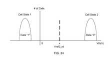
- FIG. 24shows a read operation for a cell in the SBC storage mode.
- the flash memory deviceis dynamically configurable to store data in the single bit per cell (SBC) storage mode or the multiple bit per cell (MBC) storage mode, such that both SBC data and MBC data co-exist within the same memory array.
- SBCsingle bit per cell
- MBCmultiple bit per cell
- Such a memory deviceis referred to as a multi-mode flash memory device.
- One or more tag bits stored in each page of the memoryis used to indicate the type of storage mode used for storing the data in the corresponding memory block.
- a controllermonitors the number of program-erase cycles corresponding to each page for selectively changing the storage mode in order to maximize lifespan of the multi-mode flash memory device.
- the presently described embodimentsare applicable to single MBC flash memory devices such as the one shown in FIG. 1 , and a system of MBC flash memory devices such as the ones shown in FIGS. 5 and 6 .
- FIG. 5is a block diagram of a flash memory system 100 integrated with a host system 102 .
- Flash memory system 100includes a flash memory controller 104 in communication with host system 102 , and multiple multi-mode flash memory devices 106 .
- the host system 102will include a processing device such as a microcontroller, microprocessor, or a computer system.
- the flash memory system 100 of FIG. 5is configured to include one channel 108 , where multi-mode flash memory devices 106 are coupled in parallel to channel 108 .
- the memory system 100can have more or less memory devices coupled to it.
- Channel 108includes a set of common buses (not shown), which include data and control lines that are coupled to all the memory devices 106 . While not shown, each memory device is enabled/disabled with a respective chip select signal provided by flash memory controller 104 .
- the flash memory controller 104is responsible for issuing commands and data, via the channel 108 , to a selected memory device 106 based on the operation of the host system 102 . Data read from the memory devices is transferred via the channel 108 back to the flash memory controller 104 and host system 102 .
- Flash memory system 100is generally referred to as a multi-drop configuration, in which the multi-mode flash memory devices 106 are coupled in parallel with respect to channel 108 .
- the flash memory controller 104can have multiple channels, each with flash memory devices 106 coupled in the multi-drop configuration.
- Each multi-mode flash memory device 106is implemented as NAND flash memory devices having the bank memory organization previously shown in FIG. 2 .
- the flash memory devices 106can have the same capacity or different capacities.
- FIG. 6is a block diagram of a flash memory system having serially coupled memory devices.
- Flash memory system 120includes a flash memory controller 122 in communication with host system 124 , and four serially coupled multi-mode flash memory devices 126 .
- Each of the four flash memory deviceshas an input/output circuit for facilitating operation between memory devices.
- An example of a such a flash memory deviceis described in commonly owned U.S. patent application Ser. No. 11/354,023, filed on Dec. 30, 2005, and commonly owned U.S. patent application Ser. No. 11/496,278, filed on Jul. 31, 2006, the contents of which are incorporated herein by reference.
- the multi-mode flash memory deviceis set by default to store data in the MBC storage mode.
- the life span of each multi-mode flash memory deviceis extended by executing a life span extension scheme.
- FIG. 7is a flow chart illustrating a life span extension scheme.
- the first stepis the cell conversion 200 , typically executed in response to a programming instruction.
- the program/erase cycles for all the subdivisions configured in the MBC storage modeare monitored, and any subdivision reaching a predetermined limit will automatically be converted to the SBC storage mode.
- a subdivisionis the smallest unit or grouping of cells that are convertible, such as a memory block or a page, for example. This is due to the fact that any MBC storage mode subdivision reaching the predetermined limit will no longer store data reliably, but they can be used for storing data in the SBC storage mode for a set number of program/erase cycles.
- the cell conversion algorithmwill also convert subdivisions from the SBC storage mode to the MBC storage mode, if the data stored therein is no longer retained.
- datais programmed according to the selected storage mode.
- all the subdivisions of the memory bankare set to store data in the MBC storage mode.
- at least the required number of subdivisionsare allocated and set for storing the data file in the SBC storage mode.
- the flash memory controller( 104 or 122 for example) can be configured to recognize specific data file extension types as being those that require higher storage reliability. For example, executable applications with an “.exe” in the WindowsTM operating system platform will be stored in the SBC storage mode while a video data file with an “.avi” extension does not require higher storage reliability. Therefore, the subdivisions configured in the SBC storage mode will have a longer life span than subdivisions configured in the MBC storage mode.
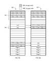
- FIGS. 8 a and 8 bgraphically illustrate the conversion of subdivisions of the memory from the MBC storage mode to the SBC storage mode, and vice versa, where a subdivision is presently a memory block.
- the multi-mode flash memory device 300 of FIG. 8 aconsists of four memory blocks 302 , each of the four memory blocks including four pages 304 . It is presumed that the memory device 300 had all its blocks 302 initially set to store data in the MBC storage mode, and has been subjected to either the user or the automatic cell conversion algorithms previously described in FIG. 7 .
- the multi-mode flash memory device 300has the configuration of SBC and MBC pages as shown in FIG. 8 a , where the shaded blocks are set to store data in the SBC storage mode and the non-shaded blocks are set to store data in the MBC storage mode.
- FIG. 8 billustrates the mapping of the multi-mode flash memory device 300 after pages 304 have been converted.
- the MBC storage mode block containing pages 306 , 308 , 310 and 312has reached a predetermined number of program/erase cycles. Therefore, they are converted to the SBC storage mode.
- the program/erase cyclesare monitored for each page 304 in the block 302 , and block conversion is executed when at least one of the pages reaches the predetermined number.
- the SBC storage mode block containing pages 314 , 315 , 316 and 317are no longer storing data. This can be determined when the data therein is erased and no other data is stored therein.
- the number of SBC program/erase cycles for SBC pages 314 , 315 , 316 and 317is checked, and because at least one of their respective SBC program/erase cycles has reached a predetermined limit, the entire block is converted back to the MBC storage mode. Specific details regarding the MBC to SBC storage mode and SBC to MBC storage mode conversion will be discussed later.
- FIGS. 8 a and 8 billustrate the conversion of block based subdivisions between the SBC storage mode and the MBC storage mode.
- FIGS. 8 c and 8 dillustrate the conversion of page based subdivisions between the SBC storage mode and the MBC storage mode.
- pages 318 and 320are set to store data in the MBC storage mode
- pages 322 and 324are set to store data in the SBC storage mode.
- individual page conversion to the SBC storage modeis executed.
- individual page conversion to the MBC storage modeis executed.
- FIG. 9is a diagrammatic illustration of a page 304 , specifically showing its allocated fields.
- Page 304includes a user data field 350 and a spare data field 352 .
- User data field 350stores data received from the user, while spare data field 352 is reserved for use by the flash device or flash memory controller.
- spare data field 352is reserved for use by the flash device or flash memory controller.
- user data field 350is 2 KB in size while the spare data field 352 is 64 B in size.
- one or more bitsare designated as a storage mode tag 354 , and several bits are designated as a program/erase cycle counter 356 for tracking the number of MBC program/erase cycles executed upon the page.
- An SBC counter 358is included to track the total number of SBC program/erase cycles executed upon the page to support SBC to MBC and subsequent MBC to SBC conversions.
- One example applicationis to program data at high speed using the SBC storage mode, and then convert to MBC storage mode later to improve memory capacity during an idle period.
- An optional lock bit 360can be provided for preventing an SBC storage mode page from being converted to the MBC storage mode. Further details of this feature will be discussed later.
- memory block 302will include any number of pages 304 , any one or more of the pages 304 can be selected for storing the tag bit, the SBC counter value, the MBC counter value and the optional lock bit corresponding to the memory block 302 .
- the mode tag 354is used by the multi-mode flash memory device 300 to determine the specific read, program and erase algorithm to use.
- read and program algorithmsthat involve setting of specific voltage levels and timing of control signals differ for data stored in the SBC and MBC storage modes. Such differences are well known to those skilled in the art.
- the flash devicewill execute MBC storage mode algorithms. Otherwise, the flash device will execute SBC storage mode algorithms. Execution of the algorithms specific to the SBC and MBC storage modes is governed by the command decoder and logic circuits of the multi-mode flash memory device.
- the multi-mode flash memory devicewill include all the circuits and control logic required for executing operations specific to both the SBC and MBC storage modes. It is noted that an MBC flash memory device typically includes all the circuits used by an SBC flash memory device. The main difference between dedicated MBC and SBC flash memory devices is the control circuitry and logic circuits for executing the algorithms.
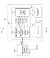
- FIG. 10is a block diagram of a flash memory system including one multi-mode flash memory device.
- Flash memory system 400includes a flash memory controller 402 and a multi-mode flash memory device 404 . While only one device 404 is shown for convenience of illustration, the system 400 can include any number of devices 404 coupled to the same channel, and the system 400 can include any number of channels. Details of the flash memory controller 402 and multi-mode flash memory device 404 will now be described.
- a typical component of the flash memory controller 402is a logical to physical address translator 406 , which is responsible for mapping each logical address provided by the host system to a corresponding physical address in the multi-mode flash memory device.
- address mappingis used to ensure that the logical address for data consistently points to its actual physical location in the memory array if the data is moved or reprogrammed to implement wear leveling operations.
- the translatoris commonly implemented as an address mapping table.
- each mode tag (MODE) of each subdivision of the multi-mode flash memory device 404is obtained and stored with its corresponding logical address entry in the mapping table. If the subdivision is a block, then the corresponding mode tag for the logical addresses corresponding to the block is stored. Alternately, if the subdivision is a page, then the mode tag of each page is obtained and stored. Therefore, the flash memory controller 402 will issue external commands (CMD) with information relating to the type of storage mode associated with the selected addresses.
- CMDexternal commands
- the multi-mode flash memory device 404 shown in FIG. 10includes a multi-mode control circuit 405 consisting of command decoder 408 and control logic 410 , flash memory circuitry 412 and a memory array 414 .
- Flash memory circuitry 412 and memory array 414have been simplified for sake of clarity, however those skilled in the art should understand that these circuit blocks include all the necessary components to ensure proper operation of the multi-mode flash memory device 404 .
- the command decoder 408receives an external command CMD issued by the flash memory controller 402 , decodes the command, and issues a corresponding internal control command to the control logic 410 .
- Control logic 410is a state machine having logic for executing all standard SBC and MBC read and program operations, including any supplementary operations such as program verify operations.
- the control logic 410also includes logic circuitry for executing logical functions unique to the multi-mode flash memory device, as will be described later.
- the command decoder 408includes an MBC command decoder 416 , an SBC command decoder 418 and a common command decoder 420 .
- the MBC command decoder 416issues MBC storage mode specific commands, such as an MBC read command RD_MBC and an MBC program command PGM_MBC.
- the SBC command decoder 418issues SBC storage mode specific commands, such as an SBC read command RD_SBC and an SBC program command PGM_SBC.
- the common decoder 420issues commands that are not specific to memory subdivisions configured for the SBC or MBC storage modes, such as an erase command.
- the three sub-command decoders 416 , 418 and 420are shown as distinct circuit blocks to illustrate the categorization of the types of commands issued by the command decoder 408 , and does not necessarily indicate a specific circuit or grouping of logic used for generating the commands.
- flash memory system 400Prior to carrying out of the steps of the illustrated operating method, it is assumed that the mode tag information has already been loaded into the address translator 406 .
- a host requestis received, which can include a read or write request for example.
- the requestwill include the logical address for writing data to or the logical address for reading data from, the multi-mode flash memory device 404 .
- the flash memory controller 402looks up the address mapping table and generates the appropriate command CMD with an indication regarding the necessary type of storage mode operation that is required (SBC vs MBC storage mode), based on the requested logical address and the state of the corresponding mode tag in the address mapping table.
- the CMD command received by the command decoder 408is decoded, and either SBC storage mode or MBC storage mode read/program commands are issued at step 454 by MBC command decoder 416 or SBC command decoder 418 .
- the CMD commandcan be a non storage mode specific command such as an erase operation that is issued by common command decoder 420 .
- the control logic 410executes the required algorithm and controls the necessary multi-mode flash memory circuitry 412 in the proper manner.
- the address mapping table of the flash memory controller 402is initialized with the mode tag. This is preferably done during a time when there are no user operations being executed, such as during power up of the flash memory system 400 .
- FIG. 12is a flow chart illustrating a method for initializing the address mapping table.
- the flash memory system 400is powered up.
- flash memory device 404scans its memory array to assess the logic states of all its tag bits. This is done by executing a read operation of all the pages in the flash memory device 404 , and providing only the mode tag information (MODE) to the flash memory controller 402 . If an entire page of data is read out at the same time, only the tag bit is used and the remaining data read out from the pages is ignored.
- the address mapping tableis then populated with the MODE tag data at step 504 .
- the SBC read algorithmdetects the presence or absence of an erased state of the tag bit.
- the two binary logic statescan be used to determine the SBC or MBC storage mode configuration of the subdivision (i.e. block or page for example).
- the flash memory devicewill be pre-programmed during manufacturing/testing to have all its mode tag bits set to one logic state (the erased state) indicating that data is to be programmed in the MBC storage mode.
- the flash memory device 402will be subjected to program and erase operations, whereby eventually at least one subdivision, be it a page or block of memory, will have its mode tag changed.
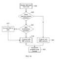
- FIG. 13is a flow chart illustrating a method for extending the life span of multi-mode flash memory device 400 by automatically changing the state of the mode tag.
- the methodoutlines specific criteria, or conditions, before a mode tag is changed.
- the methodstarts at step 550 where data is programmed to the multi-mode flash memory device. It is presumed that there is a mix of SBC storage mode subdivisions and MBC storage mode subdivisions in the memory array of the multi-mode flash memory device. Hence at step 550 , an SBC or MBC programming operation will be executed.
- the number of program cycles for each subdivision of the memory arrayis monitored after a program/erase cycle. Alternately, the monitoring can be done just prior to a program/erase cycle. It is noted that every program operation to a subdivision of the memory is preceded by an erase operation at some point, hence the number of erase cycles or program cycles is substantially the same.
- the address mapping tablecan include a program/erase counter for each subdivision, which is initially populated with a corresponding counter value stored in the spare data field ( 352 ) of the page. The counter values can be loaded during power up of the system and programmed back to the page as data is programmed. Monitoring in step 552 includes comparing the program/erase counter for the currently programmed subdivision(s) with a predetermined limit.
- MBC storage mode limitThere are two predetermined limits that are used based on the.
- One limitis the SBC storage mode limit, while the other is the MBC storage mode limit.
- MBC storage mode subdivisionswill have a limit of 10,000 program/erase cycles, and the SBC storage mode subdivision will have a limit of 100,000 program/erase cycles.
- the comparisonis executed. Then, one of three possible actions is taken if the applicable predetermined limit is reached.
- the first possible actionis to extend the life span of MBC storage mode subdivisions in step 554 by converting them to the SBC storage mode. Therefore, any data presently stored in the MBC storage mode subdivisions to be converted is either moved or programmed to available MBC storage mode subdivisions. Then the corresponding mode tag bits in the address mapping table are changed in step 556 to indicate that the subdivisions are set to the SBC storage mode.
- the tag bit field of the pageis programmed as data is programmed to the page.
- the second possible actionis to reclaim SBC storage mode subdivisions in step 558 by converting them to the MBC storage mode. This is a reverse process to the one discussed in step 554 .
- Reclamationis done under two conditions, one being that the number of SBC program/erase cycles is under a predetermined value less than the standard SBC limit, where the standard SBC limit can be 100,000 cycles. This is due to the fact that SBC memory cells programmed close to 100,000 cycles will be degraded to the point that they will not reliably store data in the MBC storage mode. Therefore, a reduced SBC to MBC reclamation limit is used. This reduced limit is selected such that the subdivision will reliably endure the standard MBC limit of 10,000 program/erase cycles.
- the reduced SBC to MBC reclamation limitwill correspond to the MBC limit.
- the MBC limitis 10,000 cycles
- the SBC memory cellscan be converted to the MBC storage mode provided they have endured 10,000 SBC program/erase cycles or less.
- the second conditionis that the data stored in the SBC subdivisions is no longer used, i.e. the data has been erased and not reprogrammed to the same subdivisions.
- the address mapping tableis updated to indicate that the subdivision is free. Once these two conditions are met, the mode tag state in the address mapping table is changed in step 556 . Therefore, it is advantageous to reclaim such SBC subdivisions for high density storage.
- the third possible actionis to retire SBC subdivisions at step 560 when they have reached their SBC program/erase cycle limit.
- the subdivisionsare simply mapped out and no longer used by the flash memory system. Mapping out of unusable subdivisions is a well-known operation in flash memory systems. However, by this point in time, the subdivision(s) will have stored data in both the MBC and SBC storage modes, thereby maximizing the lifespan of the subdivision(s).
- FIG. 14is a flow chart illustrating the method for host system selectable programming of MBC and SBC storage mode data. This method can be executed as a sub-routine of step 550 in the life span extension method of FIG. 13 .
- the flash memory controllerwill receive a programming instruction from the host and identifies the type of data to be programmed.
- the type of datacan be image files such as JPEG's, various application data files such as spreadsheet or text documents, and executable programs, for example.
- the flash memory controllerwill identify the specific data type.
- the flash memory controllerdetermines if the data file requires high reliability in step 602 . This can be done for example, by checking a table that includes all the data types considered to require high reliability. For example, executable programs can be considered to require high reliability. It is noted that the host system can pre-select the data types requiring high reliability.
- the methodproceeds to step 604 , and the multi-mode flash memory device programs the data in the MBC storage mode. More specifically, the flash memory controller identifies free subdivisions having a mode tag set to the MBC storage mode from its address mapping table, and issues the appropriate MBC programming command to the multi-mode flash memory device. Upon receiving the command, the multi-mode flash memory device will proceed with internal programming operations in the manner previously described for FIG. 10 . Once internal program verification has determined that the data has been successfully programmed, the program/erase counters in the address mapping table corresponding to the selected pages are incremented at step 606 .
- step 608the flash memory controller checks if there are free SBC storage mode subdivisions available. If free SBC storage mode subdivisions are available, then the multi-mode flash memory device is instructed to program the data into the corresponding physical locations in the SBC storage mode at step 610 . Otherwise, the necessary MBC storage mode subdivisions are converted to the SBC storage mode in step 612 by inverting the state of their mode tag. Then step 610 is executed to program the data in the SBC storage mode. Following SBC storage mode programming at step 610 , the corresponding program/erase counters are incremented at step 606 . Therefore, the user selectively programs data in either the MBC or SBC storage modes in the multi-mode flash memory device.
- the previously discussed methodcategorized data file types as being either the high or low reliability type.
- the data file typescan be categorized into different reliability levels. Then the host system can set a threshold for determining which reliability levels are to be categorized as high reliability data.
- FIG. 15is a flow chart illustrating one method for automatically converting an MBC storage mode subdivision into an SBC storage mode subdivision.
- a programming instructionis first received by the flash memory controller at step 650 .
- the programming instructionis to modify an existing file stored in the same subdivisions of the multi-mode flash memory device.
- the program/erase counter for the selected subdivision(s)is compared to the predetermined cycle limit for the MBC storage mode at step 652 . If the counter value is less than the limit, then the data is simply programmed to the same subdivisions in the multi-mode flash memory device at step 654 . Otherwise, the limit has been reached and the data is programmed to new subdivisions at step 656 .
- the original subdivisionsare erased at step 658 to clear the data.
- the states of the mode tag for the original subdivisions in the address mapping tableare inverted at step 658 , thereby designating them as SBC storage mode subdivisions.
- the subdivisions converted to the SBC storage modewill have their program/erase counters reset at step 662 , since now there are a predetermined number of SBC program/erase cycles that can be executed before the subdivisions expire and can no longer be used.
- An alternate modified sequenceis to program the data, increment the counter and then compare the program/erase counter to the predetermined cycle limit. No further action is taken if the counter value is less than the cycle limit. Otherwise, the recently programmed data is moved, or reprogrammed, to available MBC storage mode subdivisions. The reprogramming can be done whenever the system is idle. Then the original subdivisions are erased and the mode tag bits are inverted.
- the steps for programming data to SBC storage mode subdivisionsis substantially the same as the one shown in FIG. 15 .
- the MBC program/erase limitis replaced with the SBC program/erase limit, and SBC storage mode subdivisions are simply retired from use if the SBC subdivision program/erase counter is equal to the SBC program/erase limit.
- the SBC datais then programmed to an available SBC storage mode subdivision. If only MBC storage mode subdivisions are available, then the method of FIG. 14 is executed to convert the required MBC storage mode subdivisions to the SBC storage mode, and program the data.
- one countercan be used for tracking MBC program/erase cycles, and then re-used for tracking SBC program/erase cycles when converted to the SBC storage mode.
- the SBC subdivisionscan be reclaimed, then separate SBC and MBC program/erase counters are provided.
- the method of FIG. 16outlines the steps for reclaiming an SBC storage mode subdivision. This method can be executed at any time while the flash memory system is active.
- the methodstarts at step 700 by identifying each SBC storage mode subdivision that is empty, i.e. not intended to store any data.
- the SBC program/erase counteris compared to the MBC reclaim limit. If the counter is at least the reclaim limit, then the process ends at step 704 and the SBC storage mode subdivision will not be converted to the MBC storage mode. On the other hand, if the SBC program/erase counter is less than the reclaim limit, then the status of a lock bit is checked at step 706 .
- the mode tagis used for determining whether data is to be programmed with the MBC or SBC storage modes, and for executing automatic conversion between the modes. Once programmed, the mode tag is used for determining the type of read operation to be executed.
- FIG. 17is a flow chart outlining a method for reading data from the multi-mode flash memory device.
- a read instructionis received by the flash memory controller.
- the read instructionwill include a logical address of the desired data.
- the flash memory controllerwill then check its address mapping table for the state of the mode tag bits corresponding to the logical address in step 752 . If the state of the mode tag is a first state, such as a logic “1” for example, then a MBC storage mode read command CMD is generated and provided to the multi-mode flash memory device. In response, the multi-mode flash memory device will decode the command and issue an RD_MBC command at step 754 .
- the MBC readis then executed at step 756 .
- the multi-mode flash memory devicewill issue an RD_SBC command at step 758 and an SBC read is then executed at step 760 .
- the datawill be read out from the memory array and provided back to the flash memory controller. Therefore, both data programmed in the SBC and MBC storage modes can be accessed by the user from the same multi-mode flash memory device.
- FIG. 18shows a Vth (threshold voltage) distribution for an SBC storage mode cell with annotations illustrating the these parameters.
- the cell Vth window and the cell Vth distance in the MBC storage modeare much tighter than those for the SBC storage mode, since three cell states are positioned in the positive threshold voltage side. If the cell Vth window is wider, the cell Vth distance is narrower. This reduces read sensing margin and eventually it leads to failure to sense neighboring cell states. In other words, Vth overlap or even a minimum Vth gap between neighboring cell states means device failure. With an increase in the number of re-write (erase & program) cycles, the cell Vth window becomes wider by tunnel oxide degradation due to the trapped charge. The read pass voltage Vread should be lower to minimize read disturbance to unselected cells in the selected NAND cell string. However the Vread distance between Vread and the worst programmed cell Vth increases the level of Vread to position three cell states at the positive Vth side.
- FIG. 19is a graph showing how Vth shifts from ⁇ 3 V to 3 V when different step voltages (Vpgm) are used in the ISPP scheme. It can be seen that the Vth shift (Vth) due to each program pulse is directly proportional to Vpgm. Thus, a smaller Vpgm can result in a tighter Vth distribution. However, the smaller Vpgm also results in slower page program speed.
- memory cellscan store data in the SBC storage mode, either through conversion from the MBC storage mode or as a result of the need to store data with a high level of reliability.
- the memory cellscan be programmed with specific threshold voltage ranges to, for example, maximize reliability or to, for example, optimize reliability and programming speed.
- FIG. 3illustrates an example threshold voltage range distribution for an erased cell and a programmed cell in accordance with an MBC storage mode memory cell converted to an SBC storage mode memory cell.
- threshold voltage distribution schemesare provided for the SBC storage mode wherein a number of threshold voltage ranges are unused so as to provide additional space between used threshold voltage ranges.
- FIGS. 20A and 20Billustrate one example embodiment where the cell threshold voltage distribution of two levels in the SBC storage mode can be taken from threshold voltage distribution of two levels in the MBC storage mode.
- FIG. 20Ashows a threshold voltage distribution of an example MBC memory cell, similar to the example shown in FIG. 4 .
- FIG. 20Bshows a threshold voltage distribution of a memory cell configured in the SBC storage mode for where two different cell states are shown corresponding to used threshold voltage ranges.
- the cell threshold voltage distribution in the SBC storage modecan be taken from cell states 1 and 4 from the MBC storage mode as shown by arrows 800 and 802 .
- the cell threshold voltage distance between cell states 1 and 2 in the SBC storage modeis greatest. With such maximized cell threshold voltage distance in the SBC storage mode, reliability of the cell, such as endurance and retention, is enhanced.
- FIGS. 21A and 21Billustrates another example embodiment of the target cell threshold voltage distribution of two levels in the SBC storage mode.
- FIG. 21Ashows a threshold voltage distribution of an example MBC memory cell, similar to the example shown in FIG. 20A .
- FIG. 21Bshows a threshold voltage distribution of a memory cell configured in the SBC storage mode where two different cell states are shown corresponding to used threshold voltage ranges.
- the cell threshold voltage distribution of two levels in the SBC storage modecan be taken from cell states 1 and 3 from the MBC storage mode as shown by arrows 810 and 812 .
- the threshold voltage distribution scheme for SBC storage modeimproves program speed due to the shorter cell threshold voltage distance between the two shown levels, over the SBC storage mode embodiment of FIG. 20B .
- the requirements for internal read and program voltagesare lower than for the embodiment of FIG. 20B .
- the memory cellsexperience less stress during read and program operations.
- FIG. 22AThe programming sequence for the MBC storage mode threshold voltages of FIG. 20A or 21 A is now described with reference to the threshold voltage distribution diagrams of FIGS. 22A , 22 B and 22 C.
- memory cellsare erased before programming by input data, and the erased cell is typically read as data “ 11 ”.
- the cell statusis read as having a data “ 1 ” in both the upper page and the lower page.
- the lower pageshould be programmed first, as shown in FIG. 22A . If the input data for programming the lower page is a “1”, the cell remains in the erased status during the program cycle. More specifically, the lower page data of “1” inhibits programming.
- the input data for programming the lower pageis a data “ 0 ”, the cell is programmed to cell state 2 during the program cycle, as shown in FIG. 22A by arrow 850 .
- the upper pagecan be programmed after the lower page has been programmed. If the input data for programming the upper page is a “1”, the cell program operation is inhibited. Thus the Vth of the cell remains at cell state 1 if the lower page is programmed as data “ 1 ”, and remains at cell state 2 if the lower page is programmed as data “ 0 ” when the upper page input data is a “1”. If the input data for programming the upper page is a “0” the cell is programmed to cell state 4 as shown in FIG. 22B by arrow 852 , if the lower page is programmed as data “ 1 ”. If the input data for programming the upper page is a “0” the cell is programmed to cell state 3 as shown in FIG. 22C by arrow 854 , if the lower page is programmed as data “ 0 ”.
- memory cellsare erased before programming by input data, and the erased cell is typically read as data “ 1 ” and the programmed cell is read as data “ 0 ”.
- the cellremains in the erased status (i.e. program inhibit) during the program cycle. Otherwise, if the input data for programming is data “ 0 ”, then the cell is programmed to have the data “ 0 ” state during the program cycle.
- the read sequence in the MBC storage modeis executed as follows.
- a two-step read operation using reference read voltages Vref 1 _rd and Vref 3 _rdis required. If the cell is on with Vref 1 _rd and Vref 3 _rd, the lower page cell is read as data “ 1 ”. If the cell is off with Vref 1 _rd and Vref 3 _rd, the lower page cell is read as data “ 1 ”. If the cell is off with Vref 1 _rd, and on with Vref 3 _rd, the lower page cell is read as data “ 0 ”. If the cell is on with Vref 1 _rd, and off with Vref 3 _rd, the lower page cell is read as data “ 0 ”.
- the read operation of the MBC storage mode cellis completed as follows. To read the upper page in the MBC storage mode, a one step read operation using reference read voltage Vref 2 _rd is required. If the cell is on with Vref 2 _rd, the upper page cell is read as data “ 1 ”. If the cell is off with Vref 2 _rd, the upper page cell is read as data “ 0 ”.
- the read operation of the SBC storage mode cell having the threshold voltage distribution of FIG. 20Bis completed as follows.
- a one step read operation using reference read voltage Vref 2 _rdis required. If the cell is on with Vref 2 _rd, the upper page cell is read as data “ 1 ”. If the cell is off with Vref 2 _rd, the lower page cell is read as data “ 0 ”.
- the selective MBC or SBC processes executed by the flash memory controller and the multi-mode flash memory deviceare done transparently to the user. There are no additional instructions, or modification of instructions required from the user, as all determination of SBC/MBC storage mode operations are done by the flash memory controller. Accordingly, there is minimal overhead required for implementing the presently described flash memory system with a host system.
- the previously described embodiments of the multi-mode flash memory devicecan be controlled to selectively program data in the SBC storage mode or the MBC storage mode, such that data programmed in both storage modes co-exist within the same memory array at the same time.
- the selective programmingcan be done under user control based on the type of data being programmed, and/or automatically through preset algorithms.
- the life span of the multi-mode flash memory deviceis extended over flash memory devices dedicated to storing data only in the MBC storage mode.
- the subdivisions referred to in the previously described embodimentscan be memory banks, memory blocks or pages.
Landscapes
- Engineering & Computer Science (AREA)
- Theoretical Computer Science (AREA)
- Physics & Mathematics (AREA)
- General Engineering & Computer Science (AREA)
- General Physics & Mathematics (AREA)
- Microelectronics & Electronic Packaging (AREA)
- Computer Hardware Design (AREA)
- Software Systems (AREA)
- Techniques For Improving Reliability Of Storages (AREA)
- Read Only Memory (AREA)
- Memory System (AREA)
Abstract
Description
- Cell Vth Window: is the maximum range of cell threshold voltage distribution for each cell state. By example, the cell threshold voltage window in multilevel flash memory is between 0.5 to 1.0V, where a tighter range is preferred.
- Cell Vth Distance: is the distance between a worst threshold voltage in neighboring cells. By example, the cell threshold voltage window in multilevel flash memory is between 0.7 to 1.0V, where a wider distance is preferred.
- Vread Distance to Worst Programmed Cell Vth: is the distance between a read pass voltage Vread and the worst threshold voltage of a cell state having the highest threshold voltage. For the distance, wider is preferred, however lower is preferred for the level of Vread.
Claims (20)
Priority Applications (2)
| Application Number | Priority Date | Filing Date | Title |
|---|---|---|---|
| US13/757,250US8553457B2 (en) | 2007-02-16 | 2013-02-01 | Non-volatile memory with dynamic multi-mode operation |
| US14/022,805US8767461B2 (en) | 2007-02-16 | 2013-09-10 | Non-volatile memory with dynamic multi-mode operation |
Applications Claiming Priority (5)
| Application Number | Priority Date | Filing Date | Title |
|---|---|---|---|
| US89025207P | 2007-02-16 | 2007-02-16 | |
| US11/829,410US7646636B2 (en) | 2007-02-16 | 2007-07-27 | Non-volatile memory with dynamic multi-mode operation |
| US12/635,280US8045377B2 (en) | 2007-02-16 | 2009-12-10 | Non-volatile memory with dynamic multi-mode operation |
| US13/239,813US8391064B2 (en) | 2007-02-16 | 2011-09-22 | Non-volatile memory with dynamic multi-mode operation |
| US13/757,250US8553457B2 (en) | 2007-02-16 | 2013-02-01 | Non-volatile memory with dynamic multi-mode operation |
Related Parent Applications (1)
| Application Number | Title | Priority Date | Filing Date |
|---|---|---|---|
| US13/239,813ContinuationUS8391064B2 (en) | 2007-02-16 | 2011-09-22 | Non-volatile memory with dynamic multi-mode operation |
Related Child Applications (1)
| Application Number | Title | Priority Date | Filing Date |
|---|---|---|---|
| US14/022,805ContinuationUS8767461B2 (en) | 2007-02-16 | 2013-09-10 | Non-volatile memory with dynamic multi-mode operation |
Publications (2)
| Publication Number | Publication Date |
|---|---|
| US20130141973A1 US20130141973A1 (en) | 2013-06-06 |
| US8553457B2true US8553457B2 (en) | 2013-10-08 |
Family
ID=39689589
Family Applications (5)
| Application Number | Title | Priority Date | Filing Date |
|---|---|---|---|
| US11/829,410Active2028-05-22US7646636B2 (en) | 2007-02-16 | 2007-07-27 | Non-volatile memory with dynamic multi-mode operation |
| US12/635,280Active2027-08-18US8045377B2 (en) | 2007-02-16 | 2009-12-10 | Non-volatile memory with dynamic multi-mode operation |
| US13/239,813ActiveUS8391064B2 (en) | 2007-02-16 | 2011-09-22 | Non-volatile memory with dynamic multi-mode operation |
| US13/757,250ActiveUS8553457B2 (en) | 2007-02-16 | 2013-02-01 | Non-volatile memory with dynamic multi-mode operation |
| US14/022,805ActiveUS8767461B2 (en) | 2007-02-16 | 2013-09-10 | Non-volatile memory with dynamic multi-mode operation |
Family Applications Before (3)
| Application Number | Title | Priority Date | Filing Date |
|---|---|---|---|
| US11/829,410Active2028-05-22US7646636B2 (en) | 2007-02-16 | 2007-07-27 | Non-volatile memory with dynamic multi-mode operation |
| US12/635,280Active2027-08-18US8045377B2 (en) | 2007-02-16 | 2009-12-10 | Non-volatile memory with dynamic multi-mode operation |
| US13/239,813ActiveUS8391064B2 (en) | 2007-02-16 | 2011-09-22 | Non-volatile memory with dynamic multi-mode operation |
Family Applications After (1)
| Application Number | Title | Priority Date | Filing Date |
|---|---|---|---|
| US14/022,805ActiveUS8767461B2 (en) | 2007-02-16 | 2013-09-10 | Non-volatile memory with dynamic multi-mode operation |
Country Status (9)
| Country | Link |
|---|---|
| US (5) | US7646636B2 (en) |
| EP (2) | EP2126923B1 (en) |
| JP (3) | JP5421127B2 (en) |
| KR (6) | KR100938334B1 (en) |
| CN (1) | CN101617372B (en) |
| CA (1) | CA2675565C (en) |
| ES (1) | ES2477493T3 (en) |
| TW (1) | TWI449049B (en) |
| WO (1) | WO2008098363A1 (en) |
Cited By (5)
| Publication number | Priority date | Publication date | Assignee | Title |
|---|---|---|---|---|
| US8767461B2 (en)* | 2007-02-16 | 2014-07-01 | Conversant Intellectual Property Management Inc. | Non-volatile memory with dynamic multi-mode operation |
| US20150052291A1 (en)* | 2013-08-19 | 2015-02-19 | Fujitsu Limited | Semiconductor storage device and semiconductor storage device control method |
| US9280462B2 (en)* | 2013-03-15 | 2016-03-08 | Samsung Electronics Co., Ltd. | Nonvolatile storage device and operating system (OS) image program method thereof |
| TWI714267B (en)* | 2019-09-18 | 2020-12-21 | 華邦電子股份有限公司 | Non-volatile memory and data writing method thereof |
| US10956067B2 (en)* | 2018-11-21 | 2021-03-23 | Tdk Corporation | Memory controller and flash memory system having the same |
Families Citing this family (126)
| Publication number | Priority date | Publication date | Assignee | Title |
|---|---|---|---|---|
| US20090193184A1 (en)* | 2003-12-02 | 2009-07-30 | Super Talent Electronics Inc. | Hybrid 2-Level Mapping Tables for Hybrid Block- and Page-Mode Flash-Memory System |
| US7852654B2 (en)* | 2006-12-28 | 2010-12-14 | Hynix Semiconductor Inc. | Semiconductor memory device, and multi-chip package and method of operating the same |
| TWI368224B (en)* | 2007-03-19 | 2012-07-11 | A Data Technology Co Ltd | Wear-leveling management and file distribution management of hybrid density memory |
| US7460398B1 (en)* | 2007-06-19 | 2008-12-02 | Micron Technology, Inc. | Programming a memory with varying bits per cell |
| KR101379820B1 (en)* | 2007-10-17 | 2014-04-01 | 삼성전자주식회사 | Apparatus for multi-bit programming and memory data detection apparatus |
| US8001316B2 (en)* | 2007-12-27 | 2011-08-16 | Sandisk Il Ltd. | Controller for one type of NAND flash memory for emulating another type of NAND flash memory |
| US7949851B2 (en)* | 2007-12-28 | 2011-05-24 | Spansion Llc | Translation management of logical block addresses and physical block addresses |
| US9477587B2 (en)* | 2008-04-11 | 2016-10-25 | Micron Technology, Inc. | Method and apparatus for a volume management system in a non-volatile memory device |
| US8464021B2 (en)* | 2008-05-28 | 2013-06-11 | Spansion Llc | Address caching stored translation |
| US20100017649A1 (en)* | 2008-07-19 | 2010-01-21 | Nanostar Corporation | Data storage system with wear-leveling algorithm |
| US20100017556A1 (en)* | 2008-07-19 | 2010-01-21 | Nanostar Corporationm U.S.A. | Non-volatile memory storage system with two-stage controller architecture |
| KR20100010355A (en) | 2008-07-22 | 2010-02-01 | 삼성전자주식회사 | Multi-bit flash memory device and program and erase methods for the same |
| KR101038167B1 (en) | 2008-09-09 | 2011-05-31 | 가부시끼가이샤 도시바 | Information processing device and memory management method comprising a memory management device for managing access from the processor to the memory |
| US8145855B2 (en) | 2008-09-12 | 2012-03-27 | Sandisk Technologies Inc. | Built in on-chip data scrambler for non-volatile memory |
| US8429330B2 (en)* | 2008-09-12 | 2013-04-23 | Sandisk Technologies Inc. | Method for scrambling data in which scrambling data and scrambled data are stored in corresponding non-volatile memory locations |
| JP5268617B2 (en)* | 2008-12-17 | 2013-08-21 | キヤノン株式会社 | Image forming apparatus, image forming apparatus control method, and computer program |
| TWI393142B (en)* | 2008-12-29 | 2013-04-11 | Macronix Int Co Ltd | Memory device and control method of memory device |
| US8380914B1 (en)* | 2008-12-31 | 2013-02-19 | Micron Technology, Inc. | Extended address mode for serial flash memory |
| US8040744B2 (en)* | 2009-01-05 | 2011-10-18 | Sandisk Technologies Inc. | Spare block management of non-volatile memories |
| US8700840B2 (en) | 2009-01-05 | 2014-04-15 | SanDisk Technologies, Inc. | Nonvolatile memory with write cache having flush/eviction methods |
| US8244960B2 (en)* | 2009-01-05 | 2012-08-14 | Sandisk Technologies Inc. | Non-volatile memory and method with write cache partition management methods |
| EP2374063B1 (en)* | 2009-01-05 | 2017-11-22 | SanDisk Technologies LLC | Non-volatile memory and method with write cache partitioning |
| US8094500B2 (en) | 2009-01-05 | 2012-01-10 | Sandisk Technologies Inc. | Non-volatile memory and method with write cache partitioning |
| US8266503B2 (en) | 2009-03-13 | 2012-09-11 | Fusion-Io | Apparatus, system, and method for using multi-level cell storage in a single-level cell mode |
| US8261158B2 (en) | 2009-03-13 | 2012-09-04 | Fusion-Io, Inc. | Apparatus, system, and method for using multi-level cell solid-state storage as single level cell solid-state storage |
| US8370702B2 (en)* | 2009-06-10 | 2013-02-05 | Micron Technology, Inc. | Error correcting codes for increased storage capacity in multilevel memory devices |
| US7916533B2 (en)* | 2009-06-24 | 2011-03-29 | Sandisk Corporation | Forecasting program disturb in memory by detecting natural threshold voltage distribution |
| JP2011186555A (en)* | 2010-03-04 | 2011-09-22 | Toshiba Corp | Memory management apparatus and method |
| CN101630266B (en)* | 2009-08-21 | 2013-12-18 | 成都市华为赛门铁克科技有限公司 | Method and device for loading firmware, and solid state disk |
| US8854882B2 (en) | 2010-01-27 | 2014-10-07 | Intelligent Intellectual Property Holdings 2 Llc | Configuring storage cells |
| US8661184B2 (en) | 2010-01-27 | 2014-02-25 | Fusion-Io, Inc. | Managing non-volatile media |
| KR101655306B1 (en) | 2010-02-24 | 2016-09-07 | 삼성전자주식회사 | Memory system and access method thereof |
| US9245653B2 (en) | 2010-03-15 | 2016-01-26 | Intelligent Intellectual Property Holdings 2 Llc | Reduced level cell mode for non-volatile memory |
| JP5612508B2 (en)* | 2010-03-25 | 2014-10-22 | パナソニック株式会社 | Nonvolatile memory controller and nonvolatile storage device |
| US9836370B2 (en) | 2010-11-18 | 2017-12-05 | Lenovo Enterprise Solutions (Singapore) Pte. Ltd. | Backup memory administration using an active memory device and a backup memory device |
| US8737138B2 (en)* | 2010-11-18 | 2014-05-27 | Micron Technology, Inc. | Memory instruction including parameter to affect operating condition of memory |
| EP2643761A1 (en)* | 2010-11-24 | 2013-10-02 | Sony Ericsson Mobile Communications AB | Dynamically configurable embedded flash memory for electronic devices |
| US8621328B2 (en) | 2011-03-04 | 2013-12-31 | International Business Machines Corporation | Wear-focusing of non-volatile memories for improved endurance |
| US8671240B2 (en) | 2011-07-18 | 2014-03-11 | Memory Technologies Llc | User selectable balance between density and reliability |
| JP5971509B2 (en)* | 2011-08-30 | 2016-08-17 | ソニー株式会社 | Information processing apparatus and method, and recording medium |
| US9117493B2 (en)* | 2011-09-01 | 2015-08-25 | Chengdu Haicun Ip Technology Llc | Discrete three-dimensional memory comprising off-die address/data translator |
| US9024425B2 (en)* | 2011-09-01 | 2015-05-05 | HangZhou HaiCun Information Technology Co., Ltd. | Three-dimensional memory comprising an integrated intermediate-circuit die |
| US9588883B2 (en)* | 2011-09-23 | 2017-03-07 | Conversant Intellectual Property Management Inc. | Flash memory system |
| KR20130060791A (en)* | 2011-11-30 | 2013-06-10 | 삼성전자주식회사 | Memory system, data storage device, memory card, and ssd including wear level control logic |
| US8995183B2 (en)* | 2012-04-23 | 2015-03-31 | Sandisk Technologies Inc. | Data retention in nonvolatile memory with multiple data storage formats |
| CN103455440A (en)* | 2012-06-04 | 2013-12-18 | 慧荣科技股份有限公司 | Flash memory device and data access method of flash memory |
| FR2993380B1 (en)* | 2012-07-10 | 2020-05-15 | Morpho | METHOD FOR PROTECTING A SMART CARD AGAINST A PHYSICAL ATTACK FOR MODIFYING THE LOGICAL BEHAVIOR OF A FUNCTIONAL PROGRAM |
| KR101975406B1 (en)* | 2012-07-11 | 2019-05-07 | 삼성전자주식회사 | Non_volatile memory device and memory system having the same and memory management, erase and programming methods thereof |
| US8750045B2 (en) | 2012-07-27 | 2014-06-10 | Sandisk Technologies Inc. | Experience count dependent program algorithm for flash memory |
| US8804452B2 (en) | 2012-07-31 | 2014-08-12 | Micron Technology, Inc. | Data interleaving module |
| TWI486965B (en)* | 2012-10-03 | 2015-06-01 | Pixart Imaging Inc | Communication method used for transmission port between access device and control device, and access device |
| KR101906966B1 (en) | 2012-11-05 | 2018-12-07 | 삼성전자주식회사 | Logic device and operating method of the same |
| KR102053953B1 (en)* | 2013-02-04 | 2019-12-11 | 삼성전자주식회사 | Memory system comprising nonvolatile memory device and program method thereof |
| KR20140105343A (en)* | 2013-02-22 | 2014-09-01 | 삼성전자주식회사 | Device and method for securing datausing a plurality of mode in the device |
| US9153331B2 (en)* | 2013-03-13 | 2015-10-06 | Sandisk Technologies Inc. | Tracking cell erase counts of non-volatile memory |
| CN104103318B (en)* | 2013-04-12 | 2019-11-05 | 三星电子株式会社 | Operate the method for storage control and the data storage device including storage control |
| US9519577B2 (en) | 2013-09-03 | 2016-12-13 | Sandisk Technologies Llc | Method and system for migrating data between flash memory devices |
| US9442670B2 (en) | 2013-09-03 | 2016-09-13 | Sandisk Technologies Llc | Method and system for rebalancing data stored in flash memory devices |
| US9513692B2 (en)* | 2013-09-18 | 2016-12-06 | Intel Corporation | Heterogenous memory access |
| US20150120988A1 (en)* | 2013-10-28 | 2015-04-30 | Skymedi Corporation | Method of Accessing Data in Multi-Layer Cell Memory and Multi-Layer Cell Storage Device Using the Same |
| US9612773B2 (en)* | 2013-11-21 | 2017-04-04 | Samsung Electronics Co., Ltd. | User device having a host flash translation layer (FTL), a method for transferring an erase count thereof, a method for transferring reprogram information thereof, and a method for transferring a page offset of an open block thereof |
| US9218886B2 (en)* | 2013-12-10 | 2015-12-22 | SanDisk Technologies, Inc. | String dependent parameter setup |
| US20150169228A1 (en)* | 2013-12-12 | 2015-06-18 | Sandisk Technologies Inc. | System and method of storing data at a non-volatile memory |
| JP6308433B2 (en)* | 2014-05-21 | 2018-04-11 | コニカミノルタ株式会社 | Image forming apparatus, control method, and control program |
| US9645749B2 (en)* | 2014-05-30 | 2017-05-09 | Sandisk Technologies Llc | Method and system for recharacterizing the storage density of a memory device or a portion thereof |
| US8891303B1 (en) | 2014-05-30 | 2014-11-18 | Sandisk Technologies Inc. | Method and system for dynamic word line based configuration of a three-dimensional memory device |
| JP6146675B2 (en)* | 2014-06-03 | 2017-06-14 | コニカミノルタ株式会社 | Image forming apparatus, flash memory control method, and control program |
| US9652153B2 (en) | 2014-09-02 | 2017-05-16 | Sandisk Technologies Llc | Process and apparatus to reduce declared capacity of a storage device by reducing a count of logical addresses |
| US9582203B2 (en) | 2014-09-02 | 2017-02-28 | Sandisk Technologies Llc | Process and apparatus to reduce declared capacity of a storage device by reducing a range of logical addresses |
| US9524105B2 (en) | 2014-09-02 | 2016-12-20 | Sandisk Technologies Llc | Process and apparatus to reduce declared capacity of a storage device by altering an encoding format |
| US9563362B2 (en) | 2014-09-02 | 2017-02-07 | Sandisk Technologies Llc | Host system and process to reduce declared capacity of a storage device by trimming |
| US9582193B2 (en) | 2014-09-02 | 2017-02-28 | Sandisk Technologies Llc | Triggering a process to reduce declared capacity of a storage device in a multi-storage-device storage system |
| US9552166B2 (en) | 2014-09-02 | 2017-01-24 | Sandisk Technologies Llc. | Process and apparatus to reduce declared capacity of a storage device by deleting data |
| US9563370B2 (en) | 2014-09-02 | 2017-02-07 | Sandisk Technologies Llc | Triggering a process to reduce declared capacity of a storage device |
| US9582220B2 (en) | 2014-09-02 | 2017-02-28 | Sandisk Technologies Llc | Notification of trigger condition to reduce declared capacity of a storage device in a multi-storage-device storage system |
| US9665311B2 (en) | 2014-09-02 | 2017-05-30 | Sandisk Technologies Llc | Process and apparatus to reduce declared capacity of a storage device by making specific logical addresses unavailable |
| US9158681B1 (en) | 2014-09-02 | 2015-10-13 | Sandisk Technologies Inc. | Process and apparatus to reduce declared capacity of a storage device by conditionally trimming |
| US9582202B2 (en) | 2014-09-02 | 2017-02-28 | Sandisk Technologies Llc | Process and apparatus to reduce declared capacity of a storage device by moving data |
| US9582212B2 (en) | 2014-09-02 | 2017-02-28 | Sandisk Technologies Llc | Notification of trigger condition to reduce declared capacity of a storage device |
| US9519427B2 (en) | 2014-09-02 | 2016-12-13 | Sandisk Technologies Llc | Triggering, at a host system, a process to reduce declared capacity of a storage device |
| US9524112B2 (en) | 2014-09-02 | 2016-12-20 | Sandisk Technologies Llc | Process and apparatus to reduce declared capacity of a storage device by trimming |
| JP6266479B2 (en)* | 2014-09-12 | 2018-01-24 | 東芝メモリ株式会社 | Memory system |
| TWI514251B (en)* | 2014-10-09 | 2015-12-21 | Realtek Semiconductor Corp | Data allocation method and device |
| KR20160052278A (en) | 2014-11-04 | 2016-05-12 | 에스케이하이닉스 주식회사 | Semiconductor device and operating method thereof |
| KR102297541B1 (en) | 2014-12-18 | 2021-09-06 | 삼성전자주식회사 | Storage device and storage system storing data based on reliability of memory area |
| KR102295208B1 (en) | 2014-12-19 | 2021-09-01 | 삼성전자주식회사 | Storage device dynamically allocating program area and program method thererof |
| KR102282962B1 (en)* | 2014-12-22 | 2021-07-30 | 삼성전자주식회사 | Storage device and method for operating storage device |
| US10788994B1 (en)* | 2014-12-30 | 2020-09-29 | EMC IP Holding Company LLC | Disaggregation of flash management |
| TWI544490B (en) | 2015-02-05 | 2016-08-01 | 慧榮科技股份有限公司 | Data storage device and data maintenance method thereof |
| KR20160108659A (en) | 2015-03-04 | 2016-09-20 | 에스케이하이닉스 주식회사 | Operating method of semiconductor memory device and memory system including semiconductor memory device |
| US9639282B2 (en) | 2015-05-20 | 2017-05-02 | Sandisk Technologies Llc | Variable bit encoding per NAND flash cell to improve device endurance and extend life of flash-based storage devices |
| US9606737B2 (en) | 2015-05-20 | 2017-03-28 | Sandisk Technologies Llc | Variable bit encoding per NAND flash cell to extend life of flash-based storage devices and preserve over-provisioning |
| US10096355B2 (en)* | 2015-09-01 | 2018-10-09 | Sandisk Technologies Llc | Dynamic management of programming states to improve endurance |
| US9401216B1 (en) | 2015-09-22 | 2016-07-26 | Sandisk Technologies Llc | Adaptive operation of 3D NAND memory |
| US9691473B2 (en) | 2015-09-22 | 2017-06-27 | Sandisk Technologies Llc | Adaptive operation of 3D memory |
| WO2017058218A1 (en) | 2015-09-30 | 2017-04-06 | Hewlett Packard Enterprise Development LP. | Using a memory controller to manage access to a memory based on a memory initialization state indicator |
| KR102424702B1 (en)* | 2015-11-19 | 2022-07-25 | 삼성전자주식회사 | Non-volatile memory module and electronic device having the same |
| US9946483B2 (en) | 2015-12-03 | 2018-04-17 | Sandisk Technologies Llc | Efficiently managing unmapped blocks to extend life of solid state drive with low over-provisioning |
| US9946473B2 (en) | 2015-12-03 | 2018-04-17 | Sandisk Technologies Llc | Efficiently managing unmapped blocks to extend life of solid state drive |
| US10007458B2 (en)* | 2015-12-18 | 2018-06-26 | Microsemi Solutions (U.S.), Inc. | Method of configuring memory cells in a solid state drive based on read/write activity and controller therefor |
| JP6156710B2 (en)* | 2016-05-16 | 2017-07-05 | ソニー株式会社 | Information processing apparatus and method, and recording medium |
| US10121555B2 (en)* | 2016-05-26 | 2018-11-06 | Advanced Micro Devices, Inc. | Wear-limiting non-volatile memory |
| US10055158B2 (en) | 2016-09-22 | 2018-08-21 | Qualcomm Incorporated | Providing flexible management of heterogeneous memory systems using spatial quality of service (QoS) tagging in processor-based systems |
| US9971537B1 (en)* | 2016-10-26 | 2018-05-15 | Pure Storage, Inc. | Hardware support to track and transition flash LUNs into SLC mode |
| JP6789788B2 (en)* | 2016-12-12 | 2020-11-25 | 株式会社メガチップス | Memory device, controller, host device, data processing system, control program, memory device operation method and host device operation method |
| US10282094B2 (en)* | 2017-03-31 | 2019-05-07 | Samsung Electronics Co., Ltd. | Method for aggregated NVME-over-fabrics ESSD |
| CN109378027A (en)* | 2017-08-09 | 2019-02-22 | 光宝科技股份有限公司 | Control method of solid state storage device |
| DE102017221710A1 (en)* | 2017-12-01 | 2019-06-06 | Continental Automotive Gmbh | Data storage device for a motor vehicle |
| US11288116B2 (en)* | 2018-02-15 | 2022-03-29 | Micron Technology, Inc. | End of service life of data storage devices |
| JP7128088B2 (en)* | 2018-11-02 | 2022-08-30 | キオクシア株式会社 | memory system |
| KR102704708B1 (en)* | 2018-11-09 | 2024-09-10 | 에스케이하이닉스 주식회사 | Memory system and operation method thereof |
| KR102745459B1 (en)* | 2018-12-18 | 2024-12-20 | 에스케이하이닉스 주식회사 | Smart car system |
| US11194473B1 (en)* | 2019-01-23 | 2021-12-07 | Pure Storage, Inc. | Programming frequently read data to low latency portions of a solid-state storage array |
| US10817187B2 (en) | 2019-01-24 | 2020-10-27 | Western Digital Technologies, Inc. | Balancing the block wearing leveling for optimum SSD endurance |
| CN111831591B (en)* | 2019-04-19 | 2022-06-07 | 澜起科技股份有限公司 | Device and method for access control of memory module |
| JP7502317B2 (en)* | 2019-04-30 | 2024-06-18 | 長江存儲科技有限責任公司 | CONTROLLER, APPARATUS AND METHOD |
| US11467761B2 (en)* | 2019-05-31 | 2022-10-11 | Micron Technology, Inc. | Memory device and method for monitoring the performances of a memory device |
| US10949126B2 (en)* | 2019-07-25 | 2021-03-16 | ScaleFlux, Inc. | Solid-state storage device speed performance and endurance through host-side data classification and embedded write caching |
| KR102840596B1 (en)* | 2019-11-28 | 2025-07-29 | 삼성전자주식회사 | Storage device, and operating method of the storage device |
| KR20220020717A (en)* | 2020-08-12 | 2022-02-21 | 삼성전자주식회사 | A memory device, a memory controller and a memory system including them |
| US11615839B2 (en) | 2021-07-06 | 2023-03-28 | Sandisk Technologies Llc | Non-volatile memory with variable bits per memory cell |
| US20230053269A1 (en)* | 2021-08-16 | 2023-02-16 | Sandisk Technologies Llc | Memory device with improved endurance |
| US20220012195A1 (en)* | 2021-09-24 | 2022-01-13 | Intel Corporation | Enabling logic for flexible configuration of memory module data width |
| US20230410923A1 (en)* | 2022-06-21 | 2023-12-21 | Sandisk Technologies Llc | Hybrid precharge select scheme to save program icc |
| US12057161B2 (en)* | 2022-06-23 | 2024-08-06 | Sandisk Technologies Llc | Memory device with unique read and/or programming parameters |
| CN118676217A (en)* | 2023-03-20 | 2024-09-20 | 力旺电子股份有限公司 | Storage transistor for charge trapping nonvolatile memory |
Citations (47)
| Publication number | Priority date | Publication date | Assignee | Title |
|---|---|---|---|---|
| US5163021A (en) | 1989-04-13 | 1992-11-10 | Sundisk Corporation | Multi-state EEprom read and write circuits and techniques |
| US5299162A (en) | 1992-02-21 | 1994-03-29 | Samsung Electronics Co., Ltd. | Nonvolatile semiconductor memory device and an optimizing programming method thereof |
| US5367484A (en) | 1993-04-01 | 1994-11-22 | Microchip Technology Incorporated | Programmable high endurance block for EEPROM device |
| US5541879A (en) | 1993-01-13 | 1996-07-30 | Samsung Electronics Co., Ltd. | Nonvolatile semiconductor memory having program verifying circuit |
| US5671388A (en) | 1995-05-03 | 1997-09-23 | Intel Corporation | Method and apparatus for performing write operations in multi-level cell storage device |
| US5671178A (en) | 1995-02-04 | 1997-09-23 | Samsung Electronics Co., Ltd. | Erase verifying circuit for a nonvolatile semiconductor memory with column redundancy |
| EP0802540A2 (en) | 1996-04-19 | 1997-10-22 | Kabushiki Kaisha Toshiba | Multilevel memory system |
| US5822256A (en) | 1994-09-06 | 1998-10-13 | Intel Corporation | Method and circuitry for usage of partially functional nonvolatile memory |
| US5835935A (en) | 1995-09-13 | 1998-11-10 | Lexar Media, Inc. | Method of and architecture for controlling system data with automatic wear leveling in a semiconductor non-volatile mass storage memory |
| US5930167A (en) | 1997-07-30 | 1999-07-27 | Sandisk Corporation | Multi-state non-volatile flash memory capable of being its own two state write cache |
| JP2000173281A (en) | 1998-12-04 | 2000-06-23 | Sony Corp | Semiconductor memory |
| US6097637A (en) | 1994-06-02 | 2000-08-01 | Intel Corporation | Dynamic single bit per cell to multiple bit per cell memory |
| US6107658A (en) | 1997-02-27 | 2000-08-22 | Kabushiki Kaisha Toshiba | Non-volatile semiconductor memory device |
| US6118705A (en) | 1998-03-13 | 2000-09-12 | Atmel Corporation | Page mode erase in a flash memory array |
| US6230233B1 (en) | 1991-09-13 | 2001-05-08 | Sandisk Corporation | Wear leveling techniques for flash EEPROM systems |
| KR20010037694A (en) | 1999-10-19 | 2001-05-15 | 박종섭 | Flash memory circuit and system |
| JP2001210082A (en) | 2000-01-24 | 2001-08-03 | Mitsubishi Electric Corp | Nonvolatile semiconductor storage device and data storage system |
| US6359810B1 (en) | 1998-03-13 | 2002-03-19 | Atmel Corporation | Page mode erase in a flash memory array |
| US6456528B1 (en)* | 2001-09-17 | 2002-09-24 | Sandisk Corporation | Selective operation of a multi-state non-volatile memory system in a binary mode |
| US20030007384A1 (en) | 2001-07-09 | 2003-01-09 | Mitsubishi Denki Kabushiki Kaisha | Nonvolatile semiconductor memory device |
| US20030053333A1 (en) | 2001-09-18 | 2003-03-20 | Rudelic John C. | Variable level memory |
| US6717847B2 (en) | 2001-09-17 | 2004-04-06 | Sandisk Corporation | Selective operation of a multi-state non-volatile memory system in a binary mode |
| US20040080979A1 (en) | 2002-10-25 | 2004-04-29 | Nexflash Technologies, Inc. | Nonvolatile semiconductor memory having three-level memory cells and program and read mapping circuits therefor |
| US6732221B2 (en) | 2001-06-01 | 2004-05-04 | M-Systems Flash Disk Pioneers Ltd | Wear leveling of static areas in flash memory |
| US6807106B2 (en) | 2001-12-14 | 2004-10-19 | Sandisk Corporation | Hybrid density memory card |
| US20050007801A1 (en) | 2001-09-17 | 2005-01-13 | Ron Barzilai | Multi-purpose non-volatile memory card |
| US6885583B2 (en) | 2002-09-26 | 2005-04-26 | Kabushiki Kaisha Toshiba | Nonvolatile semiconductor memory |
| US20050180209A1 (en) | 2004-02-15 | 2005-08-18 | M-Systems Flash Disk Pioneers, Ltd. | Method of managing a multi-bit-cell flash memory |
| US20050286297A1 (en) | 2004-06-25 | 2005-12-29 | Micron Technology, Inc. | Multiple level cell memory device with single bit per cell, re-mappable memory block |
| US20060004952A1 (en) | 2004-02-15 | 2006-01-05 | M-Systems Flash Disk Pioneers, Ltd. | Method of managing a multi-bit-cell flash memory |
| US20060050594A1 (en) | 2004-09-03 | 2006-03-09 | Park Jin S | Flash memory device and method of erasing flash memory cell thereof |
| WO2006046425A1 (en) | 2004-10-29 | 2006-05-04 | Matsushita Electric Industrial Co., Ltd. | Nonvolatile storage device and nonvolatile storage system |
| US20060133155A1 (en) | 2004-12-08 | 2006-06-22 | Kabushiki Kaisha Toshiba | Nonvolatile semiconductor memory device and a method of erasing data thereof |
| US7082056B2 (en) | 2004-03-12 | 2006-07-25 | Super Talent Electronics, Inc. | Flash memory device and architecture with multi level cells |
| US7111140B2 (en) | 1995-07-31 | 2006-09-19 | Lexar Media, Inc. | Increasing the memory performance of flash memory devices by writing sectors simultaneously to multiple flash memory devices |
| US20060282610A1 (en) | 2005-06-08 | 2006-12-14 | M-Systems Flash Disk Pioneers Ltd. | Flash memory with programmable endurance |
| US20070025151A1 (en) | 2005-07-28 | 2007-02-01 | Jin-Yub Lee | Flash memory device capable of storing multi-bit data and single-bit data |
| WO2007067768A1 (en) | 2005-12-09 | 2007-06-14 | Micron Technology, Inc. | Single level cell programming in a multiple level cell non-volatile memory device |
| WO2007084079A1 (en) | 2006-01-18 | 2007-07-26 | Trek 2000 International Ltd. | Portable data storage device incorporating multiple flash memory units |
| US20070211530A1 (en) | 2006-03-09 | 2007-09-13 | Takeshi Nakano | Data recording method of semiconductor integrated circuit device |
| US7308525B2 (en)* | 2005-01-10 | 2007-12-11 | Sandisk Il Ltd. | Method of managing a multi-bit cell flash memory with improved reliablility and performance |
| US20080062760A1 (en) | 2006-09-13 | 2008-03-13 | Mosaid Technologies Incorporated | Flash multi-level threshold distribution scheme |
| US20080077728A1 (en) | 2006-09-27 | 2008-03-27 | Samsung Electronics Co., Ltd | Mapping information managing apparatus and method for non-volatile memory supporting different cell types |
| US7508732B2 (en) | 2006-10-26 | 2009-03-24 | Samsung Electronics Co., Ltd. | Multi-bit flash memory device including memory cells storing different numbers of bits |
| US7646636B2 (en) | 2007-02-16 | 2010-01-12 | Mosaid Technologies Incorporated | Non-volatile memory with dynamic multi-mode operation |
| US7804718B2 (en) | 2007-03-07 | 2010-09-28 | Mosaid Technologies Incorporated | Partial block erase architecture for flash memory |
| US7836242B2 (en) | 2006-01-26 | 2010-11-16 | Nuvoton Technology Corporation | Method for page random write and read in blocks of flash memory |
Family Cites Families (8)
| Publication number | Priority date | Publication date | Assignee | Title |
|---|---|---|---|---|
| JPH11224491A (en)* | 1997-12-03 | 1999-08-17 | Sony Corp | Non-volatile semiconductor memory and ic memory card using it |
| JPH11176178A (en)* | 1997-12-15 | 1999-07-02 | Sony Corp | Nonvolatile semiconductor memory device and IC memory card using the same |
| JP2001006374A (en)* | 1999-06-17 | 2001-01-12 | Hitachi Ltd | Semiconductor storage device and system |
| JP4270994B2 (en) | 2003-09-29 | 2009-06-03 | 株式会社東芝 | Nonvolatile semiconductor memory device |
| US7852654B2 (en)* | 2006-12-28 | 2010-12-14 | Hynix Semiconductor Inc. | Semiconductor memory device, and multi-chip package and method of operating the same |
| US8825939B2 (en) | 2007-12-12 | 2014-09-02 | Conversant Intellectual Property Management Inc. | Semiconductor memory device suitable for interconnection in a ring topology |
| US8261158B2 (en)* | 2009-03-13 | 2012-09-04 | Fusion-Io, Inc. | Apparatus, system, and method for using multi-level cell solid-state storage as single level cell solid-state storage |
| US8266503B2 (en)* | 2009-03-13 | 2012-09-11 | Fusion-Io | Apparatus, system, and method for using multi-level cell storage in a single-level cell mode |
- 2007
- 2007-07-27USUS11/829,410patent/US7646636B2/enactiveActive
- 2008
- 2008-02-14KRKR1020097011082Apatent/KR100938334B1/enactiveActive
- 2008-02-14CNCN200880005252.6Apatent/CN101617372B/enactiveActive
- 2008-02-14KRKR1020137033288Apatent/KR20140013079A/ennot_activeCeased
- 2008-02-14EPEP08714608.0Apatent/EP2126923B1/enactiveActive
- 2008-02-14CACA2675565Apatent/CA2675565C/ennot_activeExpired - Fee Related
- 2008-02-14KRKR1020137020922Apatent/KR20130098439A/ennot_activeCeased
- 2008-02-14EPEP12003879.9Apatent/EP2490224A3/ennot_activeWithdrawn
- 2008-02-14KRKR1020097012054Apatent/KR20090081426A/ennot_activeCeased
- 2008-02-14ESES08714608.0Tpatent/ES2477493T3/enactiveActive
- 2008-02-14WOPCT/CA2008/000285patent/WO2008098363A1/enactiveApplication Filing
- 2008-02-14KRKR1020167008455Apatent/KR20160043121A/ennot_activeCeased
- 2008-02-14JPJP2009549749Apatent/JP5421127B2/ennot_activeExpired - Fee Related
- 2008-02-14KRKR1020147033804Apatent/KR20140146229A/ennot_activeCeased
- 2008-02-15TWTW097105441Apatent/TWI449049B/enactive
- 2009
- 2009-12-10USUS12/635,280patent/US8045377B2/enactiveActive
- 2011
- 2011-09-22USUS13/239,813patent/US8391064B2/enactiveActive
- 2013
- 2013-02-01USUS13/757,250patent/US8553457B2/enactiveActive
- 2013-08-01JPJP2013160457Apatent/JP2013229100A/ennot_activeWithdrawn
- 2013-09-10USUS14/022,805patent/US8767461B2/enactiveActive
- 2015
- 2015-04-22JPJP2015087437Apatent/JP2015156251A/enactivePending
Patent Citations (63)
| Publication number | Priority date | Publication date | Assignee | Title |
|---|---|---|---|---|
| US5163021A (en) | 1989-04-13 | 1992-11-10 | Sundisk Corporation | Multi-state EEprom read and write circuits and techniques |
| US6230233B1 (en) | 1991-09-13 | 2001-05-08 | Sandisk Corporation | Wear leveling techniques for flash EEPROM systems |
| US6594183B1 (en) | 1991-09-13 | 2003-07-15 | Sandisk Corporation | Wear leveling techniques for flash EEPROM systems |
| US6850443B2 (en) | 1991-09-13 | 2005-02-01 | Sandisk Corporation | Wear leveling techniques for flash EEPROM systems |
| US5299162A (en) | 1992-02-21 | 1994-03-29 | Samsung Electronics Co., Ltd. | Nonvolatile semiconductor memory device and an optimizing programming method thereof |
| US5541879A (en) | 1993-01-13 | 1996-07-30 | Samsung Electronics Co., Ltd. | Nonvolatile semiconductor memory having program verifying circuit |
| US5546341A (en) | 1993-01-13 | 1996-08-13 | Samsung Electronics Co., Ltd. | Nonvolatile semiconductor memory |
| US5367484A (en) | 1993-04-01 | 1994-11-22 | Microchip Technology Incorporated | Programmable high endurance block for EEPROM device |
| US6097637A (en) | 1994-06-02 | 2000-08-01 | Intel Corporation | Dynamic single bit per cell to multiple bit per cell memory |
| US5822256A (en) | 1994-09-06 | 1998-10-13 | Intel Corporation | Method and circuitry for usage of partially functional nonvolatile memory |
| US5671178A (en) | 1995-02-04 | 1997-09-23 | Samsung Electronics Co., Ltd. | Erase verifying circuit for a nonvolatile semiconductor memory with column redundancy |
| US5671388A (en) | 1995-05-03 | 1997-09-23 | Intel Corporation | Method and apparatus for performing write operations in multi-level cell storage device |
| US7111140B2 (en) | 1995-07-31 | 2006-09-19 | Lexar Media, Inc. | Increasing the memory performance of flash memory devices by writing sectors simultaneously to multiple flash memory devices |
| US5835935A (en) | 1995-09-13 | 1998-11-10 | Lexar Media, Inc. | Method of and architecture for controlling system data with automatic wear leveling in a semiconductor non-volatile mass storage memory |
| JPH09288896A (en) | 1996-04-19 | 1997-11-04 | Toshiba Corp | Storage system |
| EP0802540A2 (en) | 1996-04-19 | 1997-10-22 | Kabushiki Kaisha Toshiba | Multilevel memory system |
| EP1343172A2 (en) | 1996-04-19 | 2003-09-10 | Kabushiki Kaisha Toshiba | Memory system |
| US6107658A (en) | 1997-02-27 | 2000-08-22 | Kabushiki Kaisha Toshiba | Non-volatile semiconductor memory device |
| US5930167A (en) | 1997-07-30 | 1999-07-27 | Sandisk Corporation | Multi-state non-volatile flash memory capable of being its own two state write cache |
| US6118705A (en) | 1998-03-13 | 2000-09-12 | Atmel Corporation | Page mode erase in a flash memory array |
| US6359810B1 (en) | 1998-03-13 | 2002-03-19 | Atmel Corporation | Page mode erase in a flash memory array |
| JP2000173281A (en) | 1998-12-04 | 2000-06-23 | Sony Corp | Semiconductor memory |
| KR20010037694A (en) | 1999-10-19 | 2001-05-15 | 박종섭 | Flash memory circuit and system |
| JP2001210082A (en) | 2000-01-24 | 2001-08-03 | Mitsubishi Electric Corp | Nonvolatile semiconductor storage device and data storage system |
| US6732221B2 (en) | 2001-06-01 | 2004-05-04 | M-Systems Flash Disk Pioneers Ltd | Wear leveling of static areas in flash memory |
| US20030007384A1 (en) | 2001-07-09 | 2003-01-09 | Mitsubishi Denki Kabushiki Kaisha | Nonvolatile semiconductor memory device |
| US6728133B2 (en) | 2001-07-09 | 2004-04-27 | Renesas Technology Corp. | Nonvolatile semiconductor memory device |
| US6456528B1 (en)* | 2001-09-17 | 2002-09-24 | Sandisk Corporation | Selective operation of a multi-state non-volatile memory system in a binary mode |
| US6717847B2 (en) | 2001-09-17 | 2004-04-06 | Sandisk Corporation | Selective operation of a multi-state non-volatile memory system in a binary mode |
| US7554842B2 (en)* | 2001-09-17 | 2009-06-30 | Sandisk Corporation | Multi-purpose non-volatile memory card |
| US20050007801A1 (en) | 2001-09-17 | 2005-01-13 | Ron Barzilai | Multi-purpose non-volatile memory card |
| US20030053333A1 (en) | 2001-09-18 | 2003-03-20 | Rudelic John C. | Variable level memory |
| US6807106B2 (en) | 2001-12-14 | 2004-10-19 | Sandisk Corporation | Hybrid density memory card |
| US6885583B2 (en) | 2002-09-26 | 2005-04-26 | Kabushiki Kaisha Toshiba | Nonvolatile semiconductor memory |
| US20040080979A1 (en) | 2002-10-25 | 2004-04-29 | Nexflash Technologies, Inc. | Nonvolatile semiconductor memory having three-level memory cells and program and read mapping circuits therefor |
| US6847550B2 (en) | 2002-10-25 | 2005-01-25 | Nexflash Technologies, Inc. | Nonvolatile semiconductor memory having three-level memory cells and program and read mapping circuits therefor |
| US20050180209A1 (en) | 2004-02-15 | 2005-08-18 | M-Systems Flash Disk Pioneers, Ltd. | Method of managing a multi-bit-cell flash memory |
| US20060004952A1 (en) | 2004-02-15 | 2006-01-05 | M-Systems Flash Disk Pioneers, Ltd. | Method of managing a multi-bit-cell flash memory |
| KR20060133599A (en) | 2004-02-15 | 2006-12-26 | 엠시스템스 리미티드 | How to Manage Multi-Bit Cell Flash Memory |
| US7082056B2 (en) | 2004-03-12 | 2006-07-25 | Super Talent Electronics, Inc. | Flash memory device and architecture with multi level cells |
| US20050286297A1 (en) | 2004-06-25 | 2005-12-29 | Micron Technology, Inc. | Multiple level cell memory device with single bit per cell, re-mappable memory block |
| US7336531B2 (en) | 2004-06-25 | 2008-02-26 | Micron Technology, Inc. | Multiple level cell memory device with single bit per cell, re-mappable memory block |
| US20060050594A1 (en) | 2004-09-03 | 2006-03-09 | Park Jin S | Flash memory device and method of erasing flash memory cell thereof |
| US7161842B2 (en) | 2004-09-03 | 2007-01-09 | Hynix Semiconductor Inc. | Flash memory device and method of erasing flash memory cell thereof |
| WO2006046425A1 (en) | 2004-10-29 | 2006-05-04 | Matsushita Electric Industrial Co., Ltd. | Nonvolatile storage device and nonvolatile storage system |
| US20060133155A1 (en) | 2004-12-08 | 2006-06-22 | Kabushiki Kaisha Toshiba | Nonvolatile semiconductor memory device and a method of erasing data thereof |
| US7308525B2 (en)* | 2005-01-10 | 2007-12-11 | Sandisk Il Ltd. | Method of managing a multi-bit cell flash memory with improved reliablility and performance |
| US20060282610A1 (en) | 2005-06-08 | 2006-12-14 | M-Systems Flash Disk Pioneers Ltd. | Flash memory with programmable endurance |
| US7433246B2 (en) | 2005-07-28 | 2008-10-07 | Samsung Electronics Co., Ltd. | Flash memory device capable of storing multi-bit data and single-big data |
| US20070025151A1 (en) | 2005-07-28 | 2007-02-01 | Jin-Yub Lee | Flash memory device capable of storing multi-bit data and single-bit data |
| WO2007067768A1 (en) | 2005-12-09 | 2007-06-14 | Micron Technology, Inc. | Single level cell programming in a multiple level cell non-volatile memory device |
| WO2007084079A1 (en) | 2006-01-18 | 2007-07-26 | Trek 2000 International Ltd. | Portable data storage device incorporating multiple flash memory units |
| US7836242B2 (en) | 2006-01-26 | 2010-11-16 | Nuvoton Technology Corporation | Method for page random write and read in blocks of flash memory |
| US20070211530A1 (en) | 2006-03-09 | 2007-09-13 | Takeshi Nakano | Data recording method of semiconductor integrated circuit device |
| JP2007242163A (en) | 2006-03-09 | 2007-09-20 | Toshiba Corp | Data recording method for semiconductor integrated circuit device |
| US20080062760A1 (en) | 2006-09-13 | 2008-03-13 | Mosaid Technologies Incorporated | Flash multi-level threshold distribution scheme |
| US7593259B2 (en) | 2006-09-13 | 2009-09-22 | Mosaid Technologies Incorporated | Flash multi-level threshold distribution scheme |
| US20080077728A1 (en) | 2006-09-27 | 2008-03-27 | Samsung Electronics Co., Ltd | Mapping information managing apparatus and method for non-volatile memory supporting different cell types |
| US7508732B2 (en) | 2006-10-26 | 2009-03-24 | Samsung Electronics Co., Ltd. | Multi-bit flash memory device including memory cells storing different numbers of bits |
| US7646636B2 (en) | 2007-02-16 | 2010-01-12 | Mosaid Technologies Incorporated | Non-volatile memory with dynamic multi-mode operation |
| US8045377B2 (en)* | 2007-02-16 | 2011-10-25 | Mosaid Technologies Incorporated | Non-volatile memory with dynamic multi-mode operation |
| US8391064B2 (en)* | 2007-02-16 | 2013-03-05 | Mosaid Technologies Incorporated | Non-volatile memory with dynamic multi-mode operation |
| US7804718B2 (en) | 2007-03-07 | 2010-09-28 | Mosaid Technologies Incorporated | Partial block erase architecture for flash memory |
Non-Patent Citations (30)
| Title |
|---|
| "Intel Strataflash Wireless Memory (L18)", Order No. 251902, Revision 010, Aug. 1, 2005, pp. 1-106. |
| "International Patent Application No. PCT/CA2008/000285, Search Report", May 28, 2008, pp. 45-46. |
| Aritome, S. et al, A Reliable Bi-Polarity Write/Erase Technology in Flash EEPROMS, Int'l. Electron Device Meeting, Technical Digest, Dec. 9, 1990, pp. 111-114. |
| Byeon, D. et al, "An 8GB Multi-Level NAND Flash Memory with 63NM STI CMOS Process Technology", IEEE International Solid-State Circuits Conference, Feb. 7, 2005, pp. 46-46. |
| Cho et al, "A 3.3 V 1 GB Multi-Level NAND Flash Memory with Non-Uniformthreshold Voltage Distribution", Feb. 5, 2001, pp. 28-29. |
| Cho, T. et al, "A Dual-Mode NAND Flash Memory: 1 GB Nultilevel and High Performance 512-MB Single-Level Modes", IEEE Journal of Solid-State Circuits, vol. 36, No. 11, Nov. 2001, pp. 1700-1706. |
| Choi, Young, "16-GBIT MLC NAND Flash Wighs in", EEETIMES.COM, http://www.eeetimes.com/showArticle.jhtmlarticleID=201200825, Jul. 30, 2007, pp. 1-3. |
| Gal, E. et al, "Algorithms and Data Structures for Flash Memories", ACM Computing Surveys (CSUR), vol. 37, No. 2; Jun. 2005, pp. 138-163. |
| Hara, T et al, A 146-MM2 8-GB Multi-Level NAND Flash Memory with 70-NM CMOS Technology, IEEE Journal of Solid State Circuits, vol. 41, No. 1, Jan. 2006, pp. 161-169. |
| Intel Advanced Boot Block Flash Memory (C3), 28F800C, 28F160C3, 28F320C(16) Datasheet Product Features Order No. 290645, Revision: 023, May 1, 2005, pp. 1-72. |
| Jung et al, "A 3.3V 128 MB Multi-Level NAND Flash Memory for Mass Storage Applications", Feb. 8, 1996, pp. 32-33, and 412. |
| Jung, T. et al, "A 117-MM2 3.3-V Only 128-MB Multilevel NAND Flash Memory for Mass Storage Applications", IEEE Journal of Solid-State Circuits, vol. 31, No. 11, Nov. 1996, pp. 1575-1583. |
| Kim, J. et al, "1 120-MM2 64-MB NAND Flash Memory Achieving 180 NS/Byte Effective Program Speed", IEEE Journal of Solid-State Circuits, vol. 32, No. 5, May 1997, pp. 670-680. |
| Kirisawa, R. et al, A NAND Structure Cell with a New Programming Technology for Highly Reliable 5V-Only Flash EEPROM, 1990 Symposium on VLSI Technology, CH 2874-6, 90/0000-0129 1990 IEEE, Honolulu, US, Jun. 4, 1990, pp. 129-130. |
| Lee, June et al, A 90-NM CMOS 1.8-V 2-GB NAND Flash Memory for Mass Storage Applications, IEEE Journal of Solid-State Circuits, vol. 38, No. 11, Nov. 2003, pp. 1934-1942. |
| Lee, S. et al, "A 3.3V 4GB Four-Level NAND Flash Memory with 90NM CMOS Technology, ISSCC 2004/Session 2Non-Volatile Memory/2.7", IEEE International Solid-State Circuits Conference, Digest of Technical Papers, vol. 1, XPO10722148, ISBN: 0-7803-8267-6, Feb. 16, 2004, 10 pages. |
| M-Systems Flash Disk Pioneers Ltd., "Diskonchip H1 4GB (512 Mbyte) and 8 GB (1 Gbyte) High Capacity Flash Disk with NAND and x2 Technology", Data Sheet, Rev. 0.5 (Preliminary), Jan. 1, 2005, pp. 1-66. |
| Samsung Electronics Co. Ltd., "1G×8 Bit/2G×8 Bit NAND Flash Memory, K9F8G08UXM", Technical Specification, Mar. 31, 2007, pp. 1-54. |
| Samsung Electronics Co. Ltd., "1G×8 Bit/2G×8 Bit/ 4G×8 Bit NAND Flash Memory, K9XXG08UXA", Jul. 18, 2006, pp. 1-50. |
| Samsung Electronics Co. Ltd., "256 M×8 Bit/ 128M×16 Bit/512M×8 Bit NAND Flash Memory", K9K4G08U1M, K9F2G08U0M, K9F2G16U0M, Revision 1.0, May 6, 2005, pp. 1-41. |
| Samsung Electronics Co. Ltd., 2G×8BIT NAND Flash Memory, K9XXG08UXM; K9GAG08U0M, Sep. 21, 2006, pp. 1-48. |
| Samsung Electronics, "ONENAND 4G (KFW4G16Q2M-DEB6), ONENAND 2G (KFH2G16Q2M-DEB6, ONENAND 1G (KFW1G16Q2M-DEB6)" Flash Memory, ONENANDTM Specification Ver. 1.2, Dec. 23, 2005, pp. 1-125. |
| Shirota, R. et al, "A 2.3 UM2 Memory Cell Structure for 16Mb NAND EEPROMS", International Electron Devices Meeting 1990, Technical Digest; Dec. 1990, pp. 103-106. |
| Spansion, "S70GL01GN00 Mirrobit Flash 1024 Megabit, 3.0 Volt-Only Page Mode Flash Memory Featuring 110 NM Mirrorbit Process Technology", Jun. 1, 2005, pp. 1-83. |
| Suh, K. et al, "A 3.3 V 32 MB NAND Flash Memory with Incrementa Step Pulse Programming Scheme", IEEE Journal of Solid-State Circuits, vol. 30, No. 11, Nov. 1995, pp. 1149-1156. |
| Takeuchi, K. et al, "A 56NM CMOS 99MM2 8GB Multi-Level NAND Flash Memory with 10MB/S Program Throughput,Solid-State Circuits", 2006 IEEE International Conference Digest of Technical Papers, Session 7, ISBN: 1-4244-0079-1, Feb. 6, 2006, 10 pages. |
| Takeuchi, K. et al, "A Multipage Cell Architecture for High-Speed Programming Multilevel NAND Flash Memories", IEEE Journal of Solid-State Circuits, vol. 33, Issue 8, Aug. 1998, pp. 1228-1238. |
| Tanaka, T. et al, "A Quick Intelligent Page-Programming Architecture and Shielded Bitline Sensing Method for 3 V-Only NAND Flash Memory", IEEE Journal of Solid-State Circuits, vol. 29, Issue 11, Nov. 1994, pp. 1366-1373. |
| Toshiba, "16 Gbit (2G×8Bit) CMOS NAND E2PROM (Multi-Level-Cell), TC58NVG4D1DTG00", Nov. 9, 2006, pp. 1-64. |
| U.S. Appl. No. 11/829,410, Notice of Allowance dated Nov. 17, 2009, Nov. 17, 2009, pp. 1-4. |
Cited By (10)
| Publication number | Priority date | Publication date | Assignee | Title |
|---|---|---|---|---|
| US8767461B2 (en)* | 2007-02-16 | 2014-07-01 | Conversant Intellectual Property Management Inc. | Non-volatile memory with dynamic multi-mode operation |
| US9280462B2 (en)* | 2013-03-15 | 2016-03-08 | Samsung Electronics Co., Ltd. | Nonvolatile storage device and operating system (OS) image program method thereof |
| US20160162212A1 (en)* | 2013-03-15 | 2016-06-09 | Samsung Electronics Co., Ltd. | Nonvolatile storage device and operating system (os) image program method thereof |
| US9529541B2 (en)* | 2013-03-15 | 2016-12-27 | Samsung Electronics Co., Ltd. | Nonvolatile storage device and operating system (OS) image program method thereof |
| CN108804041A (en)* | 2013-03-15 | 2018-11-13 | 三星电子株式会社 | Non-volatile memory device and its operating system(OS)Image processing method |
| CN108804041B (en)* | 2013-03-15 | 2020-05-26 | 三星电子株式会社 | Nonvolatile memory device and operating system (OS) image processing method thereof |
| US20150052291A1 (en)* | 2013-08-19 | 2015-02-19 | Fujitsu Limited | Semiconductor storage device and semiconductor storage device control method |
| US9448925B2 (en)* | 2013-08-19 | 2016-09-20 | Fujitsu Limited | Semiconductor storage device and semiconductor storage device control method |
| US10956067B2 (en)* | 2018-11-21 | 2021-03-23 | Tdk Corporation | Memory controller and flash memory system having the same |
| TWI714267B (en)* | 2019-09-18 | 2020-12-21 | 華邦電子股份有限公司 | Non-volatile memory and data writing method thereof |
Also Published As
| Publication number | Publication date |
|---|---|
| KR20090081426A (en) | 2009-07-28 |
| US8767461B2 (en) | 2014-07-01 |
| KR100938334B1 (en) | 2010-01-22 |
| CA2675565A1 (en) | 2008-08-21 |
| KR20090077840A (en) | 2009-07-15 |
| US20130141973A1 (en) | 2013-06-06 |
| ES2477493T3 (en) | 2014-07-17 |
| CN101617372A (en) | 2009-12-30 |
| US20140010019A1 (en) | 2014-01-09 |
| CN101617372B (en) | 2014-03-26 |
| JP2013229100A (en) | 2013-11-07 |
| EP2126923A4 (en) | 2010-03-17 |
| EP2490224A2 (en) | 2012-08-22 |
| US7646636B2 (en) | 2010-01-12 |
| KR20130098439A (en) | 2013-09-04 |
| JP5421127B2 (en) | 2014-02-19 |
| EP2126923B1 (en) | 2014-04-09 |
| KR20140013079A (en) | 2014-02-04 |
| CA2675565C (en) | 2014-12-09 |
| US8045377B2 (en) | 2011-10-25 |
| US20080198651A1 (en) | 2008-08-21 |
| US20100174854A1 (en) | 2010-07-08 |
| JP2015156251A (en) | 2015-08-27 |
| TWI449049B (en) | 2014-08-11 |
| US20120023285A1 (en) | 2012-01-26 |
| EP2126923A1 (en) | 2009-12-02 |
| KR20140146229A (en) | 2014-12-24 |
| KR20160043121A (en) | 2016-04-20 |
| US8391064B2 (en) | 2013-03-05 |
| JP2010518546A (en) | 2010-05-27 |
| WO2008098363A8 (en) | 2008-11-06 |
| WO2008098363A1 (en) | 2008-08-21 |
| TW200845016A (en) | 2008-11-16 |
| EP2490224A3 (en) | 2013-08-21 |
Similar Documents
| Publication | Publication Date | Title |
|---|---|---|
| US8553457B2 (en) | Non-volatile memory with dynamic multi-mode operation | |
| US11150808B2 (en) | Flash memory system | |
| US7716413B2 (en) | Method of making a multi-bit-cell flash memory | |
| US8902665B2 (en) | Solid state storage system for uniformly using memory area and method controlling the same | |
| US12436685B2 (en) | Memory device for performing program operation according to incremental step pulse programming method, storage device including the same, and operating method of the memory device | |
| CN118471294A (en) | Memory device for controlling pass voltage and method of operating the same |
Legal Events
| Date | Code | Title | Description |
|---|---|---|---|
| FEPP | Fee payment procedure | Free format text:PAYOR NUMBER ASSIGNED (ORIGINAL EVENT CODE: ASPN); ENTITY STATUS OF PATENT OWNER: LARGE ENTITY | |
| AS | Assignment | Owner name:MOSAID TECHNOLOGIES INCORPORATED, CANADA Free format text:ASSIGNMENT OF ASSIGNORS INTEREST;ASSIGNOR:KIM, JIN-KI;REEL/FRAME:029746/0318 Effective date:20070726 Owner name:MOSAID TECHNOLOGIES INCORPORATED, CANADA Free format text:CHANGE OF ADDRESS DOCUMENT;ASSIGNOR:MOSAID TECHNOLOGIES INCORPORATED;REEL/FRAME:029746/0409 Effective date:20090209 | |
| STCF | Information on status: patent grant | Free format text:PATENTED CASE | |
| AS | Assignment | Owner name:CONVERSANT INTELLECTUAL PROPERTY MANAGEMENT INC., Free format text:CHANGE OF NAME;ASSIGNOR:MOSAID TECHNOLOGIES INCORPORATED;REEL/FRAME:032439/0638 Effective date:20140101 | |
| AS | Assignment | Owner name:CONVERSANT INTELLECTUAL PROPERTY MANAGEMENT INC., CANADA Free format text:CHANGE OF ADDRESS;ASSIGNOR:CONVERSANT INTELLECTUAL PROPERTY MANAGEMENT INC.;REEL/FRAME:033678/0096 Effective date:20140820 Owner name:CONVERSANT INTELLECTUAL PROPERTY MANAGEMENT INC., Free format text:CHANGE OF ADDRESS;ASSIGNOR:CONVERSANT INTELLECTUAL PROPERTY MANAGEMENT INC.;REEL/FRAME:033678/0096 Effective date:20140820 | |
| AS | Assignment | Owner name:CPPIB CREDIT INVESTMENTS INC., AS LENDER, CANADA Free format text:U.S. PATENT SECURITY AGREEMENT (FOR NON-U.S. GRANTORS);ASSIGNOR:CONVERSANT INTELLECTUAL PROPERTY MANAGEMENT INC.;REEL/FRAME:033706/0367 Effective date:20140611 Owner name:ROYAL BANK OF CANADA, AS LENDER, CANADA Free format text:U.S. PATENT SECURITY AGREEMENT (FOR NON-U.S. GRANTORS);ASSIGNOR:CONVERSANT INTELLECTUAL PROPERTY MANAGEMENT INC.;REEL/FRAME:033706/0367 Effective date:20140611 | |
| FPAY | Fee payment | Year of fee payment:4 | |
| AS | Assignment | Owner name:CPPIB CREDIT INVESTMENTS, INC., CANADA Free format text:AMENDED AND RESTATED U.S. PATENT SECURITY AGREEMENT (FOR NON-U.S. GRANTORS);ASSIGNOR:CONVERSANT INTELLECTUAL PROPERTY MANAGEMENT INC.;REEL/FRAME:046900/0136 Effective date:20180731 | |
| AS | Assignment | Owner name:CONVERSANT INTELLECTUAL PROPERTY MANAGEMENT INC., CANADA Free format text:RELEASE OF U.S. PATENT AGREEMENT (FOR NON-U.S. GRANTORS);ASSIGNOR:ROYAL BANK OF CANADA, AS LENDER;REEL/FRAME:047645/0424 Effective date:20180731 Owner name:CONVERSANT INTELLECTUAL PROPERTY MANAGEMENT INC., Free format text:RELEASE OF U.S. PATENT AGREEMENT (FOR NON-U.S. GRANTORS);ASSIGNOR:ROYAL BANK OF CANADA, AS LENDER;REEL/FRAME:047645/0424 Effective date:20180731 | |
| AS | Assignment | Owner name:CONVERSANT INTELLECTUAL PROPERTY MANAGEMENT INC., CANADA Free format text:RELEASE BY SECURED PARTY;ASSIGNOR:CPPIB CREDIT INVESTMENTS INC.;REEL/FRAME:054295/0624 Effective date:20201028 | |
| MAFP | Maintenance fee payment | Free format text:PAYMENT OF MAINTENANCE FEE, 8TH YEAR, LARGE ENTITY (ORIGINAL EVENT CODE: M1552); ENTITY STATUS OF PATENT OWNER: LARGE ENTITY Year of fee payment:8 | |
| AS | Assignment | Owner name:MOSAID TECHNOLOGIES INCORPORATED, CANADA Free format text:CHANGE OF NAME;ASSIGNOR:CONVERSANT INTELLECTUAL PROPERTY MANAGEMENT INC.;REEL/FRAME:056603/0094 Effective date:20210401 | |
| MAFP | Maintenance fee payment | Free format text:PAYMENT OF MAINTENANCE FEE, 12TH YEAR, LARGE ENTITY (ORIGINAL EVENT CODE: M1553); ENTITY STATUS OF PATENT OWNER: LARGE ENTITY Year of fee payment:12 |