US8552764B2 - Clock glitch detection circuit - Google Patents
Clock glitch detection circuitDownload PDFInfo
- Publication number
- US8552764B2 US8552764B2US13/131,349US200913131349AUS8552764B2US 8552764 B2US8552764 B2US 8552764B2US 200913131349 AUS200913131349 AUS 200913131349AUS 8552764 B2US8552764 B2US 8552764B2
- Authority
- US
- United States
- Prior art keywords
- master
- count
- slave
- counter
- comparator
- Prior art date
- Legal status (The legal status is an assumption and is not a legal conclusion. Google has not performed a legal analysis and makes no representation as to the accuracy of the status listed.)
- Active
Links
Images


Classifications
- G—PHYSICS
- G06—COMPUTING OR CALCULATING; COUNTING
- G06F—ELECTRIC DIGITAL DATA PROCESSING
- G06F1/00—Details not covered by groups G06F3/00 - G06F13/00 and G06F21/00
- G06F1/04—Generating or distributing clock signals or signals derived directly therefrom
- H—ELECTRICITY
- H03—ELECTRONIC CIRCUITRY
- H03K—PULSE TECHNIQUE
- H03K5/00—Manipulating of pulses not covered by one of the other main groups of this subclass
- H03K5/125—Discriminating pulses
- H03K5/1252—Suppression or limitation of noise or interference
Definitions
- This inventionrelates to a circuit for detecting clock glitches in a clock signal.
- the inventionalso relates to a synchronous circuit comprising a clock tree.
- the inventionfurther relates to a circuit for being integrated in the synchronous circuit.
- FIG. 1Schematically shown in FIG. 1 is a plot of an idealized clock signal 100 .
- the clock signal 100is presented, by way of example, as an electrical voltage V varying as a function of time t. More generally, the clock signal is the time-dependence of a physical quantity. For example, the clock signal could be provided optically by a variation of an intensity of light.
- the signal V(t) shown hereis a regular succession of high and low values, V 0 and V 1 , respectively. The low values last a time T 0 , the high values last a time T 1 . In the example shown, T 0 and T 1 are equal, but other ratios configurations are also commonly used in the art.
- Transitions from the low value V 0 to the high value V 1are referred to as a rising edges.
- rising edgesoccur at equidistant times t 1 , t 3 , and t 5 .
- Transitions from the high value V 1 to the low value V 0are termed falling edges.
- falling edgesoccur at equidistant times t 0 , t 2 , and t 4 .
- Rising edges and falling edgesare summarily referred to as clock edges.
- Any synchronous circuitrelies on the presence of a clock signal similar to the one illustrated in the Figure. Operations to be performed by the components of the circuit are triggered by clock edges, for example, only by rising edges, or only by falling edges, or by both falling and rising edges. After an operation has been performed, the component waits for the next edge before executing the next operation. The various components can thus be synchronized. Any component thus controlled by the clock signal is said to be clocked by the clock signal.
- Clock glitchesare a prominent root cause for many functional errors of an electronic device.
- the detection of clock glitchesis of special importance, since many common cause failures are either generated by clock glitches or will also result in clock glitches.
- the present inventionprovides circuits for detecting clock glitches in a clock signal as described in the accompanying claims.
- FIG. 1shows a schematic diagram of an example of an ideal clock signal.
- FIG. 2shows a schematic diagram of an example of a clock signal having a clock glitch.
- FIG. 3shows a schematic diagram of an example of a clock signal having a different clock glitch.
- FIG. 4schematically shows an example of an embodiment of a circuit for detecting clock glitches.
- FIG. 5schematically shows an example of an embodiment of another circuit for detecting clock glitches.
- FIG. 6schematically shows an example of an embodiment of a circuit for detecting clock glitches, the circuit comprising circuits as discussed with reference to FIG. 4 and FIG. 5 , respectively.
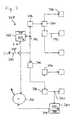
- FIG. 7schematically shows an example of an embodiment of a circuit comprising a clock tree and two detectors for detecting clock glitches.
- the circuit 402for detecting clock glitches in a clock signal 400 .
- the circuit 402comprises: a master counter 412 clocked by the clock signal 400 , for memorizing a master count N M ; an incrementer 428 for advancing the master count by one increment; and a slave counter 420 clocked by the clock signal, for memorizing a slave count N S .
- the incrementis +1.
- any other encodings and incrementsmay be used for the counter; for example hamming codes may be used for this purpose.
- the circuit 402is configured such that the slave count N S is retarded relative to the master count by at least P clock edges, the number P being greater than or equal to one.
- the circuitfurther comprises a comparator 434 for determining whether the difference N M ⁇ N S between the master count and the slave count is at least P times the increment. In the present example, P equals one.
- the slave countthus catches up with the master count. It should be noted that the slave count remains retarded relative to the master count in the sense that at any point in time the slave counter indicates the master count of a previous clock cycle. However, in the case of the master counter failing to advance, the retardation is not apparent from a difference between the master count and the slave count. After the slave counter 420 has advanced, the comparator 440 will detect that the master count and the slave count do not differ as expected, and it will generate an error signal.
- the comparator 434 or its resultmay be qualified by the clock signal 400 .
- the comparator 434may be activated or an evaluation of the comparison result may be activated by the clock signal only when a valid result signal can be delivered. Thereby it may be ensured that the slave count and the master count are compared only at a correct point in time during a clock cycle.
- the incrementer 428is combinatorial in the present example.
- the master counter 412 and the slave counter 420are wraparound counters having the same range. Their range may, for example, consist of the integer numbers from zero to 2 n ⁇ 1, where n is an integer constant. For example, the range may be zero to one (the smallest possible range), or zero to three, or zero to seven, or zero to fifteen.
- ncan be any integer number equal to or larger than one.
- the usage of different encodings or representations for the given range by the countersare also possible and often beneficial due to their better stability with respect to timing variances.
- the master counter 412comprises a storage element for memorizing the master count N M while the slave counter 420 comprises a storage element for memorizing the slave count N S .
- Each of these storage elementsmay be provided, for example, by a register, an assembly of flip-flops, a latch, or a memory.
- a register and or an assembly of flip-flopsmay be advantageous because of their greater speed, reduced size requirements or enhanced stability with respect to environmental conditions.
- the master counter 412 and the slave counter 420may be constructed in the same manner.
- the master counter 412has an input port 416 for setting the master count and an output port 418 for delivering the master count.
- the slave counter 420has an input port 424 for setting the slave count and an output port 426 for delivering the slave count.
- the master counters output port 418is coupled to the slave counters input port 424 . More specifically, the master counters output port 418 is coupled directly to the slave counters input port 424 .
- the incrementer 428has an input port 430 for receiving an input number and an output port 432 for delivering an output number, the output number being the input number plus one increment.
- the incrementmay be a constant integer number, such as +1 or ⁇ 1 or any other increment imposed by the chosen encoding for the counter values.
- the master counters output port 418is coupled to the incrementer's input port 430 and the incrementer's output port 432 is coupled to the master counters input port 416 .
- the comparator 434has a first input port 436 for receiving a first input number, a second input port 438 for receiving a second input number, and an output port 440 for delivering a comparator signal depending on the difference between the first input number and the second input number.
- the master counters output port 418is coupled to the comparators first input port 436 and the slave counters output port 426 is coupled to the comparators second input port 438 .
- Both the master counter 412 and the slave counter 420may have a capture time that is shorter than a delay of the incrementor 420 .
- the delay of the incrementoris the delay of delivering the output signal of the incrementer 434 (delivered at the output port 432 ) with respect to receiving the input signal (received at the input port 430 ).
- the capture timeis understood to be the minimum time during which an input count needs to be applied at the counters input port 416 (for the master counter 412 ) or 424 (for the slave counter 420 ) to be able to capture the input count.
- the input countis delivered at the output port 418 or 426 when the counter 412 or 420 is triggered by the subsequent clock edge (or the subsequent rising edge, or the subsequent falling edge, depending on details of the implementation). It is noted that an additional (small) delay exists between the instant at which the counter 412 or 420 receives the triggering clock edge and the instant at which the captured count is actually delivered at the output port 418 or 426 . This additional delay may be referred to as the output delay.
- the described deviceis capable to detect clock glitches faster than the intrinsic delay of the incrementer 428 , but larger than the capture time of the slave counter 420 .
- the slave countermay have a capture time not longer (e.g. shorter) than the capture times and/or reaction times of any other component of the synchronous system.
- the slave count capture timemay be chosen to be as short as possible. Thereby, it can be ensured to detect any clock glitch (faster than the intrinsic delay of the incrementer) that results in a functional effect. Otherwise it will not be detected, but also have no effect on other parts of the device.
- the circuit 402will not necessarily detect all clock glitches possibly present in the clock signal 400 .
- one or both countersmay not be modified.
- the circuit 504comprises a rising-edge counter 512 triggered by rising edges in the clock signal 500 , 700 , for memorizing a rising-edge count N R ; a falling-edge counter 542 triggered by falling edges in the clock signal, for memorizing a falling-edge count N F ; a rising-edge incrementer 528 for advancing the rising-edge count N R by one increment; a falling-edge incrementer 558 for advancing the falling-edge count N F by one increment; a comparator 574 for determining the difference N R ⁇ N F between the rising-edge count N R and the falling edge count N F , or for determining whether the rising-edge count N R and the falling edge count N F differ.
- This comparator 574 or its result 580may for example be qualified by one of both input clocks 514 or 546 to provide only valid results and not intermediate count differences. If N R and N F are found to differ, an error signal may be generated, the error signal indicating that a clock glitch has been detected.
- the circuit 504may further comprise an inverter 572 for generating an amplitude-inverted clock signal in response to the clock signal 500 or receive the inverted clock directly from another component in the system that has generated it. It may further comprise the circuit 402 as described above with reference to FIG. 4 ; in this case the rising-edge counter 512 or the falling-edge counter 542 is the master counter 412 .
- the circuit 606for detecting clock glitches in a clock signal 600 .
- the circuit 606combines features already discussed above with reference to FIGS. 4 and 5 , and is therefore discussed only briefly.
- the circuitcomprises a master counter 612 and a corresponding slave counter 620 clocked both by the clock signal 600 .
- the master-slave arrangementdetects clock glitches in the manner as described above with reference to FIG. 4 . It further comprises a master counter 642 and a corresponding slave counter 650 clocked both by an inverted clock signal generated from the clock signal 600 by inverting its amplitude.
- first master-slave arrangement 612 , 628 , 620 , 634While the first master-slave arrangement 612 , 628 , 620 , 634 is rising-edge triggered, the second master-slave arrangement 672 , 642 , 650 , 658 , 644 is falling-edge triggered.
- a first master count delivered by the first master-slave arrangement 612 , 628 , 620 , 634 at output port 618is compared to a second master count delivered by the second master-slave arrangement 672 , 642 , 650 , 658 , 644 at output port 648 by means of a comparator 674 . Should the first master count and the second master count differ, an error signal is generated.
- a comparator 674for determining the difference N R ⁇ N F between the rising-edge count N R and the falling-edge count N F may be provided.
- the rising-edge count from output 618is compared by a comparator 682 to a master count received from an output 619 of a second circuit 607 (not shown in this Figure but analogous to circuit 707 in FIG. 7 ), the second circuit 607 receiving the clock signal 600 from a different point in a clock tree (not shown in this Figure).
- the falling-edge count from output 648is compared by a comparator 684 to a corresponding falling-edge count received from an output 649 of the second circuit 607 . If the counts at outputs 648 and 649 are found to differ, an error signal is generated.
- the synchronous circuit 708 represented thereincomprises a clock tree 790 , 792 , 793 , 794 , 795 for transmitting a clock signal 700 from a start point 790 to one or more other points.
- the start point and the other pointscomprise a first point 792 and second point 793 .
- the clock tree shown herecomprises a plurality of different, similar or identical synchronous components (sinks) 794 to which the clock signal is transmitted. Some of the components 794 transmit the clock signal further to other components 794 .
- the synchronous circuit 708further comprises a first counter 712 clocked by the clock signal at the first point 792 , for memorizing a first count N 1 , a first incrementer 728 for advancing the first count N 1 by one increment, a second counter 713 clocked by the clock signal at the second point 793 , for memorizing a second count N 2 , a second incrementer 729 for advancing the second count N 2 by one increment, and a comparator 782 for determining the difference N 1 ⁇ N 2 between the first count N 1 and the second count N 1 , or for determining whether the first count N 1 and the second count N 2 differ.
- the synchronous circuit 708may comprise the circuit 402 described above with reference to FIG.
- the synchronous circuit 708may also comprise the synchronous circuit 504 discussed above with reference to FIG. 5 . That is, the synchronous circuit 708 comprises (components labeled by reference numerals beginning with a “5” are shown in FIG.
- a rising-edge counter 512triggered by rising edges in the clock signal 500 , 700 , for memorizing a rising-edge count N R ; a falling-edge counter 542 triggered by falling edges in the clock signal, for memorizing a falling-edge count N F ; a rising-edge incrementer 528 for advancing the rising-edge count N R by one increment; a falling-edge incrementer 558 for advancing the falling-edge count N F by one increment; a comparator 574 for determining the difference N R ⁇ N F between the rising-edge count N R and the falling edge count N F , or for determining whether the rising-edge count N R and the falling edge count N F differ, wherein the first counter 712 , the first count N 1 , and the first incrementer 728 are the rising-edge counter 512 , the rising-edge count N R , and the rising-edge incrementer 528 , respectively.
- the first counter 712 and the first incremeter 728are components of a distinct clock glitch detector 706 which may be connected to an arbitrary point of the clock tree.
- the clock glitch detector 706could alternatively be connected to a point 795 .
- the design of the clock glitch detector 706is analogous to the circuit 606 described above with reference to FIG. 6 .
- the second counter 713 and the second incrementer 728are components of a clock glitch detector 707 constructed in the same manner as clock glitch detector 706 .
- connectionsmay be any type of connection suitable to transfer signals from or to the respective nodes, units or devices, for example via intermediate devices. Accordingly, unless implied or stated otherwise the connections may for example be direct connections or indirect connections.
- busis used to refer to a plurality of signals or conductors which may be used to transfer one
- assertor “set” and “negate” (or “deassert” or “clear”) are used herein when referring to the rendering of a signal, status bit, or similar apparatus into its logically true or logically false state, respectively. If the logically true state is a logic level one, the logically false state is a logic level zero. And if the logically true state is a logic level zero, the logically false state is a logic level one.
- Each signal described hereinmay be designed as positive or negative logic, where negative logic can be indicated by a bar over the signal name or an asterisk (*) following the name.
- negative logicthe signal is active low where the logically true state corresponds to a logic level zero.
- positive logicthe signal is active high where the logically true state corresponds to a logic level one.
- any of the signals described hereincan be designed as either negative or positive logic signals. Therefore, in alternate embodiments, those signals described as positive logic signals may be implemented as negative logic signals, and those signals described as negative logic signals may be implemented as positive logic signals.
- the terms “rising edge” and “falling edge”are interchangeable.
- the conductors as discussed hereinmay be illustrated or described in reference to being a single conductor, a plurality of conductors, unidirectional conductors, or bidirectional conductors. However, different embodiments may vary the implementation of the conductors. For example, separate unidirectional conductors may be used rather than bidirectional conductors and vice versa. Also, plurality of conductors may be replaced with a single conductor that transfers multiple signals serially or in a time multiplexed manner. Likewise, single conductors carrying multiple signals may be separated out into various different conductors carrying subsets of these signals. Therefore, many options exist for transferring signals.
- system 708are circuitry located on a single integrated circuit or within a same device.
- system 708may include any number of separate integrated circuits or separate devices interconnected with each other.
- detector 706may be located on a same integrated circuit as detector 707 on a separate integrated circuit or located within another peripheral or slave discretely separate from other elements of system 708 .
- system 708 or portions thereofmay be soft or code representations of physical circuitry or of logical representations convertible into physical circuitry. As such, system 708 may be embodied in a hardware description language of any appropriate type.
- the inventionis not limited to physical devices or units implemented in non-programmable hardware but can also be applied in programmable devices or units able to perform the desired device functions by operating in accordance with suitable program code.
- the devicesmay be physically distributed over a number of apparatuses, while functionally operating as a single device.
- detectors 706 and 707may be connected to physically separated branches of the clock tree, the clock signal being distributed by a telecommunication modality rather than by a wire.
- devices functionally forming separate devicesmay be integrated in a single physical device.
- the two detectors 706 and 707may form a single device have ports for be coupled to different points of the clock tree.
- any reference signs placed between parenthesesshall not be construed as limiting the claim.
- the word ‘comprising’does not exclude the presence of other elements or steps then those listed in a claim.
- the terms “a” or “an,” as used herein,are defined as one or more than one.
Landscapes
- Physics & Mathematics (AREA)
- Engineering & Computer Science (AREA)
- Theoretical Computer Science (AREA)
- Nonlinear Science (AREA)
- General Engineering & Computer Science (AREA)
- General Physics & Mathematics (AREA)
- Manipulation Of Pulses (AREA)
Abstract
Description
Claims (20)
Applications Claiming Priority (1)
| Application Number | Priority Date | Filing Date | Title |
|---|---|---|---|
| PCT/IB2009/050011WO2010076667A1 (en) | 2009-01-05 | 2009-01-05 | Clock glitch detection circuit |
Related Parent Applications (1)
| Application Number | Title | Priority Date | Filing Date |
|---|---|---|---|
| PCT/IB2009/050011A-371-Of-InternationalWO2010076667A1 (en) | 2009-01-05 | 2009-01-05 | Clock glitch detection circuit |
Related Child Applications (1)
| Application Number | Title | Priority Date | Filing Date |
|---|---|---|---|
| US14/015,519DivisionUS9024663B2 (en) | 2009-01-05 | 2013-08-30 | Clock glitch detection circuit |
Publications (2)
| Publication Number | Publication Date |
|---|---|
| US20110317802A1 US20110317802A1 (en) | 2011-12-29 |
| US8552764B2true US8552764B2 (en) | 2013-10-08 |
Family
ID=41048601
Family Applications (2)
| Application Number | Title | Priority Date | Filing Date |
|---|---|---|---|
| US13/131,349ActiveUS8552764B2 (en) | 2009-01-05 | 2009-01-05 | Clock glitch detection circuit |
| US14/015,519ActiveUS9024663B2 (en) | 2009-01-05 | 2013-08-30 | Clock glitch detection circuit |
Family Applications After (1)
| Application Number | Title | Priority Date | Filing Date |
|---|---|---|---|
| US14/015,519ActiveUS9024663B2 (en) | 2009-01-05 | 2013-08-30 | Clock glitch detection circuit |
Country Status (3)
| Country | Link |
|---|---|
| US (2) | US8552764B2 (en) |
| TW (1) | TWI453427B (en) |
| WO (1) | WO2010076667A1 (en) |
Cited By (3)
| Publication number | Priority date | Publication date | Assignee | Title |
|---|---|---|---|---|
| US20150270836A1 (en)* | 2014-03-19 | 2015-09-24 | Stmicroelectronics International N.V. | Clock glitch and loss detection circuit |
| US10884448B1 (en) | 2019-09-06 | 2021-01-05 | Nuvoton Technology Corporation | Clock glitch detection circuit |
| US20220276670A1 (en)* | 2020-02-17 | 2022-09-01 | Be Spoon SAS | Clock-error estimation for two-clock electronic device |
Families Citing this family (9)
| Publication number | Priority date | Publication date | Assignee | Title |
|---|---|---|---|---|
| US8552764B2 (en) | 2009-01-05 | 2013-10-08 | Freescale Semiconductor, Inc. | Clock glitch detection circuit |
| WO2010112969A1 (en) | 2009-03-31 | 2010-10-07 | Freescale Semiconductor, Inc. | Clock glitch detection |
| US9043737B2 (en) | 2013-04-30 | 2015-05-26 | Freescale Semiconductor, Inc. | Integrated circuit design verification through forced clock glitches |
| US10163164B1 (en) | 2014-09-22 | 2018-12-25 | State Farm Mutual Automobile Insurance Company | Unmanned aerial vehicle (UAV) data collection and claim pre-generation for insured approval |
| CN110763974B (en)* | 2018-07-27 | 2022-02-18 | 创意电子股份有限公司 | Surge measuring device and method |
| TWI710770B (en)* | 2018-07-27 | 2020-11-21 | 創意電子股份有限公司 | Glitch measurement device and glitch measurement method |
| CN111211774B (en)* | 2018-11-21 | 2023-12-26 | 英业达科技有限公司 | Bounce eliminating circuit |
| US11429142B2 (en) | 2020-12-18 | 2022-08-30 | Nxp Usa, Inc. | Glitch detector |
| EP4450985A1 (en) | 2023-04-19 | 2024-10-23 | Nxp B.V. | Clock signal monitoring unit |
Citations (30)
| Publication number | Priority date | Publication date | Assignee | Title |
|---|---|---|---|---|
| GB1452559A (en) | 1973-12-20 | 1976-10-13 | Hasler Ag | Method and device for frequency multiplication |
| US4389622A (en) | 1981-09-28 | 1983-06-21 | Honeywell Inc. | System for preventing transient induced errors in phase locked loop |
| US4864158A (en)* | 1988-01-28 | 1989-09-05 | Amtech Corporation | Rapid signal validity checking apparatus |
| US5381126A (en) | 1992-07-31 | 1995-01-10 | Sgs-Thompson Microelectronics, Inc. | Programmable difference flag logic |
| US5526286A (en) | 1994-02-16 | 1996-06-11 | Tektronix, Inc. | Oversampled logic analyzer |
| US5721944A (en) | 1994-07-07 | 1998-02-24 | International Business Machines Corporation | Method and system for implementing relative time discriminations in a high speed data transmission network |
| US5764524A (en)* | 1996-02-12 | 1998-06-09 | Snap-On Technologies, Inc. | Method and apparatus for detection of missing pulses from a repetitive pulse train |
| US5812250A (en) | 1992-12-24 | 1998-09-22 | Canon Kabushiki Kaisha | Doppler velocimeter and various kinds of apparatuses for signal processing thereof |
| US5923191A (en)* | 1997-05-08 | 1999-07-13 | Vlsi Technology, Inc. | Device and a method for monitoring a system clock signal |
| KR20010059722A (en) | 1999-12-30 | 2001-07-06 | 서평원 | Method and Circuit for detecting glitch signal |
| US6285396B1 (en) | 1997-08-11 | 2001-09-04 | Nds Limited | Glitch detector |
| KR20020053267A (en) | 2000-12-27 | 2002-07-05 | 박태진 | Glitch masking method for switching signal and apparatus thereof |
| US6535024B1 (en) | 1998-09-17 | 2003-03-18 | Stmicroelectronics S.A. | Clock signal filtering circuit |
| US20030058013A1 (en) | 2001-09-26 | 2003-03-27 | Cole Steven R. | Digital interpolation window filter for phase-locked loop operation with randomly jittered reference clock |
| US6543027B1 (en) | 2000-05-18 | 2003-04-01 | 3Com Corporation | On-chip detection of clock gitches by examination of consecutive data |
| KR20030050867A (en) | 2001-12-19 | 2003-06-25 | 엘지전자 주식회사 | Glitch protection apparatus |
| US20030146778A1 (en) | 2002-02-01 | 2003-08-07 | Mcmahan Dennis B. | Method and apparatus for removing digital glitches |
| JP2006005576A (en) | 2004-06-16 | 2006-01-05 | Matsushita Electric Ind Co Ltd | Clock filter circuit and clock filter test circuit |
| US20060076984A1 (en) | 2004-10-13 | 2006-04-13 | Robin Lu | Balanced debounce circuit with noise filter for digital system |
| US20060097756A1 (en)* | 2004-11-05 | 2006-05-11 | Infineon Technologies North America Corp. | Duty distortion detector |
| US7129757B2 (en)* | 2004-11-30 | 2006-10-31 | International Business Machines Corporation | Clock frequency detect with programmable jitter tolerance |
| US20070075746A1 (en) | 2005-10-04 | 2007-04-05 | Fruhauf Serge F | System and method for glitch detection in a secure microcontroller |
| US20070120584A1 (en) | 2005-11-30 | 2007-05-31 | International Business Machines Corporation | Phase- or frequency-locked loop circuit having a glitch detector for detecting triggering-edge-type glitches in a noisy signal |
| US20070236257A1 (en) | 2006-04-11 | 2007-10-11 | Abhay Kejriwal | Debounce circuit and method |
| US7352214B2 (en) | 2004-10-06 | 2008-04-01 | Broadcom Corporation | System and method for clock detection with glitch rejection |
| JP2008103863A (en) | 2006-10-18 | 2008-05-01 | Nec Corp | Clock asynchronous switching device, circuit and method for canceling noise, and program |
| US7592843B1 (en) | 2006-07-28 | 2009-09-22 | Zilog, Inc. | Clock input filter circuit |
| US7714619B2 (en)* | 2007-10-31 | 2010-05-11 | Oki Semiconductor Co., Ltd. | High-frequency clock detection circuit |
| WO2010112969A1 (en) | 2009-03-31 | 2010-10-07 | Freescale Semiconductor, Inc. | Clock glitch detection |
| US8115516B2 (en) | 2007-06-14 | 2012-02-14 | Freescale Semiconductor, Inc. | Circuit arrangement for filtering unwanted signals from a clock signal, processing system and method of filtering unwanted signals from a clock signal |
Family Cites Families (6)
| Publication number | Priority date | Publication date | Assignee | Title |
|---|---|---|---|---|
| US4330751A (en)* | 1979-12-03 | 1982-05-18 | Norlin Industries, Inc. | Programmable frequency and duty cycle tone signal generator |
| WO2003013000A2 (en)* | 2001-08-03 | 2003-02-13 | Altera Corporation | Clock loss detection and switchover circuit |
| JP4190217B2 (en)* | 2002-06-21 | 2008-12-03 | 富士通マイクロエレクトロニクス株式会社 | Clock generation apparatus and audio data processing apparatus |
| US6747491B1 (en)* | 2003-04-10 | 2004-06-08 | Winbond Electronics Corp. | Spike free circuit for reducing EMI effect |
| US7411429B2 (en) | 2005-10-28 | 2008-08-12 | Silicon Integrated Systems Corp. | System and method for clock switching |
| US8552764B2 (en) | 2009-01-05 | 2013-10-08 | Freescale Semiconductor, Inc. | Clock glitch detection circuit |
- 2009
- 2009-01-05USUS13/131,349patent/US8552764B2/enactiveActive
- 2009-01-05WOPCT/IB2009/050011patent/WO2010076667A1/enactiveApplication Filing
- 2010
- 2010-01-04TWTW99100013Apatent/TWI453427B/ennot_activeIP Right Cessation
- 2013
- 2013-08-30USUS14/015,519patent/US9024663B2/enactiveActive
Patent Citations (32)
| Publication number | Priority date | Publication date | Assignee | Title |
|---|---|---|---|---|
| GB1452559A (en) | 1973-12-20 | 1976-10-13 | Hasler Ag | Method and device for frequency multiplication |
| US4389622A (en) | 1981-09-28 | 1983-06-21 | Honeywell Inc. | System for preventing transient induced errors in phase locked loop |
| US4864158A (en)* | 1988-01-28 | 1989-09-05 | Amtech Corporation | Rapid signal validity checking apparatus |
| US5381126A (en) | 1992-07-31 | 1995-01-10 | Sgs-Thompson Microelectronics, Inc. | Programmable difference flag logic |
| US5812250A (en) | 1992-12-24 | 1998-09-22 | Canon Kabushiki Kaisha | Doppler velocimeter and various kinds of apparatuses for signal processing thereof |
| US5526286A (en) | 1994-02-16 | 1996-06-11 | Tektronix, Inc. | Oversampled logic analyzer |
| US5721944A (en) | 1994-07-07 | 1998-02-24 | International Business Machines Corporation | Method and system for implementing relative time discriminations in a high speed data transmission network |
| US5764524A (en)* | 1996-02-12 | 1998-06-09 | Snap-On Technologies, Inc. | Method and apparatus for detection of missing pulses from a repetitive pulse train |
| US5923191A (en)* | 1997-05-08 | 1999-07-13 | Vlsi Technology, Inc. | Device and a method for monitoring a system clock signal |
| US6285396B1 (en) | 1997-08-11 | 2001-09-04 | Nds Limited | Glitch detector |
| US6535024B1 (en) | 1998-09-17 | 2003-03-18 | Stmicroelectronics S.A. | Clock signal filtering circuit |
| KR20010059722A (en) | 1999-12-30 | 2001-07-06 | 서평원 | Method and Circuit for detecting glitch signal |
| US6543027B1 (en) | 2000-05-18 | 2003-04-01 | 3Com Corporation | On-chip detection of clock gitches by examination of consecutive data |
| KR20020053267A (en) | 2000-12-27 | 2002-07-05 | 박태진 | Glitch masking method for switching signal and apparatus thereof |
| US20030058013A1 (en) | 2001-09-26 | 2003-03-27 | Cole Steven R. | Digital interpolation window filter for phase-locked loop operation with randomly jittered reference clock |
| KR20030050867A (en) | 2001-12-19 | 2003-06-25 | 엘지전자 주식회사 | Glitch protection apparatus |
| US20030146778A1 (en) | 2002-02-01 | 2003-08-07 | Mcmahan Dennis B. | Method and apparatus for removing digital glitches |
| US6728649B2 (en) | 2002-02-01 | 2004-04-27 | Adtran, Inc. | Method and apparatus for removing digital glitches |
| JP2006005576A (en) | 2004-06-16 | 2006-01-05 | Matsushita Electric Ind Co Ltd | Clock filter circuit and clock filter test circuit |
| US7352214B2 (en) | 2004-10-06 | 2008-04-01 | Broadcom Corporation | System and method for clock detection with glitch rejection |
| US20060076984A1 (en) | 2004-10-13 | 2006-04-13 | Robin Lu | Balanced debounce circuit with noise filter for digital system |
| US20060097756A1 (en)* | 2004-11-05 | 2006-05-11 | Infineon Technologies North America Corp. | Duty distortion detector |
| US7129757B2 (en)* | 2004-11-30 | 2006-10-31 | International Business Machines Corporation | Clock frequency detect with programmable jitter tolerance |
| US20070075746A1 (en) | 2005-10-04 | 2007-04-05 | Fruhauf Serge F | System and method for glitch detection in a secure microcontroller |
| US7372304B2 (en) | 2005-10-04 | 2008-05-13 | Stmicroelectronics, Inc. | System and method for glitch detection in a secure microcontroller |
| US20070120584A1 (en) | 2005-11-30 | 2007-05-31 | International Business Machines Corporation | Phase- or frequency-locked loop circuit having a glitch detector for detecting triggering-edge-type glitches in a noisy signal |
| US20070236257A1 (en) | 2006-04-11 | 2007-10-11 | Abhay Kejriwal | Debounce circuit and method |
| US7592843B1 (en) | 2006-07-28 | 2009-09-22 | Zilog, Inc. | Clock input filter circuit |
| JP2008103863A (en) | 2006-10-18 | 2008-05-01 | Nec Corp | Clock asynchronous switching device, circuit and method for canceling noise, and program |
| US8115516B2 (en) | 2007-06-14 | 2012-02-14 | Freescale Semiconductor, Inc. | Circuit arrangement for filtering unwanted signals from a clock signal, processing system and method of filtering unwanted signals from a clock signal |
| US7714619B2 (en)* | 2007-10-31 | 2010-05-11 | Oki Semiconductor Co., Ltd. | High-frequency clock detection circuit |
| WO2010112969A1 (en) | 2009-03-31 | 2010-10-07 | Freescale Semiconductor, Inc. | Clock glitch detection |
Non-Patent Citations (3)
| Title |
|---|
| Chan, Y.C. et al., "The Autonomous Detection of Clock Problems in Satellite Timekeeping Systems," 31st Annual Precise Time and Time Interval (PTTI) Meeting, Dec. 7-9, 1999; pp. 111-120; printed from <<http://tycho.usno.navy.mil/ptti/ptti99/PTTI—1999—111.PDF>> on Nov. 12, 2012. |
| Chan, Y.C. et al., "The Autonomous Detection of Clock Problems in Satellite Timekeeping Systems," 31st Annual Precise Time and Time Interval (PTTI) Meeting, Dec. 7-9, 1999; pp. 111-120; printed from > on Nov. 12, 2012. |
| International Search Report and Written Opinion correlating to PCT/IB2009/050011 dated Sep. 28, 2009. |
Cited By (5)
| Publication number | Priority date | Publication date | Assignee | Title |
|---|---|---|---|---|
| US20150270836A1 (en)* | 2014-03-19 | 2015-09-24 | Stmicroelectronics International N.V. | Clock glitch and loss detection circuit |
| US9413346B2 (en)* | 2014-03-19 | 2016-08-09 | Stmicroelectronics International N.V. | Clock glitch and loss detection circuit |
| US10884448B1 (en) | 2019-09-06 | 2021-01-05 | Nuvoton Technology Corporation | Clock glitch detection circuit |
| US20220276670A1 (en)* | 2020-02-17 | 2022-09-01 | Be Spoon SAS | Clock-error estimation for two-clock electronic device |
| US11573595B2 (en)* | 2020-02-17 | 2023-02-07 | Be Spoon SAS | Clock-error estimation for two-clock electronic device |
Also Published As
| Publication number | Publication date |
|---|---|
| TWI453427B (en) | 2014-09-21 |
| US20110317802A1 (en) | 2011-12-29 |
| TW201031929A (en) | 2010-09-01 |
| WO2010076667A1 (en) | 2010-07-08 |
| US9024663B2 (en) | 2015-05-05 |
| US20140006841A1 (en) | 2014-01-02 |
Similar Documents
| Publication | Publication Date | Title |
|---|---|---|
| US8552764B2 (en) | Clock glitch detection circuit | |
| US9222971B2 (en) | Functional path failure monitor | |
| US7714619B2 (en) | High-frequency clock detection circuit | |
| US20140286466A1 (en) | Multi-wire open-drain link with data symbol transition based clocking | |
| US8519768B2 (en) | Clock glitch detection | |
| US8466727B2 (en) | Protection against fault injections of an electronic circuit with flip-flops | |
| CN107463236B (en) | Reset detection circuit and reset detection method | |
| US9819589B2 (en) | CAN FD end-of-frame detector, CAN bit stream processing device, method for detecting the end of a CAN FD frame, and method of operating a CAN bit stream processor | |
| US10838795B2 (en) | Monitoring circuit with a signature watchdog | |
| US9124258B2 (en) | Integrated circuit device, electronic device and method for detecting timing violations within a clock signal | |
| EP3289471B1 (en) | Communication between integrated circuits | |
| CN114064332B (en) | Clock detection method, device and clock security system | |
| CN111474407A (en) | Mode selection device with voltage detection priority | |
| US7679404B2 (en) | Missing clock pulse detector | |
| US11487600B2 (en) | Electronic circuit | |
| CN112286083B (en) | Control circuit | |
| US10746791B2 (en) | Glitch measurement device and glitch measurement method | |
| US8519765B2 (en) | Method and apparatus for signal phase calibration | |
| US20130181696A1 (en) | Low-voltage exit detector, error detector, low-voltage safe controller, brown-out detection method, and brown-out self-healing method | |
| RU2430464C2 (en) | Scaler with frequency-phase comparator circuit | |
| GB2608396A (en) | Sampling signals |
Legal Events
| Date | Code | Title | Description |
|---|---|---|---|
| AS | Assignment | Owner name:FREESCALE SEMICONDUCTOR INC, TEXAS Free format text:ASSIGNMENT OF ASSIGNORS INTEREST;ASSIGNORS:ROHLEDER, MICHAEL;KOCH, THOMAS;LITOVTCHENKO, VLADIMIR;AND OTHERS;REEL/FRAME:026344/0591 Effective date:20090107 | |
| AS | Assignment | Owner name:CITIBANK, N.A., AS COLLATERAL AGENT, NEW YORK Free format text:SECURITY AGREEMENT;ASSIGNOR:FREESCALE SEMICONDUCTOR, INC.;REEL/FRAME:027622/0075 Effective date:20120116 Owner name:CITIBANK, N.A., AS COLLATERAL AGENT, NEW YORK Free format text:SECURITY AGREEMENT;ASSIGNOR:FREESCALE SEMICONDUCTOR, INC.;REEL/FRAME:027621/0928 Effective date:20120116 Owner name:CITIBANK, N.A., AS COLLATERAL AGENT, NEW YORK Free format text:SECURITY AGREEMENT;ASSIGNOR:FREESCALE SEMICONDUCTOR, INC.;REEL/FRAME:027622/0477 Effective date:20120116 | |
| AS | Assignment | Owner name:CITIBANK, N.A., AS NOTES COLLATERAL AGENT, NEW YORK Free format text:SECURITY AGREEMENT;ASSIGNOR:FREESCALE SEMICONDUCTOR, INC.;REEL/FRAME:030633/0424 Effective date:20130521 Owner name:CITIBANK, N.A., AS NOTES COLLATERAL AGENT, NEW YOR Free format text:SECURITY AGREEMENT;ASSIGNOR:FREESCALE SEMICONDUCTOR, INC.;REEL/FRAME:030633/0424 Effective date:20130521 | |
| STCF | Information on status: patent grant | Free format text:PATENTED CASE | |
| AS | Assignment | Owner name:CITIBANK, N.A., AS NOTES COLLATERAL AGENT, NEW YORK Free format text:SECURITY AGREEMENT;ASSIGNOR:FREESCALE SEMICONDUCTOR, INC.;REEL/FRAME:031591/0266 Effective date:20131101 Owner name:CITIBANK, N.A., AS NOTES COLLATERAL AGENT, NEW YOR Free format text:SECURITY AGREEMENT;ASSIGNOR:FREESCALE SEMICONDUCTOR, INC.;REEL/FRAME:031591/0266 Effective date:20131101 | |
| FEPP | Fee payment procedure | Free format text:PAYOR NUMBER ASSIGNED (ORIGINAL EVENT CODE: ASPN); ENTITY STATUS OF PATENT OWNER: LARGE ENTITY | |
| AS | Assignment | Owner name:FREESCALE SEMICONDUCTOR, INC., TEXAS Free format text:PATENT RELEASE;ASSIGNOR:CITIBANK, N.A., AS COLLATERAL AGENT;REEL/FRAME:037357/0285 Effective date:20151207 Owner name:FREESCALE SEMICONDUCTOR, INC., TEXAS Free format text:PATENT RELEASE;ASSIGNOR:CITIBANK, N.A., AS COLLATERAL AGENT;REEL/FRAME:037357/0387 Effective date:20151207 Owner name:FREESCALE SEMICONDUCTOR, INC., TEXAS Free format text:PATENT RELEASE;ASSIGNOR:CITIBANK, N.A., AS COLLATERAL AGENT;REEL/FRAME:037357/0334 Effective date:20151207 | |
| AS | Assignment | Owner name:MORGAN STANLEY SENIOR FUNDING, INC., MARYLAND Free format text:ASSIGNMENT AND ASSUMPTION OF SECURITY INTEREST IN PATENTS;ASSIGNOR:CITIBANK, N.A.;REEL/FRAME:037486/0517 Effective date:20151207 | |
| AS | Assignment | Owner name:MORGAN STANLEY SENIOR FUNDING, INC., MARYLAND Free format text:ASSIGNMENT AND ASSUMPTION OF SECURITY INTEREST IN PATENTS;ASSIGNOR:CITIBANK, N.A.;REEL/FRAME:037518/0292 Effective date:20151207 | |
| AS | Assignment | Owner name:MORGAN STANLEY SENIOR FUNDING, INC., MARYLAND Free format text:SECURITY AGREEMENT SUPPLEMENT;ASSIGNOR:NXP B.V.;REEL/FRAME:038017/0058 Effective date:20160218 | |
| AS | Assignment | Owner name:MORGAN STANLEY SENIOR FUNDING, INC., MARYLAND Free format text:SUPPLEMENT TO THE SECURITY AGREEMENT;ASSIGNOR:FREESCALE SEMICONDUCTOR, INC.;REEL/FRAME:039138/0001 Effective date:20160525 | |
| AS | Assignment | Owner name:MORGAN STANLEY SENIOR FUNDING, INC., MARYLAND Free format text:CORRECTIVE ASSIGNMENT TO CORRECT THE REMOVE APPLICATION 12092129 PREVIOUSLY RECORDED ON REEL 038017 FRAME 0058. ASSIGNOR(S) HEREBY CONFIRMS THE SECURITY AGREEMENT SUPPLEMENT;ASSIGNOR:NXP B.V.;REEL/FRAME:039361/0212 Effective date:20160218 | |
| AS | Assignment | Owner name:NXP, B.V., F/K/A FREESCALE SEMICONDUCTOR, INC., NETHERLANDS Free format text:RELEASE BY SECURED PARTY;ASSIGNOR:MORGAN STANLEY SENIOR FUNDING, INC.;REEL/FRAME:040925/0001 Effective date:20160912 Owner name:NXP, B.V., F/K/A FREESCALE SEMICONDUCTOR, INC., NE Free format text:RELEASE BY SECURED PARTY;ASSIGNOR:MORGAN STANLEY SENIOR FUNDING, INC.;REEL/FRAME:040925/0001 Effective date:20160912 | |
| AS | Assignment | Owner name:NXP B.V., NETHERLANDS Free format text:RELEASE BY SECURED PARTY;ASSIGNOR:MORGAN STANLEY SENIOR FUNDING, INC.;REEL/FRAME:040928/0001 Effective date:20160622 | |
| AS | Assignment | Owner name:NXP USA, INC., TEXAS Free format text:MERGER;ASSIGNOR:FREESCALE SEMICONDUCTOR, INC.;REEL/FRAME:041144/0363 Effective date:20161107 | |
| AS | Assignment | Owner name:MORGAN STANLEY SENIOR FUNDING, INC., MARYLAND Free format text:CORRECTIVE ASSIGNMENT TO CORRECT THE REMOVE PATENTS 8108266 AND 8062324 AND REPLACE THEM WITH 6108266 AND 8060324 PREVIOUSLY RECORDED ON REEL 037518 FRAME 0292. ASSIGNOR(S) HEREBY CONFIRMS THE ASSIGNMENT AND ASSUMPTION OF SECURITY INTEREST IN PATENTS;ASSIGNOR:CITIBANK, N.A.;REEL/FRAME:041703/0536 Effective date:20151207 | |
| FPAY | Fee payment | Year of fee payment:4 | |
| AS | Assignment | Owner name:MORGAN STANLEY SENIOR FUNDING, INC., MARYLAND Free format text:CORRECTIVE ASSIGNMENT TO CORRECT THE REMOVE APPLICATION 12681366 PREVIOUSLY RECORDED ON REEL 039361 FRAME 0212. ASSIGNOR(S) HEREBY CONFIRMS THE SECURITY AGREEMENT SUPPLEMENT;ASSIGNOR:NXP B.V.;REEL/FRAME:042762/0145 Effective date:20160218 Owner name:MORGAN STANLEY SENIOR FUNDING, INC., MARYLAND Free format text:CORRECTIVE ASSIGNMENT TO CORRECT THE REMOVE APPLICATION 12681366 PREVIOUSLY RECORDED ON REEL 038017 FRAME 0058. ASSIGNOR(S) HEREBY CONFIRMS THE SECURITY AGREEMENT SUPPLEMENT;ASSIGNOR:NXP B.V.;REEL/FRAME:042985/0001 Effective date:20160218 | |
| AS | Assignment | Owner name:SHENZHEN XINGUODU TECHNOLOGY CO., LTD., CHINA Free format text:CORRECTIVE ASSIGNMENT TO CORRECT THE TO CORRECT THE APPLICATION NO. FROM 13,883,290 TO 13,833,290 PREVIOUSLY RECORDED ON REEL 041703 FRAME 0536. ASSIGNOR(S) HEREBY CONFIRMS THE THE ASSIGNMENT AND ASSUMPTION OF SECURITYINTEREST IN PATENTS.;ASSIGNOR:MORGAN STANLEY SENIOR FUNDING, INC.;REEL/FRAME:048734/0001 Effective date:20190217 | |
| AS | Assignment | Owner name:NXP B.V., NETHERLANDS Free format text:RELEASE BY SECURED PARTY;ASSIGNOR:MORGAN STANLEY SENIOR FUNDING, INC.;REEL/FRAME:050745/0001 Effective date:20190903 Owner name:NXP B.V., NETHERLANDS Free format text:RELEASE BY SECURED PARTY;ASSIGNOR:MORGAN STANLEY SENIOR FUNDING, INC.;REEL/FRAME:050744/0097 Effective date:20190903 | |
| AS | Assignment | Owner name:MORGAN STANLEY SENIOR FUNDING, INC., MARYLAND Free format text:CORRECTIVE ASSIGNMENT TO CORRECT THE REMOVE APPLICATION 12298143 PREVIOUSLY RECORDED ON REEL 042762 FRAME 0145. ASSIGNOR(S) HEREBY CONFIRMS THE SECURITY AGREEMENT SUPPLEMENT;ASSIGNOR:NXP B.V.;REEL/FRAME:051145/0184 Effective date:20160218 Owner name:MORGAN STANLEY SENIOR FUNDING, INC., MARYLAND Free format text:CORRECTIVE ASSIGNMENT TO CORRECT THE REMOVE APPLICATION 12298143 PREVIOUSLY RECORDED ON REEL 039361 FRAME 0212. ASSIGNOR(S) HEREBY CONFIRMS THE SECURITY AGREEMENT SUPPLEMENT;ASSIGNOR:NXP B.V.;REEL/FRAME:051029/0387 Effective date:20160218 Owner name:MORGAN STANLEY SENIOR FUNDING, INC., MARYLAND Free format text:CORRECTIVE ASSIGNMENT TO CORRECT THE REMOVE APPLICATION 12298143 PREVIOUSLY RECORDED ON REEL 042985 FRAME 0001. ASSIGNOR(S) HEREBY CONFIRMS THE SECURITY AGREEMENT SUPPLEMENT;ASSIGNOR:NXP B.V.;REEL/FRAME:051029/0001 Effective date:20160218 Owner name:MORGAN STANLEY SENIOR FUNDING, INC., MARYLAND Free format text:CORRECTIVE ASSIGNMENT TO CORRECT THE REMOVE APPLICATION12298143 PREVIOUSLY RECORDED ON REEL 039361 FRAME 0212. ASSIGNOR(S) HEREBY CONFIRMS THE SECURITY AGREEMENT SUPPLEMENT;ASSIGNOR:NXP B.V.;REEL/FRAME:051029/0387 Effective date:20160218 Owner name:MORGAN STANLEY SENIOR FUNDING, INC., MARYLAND Free format text:CORRECTIVE ASSIGNMENT TO CORRECT THE REMOVE APPLICATION12298143 PREVIOUSLY RECORDED ON REEL 042985 FRAME 0001. ASSIGNOR(S) HEREBY CONFIRMS THE SECURITY AGREEMENT SUPPLEMENT;ASSIGNOR:NXP B.V.;REEL/FRAME:051029/0001 Effective date:20160218 Owner name:MORGAN STANLEY SENIOR FUNDING, INC., MARYLAND Free format text:CORRECTIVE ASSIGNMENT TO CORRECT THE REMOVE APPLICATION 12298143 PREVIOUSLY RECORDED ON REEL 038017 FRAME 0058. ASSIGNOR(S) HEREBY CONFIRMS THE SECURITY AGREEMENT SUPPLEMENT;ASSIGNOR:NXP B.V.;REEL/FRAME:051030/0001 Effective date:20160218 Owner name:MORGAN STANLEY SENIOR FUNDING, INC., MARYLAND Free format text:CORRECTIVE ASSIGNMENT TO CORRECT THE REMOVE APPLICATION12298143 PREVIOUSLY RECORDED ON REEL 042762 FRAME 0145. ASSIGNOR(S) HEREBY CONFIRMS THE SECURITY AGREEMENT SUPPLEMENT;ASSIGNOR:NXP B.V.;REEL/FRAME:051145/0184 Effective date:20160218 | |
| AS | Assignment | Owner name:MORGAN STANLEY SENIOR FUNDING, INC., MARYLAND Free format text:CORRECTIVE ASSIGNMENT TO CORRECT THE REMOVE APPLICATION11759915 AND REPLACE IT WITH APPLICATION 11759935 PREVIOUSLY RECORDED ON REEL 037486 FRAME 0517. ASSIGNOR(S) HEREBY CONFIRMS THE ASSIGNMENT AND ASSUMPTION OF SECURITYINTEREST IN PATENTS;ASSIGNOR:CITIBANK, N.A.;REEL/FRAME:053547/0421 Effective date:20151207 | |
| AS | Assignment | Owner name:NXP B.V., NETHERLANDS Free format text:CORRECTIVE ASSIGNMENT TO CORRECT THE REMOVEAPPLICATION 11759915 AND REPLACE IT WITH APPLICATION11759935 PREVIOUSLY RECORDED ON REEL 040928 FRAME 0001. ASSIGNOR(S) HEREBY CONFIRMS THE RELEASE OF SECURITYINTEREST;ASSIGNOR:MORGAN STANLEY SENIOR FUNDING, INC.;REEL/FRAME:052915/0001 Effective date:20160622 | |
| AS | Assignment | Owner name:NXP, B.V. F/K/A FREESCALE SEMICONDUCTOR, INC., NETHERLANDS Free format text:CORRECTIVE ASSIGNMENT TO CORRECT THE REMOVEAPPLICATION 11759915 AND REPLACE IT WITH APPLICATION11759935 PREVIOUSLY RECORDED ON REEL 040925 FRAME 0001. ASSIGNOR(S) HEREBY CONFIRMS THE RELEASE OF SECURITYINTEREST;ASSIGNOR:MORGAN STANLEY SENIOR FUNDING, INC.;REEL/FRAME:052917/0001 Effective date:20160912 | |
| MAFP | Maintenance fee payment | Free format text:PAYMENT OF MAINTENANCE FEE, 8TH YEAR, LARGE ENTITY (ORIGINAL EVENT CODE: M1552); ENTITY STATUS OF PATENT OWNER: LARGE ENTITY Year of fee payment:8 | |
| FEPP | Fee payment procedure | Free format text:MAINTENANCE FEE REMINDER MAILED (ORIGINAL EVENT CODE: REM.); ENTITY STATUS OF PATENT OWNER: LARGE ENTITY |