US8552551B2 - Adhesive/spacer island structure for stacking over wire bonded die - Google Patents
Adhesive/spacer island structure for stacking over wire bonded dieDownload PDFInfo
- Publication number
- US8552551B2 US8552551B2US11/134,845US13484505AUS8552551B2US 8552551 B2US8552551 B2US 8552551B2US 13484505 AUS13484505 AUS 13484505AUS 8552551 B2US8552551 B2US 8552551B2
- Authority
- US
- United States
- Prior art keywords
- die
- adhesive
- package
- spacer
- substrate
- Prior art date
- Legal status (The legal status is an assumption and is not a legal conclusion. Google has not performed a legal analysis and makes no representation as to the accuracy of the status listed.)
- Active, expires
Links
Images


Classifications
- H—ELECTRICITY
- H01—ELECTRIC ELEMENTS
- H01L—SEMICONDUCTOR DEVICES NOT COVERED BY CLASS H10
- H01L25/00—Assemblies consisting of a plurality of semiconductor or other solid state devices
- H01L25/03—Assemblies consisting of a plurality of semiconductor or other solid state devices all the devices being of a type provided for in a single subclass of subclasses H10B, H10D, H10F, H10H, H10K or H10N, e.g. assemblies of rectifier diodes
- H01L25/04—Assemblies consisting of a plurality of semiconductor or other solid state devices all the devices being of a type provided for in a single subclass of subclasses H10B, H10D, H10F, H10H, H10K or H10N, e.g. assemblies of rectifier diodes the devices not having separate containers
- H01L25/065—Assemblies consisting of a plurality of semiconductor or other solid state devices all the devices being of a type provided for in a single subclass of subclasses H10B, H10D, H10F, H10H, H10K or H10N, e.g. assemblies of rectifier diodes the devices not having separate containers the devices being of a type provided for in group H10D89/00
- H01L25/0657—Stacked arrangements of devices
- H—ELECTRICITY
- H01—ELECTRIC ELEMENTS
- H01L—SEMICONDUCTOR DEVICES NOT COVERED BY CLASS H10
- H01L24/00—Arrangements for connecting or disconnecting semiconductor or solid-state bodies; Methods or apparatus related thereto
- H01L24/01—Means for bonding being attached to, or being formed on, the surface to be connected, e.g. chip-to-package, die-attach, "first-level" interconnects; Manufacturing methods related thereto
- H01L24/26—Layer connectors, e.g. plate connectors, solder or adhesive layers; Manufacturing methods related thereto
- H01L24/27—Manufacturing methods
- H—ELECTRICITY
- H01—ELECTRIC ELEMENTS
- H01L—SEMICONDUCTOR DEVICES NOT COVERED BY CLASS H10
- H01L24/00—Arrangements for connecting or disconnecting semiconductor or solid-state bodies; Methods or apparatus related thereto
- H01L24/01—Means for bonding being attached to, or being formed on, the surface to be connected, e.g. chip-to-package, die-attach, "first-level" interconnects; Manufacturing methods related thereto
- H01L24/26—Layer connectors, e.g. plate connectors, solder or adhesive layers; Manufacturing methods related thereto
- H01L24/28—Structure, shape, material or disposition of the layer connectors prior to the connecting process
- H01L24/29—Structure, shape, material or disposition of the layer connectors prior to the connecting process of an individual layer connector
- H—ELECTRICITY
- H01—ELECTRIC ELEMENTS
- H01L—SEMICONDUCTOR DEVICES NOT COVERED BY CLASS H10
- H01L24/00—Arrangements for connecting or disconnecting semiconductor or solid-state bodies; Methods or apparatus related thereto
- H01L24/74—Apparatus for manufacturing arrangements for connecting or disconnecting semiconductor or solid-state bodies
- H01L24/741—Apparatus for manufacturing means for bonding, e.g. connectors
- H01L24/743—Apparatus for manufacturing layer connectors
- H—ELECTRICITY
- H01—ELECTRIC ELEMENTS
- H01L—SEMICONDUCTOR DEVICES NOT COVERED BY CLASS H10
- H01L24/00—Arrangements for connecting or disconnecting semiconductor or solid-state bodies; Methods or apparatus related thereto
- H01L24/80—Methods for connecting semiconductor or other solid state bodies using means for bonding being attached to, or being formed on, the surface to be connected
- H01L24/83—Methods for connecting semiconductor or other solid state bodies using means for bonding being attached to, or being formed on, the surface to be connected using a layer connector
- H—ELECTRICITY
- H01—ELECTRIC ELEMENTS
- H01L—SEMICONDUCTOR DEVICES NOT COVERED BY CLASS H10
- H01L2224/00—Indexing scheme for arrangements for connecting or disconnecting semiconductor or solid-state bodies and methods related thereto as covered by H01L24/00
- H01L2224/01—Means for bonding being attached to, or being formed on, the surface to be connected, e.g. chip-to-package, die-attach, "first-level" interconnects; Manufacturing methods related thereto
- H01L2224/26—Layer connectors, e.g. plate connectors, solder or adhesive layers; Manufacturing methods related thereto
- H01L2224/28—Structure, shape, material or disposition of the layer connectors prior to the connecting process
- H01L2224/29—Structure, shape, material or disposition of the layer connectors prior to the connecting process of an individual layer connector
- H01L2224/29001—Core members of the layer connector
- H01L2224/29099—Material
- H01L2224/291—Material with a principal constituent of the material being a metal or a metalloid, e.g. boron [B], silicon [Si], germanium [Ge], arsenic [As], antimony [Sb], tellurium [Te] and polonium [Po], and alloys thereof
- H01L2224/29101—Material with a principal constituent of the material being a metal or a metalloid, e.g. boron [B], silicon [Si], germanium [Ge], arsenic [As], antimony [Sb], tellurium [Te] and polonium [Po], and alloys thereof the principal constituent melting at a temperature of less than 400°C
- H—ELECTRICITY
- H01—ELECTRIC ELEMENTS
- H01L—SEMICONDUCTOR DEVICES NOT COVERED BY CLASS H10
- H01L2224/00—Indexing scheme for arrangements for connecting or disconnecting semiconductor or solid-state bodies and methods related thereto as covered by H01L24/00
- H01L2224/01—Means for bonding being attached to, or being formed on, the surface to be connected, e.g. chip-to-package, die-attach, "first-level" interconnects; Manufacturing methods related thereto
- H01L2224/26—Layer connectors, e.g. plate connectors, solder or adhesive layers; Manufacturing methods related thereto
- H01L2224/28—Structure, shape, material or disposition of the layer connectors prior to the connecting process
- H01L2224/29—Structure, shape, material or disposition of the layer connectors prior to the connecting process of an individual layer connector
- H01L2224/29001—Core members of the layer connector
- H01L2224/29099—Material
- H01L2224/2919—Material with a principal constituent of the material being a polymer, e.g. polyester, phenolic based polymer, epoxy
- H—ELECTRICITY
- H01—ELECTRIC ELEMENTS
- H01L—SEMICONDUCTOR DEVICES NOT COVERED BY CLASS H10
- H01L2224/00—Indexing scheme for arrangements for connecting or disconnecting semiconductor or solid-state bodies and methods related thereto as covered by H01L24/00
- H01L2224/01—Means for bonding being attached to, or being formed on, the surface to be connected, e.g. chip-to-package, die-attach, "first-level" interconnects; Manufacturing methods related thereto
- H01L2224/26—Layer connectors, e.g. plate connectors, solder or adhesive layers; Manufacturing methods related thereto
- H01L2224/28—Structure, shape, material or disposition of the layer connectors prior to the connecting process
- H01L2224/29—Structure, shape, material or disposition of the layer connectors prior to the connecting process of an individual layer connector
- H01L2224/29001—Core members of the layer connector
- H01L2224/29099—Material
- H01L2224/29198—Material with a principal constituent of the material being a combination of two or more materials in the form of a matrix with a filler, i.e. being a hybrid material, e.g. segmented structures, foams
- H01L2224/29298—Fillers
- H—ELECTRICITY
- H01—ELECTRIC ELEMENTS
- H01L—SEMICONDUCTOR DEVICES NOT COVERED BY CLASS H10
- H01L2224/00—Indexing scheme for arrangements for connecting or disconnecting semiconductor or solid-state bodies and methods related thereto as covered by H01L24/00
- H01L2224/01—Means for bonding being attached to, or being formed on, the surface to be connected, e.g. chip-to-package, die-attach, "first-level" interconnects; Manufacturing methods related thereto
- H01L2224/26—Layer connectors, e.g. plate connectors, solder or adhesive layers; Manufacturing methods related thereto
- H01L2224/31—Structure, shape, material or disposition of the layer connectors after the connecting process
- H01L2224/32—Structure, shape, material or disposition of the layer connectors after the connecting process of an individual layer connector
- H01L2224/321—Disposition
- H01L2224/32135—Disposition the layer connector connecting between different semiconductor or solid-state bodies, i.e. chip-to-chip
- H01L2224/32145—Disposition the layer connector connecting between different semiconductor or solid-state bodies, i.e. chip-to-chip the bodies being stacked
- H—ELECTRICITY
- H01—ELECTRIC ELEMENTS
- H01L—SEMICONDUCTOR DEVICES NOT COVERED BY CLASS H10
- H01L2224/00—Indexing scheme for arrangements for connecting or disconnecting semiconductor or solid-state bodies and methods related thereto as covered by H01L24/00
- H01L2224/01—Means for bonding being attached to, or being formed on, the surface to be connected, e.g. chip-to-package, die-attach, "first-level" interconnects; Manufacturing methods related thereto
- H01L2224/26—Layer connectors, e.g. plate connectors, solder or adhesive layers; Manufacturing methods related thereto
- H01L2224/31—Structure, shape, material or disposition of the layer connectors after the connecting process
- H01L2224/32—Structure, shape, material or disposition of the layer connectors after the connecting process of an individual layer connector
- H01L2224/321—Disposition
- H01L2224/32151—Disposition the layer connector connecting between a semiconductor or solid-state body and an item not being a semiconductor or solid-state body, e.g. chip-to-substrate, chip-to-passive
- H01L2224/32221—Disposition the layer connector connecting between a semiconductor or solid-state body and an item not being a semiconductor or solid-state body, e.g. chip-to-substrate, chip-to-passive the body and the item being stacked
- H01L2224/32225—Disposition the layer connector connecting between a semiconductor or solid-state body and an item not being a semiconductor or solid-state body, e.g. chip-to-substrate, chip-to-passive the body and the item being stacked the item being non-metallic, e.g. insulating substrate with or without metallisation
- H—ELECTRICITY
- H01—ELECTRIC ELEMENTS
- H01L—SEMICONDUCTOR DEVICES NOT COVERED BY CLASS H10
- H01L2224/00—Indexing scheme for arrangements for connecting or disconnecting semiconductor or solid-state bodies and methods related thereto as covered by H01L24/00
- H01L2224/01—Means for bonding being attached to, or being formed on, the surface to be connected, e.g. chip-to-package, die-attach, "first-level" interconnects; Manufacturing methods related thereto
- H01L2224/42—Wire connectors; Manufacturing methods related thereto
- H01L2224/44—Structure, shape, material or disposition of the wire connectors prior to the connecting process
- H01L2224/45—Structure, shape, material or disposition of the wire connectors prior to the connecting process of an individual wire connector
- H01L2224/45001—Core members of the connector
- H01L2224/45099—Material
- H01L2224/451—Material with a principal constituent of the material being a metal or a metalloid, e.g. boron (B), silicon (Si), germanium (Ge), arsenic (As), antimony (Sb), tellurium (Te) and polonium (Po), and alloys thereof
- H01L2224/45117—Material with a principal constituent of the material being a metal or a metalloid, e.g. boron (B), silicon (Si), germanium (Ge), arsenic (As), antimony (Sb), tellurium (Te) and polonium (Po), and alloys thereof the principal constituent melting at a temperature of greater than or equal to 400°C and less than 950°C
- H01L2224/45124—Aluminium (Al) as principal constituent
- H—ELECTRICITY
- H01—ELECTRIC ELEMENTS
- H01L—SEMICONDUCTOR DEVICES NOT COVERED BY CLASS H10
- H01L2224/00—Indexing scheme for arrangements for connecting or disconnecting semiconductor or solid-state bodies and methods related thereto as covered by H01L24/00
- H01L2224/01—Means for bonding being attached to, or being formed on, the surface to be connected, e.g. chip-to-package, die-attach, "first-level" interconnects; Manufacturing methods related thereto
- H01L2224/42—Wire connectors; Manufacturing methods related thereto
- H01L2224/47—Structure, shape, material or disposition of the wire connectors after the connecting process
- H01L2224/48—Structure, shape, material or disposition of the wire connectors after the connecting process of an individual wire connector
- H01L2224/4805—Shape
- H01L2224/4809—Loop shape
- H01L2224/48091—Arched
- H—ELECTRICITY
- H01—ELECTRIC ELEMENTS
- H01L—SEMICONDUCTOR DEVICES NOT COVERED BY CLASS H10
- H01L2224/00—Indexing scheme for arrangements for connecting or disconnecting semiconductor or solid-state bodies and methods related thereto as covered by H01L24/00
- H01L2224/01—Means for bonding being attached to, or being formed on, the surface to be connected, e.g. chip-to-package, die-attach, "first-level" interconnects; Manufacturing methods related thereto
- H01L2224/42—Wire connectors; Manufacturing methods related thereto
- H01L2224/47—Structure, shape, material or disposition of the wire connectors after the connecting process
- H01L2224/48—Structure, shape, material or disposition of the wire connectors after the connecting process of an individual wire connector
- H01L2224/481—Disposition
- H01L2224/48151—Connecting between a semiconductor or solid-state body and an item not being a semiconductor or solid-state body, e.g. chip-to-substrate, chip-to-passive
- H01L2224/48221—Connecting between a semiconductor or solid-state body and an item not being a semiconductor or solid-state body, e.g. chip-to-substrate, chip-to-passive the body and the item being stacked
- H01L2224/48225—Connecting between a semiconductor or solid-state body and an item not being a semiconductor or solid-state body, e.g. chip-to-substrate, chip-to-passive the body and the item being stacked the item being non-metallic, e.g. insulating substrate with or without metallisation
- H01L2224/48227—Connecting between a semiconductor or solid-state body and an item not being a semiconductor or solid-state body, e.g. chip-to-substrate, chip-to-passive the body and the item being stacked the item being non-metallic, e.g. insulating substrate with or without metallisation connecting the wire to a bond pad of the item
- H—ELECTRICITY
- H01—ELECTRIC ELEMENTS
- H01L—SEMICONDUCTOR DEVICES NOT COVERED BY CLASS H10
- H01L2224/00—Indexing scheme for arrangements for connecting or disconnecting semiconductor or solid-state bodies and methods related thereto as covered by H01L24/00
- H01L2224/01—Means for bonding being attached to, or being formed on, the surface to be connected, e.g. chip-to-package, die-attach, "first-level" interconnects; Manufacturing methods related thereto
- H01L2224/42—Wire connectors; Manufacturing methods related thereto
- H01L2224/47—Structure, shape, material or disposition of the wire connectors after the connecting process
- H01L2224/48—Structure, shape, material or disposition of the wire connectors after the connecting process of an individual wire connector
- H01L2224/484—Connecting portions
- H01L2224/48463—Connecting portions the connecting portion on the bonding area of the semiconductor or solid-state body being a ball bond
- H01L2224/48465—Connecting portions the connecting portion on the bonding area of the semiconductor or solid-state body being a ball bond the other connecting portion not on the bonding area being a wedge bond, i.e. ball-to-wedge, regular stitch
- H—ELECTRICITY
- H01—ELECTRIC ELEMENTS
- H01L—SEMICONDUCTOR DEVICES NOT COVERED BY CLASS H10
- H01L2224/00—Indexing scheme for arrangements for connecting or disconnecting semiconductor or solid-state bodies and methods related thereto as covered by H01L24/00
- H01L2224/01—Means for bonding being attached to, or being formed on, the surface to be connected, e.g. chip-to-package, die-attach, "first-level" interconnects; Manufacturing methods related thereto
- H01L2224/42—Wire connectors; Manufacturing methods related thereto
- H01L2224/47—Structure, shape, material or disposition of the wire connectors after the connecting process
- H01L2224/48—Structure, shape, material or disposition of the wire connectors after the connecting process of an individual wire connector
- H01L2224/484—Connecting portions
- H01L2224/4847—Connecting portions the connecting portion on the bonding area of the semiconductor or solid-state body being a wedge bond
- H01L2224/48471—Connecting portions the connecting portion on the bonding area of the semiconductor or solid-state body being a wedge bond the other connecting portion not on the bonding area being a ball bond, i.e. wedge-to-ball, reverse stitch
- H—ELECTRICITY
- H01—ELECTRIC ELEMENTS
- H01L—SEMICONDUCTOR DEVICES NOT COVERED BY CLASS H10
- H01L2224/00—Indexing scheme for arrangements for connecting or disconnecting semiconductor or solid-state bodies and methods related thereto as covered by H01L24/00
- H01L2224/01—Means for bonding being attached to, or being formed on, the surface to be connected, e.g. chip-to-package, die-attach, "first-level" interconnects; Manufacturing methods related thereto
- H01L2224/42—Wire connectors; Manufacturing methods related thereto
- H01L2224/47—Structure, shape, material or disposition of the wire connectors after the connecting process
- H01L2224/48—Structure, shape, material or disposition of the wire connectors after the connecting process of an individual wire connector
- H01L2224/484—Connecting portions
- H01L2224/48475—Connecting portions connected to auxiliary connecting means on the bonding areas, e.g. pre-ball, wedge-on-ball, ball-on-ball
- H01L2224/48476—Connecting portions connected to auxiliary connecting means on the bonding areas, e.g. pre-ball, wedge-on-ball, ball-on-ball between the wire connector and the bonding area
- H01L2224/48477—Connecting portions connected to auxiliary connecting means on the bonding areas, e.g. pre-ball, wedge-on-ball, ball-on-ball between the wire connector and the bonding area being a pre-ball (i.e. a ball formed by capillary bonding)
- H01L2224/48478—Connecting portions connected to auxiliary connecting means on the bonding areas, e.g. pre-ball, wedge-on-ball, ball-on-ball between the wire connector and the bonding area being a pre-ball (i.e. a ball formed by capillary bonding) the connecting portion being a wedge bond, i.e. wedge on pre-ball
- H01L2224/48479—Connecting portions connected to auxiliary connecting means on the bonding areas, e.g. pre-ball, wedge-on-ball, ball-on-ball between the wire connector and the bonding area being a pre-ball (i.e. a ball formed by capillary bonding) the connecting portion being a wedge bond, i.e. wedge on pre-ball on the semiconductor or solid-state body
- H—ELECTRICITY
- H01—ELECTRIC ELEMENTS
- H01L—SEMICONDUCTOR DEVICES NOT COVERED BY CLASS H10
- H01L2224/00—Indexing scheme for arrangements for connecting or disconnecting semiconductor or solid-state bodies and methods related thereto as covered by H01L24/00
- H01L2224/73—Means for bonding being of different types provided for in two or more of groups H01L2224/10, H01L2224/18, H01L2224/26, H01L2224/34, H01L2224/42, H01L2224/50, H01L2224/63, H01L2224/71
- H01L2224/732—Location after the connecting process
- H01L2224/73251—Location after the connecting process on different surfaces
- H01L2224/73265—Layer and wire connectors
- H—ELECTRICITY
- H01—ELECTRIC ELEMENTS
- H01L—SEMICONDUCTOR DEVICES NOT COVERED BY CLASS H10
- H01L2224/00—Indexing scheme for arrangements for connecting or disconnecting semiconductor or solid-state bodies and methods related thereto as covered by H01L24/00
- H01L2224/80—Methods for connecting semiconductor or other solid state bodies using means for bonding being attached to, or being formed on, the surface to be connected
- H01L2224/83—Methods for connecting semiconductor or other solid state bodies using means for bonding being attached to, or being formed on, the surface to be connected using a layer connector
- H01L2224/8319—Arrangement of the layer connectors prior to mounting
- H01L2224/83192—Arrangement of the layer connectors prior to mounting wherein the layer connectors are disposed only on another item or body to be connected to the semiconductor or solid-state body
- H—ELECTRICITY
- H01—ELECTRIC ELEMENTS
- H01L—SEMICONDUCTOR DEVICES NOT COVERED BY CLASS H10
- H01L2225/00—Details relating to assemblies covered by the group H01L25/00 but not provided for in its subgroups
- H01L2225/03—All the devices being of a type provided for in the same main group of the same subclass of class H10, e.g. assemblies of rectifier diodes
- H01L2225/04—All the devices being of a type provided for in the same main group of the same subclass of class H10, e.g. assemblies of rectifier diodes the devices not having separate containers
- H01L2225/065—All the devices being of a type provided for in the same main group of the same subclass of class H10
- H01L2225/06503—Stacked arrangements of devices
- H01L2225/0651—Wire or wire-like electrical connections from device to substrate
- H—ELECTRICITY
- H01—ELECTRIC ELEMENTS
- H01L—SEMICONDUCTOR DEVICES NOT COVERED BY CLASS H10
- H01L2225/00—Details relating to assemblies covered by the group H01L25/00 but not provided for in its subgroups
- H01L2225/03—All the devices being of a type provided for in the same main group of the same subclass of class H10, e.g. assemblies of rectifier diodes
- H01L2225/04—All the devices being of a type provided for in the same main group of the same subclass of class H10, e.g. assemblies of rectifier diodes the devices not having separate containers
- H01L2225/065—All the devices being of a type provided for in the same main group of the same subclass of class H10
- H01L2225/06503—Stacked arrangements of devices
- H01L2225/06575—Auxiliary carrier between devices, the carrier having no electrical connection structure
- H—ELECTRICITY
- H01—ELECTRIC ELEMENTS
- H01L—SEMICONDUCTOR DEVICES NOT COVERED BY CLASS H10
- H01L23/00—Details of semiconductor or other solid state devices
- H01L23/28—Encapsulations, e.g. encapsulating layers, coatings, e.g. for protection
- H—ELECTRICITY
- H01—ELECTRIC ELEMENTS
- H01L—SEMICONDUCTOR DEVICES NOT COVERED BY CLASS H10
- H01L24/00—Arrangements for connecting or disconnecting semiconductor or solid-state bodies; Methods or apparatus related thereto
- H01L24/73—Means for bonding being of different types provided for in two or more of groups H01L24/10, H01L24/18, H01L24/26, H01L24/34, H01L24/42, H01L24/50, H01L24/63, H01L24/71
- H—ELECTRICITY
- H01—ELECTRIC ELEMENTS
- H01L—SEMICONDUCTOR DEVICES NOT COVERED BY CLASS H10
- H01L2924/00—Indexing scheme for arrangements or methods for connecting or disconnecting semiconductor or solid-state bodies as covered by H01L24/00
- H01L2924/0001—Technical content checked by a classifier
- H01L2924/00013—Fully indexed content
- H—ELECTRICITY
- H01—ELECTRIC ELEMENTS
- H01L—SEMICONDUCTOR DEVICES NOT COVERED BY CLASS H10
- H01L2924/00—Indexing scheme for arrangements or methods for connecting or disconnecting semiconductor or solid-state bodies as covered by H01L24/00
- H01L2924/0001—Technical content checked by a classifier
- H01L2924/00014—Technical content checked by a classifier the subject-matter covered by the group, the symbol of which is combined with the symbol of this group, being disclosed without further technical details
- H—ELECTRICITY
- H01—ELECTRIC ELEMENTS
- H01L—SEMICONDUCTOR DEVICES NOT COVERED BY CLASS H10
- H01L2924/00—Indexing scheme for arrangements or methods for connecting or disconnecting semiconductor or solid-state bodies as covered by H01L24/00
- H01L2924/01—Chemical elements
- H01L2924/01005—Boron [B]
- H—ELECTRICITY
- H01—ELECTRIC ELEMENTS
- H01L—SEMICONDUCTOR DEVICES NOT COVERED BY CLASS H10
- H01L2924/00—Indexing scheme for arrangements or methods for connecting or disconnecting semiconductor or solid-state bodies as covered by H01L24/00
- H01L2924/01—Chemical elements
- H01L2924/01006—Carbon [C]
- H—ELECTRICITY
- H01—ELECTRIC ELEMENTS
- H01L—SEMICONDUCTOR DEVICES NOT COVERED BY CLASS H10
- H01L2924/00—Indexing scheme for arrangements or methods for connecting or disconnecting semiconductor or solid-state bodies as covered by H01L24/00
- H01L2924/01—Chemical elements
- H01L2924/01013—Aluminum [Al]
- H—ELECTRICITY
- H01—ELECTRIC ELEMENTS
- H01L—SEMICONDUCTOR DEVICES NOT COVERED BY CLASS H10
- H01L2924/00—Indexing scheme for arrangements or methods for connecting or disconnecting semiconductor or solid-state bodies as covered by H01L24/00
- H01L2924/01—Chemical elements
- H01L2924/01033—Arsenic [As]
- H—ELECTRICITY
- H01—ELECTRIC ELEMENTS
- H01L—SEMICONDUCTOR DEVICES NOT COVERED BY CLASS H10
- H01L2924/00—Indexing scheme for arrangements or methods for connecting or disconnecting semiconductor or solid-state bodies as covered by H01L24/00
- H01L2924/01—Chemical elements
- H01L2924/01079—Gold [Au]
- H—ELECTRICITY
- H01—ELECTRIC ELEMENTS
- H01L—SEMICONDUCTOR DEVICES NOT COVERED BY CLASS H10
- H01L2924/00—Indexing scheme for arrangements or methods for connecting or disconnecting semiconductor or solid-state bodies as covered by H01L24/00
- H01L2924/013—Alloys
- H01L2924/014—Solder alloys
- H—ELECTRICITY
- H01—ELECTRIC ELEMENTS
- H01L—SEMICONDUCTOR DEVICES NOT COVERED BY CLASS H10
- H01L2924/00—Indexing scheme for arrangements or methods for connecting or disconnecting semiconductor or solid-state bodies as covered by H01L24/00
- H01L2924/06—Polymers
- H01L2924/0665—Epoxy resin
- H—ELECTRICITY
- H01—ELECTRIC ELEMENTS
- H01L—SEMICONDUCTOR DEVICES NOT COVERED BY CLASS H10
- H01L2924/00—Indexing scheme for arrangements or methods for connecting or disconnecting semiconductor or solid-state bodies as covered by H01L24/00
- H01L2924/095—Indexing scheme for arrangements or methods for connecting or disconnecting semiconductor or solid-state bodies as covered by H01L24/00 with a principal constituent of the material being a combination of two or more materials provided in the groups H01L2924/013 - H01L2924/0715
- H01L2924/097—Glass-ceramics, e.g. devitrified glass
- H01L2924/09701—Low temperature co-fired ceramic [LTCC]
- H—ELECTRICITY
- H01—ELECTRIC ELEMENTS
- H01L—SEMICONDUCTOR DEVICES NOT COVERED BY CLASS H10
- H01L2924/00—Indexing scheme for arrangements or methods for connecting or disconnecting semiconductor or solid-state bodies as covered by H01L24/00
- H01L2924/10—Details of semiconductor or other solid state devices to be connected
- H01L2924/102—Material of the semiconductor or solid state bodies
- H01L2924/1025—Semiconducting materials
- H01L2924/10251—Elemental semiconductors, i.e. Group IV
- H01L2924/10253—Silicon [Si]
- H—ELECTRICITY
- H01—ELECTRIC ELEMENTS
- H01L—SEMICONDUCTOR DEVICES NOT COVERED BY CLASS H10
- H01L2924/00—Indexing scheme for arrangements or methods for connecting or disconnecting semiconductor or solid-state bodies as covered by H01L24/00
- H01L2924/10—Details of semiconductor or other solid state devices to be connected
- H01L2924/11—Device type
- H01L2924/14—Integrated circuits
- H—ELECTRICITY
- H01—ELECTRIC ELEMENTS
- H01L—SEMICONDUCTOR DEVICES NOT COVERED BY CLASS H10
- H01L2924/00—Indexing scheme for arrangements or methods for connecting or disconnecting semiconductor or solid-state bodies as covered by H01L24/00
- H01L2924/15—Details of package parts other than the semiconductor or other solid state devices to be connected
- H01L2924/151—Die mounting substrate
- H01L2924/153—Connection portion
- H01L2924/1531—Connection portion the connection portion being formed only on the surface of the substrate opposite to the die mounting surface
- H01L2924/15311—Connection portion the connection portion being formed only on the surface of the substrate opposite to the die mounting surface being a ball array, e.g. BGA
- H—ELECTRICITY
- H01—ELECTRIC ELEMENTS
- H01L—SEMICONDUCTOR DEVICES NOT COVERED BY CLASS H10
- H01L2924/00—Indexing scheme for arrangements or methods for connecting or disconnecting semiconductor or solid-state bodies as covered by H01L24/00
- H01L2924/15—Details of package parts other than the semiconductor or other solid state devices to be connected
- H01L2924/181—Encapsulation
- H—ELECTRICITY
- H01—ELECTRIC ELEMENTS
- H01L—SEMICONDUCTOR DEVICES NOT COVERED BY CLASS H10
- H01L2924/00—Indexing scheme for arrangements or methods for connecting or disconnecting semiconductor or solid-state bodies as covered by H01L24/00
- H01L2924/19—Details of hybrid assemblies other than the semiconductor or other solid state devices to be connected
- H01L2924/191—Disposition
- H01L2924/19101—Disposition of discrete passive components
- H01L2924/19107—Disposition of discrete passive components off-chip wires
Definitions
- a multi-chip packageincludes one or more integrated circuit semiconductor chips, often referred to as circuit die, stacked one onto another to provide the advantages of light weight, high density, and enhanced electrical performance.
- each chipcan be lifted by a chip-bonding tool, which is usually mounted at the end of a pick-and-place device, and mounted onto the substrate or onto a semiconductor chip mounted previously.
- the upper diecan be attached directly to the lower die without the use of spacers.
- spacer diethat is die without circuitry
- adhesives containing spacer elementstypically micro spheres, are often used to properly separate the upper and lower die. See U.S. Pat. Nos. 5,323,060; 6,333,562; 6,340,846; 6,388,313; 6,472,758; 6,569,709; 6,593,662; 6,441,496; and U.S. patent publication number US 2003/0178710.
- bonding pads of the chipsare connected to bonding pads of the substrate with Au or Al wires during a wire bonding process to create an array of semiconductor chip devices.
- the semiconductor chips and their associated wires connected to the substrateare encapsulated, typically using an epoxy-molding compound, to create an array of encapsulated semiconductor devices.
- the molding compoundprotects the semiconductor devices from the external environment, such as physical shock and humidity. After encapsulation, the encapsulated devices are separated, typically by sawing, into individual semiconductor chip packages.
- the inventionfeatures adhesive/spacer structures used to adhere a first device, such as a die, or a package, to a second device such as a die, or a package, or a heat spreader, in a stacked semiconductor assembly.
- the adhesive/spacer structure according to the inventionincludes a plurality of spaced-apart adhesive/spacer islands securing the first and the second devices to one another at a chosen separation. Either or both of the first and second devices can be a die; or, either or both of the devices can be a package.
- a packageincludes a die mounted onto and electrically interconnected to, a substrate, and where one package (an “upper” package) is stacked over either a lower die or a lower package, the upper package may be oriented either so that the die attach side of the upper package faces toward the lower die or lower package substrate (that is, the upper package may be inverted), or so that the die attach side of the upper package faces away from the lower die or lower package substrate.
- the inventionfeatures an adhesive/spacer structure used to adhere first and second devices to one another at a chosen separation in a multiple-device semiconductor chip package.
- the adhesive/spacer structurecomprises a plurality of spaced-apart adhesive/spacer islands securing the first and second devices to one another at a chosen separation.
- both the first and the second devicesare die; in some embodiments the first device is a die, and the second device is a package or a heat spreader. In some embodiments both the first and the second devices are packages.
- the adhesive/spacer structurecan in some embodiments serve to provide a separation between the device that accommodates wire bonds connected to pads on a surface of one of the two devices. In other embodiments the adhesive/spacer structure serves to raise an upper device over a lower substrate to provide space for an additional component such as another die, adjacent a lower die.
- the first dieis mounted to the substrate, the first die having a first surface bounded by a periphery and having bond pads at the first surface. Wires are bonded to and extend from the bond pads outwardly past the periphery to the substrate.
- a second surface of a second device(which may be a die, or a package, or a heat spreader, for example) is positioned opposite the first surface to define a die bonding region therebetween.
- a plurality of spaced-apart adhesive/spacer islandsare within the die bonding region and secure the first die and the second device to one another at a chosen separation to create a multiple-die assembly.
- the adhesive/spacer islandscomprise spacer elements within an adhesive.
- a materialencapsulates the multiple-device assembly to create a multiple-device semiconductor chip package.
- the inventionfeatures an adhesive/spacer structure used to adhere first and second die to one another at a chosen separation in a multiple-die semiconductor chip package.
- the adhesive/spacer structurecomprises a plurality of spaced-apart adhesive/spacer islands securing the first and second die to one another at a chosen separation.
- the adhesive/spacer structurein such embodiments serves to provide a separation between the device that accommodates wire bonds connected to pads on a surface of one of the two die.
- the adhesive/spacer structureserves to raise an upper die over a lower substrate to provide space for an additional component such as another die, adjacent a lower die.
- the inventionfeatures a multiple-die semiconductor chip package having the adhesive/spacer island structure securing first and second die to one another at a chosen separation.
- a first dieis mounted to the substrate, the first die having a first surface bounded by a periphery and having bond pads at the first surface. Wires are bonded to and extend from the bond pads outwardly past the periphery to the substrate.
- a second surface of a second dieis positioned opposite the first surface to define a die bonding region therebetween.
- a plurality of spaced-apart adhesive/spacer islandsare within the die bonding region and secure the first and second die to one another at a chosen separation to create a multiple-die assembly.
- the adhesive/spacer islandscomprise spacer elements within an adhesive.
- a materialencapsulates the multiple-die assembly to create a multiple-die semiconductor chip package.
- the inventionfeatures an adhesive/spacer structure used to adhere opposed surfaces of first and second die to one another at a chosen separation in a multiple-die semiconductor chip assembly.
- the first and second diedefine a die bonding region therebetween.
- the adhesive/spacer structurecomprises spacer elements within an adhesive. The adhesive/spacer structure secures the first and second die to one another and occupies at most about 50% of the die bonding region.
- the inventionfeatures a multiple-die semiconductor chip package.
- a first dieis mounted to a substrate, the first die having a first surface bounded by a periphery and having bond pads at the first surface. Wires are bonded to and extend from the bond pads outwardly past the periphery to the substrate.
- a second surface of a second dieis positioned opposite the first surface to define a die bonding region therebetween.
- An adhesive/spacer structure within the die bonding regionsecures the first and second surfaces to one another at a chosen separation to create a multiple-die assembly.
- the adhesive/spacer structurecomprises spacer elements within an adhesive.
- the adhesive/spacer structureoccupies at most about 50% of the die bonding region.
- a materialencapsulates the multiple-die assembly to create a multiple-die semiconductor chip package.
- the inventionfeatures a method for adhering first and second die to one another at a chosen separation in a multiple-die semiconductor chip package-assembly.
- An adhesive/spacer material having spacer elements within an adhesiveis selected.
- the adhesive/spacer materialis deposited onto a first surface of a first die at a plurality of spaced-apart positions.
- a second surface of a second dieis located opposite the first surface of the first die and in contact with the adhesive/spacer material therebetween thereby securing the first and second die to one another at a chosen separation.
- the selecting and depositing stepsare carried out to create a plurality of spaced-apart adhesive/spacer islands following the securing step.
- the inventionfeatures a method for creating a multiple-die semiconductor chip package.
- a first dieis mounted to a substrate, the first die having a first surface with bond pads at the first surface.
- the bond padsare connected to the substrate with wires.
- An adhesive/spacer materialcomprising spacer elements within an adhesive, is selected.
- the adhesive/spacer materialis deposited onto the first surface of the first die at a plurality of spaced-apart positions.
- a second surface of a second dieis located opposite the first surface of the first die and in contact with the adhesive/spacer material therebetween thereby: defining a die bonding region between the first and second surfaces, and securing the first and second die to one another at a chosen separation to create a multiple-die assembly.
- the selecting and depositing stepsare carried out to create a plurality of spaced-apart adhesive/spacer islands following the securing step.
- the multiple-die assemblyis encapsulated to create a multiple-die semiconductor chip package.
- the inventionfeatures a method for adhering opposed surfaces of first and second die to one another at a chosen separation in a multiple-die semiconductor chip package assembly.
- An adhesive/spacer materialhaving spacer elements within an adhesive, is selected.
- An amount of the adhesive/spacer materialis chosen.
- the chosen amount the adhesive/spacer materialis deposited onto a first surface of a first die.
- a second surface of a second dieis located opposite at the first surface of the first die and in contact with the adhesive/spacer material therebetween thereby: defining a die bonding region between the first and second surfaces, and securing the first and second die to one another at a chosen separation.
- the choosing and depositing stepsare carried out so that the adhesive/spacer material occupies at most about 50% of the die bonding region following the securing step.
- the inventionfeatures a method for creating a multiple-die semiconductor chip package.
- a first diecomprising a first surface with bond pads at the first surface, is mounted to a substrate. The bond pads and the substrate are connected with wires.
- An adhesive/spacer material having spacer elements within an adhesiveis selected.
- the adhesive/spacer materialis deposited onto a first surface of the first die at a plurality of spaced-apart positions.
- a second surface of a second dieis located opposite at the first surface of the first die and in contact with the adhesive/spacer material therebetween thereby: defining a die bonding region between the first and second surfaces, and securing the first and second die to one another at a chosen separation to create a multiple-die assembly.
- the selecting and depositing stepsare carried out so that the adhesive/spacer material occupies at most about 50% of the die bonding region.
- the multiple-die assemblyis encapsulated to create a multiple-die semiconductor chip package, with the encapsulating material occupying a second percentage of the die bonding region.
- the inventionfeatures adhesive/spacer structures used to adhere a first device, such as a die, or a package, to a second device such as a die, or a package, or a heat spreader, in a stacked semiconductor assembly.
- the adhesive/spacer structure according to the inventionincludes a plurality of spaced-apart adhesive/spacer islands securing the first and the second devices to one another at a chosen separation.
- the first devicesis a die; in other embodiments the first device is a package; in still other embodiments the second device is be a package.
- a packageincludes a die mounted onto and electrically interconnected to, a substrate, and where one package (an “upper” package) is stacked over either a lower die or a lower package, the upper package may be oriented either so that the die attach side of the upper package faces toward the lower die or lower package substrate (that is, the upper package may be inverted), or so that the die attach side of the upper package faces away from the lower die or lower package substrate.
- the present inventionprovides several potential advantages over conventional die stacking structures, specifically silicon spacer die and conventional spacer adhesives.
- the number of processing stepsis reduced compared to conventional packages using silicon spacer wafers.
- material processingcan be simplified, the amount of spacer material used can be reduced and package reliability and productivity can be potentially increased.
- FIGS. 1 and 2are side views of conventional multiple die assemblies using a spacer die and an adhesive/spacer material to separate the upper and lower die, respectively;
- FIGS. 3-5illustrate deposition of adhesive/spacer material onto a lower die using a shower head-type of dispenser according to an aspect of the invention
- FIG. 6is a side view of a multiple-die assembly made according to an aspect of the invention following the deposition step of FIG. 5 and placement of an upper die onto the deposits of adhesive/spacer material creating adhesive/spacer islands supporting the upper die on and securing the upper die to the lower die;
- FIG. 7is a top view of the assembly of FIG. 6 with the top die removed to illustrate the adhesive/spacer islands;
- FIG. 8illustrates an alternative embodiment of the structure shown in FIG. 7 ;
- FIGS. 9-11illustrate alternative embodiments of the lower die of FIG. 7 with adhesive/spacer islands having various sizes and shapes
- FIG. 12illustrates a multiple-die semiconductor chip package made according to the invention by encapsulating the multiple-die assembly of FIG. 6 with an encapsulating material
- FIGS. 13-15illustrate continuous expanses of adhesive/spacer material instead of spaced-apart adhesive/spacer islands
- FIG. 16is a simplified plan view of a center bonded die with adhesive/spacer material applied thereto;
- FIG. 17is a side view of a multiple-die assembly made according an aspect of to the invention having a third die mounted upon the second die in a assembly as in FIG. 6 , following deposition of adhesive/spacer material as illustrated in FIG. 5 onto the second die, and placement of the third die onto the deposits of adhesive/spacer material creating adhesive/spacer islands supporting the third die on and securing the third die to the second die; and
- FIGS. 18 through 21illustrate embodiments of assemblies according to various aspects of the invention in which a package and a die are stacked.
- FIG. 1illustrates a conventional multiple die assembly 10 comprising a substrate 12 to which a first, lower die 14 is adhered using an adhesive 16 .
- a second, upper die 18is mounted to first die 14 by a spacer die 20 , the spacer die being adhered to first and second die 14 , 18 by adhesive layers 22 , 24 .
- Wires 26connect bond pads 28 , 30 of first and second die 14 , 18 with bond pads 32 on substrate 12 .
- FIG. 2shows a conventional multiple die assembly 34 similar to that of FIG. 1 but using a spacer/adhesive material 36 instead of spacer die 20 and adhesive layers 22 , 24 . Spacer/adhesive material 36 completely fills the die-bonding region 38 defined between first and second die 14 , 18 .
- FIGS. 3-6illustrate one procedure according to the invention for applying adhesive/spacer material 36 to a first die 14 .
- a shower head-type dispenser 40is used to apply material 36 at four spaced apart positions on first die 14 . It is typically preferred to use a dot pattern type of shower head-type dispenser 40 instead of a conventional dispenser capillary because the one-step injection process can reduce dispensing time. Also, the amount and position for each deposit 42 can also be more easily controlled.
- Each deposit 42 of material 36comprises adhesive 44 and at least one spacer element 46 .
- Deformableis defined as a physical characteristic that is compressible, pliable, or a combination thereof.
- Material 36may be a conventional material such as Loctite® QMI536-3, 4, or 6, which uses nominal 3, 4 or 6 mil (75, 100 and 150 micrometers) diameter organic polymer spherical particles as spacer elements 46 , or a spacer adhesive from the Ablestik 2025 Sx series. It is preferred that spacer elements 46 be a deformable organic polymer material and pliable and large enough to accommodate the wires 26 extending from bond pads 28 on, in this embodiment, first die 14 . Spacer elements 46 are typically about 30-250 micrometers in diameter. Material 36 also helps to provide bond line thickness control and die tilt control. Examples of suitable materials for spacer elements 46 include PTFE and other deformable polymers. Therefore, the spacer elements 46 are deformable.
- Spacer elements 46prior to use, are typically spherical, ellipsoidal, cylindrical with hemispherical or ellipsoidal ends, or the like. After assembly, assuming spacer elements 46 are compressible, spacer elements 46 are compressed to some degree and have flattened areas where they contact lower and upper die 14 , 18 ; the shape of such spacers is collectively referred to as generally ellipsoidal. Hence, the deformable spacer elements 46 are defined as a structure that is compressible, pliable, or a combination thereof for separating the upper and lower die. For example, an initially spherical spacer element 46 having an 8 mil (200 micrometer) diameter will typically compress to a height of about 7.5 mil (188 micrometers).
- the height of spacers 46which is equal to chosen separation 53 , is usually at least equal to the wire loop height, is more usually greater than the wire loop height, and can be at least about 10% greater than the wire loop height, of wires 26 extending from bond pads 28 of first, lower die 14 .
- the selection of the spacer elementsincludes selecting spacer elements so that chosen separation 53 is equal to at least a design wire loop height plus an allowance for manufacturing tolerance build-up resulting from making the wire bonds, the variance in the size and compressibility the of spacer elements 46 and other appropriate variables.
- FIG. 8illustrates an alternative embodiment in which dispenser 40 previously dispensed five spaced apart deposits 42 of material 36 onto first die 14 .
- the number, size and position of deposits 42will depend upon various factors including the size of the die and the package description.
- second, upper die 18preferably having a dielectric layer 48 at its second, lower surface 50 , is secured to first, lower die 14 by deposits 42 of material 36 to create a multiple-die assembly 51 with upper and lower die 14 , 18 separated by a chosen separation 53 . See FIG. 6 .
- deposits 42to spread out somewhat, see FIGS. 7 and 8 , creating adhesive/spacer islands 52 spaced apart from one another.
- each deposit 42 of material 36creates a separate adhesive/spacer island 52 ; that is, none of the deposits 42 merge.
- certain of the deposits 42 of material 36may merge while still creating a plurality of adhesive/spacer islands 52 . See, for example, the adhesive/spacer islands 52 A of FIGS. 9 and 10 .
- the dielectric layer 48serves to prevent electrical shorting in the event of contact between the die 18 and the wire loops between it and the die 14 upon which it is mounted. This provides a significant advantage in manufacturing, according to the invention. Where no dielectric layer is provided on the underside of the upper die in a stack, the finished separation between the lower surface of the upper die and the upper surface of the lower die must necessarily be at least as great as the design wire loop height above the upper surface of the lower die. Because of variations in manufacture the specified separation must be made considerably greater than the design wire loop height; particularly, for example, some allowance must be made for variation in the actual heights of the loops, variation in the size of the spacer elements (particularly, variation in the height dimension of the compressed spacer elements). These allowances can result in significant addition to the separation in the finished stack and, therefore, these allowances can result significant increase in the overall thickness of the finished package. The effect is greater where a multiple die package includes more than two separated (spaced apart) stacked die.
- the allowancemay be considerably reduced.
- the wire loopsmay not be particularly desirable for the wire loops to contact the underside of the upper die (that is, to contact dielectric layer), it is not fatal to the package if contact sometimes results during manufacture and, accordingly, it is not necessary to add significantly to the separation specification or to the resulting package height.
- the multiple spacer island embodiments of FIGS. 6-11may be designed so that each of the adhesive/spacer islands 52 is the same size, such as in FIGS. 6 and 7 , or of different sizes, such as adhesive/spacer islands 52 A in FIGS. 9-11 .
- Adhesive/spacer islands 52 , 52 Aoccupy only a percentage of die bonding region 38 , preferably at most about 50% and more preferably about 20-50 percent of die bonding region 38 .
- an encapsulating material 54is used to create a multiple-die semiconductor chip package 56 as shown in FIG. 12 .
- the encapsulating processtypically occurs under a vacuum so that encapsulating material 54 also effectively fills the open regions between islands 52 , 52 A so that encapsulating material 54 , wires 26 and islands 52 occupied about 100% of die bonding region 38 therefore effectively eliminating voids within the die bonding region.
- Encapsulating material 54may be a conventional material comprising a filled epoxy; filled epoxy materials typically comprise about 80-90 percent small, hard filler material, typically 5-10 micrometer glass or ceramic particles. Therefore, conventional encapsulating material 54 may not be suitable for use as adhesive 58 because the small, hard filler material could be captured between spacer element 46 and either or both of die 14 , 18 , resulting in damage to the die. Boundaries 58 are created between adhesive/spacer islands 52 and encapsulating material (molding compound) 54 .
- the materials of the spacer/adhesive island structurecan be selected to optimize package stability as follows. Molding compounds (encapsulation materials) typically have very different properties from conventional (polymer) adhesives. Molding compounds (or encapsulating materials) are typically highly-filled epoxies; that is, they are composed of an epoxy filled with a high proportion of a fine (submicron size) particulate filler (as much as 80%-90%, for example) such as silicon or glass. Conventional polymer adhesives, in contrast, are not filled, or are filled to a much lesser extent. Molding compound epoxies are typically selected as having strong adhesion to both silicon (die) and to various substrates.
- preferred materials for adhesive component 44 of spacer islands 52are epoxies having qualities similar to those of a molding compound.
- the adhesive component 44may be selected so that various of the physical characteristics (for example, thermal expansion coefficient) of the cured adhesive component 44 of the spacer islands 52 match those of the molding compound 54 .
- preferred materials for the adhesive component 44 of the spacer islands 52are, like at least some molding compounds, less likely to absorb moisture. Selection of the adhesive component of the spacer islands according to these criteria can improve the mechanical stability of the completed package, reducing the incidence, for example, of delamination of the various components in the completed package or warpage of the completed package.
- the height of spacers 46is selected to provide a chosen separation 53 , large enough to accommodate the wires 26 extending from bond pads 28 on, in this embodiment, first die 14 .
- Spacer elements 46can accordingly typically be about 30-250 micrometers in diameter.
- the separation 53must nevertheless be selected to be great enough to allow for flow of the molding compound between the stacked devices during the encapsulation process.
- the minimum separationwhich can be readily determined without undue experimentation, depends upon, among other factors, the characteristics of the molding compound itself (for example its rheology), and the extent of the opposed surfaces between which the molding compound must flow.
- a separation of about 150 um between the opposed device surfacesmay be expected to suffice; if the length of travel is about 3-4 mm, the gap typically can be as small as about 50 um.
- pressure, time, temperature for molding compound flow-inare known in the art, and various algorithms are routinely employed to determine what separation may be required, or conversely, what conditions may be used to achieve void-free encapsulation using a selected molding compound and a given separation between components.
- Computer programscan be employed without undue experimentation to model optimal sizes, numbers, and arrangements of adhesive/spacer islands according to the invention.
- the plurality of spaced-apart adhesive/spacer islands 52 , 52 Amay be replaced by a continuous expanses 60 of adhesive/spacer material 36 such as illustrated in FIGS. 13-15 .
- Continuous expanse 60 of material 36may be deposited so that it preferably occupies at most about 50% of die bonding region 38 , and more preferably about 20-50% of die bonding region 38 .
- the present inventionfinds particular utility for use with a center bonded die 64 , see FIG. 16 , such as a DRAM, having peripheral edges 68 - 71 and having bond pads 28 at a central region 66 of die 64 .
- Wires 26 extending from bond pads 28extend past peripheral edges 68 , 70 .
- the distance between the bond pads and the corresponding peripheral edges for a center bonded dieis preferably much more than 100 micrometers. More preferably, the distance between a bond pad 28 for a center bonded die 64 and the nearest peripheral edge is at least about 40% of the corresponding length or width of the die.
- the distance between a bond pad 28 A and peripheral edge 68is at least about 40% of the length of peripheral edge 69 . Assuming peripheral edge 69 is 8 mm long, the distance between bond pad 68 A and peripheral edge 68 is at least about 3.2 mm.
- the multiple die packages illustrated by way of example in FIG. 12have two die in the stack, a first die and a second die.
- Multiple die packages according to the inventionmay have three or more die in the stack.
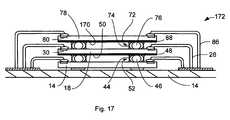
- a multiple die stack having three stacked diecan be made by providing a multiple-die assembly as in FIG. 6 , and mounting an additional die upon the second die by depositing adhesive/spacer material onto the second die generally as shown in FIG. 5 and placing the third die onto the deposits to make a three-die assembly as shown generally at 172 in FIG. 17 .
- FIG. 17a two die assembly as in FIG.
- the 6has a die 18 stacked over a die 14 , which is mounted onto a substrate 12 using an adhesive (in this instance, adhesive spots are used to attach the die 14 to the substrate 12 ).
- the die 18is separated from the die 14 by adhesive/spacer islands 52 , each including adhesive 44 and at least one spacer element 46 .
- a dielectric layer 48 applied onto the lower surface 50 of the die 18serves to prevent electrical shorting between the die 18 and wire bonds interconnecting the die 14 and the substrate 12 , and thereby allows for reduction of tolerances for the spacer dimension, as described above. Interconnection of the die 18 with the substrate 12 is made by wire bonds 26 connected to bond pads 30 on die 18 .
- deposits of adhesive/spacer materialincluding adhesive 74 and at least one spacer element 76 , are applied on the surface of die 18 , generally as described above with reference to FIGS. 3-5 , and then die 78 , having a dielectric layer 88 applied onto the lower surface 170 , is placed upon the adhesive/spacer material deposits.
- the resulting adhesive/spacer islands 72provide a sufficient between the die 78 and the die 18 equal to a design wire loop height for wire bonds 26 plus an allowance for manufacturing tolerance.
- Electrical interconnect between the die 78 and the substrateis then made, using a wire bonding tool to connect to bond pads 80 .
- further additional diecan be added to the stack. When the stack is complete, an encapsulating process is employed to complete the package and, where the package is made in an array of packages on a multipackage substrate, the packages are separated from one another by saw- or punch-singulation.
- the adhesive/spacer structuresare shown in FIGS. 6 and 17 as constituting islands having regular size and shape; according to the invention the islands may have any of various shapes and sizes, as described above with reference, for example, to FIGS. 9-11 and 13 - 16 .
- At least two die in the stackare separated by an adhesive/spacer structure; or, at least the lower die in the stack is separated from the substrate by an adhesive/spacer structure. All the die may be separated by spacers, at least two of them being separated by a adhesive/spacer structure; or, in some instances where one or more die is narrower than the die upon which it is stacked, no spacer may be required between those two die.
- either 14 or 18 , or both 14 and 18could constitute, rather than a die, a package including at least one die attached to and electrically connected to a substrate.
- a stacked semiconductor assemblyincludes a package stacked with a die, separated by an adhesive/spacer material generally as described above for stacked die assemblies.
- FIGS. 18 and 19illustrate examples 102 , 103 of such assemblies, in which an inverted package is stacked over a die.
- a lower, peripheral bonded die 142is mounted upon a substrate 112 , and bond pads on the die are electrically interconnected with bond pads on the substrate by wire bonds 120 .
- An adhesive/spacer structure 146is formed upon the die 142 including an adhesive and spacer elements arranged as discrete islands as described above with reference to adhesive/spacer structures 58 .
- An upper package 100is inverted and mounted upon the adhesive/spacer structure 146 , in substantially the same manner as the upper die 18 is mounted upon adhesive/spacer structure 52 in the stacked die assembly 51 , for example, of FIG. 6 .
- the upper package 100 in this exampleis a land grid array package, having a die 242 mounted onto a die attach side on upper package substrate 212 .
- Die 242 in this exampleis wire bonded to substrate 212 , and the die and wire bonds are enclosed in an encapsulation 217 .
- the package 100is inverted so that the land side of the substrate 212 faces away from the first die 142 and substrate 212 , and so that an upper surface of the encapsulation 217 faces toward the first die 142 and substrate 212 . In the orientation of FIG.
- the land side of the inverted upper package 212is upward-facing, and the upper package is electrically interconnected with the bottom substrate 212 by wire bonds between bond pads on the land side of the upper package substrate 212 and bond pads on the upward-facing side of the lower substrate 112 .
- the assemblyis then encapsulated (not shown in FIG. 18 ) to form a package, substantially as the stacked die assembly 51 of FIG. 6 is encapsulated to form the package 56 of FIG. 12 .
- Solder balls 118are mounted onto pads on the downward-facing side of the substrate 112 , for interconnection of the package to, for example, a motherboard.
- two (or more) diemay be stacked using an adhesive/spacer structure over one another on a lower substrate, and a package may be stacked over the uppermost one of the stacked die, using an adhesive/spacer structure, as shown by way of example in FIG. 19 .
- a die 142is mounted onto a lower substrate 112
- a die 144is stacked over the die 142 , and separated from it by an adhesive/spacer structure 246 as described above for stacked die assemblies.
- Die 142 and 144are electrically interconnected with substrate 112 by wire bonds 220 .
- An inverted package 100is mounted over the stacked die 142 , 144 , separated by the die 144 by and adhesive/spacer structure 246 , as described above with reference to FIG. 18 .
- the spacers, between the die, and between the die and the inverted packagemay be an island adhesive/spacer structure as described above with reference to stacked die assemblies.
- any of a variety of packagesmay be stacked over the die in assemblies according to these embodiments of the invention.
- Stacked multi-package modules having inverted upper packagesare described in U.S. patent application Ser. No. 10/681,572; and examples of suitable upper inverted package types are described therein. These include, for example, besides land grid array packages as illustrated in FIGS. 18 and 19 , bump chip carrier packages; and the upper package may include more than one die.
- the upper package encapsulanthas a generally planar surface that contacts the adhesive/spacer structure, that surface (termed the “second” surface) is itself electrically nonconductive and application of an additional insulating layer (as layer 48 in FIG. 6 ) may be optional in such embodiments.
- the second surface of the upper packageis an electrically conductive material (such as a metal heat spreader, for example) or includes exposed electrically conductive areas or elements
- an insulating layer 48should be applied, as described above with reference for example to FIG. 6 .
- a stacked semiconductor assemblyin which a stacked semiconductor assembly includes a package stacked with a die, separated by an adhesive/spacer material generally as described above for stacked die assemblies, the upper package is not inverted.
- FIGS. 20 and 21illustrate examples 104 , 105 of such assemblies.
- a lower, peripheral bonded die 142is mounted upon a substrate 112 , and bond pads on the die are electrically interconnected with bond pads on the substrate by wire bonds 120 .
- An adhesive/spacer structure 146is formed upon the die 142 including an adhesive and spacer elements as described above with reference to adhesive/spacer structure 52 .
- An upper package 400is inverted and mounted upon the adhesive/spacer structure 146 , in substantially the same manner as the upper die 18 is mounted upon adhesive/spacer structure 52 in the stacked die assembly 51 , for example, of FIG. 6 .
- the upper package 400 in this exampleis a land grid array package, having a die 442 mounted onto a die attach side on upper package substrate 412 .
- Die 442 in this exampleis wire bonded to substrate 412 , and the die and wire bonds are enclosed in a mold cap 417 .
- the package 400is oriented so that the land side of the substrate 412 faces toward the first die 142 and substrate 212 , and so that the land side of the upper package substrate 412 faces toward the first die 142 and substrate 212 . In the orientation of FIG.
- the land side of the inverted upper package 412is downward-facing, and the upper package is electrically interconnected with the bottom substrate 112 by wire bonds between bond pads on the upward-facing (die attach) side of the upper package substrate 412 and bond pads on the upward-facing side of the lower substrate 112 .
- the assemblyis then encapsulated (not shown in FIG. 20 ) to form a package, substantially as the stacked die assembly 51 of FIG. 6 is encapsulated to form the package 56 of FIG. 12 .
- Solder balls 118are mounted onto pads on the downward-facing side of the substrate 112 , for interconnection of the package to, for example, a motherboard.
- two (or more) diemay be stacked using an adhesive/spacer structure over one another on a lower substrate, and a package may be stacked over the uppermost one of the stacked die, using an adhesive/spacer structure, as shown by way of example in FIG. 21 .
- a die 142is mounted onto a lower substrate 112
- a die 144is stacked over the die 142 , and separated from it by an adhesive/spacer structure 246 as described above for stacked die assemblies.
- Die 142 and 144are electrically interconnected with substrate 112 by wire bonds 220 .
- An inverted package 100is mounted over the stacked die 142 , 144 , separated by the die 144 by and adhesive/spacer structure 246 , as described above with reference to FIG. 19 .
- the spacers, between the die, and between the die and the inverted packagemay be an adhesive/spacer structure as described above with reference to stacked die assemblies.
- any of a variety of packagesmay be stacked over the die in assemblies according to these embodiments of the invention.
- Stacked multi-package modules suitable upper packagesare described in U.S. patent application Ser. Nos. 10/632,549; 10/632,568; 10/632,551; 10/632,552; 10/632,553; and 10/632,550; and examples of suitable upper package types are described therein. These include, for example, besides land grid array packages as illustrated in FIGS. 20 and 21 , bump chip carrier packages, and flip chip packages; and the upper package may include more than one die. Where the downward-facing surface of the upper package (“second” surface) had electrically conductive elements or areas, application of an additional insulating layer (as layer 48 in FIG.
- This additional insulating layermay be applied as a film to the land side of the upper package substrate, and voids between the film and the substrate surface removed by heating at low pressure, according to techniques known in the art.
- both the element 18 and the element 14may be a package, comprising a die mounted onto and electrically connected with a substrate.
- Other devicesmay be stacked over the first die, and separated therefrom by an adhesive/spacer structure as described above, and provided with an insulating layer as appropriate.
- a metal heat spreadermay be stacked upon an adhesive/spacer structure over the first die in place of the upper die or upper package in the descriptions above.
- the assemblies and packages according to the inventioncan be useful in any of a variety of products, such as for example computers, mobile telecommunications devices, personal digital assistance devices, media storage devices, particularly portable cameras and audio and video equipment.
Landscapes
- Engineering & Computer Science (AREA)
- Microelectronics & Electronic Packaging (AREA)
- Power Engineering (AREA)
- Computer Hardware Design (AREA)
- Manufacturing & Machinery (AREA)
- Physics & Mathematics (AREA)
- Condensed Matter Physics & Semiconductors (AREA)
- General Physics & Mathematics (AREA)
- Die Bonding (AREA)
Abstract
Description
Claims (13)
Priority Applications (3)
| Application Number | Priority Date | Filing Date | Title |
|---|---|---|---|
| US11/134,845US8552551B2 (en) | 2004-05-24 | 2005-05-20 | Adhesive/spacer island structure for stacking over wire bonded die |
| TW094117103ATWI445157B (en) | 2004-05-24 | 2005-05-24 | Adhesive/gap structure of multi-die package |
| TW102116249ATW201334151A (en) | 2004-05-24 | 2005-05-24 | Adhesive/spacer island structure for multiple die package |
Applications Claiming Priority (4)
| Application Number | Priority Date | Filing Date | Title |
|---|---|---|---|
| US57390304P | 2004-05-24 | 2004-05-24 | |
| US57395604P | 2004-05-24 | 2004-05-24 | |
| US10/969,116US20050258527A1 (en) | 2004-05-24 | 2004-10-20 | Adhesive/spacer island structure for multiple die package |
| US11/134,845US8552551B2 (en) | 2004-05-24 | 2005-05-20 | Adhesive/spacer island structure for stacking over wire bonded die |
Related Parent Applications (1)
| Application Number | Title | Priority Date | Filing Date |
|---|---|---|---|
| US10/969,116Continuation-In-PartUS20050258527A1 (en) | 2004-05-24 | 2004-10-20 | Adhesive/spacer island structure for multiple die package |
Publications (2)
| Publication Number | Publication Date |
|---|---|
| US20050269676A1 US20050269676A1 (en) | 2005-12-08 |
| US8552551B2true US8552551B2 (en) | 2013-10-08 |
Family
ID=46304595
Family Applications (1)
| Application Number | Title | Priority Date | Filing Date |
|---|---|---|---|
| US11/134,845Active2027-03-14US8552551B2 (en) | 2004-05-24 | 2005-05-20 | Adhesive/spacer island structure for stacking over wire bonded die |
Country Status (1)
| Country | Link |
|---|---|
| US (1) | US8552551B2 (en) |
Cited By (1)
| Publication number | Priority date | Publication date | Assignee | Title |
|---|---|---|---|---|
| US20150187713A1 (en)* | 2006-06-29 | 2015-07-02 | Intel Corporation | Apparatus, system, and method for wireless connection in integrated circuit packages |
Families Citing this family (9)
| Publication number | Priority date | Publication date | Assignee | Title |
|---|---|---|---|---|
| AU2003298595A1 (en)* | 2002-10-08 | 2004-05-04 | Chippac, Inc. | Semiconductor stacked multi-package module having inverted second package |
| US20050110126A1 (en)* | 2003-11-25 | 2005-05-26 | Kai-Chiang Wu | Chip adhesive |
| US7425464B2 (en)* | 2006-03-10 | 2008-09-16 | Freescale Semiconductor, Inc. | Semiconductor device packaging |
| US8134227B2 (en)* | 2007-03-30 | 2012-03-13 | Stats Chippac Ltd. | Stacked integrated circuit package system with conductive spacer |
| US7683477B2 (en)* | 2007-06-26 | 2010-03-23 | Infineon Technologies Ag | Semiconductor device including semiconductor chips having contact elements |
| JP5543084B2 (en)* | 2008-06-24 | 2014-07-09 | ピーエスフォー ルクスコ エスエイアールエル | Manufacturing method of semiconductor device |
| JP2011077108A (en)* | 2009-09-29 | 2011-04-14 | Elpida Memory Inc | Semiconductor device |
| KR102511832B1 (en)* | 2016-08-26 | 2023-03-20 | 삼성전자주식회사 | Semiconductor package device |
| JP6319477B1 (en)* | 2017-02-14 | 2018-05-09 | 日本電気株式会社 | Module, module manufacturing method, package |
Citations (142)
| Publication number | Priority date | Publication date | Assignee | Title |
|---|---|---|---|---|
| US5140404A (en) | 1990-10-24 | 1992-08-18 | Micron Technology, Inc. | Semiconductor device manufactured by a method for attaching a semiconductor die to a leadframe using a thermoplastic covered carrier tape |
| US5218229A (en) | 1991-08-30 | 1993-06-08 | Micron Technology, Inc. | Inset die lead frame configuration lead frame for a semiconductor device having means for improved busing and die-lead frame attachment |
| US5222014A (en) | 1992-03-02 | 1993-06-22 | Motorola, Inc. | Three-dimensional multi-chip pad array carrier |
| US5229960A (en) | 1990-12-05 | 1993-07-20 | Matra Marconi Space France | Solid state memory modules and memory devices including such modules |
| US5323060A (en) | 1993-06-02 | 1994-06-21 | Micron Semiconductor, Inc. | Multichip module having a stacked chip arrangement |
| US5340771A (en) | 1993-03-18 | 1994-08-23 | Lsi Logic Corporation | Techniques for providing high I/O count connections to semiconductor dies |
| US5372883A (en) | 1990-03-20 | 1994-12-13 | Staystik, Inc. | Die attach adhesive film, application method and devices incorporating the same |
| US5373189A (en) | 1992-08-13 | 1994-12-13 | Commissariate A L'energie Atomique | Three-dimensional multichip module |
| US5436203A (en) | 1994-07-05 | 1995-07-25 | Motorola, Inc. | Shielded liquid encapsulated semiconductor device and method for making the same |
| US5444296A (en) | 1993-11-22 | 1995-08-22 | Sun Microsystems, Inc. | Ball grid array packages for high speed applications |
| US5495398A (en) | 1992-05-22 | 1996-02-27 | National Semiconductor Corporation | Stacked multi-chip modules and method of manufacturing |
| US5550711A (en) | 1990-08-01 | 1996-08-27 | Staktek Corporation | Ultra high density integrated circuit packages |
| US5652185A (en) | 1995-04-07 | 1997-07-29 | National Semiconductor Corporation | Maximized substrate design for grid array based assemblies |
| US5744863A (en) | 1994-07-11 | 1998-04-28 | International Business Machines Corporation | Chip carrier modules with heat sinks attached by flexible-epoxy |
| US5753358A (en)* | 1994-08-25 | 1998-05-19 | W. L. Gore & Associates, Inc. | Adhisive-filler polymer film composite |
| US5776799A (en) | 1996-11-08 | 1998-07-07 | Samsung Electronics Co., Ltd. | Lead-on-chip type semiconductor chip package using an adhesive deposited on chip active surfaces at a wafer level and method for manufacturing same |
| US5898219A (en) | 1997-04-02 | 1999-04-27 | Intel Corporation | Custom corner attach heat sink design for a plastic ball grid array integrated circuit package |
| US5899705A (en) | 1997-11-20 | 1999-05-04 | Akram; Salman | Stacked leads-over chip multi-chip module |
| US5903049A (en) | 1997-10-29 | 1999-05-11 | Mitsubishi Denki Kabushiki Kaisha | Semiconductor module comprising semiconductor packages |
| US5945733A (en) | 1994-11-14 | 1999-08-31 | Micron Technology, Inc. | Structure for attaching a semiconductor wafer section to a support |
| US5977640A (en) | 1998-06-26 | 1999-11-02 | International Business Machines Corporation | Highly integrated chip-on-chip packaging |
| US5982633A (en) | 1997-08-20 | 1999-11-09 | Compaq Computer Corporation | Opposed ball grid array mounting |
| US5994166A (en) | 1997-03-10 | 1999-11-30 | Micron Technology, Inc. | Method of constructing stacked packages |
| US6025648A (en) | 1997-04-17 | 2000-02-15 | Nec Corporation | Shock resistant semiconductor device and method for producing same |
| US6034875A (en) | 1998-06-17 | 2000-03-07 | International Business Machines Corporation | Cooling structure for electronic components |
| US6075289A (en) | 1996-10-24 | 2000-06-13 | Tessera, Inc. | Thermally enhanced packaged semiconductor assemblies |
| US6118176A (en) | 1999-04-26 | 2000-09-12 | Advanced Semiconductor Engineering, Inc. | Stacked chip assembly utilizing a lead frame |
| US6133626A (en) | 1997-10-10 | 2000-10-17 | Gennum Corporation | Three dimensional packaging configuration for multi-chip module assembly |
| US6157080A (en) | 1997-11-06 | 2000-12-05 | Sharp Kabushiki Kaisha | Semiconductor device using a chip scale package |
| US6177729B1 (en)* | 1999-04-03 | 2001-01-23 | International Business Machines Corporation | Rolling ball connector |
| US6201266B1 (en) | 1999-07-01 | 2001-03-13 | Oki Electric Industry Co., Ltd. | Semiconductor device and method for manufacturing the same |
| US6201302B1 (en) | 1998-12-31 | 2001-03-13 | Sampo Semiconductor Corporation | Semiconductor package having multi-dies |
| US6238946B1 (en)* | 1999-08-17 | 2001-05-29 | International Business Machines Corporation | Process for fabricating single crystal resonant devices that are compatible with integrated circuit processing |
| US6238949B1 (en) | 1999-06-18 | 2001-05-29 | National Semiconductor Corporation | Method and apparatus for forming a plastic chip on chip package module |
| US6265766B1 (en) | 1995-12-19 | 2001-07-24 | Micron Technology, Inc. | Flip chip adaptor package for bare die |
| US6265763B1 (en) | 2000-03-14 | 2001-07-24 | Siliconware Precision Industries Co., Ltd. | Multi-chip integrated circuit package structure for central pad chip |
| US6274930B1 (en) | 1999-08-17 | 2001-08-14 | Micron Technology, Inc. | Multi-chip module with stacked dice |
| JP2001223326A (en) | 2000-02-09 | 2001-08-17 | Hitachi Ltd | Semiconductor device |
| US6316838B1 (en) | 1999-10-29 | 2001-11-13 | Fujitsu Limited | Semiconductor device |
| US6333552B1 (en) | 1998-08-07 | 2001-12-25 | Sharp Kabushiki Kaisha | Millimeter wave semiconductor device |
| US6333562B1 (en) | 2000-07-13 | 2001-12-25 | Advanced Semiconductor Engineering, Inc. | Multichip module having stacked chip arrangement |
| US6340846B1 (en) | 2000-12-06 | 2002-01-22 | Amkor Technology, Inc. | Making semiconductor packages with stacked dies and reinforced wire bonds |
| US6351028B1 (en) | 1999-02-08 | 2002-02-26 | Micron Technology, Inc. | Multiple die stack apparatus employing T-shaped interposer elements |
| US6376904B1 (en) | 1999-12-23 | 2002-04-23 | Rambus Inc. | Redistributed bond pads in stacked integrated circuit die package |
| US6388313B1 (en) | 2001-01-30 | 2002-05-14 | Siliconware Precision Industries Co., Ltd. | Multi-chip module |
| US6400007B1 (en) | 2001-04-16 | 2002-06-04 | Kingpak Technology Inc. | Stacked structure of semiconductor means and method for manufacturing the same |
| US6407456B1 (en) | 1996-02-20 | 2002-06-18 | Micron Technology, Inc. | Multi-chip device utilizing a flip chip and wire bond assembly |
| US6413798B2 (en) | 1998-01-18 | 2002-07-02 | Kabushiki Kaisha Toshiba | Package having very thin semiconductor chip, multichip module assembled by the package, and method for manufacturing the same |
| US6414381B1 (en) | 1999-03-15 | 2002-07-02 | Fujitsu Media Devices Limited | Interposer for separating stacked semiconductor chips mounted on a multi-layer printed circuit board |
| US6424050B1 (en) | 1999-09-22 | 2002-07-23 | Seiko Epson Corporation | Semiconductor device |
| US20020096755A1 (en) | 2001-01-24 | 2002-07-25 | Yasuki Fukui | Semiconductor device |
| US6436732B2 (en) | 1997-08-21 | 2002-08-20 | Micron Technology, Inc. | Apparatus for applying viscous materials to a lead frame |
| US6441496B1 (en)* | 2000-11-22 | 2002-08-27 | Wen Chuan Chen | Structure of stacked integrated circuits |
| US6445064B1 (en) | 2001-02-06 | 2002-09-03 | Mitsubishi Denki Kabushiki Kaisha | Semiconductor device |
| US20020130404A1 (en) | 2001-03-19 | 2002-09-19 | Toshihiro Ushijima | Semiconductor module in which plural semiconductor chips are enclosed in one package |
| US6462421B1 (en) | 2000-04-10 | 2002-10-08 | Advanced Semicondcutor Engineering, Inc. | Multichip module |
| US6472732B1 (en) | 1999-10-25 | 2002-10-29 | Oki Electric Industry Co., Ltd. | BGA package and method for fabricating the same |
| US6472741B1 (en) | 2001-07-14 | 2002-10-29 | Siliconware Precision Industries Co., Ltd. | Thermally-enhanced stacked-die ball grid array semiconductor package and method of fabricating the same |
| US6472758B1 (en)* | 2000-07-20 | 2002-10-29 | Amkor Technology, Inc. | Semiconductor package including stacked semiconductor dies and bond wires |
| US6489676B2 (en) | 2000-12-04 | 2002-12-03 | Fujitsu Limited | Semiconductor device having an interconnecting post formed on an interposer within a sealing resin |
| US6492726B1 (en) | 2000-09-22 | 2002-12-10 | Chartered Semiconductor Manufacturing Ltd. | Chip scale packaging with multi-layer flip chip arrangement and ball grid array interconnection |
| US6501165B1 (en) | 1998-06-05 | 2002-12-31 | Micron Technology, Inc. | Stackable semiconductor package having conductive layer and insulating layers and method of fabrication |
| US6503821B2 (en) | 1998-10-21 | 2003-01-07 | International Business Machines Corporation | Integrated circuit chip carrier assembly |
| US20030038374A1 (en) | 2001-08-27 | 2003-02-27 | Shim Jong Bo | Multi-chip package (MCP) with spacer |
| US20030038357A1 (en) | 2001-08-24 | 2003-02-27 | Derderian James M. | Spacer for semiconductor devices, semiconductor devices and assemblies including the spacer, and methods |
| US20030054162A1 (en) | 2001-09-17 | 2003-03-20 | Watson Michael John | Adhesives for semiconductor applications efficient processes for producing such devices and the devices per se produced by the efficient processes |
| US6538319B2 (en) | 1997-09-02 | 2003-03-25 | Oki Electric Industry Co., Ltd. | Semiconductor device |
| US6545366B2 (en) | 2001-01-11 | 2003-04-08 | Mitsubishi Denki Kabushiki Kaisha | Multiple chip package semiconductor device |
| US6545365B2 (en) | 2000-04-26 | 2003-04-08 | Mitsubishi Denki Kabushiki Kaisha | Resin-sealed chip stack type semiconductor device |
| US6552423B2 (en) | 2000-02-18 | 2003-04-22 | Samsung Electronics Co., Ltd. | Higher-density memory card |
| US6555902B2 (en) | 2000-07-17 | 2003-04-29 | Siliconware Precision Industries Co., Ltd. | Multiple stacked-chip packaging structure |
| US6569709B2 (en)* | 2001-10-15 | 2003-05-27 | Micron Technology, Inc. | Assemblies including stacked semiconductor devices separated a distance defined by adhesive material interposed therebetween, packages including the assemblies, and methods |
| US6570249B1 (en) | 2001-12-24 | 2003-05-27 | Siliconware Precision Industries Co., Ltd. | Semiconductor package |
| US20030113952A1 (en) | 2001-12-19 | 2003-06-19 | Mahesh Sambasivam | Underfill materials dispensed in a flip chip package by way of a through hole |
| US6590281B2 (en) | 2001-11-15 | 2003-07-08 | Siliconware Precision Industries Co., Ltd. | Crack-preventive semiconductor package |
| US6593662B1 (en) | 2000-06-16 | 2003-07-15 | Siliconware Precision Industries Co., Ltd. | Stacked-die package structure |
| US6593647B2 (en) | 2001-06-15 | 2003-07-15 | Oki Electric Industry Co., Ltd. | Semiconductor device |
| US6593648B2 (en) | 2000-08-31 | 2003-07-15 | Seiko Epson Corporation | Semiconductor device and method of making the same, circuit board and electronic equipment |
| US6599779B2 (en) | 2001-09-24 | 2003-07-29 | St Assembly Test Service Ltd. | PBGA substrate for anchoring heat sink |
| US20030141582A1 (en) | 2002-01-25 | 2003-07-31 | Yang Chaur-Chin | Stack type flip-chip package |
| US20030153134A1 (en) | 1998-06-01 | 2003-08-14 | Youichi Kawata | Semiconductor device, and a method of producing semiconductor device |
| US6607937B1 (en) | 2000-08-23 | 2003-08-19 | Micron Technology, Inc. | Stacked microelectronic dies and methods for stacking microelectronic dies |
| US6611063B1 (en) | 1999-09-16 | 2003-08-26 | Nec Electronics Corporation | Resin-encapsulated semiconductor device |
| US6620651B2 (en) | 2001-10-23 | 2003-09-16 | National Starch And Chemical Investment Holding Corporation | Adhesive wafers for die attach application |
| US6621169B2 (en) | 2000-09-04 | 2003-09-16 | Fujitsu Limited | Stacked semiconductor device and method of producing the same |
| US6621172B2 (en) | 1999-09-03 | 2003-09-16 | Seiko Epson Corporation | Semiconductor device and method of fabricating the same, circuit board, and electronic equipment |
| US20030178710A1 (en) | 2002-03-21 | 2003-09-25 | Samsung Electronics Co., Ltd. | Semiconductor chip stack structure and method for forming the same |
| US6650009B2 (en) | 2000-07-18 | 2003-11-18 | Siliconware Precision Industries Co., Ltd. | Structure of a multi chip module having stacked chips |
| US6649448B2 (en) | 2000-10-05 | 2003-11-18 | Hitachi, Ltd. | Method of manufacturing a semiconductor device having flexible wiring substrate |
| US6660560B2 (en) | 2001-09-10 | 2003-12-09 | Delphi Technologies, Inc. | No-flow underfill material and underfill method for flip chip devices |
| US20040016939A1 (en) | 2002-07-26 | 2004-01-29 | Masayuki Akiba | Encapsulation of a stack of semiconductor dice |
| US6690089B2 (en) | 2002-05-15 | 2004-02-10 | Oki Electric Industry Co., Ltd. | Semiconductor device having multi-chip package |
| US20040026768A1 (en) | 2002-08-08 | 2004-02-12 | Taar Reginald T. | Semiconductor dice with edge cavities |
| US20040039127A1 (en) | 2002-08-26 | 2004-02-26 | Satoru Amou | Electronic device using low dielectric loss tangent insulators for high frequency signals |
| US6700178B2 (en) | 2001-03-09 | 2004-03-02 | Advanced Semiconductor Engineering, Inc. | Package of a chip with beveled edges |
| US6706557B2 (en) | 2001-09-21 | 2004-03-16 | Micron Technology, Inc. | Method of fabricating stacked die configurations utilizing redistribution bond pads |
| US6710455B2 (en) | 2001-08-30 | 2004-03-23 | Infineon Technologies Ag | Electronic component with at least two stacked semiconductor chips and method for fabricating the electronic component |
| US20040061213A1 (en) | 2002-09-17 | 2004-04-01 | Chippac, Inc. | Semiconductor multi-package module having package stacked over die-up flip chip ball grid array package and having wire bond interconnect between stacked packages |
| US6734539B2 (en) | 2000-12-27 | 2004-05-11 | Lucent Technologies Inc. | Stacked module package |
| US6734552B2 (en) | 2001-07-11 | 2004-05-11 | Asat Limited | Enhanced thermal dissipation integrated circuit package |
| US6737750B1 (en) | 2001-12-07 | 2004-05-18 | Amkor Technology, Inc. | Structures for improving heat dissipation in stacked semiconductor packages |
| US6746894B2 (en) | 2001-03-30 | 2004-06-08 | Micron Technology, Inc. | Ball grid array interposer, packages and methods |
| US6747361B2 (en) | 2000-07-26 | 2004-06-08 | Nec Electronics Corporation | Semiconductor device and packaging method thereof |
| US6753613B2 (en)* | 2002-03-13 | 2004-06-22 | Intel Corporation | Stacked dice standoffs |
| US6762488B2 (en) | 2002-03-19 | 2004-07-13 | Nec Electronics Corporation | Light thin stacked package semiconductor device and process for fabrication thereof |
| US6777819B2 (en) | 2000-12-20 | 2004-08-17 | Siliconware Precision Industries Co., Ltd. | Semiconductor package with flash-proof device |
| US6784555B2 (en)* | 2001-09-17 | 2004-08-31 | Dow Corning Corporation | Die attach adhesives for semiconductor applications utilizing a polymeric base material with inorganic insulator particles of various sizes |
| US6787916B2 (en) | 2001-09-13 | 2004-09-07 | Tru-Si Technologies, Inc. | Structures having a substrate with a cavity and having an integrated circuit bonded to a contact pad located in the cavity |
| US6787915B2 (en) | 2001-03-05 | 2004-09-07 | Oki Electric Industry Co., Ltd. | Rearrangement sheet, semiconductor device and method of manufacturing thereof |
| US6794749B2 (en) | 1999-08-31 | 2004-09-21 | Micron Technology, Inc. | Chip package with grease heat sink |
| US20040195667A1 (en) | 2003-04-04 | 2004-10-07 | Chippac, Inc | Semiconductor multipackage module including processor and memory package assemblies |
| US20040212096A1 (en) | 2003-04-23 | 2004-10-28 | Advanced Semiconductor Engineering, Inc. | Multi-chips stacked package |
| US6818980B1 (en) | 2003-05-07 | 2004-11-16 | Asat Ltd. | Stacked semiconductor package and method of manufacturing the same |
| US6828665B2 (en) | 2002-10-18 | 2004-12-07 | Siliconware Precision Industries Co., Ltd. | Module device of stacked semiconductor packages and method for fabricating the same |
| US6833287B1 (en) | 2003-06-16 | 2004-12-21 | St Assembly Test Services Inc. | System for semiconductor package with stacked dies |
| US6835598B2 (en) | 2002-07-24 | 2004-12-28 | Samsung Electronics Co., Ltd. | Stacked semiconductor module and method of manufacturing the same |
| US6838761B2 (en) | 2002-09-17 | 2005-01-04 | Chippac, Inc. | Semiconductor multi-package module having wire bond interconnect between stacked packages and having electrical shield |
| US6858468B2 (en)* | 2000-05-09 | 2005-02-22 | National Semiconductor Corporation | Techniques for joining an opto-electronic module to a semiconductor package |
| US6864566B2 (en) | 2001-08-21 | 2005-03-08 | Samsung Electronics Co., Ltd. | Duel die package |
| US6882057B2 (en) | 2003-06-25 | 2005-04-19 | Via Technologies, Inc. | Quad flat no-lead chip carrier |
| US6885093B2 (en) | 2002-02-28 | 2005-04-26 | Freescale Semiconductor, Inc. | Stacked die semiconductor device |
| US20050090050A1 (en)* | 2003-01-23 | 2005-04-28 | St Assembly Test Services Ltd. | Stacked semiconductor packages |
| US6890798B2 (en) | 1999-06-08 | 2005-05-10 | Intel Corporation | Stacked chip packaging |
| US20050106779A1 (en) | 2003-03-11 | 2005-05-19 | Bolken Todd O. | Techniques for packaging multiple device components |
| US6900528B2 (en) | 2001-06-21 | 2005-05-31 | Micron Technology, Inc. | Stacked mass storage flash memory package |
| US6906416B2 (en) | 2002-10-08 | 2005-06-14 | Chippac, Inc. | Semiconductor multi-package module having inverted second package stacked over die-up flip-chip ball grid array (BGA) package |
| US6906415B2 (en) | 2002-06-27 | 2005-06-14 | Micron Technology, Inc. | Semiconductor device assemblies and packages including multiple semiconductor devices and methods |
| US6919627B2 (en) | 2002-06-04 | 2005-07-19 | Siliconware Precision Industries Co., Ltd. | Multichip module |
| US6930378B1 (en) | 2003-11-10 | 2005-08-16 | Amkor Technology, Inc. | Stacked semiconductor die assembly having at least one support |
| US6930396B2 (en) | 2002-04-05 | 2005-08-16 | Nec Electronics Corporation | Semiconductor device and method for manufacturing the same |
| US6951982B2 (en) | 2002-11-22 | 2005-10-04 | Micron Technology, Inc. | Packaged microelectronic component assemblies |
| US20050224959A1 (en) | 2004-04-01 | 2005-10-13 | Chippac, Inc | Die with discrete spacers and die spacing method |
| US20050243268A1 (en) | 2002-09-19 | 2005-11-03 | Koninklijke Philips Electronics N.V. | Pair of substrates spaced from each other by spacers having a pre-determined pattern and method of making thereof |
| US6972481B2 (en) | 2002-09-17 | 2005-12-06 | Chippac, Inc. | Semiconductor multi-package module including stacked-die package and having wire bond interconnect between stacked packages |
| US20060043556A1 (en) | 2004-08-25 | 2006-03-02 | Chao-Yuan Su | Stacked packaging methods and structures |
| US7034388B2 (en) | 2002-01-25 | 2006-04-25 | Advanced Semiconductor Engineering, Inc. | Stack type flip-chip package |
| US7053476B2 (en) | 2002-09-17 | 2006-05-30 | Chippac, Inc. | Semiconductor multi-package module having package stacked over die-down flip chip ball grid array package and having wire bond interconnect between stacked packages |
| US7064426B2 (en) | 2002-09-17 | 2006-06-20 | Chippac, Inc. | Semiconductor multi-package module having wire bond interconnect between stacked packages |
| US20060138631A1 (en) | 2003-12-31 | 2006-06-29 | Advanced Semiconductor Engineering, Inc. | Multi-chip package structure |
| US7081678B2 (en) | 2003-04-04 | 2006-07-25 | Advanced Semiconductor Engineering Inc. | Multi-chip package combining wire-bonding and flip-chip configuration |
| US20060189033A1 (en) | 2005-02-04 | 2006-08-24 | Stats Chippac Ltd. | Integrated circuit package-in-package system |
| US20060197209A1 (en) | 2005-02-10 | 2006-09-07 | Stats Chippac Ltd. | Stacked integrated circuits package system with dense routability and high thermal conductivity |
- 2005
- 2005-05-20USUS11/134,845patent/US8552551B2/enactiveActive
Patent Citations (159)
| Publication number | Priority date | Publication date | Assignee | Title |
|---|---|---|---|---|
| US5372883A (en) | 1990-03-20 | 1994-12-13 | Staystik, Inc. | Die attach adhesive film, application method and devices incorporating the same |
| US5550711A (en) | 1990-08-01 | 1996-08-27 | Staktek Corporation | Ultra high density integrated circuit packages |
| US5140404A (en) | 1990-10-24 | 1992-08-18 | Micron Technology, Inc. | Semiconductor device manufactured by a method for attaching a semiconductor die to a leadframe using a thermoplastic covered carrier tape |
| US5229960A (en) | 1990-12-05 | 1993-07-20 | Matra Marconi Space France | Solid state memory modules and memory devices including such modules |
| US5218229A (en) | 1991-08-30 | 1993-06-08 | Micron Technology, Inc. | Inset die lead frame configuration lead frame for a semiconductor device having means for improved busing and die-lead frame attachment |
| US5222014A (en) | 1992-03-02 | 1993-06-22 | Motorola, Inc. | Three-dimensional multi-chip pad array carrier |
| US5495398A (en) | 1992-05-22 | 1996-02-27 | National Semiconductor Corporation | Stacked multi-chip modules and method of manufacturing |
| US5373189A (en) | 1992-08-13 | 1994-12-13 | Commissariate A L'energie Atomique | Three-dimensional multichip module |
| US5340771A (en) | 1993-03-18 | 1994-08-23 | Lsi Logic Corporation | Techniques for providing high I/O count connections to semiconductor dies |
| US5323060A (en) | 1993-06-02 | 1994-06-21 | Micron Semiconductor, Inc. | Multichip module having a stacked chip arrangement |
| US5444296A (en) | 1993-11-22 | 1995-08-22 | Sun Microsystems, Inc. | Ball grid array packages for high speed applications |
| US5436203A (en) | 1994-07-05 | 1995-07-25 | Motorola, Inc. | Shielded liquid encapsulated semiconductor device and method for making the same |
| US5744863A (en) | 1994-07-11 | 1998-04-28 | International Business Machines Corporation | Chip carrier modules with heat sinks attached by flexible-epoxy |
| US5753358A (en)* | 1994-08-25 | 1998-05-19 | W. L. Gore & Associates, Inc. | Adhisive-filler polymer film composite |
| US5945733A (en) | 1994-11-14 | 1999-08-31 | Micron Technology, Inc. | Structure for attaching a semiconductor wafer section to a support |
| US5652185A (en) | 1995-04-07 | 1997-07-29 | National Semiconductor Corporation | Maximized substrate design for grid array based assemblies |
| US6265766B1 (en) | 1995-12-19 | 2001-07-24 | Micron Technology, Inc. | Flip chip adaptor package for bare die |
| US6667556B2 (en) | 1995-12-19 | 2003-12-23 | Micron Technology, Inc. | Flip chip adaptor package for bare die |
| US6512303B2 (en) | 1995-12-19 | 2003-01-28 | Micron Technology, Inc. | Flip chip adaptor package for bare die |
| US6407456B1 (en) | 1996-02-20 | 2002-06-18 | Micron Technology, Inc. | Multi-chip device utilizing a flip chip and wire bond assembly |
| US6075289A (en) | 1996-10-24 | 2000-06-13 | Tessera, Inc. | Thermally enhanced packaged semiconductor assemblies |
| US5776799A (en) | 1996-11-08 | 1998-07-07 | Samsung Electronics Co., Ltd. | Lead-on-chip type semiconductor chip package using an adhesive deposited on chip active surfaces at a wafer level and method for manufacturing same |
| US5994166A (en) | 1997-03-10 | 1999-11-30 | Micron Technology, Inc. | Method of constructing stacked packages |
| US6583503B2 (en) | 1997-03-10 | 2003-06-24 | Micron Technology, Inc. | Semiconductor package with stacked substrates and multiple semiconductor dice |
| US5898219A (en) | 1997-04-02 | 1999-04-27 | Intel Corporation | Custom corner attach heat sink design for a plastic ball grid array integrated circuit package |
| US6025648A (en) | 1997-04-17 | 2000-02-15 | Nec Corporation | Shock resistant semiconductor device and method for producing same |
| US5982633A (en) | 1997-08-20 | 1999-11-09 | Compaq Computer Corporation | Opposed ball grid array mounting |
| US6436732B2 (en) | 1997-08-21 | 2002-08-20 | Micron Technology, Inc. | Apparatus for applying viscous materials to a lead frame |
| US6538319B2 (en) | 1997-09-02 | 2003-03-25 | Oki Electric Industry Co., Ltd. | Semiconductor device |
| US6133626A (en) | 1997-10-10 | 2000-10-17 | Gennum Corporation | Three dimensional packaging configuration for multi-chip module assembly |
| US5903049A (en) | 1997-10-29 | 1999-05-11 | Mitsubishi Denki Kabushiki Kaisha | Semiconductor module comprising semiconductor packages |
| US6157080A (en) | 1997-11-06 | 2000-12-05 | Sharp Kabushiki Kaisha | Semiconductor device using a chip scale package |
| US5899705A (en) | 1997-11-20 | 1999-05-04 | Akram; Salman | Stacked leads-over chip multi-chip module |
| US6413798B2 (en) | 1998-01-18 | 2002-07-02 | Kabushiki Kaisha Toshiba | Package having very thin semiconductor chip, multichip module assembled by the package, and method for manufacturing the same |
| US20030153134A1 (en) | 1998-06-01 | 2003-08-14 | Youichi Kawata | Semiconductor device, and a method of producing semiconductor device |
| US6501165B1 (en) | 1998-06-05 | 2002-12-31 | Micron Technology, Inc. | Stackable semiconductor package having conductive layer and insulating layers and method of fabrication |
| US6034875A (en) | 1998-06-17 | 2000-03-07 | International Business Machines Corporation | Cooling structure for electronic components |
| US5977640A (en) | 1998-06-26 | 1999-11-02 | International Business Machines Corporation | Highly integrated chip-on-chip packaging |
| US6333552B1 (en) | 1998-08-07 | 2001-12-25 | Sharp Kabushiki Kaisha | Millimeter wave semiconductor device |
| US6503821B2 (en) | 1998-10-21 | 2003-01-07 | International Business Machines Corporation | Integrated circuit chip carrier assembly |
| US6201302B1 (en) | 1998-12-31 | 2001-03-13 | Sampo Semiconductor Corporation | Semiconductor package having multi-dies |
| US6351028B1 (en) | 1999-02-08 | 2002-02-26 | Micron Technology, Inc. | Multiple die stack apparatus employing T-shaped interposer elements |
| US6414381B1 (en) | 1999-03-15 | 2002-07-02 | Fujitsu Media Devices Limited | Interposer for separating stacked semiconductor chips mounted on a multi-layer printed circuit board |
| US6177729B1 (en)* | 1999-04-03 | 2001-01-23 | International Business Machines Corporation | Rolling ball connector |
| US6118176A (en) | 1999-04-26 | 2000-09-12 | Advanced Semiconductor Engineering, Inc. | Stacked chip assembly utilizing a lead frame |
| US6890798B2 (en) | 1999-06-08 | 2005-05-10 | Intel Corporation | Stacked chip packaging |
| US6238949B1 (en) | 1999-06-18 | 2001-05-29 | National Semiconductor Corporation | Method and apparatus for forming a plastic chip on chip package module |
| US6201266B1 (en) | 1999-07-01 | 2001-03-13 | Oki Electric Industry Co., Ltd. | Semiconductor device and method for manufacturing the same |
| US6238946B1 (en)* | 1999-08-17 | 2001-05-29 | International Business Machines Corporation | Process for fabricating single crystal resonant devices that are compatible with integrated circuit processing |
| US6274930B1 (en) | 1999-08-17 | 2001-08-14 | Micron Technology, Inc. | Multi-chip module with stacked dice |
| US6794749B2 (en) | 1999-08-31 | 2004-09-21 | Micron Technology, Inc. | Chip package with grease heat sink |
| US6621172B2 (en) | 1999-09-03 | 2003-09-16 | Seiko Epson Corporation | Semiconductor device and method of fabricating the same, circuit board, and electronic equipment |
| US6611063B1 (en) | 1999-09-16 | 2003-08-26 | Nec Electronics Corporation | Resin-encapsulated semiconductor device |
| US6424050B1 (en) | 1999-09-22 | 2002-07-23 | Seiko Epson Corporation | Semiconductor device |
| US6472732B1 (en) | 1999-10-25 | 2002-10-29 | Oki Electric Industry Co., Ltd. | BGA package and method for fabricating the same |
| US6316838B1 (en) | 1999-10-29 | 2001-11-13 | Fujitsu Limited | Semiconductor device |
| US6376904B1 (en) | 1999-12-23 | 2002-04-23 | Rambus Inc. | Redistributed bond pads in stacked integrated circuit die package |
| JP2001223326A (en) | 2000-02-09 | 2001-08-17 | Hitachi Ltd | Semiconductor device |
| US6552423B2 (en) | 2000-02-18 | 2003-04-22 | Samsung Electronics Co., Ltd. | Higher-density memory card |
| US6265763B1 (en) | 2000-03-14 | 2001-07-24 | Siliconware Precision Industries Co., Ltd. | Multi-chip integrated circuit package structure for central pad chip |
| US6462421B1 (en) | 2000-04-10 | 2002-10-08 | Advanced Semicondcutor Engineering, Inc. | Multichip module |
| US6545365B2 (en) | 2000-04-26 | 2003-04-08 | Mitsubishi Denki Kabushiki Kaisha | Resin-sealed chip stack type semiconductor device |
| US6858468B2 (en)* | 2000-05-09 | 2005-02-22 | National Semiconductor Corporation | Techniques for joining an opto-electronic module to a semiconductor package |
| US7247942B2 (en)* | 2000-05-09 | 2007-07-24 | National Semiconductor Corporation | Techniques for joining an opto-electronic module to a semiconductor package |
| US6593662B1 (en) | 2000-06-16 | 2003-07-15 | Siliconware Precision Industries Co., Ltd. | Stacked-die package structure |
| US6333562B1 (en) | 2000-07-13 | 2001-12-25 | Advanced Semiconductor Engineering, Inc. | Multichip module having stacked chip arrangement |
| US6555902B2 (en) | 2000-07-17 | 2003-04-29 | Siliconware Precision Industries Co., Ltd. | Multiple stacked-chip packaging structure |
| US6650009B2 (en) | 2000-07-18 | 2003-11-18 | Siliconware Precision Industries Co., Ltd. | Structure of a multi chip module having stacked chips |
| US6650019B2 (en)* | 2000-07-20 | 2003-11-18 | Amkor Technology, Inc. | Method of making a semiconductor package including stacked semiconductor dies |
| US6472758B1 (en)* | 2000-07-20 | 2002-10-29 | Amkor Technology, Inc. | Semiconductor package including stacked semiconductor dies and bond wires |
| US6747361B2 (en) | 2000-07-26 | 2004-06-08 | Nec Electronics Corporation | Semiconductor device and packaging method thereof |
| US6607937B1 (en) | 2000-08-23 | 2003-08-19 | Micron Technology, Inc. | Stacked microelectronic dies and methods for stacking microelectronic dies |
| US6593648B2 (en) | 2000-08-31 | 2003-07-15 | Seiko Epson Corporation | Semiconductor device and method of making the same, circuit board and electronic equipment |
| US6621169B2 (en) | 2000-09-04 | 2003-09-16 | Fujitsu Limited | Stacked semiconductor device and method of producing the same |
| US6777799B2 (en) | 2000-09-04 | 2004-08-17 | Fujitsu Limited | Stacked semiconductor device and method of producing the same |
| US6492726B1 (en) | 2000-09-22 | 2002-12-10 | Chartered Semiconductor Manufacturing Ltd. | Chip scale packaging with multi-layer flip chip arrangement and ball grid array interconnection |
| US6649448B2 (en) | 2000-10-05 | 2003-11-18 | Hitachi, Ltd. | Method of manufacturing a semiconductor device having flexible wiring substrate |
| US6441496B1 (en)* | 2000-11-22 | 2002-08-27 | Wen Chuan Chen | Structure of stacked integrated circuits |
| US6489676B2 (en) | 2000-12-04 | 2002-12-03 | Fujitsu Limited | Semiconductor device having an interconnecting post formed on an interposer within a sealing resin |
| US6340846B1 (en) | 2000-12-06 | 2002-01-22 | Amkor Technology, Inc. | Making semiconductor packages with stacked dies and reinforced wire bonds |
| US6777819B2 (en) | 2000-12-20 | 2004-08-17 | Siliconware Precision Industries Co., Ltd. | Semiconductor package with flash-proof device |
| US6734539B2 (en) | 2000-12-27 | 2004-05-11 | Lucent Technologies Inc. | Stacked module package |
| US6545366B2 (en) | 2001-01-11 | 2003-04-08 | Mitsubishi Denki Kabushiki Kaisha | Multiple chip package semiconductor device |
| US20020096755A1 (en) | 2001-01-24 | 2002-07-25 | Yasuki Fukui | Semiconductor device |
| US6388313B1 (en) | 2001-01-30 | 2002-05-14 | Siliconware Precision Industries Co., Ltd. | Multi-chip module |
| US6445064B1 (en) | 2001-02-06 | 2002-09-03 | Mitsubishi Denki Kabushiki Kaisha | Semiconductor device |
| US6787915B2 (en) | 2001-03-05 | 2004-09-07 | Oki Electric Industry Co., Ltd. | Rearrangement sheet, semiconductor device and method of manufacturing thereof |
| US6700178B2 (en) | 2001-03-09 | 2004-03-02 | Advanced Semiconductor Engineering, Inc. | Package of a chip with beveled edges |
| US20020130404A1 (en) | 2001-03-19 | 2002-09-19 | Toshihiro Ushijima | Semiconductor module in which plural semiconductor chips are enclosed in one package |
| US6746894B2 (en) | 2001-03-30 | 2004-06-08 | Micron Technology, Inc. | Ball grid array interposer, packages and methods |
| US6400007B1 (en) | 2001-04-16 | 2002-06-04 | Kingpak Technology Inc. | Stacked structure of semiconductor means and method for manufacturing the same |
| US6716676B2 (en) | 2001-06-04 | 2004-04-06 | Siliconware Precision Industries Co., Ltd. | Thermally-enhanced stacked-die ball grid array semiconductor package and method of fabricating the same |
| US6593647B2 (en) | 2001-06-15 | 2003-07-15 | Oki Electric Industry Co., Ltd. | Semiconductor device |
| US6900528B2 (en) | 2001-06-21 | 2005-05-31 | Micron Technology, Inc. | Stacked mass storage flash memory package |
| US6734552B2 (en) | 2001-07-11 | 2004-05-11 | Asat Limited | Enhanced thermal dissipation integrated circuit package |
| US6472741B1 (en) | 2001-07-14 | 2002-10-29 | Siliconware Precision Industries Co., Ltd. | Thermally-enhanced stacked-die ball grid array semiconductor package and method of fabricating the same |
| US6864566B2 (en) | 2001-08-21 | 2005-03-08 | Samsung Electronics Co., Ltd. | Duel die package |
| US20030038357A1 (en) | 2001-08-24 | 2003-02-27 | Derderian James M. | Spacer for semiconductor devices, semiconductor devices and assemblies including the spacer, and methods |
| US20030038374A1 (en) | 2001-08-27 | 2003-02-27 | Shim Jong Bo | Multi-chip package (MCP) with spacer |
| US6710455B2 (en) | 2001-08-30 | 2004-03-23 | Infineon Technologies Ag | Electronic component with at least two stacked semiconductor chips and method for fabricating the electronic component |
| US6660560B2 (en) | 2001-09-10 | 2003-12-09 | Delphi Technologies, Inc. | No-flow underfill material and underfill method for flip chip devices |
| US6787916B2 (en) | 2001-09-13 | 2004-09-07 | Tru-Si Technologies, Inc. | Structures having a substrate with a cavity and having an integrated circuit bonded to a contact pad located in the cavity |
| US20030054162A1 (en) | 2001-09-17 | 2003-03-20 | Watson Michael John | Adhesives for semiconductor applications efficient processes for producing such devices and the devices per se produced by the efficient processes |
| US6784555B2 (en)* | 2001-09-17 | 2004-08-31 | Dow Corning Corporation | Die attach adhesives for semiconductor applications utilizing a polymeric base material with inorganic insulator particles of various sizes |
| US6847105B2 (en) | 2001-09-21 | 2005-01-25 | Micron Technology, Inc. | Bumping technology in stacked die configurations |
| US6706557B2 (en) | 2001-09-21 | 2004-03-16 | Micron Technology, Inc. | Method of fabricating stacked die configurations utilizing redistribution bond pads |
| US6599779B2 (en) | 2001-09-24 | 2003-07-29 | St Assembly Test Service Ltd. | PBGA substrate for anchoring heat sink |
| US6569709B2 (en)* | 2001-10-15 | 2003-05-27 | Micron Technology, Inc. | Assemblies including stacked semiconductor devices separated a distance defined by adhesive material interposed therebetween, packages including the assemblies, and methods |
| US6620651B2 (en) | 2001-10-23 | 2003-09-16 | National Starch And Chemical Investment Holding Corporation | Adhesive wafers for die attach application |
| US6590281B2 (en) | 2001-11-15 | 2003-07-08 | Siliconware Precision Industries Co., Ltd. | Crack-preventive semiconductor package |
| US6737750B1 (en) | 2001-12-07 | 2004-05-18 | Amkor Technology, Inc. | Structures for improving heat dissipation in stacked semiconductor packages |
| US20030113952A1 (en) | 2001-12-19 | 2003-06-19 | Mahesh Sambasivam | Underfill materials dispensed in a flip chip package by way of a through hole |
| US6570249B1 (en) | 2001-12-24 | 2003-05-27 | Siliconware Precision Industries Co., Ltd. | Semiconductor package |
| US7034388B2 (en) | 2002-01-25 | 2006-04-25 | Advanced Semiconductor Engineering, Inc. | Stack type flip-chip package |
| US20030141582A1 (en) | 2002-01-25 | 2003-07-31 | Yang Chaur-Chin | Stack type flip-chip package |
| US6885093B2 (en) | 2002-02-28 | 2005-04-26 | Freescale Semiconductor, Inc. | Stacked die semiconductor device |
| US6753613B2 (en)* | 2002-03-13 | 2004-06-22 | Intel Corporation | Stacked dice standoffs |
| US6762488B2 (en) | 2002-03-19 | 2004-07-13 | Nec Electronics Corporation | Light thin stacked package semiconductor device and process for fabrication thereof |
| US20030178710A1 (en) | 2002-03-21 | 2003-09-25 | Samsung Electronics Co., Ltd. | Semiconductor chip stack structure and method for forming the same |
| US6930396B2 (en) | 2002-04-05 | 2005-08-16 | Nec Electronics Corporation | Semiconductor device and method for manufacturing the same |
| US6690089B2 (en) | 2002-05-15 | 2004-02-10 | Oki Electric Industry Co., Ltd. | Semiconductor device having multi-chip package |
| US6919627B2 (en) | 2002-06-04 | 2005-07-19 | Siliconware Precision Industries Co., Ltd. | Multichip module |
| US6906415B2 (en) | 2002-06-27 | 2005-06-14 | Micron Technology, Inc. | Semiconductor device assemblies and packages including multiple semiconductor devices and methods |
| US6835598B2 (en) | 2002-07-24 | 2004-12-28 | Samsung Electronics Co., Ltd. | Stacked semiconductor module and method of manufacturing the same |
| US20040016939A1 (en) | 2002-07-26 | 2004-01-29 | Masayuki Akiba | Encapsulation of a stack of semiconductor dice |
| US20040026768A1 (en) | 2002-08-08 | 2004-02-12 | Taar Reginald T. | Semiconductor dice with edge cavities |
| US20040039127A1 (en) | 2002-08-26 | 2004-02-26 | Satoru Amou | Electronic device using low dielectric loss tangent insulators for high frequency signals |
| US7064426B2 (en) | 2002-09-17 | 2006-06-20 | Chippac, Inc. | Semiconductor multi-package module having wire bond interconnect between stacked packages |
| US7053476B2 (en) | 2002-09-17 | 2006-05-30 | Chippac, Inc. | Semiconductor multi-package module having package stacked over die-down flip chip ball grid array package and having wire bond interconnect between stacked packages |
| US6972481B2 (en) | 2002-09-17 | 2005-12-06 | Chippac, Inc. | Semiconductor multi-package module including stacked-die package and having wire bond interconnect between stacked packages |
| US6838761B2 (en) | 2002-09-17 | 2005-01-04 | Chippac, Inc. | Semiconductor multi-package module having wire bond interconnect between stacked packages and having electrical shield |
| US20040061213A1 (en) | 2002-09-17 | 2004-04-01 | Chippac, Inc. | Semiconductor multi-package module having package stacked over die-up flip chip ball grid array package and having wire bond interconnect between stacked packages |
| US20050243268A1 (en) | 2002-09-19 | 2005-11-03 | Koninklijke Philips Electronics N.V. | Pair of substrates spaced from each other by spacers having a pre-determined pattern and method of making thereof |
| US7101731B2 (en) | 2002-10-08 | 2006-09-05 | Chippac, Inc. | Semiconductor multi-package module having inverted second package stacked over die-up flip-chip ball grid array (BGA) package |
| US6906416B2 (en) | 2002-10-08 | 2005-06-14 | Chippac, Inc. | Semiconductor multi-package module having inverted second package stacked over die-up flip-chip ball grid array (BGA) package |
| US7061088B2 (en) | 2002-10-08 | 2006-06-13 | Chippac, Inc. | Semiconductor stacked multi-package module having inverted second package |
| US6933598B2 (en) | 2002-10-08 | 2005-08-23 | Chippac, Inc. | Semiconductor stacked multi-package module having inverted second package and electrically shielded first package |
| US7053477B2 (en) | 2002-10-08 | 2006-05-30 | Chippac, Inc. | Semiconductor multi-package module having inverted bump chip carrier second package |
| US7057269B2 (en) | 2002-10-08 | 2006-06-06 | Chippac, Inc. | Semiconductor multi-package module having inverted land grid array (LGA) package stacked over ball grid array (BGA) package |
| US7049691B2 (en) | 2002-10-08 | 2006-05-23 | Chippac, Inc. | Semiconductor multi-package module having inverted second package and including additional die or stacked package on second package |
| US7045887B2 (en) | 2002-10-08 | 2006-05-16 | Chippac, Inc. | Semiconductor multi-package module having inverted second package stacked over die-up flip-chip ball grid array (BGA) package |
| US6828665B2 (en) | 2002-10-18 | 2004-12-07 | Siliconware Precision Industries Co., Ltd. | Module device of stacked semiconductor packages and method for fabricating the same |
| US6951982B2 (en) | 2002-11-22 | 2005-10-04 | Micron Technology, Inc. | Packaged microelectronic component assemblies |
| US20050090050A1 (en)* | 2003-01-23 | 2005-04-28 | St Assembly Test Services Ltd. | Stacked semiconductor packages |
| US20050106779A1 (en) | 2003-03-11 | 2005-05-19 | Bolken Todd O. | Techniques for packaging multiple device components |
| US7034387B2 (en) | 2003-04-04 | 2006-04-25 | Chippac, Inc. | Semiconductor multipackage module including processor and memory package assemblies |
| US7081678B2 (en) | 2003-04-04 | 2006-07-25 | Advanced Semiconductor Engineering Inc. | Multi-chip package combining wire-bonding and flip-chip configuration |
| US20040195667A1 (en) | 2003-04-04 | 2004-10-07 | Chippac, Inc | Semiconductor multipackage module including processor and memory package assemblies |
| US20040212096A1 (en) | 2003-04-23 | 2004-10-28 | Advanced Semiconductor Engineering, Inc. | Multi-chips stacked package |
| US6818980B1 (en) | 2003-05-07 | 2004-11-16 | Asat Ltd. | Stacked semiconductor package and method of manufacturing the same |
| US6833287B1 (en) | 2003-06-16 | 2004-12-21 | St Assembly Test Services Inc. | System for semiconductor package with stacked dies |
| US6882057B2 (en) | 2003-06-25 | 2005-04-19 | Via Technologies, Inc. | Quad flat no-lead chip carrier |
| US7071568B1 (en) | 2003-11-10 | 2006-07-04 | Amkor Technology, Inc. | Stacked-die extension support structure and method thereof |
| US6930378B1 (en) | 2003-11-10 | 2005-08-16 | Amkor Technology, Inc. | Stacked semiconductor die assembly having at least one support |
| US20060138631A1 (en) | 2003-12-31 | 2006-06-29 | Advanced Semiconductor Engineering, Inc. | Multi-chip package structure |
| US20050224959A1 (en) | 2004-04-01 | 2005-10-13 | Chippac, Inc | Die with discrete spacers and die spacing method |
| US20060043556A1 (en) | 2004-08-25 | 2006-03-02 | Chao-Yuan Su | Stacked packaging methods and structures |
| US20060189033A1 (en) | 2005-02-04 | 2006-08-24 | Stats Chippac Ltd. | Integrated circuit package-in-package system |
| US20060197209A1 (en) | 2005-02-10 | 2006-09-07 | Stats Chippac Ltd. | Stacked integrated circuits package system with dense routability and high thermal conductivity |
Non-Patent Citations (3)
| Title |
|---|
| Lintec Semiconductor-Related Products Web Site, "Adwill Semiconductor-Related Products", 1 page, http://www.lintec.co.jp/e-dept/english/adwill/adwill.html, downloaded Mar. 1, 2004. |
| Lintec Semiconductor-Related Products Web Site, "Products for back-grinding process", 1 page, http://www.lintec.co.jp/e-dept/english/adwill/bgproces.html, Downloaded Mar. 1, 2004. |
| Lintec Semiconductor-Related Products Web Site, "Products for Dicing Process", 2 pages, http://www.lintec.co.jp/e-dept/english/adwill/diceproces.html, downloaded Mar. 1, 2004. |
Cited By (3)
| Publication number | Priority date | Publication date | Assignee | Title |
|---|---|---|---|---|
| US20150187713A1 (en)* | 2006-06-29 | 2015-07-02 | Intel Corporation | Apparatus, system, and method for wireless connection in integrated circuit packages |
| US9385094B2 (en)* | 2006-06-29 | 2016-07-05 | Intel Corporation | Apparatus, system, and method for wireless connection in integrated circuit packages |
| US9837340B2 (en) | 2006-06-29 | 2017-12-05 | Intel Corporation | Apparatus, system, and method for wireless connection in integrated circuit packages |
Also Published As
| Publication number | Publication date |
|---|---|
| US20050269676A1 (en) | 2005-12-08 |
Similar Documents
| Publication | Publication Date | Title |
|---|---|---|
| US8030134B2 (en) | Stacked semiconductor package having adhesive/spacer structure and insulation | |
| US6919627B2 (en) | Multichip module | |
| US8623704B2 (en) | Adhesive/spacer island structure for multiple die package | |
| US7298032B2 (en) | Semiconductor multi-chip package and fabrication method | |
| US7863723B2 (en) | Adhesive on wire stacked semiconductor package | |
| US6759737B2 (en) | Semiconductor package including stacked chips with aligned input/output pads | |
| US20050258545A1 (en) | Multiple die package with adhesive/spacer structure and insulated die surface | |
| US7829382B2 (en) | Method for making semiconductor multipackage module including die and inverted land grid array package stacked over ball grid array package | |
| US20080026506A1 (en) | Semiconductor multi-chip package and fabrication method | |
| US20040262774A1 (en) | Multi-chip packages having a plurality of flip chips and methods of manufacturing the same | |
| US20080176358A1 (en) | Fabrication method of multichip stacking structure | |
| KR20050119414A (en) | Stacked package comprising two edge pad-type semiconductor chips and method of manufacturing the same | |
| JP2003078105A (en) | Stacked chip module | |
| US8552551B2 (en) | Adhesive/spacer island structure for stacking over wire bonded die | |
| US20060063306A1 (en) | Semiconductor package having a heat slug and manufacturing method thereof | |
| CN101241902A (en) | Multi-chip semiconductor package and manufacturing method thereof | |
| JP2004193363A (en) | Semiconductor device and manufacturing method thereof | |
| WO2005117111A2 (en) | Adhesive/spacer island structure for multiple die package | |
| TWI445157B (en) | Adhesive/gap structure of multi-die package | |
| TWI431729B (en) | Stacked semiconductor package with adhesion/gap structure and insulation | |
| CN213071106U (en) | Semiconductor packaging structure | |
| WO2005117092A2 (en) | Stacked semiconductor package having adhesive/spacer structure and insulation | |
| KR101096441B1 (en) | Thin package and multi-package using the same | |
| WO2002009181A1 (en) | Vertically integrated chip on chip circuit stack | |
| KR100876876B1 (en) | Chip stack package |
Legal Events
| Date | Code | Title | Description |
|---|---|---|---|
| AS | Assignment | Owner name:CHIPPAC, INC., CALIFORNIA Free format text:ASSIGNMENT OF ASSIGNORS INTEREST;ASSIGNORS:LEE, SANG HO;JU, JONG WOOK;KARNEZOS, MARCOS;SIGNING DATES FROM 20050809 TO 20050811;REEL/FRAME:016396/0081 Owner name:CHIPPAC, INC., CALIFORNIA Free format text:ASSIGNMENT OF ASSIGNORS INTEREST;ASSIGNORS:LEE, SANG HO;JU, JONG WOOK;KARNEZOS, MARCOS;REEL/FRAME:016396/0081;SIGNING DATES FROM 20050809 TO 20050811 | |
| STCF | Information on status: patent grant | Free format text:PATENTED CASE | |
| AS | Assignment | Owner name:CITICORP INTERNATIONAL LIMITED, AS COMMON SECURITY AGENT, HONG KONG Free format text:SECURITY INTEREST;ASSIGNORS:STATS CHIPPAC, INC.;STATS CHIPPAC LTD.;REEL/FRAME:036288/0748 Effective date:20150806 Owner name:STATS CHIPPAC, INC., DELAWARE Free format text:MERGER AND CHANGE OF NAME;ASSIGNORS:CHIPPAC, INC.;STATS CHIPPAC, INC.;REEL/FRAME:036286/0612 Effective date:20050120 Owner name:CITICORP INTERNATIONAL LIMITED, AS COMMON SECURITY Free format text:SECURITY INTEREST;ASSIGNORS:STATS CHIPPAC, INC.;STATS CHIPPAC LTD.;REEL/FRAME:036288/0748 Effective date:20150806 | |
| AS | Assignment | Owner name:STATS CHIPPAC PTE. LTE, SINGAPORE Free format text:CHANGE OF NAME;ASSIGNOR:STATS CHIPPAC LTD;REEL/FRAME:038378/0200 Effective date:20160329 | |
| FPAY | Fee payment | Year of fee payment:4 | |
| AS | Assignment | Owner name:STATS CHIPPAC PTE. LTD. FORMERLY KNOWN AS STATS CHIPPAC LTD., SINGAPORE Free format text:RELEASE BY SECURED PARTY;ASSIGNOR:CITICORP INTERNATIONAL LIMITED, AS COMMON SECURITY AGENT;REEL/FRAME:052844/0491 Effective date:20190503 Owner name:STATS CHIPPAC, INC., CALIFORNIA Free format text:RELEASE BY SECURED PARTY;ASSIGNOR:CITICORP INTERNATIONAL LIMITED, AS COMMON SECURITY AGENT;REEL/FRAME:052844/0491 Effective date:20190503 | |
| MAFP | Maintenance fee payment | Free format text:PAYMENT OF MAINTENANCE FEE, 8TH YEAR, LARGE ENTITY (ORIGINAL EVENT CODE: M1552); ENTITY STATUS OF PATENT OWNER: LARGE ENTITY Year of fee payment:8 | |
| MAFP | Maintenance fee payment | Free format text:PAYMENT OF MAINTENANCE FEE, 12TH YEAR, LARGE ENTITY (ORIGINAL EVENT CODE: M1553); ENTITY STATUS OF PATENT OWNER: LARGE ENTITY Year of fee payment:12 |