US8552548B1 - Conductive pad on protruding through electrode semiconductor device - Google Patents
Conductive pad on protruding through electrode semiconductor deviceDownload PDFInfo
- Publication number
- US8552548B1 US8552548B1US13/306,685US201113306685AUS8552548B1US 8552548 B1US8552548 B1US 8552548B1US 201113306685 AUS201113306685 AUS 201113306685AUS 8552548 B1US8552548 B1US 8552548B1
- Authority
- US
- United States
- Prior art keywords
- electrode
- dielectric layer
- semiconductor device
- layer
- semiconductor die
- Prior art date
- Legal status (The legal status is an assumption and is not a legal conclusion. Google has not performed a legal analysis and makes no representation as to the accuracy of the status listed.)
- Active, expires
Links
Images


Classifications
- H—ELECTRICITY
- H01—ELECTRIC ELEMENTS
- H01L—SEMICONDUCTOR DEVICES NOT COVERED BY CLASS H10
- H01L23/00—Details of semiconductor or other solid state devices
- H01L23/52—Arrangements for conducting electric current within the device in operation from one component to another, i.e. interconnections, e.g. wires, lead frames
- H01L23/538—Arrangements for conducting electric current within the device in operation from one component to another, i.e. interconnections, e.g. wires, lead frames the interconnection structure between a plurality of semiconductor chips being formed on, or in, insulating substrates
- H01L23/5384—Conductive vias through the substrate with or without pins, e.g. buried coaxial conductors
- H—ELECTRICITY
- H01—ELECTRIC ELEMENTS
- H01L—SEMICONDUCTOR DEVICES NOT COVERED BY CLASS H10
- H01L21/00—Processes or apparatus adapted for the manufacture or treatment of semiconductor or solid state devices or of parts thereof
- H01L21/70—Manufacture or treatment of devices consisting of a plurality of solid state components formed in or on a common substrate or of parts thereof; Manufacture of integrated circuit devices or of parts thereof
- H01L21/71—Manufacture of specific parts of devices defined in group H01L21/70
- H01L21/768—Applying interconnections to be used for carrying current between separate components within a device comprising conductors and dielectrics
- H01L21/76838—Applying interconnections to be used for carrying current between separate components within a device comprising conductors and dielectrics characterised by the formation and the after-treatment of the conductors
- H01L21/76877—Filling of holes, grooves or trenches, e.g. vias, with conductive material
- H01L21/76879—Filling of holes, grooves or trenches, e.g. vias, with conductive material by selective deposition of conductive material in the vias, e.g. selective C.V.D. on semiconductor material, plating
- H—ELECTRICITY
- H01—ELECTRIC ELEMENTS
- H01L—SEMICONDUCTOR DEVICES NOT COVERED BY CLASS H10
- H01L21/00—Processes or apparatus adapted for the manufacture or treatment of semiconductor or solid state devices or of parts thereof
- H01L21/70—Manufacture or treatment of devices consisting of a plurality of solid state components formed in or on a common substrate or of parts thereof; Manufacture of integrated circuit devices or of parts thereof
- H01L21/71—Manufacture of specific parts of devices defined in group H01L21/70
- H01L21/768—Applying interconnections to be used for carrying current between separate components within a device comprising conductors and dielectrics
- H01L21/76898—Applying interconnections to be used for carrying current between separate components within a device comprising conductors and dielectrics formed through a semiconductor substrate
- H—ELECTRICITY
- H01—ELECTRIC ELEMENTS
- H01L—SEMICONDUCTOR DEVICES NOT COVERED BY CLASS H10
- H01L23/00—Details of semiconductor or other solid state devices
- H01L23/48—Arrangements for conducting electric current to or from the solid state body in operation, e.g. leads, terminal arrangements ; Selection of materials therefor
- H01L23/481—Internal lead connections, e.g. via connections, feedthrough structures
- H—ELECTRICITY
- H01—ELECTRIC ELEMENTS
- H01L—SEMICONDUCTOR DEVICES NOT COVERED BY CLASS H10
- H01L24/00—Arrangements for connecting or disconnecting semiconductor or solid-state bodies; Methods or apparatus related thereto
- H01L24/01—Means for bonding being attached to, or being formed on, the surface to be connected, e.g. chip-to-package, die-attach, "first-level" interconnects; Manufacturing methods related thereto
- H01L24/02—Bonding areas ; Manufacturing methods related thereto
- H01L24/03—Manufacturing methods
- H—ELECTRICITY
- H01—ELECTRIC ELEMENTS
- H01L—SEMICONDUCTOR DEVICES NOT COVERED BY CLASS H10
- H01L24/00—Arrangements for connecting or disconnecting semiconductor or solid-state bodies; Methods or apparatus related thereto
- H01L24/01—Means for bonding being attached to, or being formed on, the surface to be connected, e.g. chip-to-package, die-attach, "first-level" interconnects; Manufacturing methods related thereto
- H01L24/02—Bonding areas ; Manufacturing methods related thereto
- H01L24/04—Structure, shape, material or disposition of the bonding areas prior to the connecting process
- H01L24/05—Structure, shape, material or disposition of the bonding areas prior to the connecting process of an individual bonding area
- H—ELECTRICITY
- H01—ELECTRIC ELEMENTS
- H01L—SEMICONDUCTOR DEVICES NOT COVERED BY CLASS H10
- H01L24/00—Arrangements for connecting or disconnecting semiconductor or solid-state bodies; Methods or apparatus related thereto
- H01L24/01—Means for bonding being attached to, or being formed on, the surface to be connected, e.g. chip-to-package, die-attach, "first-level" interconnects; Manufacturing methods related thereto
- H01L24/02—Bonding areas ; Manufacturing methods related thereto
- H01L24/04—Structure, shape, material or disposition of the bonding areas prior to the connecting process
- H01L24/06—Structure, shape, material or disposition of the bonding areas prior to the connecting process of a plurality of bonding areas
- H—ELECTRICITY
- H01—ELECTRIC ELEMENTS
- H01L—SEMICONDUCTOR DEVICES NOT COVERED BY CLASS H10
- H01L24/00—Arrangements for connecting or disconnecting semiconductor or solid-state bodies; Methods or apparatus related thereto
- H01L24/01—Means for bonding being attached to, or being formed on, the surface to be connected, e.g. chip-to-package, die-attach, "first-level" interconnects; Manufacturing methods related thereto
- H01L24/10—Bump connectors ; Manufacturing methods related thereto
- H01L24/11—Manufacturing methods
- H—ELECTRICITY
- H01—ELECTRIC ELEMENTS
- H01L—SEMICONDUCTOR DEVICES NOT COVERED BY CLASS H10
- H01L24/00—Arrangements for connecting or disconnecting semiconductor or solid-state bodies; Methods or apparatus related thereto
- H01L24/01—Means for bonding being attached to, or being formed on, the surface to be connected, e.g. chip-to-package, die-attach, "first-level" interconnects; Manufacturing methods related thereto
- H01L24/10—Bump connectors ; Manufacturing methods related thereto
- H01L24/12—Structure, shape, material or disposition of the bump connectors prior to the connecting process
- H01L24/13—Structure, shape, material or disposition of the bump connectors prior to the connecting process of an individual bump connector
- H—ELECTRICITY
- H01—ELECTRIC ELEMENTS
- H01L—SEMICONDUCTOR DEVICES NOT COVERED BY CLASS H10
- H01L2221/00—Processes or apparatus adapted for the manufacture or treatment of semiconductor or solid state devices or of parts thereof covered by H01L21/00
- H01L2221/67—Apparatus for handling semiconductor or electric solid state devices during manufacture or treatment thereof; Apparatus for handling wafers during manufacture or treatment of semiconductor or electric solid state devices or components; Apparatus not specifically provided for elsewhere
- H01L2221/683—Apparatus for handling semiconductor or electric solid state devices during manufacture or treatment thereof; Apparatus for handling wafers during manufacture or treatment of semiconductor or electric solid state devices or components; Apparatus not specifically provided for elsewhere for supporting or gripping
- H01L2221/68304—Apparatus for handling semiconductor or electric solid state devices during manufacture or treatment thereof; Apparatus for handling wafers during manufacture or treatment of semiconductor or electric solid state devices or components; Apparatus not specifically provided for elsewhere for supporting or gripping using temporarily an auxiliary support
- H01L2221/6834—Apparatus for handling semiconductor or electric solid state devices during manufacture or treatment thereof; Apparatus for handling wafers during manufacture or treatment of semiconductor or electric solid state devices or components; Apparatus not specifically provided for elsewhere for supporting or gripping using temporarily an auxiliary support used to protect an active side of a device or wafer
- H—ELECTRICITY
- H01—ELECTRIC ELEMENTS
- H01L—SEMICONDUCTOR DEVICES NOT COVERED BY CLASS H10
- H01L2224/00—Indexing scheme for arrangements for connecting or disconnecting semiconductor or solid-state bodies and methods related thereto as covered by H01L24/00
- H01L2224/01—Means for bonding being attached to, or being formed on, the surface to be connected, e.g. chip-to-package, die-attach, "first-level" interconnects; Manufacturing methods related thereto
- H01L2224/02—Bonding areas; Manufacturing methods related thereto
- H01L2224/03—Manufacturing methods
- H01L2224/03001—Involving a temporary auxiliary member not forming part of the manufacturing apparatus, e.g. removable or sacrificial coating, film or substrate
- H01L2224/03002—Involving a temporary auxiliary member not forming part of the manufacturing apparatus, e.g. removable or sacrificial coating, film or substrate for supporting the semiconductor or solid-state body
- H—ELECTRICITY
- H01—ELECTRIC ELEMENTS
- H01L—SEMICONDUCTOR DEVICES NOT COVERED BY CLASS H10
- H01L2224/00—Indexing scheme for arrangements for connecting or disconnecting semiconductor or solid-state bodies and methods related thereto as covered by H01L24/00
- H01L2224/01—Means for bonding being attached to, or being formed on, the surface to be connected, e.g. chip-to-package, die-attach, "first-level" interconnects; Manufacturing methods related thereto
- H01L2224/02—Bonding areas; Manufacturing methods related thereto
- H01L2224/03—Manufacturing methods
- H01L2224/034—Manufacturing methods by blanket deposition of the material of the bonding area
- H01L2224/0346—Plating
- H01L2224/03464—Electroless plating
- H—ELECTRICITY
- H01—ELECTRIC ELEMENTS
- H01L—SEMICONDUCTOR DEVICES NOT COVERED BY CLASS H10
- H01L2224/00—Indexing scheme for arrangements for connecting or disconnecting semiconductor or solid-state bodies and methods related thereto as covered by H01L24/00
- H01L2224/01—Means for bonding being attached to, or being formed on, the surface to be connected, e.g. chip-to-package, die-attach, "first-level" interconnects; Manufacturing methods related thereto
- H01L2224/02—Bonding areas; Manufacturing methods related thereto
- H01L2224/04—Structure, shape, material or disposition of the bonding areas prior to the connecting process
- H01L2224/0401—Bonding areas specifically adapted for bump connectors, e.g. under bump metallisation [UBM]
- H—ELECTRICITY
- H01—ELECTRIC ELEMENTS
- H01L—SEMICONDUCTOR DEVICES NOT COVERED BY CLASS H10
- H01L2224/00—Indexing scheme for arrangements for connecting or disconnecting semiconductor or solid-state bodies and methods related thereto as covered by H01L24/00
- H01L2224/01—Means for bonding being attached to, or being formed on, the surface to be connected, e.g. chip-to-package, die-attach, "first-level" interconnects; Manufacturing methods related thereto
- H01L2224/02—Bonding areas; Manufacturing methods related thereto
- H01L2224/04—Structure, shape, material or disposition of the bonding areas prior to the connecting process
- H01L2224/05—Structure, shape, material or disposition of the bonding areas prior to the connecting process of an individual bonding area
- H01L2224/05001—Internal layers
- H01L2224/05005—Structure
- H01L2224/05009—Bonding area integrally formed with a via connection of the semiconductor or solid-state body
- H—ELECTRICITY
- H01—ELECTRIC ELEMENTS
- H01L—SEMICONDUCTOR DEVICES NOT COVERED BY CLASS H10
- H01L2224/00—Indexing scheme for arrangements for connecting or disconnecting semiconductor or solid-state bodies and methods related thereto as covered by H01L24/00
- H01L2224/01—Means for bonding being attached to, or being formed on, the surface to be connected, e.g. chip-to-package, die-attach, "first-level" interconnects; Manufacturing methods related thereto
- H01L2224/02—Bonding areas; Manufacturing methods related thereto
- H01L2224/04—Structure, shape, material or disposition of the bonding areas prior to the connecting process
- H01L2224/05—Structure, shape, material or disposition of the bonding areas prior to the connecting process of an individual bonding area
- H01L2224/05001—Internal layers
- H01L2224/0502—Disposition
- H01L2224/05025—Disposition the internal layer being disposed on a via connection of the semiconductor or solid-state body
- H—ELECTRICITY
- H01—ELECTRIC ELEMENTS
- H01L—SEMICONDUCTOR DEVICES NOT COVERED BY CLASS H10
- H01L2224/00—Indexing scheme for arrangements for connecting or disconnecting semiconductor or solid-state bodies and methods related thereto as covered by H01L24/00
- H01L2224/01—Means for bonding being attached to, or being formed on, the surface to be connected, e.g. chip-to-package, die-attach, "first-level" interconnects; Manufacturing methods related thereto
- H01L2224/02—Bonding areas; Manufacturing methods related thereto
- H01L2224/04—Structure, shape, material or disposition of the bonding areas prior to the connecting process
- H01L2224/05—Structure, shape, material or disposition of the bonding areas prior to the connecting process of an individual bonding area
- H01L2224/05001—Internal layers
- H01L2224/0502—Disposition
- H01L2224/05026—Disposition the internal layer being disposed in a recess of the surface
- H—ELECTRICITY
- H01—ELECTRIC ELEMENTS
- H01L—SEMICONDUCTOR DEVICES NOT COVERED BY CLASS H10
- H01L2224/00—Indexing scheme for arrangements for connecting or disconnecting semiconductor or solid-state bodies and methods related thereto as covered by H01L24/00
- H01L2224/01—Means for bonding being attached to, or being formed on, the surface to be connected, e.g. chip-to-package, die-attach, "first-level" interconnects; Manufacturing methods related thereto
- H01L2224/02—Bonding areas; Manufacturing methods related thereto
- H01L2224/04—Structure, shape, material or disposition of the bonding areas prior to the connecting process
- H01L2224/05—Structure, shape, material or disposition of the bonding areas prior to the connecting process of an individual bonding area
- H01L2224/05001—Internal layers
- H01L2224/05075—Plural internal layers
- H01L2224/0508—Plural internal layers being stacked
- H01L2224/05083—Three-layer arrangements
- H—ELECTRICITY
- H01—ELECTRIC ELEMENTS
- H01L—SEMICONDUCTOR DEVICES NOT COVERED BY CLASS H10
- H01L2224/00—Indexing scheme for arrangements for connecting or disconnecting semiconductor or solid-state bodies and methods related thereto as covered by H01L24/00
- H01L2224/01—Means for bonding being attached to, or being formed on, the surface to be connected, e.g. chip-to-package, die-attach, "first-level" interconnects; Manufacturing methods related thereto
- H01L2224/02—Bonding areas; Manufacturing methods related thereto
- H01L2224/04—Structure, shape, material or disposition of the bonding areas prior to the connecting process
- H01L2224/05—Structure, shape, material or disposition of the bonding areas prior to the connecting process of an individual bonding area
- H01L2224/05001—Internal layers
- H01L2224/05099—Material
- H01L2224/051—Material with a principal constituent of the material being a metal or a metalloid, e.g. boron [B], silicon [Si], germanium [Ge], arsenic [As], antimony [Sb], tellurium [Te] and polonium [Po], and alloys thereof
- H01L2224/05138—Material with a principal constituent of the material being a metal or a metalloid, e.g. boron [B], silicon [Si], germanium [Ge], arsenic [As], antimony [Sb], tellurium [Te] and polonium [Po], and alloys thereof the principal constituent melting at a temperature of greater than or equal to 950°C and less than 1550°C
- H01L2224/05155—Nickel [Ni] as principal constituent
- H—ELECTRICITY
- H01—ELECTRIC ELEMENTS
- H01L—SEMICONDUCTOR DEVICES NOT COVERED BY CLASS H10
- H01L2224/00—Indexing scheme for arrangements for connecting or disconnecting semiconductor or solid-state bodies and methods related thereto as covered by H01L24/00
- H01L2224/01—Means for bonding being attached to, or being formed on, the surface to be connected, e.g. chip-to-package, die-attach, "first-level" interconnects; Manufacturing methods related thereto
- H01L2224/02—Bonding areas; Manufacturing methods related thereto
- H01L2224/04—Structure, shape, material or disposition of the bonding areas prior to the connecting process
- H01L2224/05—Structure, shape, material or disposition of the bonding areas prior to the connecting process of an individual bonding area
- H01L2224/05001—Internal layers
- H01L2224/05099—Material
- H01L2224/051—Material with a principal constituent of the material being a metal or a metalloid, e.g. boron [B], silicon [Si], germanium [Ge], arsenic [As], antimony [Sb], tellurium [Te] and polonium [Po], and alloys thereof
- H01L2224/05163—Material with a principal constituent of the material being a metal or a metalloid, e.g. boron [B], silicon [Si], germanium [Ge], arsenic [As], antimony [Sb], tellurium [Te] and polonium [Po], and alloys thereof the principal constituent melting at a temperature of greater than 1550°C
- H01L2224/05164—Palladium [Pd] as principal constituent
- H—ELECTRICITY
- H01—ELECTRIC ELEMENTS
- H01L—SEMICONDUCTOR DEVICES NOT COVERED BY CLASS H10
- H01L2224/00—Indexing scheme for arrangements for connecting or disconnecting semiconductor or solid-state bodies and methods related thereto as covered by H01L24/00
- H01L2224/01—Means for bonding being attached to, or being formed on, the surface to be connected, e.g. chip-to-package, die-attach, "first-level" interconnects; Manufacturing methods related thereto
- H01L2224/02—Bonding areas; Manufacturing methods related thereto
- H01L2224/04—Structure, shape, material or disposition of the bonding areas prior to the connecting process
- H01L2224/05—Structure, shape, material or disposition of the bonding areas prior to the connecting process of an individual bonding area
- H01L2224/0554—External layer
- H01L2224/0556—Disposition
- H01L2224/05562—On the entire exposed surface of the internal layer
- H—ELECTRICITY
- H01—ELECTRIC ELEMENTS
- H01L—SEMICONDUCTOR DEVICES NOT COVERED BY CLASS H10
- H01L2224/00—Indexing scheme for arrangements for connecting or disconnecting semiconductor or solid-state bodies and methods related thereto as covered by H01L24/00
- H01L2224/01—Means for bonding being attached to, or being formed on, the surface to be connected, e.g. chip-to-package, die-attach, "first-level" interconnects; Manufacturing methods related thereto
- H01L2224/02—Bonding areas; Manufacturing methods related thereto
- H01L2224/04—Structure, shape, material or disposition of the bonding areas prior to the connecting process
- H01L2224/05—Structure, shape, material or disposition of the bonding areas prior to the connecting process of an individual bonding area
- H01L2224/0554—External layer
- H01L2224/0556—Disposition
- H01L2224/05567—Disposition the external layer being at least partially embedded in the surface
- H—ELECTRICITY
- H01—ELECTRIC ELEMENTS
- H01L—SEMICONDUCTOR DEVICES NOT COVERED BY CLASS H10
- H01L2224/00—Indexing scheme for arrangements for connecting or disconnecting semiconductor or solid-state bodies and methods related thereto as covered by H01L24/00
- H01L2224/01—Means for bonding being attached to, or being formed on, the surface to be connected, e.g. chip-to-package, die-attach, "first-level" interconnects; Manufacturing methods related thereto
- H01L2224/02—Bonding areas; Manufacturing methods related thereto
- H01L2224/04—Structure, shape, material or disposition of the bonding areas prior to the connecting process
- H01L2224/05—Structure, shape, material or disposition of the bonding areas prior to the connecting process of an individual bonding area
- H01L2224/0554—External layer
- H01L2224/0556—Disposition
- H01L2224/05568—Disposition the whole external layer protruding from the surface
- H—ELECTRICITY
- H01—ELECTRIC ELEMENTS
- H01L—SEMICONDUCTOR DEVICES NOT COVERED BY CLASS H10
- H01L2224/00—Indexing scheme for arrangements for connecting or disconnecting semiconductor or solid-state bodies and methods related thereto as covered by H01L24/00
- H01L2224/01—Means for bonding being attached to, or being formed on, the surface to be connected, e.g. chip-to-package, die-attach, "first-level" interconnects; Manufacturing methods related thereto
- H01L2224/02—Bonding areas; Manufacturing methods related thereto
- H01L2224/04—Structure, shape, material or disposition of the bonding areas prior to the connecting process
- H01L2224/05—Structure, shape, material or disposition of the bonding areas prior to the connecting process of an individual bonding area
- H01L2224/0554—External layer
- H01L2224/0556—Disposition
- H01L2224/0557—Disposition the external layer being disposed on a via connection of the semiconductor or solid-state body
- H—ELECTRICITY
- H01—ELECTRIC ELEMENTS
- H01L—SEMICONDUCTOR DEVICES NOT COVERED BY CLASS H10
- H01L2224/00—Indexing scheme for arrangements for connecting or disconnecting semiconductor or solid-state bodies and methods related thereto as covered by H01L24/00
- H01L2224/01—Means for bonding being attached to, or being formed on, the surface to be connected, e.g. chip-to-package, die-attach, "first-level" interconnects; Manufacturing methods related thereto
- H01L2224/02—Bonding areas; Manufacturing methods related thereto
- H01L2224/04—Structure, shape, material or disposition of the bonding areas prior to the connecting process
- H01L2224/05—Structure, shape, material or disposition of the bonding areas prior to the connecting process of an individual bonding area
- H01L2224/0554—External layer
- H01L2224/0556—Disposition
- H01L2224/05571—Disposition the external layer being disposed in a recess of the surface
- H—ELECTRICITY
- H01—ELECTRIC ELEMENTS
- H01L—SEMICONDUCTOR DEVICES NOT COVERED BY CLASS H10
- H01L2224/00—Indexing scheme for arrangements for connecting or disconnecting semiconductor or solid-state bodies and methods related thereto as covered by H01L24/00
- H01L2224/01—Means for bonding being attached to, or being formed on, the surface to be connected, e.g. chip-to-package, die-attach, "first-level" interconnects; Manufacturing methods related thereto
- H01L2224/02—Bonding areas; Manufacturing methods related thereto
- H01L2224/04—Structure, shape, material or disposition of the bonding areas prior to the connecting process
- H01L2224/05—Structure, shape, material or disposition of the bonding areas prior to the connecting process of an individual bonding area
- H01L2224/0554—External layer
- H01L2224/05575—Plural external layers
- H01L2224/0558—Plural external layers being stacked
- H01L2224/05583—Three-layer coating
- H—ELECTRICITY
- H01—ELECTRIC ELEMENTS
- H01L—SEMICONDUCTOR DEVICES NOT COVERED BY CLASS H10
- H01L2224/00—Indexing scheme for arrangements for connecting or disconnecting semiconductor or solid-state bodies and methods related thereto as covered by H01L24/00
- H01L2224/01—Means for bonding being attached to, or being formed on, the surface to be connected, e.g. chip-to-package, die-attach, "first-level" interconnects; Manufacturing methods related thereto
- H01L2224/02—Bonding areas; Manufacturing methods related thereto
- H01L2224/04—Structure, shape, material or disposition of the bonding areas prior to the connecting process
- H01L2224/05—Structure, shape, material or disposition of the bonding areas prior to the connecting process of an individual bonding area
- H01L2224/0554—External layer
- H01L2224/05599—Material
- H01L2224/056—Material with a principal constituent of the material being a metal or a metalloid, e.g. boron [B], silicon [Si], germanium [Ge], arsenic [As], antimony [Sb], tellurium [Te] and polonium [Po], and alloys thereof
- H01L2224/05638—Material with a principal constituent of the material being a metal or a metalloid, e.g. boron [B], silicon [Si], germanium [Ge], arsenic [As], antimony [Sb], tellurium [Te] and polonium [Po], and alloys thereof the principal constituent melting at a temperature of greater than or equal to 950°C and less than 1550°C
- H01L2224/05644—Gold [Au] as principal constituent
- H—ELECTRICITY
- H01—ELECTRIC ELEMENTS
- H01L—SEMICONDUCTOR DEVICES NOT COVERED BY CLASS H10
- H01L2224/00—Indexing scheme for arrangements for connecting or disconnecting semiconductor or solid-state bodies and methods related thereto as covered by H01L24/00
- H01L2224/01—Means for bonding being attached to, or being formed on, the surface to be connected, e.g. chip-to-package, die-attach, "first-level" interconnects; Manufacturing methods related thereto
- H01L2224/02—Bonding areas; Manufacturing methods related thereto
- H01L2224/04—Structure, shape, material or disposition of the bonding areas prior to the connecting process
- H01L2224/06—Structure, shape, material or disposition of the bonding areas prior to the connecting process of a plurality of bonding areas
- H01L2224/061—Disposition
- H01L2224/0618—Disposition being disposed on at least two different sides of the body, e.g. dual array
- H01L2224/06181—On opposite sides of the body
- H—ELECTRICITY
- H01—ELECTRIC ELEMENTS
- H01L—SEMICONDUCTOR DEVICES NOT COVERED BY CLASS H10
- H01L2224/00—Indexing scheme for arrangements for connecting or disconnecting semiconductor or solid-state bodies and methods related thereto as covered by H01L24/00
- H01L2224/01—Means for bonding being attached to, or being formed on, the surface to be connected, e.g. chip-to-package, die-attach, "first-level" interconnects; Manufacturing methods related thereto
- H01L2224/10—Bump connectors; Manufacturing methods related thereto
- H01L2224/12—Structure, shape, material or disposition of the bump connectors prior to the connecting process
- H01L2224/12105—Bump connectors formed on an encapsulation of the semiconductor or solid-state body, e.g. bumps on chip-scale packages
- H—ELECTRICITY
- H01—ELECTRIC ELEMENTS
- H01L—SEMICONDUCTOR DEVICES NOT COVERED BY CLASS H10
- H01L2224/00—Indexing scheme for arrangements for connecting or disconnecting semiconductor or solid-state bodies and methods related thereto as covered by H01L24/00
- H01L2224/01—Means for bonding being attached to, or being formed on, the surface to be connected, e.g. chip-to-package, die-attach, "first-level" interconnects; Manufacturing methods related thereto
- H01L2224/10—Bump connectors; Manufacturing methods related thereto
- H01L2224/12—Structure, shape, material or disposition of the bump connectors prior to the connecting process
- H01L2224/13—Structure, shape, material or disposition of the bump connectors prior to the connecting process of an individual bump connector
- H01L2224/13001—Core members of the bump connector
- H01L2224/1302—Disposition
- H01L2224/13022—Disposition the bump connector being at least partially embedded in the surface
- H—ELECTRICITY
- H01—ELECTRIC ELEMENTS
- H01L—SEMICONDUCTOR DEVICES NOT COVERED BY CLASS H10
- H01L2224/00—Indexing scheme for arrangements for connecting or disconnecting semiconductor or solid-state bodies and methods related thereto as covered by H01L24/00
- H01L2224/01—Means for bonding being attached to, or being formed on, the surface to be connected, e.g. chip-to-package, die-attach, "first-level" interconnects; Manufacturing methods related thereto
- H01L2224/10—Bump connectors; Manufacturing methods related thereto
- H01L2224/12—Structure, shape, material or disposition of the bump connectors prior to the connecting process
- H01L2224/13—Structure, shape, material or disposition of the bump connectors prior to the connecting process of an individual bump connector
- H01L2224/13001—Core members of the bump connector
- H01L2224/1302—Disposition
- H01L2224/13025—Disposition the bump connector being disposed on a via connection of the semiconductor or solid-state body
- H—ELECTRICITY
- H01—ELECTRIC ELEMENTS
- H01L—SEMICONDUCTOR DEVICES NOT COVERED BY CLASS H10
- H01L2224/00—Indexing scheme for arrangements for connecting or disconnecting semiconductor or solid-state bodies and methods related thereto as covered by H01L24/00
- H01L2224/01—Means for bonding being attached to, or being formed on, the surface to be connected, e.g. chip-to-package, die-attach, "first-level" interconnects; Manufacturing methods related thereto
- H01L2224/10—Bump connectors; Manufacturing methods related thereto
- H01L2224/12—Structure, shape, material or disposition of the bump connectors prior to the connecting process
- H01L2224/13—Structure, shape, material or disposition of the bump connectors prior to the connecting process of an individual bump connector
- H01L2224/13001—Core members of the bump connector
- H01L2224/13075—Plural core members
- H01L2224/1308—Plural core members being stacked
- H01L2224/13082—Two-layer arrangements
- H—ELECTRICITY
- H01—ELECTRIC ELEMENTS
- H01L—SEMICONDUCTOR DEVICES NOT COVERED BY CLASS H10
- H01L2224/00—Indexing scheme for arrangements for connecting or disconnecting semiconductor or solid-state bodies and methods related thereto as covered by H01L24/00
- H01L2224/01—Means for bonding being attached to, or being formed on, the surface to be connected, e.g. chip-to-package, die-attach, "first-level" interconnects; Manufacturing methods related thereto
- H01L2224/10—Bump connectors; Manufacturing methods related thereto
- H01L2224/12—Structure, shape, material or disposition of the bump connectors prior to the connecting process
- H01L2224/13—Structure, shape, material or disposition of the bump connectors prior to the connecting process of an individual bump connector
- H01L2224/13001—Core members of the bump connector
- H01L2224/13099—Material
- H01L2224/131—Material with a principal constituent of the material being a metal or a metalloid, e.g. boron [B], silicon [Si], germanium [Ge], arsenic [As], antimony [Sb], tellurium [Te] and polonium [Po], and alloys thereof
- H01L2224/13101—Material with a principal constituent of the material being a metal or a metalloid, e.g. boron [B], silicon [Si], germanium [Ge], arsenic [As], antimony [Sb], tellurium [Te] and polonium [Po], and alloys thereof the principal constituent melting at a temperature of less than 400°C
- H01L2224/13111—Tin [Sn] as principal constituent
- H—ELECTRICITY
- H01—ELECTRIC ELEMENTS
- H01L—SEMICONDUCTOR DEVICES NOT COVERED BY CLASS H10
- H01L2224/00—Indexing scheme for arrangements for connecting or disconnecting semiconductor or solid-state bodies and methods related thereto as covered by H01L24/00
- H01L2224/01—Means for bonding being attached to, or being formed on, the surface to be connected, e.g. chip-to-package, die-attach, "first-level" interconnects; Manufacturing methods related thereto
- H01L2224/10—Bump connectors; Manufacturing methods related thereto
- H01L2224/12—Structure, shape, material or disposition of the bump connectors prior to the connecting process
- H01L2224/13—Structure, shape, material or disposition of the bump connectors prior to the connecting process of an individual bump connector
- H01L2224/13001—Core members of the bump connector
- H01L2224/13099—Material
- H01L2224/131—Material with a principal constituent of the material being a metal or a metalloid, e.g. boron [B], silicon [Si], germanium [Ge], arsenic [As], antimony [Sb], tellurium [Te] and polonium [Po], and alloys thereof
- H01L2224/13117—Material with a principal constituent of the material being a metal or a metalloid, e.g. boron [B], silicon [Si], germanium [Ge], arsenic [As], antimony [Sb], tellurium [Te] and polonium [Po], and alloys thereof the principal constituent melting at a temperature of greater than or equal to 400°C and less than 950°C
- H01L2224/13124—Aluminium [Al] as principal constituent
- H—ELECTRICITY
- H01—ELECTRIC ELEMENTS
- H01L—SEMICONDUCTOR DEVICES NOT COVERED BY CLASS H10
- H01L2224/00—Indexing scheme for arrangements for connecting or disconnecting semiconductor or solid-state bodies and methods related thereto as covered by H01L24/00
- H01L2224/01—Means for bonding being attached to, or being formed on, the surface to be connected, e.g. chip-to-package, die-attach, "first-level" interconnects; Manufacturing methods related thereto
- H01L2224/10—Bump connectors; Manufacturing methods related thereto
- H01L2224/12—Structure, shape, material or disposition of the bump connectors prior to the connecting process
- H01L2224/13—Structure, shape, material or disposition of the bump connectors prior to the connecting process of an individual bump connector
- H01L2224/13001—Core members of the bump connector
- H01L2224/13099—Material
- H01L2224/131—Material with a principal constituent of the material being a metal or a metalloid, e.g. boron [B], silicon [Si], germanium [Ge], arsenic [As], antimony [Sb], tellurium [Te] and polonium [Po], and alloys thereof
- H01L2224/13138—Material with a principal constituent of the material being a metal or a metalloid, e.g. boron [B], silicon [Si], germanium [Ge], arsenic [As], antimony [Sb], tellurium [Te] and polonium [Po], and alloys thereof the principal constituent melting at a temperature of greater than or equal to 950°C and less than 1550°C
- H01L2224/13139—Silver [Ag] as principal constituent
- H—ELECTRICITY
- H01—ELECTRIC ELEMENTS
- H01L—SEMICONDUCTOR DEVICES NOT COVERED BY CLASS H10
- H01L2224/00—Indexing scheme for arrangements for connecting or disconnecting semiconductor or solid-state bodies and methods related thereto as covered by H01L24/00
- H01L2224/01—Means for bonding being attached to, or being formed on, the surface to be connected, e.g. chip-to-package, die-attach, "first-level" interconnects; Manufacturing methods related thereto
- H01L2224/10—Bump connectors; Manufacturing methods related thereto
- H01L2224/12—Structure, shape, material or disposition of the bump connectors prior to the connecting process
- H01L2224/13—Structure, shape, material or disposition of the bump connectors prior to the connecting process of an individual bump connector
- H01L2224/13001—Core members of the bump connector
- H01L2224/13099—Material
- H01L2224/131—Material with a principal constituent of the material being a metal or a metalloid, e.g. boron [B], silicon [Si], germanium [Ge], arsenic [As], antimony [Sb], tellurium [Te] and polonium [Po], and alloys thereof
- H01L2224/13138—Material with a principal constituent of the material being a metal or a metalloid, e.g. boron [B], silicon [Si], germanium [Ge], arsenic [As], antimony [Sb], tellurium [Te] and polonium [Po], and alloys thereof the principal constituent melting at a temperature of greater than or equal to 950°C and less than 1550°C
- H01L2224/13144—Gold [Au] as principal constituent
- H—ELECTRICITY
- H01—ELECTRIC ELEMENTS
- H01L—SEMICONDUCTOR DEVICES NOT COVERED BY CLASS H10
- H01L2224/00—Indexing scheme for arrangements for connecting or disconnecting semiconductor or solid-state bodies and methods related thereto as covered by H01L24/00
- H01L2224/01—Means for bonding being attached to, or being formed on, the surface to be connected, e.g. chip-to-package, die-attach, "first-level" interconnects; Manufacturing methods related thereto
- H01L2224/10—Bump connectors; Manufacturing methods related thereto
- H01L2224/12—Structure, shape, material or disposition of the bump connectors prior to the connecting process
- H01L2224/13—Structure, shape, material or disposition of the bump connectors prior to the connecting process of an individual bump connector
- H01L2224/13001—Core members of the bump connector
- H01L2224/13099—Material
- H01L2224/131—Material with a principal constituent of the material being a metal or a metalloid, e.g. boron [B], silicon [Si], germanium [Ge], arsenic [As], antimony [Sb], tellurium [Te] and polonium [Po], and alloys thereof
- H01L2224/13138—Material with a principal constituent of the material being a metal or a metalloid, e.g. boron [B], silicon [Si], germanium [Ge], arsenic [As], antimony [Sb], tellurium [Te] and polonium [Po], and alloys thereof the principal constituent melting at a temperature of greater than or equal to 950°C and less than 1550°C
- H01L2224/13147—Copper [Cu] as principal constituent
- H—ELECTRICITY
- H01—ELECTRIC ELEMENTS
- H01L—SEMICONDUCTOR DEVICES NOT COVERED BY CLASS H10
- H01L2224/00—Indexing scheme for arrangements for connecting or disconnecting semiconductor or solid-state bodies and methods related thereto as covered by H01L24/00
- H01L2224/01—Means for bonding being attached to, or being formed on, the surface to be connected, e.g. chip-to-package, die-attach, "first-level" interconnects; Manufacturing methods related thereto
- H01L2224/10—Bump connectors; Manufacturing methods related thereto
- H01L2224/12—Structure, shape, material or disposition of the bump connectors prior to the connecting process
- H01L2224/13—Structure, shape, material or disposition of the bump connectors prior to the connecting process of an individual bump connector
- H01L2224/13001—Core members of the bump connector
- H01L2224/13099—Material
- H01L2224/131—Material with a principal constituent of the material being a metal or a metalloid, e.g. boron [B], silicon [Si], germanium [Ge], arsenic [As], antimony [Sb], tellurium [Te] and polonium [Po], and alloys thereof
- H01L2224/13163—Material with a principal constituent of the material being a metal or a metalloid, e.g. boron [B], silicon [Si], germanium [Ge], arsenic [As], antimony [Sb], tellurium [Te] and polonium [Po], and alloys thereof the principal constituent melting at a temperature of greater than 1550°C
- H01L2224/13184—Tungsten [W] as principal constituent
- H—ELECTRICITY
- H01—ELECTRIC ELEMENTS
- H01L—SEMICONDUCTOR DEVICES NOT COVERED BY CLASS H10
- H01L23/00—Details of semiconductor or other solid state devices
- H01L23/28—Encapsulations, e.g. encapsulating layers, coatings, e.g. for protection
- H01L23/31—Encapsulations, e.g. encapsulating layers, coatings, e.g. for protection characterised by the arrangement or shape
- H01L23/3157—Partial encapsulation or coating
- H01L23/3192—Multilayer coating
- H—ELECTRICITY
- H01—ELECTRIC ELEMENTS
- H01L—SEMICONDUCTOR DEVICES NOT COVERED BY CLASS H10
- H01L2924/00—Indexing scheme for arrangements or methods for connecting or disconnecting semiconductor or solid-state bodies as covered by H01L24/00
- H01L2924/0001—Technical content checked by a classifier
- H01L2924/00014—Technical content checked by a classifier the subject-matter covered by the group, the symbol of which is combined with the symbol of this group, being disclosed without further technical details
- H—ELECTRICITY
- H01—ELECTRIC ELEMENTS
- H01L—SEMICONDUCTOR DEVICES NOT COVERED BY CLASS H10
- H01L2924/00—Indexing scheme for arrangements or methods for connecting or disconnecting semiconductor or solid-state bodies as covered by H01L24/00
- H01L2924/01—Chemical elements
- H01L2924/01028—Nickel [Ni]
- H—ELECTRICITY
- H01—ELECTRIC ELEMENTS
- H01L—SEMICONDUCTOR DEVICES NOT COVERED BY CLASS H10
- H01L2924/00—Indexing scheme for arrangements or methods for connecting or disconnecting semiconductor or solid-state bodies as covered by H01L24/00
- H01L2924/01—Chemical elements
- H01L2924/01079—Gold [Au]
Definitions
- the present applicationrelates to a semiconductor device and a method of manufacturing the semiconductor device.
- a representative example of the semiconductor devicesis a System In Package (SIP) that satisfies the aforementioned changed requirements.
- SIPSystem In Package
- the SIPis manufactured by putting semiconductor dies having their respective functions into a single device or stacking devices to produce a module.
- TSVThrough-Silicon-Vias
- FIGS. 1A and 1Billustrate cross-sectional views of a semiconductor device according to various embodiments
- FIG. 2illustrates a cross-sectional view of a semiconductor device according to another embodiment
- FIG. 3illustrates a cross-sectional view of a semiconductor device according to another embodiment
- FIGS. 4A , 4 B, 4 C, 4 D, and 4 Eillustrate sequential cross-sectional views of a method of manufacturing a semiconductor device according to another embodiment
- FIG. 5illustrates a cross-sectional view of a semiconductor device according to another embodiment
- FIG. 6illustrates a cross-sectional view of a semiconductor device according to another embodiment
- FIG. 7illustrates a cross-sectional view of a semiconductor device according to another embodiment
- FIGS. 8A , 8 B, 8 C, 8 D, and 8 Eillustrate sequential cross-sectional views of a method of manufacturing a semiconductor device according to another embodiment
- FIG. 9illustrates a cross-sectional view of a semiconductor device according to another embodiment
- FIG. 10illustrates a cross-sectional view of a semiconductor device according to another embodiment
- FIGS. 11A , 11 B, 11 C, 11 D 1 , 11 D 2 , 11 E 1 , and 11 E 2are sequential cross-sectional views of a method of manufacturing a semiconductor device according to another embodiment.
- FIG. 12illustrates a cross-sectional view to show a state in which a semiconductor device is bonded to a carrier wafer with a temporary bonding adhesive for a plating process of a method of manufacturing a semiconductor device.
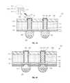
- FIGS. 1A and 1Bcross-sectional views of a semiconductor device according to various embodiments are illustrated.
- a semiconductor device 101includes a semiconductor die 110 , a through electrode 120 , a dielectric layer 130 , a conductive pad 140 , and a conductive bump 150 .
- the semiconductor die 110includes a substantially planar first surface 111 , a substantially planar second surface 112 opposing the first surface 111 . Also, the semiconductor die 110 further includes a through hole 113 penetrating the first surface 111 and the second surface 112 . Also, the semiconductor die 110 further includes an insulating layer 114 on the inner wall of the through hole 113 .
- the semiconductor die 110includes an active region 115 disposed on the second surface 112 , a bond pad 116 formed on the active region 115 , and another insulating layer 117 covering the circumference of the bond pad 116 and the active region 115 .
- the first surface 111is sometimes called the inactive surface of the semiconductor die 110 whereas the second surface 112 is sometimes called the active surface of the semiconductor die 110 .
- the insulating layer 114serves to prevent the through electrode 120 from being electrically shorted to the semiconductor die 110 , and the outer insulating layer 117 provides appropriate protection for the active region 115 from external foreign substances.
- Those insulating layers 114 and 117may be formed of any one selected from the group consisting of silicon oxide, silicon nitride, polymer and equivalents thereof. However, in other embodiments, the kinds of insulating layers 114 and 117 are not limited.
- the through electrode 120is provided inside the through hole 113 , that is, inside the insulating layer 114 .
- the through electrode 120is substantially formed in the through hole 113 , and extends and protrudes upwardly to a predetermined length through and above the first surface 111 .
- the through electrode 120 extending through and protruding above the first surface 111includes a top surface 121 and both side surfaces 122 , and the top surface 121 is substantially planar.
- the exposed side surfaces 122are sometimes called an exposed sidewall 122 of the through electrode 120 , i.e., the portion of the sidewall of the through electrode 120 exposed from the dielectric layer 130 .
- the through electrode 120may be formed of any one of copper, tungsten, aluminum, gold, silver, and equivalents thereof in general, but the materials of the through electrode 120 is not limited thereto. Furthermore, the through electrode 120 may further include a barrier or seed layer (not shown) disposed on the inner wall of the insulating layer 114 .
- the dielectric layer 130is disposed on the first surface 111 of the semiconductor die 110 and has a predetermined thickness. Also, the dielectric layer 130 may have an opening 131 in a region corresponding to the through electrode 120 . This opening 131 may have an inclined sectional shape. That is, the opening 131 may have a relatively small lower region and a relatively wide upper region.
- the through electrode 120penetrates the opening 131 , and extends and protrudes upwardly to a predetermined length.
- the length (or thickness) of the through electrode 120 extending and protruding upwardly from the first surface 111 of the semiconductor die 110may be smaller than, equal to, or greater than the maximum thickness of the dielectric layer 130 .
- the maximum thickness of the dielectric layer 130may be greater than, equal to, or smaller than the length (or thickness) of the through electrode 120 extending and protruding upwardly from the first surface 111 of the semiconductor die 110 .
- the opening 131is formed in part of the dielectric layer 130 , the first surface 111 of the semiconductor die 110 is not exposed through the opening 131 . That is, the opening 131 does not fully penetrate the dielectric layer 130 but is formed in part of the dielectric layer 130 .
- the dielectric layer 130may be formed of at least one selected from the group consisting of Poly Benz Oxazole (PBO), PolyImide (PI), Benzo Cyclo Butene (BCB), BismaleimideTriazine (BT), phenolic resin, epoxy, Silicone, Si3N4, SiO2, and equivalents thereof, but the material of the dielectric layer 130 is not limited thereto. Also, even though a single dielectric layer 130 is illustrated in the drawing, multiple dielectric layers 130 may be used.
- the conductive pad 140includes a first electroless plating layer 141 , a second electroless plating layer 142 , and a third electroless plating layer 143 .
- the first electroless plating layer 141roughly surrounds the through electrode 120 inside the opening 131 . That is, the first electroless plating layer 141 surrounds the top surface 121 and both side surfaces 122 of the through electrode 120 exposed within the opening 131 .
- the second electroless plating layer 142surrounds the first electroless plating layer 141 .
- the third electroless plating layer 143surrounds the second electroless plating layer 142 .
- the lower ends of the first, second and third electroless plating layers 141 , 142 and 143may or may not contact the surface of the opening 131 .
- the first electroless plating layer 141may be formed of nickel or equivalents thereof in general, but the material of the first electroless plating layer 141 is not limited thereto.
- the second electroless plating layer 142may be palladium or equivalents thereof, but the material of the second electroless plating layer 142 is not limited thereto.
- the third electroless plating layer 143may be formed of gold or equivalents thereof, but the material of the third electroless plating layer 143 is not limited thereto.
- the third electroless plating layer 143suppresses the oxidation of the through electrode 120 . Also, the first electroless plating layer 141 and the second electroless plating layer 142 suppress interaction between the through electrode 120 and the third electroless plating layer 143 .
- the second electroless plating layer 142may not be formed in some cases.
- such a conductive pad 140protrudes upwardly with a predetermined thickness or is exposed through the surface of the dielectric layer 130 .
- the conductive pad 140serves to facilitate the stacking of a plurality of semiconductor devices 101 .
- the conductive bump 150is formed on the bond pad 116 , and extends downwardly from the second surface 112 .
- the through electrode 120 , the active region 115 , and the bond pad 116may be electrically connected.
- the conductive bump 150has a diameter greater than the diameter of the through electrode 120 , thus allowing the conductive bump 150 to be stably mounted on an external device. Furthermore, the conductive bump 150 may come into contact with the insulating layer 117 by having a relatively great diameter. That is, the insulating layer 117 may be interposed between the bond pad 116 and the conductive bump 150 .
- the conductive bump 150may be formed of the same material as the through electrode 120 . Additionally, the conductive bump 150 may be formed of a material such as solder (SnPb, SnAg) or the like. Furthermore, in one embodiment, a solder cap 151 is formed on the conductive bump 150 , however, the solder cap 151 is not an essential element. Of course, in a case where there is a solder cap 151 , the semiconductor device 101 can be more easily mounted on an external device.
- the semiconductor device 101has the conductive pad 140 formed by an electroless plating method, and thus seed metal is not required, and there is no need for a high-temperature sputtering process for the formation of seed metal.
- a semiconductor device 102includes another insulating layer 118 on the surface of the insulating layer 117 .
- the insulating layer 118also covers a predetermined region of the bond pad 116 .
- a predetermined region of the conductive bump 150also contacts the insulating layer 118 .
- the insulating layers 117 and 118may be interposed between the bond pad 116 and the conductive bump 150 .
- the insulating layer 118may be substantially formed of any one selected from the group consisting of Poly Benz Oxazole (PBO), PolyImide (PI), Benzo Cyclo Butene (BCB), BismaleimideTriazine (BT), phenolic resin, epoxy, Silicone, Si3N4, SiO2, and equivalents thereof, but the material of the insulating layer 118 is not limited thereto.
- PBOPoly Benz Oxazole
- PIPolyImide
- BCBBenzo Cyclo Butene
- BTBismaleimideTriazine
- phenolic resinepoxy, Silicone, Si3N4, SiO2, and equivalents thereof, but the material of the insulating layer 118 is not limited thereto.
- the insulating layer 118can efficiently absorb stress acting on the conductive bump 150 .
- cracking between the bond pad 116 and the conductive bump 150is efficiently prevented.
- the insulating layer 118is not described in the following embodiments, those of skill in the art will understand that the insulating layer 118 is applied to each embodiment in other examples.
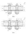
- FIG. 2a cross-sectional view of a semiconductor device 201 according to another embodiment is illustrated.
- the semiconductor device 201 according to another embodimentis similar to the semiconductor device 101 shown in FIG. 1A , and thus only the significant differences will be described.
- a dielectric layer 230does not having an opening, and instead, may have a slightly protruding projection 231 . That is, the through electrode 120 extends and protrudes upwardly to a predetermined length through the slight projection 231 rather than an opening. Accordingly, the thickness (or length) of the through electrode 120 substantially extending from the first surface 111 of the semiconductor die 110 may be slightly greater than the thickness of the dielectric layer 230 .
- a conductive pad 240is formed by an electroless plating method on the through electrode 120 extending and protruding upwardly to a predetermined length through the projection 231 of the dielectric layer 230 . That is, the conductive pad 240 includes a first electroless plating layer surrounding the top surface 121 and both side surfaces 122 of the through electrode 120 and disposed on the surface of the dielectric layer 230 , a second electroless plating layer covering the first electroless plating layer, and a third electroless plating layer covering the second electroless plating layer.
- the top surface of the conductive pad 240has a substantially planar shape.
- the conductive pad 240may or may not come into contact with the projection 231 of the dielectric layer 230 .
- the first, second and third electroless plating layersare similar to the layers 141 , 142 , 143 as discussed above in reference to semiconductor device 101 , and thus a detailed description thereof is omitted.
- the semiconductor device 201is manufactured by exposing the through electrode 120 by applying a blanket process to the dielectric layer 230 , and then applying a plating process to the top surface 121 and both side surfaces 122 of the exposed through electrode 120 .
- the blanket processrenders the dielectric layer 230 the thickest in a region (the projection 231 ) corresponding to the through electrode 120 , and gradually thinner as it is distanced from the through electrode 120 .
- the blanket processmeans wet or dry etching performed upon the entire top surface of the dielectric layer 230 .
- FIG. 3a cross-sectional view of a semiconductor device 301 according to another embodiment is illustrated.
- the semiconductor device 301 according to another embodimentis similar to the semiconductor device 201 illustrated in FIG. 2 , and thus only the significant differences will now be described.
- a dielectric layer 330does not have an opening or a protrusion. That is, the top surface 332 of the dielectric layer 330 may be in the same plane as the top surface 121 of the through electrode 120 . Furthermore, a conductive pad 340 is formed on only the top surface 121 of the through electrode 120 . That is, the conductive pad 340 is not formed on the sidewall of the through electrode 120 , and thus the conductive pad 340 has a substantially planar shape. Here, the top surface 121 of the through electrode 120 has a substantially planar shape.
- the semiconductor device 301is manufactured by exposing the through electrode 120 through a chemical mechanical polishing (CMP) to the dielectric layer 330 , and applying a plating process to the top surface 121 of the exposed through electrode 120 .
- CMPchemical mechanical polishing
- the top surface 121 of the through electrode 120 and the top surface 332 of the dielectric layer 330are all in the same plane.
- the manufacturing method of the semiconductor device 101 according to another embodimentincludes forming a through electrode, etching a semiconductor die, forming a dielectric layer, forming an opening, and forming a conductive pad.
- a through hole 113is formed in a semiconductor die 110 having a first surface 111 A and a second surface 112 opposing the first surface 111 A, and an insulating layer 114 is formed on the inner wall of the through hole 113 . Thereafter, a through electrode 120 is formed inside the insulating layer 114 .
- the through hole 113is formed by any one of laser drilling, wet etching, dry etching, or equivalent methods thereof, but the method for forming the through hole 113 is not limited thereto.
- the laser drillingunlike wet etching or dry etching, does not require a mask manufacturing process, a photo-process or the like, and allows the length and width of the through hole 113 to be set relatively easily.
- the insulating layer 114may be formed of silicon oxide (SiOx) or silicon nitride (SiNx) by using a chemical vapor deposition (CVD) method or may be formed of a polymer by using a spin coating method or a sublimation method.
- the method for forming the insulating layer 114is not limited to the described ones.
- the through electrode 120may be formed of any one selected from the group consisting of copper, tungsten, aluminum, gold, silver or equivalents thereof, but the material of the through electrode 120 is not limited thereto.
- a barrier and/or seed layermay be formed on the inner wall of the through hole 113 (i.e., the inner wall of the insulating layer 114 ). Furthermore, the through electrode 120 may be formed of an electroplating process or an electroless plating process.
- a conductive bump 150is formed on the bond pad 116 .
- the conductive bump 150has a greater diameter than that the through electrode 120 .
- a solder cap 151may be formed on the conductive bump 150 .
- the top surface 121 of the through electrode 120may be formed to be in the same plane as the first surface 111 A of the semiconductor die 110 .
- the first surface 111 A of the semiconductor die 110may be formed through back-grinding such that the top surface 121 of the through electrode 120 is exposed externally through the first surface 111 A of the semiconductor die 110 .
- the top surface 121 of the through electrode 120is substantially planar. Furthermore, a region removed by the back-grinding is an inactive region other than an active region 115 , and the removal thereof does not have any influence on the operation of the semiconductor die 110 .
- Reference numeral 117 in the drawingindicates another insulating layer covering the active region 115 and the circumference of the bond pad 116 .
- the first surface 111 A ( FIG. 4A ) of the semiconductor die 110is removed to a predetermined depth by dry etching or wet etching to form the first surface 111 ( FIG. 4B ).
- an etchant used in the dry etching or the wet etchingaffects only the semiconductor die 110 and the insulating layer 114 , and has no influence on the through electrode 120 . Accordingly, this etching provides a portion of the through electrode 120 extending and protruding upwardly to a predetermined length through the semiconductor die 110 and the insulating layer 114 .
- the first surface 111 of the semiconductor die 110is coated with a dielectric layer 130 with a sufficient thickness to cover the through electrode 120 .
- the dielectric layer 130is formed by, for example, a spin coating method, but the coating method of the dielectric layer 130 is not limited.
- the dielectric layer 130may be formed of one selected from the group consisting of Poly Benz Oxazole (PBO), PolyImide (PI), Benzo Cyclo Butene (BCB), BismaleimideTriazine (BT), phenolic resin, epoxy, Silicone, and equivalents thereof, but the material of the dielectric layer 130 is not limited thereto.
- the thickness of the dielectric layer 130becomes greater than the length (or thickness) of the through electrode 120 extending and protruding from the first surface 111 of the semiconductor die 110 .
- the dielectric layer 130is removed partially corresponding to the through electrode 120 , thus forming an opening 131 with a predetermined depth and width.
- a maskis formed on a portion of the dielectric layer 130 not corresponding to the through electrode 120 , and is not formed on the other portion of the dielectric layer 130 which does corresponding to the through electrode 120 .
- the opening 131with a predetermined depth and width is formed.
- the opening 131has an inclined shape. That is, the opening 131 has a narrower lower region and is widened toward its upper region.
- the through electrode 120i.e., the exposed top surface 121 and both side surfaces 122 , is exposed to the outside through the opening 131 .
- a conductive pad 140is formed on the through electrode 120 , extending and protruding through the opening 131 , by an electroless plating method.
- the conductive pad 140includes a first electroless plating layer 141 , a second electroplating layer 142 , and a third electroplating layer 143 as described above.
- the first electroless plating layer 141is formed to surround the through electrode 120 . Furthermore, the second electroless plating layer 142 roughly covers the first electroless plating layer 141 . Also, the third electroless plating layer 143 roughly covers the second electroless plating layer 142 .
- the first electroless plating layer 141may be formed of nickel or equivalents thereof.
- the second electroless plating layer 142may be formed of palladium or equivalents thereof.
- the third electroless plating layer 143may be formed of gold or equivalents thereof.
- the second electroless plating layer 142may not be formed in some cases.
- the conductive pad 140is formed by an electroless plating method as described above, there is no need for seed metal, as well as a high-temperature sputtering process for the formation of seed metal.
- the entirety of the top surface of the dielectric layer 130is dry- or wet-etched by using the blanket process to form the dielectric layer 230 ( FIG. 2 ), thus causing the through electrode 120 to protrude, and subsequently the conductive pad 240 is formed on the through electrode 120 .
- the semiconductor device 201 shown in FIG. 2is obtained through wet or dry etching.
- the entirety of the top surface of the dielectric layer 130is subjected to grinding by using a CMP process to form the dielectric layer 330 ( FIG. 3 ), thus exposing the through electrode 120 , and subsequently, the conductive pad 340 is formed on the through electrode 120 .
- the semiconductor device 301 shown in FIG. 3is obtained.
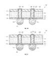
- FIG. 5a cross-sectional view of a semiconductor device 401 according to another embodiment is illustrated.
- the semiconductor device 401 according to another embodimentis similar to the semiconductor device 101 shown in FIG. 1A , and thus only the significant differences will now be described.
- An insulating layer 414 surrounding the through electrode 120may extend not only between the first surface 111 and the second surface 112 of the semiconductor die 110 as in FIG. 1A but also to an opening 431 in a dielectric layer 430 . That is, the insulating layer 414 extends upwardly to a predetermined length through the first surface 111 of the semiconductor die 110 , and thus is interposed between the dielectric layer 430 and the through electrode 120 . In the above manner, the dielectric layer 430 contacts the insulating layer 414 , rather than the through electrode 120 .
- a conductive pad 440may be disposed on the through electrode 120 outside the insulating layer 414 . That is, the conductive pad 440 is formed on the top surface 121 and both side surfaces 122 of the through electrode 120 protruding through the insulating layer 414 , and the thickness of the conductive pad 440 may be almost similar to the thickness of the insulating layer 414 , but the thickness of the conductive pad 440 is not limited thereto.
- the top surface 121 of the through electrode 120is not planar but substantially curved.
- the through electrode 120does not come into direct contact with the dielectric layer 430 . That is, the insulating layer 414 is further interposed between the through electrode 120 and the dielectric layer 430 . Accordingly, insulating properties for the through electrode 120 are more enhanced.
- FIG. 6a cross-sectional view of a semiconductor device 501 according to another embodiment is illustrated.
- the semiconductor device 501 according to this embodimentis similar to the semiconductor device 201 shown in FIG. 2 , and thus only the significant differences will now be described.
- An insulating layer 514fully covers both side portions, i.e., the entire sidewall, of the through electrode 120 . That is, the insulating layer 514 is formed not only between the first surface 111 and the second surface 112 of the semiconductor die 110 but also between the through electrode 120 and a dielectric layer 530 . In other words, the entirety of the outer cylindrical sidewall other than the top surface 121 of the through electrode 120 is covered with the insulating layer 514 . Accordingly, the through electrode 120 and the dielectric layer 530 do not come into direct contact with each other. Also, the dielectric layer 530 formed around the insulating layer 514 may further include a projection 531 in a region corresponding to the through electrode 120 .
- a conductive pad 540is formed on only the top surface 121 of the through electrode 120 exposed through the insulating layer 514 .
- the conductive pad 540includes a first electroless plating layer, a second electroless plating layer, and a third electroless plating layer similar to the layers 141 , 142 , 143 described above.
- the top surface 121 of the through electrode 120is not planar but substantially curved.
- the semiconductor device 501is manufactured by applying a blanket process to the dielectric layer 530 to thus expose the through electrode 120 , and applying a plating process to the top surface 121 of the exposed through electrode 120 .
- the dielectric layer 530is the thickest in a region (the protrusion 531 ) corresponding to the through electrode 120 , and becomes thinner as it is distanced from the through electrode 120 .
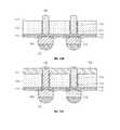
- FIG. 7a cross-sectional view of a semiconductor device 601 according to another embodiment is illustrated.
- the semiconductor device 601 according to another embodimentis similar to the semiconductor device 201 shown in FIG. 2 , and thus only the significant differences will now be described.
- An insulating layer 614fully covers the entire sidewall of the through electrode 120 . Also, the respective top surfaces of the through electrode 120 , the insulating layer 614 and a dielectric layer 630 are in the same plane. Thus, the through electrode 120 and the dielectric 630 do not come into directly contact with each other. Also, a conductive pad 640 is formed on only the top surface 121 of the through electrode 120 exposed through the insulating layer 614 .
- the semiconductor device 601is manufactured by applying a CMP process to the dielectric layer 630 to thus expose the through electrode 120 , and applying a plating process to the top surface 121 of the exposed through electrode 120 .
- the CMP processdue to the CMP process, the respective top surfaces 121 of the through electrode 120 , the insulating layer 614 and the dielectric layer 630 are in the same plane. That is, the top surface 121 of the through electrode 120 has a substantially planar shape.
- the dielectric layer 630does not have any opening or protrusion.
- the method of manufacturing the semiconductor device 401 of FIG. 5includes forming a through electrode, etching a semiconductor die, forming a dielectric layer, forming an opening, and forming a conductive pad.
- a through hole 113is formed in a semiconductor die 110 having a first surface 111 A and a second surface 112 opposing the first surface 111 A, an insulating layer 414 is formed on the inner wall of the through hole 113 , and a through electrode 120 is then formed inside the insulating layer 414 .
- the insulating layer 414surrounds the top surface 121 and the entire sidewall of the through electrode 120 .
- the first surface 111 A of the semiconductor die 110( FIG. 8A ) is removed to a predetermined depth by wet etching or dry etching to form a first surface 111 ( FIG. 8B ).
- an etchant used for the dry etching or the wet etchingaffects only the semiconductor die 110 and does not affect the insulating layer 414 .
- the upper regions of the through electrode 120 and the insulating layer 414extend and protrude upwardly to a predetermined length through the first surface 111 of the semiconductor die 110 .
- the first surface 111 of the semiconductor die 110is coated with a dielectric layer 430 having a sufficient thickness to cover the insulating layer 414 formed on the surface of the through electrode 120 .
- a portion of the dielectric layer 430 corresponding to the through electrode 120is removed to thus form an opening 431 having a predetermined depth and width.
- the insulating layer 414 formed on the through electrode 120is also removed. That is, the insulating layer 414 formed in a region corresponding to the through electrode 120 exposed through the opening 431 is also removed. Accordingly, the through electrode 120 without the insulating layer 414 is exposed to the outside through the opening 431 . However, even in this state, the dielectric layer 430 is in contact with the insulating layer 414 without contacting the through electrode 120 .
- a conductive pad 440is formed on the through electrode 120 extending and protruding through the opening 431 by an electroless plating method.
- a first electroless plating layer, a second electroless plating layer, and a third electroless plating layer as described aboveare sequentially formed to thus form the conductive pad 440 .
- the conductive pad 440can come into contact with the insulating layer 414 and/or the dielectric layer 430 .
- the entirety of the top surface of the dielectric layer 430 and a portion of the insulating layer 414are wet- or dry-etched by using a blanket process to form the dielectric layer 530 ( FIG. 6 ) to thus cause the through electrode 120 to protrude, and subsequently, the conductive pad 540 is formed on the through electrode 120 .
- the semiconductor device 501 shown in FIG. 6is obtained.
- the entirety of the top surface of the dielectric layer 430 and a portion of the insulating layer 414are subjected to grinding by using a CMP process to form the dielectric layer 630 ( FIG. 7 ) to thus expose the through electrode 120 , and subsequently, the conductive pad 640 is formed on the through electrode 120 .
- the semiconductor device 601 shown in FIG. 7is obtained.
- FIG. 9a cross-sectional view of a semiconductor device 701 according to another embodiment is illustrated. As shown in FIG. 9 , the semiconductor device 701 according to another embodiment is similar to the semiconductor device 101 shown in FIG. 1A , and only the significant differences will now be described.
- a conductive pad 740is formed on the through electrode 120 protruding and extending through an opening 731 of a dielectric layer 730 , and the conductive pad 740 contacts an insulating layer 714 surrounding the through electrode 120 . Accordingly, substantially, the dielectric layer 730 does not come into contact with the through electrode 120 , and contacts only the insulating layer 714 and the conductive pad 740 .
- the top surface 121 of the through electrode 120is roughly curved shape, which is not planar.
- FIG. 10a cross-sectional view of a semiconductor device 801 according to another embodiment is illustrated.
- the semiconductor device 801 according to another embodimentis similar to the semiconductor device 201 shown in FIG. 2 , and thus only the significant differences will now be described.
- the top surface 121 of the through electrode 120is exposed through a dielectric layer 830 . That is, the top surface 121 of the through electrode 120 is exposed through a protrusion 831 of the dielectric layer 830 . Also, a conductive pad 840 is formed on the top surface 121 of the exposed through electrode 120 . Accordingly, the conductive pad 840 slightly protrudes through the dielectric layer 830 .
- the top surface 121 of the through electrode 120is not planar and has a substantially curved shape.
- the manufacturing method of the semiconductor device 701 according to another embodimentincludes forming a through electrode, etching a semiconductor die, forming a dielectric layer, forming an opening, and forming a conductive pad.
- a through hole 113is formed in a semiconductor die 110 having a first surface 111 A and a second surface 112 opposing the first surface 111 A, an insulating layer 714 is formed on the inner wall of the through hole 113 , and a through electrode 120 is then formed inside the insulating layer 714 .
- the insulating layer 714surrounds the top surface 121 and the entire sidewall of the through electrode 120 .
- the first surface 111 A of the semiconductor die 110( FIG. 11A ) is removed to a predetermined depth through wet etching or dry etching to form the first surface 111 as illustrated in FIG. 11B .
- An etchant used in the dry etching or the wet etchingaffects only the semiconductor die 110 and the insulating layer 714 , and does not affect the through electrode 120 . Accordingly, due to this etching process, the upper region of the through electrode 120 extends and protrudes upwardly to a predetermined length through the first surface 111 of the semiconductor die 110 .
- the first surface 111 of the semiconductor die 110is coated with a dielectric layer 730 having a sufficient thickness to cover the through electrode 120 .
- a portion of the dielectric layer 730 corresponding to the through electrode 120is removed to thus form an opening 731 extending entirely thorough the dielectric layer 730 to expose the insulating layer 714 .
- the through electrode 120is exposed as well.
- a conductive pad 740is formed on the through electrode 120 extending and protruding through the opening 731 by using an electroless plating method.
- the conductive pad 740extends entirely through the dielectric layer 730 to contact the insulating layer 714 . Accordingly, substantially, the dielectric layer 730 does not come into contact with the through electrode 120 , and contacts only the insulating layer 714 and the conductive pad 740 .
- FIGS. 11 D 2 , 11 E 2are cross-sectional views of the semiconductor device of FIG. 11C at later stages during fabrication in accordance with an alternative embodiment.
- a portion of the dielectric layer 730 corresponding to the through electrode 120is removed to thus form an opening 731 .
- the opening 731extends only partially, but not entirely, through the dielectric layer 730 such that a portion of the dielectric layer 730 remains above the insulating layer 714 .
- the through electrode 120is exposed as well.
- a conductive pad 740is formed on the through electrode 120 extending and protruding through the opening 731 by using an electroless plating method.
- the conductive pad 740extends partially, but not entirely, through the dielectric layer 730 to be space apart from the insulating layer 714 . Accordingly, substantially, a portion of the dielectric layer 730 does come into contact with the through electrode 120 between the insulating layer 714 and the conductive pad 740 .
- the entirety of the top surface of the dielectric layer 730is wet- or dry-etched by using a blanket process to form the dielectric layer 830 ( FIG. 10 ) to thus allow the through electrode 120 to protrude, and subsequently, the conductive pad 840 is formed on the through electrode 120 . In this manner, the semiconductor device 801 shown in FIG. 10 is obtained.
- the entirety of the top surface of the dielectric layer 730is subjected to grinding to form the dielectric layer 330 as illustrated in FIG. 3 to thus expose the through electrode 120 , and subsequently, the conductive pad 340 is formed on the through electrode 120 . In this manner, the semiconductor device 301 shown in FIG. 3 is obtained.
- FIG. 12a state in which the semiconductor device 101 of FIG. 1A is bonded to a carrier wafer 912 by a temporary bonding adhesive 911 for a plating process of a manufacturing method of the semiconductor device 101 according to an embodiment is illustrated.
- the semiconductor device 101is bonded to a carrier wafer 912 by a temporary bonding adhesive 911 . That is, the conductive bump 150 , the solder cap 151 , the insulating layer 117 of the semiconductor device 101 are bonded to the carrier wafer 912 by the temporary bonding adhesive 911 .
- the temporary bonding adhesive 911has a low level of viscosity at a high-temperature process in general, the semiconductor device 101 is easily separated from the carrier wafer 912 in a high-temperature process. Furthermore, a gas generated from the temporary bonding adhesive 911 may cause cracking in the semiconductor device 101 . That is, the temporary bonding adhesive 911 is not suitable for a high-temperature process such as existing sputtering.
- a low-temperature processsuch as plating is used rather than a high-temperature process such as sputtering, and thus the semiconductor device 101 is not easily separated from the carrier wafer 912 during a plating process. Also, the use of the low-temperature process does not cause gas generation from the temporary bonding adhesive 911 , and prevents cracking in the semiconductor device 101 .
Landscapes
- Engineering & Computer Science (AREA)
- Computer Hardware Design (AREA)
- Microelectronics & Electronic Packaging (AREA)
- Power Engineering (AREA)
- Manufacturing & Machinery (AREA)
- Physics & Mathematics (AREA)
- Condensed Matter Physics & Semiconductors (AREA)
- General Physics & Mathematics (AREA)
- Internal Circuitry In Semiconductor Integrated Circuit Devices (AREA)
Abstract
Description
Claims (17)
Priority Applications (6)
| Application Number | Priority Date | Filing Date | Title |
|---|---|---|---|
| US13/306,685US8552548B1 (en) | 2011-11-29 | 2011-11-29 | Conductive pad on protruding through electrode semiconductor device |
| US14/017,797US8981572B1 (en) | 2011-11-29 | 2013-09-04 | Conductive pad on protruding through electrode semiconductor device |
| US14/615,127US9431323B1 (en) | 2011-11-29 | 2015-02-05 | Conductive pad on protruding through electrode |
| US15/250,397US9947623B1 (en) | 2011-11-29 | 2016-08-29 | Semiconductor device comprising a conductive pad on a protruding-through electrode |
| US15/953,024US10410967B1 (en) | 2011-11-29 | 2018-04-13 | Electronic device comprising a conductive pad on a protruding-through electrode |
| US16/564,333US11043458B2 (en) | 2011-11-29 | 2019-09-09 | Method of manufacturing an electronic device comprising a conductive pad on a protruding-through electrode |
Applications Claiming Priority (1)
| Application Number | Priority Date | Filing Date | Title |
|---|---|---|---|
| US13/306,685US8552548B1 (en) | 2011-11-29 | 2011-11-29 | Conductive pad on protruding through electrode semiconductor device |
Related Child Applications (1)
| Application Number | Title | Priority Date | Filing Date |
|---|---|---|---|
| US14/017,797ContinuationUS8981572B1 (en) | 2011-11-29 | 2013-09-04 | Conductive pad on protruding through electrode semiconductor device |
Publications (1)
| Publication Number | Publication Date |
|---|---|
| US8552548B1true US8552548B1 (en) | 2013-10-08 |
Family
ID=49262475
Family Applications (6)
| Application Number | Title | Priority Date | Filing Date |
|---|---|---|---|
| US13/306,685Active2031-12-05US8552548B1 (en) | 2011-11-29 | 2011-11-29 | Conductive pad on protruding through electrode semiconductor device |
| US14/017,797ActiveUS8981572B1 (en) | 2011-11-29 | 2013-09-04 | Conductive pad on protruding through electrode semiconductor device |
| US14/615,127ActiveUS9431323B1 (en) | 2011-11-29 | 2015-02-05 | Conductive pad on protruding through electrode |
| US15/250,397ActiveUS9947623B1 (en) | 2011-11-29 | 2016-08-29 | Semiconductor device comprising a conductive pad on a protruding-through electrode |
| US15/953,024ActiveUS10410967B1 (en) | 2011-11-29 | 2018-04-13 | Electronic device comprising a conductive pad on a protruding-through electrode |
| US16/564,333ActiveUS11043458B2 (en) | 2011-11-29 | 2019-09-09 | Method of manufacturing an electronic device comprising a conductive pad on a protruding-through electrode |
Family Applications After (5)
| Application Number | Title | Priority Date | Filing Date |
|---|---|---|---|
| US14/017,797ActiveUS8981572B1 (en) | 2011-11-29 | 2013-09-04 | Conductive pad on protruding through electrode semiconductor device |
| US14/615,127ActiveUS9431323B1 (en) | 2011-11-29 | 2015-02-05 | Conductive pad on protruding through electrode |
| US15/250,397ActiveUS9947623B1 (en) | 2011-11-29 | 2016-08-29 | Semiconductor device comprising a conductive pad on a protruding-through electrode |
| US15/953,024ActiveUS10410967B1 (en) | 2011-11-29 | 2018-04-13 | Electronic device comprising a conductive pad on a protruding-through electrode |
| US16/564,333ActiveUS11043458B2 (en) | 2011-11-29 | 2019-09-09 | Method of manufacturing an electronic device comprising a conductive pad on a protruding-through electrode |
Country Status (1)
| Country | Link |
|---|---|
| US (6) | US8552548B1 (en) |
Cited By (15)
| Publication number | Priority date | Publication date | Assignee | Title |
|---|---|---|---|---|
| US20140103527A1 (en)* | 2012-03-23 | 2014-04-17 | Stats Chippac, Ltd. | Semiconductor Device and Method of Forming a POP Device with Embedded Vertical Interconnect Units |
| US20140346645A1 (en)* | 2013-05-23 | 2014-11-27 | United Microelectronics Corp. | Through silicon via and process thereof |
| US20150263647A1 (en)* | 2014-03-15 | 2015-09-17 | Canon Kabushiki Kaisha | Device having element electrode connected to penetrating wire, and method for manufacturing the same |
| CN104934392A (en)* | 2014-03-19 | 2015-09-23 | 爱思开海力士有限公司 | Semiconductor Devices Having Through Electrodes And Methods Of Manufacturing The Same |
| CN104952831A (en)* | 2014-03-28 | 2015-09-30 | 爱思开海力士有限公司 | Semiconductor devices having through electrodes, methods of manufacturing the same, and semiconductor packages including the same |
| WO2016039223A1 (en)* | 2014-09-09 | 2016-03-17 | 大日本印刷株式会社 | Structural body and method for manufacturing same |
| US9431323B1 (en) | 2011-11-29 | 2016-08-30 | Amkor Technology, Inc. | Conductive pad on protruding through electrode |
| US20160300790A1 (en)* | 2015-04-07 | 2016-10-13 | Hyesun YOON | Package substrates and methods of fabricating the same |
| WO2016176692A3 (en)* | 2016-06-17 | 2017-01-05 | Ohmx Corporation | Biosensor chip |
| US9837303B2 (en) | 2012-03-23 | 2017-12-05 | STATS ChipPAC Pte. Ltd. | Semiconductor method and device of forming a fan-out device with PWB vertical interconnect units |
| US9865525B2 (en) | 2012-03-23 | 2018-01-09 | STATS ChipPAC Pte. Ltd. | Semiconductor method and device of forming a fan-out PoP device with PWB vertical interconnect units |
| US10049964B2 (en) | 2012-03-23 | 2018-08-14 | STATS ChipPAC Pte. Ltd. | Semiconductor device and method of forming a fan-out PoP device with PWB vertical interconnect units |
| US11177331B2 (en)* | 2018-10-30 | 2021-11-16 | Samsung Display Co., Ltd. | Semiconductor device and display device having the same |
| US11515254B2 (en)* | 2020-07-15 | 2022-11-29 | SK Hynix Inc. | Semiconductor chip including penetrating electrodes, and semiconductor package including the semiconductor chip |
| US20230082878A1 (en)* | 2021-09-14 | 2023-03-16 | United Microelectronics Corp. | Semiconductor structure |
Families Citing this family (1)
| Publication number | Priority date | Publication date | Assignee | Title |
|---|---|---|---|---|
| KR20190067839A (en) | 2016-10-04 | 2019-06-17 | 스카이워크스 솔루션즈, 인코포레이티드 | Two-sided radio-frequency package with overmolded structure |
Citations (401)
| Publication number | Priority date | Publication date | Assignee | Title |
|---|---|---|---|---|
| US2596993A (en) | 1949-01-13 | 1952-05-20 | United Shoe Machinery Corp | Method and mold for covering of eyelets by plastic injection |
| US3435815A (en) | 1966-07-15 | 1969-04-01 | Micro Tech Mfg Inc | Wafer dicer |
| US3734660A (en) | 1970-01-09 | 1973-05-22 | Tuthill Pump Co | Apparatus for fabricating a bearing device |
| US3838984A (en) | 1973-04-16 | 1974-10-01 | Sperry Rand Corp | Flexible carrier and interconnect for uncased ic chips |
| US4054238A (en) | 1976-03-23 | 1977-10-18 | Western Electric Company, Inc. | Method, apparatus and lead frame for assembling leads with terminals on a substrate |
| US4189342A (en) | 1971-10-07 | 1980-02-19 | U.S. Philips Corporation | Semiconductor device comprising projecting contact layers |
| US4258381A (en) | 1977-12-07 | 1981-03-24 | Steag, Kernergie Gmbh | Lead frame for a semiconductor device suitable for mass production |
| US4289922A (en) | 1979-09-04 | 1981-09-15 | Plessey Incorporated | Integrated circuit package and lead frame |
| US4301464A (en) | 1978-08-02 | 1981-11-17 | Hitachi, Ltd. | Lead frame and semiconductor device employing the same with improved arrangement of supporting leads for securing the semiconductor supporting member |
| US4332537A (en) | 1978-07-17 | 1982-06-01 | Dusan Slepcevic | Encapsulation mold with removable cavity plates |
| US4394712A (en) | 1981-03-18 | 1983-07-19 | General Electric Company | Alignment-enhancing feed-through conductors for stackable silicon-on-sapphire wafers |
| US4417266A (en) | 1981-08-14 | 1983-11-22 | Amp Incorporated | Power and ground plane structure for chip carrier |
| US4451224A (en) | 1982-03-25 | 1984-05-29 | General Electric Company | Mold device for making plastic articles from resin |
| US4499655A (en) | 1981-03-18 | 1985-02-19 | General Electric Company | Method for making alignment-enhancing feed-through conductors for stackable silicon-on-sapphire |
| US4530152A (en) | 1982-04-01 | 1985-07-23 | Compagnie Industrielle Des Telecommunications Cit-Alcatel | Method for encapsulating semiconductor components using temporary substrates |
| US4541003A (en) | 1978-12-27 | 1985-09-10 | Hitachi, Ltd. | Semiconductor device including an alpha-particle shield |
| US4646710A (en) | 1982-09-22 | 1987-03-03 | Crystal Systems, Inc. | Multi-wafer slicing with a fixed abrasive |
| US4707724A (en) | 1984-06-04 | 1987-11-17 | Hitachi, Ltd. | Semiconductor device and method of manufacturing thereof |
| US4727633A (en) | 1985-08-08 | 1988-03-01 | Tektronix, Inc. | Method of securing metallic members together |
| US4729061A (en) | 1985-04-29 | 1988-03-01 | Advanced Micro Devices, Inc. | Chip on board package for integrated circuit devices using printed circuit boards and means for conveying the heat to the opposite side of the package from the chip mounting side to permit the heat to dissipate therefrom |
| US4737839A (en) | 1984-03-19 | 1988-04-12 | Trilogy Computer Development Partners, Ltd. | Semiconductor chip mounting system |
| US4756080A (en) | 1986-01-27 | 1988-07-12 | American Microsystems, Inc. | Metal foil semiconductor interconnection method |
| US4812896A (en) | 1986-11-13 | 1989-03-14 | Olin Corporation | Metal electronic package sealed with thermoplastic having a grafted metal deactivator and antioxidant |
| US4862246A (en) | 1984-09-26 | 1989-08-29 | Hitachi, Ltd. | Semiconductor device lead frame with etched through holes |
| US4862245A (en) | 1985-04-18 | 1989-08-29 | International Business Machines Corporation | Package semiconductor chip |
| US4907067A (en) | 1988-05-11 | 1990-03-06 | Texas Instruments Incorporated | Thermally efficient power device package |
| US4920074A (en) | 1987-02-25 | 1990-04-24 | Hitachi, Ltd. | Surface mount plastic package semiconductor integrated circuit, manufacturing method thereof, as well as mounting method and mounted structure thereof |
| US4935803A (en) | 1988-09-09 | 1990-06-19 | Motorola, Inc. | Self-centering electrode for power devices |
| US4942454A (en) | 1987-08-05 | 1990-07-17 | Mitsubishi Denki Kabushiki Kaisha | Resin sealed semiconductor device |
| US4987475A (en) | 1988-02-29 | 1991-01-22 | Digital Equipment Corporation | Alignment of leads for ceramic integrated circuit packages |
| US5018003A (en) | 1988-10-20 | 1991-05-21 | Mitsubishi Denki Kabushiki Kaisha | Lead frame and semiconductor device |
| US5029386A (en) | 1990-09-17 | 1991-07-09 | Hewlett-Packard Company | Hierarchical tape automated bonding method |
| US5041902A (en) | 1989-12-14 | 1991-08-20 | Motorola, Inc. | Molded electronic package with compression structures |
| US5057900A (en) | 1988-10-17 | 1991-10-15 | Semiconductor Energy Laboratory Co., Ltd. | Electronic device and a manufacturing method for the same |
| US5059379A (en) | 1987-07-20 | 1991-10-22 | Mitsubishi Denki Kabushiki Kaisha | Method of resin sealing semiconductor devices |
| US5065223A (en) | 1989-05-31 | 1991-11-12 | Fujitsu Vlsi Limited | Packaged semiconductor device |
| US5070039A (en) | 1989-04-13 | 1991-12-03 | Texas Instruments Incorporated | Method of making an integrated circuit using a pre-served dam bar to reduce mold flash and to facilitate flash removal |
| US5087961A (en) | 1987-01-28 | 1992-02-11 | Lsi Logic Corporation | Semiconductor device package |
| US5091341A (en) | 1989-05-22 | 1992-02-25 | Kabushiki Kaisha Toshiba | Method of sealing semiconductor device with resin by pressing a lead frame to a heat sink using an upper mold pressure member |
| US5096852A (en) | 1988-06-02 | 1992-03-17 | Burr-Brown Corporation | Method of making plastic encapsulated multichip hybrid integrated circuits |
| US5118298A (en) | 1991-04-04 | 1992-06-02 | Advanced Interconnections Corporation | Through hole mounting of integrated circuit adapter leads |
| US5122860A (en) | 1987-08-26 | 1992-06-16 | Matsushita Electric Industrial Co., Ltd. | Integrated circuit device and manufacturing method thereof |
| US5134773A (en) | 1989-05-26 | 1992-08-04 | Gerard Lemaire | Method for making a credit card containing a microprocessor chip |
| US5151039A (en) | 1990-04-06 | 1992-09-29 | Advanced Interconnections Corporation | Integrated circuit adapter having gullwing-shaped leads |
| US5157480A (en) | 1991-02-06 | 1992-10-20 | Motorola, Inc. | Semiconductor device having dual electrical contact sites |
| US5157475A (en) | 1988-07-08 | 1992-10-20 | Oki Electric Industry Co., Ltd. | Semiconductor device having a particular conductive lead structure |
| US5168368A (en) | 1991-05-09 | 1992-12-01 | International Business Machines Corporation | Lead frame-chip package with improved configuration |
| US5172214A (en) | 1991-02-06 | 1992-12-15 | Motorola, Inc. | Leadless semiconductor device and method for making the same |
| US5172213A (en) | 1991-05-23 | 1992-12-15 | At&T Bell Laboratories | Molded circuit package having heat dissipating post |
| US5175060A (en) | 1989-07-01 | 1992-12-29 | Ibiden Co., Ltd. | Leadframe semiconductor-mounting substrate having a roughened adhesive conductor circuit substrate and method of producing the same |
| US5200362A (en) | 1989-09-06 | 1993-04-06 | Motorola, Inc. | Method of attaching conductive traces to an encapsulated semiconductor die using a removable transfer film |
| US5200809A (en) | 1991-09-27 | 1993-04-06 | Vlsi Technology, Inc. | Exposed die-attach heatsink package |
| US5216278A (en) | 1990-12-04 | 1993-06-01 | Motorola, Inc. | Semiconductor device having a pad array carrier package |
| US5214845A (en) | 1992-05-11 | 1993-06-01 | Micron Technology, Inc. | Method for producing high speed integrated circuits |
| US5218231A (en) | 1989-08-30 | 1993-06-08 | Kabushiki Kaisha Toshiba | Mold-type semiconductor device |
| US5221642A (en) | 1991-08-15 | 1993-06-22 | Staktek Corporation | Lead-on-chip integrated circuit fabrication method |
| US5229647A (en) | 1991-03-27 | 1993-07-20 | Micron Technology, Inc. | High density data storage using stacked wafers |
| US5245751A (en) | 1990-04-27 | 1993-09-21 | Circuit Components, Incorporated | Array connector |
| US5250841A (en) | 1992-04-06 | 1993-10-05 | Motorola, Inc. | Semiconductor device with test-only leads |
| US5252853A (en) | 1991-09-19 | 1993-10-12 | Mitsubishi Denki Kabushiki Kaisha | Packaged semiconductor device having tab tape and particular power distribution lead structure |
| US5258094A (en) | 1991-09-18 | 1993-11-02 | Nec Corporation | Method for producing multilayer printed wiring boards |
| US5266834A (en) | 1989-03-13 | 1993-11-30 | Hitachi Ltd. | Semiconductor device and an electronic device with the semiconductor devices mounted thereon |
| US5268310A (en) | 1992-11-25 | 1993-12-07 | M/A-Com, Inc. | Method for making a mesa type PIN diode |
| US5277972A (en) | 1988-09-29 | 1994-01-11 | Tomoegawa Paper Co., Ltd. | Adhesive tapes |
| US5278446A (en) | 1992-07-06 | 1994-01-11 | Motorola, Inc. | Reduced stress plastic package |
| US5279029A (en) | 1990-08-01 | 1994-01-18 | Staktek Corporation | Ultra high density integrated circuit packages method |
| US5281849A (en) | 1991-05-07 | 1994-01-25 | Singh Deo Narendra N | Semiconductor package with segmented lead frame |
| US5294897A (en) | 1992-07-20 | 1994-03-15 | Mitsubishi Denki Kabushiki Kaisha | Microwave IC package |
| US5327008A (en) | 1993-03-22 | 1994-07-05 | Motorola Inc. | Semiconductor device having universal low-stress die support and method for making the same |
| US5332864A (en) | 1991-12-27 | 1994-07-26 | Vlsi Technology, Inc. | Integrated circuit package having an interposer |
| US5336931A (en) | 1993-09-03 | 1994-08-09 | Motorola, Inc. | Anchoring method for flow formed integrated circuit covers |
| US5335771A (en) | 1990-09-25 | 1994-08-09 | R. H. Murphy Company, Inc. | Spacer trays for stacking storage trays with integrated circuits |
| US5343076A (en) | 1990-07-21 | 1994-08-30 | Mitsui Petrochemical Industries, Ltd. | Semiconductor device with an airtight space formed internally within a hollow package |
| US5353498A (en) | 1993-02-08 | 1994-10-11 | General Electric Company | Method for fabricating an integrated circuit module |
| US5358905A (en) | 1993-04-02 | 1994-10-25 | Texas Instruments Incorporated | Semiconductor device having die pad locking to substantially reduce package cracking |
| US5365106A (en) | 1992-10-27 | 1994-11-15 | Kabushiki Kaisha Toshiba | Resin mold semiconductor device |
| US5381042A (en) | 1992-03-31 | 1995-01-10 | Amkor Electronics, Inc. | Packaged integrated circuit including heat slug having an exposed surface |
| EP0393997B1 (en) | 1989-04-20 | 1995-02-01 | Honeywell Inc. | Method of providing a variable-pitch leadframe assembly |
| US5391439A (en) | 1990-09-27 | 1995-02-21 | Dai Nippon Printing Co., Ltd. | Leadframe adapted to support semiconductor elements |
| US5394303A (en) | 1992-09-11 | 1995-02-28 | Kabushiki Kaisha Toshiba | Semiconductor device |
| US5406124A (en) | 1992-12-04 | 1995-04-11 | Mitsui Toatsu Chemicals, Inc. | Insulating adhesive tape, and lead frame and semiconductor device employing the tape |
| US5410180A (en) | 1992-07-28 | 1995-04-25 | Shinko Electric Industries Co., Ltd. | Metal plane support for multi-layer lead frames and a process for manufacturing such frames |
| US5414299A (en) | 1993-09-24 | 1995-05-09 | Vlsi Technology, Inc. | Semi-conductor device interconnect package assembly for improved package performance |
| US5417905A (en) | 1989-05-26 | 1995-05-23 | Esec (Far East) Limited | Method of making a card having decorations on both faces |
| US5428248A (en) | 1992-08-21 | 1995-06-27 | Goldstar Electron Co., Ltd. | Resin molded semiconductor package |
| US5432677A (en) | 1993-02-09 | 1995-07-11 | Texas Instruments Incorporated | Multi-chip integrated circuit module |
| US5435057A (en) | 1990-10-30 | 1995-07-25 | International Business Machines Corporation | Interconnection method and structure for organic circuit boards |
| US5444301A (en) | 1993-06-23 | 1995-08-22 | Goldstar Electron Co. Ltd. | Semiconductor package and method for manufacturing the same |
| US5452511A (en) | 1993-11-04 | 1995-09-26 | Chang; Alexander H. C. | Composite lead frame manufacturing method |
| US5454905A (en) | 1994-08-09 | 1995-10-03 | National Semiconductor Corporation | Method for manufacturing fine pitch lead frame |
| US5474958A (en) | 1993-05-04 | 1995-12-12 | Motorola, Inc. | Method for making semiconductor device having no die supporting surface |
| US5484274A (en) | 1992-11-24 | 1996-01-16 | Neu Dynamics Corp. | Encapsulation molding equipment |
| US5493151A (en) | 1993-07-15 | 1996-02-20 | Kabushiki Kaisha Toshiba | Semiconductor device, lead frame and method for manufacturing semiconductor devices |
| US5508556A (en) | 1994-09-02 | 1996-04-16 | Motorola, Inc. | Leaded semiconductor device having accessible power supply pad terminals |
| US5517056A (en) | 1993-09-30 | 1996-05-14 | Motorola, Inc. | Molded carrier ring leadframe having a particular resin injecting area design for gate removal and semiconductor device employing the same |
| US5521429A (en) | 1993-11-25 | 1996-05-28 | Sanyo Electric Co., Ltd. | Surface-mount flat package semiconductor device |
| US5528076A (en) | 1995-02-01 | 1996-06-18 | Motorola, Inc. | Leadframe having metal impregnated silicon carbide mounting area |
| US5534467A (en) | 1993-03-18 | 1996-07-09 | Lsi Logic Corporation | Semiconductor packages for high I/O semiconductor dies |
| US5539251A (en) | 1992-05-11 | 1996-07-23 | Micron Technology, Inc. | Tie bar over chip lead frame design |
| US5543657A (en) | 1994-10-07 | 1996-08-06 | International Business Machines Corporation | Single layer leadframe design with groundplane capability |
| US5544412A (en) | 1994-05-24 | 1996-08-13 | Motorola, Inc. | Method for coupling a power lead to a bond pad in an electronic module |
| US5545923A (en) | 1993-10-22 | 1996-08-13 | Lsi Logic Corporation | Semiconductor device assembly with minimized bond finger connections |
| US5576517A (en) | 1994-05-23 | 1996-11-19 | General Electric Company | Low Dielectric constant materials for high speed electronics |
| US5578525A (en) | 1993-12-13 | 1996-11-26 | Fujitsu Limited | Semiconductor device and a fabrication process thereof |
| US5581122A (en) | 1994-10-25 | 1996-12-03 | Industrial Technology Research Institute | Packaging assembly with consolidated common voltage connections for integrated circuits |
| US5592025A (en) | 1992-08-06 | 1997-01-07 | Motorola, Inc. | Pad array semiconductor device |
| US5592019A (en) | 1994-04-19 | 1997-01-07 | Mitsubishi Denki Kabushiki Kaisha | Semiconductor device and module |
| US5594274A (en) | 1993-07-01 | 1997-01-14 | Nec Corporation | Lead frame for use in a semiconductor device and method of manufacturing the semiconductor device using the same |
| US5595934A (en) | 1995-05-17 | 1997-01-21 | Samsung Electronics Co., Ltd. | Method for forming oxide protective film on bonding pads of semiconductor chips by UV/O3 treatment |
| US5604376A (en) | 1994-06-30 | 1997-02-18 | Digital Equipment Corporation | Paddleless molded plastic semiconductor chip package |
| US5608265A (en) | 1993-03-17 | 1997-03-04 | Hitachi, Ltd. | Encapsulated semiconductor device package having holes for electrically conductive material |
| US5608264A (en) | 1995-06-05 | 1997-03-04 | Harris Corporation | Surface mountable integrated circuit with conductive vias |
| US5608267A (en) | 1992-09-17 | 1997-03-04 | Olin Corporation | Molded plastic semiconductor package including heat spreader |
| US5619068A (en) | 1995-04-28 | 1997-04-08 | Lucent Technologies Inc. | Externally bondable overmolded package arrangements |
| US5625222A (en) | 1993-11-18 | 1997-04-29 | Fujitsu Limited | Semiconductor device in a resin package housed in a frame having high thermal conductivity |
| US5633528A (en) | 1994-05-25 | 1997-05-27 | Texas Instruments Incorporated | Lead frame structure for IC devices with strengthened encapsulation adhesion |
| US5640047A (en) | 1995-09-25 | 1997-06-17 | Mitsui High-Tec, Inc. | Ball grid assembly type semiconductor device having a heat diffusion function and an electric and magnetic shielding function |
| US5639990A (en) | 1992-06-05 | 1997-06-17 | Mitsui Toatsu Chemicals, Inc. | Solid printed substrate and electronic circuit package using the same |
| US5641997A (en) | 1993-09-14 | 1997-06-24 | Kabushiki Kaisha Toshiba | Plastic-encapsulated semiconductor device |
| US5644169A (en) | 1993-03-04 | 1997-07-01 | Goldstar Electron Co., Ltd. | Mold and method for manufacturing a package for a semiconductor chip and the package manufactured thereby |
| US5643433A (en) | 1992-12-23 | 1997-07-01 | Shinko Electric Industries Co., Ltd. | Lead frame and method for manufacturing same |
| US5646831A (en) | 1995-12-28 | 1997-07-08 | Vlsi Technology, Inc. | Electrically enhanced power quad flat pack arrangement |
| US5650663A (en) | 1995-07-03 | 1997-07-22 | Olin Corporation | Electronic package with improved thermal properties |
| US5661088A (en) | 1996-01-11 | 1997-08-26 | Motorola, Inc. | Electronic component and method of packaging |
| US5665996A (en) | 1994-12-30 | 1997-09-09 | Siliconix Incorporated | Vertical power mosfet having thick metal layer to reduce distributed resistance |
| EP0794572A2 (en) | 1996-03-07 | 1997-09-10 | Matsushita Electronics Corporation | Electronic component, method for making the same, and lead frame and mold assembly for use therein |
| US5673479A (en) | 1993-12-20 | 1997-10-07 | Lsi Logic Corporation | Method for mounting a microelectronic circuit peripherally-leaded package including integral support member with spacer |
| US5683806A (en) | 1988-09-29 | 1997-11-04 | Tomoegawa Paper Co., Ltd. | Adhesive tapes |
| US5689135A (en) | 1995-12-19 | 1997-11-18 | Micron Technology, Inc. | Multi-chip device and method of fabrication employing leads over and under processes |
| US5696666A (en) | 1995-10-11 | 1997-12-09 | Motorola, Inc. | Low profile exposed die chip carrier package |
| US5701034A (en) | 1994-05-03 | 1997-12-23 | Amkor Electronics, Inc. | Packaged semiconductor die including heat sink with locking feature |
| US5703407A (en) | 1995-02-14 | 1997-12-30 | Kabushiki Kaisha Toshiba | Resin-sealed type semiconductor device |
| US5710064A (en) | 1994-08-16 | 1998-01-20 | Samsung Electronics Co., Ltd. | Method for manufacturing a semiconductor package |
| US5723899A (en) | 1994-08-30 | 1998-03-03 | Amkor Electronics, Inc. | Semiconductor lead frame having connection bar and guide rings |
| US5724233A (en) | 1993-07-09 | 1998-03-03 | Fujitsu Limited | Semiconductor device having first and second semiconductor chips with a gap therebetween, a die stage in the gap and associated lead frames disposed in a package, the lead frames providing electrical connections from the chips to an exterior of the packag |
| US5726493A (en) | 1994-06-13 | 1998-03-10 | Fujitsu Limited | Semiconductor device and semiconductor device unit having ball-grid-array type package structure |
| US5736432A (en) | 1996-09-20 | 1998-04-07 | National Semiconductor Corporation | Lead frame with lead finger locking feature and method for making same |
| US5736448A (en) | 1995-12-04 | 1998-04-07 | General Electric Company | Fabrication method for thin film capacitors |
| US5745984A (en) | 1995-07-10 | 1998-05-05 | Martin Marietta Corporation | Method for making an electronic module |
| US5753532A (en) | 1995-08-30 | 1998-05-19 | Samsung Electronics Co., Ltd. | Method of manufacturing semiconductor chip package |
| US5753977A (en) | 1996-03-22 | 1998-05-19 | Mitsubishi Denki Kabushiki Kaisha | Semiconductor device and lead frame therefor |
| US5766972A (en) | 1994-06-02 | 1998-06-16 | Mitsubishi Denki Kabushiki Kaisha | Method of making resin encapsulated semiconductor device with bump electrodes |
| US5770888A (en) | 1995-12-29 | 1998-06-23 | Lg Semicon Co., Ltd. | Integrated chip package with reduced dimensions and leads exposed from the top and bottom of the package |
| US5769989A (en) | 1995-09-19 | 1998-06-23 | International Business Machines Corporation | Method and system for reworkable direct chip attach (DCA) structure with thermal enhancement |
| US5776798A (en) | 1996-09-04 | 1998-07-07 | Motorola, Inc. | Semiconductor package and method thereof |
| US5783861A (en) | 1994-03-29 | 1998-07-21 | Lg Semicon Co., Ltd. | Semiconductor package and lead frame |
| US5786238A (en) | 1997-02-13 | 1998-07-28 | Generyal Dynamics Information Systems, Inc. | Laminated multilayer substrates |
| US5801440A (en) | 1995-10-10 | 1998-09-01 | Acc Microelectronics Corporation | Chip package board having utility rings |
| US5814884A (en) | 1996-10-24 | 1998-09-29 | International Rectifier Corporation | Commonly housed diverse semiconductor die |
| US5814883A (en) | 1995-10-04 | 1998-09-29 | Mitsubishi Denki Kabushiki Kaisha | Packaged semiconductor chip |
| US5814881A (en) | 1996-12-20 | 1998-09-29 | Lsi Logic Corporation | Stacked integrated chip package and method of making same |
| US5817540A (en) | 1996-09-20 | 1998-10-06 | Micron Technology, Inc. | Method of fabricating flip-chip on leads devices and resulting assemblies |
| US5818105A (en) | 1994-07-22 | 1998-10-06 | Nec Corporation | Semiconductor device with plastic material covering a semiconductor chip mounted on a substrate of the device |
| US5821457A (en) | 1994-03-11 | 1998-10-13 | The Panda Project | Semiconductor die carrier having a dielectric epoxy between adjacent leads |
| US5821615A (en) | 1995-12-06 | 1998-10-13 | Lg Semicon Co., Ltd. | Semiconductor chip package having clip-type outlead and fabrication method of same |
| US5834830A (en) | 1995-12-18 | 1998-11-10 | Lg Semicon Co., Ltd. | LOC (lead on chip) package and fabricating method thereof |
| US5835988A (en) | 1996-03-27 | 1998-11-10 | Mitsubishi Denki Kabushiki Kaisha | Packed semiconductor device with wrap around external leads |
| US5841193A (en) | 1996-05-20 | 1998-11-24 | Epic Technologies, Inc. | Single chip modules, repairable multichip modules, and methods of fabrication thereof |
| US5844306A (en) | 1995-09-28 | 1998-12-01 | Mitsubishi Denki Kabushiki Kaisha | Die pad structure for solder bonding |
| US5856911A (en) | 1996-11-12 | 1999-01-05 | National Semiconductor Corporation | Attachment assembly for integrated circuits |
| US5859471A (en) | 1992-11-17 | 1999-01-12 | Shinko Electric Industries Co., Ltd. | Semiconductor device having tab tape lead frame with reinforced outer leads |
| US5859475A (en) | 1996-04-24 | 1999-01-12 | Amkor Technology, Inc. | Carrier strip and molded flex circuit ball grid array |
| US5866939A (en) | 1996-01-21 | 1999-02-02 | Anam Semiconductor Inc. | Lead end grid array semiconductor package |
| US5871782A (en) | 1995-12-30 | 1999-02-16 | Lg Semicon Co. Ltd. | Transfer molding apparatus having laminated chase block |
| US5874770A (en) | 1996-10-10 | 1999-02-23 | General Electric Company | Flexible interconnect film including resistor and capacitor layers |
| US5874784A (en) | 1995-10-25 | 1999-02-23 | Sharp Kabushiki Kaisha | Semiconductor device having external connection terminals provided on an interconnection plate and fabrication process therefor |
| US5877043A (en) | 1996-02-01 | 1999-03-02 | International Business Machines Corporation | Electronic package with strain relief means and method of making |
| US5886397A (en) | 1996-09-05 | 1999-03-23 | International Rectifier Corporation | Crushable bead on lead finger side surface to improve moldability |
| US5886398A (en) | 1997-09-26 | 1999-03-23 | Lsi Logic Corporation | Molded laminate package with integral mold gate |
| US5894108A (en) | 1997-02-11 | 1999-04-13 | National Semiconductor Corporation | Plastic package with exposed die |
| US5897339A (en) | 1996-09-11 | 1999-04-27 | Samsung Electronics Co., Ltd. | Lead-on-chip semiconductor device package having an adhesive layer formed from liquid adhesive and method for manufacturing the same |
| US5900676A (en) | 1996-08-19 | 1999-05-04 | Samsung Electronics Co., Ltd. | Semiconductor device package structure having column leads and a method for production thereof |
| US5903050A (en) | 1998-04-30 | 1999-05-11 | Lsi Logic Corporation | Semiconductor package having capacitive extension spokes and method for making the same |
| US5903049A (en) | 1997-10-29 | 1999-05-11 | Mitsubishi Denki Kabushiki Kaisha | Semiconductor module comprising semiconductor packages |
| US5915998A (en) | 1996-06-19 | 1999-06-29 | Erico International Corporation | Electrical connector and method of making |
| US5917242A (en) | 1996-05-20 | 1999-06-29 | Micron Technology, Inc. | Combination of semiconductor interconnect |
| US5937324A (en) | 1996-08-26 | 1999-08-10 | Motorola, Inc. | Method for forming a line-on-line multi-level metal interconnect structure for use in integrated circuits |
| US5939779A (en) | 1996-05-17 | 1999-08-17 | Lg Semicon Co., Ltd. | Bottom lead semiconductor chip stack package |
| US5942794A (en) | 1996-10-22 | 1999-08-24 | Matsushita Electronics Corporation | Plastic encapsulated semiconductor device and method of manufacturing the same |
| KR100220154B1 (en) | 1996-04-01 | 1999-09-01 | 김규현 | Method manufacture of semiconductor package |
| US5951305A (en) | 1998-07-09 | 1999-09-14 | Tessera, Inc. | Lidless socket and method of making same |
| US5959356A (en) | 1995-11-25 | 1999-09-28 | Samsung Electronics Co., Ltd. | Solder ball grid array carrier package with heat sink |
| US5969426A (en) | 1994-12-14 | 1999-10-19 | Mitsubishi Denki Kabushiki Kaisha | Substrateless resin encapsulated semiconductor device |
| US5973388A (en) | 1998-01-26 | 1999-10-26 | Motorola, Inc. | Leadframe, method of manufacturing a leadframe, and method of packaging an electronic component utilizing the leadframe |
| EP0844665A3 (en) | 1996-11-21 | 1999-10-27 | Texas Instruments Incorporated | Wafer level packaging |
| US5977630A (en) | 1997-08-15 | 1999-11-02 | International Rectifier Corp. | Plural semiconductor die housed in common package with split heat sink |
| US5976912A (en) | 1994-03-18 | 1999-11-02 | Hitachi Chemical Company, Ltd. | Fabrication process of semiconductor package and semiconductor package |
| US5977615A (en) | 1996-12-24 | 1999-11-02 | Matsushita Electronics Corporation | Lead frame, method of manufacturing lead frame, semiconductor device and method of manufacturing semiconductor device |
| US5981314A (en) | 1996-10-31 | 1999-11-09 | Amkor Technology, Inc. | Near chip size integrated circuit package |
| US5982632A (en) | 1995-01-24 | 1999-11-09 | Intel Corporation | Short power signal path integrated circuit package |
| US5986333A (en) | 1997-02-27 | 1999-11-16 | Oki Electric Industry Co., Ltd. | Semiconductor apparatus and method for fabricating the same |
| US5986885A (en) | 1997-04-08 | 1999-11-16 | Integrated Device Technology, Inc. | Semiconductor package with internal heatsink and assembly method |
| US6001671A (en) | 1996-04-18 | 1999-12-14 | Tessera, Inc. | Methods for manufacturing a semiconductor package having a sacrificial layer |
| US6013947A (en) | 1997-06-27 | 2000-01-11 | Trimecs Co., Ltd. | Substrate having gate recesses or slots and molding device and molding method thereof |
| US6018189A (en) | 1997-03-31 | 2000-01-25 | Nec Corporation | Lead frame for face-down bonding |
| US6020625A (en) | 1998-03-27 | 2000-02-01 | Mitsubishi Denki Kabushiki Kaisha | Lead frame including hanging leads and hanging lead reinforcement in a semiconductor device including the lead frame |
| US6025640A (en) | 1997-07-16 | 2000-02-15 | Dai Nippon Insatsu Kabushiki Kaisha | Resin-sealed semiconductor device, circuit member for use therein and method of manufacturing resin-sealed semiconductor device |
| US6031279A (en) | 1996-09-02 | 2000-02-29 | Siemens Aktiengesellschaft | Power semiconductor component |
| US6034423A (en) | 1998-04-02 | 2000-03-07 | National Semiconductor Corporation | Lead frame design for increased chip pinout |
| USRE36613E (en) | 1993-04-06 | 2000-03-14 | Micron Technology, Inc. | Multi-chip stacked devices |
| US6040626A (en) | 1998-09-25 | 2000-03-21 | International Rectifier Corp. | Semiconductor package |
| US6043430A (en) | 1997-03-14 | 2000-03-28 | Lg Semicon Co., Ltd. | Bottom lead semiconductor chip package |
| US6060768A (en) | 1995-05-09 | 2000-05-09 | Fujitsu Limited | Semiconductor device, method of manufacturing the semiconductor device, and method of manufacturing lead frame |
| JP2000150765A (en) | 1998-10-21 | 2000-05-30 | Amkor Technology Inc | Semiconductor integrated circuit plastic package, ultra- compact lead frame for manufacture thereof, and its manufacture |
| US6072228A (en) | 1996-10-25 | 2000-06-06 | Micron Technology, Inc. | Multi-part lead frame with dissimilar materials and method of manufacturing |
| US6075284A (en) | 1998-06-30 | 2000-06-13 | Hyundai Electronics Industries Co., Ltd. | Stack package |
| US6081029A (en) | 1998-03-12 | 2000-06-27 | Matsushita Electronics Corporation | Resin encapsulated semiconductor device having a reduced thickness and improved reliability |
| US6084310A (en) | 1997-04-21 | 2000-07-04 | Nec Corporation | Semiconductor device, lead frame, and lead bonding |
| US6087715A (en) | 1997-04-22 | 2000-07-11 | Kabushiki Kaisha Toshiba | Semiconductor device, and manufacturing method of the same |
| US6087722A (en) | 1998-05-28 | 2000-07-11 | Samsung Electronics Co., Ltd. | Multi-chip package |
| US6100594A (en) | 1998-01-14 | 2000-08-08 | Sharp Kabushiki Kaisha | Semiconductor device and method of manufacturing the same |
| US6114752A (en) | 1998-11-10 | 2000-09-05 | Siliconware Precision Industries Co., Ltd. | Semiconductor package having lead frame with an exposed base pad |
| US6113474A (en) | 1997-10-01 | 2000-09-05 | Cummins Engine Company, Inc. | Constant force truing and dressing apparatus and method |
| US6118174A (en) | 1996-12-28 | 2000-09-12 | Lg Semicon Co., Ltd. | Bottom lead frame and bottom lead semiconductor package using the same |
| US6118184A (en) | 1997-07-18 | 2000-09-12 | Sharp Kabushiki Kaisha | Semiconductor device sealed with a sealing resin and including structure to balance sealing resin flow |
| US6130473A (en) | 1998-04-02 | 2000-10-10 | National Semiconductor Corporation | Lead frame chip scale package |
| USRE36907E (en) | 1992-12-07 | 2000-10-10 | Integrated Device Technology, Inc. | Leadframe with power and ground planes |
| US6133623A (en) | 1996-07-03 | 2000-10-17 | Seiko Epson Corporation | Resin sealing type semiconductor device that includes a plurality of leads and method of making the same |
| US6143981A (en) | 1998-06-24 | 2000-11-07 | Amkor Technology, Inc. | Plastic integrated circuit package and method and leadframe for making the package |
| US6168969B1 (en) | 1996-02-16 | 2001-01-02 | Micron Technology, Inc. | Surface mount IC using silicon vias in an area array format or same size as die array |
| US6169329B1 (en) | 1996-04-02 | 2001-01-02 | Micron Technology, Inc. | Semiconductor devices having interconnections using standardized bonding locations and methods of designing |
| US6177718B1 (en) | 1998-04-28 | 2001-01-23 | Kabushiki Kaisha Toshiba | Resin-sealed semiconductor device |
| US6181002B1 (en) | 1998-12-22 | 2001-01-30 | Sharp Kabushiki Kaisha | Semiconductor device having a plurality of semiconductor chips |
| US6184465B1 (en) | 1998-11-12 | 2001-02-06 | Micron Technology, Inc. | Semiconductor package |
| US6184573B1 (en) | 1999-05-13 | 2001-02-06 | Siliconware Precision Industries Co., Ltd. | Chip packaging |
| US6194250B1 (en) | 1998-09-14 | 2001-02-27 | Motorola, Inc. | Low-profile microelectronic package |
| US6194777B1 (en) | 1998-06-27 | 2001-02-27 | Texas Instruments Incorporated | Leadframes with selective palladium plating |
| US6198171B1 (en) | 1999-12-30 | 2001-03-06 | Siliconware Precision Industries Co., Ltd. | Thermally enhanced quad flat non-lead package of semiconductor |
| JP2001060648A (en) | 1999-08-23 | 2001-03-06 | Dainippon Printing Co Ltd | Lead frame, method of manufacturing the same, and semiconductor device |
| US6197615B1 (en) | 1997-04-04 | 2001-03-06 | Samsung Electronics Co., Ltd. | Method of producing lead frame having uneven surfaces |
| US6201186B1 (en) | 1998-06-29 | 2001-03-13 | Motorola, Inc. | Electronic component assembly and method of making the same |
| US6201292B1 (en) | 1997-04-02 | 2001-03-13 | Dai Nippon Insatsu Kabushiki Kaisha | Resin-sealed semiconductor device, circuit member used therefor |
| US6204554B1 (en) | 1996-09-05 | 2001-03-20 | International Rectifier Corporation | Surface mount semiconductor package |
| US6208023B1 (en) | 1997-07-31 | 2001-03-27 | Matsushita Electronics Corporation | Lead frame for use with an RF powered semiconductor |
| US6208020B1 (en) | 1999-02-24 | 2001-03-27 | Matsushita Electronics Corporation | Leadframe for use in manufacturing a resin-molded semiconductor device |
| US6208021B1 (en) | 1996-03-27 | 2001-03-27 | Oki Electric Industry Co., Ltd. | Semiconductor device, manufacturing method thereof and aggregate type semiconductor device |
| US6211462B1 (en) | 1998-11-05 | 2001-04-03 | Texas Instruments Incorporated | Low inductance power package for integrated circuits |
| US6214525B1 (en) | 1996-09-06 | 2001-04-10 | International Business Machines Corp. | Printed circuit board with circuitized cavity and methods of producing same |
| US6218731B1 (en) | 1999-05-21 | 2001-04-17 | Siliconware Precision Industries Co., Ltd. | Tiny ball grid array package |
| US6222258B1 (en) | 1996-11-11 | 2001-04-24 | Fujitsu Limited | Semiconductor device and method for producing a semiconductor device |
| US6222259B1 (en) | 1998-09-15 | 2001-04-24 | Hyundai Electronics Industries Co., Ltd. | Stack package and method of fabricating the same |
| US6229200B1 (en) | 1998-06-10 | 2001-05-08 | Asat Limited | Saw-singulated leadless plastic chip carrier |
| US6229205B1 (en) | 1997-06-30 | 2001-05-08 | Samsung Electronics Co., Ltd. | Semiconductor device package having twice-bent tie bar and small die pad |
| US6239367B1 (en) | 1999-01-29 | 2001-05-29 | United Microelectronics Corp. | Multi-chip chip scale package |
| US6239384B1 (en) | 1995-09-18 | 2001-05-29 | Tessera, Inc. | Microelectric lead structures with plural conductors |
| US6256200B1 (en) | 1999-05-27 | 2001-07-03 | Allen K. Lam | Symmetrical package for semiconductor die |
| US6258629B1 (en) | 1999-08-09 | 2001-07-10 | Amkor Technology, Inc. | Electronic device package and leadframe and method for making the package |
| US6258192B1 (en) | 1999-02-10 | 2001-07-10 | International Business Machines Corporation | Multi-thickness, multi-layer green sheet processing |
| US6261918B1 (en) | 1999-10-04 | 2001-07-17 | Conexant Systems, Inc. | Method for creating and preserving alignment marks for aligning mask layers in integrated circuit manufacture |
| US20010008305A1 (en) | 1998-06-10 | 2001-07-19 | Asat Ltd. | Leadless plastic chip carrier with etch back pad singulation |
| US20010011654A1 (en) | 1998-07-16 | 2001-08-09 | The University Of Texas System | Method for rapid drying of coated materials with close capture of vapors |
| US20010012704A1 (en) | 1998-07-13 | 2001-08-09 | Benjamin N. Eldridge | Interconnect assemblies and methods |
| US20010014538A1 (en) | 1998-06-10 | 2001-08-16 | Asat Ltd. | Leadless plastic chip carrier with etch back pad singulation and die attach pad array |
| EP0459493B1 (en) | 1990-06-01 | 2001-08-16 | Kabushiki Kaisha Toshiba | A semiconductor device comprising a TAB tape and its manufacturing method |
| US6282095B1 (en) | 1999-02-02 | 2001-08-28 | Compaq Computer Corporation | Method and system for controlling radio frequency radiation in microelectronic packages using heat dissipation structures |
| US6281566B1 (en) | 1996-09-30 | 2001-08-28 | Sgs-Thomson Microelectronics S.R.L. | Plastic package for electronic devices |
| US6285075B1 (en) | 1998-11-02 | 2001-09-04 | Asat, Limited | Integrated circuit package with bonding planes on a ceramic ring using an adhesive assembly |
| US6291273B1 (en) | 1996-12-26 | 2001-09-18 | Hitachi, Ltd. | Plastic molded type semiconductor device and fabrication process thereof |
| US6291271B1 (en) | 1999-09-14 | 2001-09-18 | Advanced Semiconductor Engineering, Inc. | Method of making semiconductor chip package |
| US6294100B1 (en) | 1998-06-10 | 2001-09-25 | Asat Ltd | Exposed die leadless plastic chip carrier |
| US6295977B1 (en) | 1998-11-05 | 2001-10-02 | Wacker Chemie Gmbh | Method and device for simultaneously cutting off a multiplicity of wafers from a workpiece |
| US6297548B1 (en) | 1998-06-30 | 2001-10-02 | Micron Technology, Inc. | Stackable ceramic FBGA for high thermal applications |
| US6303997B1 (en) | 1998-04-08 | 2001-10-16 | Anam Semiconductor, Inc. | Thin, stackable semiconductor packages |
| US6303984B1 (en) | 1997-08-12 | 2001-10-16 | Micron Technology, Inc. | Lead frame including angle iron tie bar |
| US6307272B1 (en) | 1998-05-27 | 2001-10-23 | Hitachi, Ltd. | Semiconductor device and method for manufacturing the same |
| US6309909B1 (en) | 1998-07-02 | 2001-10-30 | Mitsubishi Denki Kabushiki Kaisha | Semiconductor device and method of manufacturing the same |
| US6316822B1 (en) | 1998-09-16 | 2001-11-13 | Texas Instruments Incorporated | Multichip assembly semiconductor |
| US6316838B1 (en) | 1999-10-29 | 2001-11-13 | Fujitsu Limited | Semiconductor device |
| US6323550B1 (en) | 1995-06-06 | 2001-11-27 | Analog Devices, Inc. | Package for sealing an integrated circuit die |
| US6326243B1 (en) | 1995-08-15 | 2001-12-04 | Kabushiki Kaisha Toshiba | Resin sealed semiconductor device including a die pad uniformly having heat conducting paths and circulating holes for fluid resin |
| US6326244B1 (en) | 1998-09-03 | 2001-12-04 | Micron Technology, Inc. | Method of making a cavity ball grid array apparatus |
| US6326678B1 (en) | 1993-09-03 | 2001-12-04 | Asat, Limited | Molded plastic package with heat sink and enhanced electrical performance |
| US6335564B1 (en) | 1998-05-06 | 2002-01-01 | Conexant Systems, Inc. | Single Paddle having a semiconductor device and a passive electronic component |
| US6337510B1 (en) | 2000-11-17 | 2002-01-08 | Walsin Advanced Electronics Ltd | Stackable QFN semiconductor package |
| US6339255B1 (en) | 1998-10-24 | 2002-01-15 | Hyundai Electronics Industries Co., Ltd. | Stacked semiconductor chips in a single semiconductor package |
| JP2002043497A (en) | 2000-07-27 | 2002-02-08 | Mitsubishi Electric Corp | Semiconductor device |
| US20020017710A1 (en) | 2000-08-04 | 2002-02-14 | Seiko Epson Corporation | Semiconductor device and method of manufacturing the same, circuit board, and electronic equipment |
| US6348726B1 (en) | 2001-01-18 | 2002-02-19 | National Semiconductor Corporation | Multi row leadless leadframe package |
| US20020024122A1 (en) | 2000-08-25 | 2002-02-28 | Samsung Electronics Co., Ltd. | Lead frame having a side ring pad and semiconductor chip package including the same |
| US20020027297A1 (en) | 2000-09-04 | 2002-03-07 | Chikao Ikenaga | Semiconductor package |
| US6355502B1 (en) | 2000-04-25 | 2002-03-12 | National Science Council | Semiconductor package and method for making the same |
| US20020030245A1 (en) | 2000-06-02 | 2002-03-14 | Seiko Epson Corporation | Semiconductor device, method of fabricating the same, stack-type semiconductor device, circuit board and electronic instrument |
| US6365974B1 (en) | 1999-03-23 | 2002-04-02 | Texas Instruments Incorporated | Flex circuit substrate for an integrated circuit package |
| US6369454B1 (en) | 1998-12-31 | 2002-04-09 | Amkor Technology, Inc. | Semiconductor package and method for fabricating the same |
| US6369447B2 (en) | 1998-04-20 | 2002-04-09 | Mitsubishi Denki Kabushiki Kaisha | Plastic-packaged semiconductor device including a plurality of chips |
| US6373127B1 (en) | 1998-09-29 | 2002-04-16 | Texas Instruments Incorporated | Integrated capacitor on the back of a chip |
| US6379982B1 (en) | 2000-08-17 | 2002-04-30 | Micron Technology, Inc. | Wafer on wafer packaging and method of fabrication for full-wafer burn-in and testing |
| US6380048B1 (en) | 2001-08-02 | 2002-04-30 | St Assembly Test Services Pte Ltd | Die paddle enhancement for exposed pad in semiconductor packaging |
| US6384472B1 (en) | 2000-03-24 | 2002-05-07 | Siliconware Precision Industries Co., Ltd | Leadless image sensor package structure and method for making the same |
| US6388336B1 (en) | 1999-09-15 | 2002-05-14 | Texas Instruments Incorporated | Multichip semiconductor assembly |
| US20020061642A1 (en) | 1999-09-02 | 2002-05-23 | Matsushita Electric Industrial Co., Ltd. | Semiconductor device and method of manufacturing the same |
| US6395578B1 (en) | 1999-05-20 | 2002-05-28 | Amkor Technology, Inc. | Semiconductor package and method for fabricating the same |
| US6396148B1 (en) | 2000-02-10 | 2002-05-28 | Epic Technologies, Inc. | Electroless metal connection structures and methods |
| US6396153B2 (en) | 1999-10-04 | 2002-05-28 | General Electric Company | Circuit chip package and fabrication method |
| US6400004B1 (en) | 2000-08-17 | 2002-06-04 | Advanced Semiconductor Engineering, Inc. | Leadless semiconductor package |
| US6406934B1 (en) | 2000-09-05 | 2002-06-18 | Amkor Technology, Inc. | Wafer level production of chip size semiconductor packages |
| US6410979B2 (en) | 1998-12-21 | 2002-06-25 | Nec Corporation | Ball-grid-array semiconductor device with protruding terminals |
| KR20020049944A (en) | 2000-12-20 | 2002-06-26 | 박종섭 | semiconductor package and method for fabricating the same |
| US6414385B1 (en) | 1999-11-08 | 2002-07-02 | Siliconware Precisionindustries Co., Ltd. | Quad flat non-lead package of semiconductor |
| US6420779B1 (en) | 1999-09-14 | 2002-07-16 | St Assembly Test Services Ltd. | Leadframe based chip scale package and method of producing the same |
| US6429508B1 (en) | 2000-08-09 | 2002-08-06 | Kostat Semiconductor Co., Ltd. | Semiconductor package having implantable conductive lands and method for manufacturing the same |
| US6429509B1 (en) | 1999-05-03 | 2002-08-06 | United Microelectronics Corporation | Integrated circuit with improved interconnect structure and process for making same |
| US6437429B1 (en) | 2001-05-11 | 2002-08-20 | Walsin Advanced Electronics Ltd | Semiconductor package with metal pads |
| US6444499B1 (en) | 2000-03-30 | 2002-09-03 | Amkor Technology, Inc. | Method for fabricating a snapable multi-package array substrate, snapable multi-package array and snapable packaged electronic components |
| US6448661B1 (en) | 2001-02-09 | 2002-09-10 | Samsung Electornics Co., Ltd. | Three-dimensional multi-chip package having chip selection pads and manufacturing method thereof |
| US6448633B1 (en) | 1998-11-20 | 2002-09-10 | Amkor Technology, Inc. | Semiconductor package and method of making using leadframe having lead locks to secure leads to encapsulant |
| US6452279B2 (en) | 2000-07-14 | 2002-09-17 | Mitsubishi Denki Kabushiki Kaisha | Semiconductor device |
| US6459148B1 (en) | 2000-11-13 | 2002-10-01 | Walsin Advanced Electronics Ltd | QFN semiconductor package |
| US20020140068A1 (en) | 2001-03-28 | 2002-10-03 | Ming-Hsun Lee | Leadframe-based semiconductor package for multi-media card |
| US20020140061A1 (en) | 2001-03-27 | 2002-10-03 | Lee Hyung Ju | Lead frame for semiconductor package |
| US6464121B2 (en) | 2000-12-21 | 2002-10-15 | Xerox Corporation | Specialized tool adapted for a process for manufacture and interconnection between adjoining printed wiring boards |
| US6476474B1 (en) | 2000-10-10 | 2002-11-05 | Siliconware Precision Industries Co., Ltd. | Dual-die package structure and method for fabricating the same |
| US6476469B2 (en) | 2000-11-23 | 2002-11-05 | Siliconware Precision Industries Co., Ltd. | Quad flat non-leaded package structure for housing CMOS sensor |
| US20020163015A1 (en) | 2001-02-27 | 2002-11-07 | Chippac, Inc. | Plastic semiconductor package |
| US6482680B1 (en) | 2001-07-20 | 2002-11-19 | Carsem Semiconductor Sdn, Bhd. | Flip-chip on lead frame |
| US6498099B1 (en) | 1998-06-10 | 2002-12-24 | Asat Ltd. | Leadless plastic chip carrier with etch back pad singulation |
| US6498392B2 (en) | 2000-01-24 | 2002-12-24 | Nec Corporation | Semiconductor devices having different package sizes made by using common parts |
| US6507120B2 (en) | 2000-12-22 | 2003-01-14 | Siliconware Precision Industries Co., Ltd. | Flip chip type quad flat non-leaded package |
| US6507096B2 (en) | 2000-08-09 | 2003-01-14 | Kostat Semiconductor Co., Ltd. | Tape having implantable conductive lands for semiconductor packaging process and method for manufacturing the same |
| US20030013232A1 (en) | 2001-07-11 | 2003-01-16 | Intel Corporation | Method for fabricating a microelectronic device using wafer-level adhesion layer deposition |
| US20030030131A1 (en) | 2000-09-15 | 2003-02-13 | Samsung Techwin Co., Ltd., | Semiconductor package apparatus and method |
| US6521530B2 (en) | 1998-11-13 | 2003-02-18 | Fujitsu Limited | Composite interposer and method for producing a composite interposer |
| US6524885B2 (en) | 2000-12-15 | 2003-02-25 | Eaglestone Partners I, Llc | Method, apparatus and system for building an interposer onto a semiconductor wafer using laser techniques |
| US20030038344A1 (en) | 2001-08-24 | 2003-02-27 | Mcnc | Through-via vertical interconnects, through-via heat sinks and associated fabrication methods |
| US20030064548A1 (en) | 2000-06-21 | 2003-04-03 | Isaak Harlan R. | Panel stacking of BGA devices to form three-dimensional modules |
| US6545332B2 (en) | 2001-01-17 | 2003-04-08 | Siliconware Precision Industries Co., Ltd. | Image sensor of a quad flat package |
| US6545345B1 (en) | 2001-03-20 | 2003-04-08 | Amkor Technology, Inc. | Mounting for a package containing a chip |
| US20030073265A1 (en) | 2001-10-12 | 2003-04-17 | Tom Hu | Semiconductor package with singulation crease |
| US6559525B2 (en) | 2000-01-13 | 2003-05-06 | Siliconware Precision Industries Co., Ltd. | Semiconductor package having heat sink at the outer surface |
| EP0936671B1 (en) | 1998-02-12 | 2003-05-07 | Hitachi, Ltd. | Resin-moulded semiconductor hybrid module and manufacturing method thereof |
| US6573461B2 (en) | 2001-09-20 | 2003-06-03 | Dpac Technologies Corp | Retaining ring interconnect used for 3-D stacking |
| US6577013B1 (en) | 2000-09-05 | 2003-06-10 | Amkor Technology, Inc. | Chip size semiconductor packages with stacked dies |
| US6583503B2 (en) | 1997-03-10 | 2003-06-24 | Micron Technology, Inc. | Semiconductor package with stacked substrates and multiple semiconductor dice |
| US6593645B2 (en) | 1999-09-24 | 2003-07-15 | United Microelectronics Corp. | Three-dimensional system-on-chip structure |
| US20030134455A1 (en) | 2002-01-15 | 2003-07-17 | Jao-Chin Cheng | Method of forming IC package having upward-facing chip cavity |
| US6624005B1 (en) | 2000-09-06 | 2003-09-23 | Amkor Technology, Inc. | Semiconductor memory cards and method of making same |
| US20030207566A1 (en) | 2001-02-08 | 2003-11-06 | Leonard Forbes | High performance silicon contact for flip chip |
| US6667546B2 (en) | 2001-11-15 | 2003-12-23 | Siliconware Precision Industries Co., Ltd. | Ball grid array semiconductor package and substrate without power ring or ground ring |
| US6671398B2 (en) | 1998-09-09 | 2003-12-30 | Applied Materials, Inc. | Method and apparatus for inspection of patterned semiconductor wafers |
| US20040004293A1 (en) | 2001-04-27 | 2004-01-08 | Shinko Electric Industries Co., Ltd | Semiconductor package |
| US20040026781A1 (en) | 2001-09-28 | 2004-02-12 | Toru Nakai | Printed wiring board and production method for printed wiring board |
| US20040046244A1 (en) | 2001-10-31 | 2004-03-11 | Shinko Electric Industries Co., Ltd. | Multilayered substrate for semiconductor device |
| US20040056277A1 (en) | 2002-09-17 | 2004-03-25 | Chippac, Inc. | Semiconductor multi-package module including stacked-die package and having wire bond interconnect between stacked packages |
| US20040061212A1 (en) | 2002-09-17 | 2004-04-01 | Chippac, Inc. | Semiconductor multi-package module having wire bond interconnect between stacked packages |
| US20040063242A1 (en) | 2002-09-17 | 2004-04-01 | Chippac, Inc. | Semiconductor multi-package module having package stacked over ball grid array package and having wire bond interconnect between stacked packages |
| US20040061213A1 (en) | 2002-09-17 | 2004-04-01 | Chippac, Inc. | Semiconductor multi-package module having package stacked over die-up flip chip ball grid array package and having wire bond interconnect between stacked packages |
| US20040063246A1 (en) | 2002-09-17 | 2004-04-01 | Chippac, Inc. | Semiconductor multi-package module having package stacked over die-down flip chip ball grid array package and having wire bond interconnect between stacked packages |
| US6727576B2 (en) | 2001-10-31 | 2004-04-27 | Infineon Technologies Ag | Transfer wafer level packaging |
| US6730857B2 (en) | 2001-03-13 | 2004-05-04 | International Business Machines Corporation | Structure having laser ablated features and method of fabricating |
| US6740964B2 (en) | 2000-11-17 | 2004-05-25 | Oki Electric Industry Co., Ltd. | Semiconductor package for three-dimensional mounting, fabrication method thereof, and semiconductor device |
| US20040113260A1 (en) | 2002-11-26 | 2004-06-17 | Shinko Electric Industries Co., Ltd. | Electronic parts packaging structure and method of manufacturing the same |
| US6780770B2 (en) | 2000-12-13 | 2004-08-24 | Medtronic, Inc. | Method for stacking semiconductor die within an implanted medical device |
| DE19734794B4 (en) | 1997-01-09 | 2004-09-23 | Mitsubishi Denki K.K. | A lead frame with a plurality of wiring parts for use in a semiconductor device |
| US20040192033A1 (en) | 2003-01-15 | 2004-09-30 | Kazumi Hara | Semiconductor device, method of manufacturing the same, circuit board, and electronic instrument |
| EP0720225B1 (en) | 1994-12-30 | 2004-10-27 | SILICONIX Incorporated | Lateral power MOSFET having metal strap layer to reduce distributed resistance and method of fabricating the same |
| US6831371B1 (en) | 2002-03-16 | 2004-12-14 | Amkor Technology, Inc. | Integrated circuit substrate having embedded wire conductors and method therefor |
| US20040251554A1 (en) | 2003-03-27 | 2004-12-16 | Seiko Epson Corporation | Semiconductor device, circuit board, electronic instrument, and method of manufacturing semiconductor device |
| US6838776B2 (en) | 2003-04-18 | 2005-01-04 | Freescale Semiconductor, Inc. | Circuit device with at least partial packaging and method for forming |
| US6845554B2 (en) | 2001-11-22 | 2005-01-25 | Infineon Technologies Ag | Method for connection of circuit units |
| US6853572B1 (en) | 2003-02-28 | 2005-02-08 | Virage Logic Corporation | Methods and apparatuses for a ROM memory array having twisted source or bit lines |
| US20050029630A1 (en) | 2003-03-25 | 2005-02-10 | Yoshihide Matsuo | Manufacturing method for semiconductor device, semiconductor device, and electronic apparatus |
| US20050046002A1 (en) | 2003-08-26 | 2005-03-03 | Kang-Wook Lee | Chip stack package and manufacturing method thereof |
| US6873054B2 (en) | 2002-04-24 | 2005-03-29 | Seiko Epson Corporation | Semiconductor device and a method of manufacturing the same, a circuit board and an electronic apparatus |
| US20050104181A1 (en) | 2003-11-19 | 2005-05-19 | Kang-Wook Lee | Wafer level stack structure for system-in-package and method thereof |
| US6905914B1 (en) | 2002-11-08 | 2005-06-14 | Amkor Technology, Inc. | Wafer level package and fabrication method |
| US6921975B2 (en) | 2003-04-18 | 2005-07-26 | Freescale Semiconductor, Inc. | Circuit device with at least partial packaging, exposed active surface and a voltage reference plane |
| US6930256B1 (en) | 2002-05-01 | 2005-08-16 | Amkor Technology, Inc. | Integrated circuit substrate having laser-embedded conductive patterns and method therefor |
| US20050242425A1 (en) | 2004-04-30 | 2005-11-03 | Leal George R | Semiconductor device with a protected active die region and method therefor |
| US20050263869A1 (en) | 2004-05-25 | 2005-12-01 | Renesas Technology Corp. | Semiconductor device and manufacturing process therefor |
| US20050282314A1 (en) | 2004-06-17 | 2005-12-22 | Advanced Semiconductor Engineering Inc. | Printed circuit boards and methods for fabricating the same |
| US7015075B2 (en) | 2004-02-09 | 2006-03-21 | Freescale Semiconuctor, Inc. | Die encapsulation using a porous carrier |
| US7022609B2 (en) | 2002-08-30 | 2006-04-04 | Fujikura Ltd. | Manufacturing method of a semiconductor substrate provided with a through hole electrode |
| US7041534B2 (en) | 2003-08-28 | 2006-05-09 | Advanced Semiconductor Engineering, Inc. | Semiconductor chip package and method for making the same |
| US7151009B2 (en) | 2004-06-18 | 2006-12-19 | Samsung Electronics Co., Ltd. | Method for manufacturing wafer level chip stack package |
| US20070007639A1 (en) | 2005-06-24 | 2007-01-11 | Motohiko Fukazawa | Semiconductor device, manufacturing method for semiconductor device, and electronic equipment |
| US7190062B1 (en) | 2004-06-15 | 2007-03-13 | Amkor Technology, Inc. | Embedded leadframe semiconductor package |
| US7223634B2 (en) | 2003-07-31 | 2007-05-29 | Seiko Epson Corporation | Semiconductor device, method for manufacturing the same, circuit board, and electronic apparatus |
| US7242081B1 (en) | 2006-04-24 | 2007-07-10 | Advanced Semiconductor Engineering Inc. | Stacked package structure |
| US7272444B2 (en) | 2003-05-07 | 2007-09-18 | Cardiac Pacemakers, Inc. | Medical device interface system with automatic rate threshold adjustment |
| US20070273049A1 (en) | 2006-05-12 | 2007-11-29 | Broadcom Corporation | Interconnect structure and formation for package stacking of molded plastic area array package |
| US20070290376A1 (en) | 2006-06-20 | 2007-12-20 | Broadcom Corporation | Integrated circuit (IC) package stacking and IC packages formed by same |
| US7345361B2 (en) | 2003-12-04 | 2008-03-18 | Intel Corporation | Stackable integrated circuit packaging |
| US7361533B1 (en) | 2002-11-08 | 2008-04-22 | Amkor Technology, Inc. | Stacked embedded leadframe |
| US7372151B1 (en) | 2003-09-12 | 2008-05-13 | Asat Ltd. | Ball grid array package and process for manufacturing same |
| US20080230887A1 (en) | 2007-03-23 | 2008-09-25 | Advanced Semiconductor Engineering, Inc. | Semiconductor package and the method of making the same |
| US20080277799A1 (en) | 2004-08-27 | 2008-11-13 | Micron Technology, Inc. | Low temperature methods of forming back side redistribution layers in association with through wafer interconnects, semiconductor devices including same, and assemblies |
| US20090020865A1 (en) | 2007-07-16 | 2009-01-22 | Chao-Yuan Su | Method for Packaging Semiconductor Dies Having Through-Silicon Vias |
| US20090039527A1 (en) | 2007-08-06 | 2009-02-12 | Siliconware Precision Industries Co., Ltd. | Sensor-type package and method for fabricating the same |
| US20090115026A1 (en)* | 2007-11-05 | 2009-05-07 | Texas Instruments Incorporated | Semiconductor device having through-silicon vias for high current,high frequency, and heat dissipation |
| US7572681B1 (en) | 2005-12-08 | 2009-08-11 | Amkor Technology, Inc. | Embedded electronic component package |
| US7632753B1 (en) | 2007-10-04 | 2009-12-15 | Amkor Technology, Inc. | Wafer level package utilizing laser-activated dielectric material |
| US20100008058A1 (en) | 2008-07-10 | 2010-01-14 | Hitachi, Ltd. | Semiconductor device |
| US7723210B2 (en) | 2002-11-08 | 2010-05-25 | Amkor Technology, Inc. | Direct-write wafer level chip scale package |
| US7777351B1 (en) | 2007-10-01 | 2010-08-17 | Amkor Technology, Inc. | Thin stacked interposer package |
| US7839163B2 (en)* | 2009-01-22 | 2010-11-23 | International Business Machines Corporation | Programmable through silicon via |
| US7843072B1 (en) | 2008-08-12 | 2010-11-30 | Amkor Technology, Inc. | Semiconductor package having through holes |
| US7843052B1 (en) | 2008-11-13 | 2010-11-30 | Amkor Technology, Inc. | Semiconductor devices and fabrication methods thereof |
| US7902660B1 (en) | 2006-05-24 | 2011-03-08 | Amkor Technology, Inc. | Substrate for semiconductor device and manufacturing method thereof |
| US20120018868A1 (en) | 2010-07-23 | 2012-01-26 | Tessera Research Llc | Microelectronic elements having metallic pads overlying vias |
| US8211756B2 (en)* | 2009-01-22 | 2012-07-03 | International Business Machines Corporation | 3D chip-stack with fuse-type through silicon via |
| US8324511B1 (en)* | 2010-04-06 | 2012-12-04 | Amkor Technology, Inc. | Through via nub reveal method and structure |
Family Cites Families (84)
| Publication number | Priority date | Publication date | Assignee | Title |
|---|---|---|---|---|
| JPS55163868U (en) | 1979-05-11 | 1980-11-25 | ||
| JPS55163868A (en) | 1979-06-08 | 1980-12-20 | Fujitsu Ltd | Lead frame and semiconductor device using the same |
| JPS6010756Y2 (en) | 1979-06-13 | 1985-04-11 | アイダエンジニアリング株式会社 | Roll feed device |
| JPS629639Y2 (en) | 1979-12-21 | 1987-03-06 | ||
| JPS6333854Y2 (en) | 1979-12-26 | 1988-09-08 | ||
| JPS5745959Y2 (en) | 1980-04-25 | 1982-10-09 | ||
| JPS5745959A (en) | 1980-09-02 | 1982-03-16 | Nec Corp | Resin-sealed semiconductor device |
| JPS6139555Y2 (en) | 1980-10-30 | 1986-11-13 | ||
| JPS6010756B2 (en) | 1981-05-15 | 1985-03-19 | アイシン精機株式会社 | sewing machine |
| JPS5817705A (en) | 1981-07-23 | 1983-02-02 | Mazda Motor Corp | Antenna in common use for conductor for heating window glass of car |
| JPS5868570A (en) | 1981-10-19 | 1983-04-23 | Matsushita Electric Ind Co Ltd | Proportional control valve |
| JPS59208756A (en) | 1983-05-12 | 1984-11-27 | Sony Corp | Manufacture of semiconductor device package |
| JPS59227143A (en) | 1983-06-07 | 1984-12-20 | Dainippon Printing Co Ltd | Package of integrated circuit |
| JPS6010756A (en) | 1983-06-30 | 1985-01-19 | Nec Corp | Manufacture of beam-lead type semiconductor device |
| JPS60116239A (en) | 1983-11-28 | 1985-06-22 | Nec Corp | Radio communication equipment |
| JPS60116239U (en) | 1984-01-12 | 1985-08-06 | 日産自動車株式会社 | Power MOSFET mounting structure |
| JPS60195957A (en) | 1984-03-19 | 1985-10-04 | Hitachi Ltd | lead frame |
| JPS60231349A (en) | 1984-05-01 | 1985-11-16 | Toshiba Corp | lead frame |
| JPS60195957U (en) | 1984-06-06 | 1985-12-27 | スズキ株式会社 | Engine intake air temperature automatic adjustment device |
| JPS6139555A (en) | 1984-07-31 | 1986-02-25 | Toshiba Corp | Resin sealed type semiconductor device with heat sink |
| JPS62208213A (en) | 1986-03-07 | 1987-09-12 | 株式会社新宮商行 | Cord delivery apparatus of reaper |
| JPS629639A (en) | 1985-07-05 | 1987-01-17 | Nec Yamagata Ltd | Manufacture of semiconductor device |
| JPS6333854A (en) | 1986-07-28 | 1988-02-13 | Dainippon Printing Co Ltd | Integrated circuit package |
| JPS6367762A (en) | 1986-09-09 | 1988-03-26 | Fujitsu Ltd | Lead frame for resin sealed semiconductor device |
| JPS6367762U (en) | 1986-10-23 | 1988-05-07 | ||
| JPS63188964A (en) | 1987-01-31 | 1988-08-04 | Dainippon Printing Co Ltd | integrated circuit package |
| JPS63205935A (en) | 1987-02-23 | 1988-08-25 | Toshiba Corp | Resin-encapsulated semiconductor device with heat sink |
| JP2509607B2 (en) | 1987-03-23 | 1996-06-26 | 株式会社東芝 | Resin-sealed semiconductor device |
| JPS63249345A (en) | 1987-04-06 | 1988-10-17 | Olympus Optical Co Ltd | Flexible mounting substrate |
| JP2548939B2 (en) | 1987-05-22 | 1996-10-30 | 大日本印刷株式会社 | Lead frame for IC card |
| JPS63188964U (en) | 1987-05-28 | 1988-12-05 | ||
| JP2656495B2 (en) | 1987-06-19 | 1997-09-24 | 株式会社フロンテック | Method for manufacturing thin film transistor |
| JPS6454749A (en) | 1987-08-26 | 1989-03-02 | Matsushita Electric Industrial Co Ltd | Semiconductor device and manufacture thereof |
| JPS6454749U (en) | 1987-09-30 | 1989-04-04 | ||
| JPH01106456A (en) | 1987-10-19 | 1989-04-24 | Matsushita Electric Ind Co Ltd | Semiconductor integrated circuit device |
| JPH01175250A (en) | 1987-12-28 | 1989-07-11 | Sony Corp | Lead frame and semiconductor device using it |
| JPH01106456U (en) | 1988-01-08 | 1989-07-18 | ||
| JPH01205544A (en) | 1988-02-12 | 1989-08-17 | Seiko Epson Corp | Integrated circuit device assembly tape |
| JPH01251747A (en) | 1988-03-31 | 1989-10-06 | Toshiba Corp | Semiconductor device and its manufacturing method |
| JPH02129948A (en) | 1988-11-09 | 1990-05-18 | Dainippon Printing Co Ltd | Pre-molded semiconductor device |
| JPH0369248A (en) | 1989-08-08 | 1991-03-25 | Nec Off Syst Ltd | Telephone set |
| JPH0369248U (en) | 1989-11-10 | 1991-07-09 | ||
| JPH0692076B2 (en) | 1989-11-22 | 1994-11-16 | 工業技術院長 | Walking leg motion control device |
| JPH03177060A (en) | 1989-12-05 | 1991-08-01 | Mitsubishi Electric Corp | Lead frame for semiconductor device |
| JP3034542B2 (en) | 1990-01-17 | 2000-04-17 | 株式会社日立製作所 | White balance control device |
| JPH0498864A (en) | 1990-08-16 | 1992-03-31 | Nec Kyushu Ltd | Resin sealed type semiconductor device |
| JPH0498864U (en) | 1991-01-31 | 1992-08-26 | ||
| JPH05129473A (en) | 1991-11-06 | 1993-05-25 | Sony Corp | Resin-sealed surface-mounting semiconductor device |
| JPH05166992A (en) | 1991-12-13 | 1993-07-02 | Fujitsu Ltd | Semiconductor device |
| JP3480950B2 (en) | 1992-04-02 | 2003-12-22 | 新光電気工業株式会社 | Semiconductor device and film carrier for semiconductor device |
| GB9216079D0 (en) | 1992-07-28 | 1992-09-09 | Foseco Int | Lining of molten metal handling vessel |
| JPH0692076A (en) | 1992-09-16 | 1994-04-05 | Oki Electric Ind Co Ltd | Lead frame form for ic card module |
| JPH06140563A (en) | 1992-10-23 | 1994-05-20 | Rohm Co Ltd | Semiconductor device |
| JP3259420B2 (en) | 1993-03-05 | 2002-02-25 | ソニー株式会社 | Flip chip connection structure |
| JPH07297344A (en) | 1994-04-25 | 1995-11-10 | Toshiba Corp | Lead frame |
| JP3243116B2 (en) | 1994-05-17 | 2002-01-07 | 株式会社日立製作所 | Semiconductor device |
| JPH0883877A (en) | 1994-07-12 | 1996-03-26 | Sony Corp | Lead frame |
| JP3027512B2 (en) | 1994-08-23 | 2000-04-04 | 株式会社日立製作所 | Power MOSFET |
| JP3475306B2 (en) | 1994-10-26 | 2003-12-08 | 大日本印刷株式会社 | Method for manufacturing resin-encapsulated semiconductor device |
| JPH08222682A (en) | 1995-02-14 | 1996-08-30 | Dainippon Printing Co Ltd | Lead frame and manufacturing method thereof |
| JPH098205A (en) | 1995-06-14 | 1997-01-10 | Dainippon Printing Co Ltd | Resin-sealed semiconductor device |
| JPH098206A (en) | 1995-06-19 | 1997-01-10 | Dainippon Printing Co Ltd | Lead frame and bga resin sealed semiconductor device |
| JPH098207A (en) | 1995-06-21 | 1997-01-10 | Dainippon Printing Co Ltd | Resin-sealed semiconductor device |
| JP3163961B2 (en) | 1995-09-22 | 2001-05-08 | 日立電線株式会社 | Semiconductor device |
| JPH09293822A (en) | 1996-04-25 | 1997-11-11 | Seiko Epson Corp | Semiconductor device with lead frame for power supply |
| JP2811170B2 (en) | 1996-06-28 | 1998-10-15 | 株式会社後藤製作所 | Resin-sealed semiconductor device and method of manufacturing the same |
| JPH10163401A (en) | 1996-12-04 | 1998-06-19 | Sony Corp | Lead frame, semiconductor package, and manufacture of semiconductor package |
| JPH10256240A (en) | 1997-01-10 | 1998-09-25 | Sony Corp | Manufacture of semiconductor device |
| JPH10199934A (en) | 1997-01-13 | 1998-07-31 | Hitachi Ltd | Semiconductor element mounting structure and semiconductor element mounting method |
| US6329224B1 (en) | 1998-04-28 | 2001-12-11 | Tessera, Inc. | Encapsulation of microelectronic assemblies |
| US6188027B1 (en)* | 1999-06-30 | 2001-02-13 | International Business Machines Corporation | Protection of a plated through hole from chemical attack |
| TWI272683B (en)* | 2004-05-24 | 2007-02-01 | Sanyo Electric Co | Semiconductor device and manufacturing method thereof |
| US20080136038A1 (en)* | 2006-12-06 | 2008-06-12 | Sergey Savastiouk | Integrated circuits with conductive features in through holes passing through other conductive features and through a semiconductor substrate |
| US8759964B2 (en) | 2007-07-17 | 2014-06-24 | Taiwan Semiconductor Manufacturing Company, Ltd. | Wafer level package structure and fabrication methods |
| US8932906B2 (en)* | 2008-08-19 | 2015-01-13 | Taiwan Semiconductor Manufacturing Company, Ltd. | Through silicon via bonding structure |
| US8158456B2 (en)* | 2008-12-05 | 2012-04-17 | Taiwan Semiconductor Manufacturing Co., Ltd. | Method of forming stacked dies |
| US8749028B2 (en)* | 2009-07-01 | 2014-06-10 | Hitachi, Ltd. | Semiconductor device with silicon through electrode and moisture barrier |
| US9219023B2 (en)* | 2010-01-19 | 2015-12-22 | Globalfoundries Inc. | 3D chip stack having encapsulated chip-in-chip |
| US8440554B1 (en) | 2010-08-02 | 2013-05-14 | Amkor Technology, Inc. | Through via connected backside embedded circuit features structure and method |
| US8487445B1 (en) | 2010-10-05 | 2013-07-16 | Amkor Technology, Inc. | Semiconductor device having through electrodes protruding from dielectric layer |
| US8390130B1 (en) | 2011-01-06 | 2013-03-05 | Amkor Technology, Inc. | Through via recessed reveal structure and method |
| US20130062736A1 (en)* | 2011-09-09 | 2013-03-14 | Texas Instruments Incorporated | Post-polymer revealing of through-substrate via tips |
| US8552548B1 (en) | 2011-11-29 | 2013-10-08 | Amkor Technology, Inc. | Conductive pad on protruding through electrode semiconductor device |
| CN109997014B (en)* | 2017-11-03 | 2023-08-18 | 北京嘀嘀无限科技发展有限公司 | System and method for determining trajectory |
- 2011
- 2011-11-29USUS13/306,685patent/US8552548B1/enactiveActive
- 2013
- 2013-09-04USUS14/017,797patent/US8981572B1/enactiveActive
- 2015
- 2015-02-05USUS14/615,127patent/US9431323B1/enactiveActive
- 2016
- 2016-08-29USUS15/250,397patent/US9947623B1/enactiveActive
- 2018
- 2018-04-13USUS15/953,024patent/US10410967B1/enactiveActive
- 2019
- 2019-09-09USUS16/564,333patent/US11043458B2/enactiveActive
Patent Citations (434)
| Publication number | Priority date | Publication date | Assignee | Title |
|---|---|---|---|---|
| US2596993A (en) | 1949-01-13 | 1952-05-20 | United Shoe Machinery Corp | Method and mold for covering of eyelets by plastic injection |
| US3435815A (en) | 1966-07-15 | 1969-04-01 | Micro Tech Mfg Inc | Wafer dicer |
| US3734660A (en) | 1970-01-09 | 1973-05-22 | Tuthill Pump Co | Apparatus for fabricating a bearing device |
| US4189342A (en) | 1971-10-07 | 1980-02-19 | U.S. Philips Corporation | Semiconductor device comprising projecting contact layers |
| US3838984A (en) | 1973-04-16 | 1974-10-01 | Sperry Rand Corp | Flexible carrier and interconnect for uncased ic chips |
| US4054238A (en) | 1976-03-23 | 1977-10-18 | Western Electric Company, Inc. | Method, apparatus and lead frame for assembling leads with terminals on a substrate |
| US4258381A (en) | 1977-12-07 | 1981-03-24 | Steag, Kernergie Gmbh | Lead frame for a semiconductor device suitable for mass production |
| US4332537A (en) | 1978-07-17 | 1982-06-01 | Dusan Slepcevic | Encapsulation mold with removable cavity plates |
| US4301464A (en) | 1978-08-02 | 1981-11-17 | Hitachi, Ltd. | Lead frame and semiconductor device employing the same with improved arrangement of supporting leads for securing the semiconductor supporting member |
| US4541003A (en) | 1978-12-27 | 1985-09-10 | Hitachi, Ltd. | Semiconductor device including an alpha-particle shield |
| US4289922A (en) | 1979-09-04 | 1981-09-15 | Plessey Incorporated | Integrated circuit package and lead frame |
| US4394712A (en) | 1981-03-18 | 1983-07-19 | General Electric Company | Alignment-enhancing feed-through conductors for stackable silicon-on-sapphire wafers |
| US4499655A (en) | 1981-03-18 | 1985-02-19 | General Electric Company | Method for making alignment-enhancing feed-through conductors for stackable silicon-on-sapphire |
| US4417266A (en) | 1981-08-14 | 1983-11-22 | Amp Incorporated | Power and ground plane structure for chip carrier |
| US4451224A (en) | 1982-03-25 | 1984-05-29 | General Electric Company | Mold device for making plastic articles from resin |
| US4530152A (en) | 1982-04-01 | 1985-07-23 | Compagnie Industrielle Des Telecommunications Cit-Alcatel | Method for encapsulating semiconductor components using temporary substrates |
| US4646710A (en) | 1982-09-22 | 1987-03-03 | Crystal Systems, Inc. | Multi-wafer slicing with a fixed abrasive |
| US4737839A (en) | 1984-03-19 | 1988-04-12 | Trilogy Computer Development Partners, Ltd. | Semiconductor chip mounting system |
| US4707724A (en) | 1984-06-04 | 1987-11-17 | Hitachi, Ltd. | Semiconductor device and method of manufacturing thereof |
| US4862246A (en) | 1984-09-26 | 1989-08-29 | Hitachi, Ltd. | Semiconductor device lead frame with etched through holes |
| US4862245A (en) | 1985-04-18 | 1989-08-29 | International Business Machines Corporation | Package semiconductor chip |
| US4729061A (en) | 1985-04-29 | 1988-03-01 | Advanced Micro Devices, Inc. | Chip on board package for integrated circuit devices using printed circuit boards and means for conveying the heat to the opposite side of the package from the chip mounting side to permit the heat to dissipate therefrom |
| US4727633A (en) | 1985-08-08 | 1988-03-01 | Tektronix, Inc. | Method of securing metallic members together |
| US4756080A (en) | 1986-01-27 | 1988-07-12 | American Microsystems, Inc. | Metal foil semiconductor interconnection method |
| US4812896A (en) | 1986-11-13 | 1989-03-14 | Olin Corporation | Metal electronic package sealed with thermoplastic having a grafted metal deactivator and antioxidant |
| US5087961A (en) | 1987-01-28 | 1992-02-11 | Lsi Logic Corporation | Semiconductor device package |
| US4920074A (en) | 1987-02-25 | 1990-04-24 | Hitachi, Ltd. | Surface mount plastic package semiconductor integrated circuit, manufacturing method thereof, as well as mounting method and mounted structure thereof |
| US5059379A (en) | 1987-07-20 | 1991-10-22 | Mitsubishi Denki Kabushiki Kaisha | Method of resin sealing semiconductor devices |
| US4942454A (en) | 1987-08-05 | 1990-07-17 | Mitsubishi Denki Kabushiki Kaisha | Resin sealed semiconductor device |
| US5122860A (en) | 1987-08-26 | 1992-06-16 | Matsushita Electric Industrial Co., Ltd. | Integrated circuit device and manufacturing method thereof |
| US4987475A (en) | 1988-02-29 | 1991-01-22 | Digital Equipment Corporation | Alignment of leads for ceramic integrated circuit packages |
| US4907067A (en) | 1988-05-11 | 1990-03-06 | Texas Instruments Incorporated | Thermally efficient power device package |
| US5096852A (en) | 1988-06-02 | 1992-03-17 | Burr-Brown Corporation | Method of making plastic encapsulated multichip hybrid integrated circuits |
| US5157475A (en) | 1988-07-08 | 1992-10-20 | Oki Electric Industry Co., Ltd. | Semiconductor device having a particular conductive lead structure |
| US4935803A (en) | 1988-09-09 | 1990-06-19 | Motorola, Inc. | Self-centering electrode for power devices |
| US5683806A (en) | 1988-09-29 | 1997-11-04 | Tomoegawa Paper Co., Ltd. | Adhesive tapes |
| US5277972B1 (en) | 1988-09-29 | 1996-11-05 | Tomoegawa Paper Co Ltd | Adhesive tapes |
| US5277972A (en) | 1988-09-29 | 1994-01-11 | Tomoegawa Paper Co., Ltd. | Adhesive tapes |
| US5057900A (en) | 1988-10-17 | 1991-10-15 | Semiconductor Energy Laboratory Co., Ltd. | Electronic device and a manufacturing method for the same |
| US5018003A (en) | 1988-10-20 | 1991-05-21 | Mitsubishi Denki Kabushiki Kaisha | Lead frame and semiconductor device |
| US5266834A (en) | 1989-03-13 | 1993-11-30 | Hitachi Ltd. | Semiconductor device and an electronic device with the semiconductor devices mounted thereon |
| US5070039A (en) | 1989-04-13 | 1991-12-03 | Texas Instruments Incorporated | Method of making an integrated circuit using a pre-served dam bar to reduce mold flash and to facilitate flash removal |
| EP0393997B1 (en) | 1989-04-20 | 1995-02-01 | Honeywell Inc. | Method of providing a variable-pitch leadframe assembly |
| US5091341A (en) | 1989-05-22 | 1992-02-25 | Kabushiki Kaisha Toshiba | Method of sealing semiconductor device with resin by pressing a lead frame to a heat sink using an upper mold pressure member |
| US5134773A (en) | 1989-05-26 | 1992-08-04 | Gerard Lemaire | Method for making a credit card containing a microprocessor chip |
| US5417905A (en) | 1989-05-26 | 1995-05-23 | Esec (Far East) Limited | Method of making a card having decorations on both faces |
| US5065223A (en) | 1989-05-31 | 1991-11-12 | Fujitsu Vlsi Limited | Packaged semiconductor device |
| US5175060A (en) | 1989-07-01 | 1992-12-29 | Ibiden Co., Ltd. | Leadframe semiconductor-mounting substrate having a roughened adhesive conductor circuit substrate and method of producing the same |
| US5218231A (en) | 1989-08-30 | 1993-06-08 | Kabushiki Kaisha Toshiba | Mold-type semiconductor device |
| US5273938A (en) | 1989-09-06 | 1993-12-28 | Motorola, Inc. | Method for attaching conductive traces to plural, stacked, encapsulated semiconductor die using a removable transfer film |
| US5200362A (en) | 1989-09-06 | 1993-04-06 | Motorola, Inc. | Method of attaching conductive traces to an encapsulated semiconductor die using a removable transfer film |
| US5041902A (en) | 1989-12-14 | 1991-08-20 | Motorola, Inc. | Molded electronic package with compression structures |
| US5151039A (en) | 1990-04-06 | 1992-09-29 | Advanced Interconnections Corporation | Integrated circuit adapter having gullwing-shaped leads |
| US5245751A (en) | 1990-04-27 | 1993-09-21 | Circuit Components, Incorporated | Array connector |
| EP0459493B1 (en) | 1990-06-01 | 2001-08-16 | Kabushiki Kaisha Toshiba | A semiconductor device comprising a TAB tape and its manufacturing method |
| US5343076A (en) | 1990-07-21 | 1994-08-30 | Mitsui Petrochemical Industries, Ltd. | Semiconductor device with an airtight space formed internally within a hollow package |
| US5279029A (en) | 1990-08-01 | 1994-01-18 | Staktek Corporation | Ultra high density integrated circuit packages method |
| US5029386A (en) | 1990-09-17 | 1991-07-09 | Hewlett-Packard Company | Hierarchical tape automated bonding method |
| US5335771A (en) | 1990-09-25 | 1994-08-09 | R. H. Murphy Company, Inc. | Spacer trays for stacking storage trays with integrated circuits |
| US5391439A (en) | 1990-09-27 | 1995-02-21 | Dai Nippon Printing Co., Ltd. | Leadframe adapted to support semiconductor elements |
| US5435057A (en) | 1990-10-30 | 1995-07-25 | International Business Machines Corporation | Interconnection method and structure for organic circuit boards |
| US5216278A (en) | 1990-12-04 | 1993-06-01 | Motorola, Inc. | Semiconductor device having a pad array carrier package |
| US5172214A (en) | 1991-02-06 | 1992-12-15 | Motorola, Inc. | Leadless semiconductor device and method for making the same |
| US5157480A (en) | 1991-02-06 | 1992-10-20 | Motorola, Inc. | Semiconductor device having dual electrical contact sites |
| US5229647A (en) | 1991-03-27 | 1993-07-20 | Micron Technology, Inc. | High density data storage using stacked wafers |
| US5118298A (en) | 1991-04-04 | 1992-06-02 | Advanced Interconnections Corporation | Through hole mounting of integrated circuit adapter leads |
| US5281849A (en) | 1991-05-07 | 1994-01-25 | Singh Deo Narendra N | Semiconductor package with segmented lead frame |
| US5168368A (en) | 1991-05-09 | 1992-12-01 | International Business Machines Corporation | Lead frame-chip package with improved configuration |
| US5172213A (en) | 1991-05-23 | 1992-12-15 | At&T Bell Laboratories | Molded circuit package having heat dissipating post |
| US5221642A (en) | 1991-08-15 | 1993-06-22 | Staktek Corporation | Lead-on-chip integrated circuit fabrication method |
| US5258094A (en) | 1991-09-18 | 1993-11-02 | Nec Corporation | Method for producing multilayer printed wiring boards |
| US5252853A (en) | 1991-09-19 | 1993-10-12 | Mitsubishi Denki Kabushiki Kaisha | Packaged semiconductor device having tab tape and particular power distribution lead structure |
| US5200809A (en) | 1991-09-27 | 1993-04-06 | Vlsi Technology, Inc. | Exposed die-attach heatsink package |
| US5332864A (en) | 1991-12-27 | 1994-07-26 | Vlsi Technology, Inc. | Integrated circuit package having an interposer |
| US5381042A (en) | 1992-03-31 | 1995-01-10 | Amkor Electronics, Inc. | Packaged integrated circuit including heat slug having an exposed surface |
| US5250841A (en) | 1992-04-06 | 1993-10-05 | Motorola, Inc. | Semiconductor device with test-only leads |
| US5539251A (en) | 1992-05-11 | 1996-07-23 | Micron Technology, Inc. | Tie bar over chip lead frame design |
| US5214845A (en) | 1992-05-11 | 1993-06-01 | Micron Technology, Inc. | Method for producing high speed integrated circuits |
| US5639990A (en) | 1992-06-05 | 1997-06-17 | Mitsui Toatsu Chemicals, Inc. | Solid printed substrate and electronic circuit package using the same |
| US5278446A (en) | 1992-07-06 | 1994-01-11 | Motorola, Inc. | Reduced stress plastic package |
| US5294897A (en) | 1992-07-20 | 1994-03-15 | Mitsubishi Denki Kabushiki Kaisha | Microwave IC package |
| US5410180A (en) | 1992-07-28 | 1995-04-25 | Shinko Electric Industries Co., Ltd. | Metal plane support for multi-layer lead frames and a process for manufacturing such frames |
| US5592025A (en) | 1992-08-06 | 1997-01-07 | Motorola, Inc. | Pad array semiconductor device |
| US5428248A (en) | 1992-08-21 | 1995-06-27 | Goldstar Electron Co., Ltd. | Resin molded semiconductor package |
| US5394303A (en) | 1992-09-11 | 1995-02-28 | Kabushiki Kaisha Toshiba | Semiconductor device |
| US5608267A (en) | 1992-09-17 | 1997-03-04 | Olin Corporation | Molded plastic semiconductor package including heat spreader |
| US5365106A (en) | 1992-10-27 | 1994-11-15 | Kabushiki Kaisha Toshiba | Resin mold semiconductor device |
| US5859471A (en) | 1992-11-17 | 1999-01-12 | Shinko Electric Industries Co., Ltd. | Semiconductor device having tab tape lead frame with reinforced outer leads |
| US5484274A (en) | 1992-11-24 | 1996-01-16 | Neu Dynamics Corp. | Encapsulation molding equipment |
| US5268310A (en) | 1992-11-25 | 1993-12-07 | M/A-Com, Inc. | Method for making a mesa type PIN diode |
| US5406124A (en) | 1992-12-04 | 1995-04-11 | Mitsui Toatsu Chemicals, Inc. | Insulating adhesive tape, and lead frame and semiconductor device employing the tape |
| USRE36907E (en) | 1992-12-07 | 2000-10-10 | Integrated Device Technology, Inc. | Leadframe with power and ground planes |
| US5643433A (en) | 1992-12-23 | 1997-07-01 | Shinko Electric Industries Co., Ltd. | Lead frame and method for manufacturing same |
| US5909053A (en) | 1992-12-23 | 1999-06-01 | Shinko Electric Industries Co. Ltd. | Lead frame and method for manufacturing same |
| US5353498A (en) | 1993-02-08 | 1994-10-11 | General Electric Company | Method for fabricating an integrated circuit module |
| US5432677A (en) | 1993-02-09 | 1995-07-11 | Texas Instruments Incorporated | Multi-chip integrated circuit module |
| US5644169A (en) | 1993-03-04 | 1997-07-01 | Goldstar Electron Co., Ltd. | Mold and method for manufacturing a package for a semiconductor chip and the package manufactured thereby |
| US5608265A (en) | 1993-03-17 | 1997-03-04 | Hitachi, Ltd. | Encapsulated semiconductor device package having holes for electrically conductive material |
| US5534467A (en) | 1993-03-18 | 1996-07-09 | Lsi Logic Corporation | Semiconductor packages for high I/O semiconductor dies |
| US5327008A (en) | 1993-03-22 | 1994-07-05 | Motorola Inc. | Semiconductor device having universal low-stress die support and method for making the same |
| US5424576A (en) | 1993-03-22 | 1995-06-13 | Motorola, Inc. | Semiconductor device having x-shaped die support member and method for making the same |
| US5358905A (en) | 1993-04-02 | 1994-10-25 | Texas Instruments Incorporated | Semiconductor device having die pad locking to substantially reduce package cracking |
| USRE36613E (en) | 1993-04-06 | 2000-03-14 | Micron Technology, Inc. | Multi-chip stacked devices |
| US5474958A (en) | 1993-05-04 | 1995-12-12 | Motorola, Inc. | Method for making semiconductor device having no die supporting surface |
| US5444301A (en) | 1993-06-23 | 1995-08-22 | Goldstar Electron Co. Ltd. | Semiconductor package and method for manufacturing the same |
| US5594274A (en) | 1993-07-01 | 1997-01-14 | Nec Corporation | Lead frame for use in a semiconductor device and method of manufacturing the semiconductor device using the same |
| US5724233A (en) | 1993-07-09 | 1998-03-03 | Fujitsu Limited | Semiconductor device having first and second semiconductor chips with a gap therebetween, a die stage in the gap and associated lead frames disposed in a package, the lead frames providing electrical connections from the chips to an exterior of the packag |
| US5493151A (en) | 1993-07-15 | 1996-02-20 | Kabushiki Kaisha Toshiba | Semiconductor device, lead frame and method for manufacturing semiconductor devices |
| US6326678B1 (en) | 1993-09-03 | 2001-12-04 | Asat, Limited | Molded plastic package with heat sink and enhanced electrical performance |
| US5336931A (en) | 1993-09-03 | 1994-08-09 | Motorola, Inc. | Anchoring method for flow formed integrated circuit covers |
| US5641997A (en) | 1993-09-14 | 1997-06-24 | Kabushiki Kaisha Toshiba | Plastic-encapsulated semiconductor device |
| US5414299A (en) | 1993-09-24 | 1995-05-09 | Vlsi Technology, Inc. | Semi-conductor device interconnect package assembly for improved package performance |
| US5517056A (en) | 1993-09-30 | 1996-05-14 | Motorola, Inc. | Molded carrier ring leadframe having a particular resin injecting area design for gate removal and semiconductor device employing the same |
| US5545923A (en) | 1993-10-22 | 1996-08-13 | Lsi Logic Corporation | Semiconductor device assembly with minimized bond finger connections |
| US5452511A (en) | 1993-11-04 | 1995-09-26 | Chang; Alexander H. C. | Composite lead frame manufacturing method |
| US5625222A (en) | 1993-11-18 | 1997-04-29 | Fujitsu Limited | Semiconductor device in a resin package housed in a frame having high thermal conductivity |
| US5521429A (en) | 1993-11-25 | 1996-05-28 | Sanyo Electric Co., Ltd. | Surface-mount flat package semiconductor device |
| US5578525A (en) | 1993-12-13 | 1996-11-26 | Fujitsu Limited | Semiconductor device and a fabrication process thereof |
| US5673479A (en) | 1993-12-20 | 1997-10-07 | Lsi Logic Corporation | Method for mounting a microelectronic circuit peripherally-leaded package including integral support member with spacer |
| US5821457A (en) | 1994-03-11 | 1998-10-13 | The Panda Project | Semiconductor die carrier having a dielectric epoxy between adjacent leads |
| US5976912A (en) | 1994-03-18 | 1999-11-02 | Hitachi Chemical Company, Ltd. | Fabrication process of semiconductor package and semiconductor package |
| US5783861A (en) | 1994-03-29 | 1998-07-21 | Lg Semicon Co., Ltd. | Semiconductor package and lead frame |
| US5592019A (en) | 1994-04-19 | 1997-01-07 | Mitsubishi Denki Kabushiki Kaisha | Semiconductor device and module |
| US5701034A (en) | 1994-05-03 | 1997-12-23 | Amkor Electronics, Inc. | Packaged semiconductor die including heat sink with locking feature |
| US5576517A (en) | 1994-05-23 | 1996-11-19 | General Electric Company | Low Dielectric constant materials for high speed electronics |
| US5544412A (en) | 1994-05-24 | 1996-08-13 | Motorola, Inc. | Method for coupling a power lead to a bond pad in an electronic module |
| US5633528A (en) | 1994-05-25 | 1997-05-27 | Texas Instruments Incorporated | Lead frame structure for IC devices with strengthened encapsulation adhesion |
| US5766972A (en) | 1994-06-02 | 1998-06-16 | Mitsubishi Denki Kabushiki Kaisha | Method of making resin encapsulated semiconductor device with bump electrodes |
| US5726493A (en) | 1994-06-13 | 1998-03-10 | Fujitsu Limited | Semiconductor device and semiconductor device unit having ball-grid-array type package structure |
| US5604376A (en) | 1994-06-30 | 1997-02-18 | Digital Equipment Corporation | Paddleless molded plastic semiconductor chip package |
| US5818105A (en) | 1994-07-22 | 1998-10-06 | Nec Corporation | Semiconductor device with plastic material covering a semiconductor chip mounted on a substrate of the device |
| US5454905A (en) | 1994-08-09 | 1995-10-03 | National Semiconductor Corporation | Method for manufacturing fine pitch lead frame |
| US5710064A (en) | 1994-08-16 | 1998-01-20 | Samsung Electronics Co., Ltd. | Method for manufacturing a semiconductor package |
| US5723899A (en) | 1994-08-30 | 1998-03-03 | Amkor Electronics, Inc. | Semiconductor lead frame having connection bar and guide rings |
| US5508556A (en) | 1994-09-02 | 1996-04-16 | Motorola, Inc. | Leaded semiconductor device having accessible power supply pad terminals |
| US5814877A (en) | 1994-10-07 | 1998-09-29 | International Business Machines Corporation | Single layer leadframe design with groundplane capability |
| US5543657A (en) | 1994-10-07 | 1996-08-06 | International Business Machines Corporation | Single layer leadframe design with groundplane capability |
| US5581122A (en) | 1994-10-25 | 1996-12-03 | Industrial Technology Research Institute | Packaging assembly with consolidated common voltage connections for integrated circuits |
| US5969426A (en) | 1994-12-14 | 1999-10-19 | Mitsubishi Denki Kabushiki Kaisha | Substrateless resin encapsulated semiconductor device |
| EP0720225B1 (en) | 1994-12-30 | 2004-10-27 | SILICONIX Incorporated | Lateral power MOSFET having metal strap layer to reduce distributed resistance and method of fabricating the same |
| EP0720234B1 (en) | 1994-12-30 | 2006-03-08 | SILICONIX Incorporated | Vertical power MOSFET having thick metal layer to reduce distributed resistance and method of fabricating the same |
| US5665996A (en) | 1994-12-30 | 1997-09-09 | Siliconix Incorporated | Vertical power mosfet having thick metal layer to reduce distributed resistance |
| US5982632A (en) | 1995-01-24 | 1999-11-09 | Intel Corporation | Short power signal path integrated circuit package |
| US5528076A (en) | 1995-02-01 | 1996-06-18 | Motorola, Inc. | Leadframe having metal impregnated silicon carbide mounting area |
| US5703407A (en) | 1995-02-14 | 1997-12-30 | Kabushiki Kaisha Toshiba | Resin-sealed type semiconductor device |
| US5619068A (en) | 1995-04-28 | 1997-04-08 | Lucent Technologies Inc. | Externally bondable overmolded package arrangements |
| US6060768A (en) | 1995-05-09 | 2000-05-09 | Fujitsu Limited | Semiconductor device, method of manufacturing the semiconductor device, and method of manufacturing lead frame |
| US5595934A (en) | 1995-05-17 | 1997-01-21 | Samsung Electronics Co., Ltd. | Method for forming oxide protective film on bonding pads of semiconductor chips by UV/O3 treatment |
| US5608264A (en) | 1995-06-05 | 1997-03-04 | Harris Corporation | Surface mountable integrated circuit with conductive vias |
| US6323550B1 (en) | 1995-06-06 | 2001-11-27 | Analog Devices, Inc. | Package for sealing an integrated circuit die |
| US5650663A (en) | 1995-07-03 | 1997-07-22 | Olin Corporation | Electronic package with improved thermal properties |
| US5745984A (en) | 1995-07-10 | 1998-05-05 | Martin Marietta Corporation | Method for making an electronic module |
| US6326243B1 (en) | 1995-08-15 | 2001-12-04 | Kabushiki Kaisha Toshiba | Resin sealed semiconductor device including a die pad uniformly having heat conducting paths and circulating holes for fluid resin |
| US5753532A (en) | 1995-08-30 | 1998-05-19 | Samsung Electronics Co., Ltd. | Method of manufacturing semiconductor chip package |
| US6239384B1 (en) | 1995-09-18 | 2001-05-29 | Tessera, Inc. | Microelectric lead structures with plural conductors |
| US5769989A (en) | 1995-09-19 | 1998-06-23 | International Business Machines Corporation | Method and system for reworkable direct chip attach (DCA) structure with thermal enhancement |
| US5640047A (en) | 1995-09-25 | 1997-06-17 | Mitsui High-Tec, Inc. | Ball grid assembly type semiconductor device having a heat diffusion function and an electric and magnetic shielding function |
| US5844306A (en) | 1995-09-28 | 1998-12-01 | Mitsubishi Denki Kabushiki Kaisha | Die pad structure for solder bonding |
| US5814883A (en) | 1995-10-04 | 1998-09-29 | Mitsubishi Denki Kabushiki Kaisha | Packaged semiconductor chip |
| US5801440A (en) | 1995-10-10 | 1998-09-01 | Acc Microelectronics Corporation | Chip package board having utility rings |
| US5696666A (en) | 1995-10-11 | 1997-12-09 | Motorola, Inc. | Low profile exposed die chip carrier package |
| US5874784A (en) | 1995-10-25 | 1999-02-23 | Sharp Kabushiki Kaisha | Semiconductor device having external connection terminals provided on an interconnection plate and fabrication process therefor |
| US5959356A (en) | 1995-11-25 | 1999-09-28 | Samsung Electronics Co., Ltd. | Solder ball grid array carrier package with heat sink |
| US5736448A (en) | 1995-12-04 | 1998-04-07 | General Electric Company | Fabrication method for thin film capacitors |
| US5821615A (en) | 1995-12-06 | 1998-10-13 | Lg Semicon Co., Ltd. | Semiconductor chip package having clip-type outlead and fabrication method of same |
| US5834830A (en) | 1995-12-18 | 1998-11-10 | Lg Semicon Co., Ltd. | LOC (lead on chip) package and fabricating method thereof |
| US5689135A (en) | 1995-12-19 | 1997-11-18 | Micron Technology, Inc. | Multi-chip device and method of fabrication employing leads over and under processes |
| US5646831A (en) | 1995-12-28 | 1997-07-08 | Vlsi Technology, Inc. | Electrically enhanced power quad flat pack arrangement |
| US5770888A (en) | 1995-12-29 | 1998-06-23 | Lg Semicon Co., Ltd. | Integrated chip package with reduced dimensions and leads exposed from the top and bottom of the package |
| US5871782A (en) | 1995-12-30 | 1999-02-16 | Lg Semicon Co. Ltd. | Transfer molding apparatus having laminated chase block |
| US5661088A (en) | 1996-01-11 | 1997-08-26 | Motorola, Inc. | Electronic component and method of packaging |
| US5866939A (en) | 1996-01-21 | 1999-02-02 | Anam Semiconductor Inc. | Lead end grid array semiconductor package |
| US5877043A (en) | 1996-02-01 | 1999-03-02 | International Business Machines Corporation | Electronic package with strain relief means and method of making |
| US6400008B1 (en)* | 1996-02-16 | 2002-06-04 | Micron Technology, Inc. | Surface mount ic using silicon vias in an area array format or same size as die array |
| US6168969B1 (en) | 1996-02-16 | 2001-01-02 | Micron Technology, Inc. | Surface mount IC using silicon vias in an area array format or same size as die array |
| US5977613A (en) | 1996-03-07 | 1999-11-02 | Matsushita Electronics Corporation | Electronic component, method for making the same, and lead frame and mold assembly for use therein |
| EP0794572A2 (en) | 1996-03-07 | 1997-09-10 | Matsushita Electronics Corporation | Electronic component, method for making the same, and lead frame and mold assembly for use therein |
| US5753977A (en) | 1996-03-22 | 1998-05-19 | Mitsubishi Denki Kabushiki Kaisha | Semiconductor device and lead frame therefor |
| US6208021B1 (en) | 1996-03-27 | 2001-03-27 | Oki Electric Industry Co., Ltd. | Semiconductor device, manufacturing method thereof and aggregate type semiconductor device |
| US5835988A (en) | 1996-03-27 | 1998-11-10 | Mitsubishi Denki Kabushiki Kaisha | Packed semiconductor device with wrap around external leads |
| KR100220154B1 (en) | 1996-04-01 | 1999-09-01 | 김규현 | Method manufacture of semiconductor package |
| US6169329B1 (en) | 1996-04-02 | 2001-01-02 | Micron Technology, Inc. | Semiconductor devices having interconnections using standardized bonding locations and methods of designing |
| US6294830B1 (en) | 1996-04-18 | 2001-09-25 | Tessera, Inc. | Microelectronic assembly with conductive terminals having an exposed surface through a dielectric layer |
| US6001671A (en) | 1996-04-18 | 1999-12-14 | Tessera, Inc. | Methods for manufacturing a semiconductor package having a sacrificial layer |
| US5859475A (en) | 1996-04-24 | 1999-01-12 | Amkor Technology, Inc. | Carrier strip and molded flex circuit ball grid array |
| US5939779A (en) | 1996-05-17 | 1999-08-17 | Lg Semicon Co., Ltd. | Bottom lead semiconductor chip stack package |
| US5917242A (en) | 1996-05-20 | 1999-06-29 | Micron Technology, Inc. | Combination of semiconductor interconnect |
| US5841193A (en) | 1996-05-20 | 1998-11-24 | Epic Technologies, Inc. | Single chip modules, repairable multichip modules, and methods of fabrication thereof |
| US5915998A (en) | 1996-06-19 | 1999-06-29 | Erico International Corporation | Electrical connector and method of making |
| US6133623A (en) | 1996-07-03 | 2000-10-17 | Seiko Epson Corporation | Resin sealing type semiconductor device that includes a plurality of leads and method of making the same |
| US5900676A (en) | 1996-08-19 | 1999-05-04 | Samsung Electronics Co., Ltd. | Semiconductor device package structure having column leads and a method for production thereof |
| US5937324A (en) | 1996-08-26 | 1999-08-10 | Motorola, Inc. | Method for forming a line-on-line multi-level metal interconnect structure for use in integrated circuits |
| US6031279A (en) | 1996-09-02 | 2000-02-29 | Siemens Aktiengesellschaft | Power semiconductor component |
| US5776798A (en) | 1996-09-04 | 1998-07-07 | Motorola, Inc. | Semiconductor package and method thereof |
| US6204554B1 (en) | 1996-09-05 | 2001-03-20 | International Rectifier Corporation | Surface mount semiconductor package |
| US5886397A (en) | 1996-09-05 | 1999-03-23 | International Rectifier Corporation | Crushable bead on lead finger side surface to improve moldability |
| US6214525B1 (en) | 1996-09-06 | 2001-04-10 | International Business Machines Corp. | Printed circuit board with circuitized cavity and methods of producing same |
| US5897339A (en) | 1996-09-11 | 1999-04-27 | Samsung Electronics Co., Ltd. | Lead-on-chip semiconductor device package having an adhesive layer formed from liquid adhesive and method for manufacturing the same |
| US5736432A (en) | 1996-09-20 | 1998-04-07 | National Semiconductor Corporation | Lead frame with lead finger locking feature and method for making same |
| US5817540A (en) | 1996-09-20 | 1998-10-06 | Micron Technology, Inc. | Method of fabricating flip-chip on leads devices and resulting assemblies |
| US6060769A (en) | 1996-09-20 | 2000-05-09 | Micron Technology, Inc. | Flip-chip on leads devices |
| US6281566B1 (en) | 1996-09-30 | 2001-08-28 | Sgs-Thomson Microelectronics S.R.L. | Plastic package for electronic devices |
| US5874770A (en) | 1996-10-10 | 1999-02-23 | General Electric Company | Flexible interconnect film including resistor and capacitor layers |
| US5942794A (en) | 1996-10-22 | 1999-08-24 | Matsushita Electronics Corporation | Plastic encapsulated semiconductor device and method of manufacturing the same |
| US6130115A (en) | 1996-10-22 | 2000-10-10 | Matsushita Electronics Corporation | Plastic encapsulated semiconductor device and method of manufacturing the same |
| US5814884C1 (en) | 1996-10-24 | 2002-01-29 | Int Rectifier Corp | Commonly housed diverse semiconductor die |
| US5814884A (en) | 1996-10-24 | 1998-09-29 | International Rectifier Corporation | Commonly housed diverse semiconductor die |
| US6140154A (en) | 1996-10-25 | 2000-10-31 | Micron Technology, Inc. | Multi-part lead frame with dissimilar materials and method of manufacturing |
| US6072228A (en) | 1996-10-25 | 2000-06-06 | Micron Technology, Inc. | Multi-part lead frame with dissimilar materials and method of manufacturing |
| US5981314A (en) | 1996-10-31 | 1999-11-09 | Amkor Technology, Inc. | Near chip size integrated circuit package |
| US6222258B1 (en) | 1996-11-11 | 2001-04-24 | Fujitsu Limited | Semiconductor device and method for producing a semiconductor device |
| US5856911A (en) | 1996-11-12 | 1999-01-05 | National Semiconductor Corporation | Attachment assembly for integrated circuits |
| EP0844665A3 (en) | 1996-11-21 | 1999-10-27 | Texas Instruments Incorporated | Wafer level packaging |
| US5814881A (en) | 1996-12-20 | 1998-09-29 | Lsi Logic Corporation | Stacked integrated chip package and method of making same |
| US6225146B1 (en) | 1996-12-24 | 2001-05-01 | Matsushita Electronics Corporation | Lead frame, method of manufacturing lead frame, semiconductor device and method of manufacturing semiconductor device |
| US5977615A (en) | 1996-12-24 | 1999-11-02 | Matsushita Electronics Corporation | Lead frame, method of manufacturing lead frame, semiconductor device and method of manufacturing semiconductor device |
| US6291273B1 (en) | 1996-12-26 | 2001-09-18 | Hitachi, Ltd. | Plastic molded type semiconductor device and fabrication process thereof |
| US6118174A (en) | 1996-12-28 | 2000-09-12 | Lg Semicon Co., Ltd. | Bottom lead frame and bottom lead semiconductor package using the same |
| DE19734794B4 (en) | 1997-01-09 | 2004-09-23 | Mitsubishi Denki K.K. | A lead frame with a plurality of wiring parts for use in a semiconductor device |
| US5894108A (en) | 1997-02-11 | 1999-04-13 | National Semiconductor Corporation | Plastic package with exposed die |
| US5786238A (en) | 1997-02-13 | 1998-07-28 | Generyal Dynamics Information Systems, Inc. | Laminated multilayer substrates |
| US5986333A (en) | 1997-02-27 | 1999-11-16 | Oki Electric Industry Co., Ltd. | Semiconductor apparatus and method for fabricating the same |
| US6583503B2 (en) | 1997-03-10 | 2003-06-24 | Micron Technology, Inc. | Semiconductor package with stacked substrates and multiple semiconductor dice |
| US6043430A (en) | 1997-03-14 | 2000-03-28 | Lg Semicon Co., Ltd. | Bottom lead semiconductor chip package |
| US6018189A (en) | 1997-03-31 | 2000-01-25 | Nec Corporation | Lead frame for face-down bonding |
| US6201292B1 (en) | 1997-04-02 | 2001-03-13 | Dai Nippon Insatsu Kabushiki Kaisha | Resin-sealed semiconductor device, circuit member used therefor |
| US6197615B1 (en) | 1997-04-04 | 2001-03-06 | Samsung Electronics Co., Ltd. | Method of producing lead frame having uneven surfaces |
| US5986885A (en) | 1997-04-08 | 1999-11-16 | Integrated Device Technology, Inc. | Semiconductor package with internal heatsink and assembly method |
| US6084310A (en) | 1997-04-21 | 2000-07-04 | Nec Corporation | Semiconductor device, lead frame, and lead bonding |
| US6087715A (en) | 1997-04-22 | 2000-07-11 | Kabushiki Kaisha Toshiba | Semiconductor device, and manufacturing method of the same |
| US6013947A (en) | 1997-06-27 | 2000-01-11 | Trimecs Co., Ltd. | Substrate having gate recesses or slots and molding device and molding method thereof |
| US6229205B1 (en) | 1997-06-30 | 2001-05-08 | Samsung Electronics Co., Ltd. | Semiconductor device package having twice-bent tie bar and small die pad |
| US6025640A (en) | 1997-07-16 | 2000-02-15 | Dai Nippon Insatsu Kabushiki Kaisha | Resin-sealed semiconductor device, circuit member for use therein and method of manufacturing resin-sealed semiconductor device |
| US6118184A (en) | 1997-07-18 | 2000-09-12 | Sharp Kabushiki Kaisha | Semiconductor device sealed with a sealing resin and including structure to balance sealing resin flow |
| US6208023B1 (en) | 1997-07-31 | 2001-03-27 | Matsushita Electronics Corporation | Lead frame for use with an RF powered semiconductor |
| US6303984B1 (en) | 1997-08-12 | 2001-10-16 | Micron Technology, Inc. | Lead frame including angle iron tie bar |
| US5977630A (en) | 1997-08-15 | 1999-11-02 | International Rectifier Corp. | Plural semiconductor die housed in common package with split heat sink |
| US5886398A (en) | 1997-09-26 | 1999-03-23 | Lsi Logic Corporation | Molded laminate package with integral mold gate |
| US6113474A (en) | 1997-10-01 | 2000-09-05 | Cummins Engine Company, Inc. | Constant force truing and dressing apparatus and method |
| US5903049A (en) | 1997-10-29 | 1999-05-11 | Mitsubishi Denki Kabushiki Kaisha | Semiconductor module comprising semiconductor packages |
| US6100594A (en) | 1998-01-14 | 2000-08-08 | Sharp Kabushiki Kaisha | Semiconductor device and method of manufacturing the same |
| US5973388A (en) | 1998-01-26 | 1999-10-26 | Motorola, Inc. | Leadframe, method of manufacturing a leadframe, and method of packaging an electronic component utilizing the leadframe |
| EP0936671B1 (en) | 1998-02-12 | 2003-05-07 | Hitachi, Ltd. | Resin-moulded semiconductor hybrid module and manufacturing method thereof |
| US6081029A (en) | 1998-03-12 | 2000-06-27 | Matsushita Electronics Corporation | Resin encapsulated semiconductor device having a reduced thickness and improved reliability |
| US6020625A (en) | 1998-03-27 | 2000-02-01 | Mitsubishi Denki Kabushiki Kaisha | Lead frame including hanging leads and hanging lead reinforcement in a semiconductor device including the lead frame |
| US6130473A (en) | 1998-04-02 | 2000-10-10 | National Semiconductor Corporation | Lead frame chip scale package |
| US6034423A (en) | 1998-04-02 | 2000-03-07 | National Semiconductor Corporation | Lead frame design for increased chip pinout |
| US6303997B1 (en) | 1998-04-08 | 2001-10-16 | Anam Semiconductor, Inc. | Thin, stackable semiconductor packages |
| US6369447B2 (en) | 1998-04-20 | 2002-04-09 | Mitsubishi Denki Kabushiki Kaisha | Plastic-packaged semiconductor device including a plurality of chips |
| US6177718B1 (en) | 1998-04-28 | 2001-01-23 | Kabushiki Kaisha Toshiba | Resin-sealed semiconductor device |
| US5903050A (en) | 1998-04-30 | 1999-05-11 | Lsi Logic Corporation | Semiconductor package having capacitive extension spokes and method for making the same |
| US6335564B1 (en) | 1998-05-06 | 2002-01-01 | Conexant Systems, Inc. | Single Paddle having a semiconductor device and a passive electronic component |
| US6307272B1 (en) | 1998-05-27 | 2001-10-23 | Hitachi, Ltd. | Semiconductor device and method for manufacturing the same |
| US6087722A (en) | 1998-05-28 | 2000-07-11 | Samsung Electronics Co., Ltd. | Multi-chip package |
| US20010014538A1 (en) | 1998-06-10 | 2001-08-16 | Asat Ltd. | Leadless plastic chip carrier with etch back pad singulation and die attach pad array |
| US6229200B1 (en) | 1998-06-10 | 2001-05-08 | Asat Limited | Saw-singulated leadless plastic chip carrier |
| US6242281B1 (en) | 1998-06-10 | 2001-06-05 | Asat, Limited | Saw-singulated leadless plastic chip carrier |
| US6498099B1 (en) | 1998-06-10 | 2002-12-24 | Asat Ltd. | Leadless plastic chip carrier with etch back pad singulation |
| US6294100B1 (en) | 1998-06-10 | 2001-09-25 | Asat Ltd | Exposed die leadless plastic chip carrier |
| US20010008305A1 (en) | 1998-06-10 | 2001-07-19 | Asat Ltd. | Leadless plastic chip carrier with etch back pad singulation |
| US6143981A (en) | 1998-06-24 | 2000-11-07 | Amkor Technology, Inc. | Plastic integrated circuit package and method and leadframe for making the package |
| US6194777B1 (en) | 1998-06-27 | 2001-02-27 | Texas Instruments Incorporated | Leadframes with selective palladium plating |
| US6201186B1 (en) | 1998-06-29 | 2001-03-13 | Motorola, Inc. | Electronic component assembly and method of making the same |
| US6075284A (en) | 1998-06-30 | 2000-06-13 | Hyundai Electronics Industries Co., Ltd. | Stack package |
| US6297548B1 (en) | 1998-06-30 | 2001-10-02 | Micron Technology, Inc. | Stackable ceramic FBGA for high thermal applications |
| US6309909B1 (en) | 1998-07-02 | 2001-10-30 | Mitsubishi Denki Kabushiki Kaisha | Semiconductor device and method of manufacturing the same |
| US5951305A (en) | 1998-07-09 | 1999-09-14 | Tessera, Inc. | Lidless socket and method of making same |
| US20010012704A1 (en) | 1998-07-13 | 2001-08-09 | Benjamin N. Eldridge | Interconnect assemblies and methods |
| US20010011654A1 (en) | 1998-07-16 | 2001-08-09 | The University Of Texas System | Method for rapid drying of coated materials with close capture of vapors |
| US6326244B1 (en) | 1998-09-03 | 2001-12-04 | Micron Technology, Inc. | Method of making a cavity ball grid array apparatus |
| US6671398B2 (en) | 1998-09-09 | 2003-12-30 | Applied Materials, Inc. | Method and apparatus for inspection of patterned semiconductor wafers |
| US6194250B1 (en) | 1998-09-14 | 2001-02-27 | Motorola, Inc. | Low-profile microelectronic package |
| US6222259B1 (en) | 1998-09-15 | 2001-04-24 | Hyundai Electronics Industries Co., Ltd. | Stack package and method of fabricating the same |
| US6316822B1 (en) | 1998-09-16 | 2001-11-13 | Texas Instruments Incorporated | Multichip assembly semiconductor |
| EP0989608A3 (en) | 1998-09-21 | 2001-01-10 | Amkor Technology Inc. | Plastic integrated circuit device package and method of making the same |
| US6040626A (en) | 1998-09-25 | 2000-03-21 | International Rectifier Corp. | Semiconductor package |
| US6373127B1 (en) | 1998-09-29 | 2002-04-16 | Texas Instruments Incorporated | Integrated capacitor on the back of a chip |
| JP2000150765A (en) | 1998-10-21 | 2000-05-30 | Amkor Technology Inc | Semiconductor integrated circuit plastic package, ultra- compact lead frame for manufacture thereof, and its manufacture |
| US6281568B1 (en) | 1998-10-21 | 2001-08-28 | Amkor Technology, Inc. | Plastic integrated circuit device package and leadframe having partially undercut leads and die pad |
| US6339255B1 (en) | 1998-10-24 | 2002-01-15 | Hyundai Electronics Industries Co., Ltd. | Stacked semiconductor chips in a single semiconductor package |
| US6285075B1 (en) | 1998-11-02 | 2001-09-04 | Asat, Limited | Integrated circuit package with bonding planes on a ceramic ring using an adhesive assembly |
| US6295977B1 (en) | 1998-11-05 | 2001-10-02 | Wacker Chemie Gmbh | Method and device for simultaneously cutting off a multiplicity of wafers from a workpiece |
| US6211462B1 (en) | 1998-11-05 | 2001-04-03 | Texas Instruments Incorporated | Low inductance power package for integrated circuits |
| US6114752A (en) | 1998-11-10 | 2000-09-05 | Siliconware Precision Industries Co., Ltd. | Semiconductor package having lead frame with an exposed base pad |
| US6184465B1 (en) | 1998-11-12 | 2001-02-06 | Micron Technology, Inc. | Semiconductor package |
| US6521530B2 (en) | 1998-11-13 | 2003-02-18 | Fujitsu Limited | Composite interposer and method for producing a composite interposer |
| US6448633B1 (en) | 1998-11-20 | 2002-09-10 | Amkor Technology, Inc. | Semiconductor package and method of making using leadframe having lead locks to secure leads to encapsulant |
| US6410979B2 (en) | 1998-12-21 | 2002-06-25 | Nec Corporation | Ball-grid-array semiconductor device with protruding terminals |
| US6181002B1 (en) | 1998-12-22 | 2001-01-30 | Sharp Kabushiki Kaisha | Semiconductor device having a plurality of semiconductor chips |
| US6369454B1 (en) | 1998-12-31 | 2002-04-09 | Amkor Technology, Inc. | Semiconductor package and method for fabricating the same |
| US6239367B1 (en) | 1999-01-29 | 2001-05-29 | United Microelectronics Corp. | Multi-chip chip scale package |
| US6282095B1 (en) | 1999-02-02 | 2001-08-28 | Compaq Computer Corporation | Method and system for controlling radio frequency radiation in microelectronic packages using heat dissipation structures |
| US6258192B1 (en) | 1999-02-10 | 2001-07-10 | International Business Machines Corporation | Multi-thickness, multi-layer green sheet processing |
| EP1032037B1 (en) | 1999-02-24 | 2004-06-09 | Matsushita Electric Industrial Co., Ltd. | Resin-moulded semiconductor device, method for manufacturing the same, and leadframe |
| US6208020B1 (en) | 1999-02-24 | 2001-03-27 | Matsushita Electronics Corporation | Leadframe for use in manufacturing a resin-molded semiconductor device |
| US6365974B1 (en) | 1999-03-23 | 2002-04-02 | Texas Instruments Incorporated | Flex circuit substrate for an integrated circuit package |
| US6429509B1 (en) | 1999-05-03 | 2002-08-06 | United Microelectronics Corporation | Integrated circuit with improved interconnect structure and process for making same |
| US6184573B1 (en) | 1999-05-13 | 2001-02-06 | Siliconware Precision Industries Co., Ltd. | Chip packaging |
| US6395578B1 (en) | 1999-05-20 | 2002-05-28 | Amkor Technology, Inc. | Semiconductor package and method for fabricating the same |
| US6218731B1 (en) | 1999-05-21 | 2001-04-17 | Siliconware Precision Industries Co., Ltd. | Tiny ball grid array package |
| US6256200B1 (en) | 1999-05-27 | 2001-07-03 | Allen K. Lam | Symmetrical package for semiconductor die |
| US6258629B1 (en) | 1999-08-09 | 2001-07-10 | Amkor Technology, Inc. | Electronic device package and leadframe and method for making the package |
| JP2001060648A (en) | 1999-08-23 | 2001-03-06 | Dainippon Printing Co Ltd | Lead frame, method of manufacturing the same, and semiconductor device |
| US20020061642A1 (en) | 1999-09-02 | 2002-05-23 | Matsushita Electric Industrial Co., Ltd. | Semiconductor device and method of manufacturing the same |
| US6420779B1 (en) | 1999-09-14 | 2002-07-16 | St Assembly Test Services Ltd. | Leadframe based chip scale package and method of producing the same |
| US6291271B1 (en) | 1999-09-14 | 2001-09-18 | Advanced Semiconductor Engineering, Inc. | Method of making semiconductor chip package |
| US6388336B1 (en) | 1999-09-15 | 2002-05-14 | Texas Instruments Incorporated | Multichip semiconductor assembly |
| US6593645B2 (en) | 1999-09-24 | 2003-07-15 | United Microelectronics Corp. | Three-dimensional system-on-chip structure |
| US6261918B1 (en) | 1999-10-04 | 2001-07-17 | Conexant Systems, Inc. | Method for creating and preserving alignment marks for aligning mask layers in integrated circuit manufacture |
| US6396153B2 (en) | 1999-10-04 | 2002-05-28 | General Electric Company | Circuit chip package and fabrication method |
| US6316838B1 (en) | 1999-10-29 | 2001-11-13 | Fujitsu Limited | Semiconductor device |
| US6414385B1 (en) | 1999-11-08 | 2002-07-02 | Siliconware Precisionindustries Co., Ltd. | Quad flat non-lead package of semiconductor |
| US6198171B1 (en) | 1999-12-30 | 2001-03-06 | Siliconware Precision Industries Co., Ltd. | Thermally enhanced quad flat non-lead package of semiconductor |
| US6559525B2 (en) | 2000-01-13 | 2003-05-06 | Siliconware Precision Industries Co., Ltd. | Semiconductor package having heat sink at the outer surface |
| US6498392B2 (en) | 2000-01-24 | 2002-12-24 | Nec Corporation | Semiconductor devices having different package sizes made by using common parts |
| US6396148B1 (en) | 2000-02-10 | 2002-05-28 | Epic Technologies, Inc. | Electroless metal connection structures and methods |
| US6384472B1 (en) | 2000-03-24 | 2002-05-07 | Siliconware Precision Industries Co., Ltd | Leadless image sensor package structure and method for making the same |
| US6444499B1 (en) | 2000-03-30 | 2002-09-03 | Amkor Technology, Inc. | Method for fabricating a snapable multi-package array substrate, snapable multi-package array and snapable packaged electronic components |
| US6355502B1 (en) | 2000-04-25 | 2002-03-12 | National Science Council | Semiconductor package and method for making the same |
| US20020030245A1 (en) | 2000-06-02 | 2002-03-14 | Seiko Epson Corporation | Semiconductor device, method of fabricating the same, stack-type semiconductor device, circuit board and electronic instrument |
| US20030064548A1 (en) | 2000-06-21 | 2003-04-03 | Isaak Harlan R. | Panel stacking of BGA devices to form three-dimensional modules |
| US6452279B2 (en) | 2000-07-14 | 2002-09-17 | Mitsubishi Denki Kabushiki Kaisha | Semiconductor device |
| JP2002043497A (en) | 2000-07-27 | 2002-02-08 | Mitsubishi Electric Corp | Semiconductor device |
| US6608371B2 (en) | 2000-08-04 | 2003-08-19 | Seiko Epson Corporation | Semiconductor device and method of manufacturing the same, circuit board, and electronic equipment |
| US20020017710A1 (en) | 2000-08-04 | 2002-02-14 | Seiko Epson Corporation | Semiconductor device and method of manufacturing the same, circuit board, and electronic equipment |
| US6507096B2 (en) | 2000-08-09 | 2003-01-14 | Kostat Semiconductor Co., Ltd. | Tape having implantable conductive lands for semiconductor packaging process and method for manufacturing the same |
| US6429508B1 (en) | 2000-08-09 | 2002-08-06 | Kostat Semiconductor Co., Ltd. | Semiconductor package having implantable conductive lands and method for manufacturing the same |
| US6534849B1 (en) | 2000-08-09 | 2003-03-18 | Kostat Semiconductor Co., Ltd. | Tape having implantable conductive lands for semiconductor packaging process and method for manufacturing the same |
| US6566168B2 (en) | 2000-08-09 | 2003-05-20 | Kostat Semiconductor Co., Inc. | Semiconductor package having implantable conductive lands and method for manufacturing the same |
| US6400004B1 (en) | 2000-08-17 | 2002-06-04 | Advanced Semiconductor Engineering, Inc. | Leadless semiconductor package |
| US6379982B1 (en) | 2000-08-17 | 2002-04-30 | Micron Technology, Inc. | Wafer on wafer packaging and method of fabrication for full-wafer burn-in and testing |
| US20020024122A1 (en) | 2000-08-25 | 2002-02-28 | Samsung Electronics Co., Ltd. | Lead frame having a side ring pad and semiconductor chip package including the same |
| US20020027297A1 (en) | 2000-09-04 | 2002-03-07 | Chikao Ikenaga | Semiconductor package |
| US6577013B1 (en) | 2000-09-05 | 2003-06-10 | Amkor Technology, Inc. | Chip size semiconductor packages with stacked dies |
| US6406934B1 (en) | 2000-09-05 | 2002-06-18 | Amkor Technology, Inc. | Wafer level production of chip size semiconductor packages |
| US6624005B1 (en) | 2000-09-06 | 2003-09-23 | Amkor Technology, Inc. | Semiconductor memory cards and method of making same |
| US20030030131A1 (en) | 2000-09-15 | 2003-02-13 | Samsung Techwin Co., Ltd., | Semiconductor package apparatus and method |
| US6476474B1 (en) | 2000-10-10 | 2002-11-05 | Siliconware Precision Industries Co., Ltd. | Dual-die package structure and method for fabricating the same |
| US6459148B1 (en) | 2000-11-13 | 2002-10-01 | Walsin Advanced Electronics Ltd | QFN semiconductor package |
| US6740964B2 (en) | 2000-11-17 | 2004-05-25 | Oki Electric Industry Co., Ltd. | Semiconductor package for three-dimensional mounting, fabrication method thereof, and semiconductor device |
| US6337510B1 (en) | 2000-11-17 | 2002-01-08 | Walsin Advanced Electronics Ltd | Stackable QFN semiconductor package |
| US6476469B2 (en) | 2000-11-23 | 2002-11-05 | Siliconware Precision Industries Co., Ltd. | Quad flat non-leaded package structure for housing CMOS sensor |
| US6780770B2 (en) | 2000-12-13 | 2004-08-24 | Medtronic, Inc. | Method for stacking semiconductor die within an implanted medical device |
| US6524885B2 (en) | 2000-12-15 | 2003-02-25 | Eaglestone Partners I, Llc | Method, apparatus and system for building an interposer onto a semiconductor wafer using laser techniques |
| KR20020049944A (en) | 2000-12-20 | 2002-06-26 | 박종섭 | semiconductor package and method for fabricating the same |
| US6464121B2 (en) | 2000-12-21 | 2002-10-15 | Xerox Corporation | Specialized tool adapted for a process for manufacture and interconnection between adjoining printed wiring boards |
| US6507120B2 (en) | 2000-12-22 | 2003-01-14 | Siliconware Precision Industries Co., Ltd. | Flip chip type quad flat non-leaded package |
| US6545332B2 (en) | 2001-01-17 | 2003-04-08 | Siliconware Precision Industries Co., Ltd. | Image sensor of a quad flat package |
| US6348726B1 (en) | 2001-01-18 | 2002-02-19 | National Semiconductor Corporation | Multi row leadless leadframe package |
| US20030207566A1 (en) | 2001-02-08 | 2003-11-06 | Leonard Forbes | High performance silicon contact for flip chip |
| US6448661B1 (en) | 2001-02-09 | 2002-09-10 | Samsung Electornics Co., Ltd. | Three-dimensional multi-chip package having chip selection pads and manufacturing method thereof |
| US20020163015A1 (en) | 2001-02-27 | 2002-11-07 | Chippac, Inc. | Plastic semiconductor package |
| US6730857B2 (en) | 2001-03-13 | 2004-05-04 | International Business Machines Corporation | Structure having laser ablated features and method of fabricating |
| US6919514B2 (en) | 2001-03-13 | 2005-07-19 | International Business Machines Corporation | Structure having laser ablated features and method of fabricating |
| US6545345B1 (en) | 2001-03-20 | 2003-04-08 | Amkor Technology, Inc. | Mounting for a package containing a chip |
| US20020140061A1 (en) | 2001-03-27 | 2002-10-03 | Lee Hyung Ju | Lead frame for semiconductor package |
| US20020140068A1 (en) | 2001-03-28 | 2002-10-03 | Ming-Hsun Lee | Leadframe-based semiconductor package for multi-media card |
| US6603196B2 (en) | 2001-03-28 | 2003-08-05 | Siliconware Precision Industries Co., Ltd. | Leadframe-based semiconductor package for multi-media card |
| US20040004293A1 (en) | 2001-04-27 | 2004-01-08 | Shinko Electric Industries Co., Ltd | Semiconductor package |
| US6437429B1 (en) | 2001-05-11 | 2002-08-20 | Walsin Advanced Electronics Ltd | Semiconductor package with metal pads |
| US20030013232A1 (en) | 2001-07-11 | 2003-01-16 | Intel Corporation | Method for fabricating a microelectronic device using wafer-level adhesion layer deposition |
| US6482680B1 (en) | 2001-07-20 | 2002-11-19 | Carsem Semiconductor Sdn, Bhd. | Flip-chip on lead frame |
| US6380048B1 (en) | 2001-08-02 | 2002-04-30 | St Assembly Test Services Pte Ltd | Die paddle enhancement for exposed pad in semiconductor packaging |
| US20030038344A1 (en) | 2001-08-24 | 2003-02-27 | Mcnc | Through-via vertical interconnects, through-via heat sinks and associated fabrication methods |
| US6573461B2 (en) | 2001-09-20 | 2003-06-03 | Dpac Technologies Corp | Retaining ring interconnect used for 3-D stacking |
| US7129158B2 (en) | 2001-09-28 | 2006-10-31 | Ibiden Co., Ltd. | Printed wiring board and production method for printed wiring board |
| US20040026781A1 (en) | 2001-09-28 | 2004-02-12 | Toru Nakai | Printed wiring board and production method for printed wiring board |
| US20030073265A1 (en) | 2001-10-12 | 2003-04-17 | Tom Hu | Semiconductor package with singulation crease |
| US6727576B2 (en) | 2001-10-31 | 2004-04-27 | Infineon Technologies Ag | Transfer wafer level packaging |
| US20040046244A1 (en) | 2001-10-31 | 2004-03-11 | Shinko Electric Industries Co., Ltd. | Multilayered substrate for semiconductor device |
| US6667546B2 (en) | 2001-11-15 | 2003-12-23 | Siliconware Precision Industries Co., Ltd. | Ball grid array semiconductor package and substrate without power ring or ground ring |
| US6845554B2 (en) | 2001-11-22 | 2005-01-25 | Infineon Technologies Ag | Method for connection of circuit units |
| US20030134455A1 (en) | 2002-01-15 | 2003-07-17 | Jao-Chin Cheng | Method of forming IC package having upward-facing chip cavity |
| US6831371B1 (en) | 2002-03-16 | 2004-12-14 | Amkor Technology, Inc. | Integrated circuit substrate having embedded wire conductors and method therefor |
| US6873054B2 (en) | 2002-04-24 | 2005-03-29 | Seiko Epson Corporation | Semiconductor device and a method of manufacturing the same, a circuit board and an electronic apparatus |
| US6930256B1 (en) | 2002-05-01 | 2005-08-16 | Amkor Technology, Inc. | Integrated circuit substrate having laser-embedded conductive patterns and method therefor |
| US7022609B2 (en) | 2002-08-30 | 2006-04-04 | Fujikura Ltd. | Manufacturing method of a semiconductor substrate provided with a through hole electrode |
| US20040063246A1 (en) | 2002-09-17 | 2004-04-01 | Chippac, Inc. | Semiconductor multi-package module having package stacked over die-down flip chip ball grid array package and having wire bond interconnect between stacked packages |
| US20040061213A1 (en) | 2002-09-17 | 2004-04-01 | Chippac, Inc. | Semiconductor multi-package module having package stacked over die-up flip chip ball grid array package and having wire bond interconnect between stacked packages |
| US20040063242A1 (en) | 2002-09-17 | 2004-04-01 | Chippac, Inc. | Semiconductor multi-package module having package stacked over ball grid array package and having wire bond interconnect between stacked packages |
| US20040061212A1 (en) | 2002-09-17 | 2004-04-01 | Chippac, Inc. | Semiconductor multi-package module having wire bond interconnect between stacked packages |
| US20040056277A1 (en) | 2002-09-17 | 2004-03-25 | Chippac, Inc. | Semiconductor multi-package module including stacked-die package and having wire bond interconnect between stacked packages |
| US6905914B1 (en) | 2002-11-08 | 2005-06-14 | Amkor Technology, Inc. | Wafer level package and fabrication method |
| US7361533B1 (en) | 2002-11-08 | 2008-04-22 | Amkor Technology, Inc. | Stacked embedded leadframe |
| US7723210B2 (en) | 2002-11-08 | 2010-05-25 | Amkor Technology, Inc. | Direct-write wafer level chip scale package |
| US7932595B1 (en) | 2002-11-08 | 2011-04-26 | Amkor Technology, Inc. | Electronic component package comprising fan-out traces |
| US7420272B1 (en) | 2002-11-08 | 2008-09-02 | Amkor Technology, Inc. | Two-sided wafer escape package |
| US8188584B1 (en) | 2002-11-08 | 2012-05-29 | Amkor Technology, Inc. | Direct-write wafer level chip scale package |
| US7192807B1 (en) | 2002-11-08 | 2007-03-20 | Amkor Technology, Inc. | Wafer level package and fabrication method |
| US7714431B1 (en) | 2002-11-08 | 2010-05-11 | Amkor Technology, Inc. | Electronic component package comprising fan-out and fan-in traces |
| US7247523B1 (en) | 2002-11-08 | 2007-07-24 | Amkor Technology, Inc. | Two-sided wafer escape package |
| US7692286B1 (en) | 2002-11-08 | 2010-04-06 | Amkor Technology, Inc. | Two-sided fan-out wafer escape package |
| US20040113260A1 (en) | 2002-11-26 | 2004-06-17 | Shinko Electric Industries Co., Ltd. | Electronic parts packaging structure and method of manufacturing the same |
| US20040192033A1 (en) | 2003-01-15 | 2004-09-30 | Kazumi Hara | Semiconductor device, method of manufacturing the same, circuit board, and electronic instrument |
| US6853572B1 (en) | 2003-02-28 | 2005-02-08 | Virage Logic Corporation | Methods and apparatuses for a ROM memory array having twisted source or bit lines |
| US20050029630A1 (en) | 2003-03-25 | 2005-02-10 | Yoshihide Matsuo | Manufacturing method for semiconductor device, semiconductor device, and electronic apparatus |
| US20040251554A1 (en) | 2003-03-27 | 2004-12-16 | Seiko Epson Corporation | Semiconductor device, circuit board, electronic instrument, and method of manufacturing semiconductor device |
| US7208838B2 (en) | 2003-03-27 | 2007-04-24 | Seiko Epson Corporation | Semiconductor device, circuit board, and electronic instrument suitable for stacking and having a through hole |
| US6838776B2 (en) | 2003-04-18 | 2005-01-04 | Freescale Semiconductor, Inc. | Circuit device with at least partial packaging and method for forming |
| US6921975B2 (en) | 2003-04-18 | 2005-07-26 | Freescale Semiconductor, Inc. | Circuit device with at least partial packaging, exposed active surface and a voltage reference plane |
| US7272444B2 (en) | 2003-05-07 | 2007-09-18 | Cardiac Pacemakers, Inc. | Medical device interface system with automatic rate threshold adjustment |
| US7223634B2 (en) | 2003-07-31 | 2007-05-29 | Seiko Epson Corporation | Semiconductor device, method for manufacturing the same, circuit board, and electronic apparatus |
| US20050046002A1 (en) | 2003-08-26 | 2005-03-03 | Kang-Wook Lee | Chip stack package and manufacturing method thereof |
| US7041534B2 (en) | 2003-08-28 | 2006-05-09 | Advanced Semiconductor Engineering, Inc. | Semiconductor chip package and method for making the same |
| US7372151B1 (en) | 2003-09-12 | 2008-05-13 | Asat Ltd. | Ball grid array package and process for manufacturing same |
| US20050104181A1 (en) | 2003-11-19 | 2005-05-19 | Kang-Wook Lee | Wafer level stack structure for system-in-package and method thereof |
| US7345361B2 (en) | 2003-12-04 | 2008-03-18 | Intel Corporation | Stackable integrated circuit packaging |
| US7015075B2 (en) | 2004-02-09 | 2006-03-21 | Freescale Semiconuctor, Inc. | Die encapsulation using a porous carrier |
| US20050242425A1 (en) | 2004-04-30 | 2005-11-03 | Leal George R | Semiconductor device with a protected active die region and method therefor |
| US20050263869A1 (en) | 2004-05-25 | 2005-12-01 | Renesas Technology Corp. | Semiconductor device and manufacturing process therefor |
| US7190062B1 (en) | 2004-06-15 | 2007-03-13 | Amkor Technology, Inc. | Embedded leadframe semiconductor package |
| US20050282314A1 (en) | 2004-06-17 | 2005-12-22 | Advanced Semiconductor Engineering Inc. | Printed circuit boards and methods for fabricating the same |
| US7151009B2 (en) | 2004-06-18 | 2006-12-19 | Samsung Electronics Co., Ltd. | Method for manufacturing wafer level chip stack package |
| US20080277799A1 (en) | 2004-08-27 | 2008-11-13 | Micron Technology, Inc. | Low temperature methods of forming back side redistribution layers in association with through wafer interconnects, semiconductor devices including same, and assemblies |
| US20070007639A1 (en) | 2005-06-24 | 2007-01-11 | Motohiko Fukazawa | Semiconductor device, manufacturing method for semiconductor device, and electronic equipment |
| US7977163B1 (en) | 2005-12-08 | 2011-07-12 | Amkor Technology, Inc. | Embedded electronic component package fabrication method |
| US7572681B1 (en) | 2005-12-08 | 2009-08-11 | Amkor Technology, Inc. | Embedded electronic component package |
| US7242081B1 (en) | 2006-04-24 | 2007-07-10 | Advanced Semiconductor Engineering Inc. | Stacked package structure |
| US20070273049A1 (en) | 2006-05-12 | 2007-11-29 | Broadcom Corporation | Interconnect structure and formation for package stacking of molded plastic area array package |
| US7902660B1 (en) | 2006-05-24 | 2011-03-08 | Amkor Technology, Inc. | Substrate for semiconductor device and manufacturing method thereof |
| US20070290376A1 (en) | 2006-06-20 | 2007-12-20 | Broadcom Corporation | Integrated circuit (IC) package stacking and IC packages formed by same |
| US20080230887A1 (en) | 2007-03-23 | 2008-09-25 | Advanced Semiconductor Engineering, Inc. | Semiconductor package and the method of making the same |
| US20090020865A1 (en) | 2007-07-16 | 2009-01-22 | Chao-Yuan Su | Method for Packaging Semiconductor Dies Having Through-Silicon Vias |
| US20090039527A1 (en) | 2007-08-06 | 2009-02-12 | Siliconware Precision Industries Co., Ltd. | Sensor-type package and method for fabricating the same |
| US7777351B1 (en) | 2007-10-01 | 2010-08-17 | Amkor Technology, Inc. | Thin stacked interposer package |
| US7632753B1 (en) | 2007-10-04 | 2009-12-15 | Amkor Technology, Inc. | Wafer level package utilizing laser-activated dielectric material |
| US20090115026A1 (en)* | 2007-11-05 | 2009-05-07 | Texas Instruments Incorporated | Semiconductor device having through-silicon vias for high current,high frequency, and heat dissipation |
| US20100008058A1 (en) | 2008-07-10 | 2010-01-14 | Hitachi, Ltd. | Semiconductor device |
| US7843072B1 (en) | 2008-08-12 | 2010-11-30 | Amkor Technology, Inc. | Semiconductor package having through holes |
| US7843052B1 (en) | 2008-11-13 | 2010-11-30 | Amkor Technology, Inc. | Semiconductor devices and fabrication methods thereof |
| US7839163B2 (en)* | 2009-01-22 | 2010-11-23 | International Business Machines Corporation | Programmable through silicon via |
| US8211756B2 (en)* | 2009-01-22 | 2012-07-03 | International Business Machines Corporation | 3D chip-stack with fuse-type through silicon via |
| US8324511B1 (en)* | 2010-04-06 | 2012-12-04 | Amkor Technology, Inc. | Through via nub reveal method and structure |
| US20120018868A1 (en) | 2010-07-23 | 2012-01-26 | Tessera Research Llc | Microelectronic elements having metallic pads overlying vias |
Non-Patent Citations (9)
| Title |
|---|
| Berry et al., "Direct-write Wafer Level Chip Scale Package", U.S. Appl. No. 11/289,826, filed Nov. 29, 2005. |
| Do et al., "Semiconductor Device and Manufacturing Method Thereof", U.S. Appl. No. 12/898,192, filed Oct. 5, 2010. |
| Hiner et al., "Through Via Connected Backside Embedded Circuit Features Structure and Method", U.S. Appl. No. 12/848,820, filed Aug. 2, 2010. |
| Hiner et al., "Through Via Reccessed Reveal Structure and Method", U.S. Appl. No. 12/985,888, filed Jan. 6, 2011. |
| Hiner et al., "Through Via Recessed Reveal Structure and Method", U.S. Appl. No. 12/985,888, filed Jan. 6, 2011. |
| Huemoeller et al., "Integrated Circuit Film Substrate Having Embedded Conductive Patterns and Vias", U.S. Appl. No. 10/261,868, filed Oct. 1, 2002. |
| Huemoeller et al., "Through Via Nub Reveal Method and Structure", U.S. Appl. No. 12/754,837, filed Apr. 6, 2010. |
| Kim et al., "Application of Through Mold Via (TMV) as PoP base package", 58th ECTC Proceedings, May 2008, Lake Buena Vista, FL, 6 pages, IEEE. |
| Scanlan, "Package-on-package (PoP) with Through-mold Vias", Advanced Packaging, Jan. 2008, 3 pages, vol. 17, Issue 1, PennWell Corporation. |
Cited By (31)
| Publication number | Priority date | Publication date | Assignee | Title |
|---|---|---|---|---|
| US9431323B1 (en) | 2011-11-29 | 2016-08-30 | Amkor Technology, Inc. | Conductive pad on protruding through electrode |
| US9947623B1 (en) | 2011-11-29 | 2018-04-17 | Amkor Technology, Inc. | Semiconductor device comprising a conductive pad on a protruding-through electrode |
| US10410967B1 (en) | 2011-11-29 | 2019-09-10 | Amkor Technology, Inc. | Electronic device comprising a conductive pad on a protruding-through electrode |
| US11043458B2 (en) | 2011-11-29 | 2021-06-22 | Amkor Technology Singapore Holding Pte. Ltd. | Method of manufacturing an electronic device comprising a conductive pad on a protruding-through electrode |
| US9865525B2 (en) | 2012-03-23 | 2018-01-09 | STATS ChipPAC Pte. Ltd. | Semiconductor method and device of forming a fan-out PoP device with PWB vertical interconnect units |
| US10707150B2 (en) | 2012-03-23 | 2020-07-07 | STATS ChipPAC Pte. Ltd. | Semiconductor device and method of forming a fan-out PoP device with PWB vertical interconnect units |
| US10049964B2 (en) | 2012-03-23 | 2018-08-14 | STATS ChipPAC Pte. Ltd. | Semiconductor device and method of forming a fan-out PoP device with PWB vertical interconnect units |
| US20140103527A1 (en)* | 2012-03-23 | 2014-04-17 | Stats Chippac, Ltd. | Semiconductor Device and Method of Forming a POP Device with Embedded Vertical Interconnect Units |
| US10446479B2 (en) | 2012-03-23 | 2019-10-15 | STATS ChipPAC Pte. Ltd. | Semiconductor device and method of forming a PoP device with embedded vertical interconnect units |
| US9842798B2 (en)* | 2012-03-23 | 2017-12-12 | STATS ChipPAC Pte. Ltd. | Semiconductor device and method of forming a PoP device with embedded vertical interconnect units |
| US11024561B2 (en) | 2012-03-23 | 2021-06-01 | STATS ChipPAC Pte. Ltd. | Semiconductor device and method of forming a fan-out PoP device with PWB vertical interconnect units |
| US9837303B2 (en) | 2012-03-23 | 2017-12-05 | STATS ChipPAC Pte. Ltd. | Semiconductor method and device of forming a fan-out device with PWB vertical interconnect units |
| US20140346645A1 (en)* | 2013-05-23 | 2014-11-27 | United Microelectronics Corp. | Through silicon via and process thereof |
| US9287173B2 (en)* | 2013-05-23 | 2016-03-15 | United Microelectronics Corp. | Through silicon via and process thereof |
| US20150263647A1 (en)* | 2014-03-15 | 2015-09-17 | Canon Kabushiki Kaisha | Device having element electrode connected to penetrating wire, and method for manufacturing the same |
| US10073064B2 (en)* | 2014-03-15 | 2018-09-11 | Canon Kabushiki Kaisha | Device having element electrode connected to penetrating wire, and method for manufacturing the same |
| US20170186659A1 (en)* | 2014-03-19 | 2017-06-29 | SK Hynix Inc. | Semiconductor devices having through electrodes and methods of manufacturing the same |
| CN104934392A (en)* | 2014-03-19 | 2015-09-23 | 爱思开海力士有限公司 | Semiconductor Devices Having Through Electrodes And Methods Of Manufacturing The Same |
| US20150270220A1 (en)* | 2014-03-19 | 2015-09-24 | SK Hynix Inc. | Semiconductor devices having through electrodes and methods of manufacturing the same |
| CN104952831A (en)* | 2014-03-28 | 2015-09-30 | 爱思开海力士有限公司 | Semiconductor devices having through electrodes, methods of manufacturing the same, and semiconductor packages including the same |
| CN104952831B (en)* | 2014-03-28 | 2019-05-10 | 爱思开海力士有限公司 | Semiconductor device with through-electrode, method for manufacturing the same, and semiconductor package |
| WO2016039223A1 (en)* | 2014-09-09 | 2016-03-17 | 大日本印刷株式会社 | Structural body and method for manufacturing same |
| US9924596B2 (en) | 2014-09-09 | 2018-03-20 | Dai Nippon Printing Co., Ltd. | Structural body and method for manufacturing same |
| US9769927B2 (en) | 2014-09-09 | 2017-09-19 | Dai Nippon Printing Co., Ltd. | Structural body and method for manufacturing same |
| US10332755B2 (en)* | 2015-04-07 | 2019-06-25 | Samsung Electronics Co., Ltd. | Package substrates and methods of fabricating the same |
| US20160300790A1 (en)* | 2015-04-07 | 2016-10-13 | Hyesun YOON | Package substrates and methods of fabricating the same |
| WO2016176692A3 (en)* | 2016-06-17 | 2017-01-05 | Ohmx Corporation | Biosensor chip |
| US11177331B2 (en)* | 2018-10-30 | 2021-11-16 | Samsung Display Co., Ltd. | Semiconductor device and display device having the same |
| US11515254B2 (en)* | 2020-07-15 | 2022-11-29 | SK Hynix Inc. | Semiconductor chip including penetrating electrodes, and semiconductor package including the semiconductor chip |
| US20230082878A1 (en)* | 2021-09-14 | 2023-03-16 | United Microelectronics Corp. | Semiconductor structure |
| US11923373B2 (en)* | 2021-09-14 | 2024-03-05 | United Microelectronics Corp. | Semiconductor structure |
Also Published As
| Publication number | Publication date |
|---|---|
| US9431323B1 (en) | 2016-08-30 |
| US9947623B1 (en) | 2018-04-17 |
| US20200126918A1 (en) | 2020-04-23 |
| US10410967B1 (en) | 2019-09-10 |
| US8981572B1 (en) | 2015-03-17 |
| US11043458B2 (en) | 2021-06-22 |
Similar Documents
| Publication | Publication Date | Title |
|---|---|---|
| US11043458B2 (en) | Method of manufacturing an electronic device comprising a conductive pad on a protruding-through electrode | |
| US10833002B2 (en) | Connection structure and method of forming the same | |
| JP4439976B2 (en) | Semiconductor device and manufacturing method thereof | |
| US11336257B2 (en) | Wafer level packaging for semiconductor devices | |
| US7576004B2 (en) | Semiconductor chip and method of manufacturing semiconductor chip | |
| CN108269784B (en) | Interposer, and semiconductor package including interposer and method of making the same | |
| US20070126085A1 (en) | Semiconductor device and method of manufacturing the same | |
| JP6038902B2 (en) | Protective layer to protect TSV tips during thermocompression bonding | |
| TWI628784B (en) | Stress release image sensor package structure and method | |
| JP2012520568A (en) | Semiconductor component manufacturing method by aligning back surface to conductive via without using mask | |
| CN101609828B (en) | Semiconductor device and method of manufacturing the same | |
| US20140124919A1 (en) | Semiconductor device and semiconductor process | |
| US11107794B2 (en) | Multi-wafer stack structure and forming method thereof | |
| KR20150109213A (en) | Semiconductor device having through silicon via and the method for manufacturing of the same | |
| WO2011151961A1 (en) | Semiconductor device and process for production thereof | |
| US10014240B1 (en) | Embedded component package and fabrication method | |
| JP2009124042A (en) | Semiconductor device | |
| CN108807197A (en) | Chip package with sidewall metallization portion | |
| US9216898B2 (en) | Chip package and method for forming the same | |
| JP4179186B2 (en) | WIRING BOARD, MANUFACTURING METHOD THEREOF, AND SEMICONDUCTOR DEVICE | |
| JP2015002234A (en) | Semiconductor device and method of manufacturing the same | |
| US9035456B2 (en) | Chip package and method for forming the same | |
| KR100927749B1 (en) | Semiconductor device and manufacturing method thereof | |
| US20190181108A1 (en) | Semiconductor Package Structure and Semiconductor Package Structure Fabricating Method | |
| TWI559411B (en) | Semiconductor device and semiconductor process |
Legal Events
| Date | Code | Title | Description |
|---|---|---|---|
| AS | Assignment | Owner name:AMKOR TECHNOLOGY, INC., ARIZONA Free format text:ASSIGNMENT OF ASSIGNORS INTEREST;ASSIGNORS:DO, WON CHUL;KO, YONG JAE;SIGNING DATES FROM 20111111 TO 20111117;REEL/FRAME:027291/0400 | |
| STCF | Information on status: patent grant | Free format text:PATENTED CASE | |
| AS | Assignment | Owner name:BANK OF AMERICA, N.A., TEXAS Free format text:PATENT SECURITY AGREEMENT;ASSIGNOR:AMKOR TECHNOLOGY, INC.;REEL/FRAME:035613/0592 Effective date:20150409 | |
| FPAY | Fee payment | Year of fee payment:4 | |
| AS | Assignment | Owner name:BANK OF AMERICA, N.A., AS AGENT, CALIFORNIA Free format text:SECURITY INTEREST;ASSIGNOR:AMKOR TECHNOLOGY, INC.;REEL/FRAME:046683/0139 Effective date:20180713 | |
| AS | Assignment | Owner name:AMKOR TECHNOLOGY SINGAPORE HOLDING PTE.LTD., SINGAPORE Free format text:ASSIGNMENT OF ASSIGNORS INTEREST;ASSIGNOR:AMKOR TECHNOLOGY, INC.;REEL/FRAME:054046/0673 Effective date:20191119 | |
| MAFP | Maintenance fee payment | Free format text:PAYMENT OF MAINTENANCE FEE, 8TH YEAR, LARGE ENTITY (ORIGINAL EVENT CODE: M1552); ENTITY STATUS OF PATENT OWNER: LARGE ENTITY Year of fee payment:8 | |
| MAFP | Maintenance fee payment | Free format text:PAYMENT OF MAINTENANCE FEE, 12TH YEAR, LARGE ENTITY (ORIGINAL EVENT CODE: M1553); ENTITY STATUS OF PATENT OWNER: LARGE ENTITY Year of fee payment:12 |