US8547322B2 - Electronic device with liquid crystal display - Google Patents
Electronic device with liquid crystal displayDownload PDFInfo
- Publication number
- US8547322B2 US8547322B2US12/249,266US24926608AUS8547322B2US 8547322 B2US8547322 B2US 8547322B2US 24926608 AUS24926608 AUS 24926608AUS 8547322 B2US8547322 B2US 8547322B2
- Authority
- US
- United States
- Prior art keywords
- liquid crystal
- led array
- crystal panel
- display device
- driving
- Prior art date
- Legal status (The legal status is an assumption and is not a legal conclusion. Google has not performed a legal analysis and makes no representation as to the accuracy of the status listed.)
- Expired - Fee Related, expires
Links
Images


Classifications
- G—PHYSICS
- G02—OPTICS
- G02F—OPTICAL DEVICES OR ARRANGEMENTS FOR THE CONTROL OF LIGHT BY MODIFICATION OF THE OPTICAL PROPERTIES OF THE MEDIA OF THE ELEMENTS INVOLVED THEREIN; NON-LINEAR OPTICS; FREQUENCY-CHANGING OF LIGHT; OPTICAL LOGIC ELEMENTS; OPTICAL ANALOGUE/DIGITAL CONVERTERS
- G02F1/00—Devices or arrangements for the control of the intensity, colour, phase, polarisation or direction of light arriving from an independent light source, e.g. switching, gating or modulating; Non-linear optics
- G02F1/01—Devices or arrangements for the control of the intensity, colour, phase, polarisation or direction of light arriving from an independent light source, e.g. switching, gating or modulating; Non-linear optics for the control of the intensity, phase, polarisation or colour
- G02F1/13—Devices or arrangements for the control of the intensity, colour, phase, polarisation or direction of light arriving from an independent light source, e.g. switching, gating or modulating; Non-linear optics for the control of the intensity, phase, polarisation or colour based on liquid crystals, e.g. single liquid crystal display cells
- G02F1/133—Constructional arrangements; Operation of liquid crystal cells; Circuit arrangements
- G02F1/1333—Constructional arrangements; Manufacturing methods
- G02F1/1335—Structural association of cells with optical devices, e.g. polarisers or reflectors
- G02F1/1336—Illuminating devices
- G02F1/133602—Direct backlight
- G02F1/133609—Direct backlight including means for improving the color mixing, e.g. white
- G—PHYSICS
- G02—OPTICS
- G02F—OPTICAL DEVICES OR ARRANGEMENTS FOR THE CONTROL OF LIGHT BY MODIFICATION OF THE OPTICAL PROPERTIES OF THE MEDIA OF THE ELEMENTS INVOLVED THEREIN; NON-LINEAR OPTICS; FREQUENCY-CHANGING OF LIGHT; OPTICAL LOGIC ELEMENTS; OPTICAL ANALOGUE/DIGITAL CONVERTERS
- G02F1/00—Devices or arrangements for the control of the intensity, colour, phase, polarisation or direction of light arriving from an independent light source, e.g. switching, gating or modulating; Non-linear optics
- G02F1/01—Devices or arrangements for the control of the intensity, colour, phase, polarisation or direction of light arriving from an independent light source, e.g. switching, gating or modulating; Non-linear optics for the control of the intensity, phase, polarisation or colour
- G02F1/13—Devices or arrangements for the control of the intensity, colour, phase, polarisation or direction of light arriving from an independent light source, e.g. switching, gating or modulating; Non-linear optics for the control of the intensity, phase, polarisation or colour based on liquid crystals, e.g. single liquid crystal display cells
- G02F1/133—Constructional arrangements; Operation of liquid crystal cells; Circuit arrangements
- G02F1/1333—Constructional arrangements; Manufacturing methods
- G02F1/1335—Structural association of cells with optical devices, e.g. polarisers or reflectors
- G02F1/1336—Illuminating devices
- G02F1/133602—Direct backlight
- G02F1/133603—Direct backlight with LEDs
- G—PHYSICS
- G02—OPTICS
- G02F—OPTICAL DEVICES OR ARRANGEMENTS FOR THE CONTROL OF LIGHT BY MODIFICATION OF THE OPTICAL PROPERTIES OF THE MEDIA OF THE ELEMENTS INVOLVED THEREIN; NON-LINEAR OPTICS; FREQUENCY-CHANGING OF LIGHT; OPTICAL LOGIC ELEMENTS; OPTICAL ANALOGUE/DIGITAL CONVERTERS
- G02F1/00—Devices or arrangements for the control of the intensity, colour, phase, polarisation or direction of light arriving from an independent light source, e.g. switching, gating or modulating; Non-linear optics
- G02F1/01—Devices or arrangements for the control of the intensity, colour, phase, polarisation or direction of light arriving from an independent light source, e.g. switching, gating or modulating; Non-linear optics for the control of the intensity, phase, polarisation or colour
- G02F1/13—Devices or arrangements for the control of the intensity, colour, phase, polarisation or direction of light arriving from an independent light source, e.g. switching, gating or modulating; Non-linear optics for the control of the intensity, phase, polarisation or colour based on liquid crystals, e.g. single liquid crystal display cells
- G02F1/133—Constructional arrangements; Operation of liquid crystal cells; Circuit arrangements
- G02F1/1333—Constructional arrangements; Manufacturing methods
- G02F1/1345—Conductors connecting electrodes to cell terminals
- G02F1/13454—Drivers integrated on the active matrix substrate
- G—PHYSICS
- G02—OPTICS
- G02B—OPTICAL ELEMENTS, SYSTEMS OR APPARATUS
- G02B6/00—Light guides; Structural details of arrangements comprising light guides and other optical elements, e.g. couplings
- G02B6/0001—Light guides; Structural details of arrangements comprising light guides and other optical elements, e.g. couplings specially adapted for lighting devices or systems
- G02B6/0011—Light guides; Structural details of arrangements comprising light guides and other optical elements, e.g. couplings specially adapted for lighting devices or systems the light guides being planar or of plate-like form
- G02B6/0013—Means for improving the coupling-in of light from the light source into the light guide
- G—PHYSICS
- G02—OPTICS
- G02B—OPTICAL ELEMENTS, SYSTEMS OR APPARATUS
- G02B6/00—Light guides; Structural details of arrangements comprising light guides and other optical elements, e.g. couplings
- G02B6/0001—Light guides; Structural details of arrangements comprising light guides and other optical elements, e.g. couplings specially adapted for lighting devices or systems
- G02B6/0011—Light guides; Structural details of arrangements comprising light guides and other optical elements, e.g. couplings specially adapted for lighting devices or systems the light guides being planar or of plate-like form
- G02B6/0033—Means for improving the coupling-out of light from the light guide
- G02B6/0035—Means for improving the coupling-out of light from the light guide provided on the surface of the light guide or in the bulk of it
- G02B6/0038—Linear indentations or grooves, e.g. arc-shaped grooves or meandering grooves, extending over the full length or width of the light guide
- G—PHYSICS
- G02—OPTICS
- G02F—OPTICAL DEVICES OR ARRANGEMENTS FOR THE CONTROL OF LIGHT BY MODIFICATION OF THE OPTICAL PROPERTIES OF THE MEDIA OF THE ELEMENTS INVOLVED THEREIN; NON-LINEAR OPTICS; FREQUENCY-CHANGING OF LIGHT; OPTICAL LOGIC ELEMENTS; OPTICAL ANALOGUE/DIGITAL CONVERTERS
- G02F1/00—Devices or arrangements for the control of the intensity, colour, phase, polarisation or direction of light arriving from an independent light source, e.g. switching, gating or modulating; Non-linear optics
- G02F1/01—Devices or arrangements for the control of the intensity, colour, phase, polarisation or direction of light arriving from an independent light source, e.g. switching, gating or modulating; Non-linear optics for the control of the intensity, phase, polarisation or colour
- G02F1/13—Devices or arrangements for the control of the intensity, colour, phase, polarisation or direction of light arriving from an independent light source, e.g. switching, gating or modulating; Non-linear optics for the control of the intensity, phase, polarisation or colour based on liquid crystals, e.g. single liquid crystal display cells
- G02F1/133—Constructional arrangements; Operation of liquid crystal cells; Circuit arrangements
- G02F1/1333—Constructional arrangements; Manufacturing methods
- G02F1/1335—Structural association of cells with optical devices, e.g. polarisers or reflectors
- G02F1/1336—Illuminating devices
- G02F1/133616—Front illuminating devices
- G—PHYSICS
- G02—OPTICS
- G02F—OPTICAL DEVICES OR ARRANGEMENTS FOR THE CONTROL OF LIGHT BY MODIFICATION OF THE OPTICAL PROPERTIES OF THE MEDIA OF THE ELEMENTS INVOLVED THEREIN; NON-LINEAR OPTICS; FREQUENCY-CHANGING OF LIGHT; OPTICAL LOGIC ELEMENTS; OPTICAL ANALOGUE/DIGITAL CONVERTERS
- G02F1/00—Devices or arrangements for the control of the intensity, colour, phase, polarisation or direction of light arriving from an independent light source, e.g. switching, gating or modulating; Non-linear optics
- G02F1/01—Devices or arrangements for the control of the intensity, colour, phase, polarisation or direction of light arriving from an independent light source, e.g. switching, gating or modulating; Non-linear optics for the control of the intensity, phase, polarisation or colour
- G02F1/13—Devices or arrangements for the control of the intensity, colour, phase, polarisation or direction of light arriving from an independent light source, e.g. switching, gating or modulating; Non-linear optics for the control of the intensity, phase, polarisation or colour based on liquid crystals, e.g. single liquid crystal display cells
- G02F1/133—Constructional arrangements; Operation of liquid crystal cells; Circuit arrangements
- G02F1/1333—Constructional arrangements; Manufacturing methods
- G02F1/1335—Structural association of cells with optical devices, e.g. polarisers or reflectors
- G02F1/1336—Illuminating devices
- G02F1/133621—Illuminating devices providing coloured light
- G02F1/133622—Colour sequential illumination
Definitions
- the present inventionrelates to electronic apparatus with a direct-viewing type liquid crystal panel which uses a light emitting diode (LED) as an illumination source for the liquid crystal panel.
- LEDlight emitting diode
- the electronic apparatus of the inventioninclude information processing devices, such as note or laptop personal computers and mobile computers, head-mounted displays, video cameras, digital still cameras, car navigation systems, and cellular phones.
- information processing devicessuch as note or laptop personal computers and mobile computers, head-mounted displays, video cameras, digital still cameras, car navigation systems, and cellular phones.
- note type PCsthe note type personal computers
- the digital still cameras and video camerasincorporate a liquid crystal panel so that a photographed picture can be viewed on the site. Because of this advantage, these cameras have gained popularity with consumers.
- the transmission type liquid crystal panelhas a backlight installed at the back of the panel whose illumination light passes through the liquid crystal panel to form an image on the display that can be seen by the user.
- the reflection type liquid crystal paneldoes not require a backlight and forms an image by reflecting external light by the liquid crystal panel.
- the display quality of the reflection typedoes not match that of the transmission type.
- the backlight source for the transmission type liquid crystal paneluses a cold cathode tube that emits white rays.
- the cold cathode tubeis a fluorescent lamp and thus requires a high-voltage AC power supply to be turned on.
- the electronic devicessuch as note PCs require a DC-AC converter for converting a DC power supply into an AC power supply of several hundred volt.
- the present inventionhas been accomplished in light of the problems described above and provides electronic devices incorporating a liquid crystal panel that has overcome the drawbacks of high power consumption and short longevity (life) of the light source.
- the illuminating light source for the liquid crystal panelcomprises:
- the use of LEDs as a light source for illuminating the liquid crystal panelmakes it possible to easily reduce power consumption and size of the electronic device such as a note PC.
- LEDis a solid element using the photoelectric conversion effect of a semiconductor. Illuminating an LED requires application of DC voltage of about 1.5 V and thus eliminates the need for the conventional DC-AC converter, which in turn results in a significant reduction in power consumption.
- the LEDis a semiconductor device and thus more reliable and has a smaller size and a longer life than the cold cathode tube.
- the 3-color LEDs for generating three primary colors for additive color mixingtypically red, green and blue LEDs—emit color rays of light which are mixed to produce white light that in turn is used for illuminating the liquid crystal panel.
- FIG. 1(A)is an exploded perspective view of an essential part of a transmission type liquid crystal display.
- FIG. 1(B)is a plan view partially showing a LED light source.
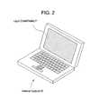
- FIG. 2is an external perspective view of a note PC.
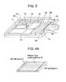
- FIG. 3is a schematic view showing the construction of the liquid crystal panel.
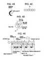
- FIG. 4(A)is a schematic view showing the construction of a main part of a reflection type liquid crystal display.
- FIGS. 4(B) to 4(E)are views for explaining a LED light source.
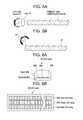
- FIGS. 5(A) and 5(B)are schematic diagrams showing the arrangement of the liquid crystal panel and the LED light source.
- FIGS. 6(A) and 6(B)are schematic diagrams showing the construction of the LED light source.
- FIGS. 7(A) to 7(F)are external views showing examples of electronic devices.
- FIGS. 1 to 7The invention will be described by referring to FIGS. 1 to 7 .
- FIG. 2shows a rough external perspective view of a note PC 20 which has a liquid crystal display 21 using a color display as a display means.
- FIG. 1(A)is an exploded perspective view of a main portion of the liquid crystal display 21 which has a scatterplate 11 and an LED light source 12 arranged in that order behind a transmission type liquid crystal panel 10 .
- an LED light source 12As an illumination light source for the transmission type liquid crystal panel 10 an LED light source 12 is used.
- the LED light source 12has LED lamps 13 arranged two dimensionally on a substrate 14 .
- FIG. 1(B)is a partial top view of the LED lamps 13 , showing the arrangement of the LED lamps 13 on the substrate 14 .
- the three-color LED lamps 13 R, 13 G, 13 Bare arranged in delta for uniform distribution over the substrate 14 .
- the scatterplate 11is made of a material transparent to a visible light, such as acrylic, polycarbonate and glass.
- the scatterplate 11may be formed at its side surface with a reflection plate.
- FIG. 3shows an outline construction of the transmission type liquid crystal panel 10 .
- An active matrix substratecomprises a pixel matrix circuit 101 , a scan line drive circuit 102 and a signal line drive circuit 103 , all formed on a glass substrate 100 .
- the scan line drive circuit 102 and the signal line drive circuit 103are connected to the pixel matrix circuit 101 through scan lines 121 and signal lines 122 .
- These drive circuits 102 , 103are formed mainly of CMOS circuits.
- the scan line 121is formed for each row of the pixel matrix circuit 101 and the signal line 122 is formed for each column of the pixel matrix circuit 101 .
- pixel TFTs 110connected to the scan lines 121 and the signal lines 122 are formed.
- the pixel TFTs 110are each connected with a pixel electrode 111 and a capacitor 112 .
- An active matrix substrate and a counter substrate 200are bonded together with a liquid crystal sealed between them.
- the active matrix substrateis formed with external terminals of TFTs during the manufacturing process, and the portions of the active matrix substrate that are formed with the external terminals are not opposed to the counter substrate 200 .
- the external terminalsare connected with an FPC (flexible printed circuit) 130 , through which external signals and power supply are fed to the circuits 101 - 103 .
- the counter substrate 200is formed with color filters at portions facing the pixel matrix circuits, and the color filters are formed with a transparent conductive film such as ITO film over the entire glass substrate.
- the transparent conductive filmis a counter electrode facing the pixel electrode 111 of the pixel matrix circuit 101 . An electric field produced between the pixel electrode 111 and the counter electrode drives the liquid crystal material.
- the active matrix substratehas IC chips 131 , 132 at the FPC 130 mounting surface. These IC chips are formed with a video signal processing circuit, a timing pulse generation circuit, a correction circuit, a memory circuit, a calculation circuit and others. Although two IC chips are shown in FIG. 3 , it is possible to use one IC chip or three or more IC chips.
- the three-color LED lamps 13 R, 13 G, 13 B of the LED light source 12are illuminated.
- the red, green and blue rays emitted from the respective LED lampsenter the scatterplate 11 where they are scattered and mixed to form white rays LW that go out from the entire surface of the scatterplate 11 .
- the white rays LWilluminate the whole back of the transmission type liquid crystal panel 10 .
- the white rays LW entering the transmission type liquid crystal panel 10are modified according to the orientation of the liquid crystal material and pass through the color filters of the counter substrate.
- the PC usercan recognize the transmitted light LT from the liquid crystal panel 10 as a color image.
- color filtersare used to produce color images, and three-color LED lamps 13 R, 13 G, 13 B are illuminated simultaneously to produce white light.
- color imagesare made without using color filters.
- One frame of a color imageis divided into three sub-frames. Red, blue and green image data are successively written into the pixel electrodes in the active matrix substrate. Then, in synchronism with the writing of red, blue and green image data, the LED lamps 13 R, 13 B, 13 G are controlled to be turned on. That is, while the red data is written, only the red LED lamp 13 R is lighted and a red image is displayed on the liquid crystal panel 10 .
- the sub-frame frequencyis 180 Hz.
- a red image, a green image and a blue imageare successively displayed. These red, green and blue images are combined on the retina of the user of PC 10 and recognized as a color image.
- a ferroelectric liquid crystal materialis appropriate for use with the liquid crystal material.
- a nematic liquid crystalit must be aligned in an optically compensated bend (OCB) mode.
- This embodimentis a variation of the embodiment 1. While in the embodiment 1 the transmission type liquid crystal panel is mounted on a note PC, this embodiment 3 describes an example of a note PC using a reflection type liquid crystal panel. The external view of the note PC is shown in FIG. 2 .
- the reflection type liquid crystal paneldoes not require a backlight and therefore has the advantages of light weight and low power consumption. However, because external light is used, the display is hard to see in a dark place. This embodiment is intended to improve this drawback.
- FIG. 4(A)shows the construction of the main part of the liquid crystal panel 10 of this embodiment.
- LED light sources 31At the opposing sides of a reflection type liquid crystal panel 30 are arranged LED light sources 31 , which illuminate the reflection type liquid crystal panel 30 so that the display can be seen even in a dark place.
- the LED light sources 31have a first-dimensionally arranged LED lamps 33 and a reflection plate 34 arranged at the back of the LED lamps 33 .
- the LED lamp 33comprises a red LED chip 33 R, a green LED chip 33 G and a blue LED chip 33 B arranged on a substrate, with the surface of these chips coated with resin 33 a .
- the surface of the resin 33 ais frosted.
- FIG. 4(E)shows an outline cross section of the reflection type liquid crystal panel 30 .
- the construction of the reflection type liquid crystal panel 30is as shown in FIG. 3 and a liquid crystal 60 is sealed between glass substrates 40 and 50 .
- the glass substrate 40 on the side of the active matrix substrateis formed with a pixel matrix circuit 41 and a peripheral drive circuit 45 .
- the pixel matrix circuit 41is formed with pixel TFTs 42 and pixel electrodes (reflective electrodes) 43 made of metal material.
- the peripheral drive circuit 45is formed mainly of CMOS circuits.
- the LED lamps 33 of the LED light sources 31are turned on.
- the red, blue and green 3-color LED chips 33 R, 33 G, 33 B of the LED lamps 33are applied with voltages to emit light.
- Light rays of red, blue and green colors emitted from the LED chips 33 R, 33 B, 33 Gare randomly scattered and mixed to form white light LW that goes out from the LED lamps 33 .
- the light that has enteredis reflected by the reflection electrodes 43 , passes through the glass substrate 50 , and leaves the liquid crystal panel.
- the reflected light LR that has penetrated the glass substrate 50is recognized as a color image by the PC user because it was modified when passing through the liquid crystal.
- the white light LWmay be collected by a lens 70 such as a cylindrical lens before entering the liquid crystal panel 30 , as shown in FIG. 5(A) .
- the LED light sources 31may be arranged diagonally above the panel to throw the white light LW onto the back (the surface formed with the inclined surfaces 50 a ) of the glass substrate 50 .
- the lens 70may be provided as shown in FIG. 5(A) .
- While this embodimentprovides two LED light sources 31 , only one light source may be used. It is also possible to arrange three or four LED light sources to encircle the liquid crystal panel 30 .
- the reflection type liquid crystal panel of the embodiment 3is shown to use color filters to display a color image, it is also possible, as in the embodiment 2, to display a color image by the reflection type liquid crystal panel without using the color filters.
- red, blue and green LEDsare turned on in succession.
- an LED lamp 90 shown in FIG. 6may preferably be used.
- the LED lamp 90 in this embodimenthas a red LED array 90 R, a green LED array 90 G and a blue LED array 90 B arranged on a substrate 90 a and coated with resin 90 b.
- the LED arrays 90 R, 90 G, 90 Bcan be turned on independently. At the timing that red, green and blue image data are written into the pixel electrodes, the corresponding color LED arrays can be turned on.
- CMOS circuits and pixel matrix circuits formed according to the inventioncan be used on a variety of electro-optical devices (active matrix type liquid crystal displays). That is, this invention can be applied to all electronic devices incorporating these direct-viewing type liquid crystal panels.
- Such electronic devicesinclude video cameras, digital cameras, head mounted displays (goggle type displays), car navigation equipment, personal computers and mobile information terminals (mobile computers, cellular phones or electronic books). Such examples are shown in FIGS. 7(A) to 7(F) .
- FIG. 7(A)shows a personal computer, which comprises a body 2001 , an image input section 2002 , a display 2003 and a keyboard 2004 .
- This inventioncan be applied to the image input section 2002 , the display 2003 and other signal control circuits.
- FIG. 7(B)shows a video camera, which comprises a body 2101 , a display 2102 , a voice input section 2103 , operation switches 2104 , a battery 2105 and a picture receiving section 2106 .
- This inventioncan be applied to the display 2102 , a voice input section 2103 and other signal control circuits.
- FIG. 7(C)shows a mobile computer, which comprises a body 2201 , a camera section 2202 , an image receiving section 2203 , an operation switch 2204 and a display 2205 .
- This inventioncan be applied to the display 2205 and other signal control circuits.
- FIG. 7(D)shows a goggle type display, which comprises a body 2301 , a display 2302 and an arm section 2303 .
- This inventioncan be applied to the display 2302 and other signal control circuits.
- FIG. 7(E)shows a player using a recording medium containing programs, which comprises a body 2401 , a display 2402 , a speaker 2403 , a recording medium 2404 , and an operation switch 2405 .
- This devicecan use DVD (digital versatile disc), CD and others as a recording medium and allows the user to listen music, see movie and perform games and Internet.
- This inventioncan be applied to the display 2402 and other signal control circuit.
- FIG. 7(F)shows a digital camera, which comprises a body 2501 , a display 2502 , an eyepiece 2503 , operation switches 2504 and an image receiving section (not shown).
- This inventioncan be applied to the display 2502 and other signal control circuits.
- the range of application of this inventionis very wide, including electronic devices in various fields which incorporate the direct-viewing type liquid crystal display. These electronic devices can be implemented by using any combination of the above embodiments 1 to 4.
- the use of the LEDs as an illuminating light source for the liquid crystal panelcan eliminate the drawbacks of a backlight using a conventional cold cathode tube, such as high power consumption and short life of the light source, and offer reduced power consumption and longer life.
Landscapes
- Physics & Mathematics (AREA)
- Nonlinear Science (AREA)
- Mathematical Physics (AREA)
- Chemical & Material Sciences (AREA)
- Crystallography & Structural Chemistry (AREA)
- General Physics & Mathematics (AREA)
- Optics & Photonics (AREA)
- Liquid Crystal (AREA)
- Devices For Indicating Variable Information By Combining Individual Elements (AREA)
- Liquid Crystal Display Device Control (AREA)
- Control Of Indicators Other Than Cathode Ray Tubes (AREA)
Abstract
Description
1. Field of the Invention
The present invention relates to electronic apparatus with a direct-viewing type liquid crystal panel which uses a light emitting diode (LED) as an illumination source for the liquid crystal panel.
The electronic apparatus of the invention include information processing devices, such as note or laptop personal computers and mobile computers, head-mounted displays, video cameras, digital still cameras, car navigation systems, and cellular phones.
2. Description of Related Art
In recent years, research and development have been conducted on the liquid crystal panel production technology and resulted in a relatively inexpensive price of the liquid crystal panel. Further, as the information society has progressed in the filed of the Internet and electronic mail, the note type personal computers (hereinafter referred to as note type PCs) have rapidly prevailed.
The digital still cameras and video cameras incorporate a liquid crystal panel so that a photographed picture can be viewed on the site. Because of this advantage, these cameras have gained popularity with consumers.
There are two types of liquid crystal panel: a transmission type and a reflection type. The transmission type liquid crystal panel has a backlight installed at the back of the panel whose illumination light passes through the liquid crystal panel to form an image on the display that can be seen by the user. The reflection type liquid crystal panel, on the other hand, does not require a backlight and forms an image by reflecting external light by the liquid crystal panel. The display quality of the reflection type, however, does not match that of the transmission type.
Because the note PCs and digital cameras are used for displaying Internet home pages in color, importance is placed on the display quality such as color reproducibility and the liquid crystal panel for use with these electronic devices needs to be of a transmission type.
Generally, the backlight source for the transmission type liquid crystal panel uses a cold cathode tube that emits white rays. The cold cathode tube is a fluorescent lamp and thus requires a high-voltage AC power supply to be turned on. Hence, the electronic devices such as note PCs require a DC-AC converter for converting a DC power supply into an AC power supply of several hundred volt.
At present, essential factors in improving the portability of electronic devices are reductions in power consumption, size and weight. Although the power consumption of the liquid crystal panel itself is small, the use of a backlight of a conventional cold cathode tube requires a high voltage, which hinders the reduction in power consumption. Another drawback is that the cold cathode tube has a short life time of about 2,000 hours.
The present invention has been accomplished in light of the problems described above and provides electronic devices incorporating a liquid crystal panel that has overcome the drawbacks of high power consumption and short longevity (life) of the light source.
In the information device incorporating a liquid crystal panel that overcomes the aforementioned drawbacks, the illuminating light source for the liquid crystal panel comprises:
3-color light emitting diodes for producing three primary colors for additive color mixing; and
a means for mixing rays from the three-color LEDs to produce white light.
In this embodiment, the use of LEDs as a light source for illuminating the liquid crystal panel makes it possible to easily reduce power consumption and size of the electronic device such as a note PC.
LED is a solid element using the photoelectric conversion effect of a semiconductor. Illuminating an LED requires application of DC voltage of about 1.5 V and thus eliminates the need for the conventional DC-AC converter, which in turn results in a significant reduction in power consumption. The LED is a semiconductor device and thus more reliable and has a smaller size and a longer life than the cold cathode tube.
In the construction described above, the 3-color LEDs for generating three primary colors for additive color mixing—typically red, green and blue LEDs—emit color rays of light which are mixed to produce white light that in turn is used for illuminating the liquid crystal panel.
The invention will be described by referring toFIGS. 1 to 7 .
This embodiment represents an example in which the present invention is applied to a note PC (personal computer) incorporating a liquid crystal display.FIG. 2 shows a rough external perspective view of a note PC20 which has aliquid crystal display 21 using a color display as a display means.
As an illumination light source for the transmission typeliquid crystal panel 10 anLED light source 12 is used. TheLED light source 12 hasLED lamps 13 arranged two dimensionally on asubstrate 14. In this embodiment, as shown inFIG. 1(B) , LED lamps of three colors—red LED lamps 13R, green LED lamps13G andblue lamps 13B—are used.FIG. 1(B) is a partial top view of theLED lamps 13, showing the arrangement of theLED lamps 13 on thesubstrate 14. The three-color LED lamps substrate 14.
Thescatterplate 11 is made of a material transparent to a visible light, such as acrylic, polycarbonate and glass. Thescatterplate 11 may be formed at its side surface with a reflection plate.
Thescan line 121 is formed for each row of thepixel matrix circuit 101 and thesignal line 122 is formed for each column of thepixel matrix circuit 101. Near the intersections of thescan lines 121 and thesignal lines 122,pixel TFTs 110 connected to thescan lines 121 and thesignal lines 122 are formed. Thepixel TFTs 110 are each connected with apixel electrode 111 and acapacitor 112.
An active matrix substrate and acounter substrate 200 are bonded together with a liquid crystal sealed between them. The active matrix substrate is formed with external terminals of TFTs during the manufacturing process, and the portions of the active matrix substrate that are formed with the external terminals are not opposed to thecounter substrate 200. The external terminals are connected with an FPC (flexible printed circuit)130, through which external signals and power supply are fed to the circuits101-103.
Thecounter substrate 200 is formed with color filters at portions facing the pixel matrix circuits, and the color filters are formed with a transparent conductive film such as ITO film over the entire glass substrate. The transparent conductive film is a counter electrode facing thepixel electrode 111 of thepixel matrix circuit 101. An electric field produced between thepixel electrode 111 and the counter electrode drives the liquid crystal material.
The active matrix substrate hasIC chips FPC 130 mounting surface. These IC chips are formed with a video signal processing circuit, a timing pulse generation circuit, a correction circuit, a memory circuit, a calculation circuit and others. Although two IC chips are shown inFIG. 3 , it is possible to use one IC chip or three or more IC chips.
In operating theliquid crystal display 21, the three-color LED lamps LED light source 12 are illuminated. The red, green and blue rays emitted from the respective LED lamps enter thescatterplate 11 where they are scattered and mixed to form white rays LW that go out from the entire surface of thescatterplate 11. The white rays LW illuminate the whole back of the transmission typeliquid crystal panel 10.
The white rays LW entering the transmission typeliquid crystal panel 10 are modified according to the orientation of the liquid crystal material and pass through the color filters of the counter substrate. The PC user can recognize the transmitted light LT from theliquid crystal panel 10 as a color image.
In the embodiment 1, color filters are used to produce color images, and three-color LED lamps
One frame of a color image is divided into three sub-frames. Red, blue and green image data are successively written into the pixel electrodes in the active matrix substrate. Then, in synchronism with the writing of red, blue and green image data, theLED lamps red LED lamp 13R is lighted and a red image is displayed on theliquid crystal panel 10.
In general, when the frequency of one frame is 60 Hz, the sub-frame frequency is 180 Hz. At this frequency a red image, a green image and a blue image are successively displayed. These red, green and blue images are combined on the retina of the user ofPC 10 and recognized as a color image.
To drive the liquid crystal at a speed as high as 180 Hz, a ferroelectric liquid crystal material is appropriate for use with the liquid crystal material. When a nematic liquid crystal is used, it must be aligned in an optically compensated bend (OCB) mode.
This embodiment is a variation of the embodiment 1. While in the embodiment 1 the transmission type liquid crystal panel is mounted on a note PC, this embodiment 3 describes an example of a note PC using a reflection type liquid crystal panel. The external view of the note PC is shown inFIG. 2 .
The reflection type liquid crystal panel does not require a backlight and therefore has the advantages of light weight and low power consumption. However, because external light is used, the display is hard to see in a dark place. This embodiment is intended to improve this drawback.
By referring toFIGS. 4(B) to 4(D) , the construction of theLED light sources 31 will be explained. As shown inFIGS. 4(B) and 4(C) , theLED light sources 31 have a first-dimensionally arrangedLED lamps 33 and a reflection plate34 arranged at the back of theLED lamps 33.
As shown inFIG. 4(D) , theLED lamp 33 comprises a red LED chip33R, agreen LED chip 33G and ablue LED chip 33B arranged on a substrate, with the surface of these chips coated withresin 33a. The surface of theresin 33ais frosted.
The function of theLED light sources 31 will be explained by referring toFIG. 4(E) .FIG. 4(E) shows an outline cross section of the reflection typeliquid crystal panel 30. The construction of the reflection typeliquid crystal panel 30 is as shown inFIG. 3 and aliquid crystal 60 is sealed betweenglass substrates glass substrate 40 on the side of the active matrix substrate is formed with apixel matrix circuit 41 and aperipheral drive circuit 45.
Thepixel matrix circuit 41 is formed withpixel TFTs 42 and pixel electrodes (reflective electrodes)43 made of metal material. Theperipheral drive circuit 45 is formed mainly of CMOS circuits.
On the back of theglass substrate 50 on the counter substrate side are formed triangular wave-shaped inclined surfaces50a. On the opposite side are formed color filters and counter electrodes.
When an image on the reflection typeliquid crystal panel 30 is to be checked in a dark place, theLED lamps 33 of theLED light sources 31 are turned on. The red, blue and green 3-color LED chips LED lamps 33 are applied with voltages to emit light. Light rays of red, blue and green colors emitted from theLED chips LED lamps 33.
The white light LW directly emitted from theLED lamps 33 or reflected by the reflection plate34 enters theglass substrate 50 on the counter substrate side from its side. Because of the inclined surfaces50aformed at the back of theglass substrate 50, the white light LW repeats being reflected as it propagates through theglass substrate 50 toward the inner part of thepanel 30. The light that has entered is reflected by thereflection electrodes 43, passes through theglass substrate 50, and leaves the liquid crystal panel. The reflected light LR that has penetrated theglass substrate 50 is recognized as a color image by the PC user because it was modified when passing through the liquid crystal.
To ensure that the white light LW can enter theglass substrate 50 efficiently, it may be collected by alens 70 such as a cylindrical lens before entering theliquid crystal panel 30, as shown inFIG. 5(A) .
Rather than arranging theLED light sources 31 horizontally with respect to theliquid crystal panel 30, they may be arranged diagonally above the panel to throw the white light LW onto the back (the surface formed with the inclined surfaces50a) of theglass substrate 50. In this case, too, thelens 70 may be provided as shown inFIG. 5(A) .
While this embodiment provides twoLED light sources 31, only one light source may be used. It is also possible to arrange three or four LED light sources to encircle theliquid crystal panel 30.
Although the reflection type liquid crystal panel of the embodiment 3 is shown to use color filters to display a color image, it is also possible, as in the embodiment 2, to display a color image by the reflection type liquid crystal panel without using the color filters.
In this case, red, blue and green LEDs are turned on in succession. Instead of using theLED lamps 33 ofFIG. 4 , anLED lamp 90 shown inFIG. 6 may preferably be used. TheLED lamp 90 in this embodiment has ared LED array 90R, agreen LED array 90G and ablue LED array 90B arranged on asubstrate 90aand coated withresin 90b.
TheLED arrays
The CMOS circuits and pixel matrix circuits formed according to the invention can be used on a variety of electro-optical devices (active matrix type liquid crystal displays). That is, this invention can be applied to all electronic devices incorporating these direct-viewing type liquid crystal panels.
Such electronic devices include video cameras, digital cameras, head mounted displays (goggle type displays), car navigation equipment, personal computers and mobile information terminals (mobile computers, cellular phones or electronic books). Such examples are shown inFIGS. 7(A) to 7(F) .
As described above, the range of application of this invention is very wide, including electronic devices in various fields which incorporate the direct-viewing type liquid crystal display. These electronic devices can be implemented by using any combination of the above embodiments 1 to 4.
The use of the LEDs as an illuminating light source for the liquid crystal panel can eliminate the drawbacks of a backlight using a conventional cold cathode tube, such as high power consumption and short life of the light source, and offer reduced power consumption and longer life.
Claims (45)
1. A method for driving a display device comprising:
a liquid crystal panel comprising:
a first substrate;
a pixel matrix circuit over the first substrate, the pixel matrix circuit comprising:
a thin film transistor over the first substrate;
an insulating film over the thin film transistor; and
a pixel electrode over the insulating film;
a liquid crystal over the pixel matrix circuit; and
an LED light source comprising a red LED array, a green LED array, a blue LED array, and a resin covering the red LED array, the green LED array, and the blue LED array,
wherein the red LED array comprises a plurality of red LED chips which are one-dimensionally arranged,
wherein the green LED array comprises a plurality of green LED chips which are one-dimensionally arranged,
wherein the blue LED array comprises a plurality of blue LED chips which are one-dimensionally arranged, and
wherein the red LED array, the green LED array, and the blue LED array are provided in parallel to one another;
the method comprising the steps of:
displaying a red image on the liquid crystal panel, comprising the steps of:
writing red image data into the pixel electrode in the pixel matrix circuit in the liquid crystal panel; and
controlling the red LED array, wherein a red light passes through the liquid crystal when the red LED array is turned on;
displaying a green image on the liquid crystal panel, comprising the steps of:
writing green image data into the pixel electrode in the pixel matrix circuit in the liquid crystal panel; and
controlling the green LED array, wherein a green light passes through the liquid crystal when the green LED array is turned on; and
displaying a blue image on the liquid crystal panel, comprising the steps of:
writing blue image data into the pixel electrode in the pixel matrix circuit in the liquid crystal panel; and
controlling the blue LED array, wherein a blue light passes through the liquid crystal when the blue LED array is turned on,
wherein the step of controlling the red LED array is in synchronism with the step of writing the red image data,
wherein the step of controlling the green LED array is in synchronism with the step of writing the green image data,
wherein the step of controlling the blue LED array is in synchronism with the step of writing the blue image data, and
wherein the step of displaying the red image, the step of displaying the green image and the step of displaying the blue image are successive.
2. The method for driving the display device according toclaim 1 ,
wherein the red image, the green image and the blue image are successively displayed, at a frequency of 180 Hz.
3. The method for driving the display device according toclaim 1 ,
wherein the liquid crystal in the liquid crystal panel is a ferroelectric liquid crystal.
4. The method for driving the display device according toclaim 1 ,
wherein the liquid crystal in the liquid crystal panel is aligned in an optically compensated bend mode.
5. The method for driving a display device according toclaim 1 , wherein the liquid crystal panel is a reflection type liquid crystal panel.
6. The method for driving a display device according toclaim 1 , wherein the liquid crystal panel further comprises a second substrate over the liquid crystal.
7. The method for driving a display device according toclaim 6 , wherein the second substrate is a glass substrate.
8. The method for driving a display device according toclaim 1 , wherein the LED light source is provided so as to face a side surface of the liquid crystal panel.
9. The method for driving a display device according toclaim 6 , wherein the LED light source is provided so that light emitted from the LED light source enters the second substrate from a side surface of the second substrate.
10. The method for driving a display device according toclaim 1 , wherein the pixel electrode is a reflective electrode.
11. The method for driving a display device according toclaim 1 , wherein each of the red light, the green light, and the blue light is reflected on the pixel electrode and emitted from the liquid crystal panel.
12. The method for driving a display device according toclaim 1 ,
wherein the red LED array, the green LED array, and the blue LED array each are coextensive with an edge of the liquid crystal panel.
13. A method for driving a display device comprising:
a liquid crystal panel comprising:
a first substrate;
a pixel matrix circuit over the first substrate, the pixel matrix circuit comprising:
a thin film transistor over the first substrate;
an insulating film over the thin film transistor; and
a pixel electrode over the insulating film;
a liquid crystal over the pixel matrix circuit; and
an LED light source comprising a red LED array, a green LED array, a blue LED array, and a resin covering the red LED array, the green LED array, and the blue LED array,
wherein the red LED array comprises a plurality of red LED chips which are one-dimensionally arranged,
wherein the green LED array comprises a plurality of green LED chips which are one-dimensionally arranged,
wherein the blue LED array comprises a plurality of blue LED chips which are one-dimensionally arranged, and
wherein the red LED array, the green LED array, and the blue LED array are provided in parallel to one another;
the method comprising the steps of:
in a first subframe period, displaying a first color image in synchronization with an emission of one of the red LED array, the green LED array, and the blue LED array;
in a second subframe period after the first subframe period, displaying a second color image in synchronization with an emission of another one of the red LED array, the green LED array, and the blue LED array; and
in a third subframe period after the second subframe period, displaying a third color image in synchronization with an emission of another one of the red LED array, the green LED array, and the blue LED array.
14. The method for driving the display device according toclaim 13 ,
wherein the liquid crystal in the liquid crystal panel is a ferroelectric liquid crystal.
15. The method for driving the display device according toclaim 13 ,
wherein the liquid crystal in the liquid crystal panel is aligned in an optically compensated bend mode.
16. The method for driving a display device according toclaim 13 , wherein the liquid crystal panel is a reflection type liquid crystal panel.
17. The method for driving a display device according toclaim 13 , wherein the liquid crystal panel further comprises a second substrate over the liquid crystal.
18. The method for driving a display device according toclaim 17 , wherein the second substrate is a glass substrate.
19. The method for driving a display device according toclaim 13 , wherein the LED light source is provided so as to face a side surface of the liquid crystal panel.
20. The method for driving a display device according toclaim 17 , wherein the LED light source is provided so that light emitted from the LED light source enters the second substrate from a side surface of the second substrate.
21. The method for driving a display device according toclaim 13 , wherein the pixel electrode is a reflective electrode.
22. The method for driving a display device according toclaim 13 ,
wherein the red LED array, the green LED array, and the blue LED array each are coextensive with an edge of the liquid crystal display panel.
23. A method for driving a display device comprising:
a liquid crystal panel comprising:
a first substrate;
a pixel matrix circuit over the first substrate, the pixel matrix circuit comprising:
a thin film transistor over the first substrate;
an insulating film over the thin film transistor; and
a pixel electrode over the insulating film;
a liquid crystal over the pixel matrix circuit; and
an LED light source comprising a red LED array, a green LED array, a blue LED array, and a resin covering the red LED array, the green LED array, and the blue LED array,
wherein the red LED array comprises a plurality of red LED chips which are one-dimensionally arranged,
wherein the green LED array comprises a plurality of green LED chips which are one-dimensionally arranged,
wherein the blue LED array comprises a plurality of blue LED chips which are one-dimensionally arranged, and
wherein the red LED array, the green LED array, and the blue LED array are provided in parallel to one another;
the method comprising the steps of:
displaying a red image on the liquid crystal panel, comprising the steps of:
writing red image data into the pixel electrode in the pixel matrix circuit in the liquid crystal panel; and
controlling the red LED array, wherein a red light passes through the liquid crystal when the red LED array is turned on;
displaying a green image on the liquid crystal panel, comprising the steps of:
writing green image data into the pixel electrode in the pixel matrix circuit in the liquid crystal panel; and
controlling the green LED array, wherein a green light passes through the liquid crystal when the green LED array is turned on; and
displaying a blue image on the liquid crystal panel, comprising the steps of:
writing blue image data into the pixel electrode in the pixel matrix circuit in the liquid crystal panel; and
controlling the blue LED array, wherein a blue light passes through the liquid crystal when the blue LED array is turned on.
24. The method for driving the display device according toclaim 23 ,
wherein the red image, the green image and the blue image are successively displayed, at a frequency of 180 Hz.
25. The method for driving the display device according toclaim 23 , wherein the liquid crystal in the liquid crystal panel is a ferroelectric liquid crystal.
26. The method for driving the display device according toclaim 23 , wherein the liquid crystal in the liquid crystal panel is aligned in an optically compensated bend mode.
27. The method for driving a display device according toclaim 23 , wherein the liquid crystal panel is a reflection type liquid crystal panel.
28. The method for driving a display device according toclaim 23 , wherein the liquid crystal panel further comprises a second substrate over the liquid crystal.
29. The method for driving a display device according toclaim 28 , wherein the second substrate is a glass substrate.
30. The method for driving a display device according toclaim 23 , wherein the LED light source is provided so as to face a side surface of the liquid crystal panel.
31. The method for driving a display device according toclaim 28 , wherein the LED light source is provided so that light emitted from the LED light source enters the second substrate from a side surface of the second substrate.
32. The method for driving a display device according toclaim 23 , wherein the pixel electrode is a reflective electrode.
33. The method for driving a display device according toclaim 23 , wherein each of the red light, the green light, and the blue light is reflected on the pixel electrode and emitted from the liquid crystal panel.
34. The method for driving a display device according toclaim 23 , wherein the red LED array, the green LED array, and the blue LED array each are coextensive with an edge of the liquid crystal display panel.
35. A method for driving a display device comprising:
a liquid crystal panel comprising:
a first substrate;
a pixel matrix circuit over the first substrate, the pixel matrix circuit comprising:
a thin film transistor over the first substrate;
an insulating film over the thin film transistor; and
a pixel electrode over the insulating film;
a liquid crystal over the pixel matrix circuit; and
an LED light source comprising a red LED array, a green LED array, a blue LED array, and a resin covering the red LED array, the green LED array, and the blue LED array,
wherein the red LED array comprises a plurality of red LED chips which are one-dimensionally arranged,
wherein the green LED array comprises a plurality of green LED chips which are one-dimensionally arranged,
wherein the blue LED array comprises a plurality of blue LED chips which are one-dimensionally arranged, and
wherein the red LED array, the green LED array, and the blue LED array are provided in parallel to one another;
the method comprising the steps of:
displaying a first color image in synchronization with an emission of one of the red LED array, the green LED array, and the blue LED array;
displaying a second color image in synchronization with an emission of another one of the red LED array, the green LED array, and the blue LED array; and
displaying a third color image in synchronization with an emission of another one of the red LED array, the green LED array, and the blue LED array.
36. The method for driving the display device according toclaim 35 , wherein the liquid crystal in the liquid crystal panel is a ferroelectric liquid crystal.
37. The method for driving the display device according toclaim 35 , wherein the liquid crystal in the liquid crystal panel is aligned in an optically compensated bend mode.
38. The method for driving a display device according toclaim 35 , wherein the liquid crystal panel is a reflection type liquid crystal panel.
39. The method for driving a display device according toclaim 35 , wherein the liquid crystal panel further comprises a second substrate over the liquid crystal.
40. The method for driving a display device according toclaim 39 , wherein the second substrate is a glass substrate.
41. The method for driving a display device according toclaim 35 , wherein the LED light source is provided so as to face a side surface of the liquid crystal panel.
42. The method for driving a display device according toclaim 39 , wherein the LED light source is provided so that light emitted from the LED light source enters the second substrate from a side surface of the second substrate.
43. The method for driving a display device according toclaim 35 , wherein the pixel electrode is a reflective electrode.
44. The method for driving a display device according toclaim 35 , wherein each of the red light, the green light, and the blue light is reflected on the pixel electrode and emitted from the liquid crystal panel.
45. The method for driving a display device according toclaim 35 , wherein the red LED array, the green LED array, and the blue LED array each are coextensive with an edge of the liquid crystal display panel.
Priority Applications (2)
| Application Number | Priority Date | Filing Date | Title |
|---|---|---|---|
| US12/249,266US8547322B2 (en) | 1998-09-03 | 2008-10-10 | Electronic device with liquid crystal display |
| US14/037,824US20140028941A1 (en) | 1998-09-03 | 2013-09-26 | Electronic device with liquid crystal display |
Applications Claiming Priority (5)
| Application Number | Priority Date | Filing Date | Title |
|---|---|---|---|
| JP10248931AJP2000081848A (en) | 1998-09-03 | 1998-09-03 | Electronic equipment mounting liquid crystal display device |
| JP10-248931 | 1998-09-03 | ||
| US09/385,020US7262754B1 (en) | 1998-09-03 | 1999-08-30 | Electronic device with liquid crystal display |
| US10/989,361US7916130B2 (en) | 1998-09-03 | 2004-11-17 | Electronic device with liquid crystal display |
| US12/249,266US8547322B2 (en) | 1998-09-03 | 2008-10-10 | Electronic device with liquid crystal display |
Related Parent Applications (1)
| Application Number | Title | Priority Date | Filing Date |
|---|---|---|---|
| US10/989,361ContinuationUS7916130B2 (en) | 1998-09-03 | 2004-11-17 | Electronic device with liquid crystal display |
Related Child Applications (1)
| Application Number | Title | Priority Date | Filing Date |
|---|---|---|---|
| US14/037,824ContinuationUS20140028941A1 (en) | 1998-09-03 | 2013-09-26 | Electronic device with liquid crystal display |
Publications (2)
| Publication Number | Publication Date |
|---|---|
| US20090058795A1 US20090058795A1 (en) | 2009-03-05 |
| US8547322B2true US8547322B2 (en) | 2013-10-01 |
Family
ID=17185556
Family Applications (5)
| Application Number | Title | Priority Date | Filing Date |
|---|---|---|---|
| US09/385,020Expired - Fee RelatedUS7262754B1 (en) | 1998-09-03 | 1999-08-30 | Electronic device with liquid crystal display |
| US10/989,361Expired - Fee RelatedUS7916130B2 (en) | 1998-09-03 | 2004-11-17 | Electronic device with liquid crystal display |
| US12/249,266Expired - Fee RelatedUS8547322B2 (en) | 1998-09-03 | 2008-10-10 | Electronic device with liquid crystal display |
| US12/249,260Expired - Fee RelatedUS8368845B2 (en) | 1998-09-03 | 2008-10-10 | Electronic device with liquid crystal display |
| US14/037,824AbandonedUS20140028941A1 (en) | 1998-09-03 | 2013-09-26 | Electronic device with liquid crystal display |
Family Applications Before (2)
| Application Number | Title | Priority Date | Filing Date |
|---|---|---|---|
| US09/385,020Expired - Fee RelatedUS7262754B1 (en) | 1998-09-03 | 1999-08-30 | Electronic device with liquid crystal display |
| US10/989,361Expired - Fee RelatedUS7916130B2 (en) | 1998-09-03 | 2004-11-17 | Electronic device with liquid crystal display |
Family Applications After (2)
| Application Number | Title | Priority Date | Filing Date |
|---|---|---|---|
| US12/249,260Expired - Fee RelatedUS8368845B2 (en) | 1998-09-03 | 2008-10-10 | Electronic device with liquid crystal display |
| US14/037,824AbandonedUS20140028941A1 (en) | 1998-09-03 | 2013-09-26 | Electronic device with liquid crystal display |
Country Status (4)
| Country | Link |
|---|---|
| US (5) | US7262754B1 (en) |
| EP (2) | EP1569029A1 (en) |
| JP (1) | JP2000081848A (en) |
| DE (1) | DE69942384D1 (en) |
Cited By (1)
| Publication number | Priority date | Publication date | Assignee | Title |
|---|---|---|---|---|
| US20140159587A1 (en)* | 2012-12-12 | 2014-06-12 | Qualcomm Mems Technologies, Inc. | Dynamic adaptive illumination control for field sequential color mode transitions |
Families Citing this family (100)
| Publication number | Priority date | Publication date | Assignee | Title |
|---|---|---|---|---|
| WO1999052006A2 (en) | 1998-04-08 | 1999-10-14 | Etalon, Inc. | Interferometric modulation of radiation |
| US8928967B2 (en) | 1998-04-08 | 2015-01-06 | Qualcomm Mems Technologies, Inc. | Method and device for modulating light |
| JP2000081848A (en)* | 1998-09-03 | 2000-03-21 | Semiconductor Energy Lab Co Ltd | Electronic equipment mounting liquid crystal display device |
| TW528169U (en)* | 2000-05-04 | 2003-04-11 | Koninkl Philips Electronics Nv | Assembly of a display device and an illumination system |
| GB0011749D0 (en) | 2000-05-17 | 2000-07-05 | Cambridge Display Tech Ltd | Light-eminating devices |
| JP2002131746A (en)* | 2000-10-25 | 2002-05-09 | Fujitsu Kiden Ltd | Backlight unit of lcd, its state detecting device and state monitoring system of display device |
| US6925313B2 (en) | 2001-02-07 | 2005-08-02 | Hyundai Curitel Inc. | Folder-type mobile communication terminal having double-sided LCD |
| US7855708B2 (en) | 2001-09-05 | 2010-12-21 | Honeywell International Inc. | LED backlight luminance sensing for LCDs |
| US7064740B2 (en)* | 2001-11-09 | 2006-06-20 | Sharp Laboratories Of America, Inc. | Backlit display with improved dynamic range |
| DE10201029A1 (en)* | 2002-01-11 | 2003-07-24 | Siemens Ag | display device |
| JP2003207770A (en)* | 2002-01-15 | 2003-07-25 | Toppan Printing Co Ltd | Color filter for liquid crystal display device and liquid crystal display device using the same |
| TW543802U (en)* | 2002-06-10 | 2003-07-21 | Shuttle Inc | Improvement of computer master panel |
| KR100939615B1 (en)* | 2002-12-13 | 2010-02-01 | 엘지디스플레이 주식회사 | Transflective liquid crystal display device with increased color reproducibility and brightness and driving method thereof |
| TWI289708B (en) | 2002-12-25 | 2007-11-11 | Qualcomm Mems Technologies Inc | Optical interference type color display |
| JP4063082B2 (en)* | 2003-01-10 | 2008-03-19 | 日本電気株式会社 | Flexible electronic device and manufacturing method thereof |
| TWI351548B (en)* | 2003-01-15 | 2011-11-01 | Semiconductor Energy Lab | Manufacturing method of liquid crystal display dev |
| US6967700B2 (en)* | 2003-11-03 | 2005-11-22 | Motorola, Inc. | Sequential full color display and photocell device |
| WO2005052673A2 (en) | 2003-11-21 | 2005-06-09 | Sharp Laboratories Of America, Inc. | Liquid crystal display with adaptive color |
| US7342705B2 (en) | 2004-02-03 | 2008-03-11 | Idc, Llc | Spatial light modulator with integrated optical compensation structure |
| US7706050B2 (en)* | 2004-03-05 | 2010-04-27 | Qualcomm Mems Technologies, Inc. | Integrated modulator illumination |
| US7612757B2 (en)* | 2004-05-04 | 2009-11-03 | Sharp Laboratories Of America, Inc. | Liquid crystal display with modulated black point |
| US7777714B2 (en)* | 2004-05-04 | 2010-08-17 | Sharp Laboratories Of America, Inc. | Liquid crystal display with adaptive width |
| US7532192B2 (en)* | 2004-05-04 | 2009-05-12 | Sharp Laboratories Of America, Inc. | Liquid crystal display with filtered black point |
| US7505018B2 (en)* | 2004-05-04 | 2009-03-17 | Sharp Laboratories Of America, Inc. | Liquid crystal display with reduced black level insertion |
| US7872631B2 (en)* | 2004-05-04 | 2011-01-18 | Sharp Laboratories Of America, Inc. | Liquid crystal display with temporal black point |
| US20050248553A1 (en)* | 2004-05-04 | 2005-11-10 | Sharp Laboratories Of America, Inc. | Adaptive flicker and motion blur control |
| US7602369B2 (en)* | 2004-05-04 | 2009-10-13 | Sharp Laboratories Of America, Inc. | Liquid crystal display with colored backlight |
| US8395577B2 (en)* | 2004-05-04 | 2013-03-12 | Sharp Laboratories Of America, Inc. | Liquid crystal display with illumination control |
| US7023451B2 (en)* | 2004-06-14 | 2006-04-04 | Sharp Laboratories Of America, Inc. | System for reducing crosstalk |
| KR20060000977A (en)* | 2004-06-30 | 2006-01-06 | 엘지.필립스 엘시디 주식회사 | Backlight Unit of LCD |
| US7556836B2 (en)* | 2004-09-03 | 2009-07-07 | Solae, Llc | High protein snack product |
| US7355780B2 (en) | 2004-09-27 | 2008-04-08 | Idc, Llc | System and method of illuminating interferometric modulators using backlighting |
| US7750886B2 (en) | 2004-09-27 | 2010-07-06 | Qualcomm Mems Technologies, Inc. | Methods and devices for lighting displays |
| US7813026B2 (en) | 2004-09-27 | 2010-10-12 | Qualcomm Mems Technologies, Inc. | System and method of reducing color shift in a display |
| US7898519B2 (en)* | 2005-02-17 | 2011-03-01 | Sharp Laboratories Of America, Inc. | Method for overdriving a backlit display |
| JP2006120355A (en)* | 2004-10-19 | 2006-05-11 | Omron Corp | Backlight device and liquid crystal display device |
| US7525528B2 (en)* | 2004-11-16 | 2009-04-28 | Sharp Laboratories Of America, Inc. | Technique that preserves specular highlights |
| US8050511B2 (en)* | 2004-11-16 | 2011-11-01 | Sharp Laboratories Of America, Inc. | High dynamic range images from low dynamic range images |
| US8050512B2 (en)* | 2004-11-16 | 2011-11-01 | Sharp Laboratories Of America, Inc. | High dynamic range images from low dynamic range images |
| KR100609057B1 (en) | 2004-11-17 | 2006-08-09 | 삼성전자주식회사 | Backlight Unit |
| WO2006082883A1 (en)* | 2005-02-03 | 2006-08-10 | Nikon Corporation | Display device, electronic device and camera |
| US20060202944A1 (en)* | 2005-03-11 | 2006-09-14 | Searete Llc, A Limited Liability Corporation Of The State Of Delaware | Elements for self assembling displays |
| US8300007B2 (en)* | 2005-03-11 | 2012-10-30 | The Invention Science Fund I, Llc | Self assembling display with substrate |
| US8390537B2 (en)* | 2005-03-11 | 2013-03-05 | The Invention Science Fund I, Llc | Method of assembling displays on substrates |
| US8334819B2 (en)* | 2005-03-11 | 2012-12-18 | The Invention Science Fund I, Llc | Superimposed displays |
| US7977130B2 (en) | 2006-08-03 | 2011-07-12 | The Invention Science Fund I, Llc | Method of assembling displays on substrates |
| US8860635B2 (en)* | 2005-04-04 | 2014-10-14 | The Invention Science Fund I, Llc | Self assembling display with substrate |
| US9153163B2 (en)* | 2005-03-11 | 2015-10-06 | The Invention Science Fund I, Llc | Self assembly of elements for displays |
| US8711063B2 (en)* | 2005-03-11 | 2014-04-29 | The Invention Science Fund I, Llc | Self assembly of elements for displays |
| JP4701806B2 (en)* | 2005-04-19 | 2011-06-15 | ソニー株式会社 | Backlight device and liquid crystal display device |
| US7916980B2 (en) | 2006-01-13 | 2011-03-29 | Qualcomm Mems Technologies, Inc. | Interconnect structure for MEMS device |
| US8121401B2 (en)* | 2006-01-24 | 2012-02-21 | Sharp Labortories of America, Inc. | Method for reducing enhancement of artifacts and noise in image color enhancement |
| US9143657B2 (en)* | 2006-01-24 | 2015-09-22 | Sharp Laboratories Of America, Inc. | Color enhancement technique using skin color detection |
| EP1832915B1 (en)* | 2006-01-31 | 2012-04-18 | Semiconductor Energy Laboratory Co., Ltd. | Display device with improved contrast |
| JP2007206326A (en)* | 2006-02-01 | 2007-08-16 | Nec Lcd Technologies Ltd | Liquid crystal display device, driving circuit and driving method used for the liquid crystal display device |
| KR100755615B1 (en)* | 2006-04-14 | 2007-09-06 | 삼성전기주식회사 | Backlight of liquid crystal display using light emitting diode |
| KR100764377B1 (en)* | 2006-04-17 | 2007-10-08 | 삼성전기주식회사 | Edge type backlight unit |
| US20080006833A1 (en)* | 2006-06-02 | 2008-01-10 | Semiconductor Energy Laboratory Co., Ltd. | Lighting device and liquid crystal display device |
| US7766498B2 (en) | 2006-06-21 | 2010-08-03 | Qualcomm Mems Technologies, Inc. | Linear solid state illuminator |
| WO2008009177A1 (en)* | 2006-07-14 | 2008-01-24 | Topson Optoelectronics Semi Co | Tapered prism illumination device for lcd backlight |
| US7845841B2 (en) | 2006-08-28 | 2010-12-07 | Qualcomm Mems Technologies, Inc. | Angle sweeping holographic illuminator |
| EP1943551A2 (en) | 2006-10-06 | 2008-07-16 | Qualcomm Mems Technologies, Inc. | Light guide |
| US8107155B2 (en) | 2006-10-06 | 2012-01-31 | Qualcomm Mems Technologies, Inc. | System and method for reducing visual artifacts in displays |
| EP2069838A2 (en) | 2006-10-06 | 2009-06-17 | Qualcomm Mems Technologies, Inc. | Illumination device with built-in light coupler |
| US7855827B2 (en) | 2006-10-06 | 2010-12-21 | Qualcomm Mems Technologies, Inc. | Internal optical isolation structure for integrated front or back lighting |
| EP1943555B1 (en) | 2006-10-06 | 2012-05-02 | QUALCOMM MEMS Technologies, Inc. | Optical loss structure integrated in an illumination apparatus of a display |
| US7864395B2 (en) | 2006-10-27 | 2011-01-04 | Qualcomm Mems Technologies, Inc. | Light guide including optical scattering elements and a method of manufacture |
| US8941580B2 (en)* | 2006-11-30 | 2015-01-27 | Sharp Laboratories Of America, Inc. | Liquid crystal display with area adaptive backlight |
| US7777954B2 (en) | 2007-01-30 | 2010-08-17 | Qualcomm Mems Technologies, Inc. | Systems and methods of providing a light guiding layer |
| US7733439B2 (en) | 2007-04-30 | 2010-06-08 | Qualcomm Mems Technologies, Inc. | Dual film light guide for illuminating displays |
| EP2015134A3 (en)* | 2007-07-13 | 2009-08-05 | TTE Indianapolis | Appearance improvement for zone backlit lcd display |
| US8354992B2 (en) | 2007-07-13 | 2013-01-15 | Tte Indianapolis | Appearance improvement for zone backlit LCD displays |
| CN101796613B (en)* | 2007-09-14 | 2012-06-27 | 株式会社半导体能源研究所 | Semiconductor devices and electronic equipment |
| US8068710B2 (en) | 2007-12-07 | 2011-11-29 | Qualcomm Mems Technologies, Inc. | Decoupled holographic film and diffuser |
| TWI368758B (en)* | 2007-12-31 | 2012-07-21 | Ind Tech Res Inst | Stereo-image displaying apparatus and method for reducing stereo-image cross-talk |
| WO2009102731A2 (en) | 2008-02-12 | 2009-08-20 | Qualcomm Mems Technologies, Inc. | Devices and methods for enhancing brightness of displays using angle conversion layers |
| US8654061B2 (en) | 2008-02-12 | 2014-02-18 | Qualcomm Mems Technologies, Inc. | Integrated front light solution |
| WO2009129264A1 (en) | 2008-04-15 | 2009-10-22 | Qualcomm Mems Technologies, Inc. | Light with bi-directional propagation |
| US8118468B2 (en) | 2008-05-16 | 2012-02-21 | Qualcomm Mems Technologies, Inc. | Illumination apparatus and methods |
| CN102047155B (en) | 2008-05-28 | 2013-04-03 | 高通Mems科技公司 | Light guide panel with light turning microstructure, its manufacturing method and display device |
| EP2307795A2 (en)* | 2008-06-04 | 2011-04-13 | QUALCOMM MEMS Technologies, Inc. | Edge shadow reducing methods for prismatic front light |
| US8358266B2 (en) | 2008-09-02 | 2013-01-22 | Qualcomm Mems Technologies, Inc. | Light turning device with prismatic light turning features |
| KR20110104090A (en) | 2009-01-13 | 2011-09-21 | 퀄컴 엠이엠스 테크놀로지스, 인크. | Large Area Light Panels and Screens |
| CN102449512A (en) | 2009-05-29 | 2012-05-09 | 高通Mems科技公司 | Illumination devices and methods of fabrication thereof |
| EP2438588A4 (en) | 2009-06-03 | 2013-01-16 | Mri Inc | Dynamic dimming led backlight |
| WO2010147005A1 (en)* | 2009-06-15 | 2010-12-23 | シャープ株式会社 | Illuminating device, display device, and television receiver |
| TWI562109B (en)* | 2010-08-05 | 2016-12-11 | Semiconductor Energy Lab Co Ltd | Driving method of liquid crystal display device |
| US8402647B2 (en) | 2010-08-25 | 2013-03-26 | Qualcomm Mems Technologies Inc. | Methods of manufacturing illumination systems |
| US8902484B2 (en) | 2010-12-15 | 2014-12-02 | Qualcomm Mems Technologies, Inc. | Holographic brightness enhancement film |
| US20130278868A1 (en)* | 2011-12-07 | 2013-10-24 | Manufacturing Resources International, Inc. | Optically Isolated Cavity For Light Sensor Feedback in LCD |
| US9348174B2 (en) | 2013-03-14 | 2016-05-24 | Manufacturing Resources International, Inc. | Rigid LCD assembly |
| US9690137B2 (en) | 2013-07-03 | 2017-06-27 | Manufacturing Resources International, Inc. | Airguide backlight assembly |
| TWI618966B (en)* | 2013-10-14 | 2018-03-21 | 元太科技工業股份有限公司 | Reflective display apparatus and manufacturing method of reflective display apparatus |
| US10191212B2 (en) | 2013-12-02 | 2019-01-29 | Manufacturing Resources International, Inc. | Expandable light guide for backlight |
| US10527276B2 (en) | 2014-04-17 | 2020-01-07 | Manufacturing Resources International, Inc. | Rod as a lens element for light emitting diodes |
| US10649273B2 (en) | 2014-10-08 | 2020-05-12 | Manufacturing Resources International, Inc. | LED assembly for transparent liquid crystal display and static graphic |
| US10261362B2 (en) | 2015-09-01 | 2019-04-16 | Manufacturing Resources International, Inc. | Optical sheet tensioner |
| JP2022156704A (en)* | 2021-03-31 | 2022-10-14 | 株式会社ジャパンディスプレイ | Communication device and communication method |
| CN115312559A (en)* | 2022-08-09 | 2022-11-08 | 江苏第三代半导体研究院有限公司 | Hybrid light source of ultraviolet and visible light and preparation method thereof |
| US12429726B1 (en) | 2023-10-02 | 2025-09-30 | Manufacturing Resources International, Inc. | Optical stack with a liquid crystal layer and a micro lens array, electronic display assembly, and related methods |
Citations (71)
| Publication number | Priority date | Publication date | Assignee | Title |
|---|---|---|---|---|
| US4445132A (en)* | 1980-06-13 | 1984-04-24 | Tokyo Shibaura Denki Kabushiki Kaisha | LED Module for a flat panel display unit |
| JPS62251723A (en) | 1986-04-25 | 1987-11-02 | Seiko Epson Corp | Driver - Built-in LCD panel |
| US4822145A (en) | 1986-05-14 | 1989-04-18 | Massachusetts Institute Of Technology | Method and apparatus utilizing waveguide and polarized light for display of dynamic images |
| US4963859A (en) | 1987-02-02 | 1990-10-16 | National Research Development Corporation | Method and apparatus for capturing information in drawing or writing |
| US4978952A (en) | 1989-02-24 | 1990-12-18 | Collimated Displays Incorporated | Flat screen color video display |
| EP0507639A2 (en) | 1991-04-05 | 1992-10-07 | Sharp Kabushiki Kaisha | A liquid crystal display device and a liquid crystal display system using the liquid crystal display device |
| US5206749A (en) | 1990-12-31 | 1993-04-27 | Kopin Corporation | Liquid crystal display having essentially single crystal transistors pixels and driving circuits |
| EP0545705A1 (en) | 1991-12-03 | 1993-06-09 | Sharp Kabushiki Kaisha | Liquid crystal display device |
| JPH05158033A (en) | 1991-12-03 | 1993-06-25 | Sharp Corp | Liquid crystal display |
| JPH05289076A (en) | 1992-04-13 | 1993-11-05 | Alps Electric Co Ltd | Liquid crystal display device |
| US5287205A (en) | 1991-03-26 | 1994-02-15 | Semiconductor Energy Laboratory Co., Ltd. | Gradation method for driving liquid crystal device with ramp and select signal |
| EP0593266A2 (en) | 1992-10-12 | 1994-04-20 | Seiko Instruments Inc. | Active matrix light valve device |
| US5334993A (en) | 1991-09-04 | 1994-08-02 | Sharp Kabushiki Kaisha | Liquid crystal display device |
| US5375043A (en) | 1992-07-27 | 1994-12-20 | Inoue Denki Co., Inc. | Lighting unit |
| JPH0720985A (en) | 1993-06-29 | 1995-01-24 | Teraoka Seiko Co Ltd | Touch panel |
| EP0659910A2 (en) | 1993-11-19 | 1995-06-28 | Mega Chips Corporation | Semiconductor device and method of fabricating the same |
| JPH07191311A (en) | 1993-12-27 | 1995-07-28 | Kokusai Electric Co Ltd | Backlight device for liquid crystal unit |
| JPH07239482A (en) | 1993-12-28 | 1995-09-12 | Kurisutaru Device:Kk | Liquid crystal display device, its production, semiconductor device and its production |
| US5453855A (en)* | 1992-12-15 | 1995-09-26 | Koito Manufacturing Co., Ltd. | Liquid crystal display device backlit by LED's coupled to printed circuit board |
| JPH07253853A (en) | 1994-03-15 | 1995-10-03 | Matsushita Electric Works Ltd | Touch panel and display device using touch panel |
| JPH07301714A (en) | 1994-05-09 | 1995-11-14 | Beam Soken:Kk | Surface light radiating device |
| JPH0850291A (en) | 1994-06-24 | 1996-02-20 | Minnesota Mining & Mfg Co <3M> | Liquid crystal display that is provided with luminance intensifying film and illuminated from front side |
| US5506598A (en)* | 1992-01-21 | 1996-04-09 | Sharp Kabushiki Kaisha | Active matrix substrate and a method for driving the same |
| US5532854A (en) | 1994-01-25 | 1996-07-02 | Fergason; James L. | Folded variable birefringerence zeroth order hybrid aligned liquid crystal apparatus |
| JPH08211361A (en) | 1995-02-06 | 1996-08-20 | Casio Electron Mfg Co Ltd | Transmissive display |
| JPH09146089A (en) | 1995-11-28 | 1997-06-06 | Masahiko Yamamoto | Surface light source for color display device and liquid crystal display device |
| JPH09172201A (en) | 1995-12-20 | 1997-06-30 | Nichia Chem Ind Ltd | Planar light emitting device and driving method thereof |
| JPH09230342A (en) | 1996-02-27 | 1997-09-05 | Rohm Co Ltd | Surface light emission illuminating device |
| US5671994A (en) | 1994-06-08 | 1997-09-30 | Clio Technologies, Inc. | Flat and transparent front-lighting system using microprisms |
| JPH1063204A (en) | 1996-08-13 | 1998-03-06 | Shichizun Denshi:Kk | Color display device |
| WO1998013709A1 (en) | 1996-09-24 | 1998-04-02 | Seiko Epson Corporation | Illuminating device and display using the device |
| US5751383A (en) | 1993-06-01 | 1998-05-12 | Sharp Kabushiki Kaisha | Image display device having a pixel multiplying means |
| US5757348A (en) | 1994-12-22 | 1998-05-26 | Displaytech, Inc. | Active matrix liquid crystal image generator with hybrid writing scheme |
| JPH10161123A (en) | 1996-10-04 | 1998-06-19 | Matsushita Electric Ind Co Ltd | Lighting device and display device |
| JPH10161113A (en) | 1996-11-26 | 1998-06-19 | Seiko Instr Inc | Display device |
| US5777594A (en) | 1995-09-13 | 1998-07-07 | Canon Kabushiki Kaisha | Liquid crystal display apparatus |
| JPH10221692A (en) | 1997-02-10 | 1998-08-21 | Nikon Corp | Display device |
| US5828429A (en) | 1991-10-16 | 1998-10-27 | Semiconductor Energy Laboratory Co., Lt.D | Electro-optical device and method of driving with voltage supply lines parallel to gate lines and two transistors per pixel |
| US5896119A (en) | 1995-06-27 | 1999-04-20 | Silicon Graphics, Inc. | Removable backlighting assembly for flat panel display subsystem |
| US5923311A (en) | 1995-12-15 | 1999-07-13 | U.S. Philips Corporation | Matrix display devices |
| US5926240A (en) | 1996-01-29 | 1999-07-20 | Hitachi, Ltd. | Liquid crystal display apparatus comprise a silicon nitride dielectric film with thickness in a range of 80mm-170mm and disposes between a reflective pixel elect and LC layer |
| US5929951A (en) | 1994-10-21 | 1999-07-27 | Canon Kabushiki Kaisha | Illumination device and display apparatus including same |
| US5953469A (en) | 1996-10-29 | 1999-09-14 | Xeotron Corporation | Optical device utilizing optical waveguides and mechanical light-switches |
| US5995189A (en) | 1995-12-21 | 1999-11-30 | Semiconductor Energy Laboratory Co., Ltd. | Liquid-crystal display device |
| US5999282A (en) | 1995-11-08 | 1999-12-07 | Victor Company Of Japan, Ltd. | Color filter and color image display apparatus employing the filter |
| US6007209A (en) | 1997-03-19 | 1999-12-28 | Teledyne Industries, Inc. | Light source for backlighting |
| US6018379A (en)* | 1995-06-13 | 2000-01-25 | Nec Corporation | Reflective LCD having a particular scattering means |
| US6025894A (en) | 1996-09-04 | 2000-02-15 | Casio Computer Co., Ltd. | Scatter control member for organic electroluminescent light source for passing light with or without scattering depending upon an incident angle |
| US6069440A (en) | 1996-07-29 | 2000-05-30 | Nichia Kagaku Kogyo Kabushiki Kaisha | Light emitting device having a nitride compound semiconductor and a phosphor containing a garnet fluorescent material |
| US6073034A (en) | 1996-10-31 | 2000-06-06 | Kopin Corporation | Wireless telephone display system |
| USRE36792E (en) | 1983-05-13 | 2000-07-25 | Seiko Epson Corporation | Color display device using light shutter and color filters |
| US6115016A (en)* | 1997-07-30 | 2000-09-05 | Fujitsu Limited | Liquid crystal displaying apparatus and displaying control method therefor |
| US6124911A (en) | 1994-07-29 | 2000-09-26 | Kabushiki Kaisha Toshiba | Reflection LCD with a counter substrate having a plurality of curved areas |
| US6166787A (en) | 1998-03-17 | 2000-12-26 | Motorola, Inc. | Optical display device having prismatic film for enhanced viewing |
| US6181311B1 (en) | 1996-02-23 | 2001-01-30 | Canon Kabushiki Kaisha | Liquid crystal color display apparatus and driving method thereof |
| US6219116B1 (en) | 1997-09-29 | 2001-04-17 | Mitsubishi Denki Kabushiki Kaisha | Liquid crystal panel device having a light guide plate with L shaped ribs |
| US6243069B1 (en) | 1997-04-22 | 2001-06-05 | Matsushita Electric Industrial Co., Ltd. | Liquid crystal display with image reading function, image reading method and manufacturing method |
| US6243068B1 (en) | 1998-05-29 | 2001-06-05 | Silicon Graphics, Inc. | Liquid crystal flat panel display with enhanced backlight brightness and specially selected light sources |
| US6266108B1 (en) | 1997-03-25 | 2001-07-24 | Sony Corporation | Reflective liquid crystal display device with a panel, a light guide plate and polarizing plate |
| US6281867B2 (en) | 1997-03-10 | 2001-08-28 | Canon Kabushiki Kaisha | Display panel and projection type display apparatus |
| US20010045927A1 (en)* | 1997-10-31 | 2001-11-29 | Matthew Zavracky | Color display with thin gap liquid crystal |
| US6326981B1 (en) | 1997-08-28 | 2001-12-04 | Canon Kabushiki Kaisha | Color display apparatus |
| US6337536B1 (en) | 1998-07-09 | 2002-01-08 | Sumitomo Electric Industries, Ltd. | White color light emitting diode and neutral color light emitting diode |
| US6340824B1 (en) | 1997-09-01 | 2002-01-22 | Kabushiki Kaisha Toshiba | Semiconductor light emitting device including a fluorescent material |
| US6384818B1 (en) | 1996-09-27 | 2002-05-07 | Semiconductor Energy Laboratory Co., Ltd. | Electrooptical device and method of fabricating the same |
| US6586874B1 (en) | 1997-05-16 | 2003-07-01 | Kabushiki Kaisha Toshiba | Image display device and light emission device |
| US6677214B1 (en) | 1993-11-19 | 2004-01-13 | Mega Chips Corporation | Semiconductor device and method of fabricating the same |
| US6734929B2 (en) | 2002-02-05 | 2004-05-11 | Alps Electric Co., Ltd. | Illumination device having a single light source and liquid crystal display device |
| US6819376B1 (en) | 1996-08-06 | 2004-11-16 | Seiko Epson Corporation | Liquid crystal display device with a light-shielding portion |
| US20090046218A1 (en) | 1998-09-03 | 2009-02-19 | Semiconductor Energy Laboratory Co., Ltd. | Electronic device with liquid crystal display |
| US20110024740A1 (en) | 2009-07-31 | 2011-02-03 | Semiconductor Energy Laboratory Co., Ltd. | Semiconductor device and manufacturing method thereof |
Family Cites Families (11)
| Publication number | Priority date | Publication date | Assignee | Title |
|---|---|---|---|---|
| US5231265A (en) | 1990-09-28 | 1993-07-27 | Balance Dynamics Corporation | Method and apparatus for the transfer of electrical power to a balancer |
| DE4104359A1 (en) | 1991-02-13 | 1992-08-20 | Implex Gmbh | CHARGING SYSTEM FOR IMPLANTABLE HOERHILFEN AND TINNITUS MASKERS |
| US5702431A (en) | 1995-06-07 | 1997-12-30 | Sulzer Intermedics Inc. | Enhanced transcutaneous recharging system for battery powered implantable medical device |
| JPH09218407A (en)* | 1995-12-05 | 1997-08-19 | Canon Inc | Illumination device and liquid crystal device including the illumination device |
| DE19617102A1 (en) | 1996-04-19 | 1997-10-23 | Michael Dr Klausing | Electronic energy supply method e.g. for pacemaker |
| DE19915487C1 (en) | 1999-04-07 | 2000-11-02 | Wampfler Ag | Device for the inductive transmission of electrical energy |
| AU4926700A (en) | 1999-06-11 | 2001-01-02 | Abb Research Ltd | Method and assembly for the wireless supply of electric energy to a number of actuators, actuator and primary winding therefor and system for a machine with a number of actuators |
| DE19946934B4 (en) | 1999-09-30 | 2011-09-29 | Ramsle Technology Group Gmbh, Llc | Module with angle sensors, non-contact energy transmission and contactless information transmission |
| JP2002198873A (en) | 2000-12-27 | 2002-07-12 | Nippon Baruufu Kk | High-frequency type remote driving apparatus |
| DE10119283A1 (en) | 2001-04-20 | 2002-10-24 | Philips Corp Intellectual Pty | System for wireless transmission of electric power, item of clothing, a system of clothing items and method for transmission of signals and/or electric power |
| KR20100097515A (en)* | 2009-02-26 | 2010-09-03 | 엘지디스플레이 주식회사 | Backlight unit for liquid crystal display device module |
- 1998
- 1998-09-03JPJP10248931Apatent/JP2000081848A/ennot_activeWithdrawn
- 1999
- 1999-08-30USUS09/385,020patent/US7262754B1/ennot_activeExpired - Fee Related
- 1999-09-02DEDE69942384Tpatent/DE69942384D1/ennot_activeExpired - Lifetime
- 1999-09-02EPEP05012260Apatent/EP1569029A1/ennot_activeWithdrawn
- 1999-09-02EPEP99117293Apatent/EP0984314B1/ennot_activeExpired - Lifetime
- 2004
- 2004-11-17USUS10/989,361patent/US7916130B2/ennot_activeExpired - Fee Related
- 2008
- 2008-10-10USUS12/249,266patent/US8547322B2/ennot_activeExpired - Fee Related
- 2008-10-10USUS12/249,260patent/US8368845B2/ennot_activeExpired - Fee Related
- 2013
- 2013-09-26USUS14/037,824patent/US20140028941A1/ennot_activeAbandoned
Patent Citations (90)
| Publication number | Priority date | Publication date | Assignee | Title |
|---|---|---|---|---|
| US4445132A (en)* | 1980-06-13 | 1984-04-24 | Tokyo Shibaura Denki Kabushiki Kaisha | LED Module for a flat panel display unit |
| USRE36792E (en) | 1983-05-13 | 2000-07-25 | Seiko Epson Corporation | Color display device using light shutter and color filters |
| JPS62251723A (en) | 1986-04-25 | 1987-11-02 | Seiko Epson Corp | Driver - Built-in LCD panel |
| US4822145A (en) | 1986-05-14 | 1989-04-18 | Massachusetts Institute Of Technology | Method and apparatus utilizing waveguide and polarized light for display of dynamic images |
| US4963859A (en) | 1987-02-02 | 1990-10-16 | National Research Development Corporation | Method and apparatus for capturing information in drawing or writing |
| US4978952A (en) | 1989-02-24 | 1990-12-18 | Collimated Displays Incorporated | Flat screen color video display |
| US5206749A (en) | 1990-12-31 | 1993-04-27 | Kopin Corporation | Liquid crystal display having essentially single crystal transistors pixels and driving circuits |
| US5287205A (en) | 1991-03-26 | 1994-02-15 | Semiconductor Energy Laboratory Co., Ltd. | Gradation method for driving liquid crystal device with ramp and select signal |
| EP0507639A2 (en) | 1991-04-05 | 1992-10-07 | Sharp Kabushiki Kaisha | A liquid crystal display device and a liquid crystal display system using the liquid crystal display device |
| US5334993A (en) | 1991-09-04 | 1994-08-02 | Sharp Kabushiki Kaisha | Liquid crystal display device |
| US5828429A (en) | 1991-10-16 | 1998-10-27 | Semiconductor Energy Laboratory Co., Lt.D | Electro-optical device and method of driving with voltage supply lines parallel to gate lines and two transistors per pixel |
| EP0545705A1 (en) | 1991-12-03 | 1993-06-09 | Sharp Kabushiki Kaisha | Liquid crystal display device |
| JPH05158033A (en) | 1991-12-03 | 1993-06-25 | Sharp Corp | Liquid crystal display |
| US5341231A (en) | 1991-12-03 | 1994-08-23 | Sharp Kabushiki Kaisha | Liquid crystal display device with edge lit lightguide reflecting light to back reflector by total internal reflection |
| US5506598A (en)* | 1992-01-21 | 1996-04-09 | Sharp Kabushiki Kaisha | Active matrix substrate and a method for driving the same |
| JPH05289076A (en) | 1992-04-13 | 1993-11-05 | Alps Electric Co Ltd | Liquid crystal display device |
| US5375043A (en) | 1992-07-27 | 1994-12-20 | Inoue Denki Co., Inc. | Lighting unit |
| EP0593266A2 (en) | 1992-10-12 | 1994-04-20 | Seiko Instruments Inc. | Active matrix light valve device |
| US6304243B1 (en) | 1992-10-12 | 2001-10-16 | Seiko Instruments Inc. | Light valve device |
| US6803886B2 (en) | 1992-10-12 | 2004-10-12 | Seiko Instruments Inc. | Light valve device |
| US5453855A (en)* | 1992-12-15 | 1995-09-26 | Koito Manufacturing Co., Ltd. | Liquid crystal display device backlit by LED's coupled to printed circuit board |
| US5751383A (en) | 1993-06-01 | 1998-05-12 | Sharp Kabushiki Kaisha | Image display device having a pixel multiplying means |
| JPH0720985A (en) | 1993-06-29 | 1995-01-24 | Teraoka Seiko Co Ltd | Touch panel |
| US5738731A (en) | 1993-11-19 | 1998-04-14 | Mega Chips Corporation | Photovoltaic device |
| EP0659910A2 (en) | 1993-11-19 | 1995-06-28 | Mega Chips Corporation | Semiconductor device and method of fabricating the same |
| US6025252A (en) | 1993-11-19 | 2000-02-15 | Mega Chips Corporation | Semiconductor device and method of fabricating the same |
| US6677214B1 (en) | 1993-11-19 | 2004-01-13 | Mega Chips Corporation | Semiconductor device and method of fabricating the same |
| US6106734A (en) | 1993-11-19 | 2000-08-22 | Mega Chips Corporation | Micromachine manufacture using gas beam crystallization |
| US6225668B1 (en) | 1993-11-19 | 2001-05-01 | Mega Chips Corporation | Semiconductor device having a single crystal gate electrode and insulation |
| US6177706B1 (en) | 1993-11-19 | 2001-01-23 | Mega Chips Corporation | Field-effect thin-film transistor device |
| US6137120A (en) | 1993-11-19 | 2000-10-24 | Mega Chips Corporation | Semiconductor device and method of fabricating the same |
| JPH07191311A (en) | 1993-12-27 | 1995-07-28 | Kokusai Electric Co Ltd | Backlight device for liquid crystal unit |
| JPH07239482A (en) | 1993-12-28 | 1995-09-12 | Kurisutaru Device:Kk | Liquid crystal display device, its production, semiconductor device and its production |
| US5532854A (en) | 1994-01-25 | 1996-07-02 | Fergason; James L. | Folded variable birefringerence zeroth order hybrid aligned liquid crystal apparatus |
| JPH07253853A (en) | 1994-03-15 | 1995-10-03 | Matsushita Electric Works Ltd | Touch panel and display device using touch panel |
| JPH07301714A (en) | 1994-05-09 | 1995-11-14 | Beam Soken:Kk | Surface light radiating device |
| US5671994A (en) | 1994-06-08 | 1997-09-30 | Clio Technologies, Inc. | Flat and transparent front-lighting system using microprisms |
| JPH0850291A (en) | 1994-06-24 | 1996-02-20 | Minnesota Mining & Mfg Co <3M> | Liquid crystal display that is provided with luminance intensifying film and illuminated from front side |
| US5608550A (en) | 1994-06-24 | 1997-03-04 | Minnesota Mining And Manufacturing Company | Front-lit liquid crystal display having brightness enhancing film with microridges which directs light through the display to a reflector |
| US5894539A (en) | 1994-06-24 | 1999-04-13 | Minnesota Mining And Manufacturing Company | Line light source having light pipe with rectangular cross-section |
| US6124911A (en) | 1994-07-29 | 2000-09-26 | Kabushiki Kaisha Toshiba | Reflection LCD with a counter substrate having a plurality of curved areas |
| US5929951A (en) | 1994-10-21 | 1999-07-27 | Canon Kabushiki Kaisha | Illumination device and display apparatus including same |
| US5757348A (en) | 1994-12-22 | 1998-05-26 | Displaytech, Inc. | Active matrix liquid crystal image generator with hybrid writing scheme |
| JPH08211361A (en) | 1995-02-06 | 1996-08-20 | Casio Electron Mfg Co Ltd | Transmissive display |
| US6018379A (en)* | 1995-06-13 | 2000-01-25 | Nec Corporation | Reflective LCD having a particular scattering means |
| US5896119A (en) | 1995-06-27 | 1999-04-20 | Silicon Graphics, Inc. | Removable backlighting assembly for flat panel display subsystem |
| US5777594A (en) | 1995-09-13 | 1998-07-07 | Canon Kabushiki Kaisha | Liquid crystal display apparatus |
| US5999282A (en) | 1995-11-08 | 1999-12-07 | Victor Company Of Japan, Ltd. | Color filter and color image display apparatus employing the filter |
| JPH09146089A (en) | 1995-11-28 | 1997-06-06 | Masahiko Yamamoto | Surface light source for color display device and liquid crystal display device |
| US5923311A (en) | 1995-12-15 | 1999-07-13 | U.S. Philips Corporation | Matrix display devices |
| JPH09172201A (en) | 1995-12-20 | 1997-06-30 | Nichia Chem Ind Ltd | Planar light emitting device and driving method thereof |
| US5995189A (en) | 1995-12-21 | 1999-11-30 | Semiconductor Energy Laboratory Co., Ltd. | Liquid-crystal display device |
| US8194224B2 (en) | 1995-12-21 | 2012-06-05 | Semiconductor Energy Laboratory Co., Ltd. | Liquid crystal display device having particular conductive layers |
| US7333172B1 (en) | 1995-12-21 | 2008-02-19 | Semiconductor Energy Laboratory Co., Ltd. | Liquid crystal display device having plurality of conductive layers between a substrate and sealing member and insulated by insulating film |
| US7394516B2 (en) | 1995-12-21 | 2008-07-01 | Semiconductor Energy Laboratory Co., Ltd. | Liquid crystal display device having a particular conductive layer |
| US7956978B2 (en) | 1995-12-21 | 2011-06-07 | Semiconductor Energy Laboratory Co., Ltd. | Liquid-crystal display device having a particular conductive layer |
| US5926240A (en) | 1996-01-29 | 1999-07-20 | Hitachi, Ltd. | Liquid crystal display apparatus comprise a silicon nitride dielectric film with thickness in a range of 80mm-170mm and disposes between a reflective pixel elect and LC layer |
| US6181311B1 (en) | 1996-02-23 | 2001-01-30 | Canon Kabushiki Kaisha | Liquid crystal color display apparatus and driving method thereof |
| US5890790A (en) | 1996-02-27 | 1999-04-06 | Rohm Co., Ltd. | Illuminator with light-emitting surface |
| JPH09230342A (en) | 1996-02-27 | 1997-09-05 | Rohm Co Ltd | Surface light emission illuminating device |
| US6069440A (en) | 1996-07-29 | 2000-05-30 | Nichia Kagaku Kogyo Kabushiki Kaisha | Light emitting device having a nitride compound semiconductor and a phosphor containing a garnet fluorescent material |
| US6819376B1 (en) | 1996-08-06 | 2004-11-16 | Seiko Epson Corporation | Liquid crystal display device with a light-shielding portion |
| JPH1063204A (en) | 1996-08-13 | 1998-03-06 | Shichizun Denshi:Kk | Color display device |
| US6025894A (en) | 1996-09-04 | 2000-02-15 | Casio Computer Co., Ltd. | Scatter control member for organic electroluminescent light source for passing light with or without scattering depending upon an incident angle |
| EP1341009A2 (en) | 1996-09-24 | 2003-09-03 | Seiko Epson Corporation | Illumination device and display device using it |
| WO1998013709A1 (en) | 1996-09-24 | 1998-04-02 | Seiko Epson Corporation | Illuminating device and display using the device |
| US6742907B2 (en) | 1996-09-24 | 2004-06-01 | Seiko Epson Corporation | Illumination device and display device using it |
| EP0878720A1 (en) | 1996-09-24 | 1998-11-18 | Seiko Epson Corporation | Illuminating device and display using the device |
| US6384818B1 (en) | 1996-09-27 | 2002-05-07 | Semiconductor Energy Laboratory Co., Ltd. | Electrooptical device and method of fabricating the same |
| JPH10161123A (en) | 1996-10-04 | 1998-06-19 | Matsushita Electric Ind Co Ltd | Lighting device and display device |
| US5953469A (en) | 1996-10-29 | 1999-09-14 | Xeotron Corporation | Optical device utilizing optical waveguides and mechanical light-switches |
| US6073034A (en) | 1996-10-31 | 2000-06-06 | Kopin Corporation | Wireless telephone display system |
| JPH10161113A (en) | 1996-11-26 | 1998-06-19 | Seiko Instr Inc | Display device |
| JPH10221692A (en) | 1997-02-10 | 1998-08-21 | Nikon Corp | Display device |
| US6281867B2 (en) | 1997-03-10 | 2001-08-28 | Canon Kabushiki Kaisha | Display panel and projection type display apparatus |
| US6007209A (en) | 1997-03-19 | 1999-12-28 | Teledyne Industries, Inc. | Light source for backlighting |
| US6266108B1 (en) | 1997-03-25 | 2001-07-24 | Sony Corporation | Reflective liquid crystal display device with a panel, a light guide plate and polarizing plate |
| US6243069B1 (en) | 1997-04-22 | 2001-06-05 | Matsushita Electric Industrial Co., Ltd. | Liquid crystal display with image reading function, image reading method and manufacturing method |
| US6586874B1 (en) | 1997-05-16 | 2003-07-01 | Kabushiki Kaisha Toshiba | Image display device and light emission device |
| US6115016A (en)* | 1997-07-30 | 2000-09-05 | Fujitsu Limited | Liquid crystal displaying apparatus and displaying control method therefor |
| US6326981B1 (en) | 1997-08-28 | 2001-12-04 | Canon Kabushiki Kaisha | Color display apparatus |
| US6340824B1 (en) | 1997-09-01 | 2002-01-22 | Kabushiki Kaisha Toshiba | Semiconductor light emitting device including a fluorescent material |
| US6219116B1 (en) | 1997-09-29 | 2001-04-17 | Mitsubishi Denki Kabushiki Kaisha | Liquid crystal panel device having a light guide plate with L shaped ribs |
| US20010045927A1 (en)* | 1997-10-31 | 2001-11-29 | Matthew Zavracky | Color display with thin gap liquid crystal |
| US6166787A (en) | 1998-03-17 | 2000-12-26 | Motorola, Inc. | Optical display device having prismatic film for enhanced viewing |
| US6243068B1 (en) | 1998-05-29 | 2001-06-05 | Silicon Graphics, Inc. | Liquid crystal flat panel display with enhanced backlight brightness and specially selected light sources |
| US6337536B1 (en) | 1998-07-09 | 2002-01-08 | Sumitomo Electric Industries, Ltd. | White color light emitting diode and neutral color light emitting diode |
| US20090046218A1 (en) | 1998-09-03 | 2009-02-19 | Semiconductor Energy Laboratory Co., Ltd. | Electronic device with liquid crystal display |
| US6734929B2 (en) | 2002-02-05 | 2004-05-11 | Alps Electric Co., Ltd. | Illumination device having a single light source and liquid crystal display device |
| US20110024740A1 (en) | 2009-07-31 | 2011-02-03 | Semiconductor Energy Laboratory Co., Ltd. | Semiconductor device and manufacturing method thereof |
Non-Patent Citations (23)
| Title |
|---|
| A. Tanaka, "Trends of Backlighting and Frontlighting Systems for LCD," pp. 347-350, 1998, Fujitsu Kasei Limited Planning and Development Division. |
| Bryning et al., "37.4: Reverse-Emulsion Electrophoretic Display (REED)," pp. 1018-1021, 1998, SID Digest. |
| European Office Action (Application No. 05012260.5) Dated Nov. 2, 2011. |
| European Patent Office, Search Report, Mar. 8, 2001, 3 pages. |
| European Search Report (Application No. 99117293.3) Dated Mar. 8, 2001. |
| European Search Report of Jun. 30, 2005 for EP Application No. 05 012 260.5. |
| H. J. Cornelissen et al., "Frontlights for Reflective LCDs Based on Lightguides with Micro-Grooves," SID 99 Digest, 1999, pp. 912-915. |
| Howard et al., "37.2: Gyricon Electric Paper," pp. 1010-1013, 1998, SID Digest. |
| Miyashita et al., "Full Color Liquid Crystal Display in a Field Sequential Utilizing a High Speed Response Characteristics of OCB Liquid Crystal," Liquid Crystal Society: LCD Forum Sponsorship, 1998, pp. 7-15. |
| Nakamura et al., "37.3: Development of Electrophoretic Display Using Microcapsulated Suspension," pp. 1014-1017, 1998, SID Digest. |
| Notice of Allowance (U.S. Appl. No. 12/249,260) dated Sep. 28, 2012. |
| Office Action (Application No. 05012260.5) Dated Oct. 10, 2008. |
| Office Action (European Application No. 05012260.5) dated Nov. 5, 2007. |
| Office Action (U.S. Appl. No. 12/249,260) dated Apr. 24, 2012. |
| Office Action (U.S. Appl. No. 12/249,260) dated Apr. 28, 2010. |
| Office Action (U.S. Appl. No. 12/249,260) dated Dec. 27, 2011. |
| Office Action (U.S. Appl. No. 12/249,260) dated Feb. 10, 2011. |
| Office Action (U.S. Appl. No. 12/249,260) dated Jun. 18, 2010. |
| Okita, M., "Field Sequential Full Color LCD," Monthly Display, Jul. 1998, Separate Edition, pp. 11-16 and News Flash. |
| Okita.M, "Field Sequential Full Color LCD Without Color Filter,", Field Sequential Full Color LCD (Monthly Display Separate Edition), Jul. 1, 1998, pp. 11-16. |
| Tai et al., "24.1: A Transparent Frontlighting System for Reflective-Type Displays," pp. 375-378, 1995, SID Digest. |
| Tanaka.A, "Trends of Backlighting and Frontlighting Systems for LCD,", IDW '98 : Proceedings of the 5th International Display Workshops, Dec. 7, 1998, pp. 347-350. |
| Tatsuaki Funamoto et al., "A Front-lighting System Utilizing a Thin Light Guide," Asia Display, 1998, pp. 897-900. |
Cited By (1)
| Publication number | Priority date | Publication date | Assignee | Title |
|---|---|---|---|---|
| US20140159587A1 (en)* | 2012-12-12 | 2014-06-12 | Qualcomm Mems Technologies, Inc. | Dynamic adaptive illumination control for field sequential color mode transitions |
Also Published As
| Publication number | Publication date |
|---|---|
| US7916130B2 (en) | 2011-03-29 |
| DE69942384D1 (en) | 2010-07-01 |
| US20140028941A1 (en) | 2014-01-30 |
| US7262754B1 (en) | 2007-08-28 |
| US20050088403A1 (en) | 2005-04-28 |
| EP0984314A3 (en) | 2001-04-25 |
| EP0984314B1 (en) | 2010-05-19 |
| EP1569029A1 (en) | 2005-08-31 |
| JP2000081848A (en) | 2000-03-21 |
| EP0984314A2 (en) | 2000-03-08 |
| US20090046218A1 (en) | 2009-02-19 |
| US8368845B2 (en) | 2013-02-05 |
| US20090058795A1 (en) | 2009-03-05 |
Similar Documents
| Publication | Publication Date | Title |
|---|---|---|
| US8547322B2 (en) | Electronic device with liquid crystal display | |
| US7782421B2 (en) | Liquid crystal display device | |
| US7537357B2 (en) | Backlight unit for dynamic image and display employing the same | |
| US4842378A (en) | Method of illuminating flat panel displays to provide CRT appearing displays | |
| JP3215913B2 (en) | Display control method of liquid crystal display device and liquid crystal display device | |
| KR101296703B1 (en) | Video and content controlled backlight | |
| CN100414394C (en) | Liquid crystal display and method of illuminating the liquid crystal display | |
| JP2000081848A5 (en) | Liquid crystal display devices and mobile phones equipped with them, notebook personal computers, digital still cameras, car navigation systems, and information processing devices. | |
| KR20050107033A (en) | A light emitting diode module and a liquid crystal display provided with the same | |
| JP2006339148A (en) | Backlight unit and liquid crystal display device | |
| US8432351B2 (en) | Driving system for matrix type backlight module | |
| CN1172282C (en) | Electro-optical panels and electronic equipment | |
| WO2010147062A1 (en) | Display device | |
| JP2006190679A (en) | Backlight assembly from which dark part is removed, and display device including the same | |
| KR20130024148A (en) | Display apparatus | |
| TWI345655B (en) | Liquid crystal display device and method of modulating backlight | |
| JP2006139020A (en) | Electro-optical device and electronic apparatus | |
| US20080117159A1 (en) | Method for driving liquid crystal display with scanning backlight module | |
| KR20100049826A (en) | Liquid crystal display device | |
| KR20110083121A (en) | Televisions, Light Source Drives, and Power Supplies | |
| KR20080106677A (en) | Backlight unit and liquid crystal display device having same | |
| KR20240104962A (en) | Back Light Unit and Liquid Crystal Display Device | |
| JP2003140562A (en) | Display device | |
| KR20050115463A (en) | A liquid crystal display for improving brightness thereof | |
| KR20070067958A (en) | Driving method of liquid crystal display |
Legal Events
| Date | Code | Title | Description |
|---|---|---|---|
| STCF | Information on status: patent grant | Free format text:PATENTED CASE | |
| FEPP | Fee payment procedure | Free format text:PAYOR NUMBER ASSIGNED (ORIGINAL EVENT CODE: ASPN); ENTITY STATUS OF PATENT OWNER: LARGE ENTITY | |
| CC | Certificate of correction | ||
| FPAY | Fee payment | Year of fee payment:4 | |
| FEPP | Fee payment procedure | Free format text:MAINTENANCE FEE REMINDER MAILED (ORIGINAL EVENT CODE: REM.); ENTITY STATUS OF PATENT OWNER: LARGE ENTITY | |
| LAPS | Lapse for failure to pay maintenance fees | Free format text:PATENT EXPIRED FOR FAILURE TO PAY MAINTENANCE FEES (ORIGINAL EVENT CODE: EXP.); ENTITY STATUS OF PATENT OWNER: LARGE ENTITY | |
| STCH | Information on status: patent discontinuation | Free format text:PATENT EXPIRED DUE TO NONPAYMENT OF MAINTENANCE FEES UNDER 37 CFR 1.362 | |
| FP | Lapsed due to failure to pay maintenance fee | Effective date:20211001 |