US8542010B2 - Circuits and methods for generating a diagnostic mode of operation in a magnetic field sensor - Google Patents
Circuits and methods for generating a diagnostic mode of operation in a magnetic field sensorDownload PDFInfo
- Publication number
- US8542010B2 US8542010B2US12/840,324US84032410AUS8542010B2US 8542010 B2US8542010 B2US 8542010B2US 84032410 AUS84032410 AUS 84032410AUS 8542010 B2US8542010 B2US 8542010B2
- Authority
- US
- United States
- Prior art keywords
- magnetic field
- diagnostic
- sensing elements
- signal
- field sensor
- Prior art date
- Legal status (The legal status is an assumption and is not a legal conclusion. Google has not performed a legal analysis and makes no representation as to the accuracy of the status listed.)
- Active, expires
Links
Images


Classifications
- G—PHYSICS
- G01—MEASURING; TESTING
- G01R—MEASURING ELECTRIC VARIABLES; MEASURING MAGNETIC VARIABLES
- G01R33/00—Arrangements or instruments for measuring magnetic variables
- G01R33/0023—Electronic aspects, e.g. circuits for stimulation, evaluation, control; Treating the measured signals; calibration
- G01R33/0035—Calibration of single magnetic sensors, e.g. integrated calibration
- G—PHYSICS
- G01—MEASURING; TESTING
- G01R—MEASURING ELECTRIC VARIABLES; MEASURING MAGNETIC VARIABLES
- G01R33/00—Arrangements or instruments for measuring magnetic variables
- G01R33/0017—Means for compensating offset magnetic fields or the magnetic flux to be measured; Means for generating calibration magnetic fields
- G—PHYSICS
- G01—MEASURING; TESTING
- G01R—MEASURING ELECTRIC VARIABLES; MEASURING MAGNETIC VARIABLES
- G01R35/00—Testing or calibrating of apparatus covered by the other groups of this subclass
- G01R35/005—Calibrating; Standards or reference devices, e.g. voltage or resistance standards, "golden" references
Definitions
- This inventionrelates generally to magnetic field sensors and, more particularly, to magnetic field sensors having bother a normal mode of operation and a diagnostic mode of operation.
- magnetic field sensing elementsincluding, but not limited to, Hall effect elements, magnetoresistance elements, and magnetotransistors.
- Hall effect elementsfor example, planar Hall elements, vertical Hall elements, and circular Hall elements.
- magnetoresistance elementsfor example, anisotropic magnetoresistance (AMR) elements, giant magnetoresistance (GMR) elements, tunneling magnetoresistance (TMR) elements, Indium antimonide (InSb) elements, and magnetic tunnel junction (MTJ) elements.
- AMRanisotropic magnetoresistance
- GMRgiant magnetoresistance
- TMRtunneling magnetoresistance
- InSbIndium antimonide
- MTJmagnetic tunnel junction
- Hall effect elementsgenerate an output voltage proportional to a magnetic field.
- magnetoresistance elementschange resistance in proportion to a magnetic field.
- an electrical currentcan be directed through the magnetoresistance element, thereby generating a voltage output signal proportional to the magnetic field.
- Magnetic field sensorswhich use magnetic field sensing elements, are used in a variety of applications, including, but not limited to, a current sensor that senses a magnetic field generated by a current carried by a current-carrying conductor, a magnetic switch (also referred to herein as a proximity detector) that senses the proximity of a ferromagnetic or magnetic object, a rotation detector that senses passing ferromagnetic articles, for example, gear teeth, and a magnetic field sensor that senses a magnetic field density of a magnetic field.
- a current sensorthat senses a magnetic field generated by a current carried by a current-carrying conductor
- a magnetic switchalso referred to herein as a proximity detector
- a rotation detectorthat senses passing ferromagnetic articles, for example, gear teeth
- magnetic field sensorthat senses a magnetic field density of a magnetic field.
- Magnetic switchesare used as examples herein. However, the circuits and techniques described herein apply also to any magnetic field sensor.
- a built-in self-testis a function that can verify all or a portion of the internal functionality of an integrated circuit.
- Some types of integrated circuitshave built-in self-test circuits built directly onto the integrated circuit die.
- the built-in self-testis activated by external means, for example, a signal communicated from outside the integrated circuit to dedicated pins or ports on the integrated circuit.
- an integrated circuit that has a memory portioncan include a built-in self-test circuit, which can be activated by a self-test signal communicated from outside the integrated circuit.
- the built-in self-test circuitcan test the memory portion of the integrated circuit in response to the self-test signal.
- the present inventionprovides built-in self-test (diagnostic) circuits and techniques in a magnetic field sensor that allow the self-test to test a magnetic field sensing element used within the magnetic field sensor.
- the present inventionprovides built in self-test circuits and techniques in a magnetic field sensor that allow the self-test all of the circuits within the magnetic field sensor.
- the present inventionalso provides built in self-test circuits and techniques in a magnetic field sensor that are able to perform the self-test regardless of a magnitude of an external magnetic field.
- a magnetic field sensorincludes at least two magnetic field sensing elements.
- the magnetic field sensoralso includes a switching circuit coupled to the at least two magnetic field sensing elements.
- the switching circuitis configured to couple the at least two magnetic field sensing elements into a normal mode configuration when the magnetic field sensor is in a normal mode of operation, and the switching circuit is configured to couple the at least two magnetic field sensing elements into a diagnostic mode configuration when the magnetic field sensor is in a diagnostic mode of operation.
- the at least two magnetic field sensing elementsare configured to generate a magnetic field signal including a measured-magnetic-field-responsive signal portion responsive to a measured magnetic field when coupled in the normal mode configuration, and a diagnostic-magnetic-field-responsive signal portion responsive to a diagnostic magnetic field when coupled in the diagnostic mode configuration.
- a method of generating a self-test of a magnetic field sensorincludes coupling at least two magnetic field sensing elements into a normal mode configuration when the magnetic field sensor is in a normal mode of operation, and coupling the at least two magnetic field sensing elements into a diagnostic mode configuration when the magnetic field sensor is in a diagnostic mode of operation.
- the at least two magnetic field sensing elementsare configured to generate a magnetic field signal including a measured-magnetic-field-responsive signal portion responsive to a measured magnetic field when coupled in the normal mode configuration, and a diagnostic-magnetic-field-responsive signal portion responsive to a diagnostic magnetic field when coupled in the diagnostic mode configuration.
- FIG. 1is a block diagram of a prior art magnetic field sensor, and, in particular a magnetic switch that has a chopped (or switched) Hall effect element, and an associated switching circuit;
- FIG. 1Ais a series of graphs showing frequency spectrums at various points in the prior at magnetic field sensor of FIG. 1 ;
- FIG. 2is a block diagram showing a switched Hall element having a Hall effect element and having a switching circuit that can be used as the Hall effect element and the switching circuit of the magnetic field sensor of FIG. 1 , and also as the Hall effect element and the switching circuit of magnetic field sensors below;
- FIG. 2Ais a graph showing clock signals for the switched Hall element of FIG. 2 ;
- FIG. 2Bis a graph showing a modulated offset component provided by the switched Hall element of FIG. 2 ;
- FIG. 2Cis a graph showing an un-modulated magnetic field signal component provided by the switched Hall element of FIG. 2 ;
- FIG. 3is a block diagram showing a switched Hall element having a Hall effect element and having a switching circuit that can be used as the Hall effect element and the switching circuit in the sensor of FIG. 1 , and also as the Hall effect element and the switching circuit of magnetic field sensors below;
- FIG. 3Ais a graph showing clock signals for the switched Hall element of FIG. 3 ;
- FIG. 3Bis a graph showing an un-modulated offset component provided by the switched Hall element of FIG. 3 ;
- FIG. 3Cis a graph showing a modulated magnetic field signal component provided by the switched Hall element of FIG. 3 ;
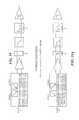
- FIG. 4is a pictorial showing a plurality of magnetic field sensor used in a gear shifting arrangement in an automobile
- FIG. 5is a block diagram showing two Hall effect elements arranged in parallel in a normal mode configuration, which would tend to respond in cooperation in the presence of an external magnetic field;
- FIG. 6is a block diagram showing the two Hall effect elements of FIG. 5 , reconnected so as to be in a diagnostic mode configuration, and in the presence of the external magnetic field of FIG. 5 and also in the presence of a two diagnostic magnetic fields as may be generated in two opposite directions, e.g., by two respective coils;
- FIG. 6Ais a block diagram showing the two Hall effect elements of FIG. 5 , reconnected so as to be in the diagnostic mode configuration, and in the presence of the external magnetic field of FIG. 5 , and also in the presence of a two diagnostic magnetic fields as may be generated in two opposite directions, e.g., by two respective coils, wherein the two diagnostic magnetic fields are AC magnetic fields;
- FIG. 7is a block diagram of a magnetic field sensor, and, in particular, a magnetic switch that has two Hall effect elements coupled in parallel as in FIG. 5 , which are together chopped (or switched) Hall effect elements, and an associated switching circuit, all operating in a normal mode of operation;
- FIG. 7Ais a series of graphs showing frequency spectrums of signals at various points in the magnetic field sensor of FIG. 7 ;
- FIG. 8is a block diagram of the magnetic field sensor of FIG. 7 , and, in particular, the magnetic switch that has the two Hall effect elements but reconfigured so as to be in the diagnostic mode configuration of FIG. 6 or 6 A, and including two coils for generating the diagnostic magnetic fields in opposite directions as indicated in FIG. 6A , all operating in a first version diagnostic mode of operation;
- FIG. 8Ais a series of graphs showing frequency spectrums of signals at various points in the magnetic field sensor of FIG. 8 ;
- FIG. 8Bis a block diagram of the magnetic field sensor of FIGS. 7 and 8 , and, in particular, the magnetic switch that has the two Hall effect elements but reconfigured so as to be in the diagnostic mode configuration of FIG. 6 or 6 A, and including the two coils for generating the diagnostic magnetic fields in opposite directions as indicated in FIG. 6A , all operating in a second version diagnostic mode of operation;
- FIG. 8Cis a series of graphs showing frequency spectrums of signals at various points in the magnetic field sensor of FIG. 8B ;
- FIG. 8Dis a block diagram of the magnetic field sensor of FIGS. 7 , 8 , and 8 B, and, in particular, the magnetic switch that has the two Hall effect elements but reconfigured so as to be in the diagnostic mode configuration of FIG. 6 or 6 A, and including the two coils for generating the diagnostic magnetic fields in opposite directions as indicated in FIG. 6A , all operating in a third version diagnostic mode of operation;
- FIG. 8Eis a series of graphs showing frequency spectrums of signals at various points in the magnetic field sensor of FIG. 8D ;
- FIG. 8Fis a block diagram of the magnetic field sensor of FIGS. 7 , 8 , 8 B, and 8 D, and, in particular, the magnetic switch that has the two Hall effect elements but reconfigured so as to be in the diagnostic mode configuration of FIG. 6 or 6 A, and including the two coils for generating the diagnostic magnetic fields in opposite directions as indicated in FIG. 6A , all operating in a fourth version diagnostic mode of operation;
- FIG. 8Gis a series of graphs showing frequency spectrums of signals at various points in the magnetic field sensor of FIG. 8F ;
- FIG. 9is a block diagram showing two Hall effect elements, most types of which have a maximum response axis perpendicular to the page, and a conductor carrying a current to generate the diagnostic magnetic fields in opposite directions proximate to the Hall effect elements;
- FIG. 9Ais a block diagram showing two Hall effect elements and another conductor carrying a current to generate the diagnostic magnetic fields in opposite directions proximate to the Hall effect elements;
- FIG. 9Bis a block diagram showing two Hall effect elements and two respective conductive coils carrying a current to generate the diagnostic magnetic fields in opposite directions proximate to the Hall effect elements;
- FIG. 10is a schematic drawing showing two magnetoresistance elements coupled in series in a normal mode configuration, which would tend to act in cooperation in response to an external magnetic field in a particular direction;
- FIG. 10Ais a schematic drawing showing two magnetoresistance elements coupled in parallel in another normal mode configuration, which would tend to act in cooperation to an external magnetic field in a particular direction;
- FIG. 10Bis a schematic drawing showing two magnetoresistance elements, reconnected so as to be in a diagnostic mode configuration
- FIG. 11is a block diagram showing two magnetoresistance elements, most types of which have a maximum response axis parallel to the page, and a conductor carrying a current to generate the diagnostic magnetic fields in opposite directions proximate to the magnetoresistance elements;
- FIG. 11Ais a block diagram showing two magnetoresistance elements and two respective conductive coils carrying a current to generate the diagnostic magnetic fields in opposite directions proximate to the magnetoresistance elements;
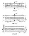
- FIG. 12is block diagram showing a cross section representative of one exemplary arrangement of one of the magnetic field sensing elements and one of the coils of FIG. 9B , wherein the arrangement includes an electromagnetic shield;
- FIG. 12Ais block diagram showing a cross section representative of another exemplary arrangement of one of the magnetic field sensing elements and one of the coils of FIG. 9B , wherein the arrangement includes an electromagnetic shield;
- FIG. 12Bis block diagram showing a cross section representative of one exemplary arrangement of one of the magnetic field sensing elements and one of the coils of FIG. 11A ;
- FIG. 12Cis block diagram showing a cross section representative of one exemplary arrangement of one of the magnetic field sensing elements and the conductor of FIG. 11 , wherein the arrangement includes an electromagnetic shield;
- FIG. 12Dis block diagram showing a cross section representative of yet another exemplary arrangement of one of the magnetic field sensing elements and the conductor of FIG. 11 , wherein the arrangement includes an electromagnetic shield;
- FIGS. 12E-12Gare block diagrams showing three arrangements for magnetic field sensors
- FIG. 13is a top view of an exemplary electromagnetic shield that can form part of the magnetic field sensor of FIGS. 7 , 8 , 8 B, 8 D, and 8 F, and which can be used as the electromagnetic shield of FIGS. 12 , 12 A, 12 C, and 12 D;
- FIG. 14is a top view of another exemplary electromagnetic shield that can form part of the magnetic field sensor of FIGS. 7 , 8 , 8 B, 8 D, and 8 F, and which can be used as the electromagnetic shield of FIGS. 12 , 12 A, 12 C, and 12 D;
- FIG. 15is a top view of yet another exemplary electromagnetic shield that can form part of the magnetic field sensor of FIGS. 7 , 8 , 8 B, 8 D, and 8 F, and which can be used as the electromagnetic shield of FIGS. 12 , 12 A, 12 C, and 12 D;
- FIG. 16is a top view of yet another exemplary electromagnetic shield that can form part of the magnetic field sensor of FIGS. 7 , 8 , 8 B, 8 D, and 8 F, and which can be used as the electromagnetic shield of FIGS. 12 , 12 A, 12 C, and 12 D,
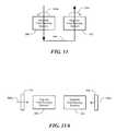
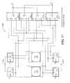
- FIG. 17is a schematic drawing showing two Hall effect elements and a switching arrangement that can achieve a reconfiguration from the normal mode configuration for FIG. 5 to the diagnostic mode configuration of FIGS. 6 of 6 A;
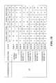
- FIG. 18is a chart showing switch positions of FIG. 17 in the normal mode of operation represented by of FIG. 7 , the first version diagnostic mode of operation represented by FIGS. 8 and 8A , the second version diagnostic mode of operation represented by FIGS. 8B and 8C , the third version diagnostic mode of operation represented by FIGS. 8D and 8E , and the fourth version diagnostic mode of operation represented by FIGS. 8F and 8G ;
- FIGS. 19 and 19Aare schematic diagrams showing the circuit of FIG. 7 showing switch positions of FIG. 17 used in a normal mode of operation;
- FIGS. 20 and 20Aare schematic diagrams representative of the circuit of FIG. 7 showing switch positions of FIG. 17 generally used in a diagnostic mode of operation;
- FIGS. 21 and 21Aare schematic diagrams showing the circuit of FIG. 8 showing switch positions of FIG. 17 used in the first version diagnostic mode of operation;
- FIGS. 22 and 22Aare schematic diagrams showing the circuit of FIG. 8B showing switch positions of FIG. 17 used in the second version diagnostic mode of operation;
- FIGS. 23 and 23Aare schematic diagrams showing the circuit of FIG. 8D showing switch positions of FIG. 17 used in the third version diagnostic mode of operation.
- FIGS. 24 and 24Aare schematic diagrams showing the circuit of FIG. 8F showing switch positions of FIG. 17 used in the fourth version diagnostic mode of operation.
- magnetic field sensing elementis used to describe a variety of types of electronic elements that can sense a magnetic field.
- the magnetic field sensing elementscan be, but are not limited to, Hall effect elements, magnetoresistance elements, or magnetotransistors.
- Hall effect elementsfor example, planar Hall elements, vertical Hall elements, and circular Hall elements.
- magnetoresistance elementsfor example, anisotropic magnetoresistance (AMR) elements, giant magnetoresistance (GMR) elements, tunneling magnetoresistance (TMR) elements, Indium antimonide (InSb) elements, and magnetic tunnel junction (MTJ) elements.
- AMRanisotropic magnetoresistance
- GMRgiant magnetoresistance
- TMRtunneling magnetoresistance
- Indium antimonide (InSb) elementsIndium antimonide
- MTJmagnetic tunnel junction
- some of the above-described magnetic field sensing elementstends to have an axis of maximum sensitivity parallel to a substrate that supports the magnetic field sensing element, and others of the above-described magnetic field sensing elements tend to have an axis of maximum sensitivity perpendicular to a substrate that supports the magnetic field sensing element.
- most, but not all, types of magnetoresistance elementstend to have axes of maximum sensitivity parallel to the substrate and most, but not all, types of Hall elements tend to have axes of sensitivity perpendicular to a substrate.
- magnetic field sensoris used to describe a circuit that includes a magnetic field sensing element.
- Magnetic field sensorsare used in a variety of applications, including, but not limited to, a current sensor that senses a magnetic field generated by a current carried by a current-carrying conductor, a magnetic switch (also referred to herein as a proximity detector) that senses the proximity of a ferromagnetic or magnetic object, a rotation detector that senses passing ferromagnetic articles, for example, gear teeth, and a magnetic field sensor that senses a magnetic field density of a magnetic field.
- Magnetic switchesproximity detectors
- the circuits and techniques described hereinapply also to any magnetic field sensor capable of detecting a magnetic field.
- magnetic field signalis used to describe any circuit signal that results from a magnetic field experienced by a magnetic field sensing element.
- Diagnostic modes of operation described beloware generally indicative of a functioning versus a non-functioning magnetic field sensor. Namely, if no output signal is generated during a diagnostic mode of operation (or, in the case of a linear magnetic field sensor, the output signal is too low or too high), the magnetic field sensor is deemed to have failed. However, while diagnostic modes of operation are described below that are indicative of a functioning versus a non-functioning magnetic field sensor, it should be appreciated that similar techniques can be used to measure a sensitivity of the magnetic field sensor or to perform a calibration of the magnetic field sensor. Thus, as used herein, the term “diagnostic” is used to encompass sensitivity measurement and calibration.
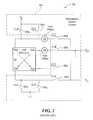
- a prior art magnetic field sensor 10includes a Hall effect element 13 coupled within a switching circuit 12 .
- the switching circuit 12is configured to generate a differential output signal 12 a , 12 b responsive to an external magnetic field.
- Many signals described belowcan be differential signals, however, the term differential is not used in all instances. In other embodiments, some or all of the signals are single ended signals.
- the switching circuit 12is more fully described below in conjunction with FIGS. 3-3C . Let it suffice here to say that the switching circuit 12 switches a drive signal (not shown) to the Hall effect element 12 with a clock at a frequency of f c
- the magnetic field sensor 10also includes a switching circuit 14 coupled to receive the signal 12 a , 12 b and configured to generate a chopped signal 14 a , 14 b .
- the switching circuit 14is also switched with the clock at a frequency of f c . Operation of the switching circuit 14 is also described more fully below in conjunction with FIGS. 3-3C .
- An amplifier 16is coupled to receive the chopped signal 14 a , 14 b and configured to generate an amplified signal 16 a , 16 b .
- a switching circuit 18is coupled to receive the amplified signal 16 a , 16 b and configured to generate a demultiplexed signal 18 a , 18 b .
- the switching circuit 18is clocked with the clock at the frequency, f c .
- a low pass filter 20is coupled to receive the demultiplexed signal 18 a , 18 b and configured to generate a filtered signal 20 a , 20 b .
- a sinx/x (sine) filter 22is coupled to receive the filtered signal 20 a , 20 b and configured to generate a filtered signal 22 a , 22 b .
- a comparator 24here a Schmitt trigger 24 , is coupled to receive the filtered signal 22 a , 22 b and configured to generate a magnetic field sensor output signal 24 a.
- the sine filter 22is a switched capacitor filter having a first notch at a frequency f c .
- the sine filter 22is generated digitally.
- the sine filter 22is an analog unclocked filter.
- clock frequency provided to the sine filter 22can be at a frequency of f c as shown to provide the notch at the frequency f c .
- the sine filter 22can be designed to have the notch at the frequency f c but using a clock signal at a different frequency.
- the clock provided to the sine filter 22is described to be at the frequency f c .
- the magnetic field sensor output signal 24 ais a two state signal and that the magnetic field sensor 10 is a magnetic switch.
- the comparator 24is replaced by a linear amplifier or buffer, and the magnetic field output signal is a linear signal. It will also be understood that, in some embodiments, only one of the filters 20 , 22 is used.
- graphs 26each include a horizontal axis having units of frequency in arbitrary units and a vertical axis having units of power in arbitrary units.
- a graph 28is representative of the signal 12 a , 12 b , (i.e., frequency spectra of the signal 12 a , 12 b ) and shows an external magnetic field signal, Bexternal, plus a residual offset signal, ResOff, appearing a frequency, which can be a zero frequency indicative of a DC external magnetic field.
- An external magnetic field signal, Bexternalplus a residual offset signal, ResOff, appearing a frequency, which can be a zero frequency indicative of a DC external magnetic field.
- a Hall effect offset signal, HallOffis at a different frequency, according to a frequency of the clock, f c . This effect is further described in conjunction with FIGS. 3-3C .
- the Hall effect offset signal, HallOffcorresponds to a DC voltage error that would be present in the output signal 12 a , 12 b of the Hall effect element 13 , but when the switching circuit 12 is not switching, i.e., when the current through the Hall effect elements 104 , 106 is directed in one particular respective direction.
- the Hall effect offset signal, HallOffis shifted to a higher frequency in the differential signal 12 a , 12 b by switching operation of the switching circuit 12 (and is shifted back to DC by operation of the switch circuit 14 , as described below in conjunction with graph 30 ).
- the residual offset signal, ResOffcorresponds to a remaining offset signal that remains at DC in the differential signal 12 a , 12 b even when the switching circuit 12 is switching (and is shifted to a higher frequency by operation of the switching circuit 14 , as described below in conjunction with graph 30 ).
- a graph 30is representative of the signal 14 a , 14 b , after chopping.
- the Hall offset signal, HallOffis shifted to DC by operation of the switching circuit 14 , and the signal Bexternal+ResOff is at the frequency f c .
- a graph 32is representative of the signal 16 a , 16 b .
- a DC offset of the amplifier 16is added to the Hall offset signal at DC resulting in a signal HallOff+AmpOff at DC.
- a graph 34is representative of the signal 18 a , 18 b , after the switching circuit 18 .
- the signal Bexternal+ResOffis now at DC and the signal HallOff+AmpOff is now at the frequency, f c .
- a graph 36is representative of the signals 20 a , 20 b after the filter 20 .
- a break frequency of the filter 20is selected to be below the frequency, f c .
- the signal HallOff+AmpOffis reduced, as is desired.
- a graph 38is representative of the signal 22 a , 22 b , after the sine filter 22 .
- the notch of the sinc filter 22is selected to be at the frequency, f c , i.e., at a Nyquist frequency of the sinc filter 22 . Only the external magnetic field signal (plus some residual offset) remains in the graph 38 and in the signal 22 a , 22 b .
- the Hall effect element offset (HallOff)has been removed.
- a switched Hall element 50 of a type that modulates a Hall offset componentincludes a Hall element (or Hall plate) 52 and a modulation circuit 54 .
- the Hall element 52includes four contacts 52 a , 52 b , 52 c , and 52 d , each coupled to a first terminal of a respective switch 56 a , 56 b , 56 c , and 56 d , as shown.
- Second terminals of switches 56 b and 56 care coupled to provide a positive node of a switched Hall output signal, here labeled Vo+, and second terminals of switches 56 a and 56 d are coupled to provide a negative node of the switched Hall output signal, here labeled Vo ⁇ .
- Additional switches 60 a , 60 b , 60 c , and 60 dare arranged to selectively couple the Hall contacts 52 a , 52 b , 52 c , 52 d to the supply voltage, Vs, and ground. More particularly, switches 56 b , 56 d , 60 a , and 60 c are controlled by a clock signal, CLK, and switches 56 a , 56 c , 60 b , and 60 d are controlled by a complementary clock signal, CLK/, as shown.
- the clock signals CLK and CLK/have two states or phases, a ⁇ 0 ° state and a ⁇ 90 ° state, as shown in FIG. 2A .
- phase ⁇ 0 °current flows from the terminal 52 a to the terminal 52 c and the switched Hall output signal, Vo, is equal to V H +V op , where V op is the Hall element offset voltage or Hall offset component and V H is the magnetic field signal component.
- the modulation circuit 54modulates the Hall offset component, V op , which is shown in FIG. 2B for a zero Gauss magnetic field.
- the magnetic field signal component, V Hremains substantially invariant, as shown in FIG. 2C .
- the chopping circuit 50 of FIG. 2can be used as the switching circuits 12 , 14 of FIG. 1 , however, the graphs 26 of FIG. 1 are representative of operation of the chopping circuit described below in conjunction with FIGS. 3-3C .
- an alternative switched Hall element 70 of a type that modulates a magnetic field signal component(which can be used for the switching circuits 12 , 14 of FIG. 1 ) includes a Hall element 72 and a modulation circuit 74 .
- the Hall effect element 72is the same as the Hall effect element 52 of FIG. 2 and includes four contacts 72 a , 72 b , 72 c , and 72 d , each coupled to a first terminal of a respective switch 76 a , 76 b , 76 c , and 76 d .
- Second terminals of switches 76 a and 76 bare coupled to provide a positive node of a switched Hall output signal, here labeled Vo+, and second terminals of switches 56 c and 56 d are coupled to provide a negative node of the switched Hall output signal, here labeled Vo ⁇ .
- a comparison of FIGS. 2 and 3reveals that the output contacts of the Hall element are interchanged during the ⁇ 90 ° phase.
- Additional switches 80 a , 80 b , 80 c , and 80 dare arranged to selectively couple the Hall contacts 72 a , 72 b , 72 c , and 72 d to the supply voltage Vs and ground.
- Switches 76 b , 76 d , 80 a , and 80 care controlled by clock signal, CLK
- switches 76 a , 76 c , 80 b , and 80 dare controlled by a complementary clock signal, CLK/, as shown.
- Clock signals, CLK and CLK/are identical to like signals in FIG. 2 and thus have two states or phases, ⁇ 0 ° and ⁇ 90 °, as shown.
- phase ⁇ 0 °current flows from the terminal 72 a to the terminal 72 c , and the switched Hall output signal, Vo, is equal to V H +V op .
- phase ⁇ 90 °current flows from the terminal 72 b to the terminal 72 d , and the switched Hall output signal, Vo, is equal to ⁇ V H +V op .
- the modulation circuit 74modulates the magnetic signal component to provide a modulated magnetic signal component, V H , which is shown in FIG. 3C for a zero Gauss magnetic field.
- the offset component, V opremains substantially invariant as is shown in FIG. 3B .
- switches 80 a - 80 dcan form a switching circuit the same as or similar to the switching circuit 12 of FIG. 1 . It will also be understood that the switches 76 a - 76 d can form a switching circuit the same as or similar to the switching circuit 14 of FIG. 1
- the combination of the switching circuit 12 and the switching circuit 14 of FIG. 1is of a type described above in conjunction with FIGS. 3-3C , rather than of a type described above in conjunction with FIGS. 2-2C .
- a gear shiftercan be disposed within an automobile. At the lower end of the gear shifter can be disposed a magnet. A plurality of magnetic field sensors can be disposed at positions to sense the position, and therefore, the selected gear, of the gear shifter.
- a failed magnetic field sensorcan be reported to an operator of the automobile or to a mechanic by way of an indicator light or by way of a computer interface, for example an OBD-II computer interface, which is already present in automobiles sold in the U.S. since about 1996, but presently without such an indication of a failed magnetic field sensor associated with a gear shifter.
- two Hall effect elementscan be coupled together in parallel.
- the two Hall effect elements coupled in parallelcan be used in place of any of the single Hall effect elements described above in conjunction with FIGS. 1-3C .
- the output (plus an minus) of the two parallel Hall effect elementscan be used in place of a plus and minus output from one Hall effect element.
- Drive signals(not shown in FIG. 5 ) can drive the two parallel Hall effect elements just as they drive the one Hall effect element in any of the above figures.
- the parallel arrangement of Hall effect elementsis referred to herein as a normal mode configuration, as opposed to a diagnostic mode configuration described more fully below.
- the two Hall effect elements of FIG. 5can be coupled together (i.e., re-connected) in a diagnostic mode configuration.
- the combination of the two Hall effect elements arranged in the diagnostic mode configurationis substantially unresponsive to an external magnetic field, Bexternal, in the same direction as experienced by each one of the two Hall effect elements.
- a residual response to the external magnetic fieldcan be due to a mismatch of the two Hall effect elements, which would result in a residual external magnetic field signal.
- the two Hall effect elementsare again shown arranged in the diagnostic mode configuration.
- two phases (directions) of each of the two diagnostic magnetic fields, Bcoilare shown.
- the output signal, V Bcoilis an AC signal.
- the output signalhas substantially zero contribution from the external magnetic field, which is in the same direction at both Hall effect elements, regardless of whether the external magnetic field is a DC magnetic field or an AC magnetic field.
- magnetic field sensors of FIGS. 7 8 , 8 B, 8 D, and 8 Fare the same magnetic field sensor, but configured and operated in a normal mode of operation, a first version diagnostic mode of operation, a second version diagnostic mode of operation, a third version diagnostic mode of operation, and a fourth version diagnostic mode of operation, respectively. Accordingly, it will be recognized that circuit blocks of FIGS. 7 8 , 8 B, 8 D, and 8 F are the same, but at least some of the signals within the figures are not the same.
- a magnetic field sensor 100in a normal mode of operation, can be like the magnetic field sensor 10 of FIG. 1 , except that the magnetic field sensor 100 has two Hall effect elements 104 , 106 arranged in a normal mode configuration, the same as shown above in FIG. 5 .
- the magnetic field sensorincludes a switching circuit 102 coupled to the two Hall effect elements 104 , 106 and configured to generate a differential output signal 102 a , 102 b .
- a switching circuit 108is coupled to receive the signal 102 a , 102 b and configured to generate an output signal 108 a , 108 b.
- the switching circuits 102 and 108are more fully described below in conjunction with FIG. 17 .
- the switching circuit 102is configured to configure the two Hall elements 104 , 106 into the normal mode configuration of FIG. 5 , also to re-connect the two Hall effect elements 104 , 106 into the diagnostic mode configuration of FIGS. 6 and 6A , and also configured, in some modes of operation, to switch a drive signal (not shown) to the Hall effect element 102 , 104 with a clock at a frequency, resulting in a modulated (frequency shifted) signal.
- the drive signals to the two Hall effect elements 104 , 106are switched with a clock at a frequency of f c .
- the switching circuit 108is representative of another modulation (or a demodulation) that can be generated by the same circuit as circuit 102 or by a different circuit.
- the switching circuit 108is separately shown here for clarity.
- the switching circuit 102can be the same as or similar to the switching circuit 12 of FIG. 1 . However, the switching circuit 102 allows for the two Hall effect elements 104 , 106 to be connected into the normal mode configuration of FIG. 5 and re-connected into the diagnostic mode configuration of FIGS. 6 , and 6 A.
- Two coils 124 , 126 and a switching circuit 122are not used in the normal mode of operation of FIG. 7 , but are used in several forms of diagnostic mode of operation discussed below in conjunction with FIGS. 8-8G .
- signal 102 a , 102 bcorresponds to the signal 12 a , 12 b
- signal 108 a , 108 bcorresponds to the signal 14 a , 14 b
- signal 110 a , 110 bcorresponds to the signal 16 a , 16 b
- signal 112 a , 112 bcorresponds to the signal 18 a , 18 b
- signal 114 a , 114 bcorresponds to the signal 20 a , 20 b
- signal 116 a , 116 bcorresponds to the signal 22 a , 22 b
- signal 118corresponds to the signal 24 a
- Corresponding signalsare essentially the same signals, except that in FIG. 7 , the signals originate from two Hall effect elements 104 , 106 rather than from the one Hall effect element 13 .
- FIG. 7Ain which like elements of FIG. 1A are shown having like reference designations, in the normal mode configuration, all signals are the same as described above in conjunction with FIG. 1A .
- the graph 28corresponds to the signal 102 a , 102 b
- the graph 30corresponds to the signal 108 a , 108 b
- the graph 32corresponds to the signal 110 a , 110 b
- the graph 34corresponds to the signal 112 a , 112 b
- the graph 36corresponds to the signal 114 a , 114 b
- the graph 38corresponds to the signal 116 a , 116 b.
- a current, Icoilcan be zero when in the normal mode configuration of FIG. 7 .
- the current, Icoilis generated and switched by the switching circuit 122 , even when in the normal mode configuration of FIG. 7 .
- the output signal of the two Hall effect elements of FIGS. 5 and 7is substantially zero.
- the current, Icoilis generated during both the normal mode of operation and during the diagnostic mode of operation described below.
- a magnetic field sensor 150is the same as or similar to the magnetic field sensor 100 of FIG. 7 , but is here shown with the two Hall effect elements 104 , 106 re-connected into the diagnostic mode configuration described above in conjunction with FIGS. 6 and 6A .
- the switching circuit 102can provide a re-connection of the Hall effect elements 104 , 106 from the normal mode configuration of FIGS. 5 and 7 to the diagnostic mode configuration of FIGS. 6 and 6A .
- the magnetic field sensor 150is provided to describe the first version diagnostic mode of operation.
- the magnetic field sensor 150includes the two Hall effect elements 104 , 106 coupled within the switching circuit 102 .
- the switching circuit 102is configured to generate a differential output signal 152 a , 152 b , which, unlike the signal 102 a , 102 b of FIG. 7 , is responsive to a diagnostic magnetic field generated by the two coils 124 , 126 and not responsive to an external magnetic field.
- the switching circuit 102is more fully described below in conjunction with FIG. 17 .
- the two diagnostic mode coils 124 , 126can be coupled to receive the current, Icoil, which, using a clock having a frequency of f c , is switched back and forth in direction by the switching circuit 122 coupled between the two diagnostic mode coils 124 , 126 and the coil current, Icoil.
- the magnetic field sensor 150is shown having a clocking arrangement indicative of the first version diagnostic mode of operation.
- the switching circuit 122 and the switching circuit 18are clocked with a clock having a frequency of f c , and the sinc filter 22 has a notch at the frequency of f c .
- the switching circuit 108is not switched at all and is fixed to a predetermined configuration, merely passing the signal 152 a , 152 b through the switching circuit 108 .
- the switching circuit 102is not switched, but merely provides the re-connection of the Hall effect elements from the normal mode configuration to the diagnostic mode configuration.
- the switching provided by the switching circuit 122takes the place of the switching provided by the switching circuit 102 when in the normal mode of operation of FIG. 7 .
- the first version diagnostic mode of operationis able to perform a self-test of all of the parts of the magnetic field sensor 150 , except for operation of the switching circuit 108 .
- graphs 170each include a horizontal axis having units of frequency in arbitrary units and a vertical axis having units of power in arbitrary units.
- a graph 172is representative of the signal 152 a , 152 b , and also of the signal 154 a , 154 b , and shows the AC diagnostic magnetic field, Bdiagnostics, resulting from the two diagnostic coils 124 , 126 , appearing at a frequency, according to a frequency of the clock, f c , which clocks the switching circuit 122 .
- a Hall effect element offset signal, HallOffsummed with any residual signal due to the external magnetic field, ResBext, is at a different frequency, which can be zero.
- the signal, ResBextcan result from a mismatch in the two Hall effect elements 104 , 106 when coupled in the diagnostic mode configuration of FIGS. 6 and 6A .
- a graph 174is representative of the signal 156 a , 156 b after the amplifier 16 .
- the graph 174is like the graph 172 , except that an amplifier offset voltage, AmpOff, is added at DC.
- a graph 176is representative of the signal 158 a , 158 b , after the switching circuit 18 .
- the diagnostic magnetic field signal, Bdiagnosticsis shifted to DC and the sum of the signals HallOff, ResBext, and AmpOff is now at the frequency, f c , which is the clocking frequency of the switching circuit 18 .
- a graph 178is representative of the signals 160 a , 160 b after the filter 20 .
- a break frequency of the filter 20is selected to be below the frequency, f c . The residual offsets and the amplifier offset are reduced.
- a graph 180is representative of the signal 162 a , 162 b , after the sinc filter 22 .
- the notch of the sinc filter 22is selected to be at the frequency, f c . Only the diagnostic magnetic field signal remains in the graph 180 and in the signal 162 a , 162 b.
- a magnetic field sensor 200is the same as or similar to the magnetic field sensors 100 , 150 of FIGS. 7 and 8 .
- the two Hall effect elements 104 , 106are again re-connected, like in FIG. 8 , into the diagnostic mode configuration described above in conjunction with FIGS. 6 , 6 A, by operation of the switching circuit 102 .
- the magnetic field sensor 200is provided to describe the second version diagnostic mode of operation.
- the magnetic field sensor 200includes the two Hall effect elements 104 , 106 coupled within the switching circuit 102 .
- the switching circuit 102is configured to switch a drive signal to the Hall effect elements 104 , 106 to generate a differential output signal 201 a , 201 b , which, unlike the signal 102 a , 102 b of FIG. 7 , is responsive to a diagnostic magnetic field generated by the two coils 124 , 126 and not responsive to an external magnetic field.
- the differential signal 201 a , 201 bhas different signal content due to different operation of the switching circuits 122 , 102 .
- the switching circuit 102is more fully described below in conjunction with FIG. 17 .
- the switching circuit 102is configured to re-connect the two Hall elements 104 , 106 from the normal mode configuration of FIG. 5 to the diagnostic mode configuration of FIGS. 6 and 6A , but, unlike the magnetic field sensor 150 of FIG. 8 , the switching circuit 102 is configured to switch a drive signal (not shown) to the Hall effect elements 102 , 104 using a clock with a frequency of f c .
- the two diagnostic mode coils 124 , 126can be coupled to receive the current, Icoil, which, using a clock having a frequency of 2f c , is switched back and forth in direction by the switching circuit 122 coupled between the two diagnostic mode coils 124 , 126 and the coil current, Icoil.
- the magnetic field sensor 200is shown having a clocking arrangement indicative of the second version diagnostic mode of operation.
- the switching circuit 122 , and the switching circuit 18are clocked with a clock having a frequency of 2f c
- the switching circuit 102 and the switching circuit 108are clocked with a clock having a frequency of f c
- the sinc filter 22has a notch at the frequency of f c .
- the second version diagnostic mode of operationis able to perform a self-test of all of the parts of the magnetic field sensor 200 , including operation of the switching circuits 102 , 108 .
- graphs 208each include a horizontal axis having units of frequency in arbitrary units and a vertical axis having units of power in arbitrary units.
- a graph 209is representative of the differential signal 202 a , 202 b , and shows the AC diagnostic magnetic field, Bdiagnostics, resulting from the two diagnostic coils 124 , 126 , appearing at a frequency according to a frequency of the clock, 2f c , which clocks the switching circuit 122 .
- the graph 209also shows a spectral component corresponding to a Hall element offset voltage, HallOff, appearing at a frequency according to a frequency of the clock, f c , which clocks the switching circuit 102 .
- a Hall effect element residual offset signal, ResOffsummed with any residual signal due to the external magnetic field, ResBext, is at a different frequency, which can be zero. As described above, the signal, ResBext, can result from a mismatch in the two Hall effect elements 104 , 106 when coupled in the diagnostic mode configuration of FIGS. 6 and 6A .
- the switching circuit 108does not operate to modulate the signal 201 a , 201 b in the second version diagnostic mode of operation. In other words, the switching circuit 108 does not shift any signal frequencies. In essence, when the switching circuit 102 switches the drive signal to the two Hall effect elements, the output signal from the two Hall effect elements reverses polarity. The switching circuit 108 switches the two differential output signal 201 a , 201 b going into the amplifier 16 , resulting in a positive signal always going into the same node (e.g., positive input node) of the amplifier 16 and a negative signal always going into the same node (e.g., negative input node) of the amplifier 16 . Thus, no frequency shift results from operation of the switching circuit 108 in the second version diagnostic mode of operation.
- a graph 210is representative of the signal 203 a , 203 b after the amplifier 16 .
- the graph 210is like the graph 209 , except that an amplifier offset voltage, AmpOff, is added at DC.
- a graph 211is representative of the signal 204 a , 204 b , after the switching circuit 18 .
- the diagnostic magnetic field signal, Bdiagnosticsis shifted to DC
- the sum of the signals ResBext, ResOff, and AmpOffis now at the frequency, 2f c
- the signal HallOffremains at the frequency, f c .
- a graph 212is representative of the signal 205 a , 205 b after the filter 20 .
- a break frequency of the filter 20is selected to be below the frequency, f c .
- the residual offset signals, the amplifier offset signal, and the Hall element offset signalare reduced.
- a graph 213is representative of the signal 206 a , 206 b , after the sine filter 22 .
- the notch of the sinc filter 22is selected to be at the frequency, f c . Only the diagnostic magnetic field signal remains in the graph 213 and in the signal 206 a , 206 b.
- a magnetic field sensor 220is the same as or similar to the magnetic field sensors 100 , 150 , 200 of FIGS. 7 , 8 , and 8 B, respectively.
- the two Hall effect elements 104 , 106are again re-connected, like in FIGS. 8 and 8B , into the diagnostic mode configuration described above in conjunction with FIGS. 6 , 6 A by operation of the switching circuit 102 .
- the magnetic field sensor 220is provided to describe the third version diagnostic mode of operation.
- the magnetic field sensor 220includes the two Hall effect elements 104 , 106 coupled within the switching circuit 102 .
- the switching circuit 102is configured to switch a drive signal to the two Hall effect elements 104 , 106 to generate a differential output signal 221 a , 221 b , which, unlike the signal 102 a , 102 b of FIG. 7 , is responsive to a diagnostic magnetic field generated by the two coils 124 , 126 and not responsive to an external magnetic field.
- the signal 221 a , 221 bhas different signal content due to different operation of the switching circuits 122 , 102 .
- the switching circuit 102is more fully described below in conjunction with FIG. 17 .
- the switching circuit 102is configured to re-connect the two Hall elements 104 , 106 from the normal mode configuration of FIG. 5 into the diagnostic mode configuration of FIGS. 6 and 6A , but, unlike the magnetic field sensor 150 of FIG. 8 , and unlike the magnetic field sensor 200 of FIG. 8B , the switching circuit 102 is configured to switch a drive signal (not shown) to the Hall effect elements 102 , 104 using a clock with a frequency of 2f c .
- the two diagnostic mode coils 124 , 126can be coupled to receive the current, Icoil, which, using a clock having a frequency of f c , is switched back and forth in direction by the switching circuit 122 coupled between the two diagnostic mode coils 124 , 126 and the coil current, Icoil.
- the magnetic field sensor 220is shown having a clocking arrangement indicative of the third version diagnostic mode of operation.
- the switching circuit 122 and the switching circuit 18are clocked with a clock having a frequency of f c
- the sine filter 22has a notch at the frequency of f c
- the switching circuit 102 and the switching circuit 108are clocked with a clock having a frequency of 2f c .
- the third version diagnostic mode of operationis able to perform a self-test of all of the parts of the magnetic field sensor 220 , including operation of the switching circuits 102 , 108 .
- graphs 228each include a horizontal axis having units of frequency in arbitrary units and a vertical axis having units of power in arbitrary units.
- a graph 229is representative of the signal 221 a , 221 b , and shows the AC diagnostic magnetic field, Bdiagnostics, resulting from the two diagnostic coils 124 , 126 , appearing at a frequency according to a frequency of the clock, f c , which clocks the switching circuit 122 .
- the graph 229also shows a spectral component corresponding to a Hall element offset voltage, HallOff, appearing at a frequency according to a frequency of the clock, 2f c , which clocks the switching circuit 102 .
- a Hall effect element residual offset signal, ResOffsummed with any residual signal due to the external magnetic field, ResBext, is at a different frequency, which can be zero. As described above, the signal, ResBext, can result from a mismatch in the two Hall effect elements 104 , 106 when coupled in the diagnostic mode configuration of FIGS. 6 and 6A .
- the switching circuit 108does not operate to modulate the signal 221 a , 221 b in the third version diagnostic mode of operation, for reasons described above in conjunction with FIG. 8C .
- a graph 230is representative of the signal 223 a , 223 b after the amplifier 16 .
- the graph 230is like the graph 229 , except that an amplifier offset voltage, AmpOff, is added at DC.
- a graph 231is representative of the signal 224 a , 224 b , after the switching circuit 18 .
- the diagnostic magnetic field signal, Bdiagnosticsis shifted to DC
- the sum of the signals ResBext, ResOff, and AmpOffis now at the frequency, f c
- the signal HallOffremains at the frequency, f c .
- a specific phase of the signal controlling the switching circuit 18is needed for the previous to occur.
- a graph 232is representative of the signal 225 a , 225 b after the filter 20 .
- a break frequency of the filter 20is selected to be below the frequency, f c .
- the residual offset signals, the amplifier offset signal, and the Hall element offset signalare reduced.
- a graph 233is representative of the signal 226 a , 226 b , after the sine filter 22 .
- the notch of the filter 22is selected to be at the frequency, f c . Only the diagnostic magnetic field signal remains in the graph 233 and in the signal 226 a , 226 b.
- a magnetic field sensor 240is the same as or similar to the magnetic field sensors 100 , 150 , 200 , 220 of FIGS. 7 , 8 , 8 B, and 8 D, respectively.
- the two Hall effect elements 104 , 106are again re-connected, like in FIGS. 8 , 8 B, and 8 D, into the diagnostic mode configuration described above in conjunction with FIGS. 6 , 6 A by operation of the switching circuit 102 .
- the magnetic field sensor 240is provided to describe the fourth version diagnostic mode of operation.
- the magnetic field sensor 240includes the two Hall effect elements 104 , 106 coupled within the switching circuit 102 .
- the switching circuit 102is configured to switch a drive signal to the two Hall effect elements 104 , 106 to generate a differential output signal 241 a , 241 b , which, unlike the signal 102 a , 102 b of FIG. 7 , is responsive to a diagnostic magnetic field generated by the two coils 124 , 126 and not responsive to an external magnetic field.
- the signal 221 a , 221 bhas different signal content due to different operation of the switching circuits 122 , 102 .
- the switching circuit 102is more fully described below in conjunction with FIG. 17 .
- the switching circuit 102is configured to re-connect the two Hall elements 104 , 106 from the normal mode configuration of FIG. 5 into the diagnostic mode configuration of FIGS. 6 and 6A , but, unlike the magnetic field sensor 150 of FIG. 8 , and unlike the magnetic field sensor 220 of FIG. 8D , the switching circuit 102 is configured to switch a drive signal (not shown) to the Hall effect elements 102 , 104 using a clock with a frequency of f c .
- 8Gare different from the signals 102 a , 102 b , 104 a , 104 b , 106 a , 106 b , 108 a , 108 b , 110 a , 110 b , 112 a , 112 b , 114 a , 114 b , 116 a , 116 b , and 118 a of FIG.
- the two diagnostic mode coils 124 , 126can be coupled to receive the current, Icoil, which, using a clock having a frequency of f c /2, is switched back and forth in direction by the switching circuit 122 coupled between the two diagnostic mode coils 124 , 126 and the coil current, Icoil.
- the magnetic field sensor 240is shown having a clocking arrangement indicative of the fourth version diagnostic mode of operation.
- the switching circuit 122 and the switching circuit 18are clocked with a clock having a frequency of f c /2
- the switching circuit 102 and the switching circuit 108are clocked with a clock having a frequency of f c
- the sine filter 22has a notch at the frequency of f c /2, which can result from a clock signal to the sine filter 22 having a frequency of f c or another frequency.
- the fourth version diagnostic mode of operationis able to perform a self-test of all of the parts of the magnetic field sensor 240 , including operation of the switching circuits 102 , 108 .
- graphs 248each include a horizontal axis having units of frequency in arbitrary units and a vertical axis having units of power in arbitrary units.
- a graph 249is representative of the signal 241 a , 241 b , and shows the AC diagnostic magnetic field, Bdiagnostics, resulting from the two diagnostic coils 124 , 126 , appearing at a frequency according to a frequency of the clock, f c /2, which clocks the switching circuit 122 .
- the graph 249also shows a spectral component corresponding to a Hall element offset voltage, HallOff, appearing at a frequency according to a frequency of the clock, f c , which clocks the switching circuit 102 .
- a Hall effect element residual offset signal, ResOffsummed with any residual signal due to the external magnetic field, ResBext, is at a different frequency, which can be zero. As described above, the signal, ResBext, can result from a mismatch in the two Hall effect elements 104 , 106 when coupled in the diagnostic mode configuration of FIGS. 6 and 6A .
- the switching circuit 108operates to modulate the signal 221 a , 221 b in the fourth version diagnostic mode of operation.
- a graph 250is representative of the signal 242 a , 242 b after the switching circuit 108 .
- the graph 250is like the graph 249 , except that signal components, HallOff and ResBext+ResOff, are interchanged in frequency.
- a graph 251is representative of the signal 243 a , 243 b after the amplifier 16 .
- the graph 251is like the graph 250 , except that an amplifier offset voltage, AmpOff, is added at DC.
- a graph 252is representative of the signal 244 a , 244 b , after the switching circuit 18 .
- the diagnostic magnetic field signal, Bdiagnosticsis shifted to DC
- the sum of the signals ResBext, ResOffis now at the frequency, f c /2
- the sum of the signals HallOff and AmpOffis also at the frequency, f c /2.
- a specific phase of the signal controlling the switching circuit 18is needed for the previous to occur.
- a graph 253is representative of the signal 245 a , 245 b after the filter 20 .
- a break frequency of the filter 20is selected to be below the frequency, f c .
- the residual offset signals, the amplifier offset signal, and the Hall element offset signalare reduced.
- a graph 254is representative of the signal 246 a , 246 b , after the sine filter 22 .
- the notch of the filter 22is selected to be at the frequency, f c . Only the diagnostic magnetic field signal remains in the graph 254 and in the signal 226 a , 226 b.
- harmonic contentis omitted from the graphs of FIGS. 8A , 8 C, 8 E, and 8 G for clarity.
- FIGS. 8 , 8 B, 8 D, and 8 Fcorresponding to four exemplary version of the diagnostic mode of operation that show four exemplary relationships between clocks for the various circuit blocks.
- other clocks and other relative clock relationshipscan be used.
- phase chopping of the Hall effect elementis shown to be provided by the above switching circuits 102 , 108 .
- four phase or other phase choppingcan be used.
- Circuits 16 , 18 , 20 , 22 , and 24correspond to one form of a processing circuit configured to generate, during a first time period, a sensor output signal, e.g., 118 ) representative of the measured-magnetic-field-responsive signal portion, and configured to generate, during a second different time period, a sensor output signal (e.g., 164 , 207 , 227 , 247 ) representative of the diagnostic-magnetic-field-responsive signal portion.
- the first time periodcorresponds to a time period during which the normal mode of operation is selected in accordance with FIG. 7 .
- the second different time periodcorresponds to a time period during which the diagnostic mode of operation is selected in accordance with FIGS. 8-8G .
- FIGS. 9-9Bare representations of the diagnostic coils 124 , 126 of FIGS. 7 , 8 , 8 B, and 8 D above.
- the two diagnostic coils 124 , 126can be comprised of one conductor 260 running between the two Hall effect elements 104 , 106 . It will be appreciated that a current carried by the conductor 260 in a direction of the arrow tends to generate magnetic fields 260 a into and out of the page, and in opposite directions at each of the two Hall effect elements 104 , 106 , as is desired when the two Hall effect elements 104 , 106 are coupled in the diagnostic mode configuration of FIGS. 6 and 6A .
- the two diagnostic coils 124 , 126can be comprised of one conductor 262 running around and between the two Hall effect elements 104 , 106 .
- a current carried by the conductor 262 in a direction of the arrowstends to generate magnetic fields 262 a , 262 b , 262 c into the page at the Hall effect element 104 and to generate magnetic fields 262 d , 262 e , 262 f out of the page at the Hall effect element 106 , i.e., in opposite directions at each of the two Hall effect elements 104 , 106 , as is desired when the two Hall effect elements 104 , 106 are coupled in the diagnostic mode configuration of FIGS. 6 and 6A .
- the two diagnostic coils 124 , 126can be comprised of two coupled coils 264 , 266 running around and between the two Hall effect elements 104 , 106 , and wound in opposite direction relative to the two Hall effect elements 104 , 106 . It will be appreciated that a current carried by the coil 264 in a direction of the arrow tends to generate a magnetic field into the page at the Hall effect element 104 .
- a current carried by the coil 266 in a direction of the arrowtends to generate a magnetic field out of the page at the Hall effect element 106 , i.e., in opposite directions at each of the two Hall effect elements 104 , 106 , as is desired when the two Hall effect elements 104 , 106 are coupled in the diagnostic mode configuration of FIGS. 6 and 6A .
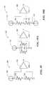
- magnetoresistance elements 284 , 286are shown in a series circuit 280 , in a parallel circuit 300 , and in an opposing circuit 320 .
- the circuits 280 and 300generate respective output signals 288 a , 308 a , which, like the normal mode configuration of Hall effect elements of FIG. 5 , are responsive to an external magnetic field, but not responsive to a diagnostic magnetic field experienced by the magnetoresistance elements 284 , 286 in different directions.
- the circuit 320generates an output signal 330 a , which, like the diagnostic mode configuration of Hall effect elements of FIGS. 6 and 6A , is responsive to a diagnostic magnetic field experienced by the magnetoresistance elements 284 , 286 in different directions, but not responsive to an external magnetic field.
- Hall effect elements 104 , 106 of FIGS. 7 , 8 , 8 B, 8 D, and 8 Fcan be replaced by magnetoresistance elements but with modifications to or removal of the switching circuits 102 , 108 .
- the coils 124 , 126can be comprised of a conductor 344 disposed on top of or underneath two magnetoresistance elements 340 , 342 .
- Magnetic fields 344 a , 344 btend to be in opposite directions and parallel to surfaces of the magnetoresistance elements 340 , 342 .
- the two diagnostic coils 124 , 126 of FIGS. 7 , 8 , 8 B, 8 D, and 8 Fcan be comprised of coils 346 , 348 , each arranged to generate magnetic fields 346 a , 348 a in opposite directions parallel to a maximum response axis of the magnetoresistance elements 340 , 342 .
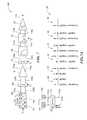
- FIGS. 12-12Dshow a variety of integrated circuit configurations. For clarity, only one magnetic field sensing element and one diagnostic coils (or conductor) are shown in the figures. However, one of ordinary skill in the art will understand how to fabricate an integrated circuit having two magnetic field sensing elements and two diagnostic coils. It will be appreciated that some of the magnetic field sensors of FIGS. 12-12D are shown to have electromagnetic shields. However, in other embodiments, the electromagnetic shields are omitted. Similarly, magnetic field sensors of FIGS. 12-12D shown without electromagnetic shields, can, in some other embodiments, have electromagnetic shields.
- a cross section of a portion of a magnetic field sensor 370is representative of one of the two Hall effect elements 104 , 106 and one of the diagnostic coils 124 , 126 of FIGS. 7 , 8 , 8 B, 8 D, and 8 F.
- the magnetic field sensor 370includes a magnetic field sensing element 392 supported by a substrate 382 having a surface 382 a .
- the magnetic field sensing element 392may be impregnated into or diffused into and below the surface 382 a of the substrate 382 , such as is known for manufacturing of Hall effect elements.
- the magnetic field sensing element 392can have a maximum response axis 396 generally perpendicular to the surface 382 a of the substrate 382 .
- the magnetic field sensor 370can include metal layers 384 , 386 , 388 separated by insulating layers 376 , 378 , 380 . Other metal and insulating layers (not shown) can be disposed between the insulating layer 376 and the metal layer 384 .
- An electromagnetic shield 372can be disposed over another insulating layer 374 .
- Sections 394 a - 394 care representative of a diagnostic coil, such as one of the diagnostic coils 124 , 126 of FIGS. 7 , 8 , 8 B, 8 D, and 8 F.
- the sections 394 a - 394 ccan form one continuous self-test conductor, here disposed on different ones of the metal layers 384 , 386 , 388 and coupled by way of vias 390 a , 390 b .
- a self-test current carried by the self-test conductor 394 a - 394 ctends to form a self-test magnetic field along the maximum response axis 396 .
- a magnetic field sensor 400can include all of the layers of the magnetic field sensor 370 of FIG. 12 and also the magnetic field sensing element 392 of FIG. 12 , but the self-test conductor 394 a - 394 c of FIG. 12 can be replaced by a continuous external coil self-test conductor 402 , which, in some embodiments, can be disposed upon a circuit board 404 .
- the external self-test conductor 402is representative of one of the diagnostic coils 124 , 126 of FIGS. 7 , 8 , 8 B, 8 D, and 8 F.
- the self-test conductor 402shown on one metal layer of the circuit board 404 , can instead be formed from a plurality of metal layers upon the circuit board 404 .
- a self-test current carried by the self-test conductor 402tends to form a self-test magnetic field along the maximum response axis 396 .
- a magnetic field sensor 410can include all of the layers of the magnetic field sensors 370 of FIGS. 12 and 400 of FIG. 12A , but the external self-test conductor 402 of FIG. 12A can be replaced by a continuous external coil self-test conductor 414 . Furthermore, the magnetic field sensing element 392 of FIGS. 12 and 12A can be replaced by a magnetic field sensing element 412 having a maximum response axis 416 generally parallel to the surface 382 a of the substrate 382 (e.g., a magnetoresistance element).
- the external self-test conductor 414is representative of one of the diagnostic coils 124 , 126 of FIGS. 7 , 8 , 8 B, 8 D, and 8 F but for the magnetoresistance element arrangements of FIGS. 10-10B
- the magnetic field sensing element 412may be disposed on or near the surface 382 a of the substrate 382 , such as is known for manufacturing of magnetoresistance elements.
- the magnetic field sensing element 392can have a maximum response axis 416 generally parallel to the surface 382 a of the substrate 382 .
- a self-test current carried by the self-test conductor 414tends to form a self-test magnetic field along the maximum response axis 416 .
- a magnetic field sensor 420can include all of the layers of the magnetic field sensors 370 , 400 and 410 of FIGS. 12 , 12 A, and 12 B, respectively, and also the magnetic field sensing element 412 of FIG. 12B , but the external self-test conductor 414 of FIG. 12B can be replaced by an internal single conductor self-test conductor 422 as is apparent from FIG. 11 .
- the self-test conductor 422is representative of one of the diagnostic coils of FIGS. 7 , 8 , 8 B, 8 D, and 8 F.
- a plurality of self test conductorscan be used, which are arranged to provide a resulting magnetic field at the magnetic field sensing element 412 from the plurality of self test conductors generally aligned with the maximum response axis 416 .
- a self-test current carried by the self-test conductor 422tends to form a self-test magnetic field along the maximum response axis 416 .
- a magnetic field sensor 430can include all of the layers of the magnetic field sensors 370 , 400 , 410 , and 420 of FIGS. 12 , 12 A, 12 B, and 12 C, respectively, but the internal self-test conductor 422 of FIG. 12C can be replaced by an external single conductor self-test conductor 432 , which, in some embodiments, can be disposed upon a circuit board 434 .
- the self-test conductor 432is representative of one of the diagnostic coils of FIGS. 7 , 8 , 8 B, 8 D, and 8 F.
- While one self test conductor 432is shown, in other embodiments, a plurality of self test conductors can be used, which are arranged to provide a resulting magnetic field at the magnetic field sensing element 412 from the plurality of self test conductors generally aligned with the maximum response axis 416 .
- a self-test current carried by the self-test conductor 432tends to form a self-test magnetic field along the maximum response axis 416 .
- FIGS. 12-12Dshow various alternative embodiments associated with the magnetic field sensors of FIGS. 7 8 , 8 B, 8 D, and 8 F, it will be recognized that there are many other possible configurations, including, but not limited to, combinations of the configurations shown.
- FIGS. 12-12Dare representative of portions of magnetic field sensors 370 , 400 , 410 , 420 , 430 , it should be understood that the magnetic field sensing elements and the self-test current conductors can be disposed on the same substrate as other portions of the magnetic field sensors of FIGS. 7 , 8 , 8 B, 8 D, and 8 F, or, in other embodiments on a second different substrate from the other portions of the magnetic field sensors of FIGS. 7 , 8 , 8 B, 8 D, and 8 F.
- a magnetic field sensor 444here encased in a package 442 , can be the same as or similar to the magnetic field sensors of FIGS. 7 , 8 , 8 B, 8 D, and 8 F.
- the magnetic field sensor 444can be coupled to a lead frame having leads 446 .
- the leads 446can be electrically coupled to a circuit board 450 .
- the magnetic field sensor 444can be responsive to a magnetic field 448 perpendicular to a major surface of the magnetic field sensor 444 , such as may be generated by proximity of a magnetic field source 440 , for example, a ferromagnetic object.
- a magnetic field sensor 456here encased in a package 454 , can be the same as or similar to the magnetic field sensors of FIGS. 7 , 8 , 8 B, 8 D, and 8 F.
- the magnetic field sensor 456can be coupled to a lead frame having leads, of which leads 460 a , 460 b are representative.
- the leads, e.g., 460 a , 460 bcan be electrically coupled to a circuit board 466 .
- the magnetic field sensor 456can be responsive to a magnetic field 464 parallel to a major surface of the magnetic field sensor 456 , such as may be generated by proximity of a magnetic field (or flux) source 452 , for example, a ferromagnetic object.
- the leadscan be coupled with a measured conductor 458 , which can be formed as a part of the lead frame of which the leads 460 a , 460 b are another part.
- a measured current carried by the measured conductor 458tends to form a magnetic field 462 going into or out of the page, depending upon a direction of the current carried by the measured conductor 458 .
- the magnetic field sensor 456can be a current sensor and the magnetic field sensor 456 can instead be responsive to the magnetic field 462 perpendicular to the major surface of the magnetic field sensor 456 (i.e., to the current) rather than to the magnetic field 464 .
- the magnetic field sensor 456can be disposed having a major surface parallel to the circuit board 466 .
- a magnetic field sensor 470here encased in a package 468 , can be the same as or similar to the magnetic field sensors of FIGS. 7 , 8 , 8 B, 8 D, and 8 F.
- the magnetic field sensor 470can be coupled to a lead frame having leads, of which a lead 474 is representative.
- the leads, e.g., 474can be electrically coupled to a circuit board 476 .
- the magnetic field sensor 470can be responsive to a magnetic field generated by proximity of a magnetic field source 472 within the package 468 .
- the magnetic field source 472can be a measured current conductor similar to the measured current conductor 458 of FIG. 12F .
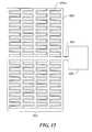
- an exemplary electromagnetic shield 800can be the same as or similar to the electromagnetic shield 372 of FIG. 12 .
- the electromagnetic shield 800is placed generally over a magnetic field sensing element 816 , which can be the same as or similar to the magnetic field sensing element 392 of FIG. 12 .
- the electromagnetic shield 800includes a first portion 802 and a second portion 804 separated by a slit 806 .
- the first portion 802 and the second portion 804are coupled with a conductive region 808 .
- a bonding pad 810allows the electromagnetic shield 800 to be coupled to a DC voltage, for example, to a ground voltage.
- the electromagnetic shield 800can be formed from a metal layer during manufacture of a magnetic field sensor, for example, the magnetic field sensors of FIGS. 7 , 8 , 8 B, 8 D, and 8 F.
- the metal layercan be comprised of a variety of materials, for example, aluminum, copper, gold, titanium, tungsten, chromium, or nickel.
- a nickel layerwould need to be thin so as not to concentrate the magnetic flux too much away from a Hall plate, especially if the shield has slits or slots.
- an electromagnetic shieldis not the same as a magnetic shield.
- An electromagnetic shieldis intended to block electromagnetic fields.
- a magnetic shieldis intended to block magnetic fields.
- AC eddy currents 812 , 814can be induced in the electromagnetic shield 800 .
- the eddy currents 812 , 814form into closed loops as shown.
- the closed loop eddy currents 812 , 814tend to result in a smaller magnetic field in proximity to the electromagnetic shield 800 than the magnetic field that induced the eddy currents 812 , 814 . Therefore, if the electromagnetic shield 800 were placed near a magnetic field sensing element, for example, the magnetic field sensing element 392 of FIG.
- the magnetic field sensing element 392experiences a smaller magnetic field than it would otherwise experience, resulting in a less sensitive magnetic field sensor, which is generally undesirable. Furthermore, if the magnetic field associated with the eddy current is not uniform or symmetrical about the magnetic field sensing element 392 , the magnetic field sensing element 392 might also generate an undesirable offset voltage.
- the slit 806tends to reduce a size (i.e., a diameter or path length) of the closed loops in which the eddy currents 812 , 814 travel. It will be understood that the reduced size of the closed loops in which the eddy currents 812 , 814 travel results in smaller eddy currents 812 , 814 and a smaller local effect on the AC magnetic field that induced the eddy current. Therefore, the sensitivity of a magnetic field sensor on which the magnetic field sensing element 816 and the electromagnetic shield 800 are used is less affected by the smaller eddy currents.
- the shield 800in relation to the magnetic field sensing element 816 as shown, so that the slit 806 passes over the magnetic field sensing element 816 , it will be understood that the magnetic field associated with any one of the eddy currents 812 , 814 tends to form magnetic fields passing through the magnetic field sensing element 816 in two directions, canceling over at least a portion of the area of the magnetic field sensing element 816 .
- another exemplary electromagnetic shield 850can be the same as or similar to the electromagnetic shield 372 of FIG. 12 .
- the electromagnetic shield 850includes four portions 852 - 858 separated by four slits 860 - 866 .
- the four portions 852 - 858are coupled with a conductive region 876 .
- a bonding pad 878allows the electromagnetic shield 850 to be coupled to a DC voltage, for example, a ground voltage.
- eddy currents 868 - 874can be induced in the electromagnetic shield 850 . Due to the four slits 860 - 866 , it will be understood that a size (i.e., a diameter or a path length) of the closed loops eddy currents 866 - 874 tends to be smaller than the size of the closed loop eddy currents 812 , 814 of FIG. 11 .
- the reduced size of the closed loops in which the eddy currents 868 - 874 travelresults in smaller eddy currents 868 - 874 and a smaller local affect on the AC magnetic field that induced the eddy current than that which results from the shield 800 of FIG. 13 . Therefore, the sensitivity of a magnetic field sensor on which the magnetic field sensing element 880 and the electromagnetic shield 850 are used is less affected by the smaller eddy currents 868 - 874 than the sensitivity of a current sensor using the shield 800 of FIG. 13 .
- the shield 850in relation to the magnetic field sensing element 880 as shown, so that the slits 860 - 866 pass over the magnetic field sensing element 880 , it will be understood that the magnetic field associated with any one of the eddy currents 868 - 874 , tends to form magnetic fields passing through the magnetic field sensing element 880 in two directions, canceling over at least a portion of the area of the magnetic field sensing element 880 .
- the electromagnetic shield 900includes a shielding portion 902 having interdigitated members, of which member 902 a is but one example.
- the interdigitated membersare coupled though a conductor portion 904 to a bonding pad 906 , which allows the electromagnetic shield 900 to be coupled to a DC voltage, for example, a ground voltage.
- the electromagnetic shield 900is able to support eddy currents having a much smaller size (i.e., diameter of path length) than the electromagnetic shield 850 of FIG. 14 or the electromagnetic shield 800 of FIG. 13 . Therefore, the electromagnetic shield 900 tends to have an even smaller negative affect on sensitivity of a magnetic field sensor than that described above.
- an electromagnetic shield 950can be the same as or similar to the electromagnetic shield 372 of FIG. 12 .
- the electromagnetic shield 950includes a shielding portion 952 having a plurality of members, of which member 952 a is but one example.
- the membersare coupled though a conductor portion 954 to a bonding pad 956 , which allows the electromagnetic shield 950 to be coupled to a DC voltage, for example, a ground voltage.
- a DC voltagefor example, a ground voltage.
- the shield 372 of FIGS. 12 , 12 A, 12 C, and 12 Dcan also have no features to reduce eddy currents.
- switches S 1 -S 8can correspond to the switching circuit 102 of FIGS. 7 , 8 , 8 B, 8 D, and 8 F.
- the switches S 1 -S 4can switch a direction of applied current to the two Hall effect elements 104 , 106 , to provide a first signal modulation comparable to that provided by the switches 60 a - 60 d of FIG. 2 or 80 a - 80 d of FIG. 3 .
- the switches S 5 -S 8perform two functions: to connect the Hall effect elements 104 , 106 into the normal mode or diagnostic mode of operation by selecting certain ones of the input nodes to each switch S 5 -S 8 , and also, in some embodiments, to modulate (or demodulate) the signal from the two Hall effect elements 104 , 106 by switching between the certain ones of the input nodes to each switch S 5 -S 8 .
- Reconnection and switching of the switches S 5 -S 8is more fully described below in conjunction with FIG. 18 , and differs for each one of the four above-described diagnostic modes of operation.
- the connection into the normal mode or diagnostic mode of operation of the switches S 5 -S 8(as well as the operation of the switches S 1 -S 4 ) is represented above within the switching circuit 102 of FIGS. 7 , 8 , 8 B, 8 D, and 8 F.
- the modulation function of the switches S 5 -S 8is represented separately by the switching circuit 108 of FIGS. 7 , 8 , 8 B, 8 D, and 8 F.
- the two switching circuits 102 , 108can be one switching circuit as shown in FIG. 17 .
- the two functions described above in conjunction with switches S 5 -S 8can be performed by two separate sets of switches.
- Circuit 1000provides for the above-described normal mode configuration, the above-described four diagnostic mode configurations, and also allows for the clocking or non-clocking functions of the switching circuits 102 , 108 described above, i.e., for normal mode of operation and for the first, second, third, and fourth version diagnostic modes of operation.
- a differential output signal, V+, V ⁇ ,is representative of an output signal from the switching circuit 108 of FIG. 7 , 8 , 8 B, 8 D, or 8 F, which output signal is different for each of the magnetic field sensors of FIG. 7 , 8 , 8 B, 8 D, or 8 F.
- the different output signalsare determined according to switch positions and clocking of switches discussed below in conjunction with FIG. 18 .
- FIG. 18in which switches, S 1 -S 8 of FIG. 17 are designated, a chart is representative of switch positions for the normal mode of operation and for the first, second, third, and fourth version diagnostic modes of operation.
- a column labeled “state”is representative of how the switches are changed during two phases of a clock signal, for the clock signals having relative frequencies described above in conjunction with FIGS. 7-8G .
- circuitsshow switch positions ( FIG. 17 ) and relative clock frequencies for the two phases (i.e., for the two drive directions provide by the switching circuit 102 of FIG. 7 , when operating in the normal mode of operation.
- circuitsshow switch positions ( FIG. 17 ) and relative clock frequencies for the two phases (i.e., for the two drive directions provide by the switching circuits 102 of FIG. 7 ) of the circuit 100 of FIG. 7 , operating generally in a diagnostic mode of operation.
- circuitsshow switch positions ( FIG. 17 ) and relative clock frequencies for the two phases (i.e., for the two drive directions provide by the switching circuits 102 of FIG. 8 ) of the circuit 150 of FIG. 8 , operating in the first version diagnostic mode of operation.
- circuitsshow switch positions ( FIG. 17 ) and relative clock frequencies for the two phases (i.e., for the two drive directions provide by the switching circuits 102 of FIG. 8B ) of the circuit 200 of FIG. 8B , operating in the second version diagnostic mode of operation.
- circuitsshow switch positions ( FIG. 17 ) and relative clock frequencies for the two phases (i.e., for the two drive directions provide by the switching circuits 102 of FIG. 8D ) of the circuit 220 of FIG. 8D , operating in the third version diagnostic mode of operation.
- circuitsshow switch positions ( FIG. 17 ) and relative clock frequencies for the two phases (i.e., for the two drive directions provide by the switching circuits 102 of FIG. 8F ) of the circuit 240 of FIG. 8F , operating in the fourth version diagnostic mode of operation.
Landscapes
- Physics & Mathematics (AREA)
- General Physics & Mathematics (AREA)
- Condensed Matter Physics & Semiconductors (AREA)
- Measuring Magnetic Variables (AREA)
- Hall/Mr Elements (AREA)
Abstract
Description
Claims (23)
Priority Applications (2)
| Application Number | Priority Date | Filing Date | Title |
|---|---|---|---|
| US12/840,324US8542010B2 (en) | 2009-07-22 | 2010-07-21 | Circuits and methods for generating a diagnostic mode of operation in a magnetic field sensor |
| US13/969,702US8692546B2 (en) | 2009-07-22 | 2013-08-19 | Circuits and methods for generating a diagnostic mode of operation in a magnetic field sensor |
Applications Claiming Priority (2)
| Application Number | Priority Date | Filing Date | Title |
|---|---|---|---|
| US22762809P | 2009-07-22 | 2009-07-22 | |
| US12/840,324US8542010B2 (en) | 2009-07-22 | 2010-07-21 | Circuits and methods for generating a diagnostic mode of operation in a magnetic field sensor |
Related Child Applications (1)
| Application Number | Title | Priority Date | Filing Date |
|---|---|---|---|
| US13/969,702ContinuationUS8692546B2 (en) | 2009-07-22 | 2013-08-19 | Circuits and methods for generating a diagnostic mode of operation in a magnetic field sensor |
Publications (2)
| Publication Number | Publication Date |
|---|---|
| US20110018533A1 US20110018533A1 (en) | 2011-01-27 |
| US8542010B2true US8542010B2 (en) | 2013-09-24 |
Family
ID=42664764
Family Applications (2)
| Application Number | Title | Priority Date | Filing Date |
|---|---|---|---|
| US12/840,324Active2031-03-22US8542010B2 (en) | 2009-07-22 | 2010-07-21 | Circuits and methods for generating a diagnostic mode of operation in a magnetic field sensor |
| US13/969,702ActiveUS8692546B2 (en) | 2009-07-22 | 2013-08-19 | Circuits and methods for generating a diagnostic mode of operation in a magnetic field sensor |
Family Applications After (1)
| Application Number | Title | Priority Date | Filing Date |
|---|---|---|---|
| US13/969,702ActiveUS8692546B2 (en) | 2009-07-22 | 2013-08-19 | Circuits and methods for generating a diagnostic mode of operation in a magnetic field sensor |
Country Status (5)
| Country | Link |
|---|---|
| US (2) | US8542010B2 (en) |
| EP (2) | EP2634592B1 (en) |
| JP (1) | JP5620989B2 (en) |
| KR (1) | KR101673185B1 (en) |
| WO (1) | WO2011011479A1 (en) |
Cited By (73)
| Publication number | Priority date | Publication date | Assignee | Title |
|---|---|---|---|---|
| US20120176128A1 (en)* | 2011-01-11 | 2012-07-12 | Invensense, Inc. | Micromachined resonant magnetic field sensors |
| US8692546B2 (en)* | 2009-07-22 | 2014-04-08 | Allegro Microsystems, Llc | Circuits and methods for generating a diagnostic mode of operation in a magnetic field sensor |
| US8947081B2 (en) | 2011-01-11 | 2015-02-03 | Invensense, Inc. | Micromachined resonant magnetic field sensors |
| US20150276892A1 (en)* | 2014-03-27 | 2015-10-01 | Texas Instruments Incorporated | Systems and methods for operating a hall-effect sensor without an applied magnetic field |
| WO2016077065A1 (en) | 2014-11-14 | 2016-05-19 | Allegro Microsystems, Llc | Magnetic field sensor having calibration circuitry and techniques |
| US20160352263A1 (en)* | 2014-08-08 | 2016-12-01 | Johnson Electric S.A. | Magnetic sensor and an integrated circuit |
| US20160349083A1 (en)* | 2014-08-08 | 2016-12-01 | Johnson Electric S.A. | Magnetic sensor and an integrated circuit |
| US20160352265A1 (en)* | 2014-08-08 | 2016-12-01 | Johnson Electric S.A. | Magnetic sensor and an integrated circuit |
| US20170016965A1 (en)* | 2015-07-17 | 2017-01-19 | Allegro Microsystems, Llc | Methods and Apparatus For Trimming A Magnetic Field Sensor |
| US9551762B1 (en) | 2015-07-29 | 2017-01-24 | Allegro Microsystems, Llc | Circuits and methods for removing a gain offset in a magnetic field sensor |
| US9645220B2 (en) | 2014-04-17 | 2017-05-09 | Allegro Microsystems, Llc | Circuits and methods for self-calibrating or self-testing a magnetic field sensor using phase discrimination |
| US9664494B2 (en) | 2013-05-10 | 2017-05-30 | Allegro Microsystems, Llc | Magnetic field sensor with immunity to external magnetic influences |
| US9698742B2 (en) | 2015-10-06 | 2017-07-04 | Allegro Microsystems, Llc | Electronic amplifier with a feedback circuit that includes a transconductance amplifier |
| US9735773B2 (en) | 2014-04-29 | 2017-08-15 | Allegro Microsystems, Llc | Systems and methods for sensing current through a low-side field effect transistor |
| US9804249B2 (en) | 2014-11-14 | 2017-10-31 | Allegro Microsystems, Llc | Dual-path analog to digital converter |
| US9804222B2 (en) | 2014-11-14 | 2017-10-31 | Allegro Microsystems, Llc | Magnetic field sensor with shared path amplifier and analog-to-digital-converter |
| US9817083B2 (en) | 2012-07-05 | 2017-11-14 | Allegro Microsystems, Llc | Magnetic field sensors and associated methods for removing undesirable spectral components |
| US9910088B2 (en) | 2013-12-26 | 2018-03-06 | Allegro Microsystems, Llc | Methods and apparatus for sensor diagnostics including programmable self-test signals |
| US10132879B2 (en) | 2016-05-23 | 2018-11-20 | Allegro Microsystems, Llc | Gain equalization for multiple axis magnetic field sensing |
| US10290608B2 (en) | 2016-09-13 | 2019-05-14 | Allegro Microsystems, Llc | Signal isolator having bidirectional diagnostic signal exchange |
| US10310028B2 (en) | 2017-05-26 | 2019-06-04 | Allegro Microsystems, Llc | Coil actuated pressure sensor |
| US10324141B2 (en) | 2017-05-26 | 2019-06-18 | Allegro Microsystems, Llc | Packages for coil actuated position sensors |
| WO2017219037A3 (en)* | 2016-06-17 | 2019-08-15 | Texas Instruments Incorporated | High bandwidth hall sensor |
| US10444299B2 (en) | 2017-09-11 | 2019-10-15 | Allegro Microsystems, Llc | Magnetic field sensor's front end and associated mixed signal method for removing chopper's related ripple |
| US10466298B2 (en) | 2014-11-14 | 2019-11-05 | Allegro Microsystems, Llc | Magnetic field sensor with shared path amplifier and analog-to-digital-converter |
| US10481219B2 (en) | 2017-09-11 | 2019-11-19 | Allegro Microsystems, Llc | Magnetic field sensor with feedback loop for test signal processing |
| US10527703B2 (en) | 2015-12-16 | 2020-01-07 | Allegro Microsystems, Llc | Circuits and techniques for performing self-test diagnostics in a magnetic field sensor |
| US10613158B2 (en) | 2017-10-12 | 2020-04-07 | Allegro Microsystems, Llc | Efficient signal path diagnostics for safety devices |
| US10641842B2 (en) | 2017-05-26 | 2020-05-05 | Allegro Microsystems, Llc | Targets for coil actuated position sensors |
| US10656170B2 (en) | 2018-05-17 | 2020-05-19 | Allegro Microsystems, Llc | Magnetic field sensors and output signal formats for a magnetic field sensor |
| US10670672B2 (en) | 2013-07-19 | 2020-06-02 | Allegro Microsystems, Llc | Method and apparatus for magnetic sensor producing a changing magnetic field |
| US10746814B2 (en) | 2018-06-21 | 2020-08-18 | Allegro Microsystems, Llc | Diagnostic methods and apparatus for magnetic field sensors |
| US10746818B2 (en) | 2016-07-12 | 2020-08-18 | Allegro Microsystems, Llc | Systems and methods for reducing high order hall plate sensitivity temperature coefficients |
| US10761120B2 (en) | 2017-02-17 | 2020-09-01 | Allegro Microsystems, Llc | Current sensor system |
| US10823586B2 (en) | 2018-12-26 | 2020-11-03 | Allegro Microsystems, Llc | Magnetic field sensor having unequally spaced magnetic field sensing elements |
| US10837943B2 (en) | 2017-05-26 | 2020-11-17 | Allegro Microsystems, Llc | Magnetic field sensor with error calculation |
| US10866117B2 (en) | 2018-03-01 | 2020-12-15 | Allegro Microsystems, Llc | Magnetic field influence during rotation movement of magnetic target |
| US10884031B2 (en) | 2018-08-17 | 2021-01-05 | Allegro Microsystems, Llc | Current sensor system |
| US10917092B2 (en) | 2018-04-06 | 2021-02-09 | Allegro Microsystems, Llc | Magnetic field sensor with switching network |
| US10955306B2 (en) | 2019-04-22 | 2021-03-23 | Allegro Microsystems, Llc | Coil actuated pressure sensor and deformable substrate |
| US10996289B2 (en) | 2017-05-26 | 2021-05-04 | Allegro Microsystems, Llc | Coil actuated position sensor with reflected magnetic field |
| US11047933B2 (en) | 2019-04-02 | 2021-06-29 | Allegro Microsystems, Llc | Fast response magnetic field sensors and associated methods for removing undesirable spectral components |
| US11047887B2 (en)* | 2018-08-31 | 2021-06-29 | Asahi Kasei Microdevices Corporation | Current sensor, detection device, detection method, and program |
| US11061084B2 (en) | 2019-03-07 | 2021-07-13 | Allegro Microsystems, Llc | Coil actuated pressure sensor and deflectable substrate |
| US11115244B2 (en) | 2019-09-17 | 2021-09-07 | Allegro Microsystems, Llc | Signal isolator with three state data transmission |
| US11163019B1 (en) | 2020-08-05 | 2021-11-02 | Allegro Microsystems, Llc | Magnetic field sensors having stray field rejection |
| US11169223B2 (en) | 2020-03-23 | 2021-11-09 | Allegro Microsystems, Llc | Hall element signal calibrating in angle sensor |
| US11194004B2 (en) | 2020-02-12 | 2021-12-07 | Allegro Microsystems, Llc | Diagnostic circuits and methods for sensor test circuits |
| US11226382B2 (en) | 2020-04-07 | 2022-01-18 | Allegro Microsystems, Llc | Current sensor system |
| US11237020B2 (en) | 2019-11-14 | 2022-02-01 | Allegro Microsystems, Llc | Magnetic field sensor having two rows of magnetic field sensing elements for measuring an angle of rotation of a magnet |
| US11262422B2 (en) | 2020-05-08 | 2022-03-01 | Allegro Microsystems, Llc | Stray-field-immune coil-activated position sensor |
| US20220082608A1 (en)* | 2017-12-29 | 2022-03-17 | Texas Instruments Incorporated | Direct current measurement of 1/f transistor noise |
| US11280637B2 (en) | 2019-11-14 | 2022-03-22 | Allegro Microsystems, Llc | High performance magnetic angle sensor |
| US11402280B2 (en)* | 2019-08-12 | 2022-08-02 | Allegro Microsystems, Llc | Magnetic sensor with improved stress compensation accounting for temperature |
| US11428755B2 (en) | 2017-05-26 | 2022-08-30 | Allegro Microsystems, Llc | Coil actuated sensor with sensitivity detection |
| US11493361B2 (en) | 2021-02-26 | 2022-11-08 | Allegro Microsystems, Llc | Stray field immune coil-activated sensor |
| US11555872B2 (en) | 2021-01-04 | 2023-01-17 | Allegro Microsystems, Llc | Reducing stray magnetic-field effects using a magnetic-field closed-loop system |
| US11561257B2 (en) | 2020-12-22 | 2023-01-24 | Allegro Microsystems, Llc | Signal path monitor |
| US11567108B2 (en) | 2021-03-31 | 2023-01-31 | Allegro Microsystems, Llc | Multi-gain channels for multi-range sensor |
| US11578997B1 (en) | 2021-08-24 | 2023-02-14 | Allegro Microsystems, Llc | Angle sensor using eddy currents |
| US11630130B2 (en) | 2021-03-31 | 2023-04-18 | Allegro Microsystems, Llc | Channel sensitivity matching |
| US11630169B1 (en) | 2022-01-17 | 2023-04-18 | Allegro Microsystems, Llc | Fabricating a coil above and below a magnetoresistance element |
| US11656250B2 (en) | 2021-09-07 | 2023-05-23 | Allegro Microsystems, Llc | Current sensor system |
| US11782105B2 (en) | 2022-01-17 | 2023-10-10 | Allegro Microsystems, Llc | Fabricating planarized coil layer in contact with magnetoresistance element |
| US11885866B2 (en) | 2022-05-31 | 2024-01-30 | Allegro Microsystems, Llc | Auto-calibration for coreless current sensors |
| US11892476B2 (en) | 2022-02-15 | 2024-02-06 | Allegro Microsystems, Llc | Current sensor package |
| US11927650B2 (en) | 2021-01-04 | 2024-03-12 | Allegro Microsystems, Llc | Magnetic-field closed-loop sensors with diagnostics |
| US11940470B2 (en) | 2022-05-31 | 2024-03-26 | Allegro Microsystems, Llc | Current sensor system |
| US12112865B2 (en) | 2022-03-15 | 2024-10-08 | Allegro Microsystems, Llc | Multiple branch bus bar for coreless current sensing application |
| US12174275B2 (en) | 2021-01-04 | 2024-12-24 | Allegro Microsystems, Llc | Magnetic field closed loop sensors with offset reduction |
| US12235294B2 (en) | 2022-04-15 | 2025-02-25 | Allegro MicroSystem, LLC | Current sensor assemblies for low currents |
| US12253576B2 (en) | 2023-01-10 | 2025-03-18 | Allegro Microsystems, Llc | Self-calibrating magnetoresistance-based magnetic field sensors |
| US12352786B2 (en) | 2021-09-07 | 2025-07-08 | Allegro Microsystems, Llc | Current sensor system |
Families Citing this family (62)
| Publication number | Priority date | Publication date | Assignee | Title |
|---|---|---|---|---|
| US9823090B2 (en) | 2014-10-31 | 2017-11-21 | Allegro Microsystems, Llc | Magnetic field sensor for sensing a movement of a target object |
| US8624588B2 (en)* | 2008-07-31 | 2014-01-07 | Allegro Microsystems, Llc | Apparatus and method for providing an output signal indicative of a speed of rotation and a direction of rotation as a ferromagnetic object |
| WO2010096367A1 (en) | 2009-02-17 | 2010-08-26 | Allegro Microsystems, Inc. | Circuits and methods for generating a self-test of a magnetic field sensor |
| US8564285B2 (en)* | 2010-07-28 | 2013-10-22 | Allegro Microsystems, Llc | Magnetic field sensor with improved differentiation between a sensed magnetic field signal and a noise signal |
| KR20120116036A (en)* | 2011-04-12 | 2012-10-22 | 삼성전기주식회사 | Hall sensor deleting off-set |
| US8680846B2 (en)* | 2011-04-27 | 2014-03-25 | Allegro Microsystems, Llc | Circuits and methods for self-calibrating or self-testing a magnetic field sensor |
| US8890518B2 (en) | 2011-06-08 | 2014-11-18 | Allegro Microsystems, Llc | Arrangements for self-testing a circular vertical hall (CVH) sensing element and/or for self-testing a magnetic field sensor that uses a circular vertical hall (CVH) sensing element |
| DE102011088365A1 (en)* | 2011-12-13 | 2013-06-13 | Zf Friedrichshafen Ag | Sensor device, method for detecting a position of the magnetic element with respect to a sensor element and magnetic element for a sensor device |
| US9201122B2 (en)* | 2012-02-16 | 2015-12-01 | Allegro Microsystems, Llc | Circuits and methods using adjustable feedback for self-calibrating or self-testing a magnetic field sensor with an adjustable time constant |
| US9817078B2 (en)* | 2012-05-10 | 2017-11-14 | Allegro Microsystems Llc | Methods and apparatus for magnetic sensor having integrated coil |
| EP2841957B1 (en)* | 2012-06-18 | 2017-02-22 | Allegro Microsystems, LLC | Magnetic field sensors and related techniques that can provide self-test information |
| US9068859B2 (en) | 2012-06-18 | 2015-06-30 | Allegro Microsystems, Llc | Magnetic field sensors and related techniques provide a self-test by communicating selected analog or digital samples of a proximity signal |
| US8754640B2 (en)* | 2012-06-18 | 2014-06-17 | Allegro Microsystems, Llc | Magnetic field sensors and related techniques that can provide self-test information in a formatted output signal |
| US9222990B2 (en) | 2012-06-18 | 2015-12-29 | Allegro Microsystems, Llc | Magnetic field sensors and related techniques that can communicate at least one of three or more potential categories in which one or more characteristic values of a proximity signal responsive to a proximity of a sensed object are categorized |
| US8860404B2 (en) | 2012-06-18 | 2014-10-14 | Allegro Microsystems, Llc | Magnetic field sensors and related techniques that can provide a self-test using signals and related thresholds |
| US8907669B2 (en) | 2012-07-24 | 2014-12-09 | Allegro Microsystems, Llc | Circuits and techniques for adjusting a sensitivity of a closed-loop current sensor |
| US9310446B2 (en)* | 2012-10-18 | 2016-04-12 | Analog Devices, Inc. | Magnetic field direction detector |
| US9354123B2 (en)* | 2012-12-26 | 2016-05-31 | Allegro Microsystems, Llc | Systems and methods for processing temperature data or other signals |
| US9383425B2 (en) | 2012-12-28 | 2016-07-05 | Allegro Microsystems, Llc | Methods and apparatus for a current sensor having fault detection and self test functionality |
| US10725100B2 (en)* | 2013-03-15 | 2020-07-28 | Allegro Microsystems, Llc | Methods and apparatus for magnetic sensor having an externally accessible coil |
| JP6212922B2 (en)* | 2013-04-23 | 2017-10-18 | 株式会社リコー | Chopper amplifier |
| JP6003816B2 (en)* | 2013-06-10 | 2016-10-05 | 日立金属株式会社 | Torque sensor |
| US9377327B2 (en) | 2013-06-28 | 2016-06-28 | Analog Devices Global | Magnetic field direction sensor |
| US10495699B2 (en) | 2013-07-19 | 2019-12-03 | Allegro Microsystems, Llc | Methods and apparatus for magnetic sensor having an integrated coil or magnet to detect a non-ferromagnetic target |
| US9810519B2 (en) | 2013-07-19 | 2017-11-07 | Allegro Microsystems, Llc | Arrangements for magnetic field sensors that act as tooth detectors |
| US9547048B2 (en)* | 2014-01-14 | 2017-01-17 | Allegro Micosystems, LLC | Circuit and method for reducing an offset component of a plurality of vertical hall elements arranged in a circle |
| US9739846B2 (en) | 2014-10-03 | 2017-08-22 | Allegro Microsystems, Llc | Magnetic field sensors with self test |
| US10094890B2 (en) | 2014-10-09 | 2018-10-09 | Panasonic Intellectual Property Management Co., Ltd. | Magnetic sensor |
| US9719806B2 (en) | 2014-10-31 | 2017-08-01 | Allegro Microsystems, Llc | Magnetic field sensor for sensing a movement of a ferromagnetic target object |
| US10712403B2 (en) | 2014-10-31 | 2020-07-14 | Allegro Microsystems, Llc | Magnetic field sensor and electronic circuit that pass amplifier current through a magnetoresistance element |
| US9720054B2 (en) | 2014-10-31 | 2017-08-01 | Allegro Microsystems, Llc | Magnetic field sensor and electronic circuit that pass amplifier current through a magnetoresistance element |
| US9823092B2 (en) | 2014-10-31 | 2017-11-21 | Allegro Microsystems, Llc | Magnetic field sensor providing a movement detector |
| US9638764B2 (en) | 2015-04-08 | 2017-05-02 | Allegro Microsystems, Llc | Electronic circuit for driving a hall effect element with a current compensated for substrate stress |
| DE102015216262B4 (en) | 2015-08-26 | 2019-03-28 | Fraunhofer-Gesellschaft zur Förderung der angewandten Forschung e.V. | Method and device for determining the cross-sensitivity of magnetic field sensors |
| FR3047318B1 (en)* | 2016-01-29 | 2019-05-03 | Continental Automotive France | METHOD AND DEVICE FOR TESTING A DETECTION SENSOR FOR A MOTOR VEHICLE |
| US10495700B2 (en) | 2016-01-29 | 2019-12-03 | Allegro Microsystems, Llc | Method and system for providing information about a target object in a formatted output signal |
| US10107873B2 (en) | 2016-03-10 | 2018-10-23 | Allegro Microsystems, Llc | Electronic circuit for compensating a sensitivity drift of a hall effect element due to stress |
| DE112017001473T5 (en) | 2016-03-22 | 2018-12-06 | Panasonic Intellectual Property Management Co., Ltd. | Rotation detection device |
| US11187763B2 (en) | 2016-03-23 | 2021-11-30 | Analog Devices International Unlimited Company | Offset compensation for magnetic field detector |
| US10271467B2 (en)* | 2016-04-04 | 2019-04-23 | Prasad S. Joshi | Systems and methods for flux cancelation in electronic devices |
| DE102017108972A1 (en)* | 2016-04-29 | 2017-11-02 | Johnson Electric S.A. | Magnetic sensor integrated circuit, motor assembly and utility device |
| CN107340483B (en)* | 2016-04-29 | 2021-08-20 | 德昌电机(深圳)有限公司 | Magnetic sensor, magnetic sensor integrated circuit, motor assembly and application equipment |
| DE102017108974A1 (en)* | 2016-04-29 | 2017-11-02 | Johnson Electric S.A. | Magnetic sensor integrated circuit, motor assembly and utility device |
| CN107332394B (en)* | 2016-04-29 | 2020-08-04 | 德昌电机(深圳)有限公司 | Magnetic sensor, magnetic sensor integrated circuit, motor assembly and application equipment |
| WO2017201002A2 (en) | 2016-05-17 | 2017-11-23 | Allegro Microsystems, Llc | Magnetic field sensors and output signal formats for a magnetic field sensor |
| US10041810B2 (en) | 2016-06-08 | 2018-08-07 | Allegro Microsystems, Llc | Arrangements for magnetic field sensors that act as movement detectors |
| US10012518B2 (en) | 2016-06-08 | 2018-07-03 | Allegro Microsystems, Llc | Magnetic field sensor for sensing a proximity of an object |
| US10260905B2 (en) | 2016-06-08 | 2019-04-16 | Allegro Microsystems, Llc | Arrangements for magnetic field sensors to cancel offset variations |
| JPWO2018012272A1 (en) | 2016-07-12 | 2019-05-09 | パナソニックIpマネジメント株式会社 | Magnetic sensor and detection device using the same |
| EP3578999B1 (en)* | 2017-02-02 | 2022-11-30 | Alps Alpine Co., Ltd. | Balance-type electric current sensor |
| JP6743770B2 (en)* | 2017-06-16 | 2020-08-19 | 株式会社デンソー | Position sensor |
| IT201700071213A1 (en) | 2017-06-26 | 2018-12-26 | St Microelectronics Srl | READING CIRCUIT FOR HALL SENSORS, CORRESPONDENT DEVICE AND PROCEDURE |
| CN107305241B (en)* | 2017-06-26 | 2021-01-29 | 新纳传感系统有限公司 | Magnetic sensing device and real-time self-checking method thereof |
| US10739165B2 (en) | 2017-07-05 | 2020-08-11 | Analog Devices Global | Magnetic field sensor |
| US10520559B2 (en) | 2017-08-14 | 2019-12-31 | Allegro Microsystems, Llc | Arrangements for Hall effect elements and vertical epi resistors upon a substrate |
| US10866289B2 (en)* | 2018-03-27 | 2020-12-15 | Allegro Microsystems, Llc | Magnetic field sensor and associated methods including differential chopping |
| US10955493B2 (en) | 2018-05-02 | 2021-03-23 | Analog Devices Global Unlimited Company | Magnetic sensor systems |
| US11255700B2 (en) | 2018-08-06 | 2022-02-22 | Allegro Microsystems, Llc | Magnetic field sensor |
| DE102020110682A1 (en)* | 2020-04-20 | 2021-10-21 | Infineon Technologies Ag | Magnetic field sensor apparatus and method |
| US11519941B2 (en) | 2020-07-27 | 2022-12-06 | Analog Devices International Unlimited Company | Current sensing device having an integrated electrical shield |
| US11802922B2 (en) | 2021-01-13 | 2023-10-31 | Allegro Microsystems, Llc | Circuit for reducing an offset component of a plurality of vertical hall elements arranged in one or more circles |
| WO2022161631A1 (en)* | 2021-01-29 | 2022-08-04 | Advantest Corporation | An integrated circuit, an apparatus for testing an integrated circuit, a method for testing an integrated circuit and a computer program for implementing this method using magnetic field |
Citations (74)
| Publication number | Priority date | Publication date | Assignee | Title |
|---|---|---|---|---|
| US4236832A (en) | 1977-06-29 | 1980-12-02 | Tokyo Shibaura Denki Kabushiki Kaisha | Strain insensitive integrated circuit resistor pair |
| US4438347A (en) | 1980-08-13 | 1984-03-20 | Siemens Aktiengesellschaft | Device for changing the electrical circuit configuration of integrated semiconductor circuits |
| JPS6148777A (en) | 1984-08-16 | 1986-03-10 | エルゲーツエツト・ランデイス・ウント・ギール・ツーク・アクチエンゲゼルシヤフト | Compensator for variation of conversion coefficient of magnetic field sensor |
| US4758943A (en) | 1985-04-03 | 1988-07-19 | Hightech Network Ab | Method and an apparatus for automatically tuning a process regulator |
| US4760285A (en) | 1987-03-30 | 1988-07-26 | Honeywell Inc. | Hall effect device with epitaxal layer resistive means for providing temperature independent sensitivity |
| EP0289414A2 (en) | 1987-04-28 | 1988-11-02 | Commissariat A L'energie Atomique | Method and device for the digitization and linearization of a quasi-sinusoidal sensor |
| US4823075A (en) | 1987-10-13 | 1989-04-18 | General Electric Company | Current sensor using hall-effect device with feedback |
| US4833406A (en) | 1986-04-17 | 1989-05-23 | Household Commercial Financial Services Inc. | Temperature compensated Hall-effect sensor apparatus |
| EP0338122A1 (en) | 1988-04-21 | 1989-10-25 | Landis & Gyr Business Support AG | Integrated circuit comprising a semiconductor magnetic field sensor |
| EP0357013A2 (en) | 1988-09-02 | 1990-03-07 | Honeywell Inc. | Magnetic field measuring circuit |
| US5247278A (en) | 1991-11-26 | 1993-09-21 | Honeywell Inc. | Magnetic field sensing device |
| US5329416A (en) | 1993-07-06 | 1994-07-12 | Alliedsignal Inc. | Active broadband magnetic flux rate feedback sensing arrangement |
| US5343143A (en) | 1992-02-11 | 1994-08-30 | Landis & Gyr Metering, Inc. | Shielded current sensing device for a watthour meter |
| GB2276727A (en) | 1993-04-01 | 1994-10-05 | Rolls Royce & Ass | Magnetoresistive magnetometer |
| US5412255A (en) | 1991-05-07 | 1995-05-02 | Vdo Adolf Schindling Ag | Switch device suitable for use in automotive vehicles |
| US5424558A (en) | 1993-05-17 | 1995-06-13 | High Yield Technology, Inc. | Apparatus and a method for dynamically tuning a particle sensor in response to varying process conditions |
| US5469058A (en) | 1992-12-30 | 1995-11-21 | Dunnam; Curt | Feedback enhanced sensor, alternating magnetic field detector |
| WO1996002849A1 (en) | 1994-07-19 | 1996-02-01 | Honeywell Inc. | Temperature compensation circuit for a hall effect element |
| US5521501A (en) | 1993-06-09 | 1996-05-28 | Institut Fuer Mikrostrukturtechnologie Und Optoelektronik E.V. | Magnetic field sensor constructed from a remagnetization line and one magnetoresistive resistor or a plurality of magnetoresistive resistors |
| US5621319A (en) | 1995-12-08 | 1997-04-15 | Allegro Microsystems, Inc. | Chopped hall sensor with synchronously chopped sample-and-hold circuit |
| DE19539458A1 (en) | 1995-10-24 | 1997-04-30 | Bosch Gmbh Robert | Self-testing Hall sensor, e.g for vehicle steering angle monitor |
| US5640090A (en) | 1995-01-31 | 1997-06-17 | Mitsumi Electric Company, Ltd. | Sensor IC |
| US5844140A (en) | 1996-08-27 | 1998-12-01 | Seale; Joseph B. | Ultrasound beam alignment servo |
| US6011770A (en) | 1997-12-10 | 2000-01-04 | Texas Instrumental Incorporated | Method and apparatus for high-order bandpass filter with linearly adjustable bandwidth |
| US6351506B1 (en) | 1999-04-19 | 2002-02-26 | National Semiconductor Corporation | Switched capacitor filter circuit having reduced offsets and providing offset compensation when used in a closed feedback loop |
| US6392478B1 (en) | 1999-11-23 | 2002-05-21 | U.S. Philips Corporation | Amplification device having an adjustable bandwidth |
| US20020084923A1 (en) | 2000-12-29 | 2002-07-04 | Jin Li | Method and apparatus for adaptive DC level control |
| US6437558B2 (en) | 1998-07-31 | 2002-08-20 | Spinix Corporation | Passive solid-state magnetic field sensors and applications therefor |
| US6436748B1 (en) | 1999-08-31 | 2002-08-20 | Micron Technology, Inc. | Method for fabricating CMOS transistors having matching characteristics and apparatus formed thereby |
| US20030038675A1 (en) | 2001-08-20 | 2003-02-27 | Gailus Paul H. | Feedback loop with adjustable bandwidth |
| US20030102909A1 (en) | 2000-07-05 | 2003-06-05 | Mario Motz | Amplifier circuit with offset compensation |
| JP2004177228A (en) | 2002-11-26 | 2004-06-24 | Matsushita Electric Works Ltd | Current measuring device |
| WO2004072672A1 (en) | 2003-02-11 | 2004-08-26 | Allegro Microsystems, Inc. | Integrated sensor |
| US6853178B2 (en) | 2000-06-19 | 2005-02-08 | Texas Instruments Incorporated | Integrated circuit leadframes patterned for measuring the accurate amplitude of changing currents |
| US6896407B2 (en) | 2001-11-05 | 2005-05-24 | Yamatake Corporation | Temperature information detecting device for angle sensor and position detecting device |
| US6917321B1 (en) | 2000-05-21 | 2005-07-12 | Analog Devices, Inc. | Method and apparatus for use in switched capacitor systems |
| EP1637898A1 (en) | 2004-09-16 | 2006-03-22 | Liaisons Electroniques-Mecaniques Lem S.A. | Continuously calibrated magnetic field sensor |
| US7038448B2 (en) | 2001-05-25 | 2006-05-02 | Sentron Ag | Magnetic field sensor |
| JP2006123012A (en) | 2004-10-26 | 2006-05-18 | Matsushita Electric Ind Co Ltd | Robot control method |
| EP1679524A1 (en) | 2005-01-11 | 2006-07-12 | Ecole Polytechnique Federale De Lausanne Epfl - Sti - Imm - Lmis3 | Hall sensor and method of operating a Hall sensor |
| US20060202692A1 (en) | 2005-02-23 | 2006-09-14 | Infineon Technologies Ag. | Magnetoresistive sensor element and concept for manufacturing and testing the same |
| US20070110199A1 (en) | 2005-11-15 | 2007-05-17 | Afshin Momtaz | Receive equalizer with adaptive loops |
| EP1850143A1 (en) | 2005-02-08 | 2007-10-31 | Rohm Co., Ltd. | Magnetic sensor circuit and portable terminal provided with such magnetic sensor circuit |
| US7292095B2 (en) | 2006-01-26 | 2007-11-06 | Texas Instruments Incorporated | Notch filter for ripple reduction in chopper stabilized amplifiers |
| WO2007138508A1 (en) | 2006-05-30 | 2007-12-06 | Koninklijke Philips Electronics N. V. | Sensor device with adaptive field compensation |
| US20070285089A1 (en)* | 2006-03-31 | 2007-12-13 | Daihen Corporation | Current detection printed board, voltage detection printed board, current/voltage detection printed board, current/voltage detector, current detector and voltage detector |
| US7319319B2 (en) | 2001-10-30 | 2008-01-15 | Tt Electronics Technology Limited | Sensing apparatus and method |
| US7325175B2 (en) | 2005-05-04 | 2008-01-29 | Broadcom Corporation | Phase adjust using relative error |
| DE102006037226A1 (en) | 2006-08-09 | 2008-02-14 | Fraunhofer-Gesellschaft zur Förderung der angewandten Forschung e.V. | Calibratable magnetic 3D-point sensor during measuring operation |
| US20080094055A1 (en) | 2006-10-19 | 2008-04-24 | Gerardo Monreal | Chopped hall effect sensor |
| US20080137784A1 (en) | 2006-12-08 | 2008-06-12 | Krone Andrew W | Reducing noise during a gain change |
| US20080238410A1 (en) | 2006-10-16 | 2008-10-02 | Ami Semiconductor Belgium Bvba | Auto-calibration of magnetic sensor |
| US20090001972A1 (en) | 2007-06-26 | 2009-01-01 | Devon Fernandez | Calibration circuits and methods for proximity detector |
| US20090001964A1 (en) | 2007-06-29 | 2009-01-01 | Bernhard Strzalkowski | Integrated Hybrid Current Sensor |
| US7474093B2 (en) | 2006-09-25 | 2009-01-06 | Infineon Technologies Ag | Magnetic field sensor apparatus |
| US20090085706A1 (en) | 2007-09-28 | 2009-04-02 | Access Business Group International Llc | Printed circuit board coil |
| DE102007041230B3 (en) | 2007-08-31 | 2009-04-09 | Fraunhofer-Gesellschaft zur Förderung der angewandten Forschung e.V. | Calibratable multi-dimensional magnetic point sensor and corresponding method and computer program therefor |
| WO2009108422A2 (en) | 2008-02-26 | 2009-09-03 | Allegro Microsystems, Inc. | Magnetic field sensor with automatic sensitivity adjustment |
| US7605647B1 (en) | 2008-04-29 | 2009-10-20 | Allegro Microsystems, Inc. | Chopper-stabilized amplifier and magnetic field sensor |
| US7635993B2 (en) | 2004-05-18 | 2009-12-22 | Nxp B.V. | Digital magnetic current sensor and logic |
| US7694200B2 (en) | 2007-07-18 | 2010-04-06 | Allegro Microsystems, Inc. | Integrated circuit having built-in self-test features |
| US7764118B2 (en) | 2008-09-11 | 2010-07-27 | Analog Devices, Inc. | Auto-correction feedback loop for offset and ripple suppression in a chopper-stabilized amplifier |
| US7769110B2 (en) | 2005-05-13 | 2010-08-03 | Broadcom Corporation | Threshold adjust system and method |
| US20100211347A1 (en) | 2009-02-17 | 2010-08-19 | Allegro Microsystems, Inc. | Circuits and Methods for Generating a Self-Test of a Magnetic Field Sensor |
| US7800389B2 (en) | 2007-07-13 | 2010-09-21 | Allegro Microsystems, Inc. | Integrated circuit having built-in self-test features |
| WO2011011479A1 (en) | 2009-07-22 | 2011-01-27 | Allegro Microsystems, Inc. | Circuits and methods for generating a diagnostic mode of operation in a magnetic field sensor |
| US20110048102A1 (en) | 2009-08-27 | 2011-03-03 | Devon Fernandez | Circuits and Methods for Calibration of a Motion Detector |
| JP2011052036A (en) | 2009-08-31 | 2011-03-17 | Nippon Synthetic Chem Ind Co Ltd:The | Curing agent for epoxy resin |
| US7936144B2 (en) | 2008-03-06 | 2011-05-03 | Allegro Microsystems, Inc. | Self-calibration algorithms in a small motor driver IC with an integrated position sensor |
| US7961823B2 (en) | 2004-06-02 | 2011-06-14 | Broadcom Corporation | System and method for adjusting multiple control loops using common criteria |
| US7990209B2 (en) | 2009-06-19 | 2011-08-02 | Allegro Microsystems, Inc. | Switched capacitor notch filter |
| US20110298448A1 (en) | 2010-06-03 | 2011-12-08 | Allegro Microsystems, Inc. | Motion Sensor, Method, and Computer-Readable Storage Medium Providing a Motion Sensor That Can Rapidly Calibrate Gains |
| US8128549B2 (en) | 2007-02-20 | 2012-03-06 | Neuronetics, Inc. | Capacitor failure detection |
| US20130093412A1 (en) | 2010-06-30 | 2013-04-18 | Lem Intellectual Property Sa | Autonomously calibrated magnetic field sensor |
Family Cites Families (10)
| Publication number | Priority date | Publication date | Assignee | Title |
|---|---|---|---|---|
| JPH03176682A (en)* | 1989-12-06 | 1991-07-31 | Hitachi Ltd | Magnetic field measurement device |
| JPH03248611A (en) | 1990-02-27 | 1991-11-06 | Mitsubishi Electric Corp | Temperature compensation gain setting controller |
| DE19606826A1 (en) | 1996-02-23 | 1997-08-28 | Knorr Bremse Electronic Gmbh | Method and device for checking a sensor |
| CN100443913C (en) | 2002-11-13 | 2008-12-17 | 松下电器产业株式会社 | Magnetic field sensor, magnetic field detection device, and magnetic field detection method |
| US20060219436A1 (en)* | 2003-08-26 | 2006-10-05 | Taylor William P | Current sensor |
| JP2006024845A (en) | 2004-07-09 | 2006-01-26 | Yamaha Corp | Probe card and inspecting method for magnetic sensor |
| JP2006126012A (en)* | 2004-10-28 | 2006-05-18 | Asahi Kasei Microsystems Kk | Magneto-electric conversion system, magneto-electric conversion apparatus and its control circuit |
| CN200986484Y (en) | 2006-11-28 | 2007-12-05 | 李彩珍 | Magnetic field sensor |
| EP2131205B1 (en)* | 2007-03-23 | 2018-05-02 | Asahi Kasei EMD Corporation | Magnetic sensor and its sensitivity measuring method |
| US7746675B2 (en)* | 2007-03-26 | 2010-06-29 | Virginia Tech Intellectual Properties, Inc. | Asymmetrical interleaving strategy for multi-channel power converters |
- 2010
- 2010-07-21KRKR1020127004427Apatent/KR101673185B1/enactiveActive
- 2010-07-21EPEP13169661.9Apatent/EP2634592B1/enactiveActive
- 2010-07-21USUS12/840,324patent/US8542010B2/enactiveActive
- 2010-07-21JPJP2012521746Apatent/JP5620989B2/enactiveActive
- 2010-07-21EPEP10739429.8Apatent/EP2446287B1/enactiveActive
- 2010-07-21WOPCT/US2010/042694patent/WO2011011479A1/enactiveApplication Filing
- 2013
- 2013-08-19USUS13/969,702patent/US8692546B2/enactiveActive
Patent Citations (96)
| Publication number | Priority date | Publication date | Assignee | Title |
|---|---|---|---|---|
| US4236832A (en) | 1977-06-29 | 1980-12-02 | Tokyo Shibaura Denki Kabushiki Kaisha | Strain insensitive integrated circuit resistor pair |
| US4438347A (en) | 1980-08-13 | 1984-03-20 | Siemens Aktiengesellschaft | Device for changing the electrical circuit configuration of integrated semiconductor circuits |
| JPS6148777A (en) | 1984-08-16 | 1986-03-10 | エルゲーツエツト・ランデイス・ウント・ギール・ツーク・アクチエンゲゼルシヤフト | Compensator for variation of conversion coefficient of magnetic field sensor |
| US4752733A (en) | 1984-08-16 | 1988-06-21 | Jan Petr | Compensating circuit for a magnetic field sensor |
| US4758943A (en) | 1985-04-03 | 1988-07-19 | Hightech Network Ab | Method and an apparatus for automatically tuning a process regulator |
| US4833406A (en) | 1986-04-17 | 1989-05-23 | Household Commercial Financial Services Inc. | Temperature compensated Hall-effect sensor apparatus |
| US4760285A (en) | 1987-03-30 | 1988-07-26 | Honeywell Inc. | Hall effect device with epitaxal layer resistive means for providing temperature independent sensitivity |
| EP0289414A2 (en) | 1987-04-28 | 1988-11-02 | Commissariat A L'energie Atomique | Method and device for the digitization and linearization of a quasi-sinusoidal sensor |
| EP0289414A3 (en) | 1987-04-28 | 1988-11-09 | Commissariat A L'energie Atomique | Method and device for the digitization and linearization of a quasi-sinusoidal sensor |
| US4823075A (en) | 1987-10-13 | 1989-04-18 | General Electric Company | Current sensor using hall-effect device with feedback |
| US4970411A (en) | 1988-04-21 | 1990-11-13 | Lgz Landis & Gyr Zug Ag | Arrangement for improving the longterm stability of a Hall element |
| EP0338122A1 (en) | 1988-04-21 | 1989-10-25 | Landis & Gyr Business Support AG | Integrated circuit comprising a semiconductor magnetic field sensor |
| EP0357013A3 (en) | 1988-09-02 | 1991-05-15 | Honeywell Inc. | Magnetic field measuring circuit |
| EP0357013A2 (en) | 1988-09-02 | 1990-03-07 | Honeywell Inc. | Magnetic field measuring circuit |
| US5412255A (en) | 1991-05-07 | 1995-05-02 | Vdo Adolf Schindling Ag | Switch device suitable for use in automotive vehicles |
| US5247278A (en) | 1991-11-26 | 1993-09-21 | Honeywell Inc. | Magnetic field sensing device |
| US5343143A (en) | 1992-02-11 | 1994-08-30 | Landis & Gyr Metering, Inc. | Shielded current sensing device for a watthour meter |
| US5469058A (en) | 1992-12-30 | 1995-11-21 | Dunnam; Curt | Feedback enhanced sensor, alternating magnetic field detector |
| GB2276727A (en) | 1993-04-01 | 1994-10-05 | Rolls Royce & Ass | Magnetoresistive magnetometer |
| US5424558A (en) | 1993-05-17 | 1995-06-13 | High Yield Technology, Inc. | Apparatus and a method for dynamically tuning a particle sensor in response to varying process conditions |
| US5521501A (en) | 1993-06-09 | 1996-05-28 | Institut Fuer Mikrostrukturtechnologie Und Optoelektronik E.V. | Magnetic field sensor constructed from a remagnetization line and one magnetoresistive resistor or a plurality of magnetoresistive resistors |
| US5329416A (en) | 1993-07-06 | 1994-07-12 | Alliedsignal Inc. | Active broadband magnetic flux rate feedback sensing arrangement |
| WO1996002849A1 (en) | 1994-07-19 | 1996-02-01 | Honeywell Inc. | Temperature compensation circuit for a hall effect element |
| US5640090A (en) | 1995-01-31 | 1997-06-17 | Mitsumi Electric Company, Ltd. | Sensor IC |
| DE19539458A1 (en) | 1995-10-24 | 1997-04-30 | Bosch Gmbh Robert | Self-testing Hall sensor, e.g for vehicle steering angle monitor |
| US5621319A (en) | 1995-12-08 | 1997-04-15 | Allegro Microsystems, Inc. | Chopped hall sensor with synchronously chopped sample-and-hold circuit |
| US5844140A (en) | 1996-08-27 | 1998-12-01 | Seale; Joseph B. | Ultrasound beam alignment servo |
| US6011770A (en) | 1997-12-10 | 2000-01-04 | Texas Instrumental Incorporated | Method and apparatus for high-order bandpass filter with linearly adjustable bandwidth |
| US6437558B2 (en) | 1998-07-31 | 2002-08-20 | Spinix Corporation | Passive solid-state magnetic field sensors and applications therefor |
| US6351506B1 (en) | 1999-04-19 | 2002-02-26 | National Semiconductor Corporation | Switched capacitor filter circuit having reduced offsets and providing offset compensation when used in a closed feedback loop |
| US6436748B1 (en) | 1999-08-31 | 2002-08-20 | Micron Technology, Inc. | Method for fabricating CMOS transistors having matching characteristics and apparatus formed thereby |
| US6392478B1 (en) | 1999-11-23 | 2002-05-21 | U.S. Philips Corporation | Amplification device having an adjustable bandwidth |
| US6917321B1 (en) | 2000-05-21 | 2005-07-12 | Analog Devices, Inc. | Method and apparatus for use in switched capacitor systems |
| US6853178B2 (en) | 2000-06-19 | 2005-02-08 | Texas Instruments Incorporated | Integrated circuit leadframes patterned for measuring the accurate amplitude of changing currents |
| US20030102909A1 (en) | 2000-07-05 | 2003-06-05 | Mario Motz | Amplifier circuit with offset compensation |
| US7190784B2 (en) | 2000-12-29 | 2007-03-13 | Legerity, Inc. | Method and apparatus for adaptive DC level control |
| US20020084923A1 (en) | 2000-12-29 | 2002-07-04 | Jin Li | Method and apparatus for adaptive DC level control |
| US7038448B2 (en) | 2001-05-25 | 2006-05-02 | Sentron Ag | Magnetic field sensor |
| US20030038675A1 (en) | 2001-08-20 | 2003-02-27 | Gailus Paul H. | Feedback loop with adjustable bandwidth |
| US7319319B2 (en) | 2001-10-30 | 2008-01-15 | Tt Electronics Technology Limited | Sensing apparatus and method |
| US6896407B2 (en) | 2001-11-05 | 2005-05-24 | Yamatake Corporation | Temperature information detecting device for angle sensor and position detecting device |
| JP2004177228A (en) | 2002-11-26 | 2004-06-24 | Matsushita Electric Works Ltd | Current measuring device |
| US7746056B2 (en) | 2003-02-11 | 2010-06-29 | Allegro Microsystems, Inc. | Integrated sensor |
| US7518354B2 (en) | 2003-02-11 | 2009-04-14 | Allegro Microsystems, Inc. | Multi-substrate integrated sensor |
| WO2004072672A1 (en) | 2003-02-11 | 2004-08-26 | Allegro Microsystems, Inc. | Integrated sensor |
| US7259545B2 (en) | 2003-02-11 | 2007-08-21 | Allegro Microsystems, Inc. | Integrated sensor |
| US7635993B2 (en) | 2004-05-18 | 2009-12-22 | Nxp B.V. | Digital magnetic current sensor and logic |
| US7961823B2 (en) | 2004-06-02 | 2011-06-14 | Broadcom Corporation | System and method for adjusting multiple control loops using common criteria |
| US20070247141A1 (en) | 2004-09-16 | 2007-10-25 | Liaisons Electroniques-Mecaniques Lem S.A. | Continuosly Calibrated Magnetic Field Sensor |
| JP2008513762A (en) | 2004-09-16 | 2008-05-01 | リエゾン、エレクトロニク−メカニク、エルウエム、ソシエテ、アノニム | Continuous calibration magnetic field sensor |
| US7746065B2 (en)* | 2004-09-16 | 2010-06-29 | Liaisons Electroniques-Mecaniques Lem S.A. | Continuously calibrated magnetic field sensor |
| WO2006056829A1 (en) | 2004-09-16 | 2006-06-01 | Liaisons Electroniques-Mécaniques LEM S.A. | Continuously calibrated magnetic field sensor |
| EP1637898A1 (en) | 2004-09-16 | 2006-03-22 | Liaisons Electroniques-Mecaniques Lem S.A. | Continuously calibrated magnetic field sensor |
| JP2006123012A (en) | 2004-10-26 | 2006-05-18 | Matsushita Electric Ind Co Ltd | Robot control method |
| EP1679524A1 (en) | 2005-01-11 | 2006-07-12 | Ecole Polytechnique Federale De Lausanne Epfl - Sti - Imm - Lmis3 | Hall sensor and method of operating a Hall sensor |
| EP1850143A1 (en) | 2005-02-08 | 2007-10-31 | Rohm Co., Ltd. | Magnetic sensor circuit and portable terminal provided with such magnetic sensor circuit |
| US7701208B2 (en)* | 2005-02-08 | 2010-04-20 | Rohm Co., Ltd. | Magnetic sensor circuit and portable terminal provided with such magnetic sensor circuit |
| US20060202692A1 (en) | 2005-02-23 | 2006-09-14 | Infineon Technologies Ag. | Magnetoresistive sensor element and concept for manufacturing and testing the same |
| US7323870B2 (en) | 2005-02-23 | 2008-01-29 | Infineon Technologies Ag | Magnetoresistive sensor element and method of assembling magnetic field sensor elements with on-wafer functional test |
| US7325175B2 (en) | 2005-05-04 | 2008-01-29 | Broadcom Corporation | Phase adjust using relative error |
| US7769110B2 (en) | 2005-05-13 | 2010-08-03 | Broadcom Corporation | Threshold adjust system and method |
| US20070110199A1 (en) | 2005-11-15 | 2007-05-17 | Afshin Momtaz | Receive equalizer with adaptive loops |
| US7292095B2 (en) | 2006-01-26 | 2007-11-06 | Texas Instruments Incorporated | Notch filter for ripple reduction in chopper stabilized amplifiers |
| US20070285089A1 (en)* | 2006-03-31 | 2007-12-13 | Daihen Corporation | Current detection printed board, voltage detection printed board, current/voltage detection printed board, current/voltage detector, current detector and voltage detector |
| WO2007138508A1 (en) | 2006-05-30 | 2007-12-06 | Koninklijke Philips Electronics N. V. | Sensor device with adaptive field compensation |
| DE102006037226A1 (en) | 2006-08-09 | 2008-02-14 | Fraunhofer-Gesellschaft zur Förderung der angewandten Forschung e.V. | Calibratable magnetic 3D-point sensor during measuring operation |
| US7474093B2 (en) | 2006-09-25 | 2009-01-06 | Infineon Technologies Ag | Magnetic field sensor apparatus |
| US20080238410A1 (en) | 2006-10-16 | 2008-10-02 | Ami Semiconductor Belgium Bvba | Auto-calibration of magnetic sensor |
| US8134358B2 (en)* | 2006-10-16 | 2012-03-13 | Semiconductor Components Industries, Llc | Method of auto calibrating a magnetic field sensor for drift and structure therefor |
| WO2008048379A1 (en) | 2006-10-19 | 2008-04-24 | Allegro Microsystems, Inc. | Chopped hall effect sensor |
| US7425821B2 (en) | 2006-10-19 | 2008-09-16 | Allegro Microsystems, Inc. | Chopped Hall effect sensor |
| US20080094055A1 (en) | 2006-10-19 | 2008-04-24 | Gerardo Monreal | Chopped hall effect sensor |
| US7729675B2 (en) | 2006-12-08 | 2010-06-01 | Silicon Laboratories Inc. | Reducing noise during a gain change |
| US20080137784A1 (en) | 2006-12-08 | 2008-06-12 | Krone Andrew W | Reducing noise during a gain change |
| US8128549B2 (en) | 2007-02-20 | 2012-03-06 | Neuronetics, Inc. | Capacitor failure detection |
| US20090001972A1 (en) | 2007-06-26 | 2009-01-01 | Devon Fernandez | Calibration circuits and methods for proximity detector |
| US20090001964A1 (en) | 2007-06-29 | 2009-01-01 | Bernhard Strzalkowski | Integrated Hybrid Current Sensor |
| US7800389B2 (en) | 2007-07-13 | 2010-09-21 | Allegro Microsystems, Inc. | Integrated circuit having built-in self-test features |
| US7694200B2 (en) | 2007-07-18 | 2010-04-06 | Allegro Microsystems, Inc. | Integrated circuit having built-in self-test features |
| DE102007041230B3 (en) | 2007-08-31 | 2009-04-09 | Fraunhofer-Gesellschaft zur Förderung der angewandten Forschung e.V. | Calibratable multi-dimensional magnetic point sensor and corresponding method and computer program therefor |
| US20090085706A1 (en) | 2007-09-28 | 2009-04-02 | Access Business Group International Llc | Printed circuit board coil |
| US7923996B2 (en) | 2008-02-26 | 2011-04-12 | Allegro Microsystems, Inc. | Magnetic field sensor with automatic sensitivity adjustment |
| US8030918B2 (en) | 2008-02-26 | 2011-10-04 | Allegro Microsystems, Inc. | Magnetic field sensor with automatic sensitivity adjustment |
| WO2009108422A3 (en) | 2008-02-26 | 2009-12-10 | Allegro Microsystems, Inc. | Magnetic field sensor with automatic sensitivity adjustment |
| WO2009108422A2 (en) | 2008-02-26 | 2009-09-03 | Allegro Microsystems, Inc. | Magnetic field sensor with automatic sensitivity adjustment |
| US7936144B2 (en) | 2008-03-06 | 2011-05-03 | Allegro Microsystems, Inc. | Self-calibration algorithms in a small motor driver IC with an integrated position sensor |
| US7605647B1 (en) | 2008-04-29 | 2009-10-20 | Allegro Microsystems, Inc. | Chopper-stabilized amplifier and magnetic field sensor |
| US7764118B2 (en) | 2008-09-11 | 2010-07-27 | Analog Devices, Inc. | Auto-correction feedback loop for offset and ripple suppression in a chopper-stabilized amplifier |
| WO2010096367A1 (en) | 2009-02-17 | 2010-08-26 | Allegro Microsystems, Inc. | Circuits and methods for generating a self-test of a magnetic field sensor |
| US20100211347A1 (en) | 2009-02-17 | 2010-08-19 | Allegro Microsystems, Inc. | Circuits and Methods for Generating a Self-Test of a Magnetic Field Sensor |
| US7990209B2 (en) | 2009-06-19 | 2011-08-02 | Allegro Microsystems, Inc. | Switched capacitor notch filter |
| WO2011011479A1 (en) | 2009-07-22 | 2011-01-27 | Allegro Microsystems, Inc. | Circuits and methods for generating a diagnostic mode of operation in a magnetic field sensor |
| US20110048102A1 (en) | 2009-08-27 | 2011-03-03 | Devon Fernandez | Circuits and Methods for Calibration of a Motion Detector |
| JP2011052036A (en) | 2009-08-31 | 2011-03-17 | Nippon Synthetic Chem Ind Co Ltd:The | Curing agent for epoxy resin |
| US20110298448A1 (en) | 2010-06-03 | 2011-12-08 | Allegro Microsystems, Inc. | Motion Sensor, Method, and Computer-Readable Storage Medium Providing a Motion Sensor That Can Rapidly Calibrate Gains |
| US20130093412A1 (en) | 2010-06-30 | 2013-04-18 | Lem Intellectual Property Sa | Autonomously calibrated magnetic field sensor |
Non-Patent Citations (92)
| Title |
|---|
| Ausserlechner et al.; "Compensation of the Piezo-Hall Effect in Integrated Hall Sensors on (100)-Si;" IEEE Sensors Journal, vol. 7, No. 11; Nov. 2007; ISBN: 1530-437X; pp. 1475-1482. |
| Ausserlechner et al.; "Drift of Magnetic Sensitivity of Small Hall Sensors Due to Moisture Absorbed by the IC-Package;" Proceedings of IEEE Sensors, 2004; vol. 1; Oct. 24, 2004; ISBN:0-7803-8692-2; pp. 455-458. |
| Ausserlechner; "Limits of Offset Cancellation by the Principle of Spinning Current Hall Probe;" Proceedings of IEEE Sensors; Oct. 2004; pp. 1117-1120. |
| Ausserlechner; "The piezo-Hall effect in n-silicon for arbitrary crystal orientation;" Proceedings of IEEE Sensors; vol. 3; Oct. 24, 2004; ISBN: 0-7803-8692-2; pp. 1149-1152. |
| Bahreyni, et al.; "A Resonant Micromachined Magnetic Field Sensor;" IEEE Sensors Journal; vol. 7, No. 9, Sep. 2007; pp. 1326-1334. |
| Barrettino, et al.; "CMOS-Based Monolithic Controllers for Smart Sensors Comprising Micromembranes and Microcantilevers;" IEEE Transactions on Circuits and Systems-I Regular Papers vol. 54, No. 1; Jan. 2007; pp. 141-152. |
| Baschirotto et al.; "Development and Analysis of PCB Vector 2-D Magnetic Field Sensor System for Electronic Compass;" IEEE Sensors Journal vol. 6, No. 2; Apr. 2006; pp. 365-371. |
| Bilotti et al.; "Monolithic Magnetic Hall Sensor Using Dynamic Quadrature Offset Cancellation;" IEEE Journal of Solid-State Circuits; vol. 32, Issue 6; Jun. 1997; pp. 829-836. |
| Blagojevic et al.; "FD SOI Hall Sensor Electronics Interfaces for Energy Measurement;" Microelectronics Journal 37; Sep. 2006; pp. 1576-1583. |
| Cesaretti et al.; "Circuits and Methods for Self-Calibrating or Self-Testing a Magnetic Field Sensor;" U.S. Appl. No. 13/095,371, filed Apr. 27, 2011; 62 pages. |
| Cessaretti et al; "Circuits and Methods Using Adjustable Feedback for Self-Calibrating or Self-Testing a Magnetic Field Sensor with an Adjustable Time Constraint;" U.S. Appl. No. 13/398,127; 85 pages. |
| Chinese Office Action dated Apr. 15, 2013; for CN Pat. App. No. 200980106535.4 4 pages. |
| Chinese Office Action dated Apr. 15, 2013; for CN Pat. App. No. 200980106565.4; 4 pages. |
| Chinese Response to Office Action; filed Jun. 27, 2013; for Chinese Pat. App. No. 200980106535.4; 12 pages. |
| Demierre, et al.; "Reference Magnetic Actuator for Self-Calibration of a Very Small Hall Sensor Array;" Sensors and Actuators A97-98; Apr. 2002; pp. 39-46. |
| EP Official Communication; dated Feb. 23, 2012; for EP. Pat. App. No. 10739429.8; 2 pages. |
| European Notice of Allowance; dated Jan. 4, 2013; for EP Pat. App. No. 10 739 429.8; 89 pages. |
| European Notice of Allowance; dated Jan. 4, 2013; for European Pat. App. No. 10 739 429.8; 7 pages. |
| European Response to Written Opinion; dated Sep. 4, 2012; for European Pat. App. No. 10739429.8; 11 pages. |
| European Search Report; dated Jul. 4, 2013; for EP Pat. App. No. 13169661.9; 11 pages. |
| Frick, et al.; "CMOS Microsystem for AC Current Measurement with Galvanic Isolation;" IEEE Sensors Journal; vol. 3, No. 6; Dec. 2003; pp. 752-760. |
| Halg; "Piezo-Hall Coefficients of n-Type Silicon;" Journal of Applied Physics; vol. 64, No. 1; Jul. 1, 1988; pp. 276-282. |
| Hosticka; "CMOS Sensor Systems;" Sensors and Actuators A66; Apr. 1998; pp. 335-341. |
| Japanese Notice of Reasons for Rejection (English translation); dated Apr. 4, 2013; for JP Pat. App. No. 2010-547666; 4 pages. |
| Kanda et al.; "The Piezo-Hall Effect in n-Silicon;" 22nd International Conference on the Physics of Semiconductors; vol. 1, Jan. 1995; pp. 89-92. |
| Kayal el al.; "Automatic Calibration of Hall Sensor Microsystems;" Microelectronics Journal 37; Sep. 2006; pp. 1569-1575. |
| Krammerer et al.: "A Hall effect sensors network insensitive to mechanical stress;" Proceedings of IEEE Sensors; vol. 3, Oct. 2004; pp. 1071-1074. |
| Letter from NTD Patent and Trademark Agency Ltd.; dated Jan. 19, 2013; enclosing Response to Official Action; for Chinese Pat. App. No. 200980106535.4; 14 pages. |
| Letter from NTD Patent and Trademark Agency; dated Jul. 11, 2013; for Chinese Pat. App. No. 200980106535.4; 1 page. |
| Letter from Yuasa & Hara; dated May 27, 2013; for JP Pat. App. No. 2010-547666; 2 pages. |
| Letter to NTD Patent and Trademark Agency Ltd.; dated Dec. 11, 2012; with instructions to file Response to Official Action; for Chinese Pat. App. No. 200980106535.4; 3 pages. |
| Letter to NTD Patent and Trademark Agency; dated Jun. 19, 2013; for Chinese Pat. App. No. 200980106535.4; 11 pages. |
| Mangnani et al.; "Mechanical Stress Measurement Electronics Based on Piezo-Resistive and Piezo-Hall Effects;" 9th International Conference on Electronics, Circuits and Systems 2002; vol. 1; SBN: 0-7803-7596-3; Dec. 2002; pp. 363-366. |
| Manic et al.; "Short and Long-Term Stability Problems of Hall Plates in Plastic Packages;" IEEE 38th Annual International Reliability Physics Symposium; Apr. 2000; pp. 225-230. |
| Manic; "Drift in Silicon Integrated Sensors and Circuits Due to the Thermo-Mechanical Stresses;" Lausanne, École Polytechnique Fédérale De Lausanne 2000; 176 pages. |
| Motz et al.; "An Integrated Magnetic Sensor with Two Continuous-Time DeltaSigma-Converters and Stress Compensation Capability;" IEEE International Solid-State Circuits Conference; Digest of Technical Papers; Feb. 6, 2006; ISBN: 1-4244-0079-1; pp. 1151-1160. |
| Motz et al.; "An Integrated Magnetic Sensor with Two Continuous-Time ΔΣ-Converters and Stress Compensation Capability;" IEEE International Solid-State Circuits Conference; Digest of Technical Papers; Feb. 6, 2006; ISBN: 1-4244-0079-1; pp. 1151-1160. |
| Motz, et al.; "A Chopped Hall Sensor with Small Jitter and Programmable "True Power-On" Function;" IEEE Journal of Solid-State Circuits; vol. 40, No. 7; Jul. 2005; pp. 1533-1540. |
| Motz, et al.; "An Integrated Hall Sensor Platform Design for Position, Angle and Current Sensing;" IEEE Sensors 2006; Exco, Daegu, Korea / Oct. 22-25, 2006; pp. 1008-1011. |
| Munter; "A Low-offset Spinning-current Hall Plate;" Sensors and Actuators A21-A23; 1990; pp. 742-746. |
| Munter; "Electronic Circuitry for a Smart Spinning-current Hall Plate with Low Offset;" Sensors and Actuators A; Jun. 1991;.pp. 747-751. |
| Office Action dated Jul. 6, 2012; for U.S. Appl. No. 12/706,318, filed Feb. 16, 2010; 24 pages. |
| Office Action dated Jul. 6, 2012; for U.S. Appl. No. 12/706,318; 29 pages. |
| Office Action dated Jun. 11, 2013; for U.S. Appl. No. 13/095,371; 31 pages. |
| Office Action dated Jun. 12, 2013; U.S. Appl. No. 13/743,451; 24 pages. |
| Partin et al.; "Temperature Stable Hall Effect Sensors;" IEEE Sensors Journal, vol. 6, No. 1; Feb. 2006; pp. 106-110. |
| Pastre, et al.; "A Hall Sensor Analog Front End for Current Measurement with Continuous Gain Calibration;" IEEE Sensors Journal; vol. 7, No. 5; May 2007; pp. 860-867. |
| Pastre, et al.; "A Hall Sensor-Based Current Measurement Microsystem With Continuous Gain Calibration;" Research in Microelectronics and Electronics, IEEE vol. 2; Jul. 25; 2005; ISBN: 0-7803-9345-7; pp. 95-98. |
| PCT International Preliminary Report on Patentability and Written Opinion mailed Sep. 10, 2010 for PCT/US2009/031776. |
| PCT International Preliminary Report on Patentability and Written Opinion of the ISA for PCT Pat. App. No. PCT/US2010/024256; dated Sep. 1, 2011; 9 pages. |
| PCT International Preliminary Report on Patentability and Written Opinion of the ISA; dated Feb. 2, 2012; for PCT Pat. App. No. PCT/US2010/042694; 11 sheets. |
| PCT Search Report and Written Opinion of the ISA for PCT Pat. App. No. PCT/US2012/032315; dated Jun. 22, 2012; 16 pages. |
| PCT Search Report and Written Opinion of the ISA for PCT/US2009/031776 dated Oct. 23, 2009. |
| PCT Search Report and Written Opinion of the ISA for PCT/US2010/024256 dated Aug. 11, 2010. |
| PCT Search Report and Written Opinion of the ISA for PCT/US2010/042694 dated Sep. 27, 2010. |
| PCT Search Report and Written Opinion; dated May 27, 2013; for PCT Pat. App. No. PCT/US2013/021143; 13 pages. |
| Popovic; "Sensor Microsystems;" Proc. 20th International Conference on Microelectronics (MWIL 95); vol. 2, NIS, Serbia, 12-14; Sep. 1995; pp. 531-537. |
| Randhawa; "Monolithic Integrated Hall Devices in Silicon Circuits;" Microelectronics Journal; vol. 12, No. 6; Sep. 14-17, 1981; pp. 24-29. |
| Response to European Written Opinion; filed on Sep. 4, 2012; for EP Pat. App. No. 10739429.8; 11 pages. |
| Ruther et al.; "Integrated CMOS-Based Sensor Array for Mechanical Stress Mapping;" 5th IEEE Conference on Sensors, Oct. 2007; pp. 1131-1134. |
| Ruther et al.; "Theromagnetic Residual Offset in Integrated Hall Plates;" IEEE Sensors Journal; vol. 3, No. 6; Dec. 2003; pp. 693-699. |
| Sargent; "Switched-capacitor IC controls feedback loop;" EDN; Design Ideas; Feb. 17, 2000; pp. 154 and 156. |
| Schneider, et al.; "Temperature Calibration of CMOS Magnetic Vector Probe for Contactless Angle Measurement System;" IEDM; Dec. 1996; pp. 533-536. |
| Schott et al.; "Linearizing Integrated Hall Devices;" 1997 International Conference on Solid-State Sensors and Actuators, Jun. 16-19, 1997; pp. 393-396. |
| Schott, et al.; "CMOS Single-Chip Electronic Compass with Microcontroller;" IEEE Journal of Solid-State Circuits; vol. 42, No. 12; Dec. 2007; pp. 2923-2933. |
| Simon et al.; "Autocalibration of Silicon Hall Devices;" 8th International Conference on Solid-State Sensors and Actuators; vol. 2; Jun. 25, 1995; pp. 237-240. |
| Steiner et al; Offset Reduction in Hall Devices by Continuous Spinning Current Method; Sensors and Actuators A66; 1998; pp. 167-172. |
| Steiner: "Double-Hall Sensor with Self-Compensated Offset;" Electron Devices Meeting; IDSM '97 Technical Digest; Dec. 7-10, 1997; pp. 911-914. |
| Stellrecht et al.; Characterization of Hygroscopic Swelling Behavior of Mold Compounds and Plastic Packages; IEEE Transactions on Components and Packaging Technologies; vol. 27, No. 3; Sep. 2004; pp. 499-506. |
| Tian et al.; "Multiple Sensors on Pulsed Eddy-Current Detection for 3-D Subsurface Crack Assessment;" IEEE Sensors Journal, vol. 5, No. 1; Feb. 2005; pp. 90-96. |
| Translated Chinese Office Action dated Apr. 15, 2013; for CN Pat. App. No. 200980106565.4; 5 pages. |
| Translation of Chinese Office Action; dated Apr. 15, 2013; for CN Pat. App. No. 200980106535.4 5 pages. |
| Trontelj et al; "CMOS Integrated Magnetic Field Source Used as a Reference in Magnetic Field Sensors on Common Substrate;" WEP 1-6; IMTC; May 1994; pp. 461-463. |
| U.S. Appl. No. 12/706,318, filed Feb. 16, 2010; Part 1 of 9; 350 pages. |
| U.S. Appl. No. 12/706,318, filed Feb. 16, 2010; Part 2 of 9; 350 pages. |
| U.S. Appl. No. 12/706,318, filed Feb. 16, 2010; Part 3 of 9; 350 pages. |
| U.S. Appl. No. 12/706,318, filed Feb. 16, 2010; Part 4 of 9; 200 pages. |
| U.S. Appl. No. 12/706,318, filed Feb. 16, 2010; Part 5 of 9; 150 pages. |
| U.S. Appl. No. 12/706,318, filed Feb. 16, 2010; Part 6 of 9; 350 pages. |
| U.S. Appl. No. 12/706,318, filed Feb. 16, 2010; Part 7 of 9; 200 pages. |
| U.S. Appl. No. 12/706,318, filed Feb. 16, 2010; Part 8 of 9; 150 pages. |
| U.S. Appl. No. 12/706,318, filed Feb. 16, 2010; Part 9 of 9; 350 pages. |
| U.S. Appl. No. 13/743,451, filed Jan. 17, 2013, Friedrich et al. |
| U.S. Notice of Allowance; dated Dec. 10, 2012; for U.S. Appl. No. 12/706,318; 9 pages. |
| U.S. Pat. No. 7,923,996; issued on Apr. 12, 2011; Part 1 of 5; 300 pages. |
| U.S. Pat. No. 7,923,996; issued on Apr. 12, 2011; Part 2 of 5; 300 pages. |
| U.S. Pat. No. 7,923,996; issued on Apr. 12, 2011; Part 3 of 5; 300 pages. |
| U.S. Pat. No. 7,923,996; issued on Apr. 12, 2011; Part 4 of 5; 300 pages. |
| U.S. Pat. No. 7,923,996; issued on Apr. 12, 2011; Part 5 of 5; 279 pages. |
| U.S. Pat. No. 8,030,918; issued on Oct. 4, 2011; 534pages. |
| Wu, et al.; "A Chopper Current-Feedback Instrumentation Amplifier with a 1mHz 1/f Noise Corner and an AC-Coupled Ripple-Reduction Loop;" IEEE International Solid-State Circuits Conference; Feb. 10, 2009; pp. 322-324. |
| Zou et al.; "Three-Dimensional Die Surface Stress Measurements in Delaminated and Non-Delaminated Plastic Packages;" 48th Electronic Components and Technology Conference; May 25, 1998; pp. 1223-1234. |
Cited By (97)
| Publication number | Priority date | Publication date | Assignee | Title |
|---|---|---|---|---|
| US8692546B2 (en)* | 2009-07-22 | 2014-04-08 | Allegro Microsystems, Llc | Circuits and methods for generating a diagnostic mode of operation in a magnetic field sensor |
| US8860409B2 (en)* | 2011-01-11 | 2014-10-14 | Invensense, Inc. | Micromachined resonant magnetic field sensors |
| US8947081B2 (en) | 2011-01-11 | 2015-02-03 | Invensense, Inc. | Micromachined resonant magnetic field sensors |
| US20120176128A1 (en)* | 2011-01-11 | 2012-07-12 | Invensense, Inc. | Micromachined resonant magnetic field sensors |
| US9817083B2 (en) | 2012-07-05 | 2017-11-14 | Allegro Microsystems, Llc | Magnetic field sensors and associated methods for removing undesirable spectral components |
| US9664494B2 (en) | 2013-05-10 | 2017-05-30 | Allegro Microsystems, Llc | Magnetic field sensor with immunity to external magnetic influences |
| US11313924B2 (en) | 2013-07-19 | 2022-04-26 | Allegro Microsystems, Llc | Method and apparatus for magnetic sensor producing a changing magnetic field |
| US12061246B2 (en) | 2013-07-19 | 2024-08-13 | Allegro Microsystems, Llc | Method and apparatus for magnetic sensor producing a changing magnetic field |
| US10670672B2 (en) | 2013-07-19 | 2020-06-02 | Allegro Microsystems, Llc | Method and apparatus for magnetic sensor producing a changing magnetic field |
| US10073136B2 (en) | 2013-12-26 | 2018-09-11 | Allegro Microsystems, Llc | Methods and apparatus for sensor diagnostics including sensing element operation |
| US10488458B2 (en) | 2013-12-26 | 2019-11-26 | Allegro Microsystems, Llc | Methods and apparatus for sensor diagnostics |
| US11313899B2 (en) | 2013-12-26 | 2022-04-26 | Allegro Microsystems, Llc | Methods and apparatus for sensor diagnostics |
| US9910088B2 (en) | 2013-12-26 | 2018-03-06 | Allegro Microsystems, Llc | Methods and apparatus for sensor diagnostics including programmable self-test signals |
| US20150276892A1 (en)* | 2014-03-27 | 2015-10-01 | Texas Instruments Incorporated | Systems and methods for operating a hall-effect sensor without an applied magnetic field |
| US9791521B2 (en)* | 2014-03-27 | 2017-10-17 | Texas Instruments Incorporated | Systems and methods for operating a hall-effect sensor without an applied magnetic field |
| US9645220B2 (en) | 2014-04-17 | 2017-05-09 | Allegro Microsystems, Llc | Circuits and methods for self-calibrating or self-testing a magnetic field sensor using phase discrimination |
| US9735773B2 (en) | 2014-04-29 | 2017-08-15 | Allegro Microsystems, Llc | Systems and methods for sensing current through a low-side field effect transistor |
| US20160349083A1 (en)* | 2014-08-08 | 2016-12-01 | Johnson Electric S.A. | Magnetic sensor and an integrated circuit |
| US9716453B2 (en)* | 2014-08-08 | 2017-07-25 | Johnson Electric S.A. | Magnetic sensor and an integrated circuit |
| US9696182B2 (en)* | 2014-08-08 | 2017-07-04 | Johnson Electric S.A. | Magnetic sensor and an integrated circuit |
| US9692329B2 (en)* | 2014-08-08 | 2017-06-27 | Johnson Electric S.A. | Magnetic sensor and an integrated circuit |
| US20160352265A1 (en)* | 2014-08-08 | 2016-12-01 | Johnson Electric S.A. | Magnetic sensor and an integrated circuit |
| US10469005B2 (en) | 2014-08-08 | 2019-11-05 | Johnson Electric International AG | Magnetic sensor and an integrated circuit |
| US20160352263A1 (en)* | 2014-08-08 | 2016-12-01 | Johnson Electric S.A. | Magnetic sensor and an integrated circuit |
| US9804249B2 (en) | 2014-11-14 | 2017-10-31 | Allegro Microsystems, Llc | Dual-path analog to digital converter |
| US9804222B2 (en) | 2014-11-14 | 2017-10-31 | Allegro Microsystems, Llc | Magnetic field sensor with shared path amplifier and analog-to-digital-converter |
| US9841485B2 (en) | 2014-11-14 | 2017-12-12 | Allegro Microsystems, Llc | Magnetic field sensor having calibration circuitry and techniques |
| US10466298B2 (en) | 2014-11-14 | 2019-11-05 | Allegro Microsystems, Llc | Magnetic field sensor with shared path amplifier and analog-to-digital-converter |
| WO2016077065A1 (en) | 2014-11-14 | 2016-05-19 | Allegro Microsystems, Llc | Magnetic field sensor having calibration circuitry and techniques |
| US10451671B2 (en) | 2014-11-14 | 2019-10-22 | Allegro Microsystems, Llc | Magnetic field sensor with shared path amplifier and analog-to-digital-converter |
| US11402440B2 (en)* | 2015-07-17 | 2022-08-02 | Allegro Microsystems, Llc | Methods and apparatus for trimming a magnetic field sensor |
| US20170016965A1 (en)* | 2015-07-17 | 2017-01-19 | Allegro Microsystems, Llc | Methods and Apparatus For Trimming A Magnetic Field Sensor |
| US9551762B1 (en) | 2015-07-29 | 2017-01-24 | Allegro Microsystems, Llc | Circuits and methods for removing a gain offset in a magnetic field sensor |
| US9698742B2 (en) | 2015-10-06 | 2017-07-04 | Allegro Microsystems, Llc | Electronic amplifier with a feedback circuit that includes a transconductance amplifier |
| US10527703B2 (en) | 2015-12-16 | 2020-01-07 | Allegro Microsystems, Llc | Circuits and techniques for performing self-test diagnostics in a magnetic field sensor |
| US10132879B2 (en) | 2016-05-23 | 2018-11-20 | Allegro Microsystems, Llc | Gain equalization for multiple axis magnetic field sensing |
| US10908232B2 (en) | 2016-05-23 | 2021-02-02 | Allegro Microsystems, Llc | Gain equalization for multiple axis magnetic field sensing |
| WO2017219037A3 (en)* | 2016-06-17 | 2019-08-15 | Texas Instruments Incorporated | High bandwidth hall sensor |
| US10746818B2 (en) | 2016-07-12 | 2020-08-18 | Allegro Microsystems, Llc | Systems and methods for reducing high order hall plate sensitivity temperature coefficients |
| US10290608B2 (en) | 2016-09-13 | 2019-05-14 | Allegro Microsystems, Llc | Signal isolator having bidirectional diagnostic signal exchange |
| US10651147B2 (en) | 2016-09-13 | 2020-05-12 | Allegro Microsystems, Llc | Signal isolator having bidirectional communication between die |
| US10761120B2 (en) | 2017-02-17 | 2020-09-01 | Allegro Microsystems, Llc | Current sensor system |
| US11428755B2 (en) | 2017-05-26 | 2022-08-30 | Allegro Microsystems, Llc | Coil actuated sensor with sensitivity detection |
| US10996289B2 (en) | 2017-05-26 | 2021-05-04 | Allegro Microsystems, Llc | Coil actuated position sensor with reflected magnetic field |
| US11320496B2 (en) | 2017-05-26 | 2022-05-03 | Allegro Microsystems, Llc | Targets for coil actuated position sensors |
| US10649042B2 (en) | 2017-05-26 | 2020-05-12 | Allegro Microsystems, Llc | Packages for coil actuated position sensors |
| US10310028B2 (en) | 2017-05-26 | 2019-06-04 | Allegro Microsystems, Llc | Coil actuated pressure sensor |
| US10837943B2 (en) | 2017-05-26 | 2020-11-17 | Allegro Microsystems, Llc | Magnetic field sensor with error calculation |
| US11073573B2 (en) | 2017-05-26 | 2021-07-27 | Allegro Microsystems, Llc | Packages for coil actuated position sensors |
| US10324141B2 (en) | 2017-05-26 | 2019-06-18 | Allegro Microsystems, Llc | Packages for coil actuated position sensors |
| US10641842B2 (en) | 2017-05-26 | 2020-05-05 | Allegro Microsystems, Llc | Targets for coil actuated position sensors |
| US11768256B2 (en) | 2017-05-26 | 2023-09-26 | Allegro Microsystems, Llc | Coil actuated sensor with sensitivity detection |
| US10444299B2 (en) | 2017-09-11 | 2019-10-15 | Allegro Microsystems, Llc | Magnetic field sensor's front end and associated mixed signal method for removing chopper's related ripple |
| US10481219B2 (en) | 2017-09-11 | 2019-11-19 | Allegro Microsystems, Llc | Magnetic field sensor with feedback loop for test signal processing |
| US10613158B2 (en) | 2017-10-12 | 2020-04-07 | Allegro Microsystems, Llc | Efficient signal path diagnostics for safety devices |
| US11796588B2 (en)* | 2017-12-29 | 2023-10-24 | Texas Instruments Incorporated | Direct current measurement of 1/f transistor noise |
| US20220082608A1 (en)* | 2017-12-29 | 2022-03-17 | Texas Instruments Incorporated | Direct current measurement of 1/f transistor noise |
| US10866117B2 (en) | 2018-03-01 | 2020-12-15 | Allegro Microsystems, Llc | Magnetic field influence during rotation movement of magnetic target |
| US11313700B2 (en) | 2018-03-01 | 2022-04-26 | Allegro Microsystems, Llc | Magnetic field influence during rotation movement of magnetic target |
| US10917092B2 (en) | 2018-04-06 | 2021-02-09 | Allegro Microsystems, Llc | Magnetic field sensor with switching network |
| US10656170B2 (en) | 2018-05-17 | 2020-05-19 | Allegro Microsystems, Llc | Magnetic field sensors and output signal formats for a magnetic field sensor |
| US10746814B2 (en) | 2018-06-21 | 2020-08-18 | Allegro Microsystems, Llc | Diagnostic methods and apparatus for magnetic field sensors |
| US10884031B2 (en) | 2018-08-17 | 2021-01-05 | Allegro Microsystems, Llc | Current sensor system |
| US11047887B2 (en)* | 2018-08-31 | 2021-06-29 | Asahi Kasei Microdevices Corporation | Current sensor, detection device, detection method, and program |
| US10823586B2 (en) | 2018-12-26 | 2020-11-03 | Allegro Microsystems, Llc | Magnetic field sensor having unequally spaced magnetic field sensing elements |
| US11061084B2 (en) | 2019-03-07 | 2021-07-13 | Allegro Microsystems, Llc | Coil actuated pressure sensor and deflectable substrate |
| US11047933B2 (en) | 2019-04-02 | 2021-06-29 | Allegro Microsystems, Llc | Fast response magnetic field sensors and associated methods for removing undesirable spectral components |
| US10955306B2 (en) | 2019-04-22 | 2021-03-23 | Allegro Microsystems, Llc | Coil actuated pressure sensor and deformable substrate |
| US11402280B2 (en)* | 2019-08-12 | 2022-08-02 | Allegro Microsystems, Llc | Magnetic sensor with improved stress compensation accounting for temperature |
| US11115244B2 (en) | 2019-09-17 | 2021-09-07 | Allegro Microsystems, Llc | Signal isolator with three state data transmission |
| US11237020B2 (en) | 2019-11-14 | 2022-02-01 | Allegro Microsystems, Llc | Magnetic field sensor having two rows of magnetic field sensing elements for measuring an angle of rotation of a magnet |
| US11280637B2 (en) | 2019-11-14 | 2022-03-22 | Allegro Microsystems, Llc | High performance magnetic angle sensor |
| US11194004B2 (en) | 2020-02-12 | 2021-12-07 | Allegro Microsystems, Llc | Diagnostic circuits and methods for sensor test circuits |
| US11169223B2 (en) | 2020-03-23 | 2021-11-09 | Allegro Microsystems, Llc | Hall element signal calibrating in angle sensor |
| US11226382B2 (en) | 2020-04-07 | 2022-01-18 | Allegro Microsystems, Llc | Current sensor system |
| US11262422B2 (en) | 2020-05-08 | 2022-03-01 | Allegro Microsystems, Llc | Stray-field-immune coil-activated position sensor |
| US11163019B1 (en) | 2020-08-05 | 2021-11-02 | Allegro Microsystems, Llc | Magnetic field sensors having stray field rejection |
| US11561257B2 (en) | 2020-12-22 | 2023-01-24 | Allegro Microsystems, Llc | Signal path monitor |
| US11927650B2 (en) | 2021-01-04 | 2024-03-12 | Allegro Microsystems, Llc | Magnetic-field closed-loop sensors with diagnostics |
| US11624791B2 (en) | 2021-01-04 | 2023-04-11 | Allegro Microsystems, Llc | Reducing stray magnetic-field effects using a magnetic-field closed-loop system |
| US11555872B2 (en) | 2021-01-04 | 2023-01-17 | Allegro Microsystems, Llc | Reducing stray magnetic-field effects using a magnetic-field closed-loop system |
| US12174275B2 (en) | 2021-01-04 | 2024-12-24 | Allegro Microsystems, Llc | Magnetic field closed loop sensors with offset reduction |
| US11493361B2 (en) | 2021-02-26 | 2022-11-08 | Allegro Microsystems, Llc | Stray field immune coil-activated sensor |
| US11630130B2 (en) | 2021-03-31 | 2023-04-18 | Allegro Microsystems, Llc | Channel sensitivity matching |
| US11567108B2 (en) | 2021-03-31 | 2023-01-31 | Allegro Microsystems, Llc | Multi-gain channels for multi-range sensor |
| US11578997B1 (en) | 2021-08-24 | 2023-02-14 | Allegro Microsystems, Llc | Angle sensor using eddy currents |
| US11656250B2 (en) | 2021-09-07 | 2023-05-23 | Allegro Microsystems, Llc | Current sensor system |
| US12352786B2 (en) | 2021-09-07 | 2025-07-08 | Allegro Microsystems, Llc | Current sensor system |
| US11630169B1 (en) | 2022-01-17 | 2023-04-18 | Allegro Microsystems, Llc | Fabricating a coil above and below a magnetoresistance element |
| US11782105B2 (en) | 2022-01-17 | 2023-10-10 | Allegro Microsystems, Llc | Fabricating planarized coil layer in contact with magnetoresistance element |
| US11892476B2 (en) | 2022-02-15 | 2024-02-06 | Allegro Microsystems, Llc | Current sensor package |
| US12112865B2 (en) | 2022-03-15 | 2024-10-08 | Allegro Microsystems, Llc | Multiple branch bus bar for coreless current sensing application |
| US12235294B2 (en) | 2022-04-15 | 2025-02-25 | Allegro MicroSystem, LLC | Current sensor assemblies for low currents |
| US11940470B2 (en) | 2022-05-31 | 2024-03-26 | Allegro Microsystems, Llc | Current sensor system |
| US12270887B2 (en) | 2022-05-31 | 2025-04-08 | Allegro Microsystems, Llc | Auto-calibration for coreless current sensors |
| US11885866B2 (en) | 2022-05-31 | 2024-01-30 | Allegro Microsystems, Llc | Auto-calibration for coreless current sensors |
| US12253576B2 (en) | 2023-01-10 | 2025-03-18 | Allegro Microsystems, Llc | Self-calibrating magnetoresistance-based magnetic field sensors |
Also Published As
| Publication number | Publication date |
|---|---|
| JP5620989B2 (en) | 2014-11-05 |
| KR20120040247A (en) | 2012-04-26 |
| KR101673185B1 (en) | 2016-11-07 |
| US20130335066A1 (en) | 2013-12-19 |
| EP2446287A1 (en) | 2012-05-02 |
| US8692546B2 (en) | 2014-04-08 |
| JP2013500469A (en) | 2013-01-07 |
| US20110018533A1 (en) | 2011-01-27 |
| EP2446287B1 (en) | 2013-10-02 |
| EP2634592B1 (en) | 2015-01-14 |
| WO2011011479A1 (en) | 2011-01-27 |
| EP2634592A1 (en) | 2013-09-04 |
Similar Documents
| Publication | Publication Date | Title |
|---|---|---|
| US8542010B2 (en) | Circuits and methods for generating a diagnostic mode of operation in a magnetic field sensor | |
| US9645220B2 (en) | Circuits and methods for self-calibrating or self-testing a magnetic field sensor using phase discrimination | |
| US8680846B2 (en) | Circuits and methods for self-calibrating or self-testing a magnetic field sensor | |
| US9551762B1 (en) | Circuits and methods for removing a gain offset in a magnetic field sensor | |
| US8447556B2 (en) | Circuits and methods for generating a self-test of a magnetic field sensor | |
| EP2609442B1 (en) | Apparatus and method for reducing a transient signal in a magnetic field sensor | |
| US11112467B2 (en) | Magnetic field sensor circuit in package with means to add a signal from a coil | |
| US7612553B2 (en) | Current sensor having sandwiched magnetic permeability layer | |
| US10917092B2 (en) | Magnetic field sensor with switching network | |
| US11397225B2 (en) | Current sensor, magnetic sensor and circuit | |
| US11143732B2 (en) | Magnetic field sensor with modulated diagnostic signal | |
| US10866287B1 (en) | Magnetic field sensor with magnetoresistance elements arranged in a bridge and having a common reference direction and opposite bias directions | |
| JP2019219294A (en) | Magnetic sensor | |
| US20250093433A1 (en) | Mr sensors having layer orientation control using sot current |
Legal Events
| Date | Code | Title | Description |
|---|---|---|---|
| AS | Assignment | Owner name:ALLEGRO MICROSYSTEMS, INC., MASSACHUSETTS Free format text:ASSIGNMENT OF ASSIGNORS INTEREST;ASSIGNORS:CESARETTI, JUAN MANUEL;MONREAL, GERARDO;TAYLOR, WILLIAM P.;AND OTHERS;REEL/FRAME:024718/0909 Effective date:20100719 | |
| AS | Assignment | Owner name:ALLEGRO MICROSYSTEMS, LLC, MASSACHUSETTS Free format text:CONVERSION AND NAME CHANGE;ASSIGNOR:ALLEGRO MICROSYSTEMS, INC.;REEL/FRAME:030426/0178 Effective date:20130321 | |
| STCF | Information on status: patent grant | Free format text:PATENTED CASE | |
| AS | Assignment | Owner name:ALLEGRO MICROSYSTEMS, LLC, MASSACHUSETTS Free format text:ASSIGNMENT OF ASSIGNORS INTEREST;ASSIGNOR:ALLEGRO MICROSYSTEMS ARGENTINA S.A.;REEL/FRAME:034132/0858 Effective date:20141105 | |
| CC | Certificate of correction | ||
| FPAY | Fee payment | Year of fee payment:4 | |
| MAFP | Maintenance fee payment | Free format text:PAYMENT OF MAINTENANCE FEE, 8TH YEAR, LARGE ENTITY (ORIGINAL EVENT CODE: M1552); ENTITY STATUS OF PATENT OWNER: LARGE ENTITY Year of fee payment:8 | |
| AS | Assignment | Owner name:MIZUHO BANK LTD., AS COLLATERAL AGENT, NEW YORK Free format text:PATENT SECURITY AGREEMENT;ASSIGNOR:ALLEGRO MICROSYSTEMS, LLC;REEL/FRAME:053957/0620 Effective date:20200930 Owner name:CREDIT SUISSE AG, CAYMAN ISLANDS BRANCH, AS COLLATERAL AGENT, NEW YORK Free format text:PATENT SECURITY AGREEMENT;ASSIGNOR:ALLEGRO MICROSYSTEMS, LLC;REEL/FRAME:053957/0874 Effective date:20200930 | |
| AS | Assignment | Owner name:MORGAN STANLEY SENIOR FUNDING, INC., AS THE COLLATERAL AGENT, MARYLAND Free format text:PATENT SECURITY AGREEMENT;ASSIGNOR:ALLEGRO MICROSYSTEMS, LLC;REEL/FRAME:064068/0459 Effective date:20230621 Owner name:ALLEGRO MICROSYSTEMS, LLC, NEW HAMPSHIRE Free format text:RELEASE OF SECURITY INTEREST IN PATENTS (R/F 053957/0620);ASSIGNOR:MIZUHO BANK, LTD., AS COLLATERAL AGENT;REEL/FRAME:064068/0360 Effective date:20230621 | |
| AS | Assignment | Owner name:ALLEGRO MICROSYSTEMS, LLC, NEW HAMPSHIRE Free format text:RELEASE OF SECURITY INTEREST IN PATENTS AT REEL 053957/FRAME 0874;ASSIGNOR:CREDIT SUISSE AG, CAYMAN ISLANDS BRANCH, AS COLLATERAL AGENT;REEL/FRAME:065420/0572 Effective date:20231031 | |
| MAFP | Maintenance fee payment | Free format text:PAYMENT OF MAINTENANCE FEE, 12TH YEAR, LARGE ENTITY (ORIGINAL EVENT CODE: M1553); ENTITY STATUS OF PATENT OWNER: LARGE ENTITY Year of fee payment:12 |