US8541991B2 - Power converter with controller operable in selected modes of operation - Google Patents
Power converter with controller operable in selected modes of operationDownload PDFInfo
- Publication number
- US8541991B2 US8541991B2US12/939,639US93963910AUS8541991B2US 8541991 B2US8541991 B2US 8541991B2US 93963910 AUS93963910 AUS 93963910AUS 8541991 B2US8541991 B2US 8541991B2
- Authority
- US
- United States
- Prior art keywords
- current
- controller
- switch
- threshold level
- output characteristic
- Prior art date
- Legal status (The legal status is an assumption and is not a legal conclusion. Google has not performed a legal analysis and makes no representation as to the accuracy of the status listed.)
- Active, expires
Links
- 238000000034methodMethods0.000claimsabstractdescription60
- 230000000295complement effectEffects0.000claimsdescription50
- 230000007704transitionEffects0.000claimsdescription37
- 230000004044responseEffects0.000claimsdescription20
- 238000010586diagramMethods0.000description23
- 230000008569processEffects0.000description20
- 238000006243chemical reactionMethods0.000description18
- 230000002441reversible effectEffects0.000description12
- 239000004065semiconductorSubstances0.000description11
- QZZYPHBVOQMBAT-JTQLQIEISA-N(2s)-2-amino-3-[4-(2-fluoroethoxy)phenyl]propanoic acidChemical compoundOC(=O)[C@@H](N)CC1=CC=C(OCCF)C=C1QZZYPHBVOQMBAT-JTQLQIEISA-N0.000description8
- 239000003990capacitorSubstances0.000description8
- 229910044991metal oxideInorganic materials0.000description8
- 150000004706metal oxidesChemical class0.000description8
- 230000006870functionEffects0.000description7
- 238000013459approachMethods0.000description6
- 230000008901benefitEffects0.000description6
- 230000001276controlling effectEffects0.000description6
- 238000013461designMethods0.000description5
- 230000001105regulatory effectEffects0.000description5
- 230000007423decreaseEffects0.000description4
- 238000004519manufacturing processMethods0.000description4
- 230000001360synchronised effectEffects0.000description4
- 230000033228biological regulationEffects0.000description3
- 238000001514detection methodMethods0.000description3
- 230000005669field effectEffects0.000description3
- 239000000203mixtureSubstances0.000description3
- 238000012545processingMethods0.000description3
- 230000009467reductionEffects0.000description3
- 230000004308accommodationEffects0.000description2
- 230000002457bidirectional effectEffects0.000description2
- 230000006872improvementEffects0.000description2
- 230000000737periodic effectEffects0.000description2
- 230000006978adaptationEffects0.000description1
- 230000004075alterationEffects0.000description1
- 230000008859changeEffects0.000description1
- 239000007795chemical reaction productSubstances0.000description1
- 238000010276constructionMethods0.000description1
- 230000007812deficiencyEffects0.000description1
- 230000001934delayEffects0.000description1
- 230000001419dependent effectEffects0.000description1
- 230000001627detrimental effectEffects0.000description1
- 230000000694effectsEffects0.000description1
- 230000001939inductive effectEffects0.000description1
- 230000004048modificationEffects0.000description1
- 238000012986modificationMethods0.000description1
- 238000012544monitoring processMethods0.000description1
- 230000003071parasitic effectEffects0.000description1
- 238000006467substitution reactionMethods0.000description1
- 230000002459sustained effectEffects0.000description1
- 238000012360testing methodMethods0.000description1
Images


Classifications
- H—ELECTRICITY
- H02—GENERATION; CONVERSION OR DISTRIBUTION OF ELECTRIC POWER
- H02M—APPARATUS FOR CONVERSION BETWEEN AC AND AC, BETWEEN AC AND DC, OR BETWEEN DC AND DC, AND FOR USE WITH MAINS OR SIMILAR POWER SUPPLY SYSTEMS; CONVERSION OF DC OR AC INPUT POWER INTO SURGE OUTPUT POWER; CONTROL OR REGULATION THEREOF
- H02M3/00—Conversion of DC power input into DC power output
- H02M3/02—Conversion of DC power input into DC power output without intermediate conversion into AC
- H02M3/04—Conversion of DC power input into DC power output without intermediate conversion into AC by static converters
- H02M3/10—Conversion of DC power input into DC power output without intermediate conversion into AC by static converters using discharge tubes with control electrode or semiconductor devices with control electrode
- H02M3/145—Conversion of DC power input into DC power output without intermediate conversion into AC by static converters using discharge tubes with control electrode or semiconductor devices with control electrode using devices of a triode or transistor type requiring continuous application of a control signal
- H02M3/155—Conversion of DC power input into DC power output without intermediate conversion into AC by static converters using discharge tubes with control electrode or semiconductor devices with control electrode using devices of a triode or transistor type requiring continuous application of a control signal using semiconductor devices only
- H02M3/156—Conversion of DC power input into DC power output without intermediate conversion into AC by static converters using discharge tubes with control electrode or semiconductor devices with control electrode using devices of a triode or transistor type requiring continuous application of a control signal using semiconductor devices only with automatic control of output voltage or current, e.g. switching regulators
- H02M3/158—Conversion of DC power input into DC power output without intermediate conversion into AC by static converters using discharge tubes with control electrode or semiconductor devices with control electrode using devices of a triode or transistor type requiring continuous application of a control signal using semiconductor devices only with automatic control of output voltage or current, e.g. switching regulators including plural semiconductor devices as final control devices for a single load
- H02M3/1588—Conversion of DC power input into DC power output without intermediate conversion into AC by static converters using discharge tubes with control electrode or semiconductor devices with control electrode using devices of a triode or transistor type requiring continuous application of a control signal using semiconductor devices only with automatic control of output voltage or current, e.g. switching regulators including plural semiconductor devices as final control devices for a single load comprising at least one synchronous rectifier element
- Y—GENERAL TAGGING OF NEW TECHNOLOGICAL DEVELOPMENTS; GENERAL TAGGING OF CROSS-SECTIONAL TECHNOLOGIES SPANNING OVER SEVERAL SECTIONS OF THE IPC; TECHNICAL SUBJECTS COVERED BY FORMER USPC CROSS-REFERENCE ART COLLECTIONS [XRACs] AND DIGESTS
- Y02—TECHNOLOGIES OR APPLICATIONS FOR MITIGATION OR ADAPTATION AGAINST CLIMATE CHANGE
- Y02B—CLIMATE CHANGE MITIGATION TECHNOLOGIES RELATED TO BUILDINGS, e.g. HOUSING, HOUSE APPLIANCES OR RELATED END-USER APPLICATIONS
- Y02B70/00—Technologies for an efficient end-user side electric power management and consumption
- Y02B70/10—Technologies improving the efficiency by using switched-mode power supplies [SMPS], i.e. efficient power electronics conversion e.g. power factor correction or reduction of losses in power supplies or efficient standby modes
Definitions
- the present inventionis directed, in general, to power electronics and, more specifically, to a power converter and method of controlling the same for selected modes of operation.
- a switch-mode power converter(also referred to as a “power converter” or “regulator”) is a power supply or power processing circuit that converts an input voltage waveform into a specified output voltage waveform.
- DC-DC power convertersconvert a direct current (“dc”) input voltage into a dc output voltage.
- Controllers associated with the power convertersmanage an operation thereof by controlling the conduction periods of power switches employed therein.
- the controllersare coupled between an input and output of the power converter in a feedback loop configuration (also referred to as a “control loop” or “closed control loop”).
- the controllermeasures an output characteristic (e.g., an output voltage, an output current, or a combination of an output voltage and an output current) of the power converter, and based thereon modifies a duty cycle of the power switches of the power converter.
- the duty cycleis a ratio represented by a conduction period of a power switch to a switching period thereof. Thus, if a power switch conducts for half of the switching period, the duty cycle for the power switch would be 0.5 (or 50 percent (“%”)).
- the controllershould be configured to dynamically increase or decrease the duty cycle of the power switches therein to maintain an output characteristic such as an output voltage at a desired value.
- the power convertershave the capability to convert an unregulated input voltage, such as five volts, supplied by an input voltage source to a lower, regulated, output voltage, such as 2.5 volts, to power a load.
- the power convertersinclude active power switches such as metal-oxide semiconductor field-effect transistors (“MOSFETs”) that are coupled to the voltage source and periodically switch a reactive circuit element such as an inductor to the voltage source at a switching frequency that may be on the order of five megahertz.
- MOSFETsmetal-oxide semiconductor field-effect transistors
- a continuing problem with power convertersis preserving power conversion efficiency at low levels of output current.
- Low efficiency at low output currentsis a result of power inherently lost by parasitic elements in the power switches and by losses induced in reactive circuit elements, particularly inductors coupled to the active power switches. Further losses are also generated in the control and drive circuits coupled to the active power switches.
- the fixed losses in the power switches, the inductive circuit elements, and the control circuitscause power conversion efficiency also to approach zero.
- the power converterincludes a first power switch coupled to a source of electrical power and a second power switch coupled to the first power switch and to an output terminal of the power converter.
- the power converteralso includes a controller configured to control an operation of the first and second power switches during selected modes of operation.
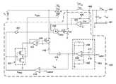
- FIG. 1illustrates a diagram of an embodiment of a power converter constructed according to the principles of the present invention
- FIG. 2illustrates a diagram of portions of the power converter illustrated in FIG. 1 constructed according to the principles of the present invention
- FIG. 3illustrates a waveform diagram of an exemplary operation associated with a power switch of a power converter in accordance with the principles of the present invention
- FIG. 4illustrates a diagram of an embodiment of portions of a power converter constructed according to the principles of the present invention
- FIGS. 5A to 5Dillustrate waveform diagrams of exemplary operations of a power converter in accordance with the principles of the present invention
- FIGS. 6A and 6Billustrate waveform diagrams of exemplary operations associated with a power switch of a power converter in accordance with the principles of the present invention
- FIGS. 7 and 8illustrate flow diagrams of embodiments of methods of operating a controller in accordance with the principles of the present invention
- FIGS. 9A and 9Billustrate waveform diagrams of exemplary operations associated with power switches of a power converter in accordance with the principles of the present invention
- FIGS. 10 and 11illustrate flow diagrams of embodiments of methods of operating a controller in accordance with the principles of the present invention
- FIGS. 12 to 14illustrate schematic drawings of embodiments of portions of power converters constructed according to the principles of the present invention.
- FIGS. 15 and 16illustrate schematic drawings of embodiments of portions of controllers constructed according to the principles of the present invention.
- the present inventionwill be described with respect to exemplary embodiments in a specific context, namely, a power converter including a controller responsive to a level of output current or other parameters to regulate an output characteristic and methods of operating the same. While the principles of the present invention will be described in the environment of a power converter, any application that may benefit from a power converter, such as a power amplifier, including a controller responsive to a level of current to regulate an output characteristic is well within the broad scope of the present invention.
- the power converterincludes a power train 110 , a controller 120 , and a driver (e.g., a gate driver) 130 , and provides power to a system/load such as a microprocessor (not shown) coupled to output terminals 140 , 141 .
- the controller 120is responsive to a level of output current I out to regulate an output characteristic of the power converter. While in the illustrated embodiment the power train 110 employs a buck converter topology, those skilled in the art should understand that other converter topologies such as a forward converter topology are well within the broad scope of the present invention.
- the power train 110 of the power converterreceives an input voltage V in from a source of electrical power (represented by battery 150 ) at an input thereof and provides a regulated output voltage V out at the output terminals 140 , 141 , or other output characteristic such as an output current I out .
- the output voltage V outis generally less than the input voltage V in such that a switching operation of the power converter can regulate the output voltage V out .
- a main power switch Q mne.g., a p-channel metal oxide semiconductor field effect transistor (“MOSFET”) embodied in a p-type laterally diffused metal oxide semiconductor (“P-LDMOS”) device
- MOSFETmetal oxide semiconductor field effect transistor
- P-LDMOSlaterally diffused metal oxide semiconductor
- an inductor current I Lout flowing through the output inductor L outincreases as current flows from the input to the output of the power train 110 .
- An ac component of the inductor current I Loutis filtered by an output capacitor C out to provide the output current I out at an output of the power converter.
- the power convertergenerally operates in the PWM mode of operation, for example and without limitation, when the output current I out is of sufficient magnitude that the inductor current I Lout in the output inductor L out or in a power switch does not reverse direction.
- the main power switch Q mnis transitioned to a non-conducting state and an auxiliary power switch Q aux [e.g., an n-channel MOSFET embodied in an n-type laterally diffused metal oxide semiconductor (“N-LDMOS”) device], coupled to the output inductor L out , is enabled to conduct in response to a gate drive signal S DRV2 .
- the auxiliary power switch Q auxprovides a path to maintain a continuity of the inductor current I Lout flowing through the output inductor L out .
- the inductor current I Lout flowing through the output inductor L outdecreases.
- the duty cycle of the main and auxiliary power switches Q mn , Q auxmay be adjusted to maintain a regulation of the output voltage V out of the power converter.
- the conduction periods for the main and auxiliary power switches Q mn , Q auxmay be separated by a small time interval to avoid cross conduction therebetween and beneficially to reduce the switching losses associated with the power converter.
- the controller 120 of the power converterreceives an output characteristic (e.g., the output current I out and/or the output voltage V out ) of the power converter, and a desired output characteristic such as a desired system voltage V system from an internal source or from an external source that may be associated with the load.
- the controller 120may be coupled to a current sensor, such as current sensor 160 to sense a power converter current such as an inductor current I Lout or the output current I out .
- the controller 120may be coupled to a current sensor to sense a current in a power switch.
- a current sensormay be employed by controller 120 to select the PWM mode of operation of the power converter by comparing a sensed current with a fixed or adjustable current threshold level.
- the controller 120may also be coupled to an input characteristic (e.g., the input voltage V in ) of the power converter and to a return lead of the source of electrical power (again, represented by battery 150 ) as illustrated in FIG. 1 to provide a ground connection therefor. While only a single ground connection is illustrated in the present embodiment, those skilled in the art should understand that multiple ground connections may be employed for use within the controller 120 .
- a decoupling capacitor C decmay be coupled as illustrated in the FIGURE to the path from the input voltage V in to the controller 120 .
- the decoupling capacitor C decis generally configured to absorb high frequency noise signals associated with the source of electrical power to protect the controller 120 .
- the controller 120provides a signal (e.g., a pulse-width modulated signal S PWM ) to control the duty cycle and a frequency of the main and auxiliary power switches Q mn , Q aux of the power train 110 to regulate the output voltage V out or other output characteristic thereof.
- the controller 120in some applications may also provide a complement of the pulse-width modulated signal S PWM during the PWM mode of operation (e.g., a complementary pulse-width modulated signal S 1-PWM ) in accordance with the aforementioned characteristics.
- Any controller adapted to control at least one power switch of the power converteris well within the broad scope of the present invention.
- a controller employing digital circuitryis disclosed in U.S. Pat. No. 7,038,438, entitled “Controller for a Power Converter and a Method of Controlling a Switch Thereof,” issued May 2, 2006, to Dwarakanath, et al., and U.S. Pat. No. 7,019,505, entitled “Digital Controller for a Power Converter Employing Selectable Phases of a Clock Signal,” issued Mar. 28, 2006, to Dwarakanath, et al., which are incorporated herein by reference.
- the power converteralso includes a driver (e.g., a gate driver) 130 to provide gate drive signals S DRV1 , S DRV2 to control conductivity of the main and auxiliary power switches Q mn , Q aux , respectively, responsive to the pulse-width modulated signal S PWM (and, if necessary, the control the complementary pulse-width modulated signal S 1-PWM ) provided by the controller 120 .
- a driver 130e.g., a gate driver 130 to provide gate drive signals S DRV1 , S DRV2 to control conductivity of the main and auxiliary power switches Q mn , Q aux , respectively, responsive to the pulse-width modulated signal S PWM (and, if necessary, the control the complementary pulse-width modulated signal S 1-PWM ) provided by the controller 120 .
- a driver 130e.g., a gate driver 130 to provide gate drive signals S DRV1 , S DRV2 to control conductivity of the main and auxiliary power switches Q
- the driver 130typically includes switching circuitry incorporating a plurality of driver switches that cooperate to provide the gate drive signals S DRV1 , S DRV2 to the main and auxiliary power switches Q mn , Q aux .
- any driver 130 capable of providing the gate drive signals S DRV1 , S DRV2 to control a power switchis well within the broad scope of the present invention.
- a driveris disclosed in U.S. Pat. No. 7,330,017, entitled “Driver for a Power Converter and a Method of Driving a Switch Thereof,” issued Feb. 12, 2008, to Dwarakanath, et al., and a power switch is disclosed in U.S. Pat. No.
- the main and auxiliary power switches Q mn , Q auxare typically power switches that can be incorporated into a semiconductor device in an integrated circuit proximate control or signal processing devices that perform many of the control functions of the controller 120 of the power converter.
- the control and signal processing devicesare typically complementary metal-oxide semiconductor (“CMOS”) devices such as p-type metal oxide semiconductor (“PMOS”) devices and n-type metal oxide semiconductor (“NMOS”) devices.
- CMOScomplementary metal-oxide semiconductor
- PMOSp-type metal oxide semiconductor
- NMOSn-type metal oxide semiconductor
- the PMOS and NMOS devicesmay also be referred to as p-channel and n-channel MOSFETs, respectively.
- the duty cycle of a power switchdetermines the steady-state ratio of a power converter output voltage V out to its input voltage V in .
- a controllertypically regulates an output characteristic of a power converter by controlling a duty cycle of a power switch. Duty cycle is generally controlled by comparing a sawtooth voltage waveform with a controlled threshold voltage produced by an error amplifier configured to sense an output voltage or other output characteristic.
- a load coupled to a power convertermay sometimes operate for a period of time in an idle mode wherein the load draws a relatively small but non-zero current from the power converter, for example, less than one percent of its normal load current. Under such operating conditions, wherein power conversion efficiency of the power converter is typically very low, it is preferable to provide high power conversion efficiency, particularly when the power converter is powered from a portable energy source such as a battery.
- a switch-current control subsystem 200 of the power converteris configured to control a current flowing through a main power switch Q mn during the complementary duty cycle 1-D of a switching cycle.
- the switch-current control subsystem 200includes a gate driver 201 for the main power switch Q mn .
- the gate driver 201includes driver switches such as a p-channel field-effect transistor (“FET”) 224 and an n-channel FET 222 , with their gates coupled together and driven by a pulse-width modulated signal S PWM .
- the pulse-width modulated signal S PWMmay be created by a controller such as the controller 120 illustrated and described with respect to FIG. 1 .
- the source, gate, and drain of the respective driver switchesare labeled with “s,” “g,” and “d,” respectively.
- Producing a current flowing through the main power switch Q mn during the complementary duty cycle 1-D of a switching cycle when a power converter is lightly loaded, such as producing less than five percent of its rated output power,can provide substantial efficiency improvement over a switching mode wherein both the main and auxiliary power switches Q mn , Q aux are continuously enabled to conduct in complementary intervals of time.
- a switching mode wherein the main and auxiliary power switches Q mn , Q aux are enabled to conduct in complementary intervals of timecan produce substantial bidirectional current through reactive circuit elements, such as an output inductor L out , contributing thereby substantial power losses.
- producing a light current flowing through the main power switch Q mn during the complementary duty cycle 1-D of a switching cycle when a power converter is lightly loadedcan be a more economical alternative than providing a large output capacitance to maintain an output voltage V out of a power converter during a mode of operation wherein all switching is temporarily disabled.
- the switch-current control subsystem 200 illustrated in FIG. 2is configured to control a gate voltage for the main power switch Q mn when it would ordinarily be disabled to conduct (i.e., during the complementary duty cycle 1-D of a switching cycle).
- the gate voltage of the main power switch Q mnis controlled during the complementary duty cycle 1-D of a switching cycle so that the main power switch Q mn can conduct a controlled, light current to the load (i.e., an output current I out of the power converter).
- the gate driver 201couples the gate of the main power switch Q mn to ground, turning it on.
- the gate driver 201couples the gate of the main power switch Q mn to the output of an operational amplifier 214 .
- the output of the operational amplifier 214is controlled to enable the main power switch Q mn to conduct a controlled, light current (e.g., a controlled current level such as a remnant current level) when the pulse-width modulated signal S PWM is low.
- a p-channel FET 212 with its gate coupled to its drainoperates as a diode in forward conduction.
- the drain current of the p-channel FET 212is controlled by a resistor 216 , which is coupled substantially across the input voltage V in (less the diode drop of the p-channel FET 212 ).
- the gate of the p-channel FET 212is set to the voltage with respect to its source that is necessary to conduct the current flowing through the resistor 216 .
- This gate voltageis sensed with the operational amplifier 214 and coupled to the gate of the main power switch Q mn during the complementary duty cycle 1-D of a switching cycle.
- the p-channel FET 212 and the main power switch Q mnoperate as a current mirror during the complementary duty cycle 1-D of a switching cycle, wherein a current controlled by the resistor 216 and scaled by a die geometric ratio of the main power switch Q mn to the p-channel FET 212 flows through the main power switch Q mn .
- the p-channel FET 212 and the main power switch Q mnare produced in a common manufacturing process and are configured to operate at substantially the same die temperature.
- the p-channel FET 212is a downscaled replica of the main power switch Q mn .
- the operation of current mirrorsis well known in the art, and will not be described further in the interest of brevity.
- FIG. 3illustrated is a waveform diagram of an exemplary operation associated with a power switch of a power converter in accordance with the principles of the present invention.
- the waveformrepresents a source-to-drain current I Qmnsd flowing through a power switch (e.g., the main power switch Q mn of FIG. 2 ) wherein the output current is of sufficient magnitude that current in an output inductor or in a semiconductor power switch does not reverse direction.
- the source-to-drain current I Qmnsd flowing through the main power switch Q mnincreases substantially linearly due to the voltage applied across an output inductor (e.g., the output inductor L out of FIG. 2 ).
- the source-to-drain current I Qmnsdmaintains a controlled, substantially constant current level (e.g., a remnant current level) I CC flowing through the main power switch Q mn that is controlled by a controller such as the switch-current control subsystem 200 of FIG. 2 .
- a controllersuch as the switch-current control subsystem 200 of FIG. 2 .
- FIG. 4illustrated is a diagram of an embodiment of portions of a power converter constructed according to the principles of the present invention.
- a controller 400 of the power converteris operable in different modes of operation.
- the controller 400regulates an output characteristic of the power converter, and is configured to control current (e.g., a controlled or remnant current level I CC ) through a main power switch Q mn in response to a sensed or estimated power converter current.
- the controller 400is advantageously operable to provide a mode of operation wherein improved power conversion efficiency is achieved at light load.
- the power convertermay experience an improvement in dynamic response because of an additional bias available to feed an output thereof that in turn produces a smaller decay of an output characteristic (e.g., an output voltage V out ) since the output voltage V out is not supplied only by an output capacitor C out .
- the power converterincludes an error amplifier 402 that senses the output voltage V out as an output characteristic to provide a feedback signal.
- the primary and complementary duty cycles D, 1-D of a switching cycleare established by a comparator 414 that produces a pulse-width modulated signal S PWM .
- the noninverting input of the comparator 414is coupled to an error amplifier signal V EA of the error amplifier 402 .
- the inverting input of the comparator 414is coupled to a sawtooth waveform signal V sawtooth that has a substantial positive voltage offset for the waveform valleys.
- a substantial current(an output current I out ) is delivered to a load (not shown) coupled to output terminals 440 , 441
- the main and auxiliary power switches Q mn , Q auxare alternately enabled to conduct, respectively, during a primary duty cycle D and a complimentary duty cycle 1-D.
- the primary duty cycle D and the complementary duty cycle 1-Dare controlled to regulate an output characteristic of the power converter.
- the load currenti.e., an output current I out of the power converter
- the load currentis of sufficient magnitude so that an inductor current I Lout flowing through output inductor L out does not reverse direction.
- the main power switch Q mnconducts a current controlled (e.g., a controlled current level I CC ) by a current mirror including a gate driver 401 , an operational amplifier 404 , a p-channel FET 408 and a resistor 416 .
- the current mirroris operable in a manner similar to that described with reference to FIG. 2 .
- the current through the main power switch Q mnis controlled by current flowing through the resistor 416 .
- the resistor 416is coupled to the error amplifier signal V EA via an inverter 418 .
- the inverter 418amplifies the output of the error amplifier 402 with gain ⁇ k.
- the current flowing through the resistor 416is also reduced.
- the current flowing through the main power switch Q mn during the complementary duty cycle 1-D of the switching cycleis also reduced.
- the error amplifier 402senses the output voltage V out .
- the error amplifier 402includes an operational amplifier 409 that includes feedback networks 405 , 406 .
- the feedback networks 405 , 406include a parallel arrangement of a capacitor and a resistor.
- the error amplifier 402further includes input networks including resistors 410 , 412 .
- the values of components in feedback networks 405 , 406are equal, and the values of the resistors 410 , 412 in the input networks are equal.
- the error amplifier 402generates the error amplifier signal V EA in response to the sensed output voltage V out of the power converter and a desired system voltage V system .
- the controller 400enables alternating conduction of the main and auxiliary power switches Q mn , Q aux while enabling a controlled current (e.g., a controlled current level I CC ) flowing through the main power switch Q mn during the complementary duty cycle 1-D.
- the controlled current flowing through the main power switch Q mnis responsive to the error amplifier signal V EA produced by the error amplifier 402 .
- a second mode operation(also referred to as a hybrid mode of operation) the power converter output current I out is insufficient to sustain unidirectional current flow in the output inductor L out as described with respect to the PWM mode of operation.
- Bidirectional current flow through output inductor L outis prevented in the power converter illustrated in FIG. 4 by sensing the inductor current I Lout with a current sensor 460 .
- the sensed inductor current I Loutis amplified with a transresistance amplifier that includes operational amplifier 426 coupled to feedback resistor 428 .
- the gain of the transresistance amplifieris substantially the resistance of the resistor 428 .
- the output of the transresistance amplifieris coupled to an input of an AND gate 420 .
- the output of the comparator 414is coupled to a signal inverter 422 .
- the signal inverter 422produces a high output signal during the complementary duty cycle 1-D of the switching cycle.
- the output of the signal inverter 422is coupled to the other input of the AND gate 420 .
- the AND gate 420produces a high gate drive signal S DRV2 for the auxiliary power switch Q aux to enable conduction therein during the complementary duty cycle 1-D of the switching cycle, when positive inductor current I Lout flows through the output inductor L out .
- the polarity of the current sensor 460is selected, as would be known by one with ordinary skill in the art, to produce a sense of the signal at the output of operational amplifier 426 to enable conduction in the auxiliary power switch Q aux during the complementary duty cycle 1-D of the switching cycle, when positive current flows through the output inductor L out .
- the current mirrorpreviously described continues to provide a gate drive signal S DRV1 for the main power switch Q mn to enable a current controlled by the error amplifier 402 to flow therethrough during the complementary duty cycle 1-D of the switching cycle.
- a controlled currente.g., a controlled current level I CC
- the controlleris configured to control a level of current (again, e.g., a controlled current level I CC ) in the main power switch Q mn when the auxiliary power switch Q aux is substantially disabled to conduct (e.g., during the complementary duty cycle 1-D of the switching cycle).
- a third mode operation(also referred to as a light current mode of operation)
- the output current I outis further reduced so that a source-to-drain current that flows through the main power switch Q mn is controlled to the controlled current level I CC to maintain sufficient current to power the load.
- the error amplifier 402can be used to control current flowing to the output terminal 440 , thereby regulating an output characteristic of the power converter.
- the alternately enabled conduction of the main and auxiliary power switches Q mn , Q auxis disabled, since the source-to-drain current that flows through the main power switch Q mn is sufficient to power the load.
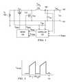
- FIGS. 5A to 5Dillustrated are waveform diagrams of exemplary operations of a power converter in accordance with the principles of the present invention.
- the waveform diagramswill be described in part with reference to signals and components illustrated and described with respect to FIG. 4 .
- a left portion of FIG. 5Aillustrates an error amplifier signal V EA produced by the error amplifier 402 and a voltage sawtooth signal V sawtooth produced by a sawtooth voltage generator (not shown) in the PWM mode of operation.
- the comparator 414 illustrated in FIG. 4sets the primary duty cycle D of the switching cycle.
- FIG. 5AIn the right portion of FIG. 5A is a graphical representation of the resulting inductor current I Lout that flows through the output inductor L out .
- the load currente.g., an output current I out of the power converter
- the load currentis sufficiently high so that inductor current I Lout in the output inductor L out does not reverse.
- FIG. 5Billustrated in the left portion of the FIGURE again is a graphical representation of the error amplifier signal V EA produced by the error amplifier 402 and the voltage sawtooth signal V sawtooth produced by a sawtooth voltage generator, again in the PWM mode of power converter operation.
- the inductor current I Lout flowing through the output inductor L outis again illustrated.
- the inductor current I Lout flowing through output inductor L outreaches zero at the end of the switching cycle, but does not reverse direction, and thus preserving operation in the PWM mode of operation.
- FIG. 5Cillustrated in the left portion of the FIGURE is a graphical representation of the error amplifier signal V EA produced by the error amplifier 402 and the voltage sawtooth signal V sawtooth produced by a sawtooth voltage generator in a hybrid mode of operation.
- the inductor current I Lout flowing through the output inductor L outis again illustrated.
- the inductor current I Lout flowing through the output inductor L outwould reach zero and reverse direction during the complementary duty cycle 1-D.
- the output current I outis insufficient to prevent current reversal in output inductor L out unless accommodation is provided in the power converter. Accommodation is provided by the AND gate 420 illustrated in FIG.
- FIG. 5Dillustrated in the left portion of the FIGURE is a graphical representation of the error amplifier signal V EA produced by the error amplifier 402 and the voltage sawtooth signal V sawtooth produced by a sawtooth voltage generator in a light current mode of operation.
- the output current I outhas been reduced even further so that output current I out can be sustained by the controlled current level I CC flowing through the main power switch Q mn without alternately enabling conduction through the main and auxiliary power switches Q mn , Q aux .
- a reduced voltage level for the error amplifier signal V EA produced by the error amplifier 402causes the error amplifier signal V EA to lie below even the valleys of the sawtooth waveform signal V sawtooth .
- the comparator 414produces no duty cycle (e.g., disabling the duty cycle).
- the inductor current I Loutthat flows through the output inductor L out is maintained at the controlled current level I CC flowing through the main power switch Q mn , controlled by the error amplifier 402 by means of the current mirror as described previously.
- the resultis an output current I out controlled by the error amplifier 402 that flows to the load without active switching of either the main power switch Q mn or the auxiliary power switch Q aux . Little to no ripple current is produced, and switching losses are substantially eliminated. Power conversion efficiency in this mode of operation is substantially improved and is determined by the ratio of output voltage V out to input voltage V in and remaining losses in the power converter elements. In this mode of operation, some controller elements can be selectively disabled to further reduce power losses.
- the level of controlled current level I CC for the main power switch Q mnis not controlled by the error amplifier 402 in response to actual load current at light levels of load current (i.e., a preselected level of controlled current level I CC is chosen), it is important that the preselected level of controlled current level I CC for the main power switch Q mn be less than the expected level of load current (again, the output current I out of the power converter) when the load is in a low-current state. Otherwise, the output voltage V out of the power converter can increase beyond a desired voltage level.
- FIGS. 6A and 6Billustrated are waveform diagrams of exemplary operations associated with a power switch of a power converter in accordance with the principles of the present invention.
- the waveform diagramswill be described in part with reference to signals and components illustrated and described with respect to FIG. 4 .
- FIG. 6Aillustrates a graphical representation of a primary duty cycle D resulting from the error amplifier signal V EA produced by the error amplifier 402 .
- the error amplifier signal V EAis less than a threshold level 605 , no duty cycle is produced (e.g., disabling the duty cycle).
- the primary duty cycle Dincreases linearly with the error amplifier signal V EA until it reaches 100%.
- the error amplifier 402is constructed to produce an error amplifier signal V EA that can fall below the minimum voltage of the sawtooth waveform signal V sawtooth to provide a mode of operation wherein no duty cycle is produced (e.g., disabling the duty cycle).
- FIG. 6Billustrated is a graphical representation of a controlled or remnant current level I CC that flows through the main power switch Q mn during, for instance, the complementary duty cycle 1-D of the switching cycle as a function of the error amplifier signal V EA produced by the error amplifier 402 .
- the controlled current level I CCattains a saturation level 615 .
- the controlled current level I CCis reduced as the error amplifier signal V EA increases beyond the error amplifier voltage level 610 produced by the error amplifier 402 as represented by dashed line 620 . While the controlled current level I CC illustrated in FIG. 6B are represented by straight lines, it is contemplated that these lines may be implemented as nonlinear functions of the error amplifier signal V EA to produce further efficiency enhancements associated with a particular application.
- the power converterincludes a controller configured to provide a plurality of modes of operation.
- a PWM mode of operationthe main and auxiliary power switches are alternately enabled to conduct in substantially complementary portions of a switching cycle in response to an output characteristic, such as an output voltage of the power converter.
- a beginning time of a switching cycleis ordinarily controlled by a switching cycle (e.g., frequency) clock.
- the controllercontrols the level of current in the main power switch with an error amplifier with an input coupled to an output characteristic of the power converter such an output voltage.
- the controllercontrols the level of current (e.g., a controlled current level such as a remnant current level) in the main power switch during the complementary duty cycle 1-D of the switching cycle when the auxiliary power switch is enabled to conduct (i.e., during an interval of time that begins substantially after the auxiliary power switch is enabled to conduct and ends substantially when the main power switch enabled to conduct).
- the controllermay employ a current mirror to control the remnant current level in the main power switch.
- the controllerpreferably reduces the remnant current level in the main power switch during the complementary duty cycle 1-D in response to an increase of a sensed current of the power converter, such as an output current.
- the controllerIn a light current mode of operation (which may occur after the PWM mode of operation), when a current detected in the auxiliary power switch is less than a current threshold level, the controller disables the alternately enabled conduction of the main and auxiliary power switches and controls a remnant current level in the main power switch to regulate the output characteristic.
- the controllerincludes an error amplifier coupled to an output characteristic of the power converter such as the output voltage of the power converter to control the remnant current level in the main power switch.
- the controllerselectively disables controller elements such as the operational amplifier 409 of the error amplifier 402 and the comparator 414 illustrated in FIG. 4 and the bias sources thereto.
- the main and auxiliary power switchesare alternately enabled to conduct in substantially complementary portions of a switching cycle in response to an output characteristic, such as an output voltage of the power converter.
- the controllercontrols a conduction of the main power switch to provide a level of current (e.g., a controlled current level such as a remnant current level) in the main power switch when a level of current in the main power switch crosses an upper current threshold level, which may be a fixed upper current threshold level.
- the controlleralso enables conduction in the auxiliary power switch when the level of current in the main power switch crosses the upper current threshold level.
- the controllermay also perform the aforementioned operations in accordance with monitoring an inductor current (as opposed or in addition to the current in the main power switch) of an output inductor of a power converter employing the main and auxiliary power switches. Thereafter, the controller disables conduction in the auxiliary power switch when a level of current in the auxiliary power switch crosses a lower current threshold level (e.g., approximately zero current) to prevent reverse current flow in an output inductor or the auxiliary power switch.
- a lower current threshold levele.g., approximately zero current
- the controllertransitions between modes of operation by testing operational parameters in the power converter.
- the controllertransitions to the light current mode of operation when a level of current in the auxiliary power switch or in the output inductor is reduced to a current threshold level such as zero current when a discontinuous current mode (“DCM”) is reached.
- DCMdiscontinuous current mode
- the controllertransitions from the light current mode of operation to the recharge mode of operation and resets a switching cycle counter when an output characteristic falls below a lower output characteristic threshold level such as a lower output voltage threshold level.
- the controllertransitions back to the PWM mode of operation when a switching cycle counter exceeds a predetermined count.
- the controllertransitions to the light current mode of operation when the output characteristic such as the output voltage exceeds an upper output characteristic threshold level, such as an upper output voltage threshold level.
- the controllerenables conduction in the main power switch with a switching cycle clock (e.g., a switching cycle clock employed to initiate a switching cycle).
- a switching cycle clocke.g., a switching cycle clock employed to initiate a switching cycle.
- FIG. 7illustrated is a flow diagram of an embodiment of a method of operating a controller in accordance with the principles of the present invention.
- the methodmay begin at one of the described modes of operation.
- the controllermay begin in a recharge mode of operation and follow the method of operation therefrom as provided below.
- the controllersamples a current, such as an auxiliary power switch current I auxsw (or an inductor current in an output inductor of a power converter), and compares the auxiliary power switch current I auxsw to a current threshold level I thresh , in a step or module 705 . If the auxiliary power switch current I auxsw is less than the current threshold level I thresh the controller sets a flag F PWM to zero in a step or module 710 to disable the PWM mode of operation and transitions to a light current mode of operation. Otherwise, the controller continues in the PWM mode of operation and iteratively performs step 705 until the auxiliary power switch current I auxsw exceeds the current threshold level I thresh or the controller changes the mode of operation based on another process therein.
- a currentsuch as an auxiliary power switch current I auxsw (or an inductor current in an output inductor of a power converter)
- the controllercompares an output characteristic (e.g., an output voltage V out ) of the power converter to a lower output characteristic threshold level (e.g., a lower output voltage threshold level V lower ) in a step or module 715 . If the output voltage V out is less than the lower output voltage threshold level V lower , the controller resets a switching cycle counter, for example, to zero in a step or module 720 , and transitions to a recharge mode of operation. Otherwise, the controller continues in the light current mode of operation and iteratively performs step 715 until the output voltage V out exceeds the lower output voltage threshold level V lower or the controller changes the mode of operation based on another process therein
- the controllerincrements the switching cycle counter in a step or module 725 and executes a switch logic in a step or module 730 as described below with respect to FIG. 8 .
- the controllercompares the count of the switching cycle counter to a predetermined count such as a maximum count (designated “count_max”) in a step or module 735 . If the count exceeds the maximum count, the controller sets a flag F PWM equal to one to enable the PWM mode of operation in the following switching cycle in a step or module 740 and then exits to the PWM mode of operation.
- the controllercompares an output characteristic (e.g., an output voltage V out ) of the power converter to an upper output characteristic threshold level (e.g., an upper output voltage threshold level V upper ) in a step or module 745 . If the output voltage V out is greater than the upper output voltage threshold level V upper , the controller transitions to the light current mode of operation. Otherwise, the controller continues in the recharge mode of operation and iteratively performs steps 725 , et seq., until the controller changes the mode of operation based thereon or another process therein.
- an output characteristice.g., an output voltage V out
- V upper output characteristic threshold levele.g., an upper output voltage threshold level V upper
- FIG. 8illustrated is a flow diagram of an embodiment of a method of operating a controller in accordance with the principles of the present invention.
- the exemplary method of FIG. 8demonstrates an operation of the switch logic introduced above with respect to FIG. 7 .
- the controllerdetermines if a new switching cycle is beginning (e.g., as indicated by a time 910 illustrated in FIGS. 9A and 9B below). If a new switching cycle is beginning, the controller sets a flag F D to one to enable conduction of a main power switch in a step or module 810 . If it is not the beginning of a new switching cycle, the controller determines if the flag F D is equal to one in a step or module 815 .
- the controllerdetermines if a main power switch current I auxsw or an inductor current I Lout in an output inductor exceeds an upper current threshold level I upper in a step or module 820 . If the main power switch current I mnsw or an inductor current I Lout exceeds the upper current threshold level I upper , the flag F D is reset to zero and a conductivity of the main power switch is reduced to provide a controlled current level (e.g., a remnant current level) in a step or module 825 . Additionally, a flag F 1-D is set to one to enable conduction of an auxiliary power switch in the step or module 825 . If the main power switch current I mnsw or an inductor current I Lout does not exceed the upper current threshold level I upper , the controller continues the conduction of the main power switch and iteratively performs step 815 , et seq.
- a main power switch current I auxsw or an inductor current I Lout in an output inductorexceeds an
- the controllerdetermines if a flag F 1-D is equal to one in a step or module 830 . If the value of the flag F 1-D is not equal to one, the controller returns to step 805 or performs other processes therein. If the value of the flag F 1-D is equal to one (see also step or module 825 introduced above), the controller determines if an auxiliary power switch current I auxsw is less than a lower current threshold level I lower in a step or module 835 . If the auxiliary power switch current I auxsw is less than the lower current threshold level I lower , the flag F 1-D is reset to zero and a conductivity of the auxiliary power switch is disabled in a step or module 840 .
- the controllermay return to step 805 or perform other processes therein. If the auxiliary power switch current I auxsw is not less than the lower current threshold level I lower , the controller continues the conduction of the auxiliary power switch and iteratively performs step 830 , et seq.
- FIGS. 9A and 9Billustrated are waveform diagrams of exemplary operations associated with power switches of a power converter in accordance with the principles of the present invention.
- the waveformsillustrate currents flowing through main and auxiliary power switches in a recharge mode of operation.
- the waveform 905represents current flowing through the main power switch during a switching cycle of period ⁇ T s that begins at time 910 and ends at time 915 .
- the current in the main power switchis enabled to conduct at the time 910 by a switching cycle clock.
- the current in the main power switchincreases until it reaches an upper current threshold level (“I upper ”) at time 920 , at which time conductivity of the main power switch is reduced to provide a controlled current level (e.g., a remnant current level L cc ) by the controller.
- I upperan upper current threshold level
- L cca remnant current level
- conductivity of the auxiliary power switchis enabled to conduct as represented by the waveform 925 .
- the current in the auxiliary power switchdecreases until it crosses a lower current threshold level (“I lower ”) at time 930 , and remains substantially zero until the end of the switching cycle at time 915 .
- FIG. 10illustrated is a flow diagram of an embodiment of a method of operating a controller in accordance with the principles of the present invention.
- the methodmay begin at one of the described modes of operation.
- the controllermay begin in a recharge mode of operation and follow the method of operation therefrom as provided below.
- the controllersamples a current, such as an auxiliary power switch current I auxsw (or an inductor current in an output inductor of a power converter), and compares the auxiliary power switch current I auxsw to a current threshold level I thresh , in a step or module 1005 . If the auxiliary power switch current I auxsw is less than the current threshold level I thresh , the controller sets a flag F PWM to zero in a step or module 1010 to disable the PWM mode of operation and transitions to a light current mode of operation. Otherwise, the controller continues in the PWM mode of operation and iteratively performs step 1005 until the auxiliary power switch current I auxsw exceeds the current threshold level I thresh or the controller changes the mode of operation based on another process therein.
- a currentsuch as an auxiliary power switch current I auxsw (or an inductor current in an output inductor of a power converter)
- the controllercan advantageously transition to the light current mode of operation when DCM is reached.
- a controlled current levele.g., a remnant current level
- the controllercontrols the remnant current level employing a current mirror in response to an output characteristic of the power converter.
- the controllermay reduce the remnant current level in response to an increase of a sensed current of the power converter, such as a sensed output current.
- the controllercompares an output characteristic (e.g., an output voltage V out ) of the power converter to a lower output characteristic threshold level (e.g., a lower output voltage threshold level V lower ) in a step or module 1015 . If the output voltage V out is less than the lower output voltage threshold level V lower , the controller resets a switching cycle counter, for example, to zero in a step or module 1020 , and transitions to a recharge mode of operation. Otherwise, the controller continues in the light current mode of operation and iteratively performs step 1015 until the output voltage V out exceeds the lower output voltage threshold level V lower or the controller changes the mode of operation based on another process therein.
- an output characteristice.g., an output voltage V out
- V lower output characteristic threshold levele.g., a lower output voltage threshold level V lower
- the main and auxiliary power switchesare alternately enabled to conduct, and conduction in the main power switch is reduced to a remnant current level when a level of current in the main power switch (or an output inductor) increases to an upper current threshold level, which may be a fixed or adjustable upper current threshold level.
- Conduction in the auxiliary power switchis terminated when a level of current in the auxiliary power switch is reduced to a lower current threshold level, which may be a fixed or adjustable lower current threshold level of substantially zero current.
- the remnant current levelis controlled by the controller responsive to the output characteristic of the power converter.
- the controllerinitiates conduction by the main power switch with the switching cycle clock.
- the controllercompares the count of a switching cycle counter to a predetermined count such as a maximum count (designated “count_max”) in a step or module 1025 . If the count exceeds the maximum count, the controller transitions to a hybrid mode of operation. Otherwise, the controller executes a switch logic in a step or module 1030 as described above with respect to FIG. 8 . The controller then compares an output characteristic (e.g., an output voltage V out ) of the power converter to an upper output characteristic threshold level (e.g., an upper output voltage threshold level V upper ) in a step or module 1035 . If the output voltage V out is greater than the upper output voltage threshold level V upper , the controller transitions to the light current mode of operation.
- a predetermined countsuch as a maximum count (designated “count_max”) in a step or module 1025 . If the count exceeds the maximum count, the controller transitions to a hybrid mode of operation. Otherwise, the controller executes a switch logic in a step or module 1030 as described above
- the controllerincrements the switching cycle counter in a step or module 1040 , continues in the recharge mode of operation and iteratively performs steps 1025 , et seq., until the controller changes the mode of operation based thereon or another process therein.
- the main and auxiliary power switchesare alternately enabled to conduct in the substantially complementary portions of the switching cycle.
- the alternately enabled conductionis ordinarily controlled by an error amplifier coupled to the output characteristic of the power converter.
- conduction in the auxiliary power switchis terminated when a level of current in the auxiliary power switch is reduced to a lower current threshold level.
- Conduction in the auxiliary power switchis terminated to prevent a reverse current flowing through the output inductor of the power converter. A small reverse current flowing through the output inductor may be allowed to enable soft switching of the main power switch.
- a remnant current level in the main power switchis controlled in an interval of time that begins substantially when the auxiliary power switch is enabled to conduct and ends substantially when the main power switch is enabled to conduct (i.e., during a complementary duty cycle 1-D).
- the controlleremploys an error amplifier coupled to the output terminal of the power converter to control the remnant current level.
- the switching cycleis terminated prior to the start time of the next switching cycle that is ordinarily controlled by the switching cycle clock.
- conduction in the main power switchcan also be reduced to the remnant current level prior to a main power switch conduction termination time controlled by the error amplifier (i.e., during the primary duty cycle D).
- the controllercompares an output characteristic (e.g., an output voltage V out ) of the power converter to an upper output characteristic threshold level (e.g., an upper output voltage threshold level V upper ) in a step or module 1045 . If the output voltage V out is greater than the upper output voltage threshold level V upper , the flag F D is reset to zero and a conductivity of the main power switch is reduced to provide a controlled current level (e.g., a remnant current level) in a step or module 1050 . Additionally, a flag F 1-D is set to one to enable conduction of an auxiliary power switch in the step or module 1050 .
- an output characteristice.g., an output voltage V out
- an upper output characteristic threshold levele.g., an upper output voltage threshold level V upper
- the flag F Dis reset to zero and a conductivity of the main power switch is reduced to provide a controlled current level (e.g., a remnant current level) in a step or module 1050 .
- a flag F 1-Dis
- the controllercompares an output characteristic (e.g., the output voltage V out ) of the power converter to a lower output characteristic threshold level (e.g., a lower output voltage threshold level V lower ) in a step or module 1055 . If the output voltage V out is less than the lower output voltage threshold level V lower , the controller terminates the switching cycle prior to the start time of the next switching cycle in a step or module 1060 .
- an output characteristice.g., the output voltage V out
- a lower output characteristic threshold levele.g., a lower output voltage threshold level V lower
- the controllercompares a time (e.g., a duration of time operating in the hybrid mode of operation) to a predetermined or a maximum time (designated “timeout_max”) in a step or module 1065 .
- the maximum timemay be computed by adding a time increment, such as 600 microseconds, to the time when the controller enters the hybrid mode of operation. If the time is greater than the maximum time, the controller sets a flag F PWM equal to one in a step or module 1070 to signal a transition to the PWM mode of operation in the next switching cycle. Otherwise, the controller continues in the hybrid mode of operation and iteratively performs step 1045 , et seq. for the time window defined by the maximum time.
- adaptation of a duty cycleis made from time to time in, for instance, a PWM mode of operation to enable detection of a reverse or low level of current flow in an auxiliary power switch or output inductor.
- a PWM mode of operationto enable detection of a reverse or low level of current flow in an auxiliary power switch or output inductor.
- the controllermay not make an accurate or reliable determination of the need to enter into the light current mode of operation.
- the controllerfrom time to time limits a duty cycle of the auxiliary power switch, preferably for one switching cycle.
- the controllermay limit a duty cycle for one switching cycle for the auxiliary power switch periodically every sixty-four switching cycles and a corresponding increase a duty cycle for the main power switch during that switching cycle to preserve a switching frequency.
- the duty cycle of the auxiliary power switchis accordingly periodically limited, preferably for one switching cycle, after a number of switching cycles. Such infrequent modification of a duty cycle, which need not be periodic, produces a small deviation in an output characteristic such as an output voltage from a desired regulated value, which is generally not detrimental to the operation of the power converter.
- FIG. 11illustrated is a flow diagram of an embodiment of a method of operating a controller in accordance with the principles of the present invention.
- the methodmay begin at one of the described modes of operation.
- the controllermay begin in a recharge mode of operation and follow the method of operation therefrom as provided below.
- the main and auxiliary power switchesare alternately enabled to conduct in substantially complementary portions of a switching cycle in response to an output characteristic such as an output voltage of the power converter.
- a duty cycleis periodically limited for one switching cycle to facilitate detection of a reverse or low level of current flow in an auxiliary power switch or in an output inductor. If a switching cycle counter is greater than a predetermined count such as a maximum count (designated “count_max”) as illustrated in a step or module 1105 , then the duty cycle of a main power switch is increased (e.g., to a maximum value) and, correspondingly, the duty cycle of the auxiliary power switch is limited (e.g., to a minimum value) in a step or module 1110 .
- the predetermined or maximum countmay correspond to 64 switching cycles.
- the controllersamples a current, such as an auxiliary power switch current I auxsw (or an inductor current in an output inductor of a power converter), and compares the auxiliary power switch current I auxsw to a current threshold level I thresh in a step or module 1115 . If the auxiliary power switch current I auxsw is less than the current threshold level I thresh , the controller sets a flag F PWM to zero in a step or module 1120 to disable the PWM mode of operation and transitions to a light current mode of operation.
- a currentsuch as an auxiliary power switch current I auxsw (or an inductor current in an output inductor of a power converter)
- the switching cycle counter(“count”) is incremented as illustrated in a step or module 1125 and the controller continues in the PWM mode of operation and iteratively performs steps 1105 , et seq. until the controller changes the mode of operation based thereon or another process therein.
- a duty cycleis periodically limited for one switching cycle.
- the duty cycle limitneed not be periodic, and the limit may be applied for more than one switching cycle to facilitate the current detection.
- the controllercompares an output characteristic (e.g., an output voltage V out ) of the power converter to a lower output characteristic threshold level (e.g., a lower output voltage threshold level V lower ) in a step or module 1130 . If the output voltage V out is less than the lower output voltage threshold level V lower , the controller resets a switching cycle counter, for example, to zero in a step or module 1140 , and transitions to a recharge mode of operation. Otherwise, the controller continues in the light current mode of operation and iteratively performs step 1130 until the output voltage V out exceeds the lower output voltage threshold level V lower or the controller changes the mode of operation based on another process therein.
- an output characteristice.g., an output voltage V out
- V lower output characteristic threshold levele.g., a lower output voltage threshold level V lower
- the controllercompares the count of a switching cycle counter to a predetermined count such as a maximum count (designated “count_max”) in a step or module 1150 . If the count exceeds the maximum count, the controller sets a flag F PWM equal to one in a step or module 1155 , resets a switching cycle counter, for example, to zero in a step or module 1160 , and transitions to the PWM mode of operation.
- count_maxa predetermined count
- the controllersets a flag F PWM equal to one in a step or module 1155 , resets a switching cycle counter, for example, to zero in a step or module 1160 , and transitions to the PWM mode of operation.
- the maximum count that enables the transition from the recharge mode of operation to the PWM mode of operationmay be different from the maximum count employed in the PWM mode of operation to limit a duty cycle of a power switch.
- the controllerexecutes a switch logic in a step or module 1165 as described above with respect to FIG. 8 .
- the controllercompares an output characteristic (e.g., an output voltage V out ) of the power converter to an upper output characteristic threshold level (e.g., an upper output voltage threshold level V upper ) in a step or module 1170 . If the output voltage V out is greater than the upper output voltage threshold level V upper , the controller transitions to the light current mode of operation. Otherwise, the controller increments the switching cycle counter in a step or module 1175 , continues in the recharge mode of operation and iteratively performs steps 1150 , et seq., until the controller changes the mode of operation based thereon or another process therein.
- an output characteristice.g., an output voltage V out
- V upper output characteristic threshold levele.g., an upper output voltage threshold level V upper
- FIG. 12illustrated is a schematic drawing of an embodiment of portions of a power converter constructed according to the principles of the present invention.
- the power converterincludes a controller having an error amplifier 1205 that compares a desired system voltage V system with an output voltage V out of the power converter.
- An error amplifier signal 1210 from the error amplifier 1205is coupled to control subsystem 1215 that includes mode transition logic.
- a first comparator 1220compares the output voltage V out of the power converter with an upper output voltage threshold level V upper to produce a first comparator signal 1225 , which is coupled to the control subsystem 1210 to enable a mode transition from a recharge mode of operation to a light current mode of operation.
- a second comparator 1230compares the output voltage V out of the power converter with a lower output voltage threshold level V lower to produce a second comparator signal 1235 , which is coupled to the controller subsystem 1215 to enable a mode transition from a light current mode of operation to a recharge mode of operation.
- a third comparator 1240compares a sensed inductor current I Lout in an output inductor L out with a current threshold level I thresh to produce a third comparator signal 1245 , which is coupled to the controller subsystem 1215 to enable a mode transition from a PWM mode of operation to a light current mode of operation.
- the third comparator 1240may compare a sensed current in a power switch with the current threshold level I thresh to produce the third comparator signal 1245 .
- the threshold levelsmay be produced with a voltage reference and voltage dividers.
- the threshold voltagesmay be recorded as stored data for use by digital logic to make the comparisons.
- the controlleralso illustrates a summer 1250 that subtracts a signal at a circuit node 1255 representing a current level from the current threshold level I thresh .
- this signal representing the current levelis produced by a resistor divider network formed with resistors 1260 , 1265 that proportionately divide a voltage difference produced by a positive bias voltage source Vdd and a negative bias voltage source ⁇ Vdd.
- the signal at the circuit node 1255 representing the current levelcan be produced with positive or negative values according to the ratio of the resistance of the resistors 1260 , 1265 .
- the effect of subtraction of this signal at the circuit node 1255 representing the current level from the current threshold level I threshenables adjustment of a current level at which conductivity of an auxiliary power switch Q aux is disabled (i.e., field adjustable to meet an application).
- the resistor 1260may be provided as an external resistor coupled to external terminals to enable end users to perform this adjustment on their circuit boards without the need to modify the controller. Inclusion of an external resistor to perform this adjustment may be employed, without limitation, with any of the embodiments described hereinabove to control a mode transition from, for instance, a PWM mode of operation to a light current mode of operation.
- the controllerprovides gate drive signals S DRV1 , S DRV2 to control conductivity of the main and auxiliary power switches Q mn , Q aux , respectively, of the power converter.
- FIG. 13illustrated is a schematic drawing of an embodiment of portions of a power converter constructed according to the principles of the present invention.
- the power converterincludes a controller that may periodically limit a duty cycle of a power switch in the power converter to facilitate detecting an auxiliary power switch current in an auxiliary power switch Q aux .
- a control subsystem 1310 including mode transition logicproduces initial gate drive signals S DRV1 , S DRV2 to control conductivity of the main and auxiliary power switches Q mn , Q aux respectively, of the power converter.
- the controlleralso includes a duty cycle subsystem 1320 that produces gate drive signals S DRV1 , S DRV2 from the initial gate drive signals S DRV1 , S DRV2 and a switching cycle clock signal (e.g., divide by 64) to periodically set or limit a duty cycle of at least one of the main and auxiliary power switches Q mn , Q aux .
- the duty cycle subsystem 1320may be formed from comparator logic akin to the controller illustrated and described with respect to FIG. 12 .
- the duty cycle subsystem 1320counts a number of switching cycles after which it limits a duty cycle of a power switch such as a one-cycle power switch duty cycle limit.
- the power converterincludes a controller 1400 that regulates an output characteristic (e.g., an output voltage V out ) of the power converter, and is configured to control current through a main power switch Q mn in response to a sensed or estimated current of the power converter.
- the controller 1400 of the power converteris operable in a plurality of modes of operation as described above.
- the logical processes to perform the modes of operation and transitions therebetweenmay be formed with digital circuit elements in accordance with a switching cycle clock to set flags to control circuit elements illustrated in FIG. 14 .
- the controller 1400is formed with elements illustrated and described hereinabove with reference to FIG. 4 that will not be redescribed in the interest of brevity.
- the controller 1400includes an AND gate 1405 that produces a signal to enable conductivity of main and auxiliary power switches Q mn , Q aux . If a flag F PWM is set to one (meaning that the controller is in a PWM mode of operation), then the AND gate 1405 produces a signal that is coupled to the input of an OR gate 1410 that enables a pulse-width modulated signal S PWM to control alternating conductivity of the main and auxiliary power switches Q mn , Q aux in response to an error amplifier signal V EA produced by an operational amplifier 409 .
- the flag F PWMis set to zero, for example, in a recharge mode of operation, then an inductor current I Lout sensed by a current sensor 460 exceeding an upper current threshold level I upper is detected by a comparator 1415 , and the resulting signal is coupled through an OR gate 1420 to an input of the AND gate 1405 to disable the pulse-width modulated signal S PWM . Accordingly, conductivity of the main power switch Q mn is reduced to a remnant current level as described above.
- a flag F Dproduced by a switch logic (see, e.g., switch logic illustrated and described with respect to FIG. 8 ) controls the alternating conductivity of the main and auxiliary power switches Q mn , Q aux in conjunction with a comparator 1425 .
- the controlleris constructed to provide a PWM mode of operation for a power converter with the main and auxiliary power switches Q mn , Q aux alternately enabled to conduct in substantially complementary portions of a switching cycle in response to an output characteristic of the power converter such as the output voltage V out .
- the controlleralso provides a recharge mode of operation for the power converter wherein the main and auxiliary power switches Q mn , Q aux are alternately enabled to conduct, and conduction in the main power switch Q mn is terminated when a level of current, for example, a main power switch current in the main power switch Q mn or the inductor current I Lout in the output inductor L out increases to the upper current threshold level I upper .
- the current sensor 460mat sense a level of current in the output inductor L out , the main power switch Q mn or the auxiliary power switch Q aux depending on which switch is enabled to conduct. Conduction in the auxiliary power switch Q aux is terminated when an auxiliary power switch current in the auxiliary power switch Q aux is reduced to a lower current threshold level.
- the controllercontrols a remnant current level in the main power switch Q mn during the complementary duty cycle 1 -D.
- the controlleralso provides a hybrid mode of operation wherein the main and auxiliary power switches Q mn , Q aux are alternately enabled to conduct in the substantially complementary portions of the switching cycle controlled by an error amplifier coupled to the output characteristic of the power converter.
- Conduction in the main power switch Q mnis reduced to a remnant current level prior to a main power switch conduction termination time controlled by the error amplifier when a level of the output characteristic (e.g., the output voltage V out ) increases to an upper output characteristic threshold level (e.g., the upper output voltage threshold level V upper ) in conjunction with the comparator.
- Conduction in the auxiliary power switch Q auxis terminated prior to the control by the error amplifier when the auxiliary power switch current in the auxiliary power switch Q aux is reduced to a lower current threshold level.
- the switching cycleis terminated prior to the end time controlled by the switching cycle clock when the output characteristic such as the output voltage V out crosses a lower output characteristic threshold level, and a remnant current level in the main power switch Q mn is controlled in an interval of time that begins substantially when the auxiliary power switch Q aux is enabled to conduct, and ends substantially when the main power switch Q mn is enabled to conduct (i.e., during the complementary duty cycle).
- a duty cycle of the auxiliary power switch Q auxis periodically limited for at least one of the switching cycles after a number of switching cycles.
- FIG. 15illustrated is a schematic drawing of an embodiment of portions of a controller constructed according to the principles of the present invention.
- the controllerincludes comparator 1510 (see, e.g., comparator 414 illustrated and described with respect to FIG. 4 ).
- a switch formed as a P-channel MOSFET Q15is coupled in series with a positive bias node of the comparator 1510 and the positive bias voltage source Vdd.
- a flag F PWMexhibits a positive voltage (i.e., when the value of the flag F PWM is one to indicate that the power converter is operating in a PWM mode of operation)
- an inverter 1520applies a substantially zero voltage to the gate of the P-channel MOSFET Q15, thereby turning on the same.
- the flag F PWMWhen the flag F PWM exhibits substantially zero voltage (i.e., when the value of the flag F PWM is zero), the inverse situation occurs (i.e., the positive bias voltage source Vdd is decoupled from the comparator 1510 ), thereby disabling operation of the comparator 1510 .
- the flag F PWMis equal to zero in the light current mode of operation. In this manner, switching and other inherent losses in the comparator 1510 can be avoided when the power converter is operating in the light current mode of operation.
- other logicmay be included in the design of the controller to enable or disable operation of the comparator 1510 in another mode of operation such as a recharge mode of operation.
- a current threshold level at which the power converter transitions from a PWM mode of operation to a light current mode of operationIn the light current mode of operation, the alternately enabled conductivity of the main and auxiliary power switches is disabled when current flowing in a power switch such as the auxiliary power switch or in the output inductor falls below the current threshold level.
- the magnitude of the peak-to-peak ripple current I pk — pk produced in the output inductoris dependent on the input voltage V in and the output voltage V out of the power converter. Accordingly, the input voltage V in and the output voltage V out determine a direct current level of an output current I outdc from the power converter at which the power converter transitions from the PWM mode of operation to the light current mode of operation.
- the value of the magnitude of the peak-to-peak ripple current I pk — pkcan be calculated for a buck power converter according to equation (3):
- L out in equation (1)is the inductance of the output inductor.
- the parameter ⁇ T sis the period of a switching cycle as illustrated in FIGS. 9A and 9B .
- the current in the output inductorhas a positive slope
- the current in the output inductorhas a negative slope. Accordingly, at the end of the on time of the auxiliary power switch, the auxiliary power switch current and the inductor current in the output inductor reaches a minimum value.
- the minimum value I minLout of the instantaneous current in the output inductor or the auxiliary power switchcan be calculated from the direct current level of an output current I outdc and the on-time t ON according to equation (4):
- I min ⁇ ⁇ LoutI outdc - V in - V out 2 ⁇ L out ⁇ t ON . ( 4 ) If the end user desires the power converter to transition from the PWM mode of operation to the light current mode of operation at a particular direct current level of an output current I outdc of the power converter, then the current threshold level I thresh illustrated in FIG. 12 is adjusted (with an offset as desired produced by the signal at the circuit node 1255 ) to the minimum value I minLout corresponding to the direct current level of an output current I outdc and the on-time t ON as indicated above by equation (2).
- FIG. 16illustrated is a schematic drawing of an embodiment of portions of a controller constructed according to the principles of the present invention.
- the controlleris formed with some of the elements illustrated and described hereinabove with reference to FIG. 12 that will not be redescribed in the interest of brevity.
- the controlleris configured to adjust a current threshold level I thresh in accordance with the direct current level of an output current from the power converter at which the controller transitions from the PWM mode of operation to the light current mode of operation.
- a threshold subsystem 1605produces a current threshold level I thresh that the controller employs to set a flag F PWM to zero (see, e.g., step or module 710 in FIG.
- the threshold subsystem 1605generates or computes the current threshold level I thresh according to equation (4) from a signal at a circuit node 1610 that represents the direct current level an output current from the power converter at which the controller transitions from the PWM mode of operation to the light current mode of operation.
- the controlleralso employs a signal 1615 that represents the duty cycle D of the main power switch Q mn that determines the on-time t ON .
- the controllerinternally computes the duty cycle D in determination of the pulse-width modulated signal S PWM illustrated in FIGS. 4 and 14 and, can thus, readily access the on-time t ON .
- the direct current level of an output currentis set by the resistor divider network formed with resistors 1620 , 1630 coupled between the positive bias voltage source Vdd and circuit ground.
- the resistor 1630may be an external resistor coupled between external nodes to enable an end user to set (or adjust) the desired direct current level of the output current.
- the direct current level of the output current and the on-time inputare provided to the threshold subsystem 1605 to enable computation of the current threshold level I thresh to control the direct current level of the output current at which the controller transitions from the PWM mode of operation to the light current mode of operation.
- a controller for a circuitsuch as a switch-mode power converter operable in a plurality of modes is constructed in an advantageous embodiment.
- the controllermay advantageously be formed with an error amplifier that is coupled to power converter elements to disable power switch conductivity upon, for instance, reversal or reduction of a power converter current, and to provide a controlled current level in a main power switch.
- a mode of operationcan be changed based upon a power converter current, sensed or estimated, falling below a threshold level.
- a controllercan be constructed with a plurality of error amplifiers to control an output characteristic in a plurality of modes of operation.
- the controllercan be constructed to operate in a plurality of modes of operation based on sensing or estimating a parameter that may be an indirect indicator of an output characteristic such as an output current.
Landscapes
- Engineering & Computer Science (AREA)
- Power Engineering (AREA)
- Dc-Dc Converters (AREA)
Abstract
Description
D=Vout/Vin. (1)
D=Vin/Vout. (2)
This reciprocal relationship for the ratio of input and output voltages of buck and boost topologies recognizes that a buck power converter topology employing synchronous rectifiers is operable as a boost topology with its input and output reversed, and vice versa. Other switch-mode power converter topologies such as a buck-boost, forward, Cúk, etc., are characterized by further relationships, well known in the art, for a ratio of output voltage to input voltage, for a particular operating condition such as continuous conduction mode.
where
If the end user desires the power converter to transition from the PWM mode of operation to the light current mode of operation at a particular direct current level of an output current Ioutdcof the power converter, then the current threshold level Ithreshillustrated in
Claims (20)
Priority Applications (1)
| Application Number | Priority Date | Filing Date | Title |
|---|---|---|---|
| US12/939,639US8541991B2 (en) | 2008-04-16 | 2010-11-04 | Power converter with controller operable in selected modes of operation |
Applications Claiming Priority (3)
| Application Number | Priority Date | Filing Date | Title |
|---|---|---|---|
| US12/103,993US7679342B2 (en) | 2008-04-16 | 2008-04-16 | Power converter with power switch operable in controlled current mode |
| US12/707,420US8154261B2 (en) | 2008-04-16 | 2010-02-17 | Power converter with power switch operable in controlled current mode |
| US12/939,639US8541991B2 (en) | 2008-04-16 | 2010-11-04 | Power converter with controller operable in selected modes of operation |
Related Parent Applications (1)
| Application Number | Title | Priority Date | Filing Date |
|---|---|---|---|
| US12/707,420Continuation-In-PartUS8154261B2 (en) | 2008-04-16 | 2010-02-17 | Power converter with power switch operable in controlled current mode |
Publications (2)
| Publication Number | Publication Date |
|---|---|
| US20110101933A1 US20110101933A1 (en) | 2011-05-05 |
| US8541991B2true US8541991B2 (en) | 2013-09-24 |
Family
ID=43924690
Family Applications (1)
| Application Number | Title | Priority Date | Filing Date |
|---|---|---|---|
| US12/939,639Active2029-02-15US8541991B2 (en) | 2008-04-16 | 2010-11-04 | Power converter with controller operable in selected modes of operation |
Country Status (1)
| Country | Link |
|---|---|
| US (1) | US8541991B2 (en) |
Cited By (5)
| Publication number | Priority date | Publication date | Assignee | Title |
|---|---|---|---|---|
| US20130069613A1 (en)* | 2011-09-21 | 2013-03-21 | Renesas Electronics Corporation | Dc/dc converter |
| US20150054430A1 (en)* | 2012-03-07 | 2015-02-26 | Continental Teves Ag & Co. Ohg | Method and circuit arrangement for limiting peak currents and the slope of the current edges |
| US9431900B2 (en)* | 2015-02-03 | 2016-08-30 | Astec International Limited | Dynamic operating frequency control of a buck power converter having a variable voltage output |
| US9548714B2 (en) | 2008-12-29 | 2017-01-17 | Altera Corporation | Power converter with a dynamically configurable controller and output filter |
| US20180091046A1 (en)* | 2016-09-28 | 2018-03-29 | Infineon Technologies Austria Ag | Switched Mode Power Converter with Peak Current Control |
Families Citing this family (25)
| Publication number | Priority date | Publication date | Assignee | Title |
|---|---|---|---|---|
| US8212317B2 (en)* | 2004-01-29 | 2012-07-03 | Enpirion, Inc. | Integrated circuit with a laterally diffused metal oxide semiconductor device and method of forming the same |
| US8253195B2 (en)* | 2004-01-29 | 2012-08-28 | Enpirion, Inc. | Integrated circuit with a laterally diffused metal oxide semiconductor device and method of forming the same |
| US8253197B2 (en)* | 2004-01-29 | 2012-08-28 | Enpirion, Inc. | Integrated circuit with a laterally diffused metal oxide semiconductor device and method of forming the same |
| US7230302B2 (en) | 2004-01-29 | 2007-06-12 | Enpirion, Inc. | Laterally diffused metal oxide semiconductor device and method of forming the same |
| US8212315B2 (en)* | 2004-01-29 | 2012-07-03 | Enpirion, Inc. | Integrated circuit with a laterally diffused metal oxide semiconductor device and method of forming the same |
| US8253196B2 (en)* | 2004-01-29 | 2012-08-28 | Enpirion, Inc. | Integrated circuit with a laterally diffused metal oxide semiconductor device and method of forming the same |
| US8212316B2 (en)* | 2004-01-29 | 2012-07-03 | Enpirion, Inc. | Integrated circuit with a laterally diffused metal oxide semiconductor device and method of forming the same |
| US8541991B2 (en) | 2008-04-16 | 2013-09-24 | Enpirion, Inc. | Power converter with controller operable in selected modes of operation |
| US8410769B2 (en)* | 2008-04-16 | 2013-04-02 | Enpirion, Inc. | Power converter with controller operable in selected modes of operation |
| US8692532B2 (en)* | 2008-04-16 | 2014-04-08 | Enpirion, Inc. | Power converter with controller operable in selected modes of operation |
| US8686698B2 (en)* | 2008-04-16 | 2014-04-01 | Enpirion, Inc. | Power converter with controller operable in selected modes of operation |
| US7679342B2 (en)* | 2008-04-16 | 2010-03-16 | Enpirion, Inc. | Power converter with power switch operable in controlled current mode |
| US9246390B2 (en)* | 2008-04-16 | 2016-01-26 | Enpirion, Inc. | Power converter with controller operable in selected modes of operation |
| US8698463B2 (en) | 2008-12-29 | 2014-04-15 | Enpirion, Inc. | Power converter with a dynamically configurable controller based on a power conversion mode |
| WO2012059983A1 (en)* | 2010-11-02 | 2012-05-10 | 三菱電機株式会社 | Power source device and programmable controller |
| US8867295B2 (en) | 2010-12-17 | 2014-10-21 | Enpirion, Inc. | Power converter for a memory module |
| US9793039B1 (en) | 2011-05-04 | 2017-10-17 | The Board Of Trustees Of The University Of Alabama | Carbon nanotube-based integrated power inductor for on-chip switching power converters |
| US20140159130A1 (en) | 2012-11-30 | 2014-06-12 | Enpirion, Inc. | Apparatus including a semiconductor device coupled to a decoupling device |
| US9590514B1 (en)* | 2013-03-15 | 2017-03-07 | The Board Of Trustees Of The University Of Alabama, For And On Behalf Of The University Of Alabama | Carbon nanotube-based integrated power converters |
| US9536938B1 (en) | 2013-11-27 | 2017-01-03 | Altera Corporation | Semiconductor device including a resistor metallic layer and method of forming the same |
| US10020739B2 (en) | 2014-03-27 | 2018-07-10 | Altera Corporation | Integrated current replicator and method of operating the same |
| US9673192B1 (en) | 2013-11-27 | 2017-06-06 | Altera Corporation | Semiconductor device including a resistor metallic layer and method of forming the same |
| US10103627B2 (en) | 2015-02-26 | 2018-10-16 | Altera Corporation | Packaged integrated circuit including a switch-mode regulator and method of forming the same |
| US9509217B2 (en) | 2015-04-20 | 2016-11-29 | Altera Corporation | Asymmetric power flow controller for a power converter and method of operating the same |
| US9992826B1 (en)* | 2017-05-30 | 2018-06-05 | Osram Sylvania Inc. | Dual mode constant current LED driver |
Citations (266)
| Publication number | Priority date | Publication date | Assignee | Title |
|---|---|---|---|---|
| US1889398A (en) | 1932-03-05 | 1932-11-29 | Western Electric Co | Electrical coil and a method of manufacturing it |
| US2600473A (en) | 1949-01-26 | 1952-06-17 | Philips Lab Inc | Magnetic core |
| US3210707A (en) | 1962-10-04 | 1965-10-05 | Gen Instrument Corp | Solid state inductor built up of multiple thin films |
| US3691497A (en) | 1970-10-15 | 1972-09-12 | Us Army | Leadless microminiature inductance element with a closed magnetic circuit |
| US3762039A (en) | 1971-09-10 | 1973-10-02 | Mos Technology Inc | Plastic encapsulation of microcircuits |
| US3902148A (en) | 1970-11-27 | 1975-08-26 | Signetics Corp | Semiconductor lead structure and assembly and method for fabricating same |
| US3908264A (en) | 1974-04-24 | 1975-09-30 | Gen Instrument Corp | Method for calibrating a resonant frequency |
| US3947699A (en) | 1974-08-29 | 1976-03-30 | Iowa State University Research Foundation, Inc. | Apparatus for selecting a predetermined portion of an analog signal and gating it to an output |
| US4016461A (en) | 1976-05-06 | 1977-04-05 | Amp Incorporated | Starting circuit for switching regulator |
| US4101389A (en) | 1976-05-20 | 1978-07-18 | Sony Corporation | Method of manufacturing amorphous alloy |
| US4103267A (en) | 1977-06-13 | 1978-07-25 | Burr-Brown Research Corporation | Hybrid transformer device |
| US4187128A (en) | 1978-09-26 | 1980-02-05 | Bell Telephone Laboratories, Incorporated | Magnetic devices including amorphous alloys |
| US4199743A (en) | 1978-02-06 | 1980-04-22 | Westinghouse Electric Corp. | Encapsulated current transformer |
| GB2041818A (en) | 1979-02-10 | 1980-09-17 | Plessey Co Ltd | Encapsulating a Magnetic Domain Component |
| US4433927A (en) | 1981-02-25 | 1984-02-28 | Honeywell Information Systems Italia | Electromagnet assembly for mosaic printing head and related manufacturing method |
| US4586436A (en) | 1984-09-13 | 1986-05-06 | The United States Of America As Represented By The Secretary Of The Navy | Electronic assembly for moderate hard target penetrator fuze |
| US4636752A (en) | 1984-06-08 | 1987-01-13 | Murata Manufacturing Co., Ltd. | Noise filter |
| US4654770A (en) | 1983-12-22 | 1987-03-31 | General Electric Company | Current-limit circuit in X-ray generator |
| US4668310A (en) | 1979-09-21 | 1987-05-26 | Hitachi Metals, Ltd. | Amorphous alloys |
| US4681718A (en) | 1984-05-09 | 1987-07-21 | Hughes Aircraft Company | Method of fabricating composite or encapsulated articles |
| US4751199A (en) | 1983-12-06 | 1988-06-14 | Fairchild Semiconductor Corporation | Process of forming a compliant lead frame for array-type semiconductor packages |
| US4754317A (en) | 1986-04-28 | 1988-06-28 | Monolithic Memories, Inc. | Integrated circuit die-to-lead frame interconnection assembly and method |
| US4761725A (en) | 1986-08-01 | 1988-08-02 | Unisys Corporation | Digitally controlled A.C. to D.C. power conditioner |
| US4777465A (en) | 1986-04-28 | 1988-10-11 | Burr-Brown Corporation | Square toroid transformer for hybrid integrated circuit |
| US4801816A (en) | 1987-02-25 | 1989-01-31 | Sgs-Thomson Microelectronics S.P.A. | Generator of periodial signals, in particular for switch-mode power supplies |
| US4808118A (en) | 1987-11-25 | 1989-02-28 | Itt Corporation | Retention and ground plane connector clip |
| US4870224A (en) | 1988-07-01 | 1989-09-26 | Intel Corporation | Integrated circuit package for surface mount technology |
| US4912622A (en) | 1988-03-07 | 1990-03-27 | General Electric Company | Gate driver for a full-bridge lossless switching device |
| US4916522A (en) | 1988-04-21 | 1990-04-10 | American Telephone And Telegraph Company , At & T Bell Laboratories | Integrated circuit package using plastic encapsulant |
| US4975671A (en) | 1988-08-31 | 1990-12-04 | Apple Computer, Inc. | Transformer for use with surface mounting technology |
| US4982353A (en) | 1989-09-28 | 1991-01-01 | General Electric Company | Subsampling time-domain digital filter using sparsely clocked output latch |
| US5056214A (en) | 1989-12-19 | 1991-10-15 | Mark Iv Industries, Inc | Method of making a molded transformer enclosure |
| US5059278A (en) | 1990-09-28 | 1991-10-22 | Seagate Technology | Selective chemical removal of coil seed-layer in thin film head magnetic transducer |
| US5096513A (en) | 1989-09-01 | 1992-03-17 | Kabushiki Kaisha Toshiba | Very thin soft magnetic alloy strips and magnetic core and electromagnetic apparatus made therefrom |
| US5118298A (en) | 1991-04-04 | 1992-06-02 | Advanced Interconnections Corporation | Through hole mounting of integrated circuit adapter leads |
| US5161098A (en) | 1991-09-09 | 1992-11-03 | Power Integrations, Inc. | High frequency switched mode converter |
| US5187119A (en) | 1991-02-11 | 1993-02-16 | The Boeing Company | Multichip module and integrated circuit substrates having planarized patterned surfaces |
| US5245228A (en) | 1991-03-22 | 1993-09-14 | Siemens Aktiengesellschaft | Level inverter circuit |
| US5258662A (en) | 1992-04-06 | 1993-11-02 | Linear Technology Corp. | Micropower gate charge pump for power MOSFETS |
| US5262296A (en) | 1988-03-30 | 1993-11-16 | Toray Industries, Inc. | Freeze-dried composition containing enzyme-labeled anti-human interferon-β antibody and enzyme immunoassay kit containing the composition |
| US5279988A (en) | 1992-03-31 | 1994-01-18 | Irfan Saadat | Process for making microcomponents integrated circuits |
| US5285369A (en) | 1992-09-01 | 1994-02-08 | Power Integrations, Inc. | Switched mode power supply integrated circuit with start-up self-biasing |
| US5345670A (en) | 1992-12-11 | 1994-09-13 | At&T Bell Laboratories | Method of making a surface-mount power magnetic device |
| US5353001A (en) | 1991-01-24 | 1994-10-04 | Burr-Brown Corporation | Hybrid integrated circuit planar transformer |
| US5371415A (en) | 1993-06-21 | 1994-12-06 | Motorola, Inc. | Two stage gate drive circuit for a FET |
| US5414341A (en) | 1993-12-07 | 1995-05-09 | Benchmarq Microelectronics, Inc. | DC-DC converter operable in an asyncronous or syncronous or linear mode |
| US5428245A (en) | 1994-05-06 | 1995-06-27 | National Semiconductor Corporation | Lead frame including an inductor or other such magnetic component |
| US5436409A (en) | 1991-01-10 | 1995-07-25 | Sumitomo Electric Industries, Ltd. | Electrical conductor member such as a wire with an inorganic insulating coating |
| US5469334A (en) | 1991-09-09 | 1995-11-21 | Power Integrations, Inc. | Plastic quad-packaged switched-mode integrated circuit with integrated transformer windings and mouldings for transformer core pieces |
| US5481219A (en) | 1994-07-20 | 1996-01-02 | At&T Corp. | Apparatus and method for generting negative bias for isolated MOSFET gate-drive circuits |
| US5484494A (en) | 1992-05-14 | 1996-01-16 | Mitsubishi Rayon Company, Inc. | Amorphous alloy and method for its production |
| US5510739A (en) | 1994-03-28 | 1996-04-23 | Motorola, Inc. | Circuit and method for enhancing logic transitions appearing on a line |
| US5524334A (en) | 1990-03-13 | 1996-06-11 | Boesel; Robert P. | Method of making an encapsulated high efficiency transformer and power supply |
| US5541541A (en) | 1994-11-23 | 1996-07-30 | Texas Instruments Incorporated | Comparator circuit for decreasing shoot-through current on power switches |
| US5548206A (en) | 1993-09-30 | 1996-08-20 | National Semiconductor Corporation | System and method for dual mode DC-DC power conversion |
| US5561438A (en) | 1991-11-13 | 1996-10-01 | Seiko Epson Corporation | Ferrite Antenna |
| US5568044A (en) | 1994-09-27 | 1996-10-22 | Micrel, Inc. | Voltage regulator that operates in either PWM or PFM mode |
| US5574273A (en) | 1993-06-14 | 1996-11-12 | Hitachi Maxell, Ltd. | Non-contact system parallel data transfer system |
| US5574420A (en) | 1994-05-27 | 1996-11-12 | Lucent Technologies Inc. | Low profile surface mounted magnetic devices and components therefor |
| US5578261A (en) | 1993-05-17 | 1996-11-26 | Lucent Technologies Inc. | Method of encapsulating large substrate devices using reservoir cavities for balanced mold filling |
| US5592072A (en) | 1995-01-24 | 1997-01-07 | Dell Usa, L.P. | High performance dual section voltage regulator |
| US5594324A (en) | 1995-03-31 | 1997-01-14 | Space Systems/Loral, Inc. | Stabilized power converter having quantized duty cycle |
| US5625312A (en) | 1994-06-29 | 1997-04-29 | Fuji Electric Co., Ltd. | Control circuit for semiconductor device |
| US5689213A (en) | 1995-08-23 | 1997-11-18 | Micron Technology, Inc. | Post-fabrication programmable integrated circuit ring oscillator |
| US5692296A (en) | 1993-08-18 | 1997-12-02 | Lsi Logic Corporation | Method for encapsulating an integrated circuit package |
| US5783025A (en) | 1994-06-07 | 1998-07-21 | Texas Instruments Incorporated | Optical diebonding for semiconductor devices |
| US5787569A (en) | 1996-02-21 | 1998-08-04 | Lucent Technologies Inc. | Encapsulated package for power magnetic devices and method of manufacture therefor |
| US5788854A (en) | 1993-08-16 | 1998-08-04 | California Micro Devices Corporation | Methods for fabrication of thin film inductors, inductor networks, inductor/capactor filters, and integration with other passive and active devices, and the resultant devices |
| US5796276A (en) | 1994-12-30 | 1998-08-18 | Sgs-Thomson Microelectronics, Inc. | High-side-driver gate drive circuit |
| US5802702A (en) | 1994-06-30 | 1998-09-08 | Lucent Technologies Inc. | Method of making a device including a metallized magnetic substrate |
| US5807959A (en) | 1995-12-21 | 1998-09-15 | National Starch And Chemical Investment Holding Corporation | Flexible epoxy adhesives with low bleeding tendency |
| US5835350A (en) | 1996-12-23 | 1998-11-10 | Lucent Technologies Inc. | Encapsulated, board-mountable power supply and method of manufacture therefor |
| US5834691A (en) | 1995-01-19 | 1998-11-10 | Sharp Kabushiki Kaisha | Lead frame, its use in the fabrication of resin-encapsulated semiconductor device |
| US5837155A (en) | 1995-08-28 | 1998-11-17 | Taiyo Ink Manufacturing Co., Ltd. | Insulating resin composition for build-up by copper foil lamination and method for production of multilayer printed circuit board using the composition |
| US5846441A (en) | 1995-09-30 | 1998-12-08 | Daewoo Electronics Co., Ltd. | Method for forming a patterned metallic layer in a thin film magnetic head |
| US5864225A (en) | 1997-06-04 | 1999-01-26 | Fairchild Semiconductor Corporation | Dual adjustable voltage regulators |
| US5877611A (en) | 1996-10-09 | 1999-03-02 | Lucent Technologies Inc. | Simple and efficient switching regulator for fast transient loads such as microprocessors |
| US5898991A (en) | 1997-01-16 | 1999-05-04 | International Business Machines Corporation | Methods of fabrication of coaxial vias and magnetic devices |
| US5912589A (en) | 1997-06-26 | 1999-06-15 | Lucent Technologies | Arrangement for stabilizing the gain bandwidth product |
| US5920249A (en) | 1997-10-30 | 1999-07-06 | Ford Motor Company | Protective method of support for an electromagnetic apparatus |
| US5973923A (en) | 1998-05-28 | 1999-10-26 | Jitaru; Ionel | Packaging power converters |
| US5977811A (en) | 1996-07-16 | 1999-11-02 | Stmicroelectronics S.R.L. | Shift level circuit for a high side driver circuit |
| US5998925A (en) | 1996-07-29 | 1999-12-07 | Nichia Kagaku Kogyo Kabushiki Kaisha | Light emitting device having a nitride compound semiconductor and a phosphor containing a garnet fluorescent material |
| US6005377A (en) | 1997-09-17 | 1999-12-21 | Lucent Technologies Inc. | Programmable digital controller for switch mode power conversion and power supply employing the same |
| US6060176A (en) | 1995-11-30 | 2000-05-09 | International Business Machines Corporation | Corrosion protection for metallic features |
| US6081997A (en) | 1997-08-14 | 2000-07-04 | Lsi Logic Corporation | System and method for packaging an integrated circuit using encapsulant injection |
| US6094123A (en) | 1998-09-25 | 2000-07-25 | Lucent Technologies Inc. | Low profile surface mount chip inductor |
| US6101218A (en) | 1994-06-27 | 2000-08-08 | Advantest Corp. | Leakage power measurement apparatus and method |
| US6118360A (en) | 1996-01-11 | 2000-09-12 | Systems, Machines, Automation Components Corporation | Linear actuator |
| US6118351A (en) | 1997-06-10 | 2000-09-12 | Lucent Technologies Inc. | Micromagnetic device for power processing applications and method of manufacture therefor |
| US6169433B1 (en) | 1999-01-14 | 2001-01-02 | National Semiconductor Corporation | Method and apparatus using feedback to generate a ramped voltage with controlled maximum amplitude |
| US6201429B1 (en) | 1999-05-20 | 2001-03-13 | Analog Microelectronics, Inc. | Clamped cascode level shifter circuit |
| US6211706B1 (en) | 1995-05-04 | 2001-04-03 | International Rectifier Corp. | Method and circuit for driving power transistors in a half bridge configuration allowing for excessive negative swing of the output node and integrated circuit incorporating the circuit |
| US6222403B1 (en) | 1998-06-02 | 2001-04-24 | Nec Corporation | Slew rate output circuit with an improved driving capability of driving an output MOS field effect transistor |
| US6239509B1 (en) | 1999-07-16 | 2001-05-29 | Semtech Corporation | Method and apparatus for voltage regulation in multi-output switched mode power supplies |
| US6255714B1 (en) | 1999-06-22 | 2001-07-03 | Agere Systems Guardian Corporation | Integrated circuit having a micromagnetic device including a ferromagnetic core and method of manufacture therefor |
| US6262564B1 (en) | 2000-11-10 | 2001-07-17 | Lucent Technologies Inc. | Driver for a controllable switch in a power converter |
| US6285209B1 (en) | 1998-09-16 | 2001-09-04 | Nec Corporation | Interface circuit and input buffer integrated circuit including the same |
| US6285539B1 (en) | 1999-07-13 | 2001-09-04 | Mitsubishi Denki Kabushiki Kaisha | Switch driver |
| US6288920B1 (en) | 1998-10-21 | 2001-09-11 | Mark E. Jacobs | Drive compensation circuit for synchronous rectifier and method of operating the same |
| US20010030595A1 (en) | 2000-03-14 | 2001-10-18 | Junichi Hamatani | Inductor and method for manufacturing same |
| US20010033015A1 (en) | 1999-09-02 | 2001-10-25 | Corisis David J. | Ball array layout and method of making |
| US20010041384A1 (en) | 1998-05-12 | 2001-11-15 | Mitsubishi Denki Kabushiki Kaisha | Method of producing semiconductor device and configuration thereof, and lead frame used in said method |
| US6317948B1 (en) | 1997-08-25 | 2001-11-20 | Agere Systems Guardian Corp. | Embedded thin film passive components |
| US6320449B1 (en) | 1999-10-22 | 2001-11-20 | Stmicroelectronics S.R.L. | Driver circuit for P-channel MOS switches |
| US20020024873A1 (en) | 1994-05-11 | 2002-02-28 | Shigeki Tomishima | Dynamic semiconductor memory device having excellent charge retention characteristics |
| US6353379B1 (en) | 2000-02-28 | 2002-03-05 | Lucent Technologies Inc. | Magnetic device employing a winding structure spanning multiple boards and method of manufacture thereof |
| US20020031032A1 (en) | 1994-08-04 | 2002-03-14 | Tsukasa Ooishi | Semiconductor memory device with a voltage down converter stably generating an internal down-converted voltage |
| US6366486B1 (en) | 2000-08-29 | 2002-04-02 | Delta Electronics Inc. | Power supply device for enhancing heat-dissipating effect |
| US6388468B1 (en) | 2000-08-30 | 2002-05-14 | Yazaki North America | Circuit and method for operating a MOSFET control circuit with a system operating voltage greater than a maximum supply voltage limit |
| US6407594B1 (en) | 1993-04-09 | 2002-06-18 | Sgs-Thomson Microelectronics S.R.L. | Zero bias current driver control circuit |
| US6407579B1 (en) | 2000-01-20 | 2002-06-18 | Koninklijke Philips Electronics N.V. | Fast high voltage level shifter with gate oxide protection |
| US20020076851A1 (en) | 2000-07-13 | 2002-06-20 | Eden Richard C. | Power semiconductor switching devices, power converters, integrated circuit assemblies, integrated circuitry, power current switching methods, methods of forming a power semiconductor switching device, power conversion methods, power semiconductor switching device packaging methods, and methods of forming a power transistor |
| US6440750B1 (en) | 1997-06-10 | 2002-08-27 | Agere Systems Guardian Corporation | Method of making integrated circuit having a micromagnetic device |
| US6452368B1 (en) | 2000-10-19 | 2002-09-17 | Semiconductor Components Industries Llc | Circuit and method of operating a low-noise, on-demand regulator in switched or linear mode |
| US6466454B1 (en) | 1999-05-18 | 2002-10-15 | Ascom Energy Systems Ag | Component transformer |
| US20020153258A1 (en) | 2000-04-19 | 2002-10-24 | Filas Robert W. | Device comprising micromagnetic components for power applications and process for forming device |
| US6477065B2 (en) | 1994-10-31 | 2002-11-05 | Texas Instruments Incorporated | Resonant gate driver |
| US6479981B2 (en) | 1998-06-29 | 2002-11-12 | E.O. Schweitzer Manufacturing Co., Inc. | Remote light indication fault indicator with a timed reset circuit and a manual reset circuit |
| US20020175661A1 (en) | 2001-02-06 | 2002-11-28 | Koninklijke Philips Electronics N.V. | Integrated FET and driver |
| US6541819B2 (en) | 2001-05-24 | 2003-04-01 | Agere Systems Inc. | Semiconductor device having non-power enhanced and power enhanced metal oxide semiconductor devices and a method of manufacture therefor |
| US20030062541A1 (en) | 2001-08-28 | 2003-04-03 | Michael Warner | High-frequency chip packages |
| US6549409B1 (en) | 2000-08-21 | 2003-04-15 | Vlt Corporation | Power converter assembly |
| US6552629B2 (en) | 2000-12-12 | 2003-04-22 | Micrel, Incorporated | Universally stable output filter |
| US20030076662A1 (en) | 1999-05-14 | 2003-04-24 | Sokymat S.A. | Transponder and injection-molded part and method for manufacturing same |
| US6570413B1 (en) | 1999-09-20 | 2003-05-27 | Fuji Electric Co., Ltd. | Driver circuit for switching device |
| US6573694B2 (en) | 2001-06-27 | 2003-06-03 | Texas Instruments Incorporated | Stable low dropout, low impedance driver for linear regulators |
| US6578253B1 (en) | 1991-10-04 | 2003-06-17 | Fmtt, Inc. | Transformer and inductor modules having directly bonded terminals and heat-sink fins |
| US6580258B2 (en) | 1993-03-23 | 2003-06-17 | Linear Technology Corporation | Control circuit and method for maintaining high efficiency over broad current ranges in a switching regulator circuit |
| US6608332B2 (en) | 1996-07-29 | 2003-08-19 | Nichia Kagaku Kogyo Kabushiki Kaisha | Light emitting device and display |
| US6621256B2 (en) | 2000-05-03 | 2003-09-16 | Intersil Corporation | DC to DC converter method and circuitry |
| US20030189869A1 (en) | 1994-06-02 | 2003-10-09 | Mitsubishi Denki Kabushiki Kaisha | Semiconductor integrated circuit device having hierarchical power source arrangement |
| US6639427B2 (en) | 2000-11-29 | 2003-10-28 | Stmicroelectronics Sa | High-voltage switching device and application to a non-volatile memory |
| US6650169B2 (en) | 2001-10-01 | 2003-11-18 | Koninklijke Philips Electronics N.V. | Gate driver apparatus having an energy recovering circuit |
| US6661216B1 (en) | 2002-08-26 | 2003-12-09 | Texas Instruments Incorporated | Apparatus and method for controlling startup of a precharged switching regulator |
| US20030232196A1 (en) | 2002-06-14 | 2003-12-18 | Krishnamurthy Anand | Coated ferromagnetic particles and composite magnetic articles thereof |
| US6691398B2 (en) | 1999-05-18 | 2004-02-17 | Pulse Engineering | Electronic packaging device and method |
| US6693805B1 (en) | 2002-07-31 | 2004-02-17 | Lockheed Martin Corporation | Ripple cancellation circuit for ultra-low-noise power supplies |
| US6731002B2 (en) | 2001-05-04 | 2004-05-04 | Ixys Corporation | High frequency power device with a plastic molded package and direct bonded substrate |
| US6747538B2 (en) | 2001-09-28 | 2004-06-08 | Matsushita Electric Industrial Co., Ltd. | Inductance device |
| US6759836B1 (en) | 2002-10-01 | 2004-07-06 | National Semiconductor Corporation | Low drop-out regulator |
| US20040130428A1 (en) | 2002-10-31 | 2004-07-08 | Peter Mignano | Surface mount magnetic core winding structure |
| US20040150500A1 (en) | 2001-11-14 | 2004-08-05 | Kiko Frederick J. | Controlled induction device and method of manufacturing |
| US20040169498A1 (en) | 2003-02-28 | 2004-09-02 | Sipex Corporation | Apparatus for and method of adjusting a switching regulator output for a circuit having a pre-charge voltage |
| US6791305B2 (en) | 2002-02-28 | 2004-09-14 | Tdk Corporation | Switching power supply control circuit and switching power supply using same |
| US6790379B2 (en) | 1999-09-20 | 2004-09-14 | Tdk Corporation | Magnetic ferrite composition and process of production thereof |
| US6806807B2 (en) | 2000-06-30 | 2004-10-19 | Jordan Cayne | Intelligent locking system |
| US6815936B2 (en) | 2002-08-21 | 2004-11-09 | Intersil Americas Inc. | Closed loop diode emulator for DC-DC converter |
| US6822882B1 (en) | 2003-08-01 | 2004-11-23 | Tyco Electronics Power Systems, Inc. | Gate driver with a DC offset bias circuit and a power converter employing the same |
| US6828825B2 (en) | 2002-08-27 | 2004-12-07 | Texas Instruments Incorporated | Pulse response of fast level shifter |
| US20040246077A1 (en) | 2001-12-14 | 2004-12-09 | Koichiro Misu | Filter circuit |
| US20050011672A1 (en) | 2003-07-17 | 2005-01-20 | Alawani Ashish D. | Overmolded MCM with increased surface mount component reliability |
| US20050035747A1 (en) | 2003-08-11 | 2005-02-17 | Semiconductor Components Industries, Llc | Method of forming a high efficiency power controller |
| US20050046405A1 (en) | 2003-01-06 | 2005-03-03 | Texas Instruments Incorporated | Reconfigurable topology for switching and linear voltage regulators |
| US6879137B2 (en) | 2002-06-17 | 2005-04-12 | Hitachi, Ltd. | Power-supply device |
| US20050088216A1 (en) | 2003-08-28 | 2005-04-28 | Infineon Technologies Ag | Circuit arrangement having a load transistor and a voltage limiting circuit and method for driving a load transistor |
| US6912781B2 (en) | 2000-01-31 | 2005-07-05 | Pulse Engineering, Inc. | Method of manufacturing electronic packaging device with insertable leads |
| US6922130B2 (en) | 2002-05-24 | 2005-07-26 | Minebea Co., Ltd. | Surface mount coil with edgewise winding |
| US6922044B2 (en) | 2002-09-06 | 2005-07-26 | Intersil Americas Inc. | Synchronization of multiphase synthetic ripple voltage regulator |
| US20050169024A1 (en) | 2004-01-29 | 2005-08-04 | Enpirion, Incorporated, A Delaware Corporation | Controller for a power converter and a method of controlling a switch thereof |
| US20050168205A1 (en) | 2004-01-29 | 2005-08-04 | Enpirion, Incorporated | Controller for a power converter and a method of controlling a switch thereof |
| US20050168203A1 (en) | 2004-01-29 | 2005-08-04 | Enpirion, Incorporated | Driver for a power converter and a method of driving a switch thereof |
| US20050167756A1 (en) | 2004-01-29 | 2005-08-04 | Enpirion, Incorporated | Laterally diffused metal oxide semiconductor device and method of forming the same |
| US20050212132A1 (en) | 2004-03-25 | 2005-09-29 | Min-Chih Hsuan | Chip package and process thereof |
| US6984968B2 (en) | 2002-11-18 | 2006-01-10 | Samsung Electronics Co., Ltd. | Switching power supply apparatus for outputting variable voltage |
| US6989121B2 (en) | 1998-02-05 | 2006-01-24 | Micron Technology, Inc. | Method for encasing plastic array packages |
| US20060017421A1 (en)* | 2004-07-26 | 2006-01-26 | Intersil Americas Inc. | Method and apparatus for preventing boosting system bus when charging a battery |
| US6998952B2 (en) | 2003-12-05 | 2006-02-14 | Freescale Semiconductor, Inc. | Inductive device including bond wires |
| US20060038225A1 (en) | 2004-08-23 | 2006-02-23 | Lotfi Ashraf W | Integrated circuit employable with a power converter |
| US7020295B2 (en) | 2001-07-11 | 2006-03-28 | Murata Manufacturing Co., Ltd. | Piezoelectric electroacoustic transducer and manufacturing method of the same |
| US7023315B2 (en) | 2000-04-24 | 2006-04-04 | Chartered Semiconductor Manufacturing Ltd. | High performance RF inductors and transformers using bonding technique |
| US7038514B2 (en) | 2003-10-28 | 2006-05-02 | Intersil Americas Inc. | Startup circuit for a DC-DC converter |
| US20060097832A1 (en) | 2004-11-10 | 2006-05-11 | Lotfi Ashraf W | Encapsulated package for a magnetic device |
| US20060096088A1 (en) | 2004-11-10 | 2006-05-11 | Lotfi Ashraf W | Method of manufacturing an encapsulated package for a magnetic device |
| US20060097831A1 (en) | 2004-11-10 | 2006-05-11 | Lotfi Ashraf W | Power module |
| US20060097833A1 (en) | 2004-11-10 | 2006-05-11 | Lotfi Ashraf W | Encapsulated package for a magnetic device |
| US20060096087A1 (en) | 2004-11-10 | 2006-05-11 | Lotfi Ashraf W | Method of manufacturing a power module |
| US20060109072A1 (en) | 2002-05-31 | 2006-05-25 | International Rectifier Corporation | Planar transformer arrangement |
| US7061217B2 (en) | 2004-01-28 | 2006-06-13 | Texas Instruments Deutschland, Gmbh | Integrated power switching circuit |
| US20060132217A1 (en) | 2004-12-20 | 2006-06-22 | Chih-Hong Lou | BIAS generator that automatically adjusts its slew rate |
| US20060145800A1 (en) | 2004-08-31 | 2006-07-06 | Majid Dadafshar | Precision inductive devices and methods |
| US7101737B2 (en) | 2000-08-28 | 2006-09-05 | Micron Technology, Inc. | Method of encapsulating interconnecting units in packaged microelectronic devices |
| US20060197583A1 (en) | 2005-03-03 | 2006-09-07 | Chih-Jen Yen | Method of enhancing efficiency of charge pump circuit and charge pump selector circuit |
| US20060197207A1 (en) | 2005-02-22 | 2006-09-07 | Stats Chippac Ltd. | Integrated circuit package system with die and package combination |
| US7109688B1 (en)* | 2004-11-05 | 2006-09-19 | National Semiconductor Corporation | Apparatus and method for monotonic start up of a synchronous switching regulator |
| US7148670B2 (en) | 2005-01-18 | 2006-12-12 | Micrel, Inc. | Dual mode buck regulator with improved transition between LDO and PWM operation |
| US7157888B2 (en) | 2005-06-06 | 2007-01-02 | Aimtron Technology Corp. | Light loading control circuit for a buck-boost voltage converter |
| US20070025092A1 (en) | 2005-08-01 | 2007-02-01 | Baik-Woo Lee | Embedded actives and discrete passives in a cavity within build-up layers |
| US7175718B2 (en) | 2001-06-19 | 2007-02-13 | Mitsubishi Denki Kabushiki Kaisha | Rare earth element permanent magnet material |
| US7190150B2 (en) | 2005-02-28 | 2007-03-13 | Freescale Semiconductor, Inc. | DC—DC converter for power level tracking power amplifiers |
| US20070074386A1 (en) | 2005-10-05 | 2007-04-05 | Lotfi Ashraf W | Method of forming a power module with a magnetic device having a conductive clip |
| US20070075816A1 (en) | 2005-10-05 | 2007-04-05 | Lotfi Ashraf W | Power module with a magnetic device having a conductive clip |
| US20070075815A1 (en) | 2005-10-05 | 2007-04-05 | Lotfi Ashraf W | Method of forming a magnetic device having a conductive clip |
| US20070075817A1 (en) | 2005-10-05 | 2007-04-05 | Lotfi Ashraf W | Magnetic device having a conductive clip |
| US7214985B2 (en) | 2004-08-23 | 2007-05-08 | Enpirion, Inc. | Integrated circuit incorporating higher voltage devices and low voltage devices therein |
| US20070109700A1 (en) | 2005-11-15 | 2007-05-17 | Nec Electronics Corporation | Semiconductor integrated circuit device |
| US7230316B2 (en) | 2002-12-27 | 2007-06-12 | Semiconductor Energy Laboratory Co., Ltd. | Semiconductor device having transferred integrated circuit |
| US7229886B2 (en) | 2004-08-23 | 2007-06-12 | Enpirion, Inc. | Method of forming an integrated circuit incorporating higher voltage devices and low voltage devices therein |
| US7232733B2 (en) | 2004-08-23 | 2007-06-19 | Enpirion, Inc. | Method of forming an integrated circuit incorporating higher voltage devices and low voltage devices therein |
| US7236086B1 (en) | 1993-06-14 | 2007-06-26 | Vlt, Inc. | Power converter configuration, control, and construction |
| US20070164721A1 (en) | 2006-01-19 | 2007-07-19 | Han Kang K | Regulated internal power supply and method |
| US7250842B1 (en) | 2005-08-09 | 2007-07-31 | National Semiconductor Corporation | MEMS inductor with very low resistance |
| US20070210777A1 (en) | 2006-03-06 | 2007-09-13 | Cervera Pedro A | Controller for a power converter and method of operating the same |
| US20070246808A1 (en) | 2005-03-16 | 2007-10-25 | Henrik Ewe | Power semiconductor module having surface-mountable flat external contacts and method for producing the same |
| US7297631B2 (en) | 2002-06-25 | 2007-11-20 | Unitive International Limited | Methods of forming electronic structures including conductive shunt layers and related structures |
| US20070296383A1 (en) | 2006-06-27 | 2007-12-27 | Ming Xu | Non-Isolated Bus Converters with Voltage Divider Topology |
| US20080010075A1 (en) | 2006-07-05 | 2008-01-10 | Vistaprint Technologies Limited | Customized security tint system and method |
| US7319311B2 (en) | 2004-07-20 | 2008-01-15 | Ricoh Company, Ltd. | Step down switching regulator with the substrate of the switching transistor selectively connected to either its drain or source |
| US20080018366A1 (en) | 2006-07-20 | 2008-01-24 | Enpirion, Inc. | Driver for switch and a method of driving the same |
| US7348829B2 (en) | 2006-03-24 | 2008-03-25 | Intersil Americas Inc. | Slew rate control of a charge pump |
| US7352162B1 (en) | 2006-09-18 | 2008-04-01 | Advanced Analog Technology, Inc. | PWM boost system and start-up method thereof |
| US20080079405A1 (en) | 2006-09-28 | 2008-04-03 | Shinya Shimizu | Switching regulator and control circuit and method used therein |
| US20080090079A1 (en) | 2006-09-28 | 2008-04-17 | Fajardo Arnel M | High-resistivity magnetic film from nano-particle plating |
| US20080094114A1 (en) | 2006-10-20 | 2008-04-24 | Mirmira Ramarao Dwarakanath | Controller including a sawtooth generator and method of operating the same |
| US7368897B2 (en) | 2005-10-07 | 2008-05-06 | Intel Corporation | Load adaptive power converter |
| US20080180075A1 (en) | 2007-01-29 | 2008-07-31 | Linear Technology Corporation | Current source with indirect load current signal extraction |
| US7423508B2 (en) | 2006-06-30 | 2008-09-09 | Intel Corporation | Control of eddy currents in magnetic vias for inductors and transformers in integrated circuits |
| US20080258278A1 (en) | 2002-04-29 | 2008-10-23 | Mary Jean Ramos | Partially patterned lead frames and methods of making and using the same in semiconductor packaging |
| US20080258274A1 (en) | 2005-01-20 | 2008-10-23 | Infineon Technologies Ag | Semiconductor Package and Method |
| US20090004774A1 (en) | 2007-06-27 | 2009-01-01 | Ming Hsun Lee | Method of multi-chip packaging in a tsop package |
| US7482795B2 (en) | 2006-07-27 | 2009-01-27 | International Rectifier Corporation | Pre-bias protection circuit for converter |
| US20090057822A1 (en) | 2007-09-05 | 2009-03-05 | Yenting Wen | Semiconductor component and method of manufacture |
| US7501805B2 (en) | 2005-09-21 | 2009-03-10 | Richtek Technology Corp. | Circuit and method for soft start from a residual voltage |
| US20090068761A1 (en) | 2007-09-10 | 2009-03-12 | Lotfi Ashraf W | Method of Forming a Micromagnetic Device |
| US20090068347A1 (en) | 2007-09-10 | 2009-03-12 | Lotfi Ashraf W | Method of Forming a Micromagnetic Device |
| US20090068400A1 (en) | 2007-09-10 | 2009-03-12 | Lotfi Ashraf W | Micromagnetic Device and Method of Forming the Same |
| US20090066468A1 (en) | 2007-09-10 | 2009-03-12 | Lotfi Ashraf W | Power Converter Employing a Micromagnetic Device |
| US20090066300A1 (en) | 2007-09-10 | 2009-03-12 | Lotfi Ashraf W | Power Converter Employing a Micromagnetic Device |
| US20090066467A1 (en) | 2007-09-10 | 2009-03-12 | Lotfi Ashraf W | Micromagnetic Device and Method of Forming the Same |
| US20090146297A1 (en) | 2007-12-06 | 2009-06-11 | Stats Chippac, Ltd. | Semiconductor Device and Method of Forming Wafer Level Ground Plane and Power Ring |
| US20090167267A1 (en) | 2007-12-27 | 2009-07-02 | Mirmira Ramarao Dwarakanath | Power Converter with Monotonic Turn-On for Pre-Charged Output Capacitor |
| US20090224823A1 (en) | 2004-05-25 | 2009-09-10 | Renesas Technology Corp. | Internal voltage generating circuit and semiconductor integrated circuit device |
| US20090261791A1 (en) | 2008-04-16 | 2009-10-22 | Lopata Douglas D | Power Converter with Power Switch Operable in Controlled Current Mode |
| US7612603B1 (en) | 2007-01-24 | 2009-11-03 | Intersil Americas Inc. | Switching frequency control of switched capacitor circuit using output voltage droop |
| US20090295503A1 (en) | 2007-03-02 | 2009-12-03 | Murata Manufacturing Co., Ltd. | Variable-frequency band-elimination filter |
| US7679341B2 (en)* | 2007-12-12 | 2010-03-16 | Monolithic Power Systems, Inc. | External control mode step down switching regulator |
| US20100072816A1 (en) | 2008-09-19 | 2010-03-25 | Kenkare Prashant U | Integrated circuit having boosted array voltage and method therefor |
| US20100087036A1 (en) | 2008-10-02 | 2010-04-08 | Lotfi Ashraf W | Module having a stacked passive element and method of forming the same |
| US20100084750A1 (en) | 2008-10-02 | 2010-04-08 | Lotfi Ashraf W | Module having a stacked passive element and method of forming the same |
| US20100110794A1 (en) | 2007-02-16 | 2010-05-06 | Jin-Ki Kim | Non-volatile semiconductor memory having multiple external power supplies |
| US7714558B2 (en) | 2004-08-30 | 2010-05-11 | Monolithic Power Systems, Inc. | Short circuit current ratcheting in switch mode DC/DC voltage regulators |
| US7728573B2 (en) | 2005-10-24 | 2010-06-01 | Semiconductor Components Industries, L.L.C. | DC-DC converter controller having optimized load transient response and method thereof |
| US7733072B2 (en) | 2007-08-27 | 2010-06-08 | Texas Instruments Incorporated | Step-down/step-up DC/DC converter apparatus and method with inductor current threshold value adjusting |
| US7746042B2 (en)* | 2006-10-05 | 2010-06-29 | Advanced Analogic Technologies, Inc. | Low-noise DC/DC converter with controlled diode conduction |
| US20100164650A1 (en) | 2008-12-29 | 2010-07-01 | Ahmed Mohamed Abou-Alfotouh | Power Converter with a Dynamically Configurable Controller and Output Filter |
| US20100164449A1 (en) | 2008-12-29 | 2010-07-01 | Mirmira Ramarao Dwarakanath | Power Converter with a Dynamically Configurable Controller and Output Filter |
| US20100214746A1 (en) | 2008-10-02 | 2010-08-26 | Lotfi Ashraf W | Module Having a Stacked Magnetic Device and Semiconductor Device and Method of Forming the Same |
| US20100212150A1 (en) | 2008-10-02 | 2010-08-26 | Lotfi Ashraf W | Module Having a Stacked Magnetic Device and Semiconductor Device and Method of Forming the Same |
| US7791440B2 (en) | 2004-06-09 | 2010-09-07 | Agency For Science, Technology And Research | Microfabricated system for magnetic field generation and focusing |
| US7791324B2 (en) | 2007-03-30 | 2010-09-07 | Intersil Americas Inc. | Switching regulator without a dedicated input current sense element |
| US7859233B1 (en)* | 2004-06-22 | 2010-12-28 | National Semiconductor Corporation | Apparatus and method for start-up for a synchronous switching regulator |
| US7876572B2 (en) | 2006-01-27 | 2011-01-25 | Sharp Kabushiki Kaisha | Wiring board and semiconductor apparatus |
| US7888926B2 (en)* | 2005-07-08 | 2011-02-15 | Rohm Co., Ltd. | Step-down type switching regulator |
| US7914808B2 (en) | 2001-07-16 | 2011-03-29 | Depuy Products, Inc. | Hybrid biologic/synthetic porous extracellular matrix scaffolds |
| US20110095742A1 (en) | 2008-04-16 | 2011-04-28 | Douglas Dean Lopata | Power Converter with Controller Operable in Selected Modes of Operation |
| US7936160B1 (en) | 2007-04-25 | 2011-05-03 | National Semiconductor Corporation | Apparatus and method for valley emulated current mode control |
| US20110101949A1 (en) | 2008-04-16 | 2011-05-05 | Douglas Dean Lopata | Power Converter with Controller Operable in Selected Modes of Operation |
| US20110101933A1 (en) | 2008-04-16 | 2011-05-05 | Douglas Dean Lopata | Power Converter with Controller Operable in Selected Modes of Operation |
| US20110101948A1 (en) | 2008-04-16 | 2011-05-05 | Douglas Dean Lopata | Power Converter with Controller Operable in Selected Modes of Operation |
| US20110101934A1 (en) | 2008-04-16 | 2011-05-05 | Douglas Dean Lopata | Power Converter with Controller Operable in Selected Modes of Operation |
| US7948772B2 (en) | 2006-07-04 | 2011-05-24 | Orient Semiconductor Electronics | Memory card with electrostatic discharge protection and manufacturing method thereof |
| US7974103B2 (en) | 2006-09-13 | 2011-07-05 | Samsung Electronics Co., Ltd. | LCD signal transfer members |
| US8085106B2 (en) | 2008-10-09 | 2011-12-27 | Muzahid Bin Huda | Method and apparatus for dynamic modulation |
| US8109587B2 (en) | 2008-08-25 | 2012-02-07 | Fuji Xerox Co., Ltd. | Capacitive load driving circuit and liquid droplet jetting apparatus |
| US20120154013A1 (en) | 2010-12-17 | 2012-06-21 | Narciso Mera | Power Converter for a Memory Module |
| US20120153912A1 (en) | 2010-12-17 | 2012-06-21 | Jeffrey Demski | Controller for a Power Converter and Method of Operating the Same |
Family Cites Families (1)
| Publication number | Priority date | Publication date | Assignee | Title |
|---|---|---|---|---|
| US20020063583A1 (en)* | 2000-09-29 | 2002-05-30 | Eaton Harry A. | Single event upset immune logic family |
- 2010
- 2010-11-04USUS12/939,639patent/US8541991B2/enactiveActive
Patent Citations (319)
| Publication number | Priority date | Publication date | Assignee | Title |
|---|---|---|---|---|
| US1889398A (en) | 1932-03-05 | 1932-11-29 | Western Electric Co | Electrical coil and a method of manufacturing it |
| US2600473A (en) | 1949-01-26 | 1952-06-17 | Philips Lab Inc | Magnetic core |
| US3210707A (en) | 1962-10-04 | 1965-10-05 | Gen Instrument Corp | Solid state inductor built up of multiple thin films |
| US3691497A (en) | 1970-10-15 | 1972-09-12 | Us Army | Leadless microminiature inductance element with a closed magnetic circuit |
| US3902148A (en) | 1970-11-27 | 1975-08-26 | Signetics Corp | Semiconductor lead structure and assembly and method for fabricating same |
| US3762039A (en) | 1971-09-10 | 1973-10-02 | Mos Technology Inc | Plastic encapsulation of microcircuits |
| US3908264A (en) | 1974-04-24 | 1975-09-30 | Gen Instrument Corp | Method for calibrating a resonant frequency |
| US3947699A (en) | 1974-08-29 | 1976-03-30 | Iowa State University Research Foundation, Inc. | Apparatus for selecting a predetermined portion of an analog signal and gating it to an output |
| US4016461A (en) | 1976-05-06 | 1977-04-05 | Amp Incorporated | Starting circuit for switching regulator |
| US4101389A (en) | 1976-05-20 | 1978-07-18 | Sony Corporation | Method of manufacturing amorphous alloy |
| US4103267A (en) | 1977-06-13 | 1978-07-25 | Burr-Brown Research Corporation | Hybrid transformer device |
| US4199743A (en) | 1978-02-06 | 1980-04-22 | Westinghouse Electric Corp. | Encapsulated current transformer |
| US4187128A (en) | 1978-09-26 | 1980-02-05 | Bell Telephone Laboratories, Incorporated | Magnetic devices including amorphous alloys |
| GB2041818A (en) | 1979-02-10 | 1980-09-17 | Plessey Co Ltd | Encapsulating a Magnetic Domain Component |
| US4668310A (en) | 1979-09-21 | 1987-05-26 | Hitachi Metals, Ltd. | Amorphous alloys |
| US4433927A (en) | 1981-02-25 | 1984-02-28 | Honeywell Information Systems Italia | Electromagnet assembly for mosaic printing head and related manufacturing method |
| US4751199A (en) | 1983-12-06 | 1988-06-14 | Fairchild Semiconductor Corporation | Process of forming a compliant lead frame for array-type semiconductor packages |
| US4654770A (en) | 1983-12-22 | 1987-03-31 | General Electric Company | Current-limit circuit in X-ray generator |
| US4681718A (en) | 1984-05-09 | 1987-07-21 | Hughes Aircraft Company | Method of fabricating composite or encapsulated articles |
| US4636752A (en) | 1984-06-08 | 1987-01-13 | Murata Manufacturing Co., Ltd. | Noise filter |
| US4586436A (en) | 1984-09-13 | 1986-05-06 | The United States Of America As Represented By The Secretary Of The Navy | Electronic assembly for moderate hard target penetrator fuze |
| US4754317A (en) | 1986-04-28 | 1988-06-28 | Monolithic Memories, Inc. | Integrated circuit die-to-lead frame interconnection assembly and method |
| US4777465A (en) | 1986-04-28 | 1988-10-11 | Burr-Brown Corporation | Square toroid transformer for hybrid integrated circuit |
| US4847986A (en) | 1986-07-02 | 1989-07-18 | Burr Brown Corporation | Method of making square toroid transformer for hybrid integrated circuit |
| US4761725A (en) | 1986-08-01 | 1988-08-02 | Unisys Corporation | Digitally controlled A.C. to D.C. power conditioner |
| US4801816A (en) | 1987-02-25 | 1989-01-31 | Sgs-Thomson Microelectronics S.P.A. | Generator of periodial signals, in particular for switch-mode power supplies |
| US4808118A (en) | 1987-11-25 | 1989-02-28 | Itt Corporation | Retention and ground plane connector clip |
| US4912622A (en) | 1988-03-07 | 1990-03-27 | General Electric Company | Gate driver for a full-bridge lossless switching device |
| US5262296A (en) | 1988-03-30 | 1993-11-16 | Toray Industries, Inc. | Freeze-dried composition containing enzyme-labeled anti-human interferon-β antibody and enzyme immunoassay kit containing the composition |
| US4916522A (en) | 1988-04-21 | 1990-04-10 | American Telephone And Telegraph Company , At & T Bell Laboratories | Integrated circuit package using plastic encapsulant |
| US4870224A (en) | 1988-07-01 | 1989-09-26 | Intel Corporation | Integrated circuit package for surface mount technology |
| US4975671A (en) | 1988-08-31 | 1990-12-04 | Apple Computer, Inc. | Transformer for use with surface mounting technology |
| US5096513A (en) | 1989-09-01 | 1992-03-17 | Kabushiki Kaisha Toshiba | Very thin soft magnetic alloy strips and magnetic core and electromagnetic apparatus made therefrom |
| US4982353A (en) | 1989-09-28 | 1991-01-01 | General Electric Company | Subsampling time-domain digital filter using sparsely clocked output latch |
| US5056214A (en) | 1989-12-19 | 1991-10-15 | Mark Iv Industries, Inc | Method of making a molded transformer enclosure |
| US5524334A (en) | 1990-03-13 | 1996-06-11 | Boesel; Robert P. | Method of making an encapsulated high efficiency transformer and power supply |
| US5059278A (en) | 1990-09-28 | 1991-10-22 | Seagate Technology | Selective chemical removal of coil seed-layer in thin film head magnetic transducer |
| US5436409A (en) | 1991-01-10 | 1995-07-25 | Sumitomo Electric Industries, Ltd. | Electrical conductor member such as a wire with an inorganic insulating coating |
| US5353001A (en) | 1991-01-24 | 1994-10-04 | Burr-Brown Corporation | Hybrid integrated circuit planar transformer |
| US5187119A (en) | 1991-02-11 | 1993-02-16 | The Boeing Company | Multichip module and integrated circuit substrates having planarized patterned surfaces |
| US5245228A (en) | 1991-03-22 | 1993-09-14 | Siemens Aktiengesellschaft | Level inverter circuit |
| US5118298A (en) | 1991-04-04 | 1992-06-02 | Advanced Interconnections Corporation | Through hole mounting of integrated circuit adapter leads |
| US5161098A (en) | 1991-09-09 | 1992-11-03 | Power Integrations, Inc. | High frequency switched mode converter |
| US5469334A (en) | 1991-09-09 | 1995-11-21 | Power Integrations, Inc. | Plastic quad-packaged switched-mode integrated circuit with integrated transformer windings and mouldings for transformer core pieces |
| US6578253B1 (en) | 1991-10-04 | 2003-06-17 | Fmtt, Inc. | Transformer and inductor modules having directly bonded terminals and heat-sink fins |
| US5561438A (en) | 1991-11-13 | 1996-10-01 | Seiko Epson Corporation | Ferrite Antenna |
| US5279988A (en) | 1992-03-31 | 1994-01-18 | Irfan Saadat | Process for making microcomponents integrated circuits |
| US5258662A (en) | 1992-04-06 | 1993-11-02 | Linear Technology Corp. | Micropower gate charge pump for power MOSFETS |
| US5484494A (en) | 1992-05-14 | 1996-01-16 | Mitsubishi Rayon Company, Inc. | Amorphous alloy and method for its production |
| US5285369A (en) | 1992-09-01 | 1994-02-08 | Power Integrations, Inc. | Switched mode power supply integrated circuit with start-up self-biasing |
| US5345670A (en) | 1992-12-11 | 1994-09-13 | At&T Bell Laboratories | Method of making a surface-mount power magnetic device |
| US6580258B2 (en) | 1993-03-23 | 2003-06-17 | Linear Technology Corporation | Control circuit and method for maintaining high efficiency over broad current ranges in a switching regulator circuit |
| US6407594B1 (en) | 1993-04-09 | 2002-06-18 | Sgs-Thomson Microelectronics S.R.L. | Zero bias current driver control circuit |
| US5578261A (en) | 1993-05-17 | 1996-11-26 | Lucent Technologies Inc. | Method of encapsulating large substrate devices using reservoir cavities for balanced mold filling |
| US7236086B1 (en) | 1993-06-14 | 2007-06-26 | Vlt, Inc. | Power converter configuration, control, and construction |
| US5574273A (en) | 1993-06-14 | 1996-11-12 | Hitachi Maxell, Ltd. | Non-contact system parallel data transfer system |
| US5371415A (en) | 1993-06-21 | 1994-12-06 | Motorola, Inc. | Two stage gate drive circuit for a FET |
| US5788854A (en) | 1993-08-16 | 1998-08-04 | California Micro Devices Corporation | Methods for fabrication of thin film inductors, inductor networks, inductor/capactor filters, and integration with other passive and active devices, and the resultant devices |
| US5692296A (en) | 1993-08-18 | 1997-12-02 | Lsi Logic Corporation | Method for encapsulating an integrated circuit package |
| US5548206A (en) | 1993-09-30 | 1996-08-20 | National Semiconductor Corporation | System and method for dual mode DC-DC power conversion |
| US5414341A (en) | 1993-12-07 | 1995-05-09 | Benchmarq Microelectronics, Inc. | DC-DC converter operable in an asyncronous or syncronous or linear mode |
| US5510739A (en) | 1994-03-28 | 1996-04-23 | Motorola, Inc. | Circuit and method for enhancing logic transitions appearing on a line |
| US5428245A (en) | 1994-05-06 | 1995-06-27 | National Semiconductor Corporation | Lead frame including an inductor or other such magnetic component |
| US20020024873A1 (en) | 1994-05-11 | 2002-02-28 | Shigeki Tomishima | Dynamic semiconductor memory device having excellent charge retention characteristics |
| US5574420A (en) | 1994-05-27 | 1996-11-12 | Lucent Technologies Inc. | Low profile surface mounted magnetic devices and components therefor |
| US20030189869A1 (en) | 1994-06-02 | 2003-10-09 | Mitsubishi Denki Kabushiki Kaisha | Semiconductor integrated circuit device having hierarchical power source arrangement |
| US5783025A (en) | 1994-06-07 | 1998-07-21 | Texas Instruments Incorporated | Optical diebonding for semiconductor devices |
| US6101218A (en) | 1994-06-27 | 2000-08-08 | Advantest Corp. | Leakage power measurement apparatus and method |
| US5625312A (en) | 1994-06-29 | 1997-04-29 | Fuji Electric Co., Ltd. | Control circuit for semiconductor device |
| US5802702A (en) | 1994-06-30 | 1998-09-08 | Lucent Technologies Inc. | Method of making a device including a metallized magnetic substrate |
| US5481219A (en) | 1994-07-20 | 1996-01-02 | At&T Corp. | Apparatus and method for generting negative bias for isolated MOSFET gate-drive circuits |
| US20020031032A1 (en) | 1994-08-04 | 2002-03-14 | Tsukasa Ooishi | Semiconductor memory device with a voltage down converter stably generating an internal down-converted voltage |
| US5568044A (en) | 1994-09-27 | 1996-10-22 | Micrel, Inc. | Voltage regulator that operates in either PWM or PFM mode |
| US6477065B2 (en) | 1994-10-31 | 2002-11-05 | Texas Instruments Incorporated | Resonant gate driver |
| US5541541A (en) | 1994-11-23 | 1996-07-30 | Texas Instruments Incorporated | Comparator circuit for decreasing shoot-through current on power switches |
| US5796276A (en) | 1994-12-30 | 1998-08-18 | Sgs-Thomson Microelectronics, Inc. | High-side-driver gate drive circuit |
| US5834691A (en) | 1995-01-19 | 1998-11-10 | Sharp Kabushiki Kaisha | Lead frame, its use in the fabrication of resin-encapsulated semiconductor device |
| US5592072A (en) | 1995-01-24 | 1997-01-07 | Dell Usa, L.P. | High performance dual section voltage regulator |
| US5594324A (en) | 1995-03-31 | 1997-01-14 | Space Systems/Loral, Inc. | Stabilized power converter having quantized duty cycle |
| US6211706B1 (en) | 1995-05-04 | 2001-04-03 | International Rectifier Corp. | Method and circuit for driving power transistors in a half bridge configuration allowing for excessive negative swing of the output node and integrated circuit incorporating the circuit |
| US5689213A (en) | 1995-08-23 | 1997-11-18 | Micron Technology, Inc. | Post-fabrication programmable integrated circuit ring oscillator |
| US5837155A (en) | 1995-08-28 | 1998-11-17 | Taiyo Ink Manufacturing Co., Ltd. | Insulating resin composition for build-up by copper foil lamination and method for production of multilayer printed circuit board using the composition |
| US5846441A (en) | 1995-09-30 | 1998-12-08 | Daewoo Electronics Co., Ltd. | Method for forming a patterned metallic layer in a thin film magnetic head |
| US6060176A (en) | 1995-11-30 | 2000-05-09 | International Business Machines Corporation | Corrosion protection for metallic features |
| US5807959A (en) | 1995-12-21 | 1998-09-15 | National Starch And Chemical Investment Holding Corporation | Flexible epoxy adhesives with low bleeding tendency |
| US6118360A (en) | 1996-01-11 | 2000-09-12 | Systems, Machines, Automation Components Corporation | Linear actuator |
| US5787569A (en) | 1996-02-21 | 1998-08-04 | Lucent Technologies Inc. | Encapsulated package for power magnetic devices and method of manufacture therefor |
| US5977811A (en) | 1996-07-16 | 1999-11-02 | Stmicroelectronics S.R.L. | Shift level circuit for a high side driver circuit |
| US6608332B2 (en) | 1996-07-29 | 2003-08-19 | Nichia Kagaku Kogyo Kabushiki Kaisha | Light emitting device and display |
| US5998925A (en) | 1996-07-29 | 1999-12-07 | Nichia Kagaku Kogyo Kabushiki Kaisha | Light emitting device having a nitride compound semiconductor and a phosphor containing a garnet fluorescent material |
| US5877611A (en) | 1996-10-09 | 1999-03-02 | Lucent Technologies Inc. | Simple and efficient switching regulator for fast transient loads such as microprocessors |
| US5835350A (en) | 1996-12-23 | 1998-11-10 | Lucent Technologies Inc. | Encapsulated, board-mountable power supply and method of manufacture therefor |
| US5898991A (en) | 1997-01-16 | 1999-05-04 | International Business Machines Corporation | Methods of fabrication of coaxial vias and magnetic devices |
| US5864225A (en) | 1997-06-04 | 1999-01-26 | Fairchild Semiconductor Corporation | Dual adjustable voltage regulators |
| US6118351A (en) | 1997-06-10 | 2000-09-12 | Lucent Technologies Inc. | Micromagnetic device for power processing applications and method of manufacture therefor |
| US6440750B1 (en) | 1997-06-10 | 2002-08-27 | Agere Systems Guardian Corporation | Method of making integrated circuit having a micromagnetic device |
| US6160721A (en) | 1997-06-10 | 2000-12-12 | Lucent Technologies Inc. | Micromagnetic device for power processing applications and method of manufacture therefor |
| US7021518B2 (en) | 1997-06-10 | 2006-04-04 | Agere Systems Inc. | Micromagnetic device for power processing applications and method of manufacture therefor |
| US5912589A (en) | 1997-06-26 | 1999-06-15 | Lucent Technologies | Arrangement for stabilizing the gain bandwidth product |
| US6081997A (en) | 1997-08-14 | 2000-07-04 | Lsi Logic Corporation | System and method for packaging an integrated circuit using encapsulant injection |
| US6317948B1 (en) | 1997-08-25 | 2001-11-20 | Agere Systems Guardian Corp. | Embedded thin film passive components |
| US6005377A (en) | 1997-09-17 | 1999-12-21 | Lucent Technologies Inc. | Programmable digital controller for switch mode power conversion and power supply employing the same |
| US5920249A (en) | 1997-10-30 | 1999-07-06 | Ford Motor Company | Protective method of support for an electromagnetic apparatus |
| US6989121B2 (en) | 1998-02-05 | 2006-01-24 | Micron Technology, Inc. | Method for encasing plastic array packages |
| US20010041384A1 (en) | 1998-05-12 | 2001-11-15 | Mitsubishi Denki Kabushiki Kaisha | Method of producing semiconductor device and configuration thereof, and lead frame used in said method |
| US5973923A (en) | 1998-05-28 | 1999-10-26 | Jitaru; Ionel | Packaging power converters |
| US6222403B1 (en) | 1998-06-02 | 2001-04-24 | Nec Corporation | Slew rate output circuit with an improved driving capability of driving an output MOS field effect transistor |
| US6479981B2 (en) | 1998-06-29 | 2002-11-12 | E.O. Schweitzer Manufacturing Co., Inc. | Remote light indication fault indicator with a timed reset circuit and a manual reset circuit |
| US6285209B1 (en) | 1998-09-16 | 2001-09-04 | Nec Corporation | Interface circuit and input buffer integrated circuit including the same |
| US6094123A (en) | 1998-09-25 | 2000-07-25 | Lucent Technologies Inc. | Low profile surface mount chip inductor |
| US6288920B1 (en) | 1998-10-21 | 2001-09-11 | Mark E. Jacobs | Drive compensation circuit for synchronous rectifier and method of operating the same |
| US6169433B1 (en) | 1999-01-14 | 2001-01-02 | National Semiconductor Corporation | Method and apparatus using feedback to generate a ramped voltage with controlled maximum amplitude |
| US20030076662A1 (en) | 1999-05-14 | 2003-04-24 | Sokymat S.A. | Transponder and injection-molded part and method for manufacturing same |
| US6691398B2 (en) | 1999-05-18 | 2004-02-17 | Pulse Engineering | Electronic packaging device and method |
| US6466454B1 (en) | 1999-05-18 | 2002-10-15 | Ascom Energy Systems Ag | Component transformer |
| US6201429B1 (en) | 1999-05-20 | 2001-03-13 | Analog Microelectronics, Inc. | Clamped cascode level shifter circuit |
| US6649422B2 (en) | 1999-06-22 | 2003-11-18 | Agere Systems Inc. | Integrated circuit having a micromagnetic device and method of manufacture therefor |
| US6255714B1 (en) | 1999-06-22 | 2001-07-03 | Agere Systems Guardian Corporation | Integrated circuit having a micromagnetic device including a ferromagnetic core and method of manufacture therefor |
| US6285539B1 (en) | 1999-07-13 | 2001-09-04 | Mitsubishi Denki Kabushiki Kaisha | Switch driver |
| US6239509B1 (en) | 1999-07-16 | 2001-05-29 | Semtech Corporation | Method and apparatus for voltage regulation in multi-output switched mode power supplies |
| US20010033015A1 (en) | 1999-09-02 | 2001-10-25 | Corisis David J. | Ball array layout and method of making |
| US6570413B1 (en) | 1999-09-20 | 2003-05-27 | Fuji Electric Co., Ltd. | Driver circuit for switching device |
| US6790379B2 (en) | 1999-09-20 | 2004-09-14 | Tdk Corporation | Magnetic ferrite composition and process of production thereof |
| US6320449B1 (en) | 1999-10-22 | 2001-11-20 | Stmicroelectronics S.R.L. | Driver circuit for P-channel MOS switches |
| US6407579B1 (en) | 2000-01-20 | 2002-06-18 | Koninklijke Philips Electronics N.V. | Fast high voltage level shifter with gate oxide protection |
| US6912781B2 (en) | 2000-01-31 | 2005-07-05 | Pulse Engineering, Inc. | Method of manufacturing electronic packaging device with insertable leads |
| US6353379B1 (en) | 2000-02-28 | 2002-03-05 | Lucent Technologies Inc. | Magnetic device employing a winding structure spanning multiple boards and method of manufacture thereof |
| US20010030595A1 (en) | 2000-03-14 | 2001-10-18 | Junichi Hamatani | Inductor and method for manufacturing same |
| US20020153258A1 (en) | 2000-04-19 | 2002-10-24 | Filas Robert W. | Device comprising micromagnetic components for power applications and process for forming device |
| US6624498B2 (en) | 2000-04-19 | 2003-09-23 | Agere Systems Inc. | Micromagnetic device having alloy of cobalt, phosphorus and iron |
| US6495019B1 (en) | 2000-04-19 | 2002-12-17 | Agere Systems Inc. | Device comprising micromagnetic components for power applications and process for forming device |
| US7023315B2 (en) | 2000-04-24 | 2006-04-04 | Chartered Semiconductor Manufacturing Ltd. | High performance RF inductors and transformers using bonding technique |
| US6621256B2 (en) | 2000-05-03 | 2003-09-16 | Intersil Corporation | DC to DC converter method and circuitry |
| US6806807B2 (en) | 2000-06-30 | 2004-10-19 | Jordan Cayne | Intelligent locking system |
| US20020076851A1 (en) | 2000-07-13 | 2002-06-20 | Eden Richard C. | Power semiconductor switching devices, power converters, integrated circuit assemblies, integrated circuitry, power current switching methods, methods of forming a power semiconductor switching device, power conversion methods, power semiconductor switching device packaging methods, and methods of forming a power transistor |
| US6549409B1 (en) | 2000-08-21 | 2003-04-15 | Vlt Corporation | Power converter assembly |
| US7101737B2 (en) | 2000-08-28 | 2006-09-05 | Micron Technology, Inc. | Method of encapsulating interconnecting units in packaged microelectronic devices |
| US6366486B1 (en) | 2000-08-29 | 2002-04-02 | Delta Electronics Inc. | Power supply device for enhancing heat-dissipating effect |
| US6388468B1 (en) | 2000-08-30 | 2002-05-14 | Yazaki North America | Circuit and method for operating a MOSFET control circuit with a system operating voltage greater than a maximum supply voltage limit |
| US6452368B1 (en) | 2000-10-19 | 2002-09-17 | Semiconductor Components Industries Llc | Circuit and method of operating a low-noise, on-demand regulator in switched or linear mode |
| US6262564B1 (en) | 2000-11-10 | 2001-07-17 | Lucent Technologies Inc. | Driver for a controllable switch in a power converter |
| US6639427B2 (en) | 2000-11-29 | 2003-10-28 | Stmicroelectronics Sa | High-voltage switching device and application to a non-volatile memory |
| US6552629B2 (en) | 2000-12-12 | 2003-04-22 | Micrel, Incorporated | Universally stable output filter |
| US20020175661A1 (en) | 2001-02-06 | 2002-11-28 | Koninklijke Philips Electronics N.V. | Integrated FET and driver |
| US6731002B2 (en) | 2001-05-04 | 2004-05-04 | Ixys Corporation | High frequency power device with a plastic molded package and direct bonded substrate |
| US6541819B2 (en) | 2001-05-24 | 2003-04-01 | Agere Systems Inc. | Semiconductor device having non-power enhanced and power enhanced metal oxide semiconductor devices and a method of manufacture therefor |
| US7175718B2 (en) | 2001-06-19 | 2007-02-13 | Mitsubishi Denki Kabushiki Kaisha | Rare earth element permanent magnet material |
| US6573694B2 (en) | 2001-06-27 | 2003-06-03 | Texas Instruments Incorporated | Stable low dropout, low impedance driver for linear regulators |
| US7020295B2 (en) | 2001-07-11 | 2006-03-28 | Murata Manufacturing Co., Ltd. | Piezoelectric electroacoustic transducer and manufacturing method of the same |
| US7914808B2 (en) | 2001-07-16 | 2011-03-29 | Depuy Products, Inc. | Hybrid biologic/synthetic porous extracellular matrix scaffolds |
| US20030062541A1 (en) | 2001-08-28 | 2003-04-03 | Michael Warner | High-frequency chip packages |
| US6856007B2 (en) | 2001-08-28 | 2005-02-15 | Tessera, Inc. | High-frequency chip packages |
| US6747538B2 (en) | 2001-09-28 | 2004-06-08 | Matsushita Electric Industrial Co., Ltd. | Inductance device |
| US6650169B2 (en) | 2001-10-01 | 2003-11-18 | Koninklijke Philips Electronics N.V. | Gate driver apparatus having an energy recovering circuit |
| US20040150500A1 (en) | 2001-11-14 | 2004-08-05 | Kiko Frederick J. | Controlled induction device and method of manufacturing |
| US7057486B2 (en) | 2001-11-14 | 2006-06-06 | Pulse Engineering, Inc. | Controlled induction device and method of manufacturing |
| US20040246077A1 (en) | 2001-12-14 | 2004-12-09 | Koichiro Misu | Filter circuit |
| US6791305B2 (en) | 2002-02-28 | 2004-09-14 | Tdk Corporation | Switching power supply control circuit and switching power supply using same |
| US20080258278A1 (en) | 2002-04-29 | 2008-10-23 | Mary Jean Ramos | Partially patterned lead frames and methods of making and using the same in semiconductor packaging |
| US7790500B2 (en) | 2002-04-29 | 2010-09-07 | Unisem (Mauritius) Holdings Limited | Partially patterned lead frames and methods of making and using the same in semiconductor packaging |
| US6922130B2 (en) | 2002-05-24 | 2005-07-26 | Minebea Co., Ltd. | Surface mount coil with edgewise winding |
| US20060109072A1 (en) | 2002-05-31 | 2006-05-25 | International Rectifier Corporation | Planar transformer arrangement |
| US7414507B2 (en) | 2002-05-31 | 2008-08-19 | International Rectifier Corporation | Planar transformer arrangement |
| US20030232196A1 (en) | 2002-06-14 | 2003-12-18 | Krishnamurthy Anand | Coated ferromagnetic particles and composite magnetic articles thereof |
| US6808807B2 (en) | 2002-06-14 | 2004-10-26 | General Electric Company | Coated ferromagnetic particles and composite magnetic articles thereof |
| US6879137B2 (en) | 2002-06-17 | 2005-04-12 | Hitachi, Ltd. | Power-supply device |
| US7297631B2 (en) | 2002-06-25 | 2007-11-20 | Unitive International Limited | Methods of forming electronic structures including conductive shunt layers and related structures |
| US6693805B1 (en) | 2002-07-31 | 2004-02-17 | Lockheed Martin Corporation | Ripple cancellation circuit for ultra-low-noise power supplies |
| US6815936B2 (en) | 2002-08-21 | 2004-11-09 | Intersil Americas Inc. | Closed loop diode emulator for DC-DC converter |
| US6661216B1 (en) | 2002-08-26 | 2003-12-09 | Texas Instruments Incorporated | Apparatus and method for controlling startup of a precharged switching regulator |
| US6828825B2 (en) | 2002-08-27 | 2004-12-07 | Texas Instruments Incorporated | Pulse response of fast level shifter |
| US6922044B2 (en) | 2002-09-06 | 2005-07-26 | Intersil Americas Inc. | Synchronization of multiphase synthetic ripple voltage regulator |
| US6759836B1 (en) | 2002-10-01 | 2004-07-06 | National Semiconductor Corporation | Low drop-out regulator |
| US20040130428A1 (en) | 2002-10-31 | 2004-07-08 | Peter Mignano | Surface mount magnetic core winding structure |
| US6984968B2 (en) | 2002-11-18 | 2006-01-10 | Samsung Electronics Co., Ltd. | Switching power supply apparatus for outputting variable voltage |
| US7230316B2 (en) | 2002-12-27 | 2007-06-12 | Semiconductor Energy Laboratory Co., Ltd. | Semiconductor device having transferred integrated circuit |
| US7602167B2 (en) | 2003-01-06 | 2009-10-13 | Texas Instruments Incorporated | Reconfigurable topology for switching and linear voltage regulators |
| US20050046405A1 (en) | 2003-01-06 | 2005-03-03 | Texas Instruments Incorporated | Reconfigurable topology for switching and linear voltage regulators |
| US6922041B2 (en) | 2003-02-28 | 2005-07-26 | Sipex Corporation | Apparatus for and method of adjusting a switching regulator output for a circuit having a pre-charge voltage |
| US20040169498A1 (en) | 2003-02-28 | 2004-09-02 | Sipex Corporation | Apparatus for and method of adjusting a switching regulator output for a circuit having a pre-charge voltage |
| US20050011672A1 (en) | 2003-07-17 | 2005-01-20 | Alawani Ashish D. | Overmolded MCM with increased surface mount component reliability |
| US6822882B1 (en) | 2003-08-01 | 2004-11-23 | Tyco Electronics Power Systems, Inc. | Gate driver with a DC offset bias circuit and a power converter employing the same |
| US20050035747A1 (en) | 2003-08-11 | 2005-02-17 | Semiconductor Components Industries, Llc | Method of forming a high efficiency power controller |
| US20050088216A1 (en) | 2003-08-28 | 2005-04-28 | Infineon Technologies Ag | Circuit arrangement having a load transistor and a voltage limiting circuit and method for driving a load transistor |
| US7038514B2 (en) | 2003-10-28 | 2006-05-02 | Intersil Americas Inc. | Startup circuit for a DC-DC converter |
| US6998952B2 (en) | 2003-12-05 | 2006-02-14 | Freescale Semiconductor, Inc. | Inductive device including bond wires |
| US7061217B2 (en) | 2004-01-28 | 2006-06-13 | Texas Instruments Deutschland, Gmbh | Integrated power switching circuit |
| US20050168203A1 (en) | 2004-01-29 | 2005-08-04 | Enpirion, Incorporated | Driver for a power converter and a method of driving a switch thereof |
| US7710093B2 (en) | 2004-01-29 | 2010-05-04 | Enpirion, Inc. | Driver for a power converter and a method of driving a switch thereof |
| US7230302B2 (en) | 2004-01-29 | 2007-06-12 | Enpirion, Inc. | Laterally diffused metal oxide semiconductor device and method of forming the same |
| US20050169024A1 (en) | 2004-01-29 | 2005-08-04 | Enpirion, Incorporated, A Delaware Corporation | Controller for a power converter and a method of controlling a switch thereof |
| US7038438B2 (en) | 2004-01-29 | 2006-05-02 | Enpirion, Inc. | Controller for a power converter and a method of controlling a switch thereof |
| US20050167756A1 (en) | 2004-01-29 | 2005-08-04 | Enpirion, Incorporated | Laterally diffused metal oxide semiconductor device and method of forming the same |
| US7244994B2 (en) | 2004-01-29 | 2007-07-17 | Enpirion, Inc. | Laterally diffused metal oxide semiconductor device and method of forming the same |
| US7330017B2 (en) | 2004-01-29 | 2008-02-12 | Enpirion, Inc. | Driver for a power converter and a method of driving a switch thereof |
| US20080106246A1 (en) | 2004-01-29 | 2008-05-08 | Dwarakanath Mirmira R | Driver for a Power Converter and a Method of Driving a Switch Thereof |
| US7019505B2 (en) | 2004-01-29 | 2006-03-28 | Enpirion, Inc. | Digital controller for a power converter employing selectable phases of a clock signal |
| US20050168205A1 (en) | 2004-01-29 | 2005-08-04 | Enpirion, Incorporated | Controller for a power converter and a method of controlling a switch thereof |
| US20050212132A1 (en) | 2004-03-25 | 2005-09-29 | Min-Chih Hsuan | Chip package and process thereof |
| US20090224823A1 (en) | 2004-05-25 | 2009-09-10 | Renesas Technology Corp. | Internal voltage generating circuit and semiconductor integrated circuit device |
| US7791440B2 (en) | 2004-06-09 | 2010-09-07 | Agency For Science, Technology And Research | Microfabricated system for magnetic field generation and focusing |
| US7859233B1 (en)* | 2004-06-22 | 2010-12-28 | National Semiconductor Corporation | Apparatus and method for start-up for a synchronous switching regulator |
| US7319311B2 (en) | 2004-07-20 | 2008-01-15 | Ricoh Company, Ltd. | Step down switching regulator with the substrate of the switching transistor selectively connected to either its drain or source |
| US7482796B2 (en) | 2004-07-20 | 2009-01-27 | Ricoh Company, Ltd | Switching regulator, power supply circuit and secondary cell charging circuit including the same |
| US20060017421A1 (en)* | 2004-07-26 | 2006-01-26 | Intersil Americas Inc. | Method and apparatus for preventing boosting system bus when charging a battery |
| US7235955B2 (en) | 2004-07-26 | 2007-06-26 | Intersil Americas Inc. | Method and apparatus for preventing boosting system bus when charging a battery |
| US7232733B2 (en) | 2004-08-23 | 2007-06-19 | Enpirion, Inc. | Method of forming an integrated circuit incorporating higher voltage devices and low voltage devices therein |
| US20060038225A1 (en) | 2004-08-23 | 2006-02-23 | Lotfi Ashraf W | Integrated circuit employable with a power converter |
| US7214985B2 (en) | 2004-08-23 | 2007-05-08 | Enpirion, Inc. | Integrated circuit incorporating higher voltage devices and low voltage devices therein |
| US7015544B2 (en) | 2004-08-23 | 2006-03-21 | Enpirion, Inc. | Intergrated circuit employable with a power converter |
| US7229886B2 (en) | 2004-08-23 | 2007-06-12 | Enpirion, Inc. | Method of forming an integrated circuit incorporating higher voltage devices and low voltage devices therein |
| US7714558B2 (en) | 2004-08-30 | 2010-05-11 | Monolithic Power Systems, Inc. | Short circuit current ratcheting in switch mode DC/DC voltage regulators |
| US20060145800A1 (en) | 2004-08-31 | 2006-07-06 | Majid Dadafshar | Precision inductive devices and methods |
| US7109688B1 (en)* | 2004-11-05 | 2006-09-19 | National Semiconductor Corporation | Apparatus and method for monotonic start up of a synchronous switching regulator |
| US7276998B2 (en) | 2004-11-10 | 2007-10-02 | Enpirion, Inc. | Encapsulated package for a magnetic device |
| US20080301929A1 (en) | 2004-11-10 | 2008-12-11 | Lotfi Ashraf W | Method of Manufacturing a Power Module |
| US20060096087A1 (en) | 2004-11-10 | 2006-05-11 | Lotfi Ashraf W | Method of manufacturing a power module |
| US7180395B2 (en) | 2004-11-10 | 2007-02-20 | Enpirion, Inc. | Encapsulated package for a magnetic device |
| US20060097832A1 (en) | 2004-11-10 | 2006-05-11 | Lotfi Ashraf W | Encapsulated package for a magnetic device |
| US20060096088A1 (en) | 2004-11-10 | 2006-05-11 | Lotfi Ashraf W | Method of manufacturing an encapsulated package for a magnetic device |
| US7256674B2 (en) | 2004-11-10 | 2007-08-14 | Enpirion, Inc. | Power module |
| US20060097831A1 (en) | 2004-11-10 | 2006-05-11 | Lotfi Ashraf W | Power module |
| US7426780B2 (en) | 2004-11-10 | 2008-09-23 | Enpirion, Inc. | Method of manufacturing a power module |
| US20090065964A1 (en) | 2004-11-10 | 2009-03-12 | Lotfi Ashraf W | Method of Manufacturing an Encapsulated Package for a Magnetic Device |
| US20060097833A1 (en) | 2004-11-10 | 2006-05-11 | Lotfi Ashraf W | Encapsulated package for a magnetic device |
| US7102419B2 (en) | 2004-12-20 | 2006-09-05 | Industrial Technology Research Institute | Bias generator that automatically adjusts its slew rate |
| US20060132217A1 (en) | 2004-12-20 | 2006-06-22 | Chih-Hong Lou | BIAS generator that automatically adjusts its slew rate |
| US7148670B2 (en) | 2005-01-18 | 2006-12-12 | Micrel, Inc. | Dual mode buck regulator with improved transition between LDO and PWM operation |
| US7635910B2 (en) | 2005-01-20 | 2009-12-22 | Infineon Technologies Ag | Semiconductor package and method |
| US20080258274A1 (en) | 2005-01-20 | 2008-10-23 | Infineon Technologies Ag | Semiconductor Package and Method |
| US20060197207A1 (en) | 2005-02-22 | 2006-09-07 | Stats Chippac Ltd. | Integrated circuit package system with die and package combination |
| US7598606B2 (en) | 2005-02-22 | 2009-10-06 | Stats Chippac Ltd. | Integrated circuit package system with die and package combination |
| US7190150B2 (en) | 2005-02-28 | 2007-03-13 | Freescale Semiconductor, Inc. | DC—DC converter for power level tracking power amplifiers |
| US20060197583A1 (en) | 2005-03-03 | 2006-09-07 | Chih-Jen Yen | Method of enhancing efficiency of charge pump circuit and charge pump selector circuit |
| US20070246808A1 (en) | 2005-03-16 | 2007-10-25 | Henrik Ewe | Power semiconductor module having surface-mountable flat external contacts and method for producing the same |
| US7157888B2 (en) | 2005-06-06 | 2007-01-02 | Aimtron Technology Corp. | Light loading control circuit for a buck-boost voltage converter |
| US7888926B2 (en)* | 2005-07-08 | 2011-02-15 | Rohm Co., Ltd. | Step-down type switching regulator |
| US20070025092A1 (en) | 2005-08-01 | 2007-02-01 | Baik-Woo Lee | Embedded actives and discrete passives in a cavity within build-up layers |
| US7250842B1 (en) | 2005-08-09 | 2007-07-31 | National Semiconductor Corporation | MEMS inductor with very low resistance |
| US7501805B2 (en) | 2005-09-21 | 2009-03-10 | Richtek Technology Corp. | Circuit and method for soft start from a residual voltage |
| US20070075817A1 (en) | 2005-10-05 | 2007-04-05 | Lotfi Ashraf W | Magnetic device having a conductive clip |
| US7688172B2 (en) | 2005-10-05 | 2010-03-30 | Enpirion, Inc. | Magnetic device having a conductive clip |
| US20070074386A1 (en) | 2005-10-05 | 2007-04-05 | Lotfi Ashraf W | Method of forming a power module with a magnetic device having a conductive clip |
| US20070075816A1 (en) | 2005-10-05 | 2007-04-05 | Lotfi Ashraf W | Power module with a magnetic device having a conductive clip |
| US20070075815A1 (en) | 2005-10-05 | 2007-04-05 | Lotfi Ashraf W | Method of forming a magnetic device having a conductive clip |
| US7368897B2 (en) | 2005-10-07 | 2008-05-06 | Intel Corporation | Load adaptive power converter |
| US7728573B2 (en) | 2005-10-24 | 2010-06-01 | Semiconductor Components Industries, L.L.C. | DC-DC converter controller having optimized load transient response and method thereof |
| US20070109700A1 (en) | 2005-11-15 | 2007-05-17 | Nec Electronics Corporation | Semiconductor integrated circuit device |
| US20070164721A1 (en) | 2006-01-19 | 2007-07-19 | Han Kang K | Regulated internal power supply and method |
| US7876572B2 (en) | 2006-01-27 | 2011-01-25 | Sharp Kabushiki Kaisha | Wiring board and semiconductor apparatus |
| US7521907B2 (en) | 2006-03-06 | 2009-04-21 | Enpirion, Inc. | Controller for a power converter and method of operating the same |
| US20110316501A1 (en) | 2006-03-06 | 2011-12-29 | Enpirion, Inc. | Controller for a Power Converter and Method of Operating the Same |
| US20070210777A1 (en) | 2006-03-06 | 2007-09-13 | Cervera Pedro A | Controller for a power converter and method of operating the same |
| US8013580B2 (en) | 2006-03-06 | 2011-09-06 | Enpirion, Inc. | Controller for a power converter and method of operating the same |
| US20090212751A1 (en) | 2006-03-06 | 2009-08-27 | Pedro Alou Cervera | Controller for a Power Converter and Method of Operating The Same |
| US7348829B2 (en) | 2006-03-24 | 2008-03-25 | Intersil Americas Inc. | Slew rate control of a charge pump |
| US7746041B2 (en) | 2006-06-27 | 2010-06-29 | Virginia Tech Intellectual Properties, Inc. | Non-isolated bus converters with voltage divider topology |
| US20070296383A1 (en) | 2006-06-27 | 2007-12-27 | Ming Xu | Non-Isolated Bus Converters with Voltage Divider Topology |
| US7423508B2 (en) | 2006-06-30 | 2008-09-09 | Intel Corporation | Control of eddy currents in magnetic vias for inductors and transformers in integrated circuits |
| US7948772B2 (en) | 2006-07-04 | 2011-05-24 | Orient Semiconductor Electronics | Memory card with electrostatic discharge protection and manufacturing method thereof |
| US7676402B2 (en) | 2006-07-05 | 2010-03-09 | Vistaprint Technologies Limited | Customized security tint system and method |
| US20080010075A1 (en) | 2006-07-05 | 2008-01-10 | Vistaprint Technologies Limited | Customized security tint system and method |
| US7893676B2 (en) | 2006-07-20 | 2011-02-22 | Enpirion, Inc. | Driver for switch and a method of driving the same |
| US20080018366A1 (en) | 2006-07-20 | 2008-01-24 | Enpirion, Inc. | Driver for switch and a method of driving the same |
| US7482795B2 (en) | 2006-07-27 | 2009-01-27 | International Rectifier Corporation | Pre-bias protection circuit for converter |
| US7974103B2 (en) | 2006-09-13 | 2011-07-05 | Samsung Electronics Co., Ltd. | LCD signal transfer members |
| US7352162B1 (en) | 2006-09-18 | 2008-04-01 | Advanced Analog Technology, Inc. | PWM boost system and start-up method thereof |
| US20080090079A1 (en) | 2006-09-28 | 2008-04-17 | Fajardo Arnel M | High-resistivity magnetic film from nano-particle plating |
| US7522432B2 (en) | 2006-09-28 | 2009-04-21 | Ricoh Company, Ltd. | Switching regulator and control circuit and method used therein |
| US20080079405A1 (en) | 2006-09-28 | 2008-04-03 | Shinya Shimizu | Switching regulator and control circuit and method used therein |
| US7746042B2 (en)* | 2006-10-05 | 2010-06-29 | Advanced Analogic Technologies, Inc. | Low-noise DC/DC converter with controlled diode conduction |
| US7948280B2 (en) | 2006-10-20 | 2011-05-24 | Enpirion, Inc. | Controller including a sawtooth generator and method of operating the same |
| US20080094114A1 (en) | 2006-10-20 | 2008-04-24 | Mirmira Ramarao Dwarakanath | Controller including a sawtooth generator and method of operating the same |
| US7612603B1 (en) | 2007-01-24 | 2009-11-03 | Intersil Americas Inc. | Switching frequency control of switched capacitor circuit using output voltage droop |
| US20080180075A1 (en) | 2007-01-29 | 2008-07-31 | Linear Technology Corporation | Current source with indirect load current signal extraction |
| US7642762B2 (en) | 2007-01-29 | 2010-01-05 | Linear Technology Corporation | Current source with indirect load current signal extraction |
| US20100110794A1 (en) | 2007-02-16 | 2010-05-06 | Jin-Ki Kim | Non-volatile semiconductor memory having multiple external power supplies |
| US7911294B2 (en) | 2007-03-02 | 2011-03-22 | Murata Manufacturing Co., Ltd. | Variable-frequency band-elimination filter |
| US20090295503A1 (en) | 2007-03-02 | 2009-12-03 | Murata Manufacturing Co., Ltd. | Variable-frequency band-elimination filter |
| US7791324B2 (en) | 2007-03-30 | 2010-09-07 | Intersil Americas Inc. | Switching regulator without a dedicated input current sense element |
| US7936160B1 (en) | 2007-04-25 | 2011-05-03 | National Semiconductor Corporation | Apparatus and method for valley emulated current mode control |
| US20090004774A1 (en) | 2007-06-27 | 2009-01-01 | Ming Hsun Lee | Method of multi-chip packaging in a tsop package |
| US7733072B2 (en) | 2007-08-27 | 2010-06-08 | Texas Instruments Incorporated | Step-down/step-up DC/DC converter apparatus and method with inductor current threshold value adjusting |
| US20090057822A1 (en) | 2007-09-05 | 2009-03-05 | Yenting Wen | Semiconductor component and method of manufacture |
| US20090066467A1 (en) | 2007-09-10 | 2009-03-12 | Lotfi Ashraf W | Micromagnetic Device and Method of Forming the Same |
| US20090066468A1 (en) | 2007-09-10 | 2009-03-12 | Lotfi Ashraf W | Power Converter Employing a Micromagnetic Device |
| US7544995B2 (en) | 2007-09-10 | 2009-06-09 | Enpirion, Inc. | Power converter employing a micromagnetic device |
| US8018315B2 (en) | 2007-09-10 | 2011-09-13 | Enpirion, Inc. | Power converter employing a micromagnetic device |
| US20090068347A1 (en) | 2007-09-10 | 2009-03-12 | Lotfi Ashraf W | Method of Forming a Micromagnetic Device |
| US20110181383A1 (en) | 2007-09-10 | 2011-07-28 | Lotfi Ashraf W | Micromagnetic Device and Method of Forming the Same |
| US20090068761A1 (en) | 2007-09-10 | 2009-03-12 | Lotfi Ashraf W | Method of Forming a Micromagnetic Device |
| US20090066300A1 (en) | 2007-09-10 | 2009-03-12 | Lotfi Ashraf W | Power Converter Employing a Micromagnetic Device |
| US20090068400A1 (en) | 2007-09-10 | 2009-03-12 | Lotfi Ashraf W | Micromagnetic Device and Method of Forming the Same |
| US7838395B2 (en) | 2007-12-06 | 2010-11-23 | Stats Chippac, Ltd. | Semiconductor wafer level interconnect package utilizing conductive ring and pad for separate voltage supplies and method of making the same |
| US20090146297A1 (en) | 2007-12-06 | 2009-06-11 | Stats Chippac, Ltd. | Semiconductor Device and Method of Forming Wafer Level Ground Plane and Power Ring |
| US7679341B2 (en)* | 2007-12-12 | 2010-03-16 | Monolithic Power Systems, Inc. | External control mode step down switching regulator |
| US7876080B2 (en) | 2007-12-27 | 2011-01-25 | Enpirion, Inc. | Power converter with monotonic turn-on for pre-charged output capacitor |
| US20090167267A1 (en) | 2007-12-27 | 2009-07-02 | Mirmira Ramarao Dwarakanath | Power Converter with Monotonic Turn-On for Pre-Charged Output Capacitor |
| US20110101949A1 (en) | 2008-04-16 | 2011-05-05 | Douglas Dean Lopata | Power Converter with Controller Operable in Selected Modes of Operation |
| US20090261791A1 (en) | 2008-04-16 | 2009-10-22 | Lopata Douglas D | Power Converter with Power Switch Operable in Controlled Current Mode |
| US7679342B2 (en) | 2008-04-16 | 2010-03-16 | Enpirion, Inc. | Power converter with power switch operable in controlled current mode |
| US8410769B2 (en) | 2008-04-16 | 2013-04-02 | Enpirion, Inc. | Power converter with controller operable in selected modes of operation |
| US20110101933A1 (en) | 2008-04-16 | 2011-05-05 | Douglas Dean Lopata | Power Converter with Controller Operable in Selected Modes of Operation |
| US20110101948A1 (en) | 2008-04-16 | 2011-05-05 | Douglas Dean Lopata | Power Converter with Controller Operable in Selected Modes of Operation |
| US20110101934A1 (en) | 2008-04-16 | 2011-05-05 | Douglas Dean Lopata | Power Converter with Controller Operable in Selected Modes of Operation |
| US8283901B2 (en) | 2008-04-16 | 2012-10-09 | Enpirion, Inc. | Power converter with power switch operable in controlled current mode |
| US8154261B2 (en) | 2008-04-16 | 2012-04-10 | Enpirion, Inc. | Power converter with power switch operable in controlled current mode |
| US20110095742A1 (en) | 2008-04-16 | 2011-04-28 | Douglas Dean Lopata | Power Converter with Controller Operable in Selected Modes of Operation |
| US8109587B2 (en) | 2008-08-25 | 2012-02-07 | Fuji Xerox Co., Ltd. | Capacitive load driving circuit and liquid droplet jetting apparatus |
| US20100072816A1 (en) | 2008-09-19 | 2010-03-25 | Kenkare Prashant U | Integrated circuit having boosted array voltage and method therefor |
| US20100084750A1 (en) | 2008-10-02 | 2010-04-08 | Lotfi Ashraf W | Module having a stacked passive element and method of forming the same |
| US20100212150A1 (en) | 2008-10-02 | 2010-08-26 | Lotfi Ashraf W | Module Having a Stacked Magnetic Device and Semiconductor Device and Method of Forming the Same |
| US20100214746A1 (en) | 2008-10-02 | 2010-08-26 | Lotfi Ashraf W | Module Having a Stacked Magnetic Device and Semiconductor Device and Method of Forming the Same |
| US20100087036A1 (en) | 2008-10-02 | 2010-04-08 | Lotfi Ashraf W | Module having a stacked passive element and method of forming the same |
| US8085106B2 (en) | 2008-10-09 | 2011-12-27 | Muzahid Bin Huda | Method and apparatus for dynamic modulation |
| US20100164650A1 (en) | 2008-12-29 | 2010-07-01 | Ahmed Mohamed Abou-Alfotouh | Power Converter with a Dynamically Configurable Controller and Output Filter |
| US20100164449A1 (en) | 2008-12-29 | 2010-07-01 | Mirmira Ramarao Dwarakanath | Power Converter with a Dynamically Configurable Controller and Output Filter |
| US20120154013A1 (en) | 2010-12-17 | 2012-06-21 | Narciso Mera | Power Converter for a Memory Module |
| US20120153912A1 (en) | 2010-12-17 | 2012-06-21 | Jeffrey Demski | Controller for a Power Converter and Method of Operating the Same |
Non-Patent Citations (29)
| Title |
|---|
| "Linear Technology: LTC3736-1: Dual 2-Phase, No RSENSETM, Synchronous Controller with Spread Spectrum," 2004, 28 pp., Linear Technology Corporation, Milpitas, CA. |
| "TPS40100: Midrange Input Synchronous Buck Controller with Advanced Sequencing and Output Margining," May 2005, 37 pp., Texas Instruments Incorporated, Dallas, TX. |
| Auir, "Automotive Grade AUIRS2016S (TR) High Side Driver with Internal Vs Recharge," International Rectifier, Datasheet, Jan. 26, 2009, 23 pages. |
| Barrado, A., et al., "New DC/DC Converter with Low Output Voltage and Fast Transient Response," Proceedings of the IEEE Applied Power Electronics Conference, 2003, pp. 432-437, IEEE, Los Alamitos, CA. |
| Betancourt-Zamora, R.J. et al., "A 1.5 mW, 200 MHz CMOS VCO for Wireless Biotelemetry," First International Workshop on Design of Mixed-Mode Integrated Circuits and Applications, Jul. 1997, pp. 72-74, Cancun, Mexico. |
| Chhawchharia, P. et al., "On the Reduction of Component Count in Switched Capacitor DC/DC Converters," IEEE, Jun. 1997, pp. 1395-1401. |
| Ericsson, "Technical Specification: PMF 8000 Series: POL Regulator, Input 10.8-13.2 V, Output 10 A/55 W," EN/LZT 146 318 R1C, Sep. 2006, pp. 1-47, Ericsson Power Modules AB, Stockholm, Sweden. |
| Feng, P. et al., "Chapter 1: History of the High-Voltage Charge Pump," Charge Pump Circuit Design, McGraw-Hill Electronic Engineering, Jul. 17, 2006, pp. 1-10. |
| Goder, D., et al., "V2 Architecture Provides Ultra-Fast Transient Response in Switch Mode Power Supplies," Proceedings of HFPC Power Conversion, 1996, pp. 414-420. |
| Goodman, J. et al., "An Energy/Security Scalable Encryption Processor Using an Embedded Variable Voltage DC/DC Converter," IEEE Journal of Solid-State Circuits, Nov. 1998, vol. 33, No. 11, IEEE, Los Alamitos, CA. |
| Han, J., "A New Approach to Reducing Output Ripple in Switched-Capacitor-Based Step-Down DC-DC Converters," IEEE Transactions on Power Electronics, vol. 21, No. 6, Nov. 2006, pp. 1548-1555. |
| Holtek, "Holtek: HT7660: CMOS Switched-Capacitor Voltage Converter," Nov. 30, 1999, Holtek.Semiconductor, Inc., Hsinchu, Taiwan, R.O.C., 9 pages. |
| Horowitz, P., et al., "The Art of Electronics," Second Edition, 1989, pp. 288-291, Cambridge University Press, Cambridge, MA. |
| IEEE, 2000, IEEE Standards 100-2000, 10.1109/IEEESTD.2000.322223, pp. 1162-1163. |
| Lotfi, A.W., et al., "Issues and Advances in High-Frequency Magnetics for Switching Power Supplies," Proceedings of the IEEE, Jun. 2001, vol. 89, No. 6, pp. 833-845, IEEE, Los Alamitos, CA. |
| LTC Corp., "Linear Technology: LT1054: Switched-Capacitor Voltage Converter with Regulator," 1987, Linear Technology Corporation, Milpitas, CA, 16 pages. |
| LTC Corp., "Linear Technology: LTC1144: Switched-Capacitor Wide Input Range Voltage Converter with.Shutdown," 1994, Linear Technology Corporation, Milpitas, CA, 8 pages. |
| Ludikhuize, A.W., "A Review of Resurf Technology," Proceedings of IEEE ISPSD 2000, May 22, 2000, pp. 11-18. |
| Ma, M., "Design of High Efficiency Step-Down Switched Capacitor DC-DC Converter," Thesis submitted to Oregon State University, May 21, 2003, pp. 1-65. |
| Maxim, "Maxim: MAX828/MAX829 Switched-Capacitor Voltage Inverters," 19/0495; Rev 3; Sep. 1999, Maxim Integrated Products, Sunnyvale, CA, 8 pages. |
| NS, "National Semiconductor: LM2665: Switched Capacitor Voltage Converter," Sep. 2005, National Semiconductor, Santa Clara, CA, 9 pages. |
| Patella, B.J., et al., "High-Frequency Digital Controller IC for DC/DC Converters," IEEE Proceedings of the Applied Power Electronics Conference, Mar. 10, 2002, 7 pp., IEEE, Los Alamitos, CA. |
| Peterchev, A.V., et al., "Quantization Resolution and Limit Cycling in Digitally Controlled PWM Converters," IEEE Transactions on Power Electronics, Jan. 2003, pp. 301-303, vol. 18, No. 1, IEEE, Los Alamitos, CA. |
| Redl, R., et al., "Optimizing the Load Transient Response of the Buck Converter," Proceedings of the IEEE Applied Power Electronics Conference, 1998, pp. 170-176, IEEE, Los Alamitos, CA. |
| Sato, M. et al., "Influences of Molding Conditions on Die-pad Behavior in IC Encapsulation Process Analyzed by Hall Element Method," IEEE Transactions on Advanced Packaging, Aug. 2000, pp. 574-581, vol. 23, No. 3, IEEE, Los Alamitos, CA. |
| Schoneman, G.K., et al., "Output Impedance Considerations for Switching Regulators with Current-Injected Control," Proceedings of the 18th Annual IEEE Power Electronics Specialists Conference, Jun. 1987, pp. 324-335, IEEE, Los Alamitos, CA. |
| Soto, A., et al. "Analysis of the Buck Converter for Scaling the Supply Voltage of Digital Circuits," Proceedings of the IEEE Applied Power Electronics Conference, 2003, pp. 711-717, IEEE, Los Alamitos, CA. |
| Soto, A., et al., "Design Methodology for Dynamic Voltage Scaling in the Buck Converter," Proceedings of the IEEE Applied Power Electronics Conference, 2005, pp. 263-269, IEEE, Los Alamitos, CA. |
| Zhou, X., et al., "Improved Light-Load Efficiency for Synchronous Rectifier Voltage Regulation Module," IEEE Transactions on Power Electronics, Sep. 2000, pp. 826-834, vol. 15, No. 5, IEEE, Los Alamitos, CA. |
Cited By (8)
| Publication number | Priority date | Publication date | Assignee | Title |
|---|---|---|---|---|
| US9548714B2 (en) | 2008-12-29 | 2017-01-17 | Altera Corporation | Power converter with a dynamically configurable controller and output filter |
| US20130069613A1 (en)* | 2011-09-21 | 2013-03-21 | Renesas Electronics Corporation | Dc/dc converter |
| US8810229B2 (en)* | 2011-09-21 | 2014-08-19 | Renesas Electronics Corporation | DC/DC converter |
| US20150054430A1 (en)* | 2012-03-07 | 2015-02-26 | Continental Teves Ag & Co. Ohg | Method and circuit arrangement for limiting peak currents and the slope of the current edges |
| US9362862B2 (en)* | 2012-03-07 | 2016-06-07 | Continental Teves Ag & Co. Ohg | Method and circuit arrangement for limiting peak currents and the slope of the current edges |
| US9431900B2 (en)* | 2015-02-03 | 2016-08-30 | Astec International Limited | Dynamic operating frequency control of a buck power converter having a variable voltage output |
| US20180091046A1 (en)* | 2016-09-28 | 2018-03-29 | Infineon Technologies Austria Ag | Switched Mode Power Converter with Peak Current Control |
| US10170984B2 (en)* | 2016-09-28 | 2019-01-01 | Infineon Technologies Austria Ag | Switched mode power converter with peak current control |
Also Published As
| Publication number | Publication date |
|---|---|
| US20110101933A1 (en) | 2011-05-05 |
Similar Documents
| Publication | Publication Date | Title |
|---|---|---|
| US9246390B2 (en) | Power converter with controller operable in selected modes of operation | |
| US8692532B2 (en) | Power converter with controller operable in selected modes of operation | |
| US8541991B2 (en) | Power converter with controller operable in selected modes of operation | |
| US8686698B2 (en) | Power converter with controller operable in selected modes of operation | |
| US8410769B2 (en) | Power converter with controller operable in selected modes of operation | |
| US7679342B2 (en) | Power converter with power switch operable in controlled current mode | |
| US7876080B2 (en) | Power converter with monotonic turn-on for pre-charged output capacitor | |
| CN110391744B (en) | Light load efficiency improvement method and apparatus for hybrid switched capacitor converter | |
| US7084612B2 (en) | High efficiency linear regulator | |
| US7064531B1 (en) | PWM buck regulator with LDO standby mode | |
| US9548714B2 (en) | Power converter with a dynamically configurable controller and output filter | |
| US8248040B2 (en) | Time-limiting mode (TLM) for an interleaved power factor correction (PFC) converter | |
| US8698463B2 (en) | Power converter with a dynamically configurable controller based on a power conversion mode | |
| CN102655370B (en) | For the method and apparatus of low standby current switch regulator | |
| EP3304713B1 (en) | Voltage regulator current load sensing | |
| US20110267844A1 (en) | Controller for a Resonant Switched-Mode Power Converter | |
| US20030016545A1 (en) | Buck regulator with adaptive auxiliary voltage flyback regulator | |
| US12438465B2 (en) | Buck-boost converter and hybrid control method | |
| JPH10225105A (en) | Dc-dc converter | |
| CN102122889B (en) | The method of variable restrictor and operation non-isolated voltage changer | |
| JP2016025747A (en) | Dc/dc converter and electronic device | |
| US20250112556A1 (en) | Method for controlling a non-inverting buck boost dc-dc converter and corresponding converter | |
| Wang et al. | A novel on-chip current-sensing structure for current-mode DC-DC converter | |
| Lou et al. | Design of High Efficiency Green Mode SMPS Regulator | |
| Cheng et al. | Highly Accurate and Efficient Current-Mode PWM CMOS DC-DC Buck Converter with On-Chip Current-Sensing |
Legal Events
| Date | Code | Title | Description |
|---|---|---|---|
| AS | Assignment | Owner name:ENPIRION, INC., NEW JERSEY Free format text:ASSIGNMENT OF ASSIGNORS INTEREST;ASSIGNORS:LOPATA, DOUGLAS DEAN;LOTFI, ASHRAF W.;SIGNING DATES FROM 20101130 TO 20101201;REEL/FRAME:025708/0325 | |
| STCF | Information on status: patent grant | Free format text:PATENTED CASE | |
| FPAY | Fee payment | Year of fee payment:4 | |
| MAFP | Maintenance fee payment | Free format text:PAYMENT OF MAINTENANCE FEE, 8TH YEAR, LARGE ENTITY (ORIGINAL EVENT CODE: M1552); ENTITY STATUS OF PATENT OWNER: LARGE ENTITY Year of fee payment:8 | |
| AS | Assignment | Owner name:ALTERA CORPORATION, CALIFORNIA Free format text:ASSIGNMENT OF ASSIGNORS INTEREST;ASSIGNOR:ENPIRION, INC.;REEL/FRAME:060390/0187 Effective date:20220616 | |
| AS | Assignment | Owner name:INTEL CORPORATION, CALIFORNIA Free format text:ASSIGNMENT OF ASSIGNORS INTEREST;ASSIGNOR:ALTERA CORPORATION;REEL/FRAME:061159/0694 Effective date:20220616 | |
| AS | Assignment | Owner name:ALTERA CORPORATION, CALIFORNIA Free format text:ASSIGNMENT OF ASSIGNORS INTEREST;ASSIGNOR:INTEL CORPORATION;REEL/FRAME:066353/0886 Effective date:20231219 | |
| MAFP | Maintenance fee payment | Free format text:PAYMENT OF MAINTENANCE FEE, 12TH YEAR, LARGE ENTITY (ORIGINAL EVENT CODE: M1553); ENTITY STATUS OF PATENT OWNER: LARGE ENTITY Year of fee payment:12 |