US8541849B2 - Noise shielding techniques for ultra low current measurements in biochemical applications - Google Patents
Noise shielding techniques for ultra low current measurements in biochemical applicationsDownload PDFInfo
- Publication number
- US8541849B2 US8541849B2US13/396,522US201213396522AUS8541849B2US 8541849 B2US8541849 B2US 8541849B2US 201213396522 AUS201213396522 AUS 201213396522AUS 8541849 B2US8541849 B2US 8541849B2
- Authority
- US
- United States
- Prior art keywords
- semiconductor device
- vias
- conductive
- shield
- shielding structures
- Prior art date
- Legal status (The legal status is an assumption and is not a legal conclusion. Google has not performed a legal analysis and makes no representation as to the accuracy of the status listed.)
- Active
Links
- 238000000034methodMethods0.000titleclaimsdescription14
- 238000005259measurementMethods0.000titledescription10
- 239000004065semiconductorSubstances0.000claimsabstractdescription56
- 239000012530fluidSubstances0.000claimsabstractdescription10
- 239000012472biological sampleSubstances0.000claimsabstractdescription8
- 230000005855radiationEffects0.000claimsabstract7
- 229910052751metalInorganic materials0.000claimsdescription11
- 239000002184metalSubstances0.000claimsdescription11
- 239000003990capacitorSubstances0.000claimsdescription8
- 239000003792electrolyteSubstances0.000claimsdescription4
- 239000000758substrateSubstances0.000claimsdescription4
- 101100100125Mus musculus Traip geneProteins0.000description13
- 238000010586diagramMethods0.000description10
- 230000010354integrationEffects0.000description9
- 239000007788liquidSubstances0.000description8
- 230000000977initiatory effectEffects0.000description6
- 108020004414DNAProteins0.000description4
- 239000004020conductorSubstances0.000description3
- 230000000704physical effectEffects0.000description3
- 230000008569processEffects0.000description3
- WFKWXMTUELFFGS-UHFFFAOYSA-NtungstenChemical compound[W]WFKWXMTUELFFGS-UHFFFAOYSA-N0.000description3
- 229910052721tungstenInorganic materials0.000description3
- 239000010937tungstenSubstances0.000description3
- 238000000018DNA microarrayMethods0.000description2
- 238000003491arrayMethods0.000description2
- 238000012512characterization methodMethods0.000description2
- 238000004590computer programMethods0.000description2
- 230000007423decreaseEffects0.000description2
- 230000000694effectsEffects0.000description2
- 150000002500ionsChemical class0.000description2
- 238000000691measurement methodMethods0.000description2
- 239000012528membraneSubstances0.000description2
- 239000011148porous materialSubstances0.000description2
- 238000012545processingMethods0.000description2
- 238000005070samplingMethods0.000description2
- 230000035945sensitivityEffects0.000description2
- OKTJSMMVPCPJKN-UHFFFAOYSA-NCarbonChemical compound[C]OKTJSMMVPCPJKN-UHFFFAOYSA-N0.000description1
- 102000053602DNAHuman genes0.000description1
- 230000008859changeEffects0.000description1
- 230000002596correlated effectEffects0.000description1
- 230000000875corresponding effectEffects0.000description1
- 230000003111delayed effectEffects0.000description1
- 238000000151depositionMethods0.000description1
- 238000013461designMethods0.000description1
- 239000008151electrolyte solutionSubstances0.000description1
- 238000005530etchingMethods0.000description1
- 238000001914filtrationMethods0.000description1
- 229910021389grapheneInorganic materials0.000description1
- 239000011810insulating materialSubstances0.000description1
- 239000000203mixtureSubstances0.000description1
- 238000012986modificationMethods0.000description1
- 230000004048modificationEffects0.000description1
- 239000002773nucleotideSubstances0.000description1
- 125000003729nucleotide groupChemical group0.000description1
- 238000005498polishingMethods0.000description1
- 229910021420polycrystalline siliconInorganic materials0.000description1
- 108090000623proteins and genesProteins0.000description1
- 102000004169proteins and genesHuman genes0.000description1
- 230000004044responseEffects0.000description1
- 238000012163sequencing techniqueMethods0.000description1
- 229910052710siliconInorganic materials0.000description1
- 239000010703siliconSubstances0.000description1
- 229920002994synthetic fiberPolymers0.000description1
- 239000004557technical materialSubstances0.000description1
Images


Classifications
- H—ELECTRICITY
- H01—ELECTRIC ELEMENTS
- H01L—SEMICONDUCTOR DEVICES NOT COVERED BY CLASS H10
- H01L21/00—Processes or apparatus adapted for the manufacture or treatment of semiconductor or solid state devices or of parts thereof
- H01L21/70—Manufacture or treatment of devices consisting of a plurality of solid state components formed in or on a common substrate or of parts thereof; Manufacture of integrated circuit devices or of parts thereof
- H01L21/71—Manufacture of specific parts of devices defined in group H01L21/70
- H01L21/768—Applying interconnections to be used for carrying current between separate components within a device comprising conductors and dielectrics
- H01L21/76838—Applying interconnections to be used for carrying current between separate components within a device comprising conductors and dielectrics characterised by the formation and the after-treatment of the conductors
- H01L21/76877—Filling of holes, grooves or trenches, e.g. vias, with conductive material
- H—ELECTRICITY
- H01—ELECTRIC ELEMENTS
- H01L—SEMICONDUCTOR DEVICES NOT COVERED BY CLASS H10
- H01L23/00—Details of semiconductor or other solid state devices
- H01L23/552—Protection against radiation, e.g. light or electromagnetic waves
- G—PHYSICS
- G01—MEASURING; TESTING
- G01N—INVESTIGATING OR ANALYSING MATERIALS BY DETERMINING THEIR CHEMICAL OR PHYSICAL PROPERTIES
- G01N27/00—Investigating or analysing materials by the use of electric, electrochemical, or magnetic means
- G01N27/26—Investigating or analysing materials by the use of electric, electrochemical, or magnetic means by investigating electrochemical variables; by using electrolysis or electrophoresis
- G01N27/416—Systems
- G01N27/447—Systems using electrophoresis
- G01N27/44756—Apparatus specially adapted therefor
- G01N27/44791—Microapparatus
- G—PHYSICS
- G01—MEASURING; TESTING
- G01N—INVESTIGATING OR ANALYSING MATERIALS BY DETERMINING THEIR CHEMICAL OR PHYSICAL PROPERTIES
- G01N33/00—Investigating or analysing materials by specific methods not covered by groups G01N1/00 - G01N31/00
- G01N33/48—Biological material, e.g. blood, urine; Haemocytometers
- G01N33/483—Physical analysis of biological material
- G01N33/487—Physical analysis of biological material of liquid biological material
- G01N33/48707—Physical analysis of biological material of liquid biological material by electrical means
- G01N33/48721—Investigating individual macromolecules, e.g. by translocation through nanopores
- H—ELECTRICITY
- H01—ELECTRIC ELEMENTS
- H01L—SEMICONDUCTOR DEVICES NOT COVERED BY CLASS H10
- H01L23/00—Details of semiconductor or other solid state devices
- H01L23/52—Arrangements for conducting electric current within the device in operation from one component to another, i.e. interconnections, e.g. wires, lead frames
- H01L23/522—Arrangements for conducting electric current within the device in operation from one component to another, i.e. interconnections, e.g. wires, lead frames including external interconnections consisting of a multilayer structure of conductive and insulating layers inseparably formed on the semiconductor body
- H01L23/5222—Capacitive arrangements or effects of, or between wiring layers
- H01L23/5225—Shielding layers formed together with wiring layers
- H—ELECTRICITY
- H01—ELECTRIC ELEMENTS
- H01L—SEMICONDUCTOR DEVICES NOT COVERED BY CLASS H10
- H01L23/00—Details of semiconductor or other solid state devices
- H01L23/58—Structural electrical arrangements for semiconductor devices not otherwise provided for, e.g. in combination with batteries
- H01L23/585—Structural electrical arrangements for semiconductor devices not otherwise provided for, e.g. in combination with batteries comprising conductive layers or plates or strips or rods or rings
- B—PERFORMING OPERATIONS; TRANSPORTING
- B82—NANOTECHNOLOGY
- B82Y—SPECIFIC USES OR APPLICATIONS OF NANOSTRUCTURES; MEASUREMENT OR ANALYSIS OF NANOSTRUCTURES; MANUFACTURE OR TREATMENT OF NANOSTRUCTURES
- B82Y15/00—Nanotechnology for interacting, sensing or actuating, e.g. quantum dots as markers in protein assays or molecular motors
- H—ELECTRICITY
- H01—ELECTRIC ELEMENTS
- H01L—SEMICONDUCTOR DEVICES NOT COVERED BY CLASS H10
- H01L2924/00—Indexing scheme for arrangements or methods for connecting or disconnecting semiconductor or solid-state bodies as covered by H01L24/00
- H01L2924/0001—Technical content checked by a classifier
- H01L2924/0002—Not covered by any one of groups H01L24/00, H01L24/00 and H01L2224/00
- H—ELECTRICITY
- H10—SEMICONDUCTOR DEVICES; ELECTRIC SOLID-STATE DEVICES NOT OTHERWISE PROVIDED FOR
- H10D—INORGANIC ELECTRIC SEMICONDUCTOR DEVICES
- H10D1/00—Resistors, capacitors or inductors
- H10D1/60—Capacitors
- H10D1/68—Capacitors having no potential barriers
- H10D1/692—Electrodes
Definitions
- FIG. 1is a block diagram illustrating an embodiment of a sensor circuit 100 for measuring a physical property, such as a current, voltage, or charge, within a single cell of a bio-sensor array using an integrating amplifier.
- a physical propertysuch as a current, voltage, or charge
- FIG. 2is a diagram illustrating a cross-sectional view of an embodiment of a semiconductor device 200 with an integrated noise shield.
- FIG. 3Ais a diagram illustrating a top-view of an exemplary configuration of vertical shielding structures 218 .
- FIG. 3Bis a second diagram illustrating a top-view of another exemplary configuration of vertical shielding structures 218 .
- FIG. 4is a diagram illustrating a cross-sectional view of an embodiment of a semiconductor device 400 with an integrated noise shield.
- the inventioncan be implemented in numerous ways, including as a process; an apparatus; a system; a composition of matter; a computer program product embodied on a computer readable storage medium; and/or a processor, such as a processor configured to execute instructions stored on and/or provided by a memory coupled to the processor.
- these implementations, or any other form that the invention may take,may be referred to as techniques.
- the order of the steps of disclosed processesmay be altered within the scope of the invention.
- a componentsuch as a processor or a memory described as being configured to perform a task may be implemented as a general component that is temporarily configured to perform the task at a given time or a specific component that is manufactured to perform the task.
- the term ‘processor’refers to one or more devices, circuits, and/or processing cores configured to process data, such as computer program instructions.
- Nanopore membrane devices having pore sizes on the order of 1 nanometer in internal diameterhave shown promise in rapid nucleotide sequencing.
- a nanoporeis a very small hole, and the nanopore can be created by a pore-forming protein or as a hole in synthetic materials, such as silicon or graphene.
- a voltage potentialis applied across the nanopore immersed in a conducting fluid, a small ionic current arising from the conduction of ions across the nanopore can be observed.
- a moleculesuch as a DNA or RNA molecule, passes through the nanopore, the molecule can partially or completely block the nanopore.
- the blockage of the nanopore by the DNA or RNA moleculecauses a change in the magnitude of the current through the nanopore. It has been shown that the ionic current blockage can be correlated with the base pair sequence of the DNA molecule.
- molecule characterization using nanopore membrane devicesface various challenges.
- One of the challengesis measuring very low-level signals: the magnitude of the ionic current through the nanopore is very low, typically on the order of a few tens or hundreds of picoamps (pA). Therefore, detecting any changes in such a low-level current through the nanopore becomes very challenging.
- One effective circuit technique for measuring low-level currentis using an integrating amplifier.
- Using an integrating amplifier to measure low-level currenthas several advantages.
- the integrating amplifieraverages the current over many measurement periods, which helps mitigate the effects of noise to some degree.
- the integrating amplifieralso limits the bandwidth to the bandwidth of interest without the need for additional filtering.
- the circuitry for the integrating amplifier at the measurement siteis also small as compared to those corresponding to other measurement techniques, thus making it feasible to fabricate a bio-sensor array with a large array of measurement cells, which is highly desirable for identifying molecules in applications such as single strand DNA characterization.
- FIG. 1is a block diagram illustrating an embodiment of a sensor circuit 100 for measuring a physical property, such as a current, voltage, or charge, within a single cell of a bio-sensor array using an integrating amplifier.
- a physical propertyis detected by detector 102 as detected signal 104 .
- Sensor circuit 100may be used to measure the mean value of detected signal 104 without sampling, as described further below.
- an initiation flag 106resets an integrating amplifier 108 and starts a continuous integration of detected signal 104 over time.
- Integrated output 110is compared with a trip threshold 114 using a comparator 112 .
- a trip flag 116may be used as a feedback signal to integrating amplifier 108 for terminating the integration of detected signal 104 .
- trip flag 116is “on” or asserted, the integration is terminated.
- the duration of time between the assertion of initiation flag 106 and the assertion of trip flag 116is proportional to the mean value of detected signal 104 , e.g., the mean value of a current.
- the “on” and “off” of trip flag 116may be sent from the cell to an external processor for calculating the mean value of detected signal 104 .
- the “on/off” informationmay be sent from the cell to an external storage for delayed processing.
- the clock cycles at which initiation flag 106 and trip flag 116 are respectively assertedmay be recorded in an external storage. The number of clock cycles between the two asserted flags may then be used to determine the mean value of detected signal 104 at a later time.
- more accurate resultsmay be obtained by integrating detected signal 104 over multiple integrating cycles.
- the determined mean value of detected signal 104may be further averaged over multiple integrating cycles.
- initiation flag 106is based at least in part on trip flag 116 .
- initiation flag 106may be re-asserted in response to trip flag 116 being asserted.
- trip flag 116is used as a feedback signal for reinitializing integrating amplifier 108 , such that another cycle of integration of detected signal 104 may begin as soon as the previous cycle of integration is terminated.
- Re-asserting initiation flag 106 immediately after trip flag 116 is assertedreduces the portion of time when detector 102 generates a signal that is not integrated and thus not measured.
- the integrationoccurs over approximately the entire time that the signal is available. As a result, most of the information of the signal is captured, thereby minimizing the time to obtain an average value for the measured signal.
- the sensitivity of sensor circuit 100is maximized by continuously integrating detected signal 102 without sampling. This serves to limit the bandwidth of the measured signal.
- trip threshold 114 and an integration coefficient Aset the bandwidth of the measured signal. As integration coefficient A decreases or as trip threshold 114 increases, the measured signal bandwidth decreases.
- the low-current measuring circuitis susceptible to different noise sources, including external noise sources and noise sources within the measuring circuit itself.
- External noise sources affecting the performance of the low-current measuring circuitare numerous, including alternating current (AC) line noise, ballast noise from florescent light fixtures, electromagnetic interference (EMI), and the like.
- Internal noise sources affecting the performance of the low-current measuring circuitinclude voltage and noise components from the integrating amplifier, as well as resistive noise from the measurement source. These components are amplified by the noise gain of the integrator, which is equal to (1+C in /C fb ), where C in is the total input capacitance, and C fb is the integration capacitor (i.e., the feedback capacitor (C fb ) for the integrating amplifier).
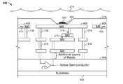
- FIG. 2is a diagram illustrating a cross-sectional view of an embodiment of a semiconductor device 200 with an integrated noise shield.
- semiconductor device 200is a nanopore device in a single cell of a nanopore array, and the integrated noise shield shields the nanopore device from both external noise sources and internal noise sources.
- the integrated noise shield disclosed hereincan also be integrated into other types of bio-sensor semiconductor arrays, such as bio-sensor semiconductor arrays in which low-level signal measurements susceptible to different noise sources are made.
- a nanopore deviceis used hereinafter as an example for semiconductor device 200 . However, a nanopore device is selected for illustration purposes only; accordingly, the present application is not limited to this specific example only.
- the integrated noise shieldsurrounds and shields the portions of semiconductor device 200 that are susceptible to different noise sources.
- the portions of semiconductor device 200 that are susceptible to noiseinclude a biological sample 202 , a measurement electrode 204 , other measurement integrated circuitries (not shown in the figure), and the like, and these portions of semiconductor device 200 are surrounded and shielded by the integrated noise shield.
- the integrated noise shieldcan be formed using any conductive material.
- the integrated noise shieldincludes a bottom shield.
- the bottom shieldincludes one or more conductive layers ( 206 A and 206 B) that are placed below the portions of semiconductor device 200 that are susceptible to noise.
- conductive layer 206 Ais metal layer 5 (M 5 ), which is the metal layer below the top metal layer 208 (M 6 ) of semiconductor device 200 .
- Conductive layer 206 Bis metal layer 5 ′(M 5 ′ or MIM Cap layer), which is a metal layer sitting on top of M 5 with a thin layer of oxide 210 in between.
- the bottom shieldis formed using conductive materials other than metal, including polycrystalline silicon, and the like.
- semiconductor device 200includes other conductive layers, such as a layer of substrate. Since the layer of substrate is typically thick and conductive, it acts as a bottom shield layer for semiconductor device 200 .
- the integrated noise shieldincludes a top shield.
- the top shieldincludes a conductive layer 208 with an opening 212 .
- the conductive layer 208 of the top shieldis a metal layer placed above the portions of semiconductor device 200 that are susceptible to noise.
- conductive layer 208is metal layer 6 (M 6 ), which is the top metal layer of semiconductor device 200 .
- opening 212allows biological sample 202 to be introduced into semiconductor device 200 such that biological sample 202 can be tested or analyzed by semiconductor device 200 .
- the top shieldfurther includes a conductive liquid shield 214 deposited over and covering the portions of semiconductor device 200 that are susceptible to noise, including biological sample 202 . Without conductive liquid shield 214 , opening 212 would expose semiconductor device 200 to different noise sources. In addition, conductive layer 208 (e.g., M 6 ) cannot come into contact with the conductive liquid shield 214 . Therefore, conductive layer 208 is covered with a layer of oxide 216 to insulate it from conductive liquid shield 214 . In some embodiments, conductive liquid shield 214 is an electrolyte containing free ions that make the electrolyte electrically conductive.
- the integrated noise shieldfurther includes a side shield.
- the side shieldincludes a plurality of vertical shielding structures 218 forming a sidewall substantially surrounding the noise sensitive portions of semiconductor device 200 . Note that in FIG. 2 , only two vertical shielding structures 218 are illustrated. However, the number of vertical shielding structures 218 can be more than two as well.
- vertical shielding structures 218include vias. Vias are formed by etching holes in insulating materials and depositing tungsten or other conductive material in the etched holes. The vias are used to make vertical conductive connections between the various metal or other conductive layers of semiconductor device 200 . For example, with reference to FIG. 2 , vias 218 interconnect conductive layer 208 and conductive layer 206 A.
- the plurality of vertical shielding structures 218can be arranged in different configurations to achieve maximum shielding.
- FIG. 3Ais a diagram illustrating a top-view of an exemplary configuration of vertical shielding structures 218 .
- the plurality of vertical shielding structures 218e.g., vias
- the plurality of vertical shielding structures 218can be arranged in a rectangular layout surrounding measurement electrode 204 and other noise sensitive portions of semiconductor device 200 .
- other configuration shapescan be used as well.
- the plurality of vertical shielding structures 218can be arranged in a concentric ring surrounding measurement electrode 204 and other noise sensitive portions of semiconductor device 200 .
- FIG. 3Bis a second diagram illustrating a top-view of another exemplary configuration of vertical shielding structures 218 .
- the plurality of vertical shielding structures 218are arranged in a plurality of concentric squares or rings, e.g., two concentric squares.
- the vertical shielding structures 218 in one ringare offset from the vertical shielding structures 218 in a different ring, i.e., the rings of vertical shielding structures 218 are not aligned together.
- a single continuous shielding wall surrounding the noise sensitive portions of semiconductor device 200may provide good shielding, the implementation of such a shielding wall may not be feasible due to various design or technical constraints.
- the shielding effectis close to that achieved by forming a single continuous shielding wall surrounding the noise sensitive portions of semiconductor device 200 .
- conductive layer 208which is a portion of the top shield, can be extended horizontally and radially outwards in the directions indicated by arrows 218 and 220 , respectively. Extending conductive layer 208 outwardly in this manner creates a roof edge or awning shielding, which can further prevent some of the interference from passing through a plurality of gaps between the plurality of vertical shielding structures 218 .
- the amount of extension of conductive layer 208 described abovecan be traded off against the density of the plurality of vertical shielding structures 218 .
- Viasare typically made of tungsten, and polishing tungsten becomes more challenging when the vias are more densely populated. Therefore, in some embodiments, the plurality of vertical shielding structures 218 can be spaced further apart when conductive layer 208 is extended further outward to form an expanded roof edge or awning to prevent some of the interference from infiltrating in between the plurality of vertical shielding structures 218 .
- some of the conductive layers or oxide layers forming the integrated shield of semiconductor device 200are exploited to form a capacitor.
- the oxide layer 210 between M 5 ′ and M 5forms a capacitor 222 .
- semiconductor device 200requires capacitors for various purposes.
- the integrating amplifier in semiconductor device 200may require a capacitance, which can be provided by capacitor 222 .
- FIG. 4is a diagram illustrating a cross-sectional view of an embodiment of a semiconductor device 400 with an integrated noise shield.
- the integrated noise shieldsurrounds and shields the portions of semiconductor device 400 that are susceptible to different noise sources.
- the integrated noise shieldincludes a bottom shield.
- the bottom shieldincludes a substrate layer 402 that is placed below the portions of semiconductor device 400 that are susceptible to noise, including a layer 404 containing active semiconductor circuits.
- the integrated noise shieldincludes a top shield.
- the top shieldincludes a conductive liquid shield 214 deposited over and covering the portions of semiconductor device 400 that are susceptible to noise, including biological sample 202 .
- Conductive layer 406e.g., M 6
- conductive layer 406is covered with a layer of oxide 216 to insulate it from conductive liquid shield 214 , which may be an aqueous electrolyte solution as described earlier.
- the integrated noise shieldfurther includes a side shield.
- the side shieldincludes a plurality of vertical shielding structures 218 (e.g., vias) forming a sidewall substantially surrounding the noise sensitive portions of semiconductor device 400 .
- the plurality of vertical shielding structures 218can be arranged in different configurations to achieve maximum shielding. For example, configurations similar to those in FIG. 3A and FIG. 3B may be used.
- conductive layer 406can be extended radially outwards in the directions indicated by arrows 408 and 410 , respectively. Extending conductive layer 406 outwards in this manner creates a roof edge or awning, which can prevent some of the interference from infiltrating in between the plurality of vertical shielding structures 218 . In some embodiments, the amount of extension of conductive layer 406 described above can be traded off against the density of the plurality of vertical shielding structures 218 .
Landscapes
- Health & Medical Sciences (AREA)
- Engineering & Computer Science (AREA)
- Life Sciences & Earth Sciences (AREA)
- Physics & Mathematics (AREA)
- Chemical & Material Sciences (AREA)
- General Physics & Mathematics (AREA)
- Molecular Biology (AREA)
- Biomedical Technology (AREA)
- Condensed Matter Physics & Semiconductors (AREA)
- Microelectronics & Electronic Packaging (AREA)
- Computer Hardware Design (AREA)
- Power Engineering (AREA)
- General Health & Medical Sciences (AREA)
- Pathology (AREA)
- Immunology (AREA)
- Analytical Chemistry (AREA)
- Biochemistry (AREA)
- Chemical Kinetics & Catalysis (AREA)
- Electrochemistry (AREA)
- Manufacturing & Machinery (AREA)
- Dispersion Chemistry (AREA)
- Nanotechnology (AREA)
- Spectroscopy & Molecular Physics (AREA)
- Biophysics (AREA)
- Hematology (AREA)
- Urology & Nephrology (AREA)
- Food Science & Technology (AREA)
- Medicinal Chemistry (AREA)
- Toxicology (AREA)
- Electromagnetism (AREA)
- Investigating Or Analyzing Materials By The Use Of Electric Means (AREA)
- Shielding Devices Or Components To Electric Or Magnetic Fields (AREA)
Abstract
Description
Claims (22)
Priority Applications (11)
| Application Number | Priority Date | Filing Date | Title |
|---|---|---|---|
| US13/396,522US8541849B2 (en) | 2012-02-14 | 2012-02-14 | Noise shielding techniques for ultra low current measurements in biochemical applications |
| PCT/US2012/069911WO2013122672A1 (en) | 2012-02-14 | 2012-12-14 | Noise shielding techniques for ultra low current measurements in biochemical applications |
| CA2863318ACA2863318C (en) | 2012-02-14 | 2012-12-14 | Noise shielding techniques for ultra low current measurements in biochemical applications |
| EP12868506.2AEP2815425B1 (en) | 2012-02-14 | 2012-12-14 | Noise shielding techniques for ultra low current measurements in biochemical applications |
| CN201280069446.9ACN104160484B (en) | 2012-02-14 | 2012-12-14 | The RESEARCH ON Sound Insulation of extremely low current measurement in biochemistry is applied |
| JP2014556549AJP6141330B2 (en) | 2012-02-14 | 2012-12-14 | Noise shielding techniques for ultra-low current measurements in biochemical applications |
| US13/972,616US8928097B2 (en) | 2012-02-14 | 2013-08-21 | Noise shielding techniques for ultra low current measurements in biochemical applications |
| US14/558,222US9121826B2 (en) | 2012-02-14 | 2014-12-02 | Noise shielding techniques for ultra low current measurements in biochemical applications |
| US14/808,953US9490204B2 (en) | 2012-02-14 | 2015-07-24 | Noise shielding techniques for ultra low current measurements in biochemical applications |
| JP2015195729AJP2016036035A (en) | 2012-02-14 | 2015-10-01 | Noise shielding techniques for ultra-low current measurements in biochemical applications |
| US15/240,872US9806033B2 (en) | 2012-02-14 | 2016-08-18 | Noise shielding techniques for ultra low current measurements in biochemical applications |
Applications Claiming Priority (1)
| Application Number | Priority Date | Filing Date | Title |
|---|---|---|---|
| US13/396,522US8541849B2 (en) | 2012-02-14 | 2012-02-14 | Noise shielding techniques for ultra low current measurements in biochemical applications |
Related Child Applications (1)
| Application Number | Title | Priority Date | Filing Date |
|---|---|---|---|
| US13/972,616ContinuationUS8928097B2 (en) | 2012-02-14 | 2013-08-21 | Noise shielding techniques for ultra low current measurements in biochemical applications |
Publications (2)
| Publication Number | Publication Date |
|---|---|
| US20130207205A1 US20130207205A1 (en) | 2013-08-15 |
| US8541849B2true US8541849B2 (en) | 2013-09-24 |
Family
ID=48944920
Family Applications (5)
| Application Number | Title | Priority Date | Filing Date |
|---|---|---|---|
| US13/396,522ActiveUS8541849B2 (en) | 2012-02-14 | 2012-02-14 | Noise shielding techniques for ultra low current measurements in biochemical applications |
| US13/972,616Active2032-02-23US8928097B2 (en) | 2012-02-14 | 2013-08-21 | Noise shielding techniques for ultra low current measurements in biochemical applications |
| US14/558,222ActiveUS9121826B2 (en) | 2012-02-14 | 2014-12-02 | Noise shielding techniques for ultra low current measurements in biochemical applications |
| US14/808,953ActiveUS9490204B2 (en) | 2012-02-14 | 2015-07-24 | Noise shielding techniques for ultra low current measurements in biochemical applications |
| US15/240,872ActiveUS9806033B2 (en) | 2012-02-14 | 2016-08-18 | Noise shielding techniques for ultra low current measurements in biochemical applications |
Family Applications After (4)
| Application Number | Title | Priority Date | Filing Date |
|---|---|---|---|
| US13/972,616Active2032-02-23US8928097B2 (en) | 2012-02-14 | 2013-08-21 | Noise shielding techniques for ultra low current measurements in biochemical applications |
| US14/558,222ActiveUS9121826B2 (en) | 2012-02-14 | 2014-12-02 | Noise shielding techniques for ultra low current measurements in biochemical applications |
| US14/808,953ActiveUS9490204B2 (en) | 2012-02-14 | 2015-07-24 | Noise shielding techniques for ultra low current measurements in biochemical applications |
| US15/240,872ActiveUS9806033B2 (en) | 2012-02-14 | 2016-08-18 | Noise shielding techniques for ultra low current measurements in biochemical applications |
Country Status (6)
| Country | Link |
|---|---|
| US (5) | US8541849B2 (en) |
| EP (1) | EP2815425B1 (en) |
| JP (2) | JP6141330B2 (en) |
| CN (1) | CN104160484B (en) |
| CA (1) | CA2863318C (en) |
| WO (1) | WO2013122672A1 (en) |
Cited By (12)
| Publication number | Priority date | Publication date | Assignee | Title |
|---|---|---|---|---|
| US8845880B2 (en) | 2010-12-22 | 2014-09-30 | Genia Technologies, Inc. | Nanopore-based single DNA molecule characterization, identification and isolation using speed bumps |
| US9322062B2 (en) | 2013-10-23 | 2016-04-26 | Genia Technologies, Inc. | Process for biosensor well formation |
| US9494554B2 (en) | 2012-06-15 | 2016-11-15 | Genia Technologies, Inc. | Chip set-up and high-accuracy nucleic acid sequencing |
| US9605309B2 (en) | 2012-11-09 | 2017-03-28 | Genia Technologies, Inc. | Nucleic acid sequencing using tags |
| US20170103952A1 (en)* | 2012-02-14 | 2017-04-13 | Genia Technologies, Inc. | Noise shielding techniques for ultra low current measurements in biochemical applications |
| US10190158B2 (en) | 2015-08-06 | 2019-01-29 | Pacific Biosciences Of California, Inc. | Systems and methods for selectively addressing sparsely arranged electronic measurement devices |
| US10240195B2 (en) | 2014-03-24 | 2019-03-26 | The Trustees Of Columbia University In The City Of New York | Chemical methods for producing tagged nucleotides |
| US10246479B2 (en) | 2012-04-09 | 2019-04-02 | The Trustees Of Columbia University In The City Of New York | Method of preparation of nanopore and uses thereof |
| US10421995B2 (en) | 2013-10-23 | 2019-09-24 | Genia Technologies, Inc. | High speed molecular sensing with nanopores |
| US10443096B2 (en) | 2010-12-17 | 2019-10-15 | The Trustees Of Columbia University In The City Of New York | DNA sequencing by synthesis using modified nucleotides and nanopore detection |
| US10732183B2 (en) | 2013-03-15 | 2020-08-04 | The Trustees Of Columbia University In The City Of New York | Method for detecting multiple predetermined compounds in a sample |
| US11608523B2 (en) | 2012-06-20 | 2023-03-21 | The Trustees Of Columbia University In The City Of New York | Nucleic acid sequencing by nanopore detection of tag molecules |
Families Citing this family (20)
| Publication number | Priority date | Publication date | Assignee | Title |
|---|---|---|---|---|
| GB0724736D0 (en) | 2007-12-19 | 2008-01-30 | Oxford Nanolabs Ltd | Formation of layers of amphiphilic molecules |
| US9678055B2 (en) | 2010-02-08 | 2017-06-13 | Genia Technologies, Inc. | Methods for forming a nanopore in a lipid bilayer |
| US9605307B2 (en) | 2010-02-08 | 2017-03-28 | Genia Technologies, Inc. | Systems and methods for forming a nanopore in a lipid bilayer |
| US8324914B2 (en) | 2010-02-08 | 2012-12-04 | Genia Technologies, Inc. | Systems and methods for characterizing a molecule |
| US8962242B2 (en) | 2011-01-24 | 2015-02-24 | Genia Technologies, Inc. | System for detecting electrical properties of a molecular complex |
| US9110478B2 (en) | 2011-01-27 | 2015-08-18 | Genia Technologies, Inc. | Temperature regulation of measurement arrays |
| GB201202519D0 (en) | 2012-02-13 | 2012-03-28 | Oxford Nanopore Tech Ltd | Apparatus for supporting an array of layers of amphiphilic molecules and method of forming an array of layers of amphiphilic molecules |
| US8986629B2 (en) | 2012-02-27 | 2015-03-24 | Genia Technologies, Inc. | Sensor circuit for controlling, detecting, and measuring a molecular complex |
| GB201313121D0 (en) | 2013-07-23 | 2013-09-04 | Oxford Nanopore Tech Ltd | Array of volumes of polar medium |
| US9759711B2 (en) | 2013-02-05 | 2017-09-12 | Genia Technologies, Inc. | Nanopore arrays |
| US9551697B2 (en) | 2013-10-17 | 2017-01-24 | Genia Technologies, Inc. | Non-faradaic, capacitively coupled measurement in a nanopore cell array |
| US10006899B2 (en)* | 2014-03-25 | 2018-06-26 | Genia Technologies, Inc. | Nanopore-based sequencing chips using stacked wafer technology |
| GB201611770D0 (en) | 2016-07-06 | 2016-08-17 | Oxford Nanopore Tech | Microfluidic device |
| GB2568895B (en) | 2017-11-29 | 2021-10-27 | Oxford Nanopore Tech Ltd | Microfluidic device |
| CN113574381B (en) | 2019-03-12 | 2025-08-26 | 牛津纳米孔科技公开有限公司 | Nanopore sensing devices, components, and operating methods |
| CN115989410A (en) | 2020-07-17 | 2023-04-18 | 牛津纳米孔科技公开有限公司 | Nanopore Sensing Device |
| US11940404B2 (en) | 2022-02-16 | 2024-03-26 | Western Digital Technologies, Inc. | Low noise amplifiers with shields for nanopore Applications |
| US11946894B2 (en) | 2022-02-16 | 2024-04-02 | Western Digital Technologies, Inc. | Low noise amplifiers with feedback for nanopore applications |
| US12259353B2 (en) | 2022-04-19 | 2025-03-25 | Western Digital Technologies, Inc. | Amplifiers for biological sensing applications |
| CN115135000A (en)* | 2022-08-09 | 2022-09-30 | 生益电子股份有限公司 | Printed circuit board and method of making the same |
Citations (14)
| Publication number | Priority date | Publication date | Assignee | Title |
|---|---|---|---|---|
| US5869244A (en) | 1994-07-07 | 1999-02-09 | Martin; Jean-Rene | Procedure for the analysis of biological substances in a conductive liquid medium |
| US6485703B1 (en)* | 1998-07-31 | 2002-11-26 | The Texas A&M University System | Compositions and methods for analyte detection |
| US20060278992A1 (en) | 2005-06-14 | 2006-12-14 | John Trezza | Post & penetration interconnection |
| US7368668B2 (en) | 2006-02-03 | 2008-05-06 | Freescale Semiconductor Inc. | Ground shields for semiconductors |
| US7446017B2 (en) | 2006-05-31 | 2008-11-04 | Freescale Semiconductor, Inc. | Methods and apparatus for RF shielding in vertically-integrated semiconductor devices |
| US20080318245A1 (en) | 2003-06-13 | 2008-12-25 | Smirnov Alex I | Nanotube structures having a surfactant bilayer inner wall coating |
| US20090066315A1 (en)* | 2005-10-21 | 2009-03-12 | The University Of Akron | Dynamic modulation for multiplexation of microfluidic and nanofluidic based biosensors |
| US7626379B2 (en) | 1997-06-06 | 2009-12-01 | Cascade Microtech, Inc. | Probe station having multiple enclosures |
| US20100025238A1 (en)* | 2008-07-31 | 2010-02-04 | Medtronic Minimed, Inc. | Analyte sensor apparatuses having improved electrode configurations and methods for making and using them |
| US20100072080A1 (en)* | 2008-05-05 | 2010-03-25 | The Regents Of The University Of California | Functionalized Nanopipette Biosensor |
| US20100078777A1 (en)* | 2008-09-30 | 2010-04-01 | Hans-Joachim Barth | On-Chip Radio Frequency Shield with Interconnect Metallization |
| US7906371B2 (en) | 2008-05-28 | 2011-03-15 | Stats Chippac, Ltd. | Semiconductor device and method of forming holes in substrate to interconnect top shield and ground shield |
| US7989928B2 (en) | 2008-02-05 | 2011-08-02 | Advanced Semiconductor Engineering Inc. | Semiconductor device packages with electromagnetic interference shielding |
| US8022511B2 (en)* | 2008-02-05 | 2011-09-20 | Advanced Semiconductor Engineering, Inc. | Semiconductor device packages with electromagnetic interference shielding |
Family Cites Families (19)
| Publication number | Priority date | Publication date | Assignee | Title |
|---|---|---|---|---|
| AT403528B (en)* | 1989-04-04 | 1998-03-25 | Urban Gerald | MICRO-MULTI-ELECTRODE STRUCTURE FOR ELECTROCHEMICAL APPLICATIONS AND METHOD FOR THEIR PRODUCTION |
| FR2795817B1 (en)* | 1999-07-02 | 2001-08-10 | Inst Francais Du Petrole | CAPACITIVE PROBE FOR MEASURING THE LEVEL OF AN ELECTRICALLY CONDUCTING LIQUID IN A CONTAINER AND METHOD FOR MANUFACTURING SUCH A PROBE |
| US20050009004A1 (en)* | 2002-05-04 | 2005-01-13 | Jia Xu | Apparatus including ion transport detecting structures and methods of use |
| US7361946B2 (en)* | 2004-06-28 | 2008-04-22 | Nitronex Corporation | Semiconductor device-based sensors |
| JP2006073991A (en)* | 2004-08-02 | 2006-03-16 | Sony Corp | Electromagnetic wave suppressing material, electromagnetic wave suppressing device and electronic equipment |
| JP2007047135A (en)* | 2005-08-05 | 2007-02-22 | Aomoriken Kogyo Gijutsu Kyoiku Shinkokai | Gel-like electrolyte for polarographic electrode and method for producing the same |
| US20080254995A1 (en)* | 2007-02-27 | 2008-10-16 | Drexel University | Nanopore arrays and sequencing devices and methods thereof |
| JP4927159B2 (en) | 2007-03-01 | 2012-05-09 | シャープ株式会社 | Display panel substrate, display panel, display device, and display panel substrate manufacturing method |
| JP5063500B2 (en) | 2008-02-08 | 2012-10-31 | 富士通コンポーネント株式会社 | Panel-type input device, method for manufacturing panel-type input device, and electronic apparatus including panel-type input device |
| KR100894710B1 (en) | 2008-06-27 | 2009-04-24 | (주) 월드비젼 | Window integrated touch screen and manufacturing method thereof |
| JP5369827B2 (en)* | 2009-03-31 | 2013-12-18 | Tdk株式会社 | Electronic component built-in module |
| EP2237027B1 (en)* | 2009-04-03 | 2011-11-30 | Nxp B.V. | Sensor device and a method of manufacturing the same |
| JP5189032B2 (en)* | 2009-06-16 | 2013-04-24 | 新光電気工業株式会社 | Semiconductor device and multilayer wiring board |
| KR101029490B1 (en) | 2009-07-20 | 2011-04-18 | (주) 월드비젼 | Window panel integrated capacitive touch sensor and manufacturing method thereof |
| EP4268944A3 (en)* | 2010-02-23 | 2024-03-20 | University of Washington | Analyte sequencing with nanopores |
| EP2492675B1 (en)* | 2011-02-28 | 2019-01-30 | Nxp B.V. | A biosensor chip and a method of manufacturing the same |
| US8541849B2 (en)* | 2012-02-14 | 2013-09-24 | Genia Technologies, Inc. | Noise shielding techniques for ultra low current measurements in biochemical applications |
| US9182369B2 (en)* | 2013-06-19 | 2015-11-10 | Globalfoundries Inc. | Manufacturable sub-3 nanometer palladium gap devices for fixed electrode tunneling recognition |
| US9188578B2 (en)* | 2013-06-19 | 2015-11-17 | Globalfoundries Inc. | Nanogap device with capped nanowire structures |
- 2012
- 2012-02-14USUS13/396,522patent/US8541849B2/enactiveActive
- 2012-12-14CACA2863318Apatent/CA2863318C/enactiveActive
- 2012-12-14JPJP2014556549Apatent/JP6141330B2/enactiveActive
- 2012-12-14WOPCT/US2012/069911patent/WO2013122672A1/enactiveApplication Filing
- 2012-12-14CNCN201280069446.9Apatent/CN104160484B/enactiveActive
- 2012-12-14EPEP12868506.2Apatent/EP2815425B1/enactiveActive
- 2013
- 2013-08-21USUS13/972,616patent/US8928097B2/enactiveActive
- 2014
- 2014-12-02USUS14/558,222patent/US9121826B2/enactiveActive
- 2015
- 2015-07-24USUS14/808,953patent/US9490204B2/enactiveActive
- 2015-10-01JPJP2015195729Apatent/JP2016036035A/enactivePending
- 2016
- 2016-08-18USUS15/240,872patent/US9806033B2/enactiveActive
Patent Citations (14)
| Publication number | Priority date | Publication date | Assignee | Title |
|---|---|---|---|---|
| US5869244A (en) | 1994-07-07 | 1999-02-09 | Martin; Jean-Rene | Procedure for the analysis of biological substances in a conductive liquid medium |
| US7626379B2 (en) | 1997-06-06 | 2009-12-01 | Cascade Microtech, Inc. | Probe station having multiple enclosures |
| US6485703B1 (en)* | 1998-07-31 | 2002-11-26 | The Texas A&M University System | Compositions and methods for analyte detection |
| US20080318245A1 (en) | 2003-06-13 | 2008-12-25 | Smirnov Alex I | Nanotube structures having a surfactant bilayer inner wall coating |
| US20060278992A1 (en) | 2005-06-14 | 2006-12-14 | John Trezza | Post & penetration interconnection |
| US20090066315A1 (en)* | 2005-10-21 | 2009-03-12 | The University Of Akron | Dynamic modulation for multiplexation of microfluidic and nanofluidic based biosensors |
| US7368668B2 (en) | 2006-02-03 | 2008-05-06 | Freescale Semiconductor Inc. | Ground shields for semiconductors |
| US7446017B2 (en) | 2006-05-31 | 2008-11-04 | Freescale Semiconductor, Inc. | Methods and apparatus for RF shielding in vertically-integrated semiconductor devices |
| US7989928B2 (en) | 2008-02-05 | 2011-08-02 | Advanced Semiconductor Engineering Inc. | Semiconductor device packages with electromagnetic interference shielding |
| US8022511B2 (en)* | 2008-02-05 | 2011-09-20 | Advanced Semiconductor Engineering, Inc. | Semiconductor device packages with electromagnetic interference shielding |
| US20100072080A1 (en)* | 2008-05-05 | 2010-03-25 | The Regents Of The University Of California | Functionalized Nanopipette Biosensor |
| US7906371B2 (en) | 2008-05-28 | 2011-03-15 | Stats Chippac, Ltd. | Semiconductor device and method of forming holes in substrate to interconnect top shield and ground shield |
| US20100025238A1 (en)* | 2008-07-31 | 2010-02-04 | Medtronic Minimed, Inc. | Analyte sensor apparatuses having improved electrode configurations and methods for making and using them |
| US20100078777A1 (en)* | 2008-09-30 | 2010-04-01 | Hans-Joachim Barth | On-Chip Radio Frequency Shield with Interconnect Metallization |
Cited By (27)
| Publication number | Priority date | Publication date | Assignee | Title |
|---|---|---|---|---|
| US10443096B2 (en) | 2010-12-17 | 2019-10-15 | The Trustees Of Columbia University In The City Of New York | DNA sequencing by synthesis using modified nucleotides and nanopore detection |
| US12173366B2 (en) | 2010-12-17 | 2024-12-24 | The Trustees Of Columbia University In The City Of New York | DNA sequencing by synthesis using modified nucleotides and nanopore detection |
| US11499186B2 (en) | 2010-12-17 | 2022-11-15 | The Trustees Of Columbia University In The City Of New York | DNA sequencing by synthesis using modified nucleotides and nanopore detection |
| US10400278B2 (en) | 2010-12-22 | 2019-09-03 | Genia Technologies, Inc. | Nanopore-based single DNA molecule characterization, identification and isolation using speed bumps |
| US8845880B2 (en) | 2010-12-22 | 2014-09-30 | Genia Technologies, Inc. | Nanopore-based single DNA molecule characterization, identification and isolation using speed bumps |
| US10920271B2 (en) | 2010-12-22 | 2021-02-16 | Roche Sequencing Solutions, Inc. | Nanopore-based single DNA molecule characterization, identification and isolation using speed bumps |
| US9617593B2 (en) | 2010-12-22 | 2017-04-11 | Genia Technologies, Inc. | Nanopore-based single DNA molecule characterization, identification and isolation using speed bumps |
| US9121059B2 (en) | 2010-12-22 | 2015-09-01 | Genia Technologies, Inc. | Nanopore-based single molecule characterization |
| US20170103952A1 (en)* | 2012-02-14 | 2017-04-13 | Genia Technologies, Inc. | Noise shielding techniques for ultra low current measurements in biochemical applications |
| US9806033B2 (en)* | 2012-02-14 | 2017-10-31 | Genia Technologies, Inc. | Noise shielding techniques for ultra low current measurements in biochemical applications |
| US11795191B2 (en) | 2012-04-09 | 2023-10-24 | The Trustees Of Columbia University In The City Of New York | Method of preparation of nanopore and uses thereof |
| US10246479B2 (en) | 2012-04-09 | 2019-04-02 | The Trustees Of Columbia University In The City Of New York | Method of preparation of nanopore and uses thereof |
| US9494554B2 (en) | 2012-06-15 | 2016-11-15 | Genia Technologies, Inc. | Chip set-up and high-accuracy nucleic acid sequencing |
| US11608523B2 (en) | 2012-06-20 | 2023-03-21 | The Trustees Of Columbia University In The City Of New York | Nucleic acid sequencing by nanopore detection of tag molecules |
| US11674174B2 (en) | 2012-11-09 | 2023-06-13 | The Trustees Of Columbia University In The City Of New York | Nucleic acid sequences using tags |
| US10526647B2 (en) | 2012-11-09 | 2020-01-07 | The Trustees Of Columbia University In The City Of New York | Nucleic acid sequences using tags |
| US10822650B2 (en) | 2012-11-09 | 2020-11-03 | Roche Sequencing Solutions, Inc. | Nucleic acid sequencing using tags |
| US9605309B2 (en) | 2012-11-09 | 2017-03-28 | Genia Technologies, Inc. | Nucleic acid sequencing using tags |
| US10732183B2 (en) | 2013-03-15 | 2020-08-04 | The Trustees Of Columbia University In The City Of New York | Method for detecting multiple predetermined compounds in a sample |
| US11021745B2 (en) | 2013-10-23 | 2021-06-01 | Roche Sequencing Solutions, Inc. | Methods for forming lipid bilayers on biochips |
| US9322062B2 (en) | 2013-10-23 | 2016-04-26 | Genia Technologies, Inc. | Process for biosensor well formation |
| US9567630B2 (en) | 2013-10-23 | 2017-02-14 | Genia Technologies, Inc. | Methods for forming lipid bilayers on biochips |
| US10421995B2 (en) | 2013-10-23 | 2019-09-24 | Genia Technologies, Inc. | High speed molecular sensing with nanopores |
| US11396677B2 (en) | 2014-03-24 | 2022-07-26 | The Trustees Of Columbia University In The City Of New York | Chemical methods for producing tagged nucleotides |
| US10240195B2 (en) | 2014-03-24 | 2019-03-26 | The Trustees Of Columbia University In The City Of New York | Chemical methods for producing tagged nucleotides |
| US11773437B2 (en) | 2015-08-06 | 2023-10-03 | Pacific Biosciences Of California, Inc. | Systems and methods for selectively addressing sparsely arranged electronic measurement devices |
| US10190158B2 (en) | 2015-08-06 | 2019-01-29 | Pacific Biosciences Of California, Inc. | Systems and methods for selectively addressing sparsely arranged electronic measurement devices |
Also Published As
| Publication number | Publication date |
|---|---|
| CA2863318C (en) | 2019-10-08 |
| CA2863318A1 (en) | 2013-08-22 |
| US20170103952A1 (en) | 2017-04-13 |
| US20140027866A1 (en) | 2014-01-30 |
| EP2815425B1 (en) | 2018-08-15 |
| US20160027728A1 (en) | 2016-01-28 |
| JP6141330B2 (en) | 2017-06-07 |
| US9121826B2 (en) | 2015-09-01 |
| US9490204B2 (en) | 2016-11-08 |
| US9806033B2 (en) | 2017-10-31 |
| WO2013122672A1 (en) | 2013-08-22 |
| EP2815425A1 (en) | 2014-12-24 |
| CN104160484B (en) | 2016-09-28 |
| US20150185185A1 (en) | 2015-07-02 |
| CN104160484A (en) | 2014-11-19 |
| EP2815425A4 (en) | 2015-10-21 |
| JP2016036035A (en) | 2016-03-17 |
| JP2015509658A (en) | 2015-03-30 |
| US20130207205A1 (en) | 2013-08-15 |
| US8928097B2 (en) | 2015-01-06 |
Similar Documents
| Publication | Publication Date | Title |
|---|---|---|
| US9806033B2 (en) | Noise shielding techniques for ultra low current measurements in biochemical applications | |
| US8821798B2 (en) | Titanium nitride as sensing layer for microwell structure | |
| Ganji et al. | Scaling effects on the electrochemical performance of poly (3, 4‐ethylenedioxythiophene (PEDOT), Au, and Pt for electrocorticography recording | |
| US11008611B2 (en) | Double gate ion sensitive field effect transistor | |
| Zhang et al. | High‐performance dopamine sensors based on whole‐graphene solution‐gated transistors | |
| US20170199151A1 (en) | System for communicating information from an array of sensors | |
| US20050227373A1 (en) | Method and device for high sensitivity detection of the presence of dna and other probes | |
| WO2004077041A1 (en) | Analytic chip for quantifying nucleic acid concentration, analytic device for quantifying nucleic acid concentration and analytic method for quantifying nucleic acid concentration | |
| US9891186B2 (en) | Method for analyzing analyte concentration in a liquid sample | |
| US20140026642A1 (en) | Capacitive sensor comprising differing unit cell structures | |
| US10920312B2 (en) | Electrochemical cell with increased current density | |
| Plačkić et al. | Electrochemistry at the Edge of a van der Waals Heterostructure | |
| US10908113B2 (en) | Liquid-sensing apparatus and method of manufacturing the same | |
| CN103698368B (en) | A kind of senser element, sensor and moisture sensor device | |
| Yakushenko et al. | On‐chip fast scan cyclic voltammetry for selective detection of redox active neurotransmitters | |
| US20190107507A1 (en) | Sensing device and biological detection method | |
| CN108279266B (en) | electrochemical detector | |
| US11774439B2 (en) | Integrated biochemical sensor and method of manufacturing the same | |
| CN104037105A (en) | Detection method for through silicon via insulation layer deposition process | |
| Blair et al. | Wafer level characterisation of microelectrodes for electrochemical sensing applications | |
| Xie et al. | An improved electrochemical biosensing device architecture with ultra-thin and surface-modified dielectric stacking structure |
Legal Events
| Date | Code | Title | Description |
|---|---|---|---|
| AS | Assignment | Owner name:GENIA TECHNOLOGIES, INC., CALIFORNIA Free format text:ASSIGNMENT OF ASSIGNORS INTEREST;ASSIGNOR:CHEN, ROGER;REEL/FRAME:027848/0890 Effective date:20120308 | |
| AS | Assignment | Owner name:GLENVIEW INSTITUTIONAL PARTNERS, L.P., NEW YORK Free format text:SECURITY AGREEMENT;ASSIGNOR:GENIA TECHNOLOGIES, INC.;REEL/FRAME:030423/0652 Effective date:20130515 Owner name:GLENVIEW OFFSHORE OPPORTUNITY MASTER FUND, LTD., N Free format text:SECURITY AGREEMENT;ASSIGNOR:GENIA TECHNOLOGIES, INC.;REEL/FRAME:030423/0652 Effective date:20130515 Owner name:LIFE TECHNOLOGIES CORPORATION, CALIFORNIA Free format text:SECURITY AGREEMENT;ASSIGNOR:GENIA TECHNOLOGIES, INC.;REEL/FRAME:030423/0652 Effective date:20130515 Owner name:GLENVIEW CAPITAL OPPORTUNITY FUND, LP, NEW YORK Free format text:SECURITY AGREEMENT;ASSIGNOR:GENIA TECHNOLOGIES, INC.;REEL/FRAME:030423/0652 Effective date:20130515 Owner name:GLENVIEW CAPITAL PARTNERS LP, NEW YORK Free format text:SECURITY AGREEMENT;ASSIGNOR:GENIA TECHNOLOGIES, INC.;REEL/FRAME:030423/0652 Effective date:20130515 Owner name:GLENVIEW CAPITAL MASTER FUND LTD, NEW YORK Free format text:SECURITY AGREEMENT;ASSIGNOR:GENIA TECHNOLOGIES, INC.;REEL/FRAME:030423/0652 Effective date:20130515 Owner name:DOBKIN, ROBERT, CALIFORNIA Free format text:SECURITY AGREEMENT;ASSIGNOR:GENIA TECHNOLOGIES, INC.;REEL/FRAME:030423/0652 Effective date:20130515 Owner name:SHERMAN, LEN, CALIFORNIA Free format text:SECURITY AGREEMENT;ASSIGNOR:GENIA TECHNOLOGIES, INC.;REEL/FRAME:030423/0652 Effective date:20130515 | |
| STCF | Information on status: patent grant | Free format text:PATENTED CASE | |
| AS | Assignment | Owner name:GLENVIEW CAPITAL OPPORTUNITY FUND, LP, NEW YORK Free format text:SECURITY AGREEMENT;ASSIGNOR:GENIA TECHNOLOGIES, INC.;REEL/FRAME:032161/0007 Effective date:20140131 Owner name:GLENVIEW INSTITUTIONAL PARTNERS, L.P., NEW YORK Free format text:SECURITY AGREEMENT;ASSIGNOR:GENIA TECHNOLOGIES, INC.;REEL/FRAME:032161/0007 Effective date:20140131 Owner name:GLENVIEW CAPITAL PARTNERS LP, NEW YORK Free format text:SECURITY AGREEMENT;ASSIGNOR:GENIA TECHNOLOGIES, INC.;REEL/FRAME:032161/0007 Effective date:20140131 Owner name:GLENVIEW CAPITAL MASTER FUND LTD., NEW YORK Free format text:SECURITY AGREEMENT;ASSIGNOR:GENIA TECHNOLOGIES, INC.;REEL/FRAME:032161/0007 Effective date:20140131 Owner name:GLENVIEW OFFSHORE OPPORTUNITY MASTER FUND, LTD., N Free format text:SECURITY AGREEMENT;ASSIGNOR:GENIA TECHNOLOGIES, INC.;REEL/FRAME:032161/0007 Effective date:20140131 | |
| AS | Assignment | Owner name:GENIA TECHNOLOGIES, INC, CALIFORNIA Free format text:RELEASE OF SECURITY INTEREST;ASSIGNORS:GLENVIEW CAPITAL PARTNERS, L.P.;GLENVIEW OFFSHORE OPPORTUNITY MASTER FUND, LTD;GLENVIEW CAPITAL OPPORTUNITY FUND, L.P.;AND OTHERS;REEL/FRAME:033083/0203 Effective date:20140529 Owner name:GENIA TECHNOLOGIES, INC, CALIFORNIA Free format text:RELEASE OF SECURITY INTEREST;ASSIGNORS:GLENVIEW CAPITAL PARTNERS, L.P.;GLENVIEW OFFSHORE OPPORTUNITY MASTER FUND, LTD.;GLENVIEW CAPITAL OPPORTUNITY FUND, L.P.;AND OTHERS;REEL/FRAME:033083/0170 Effective date:20140529 | |
| FPAY | Fee payment | Year of fee payment:4 | |
| MAFP | Maintenance fee payment | Free format text:PAYMENT OF MAINTENANCE FEE, 8TH YEAR, LARGE ENTITY (ORIGINAL EVENT CODE: M1552); ENTITY STATUS OF PATENT OWNER: LARGE ENTITY Year of fee payment:8 | |
| AS | Assignment | Owner name:ROCHE SEQUENCING SOLUTIONS, INC., CALIFORNIA Free format text:MERGER;ASSIGNOR:GENIA TECHNOLOGIES, INC.;REEL/FRAME:064999/0989 Effective date:20181213 | |
| MAFP | Maintenance fee payment | Free format text:PAYMENT OF MAINTENANCE FEE, 12TH YEAR, LARGE ENTITY (ORIGINAL EVENT CODE: M1553); ENTITY STATUS OF PATENT OWNER: LARGE ENTITY Year of fee payment:12 |