US8535976B2 - Method for fabricating chip package with die and substrate - Google Patents
Method for fabricating chip package with die and substrateDownload PDFInfo
- Publication number
- US8535976B2 US8535976B2US10/454,972US45497203AUS8535976B2US 8535976 B2US8535976 B2US 8535976B2US 45497203 AUS45497203 AUS 45497203AUS 8535976 B2US8535976 B2US 8535976B2
- Authority
- US
- United States
- Prior art keywords
- substrate
- forming
- die
- dies
- circuit layer
- Prior art date
- Legal status (The legal status is an assumption and is not a legal conclusion. Google has not performed a legal analysis and makes no representation as to the accuracy of the status listed.)
- Expired - Fee Related
Links
- 239000000758substrateSubstances0.000titleclaimsabstractdescription135
- 238000000034methodMethods0.000titleclaimsdescription79
- 239000000919ceramicSubstances0.000claimsabstractdescription109
- 229920000642polymerPolymers0.000claimsdescription16
- 238000005520cutting processMethods0.000claimsdescription10
- 229910000679solderInorganic materials0.000claimsdescription7
- 238000000227grindingMethods0.000claimsdescription6
- 239000004593EpoxySubstances0.000claimsdescription4
- 239000004642PolyimideSubstances0.000claimsdescription3
- UMIVXZPTRXBADB-UHFFFAOYSA-NbenzocyclobuteneChemical compoundC1=CC=C2CCC2=C1UMIVXZPTRXBADB-UHFFFAOYSA-N0.000claimsdescription3
- 239000010949copperSubstances0.000claimsdescription3
- 238000009713electroplatingMethods0.000claimsdescription3
- 238000005530etchingMethods0.000claimsdescription3
- 239000011521glassSubstances0.000claimsdescription3
- 238000004544sputter depositionMethods0.000claimsdescription3
- RYGMFSIKBFXOCR-UHFFFAOYSA-NCopperChemical compound[Cu]RYGMFSIKBFXOCR-UHFFFAOYSA-N0.000claimsdescription2
- 229910052802copperInorganic materials0.000claimsdescription2
- 238000005553drillingMethods0.000claimsdescription2
- 238000007772electroless platingMethods0.000claimsdescription2
- PCHJSUWPFVWCPO-UHFFFAOYSA-NgoldChemical compound[Au]PCHJSUWPFVWCPO-UHFFFAOYSA-N0.000claimsdescription2
- 239000010931goldSubstances0.000claimsdescription2
- 229910052737goldInorganic materials0.000claimsdescription2
- 229920001721polyimidePolymers0.000claims1
- 239000010409thin filmSubstances0.000abstractdescription34
- 229910052751metalInorganic materials0.000abstractdescription25
- 239000002184metalSubstances0.000abstractdescription25
- 238000004519manufacturing processMethods0.000abstractdescription19
- 239000010410layerSubstances0.000description196
- 238000011049fillingMethods0.000description28
- 238000010586diagramMethods0.000description21
- 230000015572biosynthetic processEffects0.000description18
- 239000004020conductorSubstances0.000description12
- 239000000463materialSubstances0.000description10
- 238000002161passivationMethods0.000description6
- 229910010293ceramic materialInorganic materials0.000description5
- 239000011810insulating materialSubstances0.000description5
- 238000004806packaging method and processMethods0.000description5
- 239000002356single layerSubstances0.000description4
- 230000008901benefitEffects0.000description3
- 239000003990capacitorSubstances0.000description3
- 230000002093peripheral effectEffects0.000description3
- 238000005245sinteringMethods0.000description3
- 230000000694effectsEffects0.000description2
- 238000005516engineering processMethods0.000description2
- 230000010354integrationEffects0.000description2
- 238000012986modificationMethods0.000description2
- 230000004048modificationEffects0.000description2
- 239000011368organic materialSubstances0.000description2
- TWNQGVIAIRXVLR-UHFFFAOYSA-Noxo(oxoalumanyloxy)alumaneChemical compoundO=[Al]O[Al]=OTWNQGVIAIRXVLR-UHFFFAOYSA-N0.000description2
- 238000001020plasma etchingMethods0.000description2
- 230000008054signal transmissionEffects0.000description2
- 229910000990Ni alloyInorganic materials0.000description1
- KGWWEXORQXHJJQ-UHFFFAOYSA-N[Fe].[Co].[Ni]Chemical compound[Fe].[Co].[Ni]KGWWEXORQXHJJQ-UHFFFAOYSA-N0.000description1
- 239000002390adhesive tapeSubstances0.000description1
- 230000005540biological transmissionEffects0.000description1
- 239000011248coating agentSubstances0.000description1
- 238000000576coating methodMethods0.000description1
- 230000003247decreasing effectEffects0.000description1
- 238000000151depositionMethods0.000description1
- 239000003989dielectric materialSubstances0.000description1
- 238000010292electrical insulationMethods0.000description1
- 239000003292glueSubstances0.000description1
- 238000000608laser ablationMethods0.000description1
- 238000003698laser cuttingMethods0.000description1
- 238000003754machiningMethods0.000description1
- 238000002844meltingMethods0.000description1
- 230000008018meltingEffects0.000description1
- 238000004377microelectronicMethods0.000description1
- 238000003801millingMethods0.000description1
- 229910052574oxide ceramicInorganic materials0.000description1
- 238000000059patterningMethods0.000description1
- 238000000206photolithographyMethods0.000description1
- 238000007639printingMethods0.000description1
- 229910052710siliconInorganic materials0.000description1
- 239000010703siliconSubstances0.000description1
- 239000002344surface layerSubstances0.000description1
Images


Classifications
- H—ELECTRICITY
- H01—ELECTRIC ELEMENTS
- H01L—SEMICONDUCTOR DEVICES NOT COVERED BY CLASS H10
- H01L23/00—Details of semiconductor or other solid state devices
- H01L23/48—Arrangements for conducting electric current to or from the solid state body in operation, e.g. leads, terminal arrangements ; Selection of materials therefor
- H01L23/488—Arrangements for conducting electric current to or from the solid state body in operation, e.g. leads, terminal arrangements ; Selection of materials therefor consisting of soldered or bonded constructions
- H01L23/498—Leads, i.e. metallisations or lead-frames on insulating substrates, e.g. chip carriers
- H01L23/49822—Multilayer substrates
- H—ELECTRICITY
- H01—ELECTRIC ELEMENTS
- H01L—SEMICONDUCTOR DEVICES NOT COVERED BY CLASS H10
- H01L24/00—Arrangements for connecting or disconnecting semiconductor or solid-state bodies; Methods or apparatus related thereto
- H01L24/80—Methods for connecting semiconductor or other solid state bodies using means for bonding being attached to, or being formed on, the surface to be connected
- H01L24/82—Methods for connecting semiconductor or other solid state bodies using means for bonding being attached to, or being formed on, the surface to be connected by forming build-up interconnects at chip-level, e.g. for high density interconnects [HDI]
- H—ELECTRICITY
- H01—ELECTRIC ELEMENTS
- H01L—SEMICONDUCTOR DEVICES NOT COVERED BY CLASS H10
- H01L23/00—Details of semiconductor or other solid state devices
- H01L23/48—Arrangements for conducting electric current to or from the solid state body in operation, e.g. leads, terminal arrangements ; Selection of materials therefor
- H01L23/488—Arrangements for conducting electric current to or from the solid state body in operation, e.g. leads, terminal arrangements ; Selection of materials therefor consisting of soldered or bonded constructions
- H01L23/498—Leads, i.e. metallisations or lead-frames on insulating substrates, e.g. chip carriers
- H01L23/49866—Leads, i.e. metallisations or lead-frames on insulating substrates, e.g. chip carriers characterised by the materials
- H01L23/49894—Materials of the insulating layers or coatings
- H—ELECTRICITY
- H01—ELECTRIC ELEMENTS
- H01L—SEMICONDUCTOR DEVICES NOT COVERED BY CLASS H10
- H01L23/00—Details of semiconductor or other solid state devices
- H01L23/52—Arrangements for conducting electric current within the device in operation from one component to another, i.e. interconnections, e.g. wires, lead frames
- H01L23/538—Arrangements for conducting electric current within the device in operation from one component to another, i.e. interconnections, e.g. wires, lead frames the interconnection structure between a plurality of semiconductor chips being formed on, or in, insulating substrates
- H01L23/5389—Arrangements for conducting electric current within the device in operation from one component to another, i.e. interconnections, e.g. wires, lead frames the interconnection structure between a plurality of semiconductor chips being formed on, or in, insulating substrates the chips being integrally enclosed by the interconnect and support structures
- H—ELECTRICITY
- H01—ELECTRIC ELEMENTS
- H01L—SEMICONDUCTOR DEVICES NOT COVERED BY CLASS H10
- H01L24/00—Arrangements for connecting or disconnecting semiconductor or solid-state bodies; Methods or apparatus related thereto
- H01L24/01—Means for bonding being attached to, or being formed on, the surface to be connected, e.g. chip-to-package, die-attach, "first-level" interconnects; Manufacturing methods related thereto
- H01L24/18—High density interconnect [HDI] connectors; Manufacturing methods related thereto
- H01L24/19—Manufacturing methods of high density interconnect preforms
- H—ELECTRICITY
- H01—ELECTRIC ELEMENTS
- H01L—SEMICONDUCTOR DEVICES NOT COVERED BY CLASS H10
- H01L24/00—Arrangements for connecting or disconnecting semiconductor or solid-state bodies; Methods or apparatus related thereto
- H01L24/93—Batch processes
- H01L24/95—Batch processes at chip-level, i.e. with connecting carried out on a plurality of singulated devices, i.e. on diced chips
- H01L24/97—Batch processes at chip-level, i.e. with connecting carried out on a plurality of singulated devices, i.e. on diced chips the devices being connected to a common substrate, e.g. interposer, said common substrate being separable into individual assemblies after connecting
- H—ELECTRICITY
- H01—ELECTRIC ELEMENTS
- H01L—SEMICONDUCTOR DEVICES NOT COVERED BY CLASS H10
- H01L21/00—Processes or apparatus adapted for the manufacture or treatment of semiconductor or solid state devices or of parts thereof
- H01L21/02—Manufacture or treatment of semiconductor devices or of parts thereof
- H01L21/04—Manufacture or treatment of semiconductor devices or of parts thereof the devices having potential barriers, e.g. a PN junction, depletion layer or carrier concentration layer
- H01L21/50—Assembly of semiconductor devices using processes or apparatus not provided for in a single one of the groups H01L21/18 - H01L21/326 or H10D48/04 - H10D48/07 e.g. sealing of a cap to a base of a container
- H01L21/56—Encapsulations, e.g. encapsulation layers, coatings
- H01L21/568—Temporary substrate used as encapsulation process aid
- H—ELECTRICITY
- H01—ELECTRIC ELEMENTS
- H01L—SEMICONDUCTOR DEVICES NOT COVERED BY CLASS H10
- H01L2221/00—Processes or apparatus adapted for the manufacture or treatment of semiconductor or solid state devices or of parts thereof covered by H01L21/00
- H01L2221/67—Apparatus for handling semiconductor or electric solid state devices during manufacture or treatment thereof; Apparatus for handling wafers during manufacture or treatment of semiconductor or electric solid state devices or components; Apparatus not specifically provided for elsewhere
- H01L2221/683—Apparatus for handling semiconductor or electric solid state devices during manufacture or treatment thereof; Apparatus for handling wafers during manufacture or treatment of semiconductor or electric solid state devices or components; Apparatus not specifically provided for elsewhere for supporting or gripping
- H01L2221/68304—Apparatus for handling semiconductor or electric solid state devices during manufacture or treatment thereof; Apparatus for handling wafers during manufacture or treatment of semiconductor or electric solid state devices or components; Apparatus not specifically provided for elsewhere for supporting or gripping using temporarily an auxiliary support
- H01L2221/68377—Apparatus for handling semiconductor or electric solid state devices during manufacture or treatment thereof; Apparatus for handling wafers during manufacture or treatment of semiconductor or electric solid state devices or components; Apparatus not specifically provided for elsewhere for supporting or gripping using temporarily an auxiliary support with parts of the auxiliary support remaining in the finished device
- H—ELECTRICITY
- H01—ELECTRIC ELEMENTS
- H01L—SEMICONDUCTOR DEVICES NOT COVERED BY CLASS H10
- H01L2224/00—Indexing scheme for arrangements for connecting or disconnecting semiconductor or solid-state bodies and methods related thereto as covered by H01L24/00
- H01L2224/01—Means for bonding being attached to, or being formed on, the surface to be connected, e.g. chip-to-package, die-attach, "first-level" interconnects; Manufacturing methods related thereto
- H01L2224/02—Bonding areas; Manufacturing methods related thereto
- H01L2224/04—Structure, shape, material or disposition of the bonding areas prior to the connecting process
- H01L2224/0401—Bonding areas specifically adapted for bump connectors, e.g. under bump metallisation [UBM]
- H—ELECTRICITY
- H01—ELECTRIC ELEMENTS
- H01L—SEMICONDUCTOR DEVICES NOT COVERED BY CLASS H10
- H01L2224/00—Indexing scheme for arrangements for connecting or disconnecting semiconductor or solid-state bodies and methods related thereto as covered by H01L24/00
- H01L2224/01—Means for bonding being attached to, or being formed on, the surface to be connected, e.g. chip-to-package, die-attach, "first-level" interconnects; Manufacturing methods related thereto
- H01L2224/02—Bonding areas; Manufacturing methods related thereto
- H01L2224/04—Structure, shape, material or disposition of the bonding areas prior to the connecting process
- H01L2224/04105—Bonding areas formed on an encapsulation of the semiconductor or solid-state body, e.g. bonding areas on chip-scale packages
- H—ELECTRICITY
- H01—ELECTRIC ELEMENTS
- H01L—SEMICONDUCTOR DEVICES NOT COVERED BY CLASS H10
- H01L2224/00—Indexing scheme for arrangements for connecting or disconnecting semiconductor or solid-state bodies and methods related thereto as covered by H01L24/00
- H01L2224/01—Means for bonding being attached to, or being formed on, the surface to be connected, e.g. chip-to-package, die-attach, "first-level" interconnects; Manufacturing methods related thereto
- H01L2224/10—Bump connectors; Manufacturing methods related thereto
- H01L2224/12—Structure, shape, material or disposition of the bump connectors prior to the connecting process
- H01L2224/12105—Bump connectors formed on an encapsulation of the semiconductor or solid-state body, e.g. bumps on chip-scale packages
- H—ELECTRICITY
- H01—ELECTRIC ELEMENTS
- H01L—SEMICONDUCTOR DEVICES NOT COVERED BY CLASS H10
- H01L2224/00—Indexing scheme for arrangements for connecting or disconnecting semiconductor or solid-state bodies and methods related thereto as covered by H01L24/00
- H01L2224/01—Means for bonding being attached to, or being formed on, the surface to be connected, e.g. chip-to-package, die-attach, "first-level" interconnects; Manufacturing methods related thereto
- H01L2224/10—Bump connectors; Manufacturing methods related thereto
- H01L2224/12—Structure, shape, material or disposition of the bump connectors prior to the connecting process
- H01L2224/13—Structure, shape, material or disposition of the bump connectors prior to the connecting process of an individual bump connector
- H01L2224/13001—Core members of the bump connector
- H01L2224/1302—Disposition
- H01L2224/13022—Disposition the bump connector being at least partially embedded in the surface
- H—ELECTRICITY
- H01—ELECTRIC ELEMENTS
- H01L—SEMICONDUCTOR DEVICES NOT COVERED BY CLASS H10
- H01L2224/00—Indexing scheme for arrangements for connecting or disconnecting semiconductor or solid-state bodies and methods related thereto as covered by H01L24/00
- H01L2224/01—Means for bonding being attached to, or being formed on, the surface to be connected, e.g. chip-to-package, die-attach, "first-level" interconnects; Manufacturing methods related thereto
- H01L2224/18—High density interconnect [HDI] connectors; Manufacturing methods related thereto
- H01L2224/20—Structure, shape, material or disposition of high density interconnect preforms
- H01L2224/21—Structure, shape, material or disposition of high density interconnect preforms of an individual HDI interconnect
- H01L2224/211—Disposition
- H—ELECTRICITY
- H01—ELECTRIC ELEMENTS
- H01L—SEMICONDUCTOR DEVICES NOT COVERED BY CLASS H10
- H01L2224/00—Indexing scheme for arrangements for connecting or disconnecting semiconductor or solid-state bodies and methods related thereto as covered by H01L24/00
- H01L2224/01—Means for bonding being attached to, or being formed on, the surface to be connected, e.g. chip-to-package, die-attach, "first-level" interconnects; Manufacturing methods related thereto
- H01L2224/18—High density interconnect [HDI] connectors; Manufacturing methods related thereto
- H01L2224/23—Structure, shape, material or disposition of the high density interconnect connectors after the connecting process
- H01L2224/24—Structure, shape, material or disposition of the high density interconnect connectors after the connecting process of an individual high density interconnect connector
- H01L2224/241—Disposition
- H01L2224/24135—Connecting between different semiconductor or solid-state bodies, i.e. chip-to-chip
- H01L2224/24137—Connecting between different semiconductor or solid-state bodies, i.e. chip-to-chip the bodies being arranged next to each other, e.g. on a common substrate
- H—ELECTRICITY
- H01—ELECTRIC ELEMENTS
- H01L—SEMICONDUCTOR DEVICES NOT COVERED BY CLASS H10
- H01L2224/00—Indexing scheme for arrangements for connecting or disconnecting semiconductor or solid-state bodies and methods related thereto as covered by H01L24/00
- H01L2224/73—Means for bonding being of different types provided for in two or more of groups H01L2224/10, H01L2224/18, H01L2224/26, H01L2224/34, H01L2224/42, H01L2224/50, H01L2224/63, H01L2224/71
- H01L2224/732—Location after the connecting process
- H01L2224/73251—Location after the connecting process on different surfaces
- H01L2224/73267—Layer and HDI connectors
- H—ELECTRICITY
- H01—ELECTRIC ELEMENTS
- H01L—SEMICONDUCTOR DEVICES NOT COVERED BY CLASS H10
- H01L2224/00—Indexing scheme for arrangements for connecting or disconnecting semiconductor or solid-state bodies and methods related thereto as covered by H01L24/00
- H01L2224/93—Batch processes
- H01L2224/95—Batch processes at chip-level, i.e. with connecting carried out on a plurality of singulated devices, i.e. on diced chips
- H01L2224/97—Batch processes at chip-level, i.e. with connecting carried out on a plurality of singulated devices, i.e. on diced chips the devices being connected to a common substrate, e.g. interposer, said common substrate being separable into individual assemblies after connecting
- H—ELECTRICITY
- H01—ELECTRIC ELEMENTS
- H01L—SEMICONDUCTOR DEVICES NOT COVERED BY CLASS H10
- H01L2924/00—Indexing scheme for arrangements or methods for connecting or disconnecting semiconductor or solid-state bodies as covered by H01L24/00
- H01L2924/01—Chemical elements
- H01L2924/01005—Boron [B]
- H—ELECTRICITY
- H01—ELECTRIC ELEMENTS
- H01L—SEMICONDUCTOR DEVICES NOT COVERED BY CLASS H10
- H01L2924/00—Indexing scheme for arrangements or methods for connecting or disconnecting semiconductor or solid-state bodies as covered by H01L24/00
- H01L2924/01—Chemical elements
- H01L2924/01006—Carbon [C]
- H—ELECTRICITY
- H01—ELECTRIC ELEMENTS
- H01L—SEMICONDUCTOR DEVICES NOT COVERED BY CLASS H10
- H01L2924/00—Indexing scheme for arrangements or methods for connecting or disconnecting semiconductor or solid-state bodies as covered by H01L24/00
- H01L2924/01—Chemical elements
- H01L2924/01013—Aluminum [Al]
- H—ELECTRICITY
- H01—ELECTRIC ELEMENTS
- H01L—SEMICONDUCTOR DEVICES NOT COVERED BY CLASS H10
- H01L2924/00—Indexing scheme for arrangements or methods for connecting or disconnecting semiconductor or solid-state bodies as covered by H01L24/00
- H01L2924/01—Chemical elements
- H01L2924/01027—Cobalt [Co]
- H—ELECTRICITY
- H01—ELECTRIC ELEMENTS
- H01L—SEMICONDUCTOR DEVICES NOT COVERED BY CLASS H10
- H01L2924/00—Indexing scheme for arrangements or methods for connecting or disconnecting semiconductor or solid-state bodies as covered by H01L24/00
- H01L2924/01—Chemical elements
- H01L2924/01029—Copper [Cu]
- H—ELECTRICITY
- H01—ELECTRIC ELEMENTS
- H01L—SEMICONDUCTOR DEVICES NOT COVERED BY CLASS H10
- H01L2924/00—Indexing scheme for arrangements or methods for connecting or disconnecting semiconductor or solid-state bodies as covered by H01L24/00
- H01L2924/01—Chemical elements
- H01L2924/01033—Arsenic [As]
- H—ELECTRICITY
- H01—ELECTRIC ELEMENTS
- H01L—SEMICONDUCTOR DEVICES NOT COVERED BY CLASS H10
- H01L2924/00—Indexing scheme for arrangements or methods for connecting or disconnecting semiconductor or solid-state bodies as covered by H01L24/00
- H01L2924/01—Chemical elements
- H01L2924/01078—Platinum [Pt]
- H—ELECTRICITY
- H01—ELECTRIC ELEMENTS
- H01L—SEMICONDUCTOR DEVICES NOT COVERED BY CLASS H10
- H01L2924/00—Indexing scheme for arrangements or methods for connecting or disconnecting semiconductor or solid-state bodies as covered by H01L24/00
- H01L2924/01—Chemical elements
- H01L2924/01079—Gold [Au]
- H—ELECTRICITY
- H01—ELECTRIC ELEMENTS
- H01L—SEMICONDUCTOR DEVICES NOT COVERED BY CLASS H10
- H01L2924/00—Indexing scheme for arrangements or methods for connecting or disconnecting semiconductor or solid-state bodies as covered by H01L24/00
- H01L2924/095—Indexing scheme for arrangements or methods for connecting or disconnecting semiconductor or solid-state bodies as covered by H01L24/00 with a principal constituent of the material being a combination of two or more materials provided in the groups H01L2924/013 - H01L2924/0715
- H01L2924/097—Glass-ceramics, e.g. devitrified glass
- H01L2924/09701—Low temperature co-fired ceramic [LTCC]
- H—ELECTRICITY
- H01—ELECTRIC ELEMENTS
- H01L—SEMICONDUCTOR DEVICES NOT COVERED BY CLASS H10
- H01L2924/00—Indexing scheme for arrangements or methods for connecting or disconnecting semiconductor or solid-state bodies as covered by H01L24/00
- H01L2924/10—Details of semiconductor or other solid state devices to be connected
- H01L2924/11—Device type
- H01L2924/12—Passive devices, e.g. 2 terminal devices
- H01L2924/1204—Optical Diode
- H01L2924/12042—LASER
- H—ELECTRICITY
- H01—ELECTRIC ELEMENTS
- H01L—SEMICONDUCTOR DEVICES NOT COVERED BY CLASS H10
- H01L2924/00—Indexing scheme for arrangements or methods for connecting or disconnecting semiconductor or solid-state bodies as covered by H01L24/00
- H01L2924/10—Details of semiconductor or other solid state devices to be connected
- H01L2924/11—Device type
- H01L2924/14—Integrated circuits
- H—ELECTRICITY
- H01—ELECTRIC ELEMENTS
- H01L—SEMICONDUCTOR DEVICES NOT COVERED BY CLASS H10
- H01L2924/00—Indexing scheme for arrangements or methods for connecting or disconnecting semiconductor or solid-state bodies as covered by H01L24/00
- H01L2924/10—Details of semiconductor or other solid state devices to be connected
- H01L2924/146—Mixed devices
- H01L2924/1461—MEMS
- H—ELECTRICITY
- H01—ELECTRIC ELEMENTS
- H01L—SEMICONDUCTOR DEVICES NOT COVERED BY CLASS H10
- H01L2924/00—Indexing scheme for arrangements or methods for connecting or disconnecting semiconductor or solid-state bodies as covered by H01L24/00
- H01L2924/15—Details of package parts other than the semiconductor or other solid state devices to be connected
- H01L2924/151—Die mounting substrate
- H01L2924/1515—Shape
- H01L2924/15153—Shape the die mounting substrate comprising a recess for hosting the device
- H—ELECTRICITY
- H01—ELECTRIC ELEMENTS
- H01L—SEMICONDUCTOR DEVICES NOT COVERED BY CLASS H10
- H01L2924/00—Indexing scheme for arrangements or methods for connecting or disconnecting semiconductor or solid-state bodies as covered by H01L24/00
- H01L2924/15—Details of package parts other than the semiconductor or other solid state devices to be connected
- H01L2924/151—Die mounting substrate
- H01L2924/1517—Multilayer substrate
- H01L2924/15172—Fan-out arrangement of the internal vias
- H01L2924/15174—Fan-out arrangement of the internal vias in different layers of the multilayer substrate
- H—ELECTRICITY
- H01—ELECTRIC ELEMENTS
- H01L—SEMICONDUCTOR DEVICES NOT COVERED BY CLASS H10
- H01L2924/00—Indexing scheme for arrangements or methods for connecting or disconnecting semiconductor or solid-state bodies as covered by H01L24/00
- H01L2924/15—Details of package parts other than the semiconductor or other solid state devices to be connected
- H01L2924/151—Die mounting substrate
- H01L2924/153—Connection portion
- H01L2924/1531—Connection portion the connection portion being formed only on the surface of the substrate opposite to the die mounting surface
- H01L2924/15311—Connection portion the connection portion being formed only on the surface of the substrate opposite to the die mounting surface being a ball array, e.g. BGA
- H—ELECTRICITY
- H01—ELECTRIC ELEMENTS
- H01L—SEMICONDUCTOR DEVICES NOT COVERED BY CLASS H10
- H01L2924/00—Indexing scheme for arrangements or methods for connecting or disconnecting semiconductor or solid-state bodies as covered by H01L24/00
- H01L2924/15—Details of package parts other than the semiconductor or other solid state devices to be connected
- H01L2924/151—Die mounting substrate
- H01L2924/156—Material
- H01L2924/15786—Material with a principal constituent of the material being a non metallic, non metalloid inorganic material
- H01L2924/15787—Ceramics, e.g. crystalline carbides, nitrides or oxides
- H—ELECTRICITY
- H01—ELECTRIC ELEMENTS
- H01L—SEMICONDUCTOR DEVICES NOT COVERED BY CLASS H10
- H01L2924/00—Indexing scheme for arrangements or methods for connecting or disconnecting semiconductor or solid-state bodies as covered by H01L24/00
- H01L2924/15—Details of package parts other than the semiconductor or other solid state devices to be connected
- H01L2924/151—Die mounting substrate
- H01L2924/156—Material
- H01L2924/15786—Material with a principal constituent of the material being a non metallic, non metalloid inorganic material
- H01L2924/15788—Glasses, e.g. amorphous oxides, nitrides or fluorides
- H—ELECTRICITY
- H01—ELECTRIC ELEMENTS
- H01L—SEMICONDUCTOR DEVICES NOT COVERED BY CLASS H10
- H01L2924/00—Indexing scheme for arrangements or methods for connecting or disconnecting semiconductor or solid-state bodies as covered by H01L24/00
- H01L2924/19—Details of hybrid assemblies other than the semiconductor or other solid state devices to be connected
- H01L2924/1901—Structure
- H01L2924/1904—Component type
- H01L2924/19041—Component type being a capacitor
- H—ELECTRICITY
- H01—ELECTRIC ELEMENTS
- H01L—SEMICONDUCTOR DEVICES NOT COVERED BY CLASS H10
- H01L2924/00—Indexing scheme for arrangements or methods for connecting or disconnecting semiconductor or solid-state bodies as covered by H01L24/00
- H01L2924/19—Details of hybrid assemblies other than the semiconductor or other solid state devices to be connected
- H01L2924/1901—Structure
- H01L2924/1904—Component type
- H01L2924/19042—Component type being an inductor
- H—ELECTRICITY
- H01—ELECTRIC ELEMENTS
- H01L—SEMICONDUCTOR DEVICES NOT COVERED BY CLASS H10
- H01L2924/00—Indexing scheme for arrangements or methods for connecting or disconnecting semiconductor or solid-state bodies as covered by H01L24/00
- H01L2924/19—Details of hybrid assemblies other than the semiconductor or other solid state devices to be connected
- H01L2924/1901—Structure
- H01L2924/1904—Component type
- H01L2924/19043—Component type being a resistor
Definitions
- the present inventionrelates to an integrated chip package structure and method of manufacture the same. More particularly, the present invention relates to an integrated chip package structure and method of manufacture the same using ceramic substrate.
- the key componenthas to be the integrated circuit (IC) chip inside any electronic product.
- an IC chipThe operability, performance, and life of an IC chip are greatly affected by its circuit design, wafer manufacturing, and chip packaging.
- the focuswill be on chip packaging technique. Since the features and speed of IC chips are increasing rapidly, the need for increasing the conductivity of the circuitry is necessary so that the signal delay and attenuation of the dies to the external circuitry are reduced. A chip package that allows good thermal dissipation and protection of the IC chips with a small overall dimension of the package is also necessary for higher performance chips. These are the goals to be achieved in chip packaging.
- BGAball grid array
- wire bondingflip chip
- flip chipetc. . . .
- the inner traceshelps to fan out the bonding points on the bottom of the substrate.
- the solder ballsare separately planted on the bonding points for acting as an interface for the die to electrically connect to the external circuitry.
- pin grid arrayPGA is very much like BGA, which replaces the balls with pins on the substrate and PGA also acts an interface for the die to electrically connect to the external circuitry.
- Both BGA and PGA packagesrequire wiring or flip chip for mounting the die on the substrate.
- the inner traces in the substratefan out the bonding points on the substrate, and electrical connection to the external circuitry is carried out by the solder balls or pins on the bonding points.
- this methodfails to reduce the distance of the signal transmission path but in fact increase the signal path distance. This will increase signal delay and attenuation and decrease the performance of the chip.
- Wafer level chip scale packagehas an advantage of being able to print the redistribution circuit directly on the die by using the peripheral area of the die as the bonding points. It is achieved by redistributing an area array on the surface of the die, which can fully utilize the entire area of the die.
- the bonding pointsare located on the redistribution circuit by forming flip chip bumps so the bottom side of the die connects directly to the printed circuit board (PCB) with micro-spaced bonding points.
- WLCSPcan greatly reduce the signal path distance, it is still very difficult to accommodate all the bonding points on the die surface as the integration of die and internal devices gets higher.
- the pin count on the dieincreases as integration gets higher so the redistribution of pins in an area array is difficult to achieve. Even if the redistribution of pins is successful, the distance between pins will be too small to meet the pitch of a printed circuit board (PCB).
- PCBprinted circuit board
- the present inventionprovides an integrated chip package structure and method of manufacturing the same that uses the original bonding points of the die and connect them to an external circuitry of a thin-film circuit layer to achieve redistribution.
- the spacing between the redistributed bonding pointsmatches the pitch of a PCB.
- the present inventionpresents an integrated chip package structure and method of manufacturing the same by adhering the backside of a die to a ceramic substrate, wherein the active surface of the die has a plurality of metal pads.
- a thin-film circuit layeris formed on top of the die and the ceramic substrate, where the thin-film circuit layer has an external circuitry that is electrically connected to the metal pads of the die.
- the external circuitryextends to a region that is outside the active area of the dies and has a plurality of bonding pads located on the surface layer of the thin-film layer circuit.
- the active surface of the diehas an internal circuitry and a plurality of active devices, where signals can be transmitted from one active device to the external circuitry via the internal circuitry, then from the external circuitry back to another active device via the internal circuitry.
- the ceramic substratehas at least one inwardly protruded area so the backside of the die can be adhered inside the inwardly protruded area and exposing the active surface of the die.
- the ceramic substrateis composed of a ceramic layer and a heat conducting material formed overlapping and the inwardly protruded areas are formed by overlapping the ceramic substrate with openings on the heat conducting layer.
- the present chip package structureallows multiple dies with same or different functions to be packaged into one integrated chip package and permits electrically connection between the dies by the external circuitry.
- FIGS. 1A to 1Iare schematic diagrams showing the sectional view of the structure of the first embodiment of the present invention.
- FIGS. 2A to 2Care schematic diagrams showing the sectional view of the structure of the second embodiment of the present invention.
- FIGS. 2D to 2Eare schematic diagrams showing the section view of the formation of inwardly protruded areas in the organic substrate of the structure of the second embodiment of the present invention.
- FIGS. 3A to 3Care schematic diagrams showing the sectional view of the structure of the third embodiment of the present invention.
- FIGS. 4A to 4Iare schematic diagrams showing the sectional view of the structure of the forth embodiment of the present invention.
- FIGS. 5A to 5Eare schematic diagrams showing the sectional view of the structure of the fifth embodiment of the present invention.
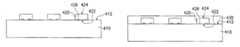
- FIG. 6is a schematic diagram showing the section view of the chip package structure of a preferred embodiment of the present invention with one die.
- FIG. 7is a schematic diagram showing the section view of the chip package structure of a preferred embodiment of the present invention with a plurality of dies.
- FIG. 8is a magnified diagram showing the sectional view of the chip package structure of a preferred embodiment of the present invention.
- FIG. 9A , 9 Bare schematic diagrams of the top and side view respectively of the patterned wiring layer of the thin-film circuit layer with a passive device.
- FIG. 10Ais a schematic diagram of the formation of a passive device by a single layer of patterned wiring layer of the thin-film circuit layer.
- FIG. 10Bis a schematic diagram of the formation of a passive device by a double layer of patterned wiring layer of the thin-film circuit layer.
- FIG. 11Ais a schematic diagram of the formation of a passive device by a single layer of patterned wiring layer of the thin-film circuit layer.
- FIG. 11Bis a schematic diagram of the formation of a passive device by a double layer of patterned wiring layer of the thin-film circuit layer.
- FIG. 11Cis a schematic diagram of the formation of a passive device by a double layer of patterned wiring layer of the thin-film circuit layer.
- a ceramic substrate 110 with a surface 112 usually of aluminum oxide material or other ceramic materialis provided.
- a plurality of dies 120 having an active surface 122 and a backside 124is also provided, where the active devices are formed on active surface 122 of the dies.
- dies 120have a plurality of metal pads 126 located on active surface 122 of dies 120 acting as the output terminal of dies 120 to transmit signals to the external circuitry.
- Backside 124 of dies 120is adhered to surface 112 of ceramic substrate 110 by a conductive paste or adhesive tape. Therefore, active surface 122 of dies 120 is facing upwards along surface 112 of ceramic substrate 110 .
- a filling layer 130can be formed on top of surface 112 of ceramic substrate 100 surrounding the peripheral of dies 120 to fill the gap between dies 120 .
- the height of filling layer 130should be approximately equal to the height of active surface 122 of dies 120 .
- the material of filling layer 130can be epoxy, polymer, or the like. After curing of filling layer 130 , a grinding or etching process is applied to planarize filling layer 130 so the top face of filling layer 130 is planar with active surface 122 of dies 120 .
- a dielectric layer 142is formed on top of filling layer 130 and active surface 122 of dies 120 .
- Dielectric layer 142is patterned according to metal pads 126 on dies 120 to form thru-holes 142 a .
- the material of dielectric layer 142can be poly-Imide (PI), benzocyclobutene (BCB), porous dielectric material, stress buffer material, or the like. Patternization of dielectric layer 142 can be performed by photo via, laser ablation, plasma etching, or the like.
- filling layer 130is used to support dielectric layer 142 so dielectric layer 142 can be formed planarized on top of ceramic substrate 110 and dies 120 without an uneven surface.
- dielectric layer 142also fills the peripheral of dies 120 , meaning the gap between dies 120 . Therefore the bottom structure of dielectric layer 142 can replace the structure of filling layer 130 covering entirely surface 112 of ceramic substrate 110 and surrounding dies 120 .
- the method of forming dielectric layer 142includes first depositing a layer of dielectric layer 142 entirely over dies 120 and ceramic substrate 110 , then after curing, a grinding or etching process is performed to planarize dielectric layer 142 .
- a patterned wiring layer 144is formed on top of dielectric layer 142 by photolithography and sputtering, electroplating, or electro-less plating. Wherein part of the conductive material from patterned wiring layer 144 will be injected into thru-holes 142 a to form vias 142 b , copper (Cu) is used as the material for patterned wiring layer 144 .
- thru-holes 142 acan be pre-filled with a conductive material such as a conductive glue to form vias 142 b .
- patterned wiring layer 144is electrically connected to metal pads 126 of dies 120 . It is to be noted that part of patterned wiring layer 144 extends to a region outside active surface 122 of dies 120 . Dielectric layer 142 and patterned wiring layer 144 form a thin-film circuit layer 140 .
- dielectric layer 146can be formed similarly to dielectric layer 142 on top of dielectric layer 142 and patterned wiring layer 144 .
- Dielectric layer 146is also patterned to form thru-holes 146 a , whereas thru-holes 146 a correspond to bonding pads 144 a of patterned wiring layer 144 .
- a patterned wiring layer 148can be formed on dielectric layer 146 in a similar way as patterned wiring layer 144 . Wherein part of the conductive material from patterned wiring layer 148 will be injected into thru-hole 146 a forming a via 146 b .
- patterned wiring layer 148is electrically connected to patterned wiring layer 144 by vias 146 b , and further electrically connected to metal pads 126 of die 120 by vias 142 b of thru-hole 142 a . Therefore, thin-film circuit layer 140 further comprises dielectric layer 146 , a plurality of vias 146 b , and patterned wiring layer 148 .
- the number of patterned wiring layers ( 144 , 148 . . . ) and dielectric layers ( 142 , 146 . . . ) for electrical insulationmay be increased. All patterned wiring layers ( 144 , 148 . . . ) are electrically connected by vias ( 146 b . . . ) of thru-holes ( 146 a . . . ). However if only the first patterned wiring layer 144 is required to entirely redistribute metal pads 126 of dies 120 on ceramic substrate 110 , extra dielectric layers ( 146 . . .
- thin-film circuit layer 140comprises at least one dielectric layer 142 , one patterned wiring layer 144 , and a plurality of vias 142 b .
- patterned wiring layer ( 144 , 148 . . . ) and vias ( 142 b , 146 b . . . ) of thin-film circuit layer 140form an external circuitry of thin-film circuit layer 140 .
- a patterned passivation layer 150is formed on top of dielectric layer 146 and patterned wiring layer 148 .
- Patterned passivation layer 150is used to protect patterned wiring layer 148 and expose the plurality of bonding pads 148 a of patterned wiring layer 148 , whereas some of bonding pads 148 a are in a region outside active surface 122 of dies 120 .
- the redistribution of metal pads 126 on ceramic substrate 110requires multiple layers of patterned wiring layers ( 144 , 148 . . . ) and a patterned passivation layer 150 formed on the very top, which is furthest away from ceramic substrate 110 .
- patterned passivation layer 150will be formed directly on patterned wiring layer 144 .
- the material of passivation layer 150can be anti-solder insulating coating or other insulating material.
- a bonding point 160can be placed on bonding pads 148 a serving as an interface for electrically connecting die 120 to the external circuitry.
- bonding point 160 illustrated in FIG. 1His a ball but it is not limited to any formation, which might include a bump, pin, or the like.
- Ball connectormaybe solder ball
- bump connectormaybe solder bump, gold bump, or the like.
- the first embodiment of the present inventionis a chip package structure with a ceramic substrate and a plurality of dies on it.
- the external circuitry of the thin-film circuit layerallows the metal pads of the die to fan out.
- bonding pads corresponding to the metal pads of the diessuch as solders balls, bumps, or pins as the signal input terminals, the distance of the signal path is effectively decreased. As a result, signal delay and attenuation are reduced to increase performance of the die.
- Ceramic materialpossesses advantageous properties such as high structural rigidity, high anti-corrosive properties, high density, and high thermal conductivity.
- Coefficient of thermal expansion (CTE) of aluminum oxide ceramic materialis comparable to that of iron-cobalt-nickel alloy.
- the present inventionspecifically applies the use of ceramic material due to its high structural rigidity, high anti-corrosive properties, high density, and high thermal conductivity, which means that the package structure can be used in unfavorable environments such as high-corrosiveness, high humidity, or high temperature environment.
- the high CTE of ceramic materialwill help the dies to dissipate heat for improved performance.
- the fabrication of ceramic-BGA (CBGA) substrateis already well know in the art, therefore current manufacturing machines can be easily adapted to manufacture the ceramic substrate of the present invention for lower cost.
- the second embodiment of the present inventiondiffers from the first embodiment by having inwardly protruded areas in the ceramic substrate. This area is for placement of the die with the backside of the die adhered to the bottom of the area so the overall thickness of the chip package structure is reduced.
- FIGS. 2A to 2Care schematic diagrams of the sectional view of the second embodiment illustrating the fabrication of the structure.
- a ceramic substrate 210 with a surface 212is provided.
- a plurality of inwardly protruded areas 214is formed on ceramic substrate 210 by machining such as milling.
- the depth of each inwardly protruded area 214is approximately equal to the thickness of die 220 , therefore the outline and depth of inwardly protruded areas 214 will be the same as dies 220 in FIG. 2C .
- backside 224 of dies 220is adhered to the bottom of inwardly protruded areas 214 so dies 220 are inlayed in inwardly protruded areas 214 .
- Active surface 222 of die 220is exposed along surface 212 or ceramic substrate 210 .
- An alternative method of forming inwardly protruded areas 214 in ceramic substrate 210 in FIG. 2Bis to use two green sheets 210 a and 210 b that are not sintered, as illustrated in FIG. 2D .
- Green sheet 210 ahas openings 214 a and by overlapping the two green sheets 210 a , 210 b and sintering them at a high temperature, opening 214 a in green sheet 210 a will form inwardly protruded areas 214 on green sheet 210 b as seen before in FIG. 2B , illustrated in FIG. 2E .
- the thickness of green sheet 210 ais approximately equal to that of die 220 so the depth of inwardly protruded areas 214 is approximately equal to the thickness of die 220 .
- the two green sheets 210 a and 210 b providedcan be already sintered before putting together. Openings 214 a can be formed before or after sintering green sheet 210 a . Following, the two green sheet 210 a , 210 b are overlapped to form inwardly protruded openings 214 in ceramic substrate 210 .
- the second embodiment of the present inventionis a ceramic substrate with a plurality of inwardly protruded areas for inlaying dies by adhering the backside of the dies to the bottom of the inwardly protruded areas and exposing the active surface of the dies.
- a thin-film circuit layeris formed on top of the dies and the ceramic substrate to fan out the metal pads of the dies by using the external circuitry of the thin-film circuit layer. Due to the inlay of the dies in the ceramic substrate, thinning of the thickness of the chip package structure is effectively achieved and the surface of the ceramic substrate provides enough planarity and support for the formation of the thin-film circuit layer.
- the third embodiment of the present inventiondiffers from the second embodiment of the present invention by using an integrated ceramic substrate with at least one ceramic layer and one heat conducting layer.
- FIGS. 3A to 3Care schematic diagrams of the sectional view of the third embodiment illustrating the fabrication of the structure.
- an integrated ceramic substrate 310consists of a ceramic layer 310 a with multiple openings 314 a and a heat conducting layer 310 b , wherein the material of heat conducting layer 310 b maybe metal.
- ceramic layer 310 ais placed overlapping heat conducting layer 310 b so openings 314 a of ceramic layer 310 a form inwardly protruded areas 314 .
- backside 324 of die 320is adhered to the bottom of inwardly protruded areas 314 so dies 320 are inlayed in ceramic substrate 310 with active surface 322 of die 320 exposed along surface 312 of ceramic board 310 .
- FIG. 3Aa non-sintered ceramic layer (green sheet) 310 a with openings 314 a is provided, and in FIG. 3B , the non-sintered ceramic layer 310 a is overlapped on heat conductive layer 310 b so openings 314 a of ceramic layer 310 a can form inwardly protruded areas 314 on the surface of heat conducting layer 310 b .
- integrated ceramic substrate 310 with ceramic layer 310 a and heat conducting layer 310 bare sintered at a temperature above 1000° C. Therefore the material of heat conducting layer 310 b must have a higher melting temperature than the temperature used for sintering the green sheet.
- the alternative methodis using an already-sintered ceramic layer 310 a with openings 314 a .
- the already-sintered ceramic substrate layer 310 ais overlapped on heat conducting layer 310 b so openings 314 a of ceramic layer 310 a can form inwardly protruded areas 314 .
- the thickness of ceramic layer 310 ais approximately equal to that of die 320 so the depth of openings 314 a is also approximately equal to the thickness of die 320 .
- the third embodiment of the present inventionis an integrated ceramic substrate with a ceramic layer with a plurality of openings and a heat conducting layer.
- the openings in the ceramic layerwill form inwardly protruded areas on the integrated ceramic substrate.
- Backside of the dieadheres to the bottom of the inwardly protruded areas so the dies are inlayed in the inwardly protruded areas exposing the active surface of the dies.
- This integrated ceramic substratecan efficiently dissipate heat from the dies to the outside because the bottom of the inwardly protruded area is the surface of the heat conducting material.
- the surface of the ceramic substrateprovides enough planarity and support for the formation of the thin-film circuit layer.
- FIGS. 4A to 4Eare schematic diagrams of the sectional view of the fourth embodiment illustrating the fabrication of the structure.
- a ceramic substrate 410 with a first surface 412 and a plurality of dies 420are provided.
- the dies 420have an active surface 422 , a backside 424 , and a plurality of metal pads 426 located on active surface 422 .
- the fourth embodiment of the present inventiondiffers from the third embodiment of the present invention by placing active surface 422 of die 420 downwards facing first surface 412 of ceramic substrate 410 .
- a filling layer 430is formed on top of first surface 412 of ceramic substrate 410 after active surface 422 of die 420 is adhered to first surface 412 of ceramic substrate 410 .
- Filling layer 430covers entirely first surface 412 of ceramic substrate 410 and surrounds dies 420 .
- the material of filling layer 430maybe an oxide, epoxy, or the like.
- a planarization processsuch as grinding is performed to planarize filling layer 430 and backside 424 of dies 420 .
- the thickness of the active devices and wiring (not shown) on active surface 422 of die 420is much less than that of dies 420 , the thickness of die 420 should not be too small because cracks or damage to the die will occur during machine handling.
- the present inventiondirectly adheres active surface 422 of dies 420 to first surface 412 of ceramic substrate 410 without further machine handling.
- a grinding processis performed on backside 424 of dies 420 to reduce the thickness of dies 420 .
- dies 420are ground to a very small thickness allowing the final chip package structure to be much thinner.
- a second ceramic substrate 440 with a second surface 442is adhered to filling layer 430 and dies 420 creating a sandwich effect with filling layer 430 and dies 420 in between two ceramic substrates 410 and 440 .
- First ceramic substrate 410is used to provide a planar surface for dies 420 to adhere to and to serve as an insulating layer. Therefore ceramic substrate 410 can be replaced by substrate made of glass or other organic material.
- first thru-holes 410 aare formed on first ceramic substrate 410 for exposing metal pads 426 of active surface 422 of die 420 .
- First thru-holes 410 acan be formed by machine drilling, laser, plasma etching, or similar methods.
- a first patterned wiring layer 450is formed on first ceramic substrate 410 .
- first vias 410 b in first thru-holes 410 aare formed by either filling first thru-holes 410 a with part of the conductive material from patterned wiring layer 450 or pre-filling first thru-holes 410 a with a conductive material before the formation of patterned wiring layer 450 .
- a part of patterned wiring layer 450will extend to a region outside active surface 422 of die 420 .
- a dielectric layer 462is formed on first ceramic substrate 410 and first patterned wiring layer 450 .
- dielectric layer 462is patterned to form a plurality of second thru-holes 462 a , which correspond to bonding pad 450 a of patterned wiring layer 450 .
- a second patterned wiring layer 464is formed on dielectric layer 462 .
- second vias 462 b in second thru-holes 462 acan be formed by either filling second thru-holes 462 a with part of the conductive material from patterned wiring layer or pre-fill second thru-holes 462 a with a conductive material before the formation of patterned wiring layer 464 .
- first ceramic substrate 410 , first patterned wiring layer 450 , dielectric layer 462 . . . , and second patterned wiring layer 464 . . .form thin-film circuit layer 460 .
- First vias 410 b , first patterned wiring layer 450 , second vias 462 b . . . , and second patterned wiring layer 464form the external circuitry of thin-film circuit layer 460 .
- the fourth embodiment of the present inventionis a ceramic substrate with the active surface of the dies directly adhered to the surface of the first ceramic substrate.
- a filling layeris formed over the dies and the ceramic substrate followed by a planarization and thinning process.
- a second ceramic substrateis adhered to the die and the filling layer.
- a thinning process of the first ceramic substrateis performed and a plurality of thru-holes filled with conductive material are formed on the first ceramic substrate.
- a patterned wiring layeris formed on the first ceramic substrate allowing the external circuitry of the thin-film circuit layer to extend to a region outside the active surface of the die to help fan out the metal pads of the die.
- the advantage of this structureis increased surface stability and accuracy because the active surface of the dies are first adhered to the surface of the first ceramic substrate.
- the thickness of the diecan be very small for reducing the overall thickness of the chip package because no machine handling of dies is required.
- the fifth embodiment of the present inventiontakes the first half of the fabrication process from the fourth embodiment of the present invention and combines with the second half of the fabrication process from the first embodiment of the present invention.
- FIGS. 5A to 5Eare schematic diagrams of the sectional view illustrating the fabrication of the structure.
- an active surface 522 of dies 520is adhered to a first surface 512 of a first ceramic substrate 510 .
- a filling layer 530is formed on top of dies 520 and first ceramic substrate 510 covering dies 520 .
- a planarization and thinning process of dies 520 and filling layer 530is performed to planarize backside 524 of dies 520 and filling layer 530 .
- a second ceramic substrate 540is formed on top of dies 520 and filling layer 530 so backside 524 of dies 520 adheres to second ceramic substrate 540 .
- First ceramic substrate 510is used to supply a planarized surface (first surface 512 ), and will be removed in later stages of the fabrication process. Therefore first ceramic substrate 510 can be replaced by substrates of other materials such as glass, metal, silicon, or other organic material.
- the fifth embodiment of the present inventionis a ceramic substrate with the active surface of the die adhered to the surface of the first ceramic substrate for allowing high surface stability and accuracy. As a result, it eliminates the need of machine handling of the dies to achieve a very small thickness of the die for reducing the overall thickness of the chip package.
- FIG. 6it illustrates the schematic diagram of the sectional view of the chip package structure 600 of the present invention for a single die 620 .
- Die 620is placed on ceramic substrate 610 , and a thin-film circuit layer 640 is formed on top of dies 620 and ceramic substrate 610 .
- External circuitry 642 of thin-film circuit layer 640has at least has one patterned wiring layer 642 a and a plurality of vias 642 b .
- the thickness of the inner traces inside die 620is usually under 1 micron, but because the high amount of traces collocated together so RC delay is relatively high and the power/ground bus requires a large area. As a result, the area of die 620 is not enough to accommodate the power/ground bus.
- the chip package structure 600uses thin-film circuit layer 640 and external circuitry 642 with wider, thicker, and longer traces to alleviate the problem. These traces act an interface for transmitting signals for the internal circuitry of die 620 or the power/ground bus of die 620 . This will improve the performance of die 620 .
- FIG. 8it illustrates a magnified view of the sectional view of the chip package structure of the present invention.
- Active surface 622 of die 620has a plurality of active devices 628 a , 628 b , and an internal circuitry 624 .
- the internal circuitry 624forms a plurality of metal pads 626 on the surface of die 620 . Therefore signals are transmitted from active devices 628 a to external circuitry 642 via internal circuitry 624 of die 620 , and from external circuitry 642 back to another active device 628 b via internal circuitry 624 .
- the traces of external circuitry 642are wider, longer, and thicker than that of internal circuitry 624 for providing an improved transmission path.
- external circuitry 642further comprises at least one passive device 644 including a capacitor, an inductor, a resistor, a wave-guide, a filter, a micro electronic mechanical sensor (MEMS), or the like.
- Passive device 644can be located on a single layer of patterned wiring layer 642 a or between two layers of patterned wiring layers 642 a .
- passive device 644can be formed by printing or other method on two bonding points on patterned wiring layer 642 a when forming thin-film layer 640 .
- a comb-shape passive device 644(such as a comb capacitor) is formed directly on a single patterned wiring layer.
- FIG. 10Aa comb-shape passive device 644 (such as a comb capacitor) is formed directly on a single patterned wiring layer.
- passive device 644(such as a capacitor) is formed between two layers of patterned wiring layers 642 a with an insulating material 646 in between. Wherein the original dielectric layer (not shown) can replace insulating material 646 .
- passive device 644(such as an inductor) is formed by making a single layer of patterned wiring layer 642 a into a circular or square (not shown) spiral.
- column-shape passive device 644(such as an inductor) is formed by using two layers of patterned wiring layers 642 a and a plurality of vias 642 b to surround an insulating material 646 forming a column.
- FIG. 11Apassive device 644 (such as an inductor) is formed by making a single layer of patterned wiring layer 642 a into a circular or square (not shown) spiral.
- column-shape passive device 644(such as an inductor) is formed by using two layers of patterned wiring layers 642 a and a plurality of vias 642 b
- circular-shaped passive device 644(such as an inductor) is formed by using slanted traces from two layers of patterned wiring layers and a plurality of vias 642 b to surround an insulating material 646 in a circular manner forming a pie.
- the above structuresallow the original externally welded passive devices to be integrated into the inside of the chip package structure.
- FIG. 6illustrates a chip package structure 600 for a single die 620 but FIG. 7 illustrates a chip package structure 700 for a plurality of dies.
- Chip package structure 700 in FIG. 7differs from chip package structure 600 in FIG. 6 by having a die module 720 , which comprises at least one or more dies such as die 720 a , 720 b .
- Die 720 a , 720 bare electrically connected by the external circuitry of the thin-film circuit layer.
- the function of die 720 a , 720 bcan be the same or different and can be integrated together by external circuitry 742 to form a multi-die module (MCM) by packaging same or different dies into one chip package structure.
- MCMmulti-die module
- the present inventionprovides a chip packaging method by adhering a die to a ceramic substrate or to an inwardly protruded area of a ceramic substrate, and forming a thin-film circuit layer with bonding pads and points above the die and ceramic substrate.
- This structurecan fan out the metal pads on the die to achieve a thin chip package structure with high pin count.
- the chip package of the present inventionis performed directly on the die and the ceramic substrate for fanning out the metal pads on the die. It does not require flip chip or wire bonding to connect the die to the micro-spaced contact points of a package substrate or carrier.
- the present inventioncan reduce cost because the package substrate with micro-spaced contacts is very expensive.
- the signal transmission path of the present inventionis reduced to lessen the effect of signal delay and attenuation, which improves the performance of the die.
- the present inventionuses ceramic substrate with high structural rigidity, high anti-corrosive properties, high density, and high thermal conductivity, which means that the package structure can be used in unfavorable environments such as high-corrosive, high humidity, or high temperature environment.
- the high CTE of ceramic materialwill help the die dissipate heat to improve performance.
- ceramic-BGACBGA is already well know in the skilled of the art, which can be adapted to current machines to manufacture the ceramic substrate of the present invention for lower cost.
- the third embodiment of the present inventionprovides an integrated substrate comprises a ceramic layer and a heat conducting layer.
- a plurality of openingscan be pre-formed on the ceramic layer so inwardly protruded areas are formed for inlaying the die when the ceramic layer overlaps the heat conducting layer.
- the heat conducting layerhelps to dissipate heat to the outside from the die during operation, which will effectively increase performance.
- the thin-film layer circuit of the present inventionis used to transmit signals between two main active devices inside the die, or used as a power/ground bus, or used to add in passive devices. Furthermore, the chip package structure of the present invention can accommodate one or more dies with similar or different functions.
- the external circuitry of the thin-film circuit layerelectrically connects the multiple dies together and can be used in a MCM package.
- the chip package structure of the present inventionadapts the MCM, the external circuitry of the thin-film circuit layer, the passive devices of the external circuitry to form a package that is “system in package”.
Landscapes
- Engineering & Computer Science (AREA)
- Computer Hardware Design (AREA)
- Microelectronics & Electronic Packaging (AREA)
- Power Engineering (AREA)
- Physics & Mathematics (AREA)
- Condensed Matter Physics & Semiconductors (AREA)
- General Physics & Mathematics (AREA)
- Manufacturing & Machinery (AREA)
- Production Of Multi-Layered Print Wiring Board (AREA)
- Internal Circuitry In Semiconductor Integrated Circuit Devices (AREA)
- Semiconductor Integrated Circuits (AREA)
- Structure Of Printed Boards (AREA)
Abstract
Description
Claims (43)
Priority Applications (2)
| Application Number | Priority Date | Filing Date | Title |
|---|---|---|---|
| US10/454,972US8535976B2 (en) | 2001-12-31 | 2003-06-04 | Method for fabricating chip package with die and substrate |
| US13/887,093US8835221B2 (en) | 2001-12-31 | 2013-05-03 | Integrated chip package structure using ceramic substrate and method of manufacturing the same |
Applications Claiming Priority (5)
| Application Number | Priority Date | Filing Date | Title |
|---|---|---|---|
| TW090133092ATW584950B (en) | 2001-12-31 | 2001-12-31 | Chip packaging structure and process thereof |
| TW90133092A | 2001-12-31 | ||
| TW90133092 | 2001-12-31 | ||
| US10/055,498US6800941B2 (en) | 2001-12-31 | 2002-01-22 | Integrated chip package structure using ceramic substrate and method of manufacturing the same |
| US10/454,972US8535976B2 (en) | 2001-12-31 | 2003-06-04 | Method for fabricating chip package with die and substrate |
Related Parent Applications (1)
| Application Number | Title | Priority Date | Filing Date |
|---|---|---|---|
| US10/055,498DivisionUS6800941B2 (en) | 2001-12-31 | 2002-01-22 | Integrated chip package structure using ceramic substrate and method of manufacturing the same |
Related Child Applications (1)
| Application Number | Title | Priority Date | Filing Date |
|---|---|---|---|
| US13/887,093DivisionUS8835221B2 (en) | 2001-12-31 | 2013-05-03 | Integrated chip package structure using ceramic substrate and method of manufacturing the same |
Publications (2)
| Publication Number | Publication Date |
|---|---|
| US20030205804A1 US20030205804A1 (en) | 2003-11-06 |
| US8535976B2true US8535976B2 (en) | 2013-09-17 |
Family
ID=21680113
Family Applications (3)
| Application Number | Title | Priority Date | Filing Date |
|---|---|---|---|
| US10/055,498Expired - Fee RelatedUS6800941B2 (en) | 2001-12-31 | 2002-01-22 | Integrated chip package structure using ceramic substrate and method of manufacturing the same |
| US10/454,972Expired - Fee RelatedUS8535976B2 (en) | 2001-12-31 | 2003-06-04 | Method for fabricating chip package with die and substrate |
| US13/887,093Expired - Fee RelatedUS8835221B2 (en) | 2001-12-31 | 2013-05-03 | Integrated chip package structure using ceramic substrate and method of manufacturing the same |
Family Applications Before (1)
| Application Number | Title | Priority Date | Filing Date |
|---|---|---|---|
| US10/055,498Expired - Fee RelatedUS6800941B2 (en) | 2001-12-31 | 2002-01-22 | Integrated chip package structure using ceramic substrate and method of manufacturing the same |
Family Applications After (1)
| Application Number | Title | Priority Date | Filing Date |
|---|---|---|---|
| US13/887,093Expired - Fee RelatedUS8835221B2 (en) | 2001-12-31 | 2013-05-03 | Integrated chip package structure using ceramic substrate and method of manufacturing the same |
Country Status (2)
| Country | Link |
|---|---|
| US (3) | US6800941B2 (en) |
| TW (1) | TW584950B (en) |
Cited By (5)
| Publication number | Priority date | Publication date | Assignee | Title |
|---|---|---|---|---|
| US8835221B2 (en) | 2001-12-31 | 2014-09-16 | Qualcomm Incorporated | Integrated chip package structure using ceramic substrate and method of manufacturing the same |
| US20170278836A1 (en)* | 2012-08-02 | 2017-09-28 | Infineon Technologies Ag | Integrated System and Method of Making the Integrated System |
| US10313157B2 (en)* | 2017-04-25 | 2019-06-04 | Realtek Semiconductor Corp. | Apparatus and method for multiplexing multi-lane multi-mode data transport |
| US10622346B2 (en)* | 2016-10-04 | 2020-04-14 | Infineon Technologies Ag | Method for manufacturing an electronic device and electronic device |
| US11119962B2 (en) | 2017-04-25 | 2021-09-14 | Realtek Semiconductor Corp. | Apparatus and method for multiplexing data transport by switching different data protocols through a common bond pad |
Families Citing this family (93)
| Publication number | Priority date | Publication date | Assignee | Title |
|---|---|---|---|---|
| US7271489B2 (en) | 2003-10-15 | 2007-09-18 | Megica Corporation | Post passivation interconnection schemes on top of the IC chips |
| US6673698B1 (en)* | 2002-01-19 | 2004-01-06 | Megic Corporation | Thin film semiconductor package utilizing a glass substrate with composite polymer/metal interconnect layers |
| TW503496B (en) | 2001-12-31 | 2002-09-21 | Megic Corp | Chip packaging structure and manufacturing process of the same |
| TW544882B (en) | 2001-12-31 | 2003-08-01 | Megic Corp | Chip package structure and process thereof |
| TW517361B (en) | 2001-12-31 | 2003-01-11 | Megic Corp | Chip package structure and its manufacture process |
| US7096581B2 (en)* | 2002-03-06 | 2006-08-29 | Stmicroelectronics, Inc. | Method for providing a redistribution metal layer in an integrated circuit |
| US7037805B2 (en)* | 2003-05-07 | 2006-05-02 | Honeywell International Inc. | Methods and apparatus for attaching a die to a substrate |
| US6927098B2 (en)* | 2003-05-07 | 2005-08-09 | Honeywell International Inc. | Methods and apparatus for attaching MEMS devices to housing |
| DE10334577B3 (en)* | 2003-07-28 | 2005-02-10 | Infineon Technologies Ag | A method of applying a rewiring to a benefit by compensating for positional errors and semiconductor chips in component positions of the benefit |
| US6982482B2 (en)* | 2004-02-24 | 2006-01-03 | Applied Pulsed Power, Inc. | Packaging of solid state devices |
| TWI331370B (en) | 2004-06-18 | 2010-10-01 | Megica Corp | Connection between two circuitry components |
| JP3961537B2 (en)* | 2004-07-07 | 2007-08-22 | 日本電気株式会社 | Manufacturing method of semiconductor mounting wiring board and manufacturing method of semiconductor package |
| US8067837B2 (en) | 2004-09-20 | 2011-11-29 | Megica Corporation | Metallization structure over passivation layer for IC chip |
| DE102004063994B4 (en)* | 2004-10-26 | 2009-01-02 | Advanced Chip Engineering Technology Inc. | Chip-sized packing structure |
| DE102004058413B4 (en)* | 2004-10-26 | 2006-10-19 | Advanced Chip Engineering Technology Inc. | Method for producing a chip-size packing structure |
| KR101313391B1 (en) | 2004-11-03 | 2013-10-01 | 테세라, 인코포레이티드 | Stacked packaging improvements |
| TWI335069B (en) | 2005-07-15 | 2010-12-21 | Ryo Takatsuki | Ic chip component, multi chip module, integrated structure thereof and method for manufacturing them |
| CN100505252C (en)* | 2005-10-27 | 2009-06-24 | 全懋精密科技股份有限公司 | Embedded chip package structure |
| US7491567B2 (en)* | 2005-11-22 | 2009-02-17 | Honeywell International Inc. | MEMS device packaging methods |
| US20070114643A1 (en)* | 2005-11-22 | 2007-05-24 | Honeywell International Inc. | Mems flip-chip packaging |
| US8058101B2 (en) | 2005-12-23 | 2011-11-15 | Tessera, Inc. | Microelectronic packages and methods therefor |
| TWI308382B (en)* | 2006-07-25 | 2009-04-01 | Phoenix Prec Technology Corp | Package structure having a chip embedded therein and method fabricating the same |
| US7569422B2 (en)* | 2006-08-11 | 2009-08-04 | Megica Corporation | Chip package and method for fabricating the same |
| US7598610B2 (en)* | 2007-01-04 | 2009-10-06 | Phoenix Precision Technology Corporation | Plate structure having chip embedded therein and the manufacturing method of the same |
| US7964961B2 (en)* | 2007-04-12 | 2011-06-21 | Megica Corporation | Chip package |
| US7612457B2 (en)* | 2007-06-21 | 2009-11-03 | Infineon Technologies Ag | Semiconductor device including a stress buffer |
| US8212155B1 (en)* | 2007-06-26 | 2012-07-03 | Wright Peter V | Integrated passive device |
| US7701037B2 (en)* | 2007-07-31 | 2010-04-20 | International Business Machines Corporation | Orientation-independent multi-layer BEOL capacitor |
| US20100025848A1 (en)* | 2008-08-04 | 2010-02-04 | Infineon Technologies Ag | Method of fabricating a semiconductor device and semiconductor device |
| US8201326B2 (en)* | 2008-12-23 | 2012-06-19 | Infineon Technologies Ag | Method of manufacturing a semiconductor device |
| US20100167471A1 (en) | 2008-12-30 | 2010-07-01 | Stmicroelectronics Asia Pacific Pte. Ltd. | Reducing warpage for fan-out wafer level packaging |
| US8003515B2 (en) | 2009-09-18 | 2011-08-23 | Infineon Technologies Ag | Device and manufacturing method |
| US20110156239A1 (en)* | 2009-12-29 | 2011-06-30 | Stmicroelectronics Asia Pacific Pte Ltd. | Method for manufacturing a fan-out embedded panel level package |
| US8482111B2 (en) | 2010-07-19 | 2013-07-09 | Tessera, Inc. | Stackable molded microelectronic packages |
| US9159708B2 (en) | 2010-07-19 | 2015-10-13 | Tessera, Inc. | Stackable molded microelectronic packages with area array unit connectors |
| KR101075241B1 (en) | 2010-11-15 | 2011-11-01 | 테세라, 인코포레이티드 | Microelectronic package with terminals in dielectric member |
| US20120146206A1 (en) | 2010-12-13 | 2012-06-14 | Tessera Research Llc | Pin attachment |
| CN102593085B (en)* | 2011-01-10 | 2014-08-13 | 原相科技股份有限公司 | Chip packaging structure and chip packaging process |
| US8618659B2 (en) | 2011-05-03 | 2013-12-31 | Tessera, Inc. | Package-on-package assembly with wire bonds to encapsulation surface |
| KR101128063B1 (en) | 2011-05-03 | 2012-04-23 | 테세라, 인코포레이티드 | Package-on-package assembly with wire bonds to encapsulation surface |
| US8872318B2 (en) | 2011-08-24 | 2014-10-28 | Tessera, Inc. | Through interposer wire bond using low CTE interposer with coarse slot apertures |
| US8836136B2 (en) | 2011-10-17 | 2014-09-16 | Invensas Corporation | Package-on-package assembly with wire bond vias |
| US8772058B2 (en)* | 2012-02-02 | 2014-07-08 | Harris Corporation | Method for making a redistributed wafer using transferrable redistribution layers |
| US8946757B2 (en) | 2012-02-17 | 2015-02-03 | Invensas Corporation | Heat spreading substrate with embedded interconnects |
| US8372741B1 (en) | 2012-02-24 | 2013-02-12 | Invensas Corporation | Method for package-on-package assembly with wire bonds to encapsulation surface |
| US9349706B2 (en) | 2012-02-24 | 2016-05-24 | Invensas Corporation | Method for package-on-package assembly with wire bonds to encapsulation surface |
| US8835228B2 (en) | 2012-05-22 | 2014-09-16 | Invensas Corporation | Substrate-less stackable package with wire-bond interconnect |
| KR101947722B1 (en)* | 2012-06-07 | 2019-04-25 | 삼성전자주식회사 | stack semiconductor package and method of manufacturing the same |
| US9391008B2 (en) | 2012-07-31 | 2016-07-12 | Invensas Corporation | Reconstituted wafer-level package DRAM |
| US9502390B2 (en) | 2012-08-03 | 2016-11-22 | Invensas Corporation | BVA interposer |
| JP6282425B2 (en)* | 2012-10-29 | 2018-02-21 | 新光電気工業株式会社 | Wiring board manufacturing method |
| US8975738B2 (en) | 2012-11-12 | 2015-03-10 | Invensas Corporation | Structure for microelectronic packaging with terminals on dielectric mass |
| US9431369B2 (en) | 2012-12-13 | 2016-08-30 | Taiwan Semiconductor Manufacturing Company, Ltd. | Antenna apparatus and method |
| US8878353B2 (en) | 2012-12-20 | 2014-11-04 | Invensas Corporation | Structure for microelectronic packaging with bond elements to encapsulation surface |
| US9136254B2 (en) | 2013-02-01 | 2015-09-15 | Invensas Corporation | Microelectronic package having wire bond vias and stiffening layer |
| US8883563B1 (en) | 2013-07-15 | 2014-11-11 | Invensas Corporation | Fabrication of microelectronic assemblies having stack terminals coupled by connectors extending through encapsulation |
| US9023691B2 (en) | 2013-07-15 | 2015-05-05 | Invensas Corporation | Microelectronic assemblies with stack terminals coupled by connectors extending through encapsulation |
| US9034696B2 (en) | 2013-07-15 | 2015-05-19 | Invensas Corporation | Microelectronic assemblies having reinforcing collars on connectors extending through encapsulation |
| US9167710B2 (en) | 2013-08-07 | 2015-10-20 | Invensas Corporation | Embedded packaging with preformed vias |
| US9685365B2 (en) | 2013-08-08 | 2017-06-20 | Invensas Corporation | Method of forming a wire bond having a free end |
| US20150076714A1 (en) | 2013-09-16 | 2015-03-19 | Invensas Corporation | Microelectronic element with bond elements to encapsulation surface |
| US9082753B2 (en) | 2013-11-12 | 2015-07-14 | Invensas Corporation | Severing bond wire by kinking and twisting |
| US9087815B2 (en) | 2013-11-12 | 2015-07-21 | Invensas Corporation | Off substrate kinking of bond wire |
| US9583456B2 (en) | 2013-11-22 | 2017-02-28 | Invensas Corporation | Multiple bond via arrays of different wire heights on a same substrate |
| US9379074B2 (en) | 2013-11-22 | 2016-06-28 | Invensas Corporation | Die stacks with one or more bond via arrays of wire bond wires and with one or more arrays of bump interconnects |
| US9263394B2 (en) | 2013-11-22 | 2016-02-16 | Invensas Corporation | Multiple bond via arrays of different wire heights on a same substrate |
| US9824989B2 (en) | 2014-01-17 | 2017-11-21 | Taiwan Semiconductor Manufacturing Company, Ltd. | Fan-out package and methods of forming thereof |
| US9583411B2 (en) | 2014-01-17 | 2017-02-28 | Invensas Corporation | Fine pitch BVA using reconstituted wafer with area array accessible for testing |
| US9214454B2 (en) | 2014-03-31 | 2015-12-15 | Invensas Corporation | Batch process fabrication of package-on-package microelectronic assemblies |
| US10381326B2 (en) | 2014-05-28 | 2019-08-13 | Invensas Corporation | Structure and method for integrated circuits packaging with increased density |
| US9646917B2 (en) | 2014-05-29 | 2017-05-09 | Invensas Corporation | Low CTE component with wire bond interconnects |
| US9412714B2 (en) | 2014-05-30 | 2016-08-09 | Invensas Corporation | Wire bond support structure and microelectronic package including wire bonds therefrom |
| TWI655727B (en) | 2014-06-17 | 2019-04-01 | 恆勁科技股份有限公司 | Package substrate and flip-chip package circuit including the same |
| CN104064524B (en)* | 2014-06-27 | 2017-03-29 | 通富微电子股份有限公司 | The forming method of radio-frequency module |
| CN105448883B (en)* | 2014-08-12 | 2017-11-24 | 碁鼎科技秦皇岛有限公司 | Chip package base plate and, chip-packaging structure and the preparation method of the two |
| US9735084B2 (en) | 2014-12-11 | 2017-08-15 | Invensas Corporation | Bond via array for thermal conductivity |
| US9888579B2 (en) | 2015-03-05 | 2018-02-06 | Invensas Corporation | Pressing of wire bond wire tips to provide bent-over tips |
| US9502372B1 (en) | 2015-04-30 | 2016-11-22 | Invensas Corporation | Wafer-level packaging using wire bond wires in place of a redistribution layer |
| US9761554B2 (en) | 2015-05-07 | 2017-09-12 | Invensas Corporation | Ball bonding metal wire bond wires to metal pads |
| KR101664411B1 (en)* | 2015-06-04 | 2016-10-14 | 주식회사 에스에프에이반도체 | Method for manufacturing wafer leven fan out package |
| US9490222B1 (en) | 2015-10-12 | 2016-11-08 | Invensas Corporation | Wire bond wires for interference shielding |
| US10490528B2 (en) | 2015-10-12 | 2019-11-26 | Invensas Corporation | Embedded wire bond wires |
| US10332854B2 (en) | 2015-10-23 | 2019-06-25 | Invensas Corporation | Anchoring structure of fine pitch bva |
| US10181457B2 (en) | 2015-10-26 | 2019-01-15 | Invensas Corporation | Microelectronic package for wafer-level chip scale packaging with fan-out |
| US9786592B2 (en)* | 2015-10-30 | 2017-10-10 | Taiwan Semiconductor Manufacturing Co., Ltd. | Integrated circuit structure and method of forming the same |
| US10043779B2 (en) | 2015-11-17 | 2018-08-07 | Invensas Corporation | Packaged microelectronic device for a package-on-package device |
| US9659848B1 (en) | 2015-11-18 | 2017-05-23 | Invensas Corporation | Stiffened wires for offset BVA |
| US9984992B2 (en) | 2015-12-30 | 2018-05-29 | Invensas Corporation | Embedded wire bond wires for vertical integration with separate surface mount and wire bond mounting surfaces |
| US9704796B1 (en)* | 2016-02-11 | 2017-07-11 | Qualcomm Incorporated | Integrated device comprising a capacitor that includes multiple pins and at least one pin that traverses a plate of the capacitor |
| US9935075B2 (en) | 2016-07-29 | 2018-04-03 | Invensas Corporation | Wire bonding method and apparatus for electromagnetic interference shielding |
| US10299368B2 (en) | 2016-12-21 | 2019-05-21 | Invensas Corporation | Surface integrated waveguides and circuit structures therefor |
| US10032707B2 (en) | 2016-12-27 | 2018-07-24 | Intel Corporation | Post-grind die backside power delivery |
| CN116131092A (en)* | 2021-11-15 | 2023-05-16 | 赫芯(浙江)微电子科技有限公司 | Semiconductor laser packaging structure, laser and manufacturing method |
Citations (377)
| Publication number | Priority date | Publication date | Assignee | Title |
|---|---|---|---|---|
| US2920232A (en) | 1958-08-18 | 1960-01-05 | Gen Electric | Display device with storage |
| US3504214A (en) | 1967-01-13 | 1970-03-31 | Westinghouse Canada Ltd | Electroluminescent display device |
| US3634714A (en) | 1970-02-16 | 1972-01-11 | G T Schijeldahl Co | Electroluminescent display device with apertured electrodes |
| US3677112A (en) | 1970-06-08 | 1972-07-18 | John W Keniston | Pincers |
| US3903590A (en) | 1973-03-10 | 1975-09-09 | Tokyo Shibaura Electric Co | Multiple chip integrated circuits and method of manufacturing the same |
| US4021838A (en) | 1974-11-20 | 1977-05-03 | International Business Machines Corporation | Semiconductor integrated circuit devices |
| US4235498A (en) | 1979-07-26 | 1980-11-25 | The Bendix Corporation | Electrical connector with locking means |
| US4402888A (en) | 1981-09-14 | 1983-09-06 | Pamarco Incorporated | Corona discharge treatment roll |
| US4622058A (en)* | 1984-06-22 | 1986-11-11 | International Business Machines Corporation | Formation of a multi-layer glass-metallized structure formed on and interconnected to multi-layered-metallized ceramic substrate |
| US4685998A (en) | 1984-03-22 | 1987-08-11 | Thomson Components - Mostek Corp. | Process of forming integrated circuits with contact pads in a standard array |
| US4789647A (en) | 1986-01-08 | 1988-12-06 | U.S. Philips Corporation | Method of manufacturing a semiconductor device, in which a metallization with a thick connection electrode is provided on a semiconductor body |
| US4840923A (en) | 1986-04-30 | 1989-06-20 | International Business Machine Corporation | Simultaneous multiple level interconnection process |
| US4866501A (en) | 1985-12-16 | 1989-09-12 | American Telephone And Telegraph Company At&T Bell Laboratories | Wafer scale integration |
| US4918811A (en) | 1986-09-26 | 1990-04-24 | General Electric Company | Multichip integrated circuit packaging method |
| US5048179A (en) | 1986-05-23 | 1991-09-17 | Ricoh Company, Ltd. | IC chip mounting method |
| US5049980A (en) | 1987-04-15 | 1991-09-17 | Kabushiki Kaisha Toshiba | Electronic circuit device and method of manufacturing same |
| US5055321A (en) | 1988-04-28 | 1991-10-08 | Ibiden Co., Ltd. | Adhesive for electroless plating, printed circuit boards and method of producing the same |
| US5063177A (en) | 1990-10-04 | 1991-11-05 | Comsat | Method of packaging microwave semiconductor components and integrated circuits |
| US5073814A (en) | 1990-07-02 | 1991-12-17 | General Electric Company | Multi-sublayer dielectric layers |
| US5081563A (en) | 1990-04-27 | 1992-01-14 | International Business Machines Corporation | Multi-layer package incorporating a recessed cavity for a semiconductor chip |
| US5083187A (en) | 1990-05-16 | 1992-01-21 | Texas Instruments Incorporated | Integrated circuit device having bumped power supply buses over active surface areas and method of manufacture thereof |
| US5095402A (en) | 1990-10-02 | 1992-03-10 | Rogers Corporation | Internally decoupled integrated circuit package |
| US5099306A (en) | 1988-11-21 | 1992-03-24 | Honeywell Inc. | Stacked tab leadframe assembly |
| US5111278A (en) | 1991-03-27 | 1992-05-05 | Eichelberger Charles W | Three-dimensional multichip module systems |
| US5149662A (en) | 1991-03-27 | 1992-09-22 | Integrated System Assemblies Corporation | Methods for testing and burn-in of integrated circuit chips |
| US5161093A (en) | 1990-07-02 | 1992-11-03 | General Electric Company | Multiple lamination high density interconnect process and structure employing a variable crosslinking adhesive |
| US5188984A (en)* | 1987-04-21 | 1993-02-23 | Sumitomo Electric Industries, Ltd. | Semiconductor device and production method thereof |
| US5196377A (en) | 1990-12-20 | 1993-03-23 | Cray Research, Inc. | Method of fabricating silicon-based carriers |
| US5211278A (en) | 1990-01-31 | 1993-05-18 | Lamb-Weston, Inc. | Food transport chain conveyor system |
| US5226232A (en) | 1990-05-18 | 1993-07-13 | Hewlett-Packard Company | Method for forming a conductive pattern on an integrated circuit |
| US5239198A (en) | 1989-09-06 | 1993-08-24 | Motorola, Inc. | Overmolded semiconductor device having solder ball and edge lead connective structure |
| US5241456A (en)* | 1990-07-02 | 1993-08-31 | General Electric Company | Compact high density interconnect structure |
| US5250843A (en) | 1991-03-27 | 1993-10-05 | Integrated System Assemblies Corp. | Multichip integrated circuit modules |
| US5281151A (en) | 1991-07-05 | 1994-01-25 | Hitachi, Ltd. | Semiconductor chip carrier, module having same chip carrier mounted therein, and electronic device incorporating same module |
| US5291066A (en) | 1991-11-14 | 1994-03-01 | General Electric Company | Moisture-proof electrical circuit high density interconnect module and method for making same |
| US5300812A (en) | 1992-12-09 | 1994-04-05 | General Electric Company | Plasticized polyetherimide adhesive composition and usage |
| US5324687A (en)* | 1992-10-16 | 1994-06-28 | General Electric Company | Method for thinning of integrated circuit chips for lightweight packaged electronic systems |
| US5331204A (en) | 1991-10-17 | 1994-07-19 | Ngk Spark Plug Co., Ltd. | Integrated circuit package in which impendance between signal pads and signal lines is matched by reducing the size of a ground plane |
| US5334874A (en) | 1991-09-13 | 1994-08-02 | Metzler Richard A | Electronic device package |
| US5336928A (en) | 1992-09-18 | 1994-08-09 | General Electric Company | Hermetically sealed packaged electronic system |
| US5353195A (en) | 1993-07-09 | 1994-10-04 | General Electric Company | Integral power and ground structure for multi-chip modules |
| US5353498A (en) | 1993-02-08 | 1994-10-11 | General Electric Company | Method for fabricating an integrated circuit module |
| US5359496A (en) | 1989-12-21 | 1994-10-25 | General Electric Company | Hermetic high density interconnected electronic system |
| US5365790A (en) | 1992-04-02 | 1994-11-22 | Motorola, Inc. | Device with bonded conductive and insulating substrates and method therefore |
| US5366906A (en) | 1992-10-16 | 1994-11-22 | Martin Marietta Corporation | Wafer level integration and testing |
| US5370766A (en) | 1993-08-16 | 1994-12-06 | California Micro Devices | Methods for fabrication of thin film inductors, inductor networks and integration with other passive and active devices |
| US5372967A (en) | 1992-01-27 | 1994-12-13 | Motorola, Inc. | Method for fabricating a vertical trench inductor |
| US5384488A (en) | 1992-06-15 | 1995-01-24 | Texas Instruments Incorporated | Configuration and method for positioning semiconductor device bond pads using additional process layers |
| US5388328A (en) | 1990-03-19 | 1995-02-14 | Hitachi, Ltd. | Process for fabricating an interconnected multilayer board |
| TW241438B (en) | 1993-06-25 | 1995-02-21 | Fuji Electric Co Ltd | |
| US5394490A (en) | 1992-08-11 | 1995-02-28 | Hitachi, Ltd. | Semiconductor device having an optical waveguide interposed in the space between electrode members |
| US5401687A (en) | 1993-04-15 | 1995-03-28 | Martin Marietta Corporation | Process for high density interconnection of substrates and integrated circuit chips containing sensitive structures |
| US5416356A (en) | 1993-09-03 | 1995-05-16 | Motorola, Inc. | Integrated circuit having passive circuit elements |
| US5422513A (en) | 1992-10-16 | 1995-06-06 | Martin Marietta Corporation | Integrated circuit chip placement in a high density interconnect structure |
| US5432675A (en) | 1993-11-15 | 1995-07-11 | Fujitsu Limited | Multi-chip module having thermal contacts |
| US5432677A (en) | 1993-02-09 | 1995-07-11 | Texas Instruments Incorporated | Multi-chip integrated circuit module |
| US5434751A (en) | 1994-04-11 | 1995-07-18 | Martin Marietta Corporation | Reworkable high density interconnect structure incorporating a release layer |
| US5450101A (en) | 1993-07-22 | 1995-09-12 | Seiko Instruments Inc. | Thermal head for a printer |
| US5478773A (en) | 1994-04-28 | 1995-12-26 | Motorola, Inc. | Method of making an electronic device having an integrated inductor |
| US5483421A (en) | 1992-03-09 | 1996-01-09 | International Business Machines Corporation | IC chip attachment |
| US5524339A (en) | 1994-09-19 | 1996-06-11 | Martin Marietta Corporation | Method for protecting gallium arsenide mmic air bridge structures |
| US5532512A (en) | 1994-10-03 | 1996-07-02 | General Electric Company | Direct stacked and flip chip power semiconductor device structures |
| US5541442A (en) | 1994-08-31 | 1996-07-30 | International Business Machines Corporation | Integrated compact capacitor-resistor/inductor configuration |
| US5548091A (en) | 1993-10-26 | 1996-08-20 | Tessera, Inc. | Semiconductor chip connection components with adhesives and methods for bonding to the chip |
| US5548099A (en) | 1994-09-13 | 1996-08-20 | Martin Marietta Corporation | Method for making an electronics module having air bridge protection without large area ablation |
| US5565706A (en) | 1994-03-18 | 1996-10-15 | Hitachi, Ltd. | LSI package board |
| US5566441A (en) | 1993-03-11 | 1996-10-22 | British Technology Group Limited | Attaching an electronic circuit to a substrate |
| US5576517A (en) | 1994-05-23 | 1996-11-19 | General Electric Company | Low Dielectric constant materials for high speed electronics |
| US5583359A (en) | 1995-03-03 | 1996-12-10 | Northern Telecom Limited | Capacitor structure for an integrated circuit |
| US5602059A (en) | 1994-09-08 | 1997-02-11 | Shinko Electric Industries Co., Ltd. | Semiconductor device and method for manufacturing same |
| US5606198A (en) | 1993-10-13 | 1997-02-25 | Yamaha Corporation | Semiconductor chip with electrodes on side surface |
| US5611884A (en) | 1995-12-11 | 1997-03-18 | Dow Corning Corporation | Flip chip silicone pressure sensitive conductive adhesive |
| US5629240A (en) | 1994-12-09 | 1997-05-13 | Sun Microsystems, Inc. | Method for direct attachment of an on-chip bypass capacitor in an integrated circuit |
| US5635762A (en) | 1993-05-18 | 1997-06-03 | U.S. Philips Corporation | Flip chip semiconductor device with dual purpose metallized ground conductor |
| US5648448A (en) | 1995-06-06 | 1997-07-15 | Hitachi Chemical Company, Ltd. | Method of preparation of polyquinolines |
| US5650662A (en) | 1993-08-17 | 1997-07-22 | Edwards; Steven F. | Direct bonded heat spreader |
| US5659201A (en) | 1995-06-05 | 1997-08-19 | Advanced Micro Devices, Inc. | High conductivity interconnection line |
| US5663106A (en) | 1994-05-19 | 1997-09-02 | Tessera, Inc. | Method of encapsulating die and chip carrier |
| US5665989A (en) | 1995-01-03 | 1997-09-09 | Lsi Logic | Programmable microsystems in silicon |
| US5668399A (en) | 1995-02-08 | 1997-09-16 | International Business Machines Corporation | Semiconductor device with increased on chip decoupling capacitance |
| US5691248A (en) | 1995-07-26 | 1997-11-25 | International Business Machines Corporation | Methods for precise definition of integrated circuit chip edges |
| US5696466A (en) | 1995-12-08 | 1997-12-09 | The Whitaker Corporation | Heterolithic microwave integrated impedance matching circuitry and method of manufacture |
| US5717245A (en) | 1994-03-30 | 1998-02-10 | Plessey Semiconductors Limited | Ball grid array arrangement |
| US5729053A (en) | 1994-07-27 | 1998-03-17 | Texas Instruments Incorporated | Apparatus and method for flat circuit assembly |
| US5745984A (en) | 1995-07-10 | 1998-05-05 | Martin Marietta Corporation | Method for making an electronic module |
| US5757079A (en) | 1995-12-21 | 1998-05-26 | International Business Machines Corporation | Method for repairing defective electrical connections on multi-layer thin film (MLTF) electronic packages and the resulting MLTF structure |
| US5757072A (en) | 1994-12-19 | 1998-05-26 | Martin Marietta Corporation | Structure for protecting air bridges on semiconductor chips from damage |
| US5763108A (en) | 1997-03-05 | 1998-06-09 | Headway Technologies, Inc. | High saturtion magnetization material and magnetic head fabricated therefrom |
| US5767564A (en) | 1993-10-19 | 1998-06-16 | Kyocera Corporation | Semiconductor device with a decoupling capacitor mounted thereon having a thermal expansion coefficient matched to the device |
| US5776796A (en) | 1994-05-19 | 1998-07-07 | Tessera, Inc. | Method of encapsulating a semiconductor package |
| US5786239A (en) | 1995-09-20 | 1998-07-28 | Sony Corporation | Method of manufacturing a semiconductor package |
| US5789303A (en) | 1994-11-28 | 1998-08-04 | Northern Telecom Limited | Method of adding on chip capacitors to an integrated circuit |
| US5792594A (en) | 1996-04-01 | 1998-08-11 | Motorola, Inc. | Metallization and termination process for an integrated circuit chip |
| US5817541A (en)* | 1997-03-20 | 1998-10-06 | Raytheon Company | Methods of fabricating an HDMI decal chip scale package |
| US5834844A (en) | 1995-03-24 | 1998-11-10 | Shinko Electric Industries Co., Ltd. | Semiconductor device having an element with circuit pattern thereon |
| US5834339A (en) | 1996-03-07 | 1998-11-10 | Tessera, Inc. | Methods for providing void-free layers for semiconductor assemblies |
| US5834832A (en) | 1994-06-09 | 1998-11-10 | Samsung Electronics Co., Ltd. | Packing structure of semiconductor packages |
| US5841193A (en) | 1996-05-20 | 1998-11-24 | Epic Technologies, Inc. | Single chip modules, repairable multichip modules, and methods of fabrication thereof |
| US5854513A (en) | 1995-07-14 | 1998-12-29 | Lg Electronics Inc. | Semiconductor device having a bump structure and test electrode |
| US5854001A (en) | 1992-01-31 | 1998-12-29 | Abbott Laboratories | Hepatitis C virus fusion proteins |
| US5872489A (en) | 1997-04-28 | 1999-02-16 | Rockwell Science Center, Llc | Integrated tunable inductance network and method |
| US5874770A (en) | 1996-10-10 | 1999-02-23 | General Electric Company | Flexible interconnect film including resistor and capacitor layers |
| US5883435A (en) | 1996-07-25 | 1999-03-16 | International Business Machines Corporation | Personalization structure for semiconductor devices |
| US5892288A (en) | 1997-05-30 | 1999-04-06 | Mitsubishi Denki Kabushiki Kaisha | Semiconductor integrated circuit device |
| US5892273A (en) | 1994-10-03 | 1999-04-06 | Kabushiki Kaisha Toshiba | Semiconductor package integral with semiconductor chip |
| US5919548A (en) | 1996-10-11 | 1999-07-06 | Sandia Corporation | Chemical-mechanical polishing of recessed microelectromechanical devices |
| US5929510A (en) | 1996-10-31 | 1999-07-27 | Sarnoff Corporation | Integrated electronic circuit |
| US5932379A (en) | 1998-02-24 | 1999-08-03 | Lucent Technologies Inc. | Repairing fractured wafers in semiconductor manufacturing |
| US5939214A (en) | 1989-05-31 | 1999-08-17 | Advanced Technology Interconnect, Incorporated | Thermal performance package for integrated circuit chip |
| US5939782A (en) | 1998-03-03 | 1999-08-17 | Sun Microsystems, Inc. | Package construction for integrated circuit chip with bypass capacitor |
| US5945741A (en) | 1995-11-21 | 1999-08-31 | Sony Corporation | Semiconductor chip housing having a reinforcing plate |
| US5952726A (en) | 1996-11-12 | 1999-09-14 | Lsi Logic Corporation | Flip chip bump distribution on die |
| US5959357A (en) | 1998-02-17 | 1999-09-28 | General Electric Company | Fet array for operation at different power levels |
| US5973908A (en) | 1995-12-04 | 1999-10-26 | General Electric Company | Structure for thin film capacitors |
| US5994766A (en) | 1998-09-21 | 1999-11-30 | Vlsi Technology, Inc. | Flip chip circuit arrangement with redistribution layer that minimizes crosstalk |
| US6002592A (en)* | 1996-12-09 | 1999-12-14 | Sony Corporation | Electronic device and method for manufacturing electronic device |
| US6004867A (en) | 1996-12-16 | 1999-12-21 | Samsung Electronics Co., Ltd. | Chip-size packages assembled using mass production techniques at the wafer-level |
| US6008070A (en) | 1998-05-21 | 1999-12-28 | Micron Technology, Inc. | Wafer level fabrication and assembly of chip scale packages |
| US6008102A (en) | 1998-04-09 | 1999-12-28 | Motorola, Inc. | Method of forming a three-dimensional integrated inductor |
| US6011314A (en) | 1999-02-01 | 2000-01-04 | Hewlett-Packard Company | Redistribution layer and under bump material structure for converting periphery conductive pads to an array of solder bumps |
| US6010956A (en) | 1996-02-29 | 2000-01-04 | Tokyo Ohka Kogyo Co., Ltd. | Process for producing multilayer wiring boards |
| JP2000003985A (en) | 1998-06-12 | 2000-01-07 | Mitsui High Tec Inc | Manufacture for semiconductor device |
| US6013948A (en) | 1995-11-27 | 2000-01-11 | Micron Technology, Inc. | Stackable chip scale semiconductor package with mating contacts on opposed surfaces |
| US6018463A (en) | 1997-08-22 | 2000-01-25 | Raytheon Company | Large non-hermetic multichip module package |
| US6020220A (en) | 1996-07-09 | 2000-02-01 | Tessera, Inc. | Compliant semiconductor chip assemblies and methods of making same |
| US6022792A (en) | 1996-03-13 | 2000-02-08 | Seiko Instruments, Inc. | Semiconductor dicing and assembling method |
| US6025995A (en) | 1997-11-05 | 2000-02-15 | Ericsson Inc. | Integrated circuit module and method |
| US6030856A (en) | 1996-06-10 | 2000-02-29 | Tessera, Inc. | Bondable compliant pads for packaging of a semiconductor chip and method therefor |
| US6033939A (en) | 1998-04-21 | 2000-03-07 | International Business Machines Corporation | Method for providing electrically fusible links in copper interconnection |
| TW385509B (en) | 1997-02-10 | 2000-03-21 | Matsushita Electronics Corp | Resin sealed semiconductor device and method for manufacturing the same |
| US6043109A (en) | 1999-02-09 | 2000-03-28 | United Microelectronics Corp. | Method of fabricating wafer-level package |
| US6046076A (en) | 1994-12-29 | 2000-04-04 | Tessera, Inc. | Vacuum dispense method for dispensing an encapsulant and machine therefor |
| US6078104A (en) | 1997-02-17 | 2000-06-20 | Seiko Epson Corporation | Carrier film and integrated circuit device using the same and method of making the same |
| US6077726A (en) | 1998-07-30 | 2000-06-20 | Motorola, Inc. | Method and apparatus for stress relief in solder bump formation on a semiconductor device |
| US6080605A (en) | 1998-10-06 | 2000-06-27 | Tessera, Inc. | Methods of encapsulating a semiconductor chip using a settable encapsulant |
| US6087648A (en) | 1997-07-01 | 2000-07-11 | Semiconductor Energy Laboratory Co., Ltd. | Active matrix display device and method of manufacturing the same |
| US6087199A (en) | 1998-02-04 | 2000-07-11 | International Business Machines Corporation | Method for fabricating a very dense chip package |
| US6093584A (en) | 1996-04-18 | 2000-07-25 | Tessera, Inc. | Method for encapsulating a semiconductor package having apertures through a sacrificial layer and contact pads |
| US6104091A (en) | 1996-05-24 | 2000-08-15 | Sony Corporation | Semiconductor package and the manufacturing method |
| US6110806A (en) | 1999-03-26 | 2000-08-29 | International Business Machines Corporation | Process for precision alignment of chips for mounting on a substrate |
| TW403980B (en) | 1999-05-12 | 2000-09-01 | Chipmos Technologies Inc | Wafer level chip scale package structure and the manufacturing method of the same |
| US6121688A (en) | 1996-01-19 | 2000-09-19 | Shinko Electric Industries Co., Ltd. | Anisotropic conductive sheet and printed circuit board |
| US6125039A (en) | 1996-07-31 | 2000-09-26 | Taiyo Yuden Co., Ltd. | Hybrid module |
| US6130116A (en) | 1996-12-13 | 2000-10-10 | Tessera, Inc. | Method of encapsulating a microelectronic assembly utilizing a barrier |
| US6139666A (en) | 1999-05-26 | 2000-10-31 | International Business Machines Corporation | Method for producing ceramic surfaces with easily removable contact sheets |
| US6144100A (en) | 1997-06-05 | 2000-11-07 | Texas Instruments Incorporated | Integrated circuit with bonding layer over active circuitry |
| US6150716A (en) | 1995-01-25 | 2000-11-21 | International Business Machines Corporation | Metal substrate having an IC chip and carrier mounting |
| US6154366A (en) | 1999-11-23 | 2000-11-28 | Intel Corporation | Structures and processes for fabricating moisture resistant chip-on-flex packages |
| US6163456A (en)* | 1998-01-30 | 2000-12-19 | Taiyo Yuden, Co., Ltd. | Hybrid module and methods for manufacturing and mounting thereof |
| TW417265B (en) | 1999-02-11 | 2001-01-01 | Hon Hai Prec Ind Co Ltd | Low-cost surface-mount compatible land-grid array (lga) chips cale package (csp) for packaging solder-bumped flip chips |
| US6168965B1 (en)* | 1999-08-12 | 2001-01-02 | Tower Semiconductor Ltd. | Method for making backside illuminated image sensor |
| US6175161B1 (en) | 1998-05-22 | 2001-01-16 | Alpine Microsystems, Inc. | System and method for packaging integrated circuits |
| US6177293B1 (en) | 1999-05-20 | 2001-01-23 | Tower Semiconductor Ltd. | Method and structure for minimizing white spots in CMOS image sensors |
| US6180445B1 (en) | 2000-04-24 | 2001-01-30 | Taiwan Semiconductor Manufacturing Company | Method to fabricate high Q inductor by redistribution layer when flip-chip package is employed |
| US6184143B1 (en) | 1997-09-08 | 2001-02-06 | Hitachi, Ltd. | Semiconductor integrated circuit device and fabrication process thereof |
| US6187615B1 (en) | 1998-08-28 | 2001-02-13 | Samsung Electronics Co., Ltd. | Chip scale packages and methods for manufacturing the chip scale packages at wafer level |
| US6187680B1 (en) | 1998-10-07 | 2001-02-13 | International Business Machines Corporation | Method/structure for creating aluminum wirebound pad on copper BEOL |
| TW423132B (en) | 1999-07-27 | 2001-02-21 | Ind Tech Res Inst | Bumpless flip chip package and method for fabricating |
| TW423127B (en) | 1999-10-15 | 2001-02-21 | Megic Corp | Package structure and method |
| US6205032B1 (en) | 1999-03-16 | 2001-03-20 | Cts Corporation | Low temperature co-fired ceramic with improved registration |
| US6221687B1 (en) | 1999-12-23 | 2001-04-24 | Tower Semiconductor Ltd. | Color image sensor with embedded microlens array |
| EP1094511A2 (en) | 1999-10-22 | 2001-04-25 | Lucent Technologies Inc. | Low profile integrated circuit packages |
| US6225692B1 (en) | 1999-06-03 | 2001-05-01 | Cts Corporation | Flip chip package for micromachined semiconductors |
| US6225013B1 (en) | 1999-05-20 | 2001-05-01 | Tower Semiconductor Ltd. | Stitching design rules for forming interconnect layers |
| US6228687B1 (en) | 1999-06-28 | 2001-05-08 | Micron Technology, Inc. | Wafer-level package and methods of fabricating |
| US6228684B1 (en) | 1998-12-28 | 2001-05-08 | Fujitsu Limited | Wafer-level package, a method of manufacturing thereof and a method of manufacturing semiconductor devices from such a wafer-level package |
| US6229203B1 (en) | 1997-03-12 | 2001-05-08 | General Electric Company | Semiconductor interconnect structure for high temperature applications |
| US6232152B1 (en) | 1994-05-19 | 2001-05-15 | Tessera, Inc. | Method of manufacturing a plurality of semiconductor packages and the resulting semiconductor package structures |
| US6235552B1 (en) | 1999-07-09 | 2001-05-22 | Samsung Electronics Co., Ltd. | Chip scale package and method for manufacturing the same using a redistribution substrate |
| US6236101B1 (en) | 1997-11-05 | 2001-05-22 | Texas Instruments Incorporated | Metallization outside protective overcoat for improved capacitors and inductors |
| US6236098B1 (en) | 1997-04-16 | 2001-05-22 | Texas Instruments Incorporated | Heat spreader |
| US6239482B1 (en) | 1999-06-21 | 2001-05-29 | General Electric Company | Integrated circuit package including window frame |
| US6239980B1 (en) | 1998-08-31 | 2001-05-29 | General Electric Company | Multimodule interconnect structure and process |
| US6242282B1 (en) | 1999-10-04 | 2001-06-05 | General Electric Company | Circuit chip package and fabrication method |
| US6242987B1 (en) | 1998-01-08 | 2001-06-05 | Infineon Technologies Ag | Oscillator structure having resonator disposed below oscillator circuit |
| US6245595B1 (en) | 1999-07-22 | 2001-06-12 | National Semiconductor Corporation | Techniques for wafer level molding of underfill encapsulant |
| TW444370B (en) | 2000-05-24 | 2001-07-01 | Siliconware Precision Industries Co Ltd | Flip-chip packaging substrate |
| US6255738B1 (en) | 1996-09-30 | 2001-07-03 | Tessera, Inc. | Encapsulant for microelectronic devices |
| US6271469B1 (en) | 1999-11-12 | 2001-08-07 | Intel Corporation | Direct build-up layer on an encapsulated die package |
| TW449894B (en) | 1999-01-06 | 2001-08-11 | United Microelectronics Corp | Face-to-face multi-chip package |
| US6274391B1 (en) | 1992-10-26 | 2001-08-14 | Texas Instruments Incorporated | HDI land grid array packaged device having electrical and optical interconnects |
| US20010013653A1 (en) | 1998-08-17 | 2001-08-16 | Kazutaka Shoji | Array of electrodes reliable, durable and economical and process for fabrication thereof |
| US6278264B1 (en) | 2000-02-04 | 2001-08-21 | Volterra Semiconductor Corporation | Flip-chip switching regulator |
| US6277669B1 (en) | 1999-09-15 | 2001-08-21 | Industrial Technology Research Institute | Wafer level packaging method and packages formed |
| US6281583B1 (en) | 1999-05-12 | 2001-08-28 | International Business Machines Corporation | Planar integrated circuit interconnect |
| TW452930B (en) | 1998-12-21 | 2001-09-01 | Lin Mou Shiung | Top layers of metal for high performance IC's |
| US6285065B1 (en) | 1999-04-19 | 2001-09-04 | Tower Semiconductor, Ltd. | Color filters formed on integrated circuits |
| US6287893B1 (en) | 1997-10-20 | 2001-09-11 | Flip Chip Technologies, L.L.C. | Method for forming chip scale package |
| US6288447B1 (en) | 1999-01-22 | 2001-09-11 | Mitsubishi Denki Kabushiki Kaisha | Semiconductor device including a plurality of interconnection layers |
| TW454318B (en) | 2000-10-19 | 2001-09-11 | Advanced Semiconductor Eng | Chip scale package structure |
| US6288434B1 (en) | 1999-05-14 | 2001-09-11 | Tower Semiconductor, Ltd. | Photodetecting integrated circuits with low cross talk |
| US6288905B1 (en) | 1999-04-15 | 2001-09-11 | Amerasia International Technology Inc. | Contact module, as for a smart card, and method for making same |
| US6291884B1 (en) | 1999-11-09 | 2001-09-18 | Amkor Technology, Inc. | Chip-size semiconductor packages |
| TW456006B (en) | 2000-07-26 | 2001-09-21 | Advanced Chip Eng Tech Inc | Method of chip scale packaging using chip level packaging technique |
| US6294040B1 (en) | 1996-12-13 | 2001-09-25 | Tessera, Inc. | Transferable resilient element for packaging of a semiconductor chip and method therefor |
| TW457830B (en) | 1999-12-06 | 2001-10-01 | Kanthal Ltd | Electrical resistance ceramic heating element |
| TW457662B (en) | 2000-10-18 | 2001-10-01 | Walsin Advanced Electronics | Fabrication method and structure of a chip size package |
| US20010026010A1 (en)* | 2000-03-24 | 2001-10-04 | Michio Horiuchi | Semiconductor device and process of production of same |
| US20010026435A1 (en) | 2000-03-29 | 2001-10-04 | Norio Sakai | Monolithic ceramic electronic component, method for manufacturing same, and electronic device including same |
| US20010028098A1 (en) | 1998-08-07 | 2001-10-11 | Ping Liou | Method and structure of manufacturing a high-q inductor with an air trench |
| US6303423B1 (en)* | 1998-12-21 | 2001-10-16 | Megic Corporation | Method for forming high performance system-on-chip using post passivation process |
| US20010031514A1 (en) | 1993-12-17 | 2001-10-18 | Smith John Stephen | Method and apparatus for fabricating self-assembling microstructures |
| US20010033021A1 (en) | 1997-06-06 | 2001-10-25 | Nozomi Shimoishizaka | Semiconductor device and method for manufacturing the same |
| US20010033474A1 (en) | 2000-03-17 | 2001-10-25 | Murata Manufacturing Co., Ltd. | Monolithic ceramic electronic component, method for manufacturing the same, and electronic device |
| US6309915B1 (en) | 1998-02-05 | 2001-10-30 | Tessera, Inc. | Semiconductor chip package with expander ring and method of making same |
| US6313528B1 (en) | 1996-12-13 | 2001-11-06 | Tessera, Inc. | Compliant multichip package |
| US20010037863A1 (en) | 1999-08-06 | 2001-11-08 | Carson Bryan C. | Semiconductor die de-processing using a die holder and chemical mechanical polishing |
| TW463274B (en) | 2000-11-17 | 2001-11-11 | Walsin Advanced Electronics | Manufacturing method for wafer level chip size package |
| US6319827B1 (en) | 1998-06-29 | 2001-11-20 | Inside Technologies | Integrated electronic micromodule and method for making same |
| TW466725B (en) | 2001-01-30 | 2001-12-01 | Megic Corp | Multiple chip package |
| TW466652B (en) | 2000-01-31 | 2001-12-01 | Wen-Kun Yang | Wafer level package and its process thereof |
| US6329224B1 (en) | 1998-04-28 | 2001-12-11 | Tessera, Inc. | Encapsulation of microelectronic assemblies |
| US6329713B1 (en) | 1998-10-21 | 2001-12-11 | International Business Machines Corporation | Integrated circuit chip carrier assembly comprising a stiffener attached to a dielectric substrate |
| US20010051426A1 (en) | 1999-11-22 | 2001-12-13 | Scott K. Pozder | Method for forming a semiconductor device having a mechanically robust pad interface. |
| US6331481B1 (en) | 1999-01-04 | 2001-12-18 | International Business Machines Corporation | Damascene etchback for low ε dielectric |
| TW469549B (en) | 1999-06-29 | 2001-12-21 | Hyundai Electronics Ind | Wafer level stack package and method of fabricating the same |
| US6333557B1 (en) | 2000-09-12 | 2001-12-25 | International Business Machines Corporation | Semiconductor chip structures with embedded thermal conductors |
| US20020001966A1 (en) | 1998-09-11 | 2002-01-03 | Mutsuyoshi Ito | Process for producing semiconductor package and structure thereof |
| US20020004288A1 (en) | 2000-04-28 | 2002-01-10 | Kazuo Nishiyama | Chip-like electronic components, a method of manufacturing the same, a pseudo wafer therefor and a method of manufacturing thereof |
| US20020007904A1 (en) | 1996-12-13 | 2002-01-24 | Kurt Raab | Transferable resilient element for packaging of a semiconductor chip and method therefor |
| US6344401B1 (en) | 2000-03-09 | 2002-02-05 | Atmel Corporation | Method of forming a stacked-die integrated circuit chip package on a water level |
| US20020017730A1 (en) | 2000-08-11 | 2002-02-14 | Integrated Electronics & Packaging | Semiconductor device |
| US6348728B1 (en) | 2000-01-28 | 2002-02-19 | Fujitsu Limited | Semiconductor device having a plurality of semiconductor elements interconnected by a redistribution layer |
| US20020020898A1 (en) | 2000-08-16 | 2002-02-21 | Vu Quat T. | Microelectronic substrates with integrated devices |
| US20020030273A1 (en) | 2000-09-12 | 2002-03-14 | Takashi Iwamoto | Semiconductor device and electron device |
| US6359320B1 (en) | 1998-09-04 | 2002-03-19 | Semiconductor Energy Laboratory Co., Ltd. | Thin-film transistor with lightly-doped drain |
| US6359328B1 (en) | 1998-12-31 | 2002-03-19 | Intel Corporation | Methods for making interconnects and diffusion barriers in integrated circuits |
| US6359335B1 (en) | 1994-05-19 | 2002-03-19 | Tessera, Inc. | Method of manufacturing a plurality of semiconductor packages and the resulting semiconductor package structures |
| US6362087B1 (en) | 2000-05-05 | 2002-03-26 | Aptos Corporation | Method for fabricating a microelectronic fabrication having formed therein a redistribution structure |
| US6365498B1 (en) | 1999-10-15 | 2002-04-02 | Industrial Technology Research Institute | Integrated process for I/O redistribution and passive components fabrication and devices formed |
| US6383858B1 (en) | 2000-02-16 | 2002-05-07 | Agere Systems Guardian Corp. | Interdigitated capacitor structure for use in an integrated circuit |
| US6384473B1 (en) | 2000-05-16 | 2002-05-07 | Sandia Corporation | Microelectronic device package with an integral window |
| US6396148B1 (en) | 2000-02-10 | 2002-05-28 | Epic Technologies, Inc. | Electroless metal connection structures and methods |
| US6395580B1 (en) | 1999-11-29 | 2002-05-28 | Taiwan Semiconductor Manufacturing Company, Ltd. | Backside failure analysis for BGA package |
| US20020063304A1 (en) | 2000-11-29 | 2002-05-30 | Nec Corporation | Semiconductor device |
| US6400573B1 (en) | 1993-02-09 | 2002-06-04 | Texas Instruments Incorporated | Multi-chip integrated circuit module |
| US20020070443A1 (en) | 2000-12-08 | 2002-06-13 | Xiao-Chun Mu | Microelectronic package having an integrated heat sink and build-up layers |
| US20020074641A1 (en) | 2000-12-15 | 2002-06-20 | Steven Towle | Microelectronic package having a bumpless laminated interconnection layer |
| US20020079575A1 (en) | 2000-12-25 | 2002-06-27 | Hiroshi Hozoji | Semiconductor module |
| US20020084510A1 (en) | 2000-12-30 | 2002-07-04 | Jun Chi Hoon | Microchannel array structure embedded in silicon substrate and its fabrication method |
| US6423570B1 (en)* | 2000-10-18 | 2002-07-23 | Intel Corporation | Method to protect an encapsulated die package during back grinding with a solder metallization layer and devices formed thereby |
| US6424034B1 (en) | 1998-08-31 | 2002-07-23 | Micron Technology, Inc. | High performance packaging for microprocessors and DRAM chips which minimizes timing skews |
| US6428377B1 (en) | 1998-05-18 | 2002-08-06 | Hynix Semiconductor Inc. | Method of forming DC plasma display panel |
| US6429036B1 (en) | 1999-01-14 | 2002-08-06 | Micron Technology, Inc. | Backside illumination of CMOS image sensor |
| US6429120B1 (en) | 2000-01-18 | 2002-08-06 | Micron Technology, Inc. | Methods and apparatus for making integrated-circuit wiring from copper, silver, gold, and other metals |
| US6440834B2 (en) | 1999-06-04 | 2002-08-27 | International Business Machines Corporation | Method and structure for a semiconductor fuse |
| US6439728B1 (en) | 2001-08-28 | 2002-08-27 | Network Photonics, Inc. | Multimirror stack for vertical integration of MEMS devices in two-position retroreflectors |
| US6441715B1 (en) | 1999-02-17 | 2002-08-27 | Texas Instruments Incorporated | Method of fabricating a miniaturized integrated circuit inductor and transformer fabrication |
| US6445064B1 (en) | 2001-02-06 | 2002-09-03 | Mitsubishi Denki Kabushiki Kaisha | Semiconductor device |
| US20020121689A1 (en) | 2000-03-09 | 2002-09-05 | Nec Corporation | Flip chip type semiconductor device and method for manufacturing the same |
| US20020127771A1 (en) | 2001-03-12 | 2002-09-12 | Salman Akram | Multiple die package |
| US20020133943A1 (en) | 2001-03-22 | 2002-09-26 | Noriaki Sakamoto | Method for manufacturing circuit device |
| US20020135063A1 (en) | 2001-03-22 | 2002-09-26 | International Business Machines Corporation | Apparatus to reduce thermal fatigue stress on flip chip solder connections |
| US20020137263A1 (en) | 2001-03-26 | 2002-09-26 | Steven Towle | Dispensing process for fabrication of microelectronic packages |
| US6459135B1 (en) | 1999-03-23 | 2002-10-01 | Memscap S.A. | Monolithic integrated circuit incorporating an inductive component and process for fabricating such an integrated circuit |
| US20020142521A1 (en) | 2000-09-23 | 2002-10-03 | Engelbert Steffens | Electric or electronic component and method of manufacturing such a component |
| US6460245B1 (en) | 1996-03-07 | 2002-10-08 | Tessera, Inc. | Method of fabricating semiconductor chip assemblies |
| US6472745B1 (en) | 1999-01-18 | 2002-10-29 | Shinko Electric Industries Co., Ltd. | Semiconductor device |
| US20020158334A1 (en) | 2001-04-30 | 2002-10-31 | Intel Corporation | Microelectronic device having signal distribution functionality on an interfacial layer thereof |
| US20020159242A1 (en) | 2000-03-17 | 2002-10-31 | Seiichi Nakatani | Module with built-in electronic elements and method of manufacture thereof |
| US6482730B1 (en) | 1999-02-24 | 2002-11-19 | Texas Instruments Incorporated | Method for manufacturing a semiconductor device |
| US6486535B2 (en) | 2001-03-20 | 2002-11-26 | Advanced Semiconductor Engineering, Inc. | Electronic package with surface-mountable device built therein |
| US6486005B1 (en)* | 2000-04-03 | 2002-11-26 | Hynix Semiconductor Inc. | Semiconductor package and method for fabricating the same |
| US20020180041A1 (en) | 2001-05-30 | 2002-12-05 | Matsushita Electric Industrial Co., Ltd. | Semiconductor device and method for manufacturing the same |
| US6492723B2 (en) | 1998-11-16 | 2002-12-10 | Nec Corporation | Multichip module |
| US6492829B1 (en) | 2000-03-17 | 2002-12-10 | Hitachi, Ltd. | Contactor for inspection |
| US6495914B1 (en)* | 1997-08-19 | 2002-12-17 | Hitachi, Ltd. | Multi-chip module structure having conductive blocks to provide electrical connection between conductors on first and second sides of a conductive base substrate |
| US6496240B1 (en) | 1997-09-02 | 2002-12-17 | Semiconductor Energy Laboratory Co., Ltd. | Liquid crystal display apparatus containing image sensor and process for producing the same |
| US6501169B1 (en) | 1999-11-29 | 2002-12-31 | Casio Computer Co., Ltd. | Semiconductor device which prevents leakage of noise generated in a circuit element forming area and which shields against external electromagnetic noise |
| US6504227B1 (en) | 1999-06-30 | 2003-01-07 | Kabushiki Kaisha Toshiba | Passive semiconductor device mounted as daughter chip on active semiconductor device |
| US6507102B2 (en) | 1999-05-12 | 2003-01-14 | Amkor Technology, Inc. | Printed circuit board with integral heat sink for semiconductor package |
| US20030020180A1 (en) | 2001-07-24 | 2003-01-30 | Ahn Kie Y. | Copper technology for ULSI metallization |
| US6521996B1 (en) | 2000-06-30 | 2003-02-18 | Intel Corporation | Ball limiting metallurgy for input/outputs and methods of fabrication |
| US20030038331A1 (en) | 1999-02-15 | 2003-02-27 | Casio Computer Co., Ltd. | Semiconductor device having a barrier layer |
| US6537584B1 (en) | 1999-11-12 | 2003-03-25 | Macromed, Inc. | Polymer blends that swell in an acidic environment and deswell in a basic environment |
| US6538210B2 (en) | 1999-12-20 | 2003-03-25 | Matsushita Electric Industrial Co., Ltd. | Circuit component built-in module, radio device having the same, and method for producing the same |
| US6546620B1 (en) | 2000-06-29 | 2003-04-15 | Amkor Technology, Inc. | Flip chip integrated circuit and passive chip component package fabrication method |
| US6548891B2 (en) | 2000-10-24 | 2003-04-15 | Shinko Electric Industries Co., Ltd. | Semiconductor device and production process thereof |
| US6555469B1 (en) | 1998-03-20 | 2003-04-29 | Microcsp, Inc. | Chip scale packages |
| US6555908B1 (en) | 2000-02-10 | 2003-04-29 | Epic Technologies, Inc. | Compliant, solderable input/output bump structures |
| US20030080437A1 (en) | 2001-10-26 | 2003-05-01 | Intel Corporation | Electronic assembly with filled no-flow underfill and methods of manufacture |
| US6558976B2 (en) | 2001-04-09 | 2003-05-06 | Analog Devices, Inc. | Critically aligned optical MEMS dies for large packaged substrate arrays and method of manufacture |
| US6559528B2 (en) | 2000-02-21 | 2003-05-06 | Matsushita Electric Industrial Co., Ltd. | Semiconductor device and method for the fabrication thereof |
| TW531854B (en) | 2001-09-25 | 2003-05-11 | Advanced Chip Eng Tech Inc | Wafer level fan-out packaging process |
| US6563106B1 (en) | 2000-02-01 | 2003-05-13 | Calient Networks, Inc. | Micro-electro-mechanical-system (MEMS) mirror device and methods for fabricating the same |
| US6582991B1 (en)* | 2000-12-14 | 2003-06-24 | Matsushita Electric Industrial Co., Ltd. | Semiconductor device and method for fabricating the same |
| US20030118738A1 (en) | 2001-12-21 | 2003-06-26 | Shuy Geoffrey Wen-Tai | Planarization of ceramic substrates using porous materials |
| US20030122246A1 (en) | 2001-12-31 | 2003-07-03 | Mou-Shiung Lin | Integrated chip package structure using silicon substrate and method of manufacturing the same |
| US6590291B2 (en) | 2000-01-31 | 2003-07-08 | Shinko Electric Industries Co., Ltd. | Semiconductor device and manufacturing method therefor |
| US20030134455A1 (en) | 2002-01-15 | 2003-07-17 | Jao-Chin Cheng | Method of forming IC package having upward-facing chip cavity |
| US6603072B1 (en) | 2001-04-06 | 2003-08-05 | Amkor Technology, Inc. | Making leadframe semiconductor packages with stacked dies and interconnecting interposer |
| US6602740B1 (en) | 1999-11-24 | 2003-08-05 | Tessera, Inc. | Encapsulation of microelectronic assemblies |
| US6610621B2 (en) | 2000-11-29 | 2003-08-26 | Murata Manufacturing Co., Ltd. | Glass-ceramic composition for ceramic electronic part, ceramic electronic part, and method for manufacturing multilayer ceramic electronic part |
| US6610934B2 (en) | 2001-05-31 | 2003-08-26 | Hitachi, Ltd. | Semiconductor module and method of making the device |
| US6614110B1 (en) | 1994-12-22 | 2003-09-02 | Benedict G Pace | Module with bumps for connection and support |
| US6614091B1 (en) | 2002-03-13 | 2003-09-02 | Motorola, Inc. | Semiconductor device having a wire bond pad and method therefor |
| US6617174B2 (en) | 1999-06-08 | 2003-09-09 | Tower Semiconductor Ltd. | Fieldless CMOS image sensor |
| US6620513B2 (en) | 2000-07-03 | 2003-09-16 | Shin-Etsu Chemical Co., Ltd. | Base sheet for flexible printed circuit board |
| US6625028B1 (en) | 2002-06-20 | 2003-09-23 | Agilent Technologies, Inc. | Heat sink apparatus that provides electrical isolation for integrally shielded circuit |
| US6625037B2 (en) | 1997-11-25 | 2003-09-23 | Matsushita Electric Industrial Co., Ltd. | Printed circuit board and method manufacturing the same |
| US6633005B2 (en) | 2001-10-22 | 2003-10-14 | Micro Mobio Corporation | Multilayer RF amplifier module |
| US6639299B2 (en) | 2001-04-17 | 2003-10-28 | Casio Computer Co., Ltd. | Semiconductor device having a chip size package including a passive element |
| US6639324B1 (en) | 2002-07-09 | 2003-10-28 | Via Technologies, Inc. | Flip chip package module and method of forming the same |
| US20030201548A1 (en) | 2000-09-25 | 2003-10-30 | Ryoichi Ikezawa | Epoxy resin molding material for sealing |
| US6646347B2 (en) | 2001-11-30 | 2003-11-11 | Motorola, Inc. | Semiconductor power device and method of formation |
| US6653563B2 (en) | 2001-03-30 | 2003-11-25 | Intel Corporation | Alternate bump metallurgy bars for power and ground routing |
| US20030218246A1 (en) | 2002-05-22 | 2003-11-27 | Hirofumi Abe | Semiconductor device passing large electric current |
| US6657310B2 (en) | 1998-12-21 | 2003-12-02 | Magic Corporation | Top layers of metal for high performance IC's |
| US6657228B2 (en) | 1996-06-04 | 2003-12-02 | Semiconductor Energy Laboratory Co., Ltd. | Semiconductor integrated circuit and fabrication method thereof |
| US20030224613A1 (en) | 2002-05-30 | 2003-12-04 | Lakshmi Narayan Ramanathan | Method of forming a component overlying a semiconductor substrate |
| US6673698B1 (en) | 2002-01-19 | 2004-01-06 | Megic Corporation | Thin film semiconductor package utilizing a glass substrate with composite polymer/metal interconnect layers |
| US20040009629A1 (en)* | 2002-07-12 | 2004-01-15 | Samsung Electro-Mechanics Co., Ltd. | Electrode forming method in circuit device and chip package and multilayer board using the same |
| US6680544B2 (en) | 2001-06-13 | 2004-01-20 | Via Technologies, Inc. | Flip-chip bump arrangement for decreasing impedance |
| US6683380B2 (en) | 2000-07-07 | 2004-01-27 | Texas Instruments Incorporated | Integrated circuit with bonding layer over active circuitry |
| US20040023450A1 (en) | 2001-02-08 | 2004-02-05 | Mitsuaki Katagiri | Semiconductor integrated circuit device and its manufacturing method |
| US6690845B1 (en) | 1998-10-09 | 2004-02-10 | Fujitsu Limited | Three-dimensional opto-electronic modules with electrical and optical interconnections and methods for making |
| US6710454B1 (en) | 2000-02-16 | 2004-03-23 | Micron Technology, Inc. | Adhesive layer for an electronic apparatus having multiple semiconductor devices |
| US6713589B2 (en) | 1996-11-29 | 2004-03-30 | Hitachi Chemical Company, Ltd. | Phenyl, naphthly or fluorene cyclopentyl epoxy resins |
| US6730857B2 (en) | 2001-03-13 | 2004-05-04 | International Business Machines Corporation | Structure having laser ablated features and method of fabricating |
| US20040084741A1 (en) | 2002-08-28 | 2004-05-06 | Boon Suan Jeung | Leadless packaging for image sensor devices and methods of assembly |
| US6734534B1 (en) | 2000-08-16 | 2004-05-11 | Intel Corporation | Microelectronic substrate with integrated devices |
| US20040094841A1 (en) | 2002-11-08 | 2004-05-20 | Casio Computer Co., Ltd. | Wiring structure on semiconductor substrate and method of fabricating the same |
| US20040113245A1 (en)* | 2000-03-24 | 2004-06-17 | Yuji Takaoka | Semiconductor device and process for fabricating the same |
| US20040125579A1 (en) | 2002-12-27 | 2004-07-01 | Satoru Konishi | Semiconductor module |
| US6759273B2 (en) | 2000-12-05 | 2004-07-06 | Analog Devices, Inc. | Method and device for protecting micro electromechanical systems structures during dicing of a wafer |
| US6765299B2 (en) | 2000-03-09 | 2004-07-20 | Oki Electric Industry Co., Ltd. | Semiconductor device and the method for manufacturing the same |
| US20040140559A1 (en) | 2002-10-29 | 2004-07-22 | Bernd Goller | Electronic device configured as a multichip module, leadframe, panel with leadframe positions, and method for producing the electronic device |
| US6780748B2 (en) | 2001-12-07 | 2004-08-24 | Hitachi, Ltd. | Method of fabricating a wafer level chip size package utilizing a maskless exposure |
| US20040168825A1 (en) | 2000-02-25 | 2004-09-02 | Hajime Sakamoto | Multilayer printed circuit board and multilayer printed circuit board manufacturing method |
| US6794739B2 (en) | 2001-02-28 | 2004-09-21 | Sony Corporation | Semiconductor device, process for production thereof, and electronic equipment |
| US6794273B2 (en)* | 2002-05-24 | 2004-09-21 | Fujitsu Limited | Semiconductor device and manufacturing method thereof |
| US6797544B2 (en) | 2000-10-20 | 2004-09-28 | Matsushita Electric Industrial Co., Ltd. | Semiconductor device, method of manufacturing the device and method of mounting the device |
| US6800941B2 (en) | 2001-12-31 | 2004-10-05 | Megic Corporation | Integrated chip package structure using ceramic substrate and method of manufacturing the same |
| US6838750B2 (en) | 2001-07-12 | 2005-01-04 | Custom One Design, Inc. | Interconnect circuitry, multichip module, and methods of manufacturing thereof |
| US6852616B2 (en) | 2000-11-29 | 2005-02-08 | Matsushita Electric Industrial Co., Ltd. | Semiconductor device and method for producing the same |
| US6861740B2 (en) | 2002-04-29 | 2005-03-01 | Via Technologies, Inc. | Flip-chip die and flip-chip package substrate |
| US6867499B1 (en) | 1999-09-30 | 2005-03-15 | Skyworks Solutions, Inc. | Semiconductor packaging |
| US20050070085A1 (en) | 2001-02-15 | 2005-03-31 | Megic Corporation | Reliable metal bumps on top of I/O pads after removal of test probe marks |
| US6885107B2 (en) | 2002-08-29 | 2005-04-26 | Micron Technology, Inc. | Flip-chip image sensor packages and methods of fabrication |
| US6914331B2 (en) | 2002-05-27 | 2005-07-05 | Matsushita Electric Industrial Co., Ltd. | Semiconductor device having an inductor formed on a region of an insulating film |
| US6933601B2 (en) | 2001-07-12 | 2005-08-23 | Hitachi, Ltd. | Semiconductor connection substrate |
| US6943440B2 (en) | 2003-09-09 | 2005-09-13 | Intel Corporation | Methods of processing thick ILD layers using spray coating or lamination for C4 wafer level thick metal integrated flow |
| US20050208757A1 (en) | 1998-12-21 | 2005-09-22 | Mou-Shiung Lin | Top layers of metal for high performance IC's |
| US20050218515A1 (en) | 2001-02-27 | 2005-10-06 | Chippac, Inc | Self-coplanarity bumping shape for flip chip |
| US6963136B2 (en) | 2000-12-18 | 2005-11-08 | Renesas Technology Corporation | Semiconductor integrated circuit device |
| US6973709B2 (en) | 2001-04-19 | 2005-12-13 | Chunghwa Picture Tubes | Method of manufacturing printed-on-display antenna for wireless device |
| US6975516B2 (en) | 2001-10-18 | 2005-12-13 | Matsushita Electric Industrial Co., Ltd. | Component built-in module and method for producing the same |
| US20060001152A1 (en) | 2004-07-02 | 2006-01-05 | Phoenix Precision Technology Corporation | Direct connection multi-chip semiconductor element structure |
| US6989600B2 (en) | 2000-04-20 | 2006-01-24 | Renesas Technology Corporation | Integrated circuit device having reduced substrate size and a method for manufacturing the same |
| US7067926B2 (en) | 2002-12-19 | 2006-06-27 | Semiconductor Energy Laboratory Co., Ltd. | Semiconductor chip and method for manufacturing the same |
| US7071024B2 (en) | 2001-05-21 | 2006-07-04 | Intel Corporation | Method for packaging a microelectronic device using on-die bond pad expansion |
| US7087460B2 (en) | 2002-03-04 | 2006-08-08 | Micron Technology, Inc. | Methods for assembly and packaging of flip chip configured dice with interposer |
| US7115488B2 (en) | 2003-08-29 | 2006-10-03 | Semiconductor Energy Laboratory Co., Ltd. | Method of manufacturing semiconductor device |
| US20060228272A1 (en) | 2003-08-15 | 2006-10-12 | Watson Jeremy D M | Purifier |
| US20060244137A1 (en) | 2000-06-30 | 2006-11-02 | Nec Corporation | Semiconductor package board using a metal base |
| US7172922B2 (en) | 2002-08-19 | 2007-02-06 | Tower Semiconductor Ltd. | CMOS image sensor array with black pixel using negative-tone resist support layer |
| US7220667B2 (en) | 2002-08-14 | 2007-05-22 | Sony Corporation | Semiconductor device and method of fabricating the same |
| US7239028B2 (en) | 2002-08-09 | 2007-07-03 | Oki Electric Industry Co., Ltd. | Semiconductor device with signal line having decreased characteristic impedance |
| US7271033B2 (en) | 2001-12-31 | 2007-09-18 | Megica Corporation | Method for fabricating chip package |
| US7294905B2 (en) | 2001-07-12 | 2007-11-13 | Hitachi, Ltd. | Thin film capacitor and electronic circuit component |
| US7297614B2 (en) | 2001-12-31 | 2007-11-20 | Megica Corporation | Method for fabricating circuitry component |
| US7342258B2 (en) | 2002-05-13 | 2008-03-11 | Semiconductor Energy Laboratory Co., Ltd. | Semiconductor device for performing the transmission of a signal in the relevant device by means of an optical interconnect |
| US7365273B2 (en) | 2004-12-03 | 2008-04-29 | Delphi Technologies, Inc. | Thermal management of surface-mount circuit devices |
| US7417865B2 (en) | 2005-01-07 | 2008-08-26 | Samsung Electronics Co., Ltd. | Semi-automatic sliding device for sliding-type portable terminal |
| US7470865B2 (en) | 1999-05-27 | 2008-12-30 | Hoya Corporation | Multilayer printed wiring board and a process of producing same |
| US7545044B2 (en) | 2003-02-24 | 2009-06-09 | Hamamatsu Photonics K.K. | Semiconductor device and radiation detector employing it |
| US7653371B2 (en) | 2004-09-27 | 2010-01-26 | Qualcomm Mems Technologies, Inc. | Selectable capacitance circuit |
| US7657242B2 (en) | 2004-09-27 | 2010-02-02 | Qualcomm Mems Technologies, Inc. | Selectable capacitance circuit |
| US7678695B2 (en) | 2002-01-18 | 2010-03-16 | Fujitsu Limited | Circuit substrate and method for fabricating the same |
| US7786002B2 (en) | 2002-05-23 | 2010-08-31 | Schott Ag | Method for producing a component comprising a conductor structure that is suitable for use at high frequencies |
| US7787130B2 (en) | 2008-03-31 | 2010-08-31 | Qualcomm Mems Technologies, Inc. | Human-readable, bi-state environmental sensors based on micro-mechanical membranes |
| US7830588B2 (en) | 1996-12-19 | 2010-11-09 | Qualcomm Mems Technologies, Inc. | Method of making a light modulating display device and associated transistor circuitry and structures thereof |
| US7839356B2 (en) | 2005-02-23 | 2010-11-23 | Pixtronix, Incorporated | Display methods and apparatus |
| US7848004B2 (en) | 1994-05-05 | 2010-12-07 | Qualcomm Mems Technologies, Inc. | System and method for a MEMS device |
| US7863524B2 (en) | 2006-09-26 | 2011-01-04 | Fujitsu Limited | Interposer and method for manufacturing the same |
| US8022551B2 (en) | 2000-06-12 | 2011-09-20 | Renesas Electronics Corporation | Solder composition for electronic devices |
| JP5114665B2 (en) | 2006-03-31 | 2013-01-09 | 新日鐵住金株式会社 | Heat-treated steel for high-strength springs |
Family Cites Families (16)
| Publication number | Priority date | Publication date | Assignee | Title |
|---|---|---|---|---|
| JP2721093B2 (en) | 1992-07-21 | 1998-03-04 | 三菱電機株式会社 | Semiconductor device |
| US6165819A (en) | 1992-10-20 | 2000-12-26 | Fujitsu Limited | Semiconductor device, method of producing semiconductor device and semiconductor device mounting structure |
| JPH09134981A (en) | 1995-11-08 | 1997-05-20 | Fujitsu Ltd | Microwave / millimeter wave functional module package |
| JPH09260581A (en) | 1996-03-19 | 1997-10-03 | Hitachi Ltd | Method for manufacturing composite semiconductor device |
| JP2891665B2 (en) | 1996-03-22 | 1999-05-17 | 株式会社日立製作所 | Semiconductor integrated circuit device and method of manufacturing the same |
| FR2769389B1 (en) | 1997-10-07 | 2000-01-28 | Rue Cartes Et Systemes De | MICROCIRCUIT CARD COMBINING EXTERIOR CONTACT RANGES AND AN ANTENNA, AND METHOD FOR MANUFACTURING SUCH A CARD |
| US6072233A (en) | 1998-05-04 | 2000-06-06 | Micron Technology, Inc. | Stackable ball grid array package |
| US6541872B1 (en) | 1999-01-11 | 2003-04-01 | Micron Technology, Inc. | Multi-layered adhesive for attaching a semiconductor die to a substrate |
| JP3792445B2 (en) | 1999-03-30 | 2006-07-05 | 日本特殊陶業株式会社 | Wiring board with capacitor |
| US6207476B1 (en) | 1999-06-10 | 2001-03-27 | Vlsi Technology, Inc. | Methods of packaging an integrated circuit and methods of forming an integrated circuit package |
| JP2001127088A (en)* | 1999-10-27 | 2001-05-11 | Mitsubishi Electric Corp | Semiconductor device |
| US6356453B1 (en) | 2000-06-29 | 2002-03-12 | Amkor Technology, Inc. | Electronic package having flip chip integrated circuit and passive chip component |
| FR2817399B1 (en) | 2000-11-30 | 2003-10-31 | St Microelectronics Sa | MULTIFUNCTIONAL ELECTRONIC CHIP |
| US6777819B2 (en) | 2000-12-20 | 2004-08-17 | Siliconware Precision Industries Co., Ltd. | Semiconductor package with flash-proof device |
| US6737750B1 (en) | 2001-12-07 | 2004-05-18 | Amkor Technology, Inc. | Structures for improving heat dissipation in stacked semiconductor packages |
| JP2005064479A (en) | 2003-07-31 | 2005-03-10 | Sanyo Electric Co Ltd | Circuit module |
- 2001
- 2001-12-31TWTW090133092Apatent/TW584950B/ennot_activeIP Right Cessation
- 2002
- 2002-01-22USUS10/055,498patent/US6800941B2/ennot_activeExpired - Fee Related
- 2003
- 2003-06-04USUS10/454,972patent/US8535976B2/ennot_activeExpired - Fee Related
- 2013
- 2013-05-03USUS13/887,093patent/US8835221B2/ennot_activeExpired - Fee Related
Patent Citations (429)
| Publication number | Priority date | Publication date | Assignee | Title |
|---|---|---|---|---|
| US2920232A (en) | 1958-08-18 | 1960-01-05 | Gen Electric | Display device with storage |
| US3504214A (en) | 1967-01-13 | 1970-03-31 | Westinghouse Canada Ltd | Electroluminescent display device |
| US3634714A (en) | 1970-02-16 | 1972-01-11 | G T Schijeldahl Co | Electroluminescent display device with apertured electrodes |
| US3677112A (en) | 1970-06-08 | 1972-07-18 | John W Keniston | Pincers |
| US3903590A (en) | 1973-03-10 | 1975-09-09 | Tokyo Shibaura Electric Co | Multiple chip integrated circuits and method of manufacturing the same |
| US4021838A (en) | 1974-11-20 | 1977-05-03 | International Business Machines Corporation | Semiconductor integrated circuit devices |
| US4235498A (en) | 1979-07-26 | 1980-11-25 | The Bendix Corporation | Electrical connector with locking means |
| US4402888A (en) | 1981-09-14 | 1983-09-06 | Pamarco Incorporated | Corona discharge treatment roll |
| US4685998A (en) | 1984-03-22 | 1987-08-11 | Thomson Components - Mostek Corp. | Process of forming integrated circuits with contact pads in a standard array |
| US4622058A (en)* | 1984-06-22 | 1986-11-11 | International Business Machines Corporation | Formation of a multi-layer glass-metallized structure formed on and interconnected to multi-layered-metallized ceramic substrate |
| US4866501A (en) | 1985-12-16 | 1989-09-12 | American Telephone And Telegraph Company At&T Bell Laboratories | Wafer scale integration |
| US4789647A (en) | 1986-01-08 | 1988-12-06 | U.S. Philips Corporation | Method of manufacturing a semiconductor device, in which a metallization with a thick connection electrode is provided on a semiconductor body |
| US4840923A (en) | 1986-04-30 | 1989-06-20 | International Business Machine Corporation | Simultaneous multiple level interconnection process |
| US5048179A (en) | 1986-05-23 | 1991-09-17 | Ricoh Company, Ltd. | IC chip mounting method |
| US4918811A (en) | 1986-09-26 | 1990-04-24 | General Electric Company | Multichip integrated circuit packaging method |
| US5049980A (en) | 1987-04-15 | 1991-09-17 | Kabushiki Kaisha Toshiba | Electronic circuit device and method of manufacturing same |
| US5188984A (en)* | 1987-04-21 | 1993-02-23 | Sumitomo Electric Industries, Ltd. | Semiconductor device and production method thereof |
| US5055321A (en) | 1988-04-28 | 1991-10-08 | Ibiden Co., Ltd. | Adhesive for electroless plating, printed circuit boards and method of producing the same |
| US5099306A (en) | 1988-11-21 | 1992-03-24 | Honeywell Inc. | Stacked tab leadframe assembly |
| US5939214A (en) | 1989-05-31 | 1999-08-17 | Advanced Technology Interconnect, Incorporated | Thermal performance package for integrated circuit chip |
| US5239198A (en) | 1989-09-06 | 1993-08-24 | Motorola, Inc. | Overmolded semiconductor device having solder ball and edge lead connective structure |
| US5359496A (en) | 1989-12-21 | 1994-10-25 | General Electric Company | Hermetic high density interconnected electronic system |
| US5211278A (en) | 1990-01-31 | 1993-05-18 | Lamb-Weston, Inc. | Food transport chain conveyor system |
| US5388328A (en) | 1990-03-19 | 1995-02-14 | Hitachi, Ltd. | Process for fabricating an interconnected multilayer board |
| US5081563A (en) | 1990-04-27 | 1992-01-14 | International Business Machines Corporation | Multi-layer package incorporating a recessed cavity for a semiconductor chip |
| US5083187A (en) | 1990-05-16 | 1992-01-21 | Texas Instruments Incorporated | Integrated circuit device having bumped power supply buses over active surface areas and method of manufacture thereof |
| US5226232A (en) | 1990-05-18 | 1993-07-13 | Hewlett-Packard Company | Method for forming a conductive pattern on an integrated circuit |
| US5161093A (en) | 1990-07-02 | 1992-11-03 | General Electric Company | Multiple lamination high density interconnect process and structure employing a variable crosslinking adhesive |
| US5241456A (en)* | 1990-07-02 | 1993-08-31 | General Electric Company | Compact high density interconnect structure |
| US5073814A (en) | 1990-07-02 | 1991-12-17 | General Electric Company | Multi-sublayer dielectric layers |
| US5095402A (en) | 1990-10-02 | 1992-03-10 | Rogers Corporation | Internally decoupled integrated circuit package |
| US5063177A (en) | 1990-10-04 | 1991-11-05 | Comsat | Method of packaging microwave semiconductor components and integrated circuits |
| US5196377A (en) | 1990-12-20 | 1993-03-23 | Cray Research, Inc. | Method of fabricating silicon-based carriers |
| US5111278A (en) | 1991-03-27 | 1992-05-05 | Eichelberger Charles W | Three-dimensional multichip module systems |
| US5149662A (en) | 1991-03-27 | 1992-09-22 | Integrated System Assemblies Corporation | Methods for testing and burn-in of integrated circuit chips |
| US5250843A (en) | 1991-03-27 | 1993-10-05 | Integrated System Assemblies Corp. | Multichip integrated circuit modules |
| US5281151A (en) | 1991-07-05 | 1994-01-25 | Hitachi, Ltd. | Semiconductor chip carrier, module having same chip carrier mounted therein, and electronic device incorporating same module |
| US5334874A (en) | 1991-09-13 | 1994-08-02 | Metzler Richard A | Electronic device package |
| US5331204A (en) | 1991-10-17 | 1994-07-19 | Ngk Spark Plug Co., Ltd. | Integrated circuit package in which impendance between signal pads and signal lines is matched by reducing the size of a ground plane |
| US5291066A (en) | 1991-11-14 | 1994-03-01 | General Electric Company | Moisture-proof electrical circuit high density interconnect module and method for making same |
| US5372967A (en) | 1992-01-27 | 1994-12-13 | Motorola, Inc. | Method for fabricating a vertical trench inductor |
| US5854001A (en) | 1992-01-31 | 1998-12-29 | Abbott Laboratories | Hepatitis C virus fusion proteins |
| US5483421A (en) | 1992-03-09 | 1996-01-09 | International Business Machines Corporation | IC chip attachment |
| US5365790A (en) | 1992-04-02 | 1994-11-22 | Motorola, Inc. | Device with bonded conductive and insulating substrates and method therefore |
| US5384488A (en) | 1992-06-15 | 1995-01-24 | Texas Instruments Incorporated | Configuration and method for positioning semiconductor device bond pads using additional process layers |
| US5394490A (en) | 1992-08-11 | 1995-02-28 | Hitachi, Ltd. | Semiconductor device having an optical waveguide interposed in the space between electrode members |
| US5336928A (en) | 1992-09-18 | 1994-08-09 | General Electric Company | Hermetically sealed packaged electronic system |
| US5366906A (en) | 1992-10-16 | 1994-11-22 | Martin Marietta Corporation | Wafer level integration and testing |
| US5324687A (en)* | 1992-10-16 | 1994-06-28 | General Electric Company | Method for thinning of integrated circuit chips for lightweight packaged electronic systems |
| US5422513A (en) | 1992-10-16 | 1995-06-06 | Martin Marietta Corporation | Integrated circuit chip placement in a high density interconnect structure |
| US6707124B2 (en) | 1992-10-26 | 2004-03-16 | Texas Instruments Incorporated | HID land grid array packaged device having electrical and optical interconnects |
| US6274391B1 (en) | 1992-10-26 | 2001-08-14 | Texas Instruments Incorporated | HDI land grid array packaged device having electrical and optical interconnects |
| US5300812A (en) | 1992-12-09 | 1994-04-05 | General Electric Company | Plasticized polyetherimide adhesive composition and usage |
| US5353498A (en) | 1993-02-08 | 1994-10-11 | General Electric Company | Method for fabricating an integrated circuit module |
| US6400573B1 (en) | 1993-02-09 | 2002-06-04 | Texas Instruments Incorporated | Multi-chip integrated circuit module |
| US5432677A (en) | 1993-02-09 | 1995-07-11 | Texas Instruments Incorporated | Multi-chip integrated circuit module |
| US5566441A (en) | 1993-03-11 | 1996-10-22 | British Technology Group Limited | Attaching an electronic circuit to a substrate |
| US5401687A (en) | 1993-04-15 | 1995-03-28 | Martin Marietta Corporation | Process for high density interconnection of substrates and integrated circuit chips containing sensitive structures |
| US5635762A (en) | 1993-05-18 | 1997-06-03 | U.S. Philips Corporation | Flip chip semiconductor device with dual purpose metallized ground conductor |
| TW241438B (en) | 1993-06-25 | 1995-02-21 | Fuji Electric Co Ltd | |
| US5353195A (en) | 1993-07-09 | 1994-10-04 | General Electric Company | Integral power and ground structure for multi-chip modules |
| US5450101A (en) | 1993-07-22 | 1995-09-12 | Seiko Instruments Inc. | Thermal head for a printer |
| US5370766A (en) | 1993-08-16 | 1994-12-06 | California Micro Devices | Methods for fabrication of thin film inductors, inductor networks and integration with other passive and active devices |
| US5650662A (en) | 1993-08-17 | 1997-07-22 | Edwards; Steven F. | Direct bonded heat spreader |
| US5416356A (en) | 1993-09-03 | 1995-05-16 | Motorola, Inc. | Integrated circuit having passive circuit elements |
| US5606198A (en) | 1993-10-13 | 1997-02-25 | Yamaha Corporation | Semiconductor chip with electrodes on side surface |
| US5767564A (en) | 1993-10-19 | 1998-06-16 | Kyocera Corporation | Semiconductor device with a decoupling capacitor mounted thereon having a thermal expansion coefficient matched to the device |
| US5875545A (en) | 1993-10-26 | 1999-03-02 | Tessera, Inc. | Method of mounting a connection component on a semiconductor chip with adhesives |
| US6202299B1 (en) | 1993-10-26 | 2001-03-20 | Tessera, Inc. | Semiconductor chip connection components with adhesives and methods of making same |
| US6045655A (en) | 1993-10-26 | 2000-04-04 | Tessera, Inc. | Method of mounting a connection component on a semiconductor chip with adhesives |
| US5548091A (en) | 1993-10-26 | 1996-08-20 | Tessera, Inc. | Semiconductor chip connection components with adhesives and methods for bonding to the chip |
| US5432675A (en) | 1993-11-15 | 1995-07-11 | Fujitsu Limited | Multi-chip module having thermal contacts |
| US20010031514A1 (en) | 1993-12-17 | 2001-10-18 | Smith John Stephen | Method and apparatus for fabricating self-assembling microstructures |
| US5565706A (en) | 1994-03-18 | 1996-10-15 | Hitachi, Ltd. | LSI package board |
| US5717245A (en) | 1994-03-30 | 1998-02-10 | Plessey Semiconductors Limited | Ball grid array arrangement |
| US5434751A (en) | 1994-04-11 | 1995-07-18 | Martin Marietta Corporation | Reworkable high density interconnect structure incorporating a release layer |
| US5478773A (en) | 1994-04-28 | 1995-12-26 | Motorola, Inc. | Method of making an electronic device having an integrated inductor |
| US7848004B2 (en) | 1994-05-05 | 2010-12-07 | Qualcomm Mems Technologies, Inc. | System and method for a MEMS device |
| US6359335B1 (en) | 1994-05-19 | 2002-03-19 | Tessera, Inc. | Method of manufacturing a plurality of semiconductor packages and the resulting semiconductor package structures |
| US5663106A (en) | 1994-05-19 | 1997-09-02 | Tessera, Inc. | Method of encapsulating die and chip carrier |
| US20020168797A1 (en) | 1994-05-19 | 2002-11-14 | Distefano Thomas H. | Method of manufacturing a plurality of semiconductor packages and the resulting semiconductor package structures |
| US5776796A (en) | 1994-05-19 | 1998-07-07 | Tessera, Inc. | Method of encapsulating a semiconductor package |
| US6232152B1 (en) | 1994-05-19 | 2001-05-15 | Tessera, Inc. | Method of manufacturing a plurality of semiconductor packages and the resulting semiconductor package structures |
| US5576517A (en) | 1994-05-23 | 1996-11-19 | General Electric Company | Low Dielectric constant materials for high speed electronics |
| US5834832A (en) | 1994-06-09 | 1998-11-10 | Samsung Electronics Co., Ltd. | Packing structure of semiconductor packages |
| US5729053A (en) | 1994-07-27 | 1998-03-17 | Texas Instruments Incorporated | Apparatus and method for flat circuit assembly |
| US5541442A (en) | 1994-08-31 | 1996-07-30 | International Business Machines Corporation | Integrated compact capacitor-resistor/inductor configuration |
| US5602059A (en) | 1994-09-08 | 1997-02-11 | Shinko Electric Industries Co., Ltd. | Semiconductor device and method for manufacturing same |
| US5548099A (en) | 1994-09-13 | 1996-08-20 | Martin Marietta Corporation | Method for making an electronics module having air bridge protection without large area ablation |
| US5524339A (en) | 1994-09-19 | 1996-06-11 | Martin Marietta Corporation | Method for protecting gallium arsenide mmic air bridge structures |
| US5532512A (en) | 1994-10-03 | 1996-07-02 | General Electric Company | Direct stacked and flip chip power semiconductor device structures |
| US5892273A (en) | 1994-10-03 | 1999-04-06 | Kabushiki Kaisha Toshiba | Semiconductor package integral with semiconductor chip |
| US5789303A (en) | 1994-11-28 | 1998-08-04 | Northern Telecom Limited | Method of adding on chip capacitors to an integrated circuit |
| US5629240A (en) | 1994-12-09 | 1997-05-13 | Sun Microsystems, Inc. | Method for direct attachment of an on-chip bypass capacitor in an integrated circuit |
| US5757072A (en) | 1994-12-19 | 1998-05-26 | Martin Marietta Corporation | Structure for protecting air bridges on semiconductor chips from damage |
| US6614110B1 (en) | 1994-12-22 | 2003-09-02 | Benedict G Pace | Module with bumps for connection and support |
| US6046076A (en) | 1994-12-29 | 2000-04-04 | Tessera, Inc. | Vacuum dispense method for dispensing an encapsulant and machine therefor |
| US6126428A (en) | 1994-12-29 | 2000-10-03 | Tessera, Inc. | Vacuum dispense apparatus for dispensing an encapsulant |
| US5665989A (en) | 1995-01-03 | 1997-09-09 | Lsi Logic | Programmable microsystems in silicon |
| US6150716A (en) | 1995-01-25 | 2000-11-21 | International Business Machines Corporation | Metal substrate having an IC chip and carrier mounting |
| US5668399A (en) | 1995-02-08 | 1997-09-16 | International Business Machines Corporation | Semiconductor device with increased on chip decoupling capacitance |
| US5583359A (en) | 1995-03-03 | 1996-12-10 | Northern Telecom Limited | Capacitor structure for an integrated circuit |
| US5834844A (en) | 1995-03-24 | 1998-11-10 | Shinko Electric Industries Co., Ltd. | Semiconductor device having an element with circuit pattern thereon |
| US5659201A (en) | 1995-06-05 | 1997-08-19 | Advanced Micro Devices, Inc. | High conductivity interconnection line |
| US5648448A (en) | 1995-06-06 | 1997-07-15 | Hitachi Chemical Company, Ltd. | Method of preparation of polyquinolines |
| US5745984A (en) | 1995-07-10 | 1998-05-05 | Martin Marietta Corporation | Method for making an electronic module |
| US6294741B1 (en) | 1995-07-10 | 2001-09-25 | Lockheed Martin Corporation | Electronics module having high density interconnect structures incorporating an improved dielectric lamination adhesive |
| US5854513A (en) | 1995-07-14 | 1998-12-29 | Lg Electronics Inc. | Semiconductor device having a bump structure and test electrode |
| US5691248A (en) | 1995-07-26 | 1997-11-25 | International Business Machines Corporation | Methods for precise definition of integrated circuit chip edges |
| US5786239A (en) | 1995-09-20 | 1998-07-28 | Sony Corporation | Method of manufacturing a semiconductor package |
| US5945741A (en) | 1995-11-21 | 1999-08-31 | Sony Corporation | Semiconductor chip housing having a reinforcing plate |
| US6013948A (en) | 1995-11-27 | 2000-01-11 | Micron Technology, Inc. | Stackable chip scale semiconductor package with mating contacts on opposed surfaces |
| US5973908A (en) | 1995-12-04 | 1999-10-26 | General Electric Company | Structure for thin film capacitors |
| US5696466A (en) | 1995-12-08 | 1997-12-09 | The Whitaker Corporation | Heterolithic microwave integrated impedance matching circuitry and method of manufacture |
| US5611884A (en) | 1995-12-11 | 1997-03-18 | Dow Corning Corporation | Flip chip silicone pressure sensitive conductive adhesive |
| US5757079A (en) | 1995-12-21 | 1998-05-26 | International Business Machines Corporation | Method for repairing defective electrical connections on multi-layer thin film (MLTF) electronic packages and the resulting MLTF structure |
| US6121688A (en) | 1996-01-19 | 2000-09-19 | Shinko Electric Industries Co., Ltd. | Anisotropic conductive sheet and printed circuit board |
| US6010956A (en) | 1996-02-29 | 2000-01-04 | Tokyo Ohka Kogyo Co., Ltd. | Process for producing multilayer wiring boards |
| US20060225272A1 (en) | 1996-03-07 | 2006-10-12 | Tessera, Inc. | Method of fabricating semiconductor chip assemblies |
| US6107123A (en) | 1996-03-07 | 2000-08-22 | Tessera, Inc. | Methods for providing void-free layers for semiconductor assemblies |
| US20030027373A1 (en) | 1996-03-07 | 2003-02-06 | Tessera, Inc. | Methods for providing void-free layers for semiconductor assemblies |
| US7454834B2 (en) | 1996-03-07 | 2008-11-25 | Tessera, Inc. | Method of fabricating semiconductor chip assemblies |
| US20020094671A1 (en) | 1996-03-07 | 2002-07-18 | Distefano Thomas H. | Methods for providing void-free layers for semiconductor assemblies |
| US7272888B2 (en) | 1996-03-07 | 2007-09-25 | Tessera, Inc. | Method of fabricating semiconductor chip assemblies |
| US6458681B1 (en) | 1996-03-07 | 2002-10-01 | Tessera, Inc. | Method for providing void free layer for semiconductor assemblies |
| US6780747B2 (en) | 1996-03-07 | 2004-08-24 | Tessera, Inc. | Methods for providing void-free layers for semiconductor assemblies |
| US20020184758A1 (en) | 1996-03-07 | 2002-12-12 | Tessera, Inc. | Method of fabricating semiconductor chip assemblies |
| US5834339A (en) | 1996-03-07 | 1998-11-10 | Tessera, Inc. | Methods for providing void-free layers for semiconductor assemblies |
| US6460245B1 (en) | 1996-03-07 | 2002-10-08 | Tessera, Inc. | Method of fabricating semiconductor chip assemblies |
| US6653172B2 (en) | 1996-03-07 | 2003-11-25 | Tessera, Inc. | Methods for providing void-free layers for semiconductor assemblies |
| US6022792A (en) | 1996-03-13 | 2000-02-08 | Seiko Instruments, Inc. | Semiconductor dicing and assembling method |
| US5792594A (en) | 1996-04-01 | 1998-08-11 | Motorola, Inc. | Metallization and termination process for an integrated circuit chip |
| US6093584A (en) | 1996-04-18 | 2000-07-25 | Tessera, Inc. | Method for encapsulating a semiconductor package having apertures through a sacrificial layer and contact pads |
| US6159767A (en) | 1996-05-20 | 2000-12-12 | Epic Technologies, Inc. | Single chip modules, repairable multichip modules, and methods of fabrication thereof |
| US5841193A (en) | 1996-05-20 | 1998-11-24 | Epic Technologies, Inc. | Single chip modules, repairable multichip modules, and methods of fabrication thereof |
| US6258631B1 (en) | 1996-05-24 | 2001-07-10 | Sony Corporation | Semiconductor package and the manufacturing method |
| US6104091A (en) | 1996-05-24 | 2000-08-15 | Sony Corporation | Semiconductor package and the manufacturing method |
| US6657228B2 (en) | 1996-06-04 | 2003-12-02 | Semiconductor Energy Laboratory Co., Ltd. | Semiconductor integrated circuit and fabrication method thereof |
| US6030856A (en) | 1996-06-10 | 2000-02-29 | Tessera, Inc. | Bondable compliant pads for packaging of a semiconductor chip and method therefor |
| US6373141B1 (en) | 1996-06-10 | 2002-04-16 | Tessera, Inc. | Bondable compliant pads for packaging of a semiconductor chip and method therefor |
| US6020220A (en) | 1996-07-09 | 2000-02-01 | Tessera, Inc. | Compliant semiconductor chip assemblies and methods of making same |
| US5883435A (en) | 1996-07-25 | 1999-03-16 | International Business Machines Corporation | Personalization structure for semiconductor devices |
| US6125039A (en) | 1996-07-31 | 2000-09-26 | Taiyo Yuden Co., Ltd. | Hybrid module |
| US6255738B1 (en) | 1996-09-30 | 2001-07-03 | Tessera, Inc. | Encapsulant for microelectronic devices |
| US5874770A (en) | 1996-10-10 | 1999-02-23 | General Electric Company | Flexible interconnect film including resistor and capacitor layers |
| US6323096B1 (en) | 1996-10-10 | 2001-11-27 | General Electric Company | Method for fabricating a flexible interconnect film with resistor and capacitor layers |
| US5919548A (en) | 1996-10-11 | 1999-07-06 | Sandia Corporation | Chemical-mechanical polishing of recessed microelectromechanical devices |
| US5929510A (en) | 1996-10-31 | 1999-07-27 | Sarnoff Corporation | Integrated electronic circuit |
| US5952726A (en) | 1996-11-12 | 1999-09-14 | Lsi Logic Corporation | Flip chip bump distribution on die |
| US6713589B2 (en) | 1996-11-29 | 2004-03-30 | Hitachi Chemical Company, Ltd. | Phenyl, naphthly or fluorene cyclopentyl epoxy resins |
| US6002592A (en)* | 1996-12-09 | 1999-12-14 | Sony Corporation | Electronic device and method for manufacturing electronic device |
| US6686015B2 (en) | 1996-12-13 | 2004-02-03 | Tessera, Inc. | Transferable resilient element for packaging of a semiconductor chip and method therefor |
| US6294040B1 (en) | 1996-12-13 | 2001-09-25 | Tessera, Inc. | Transferable resilient element for packaging of a semiconductor chip and method therefor |
| US6204091B1 (en) | 1996-12-13 | 2001-03-20 | Tessera, Inc. | Method of assembling a semiconductor chip package |
| US20020007904A1 (en) | 1996-12-13 | 2002-01-24 | Kurt Raab | Transferable resilient element for packaging of a semiconductor chip and method therefor |
| US6313528B1 (en) | 1996-12-13 | 2001-11-06 | Tessera, Inc. | Compliant multichip package |
| US6130116A (en) | 1996-12-13 | 2000-10-10 | Tessera, Inc. | Method of encapsulating a microelectronic assembly utilizing a barrier |
| US6004867A (en) | 1996-12-16 | 1999-12-21 | Samsung Electronics Co., Ltd. | Chip-size packages assembled using mass production techniques at the wafer-level |
| US7830588B2 (en) | 1996-12-19 | 2010-11-09 | Qualcomm Mems Technologies, Inc. | Method of making a light modulating display device and associated transistor circuitry and structures thereof |
| TW385509B (en) | 1997-02-10 | 2000-03-21 | Matsushita Electronics Corp | Resin sealed semiconductor device and method for manufacturing the same |
| US6078104A (en) | 1997-02-17 | 2000-06-20 | Seiko Epson Corporation | Carrier film and integrated circuit device using the same and method of making the same |
| US5763108A (en) | 1997-03-05 | 1998-06-09 | Headway Technologies, Inc. | High saturtion magnetization material and magnetic head fabricated therefrom |
| US6229203B1 (en) | 1997-03-12 | 2001-05-08 | General Electric Company | Semiconductor interconnect structure for high temperature applications |
| US5817541A (en)* | 1997-03-20 | 1998-10-06 | Raytheon Company | Methods of fabricating an HDMI decal chip scale package |
| US6236098B1 (en) | 1997-04-16 | 2001-05-22 | Texas Instruments Incorporated | Heat spreader |
| US5872489A (en) | 1997-04-28 | 1999-02-16 | Rockwell Science Center, Llc | Integrated tunable inductance network and method |
| US5892288A (en) | 1997-05-30 | 1999-04-06 | Mitsubishi Denki Kabushiki Kaisha | Semiconductor integrated circuit device |
| US6144100A (en) | 1997-06-05 | 2000-11-07 | Texas Instruments Incorporated | Integrated circuit with bonding layer over active circuitry |
| US20010033021A1 (en) | 1997-06-06 | 2001-10-25 | Nozomi Shimoishizaka | Semiconductor device and method for manufacturing the same |
| US6087648A (en) | 1997-07-01 | 2000-07-11 | Semiconductor Energy Laboratory Co., Ltd. | Active matrix display device and method of manufacturing the same |
| US6495914B1 (en)* | 1997-08-19 | 2002-12-17 | Hitachi, Ltd. | Multi-chip module structure having conductive blocks to provide electrical connection between conductors on first and second sides of a conductive base substrate |
| US6018463A (en) | 1997-08-22 | 2000-01-25 | Raytheon Company | Large non-hermetic multichip module package |
| US6496240B1 (en) | 1997-09-02 | 2002-12-17 | Semiconductor Energy Laboratory Co., Ltd. | Liquid crystal display apparatus containing image sensor and process for producing the same |
| US6184143B1 (en) | 1997-09-08 | 2001-02-06 | Hitachi, Ltd. | Semiconductor integrated circuit device and fabrication process thereof |
| US6218215B1 (en) | 1997-10-15 | 2001-04-17 | Tessera, Inc. | Methods of encapsulating a semiconductor chip using a settable encapsulant |
| US6287893B1 (en) | 1997-10-20 | 2001-09-11 | Flip Chip Technologies, L.L.C. | Method for forming chip scale package |
| US6025995A (en) | 1997-11-05 | 2000-02-15 | Ericsson Inc. | Integrated circuit module and method |
| US6236101B1 (en) | 1997-11-05 | 2001-05-22 | Texas Instruments Incorporated | Metallization outside protective overcoat for improved capacitors and inductors |
| US6625037B2 (en) | 1997-11-25 | 2003-09-23 | Matsushita Electric Industrial Co., Ltd. | Printed circuit board and method manufacturing the same |
| US6242987B1 (en) | 1998-01-08 | 2001-06-05 | Infineon Technologies Ag | Oscillator structure having resonator disposed below oscillator circuit |
| US6163456A (en)* | 1998-01-30 | 2000-12-19 | Taiyo Yuden, Co., Ltd. | Hybrid module and methods for manufacturing and mounting thereof |
| US6087199A (en) | 1998-02-04 | 2000-07-11 | International Business Machines Corporation | Method for fabricating a very dense chip package |
| US6388340B2 (en) | 1998-02-05 | 2002-05-14 | Tessera, Inc. | Compliant semiconductor chip package with fan-out leads and method of making same |
| US20020006718A1 (en) | 1998-02-05 | 2002-01-17 | Distefano Thomas H. | Compliant semiconductor chip package with fan-out leads and method of making same |
| US6309915B1 (en) | 1998-02-05 | 2001-10-30 | Tessera, Inc. | Semiconductor chip package with expander ring and method of making same |
| US5959357A (en) | 1998-02-17 | 1999-09-28 | General Electric Company | Fet array for operation at different power levels |
| US5932379A (en) | 1998-02-24 | 1999-08-03 | Lucent Technologies Inc. | Repairing fractured wafers in semiconductor manufacturing |
| US5939782A (en) | 1998-03-03 | 1999-08-17 | Sun Microsystems, Inc. | Package construction for integrated circuit chip with bypass capacitor |
| US6555469B1 (en) | 1998-03-20 | 2003-04-29 | Microcsp, Inc. | Chip scale packages |
| US6008102A (en) | 1998-04-09 | 1999-12-28 | Motorola, Inc. | Method of forming a three-dimensional integrated inductor |
| US6033939A (en) | 1998-04-21 | 2000-03-07 | International Business Machines Corporation | Method for providing electrically fusible links in copper interconnection |
| US6329224B1 (en) | 1998-04-28 | 2001-12-11 | Tessera, Inc. | Encapsulation of microelectronic assemblies |
| US6428377B1 (en) | 1998-05-18 | 2002-08-06 | Hynix Semiconductor Inc. | Method of forming DC plasma display panel |
| US6284573B1 (en) | 1998-05-21 | 2001-09-04 | Micron Technology, Inc. | Wafer level fabrication and assembly of chip scale packages |
| US6326697B1 (en) | 1998-05-21 | 2001-12-04 | Micron Technology, Inc. | Hermetically sealed chip scale packages formed by wafer level fabrication and assembly |
| US6008070A (en) | 1998-05-21 | 1999-12-28 | Micron Technology, Inc. | Wafer level fabrication and assembly of chip scale packages |
| US6175161B1 (en) | 1998-05-22 | 2001-01-16 | Alpine Microsystems, Inc. | System and method for packaging integrated circuits |
| JP2000003985A (en) | 1998-06-12 | 2000-01-07 | Mitsui High Tec Inc | Manufacture for semiconductor device |
| US6319827B1 (en) | 1998-06-29 | 2001-11-20 | Inside Technologies | Integrated electronic micromodule and method for making same |
| US6077726A (en) | 1998-07-30 | 2000-06-20 | Motorola, Inc. | Method and apparatus for stress relief in solder bump formation on a semiconductor device |
| US20010028098A1 (en) | 1998-08-07 | 2001-10-11 | Ping Liou | Method and structure of manufacturing a high-q inductor with an air trench |
| US20010013653A1 (en) | 1998-08-17 | 2001-08-16 | Kazutaka Shoji | Array of electrodes reliable, durable and economical and process for fabrication thereof |
| US6187615B1 (en) | 1998-08-28 | 2001-02-13 | Samsung Electronics Co., Ltd. | Chip scale packages and methods for manufacturing the chip scale packages at wafer level |
| US6239980B1 (en) | 1998-08-31 | 2001-05-29 | General Electric Company | Multimodule interconnect structure and process |
| US6424034B1 (en) | 1998-08-31 | 2002-07-23 | Micron Technology, Inc. | High performance packaging for microprocessors and DRAM chips which minimizes timing skews |
| US6359320B1 (en) | 1998-09-04 | 2002-03-19 | Semiconductor Energy Laboratory Co., Ltd. | Thin-film transistor with lightly-doped drain |
| US20020001966A1 (en) | 1998-09-11 | 2002-01-03 | Mutsuyoshi Ito | Process for producing semiconductor package and structure thereof |
| US5994766A (en) | 1998-09-21 | 1999-11-30 | Vlsi Technology, Inc. | Flip chip circuit arrangement with redistribution layer that minimizes crosstalk |
| US6080605A (en) | 1998-10-06 | 2000-06-27 | Tessera, Inc. | Methods of encapsulating a semiconductor chip using a settable encapsulant |
| US6187680B1 (en) | 1998-10-07 | 2001-02-13 | International Business Machines Corporation | Method/structure for creating aluminum wirebound pad on copper BEOL |
| US6690845B1 (en) | 1998-10-09 | 2004-02-10 | Fujitsu Limited | Three-dimensional opto-electronic modules with electrical and optical interconnections and methods for making |
| US6329713B1 (en) | 1998-10-21 | 2001-12-11 | International Business Machines Corporation | Integrated circuit chip carrier assembly comprising a stiffener attached to a dielectric substrate |
| US6492723B2 (en) | 1998-11-16 | 2002-12-10 | Nec Corporation | Multichip module |
| US20050184358A1 (en) | 1998-12-21 | 2005-08-25 | Megic Corporation | High performance system-on-chip using post passivation process |
| US6657310B2 (en) | 1998-12-21 | 2003-12-02 | Magic Corporation | Top layers of metal for high performance IC's |
| US20050208757A1 (en) | 1998-12-21 | 2005-09-22 | Mou-Shiung Lin | Top layers of metal for high performance IC's |
| US6383916B1 (en) | 1998-12-21 | 2002-05-07 | M. S. Lin | Top layers of metal for high performance IC's |
| TW452930B (en) | 1998-12-21 | 2001-09-01 | Lin Mou Shiung | Top layers of metal for high performance IC's |
| US6303423B1 (en)* | 1998-12-21 | 2001-10-16 | Megic Corporation | Method for forming high performance system-on-chip using post passivation process |
| US20010042901A1 (en) | 1998-12-28 | 2001-11-22 | Fujitsu Limited | Wafer-level package, a method of manufacturing thereof and a method of manufacturing semiconductor devices from such a wafer-level package |
| US6228684B1 (en) | 1998-12-28 | 2001-05-08 | Fujitsu Limited | Wafer-level package, a method of manufacturing thereof and a method of manufacturing semiconductor devices from such a wafer-level package |
| US6359328B1 (en) | 1998-12-31 | 2002-03-19 | Intel Corporation | Methods for making interconnects and diffusion barriers in integrated circuits |
| US6331481B1 (en) | 1999-01-04 | 2001-12-18 | International Business Machines Corporation | Damascene etchback for low ε dielectric |
| TW449894B (en) | 1999-01-06 | 2001-08-11 | United Microelectronics Corp | Face-to-face multi-chip package |
| US6429036B1 (en) | 1999-01-14 | 2002-08-06 | Micron Technology, Inc. | Backside illumination of CMOS image sensor |
| US6472745B1 (en) | 1999-01-18 | 2002-10-29 | Shinko Electric Industries Co., Ltd. | Semiconductor device |
| US6288447B1 (en) | 1999-01-22 | 2001-09-11 | Mitsubishi Denki Kabushiki Kaisha | Semiconductor device including a plurality of interconnection layers |
| US6011314A (en) | 1999-02-01 | 2000-01-04 | Hewlett-Packard Company | Redistribution layer and under bump material structure for converting periphery conductive pads to an array of solder bumps |
| US6043109A (en) | 1999-02-09 | 2000-03-28 | United Microelectronics Corp. | Method of fabricating wafer-level package |
| TW417265B (en) | 1999-02-11 | 2001-01-01 | Hon Hai Prec Ind Co Ltd | Low-cost surface-mount compatible land-grid array (lga) chips cale package (csp) for packaging solder-bumped flip chips |
| US20030038331A1 (en) | 1999-02-15 | 2003-02-27 | Casio Computer Co., Ltd. | Semiconductor device having a barrier layer |
| US6545354B1 (en) | 1999-02-15 | 2003-04-08 | Casio Computer Co., Ltd. | Semiconductor device having a barrier layer |
| US6441715B1 (en) | 1999-02-17 | 2002-08-27 | Texas Instruments Incorporated | Method of fabricating a miniaturized integrated circuit inductor and transformer fabrication |
| US6482730B1 (en) | 1999-02-24 | 2002-11-19 | Texas Instruments Incorporated | Method for manufacturing a semiconductor device |
| US6205032B1 (en) | 1999-03-16 | 2001-03-20 | Cts Corporation | Low temperature co-fired ceramic with improved registration |
| US6459135B1 (en) | 1999-03-23 | 2002-10-01 | Memscap S.A. | Monolithic integrated circuit incorporating an inductive component and process for fabricating such an integrated circuit |
| US6110806A (en) | 1999-03-26 | 2000-08-29 | International Business Machines Corporation | Process for precision alignment of chips for mounting on a substrate |
| US6288905B1 (en) | 1999-04-15 | 2001-09-11 | Amerasia International Technology Inc. | Contact module, as for a smart card, and method for making same |
| US6285065B1 (en) | 1999-04-19 | 2001-09-04 | Tower Semiconductor, Ltd. | Color filters formed on integrated circuits |
| TW403980B (en) | 1999-05-12 | 2000-09-01 | Chipmos Technologies Inc | Wafer level chip scale package structure and the manufacturing method of the same |
| US6281583B1 (en) | 1999-05-12 | 2001-08-28 | International Business Machines Corporation | Planar integrated circuit interconnect |
| US6507102B2 (en) | 1999-05-12 | 2003-01-14 | Amkor Technology, Inc. | Printed circuit board with integral heat sink for semiconductor package |
| US6288434B1 (en) | 1999-05-14 | 2001-09-11 | Tower Semiconductor, Ltd. | Photodetecting integrated circuits with low cross talk |
| US6225013B1 (en) | 1999-05-20 | 2001-05-01 | Tower Semiconductor Ltd. | Stitching design rules for forming interconnect layers |
| US6177293B1 (en) | 1999-05-20 | 2001-01-23 | Tower Semiconductor Ltd. | Method and structure for minimizing white spots in CMOS image sensors |
| US6139666A (en) | 1999-05-26 | 2000-10-31 | International Business Machines Corporation | Method for producing ceramic surfaces with easily removable contact sheets |
| US7470865B2 (en) | 1999-05-27 | 2008-12-30 | Hoya Corporation | Multilayer printed wiring board and a process of producing same |
| US6225692B1 (en) | 1999-06-03 | 2001-05-01 | Cts Corporation | Flip chip package for micromachined semiconductors |
| US6440834B2 (en) | 1999-06-04 | 2002-08-27 | International Business Machines Corporation | Method and structure for a semiconductor fuse |
| US6617174B2 (en) | 1999-06-08 | 2003-09-09 | Tower Semiconductor Ltd. | Fieldless CMOS image sensor |
| US6239482B1 (en) | 1999-06-21 | 2001-05-29 | General Electric Company | Integrated circuit package including window frame |
| US20010021541A1 (en) | 1999-06-28 | 2001-09-13 | Salman Akram | Wafer-level package and methods of fabricating |
| US6228687B1 (en) | 1999-06-28 | 2001-05-08 | Micron Technology, Inc. | Wafer-level package and methods of fabricating |
| TW469549B (en) | 1999-06-29 | 2001-12-21 | Hyundai Electronics Ind | Wafer level stack package and method of fabricating the same |
| US6504227B1 (en) | 1999-06-30 | 2003-01-07 | Kabushiki Kaisha Toshiba | Passive semiconductor device mounted as daughter chip on active semiconductor device |
| US6235552B1 (en) | 1999-07-09 | 2001-05-22 | Samsung Electronics Co., Ltd. | Chip scale package and method for manufacturing the same using a redistribution substrate |
| US6245595B1 (en) | 1999-07-22 | 2001-06-12 | National Semiconductor Corporation | Techniques for wafer level molding of underfill encapsulant |
| TW423132B (en) | 1999-07-27 | 2001-02-21 | Ind Tech Res Inst | Bumpless flip chip package and method for fabricating |
| US20010037863A1 (en) | 1999-08-06 | 2001-11-08 | Carson Bryan C. | Semiconductor die de-processing using a die holder and chemical mechanical polishing |
| US6168965B1 (en)* | 1999-08-12 | 2001-01-02 | Tower Semiconductor Ltd. | Method for making backside illuminated image sensor |
| US6169319B1 (en) | 1999-08-12 | 2001-01-02 | Tower Semiconductor Ltd. | Backside illuminated image sensor |
| US6277669B1 (en) | 1999-09-15 | 2001-08-21 | Industrial Technology Research Institute | Wafer level packaging method and packages formed |
| US6867499B1 (en) | 1999-09-30 | 2005-03-15 | Skyworks Solutions, Inc. | Semiconductor packaging |
| US6242282B1 (en) | 1999-10-04 | 2001-06-05 | General Electric Company | Circuit chip package and fabrication method |
| US6365498B1 (en) | 1999-10-15 | 2002-04-02 | Industrial Technology Research Institute | Integrated process for I/O redistribution and passive components fabrication and devices formed |
| TW423127B (en) | 1999-10-15 | 2001-02-21 | Megic Corp | Package structure and method |
| EP1094511A2 (en) | 1999-10-22 | 2001-04-25 | Lucent Technologies Inc. | Low profile integrated circuit packages |
| US6291884B1 (en) | 1999-11-09 | 2001-09-18 | Amkor Technology, Inc. | Chip-size semiconductor packages |
| US6537584B1 (en) | 1999-11-12 | 2003-03-25 | Macromed, Inc. | Polymer blends that swell in an acidic environment and deswell in a basic environment |
| US6271469B1 (en) | 1999-11-12 | 2001-08-07 | Intel Corporation | Direct build-up layer on an encapsulated die package |
| US20010051426A1 (en) | 1999-11-22 | 2001-12-13 | Scott K. Pozder | Method for forming a semiconductor device having a mechanically robust pad interface. |
| US6154366A (en) | 1999-11-23 | 2000-11-28 | Intel Corporation | Structures and processes for fabricating moisture resistant chip-on-flex packages |
| US6602740B1 (en) | 1999-11-24 | 2003-08-05 | Tessera, Inc. | Encapsulation of microelectronic assemblies |
| US6501169B1 (en) | 1999-11-29 | 2002-12-31 | Casio Computer Co., Ltd. | Semiconductor device which prevents leakage of noise generated in a circuit element forming area and which shields against external electromagnetic noise |
| US6395580B1 (en) | 1999-11-29 | 2002-05-28 | Taiwan Semiconductor Manufacturing Company, Ltd. | Backside failure analysis for BGA package |
| TW457830B (en) | 1999-12-06 | 2001-10-01 | Kanthal Ltd | Electrical resistance ceramic heating element |
| US6538210B2 (en) | 1999-12-20 | 2003-03-25 | Matsushita Electric Industrial Co., Ltd. | Circuit component built-in module, radio device having the same, and method for producing the same |
| US6362498B2 (en) | 1999-12-23 | 2002-03-26 | Tower Semiconductor Ltd. | Color image sensor with embedded microlens array |
| US6221687B1 (en) | 1999-12-23 | 2001-04-24 | Tower Semiconductor Ltd. | Color image sensor with embedded microlens array |
| US6429120B1 (en) | 2000-01-18 | 2002-08-06 | Micron Technology, Inc. | Methods and apparatus for making integrated-circuit wiring from copper, silver, gold, and other metals |
| US6348728B1 (en) | 2000-01-28 | 2002-02-19 | Fujitsu Limited | Semiconductor device having a plurality of semiconductor elements interconnected by a redistribution layer |
| US6590291B2 (en) | 2000-01-31 | 2003-07-08 | Shinko Electric Industries Co., Ltd. | Semiconductor device and manufacturing method therefor |
| TW466652B (en) | 2000-01-31 | 2001-12-01 | Wen-Kun Yang | Wafer level package and its process thereof |
| US6563106B1 (en) | 2000-02-01 | 2003-05-13 | Calient Networks, Inc. | Micro-electro-mechanical-system (MEMS) mirror device and methods for fabricating the same |
| US6278264B1 (en) | 2000-02-04 | 2001-08-21 | Volterra Semiconductor Corporation | Flip-chip switching regulator |
| US6555908B1 (en) | 2000-02-10 | 2003-04-29 | Epic Technologies, Inc. | Compliant, solderable input/output bump structures |
| US20030201534A1 (en) | 2000-02-10 | 2003-10-30 | Epic Technologies, Inc. | Compliant, solderable input/output bump structures |
| US6396148B1 (en) | 2000-02-10 | 2002-05-28 | Epic Technologies, Inc. | Electroless metal connection structures and methods |
| US6383858B1 (en) | 2000-02-16 | 2002-05-07 | Agere Systems Guardian Corp. | Interdigitated capacitor structure for use in an integrated circuit |
| US6710454B1 (en) | 2000-02-16 | 2004-03-23 | Micron Technology, Inc. | Adhesive layer for an electronic apparatus having multiple semiconductor devices |
| US6559528B2 (en) | 2000-02-21 | 2003-05-06 | Matsushita Electric Industrial Co., Ltd. | Semiconductor device and method for the fabrication thereof |
| US20040168825A1 (en) | 2000-02-25 | 2004-09-02 | Hajime Sakamoto | Multilayer printed circuit board and multilayer printed circuit board manufacturing method |
| US6344401B1 (en) | 2000-03-09 | 2002-02-05 | Atmel Corporation | Method of forming a stacked-die integrated circuit chip package on a water level |
| US6765299B2 (en) | 2000-03-09 | 2004-07-20 | Oki Electric Industry Co., Ltd. | Semiconductor device and the method for manufacturing the same |
| US20020121689A1 (en) | 2000-03-09 | 2002-09-05 | Nec Corporation | Flip chip type semiconductor device and method for manufacturing the same |
| US20020159242A1 (en) | 2000-03-17 | 2002-10-31 | Seiichi Nakatani | Module with built-in electronic elements and method of manufacture thereof |
| US6492829B1 (en) | 2000-03-17 | 2002-12-10 | Hitachi, Ltd. | Contactor for inspection |
| US20010033474A1 (en) | 2000-03-17 | 2001-10-25 | Murata Manufacturing Co., Ltd. | Monolithic ceramic electronic component, method for manufacturing the same, and electronic device |
| US20010026010A1 (en)* | 2000-03-24 | 2001-10-04 | Michio Horiuchi | Semiconductor device and process of production of same |
| US20040113245A1 (en)* | 2000-03-24 | 2004-06-17 | Yuji Takaoka | Semiconductor device and process for fabricating the same |
| US20010026435A1 (en) | 2000-03-29 | 2001-10-04 | Norio Sakai | Monolithic ceramic electronic component, method for manufacturing same, and electronic device including same |
| US6486005B1 (en)* | 2000-04-03 | 2002-11-26 | Hynix Semiconductor Inc. | Semiconductor package and method for fabricating the same |
| US6989600B2 (en) | 2000-04-20 | 2006-01-24 | Renesas Technology Corporation | Integrated circuit device having reduced substrate size and a method for manufacturing the same |
| US6180445B1 (en) | 2000-04-24 | 2001-01-30 | Taiwan Semiconductor Manufacturing Company | Method to fabricate high Q inductor by redistribution layer when flip-chip package is employed |
| US20020004288A1 (en) | 2000-04-28 | 2002-01-10 | Kazuo Nishiyama | Chip-like electronic components, a method of manufacturing the same, a pseudo wafer therefor and a method of manufacturing thereof |
| US6362087B1 (en) | 2000-05-05 | 2002-03-26 | Aptos Corporation | Method for fabricating a microelectronic fabrication having formed therein a redistribution structure |
| US6384473B1 (en) | 2000-05-16 | 2002-05-07 | Sandia Corporation | Microelectronic device package with an integral window |
| TW444370B (en) | 2000-05-24 | 2001-07-01 | Siliconware Precision Industries Co Ltd | Flip-chip packaging substrate |
| US8022551B2 (en) | 2000-06-12 | 2011-09-20 | Renesas Electronics Corporation | Solder composition for electronic devices |
| US6546620B1 (en) | 2000-06-29 | 2003-04-15 | Amkor Technology, Inc. | Flip chip integrated circuit and passive chip component package fabrication method |
| US6521996B1 (en) | 2000-06-30 | 2003-02-18 | Intel Corporation | Ball limiting metallurgy for input/outputs and methods of fabrication |
| US20060244137A1 (en) | 2000-06-30 | 2006-11-02 | Nec Corporation | Semiconductor package board using a metal base |
| US6620513B2 (en) | 2000-07-03 | 2003-09-16 | Shin-Etsu Chemical Co., Ltd. | Base sheet for flexible printed circuit board |
| US6683380B2 (en) | 2000-07-07 | 2004-01-27 | Texas Instruments Incorporated | Integrated circuit with bonding layer over active circuitry |
| TW456006B (en) | 2000-07-26 | 2001-09-21 | Advanced Chip Eng Tech Inc | Method of chip scale packaging using chip level packaging technique |
| US6847066B2 (en) | 2000-08-11 | 2005-01-25 | Oki Electric Industry Co., Ltd. | Semiconductor device |
| US20020017730A1 (en) | 2000-08-11 | 2002-02-14 | Integrated Electronics & Packaging | Semiconductor device |
| US20020020898A1 (en) | 2000-08-16 | 2002-02-21 | Vu Quat T. | Microelectronic substrates with integrated devices |
| US6734534B1 (en) | 2000-08-16 | 2004-05-11 | Intel Corporation | Microelectronic substrate with integrated devices |
| US6333557B1 (en) | 2000-09-12 | 2001-12-25 | International Business Machines Corporation | Semiconductor chip structures with embedded thermal conductors |
| US20020030273A1 (en) | 2000-09-12 | 2002-03-14 | Takashi Iwamoto | Semiconductor device and electron device |
| US20020142521A1 (en) | 2000-09-23 | 2002-10-03 | Engelbert Steffens | Electric or electronic component and method of manufacturing such a component |
| US20030201548A1 (en) | 2000-09-25 | 2003-10-30 | Ryoichi Ikezawa | Epoxy resin molding material for sealing |
| US6423570B1 (en)* | 2000-10-18 | 2002-07-23 | Intel Corporation | Method to protect an encapsulated die package during back grinding with a solder metallization layer and devices formed thereby |
| TW457662B (en) | 2000-10-18 | 2001-10-01 | Walsin Advanced Electronics | Fabrication method and structure of a chip size package |
| TW454318B (en) | 2000-10-19 | 2001-09-11 | Advanced Semiconductor Eng | Chip scale package structure |
| US6797544B2 (en) | 2000-10-20 | 2004-09-28 | Matsushita Electric Industrial Co., Ltd. | Semiconductor device, method of manufacturing the device and method of mounting the device |
| US6548891B2 (en) | 2000-10-24 | 2003-04-15 | Shinko Electric Industries Co., Ltd. | Semiconductor device and production process thereof |
| TW463274B (en) | 2000-11-17 | 2001-11-11 | Walsin Advanced Electronics | Manufacturing method for wafer level chip size package |
| US6852616B2 (en) | 2000-11-29 | 2005-02-08 | Matsushita Electric Industrial Co., Ltd. | Semiconductor device and method for producing the same |
| US20020063304A1 (en) | 2000-11-29 | 2002-05-30 | Nec Corporation | Semiconductor device |
| US6610621B2 (en) | 2000-11-29 | 2003-08-26 | Murata Manufacturing Co., Ltd. | Glass-ceramic composition for ceramic electronic part, ceramic electronic part, and method for manufacturing multilayer ceramic electronic part |
| US6759273B2 (en) | 2000-12-05 | 2004-07-06 | Analog Devices, Inc. | Method and device for protecting micro electromechanical systems structures during dicing of a wafer |
| US20020070443A1 (en) | 2000-12-08 | 2002-06-13 | Xiao-Chun Mu | Microelectronic package having an integrated heat sink and build-up layers |
| US6582991B1 (en)* | 2000-12-14 | 2003-06-24 | Matsushita Electric Industrial Co., Ltd. | Semiconductor device and method for fabricating the same |
| US20020074641A1 (en) | 2000-12-15 | 2002-06-20 | Steven Towle | Microelectronic package having a bumpless laminated interconnection layer |
| US6555906B2 (en) | 2000-12-15 | 2003-04-29 | Intel Corporation | Microelectronic package having a bumpless laminated interconnection layer |
| US6963136B2 (en) | 2000-12-18 | 2005-11-08 | Renesas Technology Corporation | Semiconductor integrated circuit device |
| US20020079575A1 (en) | 2000-12-25 | 2002-06-27 | Hiroshi Hozoji | Semiconductor module |
| US20020084510A1 (en) | 2000-12-30 | 2002-07-04 | Jun Chi Hoon | Microchannel array structure embedded in silicon substrate and its fabrication method |
| TW466725B (en) | 2001-01-30 | 2001-12-01 | Megic Corp | Multiple chip package |
| US6445064B1 (en) | 2001-02-06 | 2002-09-03 | Mitsubishi Denki Kabushiki Kaisha | Semiconductor device |
| US20040023450A1 (en) | 2001-02-08 | 2004-02-05 | Mitsuaki Katagiri | Semiconductor integrated circuit device and its manufacturing method |
| US20050070085A1 (en) | 2001-02-15 | 2005-03-31 | Megic Corporation | Reliable metal bumps on top of I/O pads after removal of test probe marks |
| US20050218515A1 (en) | 2001-02-27 | 2005-10-06 | Chippac, Inc | Self-coplanarity bumping shape for flip chip |
| US6794739B2 (en) | 2001-02-28 | 2004-09-21 | Sony Corporation | Semiconductor device, process for production thereof, and electronic equipment |
| US20020127771A1 (en) | 2001-03-12 | 2002-09-12 | Salman Akram | Multiple die package |
| US6730857B2 (en) | 2001-03-13 | 2004-05-04 | International Business Machines Corporation | Structure having laser ablated features and method of fabricating |
| US6486535B2 (en) | 2001-03-20 | 2002-11-26 | Advanced Semiconductor Engineering, Inc. | Electronic package with surface-mountable device built therein |
| US20020135063A1 (en) | 2001-03-22 | 2002-09-26 | International Business Machines Corporation | Apparatus to reduce thermal fatigue stress on flip chip solder connections |
| US20020133943A1 (en) | 2001-03-22 | 2002-09-26 | Noriaki Sakamoto | Method for manufacturing circuit device |
| US20020137263A1 (en) | 2001-03-26 | 2002-09-26 | Steven Towle | Dispensing process for fabrication of microelectronic packages |
| US6653563B2 (en) | 2001-03-30 | 2003-11-25 | Intel Corporation | Alternate bump metallurgy bars for power and ground routing |
| US6603072B1 (en) | 2001-04-06 | 2003-08-05 | Amkor Technology, Inc. | Making leadframe semiconductor packages with stacked dies and interconnecting interposer |
| US6558976B2 (en) | 2001-04-09 | 2003-05-06 | Analog Devices, Inc. | Critically aligned optical MEMS dies for large packaged substrate arrays and method of manufacture |
| US6639299B2 (en) | 2001-04-17 | 2003-10-28 | Casio Computer Co., Ltd. | Semiconductor device having a chip size package including a passive element |
| US6973709B2 (en) | 2001-04-19 | 2005-12-13 | Chunghwa Picture Tubes | Method of manufacturing printed-on-display antenna for wireless device |
| US20020158334A1 (en) | 2001-04-30 | 2002-10-31 | Intel Corporation | Microelectronic device having signal distribution functionality on an interfacial layer thereof |
| US7071024B2 (en) | 2001-05-21 | 2006-07-04 | Intel Corporation | Method for packaging a microelectronic device using on-die bond pad expansion |
| US20020180041A1 (en) | 2001-05-30 | 2002-12-05 | Matsushita Electric Industrial Co., Ltd. | Semiconductor device and method for manufacturing the same |
| US6610934B2 (en) | 2001-05-31 | 2003-08-26 | Hitachi, Ltd. | Semiconductor module and method of making the device |
| US6680544B2 (en) | 2001-06-13 | 2004-01-20 | Via Technologies, Inc. | Flip-chip bump arrangement for decreasing impedance |
| US7449412B2 (en) | 2001-07-12 | 2008-11-11 | Custom One Design, Inc. | Interconnect circuitry, multichip module, and methods of manufacturing thereof |
| US6933601B2 (en) | 2001-07-12 | 2005-08-23 | Hitachi, Ltd. | Semiconductor connection substrate |
| US6838750B2 (en) | 2001-07-12 | 2005-01-04 | Custom One Design, Inc. | Interconnect circuitry, multichip module, and methods of manufacturing thereof |
| US7294905B2 (en) | 2001-07-12 | 2007-11-13 | Hitachi, Ltd. | Thin film capacitor and electronic circuit component |
| US20030020180A1 (en) | 2001-07-24 | 2003-01-30 | Ahn Kie Y. | Copper technology for ULSI metallization |
| US6439728B1 (en) | 2001-08-28 | 2002-08-27 | Network Photonics, Inc. | Multimirror stack for vertical integration of MEMS devices in two-position retroreflectors |
| TW531854B (en) | 2001-09-25 | 2003-05-11 | Advanced Chip Eng Tech Inc | Wafer level fan-out packaging process |
| US6975516B2 (en) | 2001-10-18 | 2005-12-13 | Matsushita Electric Industrial Co., Ltd. | Component built-in module and method for producing the same |
| US6633005B2 (en) | 2001-10-22 | 2003-10-14 | Micro Mobio Corporation | Multilayer RF amplifier module |
| US20030080437A1 (en) | 2001-10-26 | 2003-05-01 | Intel Corporation | Electronic assembly with filled no-flow underfill and methods of manufacture |
| US6646347B2 (en) | 2001-11-30 | 2003-11-11 | Motorola, Inc. | Semiconductor power device and method of formation |
| US6780748B2 (en) | 2001-12-07 | 2004-08-24 | Hitachi, Ltd. | Method of fabricating a wafer level chip size package utilizing a maskless exposure |
| US20030118738A1 (en) | 2001-12-21 | 2003-06-26 | Shuy Geoffrey Wen-Tai | Planarization of ceramic substrates using porous materials |
| US7413929B2 (en) | 2001-12-31 | 2008-08-19 | Megica Corporation | Integrated chip package structure using organic substrate and method of manufacturing the same |
| US20040140556A1 (en) | 2001-12-31 | 2004-07-22 | Mou-Shiung Lin | Integrated chip package structure using silicon substrate and method of manufacturing the same |
| US8119446B2 (en) | 2001-12-31 | 2012-02-21 | Megica Corporation | Integrated chip package structure using metal substrate and method of manufacturing the same |
| US6746898B2 (en) | 2001-12-31 | 2004-06-08 | Megic Corporation | Integrated chip package structure using silicon substrate and method of manufacturing the same |
| US6800941B2 (en) | 2001-12-31 | 2004-10-05 | Megic Corporation | Integrated chip package structure using ceramic substrate and method of manufacturing the same |
| US7898058B2 (en) | 2001-12-31 | 2011-03-01 | Megica Corporation | Integrated chip package structure using organic substrate and method of manufacturing the same |
| US20030122246A1 (en) | 2001-12-31 | 2003-07-03 | Mou-Shiung Lin | Integrated chip package structure using silicon substrate and method of manufacturing the same |
| US7297614B2 (en) | 2001-12-31 | 2007-11-20 | Megica Corporation | Method for fabricating circuitry component |
| US7345365B2 (en) | 2001-12-31 | 2008-03-18 | Megica Corporation | Electronic component with die and passive device |
| US20110205720A1 (en) | 2001-12-31 | 2011-08-25 | Megica Corporation | Integrated chip package structure using organic substrate and method of manufacturing the same |
| US7271033B2 (en) | 2001-12-31 | 2007-09-18 | Megica Corporation | Method for fabricating chip package |
| US7511376B2 (en) | 2001-12-31 | 2009-03-31 | Megica Corporation | Circuitry component with metal layer over die and extending to place not over die |
| US20030134455A1 (en) | 2002-01-15 | 2003-07-17 | Jao-Chin Cheng | Method of forming IC package having upward-facing chip cavity |
| US7678695B2 (en) | 2002-01-18 | 2010-03-16 | Fujitsu Limited | Circuit substrate and method for fabricating the same |
| US7397117B2 (en) | 2002-01-19 | 2008-07-08 | Megica Corporation | Chip package with die and substrate |
| US7977763B2 (en) | 2002-01-19 | 2011-07-12 | Megica Corporation | Chip package with die and substrate |
| US6673698B1 (en) | 2002-01-19 | 2004-01-06 | Megic Corporation | Thin film semiconductor package utilizing a glass substrate with composite polymer/metal interconnect layers |
| US20040063249A1 (en) | 2002-01-19 | 2004-04-01 | Megic Corporation | Thin film semiconductor package and method of fabrication |
| US20110309473A1 (en) | 2002-01-19 | 2011-12-22 | Megica Corporation | Chip package with die and substrate |
| US7087460B2 (en) | 2002-03-04 | 2006-08-08 | Micron Technology, Inc. | Methods for assembly and packaging of flip chip configured dice with interposer |
| US6614091B1 (en) | 2002-03-13 | 2003-09-02 | Motorola, Inc. | Semiconductor device having a wire bond pad and method therefor |
| US6861740B2 (en) | 2002-04-29 | 2005-03-01 | Via Technologies, Inc. | Flip-chip die and flip-chip package substrate |
| US7342258B2 (en) | 2002-05-13 | 2008-03-11 | Semiconductor Energy Laboratory Co., Ltd. | Semiconductor device for performing the transmission of a signal in the relevant device by means of an optical interconnect |
| US20030218246A1 (en) | 2002-05-22 | 2003-11-27 | Hirofumi Abe | Semiconductor device passing large electric current |
| US7786002B2 (en) | 2002-05-23 | 2010-08-31 | Schott Ag | Method for producing a component comprising a conductor structure that is suitable for use at high frequencies |
| US6794273B2 (en)* | 2002-05-24 | 2004-09-21 | Fujitsu Limited | Semiconductor device and manufacturing method thereof |
| US6914331B2 (en) | 2002-05-27 | 2005-07-05 | Matsushita Electric Industrial Co., Ltd. | Semiconductor device having an inductor formed on a region of an insulating film |
| US20030224613A1 (en) | 2002-05-30 | 2003-12-04 | Lakshmi Narayan Ramanathan | Method of forming a component overlying a semiconductor substrate |
| US6625028B1 (en) | 2002-06-20 | 2003-09-23 | Agilent Technologies, Inc. | Heat sink apparatus that provides electrical isolation for integrally shielded circuit |
| US6639324B1 (en) | 2002-07-09 | 2003-10-28 | Via Technologies, Inc. | Flip chip package module and method of forming the same |
| US20040009629A1 (en)* | 2002-07-12 | 2004-01-15 | Samsung Electro-Mechanics Co., Ltd. | Electrode forming method in circuit device and chip package and multilayer board using the same |
| US7239028B2 (en) | 2002-08-09 | 2007-07-03 | Oki Electric Industry Co., Ltd. | Semiconductor device with signal line having decreased characteristic impedance |
| US7220667B2 (en) | 2002-08-14 | 2007-05-22 | Sony Corporation | Semiconductor device and method of fabricating the same |
| US7172922B2 (en) | 2002-08-19 | 2007-02-06 | Tower Semiconductor Ltd. | CMOS image sensor array with black pixel using negative-tone resist support layer |
| US20040084741A1 (en) | 2002-08-28 | 2004-05-06 | Boon Suan Jeung | Leadless packaging for image sensor devices and methods of assembly |
| US6885107B2 (en) | 2002-08-29 | 2005-04-26 | Micron Technology, Inc. | Flip-chip image sensor packages and methods of fabrication |
| US20040140559A1 (en) | 2002-10-29 | 2004-07-22 | Bernd Goller | Electronic device configured as a multichip module, leadframe, panel with leadframe positions, and method for producing the electronic device |
| US20040094841A1 (en) | 2002-11-08 | 2004-05-20 | Casio Computer Co., Ltd. | Wiring structure on semiconductor substrate and method of fabricating the same |
| US7067926B2 (en) | 2002-12-19 | 2006-06-27 | Semiconductor Energy Laboratory Co., Ltd. | Semiconductor chip and method for manufacturing the same |
| US20040125579A1 (en) | 2002-12-27 | 2004-07-01 | Satoru Konishi | Semiconductor module |
| US7545044B2 (en) | 2003-02-24 | 2009-06-09 | Hamamatsu Photonics K.K. | Semiconductor device and radiation detector employing it |
| US20060228272A1 (en) | 2003-08-15 | 2006-10-12 | Watson Jeremy D M | Purifier |
| US7115488B2 (en) | 2003-08-29 | 2006-10-03 | Semiconductor Energy Laboratory Co., Ltd. | Method of manufacturing semiconductor device |
| US6943440B2 (en) | 2003-09-09 | 2005-09-13 | Intel Corporation | Methods of processing thick ILD layers using spray coating or lamination for C4 wafer level thick metal integrated flow |
| US20060001152A1 (en) | 2004-07-02 | 2006-01-05 | Phoenix Precision Technology Corporation | Direct connection multi-chip semiconductor element structure |
| US7657242B2 (en) | 2004-09-27 | 2010-02-02 | Qualcomm Mems Technologies, Inc. | Selectable capacitance circuit |
| US7881686B2 (en) | 2004-09-27 | 2011-02-01 | Qualcomm Mems Technologies, Inc. | Selectable Capacitance Circuit |
| US7653371B2 (en) | 2004-09-27 | 2010-01-26 | Qualcomm Mems Technologies, Inc. | Selectable capacitance circuit |
| US7365273B2 (en) | 2004-12-03 | 2008-04-29 | Delphi Technologies, Inc. | Thermal management of surface-mount circuit devices |
| US7417865B2 (en) | 2005-01-07 | 2008-08-26 | Samsung Electronics Co., Ltd. | Semi-automatic sliding device for sliding-type portable terminal |
| US7839356B2 (en) | 2005-02-23 | 2010-11-23 | Pixtronix, Incorporated | Display methods and apparatus |
| JP5114665B2 (en) | 2006-03-31 | 2013-01-09 | 新日鐵住金株式会社 | Heat-treated steel for high-strength springs |
| US7863524B2 (en) | 2006-09-26 | 2011-01-04 | Fujitsu Limited | Interposer and method for manufacturing the same |
| US7787130B2 (en) | 2008-03-31 | 2010-08-31 | Qualcomm Mems Technologies, Inc. | Human-readable, bi-state environmental sensors based on micro-mechanical membranes |
Non-Patent Citations (43)
| Title |
|---|
| "Electronic Materials Handbook, vol. 1-Packaging: Other Design Considerations; Materials and Electronic Phenomena; Physical Characteristics of Microelectronic Materials" ASM International Handbook Committee, pp. 104-111, ASM International (1989). |
| Bohr, M. "The New Era of Scaling in an SoC World," International Solid-State Circuits Conference (2009) pp. 23-28. |
| Bohr, M. "The New Era of Scaling in an SoC World," International Solid-State Circuits Conference (2009) Presentation Slides 1-66. |
| Edelstein, D. et al. "Full Copper Wiring in a Sub-0.25 pm CMOS ULSI Technology," Technical Digest IEEE International Electron Devices Meeting (1997) pp. 773-776. |
| Edelstein, D.C., "Advantages of Copper Interconnects," Proceedings of the 12th International IEEE VLSI Multilevel Interconnection Conference (1995) pp. 301-307. |
| Emery R.M., et al., "Novel Microelectronic Packaging Method for Reduced Thermomechanical Stresses on Low Dielectric Constant Materials," Intel Corporation, 2007, Chandler, AZ. |
| Gao, X. et al. "An improved electrostatic discharge protection structure for reducing triggering voltage and parasitic capacitance," Solid-State Electronics, 27 (2003), pp. 1105-1110. |
| Geffken, R. M. "An Overview of Polyimide Use in Integrated Circuits and Packaging," Proceedings of the Third International Symposium on Ultra Large Scale Integration Science and Technology (1991) pp. 667-677. |
| Groves, R. et al. "High Q Inductors in a SiGe BiCMOS Process Utilizing a Thick Metal Process Add-on Module," Proceedings of the Bipolar/BiCMOS Circuits and Technology Meeting (1999) pp. 149-152. |
| Hu, C-K. et al. "Copper-Polyimide Wiring Technology for VLSI Circuits," Materials Research Society Symposium Proceedings VLSI V (1990) pp. 369-373. |
| Ingerly, D. et al. "Low-K Interconnect Stack with Thick Metal 9 Redistribution Layer and Cu Die Bump for 45nm High Volume Manufacturing," International Interconnect Technology Conference (2008) pp. 216-218. |
| Jacob Millman, Digital and Analog Circuits and Systems, Micro Electronic, Mar. 1979, p. 115 & p. 167, Sec 4-11 &Sec 6-1, McGraw-Hill College. |
| Jenei, S. et al. "High Q Inductor Add-on Module in Thick Cu/SiLK(TM) single damascene," Proceedings from the IEEE International Interconnect Technology Conference (2001) pp. 107-109. |
| Jenei, S. et al. "High Q Inductor Add-on Module in Thick Cu/SiLK™ single damascene," Proceedings from the IEEE International Interconnect Technology Conference (2001) pp. 107-109. |
| John H.L., et al., "Design Concepts and Package Structure, Chip Scale Package," Feb. 28, 1999, pp. 467-475, Chapter 10.2, McGrawHill Professional. |
| John H.Lau & S.W. Ricky Lee, Chip Scale Package, General Electric's Chip-On-Flex Chip Scale Package (COF-CSP) , Feb. 28, 1999, P0156~161, Chapter ten, McGraw-Hill Professional. |
| John H.Lau & S.W. Ricky Lee, Chip Scale Package, General Electric's Chip-On-Flex Chip Scale Package (COF-CSP) , Feb. 28, 1999, P0156˜161, Chapter ten, McGraw-Hill Professional. |
| Kumar, R. et al. "A Family of 45nm IA Processors," IEEE International Solid-State Circuits Conference, Session 3, Microprocessor Technologies, 3.2 (2009) pp. 58-59. |
| Kuo, "Semiconductor Packaging Engineering", Zhan Yi-Zheng Publisher, Registration Taipei, Apr. 2000, Table 9.1. |
| Kurd, N. et al. "Next Generation Intel® Micro-architecture (Nehalem) Clocking Architecture," Symposium on VLSI Circuits Digest of Technical Papers (2008) pp. 62-63. |
| Lau, J. et al. "Chip Scale Package-Design Materials Process Reliability and Applications", Chapt 10, pp. 157-161, McGraw-Hill professional, 1990. |
| Lee, Y-H. et al. "Effect of ESD Layout on the Assembly Yield and Reliability," International Electron Devices Meeting (2006) pp. 1-4. |
| Lin, M.S. "Post Passivation Technology(TM)-MEGIC® Way to System Solutions," Presentation given at TSMC Technology Symposium, Japan (Oct. 1, 2003) pp. 1-32. |
| Lin, M.S. "Post Passivation Technology™—MEGIC® Way to System Solutions," Presentation given at TSMC Technology Symposium, Japan (Oct. 1, 2003) pp. 1-32. |
| Lin, M.S. et al. "A New IC Interconnection Scheme and Design Architecture for High Performance ICs at Very Low Fabrication Cost-Post Passivation Interconnection," Proceedings of the IEEE Custom Integrated Circuits Conference (Sep. 24, 2003) pp. 533-536. |
| Lin, M.S. et al. "A New System-on-a-Chip (SOC) Technology-High Q Post Passivation Inductors," Proceedings from the 53rd Electronic Components and Technology Conference (May 30, 2003) pp. 1503-1509. |
| Luther, B. et al. "Planar Copper-Polyimide Back End of the Line Interconnections for ULSI Devices," Proceedings of the 10th International IEEE VLSI Multilevel Interconnection Conference (1993) pp. 15-21. |
| Maloney, T. et al. "Novel Clamp Circuits for IC Power Supply Protection," IEEE Transactions on Components, Packaging, and Manufacturing Technology, Part C, vol. 19, No. 3 (Jul. 1996) pp. 150-161. |
| Maloney, T. et al. "Stacked PMOS Clamps for High Voltage Power Supply Protection," Electrical Overstress/Electrostatic Discharge Symposium Proceedings (1999) pp. 70-77. |
| Master, R. et al. "Ceramic Mini-Ball Grid Array Package for High Speed Device," Proceedings from the 45th Electronic Components and Technology Conference (1995) pp. 46-50. |
| MEGIC Corp. "MEGIC way to system solutions through bumping and redistribution," (Brochure) (Feb. 6, 2004) pp. 1-3. |
| Mistry, K. et al. "A 45nm Logic Technology with High-k+ Metal Gate Transistors, Strained Silicon, 9 Cu Interconnect Layers, 193nm Dry Patterning, and 100% Pb-free Packaging," IEEE International Electron Devices Meeting (2007) pp. 247-250. |
| Rao R. Tummala, Eugene J.Rymaszewski & Alan G.Klopfenstein, Microelectronics Packaging Handbook (Second Edition), Technology Drivers Part I, Jan. 31, 1997, p. 12~13, p. 64~65, p. 82~87, p. 133, An overview & 8-2 chip-level interconnection evolution, Springer. |
| Rao R. Tummala, Eugene J.Rymaszewski & Alan G.Klopfenstein, Microelectronics Packaging Handbook (Second Edition), Technology Drivers Part I, Jan. 31, 1997, p. 12˜13, p. 64˜65, p. 82˜87, p. 133, An overview & 8-2 chip-level interconnection evolution, Springer. |
| ROC Cancellation Case No. 090131210N01 Third Supplemental Cancellation Brief filed by ACE on May 13, 2010, with English Translated Summary. |
| Roesch, W. et al. "Cycling copper flip chip interconnects," Microelectronics Reliability, 44 (2004) pp. 1047-1054. |
| Sakran, N. et al. "The Implementation of the 65nm Dual-Core 64b Merom Processor," IEEE International Solid-State Circuits Conference, Session 5, Microprocessors, 5.6 (2007) pp. 106-107, p. 590. |
| Semiconductor packaging process, Chapter 9, Microstructures and properties of materials, p. 9-5 (1999). |
| Theng, C. et al. "An Automated Tool Deployment for ESD (Electro-Static-Discharge) Correct-by-Construction Strategy in 90 nm Process," IEEE International Conference on Semiconductor Electronics (2004) pp. 61-67. |
| Tummala R.R., et al., "Microelectronic Packaging Handbook," 1989, pp. 673-725, Chapter 9, Van Nostrand Reinhold, NY. |
| Venkatesan, S. et al. "A High Performance 1.8V, 0.20 pm CMOS Technology with Copper Metallization," Technical Digest IEEE International Electron Devices Meeting (1997) pp. 769-772. |
| Yeoh, A. et al. "Copper Die Bumps (First Level Interconnect) and Low-K Dielectrics in 65nm High Volume Manufacturing," Electronic Components and Technology Conference (2006) pp. 1611-1615. |
| Yeoh, T-S. "ESD Effects on Power Supply Clamps," Proceedings of the 6th International Sympoisum on Physical & Failure Analysis of Integrated Circuits (1997) pp. 121-124. |
Cited By (6)
| Publication number | Priority date | Publication date | Assignee | Title |
|---|---|---|---|---|
| US8835221B2 (en) | 2001-12-31 | 2014-09-16 | Qualcomm Incorporated | Integrated chip package structure using ceramic substrate and method of manufacturing the same |
| US20170278836A1 (en)* | 2012-08-02 | 2017-09-28 | Infineon Technologies Ag | Integrated System and Method of Making the Integrated System |
| US10224317B2 (en)* | 2012-08-02 | 2019-03-05 | Infineon Technologies Ag | Integrated system and method of making the integrated system |
| US10622346B2 (en)* | 2016-10-04 | 2020-04-14 | Infineon Technologies Ag | Method for manufacturing an electronic device and electronic device |
| US10313157B2 (en)* | 2017-04-25 | 2019-06-04 | Realtek Semiconductor Corp. | Apparatus and method for multiplexing multi-lane multi-mode data transport |
| US11119962B2 (en) | 2017-04-25 | 2021-09-14 | Realtek Semiconductor Corp. | Apparatus and method for multiplexing data transport by switching different data protocols through a common bond pad |
Also Published As
| Publication number | Publication date |
|---|---|
| US20030205804A1 (en) | 2003-11-06 |
| US20130309812A1 (en) | 2013-11-21 |
| TW584950B (en) | 2004-04-21 |
| US6800941B2 (en) | 2004-10-05 |
| US8835221B2 (en) | 2014-09-16 |
| US20030124767A1 (en) | 2003-07-03 |
Similar Documents
| Publication | Publication Date | Title |
|---|---|---|
| US8535976B2 (en) | Method for fabricating chip package with die and substrate | |
| US7511376B2 (en) | Circuitry component with metal layer over die and extending to place not over die | |
| US9136246B2 (en) | Integrated chip package structure using silicon substrate and method of manufacturing the same | |
| US7297614B2 (en) | Method for fabricating circuitry component | |
| US6753208B1 (en) | Wafer scale method of packaging integrated circuit die | |
| KR100868419B1 (en) | Semiconductor device and manufacturing method | |
| EP3288077B1 (en) | Microelectronic package having a bumpless laminated interconnection layer | |
| US6844619B2 (en) | Compact semiconductor device capable of mounting a plurality of semiconductor chips with high density and method of manufacturing the same | |
| US20090166873A1 (en) | Inter-connecting structure for semiconductor device package and method of the same | |
| CN101197356A (en) | Multi-chip packaging structure and forming method thereof | |
| CN101276809A (en) | Semiconductor device and manufacturing method thereof | |
| JP3651346B2 (en) | Semiconductor device and manufacturing method thereof | |
| JP2009033153A (en) | Interconnect structure and method for semiconductor device package | |
| US7038309B2 (en) | Chip package structure with glass substrate | |
| JP2002184934A (en) | Semiconductor device and manufacturing method thereof | |
| US7227243B2 (en) | Semiconductor device | |
| US7215025B1 (en) | Wafer scale semiconductor structure | |
| US20240096838A1 (en) | Component-embedded packaging structure |
Legal Events
| Date | Code | Title | Description |
|---|---|---|---|
| AS | Assignment | Owner name:MEGIC CORPORATION, TAIWAN Free format text:ASSIGNMENT OF ASSIGNORS INTEREST;ASSIGNORS:LEE, JIN-YUAN;LIN, MOU-SHIUNG;HUANG, CHING-CHENG;REEL/FRAME:016795/0900 Effective date:20020118 | |
| AS | Assignment | Owner name:MEGICA CORPORATION, TAIWAN Free format text:ASSIGNMENT OF ASSIGNORS INTEREST;ASSIGNOR:MEGIC CORPORATION;REEL/FRAME:017600/0649 Effective date:20060428 | |
| STCF | Information on status: patent grant | Free format text:PATENTED CASE | |
| AS | Assignment | Owner name:MEGIT ACQUISITION CORP., CALIFORNIA Free format text:MERGER;ASSIGNOR:MEGICA CORPORATION;REEL/FRAME:031283/0198 Effective date:20130611 | |
| AS | Assignment | Owner name:QUALCOMM INCORPORATED, CALIFORNIA Free format text:ASSIGNMENT OF ASSIGNORS INTEREST;ASSIGNOR:MEGIT ACQUISITION CORP.;REEL/FRAME:033303/0124 Effective date:20140709 | |
| FPAY | Fee payment | Year of fee payment:4 | |
| FEPP | Fee payment procedure | Free format text:MAINTENANCE FEE REMINDER MAILED (ORIGINAL EVENT CODE: REM.); ENTITY STATUS OF PATENT OWNER: LARGE ENTITY | |
| LAPS | Lapse for failure to pay maintenance fees | Free format text:PATENT EXPIRED FOR FAILURE TO PAY MAINTENANCE FEES (ORIGINAL EVENT CODE: EXP.); ENTITY STATUS OF PATENT OWNER: LARGE ENTITY | |
| STCH | Information on status: patent discontinuation | Free format text:PATENT EXPIRED DUE TO NONPAYMENT OF MAINTENANCE FEES UNDER 37 CFR 1.362 | |
| FP | Lapsed due to failure to pay maintenance fee | Effective date:20210917 |