US8532584B2 - RF switches - Google Patents
RF switchesDownload PDFInfo
- Publication number
- US8532584B2 US8532584B2US12/771,339US77133910AUS8532584B2US 8532584 B2US8532584 B2US 8532584B2US 77133910 AUS77133910 AUS 77133910AUS 8532584 B2US8532584 B2US 8532584B2
- Authority
- US
- United States
- Prior art keywords
- transmission line
- valve
- antenna
- manufacture
- line
- Prior art date
- Legal status (The legal status is an assumption and is not a legal conclusion. Google has not performed a legal analysis and makes no representation as to the accuracy of the status listed.)
- Active, expires
Links
Images


Classifications
- H—ELECTRICITY
- H01—ELECTRIC ELEMENTS
- H01Q—ANTENNAS, i.e. RADIO AERIALS
- H01Q1/00—Details of, or arrangements associated with, antennas
- H01Q1/50—Structural association of antennas with earthing switches, lead-in devices or lightning protectors
- H—ELECTRICITY
- H01—ELECTRIC ELEMENTS
- H01P—WAVEGUIDES; RESONATORS, LINES, OR OTHER DEVICES OF THE WAVEGUIDE TYPE
- H01P1/00—Auxiliary devices
- H01P1/10—Auxiliary devices for switching or interrupting
- H01P1/12—Auxiliary devices for switching or interrupting by mechanical chopper
- H01P1/127—Strip line switches
- H—ELECTRICITY
- H01—ELECTRIC ELEMENTS
- H01P—WAVEGUIDES; RESONATORS, LINES, OR OTHER DEVICES OF THE WAVEGUIDE TYPE
- H01P1/00—Auxiliary devices
- H01P1/10—Auxiliary devices for switching or interrupting
- H01P1/15—Auxiliary devices for switching or interrupting by semiconductor devices
- H—ELECTRICITY
- H04—ELECTRIC COMMUNICATION TECHNIQUE
- H04B—TRANSMISSION
- H04B1/00—Details of transmission systems, not covered by a single one of groups H04B3/00 - H04B13/00; Details of transmission systems not characterised by the medium used for transmission
- H04B1/38—Transceivers, i.e. devices in which transmitter and receiver form a structural unit and in which at least one part is used for functions of transmitting and receiving
- H04B1/40—Circuits
- H04B1/44—Transmit/receive switching
Definitions
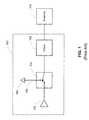
- the antenna 110is sometimes coupled to multiple circuits each comprising a switch 120 , power amplifier 130 , and receiver amplifier 140 , where each such circuit is dedicated to a particular frequency band.
- the transceiver 100handles one or more high bands and/or one or more low bands, for example.
- the filters 150selectively remove frequencies outside of the particular frequency band to which the circuit is dedicated.
- Exemplary articles of manufacture of the present inventioncomprise semiconductor devices, transceivers, and communication devices.
- the articles of manufactureare implemented entirely on silicon substrates using Complementary Metal Oxide Semiconductor (CMOS) technologies.
- An exemplary article of manufacturecomprises a power amplifier, a receiver amplifier, and first and second transmission lines.
- the first transmission lineextends between the power amplifier and an antenna port, and the second transmission line extends between the receiver amplifier and the antenna port.
- the exemplary embodimentalso comprises first and second valves.
- the first valveis configured to change an impedance of the first transmission line and the second valve is configured to change an impedance of the second transmission line.
- the first and second valvesare controllable such that when one is open the other is closed.
- the article of manufactureadditionally comprises control logic configured to oppositely control the first and second valves.
- the article of manufacturecomprises a communications device, for example, the article of manufacture can further comprise an antenna coupled to the antenna port.
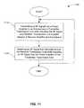
- the present inventionalso provides methods for alternately sending and receiving with an antenna.
- An exemplary methodcomprises alternatingly transmitting RF signals from a power amplifier to an antenna and receiving RF signals from the antenna. More specifically, the step of transmitting the RF signals from the power amplifier to the antenna is performed over a transmitter transmission line while simultaneously impeding the RF signals on a receiver transmission line coupled between the receiver amplifier and the antenna. Similarly, the step of receiving RF signals from the antenna is performed over the receiver transmission line while simultaneously impeding RF signals from the power amplifier on the transmitter transmission line.
- a CMOS deviceswitches from the power amplifier transmitting RF signals to the antenna over the transmitter transmission line to the receiver amplifier receiving RF signals from the antenna over the receiver transmission line.
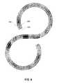
- FIG. 6is a schematic representation of a layout of the line segments of a valve according to still another exemplary embodiment of the invention.
- FIG. 11is a flowchart representation of a method for sending and receiving signals according to an exemplary embodiment of the invention.
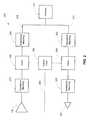
- the device 200can additionally include further valves and amplifiers in parallel to the ones shown in FIG. 2 to handle multiple frequency bands.
- a high band and a low bandcan be accommodated by two power amplifiers 130 and two receiver amplifiers 140 , each amplifier having a dedicated transmission line to the antenna 110 and each dedicated transmission line controlled by a dedicated valve.
- the switchis connecting the antenna port (in many modern cases, the antenna is printed on the circuit board or on a specific substrate mounted on the circuit board) on one side to the input of the low noise amplifier of the receiver in one position or the output of power amplifier in the other position.
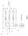
- the current flowing through transmission line 310is about half of the current received by the valve 300 , while the currents in each of the lines 330 , 350 are about one quarter of the current received by the valve 300 .
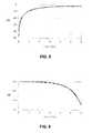
- the valve 300has an insertion loss of less than 0.5 dB.
- any path length difference between the distances from the node 370 to the segments 340 , 360should be an integer multiple of the wavelength so that phase is maintained along the segments 340 , 360 .
- FIG. 5Another exemplary portion of a valve is shown in FIG. 5 .
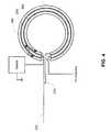
- the line segments 320 , 340 , 360comprise stacked circular arcs with the line segments 340 and 360 disposed along the transmission line segment 320 by being above and below the transmission line segment 320 .
- the line segments 320 , 340 , 360are shown in both a top plan view and in cross-section.
- the top plan viewshows a pair of leads 500 that can be connected to any one of the line segments 320 , 340 , 360 . Connections to the line segments 340 and 360 can alternatively be made through vias.
- the direction of current flow in each of the line segments 320 , 340 , 360are shown in the cross-sectional view.
- the valvewhen the valve is on, RF signals from the power amplifier 130 are significantly attenuated. For additional attenuation, multiple valves can be arranged in series, for example. In some embodiments, the isolation provided at the primary frequency of the power amplifier 130 by a valve that is on is at least 22 dB.
- the transmitter transmission line 210since the transmitter transmission line 210 , even when the valve 230 is on, strongly attenuates frequencies above the frequency of the primary frequency of the power amplifier 130 , articles of manufacture that include the circuitry of FIG. 2 may not include a filter between the power amplifier 130 and the antenna 110 to remove harmonics of the primary frequency.
- the attenuation of the second harmonicis at least 20 dB without such a filter. Higher order harmonics are even more heavily attenuated.
- the attenuation of a third harmoniccan be at least 30 dB in some instances.
Landscapes
- Engineering & Computer Science (AREA)
- Computer Networks & Wireless Communication (AREA)
- Signal Processing (AREA)
- Amplifiers (AREA)
- Transceivers (AREA)
Abstract
Description
Claims (9)
Priority Applications (8)
| Application Number | Priority Date | Filing Date | Title |
|---|---|---|---|
| US12/771,339US8532584B2 (en) | 2010-04-30 | 2010-04-30 | RF switches |
| PCT/US2011/032488WO2011136936A1 (en) | 2010-04-30 | 2011-04-14 | Rf switches |
| CN201180018327.6ACN102859888B (en) | 2010-04-30 | 2011-04-14 | RF switch |
| KR1020127028462AKR101345975B1 (en) | 2010-04-30 | 2011-04-14 | Rf switches |
| EP11775433.3AEP2564513B1 (en) | 2010-04-30 | 2011-04-14 | Rf switches |
| JP2013508002AJP2013526214A (en) | 2010-04-30 | 2011-04-14 | RF (radio frequency) switch |
| TW100114507ATWI496424B (en) | 2010-04-30 | 2011-04-26 | Switching device and method |
| US13/946,892US8731485B2 (en) | 2010-04-30 | 2013-07-19 | RF switches |
Applications Claiming Priority (1)
| Application Number | Priority Date | Filing Date | Title |
|---|---|---|---|
| US12/771,339US8532584B2 (en) | 2010-04-30 | 2010-04-30 | RF switches |
Related Child Applications (1)
| Application Number | Title | Priority Date | Filing Date |
|---|---|---|---|
| US13/946,892ContinuationUS8731485B2 (en) | 2010-04-30 | 2013-07-19 | RF switches |
Publications (2)
| Publication Number | Publication Date |
|---|---|
| US20110269419A1 US20110269419A1 (en) | 2011-11-03 |
| US8532584B2true US8532584B2 (en) | 2013-09-10 |
Family
ID=44858618
Family Applications (2)
| Application Number | Title | Priority Date | Filing Date |
|---|---|---|---|
| US12/771,339Active2032-04-23US8532584B2 (en) | 2010-04-30 | 2010-04-30 | RF switches |
| US13/946,892ActiveUS8731485B2 (en) | 2010-04-30 | 2013-07-19 | RF switches |
Family Applications After (1)
| Application Number | Title | Priority Date | Filing Date |
|---|---|---|---|
| US13/946,892ActiveUS8731485B2 (en) | 2010-04-30 | 2013-07-19 | RF switches |
Country Status (7)
| Country | Link |
|---|---|
| US (2) | US8532584B2 (en) |
| EP (1) | EP2564513B1 (en) |
| JP (1) | JP2013526214A (en) |
| KR (1) | KR101345975B1 (en) |
| CN (1) | CN102859888B (en) |
| TW (1) | TWI496424B (en) |
| WO (1) | WO2011136936A1 (en) |
Cited By (1)
| Publication number | Priority date | Publication date | Assignee | Title |
|---|---|---|---|---|
| US20130303093A1 (en)* | 2010-04-30 | 2013-11-14 | Acco Semiconductor, Inc. | RF Switches |
Families Citing this family (6)
| Publication number | Priority date | Publication date | Assignee | Title |
|---|---|---|---|---|
| US20140179241A1 (en)* | 2012-12-20 | 2014-06-26 | Qualcomm Incorporated | Concurrent matching network using transmission lines for low loss |
| CN107017913B (en)* | 2017-04-14 | 2019-05-17 | 上海晶曦微电子科技有限公司 | A kind of RF transmit-receive circuit |
| KR102006196B1 (en)* | 2017-11-27 | 2019-08-01 | 충남대학교산학협력단 | Radio frequency switch apparatus |
| KR102434773B1 (en) | 2018-03-06 | 2022-08-22 | 삼성전자 주식회사 | Antenna structure and electronic device including the same |
| WO2020035634A1 (en)* | 2018-08-17 | 2020-02-20 | Teknologian Tutkimuskeskus Vtt Oy | Differential transmission line based switch for palna transceivers |
| CN114157332B (en)* | 2021-12-15 | 2023-09-15 | 江苏德是和通信科技有限公司 | Antenna switch board integrating electric switching function |
Citations (61)
| Publication number | Priority date | Publication date | Assignee | Title |
|---|---|---|---|---|
| US4255714A (en) | 1979-02-21 | 1981-03-10 | Rca Corporation | GaAs Dual-gate FET frequency discriminator |
| US4353036A (en) | 1980-08-29 | 1982-10-05 | Rca Corporation | Field effect transistor amplifier with variable gain control |
| US4523111A (en) | 1983-03-07 | 1985-06-11 | General Electric Company | Normally-off, gate-controlled electrical circuit with low on-resistance |
| US4811075A (en) | 1987-04-24 | 1989-03-07 | Power Integrations, Inc. | High voltage MOS transistors |
| US5061903A (en) | 1990-02-27 | 1991-10-29 | Grumman Aerospace Corporation | High voltage modified cascode circuit |
| US5126807A (en) | 1990-06-13 | 1992-06-30 | Kabushiki Kaisha Toshiba | Vertical MOS transistor and its production method |
| US5559049A (en) | 1994-07-25 | 1996-09-24 | Hyundai Electronics Insustries Co., Ltd | Method of manufacturing a semiconductor device |
| US5677927A (en) | 1994-09-20 | 1997-10-14 | Pulson Communications Corporation | Ultrawide-band communication system and method |
| US5898198A (en) | 1997-08-04 | 1999-04-27 | Spectrian | RF power device having voltage controlled linearity |
| US5912490A (en) | 1997-08-04 | 1999-06-15 | Spectrian | MOSFET having buried shield plate for reduced gate/drain capacitance |
| US5969582A (en) | 1997-07-03 | 1999-10-19 | Ericsson Inc. | Impedance matching circuit for power amplifier |
| GB2336485A (en) | 1998-04-14 | 1999-10-20 | Roke Manor Research | Monocycle generator for radar transmitter |
| WO1999056311A1 (en) | 1998-04-27 | 1999-11-04 | Spectrian, Inc. | Mos transistor with shield coplanar with gate electrode |
| US6061008A (en) | 1997-12-19 | 2000-05-09 | Rockwell Science Center, Inc. | Sigma-delta-sigma modulator for high performance analog-to-digital and digital-to-analog conversion |
| US6061555A (en) | 1998-10-21 | 2000-05-09 | Parkervision, Inc. | Method and system for ensuring reception of a communications signal |
| US6081159A (en) | 1998-05-23 | 2000-06-27 | Electronics And Telecommunications Research Institute | Apparatus for improving linearity of small signal |
| US6088484A (en) | 1996-11-08 | 2000-07-11 | Hughes Electronics Corporation | Downloading of personalization layers for symbolically compressed objects |
| WO2001039451A1 (en) | 1999-11-29 | 2001-05-31 | Multispectral Solutions, Inc. | Ultra-wideband data transmission system |
| US6242978B1 (en) | 1999-06-30 | 2001-06-05 | Harris Corporation | Method and apparatus for linearizing an amplifier |
| US6275177B1 (en) | 1999-05-20 | 2001-08-14 | Industrial Technology Research Institute | Sigma-delta modulator using a local nonlinear feedback loop technique |
| IL125022A (en) | 1998-06-21 | 2001-09-13 | Israel Bar David | Methods and apparatus for adaptive adjustment of feed-forward linearized amplifiers |
| US6300835B1 (en) | 1999-12-10 | 2001-10-09 | Motorola, Inc. | Power amplifier core |
| US6304608B1 (en) | 1998-11-04 | 2001-10-16 | Tai-Haur Kuo | Multibit sigma-delta converters employing dynamic element matching with reduced baseband tones |
| US6384688B1 (en) | 1998-07-08 | 2002-05-07 | Hitachi, Ltd. | High-frequency power amplifier module |
| US6414545B1 (en) | 1997-06-27 | 2002-07-02 | The Whitaker Corporation | Predistortion to improve linearity of an amplifier |
| US20020094795A1 (en) | 2001-01-18 | 2002-07-18 | Motorola, Inc. | High efficiency wideband linear wireless power amplifier |
| US20020093442A1 (en) | 2001-01-12 | 2002-07-18 | Broadcom Corporation | Gain scaling for higher signal-to-noise ratios in multistage, multi-bit delta sigma modulators |
| US6570518B2 (en) | 2000-01-07 | 2003-05-27 | Skyworks Solutions, Inc. | Multiple stage delta sigma modulator |
| US6633195B2 (en) | 1999-01-22 | 2003-10-14 | Siemens Aktiengesellschaft | Hybrid power MOSFET |
| US6703684B2 (en) | 2000-09-21 | 2004-03-09 | Cambridge Semiconductor Limited | Semiconductor device and method of forming a semiconductor device |
| US6784470B2 (en) | 2002-06-05 | 2004-08-31 | Intel Corporation | Buffer, buffer operation and method of manufacture |
| US6967608B1 (en) | 2004-06-25 | 2005-11-22 | Texas Instruments Incorporated | Sigma-delta analog-to-digital converter (ADC) with truncation error cancellation in a multi-bit feedback digital-to-analog converter (DAC) |
| US20050287966A1 (en) | 2004-06-24 | 2005-12-29 | Daisuke Yoshimi | Wireless communication system and semiconductor integrated circuit |
| WO2006009009A1 (en) | 2004-07-15 | 2006-01-26 | Sony Corporation | Color filter and color liquid crystal display device |
| US7049669B2 (en) | 2003-09-15 | 2006-05-23 | Infineon Technologies Ag | LDMOS transistor |
| WO2006054148A1 (en) | 2004-11-16 | 2006-05-26 | Acco | An integrated ultra-wideband (uwb) pulse generator |
| US20060228850A1 (en) | 2005-04-06 | 2006-10-12 | Pang-Yen Tsai | Pattern loading effect reduction for selective epitaxial growth |
| US7162042B2 (en) | 1999-08-26 | 2007-01-09 | American Technology Corporation | Modulator processing for a parametric speaker system |
| US20070018865A1 (en) | 2005-07-20 | 2007-01-25 | Industrial Technology Research Institute | Third order sigma-delta modulator |
| WO2007042850A1 (en) | 2005-10-12 | 2007-04-19 | Acco | Insulated gate field-effet transistor having a dummy gate |
| US20070178856A1 (en) | 2006-01-31 | 2007-08-02 | Mitzlaff James E | Method and apparatus for controlling a supply voltage to a power amplifier |
| US20070182485A1 (en) | 2006-02-03 | 2007-08-09 | Sang-Won Ko | Predistorter for Linearization of Power Amplifier |
| US7259621B2 (en) | 2004-02-09 | 2007-08-21 | Sony Ericsson Mobile Communications Japan, Inc. | Distortion compensating device and power amplifying device with distortion compensating function |
| US7312481B2 (en) | 2004-10-01 | 2007-12-25 | Texas Instruments Incorporated | Reliable high-voltage junction field effect transistor and method of manufacture therefor |
| US20080031382A1 (en) | 2006-08-04 | 2008-02-07 | Ichiro Aoki | Low Distortion Radio Frequency (RF) Limiter |
| US7348826B1 (en) | 2005-03-18 | 2008-03-25 | Qspeed Semiconductor Inc. | Composite field effect transistor |
| US20080079499A1 (en) | 2006-09-28 | 2008-04-03 | Via Technologies, Inc. | Power amplifier and method thereof |
| US7378912B2 (en) | 2005-08-26 | 2008-05-27 | Mitsubishi Denki Kabushiki Kaisha | Cascode connection circuit |
| US20080291069A1 (en) | 2007-05-22 | 2008-11-27 | Matsushita Electric Industrial Co., Ltd. | Delta sigma modulator |
| US20080297386A1 (en) | 2007-05-29 | 2008-12-04 | National Semiconductor Corporation | Sigma-delta modulator with dac resolution less than adc resolution |
| US20090066549A1 (en) | 2004-04-09 | 2009-03-12 | Audioasics A/S | Sigma delta modulator |
| US7522079B1 (en) | 2007-09-06 | 2009-04-21 | National Semiconductor Corporation | Sigma-delta modulator with DAC resolution less than ADC resolution and increased tolerance of non-ideal integrators |
| US7554397B2 (en) | 2006-05-22 | 2009-06-30 | Theta Microelectronics, Inc. | Highly linear low-noise amplifiers |
| US7656229B2 (en) | 2008-01-28 | 2010-02-02 | Qualcomm, Incorporated | Method and apparatus for reducing intermodulation distortion in an electronic device having an amplifier circuit |
| US20100026393A1 (en) | 2008-07-30 | 2010-02-04 | Qualcomm Incorporated | Driver amplifier having a programmable output impedance adjustment circuit |
| US7679448B1 (en) | 2007-08-30 | 2010-03-16 | Pmc-Sierra, Inc. | Continuous wave based bias method and apparatus for minimizing MOS transistor distortion |
| US7750666B2 (en)* | 2008-09-15 | 2010-07-06 | Integrated Device Technology, Inc. | Reduced power differential type termination circuit |
| US7808415B1 (en) | 2009-03-25 | 2010-10-05 | Acco Semiconductor, Inc. | Sigma-delta modulator including truncation and applications thereof |
| US7863645B2 (en) | 2008-02-13 | 2011-01-04 | ACCO Semiconductor Inc. | High breakdown voltage double-gate semiconductor device |
| US7952431B2 (en) | 2009-08-28 | 2011-05-31 | Acco Semiconductor, Inc. | Linearization circuits and methods for power amplification |
| US7969243B2 (en) | 2009-04-22 | 2011-06-28 | Acco Semiconductor, Inc. | Electronic circuits including a MOSFET and a dual-gate JFET |
Family Cites Families (27)
| Publication number | Priority date | Publication date | Assignee | Title |
|---|---|---|---|---|
| GB872776A (en)* | 1956-10-11 | 1961-07-12 | Emi Ltd | Improvements relating to variable d.c. transformer circuits |
| JPS56165350A (en) | 1980-05-26 | 1981-12-18 | Hitachi Ltd | Semiconductor device and manufacture thereof |
| US4467296A (en)* | 1982-08-23 | 1984-08-21 | Loral Corporation | Integrated electronic controlled diode filter microwave networks |
| US4841466A (en) | 1987-08-24 | 1989-06-20 | Rca Licensing Corporation | Bit-serial integrator circuitry |
| JPH0399466A (en) | 1989-09-12 | 1991-04-24 | Fujitsu Ltd | Semiconductor device and its manufacturing method |
| US5296400A (en) | 1991-12-14 | 1994-03-22 | Hyundai Electronics Industries Co., Ltd. | Method of manufacturing a contact of a highly integrated semiconductor device |
| US6529451B2 (en) | 1992-10-05 | 2003-03-04 | Mitsubishi Denki Kabushiki Kaisha | Optical disk and optical disk drive device |
| JPH06189524A (en)* | 1992-12-17 | 1994-07-08 | Toshiba Corp | Semiconductor valve |
| JPH10107214A (en) | 1996-10-01 | 1998-04-24 | Masashi Mukogawa | Semiconductor device |
| US6312997B1 (en) | 1998-08-12 | 2001-11-06 | Micron Technology, Inc. | Low voltage high performance semiconductor devices and methods |
| JP3583304B2 (en)* | 1998-11-18 | 2004-11-04 | 松下電器産業株式会社 | Communication terminal device, base station device, and transmission antenna switching method |
| US6222764B1 (en) | 1999-12-13 | 2001-04-24 | Agere Systems Guardian Corp. | Erasable memory device and an associated method for erasing a memory cell therein |
| JP2002305300A (en) | 2001-04-05 | 2002-10-18 | Oki Electric Ind Co Ltd | Power MOS transistor |
| US7796969B2 (en) | 2001-10-10 | 2010-09-14 | Peregrine Semiconductor Corporation | Symmetrically and asymmetrically stacked transistor group RF switch |
| US6804502B2 (en) | 2001-10-10 | 2004-10-12 | Peregrine Semiconductor Corporation | Switch circuit and method of switching radio frequency signals |
| US6600369B2 (en) | 2001-12-07 | 2003-07-29 | Motorola, Inc. | Wideband linear amplifier with predistortion error correction |
| US7138690B2 (en) | 2003-07-21 | 2006-11-21 | Agere Systems Inc. | Shielding structure for use in a metal-oxide-semiconductor device |
| JP2005348206A (en)* | 2004-06-04 | 2005-12-15 | Matsushita Electric Ind Co Ltd | High frequency switch circuit and semiconductor device using the same |
| US7148540B2 (en) | 2004-06-28 | 2006-12-12 | Agere Systems Inc. | Graded conductive structure for use in a metal-oxide-semiconductor device |
| JP4899219B2 (en)* | 2005-01-17 | 2012-03-21 | エスティー‐エリクソン、ソシエテ、アノニム | Modular switching device |
| US7910993B2 (en) | 2005-07-11 | 2011-03-22 | Peregrine Semiconductor Corporation | Method and apparatus for use in improving linearity of MOSFET's using an accumulated charge sink |
| JP4245073B2 (en)* | 2005-08-26 | 2009-03-25 | 株式会社村田製作所 | High frequency switch |
| US7411231B2 (en) | 2005-12-22 | 2008-08-12 | Analog Devices, Inc. | JFET with drain and/or source modification implant |
| US7417515B2 (en)* | 2006-05-15 | 2008-08-26 | Jaalaa, Inc. | On-chip TX/RX antenna switching |
| DE102006045312B3 (en) | 2006-09-26 | 2008-05-21 | Siced Electronics Development Gmbh & Co. Kg | Semiconductor device with coupled junction field effect transistors |
| FR2931300B1 (en) | 2008-05-16 | 2016-10-21 | Thales Sa | HYPERFREQUENCY SWITCH AND TRANSMITTING AND RECEIVING MODULE HAVING SUCH A SWITCH |
| US8532584B2 (en)* | 2010-04-30 | 2013-09-10 | Acco Semiconductor, Inc. | RF switches |
- 2010
- 2010-04-30USUS12/771,339patent/US8532584B2/enactiveActive
- 2011
- 2011-04-14KRKR1020127028462Apatent/KR101345975B1/ennot_activeExpired - Fee Related
- 2011-04-14JPJP2013508002Apatent/JP2013526214A/ennot_activeWithdrawn
- 2011-04-14CNCN201180018327.6Apatent/CN102859888B/ennot_activeExpired - Fee Related
- 2011-04-14WOPCT/US2011/032488patent/WO2011136936A1/enactiveApplication Filing
- 2011-04-14EPEP11775433.3Apatent/EP2564513B1/ennot_activeNot-in-force
- 2011-04-26TWTW100114507Apatent/TWI496424B/ennot_activeIP Right Cessation
- 2013
- 2013-07-19USUS13/946,892patent/US8731485B2/enactiveActive
Patent Citations (63)
| Publication number | Priority date | Publication date | Assignee | Title |
|---|---|---|---|---|
| US4255714A (en) | 1979-02-21 | 1981-03-10 | Rca Corporation | GaAs Dual-gate FET frequency discriminator |
| US4353036A (en) | 1980-08-29 | 1982-10-05 | Rca Corporation | Field effect transistor amplifier with variable gain control |
| US4523111A (en) | 1983-03-07 | 1985-06-11 | General Electric Company | Normally-off, gate-controlled electrical circuit with low on-resistance |
| US4811075A (en) | 1987-04-24 | 1989-03-07 | Power Integrations, Inc. | High voltage MOS transistors |
| US5061903A (en) | 1990-02-27 | 1991-10-29 | Grumman Aerospace Corporation | High voltage modified cascode circuit |
| US5126807A (en) | 1990-06-13 | 1992-06-30 | Kabushiki Kaisha Toshiba | Vertical MOS transistor and its production method |
| US5559049A (en) | 1994-07-25 | 1996-09-24 | Hyundai Electronics Insustries Co., Ltd | Method of manufacturing a semiconductor device |
| US5677927A (en) | 1994-09-20 | 1997-10-14 | Pulson Communications Corporation | Ultrawide-band communication system and method |
| US6088484A (en) | 1996-11-08 | 2000-07-11 | Hughes Electronics Corporation | Downloading of personalization layers for symbolically compressed objects |
| US6414545B1 (en) | 1997-06-27 | 2002-07-02 | The Whitaker Corporation | Predistortion to improve linearity of an amplifier |
| US5969582A (en) | 1997-07-03 | 1999-10-19 | Ericsson Inc. | Impedance matching circuit for power amplifier |
| US5898198A (en) | 1997-08-04 | 1999-04-27 | Spectrian | RF power device having voltage controlled linearity |
| US5912490A (en) | 1997-08-04 | 1999-06-15 | Spectrian | MOSFET having buried shield plate for reduced gate/drain capacitance |
| US6061008A (en) | 1997-12-19 | 2000-05-09 | Rockwell Science Center, Inc. | Sigma-delta-sigma modulator for high performance analog-to-digital and digital-to-analog conversion |
| GB2336485A (en) | 1998-04-14 | 1999-10-20 | Roke Manor Research | Monocycle generator for radar transmitter |
| WO1999056311A1 (en) | 1998-04-27 | 1999-11-04 | Spectrian, Inc. | Mos transistor with shield coplanar with gate electrode |
| US6081159A (en) | 1998-05-23 | 2000-06-27 | Electronics And Telecommunications Research Institute | Apparatus for improving linearity of small signal |
| IL125022A (en) | 1998-06-21 | 2001-09-13 | Israel Bar David | Methods and apparatus for adaptive adjustment of feed-forward linearized amplifiers |
| US6384688B1 (en) | 1998-07-08 | 2002-05-07 | Hitachi, Ltd. | High-frequency power amplifier module |
| US6061555A (en) | 1998-10-21 | 2000-05-09 | Parkervision, Inc. | Method and system for ensuring reception of a communications signal |
| US6304608B1 (en) | 1998-11-04 | 2001-10-16 | Tai-Haur Kuo | Multibit sigma-delta converters employing dynamic element matching with reduced baseband tones |
| US6633195B2 (en) | 1999-01-22 | 2003-10-14 | Siemens Aktiengesellschaft | Hybrid power MOSFET |
| US6275177B1 (en) | 1999-05-20 | 2001-08-14 | Industrial Technology Research Institute | Sigma-delta modulator using a local nonlinear feedback loop technique |
| US6242978B1 (en) | 1999-06-30 | 2001-06-05 | Harris Corporation | Method and apparatus for linearizing an amplifier |
| US7162042B2 (en) | 1999-08-26 | 2007-01-09 | American Technology Corporation | Modulator processing for a parametric speaker system |
| WO2001039451A1 (en) | 1999-11-29 | 2001-05-31 | Multispectral Solutions, Inc. | Ultra-wideband data transmission system |
| US6300835B1 (en) | 1999-12-10 | 2001-10-09 | Motorola, Inc. | Power amplifier core |
| US6570518B2 (en) | 2000-01-07 | 2003-05-27 | Skyworks Solutions, Inc. | Multiple stage delta sigma modulator |
| US6703684B2 (en) | 2000-09-21 | 2004-03-09 | Cambridge Semiconductor Limited | Semiconductor device and method of forming a semiconductor device |
| US20020093442A1 (en) | 2001-01-12 | 2002-07-18 | Broadcom Corporation | Gain scaling for higher signal-to-noise ratios in multistage, multi-bit delta sigma modulators |
| US20020094795A1 (en) | 2001-01-18 | 2002-07-18 | Motorola, Inc. | High efficiency wideband linear wireless power amplifier |
| US6784470B2 (en) | 2002-06-05 | 2004-08-31 | Intel Corporation | Buffer, buffer operation and method of manufacture |
| US7049669B2 (en) | 2003-09-15 | 2006-05-23 | Infineon Technologies Ag | LDMOS transistor |
| US7259621B2 (en) | 2004-02-09 | 2007-08-21 | Sony Ericsson Mobile Communications Japan, Inc. | Distortion compensating device and power amplifying device with distortion compensating function |
| US20090066549A1 (en) | 2004-04-09 | 2009-03-12 | Audioasics A/S | Sigma delta modulator |
| US20050287966A1 (en) | 2004-06-24 | 2005-12-29 | Daisuke Yoshimi | Wireless communication system and semiconductor integrated circuit |
| US6967608B1 (en) | 2004-06-25 | 2005-11-22 | Texas Instruments Incorporated | Sigma-delta analog-to-digital converter (ADC) with truncation error cancellation in a multi-bit feedback digital-to-analog converter (DAC) |
| WO2006009009A1 (en) | 2004-07-15 | 2006-01-26 | Sony Corporation | Color filter and color liquid crystal display device |
| US7312481B2 (en) | 2004-10-01 | 2007-12-25 | Texas Instruments Incorporated | Reliable high-voltage junction field effect transistor and method of manufacture therefor |
| WO2006054148A1 (en) | 2004-11-16 | 2006-05-26 | Acco | An integrated ultra-wideband (uwb) pulse generator |
| US7348826B1 (en) | 2005-03-18 | 2008-03-25 | Qspeed Semiconductor Inc. | Composite field effect transistor |
| US20060228850A1 (en) | 2005-04-06 | 2006-10-12 | Pang-Yen Tsai | Pattern loading effect reduction for selective epitaxial growth |
| US20070018865A1 (en) | 2005-07-20 | 2007-01-25 | Industrial Technology Research Institute | Third order sigma-delta modulator |
| US7378912B2 (en) | 2005-08-26 | 2008-05-27 | Mitsubishi Denki Kabushiki Kaisha | Cascode connection circuit |
| US8008731B2 (en) | 2005-10-12 | 2011-08-30 | Acco | IGFET device having a RF capability |
| WO2007042850A1 (en) | 2005-10-12 | 2007-04-19 | Acco | Insulated gate field-effet transistor having a dummy gate |
| US20070178856A1 (en) | 2006-01-31 | 2007-08-02 | Mitzlaff James E | Method and apparatus for controlling a supply voltage to a power amplifier |
| US20070182485A1 (en) | 2006-02-03 | 2007-08-09 | Sang-Won Ko | Predistorter for Linearization of Power Amplifier |
| US7554397B2 (en) | 2006-05-22 | 2009-06-30 | Theta Microelectronics, Inc. | Highly linear low-noise amplifiers |
| US20080031382A1 (en) | 2006-08-04 | 2008-02-07 | Ichiro Aoki | Low Distortion Radio Frequency (RF) Limiter |
| US20080079499A1 (en) | 2006-09-28 | 2008-04-03 | Via Technologies, Inc. | Power amplifier and method thereof |
| US20080291069A1 (en) | 2007-05-22 | 2008-11-27 | Matsushita Electric Industrial Co., Ltd. | Delta sigma modulator |
| US20080297386A1 (en) | 2007-05-29 | 2008-12-04 | National Semiconductor Corporation | Sigma-delta modulator with dac resolution less than adc resolution |
| US7679448B1 (en) | 2007-08-30 | 2010-03-16 | Pmc-Sierra, Inc. | Continuous wave based bias method and apparatus for minimizing MOS transistor distortion |
| US7522079B1 (en) | 2007-09-06 | 2009-04-21 | National Semiconductor Corporation | Sigma-delta modulator with DAC resolution less than ADC resolution and increased tolerance of non-ideal integrators |
| US7656229B2 (en) | 2008-01-28 | 2010-02-02 | Qualcomm, Incorporated | Method and apparatus for reducing intermodulation distortion in an electronic device having an amplifier circuit |
| US7863645B2 (en) | 2008-02-13 | 2011-01-04 | ACCO Semiconductor Inc. | High breakdown voltage double-gate semiconductor device |
| US20100026393A1 (en) | 2008-07-30 | 2010-02-04 | Qualcomm Incorporated | Driver amplifier having a programmable output impedance adjustment circuit |
| US7750666B2 (en)* | 2008-09-15 | 2010-07-06 | Integrated Device Technology, Inc. | Reduced power differential type termination circuit |
| US7808415B1 (en) | 2009-03-25 | 2010-10-05 | Acco Semiconductor, Inc. | Sigma-delta modulator including truncation and applications thereof |
| US7969341B2 (en) | 2009-03-25 | 2011-06-28 | Acco Semiconductor, Inc. | Sigma-delta modulator including truncation and applications thereof |
| US7969243B2 (en) | 2009-04-22 | 2011-06-28 | Acco Semiconductor, Inc. | Electronic circuits including a MOSFET and a dual-gate JFET |
| US7952431B2 (en) | 2009-08-28 | 2011-05-31 | Acco Semiconductor, Inc. | Linearization circuits and methods for power amplification |
Non-Patent Citations (20)
| Title |
|---|
| Azakkour, A. et al., "A new integrated moncycle generator and transmitter for Ultra-wideband (UWB) communications," IEEE Radio Frequency Circuits Symposium, 2005 pp. 79-82. |
| Azakkour, A. et al., "Challenges for a new integrated Ultra-wideband (UWB) source," IEEE, 2003 pp. 433-437. |
| Choi, Y. H. et al., "Gated UWB Pulse Signal Generation," IEEE, 2004 pp. 122-124. |
| Gautier, D., et al., "Improved Delta Sigma Modulators for High Speed Applications," Acco Semiconductors, Mar. 25, 2009. |
| PCT/IB05/003029 Int'l Search Report, Jul. 6, 2006. |
| PCT/IB05/003029 Written Opinion, Mar. 12, 2008. |
| PCT/IB05/003426 Int'l Search Report, Mar. 20, 2006. |
| PCT/IB05/003426 Written Opinion, May 16, 2007. |
| PCT/US10/041985 Int'l Search Report and Written Opinion, Sep. 9, 2010. |
| PCT/US10/27921 Int'l Search Report and Written Opinion, May 10, 2010. |
| PCT/US10/30770 Int'l Search Report and Written Opinion, Jun. 16, 2010. |
| PCT/US11/32488 Int'l Search Report and Written Opinion, Jun. 28, 2011. |
| PCT/US2008/001938 Int'l Search Report and Written Opinion, Jun. 26, 2008. |
| Pocha, Michael D. et al. "Threshold Voltage Controllability in Double-Diffused MOS Transistors," IEEE Transactions on Electronic Devices, vol. ED-21, No. 12, Dec. 1994. |
| U.S. Appl. No. 12/951,958, Denis Masliah, High Breakdown Voltage Double-Gate Semiconductor Device, filed Nov. 22, 2010. |
| U.S. Appl. No. 12/951,972, Denis Masliah, High Breakdown Voltage Double-Gate Semiconductor Device, filed Nov. 22, 2010. |
| U.S. Appl. No. 13/088,684, Sylvain Quack, Linearization Circuits and Methods for Power Amplification, filed Apr. 18, 2011. |
| U.S. Appl. No. 13/107,411, Alexandre G. Bracale, Electronic circuits including a MOSFET and a dual-gate JFET, filed May 13, 2011. |
| U.S. Appl. No. 13/189,342, Denis Masliah, IGFET Device Having a RF Capability, filed Jul. 22, 2011. |
| Vaes,H. M. J. et al., "High Voltage, High Current Lateral Devices," IEDM Technical Digest, 1988, pp. 87-90. |
Cited By (2)
| Publication number | Priority date | Publication date | Assignee | Title |
|---|---|---|---|---|
| US20130303093A1 (en)* | 2010-04-30 | 2013-11-14 | Acco Semiconductor, Inc. | RF Switches |
| US8731485B2 (en)* | 2010-04-30 | 2014-05-20 | Acco Semiconductor, Inc. | RF switches |
Also Published As
| Publication number | Publication date |
|---|---|
| EP2564513B1 (en) | 2017-07-12 |
| US8731485B2 (en) | 2014-05-20 |
| TW201212554A (en) | 2012-03-16 |
| US20130303093A1 (en) | 2013-11-14 |
| TWI496424B (en) | 2015-08-11 |
| US20110269419A1 (en) | 2011-11-03 |
| KR20130090758A (en) | 2013-08-14 |
| KR101345975B1 (en) | 2014-01-02 |
| CN102859888A (en) | 2013-01-02 |
| JP2013526214A (en) | 2013-06-20 |
| WO2011136936A1 (en) | 2011-11-03 |
| EP2564513A1 (en) | 2013-03-06 |
| CN102859888B (en) | 2014-08-27 |
| EP2564513A4 (en) | 2014-06-25 |
Similar Documents
| Publication | Publication Date | Title |
|---|---|---|
| US8731485B2 (en) | RF switches | |
| US9143184B2 (en) | Radio frequency multi-port switches | |
| CN102299702B (en) | Semiconductor device | |
| KR101850769B1 (en) | Switch module, front-end module, and driving method for switch module | |
| US10153803B2 (en) | Receiving circuit, wireless communication module, and wireless communication device | |
| US11349469B2 (en) | High power radio frequency switches with low leakage current and low insertion loss | |
| KR20070116203A (en) | Apparatus, Method and System for CMOS Antenna Switch Using Switch Resonator | |
| Im et al. | A stacked-FET linear SOI CMOS cellular antenna switch with an extremely low-power biasing strategy | |
| US12142809B2 (en) | Bidirectional RF coupler with switchable coupled transmission lines for operation over different frequency bands | |
| Park et al. | A 24–40 GHz differential SPDT switch with an NMOS and PMOS alternating structure and leakage-canceling capacitors | |
| US20170093032A1 (en) | Radio-Frequency Apparatus With Integrated Antenna Control and Associated Methods | |
| US7425876B2 (en) | Antenna switch circuit and high frequency module having the same | |
| KR100533641B1 (en) | Dual band transmitter with filtering coupler | |
| US10756727B2 (en) | Switching circuit and high-frequency module | |
| US7254371B2 (en) | Multi-port multi-band RF switch | |
| JP6466872B2 (en) | Communication circuit | |
| US20240364335A1 (en) | Switch off state isolation | |
| Moon et al. | Asymmetric SPDT Switch with LC Isolation Technique Using 28-nm FD-SOI CMOS Process for 5G FR2 Applications | |
| US11394358B2 (en) | Filter circuit and communication device | |
| JP5192900B2 (en) | Switch semiconductor integrated circuit | |
| JP2002319848A (en) | Semiconductor switch circuit and semiconductor device |
Legal Events
| Date | Code | Title | Description |
|---|---|---|---|
| AS | Assignment | Owner name:ACCO SEMICONDUCTOR, INC., CALIFORNIA Free format text:ASSIGNMENT OF ASSIGNORS INTEREST;ASSIGNOR:MASLIAH, DENIS A.;REEL/FRAME:024318/0647 Effective date:20100413 | |
| STCF | Information on status: patent grant | Free format text:PATENTED CASE | |
| AS | Assignment | Owner name:ACCO, FRANCE Free format text:ASSIGNMENT OF ASSIGNORS INTEREST;ASSIGNOR:ACCO SEMICONDUCTOR INC.;REEL/FRAME:037370/0275 Effective date:20151217 | |
| FPAY | Fee payment | Year of fee payment:4 | |
| AS | Assignment | Owner name:SOMOS SEMICONDUCTOR, FRANCE Free format text:ASSIGNMENT OF ASSIGNORS INTEREST;ASSIGNOR:ACCO;REEL/FRAME:053178/0925 Effective date:20200701 | |
| AS | Assignment | Owner name:STMICROELECTRONICS INTERNATIONAL N.V., NETHERLANDS Free format text:ASSIGNMENT OF ASSIGNORS INTEREST;ASSIGNOR:SOMOS SEMICONDUCTOR SAS;REEL/FRAME:055220/0856 Effective date:20201030 | |
| FEPP | Fee payment procedure | Free format text:ENTITY STATUS SET TO UNDISCOUNTED (ORIGINAL EVENT CODE: BIG.); ENTITY STATUS OF PATENT OWNER: LARGE ENTITY | |
| MAFP | Maintenance fee payment | Free format text:PAYMENT OF MAINTENANCE FEE, 8TH YEAR, LARGE ENTITY (ORIGINAL EVENT CODE: M1552); ENTITY STATUS OF PATENT OWNER: LARGE ENTITY Year of fee payment:8 | |
| MAFP | Maintenance fee payment | Free format text:PAYMENT OF MAINTENANCE FEE, 12TH YEAR, LARGE ENTITY (ORIGINAL EVENT CODE: M1553); ENTITY STATUS OF PATENT OWNER: LARGE ENTITY Year of fee payment:12 |