US8532450B1 - Optical grating and method of manufacture - Google Patents
Optical grating and method of manufactureDownload PDFInfo
- Publication number
- US8532450B1 US8532450B1US12/645,491US64549109AUS8532450B1US 8532450 B1US8532450 B1US 8532450B1US 64549109 AUS64549109 AUS 64549109AUS 8532450 B1US8532450 B1US 8532450B1
- Authority
- US
- United States
- Prior art keywords
- optically transparent
- transparent layer
- layer
- stop layer
- grating
- Prior art date
- Legal status (The legal status is an assumption and is not a legal conclusion. Google has not performed a legal analysis and makes no representation as to the accuracy of the status listed.)
- Active, expires
Links
- 238000000034methodMethods0.000titleclaimsabstractdescription61
- 230000003287optical effectEffects0.000titleclaimsabstractdescription44
- 238000004519manufacturing processMethods0.000titledescription5
- 239000000463materialSubstances0.000claimsabstractdescription21
- BPUBBGLMJRNUCC-UHFFFAOYSA-Noxygen(2-);tantalum(5+)Chemical compound[O-2].[O-2].[O-2].[O-2].[O-2].[Ta+5].[Ta+5]BPUBBGLMJRNUCC-UHFFFAOYSA-N0.000claimsdescription7
- 229910001936tantalum oxideInorganic materials0.000claimsdescription7
- 238000005530etchingMethods0.000claimsdescription5
- TWNQGVIAIRXVLR-UHFFFAOYSA-Noxo(oxoalumanyloxy)alumaneChemical compoundO=[Al]O[Al]=OTWNQGVIAIRXVLR-UHFFFAOYSA-N0.000claimsdescription3
- 239000011295pitchSubstances0.000description30
- 239000011162core materialSubstances0.000description10
- 238000010586diagramMethods0.000description9
- 229920002120photoresistant polymerPolymers0.000description6
- 230000008878couplingEffects0.000description5
- 238000010168coupling processMethods0.000description5
- 238000005859coupling reactionMethods0.000description5
- 230000002411adverseEffects0.000description3
- 238000007796conventional methodMethods0.000description3
- 230000015572biosynthetic processEffects0.000description2
- 238000001228spectrumMethods0.000description2
- 239000000758substrateSubstances0.000description2
- PBCFLUZVCVVTBY-UHFFFAOYSA-Ntantalum pentoxideInorganic materialsO=[Ta](=O)O[Ta](=O)=OPBCFLUZVCVVTBY-UHFFFAOYSA-N0.000description2
- PNEYBMLMFCGWSK-UHFFFAOYSA-Naluminium oxideInorganic materials[O-2].[O-2].[O-2].[Al+3].[Al+3]PNEYBMLMFCGWSK-UHFFFAOYSA-N0.000description1
- 230000005670electromagnetic radiationEffects0.000description1
- 238000007654immersionMethods0.000description1
- 239000000203mixtureSubstances0.000description1
- 239000007787solidSubstances0.000description1
Images


Classifications
- G—PHYSICS
- G02—OPTICS
- G02B—OPTICAL ELEMENTS, SYSTEMS OR APPARATUS
- G02B5/00—Optical elements other than lenses
- G02B5/18—Diffraction gratings
- G02B5/1847—Manufacturing methods
- G02B5/1857—Manufacturing methods using exposure or etching means, e.g. holography, photolithography, exposure to electron or ion beams
Definitions
- Optical gratingsare used for light coupling and delivery in a variety of optical systems.
- electromagnetic radiationis provided from a laser to a grating.
- the light provided from the laseris in the optical range of the spectrum.
- the gratingis configured for a particular wavelength in the spectrum. Typically this means that the grating actually functions in a range of wavelengths around the particular wavelength.
- the gratingcouples light of the particular wavelength from the laser to a waveguide.
- the light from the waveguideis typically provided to a near-field transducer (NFT) and used to heat a spot on a magnetic recording media. Data is magnetically written to the spot while the spot is heated.
- NFTnear-field transducer
- the coupling efficiency of a gratingis a measure of the losses in optical energy between light input to the grating and light output by the grating. A higher coupling efficiency translates to lower losses in the grating. Thus, a higher coupling efficiency is desired.
- the geometry of the gratingsuch as the pitch, depth, and shape of ridges in the grating are closely controlled. Thus, fabrication of a grating includes controls of such features.
- FIG. 1depicts a conventional method 10 for fabricating a conventional grating.
- the core materialssuch as Ta 2 O 5 are deposited, via step 12 .
- a photoresist maskis provided on the core material, via step 14 .
- the photoresist maskhas a series of lines interleaved with apertures.
- the core materialis etched, via step 16 . Thus, the pattern of the photoresist mask is transferred to the core material.
- FIG. 2depicts a conventional grating 50 having a pitch, d.
- the conventional grating 50includes core material 54 on a substrate 52 .
- the core material 54includes a plurality of ridges, such as the ridge 62 , interleaved with troughs, such as the troughs 64 , 66 , and 68 .
- a photoresist mask 56used in fabricating the grating 50 .
- the photoresist mask 56includes lines 58 interleaved with apertures 60 at the pitch, d.
- the geometry of the conventional grating 50may differ from what is desired. More specifically, as can be seen in FIG. 2 , the troughs differ.
- troughs 64 , 66 , and 68differ in width, depth, and profile. Further, the depth of the troughs that are achievable may be limited by the pitch of the conventional grating 50 . Such differences in the troughs may adversely affect performance of the conventional grating 50 . More specifically, the optical efficiency of the conventional grating 50 may degrade.
- the optical gratingis configured for light of a wavelength and includes a first optically transparent layer, a stop layer on the first optically transparent layer, and a second optically transparent layer on the stop layer.
- the first optically transparent layeris continuous and includes a material.
- the second optically transparent layeralso includes the material.
- the second optically transparent layeralso includes a plurality of discrete ridges spaced apart by a pitch.
- the stop layeris configured to be invisible to the light.
- FIG. 1is a flow chart depicting a conventional method for fabricating an optical grating.
- FIG. 2is a diagram depicting a conventional grating.
- FIG. 3is a flow chart depicting an exemplary embodiment of a method for fabricating a grating.
- FIG. 4is a diagram depicting an exemplary embodiment of an optical grating
- FIG. 5is a diagram depicting another exemplary embodiment of an optical grating.
- FIG. 6is a diagram depicting another exemplary embodiment of an optical grating.
- FIG. 7is a flow chart depicting another exemplary embodiment of a method for fabricating an optical grating.
- FIGS. 8-11are diagrams depicting an exemplary embodiment of a grating during fabrication.
- FIG. 3is a flow chart depicting an exemplary embodiment of a method 100 for fabricating a grating. Although certain steps are shown, some steps may be omitted, interleaved, and/or combined.
- the grating being fabricatedmay be used in an optical system such as EAMR head that resides on a slider (not shown) in a disk drive.
- the method 100may be part of a method used in fabricating an EAMR head.
- the method 100also may commence after formation of other portions of the EAMR head.
- the method 100is also described in the context of providing a single grating. However, the method 100 may be used to fabricate multiple gratings at substantially the same time.
- the method 100 and systemare also described in the context of particular layers.
- such layersmay include multiple sub-layers.
- the grating fabricated using the method 100is configured for a particular wavelength.
- the gratingoperates for light in a range around the wavelength.
- the grating being fabricatedis configured for 850 nm light.
- the wavelengthmay differ.
- gratings for wavelengths of nine hundred nanometers or moremight be fabricated.
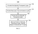
- a first optically transparent layeris provided, via step 102 .
- the optically transparent layermay include materials such as those used for the core of a waveguide.
- the optically transparent layermay include tantalum oxide (e.g. Ta 2 O 5 ).
- the thickness of the first optically transparent layerdepends upon the total thickness of the components to which the light is to be coupled. In some embodiments, the total thickness of the grating is desired to be on the order of one hundred fifty nanometers. Thus, the first optically transparent layer may be at least forty nanometers and not more than eighty nanometers.
- a stop layeris provided on the first optically transparent layer, via step 104 .
- the stop layer provided in step 104is configured to be invisible to the light with which the grating is desired operate. In some embodiments, therefore, the stop layer is not more than ten percent of the wavelength of the light for which the grating is configured. In many embodiments, the stop layer is significantly thinner than ten percent of the wavelength. For example, for a grating configured for 850 nm light, the stop layer may be at least one and not more than twenty-five nanometers. In some such embodiments, the stop layer may be at least one and not more than fifteen nanometers. Thus, the stop layer is sufficiently thin that the stop layer does not adversely affect the performance of the grating. In some embodiments, the stop layer has an index of refraction and a dielectric constant configured to confine the light in at least one of the first optically transparent layer and the second optically transparent layer. In some embodiments, the stop layer includes aluminum oxide.
- a second optically transparent layeris provided on the stop layer, via step 106 .
- the second optically transparent layerincludes the material that is also used in the first optically transparent layer.
- the second optically transparent layer provided in step 106may include core materials such as tantalum oxide.
- the second optically transparent layerconsists of the material.
- the first and second optically transparent layersmay have identical compositions.
- the second optically transparent layermay also have a thickness desired for the ridges of the grating being formed. In some embodiments, the thickness of the second optically transparent layer is at least fifty and not more than one hundred nanometers.
- Step 108may include forming a mask having lines interleaved with apertures, then etching the second optically transparent layer with the mask in place. Thus, a plurality of discrete ridges interleaved with a plurality of troughs are formed in the second optically transparent layer.
- the discrete ridgesspaced apart by a pitch. In some embodiments, the pitch is constant throughout the grating. In other embodiments, the pitch varies across the grating. Thus, a nonlinear grating may be formed. Because of the presence of the stop layer, the ridges formed by the removal process in step 108 have a maximum height substantially the same as the thickness of the second optically transparent layer.
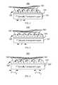
- FIG. 4is a diagram depicting an exemplary embodiment of an optical grating 150 formed using the method 100 .
- the optical grating 150includes a first optically transparent layer 152 , a stop layer 154 , and a second optically transparent layer 156 .
- the second optically transparent layer 156has been etched to form a series of ridges 158 interleaved with troughs 160 .
- the troughs 160are depicted as extending through the second optically transparent layer 156 to the stop layer 154 . However, in some embodiments, the troughs 160 may terminate in another layer, for example within the second optically transparent layer 156 .
- the grating 150has a pitch, d, that is constant across the grating 150 .
- FIG. 5is a diagram depicting an exemplary embodiment of an optical grating 150 ′ formed using the method 100 .
- the grating 150 ′is analogous to the grating 150 . Consequently, analogous components are labeled similarly.
- the optical grating 150 ′thus includes a first optically transparent layer 152 ′, a stop layer 154 ′, and a second optically transparent layer 156 ′ having ridges 158 ′ interleaved with troughs 160 ′.
- the troughs 160 ′are depicted as extending through the second optically transparent layer 156 ′ to the stop layer 154 ′.
- the troughs 160 ′may terminate in another layer, for example within the second optically transparent layer 156 ′.
- the grating 150 ′has a pitch d′ different from that of the grating 150 .
- the heights of the ridges 158 ′are substantially the same as for the ridges 158 of the grating 150 .
- FIG. 6is a diagram depicting an exemplary embodiment of an optical grating 150 ′′ that is also formed using the method 100 .
- the grating 150 ′′is analogous to the grating 150 . Consequently, analogous components are labeled similarly.
- the optical grating 150 ′′thus includes a first optically transparent layer 152 ′′, a stop layer 154 ′′, and a second optically transparent layer 156 ′′ having ridges 158 ′′ interleaved with troughs 160 ′′.
- the troughs 160 ′′are depicted as extending through the second optically transparent layer 156 ′′ to the stop layer 154 ′′.
- the troughs 160 ′′may terminate in another layer, for example within the second optically transparent layer 156 ′′.
- the pitchmay vary in another manner.
- gratings 150 / 150 ′/ 150 ′′may be provided. More specifically, the method 100 decouples the pitch of the gratings 150 / 150 ′/ 150 ′′ from the height of the ridges 158 / 158 ′/ 158 ′′. The pitch is also decoupled from the depths of the troughs 160 / 160 ′/ 160 ′′. The maximum height of the ridges 158 / 158 ′/ 158 ′′ may be controlled by the thickness of the second optically transparent layer 156 / 156 ′/ 156 ′′ and thus the position of the stop layer 154 / 154 ′/ 154 ′′.
- the pitchis controlled by the distance between apertures in a mask used in step 108 .
- gratings 150 / 150 ′/ 150 ′′ having the same height of the ridges 158 / 158 ′/ 158 ′′may have different pitches d, d′, and d′′, respectively.
- a nonlinear grating 150 ′′ having a varying pitchmay also be provided.
- the flexibility of the gratings 150 / 150 ′/ 150 ′′ provided via the method 100may be improved.
- the geometries of the gratings 150 / 150 ′/ 150 ′′are closer to that which is desired for a particular wavelength.
- the method 100results in gratings 150 / 150 ′/ 150 ′′ that may have improved optical efficiency.
- This flexibility and improved optical efficiencymay be provided without the stop layer 154 / 154 ′/ 154 ′′ adversely affecting performance of the gratings 150 / 150 ′/ 150 ′′.
- This benefitis provided because the stop layer 154 / 154 ′/ 154 ′′ is configured to be invisible to the light used with the gratings 150 / 150 ′/ 150 ′′.
- the stop layer 154 / 154 ′/ 154 ′′is a stop for the removal process that forms the ridges 158 / 158 ′/ 158 ′′ and troughs 160 / 160 ′/ 160 ′′
- the yield for the method 100may be improved.
- manufacturability as well as performance of the gratings 150 / 150 ′/ 150 ′′may be improved.
- the method 100may be extended to other optical components. For example, channel waveguides, optical mode converters, tapered waveguides and solid immersion mirrors are among the components that might be so fabricated.
- structures of a stop layer sandwiched between optically transparent layers and use of the removal of an outer layer terminated by the stop layermay provide the desired geometry of the structure being formed.
- FIG. 7is a flow chart depicting another exemplary embodiment of a method 200 for fabricating an optical grating. Although certain steps are shown, some steps may be omitted, interleaved, or combined.
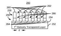
- FIGS. 8-11are diagrams depicting side views of an exemplary embodiment of a portion of an optical grating 250 during fabrication. For clarity, FIGS. 8-11 are not to scale. Referring to FIGS. 7-11 , the method 200 is described in the context of the grating 250 . However, the method 200 may be used to form another device (not shown). Further, the method 200 may be part of another method used in forming an EAMR head. The method 200 may thus commence after formation of other portions of the EAMR transducer of which the grating 250 is part.
- the method 200is also described in the context of providing a single grating 250 .
- the method 200may be used to fabricate multiple gratings at substantially the same time.
- the method 200 and grating 250are also described in the context of particular layers. However, in some embodiments, such layers may include multiple sublayers.
- the grating fabricated using the method 200is configured for a particular wavelength. Thus, the grating operates for light in a range around the wavelength. For example, in one embodiment, the grating being fabricated is configured for 850 nm light. In other embodiments, the wavelength may be different.
- a first optically transparent layeris provided, via step 202 .
- the optically transparent layermay include materials such as those used for the core of a waveguide.
- the optically transparent layermay include tantalum oxide.
- the thickness of the first optically transparent layerdepends upon the total thickness of the components to which the light is to be coupled.
- a stop layeris provided on the first optically transparent layer, via step 204 .
- the stop layeris a stop for a removal process, described below.
- the stop layerincludes alumina.
- the stop layer provided in step 204is also desired to leave performance of the grating being formed substantially unaffected.
- the stop layeris configured to be invisible to the light with which the grating is desired operate.
- the stop layerhas an index of refraction and a dielectric constant configured to confine the light in at least one of the first optically transparent layer and the second optically transparent layer.
- the index of refraction of the stop layermay be approximately 1.65.
- a second optically transparent layeris provided on the stop layer, via step 206 .
- the second optically transparent layerincludes the material that is also used in the first optically transparent layer.
- the second optically transparent layer provided in step 206may include core materials such as tantalum oxide.
- the first optically transparent layer and the second optically transparent layerconsists of the material.
- both the first optically transparent layer and the second optically transparent layermay consist of tantalum oxide.
- FIG. 8depicts the grating 250 after step 206 is performed.
- the first optically transparent layer 252 , the stop layer 254 , and the second optically transparent layer 256are shown. Not shown are layers under the first optically transparent layer 252 , such as a substrate or other structures.
- the first optically transparent layermay be at least forty nanometers and not more than eighty nanometers.
- the stop layer 254is configured to be invisible to the light with which the grating 250 is desired operate. In some embodiments, therefore, the stop layer 254 is not more than ten percent of the wavelength of the light for which the grating 250 is configured. In many embodiments, the stop layer 254 is significantly thinner than ten percent of the wavelength.
- the stop layer 254may be at least one and not more than twenty-five nanometers. In some embodiments, the stop layer 254 may be at least one and not more than fifteen nanometers. In some such embodiments, the stop layer 254 is at least nine and not more than eleven nanometers thick. In some embodiments, the thickness of the second optically transparent layer 256 is substantially the same as the height of the ridges to be formed in the grating 250 . In some embodiments, the thickness of the second optically transparent layer 256 is at least fifty nanometers and not more than one hundred nanometers.
- a mask including a plurality of lines interspersed with a plurality of aperturesis provided, via step 208 .
- the mask provided in step 208is to be used in fabricating the ridges of the grating, as described below.
- FIG. 9depicts the grating 250 after step 208 is performed.
- the mask 258is shown.
- the mask 258includes lines 260 interleaved with apertures 262 .
- the apertures 262expose a portion of the second optically transparent layer 256 .
- the apertures 262 /lines 260are spaced apart by a pitch, d.
- the pitchis constant across the grating. However, in other embodiments, the pitch may vary across the grating 250 .
- a nonlinear gratingmay also be formed.
- FIG. 10depicts the grating 250 after step 210 is performed.
- the pitch of the ridges 264 /troughs 266 , dis substantially the same as the pitch of the lines 260 /apertures 262 in the mask 258 .
- the pitch of the grating 250 shown in FIGS. 8-11is constant. However, in other embodiments, the pitch may vary. Further, as can be seen in FIG. 10 , the bottoms of the troughs 266 are formed by the stop layer 254 .
- the mask 256is removed, via step 212 .
- a photoresist stripmay be performed in step 212 .
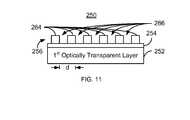
- FIG. 11depicts the grating 250 after step 212 is performed.
- the grating 250 including ridges 264 in the second optically transparent layer 256is formed.
- the first optically transparent layer 252remains continuous. Fabrication of the device may then be completed, via step 214 .
- other structures of the EAMR head or other device incorporating the grating 250may be formed.
- the grating 250may be provided.
- the method 200 and grating 250share the benefits of the method 100 and gratings 150 / 150 ′/ 150 ′′.
- the method 200decouples the spacing between the ridges 264 , or pitch d, from the height of the ridges 264 .
- a variety of gratings 250 having a variety of pitches and improved optical efficiencymay be fabricated.
- the method 200may have improved yield.
Landscapes
- Physics & Mathematics (AREA)
- Engineering & Computer Science (AREA)
- Manufacturing & Machinery (AREA)
- General Physics & Mathematics (AREA)
- Optics & Photonics (AREA)
- Optical Integrated Circuits (AREA)
Abstract
Description
Claims (21)
Priority Applications (1)
| Application Number | Priority Date | Filing Date | Title |
|---|---|---|---|
| US12/645,491US8532450B1 (en) | 2009-12-23 | 2009-12-23 | Optical grating and method of manufacture |
Applications Claiming Priority (1)
| Application Number | Priority Date | Filing Date | Title |
|---|---|---|---|
| US12/645,491US8532450B1 (en) | 2009-12-23 | 2009-12-23 | Optical grating and method of manufacture |
Publications (1)
| Publication Number | Publication Date |
|---|---|
| US8532450B1true US8532450B1 (en) | 2013-09-10 |
Family
ID=49084168
Family Applications (1)
| Application Number | Title | Priority Date | Filing Date |
|---|---|---|---|
| US12/645,491Active2030-12-19US8532450B1 (en) | 2009-12-23 | 2009-12-23 | Optical grating and method of manufacture |
Country Status (1)
| Country | Link |
|---|---|
| US (1) | US8532450B1 (en) |
Cited By (132)
| Publication number | Priority date | Publication date | Assignee | Title |
|---|---|---|---|---|
| US8830628B1 (en) | 2009-02-23 | 2014-09-09 | Western Digital (Fremont), Llc | Method and system for providing a perpendicular magnetic recording head |
| US8879207B1 (en) | 2011-12-20 | 2014-11-04 | Western Digital (Fremont), Llc | Method for providing a side shield for a magnetic recording transducer using an air bridge |
| US8883017B1 (en) | 2013-03-12 | 2014-11-11 | Western Digital (Fremont), Llc | Method and system for providing a read transducer having seamless interfaces |
| US8917581B1 (en) | 2013-12-18 | 2014-12-23 | Western Digital Technologies, Inc. | Self-anneal process for a near field transducer and chimney in a hard disk drive assembly |
| US8923102B1 (en) | 2013-07-16 | 2014-12-30 | Western Digital (Fremont), Llc | Optical grating coupling for interferometric waveguides in heat assisted magnetic recording heads |
| US8947985B1 (en) | 2013-07-16 | 2015-02-03 | Western Digital (Fremont), Llc | Heat assisted magnetic recording transducers having a recessed pole |
| US8953422B1 (en) | 2014-06-10 | 2015-02-10 | Western Digital (Fremont), Llc | Near field transducer using dielectric waveguide core with fine ridge feature |
| US8958272B1 (en) | 2014-06-10 | 2015-02-17 | Western Digital (Fremont), Llc | Interfering near field transducer for energy assisted magnetic recording |
| US8971160B1 (en) | 2013-12-19 | 2015-03-03 | Western Digital (Fremont), Llc | Near field transducer with high refractive index pin for heat assisted magnetic recording |
| US8970988B1 (en) | 2013-12-31 | 2015-03-03 | Western Digital (Fremont), Llc | Electric gaps and method for making electric gaps for multiple sensor arrays |
| US8976635B1 (en) | 2014-06-10 | 2015-03-10 | Western Digital (Fremont), Llc | Near field transducer driven by a transverse electric waveguide for energy assisted magnetic recording |
| US8980109B1 (en) | 2012-12-11 | 2015-03-17 | Western Digital (Fremont), Llc | Method for providing a magnetic recording transducer using a combined main pole and side shield CMP for a wraparound shield scheme |
| US8982508B1 (en) | 2011-10-31 | 2015-03-17 | Western Digital (Fremont), Llc | Method for providing a side shield for a magnetic recording transducer |
| US8988812B1 (en) | 2013-11-27 | 2015-03-24 | Western Digital (Fremont), Llc | Multi-sensor array configuration for a two-dimensional magnetic recording (TDMR) operation |
| US8988825B1 (en) | 2014-02-28 | 2015-03-24 | Western Digital (Fremont, LLC | Method for fabricating a magnetic writer having half-side shields |
| US8984740B1 (en) | 2012-11-30 | 2015-03-24 | Western Digital (Fremont), Llc | Process for providing a magnetic recording transducer having a smooth magnetic seed layer |
| US8995087B1 (en) | 2006-11-29 | 2015-03-31 | Western Digital (Fremont), Llc | Perpendicular magnetic recording write head having a wrap around shield |
| US8993217B1 (en) | 2013-04-04 | 2015-03-31 | Western Digital (Fremont), Llc | Double exposure technique for high resolution disk imaging |
| US9001467B1 (en) | 2014-03-05 | 2015-04-07 | Western Digital (Fremont), Llc | Method for fabricating side shields in a magnetic writer |
| US9001628B1 (en) | 2013-12-16 | 2015-04-07 | Western Digital (Fremont), Llc | Assistant waveguides for evaluating main waveguide coupling efficiency and diode laser alignment tolerances for hard disk |
| US8997832B1 (en) | 2010-11-23 | 2015-04-07 | Western Digital (Fremont), Llc | Method of fabricating micrometer scale components |
| US9007879B1 (en) | 2014-06-10 | 2015-04-14 | Western Digital (Fremont), Llc | Interfering near field transducer having a wide metal bar feature for energy assisted magnetic recording |
| US9007719B1 (en) | 2013-10-23 | 2015-04-14 | Western Digital (Fremont), Llc | Systems and methods for using double mask techniques to achieve very small features |
| US9007725B1 (en) | 2014-10-07 | 2015-04-14 | Western Digital (Fremont), Llc | Sensor with positive coupling between dual ferromagnetic free layer laminates |
| US9013836B1 (en) | 2013-04-02 | 2015-04-21 | Western Digital (Fremont), Llc | Method and system for providing an antiferromagnetically coupled return pole |
| US9042058B1 (en) | 2013-10-17 | 2015-05-26 | Western Digital Technologies, Inc. | Shield designed for middle shields in a multiple sensor array |
| US9042052B1 (en) | 2014-06-23 | 2015-05-26 | Western Digital (Fremont), Llc | Magnetic writer having a partially shunted coil |
| US9042208B1 (en) | 2013-03-11 | 2015-05-26 | Western Digital Technologies, Inc. | Disk drive measuring fly height by applying a bias voltage to an electrically insulated write component of a head |
| US9042057B1 (en) | 2013-01-09 | 2015-05-26 | Western Digital (Fremont), Llc | Methods for providing magnetic storage elements with high magneto-resistance using Heusler alloys |
| US9042051B2 (en) | 2013-08-15 | 2015-05-26 | Western Digital (Fremont), Llc | Gradient write gap for perpendicular magnetic recording writer |
| US9053735B1 (en) | 2014-06-20 | 2015-06-09 | Western Digital (Fremont), Llc | Method for fabricating a magnetic writer using a full-film metal planarization |
| US9064507B1 (en) | 2009-07-31 | 2015-06-23 | Western Digital (Fremont), Llc | Magnetic etch-stop layer for magnetoresistive read heads |
| US9064527B1 (en) | 2013-04-12 | 2015-06-23 | Western Digital (Fremont), Llc | High order tapered waveguide for use in a heat assisted magnetic recording head |
| US9065043B1 (en) | 2012-06-29 | 2015-06-23 | Western Digital (Fremont), Llc | Tunnel magnetoresistance read head with narrow shield-to-shield spacing |
| US9064528B1 (en) | 2013-05-17 | 2015-06-23 | Western Digital Technologies, Inc. | Interferometric waveguide usable in shingled heat assisted magnetic recording in the absence of a near-field transducer |
| US9070381B1 (en) | 2013-04-12 | 2015-06-30 | Western Digital (Fremont), Llc | Magnetic recording read transducer having a laminated free layer |
| US9082423B1 (en) | 2013-12-18 | 2015-07-14 | Western Digital (Fremont), Llc | Magnetic recording write transducer having an improved trailing surface profile |
| US9087527B1 (en) | 2014-10-28 | 2015-07-21 | Western Digital (Fremont), Llc | Apparatus and method for middle shield connection in magnetic recording transducers |
| US9087534B1 (en) | 2011-12-20 | 2015-07-21 | Western Digital (Fremont), Llc | Method and system for providing a read transducer having soft and hard magnetic bias structures |
| US9093639B2 (en) | 2012-02-21 | 2015-07-28 | Western Digital (Fremont), Llc | Methods for manufacturing a magnetoresistive structure utilizing heating and cooling |
| US9104107B1 (en) | 2013-04-03 | 2015-08-11 | Western Digital (Fremont), Llc | DUV photoresist process |
| US9111564B1 (en) | 2013-04-02 | 2015-08-18 | Western Digital (Fremont), Llc | Magnetic recording writer having a main pole with multiple flare angles |
| US9111558B1 (en) | 2014-03-14 | 2015-08-18 | Western Digital (Fremont), Llc | System and method of diffractive focusing of light in a waveguide |
| US9111550B1 (en) | 2014-12-04 | 2015-08-18 | Western Digital (Fremont), Llc | Write transducer having a magnetic buffer layer spaced between a side shield and a write pole by non-magnetic layers |
| US9123359B1 (en) | 2010-12-22 | 2015-09-01 | Western Digital (Fremont), Llc | Magnetic recording transducer with sputtered antiferromagnetic coupling trilayer between plated ferromagnetic shields and method of fabrication |
| US9123362B1 (en) | 2011-03-22 | 2015-09-01 | Western Digital (Fremont), Llc | Methods for assembling an electrically assisted magnetic recording (EAMR) head |
| US9123358B1 (en) | 2012-06-11 | 2015-09-01 | Western Digital (Fremont), Llc | Conformal high moment side shield seed layer for perpendicular magnetic recording writer |
| US9123374B1 (en) | 2015-02-12 | 2015-09-01 | Western Digital (Fremont), Llc | Heat assisted magnetic recording writer having an integrated polarization rotation plate |
| US9135930B1 (en) | 2014-03-06 | 2015-09-15 | Western Digital (Fremont), Llc | Method for fabricating a magnetic write pole using vacuum deposition |
| US9135937B1 (en) | 2014-05-09 | 2015-09-15 | Western Digital (Fremont), Llc | Current modulation on laser diode for energy assisted magnetic recording transducer |
| US9142233B1 (en) | 2014-02-28 | 2015-09-22 | Western Digital (Fremont), Llc | Heat assisted magnetic recording writer having a recessed pole |
| US9147408B1 (en) | 2013-12-19 | 2015-09-29 | Western Digital (Fremont), Llc | Heated AFM layer deposition and cooling process for TMR magnetic recording sensor with high pinning field |
| US9147404B1 (en) | 2015-03-31 | 2015-09-29 | Western Digital (Fremont), Llc | Method and system for providing a read transducer having a dual free layer |
| US9153255B1 (en) | 2014-03-05 | 2015-10-06 | Western Digital (Fremont), Llc | Method for fabricating a magnetic writer having an asymmetric gap and shields |
| US9183854B2 (en) | 2014-02-24 | 2015-11-10 | Western Digital (Fremont), Llc | Method to make interferometric taper waveguide for HAMR light delivery |
| US9190079B1 (en) | 2014-09-22 | 2015-11-17 | Western Digital (Fremont), Llc | Magnetic write pole having engineered radius of curvature and chisel angle profiles |
| US9190085B1 (en) | 2014-03-12 | 2015-11-17 | Western Digital (Fremont), Llc | Waveguide with reflective grating for localized energy intensity |
| US9194692B1 (en) | 2013-12-06 | 2015-11-24 | Western Digital (Fremont), Llc | Systems and methods for using white light interferometry to measure undercut of a bi-layer structure |
| US9202480B2 (en) | 2009-10-14 | 2015-12-01 | Western Digital (Fremont), LLC. | Double patterning hard mask for damascene perpendicular magnetic recording (PMR) writer |
| US9202493B1 (en) | 2014-02-28 | 2015-12-01 | Western Digital (Fremont), Llc | Method of making an ultra-sharp tip mode converter for a HAMR head |
| US9214172B2 (en) | 2013-10-23 | 2015-12-15 | Western Digital (Fremont), Llc | Method of manufacturing a magnetic read head |
| US9214165B1 (en) | 2014-12-18 | 2015-12-15 | Western Digital (Fremont), Llc | Magnetic writer having a gradient in saturation magnetization of the shields |
| US9214169B1 (en) | 2014-06-20 | 2015-12-15 | Western Digital (Fremont), Llc | Magnetic recording read transducer having a laminated free layer |
| US9213322B1 (en) | 2012-08-16 | 2015-12-15 | Western Digital (Fremont), Llc | Methods for providing run to run process control using a dynamic tuner |
| US9230565B1 (en) | 2014-06-24 | 2016-01-05 | Western Digital (Fremont), Llc | Magnetic shield for magnetic recording head |
| US9236560B1 (en) | 2014-12-08 | 2016-01-12 | Western Digital (Fremont), Llc | Spin transfer torque tunneling magnetoresistive device having a laminated free layer with perpendicular magnetic anisotropy |
| US9245543B1 (en) | 2010-06-25 | 2016-01-26 | Western Digital (Fremont), Llc | Method for providing an energy assisted magnetic recording head having a laser integrally mounted to the slider |
| US9245545B1 (en) | 2013-04-12 | 2016-01-26 | Wester Digital (Fremont), Llc | Short yoke length coils for magnetic heads in disk drives |
| US9245562B1 (en) | 2015-03-30 | 2016-01-26 | Western Digital (Fremont), Llc | Magnetic recording writer with a composite main pole |
| US9251813B1 (en) | 2009-04-19 | 2016-02-02 | Western Digital (Fremont), Llc | Method of making a magnetic recording head |
| US9263071B1 (en) | 2015-03-31 | 2016-02-16 | Western Digital (Fremont), Llc | Flat NFT for heat assisted magnetic recording |
| US9263067B1 (en) | 2013-05-29 | 2016-02-16 | Western Digital (Fremont), Llc | Process for making PMR writer with constant side wall angle |
| US9269382B1 (en) | 2012-06-29 | 2016-02-23 | Western Digital (Fremont), Llc | Method and system for providing a read transducer having improved pinning of the pinned layer at higher recording densities |
| US9275657B1 (en) | 2013-08-14 | 2016-03-01 | Western Digital (Fremont), Llc | Process for making PMR writer with non-conformal side gaps |
| US9280990B1 (en) | 2013-12-11 | 2016-03-08 | Western Digital (Fremont), Llc | Method for fabricating a magnetic writer using multiple etches |
| US9287494B1 (en) | 2013-06-28 | 2016-03-15 | Western Digital (Fremont), Llc | Magnetic tunnel junction (MTJ) with a magnesium oxide tunnel barrier |
| US9286919B1 (en) | 2014-12-17 | 2016-03-15 | Western Digital (Fremont), Llc | Magnetic writer having a dual side gap |
| US9305583B1 (en) | 2014-02-18 | 2016-04-05 | Western Digital (Fremont), Llc | Method for fabricating a magnetic writer using multiple etches of damascene materials |
| US9312064B1 (en) | 2015-03-02 | 2016-04-12 | Western Digital (Fremont), Llc | Method to fabricate a magnetic head including ion milling of read gap using dual layer hard mask |
| US9318130B1 (en) | 2013-07-02 | 2016-04-19 | Western Digital (Fremont), Llc | Method to fabricate tunneling magnetic recording heads with extended pinned layer |
| US9336814B1 (en) | 2013-03-12 | 2016-05-10 | Western Digital (Fremont), Llc | Inverse tapered waveguide for use in a heat assisted magnetic recording head |
| US9343098B1 (en) | 2013-08-23 | 2016-05-17 | Western Digital (Fremont), Llc | Method for providing a heat assisted magnetic recording transducer having protective pads |
| US9343086B1 (en) | 2013-09-11 | 2016-05-17 | Western Digital (Fremont), Llc | Magnetic recording write transducer having an improved sidewall angle profile |
| US9343087B1 (en) | 2014-12-21 | 2016-05-17 | Western Digital (Fremont), Llc | Method for fabricating a magnetic writer having half shields |
| US9349394B1 (en) | 2013-10-18 | 2016-05-24 | Western Digital (Fremont), Llc | Method for fabricating a magnetic writer having a gradient side gap |
| US9349392B1 (en) | 2012-05-24 | 2016-05-24 | Western Digital (Fremont), Llc | Methods for improving adhesion on dielectric substrates |
| US9361913B1 (en) | 2013-06-03 | 2016-06-07 | Western Digital (Fremont), Llc | Recording read heads with a multi-layer AFM layer methods and apparatuses |
| US9361914B1 (en) | 2014-06-18 | 2016-06-07 | Western Digital (Fremont), Llc | Magnetic sensor with thin capping layer |
| US9368134B1 (en) | 2010-12-16 | 2016-06-14 | Western Digital (Fremont), Llc | Method and system for providing an antiferromagnetically coupled writer |
| US9384763B1 (en) | 2015-03-26 | 2016-07-05 | Western Digital (Fremont), Llc | Dual free layer magnetic reader having a rear bias structure including a soft bias layer |
| US9384765B1 (en) | 2015-09-24 | 2016-07-05 | Western Digital (Fremont), Llc | Method and system for providing a HAMR writer having improved optical efficiency |
| US9396742B1 (en) | 2012-11-30 | 2016-07-19 | Western Digital (Fremont), Llc | Magnetoresistive sensor for a magnetic storage system read head, and fabrication method thereof |
| US9396743B1 (en) | 2014-02-28 | 2016-07-19 | Western Digital (Fremont), Llc | Systems and methods for controlling soft bias thickness for tunnel magnetoresistance readers |
| US9406331B1 (en) | 2013-06-17 | 2016-08-02 | Western Digital (Fremont), Llc | Method for making ultra-narrow read sensor and read transducer device resulting therefrom |
| US9424866B1 (en) | 2015-09-24 | 2016-08-23 | Western Digital (Fremont), Llc | Heat assisted magnetic recording write apparatus having a dielectric gap |
| US9431038B1 (en) | 2015-06-29 | 2016-08-30 | Western Digital (Fremont), Llc | Method for fabricating a magnetic write pole having an improved sidewall angle profile |
| US9431039B1 (en) | 2013-05-21 | 2016-08-30 | Western Digital (Fremont), Llc | Multiple sensor array usable in two-dimensional magnetic recording |
| US9431047B1 (en) | 2013-05-01 | 2016-08-30 | Western Digital (Fremont), Llc | Method for providing an improved AFM reader shield |
| US9431031B1 (en) | 2015-03-24 | 2016-08-30 | Western Digital (Fremont), Llc | System and method for magnetic transducers having multiple sensors and AFC shields |
| US9431032B1 (en) | 2013-08-14 | 2016-08-30 | Western Digital (Fremont), Llc | Electrical connection arrangement for a multiple sensor array usable in two-dimensional magnetic recording |
| US9437251B1 (en) | 2014-12-22 | 2016-09-06 | Western Digital (Fremont), Llc | Apparatus and method having TDMR reader to reader shunts |
| US9441938B1 (en) | 2013-10-08 | 2016-09-13 | Western Digital (Fremont), Llc | Test structures for measuring near field transducer disc length |
| US9443541B1 (en) | 2015-03-24 | 2016-09-13 | Western Digital (Fremont), Llc | Magnetic writer having a gradient in saturation magnetization of the shields and return pole |
| US9449621B1 (en) | 2015-03-26 | 2016-09-20 | Western Digital (Fremont), Llc | Dual free layer magnetic reader having a rear bias structure having a high aspect ratio |
| US9449625B1 (en) | 2014-12-24 | 2016-09-20 | Western Digital (Fremont), Llc | Heat assisted magnetic recording head having a plurality of diffusion barrier layers |
| US9472216B1 (en) | 2015-09-23 | 2016-10-18 | Western Digital (Fremont), Llc | Differential dual free layer magnetic reader |
| US9484051B1 (en) | 2015-11-09 | 2016-11-01 | The Provost, Fellows, Foundation Scholars and the other members of Board, of the College of the Holy and Undivided Trinity of Queen Elizabeth near Dublin | Method and system for reducing undesirable reflections in a HAMR write apparatus |
| US9508365B1 (en) | 2015-06-24 | 2016-11-29 | Western Digital (Fremont), LLC. | Magnetic reader having a crystal decoupling structure |
| US9508363B1 (en) | 2014-06-17 | 2016-11-29 | Western Digital (Fremont), Llc | Method for fabricating a magnetic write pole having a leading edge bevel |
| US9508372B1 (en) | 2015-06-03 | 2016-11-29 | Western Digital (Fremont), Llc | Shingle magnetic writer having a low sidewall angle pole |
| US9530443B1 (en) | 2015-06-25 | 2016-12-27 | Western Digital (Fremont), Llc | Method for fabricating a magnetic recording device having a high aspect ratio structure |
| US9564150B1 (en) | 2015-11-24 | 2017-02-07 | Western Digital (Fremont), Llc | Magnetic read apparatus having an improved read sensor isolation circuit |
| US9595273B1 (en) | 2015-09-30 | 2017-03-14 | Western Digital (Fremont), Llc | Shingle magnetic writer having nonconformal shields |
| US9646639B2 (en) | 2015-06-26 | 2017-05-09 | Western Digital (Fremont), Llc | Heat assisted magnetic recording writer having integrated polarization rotation waveguides |
| US9666214B1 (en) | 2015-09-23 | 2017-05-30 | Western Digital (Fremont), Llc | Free layer magnetic reader that may have a reduced shield-to-shield spacing |
| US9721595B1 (en) | 2014-12-04 | 2017-08-01 | Western Digital (Fremont), Llc | Method for providing a storage device |
| US9740805B1 (en) | 2015-12-01 | 2017-08-22 | Western Digital (Fremont), Llc | Method and system for detecting hotspots for photolithographically-defined devices |
| US9741366B1 (en) | 2014-12-18 | 2017-08-22 | Western Digital (Fremont), Llc | Method for fabricating a magnetic writer having a gradient in saturation magnetization of the shields |
| US9754611B1 (en) | 2015-11-30 | 2017-09-05 | Western Digital (Fremont), Llc | Magnetic recording write apparatus having a stepped conformal trailing shield |
| US9767831B1 (en) | 2015-12-01 | 2017-09-19 | Western Digital (Fremont), Llc | Magnetic writer having convex trailing surface pole and conformal write gap |
| US9786301B1 (en) | 2014-12-02 | 2017-10-10 | Western Digital (Fremont), Llc | Apparatuses and methods for providing thin shields in a multiple sensor array |
| US9799351B1 (en) | 2015-11-30 | 2017-10-24 | Western Digital (Fremont), Llc | Short yoke length writer having assist coils |
| US9812155B1 (en) | 2015-11-23 | 2017-11-07 | Western Digital (Fremont), Llc | Method and system for fabricating high junction angle read sensors |
| US9842615B1 (en) | 2015-06-26 | 2017-12-12 | Western Digital (Fremont), Llc | Magnetic reader having a nonmagnetic insertion layer for the pinning layer |
| US9858951B1 (en) | 2015-12-01 | 2018-01-02 | Western Digital (Fremont), Llc | Method for providing a multilayer AFM layer in a read sensor |
| US9881638B1 (en) | 2014-12-17 | 2018-01-30 | Western Digital (Fremont), Llc | Method for providing a near-field transducer (NFT) for a heat assisted magnetic recording (HAMR) device |
| US9934811B1 (en) | 2014-03-07 | 2018-04-03 | Western Digital (Fremont), Llc | Methods for controlling stray fields of magnetic features using magneto-elastic anisotropy |
| US9953670B1 (en) | 2015-11-10 | 2018-04-24 | Western Digital (Fremont), Llc | Method and system for providing a HAMR writer including a multi-mode interference device |
| US10037770B1 (en) | 2015-11-12 | 2018-07-31 | Western Digital (Fremont), Llc | Method for providing a magnetic recording write apparatus having a seamless pole |
| US10074387B1 (en) | 2014-12-21 | 2018-09-11 | Western Digital (Fremont), Llc | Method and system for providing a read transducer having symmetric antiferromagnetically coupled shields |
| US20220075263A1 (en)* | 2019-05-28 | 2022-03-10 | Illumina, Inc. | Manufacturing a flowcell with a planar waveguide |
| US11391950B2 (en)* | 2019-06-26 | 2022-07-19 | Meta Platforms Technologies, Llc | Techniques for controlling effective refractive index of gratings |
Citations (11)
| Publication number | Priority date | Publication date | Assignee | Title |
|---|---|---|---|---|
| US6545808B1 (en)* | 1997-02-14 | 2003-04-08 | Institut National D'optique | Phase mask with spatially variable diffraction efficiency |
| US20070070276A1 (en) | 2003-12-11 | 2007-03-29 | Jds Uniphase Corporation | Grating trim retarders |
| US7203387B2 (en) | 2003-09-10 | 2007-04-10 | Agency For Science, Technology And Research | VLSI-photonic heterogeneous integration by wafer bonding |
| US20070159720A1 (en) | 2006-01-10 | 2007-07-12 | Samsung Electronics Co., Ltd. | Heat assisted magnetic recording head and method of manufacturing the same |
| US20070165495A1 (en) | 2006-01-13 | 2007-07-19 | Samsung Electronics Co., Ltd. | Heat assisted magnetic recording head |
| US20080043360A1 (en) | 2006-08-21 | 2008-02-21 | Tdk Corporation | Thermally assisted magnetic head |
| US20090053655A1 (en) | 2006-08-15 | 2009-02-26 | Nanoopto Corporation | Methods for forming patterned structures |
| US7554734B1 (en) | 2006-04-28 | 2009-06-30 | Johan Christer Holm | Polarization independent grating |
| US20090190458A1 (en) | 2006-10-10 | 2009-07-30 | Asahi Glass Company Limited | Diffraction element and optical head device equipped therewith |
| US20090188891A1 (en) | 2008-01-29 | 2009-07-30 | Tdk Corporation | Method of manufacturing thermally assisted magnetic head |
| US8320722B1 (en)* | 2010-04-13 | 2012-11-27 | Western Digital (Fremont), Llc | Non-linear optical grating |
- 2009
- 2009-12-23USUS12/645,491patent/US8532450B1/enactiveActive
Patent Citations (12)
| Publication number | Priority date | Publication date | Assignee | Title |
|---|---|---|---|---|
| US6545808B1 (en)* | 1997-02-14 | 2003-04-08 | Institut National D'optique | Phase mask with spatially variable diffraction efficiency |
| US7203387B2 (en) | 2003-09-10 | 2007-04-10 | Agency For Science, Technology And Research | VLSI-photonic heterogeneous integration by wafer bonding |
| US7349614B2 (en) | 2003-09-10 | 2008-03-25 | Agency For Science, Technology And Research | VLSI-photonic heterogeneous integration by wafer bonding |
| US20070070276A1 (en) | 2003-12-11 | 2007-03-29 | Jds Uniphase Corporation | Grating trim retarders |
| US20070159720A1 (en) | 2006-01-10 | 2007-07-12 | Samsung Electronics Co., Ltd. | Heat assisted magnetic recording head and method of manufacturing the same |
| US20070165495A1 (en) | 2006-01-13 | 2007-07-19 | Samsung Electronics Co., Ltd. | Heat assisted magnetic recording head |
| US7554734B1 (en) | 2006-04-28 | 2009-06-30 | Johan Christer Holm | Polarization independent grating |
| US20090053655A1 (en) | 2006-08-15 | 2009-02-26 | Nanoopto Corporation | Methods for forming patterned structures |
| US20080043360A1 (en) | 2006-08-21 | 2008-02-21 | Tdk Corporation | Thermally assisted magnetic head |
| US20090190458A1 (en) | 2006-10-10 | 2009-07-30 | Asahi Glass Company Limited | Diffraction element and optical head device equipped therewith |
| US20090188891A1 (en) | 2008-01-29 | 2009-07-30 | Tdk Corporation | Method of manufacturing thermally assisted magnetic head |
| US8320722B1 (en)* | 2010-04-13 | 2012-11-27 | Western Digital (Fremont), Llc | Non-linear optical grating |
Cited By (151)
| Publication number | Priority date | Publication date | Assignee | Title |
|---|---|---|---|---|
| US8995087B1 (en) | 2006-11-29 | 2015-03-31 | Western Digital (Fremont), Llc | Perpendicular magnetic recording write head having a wrap around shield |
| US8830628B1 (en) | 2009-02-23 | 2014-09-09 | Western Digital (Fremont), Llc | Method and system for providing a perpendicular magnetic recording head |
| US9251813B1 (en) | 2009-04-19 | 2016-02-02 | Western Digital (Fremont), Llc | Method of making a magnetic recording head |
| US9064507B1 (en) | 2009-07-31 | 2015-06-23 | Western Digital (Fremont), Llc | Magnetic etch-stop layer for magnetoresistive read heads |
| US9202480B2 (en) | 2009-10-14 | 2015-12-01 | Western Digital (Fremont), LLC. | Double patterning hard mask for damascene perpendicular magnetic recording (PMR) writer |
| US9245543B1 (en) | 2010-06-25 | 2016-01-26 | Western Digital (Fremont), Llc | Method for providing an energy assisted magnetic recording head having a laser integrally mounted to the slider |
| US8997832B1 (en) | 2010-11-23 | 2015-04-07 | Western Digital (Fremont), Llc | Method of fabricating micrometer scale components |
| US9672847B2 (en) | 2010-11-23 | 2017-06-06 | Western Digital (Fremont), Llc | Micrometer scale components |
| US9159345B1 (en) | 2010-11-23 | 2015-10-13 | Western Digital (Fremont), Llc | Micrometer scale components |
| US9368134B1 (en) | 2010-12-16 | 2016-06-14 | Western Digital (Fremont), Llc | Method and system for providing an antiferromagnetically coupled writer |
| US9123359B1 (en) | 2010-12-22 | 2015-09-01 | Western Digital (Fremont), Llc | Magnetic recording transducer with sputtered antiferromagnetic coupling trilayer between plated ferromagnetic shields and method of fabrication |
| US9123362B1 (en) | 2011-03-22 | 2015-09-01 | Western Digital (Fremont), Llc | Methods for assembling an electrically assisted magnetic recording (EAMR) head |
| US8982508B1 (en) | 2011-10-31 | 2015-03-17 | Western Digital (Fremont), Llc | Method for providing a side shield for a magnetic recording transducer |
| US9087534B1 (en) | 2011-12-20 | 2015-07-21 | Western Digital (Fremont), Llc | Method and system for providing a read transducer having soft and hard magnetic bias structures |
| US8879207B1 (en) | 2011-12-20 | 2014-11-04 | Western Digital (Fremont), Llc | Method for providing a side shield for a magnetic recording transducer using an air bridge |
| US9093639B2 (en) | 2012-02-21 | 2015-07-28 | Western Digital (Fremont), Llc | Methods for manufacturing a magnetoresistive structure utilizing heating and cooling |
| US9349392B1 (en) | 2012-05-24 | 2016-05-24 | Western Digital (Fremont), Llc | Methods for improving adhesion on dielectric substrates |
| US9940950B2 (en) | 2012-05-24 | 2018-04-10 | Western Digital (Fremont), Llc | Methods for improving adhesion on dielectric substrates |
| US9123358B1 (en) | 2012-06-11 | 2015-09-01 | Western Digital (Fremont), Llc | Conformal high moment side shield seed layer for perpendicular magnetic recording writer |
| US9269382B1 (en) | 2012-06-29 | 2016-02-23 | Western Digital (Fremont), Llc | Method and system for providing a read transducer having improved pinning of the pinned layer at higher recording densities |
| US9412400B2 (en) | 2012-06-29 | 2016-08-09 | Western Digital (Fremont), Llc | Tunnel magnetoresistance read head with narrow shield-to-shield spacing |
| US9065043B1 (en) | 2012-06-29 | 2015-06-23 | Western Digital (Fremont), Llc | Tunnel magnetoresistance read head with narrow shield-to-shield spacing |
| US9213322B1 (en) | 2012-08-16 | 2015-12-15 | Western Digital (Fremont), Llc | Methods for providing run to run process control using a dynamic tuner |
| US8984740B1 (en) | 2012-11-30 | 2015-03-24 | Western Digital (Fremont), Llc | Process for providing a magnetic recording transducer having a smooth magnetic seed layer |
| US9396742B1 (en) | 2012-11-30 | 2016-07-19 | Western Digital (Fremont), Llc | Magnetoresistive sensor for a magnetic storage system read head, and fabrication method thereof |
| US8980109B1 (en) | 2012-12-11 | 2015-03-17 | Western Digital (Fremont), Llc | Method for providing a magnetic recording transducer using a combined main pole and side shield CMP for a wraparound shield scheme |
| US9042057B1 (en) | 2013-01-09 | 2015-05-26 | Western Digital (Fremont), Llc | Methods for providing magnetic storage elements with high magneto-resistance using Heusler alloys |
| US9042208B1 (en) | 2013-03-11 | 2015-05-26 | Western Digital Technologies, Inc. | Disk drive measuring fly height by applying a bias voltage to an electrically insulated write component of a head |
| US8883017B1 (en) | 2013-03-12 | 2014-11-11 | Western Digital (Fremont), Llc | Method and system for providing a read transducer having seamless interfaces |
| US9336814B1 (en) | 2013-03-12 | 2016-05-10 | Western Digital (Fremont), Llc | Inverse tapered waveguide for use in a heat assisted magnetic recording head |
| US9013836B1 (en) | 2013-04-02 | 2015-04-21 | Western Digital (Fremont), Llc | Method and system for providing an antiferromagnetically coupled return pole |
| US9111564B1 (en) | 2013-04-02 | 2015-08-18 | Western Digital (Fremont), Llc | Magnetic recording writer having a main pole with multiple flare angles |
| US9104107B1 (en) | 2013-04-03 | 2015-08-11 | Western Digital (Fremont), Llc | DUV photoresist process |
| US8993217B1 (en) | 2013-04-04 | 2015-03-31 | Western Digital (Fremont), Llc | Double exposure technique for high resolution disk imaging |
| US9070381B1 (en) | 2013-04-12 | 2015-06-30 | Western Digital (Fremont), Llc | Magnetic recording read transducer having a laminated free layer |
| US9245545B1 (en) | 2013-04-12 | 2016-01-26 | Wester Digital (Fremont), Llc | Short yoke length coils for magnetic heads in disk drives |
| US9064527B1 (en) | 2013-04-12 | 2015-06-23 | Western Digital (Fremont), Llc | High order tapered waveguide for use in a heat assisted magnetic recording head |
| US9431047B1 (en) | 2013-05-01 | 2016-08-30 | Western Digital (Fremont), Llc | Method for providing an improved AFM reader shield |
| US9064528B1 (en) | 2013-05-17 | 2015-06-23 | Western Digital Technologies, Inc. | Interferometric waveguide usable in shingled heat assisted magnetic recording in the absence of a near-field transducer |
| US9431039B1 (en) | 2013-05-21 | 2016-08-30 | Western Digital (Fremont), Llc | Multiple sensor array usable in two-dimensional magnetic recording |
| US9263067B1 (en) | 2013-05-29 | 2016-02-16 | Western Digital (Fremont), Llc | Process for making PMR writer with constant side wall angle |
| US9361913B1 (en) | 2013-06-03 | 2016-06-07 | Western Digital (Fremont), Llc | Recording read heads with a multi-layer AFM layer methods and apparatuses |
| US9406331B1 (en) | 2013-06-17 | 2016-08-02 | Western Digital (Fremont), Llc | Method for making ultra-narrow read sensor and read transducer device resulting therefrom |
| US9287494B1 (en) | 2013-06-28 | 2016-03-15 | Western Digital (Fremont), Llc | Magnetic tunnel junction (MTJ) with a magnesium oxide tunnel barrier |
| US9318130B1 (en) | 2013-07-02 | 2016-04-19 | Western Digital (Fremont), Llc | Method to fabricate tunneling magnetic recording heads with extended pinned layer |
| US8923102B1 (en) | 2013-07-16 | 2014-12-30 | Western Digital (Fremont), Llc | Optical grating coupling for interferometric waveguides in heat assisted magnetic recording heads |
| US8947985B1 (en) | 2013-07-16 | 2015-02-03 | Western Digital (Fremont), Llc | Heat assisted magnetic recording transducers having a recessed pole |
| US9275657B1 (en) | 2013-08-14 | 2016-03-01 | Western Digital (Fremont), Llc | Process for making PMR writer with non-conformal side gaps |
| US9431032B1 (en) | 2013-08-14 | 2016-08-30 | Western Digital (Fremont), Llc | Electrical connection arrangement for a multiple sensor array usable in two-dimensional magnetic recording |
| US9042051B2 (en) | 2013-08-15 | 2015-05-26 | Western Digital (Fremont), Llc | Gradient write gap for perpendicular magnetic recording writer |
| US9343098B1 (en) | 2013-08-23 | 2016-05-17 | Western Digital (Fremont), Llc | Method for providing a heat assisted magnetic recording transducer having protective pads |
| US9343086B1 (en) | 2013-09-11 | 2016-05-17 | Western Digital (Fremont), Llc | Magnetic recording write transducer having an improved sidewall angle profile |
| US9441938B1 (en) | 2013-10-08 | 2016-09-13 | Western Digital (Fremont), Llc | Test structures for measuring near field transducer disc length |
| US9042058B1 (en) | 2013-10-17 | 2015-05-26 | Western Digital Technologies, Inc. | Shield designed for middle shields in a multiple sensor array |
| US9349394B1 (en) | 2013-10-18 | 2016-05-24 | Western Digital (Fremont), Llc | Method for fabricating a magnetic writer having a gradient side gap |
| US9830936B2 (en) | 2013-10-23 | 2017-11-28 | Western Digital (Fremont), Llc | Magnetic read head with antiferromagentic layer |
| US9214172B2 (en) | 2013-10-23 | 2015-12-15 | Western Digital (Fremont), Llc | Method of manufacturing a magnetic read head |
| US9007719B1 (en) | 2013-10-23 | 2015-04-14 | Western Digital (Fremont), Llc | Systems and methods for using double mask techniques to achieve very small features |
| US8988812B1 (en) | 2013-11-27 | 2015-03-24 | Western Digital (Fremont), Llc | Multi-sensor array configuration for a two-dimensional magnetic recording (TDMR) operation |
| US9194692B1 (en) | 2013-12-06 | 2015-11-24 | Western Digital (Fremont), Llc | Systems and methods for using white light interferometry to measure undercut of a bi-layer structure |
| US9280990B1 (en) | 2013-12-11 | 2016-03-08 | Western Digital (Fremont), Llc | Method for fabricating a magnetic writer using multiple etches |
| US9001628B1 (en) | 2013-12-16 | 2015-04-07 | Western Digital (Fremont), Llc | Assistant waveguides for evaluating main waveguide coupling efficiency and diode laser alignment tolerances for hard disk |
| US9082423B1 (en) | 2013-12-18 | 2015-07-14 | Western Digital (Fremont), Llc | Magnetic recording write transducer having an improved trailing surface profile |
| US8917581B1 (en) | 2013-12-18 | 2014-12-23 | Western Digital Technologies, Inc. | Self-anneal process for a near field transducer and chimney in a hard disk drive assembly |
| US8971160B1 (en) | 2013-12-19 | 2015-03-03 | Western Digital (Fremont), Llc | Near field transducer with high refractive index pin for heat assisted magnetic recording |
| US9147408B1 (en) | 2013-12-19 | 2015-09-29 | Western Digital (Fremont), Llc | Heated AFM layer deposition and cooling process for TMR magnetic recording sensor with high pinning field |
| US8970988B1 (en) | 2013-12-31 | 2015-03-03 | Western Digital (Fremont), Llc | Electric gaps and method for making electric gaps for multiple sensor arrays |
| US9305583B1 (en) | 2014-02-18 | 2016-04-05 | Western Digital (Fremont), Llc | Method for fabricating a magnetic writer using multiple etches of damascene materials |
| US9183854B2 (en) | 2014-02-24 | 2015-11-10 | Western Digital (Fremont), Llc | Method to make interferometric taper waveguide for HAMR light delivery |
| US9142233B1 (en) | 2014-02-28 | 2015-09-22 | Western Digital (Fremont), Llc | Heat assisted magnetic recording writer having a recessed pole |
| US8988825B1 (en) | 2014-02-28 | 2015-03-24 | Western Digital (Fremont, LLC | Method for fabricating a magnetic writer having half-side shields |
| US9396743B1 (en) | 2014-02-28 | 2016-07-19 | Western Digital (Fremont), Llc | Systems and methods for controlling soft bias thickness for tunnel magnetoresistance readers |
| US9202493B1 (en) | 2014-02-28 | 2015-12-01 | Western Digital (Fremont), Llc | Method of making an ultra-sharp tip mode converter for a HAMR head |
| US9001467B1 (en) | 2014-03-05 | 2015-04-07 | Western Digital (Fremont), Llc | Method for fabricating side shields in a magnetic writer |
| US9153255B1 (en) | 2014-03-05 | 2015-10-06 | Western Digital (Fremont), Llc | Method for fabricating a magnetic writer having an asymmetric gap and shields |
| US9349393B2 (en) | 2014-03-05 | 2016-05-24 | Western Digital (Fremont), Llc | Magnetic writer having an asymmetric gap and shields |
| US9135930B1 (en) | 2014-03-06 | 2015-09-15 | Western Digital (Fremont), Llc | Method for fabricating a magnetic write pole using vacuum deposition |
| US9934811B1 (en) | 2014-03-07 | 2018-04-03 | Western Digital (Fremont), Llc | Methods for controlling stray fields of magnetic features using magneto-elastic anisotropy |
| US9495984B2 (en) | 2014-03-12 | 2016-11-15 | Western Digital (Fremont), Llc | Waveguide with reflective grating for localized energy intensity |
| US9190085B1 (en) | 2014-03-12 | 2015-11-17 | Western Digital (Fremont), Llc | Waveguide with reflective grating for localized energy intensity |
| US9111558B1 (en) | 2014-03-14 | 2015-08-18 | Western Digital (Fremont), Llc | System and method of diffractive focusing of light in a waveguide |
| US9135937B1 (en) | 2014-05-09 | 2015-09-15 | Western Digital (Fremont), Llc | Current modulation on laser diode for energy assisted magnetic recording transducer |
| US9007879B1 (en) | 2014-06-10 | 2015-04-14 | Western Digital (Fremont), Llc | Interfering near field transducer having a wide metal bar feature for energy assisted magnetic recording |
| US8953422B1 (en) | 2014-06-10 | 2015-02-10 | Western Digital (Fremont), Llc | Near field transducer using dielectric waveguide core with fine ridge feature |
| US8958272B1 (en) | 2014-06-10 | 2015-02-17 | Western Digital (Fremont), Llc | Interfering near field transducer for energy assisted magnetic recording |
| US9159346B1 (en) | 2014-06-10 | 2015-10-13 | Western Digital (Fremont), Llc | Near field transducer using dielectric waveguide core with fine ridge feature |
| US8976635B1 (en) | 2014-06-10 | 2015-03-10 | Western Digital (Fremont), Llc | Near field transducer driven by a transverse electric waveguide for energy assisted magnetic recording |
| US9311952B2 (en) | 2014-06-10 | 2016-04-12 | Western Digital (Fremont), Llc | Interfering near field transducer for energy assisted magnetic recording |
| US9508363B1 (en) | 2014-06-17 | 2016-11-29 | Western Digital (Fremont), Llc | Method for fabricating a magnetic write pole having a leading edge bevel |
| US9361914B1 (en) | 2014-06-18 | 2016-06-07 | Western Digital (Fremont), Llc | Magnetic sensor with thin capping layer |
| US9053735B1 (en) | 2014-06-20 | 2015-06-09 | Western Digital (Fremont), Llc | Method for fabricating a magnetic writer using a full-film metal planarization |
| US9214169B1 (en) | 2014-06-20 | 2015-12-15 | Western Digital (Fremont), Llc | Magnetic recording read transducer having a laminated free layer |
| US9042052B1 (en) | 2014-06-23 | 2015-05-26 | Western Digital (Fremont), Llc | Magnetic writer having a partially shunted coil |
| US9230565B1 (en) | 2014-06-24 | 2016-01-05 | Western Digital (Fremont), Llc | Magnetic shield for magnetic recording head |
| US9190079B1 (en) | 2014-09-22 | 2015-11-17 | Western Digital (Fremont), Llc | Magnetic write pole having engineered radius of curvature and chisel angle profiles |
| US9007725B1 (en) | 2014-10-07 | 2015-04-14 | Western Digital (Fremont), Llc | Sensor with positive coupling between dual ferromagnetic free layer laminates |
| US9087527B1 (en) | 2014-10-28 | 2015-07-21 | Western Digital (Fremont), Llc | Apparatus and method for middle shield connection in magnetic recording transducers |
| US9786301B1 (en) | 2014-12-02 | 2017-10-10 | Western Digital (Fremont), Llc | Apparatuses and methods for providing thin shields in a multiple sensor array |
| US9111550B1 (en) | 2014-12-04 | 2015-08-18 | Western Digital (Fremont), Llc | Write transducer having a magnetic buffer layer spaced between a side shield and a write pole by non-magnetic layers |
| US9721595B1 (en) | 2014-12-04 | 2017-08-01 | Western Digital (Fremont), Llc | Method for providing a storage device |
| US9705072B2 (en) | 2014-12-08 | 2017-07-11 | Western Digital (Fremont), Llc | Spin transfer torque tunneling magnetoresistive device having a laminated free layer with perpendicular magnetic anisotropy |
| US9236560B1 (en) | 2014-12-08 | 2016-01-12 | Western Digital (Fremont), Llc | Spin transfer torque tunneling magnetoresistive device having a laminated free layer with perpendicular magnetic anisotropy |
| US10553241B2 (en) | 2014-12-17 | 2020-02-04 | Western Digital Technologies, Inc. | Near-field transducer (NFT) for a heat assisted magnetic recording (HAMR) device |
| US9881638B1 (en) | 2014-12-17 | 2018-01-30 | Western Digital (Fremont), Llc | Method for providing a near-field transducer (NFT) for a heat assisted magnetic recording (HAMR) device |
| US9286919B1 (en) | 2014-12-17 | 2016-03-15 | Western Digital (Fremont), Llc | Magnetic writer having a dual side gap |
| US9741366B1 (en) | 2014-12-18 | 2017-08-22 | Western Digital (Fremont), Llc | Method for fabricating a magnetic writer having a gradient in saturation magnetization of the shields |
| US9214165B1 (en) | 2014-12-18 | 2015-12-15 | Western Digital (Fremont), Llc | Magnetic writer having a gradient in saturation magnetization of the shields |
| US9343087B1 (en) | 2014-12-21 | 2016-05-17 | Western Digital (Fremont), Llc | Method for fabricating a magnetic writer having half shields |
| US10074387B1 (en) | 2014-12-21 | 2018-09-11 | Western Digital (Fremont), Llc | Method and system for providing a read transducer having symmetric antiferromagnetically coupled shields |
| US9437251B1 (en) | 2014-12-22 | 2016-09-06 | Western Digital (Fremont), Llc | Apparatus and method having TDMR reader to reader shunts |
| US9449625B1 (en) | 2014-12-24 | 2016-09-20 | Western Digital (Fremont), Llc | Heat assisted magnetic recording head having a plurality of diffusion barrier layers |
| US9123374B1 (en) | 2015-02-12 | 2015-09-01 | Western Digital (Fremont), Llc | Heat assisted magnetic recording writer having an integrated polarization rotation plate |
| US9312064B1 (en) | 2015-03-02 | 2016-04-12 | Western Digital (Fremont), Llc | Method to fabricate a magnetic head including ion milling of read gap using dual layer hard mask |
| US9443541B1 (en) | 2015-03-24 | 2016-09-13 | Western Digital (Fremont), Llc | Magnetic writer having a gradient in saturation magnetization of the shields and return pole |
| US9431031B1 (en) | 2015-03-24 | 2016-08-30 | Western Digital (Fremont), Llc | System and method for magnetic transducers having multiple sensors and AFC shields |
| US9754613B2 (en) | 2015-03-24 | 2017-09-05 | Western Digital (Fremont), Llc | Method for AFC shields for multiple sensor magnetic transducers and magnetic transducers having multiple sensors and AFC shields |
| US9922672B1 (en) | 2015-03-26 | 2018-03-20 | Western Digital (Fremont), Llc | Dual free layer magnetic reader having a rear bias structure having a high aspect ratio |
| US9384763B1 (en) | 2015-03-26 | 2016-07-05 | Western Digital (Fremont), Llc | Dual free layer magnetic reader having a rear bias structure including a soft bias layer |
| US9449621B1 (en) | 2015-03-26 | 2016-09-20 | Western Digital (Fremont), Llc | Dual free layer magnetic reader having a rear bias structure having a high aspect ratio |
| US9245562B1 (en) | 2015-03-30 | 2016-01-26 | Western Digital (Fremont), Llc | Magnetic recording writer with a composite main pole |
| US9263071B1 (en) | 2015-03-31 | 2016-02-16 | Western Digital (Fremont), Llc | Flat NFT for heat assisted magnetic recording |
| US9147404B1 (en) | 2015-03-31 | 2015-09-29 | Western Digital (Fremont), Llc | Method and system for providing a read transducer having a dual free layer |
| US9508372B1 (en) | 2015-06-03 | 2016-11-29 | Western Digital (Fremont), Llc | Shingle magnetic writer having a low sidewall angle pole |
| US9508365B1 (en) | 2015-06-24 | 2016-11-29 | Western Digital (Fremont), LLC. | Magnetic reader having a crystal decoupling structure |
| US9530443B1 (en) | 2015-06-25 | 2016-12-27 | Western Digital (Fremont), Llc | Method for fabricating a magnetic recording device having a high aspect ratio structure |
| US10242700B2 (en) | 2015-06-26 | 2019-03-26 | Western Digital (Fremont), Llc | Magnetic reader having a nonmagnetic insertion layer for the pinning layer |
| US9646639B2 (en) | 2015-06-26 | 2017-05-09 | Western Digital (Fremont), Llc | Heat assisted magnetic recording writer having integrated polarization rotation waveguides |
| US9842615B1 (en) | 2015-06-26 | 2017-12-12 | Western Digital (Fremont), Llc | Magnetic reader having a nonmagnetic insertion layer for the pinning layer |
| US9431038B1 (en) | 2015-06-29 | 2016-08-30 | Western Digital (Fremont), Llc | Method for fabricating a magnetic write pole having an improved sidewall angle profile |
| US9472216B1 (en) | 2015-09-23 | 2016-10-18 | Western Digital (Fremont), Llc | Differential dual free layer magnetic reader |
| US9666214B1 (en) | 2015-09-23 | 2017-05-30 | Western Digital (Fremont), Llc | Free layer magnetic reader that may have a reduced shield-to-shield spacing |
| US9424866B1 (en) | 2015-09-24 | 2016-08-23 | Western Digital (Fremont), Llc | Heat assisted magnetic recording write apparatus having a dielectric gap |
| US9384765B1 (en) | 2015-09-24 | 2016-07-05 | Western Digital (Fremont), Llc | Method and system for providing a HAMR writer having improved optical efficiency |
| US9595273B1 (en) | 2015-09-30 | 2017-03-14 | Western Digital (Fremont), Llc | Shingle magnetic writer having nonconformal shields |
| US9484051B1 (en) | 2015-11-09 | 2016-11-01 | The Provost, Fellows, Foundation Scholars and the other members of Board, of the College of the Holy and Undivided Trinity of Queen Elizabeth near Dublin | Method and system for reducing undesirable reflections in a HAMR write apparatus |
| US10381029B2 (en) | 2015-11-10 | 2019-08-13 | Western Digital (Fremont), Llc | Method and system for providing a HAMR writer including a multi-mode interference device |
| US9953670B1 (en) | 2015-11-10 | 2018-04-24 | Western Digital (Fremont), Llc | Method and system for providing a HAMR writer including a multi-mode interference device |
| US10037770B1 (en) | 2015-11-12 | 2018-07-31 | Western Digital (Fremont), Llc | Method for providing a magnetic recording write apparatus having a seamless pole |
| US9812155B1 (en) | 2015-11-23 | 2017-11-07 | Western Digital (Fremont), Llc | Method and system for fabricating high junction angle read sensors |
| US9564150B1 (en) | 2015-11-24 | 2017-02-07 | Western Digital (Fremont), Llc | Magnetic read apparatus having an improved read sensor isolation circuit |
| US10121495B2 (en) | 2015-11-30 | 2018-11-06 | Western Digital (Fremont), Llc | Magnetic recording write apparatus having a stepped conformal trailing shield |
| US9799351B1 (en) | 2015-11-30 | 2017-10-24 | Western Digital (Fremont), Llc | Short yoke length writer having assist coils |
| US9754611B1 (en) | 2015-11-30 | 2017-09-05 | Western Digital (Fremont), Llc | Magnetic recording write apparatus having a stepped conformal trailing shield |
| US9767831B1 (en) | 2015-12-01 | 2017-09-19 | Western Digital (Fremont), Llc | Magnetic writer having convex trailing surface pole and conformal write gap |
| US9997177B2 (en) | 2015-12-01 | 2018-06-12 | Western Digital (Fremont), Llc | Magnetic writer having convex trailing surface pole and conformal write gap |
| US9740805B1 (en) | 2015-12-01 | 2017-08-22 | Western Digital (Fremont), Llc | Method and system for detecting hotspots for photolithographically-defined devices |
| US9858951B1 (en) | 2015-12-01 | 2018-01-02 | Western Digital (Fremont), Llc | Method for providing a multilayer AFM layer in a read sensor |
| US20220075263A1 (en)* | 2019-05-28 | 2022-03-10 | Illumina, Inc. | Manufacturing a flowcell with a planar waveguide |
| US12174532B2 (en)* | 2019-05-28 | 2024-12-24 | Illumina, Inc. | Manufacturing a flowcell with a planar waveguide |
| US11391950B2 (en)* | 2019-06-26 | 2022-07-19 | Meta Platforms Technologies, Llc | Techniques for controlling effective refractive index of gratings |
| US11550083B2 (en) | 2019-06-26 | 2023-01-10 | Meta Platforms Technologies, Llc | Techniques for manufacturing slanted structures |
Similar Documents
| Publication | Publication Date | Title |
|---|---|---|
| US8532450B1 (en) | Optical grating and method of manufacture | |
| US8320722B1 (en) | Non-linear optical grating | |
| US8422841B1 (en) | Double optical grating | |
| US8634280B1 (en) | Method and system for providing an energy assisted magnetic recording writer having a ring shaped NFT | |
| US8958668B2 (en) | Plasmonic transducer having two metal elements with a gap disposed therebetween | |
| US8375565B2 (en) | Method for providing an electronic lapping guide corresponding to a near-field transducer of an energy assisted magnetic recording transducer | |
| US10170140B2 (en) | Waveguide having mode converter for heat-assisted magnetic recording device | |
| US8491801B1 (en) | Method and system for providing an NFT using a sacrificial NFT structure | |
| JP5413810B2 (en) | Optical waveguide and method for manufacturing the same | |
| US7949218B2 (en) | Waveguide for heat assisted magnetic recording | |
| US10037773B2 (en) | Heat assisted magnetic recording writer having integrated polarization rotation waveguides | |
| US20140376345A1 (en) | Near field transducer with isolated peg | |
| US9786314B1 (en) | Waveguide system with inter-core coupler | |
| JP6428776B2 (en) | Grating coupler and optical waveguide device | |
| US7515790B2 (en) | Two-dimensional planar photonic crystal superprism device and method of manufacturing the same | |
| US9460740B1 (en) | Thermal assisted magnetic recording spot-size converter with finite ridge width | |
| US8225482B2 (en) | Manufacturing method of waveguide having a metal alignment mark | |
| CN101114032A (en) | Diffraction grating element, manufacturing method and design method thereof | |
| US9786304B1 (en) | Method for providing heat assisted magnetic recording write apparatus having a near-field transducer with a sloped nose | |
| US10381029B2 (en) | Method and system for providing a HAMR writer including a multi-mode interference device | |
| CN109425928B (en) | Planar waveguide stepped coupler | |
| US9336814B1 (en) | Inverse tapered waveguide for use in a heat assisted magnetic recording head | |
| KR101595723B1 (en) | Slider for magnetic recording apparatus with projection comprising optical turning element and methods of fabrication thereof | |
| US8953918B2 (en) | Near field transducer for focused optical power delivery | |
| US20180122407A1 (en) | Near-field transducer (nft) for a heat assisted magnetic recording (hamr) device |
Legal Events
| Date | Code | Title | Description |
|---|---|---|---|
| AS | Assignment | Owner name:WESTERN DIGITAL (FREMONT), LLC, CALIFORNIA Free format text:ASSIGNMENT OF ASSIGNORS INTEREST;ASSIGNORS:WANG, ZHONGYAN;GAO, WEI;LI, RUOLIN;AND OTHERS;SIGNING DATES FROM 20100106 TO 20100108;REEL/FRAME:023996/0220 | |
| STCF | Information on status: patent grant | Free format text:PATENTED CASE | |
| AS | Assignment | Owner name:JPMORGAN CHASE BANK, N.A., AS COLLATERAL AGENT, IL Free format text:SECURITY AGREEMENT;ASSIGNOR:WESTERN DIGITAL (FREMONT), LLC;REEL/FRAME:038710/0845 Effective date:20160512 Owner name:U.S. BANK NATIONAL ASSOCIATION, AS COLLATERAL AGEN Free format text:SECURITY AGREEMENT;ASSIGNOR:WESTERN DIGITAL (FREMONT), LLC;REEL/FRAME:038744/0675 Effective date:20160512 Owner name:JPMORGAN CHASE BANK, N.A., AS COLLATERAL AGENT, IL Free format text:SECURITY AGREEMENT;ASSIGNOR:WESTERN DIGITAL (FREMONT), LLC;REEL/FRAME:038744/0755 Effective date:20160512 | |
| FPAY | Fee payment | Year of fee payment:4 | |
| AS | Assignment | Owner name:WESTERN DIGITAL (FREMONT), LLC, CALIFORNIA Free format text:RELEASE BY SECURED PARTY;ASSIGNOR:U.S. BANK NATIONAL ASSOCIATION, AS COLLATERAL AGENT;REEL/FRAME:045501/0158 Effective date:20180227 | |
| AS | Assignment | Owner name:WESTERN DIGITAL TECHNOLOGIES, INC., CALIFORNIA Free format text:ASSIGNMENT OF ASSIGNORS INTEREST;ASSIGNOR:WESTERN DIGITAL (FREMONT), LLC;REEL/FRAME:050450/0582 Effective date:20190508 | |
| MAFP | Maintenance fee payment | Free format text:PAYMENT OF MAINTENANCE FEE, 8TH YEAR, LARGE ENTITY (ORIGINAL EVENT CODE: M1552); ENTITY STATUS OF PATENT OWNER: LARGE ENTITY Year of fee payment:8 | |
| AS | Assignment | Owner name:WESTERN DIGITAL TECHNOLOGIES, INC., CALIFORNIA Free format text:RELEASE OF SECURITY INTEREST AT REEL 038710 FRAME 0845;ASSIGNOR:JPMORGAN CHASE BANK, N.A.;REEL/FRAME:058965/0445 Effective date:20220203 Owner name:WESTERN DIGITAL (FREMONT), LLC, CALIFORNIA Free format text:RELEASE OF SECURITY INTEREST AT REEL 038710 FRAME 0845;ASSIGNOR:JPMORGAN CHASE BANK, N.A.;REEL/FRAME:058965/0445 Effective date:20220203 | |
| AS | Assignment | Owner name:JPMORGAN CHASE BANK, N.A., ILLINOIS Free format text:PATENT COLLATERAL AGREEMENT - A&R LOAN AGREEMENT;ASSIGNOR:WESTERN DIGITAL TECHNOLOGIES, INC.;REEL/FRAME:064715/0001 Effective date:20230818 Owner name:JPMORGAN CHASE BANK, N.A., ILLINOIS Free format text:PATENT COLLATERAL AGREEMENT - DDTL LOAN AGREEMENT;ASSIGNOR:WESTERN DIGITAL TECHNOLOGIES, INC.;REEL/FRAME:067045/0156 Effective date:20230818 | |
| MAFP | Maintenance fee payment | Free format text:PAYMENT OF MAINTENANCE FEE, 12TH YEAR, LARGE ENTITY (ORIGINAL EVENT CODE: M1553); ENTITY STATUS OF PATENT OWNER: LARGE ENTITY Year of fee payment:12 |