Movatterモバイル変換


[0]ホーム

URL:


US8531802B2 - Magnetic structure free layer stabilization - Google Patents

Magnetic structure free layer stabilization
Download PDF

Info

Publication number
US8531802B2
US8531802B2US12/972,182US97218210AUS8531802B2US 8531802 B2US8531802 B2US 8531802B2US 97218210 AUS97218210 AUS 97218210AUS 8531802 B2US8531802 B2US 8531802B2
Authority
US
United States
Prior art keywords
layer
magnetic
free layer
free
layered structure
Prior art date
Legal status (The legal status is an assumption and is not a legal conclusion. Google has not performed a legal analysis and makes no representation as to the accuracy of the status listed.)
Active, expires
Application number
US12/972,182
Other versions
US20120154955A1 (en
Inventor
Antonia Tsoukatos
Eric Walter Singleton
Current Assignee (The listed assignees may be inaccurate. Google has not performed a legal analysis and makes no representation or warranty as to the accuracy of the list.)
Seagate Technology LLC
Original Assignee
Seagate Technology LLC
Priority date (The priority date is an assumption and is not a legal conclusion. Google has not performed a legal analysis and makes no representation as to the accuracy of the date listed.)
Filing date
Publication date
Application filed by Seagate Technology LLCfiledCriticalSeagate Technology LLC
Priority to US12/972,182priorityCriticalpatent/US8531802B2/en
Assigned to SEAGATE TECHNOLOGY LLCreassignmentSEAGATE TECHNOLOGY LLCASSIGNMENT OF ASSIGNORS INTEREST (SEE DOCUMENT FOR DETAILS).Assignors: SINGLETON, ERIC WALTER, TSOUKATOS, ANTONIA
Assigned to THE BANK OF NOVA SCOTIA, AS ADMINISTRATIVE AGENTreassignmentTHE BANK OF NOVA SCOTIA, AS ADMINISTRATIVE AGENTSECURITY AGREEMENTAssignors: SEAGATE TECHNOLOGY LLC
Priority to JP2011268940Aprioritypatent/JP2012134481A/en
Publication of US20120154955A1publicationCriticalpatent/US20120154955A1/en
Priority to US13/961,116prioritypatent/US20130321954A1/en
Application grantedgrantedCritical
Publication of US8531802B2publicationCriticalpatent/US8531802B2/en
Assigned to SEAGATE TECHNOLOGY HDD HOLDINGS, SEAGATE TECHNOLOGY (US) HOLDINGS, INC., SEAGATE TECHNOLOGY, SEAGATE HDD CAYMAN, SEAGATE TECHNOLOGY LLC, SEAGATE TECHNOLOGY INTERNATIONAL, SEAGATE TECHNOLOGY PUBLIC LIMITED COMPANY, I365 INC.reassignmentSEAGATE TECHNOLOGY HDD HOLDINGSRELEASE BY SECURED PARTY (SEE DOCUMENT FOR DETAILS).Assignors: THE BANK OF NOVA SCOTIA
Activelegal-statusCriticalCurrent
Adjusted expirationlegal-statusCritical

Links

Images

Classifications

Definitions

Landscapes

Abstract

A magnetic layered structure is presently disclosed comprising a pinned layer, a first anti-ferromagnetic layer that defines a magnetic orientation of the pinned layer, a free layer, a second anti-ferromagnetic layer that biases the free layer to a magnetic orientation approximately perpendicular to the magnetic orientation of the pinned layer, and a tuning layer positioned between and in contact with the second anti-ferromagnetic layer and the free layer that tunes free layer bias to a desired level.

Description

SUMMARY
Implementations described and claimed herein provide a magnetic layered structure comprising a pinned layer, a first anti-ferromagnetic layer that defines a magnetic orientation of the pinned layer, a free layer, a second anti-ferromagnetic layer that biases the free layer to a magnetic orientation approximately perpendicular to the magnetic orientation of the pinned layer, and a tuning layer positioned between and in contact with the second anti-ferromagnetic layer and the free layer that tunes free layer bias to a desired level.
Implementations described and claimed herein also provide a method of biasing a magnetic layered structure comprising defining a magnetic orientation of a pinned layer using a first anti-ferromagnetic layer, biasing a magnetic orientation of a free layer using a second anti-ferromagnetic layer, wherein the defined magnetic orientation of the pinned layer is approximately perpendicular to the biased magnetic orientation of the free layer, and tuning free layer bias to a desired level using a tuning layer positioned between and in contact with the second anti-ferromagnetic layer and the free layer.
Implementations described and claimed herein also provide a transducer for a magnetic disc drive comprising a reader including a pinned layer, a first anti-ferromagnetic layer that defines a magnetic orientation of the pinned layer, a free layer, a second anti-ferromagnetic layer that biases the free layer to a magnetic orientation approximately perpendicular to the magnetic orientation of the pinned layer, and a tuning layer positioned between and in direct contact with the second anti-ferromagnetic layer and the free layer that tunes free layer bias to a desired level.
Other implementations are also described and recited herein.
BRIEF DESCRIPTIONS OF THE DRAWINGS
FIG. 1 illustrates an example magnetic structure with free layer stabilization.
FIG. 2 illustrates an air bearing surface of an example read element with dual AFM layers and soft magnetic side shields.
FIG. 3 illustrates example operations for manufacturing a magnetic structure according to the presently disclosed technology.
FIG. 4 illustrates example operations for biasing a magnetic layered structure according to the presently disclosed technology.
FIG. 5 illustrates an air bearing surface of another example read element with multiple AFM layers and soft magnetic side shields.
DETAILED DESCRIPTIONS
Information and communication systems increasingly handle huge amounts of data, placing heavy demands on magnetic media storage capacity and performance. As areal recording densities increase, smaller, more sensitive read element heads and magnetic-based storage devices are desired that are effectively shielded from noise in deciphering a read signal.
A read element may include an anti-ferromagnetic (AFM) layer, a pinned layer, a spacer layer, and a free layer. The AFM layer emits an exchange-coupling field that fixes the magnetization orientation of the pinned layer. Magnetization orientation of the free layer rotates according to a detected signal from a magnetic media. The spacer layer serves to separate the magnetic orientation of the pinned layer from the free layer. As the read element passes over magnetic bits on a magnetic media, the magnetic orientation of the bits causes the magnetic orientation of the free layer to shift.
Electrical resistance of the read element is low when the magnetization orientation of the pinned layer and the free layer are parallel. Electrical resistance of the read element is high when the magnetization orientation of the pinned layer and the free layer are anti-parallel. Sense current flows into the read element sensor through the electrodes and a change in resistance affects a readback voltage. As a result, orientation of bits on the magnetic media or sensing of bits stored in a memory cell can be detected by changes in the readback voltage.
A source of noise interference on read element sensors are edge effects. Edge effects can be the result of side reading or geometry features created during fabrication of the read element sensor. To counteract the edge effects, hard magnetic side shields are placed on each side of the laminated metallic layers of the read element. The hard magnetic side shields shield the free layer from the edge effects and bias the free layer to either a parallel or anti-parallel magnetization orientation. The magnetization bias prevents relatively small interference signals from changing the magnetization orientation of the read element while still allowing the magnetic field from the data bits to affect magnetization orientation of the read element. However, as read elements become smaller and smaller, hard magnetic side shields cannot practically be placed on each side of the laminated metallic layers of the read element. Further, the interface of the hard magnetic side shields with the read element may also be a source of noise.
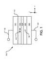
In one implementation, a read element according to the presently disclosed technology allows for soft magnetic side shielding, which results in a narrower track width of the read element than a corresponding read element with hard magnetic side shielding. The soft magnetic side shielding may be narrower because junction/permanent magnetic interactions are eliminated. Further, the presently disclosed read element provides a detection resolution increase and reduction of noise interference. These advantages mitigate an incremental shield-to-shield spacing increase caused by the additional top AFM layer as compared to a conventional read element.
FIG. 1 illustrates an examplemagnetic structure100 with free layer stabilization. First and secondelectrical leads158,160 electrically connect themagnetic structure100 to a power source (not shown) and conduct a sense current through themagnetic structure100 perpendicular to the major planes of the layers of themagnetic structure100. In one implementation, themagnetic structure100 is implemented as a magnetic memory cell.
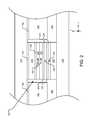
Themagnetic structure100 includes afree layer134 and a pinnedlayer138 with a nonmagnetic electrically conductive ornonconductive spacer layer144 there between. Polarity of thepinned layer138 is pinned by abottom AFM layer130. Thebottom AFM layer130 sets the polarity of the pinned layer138 (shown schematically by symbol146) approximately perpendicular to the depictedmagnetic structure100 in a direction toward the depictedmagnetic structure100 and parallel to the major planes of the various magnetic structure100 (e.g., in the negative z-direction).
Atop AFM layer132 biases the polarity of the free layer134 (shown schematically by symbols150) approximately parallel to the depictedmagnetic structure100 and approximately parallel to the major planes of the variousmagnetic structure100 layers (e.g., in the x-direction). In some implementations, it is difficult to align the polarity bias of thefree layers134 exactly parallel to the depictedmagnetic structure100 and major planes of the variousmagnetic structure100 layers. In one embodiment, the polarity bias of thefree layers134 is within 15 degrees of parallel to the depictedmagnetic structure100 and 15 degrees of parallel to the major planes of the variousmagnetic structure100 layers. A greater range may still allow themagnetic structure100 to function sufficiently, as well.
When the magnetic polarity of thefree layer134 is rotated into the negative z-direction, thesymbols146 and150 become more anti-parallel which illustrates an increase in the resistance of themagnetic structure100 to a sense current passing between the first and secondelectrical leads158,160. Conversely, when the magnetic polarity of thefree layer134 is rotated in the positive z-direction, thesymbols146 and150 become more parallel, which illustrates a decrease in the resistance of themagnetic structure100 to the sense current passing between the first and secondelectrical leads158,160.
Atuning layer152 is positioned between thetop AFM layer132 and thefree layer134. The thickness of thetuning layer152 is tuned or optimized to provide a desired bias level (i.e., magnetic coupling) to thefree layer134. In other words, the bias level of thefree layer134 is tuned to a desired level by selecting a material and/or thickness of thetuning layer152. For example, a particularlythin tuning layer152 will place thetop AFM layer132 and thefree layer134 close together, thus the polarity bias from thetop AFM layer132 on thefree layer134 will be particularly strong (or stiff). Conversely, a particularlythick tuning layer152 will place thetop AFM layer132 and thefree layer134 not as close together, thus the polarity bias from thetop AFM layer132 on thefree layer134 will not be as strong (or more flexible). Strength of the bias level is selected to obtain a desired sensitivity of themagnetic structure100 while allowing themagnetic structure100 to remain sufficiently stable. In other words, theturning layer152 decouples thefree layer134 from thetop AFM layer132 and reduces dispersion of the free layer magnetic moment.
As compared to an implementation without a spacer layer, incorporation of thetuning layer152 in themagnetic structure100 allows a high pinning field strength of thetop AFM layer132 to be maintained while reducing dispersion of the pinning field. Further, thetuning layer152 reduces coercivity of the pinning field of thetop AFM layer132. Low coercivity is desirable to reduce effects of external thermal and/or magnetic signals on the polarity of thetop AFM layer132. Different materials and thicknesses of thetuning layer152 affect pinning field strength, dispersion of the pinning field, and coercivity of thetuning layer152.
FIG. 2 illustrates an air bearing surface of an example readelement200 withdual AFM layers230,232 and softmagnetic side shields222. Theread element200 is shown as viewed from a magnetic media looking upwards at the air bearing surface (ABS) of theread element200. Theread element200 is located between first andsecond shields216,218 that also serve as first and second electrical lead layers. The first andsecond shields216,218 conduct a sense current through theread element200 perpendicular to the major planes of the layers of theread element200. Theread element200, in this implementation, includes first and secondfree layers234,236 laminated together. In other implementations, there is only one free layer or more than two free layers laminated together.
Theread element200 also includes a pinned layer lamination including first and second pinnedlayers238,240 and aninterlayer242 between thepinned layers238,240. Theinterlayer242 is a nonmagnetic electrically conductive anti-parallel coupling (APC) that interfaces the two pinnedlayers238,240 together. In some implementations, layers238,240,242 together form a synthetic anti-ferromagnet (SAF). A nonmagnetic electrically conductive or nonconductive spacer orbarrier layer244 is located between thefree layer lamination234,236 and the pinned layer lamination.
Polarity of the pinnedlayers238,240 is pinned by abottom AFM layer230. Thebottom AFM layer230 sets the polarity of pinned layer238 (shown schematically by symbol246) approximately perpendicular to the depicted ABS plane in a direction toward the depicted ABS and parallel to the major planes of thevarious read element200 layers (e.g., in the negative z-direction). Polarity of AFM layer232 (shown schematically by symbol248) is oriented anti-parallel (e.g., in the z-direction) topolarity246 by a strong anti-parallel coupling between the pinnedlayers238,240 provided by theinterlayer242. In another implementation, polarity of the pinnedlayer238 is oriented away from the depicted ABS and polarity of theAFM layer232 is oriented toward the depicted ABS. In yet another implementation, the polarities of pinnedlayers238,240 are parallel to the depicted ABS plane.
Thetop AFM layer232 biases the polarity of the laminatedfree layers234,236 (shown schematically by symbols250) approximately parallel to the depicted ABS and approximately parallel to the major planes of thevarious read element200 layers (e.g., in the x-direction). In some implementations, it is difficult to align the polarity bias of the laminatedfree layers234,236 exactly parallel to the depicted ABS and major planes of thevarious read element200 layers. In one embodiment, the polarity bias of the laminatedfree layers234,236 is within 15 degrees of parallel to the depicted ABS and 15 degrees of parallel to the major planes of thevarious read element200 layers. A greater range may still allow theread element200 to function sufficiently, as well.
When a field signal from a magnetic media rotates the magnetic polarity of the laminatedfree layers234,236 into the depicted ABS (e.g., in the negative z-direction), thesymbols248 and250 become more anti-parallel which illustrates an increase in the resistance of the readelement200 to a sense current passing between the first andsecond shields216,218. Conversely, when a field signal from the magnetic media rotates the magnetic polarity of the laminatedfree layers234,235 out of the depicted ABS (e.g., in the z-direction), thesymbols248 and250 become more parallel, which illustrates a decrease in the resistance of the readelement200 to the sense current passing between the first andsecond shields216,218.
Tuning layer252 is positioned between thetop AFM layer232 and thefree layers234,236. The thickness of thetuning layer252 is tuned or optimized to provide a desired bias level (i.e., magnetic coupling) to thefree layers234,236. In other words, the bias level of thefree layers234,236 is tuned to a desired level by selecting a material and/or thickness of thetuning layer252. For example, a particularlythin tuning layer252 will place thetop AFM layer232 andfree layers234,236 close together, thus the polarity bias from thetop AFM layer232 on thefree layers234,236 will be particularly strong (or stiff). Conversely, a particularlythick tuning layer252 will place thetop AFM layer232 andfree layers234,236 not as close together, thus the polarity bias from thetop AFM layer232 on thefree layers234,236 will not be as strong (or more flexible). Strength of the bias level is selected to obtain a desired sensitivity of the readelement200 while allowing theread element200 to remain sufficiently stable.
AnAFM cap254 is placed on theAFM layer232 to protect theAFM layer232 from corrosion and subsequent processing steps. In some implementations, an additional seed layer is placed between theAFM layer232 andsecond shield218 that prepares the readelement200 for application of thesecond shield218. For example, the seed layer is adapted to accept a plating operation that places thesecond shield218 on theread element200.
As compared to an implementation without a spacer layer, incorporation of thetuning layer252 in theread element200 allows a high pinning field strength of thetop AFM layer232 to be maintained while reducing dispersion of the pinning field. Further, thetuning layer252 reduces coercivity of the pinning field of thetop AFM layer232. Low coercivity is desirable to reduce effects of external thermal and/or magnetic signals on the polarity of thetop AFM layer232. Different materials and thicknesses of thetuning layer252 affect pinning field strength, dispersion of the pinning field, and coercivity of thetuning layer252. In some implementations thetuning layer252 is sandwiched between two layers of an AFM layer rather than adjacenttop AFM layer232 as shown inFIG. 2. In other implementations, there are multiple spacer layers (soft magnetic and/or nonmagnetic) to maximize pinning field strength while minimizing dispersion of the pinning field. Thetuning layer252 may decrease dispersion of the pinning field by as much as 50% without causing major degradation of the pinning field.
Sides of the readelement200 are surrounded by a non-magnetic, non-conductive filler material220 (e.g., alumina). Further, soft magnetic side shields222 are used on the sides of the readelement200 to reduce electromagnetic interference (e.g., side reading consideration and stray field noise), primarily x-direction interference and/or z-direction interference. The soft magnetic side shields222 are separated from thetop shield218 by side shield caps256 andbottom shield216 by thefiller material220. Use of soft magnetic side shields222 (as opposed to hard magnetic side shields) allows for sub-100 nm thickness of the readelement200 andshields216,218 collectively, as discussed above. In one implementation, the side shields222 are NiFe. In other implementations, the side shields222 are non-magnetic. In still other implementations, the side shields222,top shield218, andbottom shield216 are made of the same soft magnetic material. In yet other implementations, theshields222,top shield218, andbottom shield216 are made of a non-magnetic material.
One implementation of the presently disclosed technology utilizes the following materials and thicknesses. Thebottom AFM layer230 may be made of IrMn and/or PtMn and have a thickness ranging from 30-250 Angstrom(Å). Each of the pinninglayers238,240 may also be made of high coercivity materials such as CoPt, CoPtCr, FePt, CoPtCrTa, and/or various materials derived from CoPt, CoPtCr, FePt, and/or CoPtCrTa and have a thickness ranging from 20-150 A. In other implementations, each of the pinninglayers238,240 may be made of low coercivity materials such as CoFe, CoNiFe, and/or CoFeB. Theinterlayer242 may be made of chromium, ruthenium, and/or rhodium and have a thickness ranging up to 10 A. In some implementations, there is nointerlayer242. Thespacer layer244 may be made of titanium oxide, alumina, magnesium oxide, and/or a conductive material (e.g., copper or a copper alloy) and have a thickness ranging up to 30 A.
The free layer(s)234,236 may be made of NiFe and/or CoFe and have thicknesses ranging from 20-50 A. Thetuning layer252 may be made of chromium, ruthenium, tantalum, and/or rhodium and have a thickness ranging up to 10 A. In some implementations, there is notuning layer252. Thetop AFM layer232 may be made of IrMn and/or PtMn and have a thickness ranging from 30-100 A. TheAFM cap254 may be made of chromium, ruthenium, and/or rhodium and have a thickness ranging up to 50 A. In some implementations, there is noAFM cap254. The soft magnetic side shields222 may be made of NiFe alloys and have a thickness ranging from 50-200 A. The side shield caps256 may be made of chromium, ruthenium, and/or rhodium and have a thickness ranging up to 100 A. In some implementations, there are no side shield caps256. Each of the first andsecond shields216,218 may be made of NiFe alloys and have a thickness ranging from 1-2 microns.
In various implementations, the presently disclosed technology is applicable to high density perpendicular media, discrete track recording (DTR), and/or bit patterned media (BPM). Further, the presently disclosed technology is capable of thermal reliability up to at least 200°-250° C.
FIG. 3 illustratesexample operations300 for manufacturing a read element according to the presently disclosed technology. In adeposition operation310, a bottom shield, seed AFM layer, first pinned layer, interlayer, second pinned layer, spacer layer, and free layer(s) are sequentially deposited on a semiconductor wafer (e.g., an AlTiC wafer) using conventional transducer processing techniques. In asecond deposition operation315, a tuning layer is deposited on the free layer(s) of the read element. In many implementations, thesecond deposition operation315 is performed at a temperature ranging between 20° C. and 400° C.
In athird deposition operation320, a second AFM layer and an AFM capping layer are sequentially deposited on the tuning layer. Substrate temperature during deposition and thickness of the second AFM layer control bias in the free layer(s). In one implementation, the objective for the second AFM pinning of the free layers is to establish a free layer bias in the order of 250-800 Oe in a direction perpendicular to the first AFM pinning direction. Further, thickness of the tuning layer also affects the pinning in the free layers. The thicknesses of the free layer(s) and AFM layers, and substrate temperatures during deposition are also optimized to maintain thermal stability, repeatability, and bias on the read element.
In a readelement definition operation325, photolithography and ion beam etch processing set the reader geometry for a desired read track width. Further, an alumina material is deposited over exposed sides of the aforementioned layers. The alumina material electrically isolates the aforementioned layers from electrical transmission in a direction coplanar to the aforementioned layers (e.g., to adjacent soft magnetic material deposited in a fourth deposition operation330). As a result, the alumina material facilitates electrical conduction between the top and bottom shields, allowing for efficient read element operation.
In thefourth deposition operation330, a soft magnetic material is deposited adjacent to the alumina material. The soft magnetic material serves to magnetically shield the free layer(s) from external magnetic interference. In one implementation, soft magnetic material is coplanar to at least the free layer(s), tuning layer, and second AFM layer. The soft magnetic material may also be coplanar with one or more of the seed AFM layer, first pinned layer, interlayer, second pinned layer, spacer layer, and AFM capping layer. In some implementations, an additional capping layer is applied over the soft magnetic material. The capping layer(s) have adequate thickness to maintain the top exchange bias integrity through the definition process, post deposition.
In afifth deposition operation335, a seed layer and top shield are deposited on the AFM capping layer. In anannealing operation340, the AFM layers are annealed to set the magnetic orientation of the AFM layers. In many implementations, the magnetic orientation of the second AFM layer is set perpendicular to the magnetic orientation of the first AFM layer in a direction co-planar to on or more of the aforementioned layers. In some implementation, theannealing operation340 is performed between 1-5 kGauss at a temperature ranging from 215-235 degrees Celsius. In operation, electricity is conducted between the bottom shield and the top shield. Polarity of the free layer(s) changes with proximity to magnetic bits. As the polarity of the free layer(s) changes, overall resistance of the aforementioned layered structure changes. Changes in the resistance of current flowing in a direction perpendicular to the aforementioned layers affects a voltage differential between the bottom shield and the top shield. As a result, changes in the voltage differential are used to detect the presence and/or orientation of magnetic bits. Upon completion of the aforementioned stack deposition, photolithography and etch processes may follow without changes to customary processing of the transducer.
FIG. 4 illustratesexample operations400 for biasing a magnetic layered structure according to the presently disclosed technology. A definingoperation410 defines a magnetic orientation of a pinned layer using a first anti-ferromagnetic layer in the magnetic layered structure. A biasingoperation415 biases a magnetic orientation of a free layer in a direction perpendicular to the magnetic orientation of the pinned layer defined inoperation410 using a second anti-ferromagnetic layer in the magnetic layered structure.
Atuning operation420 tunes the free layer magnetic orientation to a desired level using a tuning layer. Thetuning operation420 balances reduction of noise interference with detection resolution within the magnetic layered structure. At least the material composition and thickness of the tuning layer affects the amount of tuning inoperation420. Anoptional decoupling operation425 decouples the free layer and the second anti-ferromagnetic layer from one another. In one implementation, a spacer layer positioned between the free layer and the second anti-ferromagnetic layer provides the decoupling of theoperation425. Anoptional shielding operation430 shields the free layer from external interference. In one implementation, one or more side shields placed adjacent the free layer along a major plane of the free layer provides the shielding ofoperation430.
FIG. 5 illustrates an air bearing surface of anexample read element500 with threeAFM layers530,532, and558. Theread element500 is shown as viewed from a magnetic media looking upwards at the air bearing surface (ABS) of the readelement500. The read element is located between first andsecond shields516 and518. Theread element500 includes first and secondfree layers534 and536 laminated together. Theread element500 also includes a pinned layer lamination including first and second pinnedlayers538,540, and aninterlayer542 between the pinnedlayers538,540. A nonmagnetic electrically conductive or nonconductive spacer orbarrier layer544 is located between thefree layer lamination534,536, and the pinned layer lamination.
Polarity of the pinnedlayers538,540 is pinned by abottom AFM layer530. Thetop AFM layer552 and amiddle AFM layer558 biases the polarity of the laminatedfree layers534,536. The polarity of the pinnedlayers538,540,free layers534,536, and top and bottom AFM layers530 and552 may be the same or similar to such layers illustrated and described with respect toFIG. 2.
Atuning element552 is sandwiched between thetop AFM layer532 and themiddle AFM layer558. The thickness of thetuning layer552 may be tuned or optimized to provide a desired bias level (i.e., magnetic coupling) to thefree layers534,536. Such tuning may be performed in a same or a similar manner to that described above with respect toFIG. 2.
Sides of the readelement500 are surrounded by a non-magnetic, non-conductive filler material520 (e.g., alumina). Soft magnetic side shields522 are used on the side of the readelement500. The soft magnetic side shields522 are separated from thetop shield518 by side shield caps556 andbottom shield516 by thefiller material520.
The above specification, examples, and data provide a complete description of the structure and use of exemplary embodiments of the invention. Since many embodiments of the invention can be made without departing from the spirit and scope of the invention, the invention resides in the claims hereinafter appended. Furthermore, structural features of the different embodiments may be combined in yet another embodiment without departing from the recited claims.

Claims (21)

What is claimed is:
1. A magnetic layered structure comprising:
a pinned layer;
a first anti-ferromagnetic layer that defines a magnetic orientation of the pinned layer;
a free layer;
a second anti-ferromagnetic layer and a third anti-ferromagnetic layer that bias the free layer to a magnetic orientation approximately perpendicular to the magnetic orientation of the pinned layer; and
a tuning layer that tunes free layer bias to a desired level and is separated from the free layer and positioned between the second anti-ferromagnetic layer and the third anti-ferromagnetic layer.
2. The magnetic layered structure ofclaim 1, further comprising:
one or more side shields positioned adjacent the free layer along a major plane of the free layer.
3. The magnetic layered structure ofclaim 2, wherein the side shields include a soft magnetic material.
4. The magnetic layered structure ofclaim 2, wherein the side shields include a non-magnetic material.
5. The magnetic layered structure ofclaim 1, further comprising:
two electrodes, each positioned on opposite sides of the layered structure, configured to conduct current through the layered structure along an axis approximately perpendicular to a major plane of the free layer.
6. The magnetic layered structure ofclaim 1, further comprising:
a spacer layer that magnetically separates the pinned layer from the free layer.
7. The magnetic layered structure ofclaim 1, further comprising:
a capping layer that protects the second anti-ferromagnetic layer from post deposition damage.
8. The magnetic layered structure ofclaim 1, wherein the pinned layer, first anti-ferromagnetic layer, free layer, and second anti-ferromagnetic layer comprise a read element sensor.
9. The magnetic layered structure ofclaim 1, wherein approximately perpendicular is perpendicular +/−15 degrees.
10. The magnetic layered structure ofclaim 1, wherein the first and second anti-ferromagnetic layers comprise IrMn or PtMn and have a thickness greater than or equal to 30 Å and less than or equal to 250 Å.
11. The magnetic layered structure ofclaim 1, wherein the free layer comprises a first free layer and a second free layer.
12. The magnetic layered structure ofclaim 1, wherein the structure further comprises multiple spacer layers including at least one of soft magnetic or nonmagnetic material to increase pinning field strength.
13. The magnetic layered structure ofclaim 1, wherein the tuning layer decouples the free layer and the second anti-ferromagnetic layer while reducing dispersion of a free layer magnetic moment.
14. A method of biasing a magnetic layered structure, comprising:
defining a magnetic orientation of a pinned layer using a first anti-ferromagnetic layer;
biasing a magnetic orientation of a free layer using a second anti-ferromagnetic layer and a third anti-ferromagnetic layer, wherein the defined magnetic orientation of the pinned layer is approximately perpendicular to the biased magnetic orientation of the free layer; and
tuning free layer bias to a desired level using a tuning layer that decouples the free layer and the second anti-ferromagnetic layer wherein the tuning layer is separated from the free layer and positioned between the second anti-ferromagnetic layer and the third anti-ferromagnetic layer.
15. The method ofclaim 14, further comprising:
shielding the free layer from external electromagnetic and/or thermal interference using one or more side shields positioned adjacent the free layer along a major plane of the free layer.
16. The method ofclaim 14, further comprising:
conducting current along an axis approximately perpendicular to a major plane of the free layer between two electrodes positioned on opposite sides of the first anti-ferromagnetic layer, pinned layer, free layer, and second anti-ferromagnetic layer.
17. The method ofclaim 14, further comprising:
decoupling the free layer and the second anti-ferromagnetic layer while reducing dispersion of a free layer magnetic moment.
18. The method ofclaim 14, further comprising:
decoupling the free layer and the second anti-ferromagnetic layer while reducing dispersion of a free layer magnetic moment.
19. A transducer for a magnetic disc drive comprising:
a reader, including
a pinned layer;
a first anti-ferromagnetic layer that defines a magnetic orientation of the pinned layer;
a free layer;
a second anti-ferromagnetic layer and a third anti-ferromagnetic layer that bias the free layer to a magnetic orientation approximately perpendicular to the magnetic orientation of the pinned layer; and
a tuning layer that tunes free layer bias to a desired level, wherein the tuning layer is separated from the free layer and positioned between the second anti-ferromagnetic layer and the third antiferromagnetic layer.
20. The transducer ofclaim 19, wherein the reader further includes one or more side shields positioned adjacent the free layer along a major plane of the free layer that shields the free layer from external electromagnetic interference.
21. The transducer ofclaim 19, wherein the reader further includes two electrodes, each positioned on opposite sides of the layered structure, configured to conduct current through the layered structure along an axis approximately perpendicular to a major plane of the free layer.
US12/972,1822010-12-172010-12-17Magnetic structure free layer stabilizationActive2031-10-31US8531802B2 (en)

Priority Applications (3)

Application NumberPriority DateFiling DateTitle
US12/972,182US8531802B2 (en)2010-12-172010-12-17Magnetic structure free layer stabilization
JP2011268940AJP2012134481A (en)2010-12-172011-12-08Magnetic layer structure, method of biasing magnetic layer structure, and converter
US13/961,116US20130321954A1 (en)2010-12-172013-08-07Magnetic structure free layer stabilization

Applications Claiming Priority (1)

Application NumberPriority DateFiling DateTitle
US12/972,182US8531802B2 (en)2010-12-172010-12-17Magnetic structure free layer stabilization

Related Child Applications (1)

Application NumberTitlePriority DateFiling Date
US13/961,116ContinuationUS20130321954A1 (en)2010-12-172013-08-07Magnetic structure free layer stabilization

Publications (2)

Publication NumberPublication Date
US20120154955A1 US20120154955A1 (en)2012-06-21
US8531802B2true US8531802B2 (en)2013-09-10

Family

ID=46234089

Family Applications (2)

Application NumberTitlePriority DateFiling Date
US12/972,182Active2031-10-31US8531802B2 (en)2010-12-172010-12-17Magnetic structure free layer stabilization
US13/961,116AbandonedUS20130321954A1 (en)2010-12-172013-08-07Magnetic structure free layer stabilization

Family Applications After (1)

Application NumberTitlePriority DateFiling Date
US13/961,116AbandonedUS20130321954A1 (en)2010-12-172013-08-07Magnetic structure free layer stabilization

Country Status (2)

CountryLink
US (2)US8531802B2 (en)
JP (1)JP2012134481A (en)

Cited By (2)

* Cited by examiner, † Cited by third party
Publication numberPriority datePublication dateAssigneeTitle
US10068601B1 (en)*2016-08-092018-09-04Western Digital (Fremont), LlcFree layer only magnetic reader that may have a reduced shield-to-shield spacing and a multilayer side bias
US10204671B2 (en)2017-03-102019-02-12Simon Fraser UniversityApplications of non-collinearly coupled magnetic layers

Families Citing this family (5)

* Cited by examiner, † Cited by third party
Publication numberPriority datePublication dateAssigneeTitle
US8829901B2 (en)*2011-11-042014-09-09Honeywell International Inc.Method of using a magnetoresistive sensor in second harmonic detection mode for sensing weak magnetic fields
US8576518B1 (en)2012-10-302013-11-05HGST Netherlands B.V.Current-perpendicular-to-the-plane (CPP) magnetoresistive (MR) sensor with exchange-coupled side shield structure
US8780506B1 (en)2013-06-202014-07-15HGST Netherlands B.V.Current-perpendicular-to-the-plane (CPP) magnetoresistive (MR) sensor with side shields and an antiparallel structure top shield
JP6282990B2 (en)*2015-02-242018-02-21アルプス電気株式会社 Magnetic sensor and current sensor
US11821818B2 (en)2017-07-062023-11-21University Of Houston SystemBiosensor for detecting a single magnetic label

Citations (18)

* Cited by examiner, † Cited by third party
Publication numberPriority datePublication dateAssigneeTitle
US5923505A (en)1997-03-171999-07-13Read-Rite CorporationMagnetoresistive sensor having a pinned soft magnetic layer
US6292335B1 (en)1999-06-252001-09-18International Business Machines CorporationContinuous junction spin valve read head stabilized without hard bias layers
US20020034056A1 (en)*2000-09-192002-03-21Lujun ChenGiant magnetoresistive sensor having selfconsistent demagnetization fields
US6473279B2 (en)2001-01-042002-10-29International Business Machines CorporationIn-stack single-domain stabilization of free layers for CIP and CPP spin-valve or tunnel-valve read heads
US6563682B1 (en)*1999-08-302003-05-13Sony CorporationMagneto resistive element
US6671139B2 (en)2002-01-312003-12-30International Business Machines CorporationIn-stack longitudinal bias structure for CIP spin valve sensors with bias layer electrically insulated from free layer
US6704175B2 (en)*2001-03-282004-03-09Tdk CorporationCurrent perpendicular-to-the-plane magnetoresistance read head
US6741432B2 (en)2002-03-212004-05-25International Business Machines CorporationCurrent perpendicular to the planes (CPP) spin valve sensor with in-stack biased free layer and self-pinned antiparallel (AP) pinned layer structure
US6831816B2 (en)2002-07-152004-12-14International Business Machines CorporationCPP sensor with in-stack biased free layer
US20060103991A1 (en)*2004-11-152006-05-18Hitachi Global Storage TechnologiesMagnetoresistive head using longitudinal biasing method with 90-degree magnetic interlayer coupling and manufacturing method thereof
US20060176621A1 (en)*2005-02-072006-08-10Hitachi Global Storage TechnologiesMagnetoresistive sensor with free layer bias adjustment capability
US20060187591A1 (en)*2005-02-232006-08-24Hitachi Global Storage TechnologiesMagnetoresistive sensor with a free layer stabilized by direct coupling to in stack antiferromagnetic layer
US20070195469A1 (en)*2006-02-172007-08-23Kabushiki Kaisha ToshibaMagnetoresistive effect element, magnetic head, magnetic reproducing apparatus, and manufacturing method of magnetoresistive effect element
US20070211393A1 (en)*2006-03-082007-09-13Gill Hardayal SMethod and apparatus for using a specular scattering layer in a free layer of a magnetic sensor while stabilizing the free layer by direct coupling with an antiferromagnetic layer
US7446986B2 (en)*2004-08-312008-11-04Hitachi Global Storage Technologies Netherlands B.V.Magnetic tunnel junction with in stack biasing layer providing orthogonal exchange coupling
US20090185315A1 (en)*2008-01-222009-07-23Seagate Technology LlcMagnetic sensor including a free layer having perpendicular to the plane anisotropy
US7602591B2 (en)*2005-06-222009-10-13Tdk CorporationExchange-coupled free layer with out-of-plane magnetization
US7663848B1 (en)*2006-07-142010-02-16Grandis, Inc.Magnetic memories utilizing a magnetic element having an engineered free layer

Family Cites Families (9)

* Cited by examiner, † Cited by third party
Publication numberPriority datePublication dateAssigneeTitle
JP2002232039A (en)*2001-02-022002-08-16Sony CorpSpin valve type huge magnetoresistance effect element, magnetoresistance effect type magnetic head and their manufacturing methods
JP2002304709A (en)*2001-04-092002-10-18Sony CorpMagnetic head and its manufacturing device
JP2002359415A (en)*2001-05-312002-12-13Sony CorpVertical-to-surface current type magnetoresistive effect element, manufacturing method therefor, reproducing head, information storage device mounting the same
JP2003298147A (en)*2002-04-022003-10-17Tdk CorpMagneto-resistance effect element, magnetic head, head suspension assembly and magnetic disk device
US7525775B2 (en)*2005-11-172009-04-28Hitachi Global Storage Technologies Netherlands B.V.Oblique angle etched underlayers for improved exchange biased structures in a magnetoresitive sensor
JP2007287239A (en)*2006-04-172007-11-01Hitachi Global Storage Technologies Netherlands Bv Magnetic head and method for forming the same
US7932571B2 (en)*2007-10-112011-04-26Everspin Technologies, Inc.Magnetic element having reduced current density
JP5383145B2 (en)*2008-10-152014-01-08エイチジーエスティーネザーランドビーブイ Magnetic read head
US8023230B2 (en)*2008-10-272011-09-20Tdk CorporationMagnetoresistive element including a pair of ferromagnetic layers coupled to a pair of shield layers

Patent Citations (18)

* Cited by examiner, † Cited by third party
Publication numberPriority datePublication dateAssigneeTitle
US5923505A (en)1997-03-171999-07-13Read-Rite CorporationMagnetoresistive sensor having a pinned soft magnetic layer
US6292335B1 (en)1999-06-252001-09-18International Business Machines CorporationContinuous junction spin valve read head stabilized without hard bias layers
US6563682B1 (en)*1999-08-302003-05-13Sony CorporationMagneto resistive element
US20020034056A1 (en)*2000-09-192002-03-21Lujun ChenGiant magnetoresistive sensor having selfconsistent demagnetization fields
US6473279B2 (en)2001-01-042002-10-29International Business Machines CorporationIn-stack single-domain stabilization of free layers for CIP and CPP spin-valve or tunnel-valve read heads
US6704175B2 (en)*2001-03-282004-03-09Tdk CorporationCurrent perpendicular-to-the-plane magnetoresistance read head
US6671139B2 (en)2002-01-312003-12-30International Business Machines CorporationIn-stack longitudinal bias structure for CIP spin valve sensors with bias layer electrically insulated from free layer
US6741432B2 (en)2002-03-212004-05-25International Business Machines CorporationCurrent perpendicular to the planes (CPP) spin valve sensor with in-stack biased free layer and self-pinned antiparallel (AP) pinned layer structure
US6831816B2 (en)2002-07-152004-12-14International Business Machines CorporationCPP sensor with in-stack biased free layer
US7446986B2 (en)*2004-08-312008-11-04Hitachi Global Storage Technologies Netherlands B.V.Magnetic tunnel junction with in stack biasing layer providing orthogonal exchange coupling
US20060103991A1 (en)*2004-11-152006-05-18Hitachi Global Storage TechnologiesMagnetoresistive head using longitudinal biasing method with 90-degree magnetic interlayer coupling and manufacturing method thereof
US20060176621A1 (en)*2005-02-072006-08-10Hitachi Global Storage TechnologiesMagnetoresistive sensor with free layer bias adjustment capability
US20060187591A1 (en)*2005-02-232006-08-24Hitachi Global Storage TechnologiesMagnetoresistive sensor with a free layer stabilized by direct coupling to in stack antiferromagnetic layer
US7602591B2 (en)*2005-06-222009-10-13Tdk CorporationExchange-coupled free layer with out-of-plane magnetization
US20070195469A1 (en)*2006-02-172007-08-23Kabushiki Kaisha ToshibaMagnetoresistive effect element, magnetic head, magnetic reproducing apparatus, and manufacturing method of magnetoresistive effect element
US20070211393A1 (en)*2006-03-082007-09-13Gill Hardayal SMethod and apparatus for using a specular scattering layer in a free layer of a magnetic sensor while stabilizing the free layer by direct coupling with an antiferromagnetic layer
US7663848B1 (en)*2006-07-142010-02-16Grandis, Inc.Magnetic memories utilizing a magnetic element having an engineered free layer
US20090185315A1 (en)*2008-01-222009-07-23Seagate Technology LlcMagnetic sensor including a free layer having perpendicular to the plane anisotropy

Non-Patent Citations (6)

* Cited by examiner, † Cited by third party
Title
Barker et al., "A model of the exchange bias setting process in magnetic read sensors" Jul. 13, 2009, Applied Physics Letters 95, 022504 (2009), 2009 American Institute of Physics, 3 pages.
Deac et al., "Current-induced magnetization switching in exchange-biased spin valves for current-perpendicular-to-plane giant magnetoresistance heads" Feb. 9, 2006, Physical Review B 73, 064414 (2006) The American Physical Society, 8 pages.
Hung et al., "Exchange biasing and thermal stability of CoFe/PtPdMn films" Exchange Biasing I: Experiment and Theory, May 1, 2000, Journal of Applied Physics, vol. 87, No. 9, 3 pages.
Kanai et al., "Advanced Spin-Valve GMR Head" UDC 681.327.634, Fujitsu Sci. Tech. J., 37, 2,p. 174-182 (Dec. 2001).
Sanders et al., "Stabilization Films for Dual Stripe Read Sensors" Sep. 5, 2000, IEEE Transactions on Magnetics, vol. 36, No. 5, 3 pages.
T.C. Schulthess and W.H. Butler, "Coupling mechanisms in exchange biased films" Exchange Bias II, Apr. 15, 1999, Journal of Applied Physics, vol. 85, No. 8, 6 pages.

Cited By (3)

* Cited by examiner, † Cited by third party
Publication numberPriority datePublication dateAssigneeTitle
US10068601B1 (en)*2016-08-092018-09-04Western Digital (Fremont), LlcFree layer only magnetic reader that may have a reduced shield-to-shield spacing and a multilayer side bias
US10204671B2 (en)2017-03-102019-02-12Simon Fraser UniversityApplications of non-collinearly coupled magnetic layers
US10446208B2 (en)2017-03-102019-10-15Simon Fraser UniversityApplications of non-collinearly coupled magnetic layers

Also Published As

Publication numberPublication date
JP2012134481A (en)2012-07-12
US20130321954A1 (en)2013-12-05
US20120154955A1 (en)2012-06-21

Similar Documents

PublicationPublication DateTitle
US8873204B1 (en)Current-perpendicular-to-the-plane (CPP) magnetoresistive (MR) sensor structure with multiple stacked sensors and center shield with CoFeB insertion layer
US9042059B1 (en)Current-perpendicular-to-the-plane (CPP) magnetoresistive (MR) sensor structure with multiple stacked sensors and improved center shield
US7035058B2 (en)Magneto-resistive effect element, magnetic sensor using magneto-resistive effect, magnetic head using magneto-resistive effect and magnetic memory
US6600638B2 (en)Corrosion resistive GMR and MTJ sensors
US8437105B2 (en)Magnetic sensor with composite magnetic shield
US6828785B2 (en)Magneto-resistive effect element, magnetic sensor using magneto-resistive effect, magnetic head using magneto-resistive effect and magnetic memory
US20130321954A1 (en)Magnetic structure free layer stabilization
US20110007426A1 (en)Trapezoidal back bias and trilayer reader geometry to enhance device performance
US20100232072A1 (en)Magnetic sensor with a recessed reference layer assembly and a front shield
US9001473B1 (en)TMR/CPP reader for narrow reader gap application
JP2009099741A (en) Ferromagnetic tunnel junction device, method for manufacturing ferromagnetic tunnel junction device, magnetic head, magnetic storage device, and magnetic memory device
US8891208B2 (en)CPP-type magnetoresistive element including a rear bias structure and lower shields with inclined magnetizations
US9183858B2 (en)Dual capping layer utilized in a magnetoresistive effect sensor
CN102737649A (en)Current-perpendicular-to-the-plane (cpp) magnetoresistive (mr) sensor with improved hard magnet biasing structure
US8988833B2 (en)Current-perpendicular-to-the-plane (CPP) magnetoresistive sensor with reduced-width top and bottom electrodes and method for making
US7606008B2 (en)Stabilizer for magnetoresistive head and method of manufacture
US9129622B2 (en)CPP-type magnetoresistance effect element and magnetic disk device
US9401162B1 (en)Read sensor with free layers of different widths sandwiching a SAF structure for extremely high resolution
US6807033B2 (en)Magnetic sensor with reduced wing region magnetic sensitivity
WO2005101377A1 (en)Stabilizer for magnetoresistive head in current perpendicular to plane mode and method of manufacture
US20070091513A1 (en)Stabilized spin valve head and method of manufacture
US10249329B1 (en)Current-perpendicular-to-the-plane (CPP) magnetoresistive (MR) sensor with wedge shaped free layer
US20080239588A1 (en)Magneto-resistance effect element, magnetic head, and magnetic recording/reproducing device
US7573686B2 (en)Thin-film magnetic head including low-resistance TMR element
US20080218912A1 (en)CPP-type magnetoresistive element having spacer layer that includes semiconductor layer

Legal Events

DateCodeTitleDescription
ASAssignment

Owner name:SEAGATE TECHNOLOGY LLC, CALIFORNIA

Free format text:ASSIGNMENT OF ASSIGNORS INTEREST;ASSIGNORS:TSOUKATOS, ANTONIA;SINGLETON, ERIC WALTER;SIGNING DATES FROM 20101213 TO 20101217;REEL/FRAME:025524/0293

ASAssignment

Owner name:THE BANK OF NOVA SCOTIA, AS ADMINISTRATIVE AGENT, CANADA

Free format text:SECURITY AGREEMENT;ASSIGNOR:SEAGATE TECHNOLOGY LLC;REEL/FRAME:026010/0350

Effective date:20110118

Owner name:THE BANK OF NOVA SCOTIA, AS ADMINISTRATIVE AGENT,

Free format text:SECURITY AGREEMENT;ASSIGNOR:SEAGATE TECHNOLOGY LLC;REEL/FRAME:026010/0350

Effective date:20110118

STCFInformation on status: patent grant

Free format text:PATENTED CASE

FPAYFee payment

Year of fee payment:4

FEPPFee payment procedure

Free format text:MAINTENANCE FEE REMINDER MAILED (ORIGINAL EVENT CODE: REM.); ENTITY STATUS OF PATENT OWNER: LARGE ENTITY

FEPPFee payment procedure

Free format text:7.5 YR SURCHARGE - LATE PMT W/IN 6 MO, LARGE ENTITY (ORIGINAL EVENT CODE: M1555); ENTITY STATUS OF PATENT OWNER: LARGE ENTITY

MAFPMaintenance fee payment

Free format text:PAYMENT OF MAINTENANCE FEE, 8TH YEAR, LARGE ENTITY (ORIGINAL EVENT CODE: M1552); ENTITY STATUS OF PATENT OWNER: LARGE ENTITY

Year of fee payment:8

MAFPMaintenance fee payment

Free format text:PAYMENT OF MAINTENANCE FEE, 12TH YEAR, LARGE ENTITY (ORIGINAL EVENT CODE: M1553); ENTITY STATUS OF PATENT OWNER: LARGE ENTITY

Year of fee payment:12

ASAssignment

Owner name:SEAGATE TECHNOLOGY PUBLIC LIMITED COMPANY, CALIFORNIA

Free format text:RELEASE BY SECURED PARTY;ASSIGNOR:THE BANK OF NOVA SCOTIA;REEL/FRAME:072193/0001

Effective date:20250303

Owner name:SEAGATE TECHNOLOGY, CALIFORNIA

Free format text:RELEASE BY SECURED PARTY;ASSIGNOR:THE BANK OF NOVA SCOTIA;REEL/FRAME:072193/0001

Effective date:20250303

Owner name:SEAGATE TECHNOLOGY HDD HOLDINGS, CALIFORNIA

Free format text:RELEASE BY SECURED PARTY;ASSIGNOR:THE BANK OF NOVA SCOTIA;REEL/FRAME:072193/0001

Effective date:20250303

Owner name:I365 INC., CALIFORNIA

Free format text:RELEASE BY SECURED PARTY;ASSIGNOR:THE BANK OF NOVA SCOTIA;REEL/FRAME:072193/0001

Effective date:20250303

Owner name:SEAGATE TECHNOLOGY LLC, CALIFORNIA

Free format text:RELEASE BY SECURED PARTY;ASSIGNOR:THE BANK OF NOVA SCOTIA;REEL/FRAME:072193/0001

Effective date:20250303

Owner name:SEAGATE TECHNOLOGY INTERNATIONAL, CAYMAN ISLANDS

Free format text:RELEASE BY SECURED PARTY;ASSIGNOR:THE BANK OF NOVA SCOTIA;REEL/FRAME:072193/0001

Effective date:20250303

Owner name:SEAGATE HDD CAYMAN, CAYMAN ISLANDS

Free format text:RELEASE BY SECURED PARTY;ASSIGNOR:THE BANK OF NOVA SCOTIA;REEL/FRAME:072193/0001

Effective date:20250303

Owner name:SEAGATE TECHNOLOGY (US) HOLDINGS, INC., CALIFORNIA

Free format text:RELEASE BY SECURED PARTY;ASSIGNOR:THE BANK OF NOVA SCOTIA;REEL/FRAME:072193/0001

Effective date:20250303


[8]ページ先頭

©2009-2025 Movatter.jp