US8531801B1 - Method and system for providing a read transducer having a composite magnetic shield with smooth interfaces - Google Patents
Method and system for providing a read transducer having a composite magnetic shield with smooth interfacesDownload PDFInfo
- Publication number
- US8531801B1 US8531801B1US13/723,099US201213723099AUS8531801B1US 8531801 B1US8531801 B1US 8531801B1US 201213723099 AUS201213723099 AUS 201213723099AUS 8531801 B1US8531801 B1US 8531801B1
- Authority
- US
- United States
- Prior art keywords
- layer
- magnetic
- trilayer
- additional
- ferromagnetic
- Prior art date
- Legal status (The legal status is an assumption and is not a legal conclusion. Google has not performed a legal analysis and makes no representation as to the accuracy of the status listed.)
- Active
Links
- 230000005291magnetic effectEffects0.000titleclaimsabstractdescription228
- 238000000034methodMethods0.000titleclaimsabstractdescription21
- 239000002131composite materialSubstances0.000titledescription8
- 230000005294ferromagnetic effectEffects0.000claimsabstractdescription99
- 125000006850spacer groupChemical group0.000claimsabstractdescription59
- 229910052758niobiumInorganic materials0.000claimsdescription9
- 229910052715tantalumInorganic materials0.000claimsdescription9
- 229910052719titaniumInorganic materials0.000claimsdescription9
- 229910052721tungstenInorganic materials0.000claimsdescription9
- 229910052726zirconiumInorganic materials0.000claimsdescription9
- 239000010410layerSubstances0.000description331
- 230000008878couplingEffects0.000description17
- 238000010168coupling processMethods0.000description17
- 238000005859coupling reactionMethods0.000description17
- 229910001030Iron–nickel alloyInorganic materials0.000description15
- 230000005290antiferromagnetic effectEffects0.000description9
- 238000000151depositionMethods0.000description8
- 230000003746surface roughnessEffects0.000description8
- 229910052796boronInorganic materials0.000description4
- 239000000463materialSubstances0.000description4
- 230000007246mechanismEffects0.000description4
- 230000035699permeabilityEffects0.000description4
- 229910003321CoFeInorganic materials0.000description3
- 229910019236CoFeBInorganic materials0.000description3
- 230000002411adverseEffects0.000description3
- 239000000696magnetic materialSubstances0.000description3
- 230000005641tunnelingEffects0.000description3
- 230000004888barrier functionEffects0.000description2
- 229910000889permalloyInorganic materials0.000description2
- 239000002356single layerSubstances0.000description2
- 230000015572biosynthetic processEffects0.000description1
- 239000000470constituentSubstances0.000description1
- 230000008021depositionEffects0.000description1
- 239000003989dielectric materialSubstances0.000description1
- 230000003292diminished effectEffects0.000description1
- 230000005381magnetic domainEffects0.000description1
- 230000005415magnetizationEffects0.000description1
- 238000004519manufacturing processMethods0.000description1
- 238000007788rougheningMethods0.000description1
Images


Classifications
- G—PHYSICS
- G11—INFORMATION STORAGE
- G11B—INFORMATION STORAGE BASED ON RELATIVE MOVEMENT BETWEEN RECORD CARRIER AND TRANSDUCER
- G11B5/00—Recording by magnetisation or demagnetisation of a record carrier; Reproducing by magnetic means; Record carriers therefor
- G11B5/127—Structure or manufacture of heads, e.g. inductive
- G11B5/33—Structure or manufacture of flux-sensitive heads, i.e. for reproduction only; Combination of such heads with means for recording or erasing only
- G11B5/39—Structure or manufacture of flux-sensitive heads, i.e. for reproduction only; Combination of such heads with means for recording or erasing only using magneto-resistive devices or effects
- G11B5/3903—Structure or manufacture of flux-sensitive heads, i.e. for reproduction only; Combination of such heads with means for recording or erasing only using magneto-resistive devices or effects using magnetic thin film layers or their effects, the films being part of integrated structures
- G11B5/3906—Details related to the use of magnetic thin film layers or to their effects
- G11B5/3929—Disposition of magnetic thin films not used for directly coupling magnetic flux from the track to the MR film or for shielding
- G11B5/3932—Magnetic biasing films
- B—PERFORMING OPERATIONS; TRANSPORTING
- B82—NANOTECHNOLOGY
- B82Y—SPECIFIC USES OR APPLICATIONS OF NANOSTRUCTURES; MEASUREMENT OR ANALYSIS OF NANOSTRUCTURES; MANUFACTURE OR TREATMENT OF NANOSTRUCTURES
- B82Y10/00—Nanotechnology for information processing, storage or transmission, e.g. quantum computing or single electron logic
- G—PHYSICS
- G11—INFORMATION STORAGE
- G11B—INFORMATION STORAGE BASED ON RELATIVE MOVEMENT BETWEEN RECORD CARRIER AND TRANSDUCER
- G11B5/00—Recording by magnetisation or demagnetisation of a record carrier; Reproducing by magnetic means; Record carriers therefor
- G11B5/127—Structure or manufacture of heads, e.g. inductive
- G11B5/33—Structure or manufacture of flux-sensitive heads, i.e. for reproduction only; Combination of such heads with means for recording or erasing only
- G11B5/39—Structure or manufacture of flux-sensitive heads, i.e. for reproduction only; Combination of such heads with means for recording or erasing only using magneto-resistive devices or effects
- G11B5/3903—Structure or manufacture of flux-sensitive heads, i.e. for reproduction only; Combination of such heads with means for recording or erasing only using magneto-resistive devices or effects using magnetic thin film layers or their effects, the films being part of integrated structures
- G11B5/3906—Details related to the use of magnetic thin film layers or to their effects
- G11B5/3909—Arrangements using a magnetic tunnel junction
- G—PHYSICS
- G11—INFORMATION STORAGE
- G11B—INFORMATION STORAGE BASED ON RELATIVE MOVEMENT BETWEEN RECORD CARRIER AND TRANSDUCER
- G11B5/00—Recording by magnetisation or demagnetisation of a record carrier; Reproducing by magnetic means; Record carriers therefor
- G11B5/127—Structure or manufacture of heads, e.g. inductive
- G11B5/33—Structure or manufacture of flux-sensitive heads, i.e. for reproduction only; Combination of such heads with means for recording or erasing only
- G11B5/39—Structure or manufacture of flux-sensitive heads, i.e. for reproduction only; Combination of such heads with means for recording or erasing only using magneto-resistive devices or effects
- G11B2005/3996—Structure or manufacture of flux-sensitive heads, i.e. for reproduction only; Combination of such heads with means for recording or erasing only using magneto-resistive devices or effects large or giant magnetoresistive effects [GMR], e.g. as generated in spin-valve [SV] devices
Definitions
- FIG. 1depicts an air-bearing surface (ABS) view of a conventional read transducer 10 .
- the conventional read transducer 10includes shields 12 and 20 , sensor 14 and magnetic bias structures 16 .
- the read sensor 14is typically a giant magnetoresistive (GMR) sensor or tunneling magnetoresistive (TMR) sensor.
- the read sensor 14includes an antiferromagnetic (AFM) layer, a pinned layer, a nonmagnetic spacer layer, and a free layer. Also shown is a capping layer.
- seed layer(s)may be used.
- the free layerhas a magnetization sensitive to an external magnetic field. Thus, the free layer functions as a sensor layer for the magnetoresistive sensor 14 .
- the magnetic bias structures 16may be hard bias structures or soft bias structures 16 . These magnetic bias structures are used to magnetically bias the sensor layer of the sensor 14 .
- the magnetic moment of the shield 20may be unstable.
- there may be multiple magnetic domains within the shield 20Movement of domain walls and other changes to the magnetic moment of the shield 20 may introduce noise or otherwise adversely affect performance of the conventional read transducer 10 .
- a method and systemprovide a magnetic transducer having an air-bearing surface (ABS).
- the magnetic transducerincludes a first shield, a read sensor, magnetic bias structure(s) and a second shield.
- the read sensorincludes edge(s) which are adjacent to the magnetic bias structure(s).
- the read sensor and the magnetic bias structure(s)are between the first shield and the second shield.
- the second shieldincludes a first ferromagnetic layer, a nonmagnetic spacer layer, a second ferromagnetic layer and a pinning layer.
- the nonmagnetic spacer layeris between the first ferromagnetic layer and the second ferromagnetic layer.
- the first ferromagnetic layeris between the read sensor and the nonmagnetic spacer layer.
- the pinning layeris adjacent to the second ferromagnetic layer.
- the first ferromagnetic layeris coupled antiparallel with the second ferromagnetic layer.
- the first ferromagnetic layerincludes a plurality of magnetic layers interleaved with at least one trilayer. Each of the magnetic layers includes a plurality of crystalline grains.
- the trilayer(s)include an amorphous nonmagnetic layer. The amorphous nonmagnetic layer is less than three Angstroms thick such that the magnetic layers are ferromagnetically coupled.
- the trilayer(s)are configured such that the crystalline grains in one of the magnetic layers are decoupled from the crystalline grains in another of the magnetic layers.
- FIG. 1depicts a conventional read transducer.
- FIG. 2depicts an ABS view of a more recent magnetic recording read transducer.
- FIG. 3is an ABS view of an exemplary embodiment of a portion of a magnetic recording read transducer.
- FIG. 4depicts an ABS view of an exemplary embodiment of a portion of a shield in a magnetic recording read transducer.
- FIG. 5depicts an exemplary embodiment of a portion of trilayer structure used within a shield in a magnetic recording transducer.
- FIG. 6depicts another exemplary embodiment of a portion of trilayer structure used within a shield in a magnetic recording transducer.
- FIG. 7depicts another exemplary embodiment of a portion of trilayer structure used within a shield in a magnetic recording transducer.
- FIG. 8depicts another exemplary embodiment of a portion of a shield in a magnetic recording read transducer.
- FIG. 9depicts another exemplary embodiment of a portion of a shield in a magnetic recording read transducer.
- FIG. 10depicts another exemplary embodiment of a portion of a shield in a magnetic recording read transducer.
- FIG. 11is flow chart depicting an exemplary embodiment of a method for fabricating a magnetic recording read transducer.
- FIG. 2depicts an ABS view of a portion of a more recent magnetic read transducer 50 .
- the read transducer 50may be part of a read head or may be part of a merged head that also includes a write transducer.
- the transducer 50includes shields 52 and 60 , a read sensor 54 and soft magnetic bias structures 56 .
- the sensor 54 shownis a GMR or TMR sensor.
- the sensor 54includes a pinning layer, a pinned, a nonmagnetic spacer layer, a free layer, and a capping layer. For simplicity, these layers are not separately labeled in FIG. 2 .
- the sensor 54may also include seed layer(s) (not shown).
- the pinning layermay be omitted or may use a different pinning mechanism.
- the pinned layer and free layerare each shown as a single layer, but may include multiple layers including but not limited to a synthetic antiferromagnetic (SAF) structure.
- the nonmagnetic spacer layermay be a conductive layer, a tunneling barrier layer, or other analogous layer.
- GMR or TMR sensordepicted as a GMR or TMR sensor, in other embodiments, other structures and other sensing mechanisms may be used for the sensor.
- the magnetic bias structures 56may be soft bias structures fabricated with soft magnetic material(s).
- the soft magnetic bias structures 56have a high permeability and a coercivity of less than ten Oe. In some such embodiments, the soft magnetic bias structures 56 have a coercivity of not more than five Oe.
- the soft magnetic bias structures 56may include NiFe, such as Permalloy. Because the soft magnetic bias structures 56 have a magnetic moment, the soft magnetic bias structures 56 magnetically bias the free layer.
- the magnetic read transducer 50also includes an antiferromagnetically biased second shield 60 .
- the shield 60includes ferromagnetic layers 62 and 66 , nonmagnetic spacer layer 64 , and pinning layer 68 .
- the shield 60may also include a capping layer 70 .
- the ferromagnetic layers 62 and 66are separated by nonmagnetic spacer layer 64 .
- the ferromagnetic layers 62 and 66may include soft magnetic materials, such as NiFe.
- the nonmagnetic spacer layer 64may be Ru, which allows the magnetic moments of the layers 62 and 66 to be coupled antiparallel.
- the moment of the ferromagnetic layer 66is pinned by the pinning layer 68 .
- the pinning layeris typically an antiferromagnet (AFM), such as IrMn.
- the performance of the magnetic transducer 50may be improved. More specifically, the domains in the second shield 60 may be stabilized and noise reduced. However, as can be seen in FIG. 2 , the interfaces between the layers 62 , 64 , 66 and 68 are rather rough. Because of the surface roughness of the layers, the utility of the shield 60 may be adversely affected. For example, the top surface of the NiFe layer 62 may be rough. The thickness of the Ru layer 64 varies due to this roughness. This causes a variation in the RKKY coupling between the layers 62 and 66 .
- the RKKY coupling between two ferromagnetic layersoscillates between an antiparallel coupling and parallel coupling based on the thickness of the nonmagnetic layer between the ferromagnetic layers.
- the coupling between the layers 62 and 66may vary across the layers because the Ru layer 64 has a varying thickness due to the surface roughness of the layer 62 . Consequently, portions of the ferromagnetic layers 62 and 64 may not be coupled antiparallel. Stability of the shield 60 may thus be diminished. Performance of the more recently developed magnetic transducer may thus be adversely affected.
- FIG. 3is an ABS view of an exemplary embodiment of a portion of a magnetic recording read transducer 100 .
- the read transducer 100may be part of a read head or may be part of a merged head that also includes a write transducer.
- the head of which the read transducer 100 is a partis part of a disk drive having a media, a slider and the head coupled with the slider.
- the read transducer 100is also described in the context of particular components. In other embodiments, some of the components may be omitted, provided in a different location, or have different constituents. Further, other components may be used.
- the transducer 100includes a first shield 102 , an electric insulator 104 , a read sensor 110 , magnetic bias structures 130 and a composite shield 140 that may have a capping layer 192 .
- the sensor 110 shownmay be a GMR or TMR sensor.
- the sensor 110includes a pinning layer 112 , a pinned layer 114 , a nonmagnetic spacer layer 116 , a free layer 118 , and a capping layer 120 .
- the sensor 110may also include seed layer(s) (not shown).
- an AFM layer 112 used to pin the magnetic moment of the pinned layer 116is shown, in other embodiments, the pinning layer may be omitted or may use a different pinning mechanism.
- the pinned layer 114 and free layer 118are each shown as a single layer, but may include multiple layers including but not limited to a synthetic antiferromagnetic (SAF) structure.
- the nonmagnetic spacer layer 116may be a conductive layer, a tunneling barrier layer, or other analogous layer. Although depicted as a GMR or TMR sensor, in other embodiments, other structures and other sensing mechanisms may be used for the sensor 110 .
- the capping layer 192may include Ru and/or Ta.
- the magnetic bias structures 130may be hard or soft magnetic bias structures. In some embodiments, therefore, the magnetic bias structures are made using soft magnetic material(s). In some embodiments, the soft magnetic bias structures 130 have a high permeability and a coercivity of less than ten Oe. In some such embodiments, the soft magnetic bias structures 130 have a coercivity of not more than five Oe. For example, the soft magnetic bias structures 130 may include NiFe, such as Permalloy. Because the soft magnetic bias structures 130 have a magnetic moment, the soft magnetic bias structures 130 magnetically bias the free layer 118 . The soft magnetic bias structures 130 are separated from the sensor 110 by insulating layer 104 . Thus, the soft magnetic bias structures 130 are adjacent to the edges of the sensor 110 .
- the soft magnetic bias structures 130are also shown as separated from the shield 102 by nonmagnetic layers 104 .
- the soft magnetic bias structures 130are magnetically decoupled from the shield 102 .
- one or both of the soft magnetic bias structures 130may be magnetically connected the shield 102 .
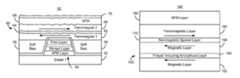
- the magnetic transducerincludes a shield 140 .
- FIG. 4is an ABS view of an exemplary embodiment of a portion of the shield 140 .
- the shield 140is a composite shield.
- the shield 140includes multiple layers and/or materials rather than being a single monolithic layer.
- the interfaces of the layers of the shield 140are smoother.
- the shield 140includes two ferromagnetic layers 150 and 180 separated by a nonmagnetic spacer layer 170 .
- the ferromagnetic layersare coupled antiparallel through the nonmagnetic spacer layer 170 , for example via an RKKY coupling.
- the nonmagnetic spacer layer 170may be Ru.
- the ferromagnetic 150 and 180may be NiFe.
- the shield 140also includes a pinning layer 190 , such as an AFM layer, that pins the magnetic moment of the ferromagnetic layer 180 .
- the pinning layer 190includes at least sixty and not more than three hundred Angstroms of IrMn.
- one ferromagnetic layer 150may be adjacent to the magnetic bias structures 130 , while the other ferromagnetic layer 180 is adjacent to the pinning layer 190 .
- the bottom ferromagnetic layer 150includes multiple magnetic layers interleaved with one or more trilayer structures 160 .
- the bottom ferromagnetic layer 150includes multiple magnetic layers interleaved with one or more trilayer structures 160 .
- two magnetic layers 152 and 154 and one trilayer structure 160are shown.
- another number of magnetic layers and a greater number of trilayer structuresmay be present.
- a trilayer within the shield 140includes at least three layers, but may include more than three layers.
- Each of the magnetic layers 152 and 154includes crystalline grains.
- the trilayer 160include one or more amorphous nonmagnetic layers (not shown in FIG. 4 ), each of which is less than three Angstroms thick.
- the amorphous nonmagnetic layerincludes one or more of Ta, Ti, Zr, W and Nb. Because the amorphous nonmagnetic layer is sufficiently thin, the magnetic layers 152 and 154 within the bottom ferromagnetic layer are ferromagnetically coupled. However, the trilayer 160 is also configured such that the crystalline grains in one magnetic layer 152 are decoupled from the crystalline grains in another magnetic layer 154 . In some embodiments, this decoupling is due to the presence of one or more amorphous layers in the trilayer 160 and/or the presence of multiple trilayers 160 .
- the presence of the trilayer(s)provides a smoother interface between the ferromagnetic layer 150 and the nonmagnetic spacer layer 170 .
- the trilayer 160is at least twenty Angstroms and not more than one hundred Angstroms from the nonmagnetic spacer layer 170 . Placing the trilayer 160 at this location may allow the trilayer 160 to break the crystalline grain growth in the magnetic layer 152 . Because the trilayer 160 includes amorphous layer(s), the top interface of the trilayer 160 may be smooth even though the bottom interface between the layers 152 and 160 may be rough due to grain growth in the magnetic layer 152 .
- This proximity to the nonmagnetic spacer layer 170means that the magnetic layer 154 is not more than one hundred Angstroms thick. Thus, the placement of the trilayer 160 may prevent the crystalline grain growth in the magnetic layer 154 from roughening the interface between the layers 150 and 170 .
- the nonmagnetic spacer layer 170is deposited on a smoother surface.
- the variation in thickness of the nonmagnetic spacer layer 170is, therefore, reduced.
- the magnetic coupling between the magnetic layers 150 and 180may be more uniform.
- the shield 140may be better stabilized. Performance of the magnetic read transducer 100 may thereby be enhanced.
- FIGS. 5-7depict exemplary embodiments of various trilayers 160 ′, 160 ′′ and 160 ′′′ that may be used for the trilayer 160 .
- FIGS. 5-7are not to scale.
- FIG. 5depicts a trilayer 160 ′ including two ferromagnetic layers 161 and 163 sandwiching the nonmagnetic amorphous layer 162 .
- the amorphous nonmagnetic layer 162consists of one or more of Ta, Ti, Zr, W and Nb. In some embodiments, the layer 162 may include B. As discussed above, the amorphous nonmagnetic layer 162 is thin. In some embodiments, the amorphous nonmagnetic layer 162 is less than three Angstroms thick.
- the magnetic layers 161 and 163may be ferromagnetically coupled through the amorphous nonmagnetic layer 162 .
- the magnetic layers 161 and 163include CoFe, CoFeB, and/or Co.
- the magnetic layers 161 and 163may be considered amorphous in some embodiments.
- the magnetic layers 161 and 163are also thin.
- the magnetic layers 161 and 163may be at least two Angstroms and not more than twenty Angstroms thick.
- the magnetic layers 161 and 163may be at least five and not more than ten Angstroms thick. At lower thicknesses, such as two Angstroms, the magnetic layers 161 and 163 may not be continuous.
- FIG. 6depicts a trilayer 160 ′′ including two nonmagnetic amorphous layers 162 and 164 sandwiching the magnetic layer 163 .
- Each of the amorphous nonmagnetic layers 162 and 164consists of one or more of Ta, Ti, Zr, W and Nb.
- the layer 162 and/or 164may include B.
- the amorphous nonmagnetic layers 162 and 164are thin.
- each of the amorphous nonmagnetic layers 162 and 164is less than three Angstroms thick.
- the magnetic layers in the ferromagnetic layer 150may be ferromagnetically coupled through the amorphous nonmagnetic layers 162 and 164 .
- the magnetic layer 161includes CoFe, CoFeB, and/or Co.
- the magnetic layer 161may be considered amorphous in some embodiments.
- the magnetic layer 161is also thin.
- the magnetic layer 161may be at least two Angstroms and not more than twenty Angstroms thick and, in some embodiments at least five and not more than ten Angstroms. At lower thicknesses, such as two Angstroms, the magnetic layer 161 may not be continuous.
- FIG. 7depicts a trilayer 160 ′′′ including three ferromagnetic layers 161 , 163 and 165 interleaved with nonmagnetic amorphous layers 162 and 164 .
- the “trilayer” 160 ′′′may be considered to consist of a trilayer 160 ′ plus a bilayer formed of layers 164 and 165 .
- Each of the amorphous nonmagnetic layers 162 and 164consists of one or more of Ta, Ti, Zr, W, Nb and B.
- the amorphous nonmagnetic layers 162 , 164 and 166are thin. In some embodiments, each of the amorphous nonmagnetic layers 162 , 164 and 166 is less than three Angstroms thick.
- the magnetic layers 161 , 163 and 165are ferromagnetically coupled through the amorphous nonmagnetic layers 162 and 164 .
- the magnetic layers 161 , 163 and 165include CoFe, CoFeB, and/or Co.
- the magnetic layers 161 , 163 and 1645may be considered amorphous in some embodiments.
- the magnetic layers 161 , 163 and 165are also thin.
- the magnetic layers 161 , 163 and 165may each be at least two Angstroms and not more than twenty Angstroms thick.
- each of the magnetic layers 161 , 163 and 165may be at least five and not more than ten Angstroms thick. Note that at lower thicknesses, such as two Angstroms, the magnetic layers 161 , 163 and 165 may not be continuous.
- three embodiments 160 ′, 160 ′′ and 160 ′′′ of trilayer 160are shown, other structures including another number of magnetic layers and amorphous nonmagnetic layers are possible.
- the trilayermay include two magnetic layers interleaved with two nonmagnetic amorphous layers.
- the outer layers of the trilayer 160need not be the same.
- the number amorphous nonmagnetic layers 162 and/or 164 includedmay depend upon the number of trilayers 160 used.
- a single trilayersuch as in the shield 140 depicted in FIG. 4
- at least two amorphous nonmagnetic layersmay be desired.
- the trilayer 160 ′′ or 160 ′′′may be preferred. This is because it may be desirable to have a total of more than four Angstroms of amorphous material in the ferromagnetic layer 150 of the shield.
- the number of amorphous nonmagnetic layers 162 and/or 164 providedneed not be accounted for.
- various trilayersincluding but not limited to the trilayers 160 ′, 160 ′′ and 160 ′′′ may be used in the shield 140 as the trilayer 160 . Because of the use of the trilayer 160 , 160 ′, 160 ′′ and/or 160 ′′′ the nonmagnetic spacer layer 170 is deposited on a smoother surface. The variation in thickness of the nonmagnetic spacer layer 170 is, therefore, reduced. The magnetic coupling between the magnetic layers 150 and 180 may be more uniform. Thus, the shield 140 may be better stabilized. Performance of the magnetic read transducer 100 may thereby be enhanced.
- FIG. 8depicts another exemplary embodiment of a magnetic shield 140 ′ that may be used in a read transducer such as the read transducer 100 .
- the shield 140 ′is a composite shield.
- the magnetic shield 140 ′is analogous to the magnetic shield 140 .
- the magnetic shield 140 ′thus includes ferromagnetic layers 150 ′ and 180 , nonmagnetic spacer layer 170 and pinning layer 190 that are analogous to ferromagnetic layers 150 and 180 , nonmagnetic spacer layer 170 and pinning layer 190 , respectively.
- the ferromagnetic layers 150 ′ and 180are coupled antiparallel through the nonmagnetic spacer layer 170 , for example via an RKKY coupling.
- the ferromagnetic layers 150 ′ and 180may include NiFe.
- the pinning layer 190includes at least sixty and not more than three hundred Angstroms of IrMn.
- the bottom ferromagnetic layer 150 ′includes multiple magnetic layers interleaved with two trilayers 160 .
- the bottom ferromagnetic layer 150 ′includes multiple magnetic layers interleaved with two trilayers 160 .
- three magnetic layers 152 ′, 154 ′ and 156 and two trilayers 160are shown.
- another number of magnetic layers and a different number of trilayersmay be present.
- trilayersare denoted with reference numeral 160 , the trilayers structures 160 ′, 160 ′′, 160 ′′′ and/or analogous trilayer structures might be used.
- Each of the magnetic layers 152 ′, 154 ′ and 156includes crystalline grains.
- the magnetic layers 152 ′, 154 ′ and 156include NiFe.
- the trilayers 160include one or more amorphous nonmagnetic layer(s), each of which is less than three Angstroms thick.
- the amorphous nonmagnetic layerincludes one or more of Ta, Ti, Zr, W, Nb and B. Because the amorphous nonmagnetic layer(s) are sufficiently thin, the magnetic layers 152 ′, 154 ′ and 156 within the ferromagnetic layer 150 ′ are ferromagnetically coupled.
- the trilayers 160are also configured such that the crystalline grains in the magnetic layers 152 ′, 154 ′ and 156 are decoupled from the crystalline grains in the other magnetic layers 152 ′, 154 ′ and 156 . This breaking of the coupling between crystalline grains may reduce the surface roughness of the layer 150 ′.
- the spacing of the trilayers 160may be selected to ensure that the magnetic layers 152 ′, 154 ′ and 156 have a reduced surface roughness.
- the ferromagnetic layer 150 ′is desired to have at least three hundred Angstroms of thickness of NiFe.
- the magnetic layers 152 ′ and 154 ′may then be at least one hundred and not more than two hundred Angstroms thick.
- the magnetic layer 156 closest to the nonmagnetic spacer layer 170may be desired to be thinner.
- the layer 156 closest to the nonmagnetic spacer layermay be at least twenty Angstroms thick and not more than one hundred Angstroms thick. However, in other embodiments, other thicknesses are possible.
- the presence of the trilayer(s) 160provides a smoother interface between the ferromagnetic layer 150 ′ and the nonmagnetic spacer layer 170 .
- the nonmagnetic spacer layer 170is, therefore, deposited on a smoother surface.
- the variation in thickness of the nonmagnetic spacer layer 170is reduced.
- the magnetic coupling between the magnetic layers 150 ′ and 180may be more uniform.
- the shield 140 ′may be better stabilized. Performance of the magnetic read transducer 100 may thereby be enhanced.
- FIG. 9depicts another exemplary embodiment of a magnetic shield 140 ′′ that may be used in a read transducer such as the read transducer 100 .
- the shield 140 ′′is a composite shield.
- the magnetic shield 140 ′′is analogous to the magnetic shields 140 and 140 ′.
- the magnetic shield 140 ′′thus includes ferromagnetic layers 150 ′′ and 180 , nonmagnetic spacer layer 170 and pinning layer 190 that are analogous to ferromagnetic layers 150 / 150 ′ and 180 , nonmagnetic spacer layer 170 and pinning layer 190 , respectively.
- the ferromagnetic layers 150 ′′ and 180are coupled antiparallel through the nonmagnetic spacer layer 170 , for example via an RKKY coupling.
- the ferromagnetic layers 150 ′′ and 180may include NiFe.
- the pinning layer 190includes at least sixty and not more than three hundred Angstroms of IrMn.
- the bottom ferromagnetic layer 150 ′′includes multiple magnetic layers interleaved with three trilayers 160 .
- three trilayers 160In the embodiment shown in FIG. 9 , four magnetic layers 152 ′′, 154 ′′, 156 ′ and 158 and three trilayers 160 are shown. However, another number of magnetic layers and a different number of trilayers may be present.
- trilayersare denoted with reference numeral 160 , the trilayers structures 160 ′, 160 ′′, 160 ′′′ and/or analogous trilayer structures might be used.
- Each of the magnetic layers 152 ′′, 154 ′′, 156 ′ and 158includes crystalline grains.
- the magnetic layers 152 ′′, 154 ′′, 156 ′ and 158include NiFe.
- the trilayers 160include one or more amorphous nonmagnetic layer(s), each of which is less than three Angstroms thick.
- the amorphous nonmagnetic layerincludes one or more of Ta, Ti, Zr, W, Nb and B. Because the amorphous nonmagnetic layer(s) are sufficiently thin, the magnetic layers 152 ′′, 154 ′′, 156 ′ and 158 within the ferromagnetic layer 150 are ferromagnetically coupled.
- the trilayers 160are also configured such that the crystalline grains in the magnetic layers 152 ′′, 154 ′′, 156 ′ and 158 are decoupled from the crystalline grains in the other magnetic layers 152 ′′, 154 ′′, 156 ′ and 158 . This breaking of the coupling between crystalline grains may reduce the surface roughness of the layer 150 ′′.
- the spacing of the trilayers 160may be selected to ensure that the magnetic layers 152 ′′, 154 ′′, 156 ′ and 158 have a reduced surface roughness.
- the ferromagnetic layer 150 ′′is desired to have at least three hundred Angstroms of thickness of NiFe.
- the magnetic layers 152 ′′, 154 ′′ and 156 ′may then be at least one hundred and not more than one hundred and fifty Angstroms thick.
- the magnetic layer 158 closest to the nonmagnetic spacer layer 170may be desired to be thinner.
- the layer 158 closest to the nonmagnetic spacer layermay be at least twenty Angstroms thick and not more than one hundred Angstroms thick. However, in other embodiments, other thicknesses are possible.
- the presence of the trilayer(s) 160provides a smoother interface between the ferromagnetic layer 150 ′′ and the nonmagnetic spacer layer 170 .
- the nonmagnetic spacer layer 170is, therefore, deposited on a smoother surface.
- the variation in thickness of the nonmagnetic spacer layer 170is reduced.
- the magnetic coupling between the magnetic layers 150 ′′ and 180may be more uniform.
- the shield 140 ′′may be better stabilized. Performance of the magnetic read transducer 100 may thereby be enhanced.
- FIG. 10depicts another exemplary embodiment of a magnetic shield 140 ′′′ that may be used in a read transducer such as the read transducer 100 .
- the shield 140 ′′′is a composite shield.
- the magnetic shield 140 ′′is analogous to the magnetic shields 140 , 140 ′ and 140 ′′.
- the magnetic shield 140 ′′′thus includes ferromagnetic layers 150 ′′ and 180 ′, nonmagnetic spacer layer 170 and pinning layer 190 that are analogous to ferromagnetic layers 150 / 150 ′/ 150 ′′ and 180 , nonmagnetic spacer layer 170 and pinning layer 190 , respectively.
- the ferromagnetic layers 150 ′′′ and 180 ′are coupled antiparallel through the nonmagnetic spacer layer 170 , for example via an RKKY coupling.
- the ferromagnetic layers 150 ′′′ and 180 ′may include NiFe.
- the pinning layer 190includes at least sixty and not more than three hundred Angstroms of IrMn.
- the bottom ferromagnetic layer 150 ′′is substantially the same as depicted in FIG. 9 .
- other ferromagnetic layersincluding but not limited to 150 and 150 ′ may be used.
- the layer 150 ′′includes multiple magnetic layers 152 ′′, 154 ′′, 156 ′ and 158 interleaved with trilayers 160 .
- the ferromagnetic layer 150 ′′has a smoother surface for reasons analogous to those discussed above.
- the ferromagnetic layer 180 ′includes magnetic layers 182 and 184 interleaved with trilayer 160 .
- the magnetic layers 182 and 184include NiFe.
- the trilayers 160 ′, 160 ′′, 160 ′′′ or an analogous trilayermay be used for the trilayer 160 .
- the magnetic layers 182 and 184each include crystalline grains.
- the trilayer 160includes one or more amorphous nonmagnetic layer(s), each of which is less than three Angstroms thick.
- the amorphous nonmagnetic layerincludes one or more of Ta, Ti, Zr, W, Nb and B. Because the amorphous nonmagnetic layer(s) are sufficiently thin, the magnetic layers 182 and 184 within the ferromagnetic layer 180 ′ are ferromagnetically coupled.
- the trilayers 160are also configured such that the crystalline grains in the magnetic layers 182 and 184 are decoupled from the crystalline grains in the other magnetic layers 182 and 184 . This breaking of the coupling between crystalline grains may reduce the surface roughness of the layer 180 ′.
- additional trilayers 160 and nonmagnetic layersmay be included in the ferromagnetic layer 180 ′.
- the presence of the trilayer(s) 160provides a smoother interface between the ferromagnetic layer 150 ′′ and the nonmagnetic spacer layer 170 .
- the variation in thickness of the nonmagnetic spacer layer 170may be reduced and the magnetic coupling between the magnetic layers 150 ′′ and 180 ′ may be more uniform.
- the shield 140 ′′′may be better stabilized.
- the surface roughness of the magnetic layer 180 ′may be reduced.
- subsequent layerssuch as the AFM layer 190 and capping layer 192 may be smoother. Performance of the magnetic read transducer 100 may thereby be enhanced.
- FIG. 11is an exemplary embodiment of a method 200 for providing a read transducer including a composite shield. For simplicity, some steps may be omitted, interleaved, and/or combined.
- the method 200is also described in the context of providing a single recording transducer 100 and shield 140 depicted in FIGS. 3-4 . However, the method 200 may be used to fabricate multiple transducers at substantially the same time.
- the method 200may also be used to fabricate other shields including but not limited to any combination of 140 ′, 140 ′′ and/or 140 ′′′ using the trilayers 160 , 160 ′, 160 ′′ and/or 160 ′′′.
- the method 200is also described in the context of particular layers. A particular layer may include multiple materials and/or multiple sub-layers.
- the method 200also may start after formation of other portions of the magnetic recording transducer.
- the first shield 102is provided, via step 202 .
- Step 202typically includes depositing a large high permeability layer.
- the sensor 110is provided, via step 204 .
- Step 204typically includes depositing the layers for the sensor 110 , then defining the sensor 110 in at least the track width direction using an ion mill. In some embodiments, the free layer 118 and pinned layer 114 of the sensor 110 are also defined in the stripe height direction.
- the magnetic bias structures 130are provided, via step 206 .
- the magnetic bias structures 130may be soft magnetic bias structures.
- Step 206may thus include depositing the high permeability and any other material(s) for the magnetic bias structures 130 and defining the magnetic bias structures 130 in the track width and stripe height direction.
- portions of steps 204 and 206are interleaved.
- portions of the sensor 110may be defined in the stripe height direction as the soft magnetic bias structures are defined in the stripe height direction.
- Step 206may also include depositing multiple layers for the soft magnetic bias structures 130 .
- the soft magnetic bias structures 130are provided such that they may be magnetically coupled to the shield 102 and/or 140 .
- the shield 140is provided in steps 208 , 210 , 212 , 214 and 216 .
- steps 208 , 210 , 212 , 214 and 216are performed as a single processing block in a single deposition system.
- the ferromagnetic layer 150 including trilayer(s) 160 and magnetic layers 152 and 154are provided, via step 208 .
- NiFe layerssuch as layers 152 / 152 ′, 154 / 154 ′, 156 ′/ 156 ′ and 158 are provided along with trilayer(s) 160 .
- the magnetic layers 152 / 152 ′, 154 / 154 ′, 156 ′/ 156 ′ and 158are ferromagnetically coupled.
- the crystallographic grains of the magnetic layers 152 / 152 ′, 154 / 154 ′, 156 ′/ 156 ′ and 158are decoupled.
- the nonmagnetic spacer layer 170is provided, via step 210 .
- Step 210may thus include depositing a Ru layer.
- the second ferromagnetic layer 180 / 180 ′is provided, via step 212 .
- step 212includes depositing a magnetic layer such as the layer 180 .
- step 212may optionally include providing a ferromagnetic layer 180 ′ including trilayers 160 and magnetic layers 182 and 184 , or an analogous ferromagnetic layer.
- NiFe layerssuch as layers 182 and 182 may be provided along with trilayer(s) 160 .
- the magnetic layers 182 and 184are ferromagnetically coupled.
- the crystallographic grains of the magnetic layers 182 and 184are decoupled.
- a pinning layer such as the layer 190may be provided, via step 214 .
- step 214may include depositing a layer of IrMn.
- a capping layer 192for example Ru and/or Ta, may also be provided, via step 214 . Fabrication of the transducer 100 may then be completed.
- the transducers 100 including a composite shield such as the shields 140 , 140 ′, 140 ′′ or 140 ′′′may be fabricated.
- the benefits of the transducer 100 and one or more of the shields 140 , 140 ′, 140 ′′ and/or 140 ′′′may be achieved.
Landscapes
- Engineering & Computer Science (AREA)
- Manufacturing & Machinery (AREA)
- Chemical & Material Sciences (AREA)
- Nanotechnology (AREA)
- Physics & Mathematics (AREA)
- Mathematical Physics (AREA)
- Theoretical Computer Science (AREA)
- Crystallography & Structural Chemistry (AREA)
- Magnetic Heads (AREA)
- Hall/Mr Elements (AREA)
Abstract
Description
Claims (19)
Priority Applications (1)
| Application Number | Priority Date | Filing Date | Title |
|---|---|---|---|
| US13/723,099US8531801B1 (en) | 2012-12-20 | 2012-12-20 | Method and system for providing a read transducer having a composite magnetic shield with smooth interfaces |
Applications Claiming Priority (1)
| Application Number | Priority Date | Filing Date | Title |
|---|---|---|---|
| US13/723,099US8531801B1 (en) | 2012-12-20 | 2012-12-20 | Method and system for providing a read transducer having a composite magnetic shield with smooth interfaces |
Publications (1)
| Publication Number | Publication Date |
|---|---|
| US8531801B1true US8531801B1 (en) | 2013-09-10 |
Family
ID=49084147
Family Applications (1)
| Application Number | Title | Priority Date | Filing Date |
|---|---|---|---|
| US13/723,099ActiveUS8531801B1 (en) | 2012-12-20 | 2012-12-20 | Method and system for providing a read transducer having a composite magnetic shield with smooth interfaces |
Country Status (1)
| Country | Link |
|---|---|
| US (1) | US8531801B1 (en) |
Cited By (156)
| Publication number | Priority date | Publication date | Assignee | Title |
|---|---|---|---|---|
| US8675318B1 (en) | 2011-11-22 | 2014-03-18 | Western Digital (Fremont), Llc | Method and system for providing a read transducer having a reduced shield-to-shield spacing |
| US8711528B1 (en) | 2012-06-29 | 2014-04-29 | Western Digital (Fremont), Llc | Tunnel magnetoresistance read head with narrow shield-to-shield spacing |
| US8760822B1 (en)* | 2012-11-28 | 2014-06-24 | Western Digital (Fremont), Llc | Method and system for providing a read transducer having an extended pinned layer and soft magnetic bias structures with improved stability |
| US8760819B1 (en) | 2010-12-23 | 2014-06-24 | Western Digital (Fremont), Llc | Magnetic recording sensor with sputtered antiferromagnetic coupling trilayer between plated ferromagnetic shields |
| US8780505B1 (en)* | 2013-03-12 | 2014-07-15 | Western Digital (Fremont), Llc | Method and system for providing a read transducer having an improved composite magnetic shield |
| US8797692B1 (en) | 2012-09-07 | 2014-08-05 | Western Digital (Fremont), Llc | Magnetic recording sensor with AFM exchange coupled shield stabilization |
| US8830628B1 (en) | 2009-02-23 | 2014-09-09 | Western Digital (Fremont), Llc | Method and system for providing a perpendicular magnetic recording head |
| US8879207B1 (en) | 2011-12-20 | 2014-11-04 | Western Digital (Fremont), Llc | Method for providing a side shield for a magnetic recording transducer using an air bridge |
| US8883017B1 (en) | 2013-03-12 | 2014-11-11 | Western Digital (Fremont), Llc | Method and system for providing a read transducer having seamless interfaces |
| US8917581B1 (en) | 2013-12-18 | 2014-12-23 | Western Digital Technologies, Inc. | Self-anneal process for a near field transducer and chimney in a hard disk drive assembly |
| US8923102B1 (en) | 2013-07-16 | 2014-12-30 | Western Digital (Fremont), Llc | Optical grating coupling for interferometric waveguides in heat assisted magnetic recording heads |
| US8947985B1 (en) | 2013-07-16 | 2015-02-03 | Western Digital (Fremont), Llc | Heat assisted magnetic recording transducers having a recessed pole |
| US20150036246A1 (en)* | 2013-07-30 | 2015-02-05 | Seagate Technology Llc | Magnetoresistive sensor shield |
| US20150036245A1 (en)* | 2013-07-31 | 2015-02-05 | Seagate Technology Llc | Magnetoresistive sensor |
| US8953422B1 (en) | 2014-06-10 | 2015-02-10 | Western Digital (Fremont), Llc | Near field transducer using dielectric waveguide core with fine ridge feature |
| US8958272B1 (en) | 2014-06-10 | 2015-02-17 | Western Digital (Fremont), Llc | Interfering near field transducer for energy assisted magnetic recording |
| US8970988B1 (en) | 2013-12-31 | 2015-03-03 | Western Digital (Fremont), Llc | Electric gaps and method for making electric gaps for multiple sensor arrays |
| US8971160B1 (en) | 2013-12-19 | 2015-03-03 | Western Digital (Fremont), Llc | Near field transducer with high refractive index pin for heat assisted magnetic recording |
| US8970994B2 (en) | 2013-03-08 | 2015-03-03 | Seagate Technology Llc | Reader with decoupled magnetic seed layer |
| US20150062755A1 (en)* | 2013-08-28 | 2015-03-05 | Seagate Technology Llc | Dual reader structure |
| US8976635B1 (en) | 2014-06-10 | 2015-03-10 | Western Digital (Fremont), Llc | Near field transducer driven by a transverse electric waveguide for energy assisted magnetic recording |
| US8980109B1 (en) | 2012-12-11 | 2015-03-17 | Western Digital (Fremont), Llc | Method for providing a magnetic recording transducer using a combined main pole and side shield CMP for a wraparound shield scheme |
| US8982508B1 (en) | 2011-10-31 | 2015-03-17 | Western Digital (Fremont), Llc | Method for providing a side shield for a magnetic recording transducer |
| US8984740B1 (en) | 2012-11-30 | 2015-03-24 | Western Digital (Fremont), Llc | Process for providing a magnetic recording transducer having a smooth magnetic seed layer |
| US8988825B1 (en) | 2014-02-28 | 2015-03-24 | Western Digital (Fremont, LLC | Method for fabricating a magnetic writer having half-side shields |
| US8988812B1 (en) | 2013-11-27 | 2015-03-24 | Western Digital (Fremont), Llc | Multi-sensor array configuration for a two-dimensional magnetic recording (TDMR) operation |
| US8993217B1 (en) | 2013-04-04 | 2015-03-31 | Western Digital (Fremont), Llc | Double exposure technique for high resolution disk imaging |
| US8995087B1 (en) | 2006-11-29 | 2015-03-31 | Western Digital (Fremont), Llc | Perpendicular magnetic recording write head having a wrap around shield |
| US9001628B1 (en) | 2013-12-16 | 2015-04-07 | Western Digital (Fremont), Llc | Assistant waveguides for evaluating main waveguide coupling efficiency and diode laser alignment tolerances for hard disk |
| US9001467B1 (en) | 2014-03-05 | 2015-04-07 | Western Digital (Fremont), Llc | Method for fabricating side shields in a magnetic writer |
| US8997832B1 (en) | 2010-11-23 | 2015-04-07 | Western Digital (Fremont), Llc | Method of fabricating micrometer scale components |
| US9007879B1 (en) | 2014-06-10 | 2015-04-14 | Western Digital (Fremont), Llc | Interfering near field transducer having a wide metal bar feature for energy assisted magnetic recording |
| US9007719B1 (en) | 2013-10-23 | 2015-04-14 | Western Digital (Fremont), Llc | Systems and methods for using double mask techniques to achieve very small features |
| US9007725B1 (en) | 2014-10-07 | 2015-04-14 | Western Digital (Fremont), Llc | Sensor with positive coupling between dual ferromagnetic free layer laminates |
| US9013836B1 (en) | 2013-04-02 | 2015-04-21 | Western Digital (Fremont), Llc | Method and system for providing an antiferromagnetically coupled return pole |
| US9042208B1 (en) | 2013-03-11 | 2015-05-26 | Western Digital Technologies, Inc. | Disk drive measuring fly height by applying a bias voltage to an electrically insulated write component of a head |
| US9042051B2 (en) | 2013-08-15 | 2015-05-26 | Western Digital (Fremont), Llc | Gradient write gap for perpendicular magnetic recording writer |
| US9042052B1 (en) | 2014-06-23 | 2015-05-26 | Western Digital (Fremont), Llc | Magnetic writer having a partially shunted coil |
| US9042058B1 (en) | 2013-10-17 | 2015-05-26 | Western Digital Technologies, Inc. | Shield designed for middle shields in a multiple sensor array |
| US9042057B1 (en) | 2013-01-09 | 2015-05-26 | Western Digital (Fremont), Llc | Methods for providing magnetic storage elements with high magneto-resistance using Heusler alloys |
| US9053735B1 (en) | 2014-06-20 | 2015-06-09 | Western Digital (Fremont), Llc | Method for fabricating a magnetic writer using a full-film metal planarization |
| CN104715765A (en)* | 2013-12-13 | 2015-06-17 | 希捷科技有限公司 | Magnetoresistive sensor shield |
| US9064507B1 (en) | 2009-07-31 | 2015-06-23 | Western Digital (Fremont), Llc | Magnetic etch-stop layer for magnetoresistive read heads |
| US9064527B1 (en) | 2013-04-12 | 2015-06-23 | Western Digital (Fremont), Llc | High order tapered waveguide for use in a heat assisted magnetic recording head |
| US9064528B1 (en) | 2013-05-17 | 2015-06-23 | Western Digital Technologies, Inc. | Interferometric waveguide usable in shingled heat assisted magnetic recording in the absence of a near-field transducer |
| US9070381B1 (en) | 2013-04-12 | 2015-06-30 | Western Digital (Fremont), Llc | Magnetic recording read transducer having a laminated free layer |
| US9082423B1 (en) | 2013-12-18 | 2015-07-14 | Western Digital (Fremont), Llc | Magnetic recording write transducer having an improved trailing surface profile |
| US9087527B1 (en) | 2014-10-28 | 2015-07-21 | Western Digital (Fremont), Llc | Apparatus and method for middle shield connection in magnetic recording transducers |
| US9087534B1 (en) | 2011-12-20 | 2015-07-21 | Western Digital (Fremont), Llc | Method and system for providing a read transducer having soft and hard magnetic bias structures |
| US9093639B2 (en) | 2012-02-21 | 2015-07-28 | Western Digital (Fremont), Llc | Methods for manufacturing a magnetoresistive structure utilizing heating and cooling |
| US9104107B1 (en) | 2013-04-03 | 2015-08-11 | Western Digital (Fremont), Llc | DUV photoresist process |
| US9111550B1 (en) | 2014-12-04 | 2015-08-18 | Western Digital (Fremont), Llc | Write transducer having a magnetic buffer layer spaced between a side shield and a write pole by non-magnetic layers |
| US9111564B1 (en) | 2013-04-02 | 2015-08-18 | Western Digital (Fremont), Llc | Magnetic recording writer having a main pole with multiple flare angles |
| US9111558B1 (en) | 2014-03-14 | 2015-08-18 | Western Digital (Fremont), Llc | System and method of diffractive focusing of light in a waveguide |
| US9123362B1 (en) | 2011-03-22 | 2015-09-01 | Western Digital (Fremont), Llc | Methods for assembling an electrically assisted magnetic recording (EAMR) head |
| US9123358B1 (en) | 2012-06-11 | 2015-09-01 | Western Digital (Fremont), Llc | Conformal high moment side shield seed layer for perpendicular magnetic recording writer |
| US9123374B1 (en) | 2015-02-12 | 2015-09-01 | Western Digital (Fremont), Llc | Heat assisted magnetic recording writer having an integrated polarization rotation plate |
| US9123359B1 (en) | 2010-12-22 | 2015-09-01 | Western Digital (Fremont), Llc | Magnetic recording transducer with sputtered antiferromagnetic coupling trilayer between plated ferromagnetic shields and method of fabrication |
| US20150248903A1 (en)* | 2014-02-28 | 2015-09-03 | HGST Netherlands B.V. | Af-coupled dual side shield reader with af-coupled usl |
| US9135930B1 (en) | 2014-03-06 | 2015-09-15 | Western Digital (Fremont), Llc | Method for fabricating a magnetic write pole using vacuum deposition |
| US9135937B1 (en) | 2014-05-09 | 2015-09-15 | Western Digital (Fremont), Llc | Current modulation on laser diode for energy assisted magnetic recording transducer |
| US9142233B1 (en) | 2014-02-28 | 2015-09-22 | Western Digital (Fremont), Llc | Heat assisted magnetic recording writer having a recessed pole |
| US9147404B1 (en) | 2015-03-31 | 2015-09-29 | Western Digital (Fremont), Llc | Method and system for providing a read transducer having a dual free layer |
| US9147408B1 (en) | 2013-12-19 | 2015-09-29 | Western Digital (Fremont), Llc | Heated AFM layer deposition and cooling process for TMR magnetic recording sensor with high pinning field |
| US9153255B1 (en) | 2014-03-05 | 2015-10-06 | Western Digital (Fremont), Llc | Method for fabricating a magnetic writer having an asymmetric gap and shields |
| US9183854B2 (en) | 2014-02-24 | 2015-11-10 | Western Digital (Fremont), Llc | Method to make interferometric taper waveguide for HAMR light delivery |
| US9190079B1 (en) | 2014-09-22 | 2015-11-17 | Western Digital (Fremont), Llc | Magnetic write pole having engineered radius of curvature and chisel angle profiles |
| US9190078B2 (en) | 2013-08-30 | 2015-11-17 | Seagate Technology Llc | Dual reader structure |
| US9190085B1 (en) | 2014-03-12 | 2015-11-17 | Western Digital (Fremont), Llc | Waveguide with reflective grating for localized energy intensity |
| US9194692B1 (en) | 2013-12-06 | 2015-11-24 | Western Digital (Fremont), Llc | Systems and methods for using white light interferometry to measure undercut of a bi-layer structure |
| US9202493B1 (en) | 2014-02-28 | 2015-12-01 | Western Digital (Fremont), Llc | Method of making an ultra-sharp tip mode converter for a HAMR head |
| US9202480B2 (en) | 2009-10-14 | 2015-12-01 | Western Digital (Fremont), LLC. | Double patterning hard mask for damascene perpendicular magnetic recording (PMR) writer |
| US9214172B2 (en) | 2013-10-23 | 2015-12-15 | Western Digital (Fremont), Llc | Method of manufacturing a magnetic read head |
| US9214169B1 (en)* | 2014-06-20 | 2015-12-15 | Western Digital (Fremont), Llc | Magnetic recording read transducer having a laminated free layer |
| US9213322B1 (en) | 2012-08-16 | 2015-12-15 | Western Digital (Fremont), Llc | Methods for providing run to run process control using a dynamic tuner |
| US9214165B1 (en) | 2014-12-18 | 2015-12-15 | Western Digital (Fremont), Llc | Magnetic writer having a gradient in saturation magnetization of the shields |
| US9230565B1 (en) | 2014-06-24 | 2016-01-05 | Western Digital (Fremont), Llc | Magnetic shield for magnetic recording head |
| US9236560B1 (en) | 2014-12-08 | 2016-01-12 | Western Digital (Fremont), Llc | Spin transfer torque tunneling magnetoresistive device having a laminated free layer with perpendicular magnetic anisotropy |
| US9245545B1 (en) | 2013-04-12 | 2016-01-26 | Wester Digital (Fremont), Llc | Short yoke length coils for magnetic heads in disk drives |
| US9245562B1 (en) | 2015-03-30 | 2016-01-26 | Western Digital (Fremont), Llc | Magnetic recording writer with a composite main pole |
| US9245543B1 (en) | 2010-06-25 | 2016-01-26 | Western Digital (Fremont), Llc | Method for providing an energy assisted magnetic recording head having a laser integrally mounted to the slider |
| US9251813B1 (en) | 2009-04-19 | 2016-02-02 | Western Digital (Fremont), Llc | Method of making a magnetic recording head |
| US9263067B1 (en) | 2013-05-29 | 2016-02-16 | Western Digital (Fremont), Llc | Process for making PMR writer with constant side wall angle |
| US9263071B1 (en) | 2015-03-31 | 2016-02-16 | Western Digital (Fremont), Llc | Flat NFT for heat assisted magnetic recording |
| US9269382B1 (en) | 2012-06-29 | 2016-02-23 | Western Digital (Fremont), Llc | Method and system for providing a read transducer having improved pinning of the pinned layer at higher recording densities |
| US9275657B1 (en) | 2013-08-14 | 2016-03-01 | Western Digital (Fremont), Llc | Process for making PMR writer with non-conformal side gaps |
| US9280990B1 (en) | 2013-12-11 | 2016-03-08 | Western Digital (Fremont), Llc | Method for fabricating a magnetic writer using multiple etches |
| US9287494B1 (en) | 2013-06-28 | 2016-03-15 | Western Digital (Fremont), Llc | Magnetic tunnel junction (MTJ) with a magnesium oxide tunnel barrier |
| US9286919B1 (en) | 2014-12-17 | 2016-03-15 | Western Digital (Fremont), Llc | Magnetic writer having a dual side gap |
| US9305583B1 (en) | 2014-02-18 | 2016-04-05 | Western Digital (Fremont), Llc | Method for fabricating a magnetic writer using multiple etches of damascene materials |
| US9312064B1 (en) | 2015-03-02 | 2016-04-12 | Western Digital (Fremont), Llc | Method to fabricate a magnetic head including ion milling of read gap using dual layer hard mask |
| US9318130B1 (en) | 2013-07-02 | 2016-04-19 | Western Digital (Fremont), Llc | Method to fabricate tunneling magnetic recording heads with extended pinned layer |
| GB2531906A (en)* | 2014-01-28 | 2016-05-04 | HGST Netherlands BV | A dual capping layer utilized in a magnetoresistive effect sensor |
| US9336814B1 (en) | 2013-03-12 | 2016-05-10 | Western Digital (Fremont), Llc | Inverse tapered waveguide for use in a heat assisted magnetic recording head |
| US9343087B1 (en) | 2014-12-21 | 2016-05-17 | Western Digital (Fremont), Llc | Method for fabricating a magnetic writer having half shields |
| US9343086B1 (en) | 2013-09-11 | 2016-05-17 | Western Digital (Fremont), Llc | Magnetic recording write transducer having an improved sidewall angle profile |
| US9343098B1 (en) | 2013-08-23 | 2016-05-17 | Western Digital (Fremont), Llc | Method for providing a heat assisted magnetic recording transducer having protective pads |
| US9349392B1 (en) | 2012-05-24 | 2016-05-24 | Western Digital (Fremont), Llc | Methods for improving adhesion on dielectric substrates |
| US9349394B1 (en) | 2013-10-18 | 2016-05-24 | Western Digital (Fremont), Llc | Method for fabricating a magnetic writer having a gradient side gap |
| US9361914B1 (en) | 2014-06-18 | 2016-06-07 | Western Digital (Fremont), Llc | Magnetic sensor with thin capping layer |
| US9361913B1 (en) | 2013-06-03 | 2016-06-07 | Western Digital (Fremont), Llc | Recording read heads with a multi-layer AFM layer methods and apparatuses |
| US9368134B1 (en) | 2010-12-16 | 2016-06-14 | Western Digital (Fremont), Llc | Method and system for providing an antiferromagnetically coupled writer |
| US9384765B1 (en) | 2015-09-24 | 2016-07-05 | Western Digital (Fremont), Llc | Method and system for providing a HAMR writer having improved optical efficiency |
| US9384764B1 (en) | 2015-06-27 | 2016-07-05 | International Business Machines Corporation | Electrically conductive magnetic shield laminate structure for contact recording sensor |
| US9384763B1 (en) | 2015-03-26 | 2016-07-05 | Western Digital (Fremont), Llc | Dual free layer magnetic reader having a rear bias structure including a soft bias layer |
| US9396743B1 (en) | 2014-02-28 | 2016-07-19 | Western Digital (Fremont), Llc | Systems and methods for controlling soft bias thickness for tunnel magnetoresistance readers |
| US9396742B1 (en) | 2012-11-30 | 2016-07-19 | Western Digital (Fremont), Llc | Magnetoresistive sensor for a magnetic storage system read head, and fabrication method thereof |
| US9406319B1 (en)* | 2015-06-27 | 2016-08-02 | International Business Machines Corporation | Electrically non-conductive magnetic shield laminate structure for contact recording sensor |
| US9406331B1 (en) | 2013-06-17 | 2016-08-02 | Western Digital (Fremont), Llc | Method for making ultra-narrow read sensor and read transducer device resulting therefrom |
| US9424866B1 (en) | 2015-09-24 | 2016-08-23 | Western Digital (Fremont), Llc | Heat assisted magnetic recording write apparatus having a dielectric gap |
| US9431031B1 (en) | 2015-03-24 | 2016-08-30 | Western Digital (Fremont), Llc | System and method for magnetic transducers having multiple sensors and AFC shields |
| US9431038B1 (en) | 2015-06-29 | 2016-08-30 | Western Digital (Fremont), Llc | Method for fabricating a magnetic write pole having an improved sidewall angle profile |
| US9431047B1 (en) | 2013-05-01 | 2016-08-30 | Western Digital (Fremont), Llc | Method for providing an improved AFM reader shield |
| US9431032B1 (en) | 2013-08-14 | 2016-08-30 | Western Digital (Fremont), Llc | Electrical connection arrangement for a multiple sensor array usable in two-dimensional magnetic recording |
| US9431039B1 (en) | 2013-05-21 | 2016-08-30 | Western Digital (Fremont), Llc | Multiple sensor array usable in two-dimensional magnetic recording |
| US9437251B1 (en) | 2014-12-22 | 2016-09-06 | Western Digital (Fremont), Llc | Apparatus and method having TDMR reader to reader shunts |
| US9443541B1 (en) | 2015-03-24 | 2016-09-13 | Western Digital (Fremont), Llc | Magnetic writer having a gradient in saturation magnetization of the shields and return pole |
| US9441938B1 (en) | 2013-10-08 | 2016-09-13 | Western Digital (Fremont), Llc | Test structures for measuring near field transducer disc length |
| US9449621B1 (en) | 2015-03-26 | 2016-09-20 | Western Digital (Fremont), Llc | Dual free layer magnetic reader having a rear bias structure having a high aspect ratio |
| US9449625B1 (en) | 2014-12-24 | 2016-09-20 | Western Digital (Fremont), Llc | Heat assisted magnetic recording head having a plurality of diffusion barrier layers |
| US9454979B1 (en)* | 2014-11-14 | 2016-09-27 | Seagate Technology Llc | Sensor structure with multilayer top shield |
| US9472216B1 (en) | 2015-09-23 | 2016-10-18 | Western Digital (Fremont), Llc | Differential dual free layer magnetic reader |
| US9484051B1 (en) | 2015-11-09 | 2016-11-01 | The Provost, Fellows, Foundation Scholars and the other members of Board, of the College of the Holy and Undivided Trinity of Queen Elizabeth near Dublin | Method and system for reducing undesirable reflections in a HAMR write apparatus |
| US9508365B1 (en) | 2015-06-24 | 2016-11-29 | Western Digital (Fremont), LLC. | Magnetic reader having a crystal decoupling structure |
| US9508363B1 (en) | 2014-06-17 | 2016-11-29 | Western Digital (Fremont), Llc | Method for fabricating a magnetic write pole having a leading edge bevel |
| US9508372B1 (en) | 2015-06-03 | 2016-11-29 | Western Digital (Fremont), Llc | Shingle magnetic writer having a low sidewall angle pole |
| US9530443B1 (en) | 2015-06-25 | 2016-12-27 | Western Digital (Fremont), Llc | Method for fabricating a magnetic recording device having a high aspect ratio structure |
| US9564150B1 (en) | 2015-11-24 | 2017-02-07 | Western Digital (Fremont), Llc | Magnetic read apparatus having an improved read sensor isolation circuit |
| US9595273B1 (en) | 2015-09-30 | 2017-03-14 | Western Digital (Fremont), Llc | Shingle magnetic writer having nonconformal shields |
| US9646639B2 (en) | 2015-06-26 | 2017-05-09 | Western Digital (Fremont), Llc | Heat assisted magnetic recording writer having integrated polarization rotation waveguides |
| US9666214B1 (en) | 2015-09-23 | 2017-05-30 | Western Digital (Fremont), Llc | Free layer magnetic reader that may have a reduced shield-to-shield spacing |
| US9685177B2 (en)* | 2015-07-08 | 2017-06-20 | Seagate Technology Llc | Sensor stabilization in a multiple sensor magnetic reproducing device |
| US9721595B1 (en) | 2014-12-04 | 2017-08-01 | Western Digital (Fremont), Llc | Method for providing a storage device |
| US9740805B1 (en) | 2015-12-01 | 2017-08-22 | Western Digital (Fremont), Llc | Method and system for detecting hotspots for photolithographically-defined devices |
| US9741366B1 (en) | 2014-12-18 | 2017-08-22 | Western Digital (Fremont), Llc | Method for fabricating a magnetic writer having a gradient in saturation magnetization of the shields |
| US9754611B1 (en) | 2015-11-30 | 2017-09-05 | Western Digital (Fremont), Llc | Magnetic recording write apparatus having a stepped conformal trailing shield |
| US9767831B1 (en) | 2015-12-01 | 2017-09-19 | Western Digital (Fremont), Llc | Magnetic writer having convex trailing surface pole and conformal write gap |
| US9786301B1 (en) | 2014-12-02 | 2017-10-10 | Western Digital (Fremont), Llc | Apparatuses and methods for providing thin shields in a multiple sensor array |
| US9799351B1 (en) | 2015-11-30 | 2017-10-24 | Western Digital (Fremont), Llc | Short yoke length writer having assist coils |
| US9812155B1 (en) | 2015-11-23 | 2017-11-07 | Western Digital (Fremont), Llc | Method and system for fabricating high junction angle read sensors |
| US9842615B1 (en) | 2015-06-26 | 2017-12-12 | Western Digital (Fremont), Llc | Magnetic reader having a nonmagnetic insertion layer for the pinning layer |
| US9858951B1 (en) | 2015-12-01 | 2018-01-02 | Western Digital (Fremont), Llc | Method for providing a multilayer AFM layer in a read sensor |
| US9881638B1 (en) | 2014-12-17 | 2018-01-30 | Western Digital (Fremont), Llc | Method for providing a near-field transducer (NFT) for a heat assisted magnetic recording (HAMR) device |
| US9934811B1 (en) | 2014-03-07 | 2018-04-03 | Western Digital (Fremont), Llc | Methods for controlling stray fields of magnetic features using magneto-elastic anisotropy |
| US9940956B1 (en)* | 2016-06-30 | 2018-04-10 | Western Digital (Fremont), Llc | Apparatus and method for reducing corrosion in capping layer of magnetic recording reader |
| US9953670B1 (en) | 2015-11-10 | 2018-04-24 | Western Digital (Fremont), Llc | Method and system for providing a HAMR writer including a multi-mode interference device |
| US9997180B1 (en) | 2017-03-22 | 2018-06-12 | International Business Machines Corporation | Hybrid dielectric gap liner and magnetic shield liner |
| US10037770B1 (en) | 2015-11-12 | 2018-07-31 | Western Digital (Fremont), Llc | Method for providing a magnetic recording write apparatus having a seamless pole |
| US10074387B1 (en) | 2014-12-21 | 2018-09-11 | Western Digital (Fremont), Llc | Method and system for providing a read transducer having symmetric antiferromagnetically coupled shields |
| US10090008B2 (en) | 2015-06-15 | 2018-10-02 | Seagate Technology Llc | Magnetoresistive sensor fabrication |
| US10354682B2 (en) | 2016-02-02 | 2019-07-16 | Seagate Technology Llc | Thin data reader cap |
| US10803889B2 (en) | 2019-02-21 | 2020-10-13 | International Business Machines Corporation | Apparatus with data reader sensors more recessed than servo reader sensor |
| US11074930B1 (en) | 2020-05-11 | 2021-07-27 | International Business Machines Corporation | Read transducer structure having an embedded wear layer between thin and thick shield portions |
| US11114117B1 (en) | 2020-05-20 | 2021-09-07 | International Business Machines Corporation | Process for manufacturing magnetic head having a servo read transducer structure with dielectric gap liner and a data read transducer structure with an embedded wear layer between thin and thick shield portions |
| CN113889153A (en)* | 2020-07-01 | 2022-01-04 | 西部数据技术公司 | Magnetic read sensor with post hard bias and without AFM layer and related methods |
| US11393494B2 (en)* | 2018-08-23 | 2022-07-19 | Seagate Technology Llc | Reader with side shields decoupled from a top shield |
Citations (16)
| Publication number | Priority date | Publication date | Assignee | Title |
|---|---|---|---|---|
| US5838521A (en) | 1995-04-17 | 1998-11-17 | Read-Rite Corporation | Magnetoresistive transducer having laminated magnetic shields |
| US6233116B1 (en) | 1998-11-13 | 2001-05-15 | Read-Rite Corporation | Thin film write head with improved laminated flux carrying structure and method of fabrication |
| US6292334B1 (en) | 1998-07-31 | 2001-09-18 | Alps Electric Co., Ltd. | Thin film magnetic head comprising shield layer having stabilized magnetic domain structure |
| US6358635B1 (en) | 1999-12-20 | 2002-03-19 | Headway Technologies, Inc. | Magnetic recording sensor with stabilizing shield |
| US20020064002A1 (en) | 2000-11-29 | 2002-05-30 | Gill Hardayal Singh | Magnetic head shield structure having high magnetic stability |
| US6456467B1 (en) | 2000-03-31 | 2002-09-24 | Seagate Technology Llc | Laminated shields with antiparallel magnetizations |
| US7180712B1 (en) | 2000-02-28 | 2007-02-20 | Headway Technologies, Inc. | Shield structure design to improve the stability of an MR head |
| US7280389B2 (en) | 2006-02-08 | 2007-10-09 | Magic Technologies, Inc. | Synthetic anti-ferromagnetic structure with non-magnetic spacer for MRAM applications |
| US7606007B2 (en) | 2006-02-17 | 2009-10-20 | Hitachi Global Storage Technologies Netherlands B.V. | Shield stabilization for magnetoresistive sensors |
| US20090279213A1 (en) | 2008-05-09 | 2009-11-12 | Headway Technologies, Inc. | Stabilized shields for magnetic recording heads |
| US7656611B2 (en) | 2004-08-27 | 2010-02-02 | Hitachi Global Storage Technologies Netherlands B.V, | Laminated high moment magnetic films antiferromagnetic coupling as write pole of perpendicular magnetic recording head |
| US7796364B2 (en)* | 2006-12-29 | 2010-09-14 | Hitachi Global Storage Technologies Netherlands B.V. | Current-perpendicular-to-plane sensor epitaxially grown on a bottom shield |
| US7813085B2 (en) | 2007-03-30 | 2010-10-12 | Tdk Corporation | Thin-film magnetic head having laminate shields for tolerating external magnetic field |
| US20110007425A1 (en) | 2009-07-08 | 2011-01-13 | Seagate Technology Llc | Magnetic sensor with composite magnetic shield |
| US8000063B2 (en)* | 2006-04-14 | 2011-08-16 | Tdk Corporation | Magneto-resistive element, thin film magnetic head, magnetic head device, and magnetic recording/reproducing apparatus |
| US20110249365A1 (en) | 2010-04-13 | 2011-10-13 | Hitachi Global Storage Technologies Netherlands B.V. | Perpendicular magnetic recording write head with improved laminated main pole |
- 2012
- 2012-12-20USUS13/723,099patent/US8531801B1/enactiveActive
Patent Citations (17)
| Publication number | Priority date | Publication date | Assignee | Title |
|---|---|---|---|---|
| US5838521A (en) | 1995-04-17 | 1998-11-17 | Read-Rite Corporation | Magnetoresistive transducer having laminated magnetic shields |
| US6292334B1 (en) | 1998-07-31 | 2001-09-18 | Alps Electric Co., Ltd. | Thin film magnetic head comprising shield layer having stabilized magnetic domain structure |
| US6233116B1 (en) | 1998-11-13 | 2001-05-15 | Read-Rite Corporation | Thin film write head with improved laminated flux carrying structure and method of fabrication |
| US6358635B1 (en) | 1999-12-20 | 2002-03-19 | Headway Technologies, Inc. | Magnetic recording sensor with stabilizing shield |
| US7180712B1 (en) | 2000-02-28 | 2007-02-20 | Headway Technologies, Inc. | Shield structure design to improve the stability of an MR head |
| US6456467B1 (en) | 2000-03-31 | 2002-09-24 | Seagate Technology Llc | Laminated shields with antiparallel magnetizations |
| US20020064002A1 (en) | 2000-11-29 | 2002-05-30 | Gill Hardayal Singh | Magnetic head shield structure having high magnetic stability |
| US6496335B2 (en) | 2000-11-29 | 2002-12-17 | International Business Machines Corporation | Magnetic head shield structure having high magnetic stability |
| US7656611B2 (en) | 2004-08-27 | 2010-02-02 | Hitachi Global Storage Technologies Netherlands B.V, | Laminated high moment magnetic films antiferromagnetic coupling as write pole of perpendicular magnetic recording head |
| US7280389B2 (en) | 2006-02-08 | 2007-10-09 | Magic Technologies, Inc. | Synthetic anti-ferromagnetic structure with non-magnetic spacer for MRAM applications |
| US7606007B2 (en) | 2006-02-17 | 2009-10-20 | Hitachi Global Storage Technologies Netherlands B.V. | Shield stabilization for magnetoresistive sensors |
| US8000063B2 (en)* | 2006-04-14 | 2011-08-16 | Tdk Corporation | Magneto-resistive element, thin film magnetic head, magnetic head device, and magnetic recording/reproducing apparatus |
| US7796364B2 (en)* | 2006-12-29 | 2010-09-14 | Hitachi Global Storage Technologies Netherlands B.V. | Current-perpendicular-to-plane sensor epitaxially grown on a bottom shield |
| US7813085B2 (en) | 2007-03-30 | 2010-10-12 | Tdk Corporation | Thin-film magnetic head having laminate shields for tolerating external magnetic field |
| US20090279213A1 (en) | 2008-05-09 | 2009-11-12 | Headway Technologies, Inc. | Stabilized shields for magnetic recording heads |
| US20110007425A1 (en) | 2009-07-08 | 2011-01-13 | Seagate Technology Llc | Magnetic sensor with composite magnetic shield |
| US20110249365A1 (en) | 2010-04-13 | 2011-10-13 | Hitachi Global Storage Technologies Netherlands B.V. | Perpendicular magnetic recording write head with improved laminated main pole |
Cited By (186)
| Publication number | Priority date | Publication date | Assignee | Title |
|---|---|---|---|---|
| US8995087B1 (en) | 2006-11-29 | 2015-03-31 | Western Digital (Fremont), Llc | Perpendicular magnetic recording write head having a wrap around shield |
| US8830628B1 (en) | 2009-02-23 | 2014-09-09 | Western Digital (Fremont), Llc | Method and system for providing a perpendicular magnetic recording head |
| US9251813B1 (en) | 2009-04-19 | 2016-02-02 | Western Digital (Fremont), Llc | Method of making a magnetic recording head |
| US9064507B1 (en) | 2009-07-31 | 2015-06-23 | Western Digital (Fremont), Llc | Magnetic etch-stop layer for magnetoresistive read heads |
| US9202480B2 (en) | 2009-10-14 | 2015-12-01 | Western Digital (Fremont), LLC. | Double patterning hard mask for damascene perpendicular magnetic recording (PMR) writer |
| US9245543B1 (en) | 2010-06-25 | 2016-01-26 | Western Digital (Fremont), Llc | Method for providing an energy assisted magnetic recording head having a laser integrally mounted to the slider |
| US9159345B1 (en) | 2010-11-23 | 2015-10-13 | Western Digital (Fremont), Llc | Micrometer scale components |
| US8997832B1 (en) | 2010-11-23 | 2015-04-07 | Western Digital (Fremont), Llc | Method of fabricating micrometer scale components |
| US9672847B2 (en) | 2010-11-23 | 2017-06-06 | Western Digital (Fremont), Llc | Micrometer scale components |
| US9368134B1 (en) | 2010-12-16 | 2016-06-14 | Western Digital (Fremont), Llc | Method and system for providing an antiferromagnetically coupled writer |
| US9123359B1 (en) | 2010-12-22 | 2015-09-01 | Western Digital (Fremont), Llc | Magnetic recording transducer with sputtered antiferromagnetic coupling trilayer between plated ferromagnetic shields and method of fabrication |
| US8760819B1 (en) | 2010-12-23 | 2014-06-24 | Western Digital (Fremont), Llc | Magnetic recording sensor with sputtered antiferromagnetic coupling trilayer between plated ferromagnetic shields |
| US9123362B1 (en) | 2011-03-22 | 2015-09-01 | Western Digital (Fremont), Llc | Methods for assembling an electrically assisted magnetic recording (EAMR) head |
| US8982508B1 (en) | 2011-10-31 | 2015-03-17 | Western Digital (Fremont), Llc | Method for providing a side shield for a magnetic recording transducer |
| US8675318B1 (en) | 2011-11-22 | 2014-03-18 | Western Digital (Fremont), Llc | Method and system for providing a read transducer having a reduced shield-to-shield spacing |
| US9087534B1 (en) | 2011-12-20 | 2015-07-21 | Western Digital (Fremont), Llc | Method and system for providing a read transducer having soft and hard magnetic bias structures |
| US8879207B1 (en) | 2011-12-20 | 2014-11-04 | Western Digital (Fremont), Llc | Method for providing a side shield for a magnetic recording transducer using an air bridge |
| US9093639B2 (en) | 2012-02-21 | 2015-07-28 | Western Digital (Fremont), Llc | Methods for manufacturing a magnetoresistive structure utilizing heating and cooling |
| US9349392B1 (en) | 2012-05-24 | 2016-05-24 | Western Digital (Fremont), Llc | Methods for improving adhesion on dielectric substrates |
| US9940950B2 (en) | 2012-05-24 | 2018-04-10 | Western Digital (Fremont), Llc | Methods for improving adhesion on dielectric substrates |
| US9123358B1 (en) | 2012-06-11 | 2015-09-01 | Western Digital (Fremont), Llc | Conformal high moment side shield seed layer for perpendicular magnetic recording writer |
| US8711528B1 (en) | 2012-06-29 | 2014-04-29 | Western Digital (Fremont), Llc | Tunnel magnetoresistance read head with narrow shield-to-shield spacing |
| US9269382B1 (en) | 2012-06-29 | 2016-02-23 | Western Digital (Fremont), Llc | Method and system for providing a read transducer having improved pinning of the pinned layer at higher recording densities |
| US9065043B1 (en) | 2012-06-29 | 2015-06-23 | Western Digital (Fremont), Llc | Tunnel magnetoresistance read head with narrow shield-to-shield spacing |
| US9412400B2 (en) | 2012-06-29 | 2016-08-09 | Western Digital (Fremont), Llc | Tunnel magnetoresistance read head with narrow shield-to-shield spacing |
| US9213322B1 (en) | 2012-08-16 | 2015-12-15 | Western Digital (Fremont), Llc | Methods for providing run to run process control using a dynamic tuner |
| US8797692B1 (en) | 2012-09-07 | 2014-08-05 | Western Digital (Fremont), Llc | Magnetic recording sensor with AFM exchange coupled shield stabilization |
| US8760822B1 (en)* | 2012-11-28 | 2014-06-24 | Western Digital (Fremont), Llc | Method and system for providing a read transducer having an extended pinned layer and soft magnetic bias structures with improved stability |
| US8984740B1 (en) | 2012-11-30 | 2015-03-24 | Western Digital (Fremont), Llc | Process for providing a magnetic recording transducer having a smooth magnetic seed layer |
| US9396742B1 (en) | 2012-11-30 | 2016-07-19 | Western Digital (Fremont), Llc | Magnetoresistive sensor for a magnetic storage system read head, and fabrication method thereof |
| US8980109B1 (en) | 2012-12-11 | 2015-03-17 | Western Digital (Fremont), Llc | Method for providing a magnetic recording transducer using a combined main pole and side shield CMP for a wraparound shield scheme |
| US9042057B1 (en) | 2013-01-09 | 2015-05-26 | Western Digital (Fremont), Llc | Methods for providing magnetic storage elements with high magneto-resistance using Heusler alloys |
| US8970994B2 (en) | 2013-03-08 | 2015-03-03 | Seagate Technology Llc | Reader with decoupled magnetic seed layer |
| US9042208B1 (en) | 2013-03-11 | 2015-05-26 | Western Digital Technologies, Inc. | Disk drive measuring fly height by applying a bias voltage to an electrically insulated write component of a head |
| US8780505B1 (en)* | 2013-03-12 | 2014-07-15 | Western Digital (Fremont), Llc | Method and system for providing a read transducer having an improved composite magnetic shield |
| US9336814B1 (en) | 2013-03-12 | 2016-05-10 | Western Digital (Fremont), Llc | Inverse tapered waveguide for use in a heat assisted magnetic recording head |
| US8883017B1 (en) | 2013-03-12 | 2014-11-11 | Western Digital (Fremont), Llc | Method and system for providing a read transducer having seamless interfaces |
| US9111564B1 (en) | 2013-04-02 | 2015-08-18 | Western Digital (Fremont), Llc | Magnetic recording writer having a main pole with multiple flare angles |
| US9013836B1 (en) | 2013-04-02 | 2015-04-21 | Western Digital (Fremont), Llc | Method and system for providing an antiferromagnetically coupled return pole |
| US9104107B1 (en) | 2013-04-03 | 2015-08-11 | Western Digital (Fremont), Llc | DUV photoresist process |
| US8993217B1 (en) | 2013-04-04 | 2015-03-31 | Western Digital (Fremont), Llc | Double exposure technique for high resolution disk imaging |
| US9245545B1 (en) | 2013-04-12 | 2016-01-26 | Wester Digital (Fremont), Llc | Short yoke length coils for magnetic heads in disk drives |
| US9070381B1 (en) | 2013-04-12 | 2015-06-30 | Western Digital (Fremont), Llc | Magnetic recording read transducer having a laminated free layer |
| US9064527B1 (en) | 2013-04-12 | 2015-06-23 | Western Digital (Fremont), Llc | High order tapered waveguide for use in a heat assisted magnetic recording head |
| US9431047B1 (en) | 2013-05-01 | 2016-08-30 | Western Digital (Fremont), Llc | Method for providing an improved AFM reader shield |
| US9064528B1 (en) | 2013-05-17 | 2015-06-23 | Western Digital Technologies, Inc. | Interferometric waveguide usable in shingled heat assisted magnetic recording in the absence of a near-field transducer |
| US9431039B1 (en) | 2013-05-21 | 2016-08-30 | Western Digital (Fremont), Llc | Multiple sensor array usable in two-dimensional magnetic recording |
| US9263067B1 (en) | 2013-05-29 | 2016-02-16 | Western Digital (Fremont), Llc | Process for making PMR writer with constant side wall angle |
| US9361913B1 (en) | 2013-06-03 | 2016-06-07 | Western Digital (Fremont), Llc | Recording read heads with a multi-layer AFM layer methods and apparatuses |
| US9406331B1 (en) | 2013-06-17 | 2016-08-02 | Western Digital (Fremont), Llc | Method for making ultra-narrow read sensor and read transducer device resulting therefrom |
| US9287494B1 (en) | 2013-06-28 | 2016-03-15 | Western Digital (Fremont), Llc | Magnetic tunnel junction (MTJ) with a magnesium oxide tunnel barrier |
| US9318130B1 (en) | 2013-07-02 | 2016-04-19 | Western Digital (Fremont), Llc | Method to fabricate tunneling magnetic recording heads with extended pinned layer |
| US8947985B1 (en) | 2013-07-16 | 2015-02-03 | Western Digital (Fremont), Llc | Heat assisted magnetic recording transducers having a recessed pole |
| US8923102B1 (en) | 2013-07-16 | 2014-12-30 | Western Digital (Fremont), Llc | Optical grating coupling for interferometric waveguides in heat assisted magnetic recording heads |
| US20150036246A1 (en)* | 2013-07-30 | 2015-02-05 | Seagate Technology Llc | Magnetoresistive sensor shield |
| US8988832B2 (en)* | 2013-07-30 | 2015-03-24 | Seagate Technology Llc | Magnetoresistive sensor shield |
| US20150036245A1 (en)* | 2013-07-31 | 2015-02-05 | Seagate Technology Llc | Magnetoresistive sensor |
| US9153250B2 (en)* | 2013-07-31 | 2015-10-06 | Seagate Technology Llc | Magnetoresistive sensor |
| US9275657B1 (en) | 2013-08-14 | 2016-03-01 | Western Digital (Fremont), Llc | Process for making PMR writer with non-conformal side gaps |
| US9431032B1 (en) | 2013-08-14 | 2016-08-30 | Western Digital (Fremont), Llc | Electrical connection arrangement for a multiple sensor array usable in two-dimensional magnetic recording |
| US9042051B2 (en) | 2013-08-15 | 2015-05-26 | Western Digital (Fremont), Llc | Gradient write gap for perpendicular magnetic recording writer |
| US9343098B1 (en) | 2013-08-23 | 2016-05-17 | Western Digital (Fremont), Llc | Method for providing a heat assisted magnetic recording transducer having protective pads |
| US9190082B2 (en)* | 2013-08-28 | 2015-11-17 | Seagate Technology, Llc | Dual reader structure |
| US20150062755A1 (en)* | 2013-08-28 | 2015-03-05 | Seagate Technology Llc | Dual reader structure |
| US9324342B2 (en) | 2013-08-30 | 2016-04-26 | Seagate Technology Llc | Dual reader structure |
| US9190078B2 (en) | 2013-08-30 | 2015-11-17 | Seagate Technology Llc | Dual reader structure |
| US9343086B1 (en) | 2013-09-11 | 2016-05-17 | Western Digital (Fremont), Llc | Magnetic recording write transducer having an improved sidewall angle profile |
| US9441938B1 (en) | 2013-10-08 | 2016-09-13 | Western Digital (Fremont), Llc | Test structures for measuring near field transducer disc length |
| US9042058B1 (en) | 2013-10-17 | 2015-05-26 | Western Digital Technologies, Inc. | Shield designed for middle shields in a multiple sensor array |
| US9349394B1 (en) | 2013-10-18 | 2016-05-24 | Western Digital (Fremont), Llc | Method for fabricating a magnetic writer having a gradient side gap |
| US9830936B2 (en) | 2013-10-23 | 2017-11-28 | Western Digital (Fremont), Llc | Magnetic read head with antiferromagentic layer |
| US9007719B1 (en) | 2013-10-23 | 2015-04-14 | Western Digital (Fremont), Llc | Systems and methods for using double mask techniques to achieve very small features |
| US9214172B2 (en) | 2013-10-23 | 2015-12-15 | Western Digital (Fremont), Llc | Method of manufacturing a magnetic read head |
| US8988812B1 (en) | 2013-11-27 | 2015-03-24 | Western Digital (Fremont), Llc | Multi-sensor array configuration for a two-dimensional magnetic recording (TDMR) operation |
| US9194692B1 (en) | 2013-12-06 | 2015-11-24 | Western Digital (Fremont), Llc | Systems and methods for using white light interferometry to measure undercut of a bi-layer structure |
| US9280990B1 (en) | 2013-12-11 | 2016-03-08 | Western Digital (Fremont), Llc | Method for fabricating a magnetic writer using multiple etches |
| CN104715765A (en)* | 2013-12-13 | 2015-06-17 | 希捷科技有限公司 | Magnetoresistive sensor shield |
| US9704517B2 (en) | 2013-12-13 | 2017-07-11 | Seagate Technology Llc | Magnetoresistive sensor with SAF structure having amorphous alloy layer |
| JP2015115088A (en)* | 2013-12-13 | 2015-06-22 | シーゲイト テクノロジー エルエルシー | Magnetoresistive sensor shield |
| KR20150069527A (en)* | 2013-12-13 | 2015-06-23 | 시게이트 테크놀로지 엘엘씨 | Magnetoresistive sensor shield |
| US9230575B2 (en) | 2013-12-13 | 2016-01-05 | Seagate Technology Llc | Magnetoresistive sensor with SAF structure having crystalline layer and amorphous layer |
| US9001628B1 (en) | 2013-12-16 | 2015-04-07 | Western Digital (Fremont), Llc | Assistant waveguides for evaluating main waveguide coupling efficiency and diode laser alignment tolerances for hard disk |
| US9082423B1 (en) | 2013-12-18 | 2015-07-14 | Western Digital (Fremont), Llc | Magnetic recording write transducer having an improved trailing surface profile |
| US8917581B1 (en) | 2013-12-18 | 2014-12-23 | Western Digital Technologies, Inc. | Self-anneal process for a near field transducer and chimney in a hard disk drive assembly |
| US9147408B1 (en) | 2013-12-19 | 2015-09-29 | Western Digital (Fremont), Llc | Heated AFM layer deposition and cooling process for TMR magnetic recording sensor with high pinning field |
| US8971160B1 (en) | 2013-12-19 | 2015-03-03 | Western Digital (Fremont), Llc | Near field transducer with high refractive index pin for heat assisted magnetic recording |
| US8970988B1 (en) | 2013-12-31 | 2015-03-03 | Western Digital (Fremont), Llc | Electric gaps and method for making electric gaps for multiple sensor arrays |
| GB2531906A (en)* | 2014-01-28 | 2016-05-04 | HGST Netherlands BV | A dual capping layer utilized in a magnetoresistive effect sensor |
| US9305583B1 (en) | 2014-02-18 | 2016-04-05 | Western Digital (Fremont), Llc | Method for fabricating a magnetic writer using multiple etches of damascene materials |
| US9183854B2 (en) | 2014-02-24 | 2015-11-10 | Western Digital (Fremont), Llc | Method to make interferometric taper waveguide for HAMR light delivery |
| US9190081B2 (en)* | 2014-02-28 | 2015-11-17 | HGST Netherlands B.V. | AF-coupled dual side shield reader with AF-coupled USL |
| US8988825B1 (en) | 2014-02-28 | 2015-03-24 | Western Digital (Fremont, LLC | Method for fabricating a magnetic writer having half-side shields |
| US9202493B1 (en) | 2014-02-28 | 2015-12-01 | Western Digital (Fremont), Llc | Method of making an ultra-sharp tip mode converter for a HAMR head |
| US9142233B1 (en) | 2014-02-28 | 2015-09-22 | Western Digital (Fremont), Llc | Heat assisted magnetic recording writer having a recessed pole |
| US20150248903A1 (en)* | 2014-02-28 | 2015-09-03 | HGST Netherlands B.V. | Af-coupled dual side shield reader with af-coupled usl |
| US9396743B1 (en) | 2014-02-28 | 2016-07-19 | Western Digital (Fremont), Llc | Systems and methods for controlling soft bias thickness for tunnel magnetoresistance readers |
| US9349393B2 (en) | 2014-03-05 | 2016-05-24 | Western Digital (Fremont), Llc | Magnetic writer having an asymmetric gap and shields |
| US9001467B1 (en) | 2014-03-05 | 2015-04-07 | Western Digital (Fremont), Llc | Method for fabricating side shields in a magnetic writer |
| US9153255B1 (en) | 2014-03-05 | 2015-10-06 | Western Digital (Fremont), Llc | Method for fabricating a magnetic writer having an asymmetric gap and shields |
| US9135930B1 (en) | 2014-03-06 | 2015-09-15 | Western Digital (Fremont), Llc | Method for fabricating a magnetic write pole using vacuum deposition |
| US9934811B1 (en) | 2014-03-07 | 2018-04-03 | Western Digital (Fremont), Llc | Methods for controlling stray fields of magnetic features using magneto-elastic anisotropy |
| US9495984B2 (en) | 2014-03-12 | 2016-11-15 | Western Digital (Fremont), Llc | Waveguide with reflective grating for localized energy intensity |
| US9190085B1 (en) | 2014-03-12 | 2015-11-17 | Western Digital (Fremont), Llc | Waveguide with reflective grating for localized energy intensity |
| US9111558B1 (en) | 2014-03-14 | 2015-08-18 | Western Digital (Fremont), Llc | System and method of diffractive focusing of light in a waveguide |
| US9135937B1 (en) | 2014-05-09 | 2015-09-15 | Western Digital (Fremont), Llc | Current modulation on laser diode for energy assisted magnetic recording transducer |
| US8953422B1 (en) | 2014-06-10 | 2015-02-10 | Western Digital (Fremont), Llc | Near field transducer using dielectric waveguide core with fine ridge feature |
| US9159346B1 (en) | 2014-06-10 | 2015-10-13 | Western Digital (Fremont), Llc | Near field transducer using dielectric waveguide core with fine ridge feature |
| US8958272B1 (en) | 2014-06-10 | 2015-02-17 | Western Digital (Fremont), Llc | Interfering near field transducer for energy assisted magnetic recording |
| US8976635B1 (en) | 2014-06-10 | 2015-03-10 | Western Digital (Fremont), Llc | Near field transducer driven by a transverse electric waveguide for energy assisted magnetic recording |
| US9311952B2 (en) | 2014-06-10 | 2016-04-12 | Western Digital (Fremont), Llc | Interfering near field transducer for energy assisted magnetic recording |
| US9007879B1 (en) | 2014-06-10 | 2015-04-14 | Western Digital (Fremont), Llc | Interfering near field transducer having a wide metal bar feature for energy assisted magnetic recording |
| US9508363B1 (en) | 2014-06-17 | 2016-11-29 | Western Digital (Fremont), Llc | Method for fabricating a magnetic write pole having a leading edge bevel |
| US9361914B1 (en) | 2014-06-18 | 2016-06-07 | Western Digital (Fremont), Llc | Magnetic sensor with thin capping layer |
| US9214169B1 (en)* | 2014-06-20 | 2015-12-15 | Western Digital (Fremont), Llc | Magnetic recording read transducer having a laminated free layer |
| US9053735B1 (en) | 2014-06-20 | 2015-06-09 | Western Digital (Fremont), Llc | Method for fabricating a magnetic writer using a full-film metal planarization |
| US9042052B1 (en) | 2014-06-23 | 2015-05-26 | Western Digital (Fremont), Llc | Magnetic writer having a partially shunted coil |
| US9230565B1 (en) | 2014-06-24 | 2016-01-05 | Western Digital (Fremont), Llc | Magnetic shield for magnetic recording head |
| US9190079B1 (en) | 2014-09-22 | 2015-11-17 | Western Digital (Fremont), Llc | Magnetic write pole having engineered radius of curvature and chisel angle profiles |
| US9007725B1 (en) | 2014-10-07 | 2015-04-14 | Western Digital (Fremont), Llc | Sensor with positive coupling between dual ferromagnetic free layer laminates |
| US9087527B1 (en) | 2014-10-28 | 2015-07-21 | Western Digital (Fremont), Llc | Apparatus and method for middle shield connection in magnetic recording transducers |
| US9454979B1 (en)* | 2014-11-14 | 2016-09-27 | Seagate Technology Llc | Sensor structure with multilayer top shield |
| US9786301B1 (en) | 2014-12-02 | 2017-10-10 | Western Digital (Fremont), Llc | Apparatuses and methods for providing thin shields in a multiple sensor array |
| US9721595B1 (en) | 2014-12-04 | 2017-08-01 | Western Digital (Fremont), Llc | Method for providing a storage device |
| US9111550B1 (en) | 2014-12-04 | 2015-08-18 | Western Digital (Fremont), Llc | Write transducer having a magnetic buffer layer spaced between a side shield and a write pole by non-magnetic layers |
| US9705072B2 (en) | 2014-12-08 | 2017-07-11 | Western Digital (Fremont), Llc | Spin transfer torque tunneling magnetoresistive device having a laminated free layer with perpendicular magnetic anisotropy |
| US9236560B1 (en) | 2014-12-08 | 2016-01-12 | Western Digital (Fremont), Llc | Spin transfer torque tunneling magnetoresistive device having a laminated free layer with perpendicular magnetic anisotropy |
| US10553241B2 (en) | 2014-12-17 | 2020-02-04 | Western Digital Technologies, Inc. | Near-field transducer (NFT) for a heat assisted magnetic recording (HAMR) device |
| US9286919B1 (en) | 2014-12-17 | 2016-03-15 | Western Digital (Fremont), Llc | Magnetic writer having a dual side gap |
| US9881638B1 (en) | 2014-12-17 | 2018-01-30 | Western Digital (Fremont), Llc | Method for providing a near-field transducer (NFT) for a heat assisted magnetic recording (HAMR) device |
| US9741366B1 (en) | 2014-12-18 | 2017-08-22 | Western Digital (Fremont), Llc | Method for fabricating a magnetic writer having a gradient in saturation magnetization of the shields |
| US9214165B1 (en) | 2014-12-18 | 2015-12-15 | Western Digital (Fremont), Llc | Magnetic writer having a gradient in saturation magnetization of the shields |
| US9343087B1 (en) | 2014-12-21 | 2016-05-17 | Western Digital (Fremont), Llc | Method for fabricating a magnetic writer having half shields |
| US10074387B1 (en) | 2014-12-21 | 2018-09-11 | Western Digital (Fremont), Llc | Method and system for providing a read transducer having symmetric antiferromagnetically coupled shields |
| US9437251B1 (en) | 2014-12-22 | 2016-09-06 | Western Digital (Fremont), Llc | Apparatus and method having TDMR reader to reader shunts |
| US9449625B1 (en) | 2014-12-24 | 2016-09-20 | Western Digital (Fremont), Llc | Heat assisted magnetic recording head having a plurality of diffusion barrier layers |
| US9123374B1 (en) | 2015-02-12 | 2015-09-01 | Western Digital (Fremont), Llc | Heat assisted magnetic recording writer having an integrated polarization rotation plate |
| US9312064B1 (en) | 2015-03-02 | 2016-04-12 | Western Digital (Fremont), Llc | Method to fabricate a magnetic head including ion milling of read gap using dual layer hard mask |
| US9431031B1 (en) | 2015-03-24 | 2016-08-30 | Western Digital (Fremont), Llc | System and method for magnetic transducers having multiple sensors and AFC shields |
| US9754613B2 (en) | 2015-03-24 | 2017-09-05 | Western Digital (Fremont), Llc | Method for AFC shields for multiple sensor magnetic transducers and magnetic transducers having multiple sensors and AFC shields |
| US9443541B1 (en) | 2015-03-24 | 2016-09-13 | Western Digital (Fremont), Llc | Magnetic writer having a gradient in saturation magnetization of the shields and return pole |
| US9922672B1 (en) | 2015-03-26 | 2018-03-20 | Western Digital (Fremont), Llc | Dual free layer magnetic reader having a rear bias structure having a high aspect ratio |
| US9449621B1 (en) | 2015-03-26 | 2016-09-20 | Western Digital (Fremont), Llc | Dual free layer magnetic reader having a rear bias structure having a high aspect ratio |
| US9384763B1 (en) | 2015-03-26 | 2016-07-05 | Western Digital (Fremont), Llc | Dual free layer magnetic reader having a rear bias structure including a soft bias layer |
| US9245562B1 (en) | 2015-03-30 | 2016-01-26 | Western Digital (Fremont), Llc | Magnetic recording writer with a composite main pole |
| US9263071B1 (en) | 2015-03-31 | 2016-02-16 | Western Digital (Fremont), Llc | Flat NFT for heat assisted magnetic recording |
| US9147404B1 (en) | 2015-03-31 | 2015-09-29 | Western Digital (Fremont), Llc | Method and system for providing a read transducer having a dual free layer |
| US9508372B1 (en) | 2015-06-03 | 2016-11-29 | Western Digital (Fremont), Llc | Shingle magnetic writer having a low sidewall angle pole |
| US10090008B2 (en) | 2015-06-15 | 2018-10-02 | Seagate Technology Llc | Magnetoresistive sensor fabrication |
| US9508365B1 (en) | 2015-06-24 | 2016-11-29 | Western Digital (Fremont), LLC. | Magnetic reader having a crystal decoupling structure |
| US9530443B1 (en) | 2015-06-25 | 2016-12-27 | Western Digital (Fremont), Llc | Method for fabricating a magnetic recording device having a high aspect ratio structure |
| US9842615B1 (en) | 2015-06-26 | 2017-12-12 | Western Digital (Fremont), Llc | Magnetic reader having a nonmagnetic insertion layer for the pinning layer |
| US10242700B2 (en) | 2015-06-26 | 2019-03-26 | Western Digital (Fremont), Llc | Magnetic reader having a nonmagnetic insertion layer for the pinning layer |
| US9646639B2 (en) | 2015-06-26 | 2017-05-09 | Western Digital (Fremont), Llc | Heat assisted magnetic recording writer having integrated polarization rotation waveguides |
| US9767830B2 (en) | 2015-06-27 | 2017-09-19 | International Business Machines Corporation | Electrically non-conductive magnetic shield laminate structure for contact recording sensor |
| US9406319B1 (en)* | 2015-06-27 | 2016-08-02 | International Business Machines Corporation | Electrically non-conductive magnetic shield laminate structure for contact recording sensor |
| US10115417B2 (en) | 2015-06-27 | 2018-10-30 | International Business Machines Corporation | Electrically conductive magnetic shield laminate structure for contact recording sensor |
| US9384764B1 (en) | 2015-06-27 | 2016-07-05 | International Business Machines Corporation | Electrically conductive magnetic shield laminate structure for contact recording sensor |
| US9431038B1 (en) | 2015-06-29 | 2016-08-30 | Western Digital (Fremont), Llc | Method for fabricating a magnetic write pole having an improved sidewall angle profile |
| US9685177B2 (en)* | 2015-07-08 | 2017-06-20 | Seagate Technology Llc | Sensor stabilization in a multiple sensor magnetic reproducing device |
| US9472216B1 (en) | 2015-09-23 | 2016-10-18 | Western Digital (Fremont), Llc | Differential dual free layer magnetic reader |
| US9666214B1 (en) | 2015-09-23 | 2017-05-30 | Western Digital (Fremont), Llc | Free layer magnetic reader that may have a reduced shield-to-shield spacing |
| US9384765B1 (en) | 2015-09-24 | 2016-07-05 | Western Digital (Fremont), Llc | Method and system for providing a HAMR writer having improved optical efficiency |
| US9424866B1 (en) | 2015-09-24 | 2016-08-23 | Western Digital (Fremont), Llc | Heat assisted magnetic recording write apparatus having a dielectric gap |
| US9595273B1 (en) | 2015-09-30 | 2017-03-14 | Western Digital (Fremont), Llc | Shingle magnetic writer having nonconformal shields |
| US9484051B1 (en) | 2015-11-09 | 2016-11-01 | The Provost, Fellows, Foundation Scholars and the other members of Board, of the College of the Holy and Undivided Trinity of Queen Elizabeth near Dublin | Method and system for reducing undesirable reflections in a HAMR write apparatus |
| US10381029B2 (en) | 2015-11-10 | 2019-08-13 | Western Digital (Fremont), Llc | Method and system for providing a HAMR writer including a multi-mode interference device |
| US9953670B1 (en) | 2015-11-10 | 2018-04-24 | Western Digital (Fremont), Llc | Method and system for providing a HAMR writer including a multi-mode interference device |
| US10037770B1 (en) | 2015-11-12 | 2018-07-31 | Western Digital (Fremont), Llc | Method for providing a magnetic recording write apparatus having a seamless pole |
| US9812155B1 (en) | 2015-11-23 | 2017-11-07 | Western Digital (Fremont), Llc | Method and system for fabricating high junction angle read sensors |
| US9564150B1 (en) | 2015-11-24 | 2017-02-07 | Western Digital (Fremont), Llc | Magnetic read apparatus having an improved read sensor isolation circuit |
| US10121495B2 (en) | 2015-11-30 | 2018-11-06 | Western Digital (Fremont), Llc | Magnetic recording write apparatus having a stepped conformal trailing shield |
| US9754611B1 (en) | 2015-11-30 | 2017-09-05 | Western Digital (Fremont), Llc | Magnetic recording write apparatus having a stepped conformal trailing shield |
| US9799351B1 (en) | 2015-11-30 | 2017-10-24 | Western Digital (Fremont), Llc | Short yoke length writer having assist coils |
| US9997177B2 (en) | 2015-12-01 | 2018-06-12 | Western Digital (Fremont), Llc | Magnetic writer having convex trailing surface pole and conformal write gap |
| US9740805B1 (en) | 2015-12-01 | 2017-08-22 | Western Digital (Fremont), Llc | Method and system for detecting hotspots for photolithographically-defined devices |
| US9767831B1 (en) | 2015-12-01 | 2017-09-19 | Western Digital (Fremont), Llc | Magnetic writer having convex trailing surface pole and conformal write gap |
| US9858951B1 (en) | 2015-12-01 | 2018-01-02 | Western Digital (Fremont), Llc | Method for providing a multilayer AFM layer in a read sensor |
| US10354682B2 (en) | 2016-02-02 | 2019-07-16 | Seagate Technology Llc | Thin data reader cap |
| US9940956B1 (en)* | 2016-06-30 | 2018-04-10 | Western Digital (Fremont), Llc | Apparatus and method for reducing corrosion in capping layer of magnetic recording reader |
| US9997180B1 (en) | 2017-03-22 | 2018-06-12 | International Business Machines Corporation | Hybrid dielectric gap liner and magnetic shield liner |
| US10360933B2 (en) | 2017-03-22 | 2019-07-23 | International Business Machines Corporation | Hybrid dielectric gap liner and magnetic shield liner |
| US11393494B2 (en)* | 2018-08-23 | 2022-07-19 | Seagate Technology Llc | Reader with side shields decoupled from a top shield |
| US10803889B2 (en) | 2019-02-21 | 2020-10-13 | International Business Machines Corporation | Apparatus with data reader sensors more recessed than servo reader sensor |
| US11074930B1 (en) | 2020-05-11 | 2021-07-27 | International Business Machines Corporation | Read transducer structure having an embedded wear layer between thin and thick shield portions |
| US11114117B1 (en) | 2020-05-20 | 2021-09-07 | International Business Machines Corporation | Process for manufacturing magnetic head having a servo read transducer structure with dielectric gap liner and a data read transducer structure with an embedded wear layer between thin and thick shield portions |
| CN113889153A (en)* | 2020-07-01 | 2022-01-04 | 西部数据技术公司 | Magnetic read sensor with post hard bias and without AFM layer and related methods |
Similar Documents
| Publication | Publication Date | Title |
|---|---|---|
| US8531801B1 (en) | Method and system for providing a read transducer having a composite magnetic shield with smooth interfaces | |
| US8780505B1 (en) | Method and system for providing a read transducer having an improved composite magnetic shield | |
| US9214168B1 (en) | Method and system for providing a magnetic transducer having improved shield-to-shield spacing | |
| US8194365B1 (en) | Method and system for providing a read sensor having a low magnetostriction free layer | |
| US8760823B1 (en) | Method and system for providing a read transducer having soft and hard magnetic bias structures | |
| US8638529B1 (en) | Method and system for providing a magnetic read transducer having a bilayer magnetic seed layer | |
| US8493695B1 (en) | Method and system for providing a magnetic read transducer having an improved signal to noise ratio | |
| US10115419B2 (en) | Method for AFC shields for multiple sensor magnetic transducers and magnetic transducers having multiple sensors and AFC shields | |
| US9472216B1 (en) | Differential dual free layer magnetic reader | |
| US8630068B1 (en) | Method and system for providing a side shielded read transducer | |
| US8116043B2 (en) | Method and system for providing a magnetic transducer having an improved read sensor synthetic antiferromagnet | |
| US9922672B1 (en) | Dual free layer magnetic reader having a rear bias structure having a high aspect ratio | |
| JP5771352B2 (en) | Magnetic reproducing recording head and manufacturing method thereof | |
| US8315019B1 (en) | Method and system for providing an improved magnetoresistive structure utilizing an oxidation buffer layer | |
| US8797692B1 (en) | Magnetic recording sensor with AFM exchange coupled shield stabilization | |
| US8514525B2 (en) | Current-perpendicular-to-the-plane (CPP) magnetoresistive (MR) sensor with reference layer integrated in magnetic shield | |
| US10121501B2 (en) | Free layer magnetic reader that may have a reduced shield-to-shield spacing | |
| US9786305B1 (en) | Magnetic read apparatus having multiple read sensors with reduced sensor spacing usable in two-dimensional magnetic recording applications | |
| US9013836B1 (en) | Method and system for providing an antiferromagnetically coupled return pole | |
| US10074387B1 (en) | Method and system for providing a read transducer having symmetric antiferromagnetically coupled shields | |
| US7821747B2 (en) | Method and apparatus for providing improved pinning structure for tunneling magnetoresistive sensor | |
| CN102737649A (en) | Current-perpendicular-to-the-plane (cpp) magnetoresistive (mr) sensor with improved hard magnet biasing structure | |
| US7045224B2 (en) | Magnetic detecting element having antiferromagnetic film having predetermined space in track width direction and method for manufacturing the same | |
| US9070381B1 (en) | Magnetic recording read transducer having a laminated free layer | |
| US10249329B1 (en) | Current-perpendicular-to-the-plane (CPP) magnetoresistive (MR) sensor with wedge shaped free layer |
Legal Events
| Date | Code | Title | Description |
|---|---|---|---|
| AS | Assignment | Owner name:WESTERN DIGITAL (FREMONT), LLC, CALIFORNIA Free format text:ASSIGNMENT OF ASSIGNORS INTEREST;ASSIGNORS:XIAO, RONGFU;GUO, YIMIN;SIGNING DATES FROM 20121220 TO 20121222;REEL/FRAME:029643/0934 | |
| STCF | Information on status: patent grant | Free format text:PATENTED CASE | |
| AS | Assignment | Owner name:JPMORGAN CHASE BANK, N.A., AS COLLATERAL AGENT, IL Free format text:SECURITY AGREEMENT;ASSIGNOR:WESTERN DIGITAL (FREMONT), LLC;REEL/FRAME:038710/0845 Effective date:20160512 Owner name:JPMORGAN CHASE BANK, N.A., AS COLLATERAL AGENT, IL Free format text:SECURITY AGREEMENT;ASSIGNOR:WESTERN DIGITAL (FREMONT), LLC;REEL/FRAME:038744/0755 Effective date:20160512 Owner name:U.S. BANK NATIONAL ASSOCIATION, AS COLLATERAL AGEN Free format text:SECURITY AGREEMENT;ASSIGNOR:WESTERN DIGITAL (FREMONT), LLC;REEL/FRAME:038744/0675 Effective date:20160512 | |
| FPAY | Fee payment | Year of fee payment:4 | |
| AS | Assignment | Owner name:WESTERN DIGITAL (FREMONT), LLC, CALIFORNIA Free format text:RELEASE BY SECURED PARTY;ASSIGNOR:U.S. BANK NATIONAL ASSOCIATION, AS COLLATERAL AGENT;REEL/FRAME:045501/0158 Effective date:20180227 | |
| AS | Assignment | Owner name:WESTERN DIGITAL TECHNOLOGIES, INC., CALIFORNIA Free format text:ASSIGNMENT OF ASSIGNORS INTEREST;ASSIGNOR:WESTERN DIGITAL (FREMONT), LLC;REEL/FRAME:050450/0582 Effective date:20190508 | |
| MAFP | Maintenance fee payment | Free format text:PAYMENT OF MAINTENANCE FEE, 8TH YEAR, LARGE ENTITY (ORIGINAL EVENT CODE: M1552); ENTITY STATUS OF PATENT OWNER: LARGE ENTITY Year of fee payment:8 | |
| AS | Assignment | Owner name:WESTERN DIGITAL TECHNOLOGIES, INC., CALIFORNIA Free format text:RELEASE OF SECURITY INTEREST AT REEL 038710 FRAME 0845;ASSIGNOR:JPMORGAN CHASE BANK, N.A.;REEL/FRAME:058965/0445 Effective date:20220203 Owner name:WESTERN DIGITAL (FREMONT), LLC, CALIFORNIA Free format text:RELEASE OF SECURITY INTEREST AT REEL 038710 FRAME 0845;ASSIGNOR:JPMORGAN CHASE BANK, N.A.;REEL/FRAME:058965/0445 Effective date:20220203 | |
| AS | Assignment | Owner name:JPMORGAN CHASE BANK, N.A., ILLINOIS Free format text:PATENT COLLATERAL AGREEMENT - A&R LOAN AGREEMENT;ASSIGNOR:WESTERN DIGITAL TECHNOLOGIES, INC.;REEL/FRAME:064715/0001 Effective date:20230818 Owner name:JPMORGAN CHASE BANK, N.A., ILLINOIS Free format text:PATENT COLLATERAL AGREEMENT - DDTL LOAN AGREEMENT;ASSIGNOR:WESTERN DIGITAL TECHNOLOGIES, INC.;REEL/FRAME:067045/0156 Effective date:20230818 | |
| MAFP | Maintenance fee payment | Free format text:PAYMENT OF MAINTENANCE FEE, 12TH YEAR, LARGE ENTITY (ORIGINAL EVENT CODE: M1553); ENTITY STATUS OF PATENT OWNER: LARGE ENTITY Year of fee payment:12 |