US8531567B2 - Image sensor with vertical transfer gate - Google Patents
Image sensor with vertical transfer gateDownload PDFInfo
- Publication number
- US8531567B2 US8531567B2US12/910,176US91017610AUS8531567B2US 8531567 B2US8531567 B2US 8531567B2US 91017610 AUS91017610 AUS 91017610AUS 8531567 B2US8531567 B2US 8531567B2
- Authority
- US
- United States
- Prior art keywords
- pixels
- image sensor
- charge
- transfer
- opening
- Prior art date
- Legal status (The legal status is an assumption and is not a legal conclusion. Google has not performed a legal analysis and makes no representation as to the accuracy of the status listed.)
- Active, expires
Links
- 238000002955isolationMethods0.000claimsabstractdescription31
- 239000000758substrateSubstances0.000claimsdescription17
- 230000010354integrationEffects0.000claimsdescription15
- 239000004020conductorSubstances0.000claimsdescription5
- 238000009825accumulationMethods0.000claimsdescription4
- 239000012212insulatorSubstances0.000claims2
- XUIMIQQOPSSXEZ-UHFFFAOYSA-NSiliconChemical compound[Si]XUIMIQQOPSSXEZ-UHFFFAOYSA-N0.000description5
- 230000000875corresponding effectEffects0.000description5
- 230000008878couplingEffects0.000description5
- 238000010168coupling processMethods0.000description5
- 238000005859coupling reactionMethods0.000description5
- 229910052710siliconInorganic materials0.000description5
- 239000010703siliconSubstances0.000description5
- 230000008901benefitEffects0.000description3
- 230000006870functionEffects0.000description3
- 239000000463materialSubstances0.000description3
- 238000005070samplingMethods0.000description3
- 230000004075alterationEffects0.000description2
- 239000003990capacitorSubstances0.000description2
- 239000002019doping agentSubstances0.000description2
- 239000011810insulating materialSubstances0.000description2
- 238000009413insulationMethods0.000description2
- 238000000034methodMethods0.000description2
- 238000012986modificationMethods0.000description2
- 230000004048modificationEffects0.000description2
- 230000035945sensitivityEffects0.000description2
- 229910052581Si3N4Inorganic materials0.000description1
- VYPSYNLAJGMNEJ-UHFFFAOYSA-NSilicium dioxideChemical compoundO=[Si]=OVYPSYNLAJGMNEJ-UHFFFAOYSA-N0.000description1
- 239000003086colorantSubstances0.000description1
- 230000001276controlling effectEffects0.000description1
- 230000002596correlated effectEffects0.000description1
- 238000010586diagramMethods0.000description1
- 239000006185dispersionSubstances0.000description1
- 238000000407epitaxyMethods0.000description1
- 230000006872improvementEffects0.000description1
- 238000004519manufacturing processMethods0.000description1
- 230000000149penetrating effectEffects0.000description1
- 229910021420polycrystalline siliconInorganic materials0.000description1
- 229920005591polysiliconPolymers0.000description1
- 238000005096rolling processMethods0.000description1
- HQVNEWCFYHHQES-UHFFFAOYSA-Nsilicon nitrideChemical compoundN12[Si]34N5[Si]62N3[Si]51N64HQVNEWCFYHHQES-UHFFFAOYSA-N0.000description1
- 229910052814silicon oxideInorganic materials0.000description1
- 238000003860storageMethods0.000description1
Images


Classifications
- H—ELECTRICITY
- H10—SEMICONDUCTOR DEVICES; ELECTRIC SOLID-STATE DEVICES NOT OTHERWISE PROVIDED FOR
- H10F—INORGANIC SEMICONDUCTOR DEVICES SENSITIVE TO INFRARED RADIATION, LIGHT, ELECTROMAGNETIC RADIATION OF SHORTER WAVELENGTH OR CORPUSCULAR RADIATION
- H10F39/00—Integrated devices, or assemblies of multiple devices, comprising at least one element covered by group H10F30/00, e.g. radiation detectors comprising photodiode arrays
- H10F39/80—Constructional details of image sensors
- H10F39/802—Geometry or disposition of elements in pixels, e.g. address-lines or gate electrodes
- H—ELECTRICITY
- H10—SEMICONDUCTOR DEVICES; ELECTRIC SOLID-STATE DEVICES NOT OTHERWISE PROVIDED FOR
- H10F—INORGANIC SEMICONDUCTOR DEVICES SENSITIVE TO INFRARED RADIATION, LIGHT, ELECTROMAGNETIC RADIATION OF SHORTER WAVELENGTH OR CORPUSCULAR RADIATION
- H10F39/00—Integrated devices, or assemblies of multiple devices, comprising at least one element covered by group H10F30/00, e.g. radiation detectors comprising photodiode arrays
- H10F39/011—Manufacture or treatment of image sensors covered by group H10F39/12
- H—ELECTRICITY
- H10—SEMICONDUCTOR DEVICES; ELECTRIC SOLID-STATE DEVICES NOT OTHERWISE PROVIDED FOR
- H10F—INORGANIC SEMICONDUCTOR DEVICES SENSITIVE TO INFRARED RADIATION, LIGHT, ELECTROMAGNETIC RADIATION OF SHORTER WAVELENGTH OR CORPUSCULAR RADIATION
- H10F39/00—Integrated devices, or assemblies of multiple devices, comprising at least one element covered by group H10F30/00, e.g. radiation detectors comprising photodiode arrays
- H10F39/80—Constructional details of image sensors
- H10F39/803—Pixels having integrated switching, control, storage or amplification elements
- H10F39/8037—Pixels having integrated switching, control, storage or amplification elements the integrated elements comprising a transistor
- H—ELECTRICITY
- H10—SEMICONDUCTOR DEVICES; ELECTRIC SOLID-STATE DEVICES NOT OTHERWISE PROVIDED FOR
- H10F—INORGANIC SEMICONDUCTOR DEVICES SENSITIVE TO INFRARED RADIATION, LIGHT, ELECTROMAGNETIC RADIATION OF SHORTER WAVELENGTH OR CORPUSCULAR RADIATION
- H10F39/00—Integrated devices, or assemblies of multiple devices, comprising at least one element covered by group H10F30/00, e.g. radiation detectors comprising photodiode arrays
- H10F39/80—Constructional details of image sensors
- H10F39/807—Pixel isolation structures
- H—ELECTRICITY
- H10—SEMICONDUCTOR DEVICES; ELECTRIC SOLID-STATE DEVICES NOT OTHERWISE PROVIDED FOR
- H10F—INORGANIC SEMICONDUCTOR DEVICES SENSITIVE TO INFRARED RADIATION, LIGHT, ELECTROMAGNETIC RADIATION OF SHORTER WAVELENGTH OR CORPUSCULAR RADIATION
- H10F39/00—Integrated devices, or assemblies of multiple devices, comprising at least one element covered by group H10F30/00, e.g. radiation detectors comprising photodiode arrays
- H10F39/80—Constructional details of image sensors
- H10F39/813—Electronic components shared by multiple pixels, e.g. one amplifier shared by two pixels
Definitions
- the present inventionrelates to an image sensor, and in particular to an image sensor comprising pixels having a vertical transfer gate.
- Monolithic image sensorscomprise photodiodes and transistors formed in a silicon substrate. More specifically, such image sensors comprise an array of pixels each having a photodiode coupled to a sense node via a transfer transistor. A charge accumulated by the photodiode during an integration period can be transferred to the sense node via the transfer transistor.
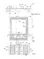
- FIG. 1illustrates a pixel 100 of an image sensor formed in a P-type substrate 102 .
- a photodiode of the pixelcomprises a heavily-doped P-type layer (P+) 104 formed over an N-type well 106 , formed in the P-type substrate.
- a transfer transistorcomprises a gate stack 108 formed on the surface of the P-substrate 102 on one side of the photodiode.
- a drain 110is formed of a heavily-doped N-type region, and is coupled to a sense node SN. Charges accumulated by the photodiode during an integration phase can be transferred to the sense node by applying a voltage signal to the gate electrode of the transfer transistor.
- the pixel 100is insulated from adjacent pixels on each side by shallow trench isolation (STI) regions 112 , 114 .
- a spacing 116can be provided between the STI 112 and the N-type well of the photodiode to provide electrical continuity between the surface P+ layer 104 and the P-type substrate 102 , and reduce the risk of dark current generation in the photodiode.
- N well 106To increase the sensitivity of the image sensor and/or reduce its size, it would be desirable to increase the surface area and depth of the N well 106 . However, there are problems in increasing the size of N well 106 without limiting the charge that is transferred and/or without increasing the overall size of the image sensor.
- an image sensorcomprising: a first pixel positioned between second and third pixels, each of the first, second and third pixels comprising a photodiode region surrounded by an isolation trench; a first charge transfer gate comprising a first column electrode surrounded by an insulating layer and positioned in an opening of the isolation trench between the first and second pixels, the first column electrode being configured to receive a first transfer voltage signal; and a second charge transfer gate comprising a second column electrode surrounded by an insulating layer and positioned in an opening of the isolation trench between the first and third pixels, the second column electrode being configured to receive a second transfer voltage signal.
- the image sensorfurther comprises: a first charge collection node associated with said first charge transfer gate for collecting charge stored in the photodiode regions of the first and second pixels; and a second charge collection node associated with said second charge transfer gate for collecting charge stored in the photodiode regions of the first and third pixels.
- At least a portion of the isolation trench of the first pixelis common to the first and second pixels.
- the opening between the first and second pixelsis formed in a common section of said isolation trench between the first and second pixels.
- the image sensorfurther comprises a control block configured to apply, during a read phase of the image sensor, the first transfer voltage signal to the first column electrode to transfer charge stored by said first and second pixels to said first charge collection node prior to applying said second transfer voltage signal to the second column electrode to transfer charge stored by said first and third pixels to said second charge collection node.
- the image sensorfurther comprises a further charge transfer gate comprising a further column electrode insulated from second photodiode region by an insulating layer and positioned in an opening between the second pixel and a charge collection region, the further column electrode being configured to receive a further transfer voltage.
- the photodiode regions of the first, second and third pixelscomprise a heavily doped P-type layer formed over an N-type region.
- the isolation trenches of the first, second and third pixelsare filled with a conductive material.
- the trenches of the first, second and third pixels and the first and second charge transfer gateshave a depth of between 1 and 10 ⁇ m.
- the first and second charge collection nodesare each coupled to a common sense node of pixel control circuitry arranged to read a voltage level associated with said first and second photodiode regions.
- the image sensorcomprises an array of said first, second and third pixels.
- an electronic image capturing devicecomprising the above image sensor.
- a method of manufacturing an image sensorcomprising an array of pixels, the method comprising: forming a first pixel between second and third pixels, each of the first, second and third pixels comprising a photodiode region surrounded by an isolation trench; forming a first charge transfer gate comprising a first column electrode surrounded by an insulating layer and positioned in an opening of the isolation trench between the first and second pixels, the first column electrode being configured to receive a first transfer voltage signal; and forming a second charge transfer gate comprising a second column electrode surrounded by an insulating layer and positioned in an opening of the isolation trench between the first and third pixels, the second column electrode being configured to receive a second transfer voltage signal.
- the methodfurther comprises forming a first charge collection node associated with said first charge transfer gate for collecting charge stored in the photodiode regions of the first and second pixels; and forming a second charge collection node associated with said second charge transfer gate for collecting charge stored in the photodiode regions of the first and third pixels.
- FIG. 1(described above) is a cross-section view of a pixel
- FIG. 2is a plan view of a pixel according to an embodiment
- FIGS. 3A and 3Bare cross-sections of the pixel of FIG. 2 ;
- FIG. 4is a plan view of a pixel according to an embodiment of the present invention.
- FIGS. 5A and 5Bare cross-sections of the pixel of FIG. 4 ;
- FIGS. 5C and 5Dare planar views of the pixel of FIG. 4 ;
- FIG. 6is a plan view of a portion of an image sensor according to an embodiment of the present invention.
- FIG. 7illustrates schematically a pixel circuit according to an embodiment of the present invention
- FIG. 8shows timing signals applied to the circuit of FIG. 7 according to an embodiment of the present invention
- FIG. 9illustrates schematically a portion of a pixel circuit according to an alternative embodiment of the present invention.
- FIG. 10illustrates an electronic device comprising an image sensor according to embodiments of the present invention.
- FIG. 2is a plan view of a pixel 200 that has been proposed by the present applicant in French patent application FR 08/52759 and in U.S. patent application Ser. No. 12/429,413, which are hereby incorporated by reference to the maximum extent allowable by the law.
- the pixel 200comprises a rectangular photodiode region 201 , which is, for example, around 1 ⁇ m square, surrounded by a rectangular trench 202 .
- Trench 202comprises an insulating layer 204 , and a conducting core 206 formed of a conducting material.
- a charge transfer gate 210is positioned approximately halfway across the opening 208 , and comprises a rectangular column, for example having the same thickness as the trench 202 .
- the column 210comprises a conductive core 212 forming a gate electrode surrounded by an insulating layer 214 forming a gate insulation.
- the opening 208leads to a charge collection region 216 , which is surrounded by a rectangular extension 218 of the trench 202 .
- FIG. 3Aillustrates the cross-section A-A of the pixel of FIG. 2 , passing through the side of the rectangular trench 202 with opening 208 and column 210 .
- the pixelis formed of an N-type layer 302 , for example between 1 and 8 ⁇ m in depth, positioned over a P-type substrate 304 .
- the trench 202for example, extends to the same depth as the column 210 , which is, for example, in the range 1 to 10 ⁇ m.
- the column 210 and/or trench 202for example, extend a short way into the P-type substrate.
- a heavily doped P-type (P+) layer 306is formed over the N-type layer 302 , forming an N-type well 308 .
- FIG. 3Billustrates the cross-section B-B of the pixel of FIG. 2 , which is perpendicular to cross-section A-A, and a passes through the opening 208 on one side of the column 210 .
- the N-type layer 302is continuous from the region 201 to the region 216 through the opening 208 , but within region 216 , a heavily doped N-type layer (N+) 310 is formed over the N-well 308 having, for example, a depth greater than that of the P+ layer 306 .
- P+ layer 306has a depth of around 0.1 ⁇ m and N+ layer 310 has a depth of around 0.3 ⁇ m.
- One drawback of the pixel of FIG. 2is that the charge collection region 216 does not form part of the photodiode region of the device, and thus limits the percentage of each pixel that can be used for charge collection and storage.
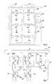
- FIG. 4illustrates a portion 400 of an image sensor comprising a pixel 401 , and portions of further pixels 402 and 403 positioned adjacently on opposite sides of pixel 401 .
- Pixel 401comprises a photodiode region 404 surrounded by a rectangular trench 406 , having openings 408 and 410 formed on opposite sides. Opening 408 is common to the trenches 406 and 413 , and leads from the photodiode region 404 to a photodiode region 412 of the adjacent pixel 402 .
- the photodiode region 412is also surrounded by a rectangular trench 413 , of which portions 414 and 415 on either side of opening 408 are common to the rectangular trench 406 .
- the rectangular trenches 406 and 413share a common side in which the opening 408 is formed.
- Opening 410is common to the trenches 406 and 417 , and leads from the photodiode region 404 to a photodiode region 416 of the adjacent pixel 403 .
- the photodiode region 416is also surrounded by a rectangular trench 417 , of which portions 418 and 419 on either side of opening 410 are common to the rectangular trench 406 .
- rectangular trenches 406 and 417share a common side in which the opening 410 is formed.
- the trenches 406 , 413 and 417are active DTIs (deep trench isolations) comprising an insulating layer 420 , and a conductive core 422 formed of a conducting material.
- the insulating layer 420electrically insulates the conducting core 422 from the surrounding silicon.
- the insulating layer 420is formed of silicon oxide, silicon nitride, silicon oxynitride, or a multi-layer structure comprising any combination of these materials, and has a thickness in the range 5 to 15 nm, for example around 7 nm.
- the conductive material 422is polysilicon having, for example a dopant concentration greater than 10 19 at./cm 3 .
- the trenches 406 , 413 and 417are, for example, between 0.1 and 0.5 ⁇ m in thickness, and between 1 and 10 ⁇ m in depth. In alternative embodiments, trenches 406 , 413 and 417 could be non-active DTIs, comprising only an insulating material, for example one of the insulating materials of layer 420 listed above.
- a respective column 424 , 425is formed having a width in the range 0.1 and 0.4 ⁇ m, for example around 0.3 ⁇ m, and a thickness approximately equal to that of trenches 406 , 413 , 417 .
- Columns 424 , 425are similar to column 210 of FIG. 2 , and form charge transfer gates having a conducting core 426 surrounded by and insulated from the silicon of the photodiode regions by an insulating layer 428 .
- the conducting core 426 and insulating layer 428are, for example, formed of the same materials as the conductive core 422 and insulating layer 420 of the trenches 406 , 413 , 417 , and form gate electrodes and gate insulations respectively of the charge transfer gates 424 , 425 .
- the openings 408 and 410have, for example, widths of between one quarter and three quarters of the length of the sides within which they are formed. For example, assuming that trenches 406 , 413 and 417 each form a rectangle around 1 ⁇ m square, the widths of openings 408 and 410 are, for example, between 0.25 and 0.75 ⁇ m, such as around 0.5 ⁇ m. Alternatively, the openings 408 , 410 could extend across the whole width, the portions 414 , 415 , 418 and 419 being removed. In this case, the width of columns 424 , 425 could be between 50 and 90 percent of the width of the openings 408 , 410 . The columns 424 , 425 could also have other shapes. For example, they could be formed to have the shape of a “T”, the shape of a “+”, or the shape of an “H”.
- charge collection nodes 430 and 432are formed of relatively small areas of heavily doped N-type (N+) material positioned within the openings 408 , 410 respectively, on one side of each of the columns 424 , 425 . These nodes effectively form drains of the transfer transistors implemented by the charge transfer gates 424 , 425 . For example, at least one side of the charge collection nodes 430 , 432 contacts the exterior surface of columns 424 , 425 respectively, to help provide a good passage for current flow between the photodiode regions and the charge collection nodes.
- N+N-type
- FIG. 5Ashows a cross-section C-C of the structure of FIG. 4 , passing along the boundary between the two pixels 401 and 402 , and passing through the column 424 .
- the structure shown by this cross-section C-Cis similar to the structure shown by cross-section A-A of pixel 200 , and comprises a layer 502 of N-type silicon formed by, for example, epitaxy, on a P-type substrate 504 .
- a heavily doped P-type layer 506is formed over the N-type layer 502 within the photodiode regions 404 , 412 and 416 .
- the N-type layer 502has, for example, a dopant concentration of between 10 15 at./cm 3 and 10 17 at./cm 3
- the P+ layer 506for example has a doping concentration greater than 10 18 at./cm 3 .
- the N+ region 430is shown formed over the N-type layer 502 in the gap between the column 424 and the trench portion 415 .
- the charge collection node 430contacts, for example, the insulating layers 420 , 428 on either side.
- the columns 424 and 425 and trenches 406 , 413 and 417extend through the whole depth of the N-type layer 502 and also, for example, extend between 0.1 and 2 ⁇ m into the substrate 504 .
- the trenches 406 , 413 , 417 and columns 424 , 425do not penetrate into the substrate 504 .
- FIG. 5Bshows a cross-section D-D of the structure of FIG. 4 , passing perpendicular to cross-section C-C, and traversing the two columns 424 and 425 .
- the N-type layer 502 formed over the P-type substrate 504is illustrated, along with the P+ layer 506 .
- FIGS. 5C and 5Dboth show a cross-section E-E of FIG. 5B traversing the N-type layer 502 , and thus providing horizontal planar views of the pixel N-wells.
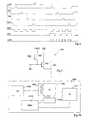
- a transfer voltage TGis applied to the conductive cores 426 of the columns 422 , 424 .
- a low biasing voltageis, for example, applied to the conductive core 422 of the trenches 406 , 413 and 417 .
- this polarizing voltagehas a constant low level during the integration phase and during the read phase at the end of the integration phase.
- TGis at a low voltage V L , for example between 0 and ⁇ 1 V. This results in an accumulation of holes around the columns.
- V Llow voltage
- Light penetrating the photodiode region 406 during the integration phaseresults in an accumulation of electrons in the N-type wells of the photodiodes. These electrons are effectively trapped, and will not move through the openings 408 , 410 to the adjacent N-wells due to the holes accumulated around the columns 424 , 425 .
- the accumulated chargesare transferred by applying a high voltage V H , for example of between 1 and 3 V, to the column 424 , while keeping the column 425 at the low voltage V L .
- V Hhigh voltage
- V Llow voltage
- FIG. 5BThis sequence is shown in FIG. 5B .
- transfer T 1electrons in the N-well of pixel 401 are conducted via a channel created by column 424 to the charge collection node 430 (not shown in FIG. 5B ).
- the charge of pixel 402is, for example, transferred first, such that when the transfer T 1 is performed via column 424 to empty pixel 401 , very little or no charge is transferred from the N-well of pixel 402 , as represented by the dashed arrow T 1 . Likewise, when a subsequent transfer is performed for pixel 403 , little or no charge is transferred from pixel 401 , as the N-well of pixel 401 has already been emptied.
- FIG. 6illustrates a portion 600 of an image sensor comprising a grid 602 of rectangular trenches surrounding photodiode regions of pixels formed in columns.
- Four pixelsare shown, two of which, 604 , 606 , are arranged in a column 607 , and another two of which, 608 , 610 , are arranged in an adjacent column 611 .
- adjacent pixelsshare charge transfer gates positioned in openings communicating between them.
- a charge transfer gate 612is positioned between pixels 604 and 606
- a charge transfer gate 614is positioned between pixels 608 and 610
- charge transfer gates 616 and 618are positioned between pixels 606 , 610 and the subsequent pixels of the respective columns (not illustrated in FIG. 6 ).
- the charge transfer gates 612 , 614 , 616 and 618are the same as gates 424 and 425 described above.
- Pixels 604 and 608are the first pixels of their respective columns, and a charge collection region 620 is formed adjacent to each of these pixels, similar to the charge collection region 216 of the pixel 200 of FIG. 2 .
- the regions 620communicate with the photodiode regions of pixels 604 , 608 via respective openings, in which charge transfer gates 622 , 624 are formed, each being similar to column 210 of FIG. 2 .
- the charge transfer gates 622 , 624 and corresponding charge collection regions 620allow only the charge present in pixels 604 and 608 to be transferred, these pixels being the first to be emptied at the start of a transfer phase of the image sensor.
- each columnhas no charge transfer gate, these final pixels only sharing a charge transfer gate with one adjacent pixel. While not illustrated in FIG. 6 , there may be hundreds or thousands of pixels in each column 607 , 611 . Furthermore, the image sensor may comprise hundreds or thousands of columns similar to columns 607 , 611 .
- a Bayer filteris for example positioned over the image sensor of FIG. 6 , part of which is represented by dashed line 626 .
- the pixels 604 and 610are, for example, associated with green filters, such that they capture green light, while the pixels 606 and 608 are, for example, associated with blue and red filters respectively, such that they capture blue and red light.
- the four pixels 604 to 610together form, for example, a particular pattern separating the colors of the image sensor.
- a reset transistor 628 , source follower transistor 630 and read transistor 632are formed in the image sensor adjacent to column 611 , and perform, for example, the function of reading voltages from pixels 604 , 606 , 608 and 610 , as will now be described with reference to FIG. 7 .
- FIG. 7illustrates schematically a pixel circuit 700 for reading the four pixels 604 to 610 of FIG. 6 .
- the circuit 700comprises photodiodes 704 , 706 , 708 and 710 corresponding to the photodiode regions of pixels 604 , 606 , 608 and 610 respectively of FIG. 6 .
- Each of the photodiodes 704 to 710has its anode coupled to ground, and its cathode coupled a sense node 712 via a pair of transistors implemented by the charge transfer gates between the pixels.
- a transistor 714corresponds to the charge transfer gate 622 of FIG. 6
- the gate node of transistor 714which corresponds to the conductive core of the charge transfer gate 622
- a pair of transistors 716corresponds to the charge transfer gate 612 of FIG. 6 , one of the pair coupling photodiode 704 to the sense node 712 , and the other coupling the photodiode 706 to the sense node 712 .
- the gate nodes of transistors 716receive the transfer voltage signal TG 1 from the control block 715 .
- a transistor 718corresponds to the charge transfer gate 624 of FIG. 6 , and the gate node of transistor 718 is coupled to the control block 715 for receiving a transfer voltage signal TG 2 .
- a pair of transistors 720corresponds to the charge transfer gate 614 of FIG. 6 , one of the pair coupling photodiode 708 to the sense node 712 , and the other coupling the photodiode 710 to the sense node 712 .
- the gate nodes of transistors 720receive the transfer voltage signal TG 3 from the control block 715 .
- transistors 722 , 724correspond to the charge transfer gates 616 , 618 of FIG. 6 respectively coupling a respective photodiode 706 , 710 to the sense node of a separate pixel circuit (not shown in FIG. 7 ). Transistors 722 , 724 are only activated once the charge from photodiodes 706 , 710 has been transferred to sense node 712 .
- the sense node 712is coupled to the gate node of the source follower transistor 630 , which has its source coupled to a read column line 726 via the read transistor 632 , and its drain node coupled to a voltage supply VRT.
- the gate node of the read transistor 632is coupled to receive a read voltage RD from the control circuitry 715 .
- the sense node 712is also coupled to the voltage supply VRT via the reset transistor 628 , which receives at its gate node a reset signal RST.
- circuit of FIG. 7applies to four pixels sharing a same sense node and arranged in a 2 by 2 block, such as the pixels 604 , 606 , 608 and 610 of FIG. 6
- the circuitcould be adapted to a 1 by 4 or a 4 by 1 arrangement of pixels sharing a common sense node arranged in a column or row.
- the transfer voltage signals TG 0 to TG 3are then brought low one after the other, thus isolating the corresponding photodiodes from the sense node 712 .
- the reset signalis also brought low.
- the transfer voltage TG 0is then brought high for a short period, and a second read is made of the sense node, to read a second reference voltage, and thus determine the charge offset occurring due to a read.
- the transfer gate voltage TG 0is then brought low again, starting integration period t i of the photodiode 704 .
- the transfer and read phase of the photodiodeis implemented as follows.
- the read signal RDis brought high, the reset signal RST is brought low, and the transfer voltage TG 0 is brought high for a short period, such that the charge is transferred from the photodiode 704 to the sense node SN.
- the signal CDScorrelated double sampling
- the levels before and after the charge is transferred to the sense nodeare stored in two sampling capacitors, and then a digital or analogue subtraction is applied to the stored signals in order to determine the signal without dispersions resulting from differences in the threshold voltage V t and in kTC noise, where k is Boltzmann's constant, T is temperature, and C is the capacitance.
- the voltage at the sense nodeis then reset by applying the reset signal RST, which is brought low again prior to reading the voltage at the photodiode 706 . The reading sequence continues in this fashion for the other photodiodes.
- the sequence shown in FIG. 8corresponds to the read sequence of one group of pixels coupled to a common sense node of a pixel circuit. This sequence is, for example, repeated for all of the pixel circuits of the image sensor in turn, operation being that of a rolling shutter.
- FIG. 7While the circuit of FIG. 7 is of a 1T75 type (four charge transfer gates and three other transistors, and four photodiodes), the pixels described herein could be used equally in other pixel circuit types, such as 1T5, 2T, 2T5 or 4T circuits. In the case of a 4T architecture, a single diode is connected to the sense node of a read system comprising three transistors such as the transistors 628 , 630 and 632 of FIG. 7 .
- FIG. 9illustrates read circuitry 900 of a pixel circuit corresponding, for example, to a 2T pixel circuit type.
- the sense node 901is, for example, coupled to two of the pixels as described above.
- sense node 901is coupled to a reset voltage VRST by a reset transistor 902 , and to the gate node of a sense transistor 904 , which is coupled between a further supply voltage VRT and a column read line 906 .
- the readis performed by applying the voltage VRST during a reset, and subsequently transferring a photodiode charge to the sense node 901 , which can then be read on line 906 .
- FIG. 10illustrates an electronic device 1000 , comprising a microprocessor 1002 , and an image sensor 1004 comprising, for example, an array of the pixels as described herein, and associated with a control circuit 1006 , which generates the signals RST, TG and RD for controlling the pixel circuits of the image sensor.
- Read circuitry 1008is also coupled to the image sensor, for example comprising switches and capacitors for sampling and storing voltage values read from the column read lines of the image sensor 1004 .
- a memory 1010for example stores images captured by the image sensor, and a display 1012 for example displays captured images.
- the electronic device 1000is, for example, a digital still and/or video camera, mobile device or portable games console having image capturing capabilities, a webcam, laptop computer or other digital image capturing device having an image sensor adapted to capture still images and/or video.
- An advantage of the embodiments described hereinis that the pixels have a high percentage of their area performing the function of a photodiode, and a relatively small percentage of their area performing the function of the transfer transistor.
- the image sensorcan have a greater sensitivity and/or occupy less chip area.
- the pixelscould be formed in rows, with charge transfer columns positioned between pixels of the same row.
- the charge transfer columnscould have shapes other than those described above, for example extending across the whole width of the pixel and even integrating a portion of the adjacent sides.
- each pixel circuitcould be coupled to a different group of pixels than the group shown in FIG. 6 .
- each pixelis surrounded by an active DTI
- the DTIcould be non-active, for example formed only of an insulating layer.
Landscapes
- Solid State Image Pick-Up Elements (AREA)
- Transforming Light Signals Into Electric Signals (AREA)
Abstract
Description
Claims (26)
Applications Claiming Priority (3)
| Application Number | Priority Date | Filing Date | Title |
|---|---|---|---|
| FR0957427 | 2009-10-22 | ||
| FR09/57427 | 2009-10-22 | ||
| FR0957427 | 2009-10-22 |
Publications (2)
| Publication Number | Publication Date |
|---|---|
| US20110096208A1 US20110096208A1 (en) | 2011-04-28 |
| US8531567B2true US8531567B2 (en) | 2013-09-10 |
Family
ID=42163722
Family Applications (1)
| Application Number | Title | Priority Date | Filing Date |
|---|---|---|---|
| US12/910,176Active2031-07-20US8531567B2 (en) | 2009-10-22 | 2010-10-22 | Image sensor with vertical transfer gate |
Country Status (2)
| Country | Link |
|---|---|
| US (1) | US8531567B2 (en) |
| EP (1) | EP2315251A1 (en) |
Cited By (17)
| Publication number | Priority date | Publication date | Assignee | Title |
|---|---|---|---|---|
| US20110134298A1 (en)* | 2008-08-11 | 2011-06-09 | Honda Motor Co., Ltd. | Pixel, pixel forming method, imaging device and imaging forming method |
| US20130321685A1 (en)* | 2012-05-31 | 2013-12-05 | Samsung Electronics Co., Ltd. | Unit pixel of image sensor and pixel array including the unit pixel |
| US20140146197A1 (en)* | 2012-11-29 | 2014-05-29 | Canon Kabushiki Kaisha | Image pickup element, image pickup apparatus, and image pickup system |
| US8773562B1 (en) | 2013-01-31 | 2014-07-08 | Apple Inc. | Vertically stacked image sensor |
| US20150155327A1 (en)* | 2013-11-29 | 2015-06-04 | Sony Corporation | Solid-state imaging element, manufacturing method, and electronic device |
| US9245974B2 (en) | 2014-02-24 | 2016-01-26 | Taiwan Semiconductor Manufacturing Co., Ltd. | Performance boost by silicon epitaxy |
| US20160079465A1 (en)* | 2011-12-21 | 2016-03-17 | Infineon Technologies Ag | Photo cell devices for phase-sensitive detection of light signals |
| US9385157B2 (en) | 2014-07-11 | 2016-07-05 | Samsung Electronics Co., Ltd. | Pixel of an image sensor, and image sensor |
| US20170207270A1 (en)* | 2016-01-15 | 2017-07-20 | Semiconductor Manufacturing International (Shanghai) Corporation | Method of manufacturing a cmos image sensor |
| US20170294468A1 (en)* | 2016-04-08 | 2017-10-12 | SK Hynix Inc. | Image sensor and method for fabricating the same |
| US10128292B2 (en) | 2016-12-13 | 2018-11-13 | Stmicroelectronics (Research & Development) Limited | Charge storage cell and method of manufacturing a charge storage cell |
| US10163963B2 (en) | 2017-04-05 | 2018-12-25 | Semiconductor Components Industries, Llc | Image sensors with vertically stacked photodiodes and vertical transfer gates |
| US10475848B2 (en) | 2017-12-12 | 2019-11-12 | Stmicroelectronics (Crolles 2) Sas | Integrated circuit image sensor cell with skimming gate implemented using a vertical gate transistor structure |
| US10971533B2 (en) | 2018-01-29 | 2021-04-06 | Stmicroelectronics (Crolles 2) Sas | Vertical transfer gate with charge transfer and charge storage capabilities |
| FR3124311A1 (en)* | 2021-06-16 | 2022-12-23 | Stmicroelectronics (Crolles 2) Sas | Photosensitive sensor and corresponding method of manufacture. |
| US11736826B2 (en) | 2019-06-28 | 2023-08-22 | Stmicroelectronics (Crolles 2) Sas | Pixel and method for controlling the same |
| US12185018B2 (en) | 2019-06-28 | 2024-12-31 | Apple Inc. | Stacked electromagnetic radiation sensors for visible image sensing and infrared depth sensing, or for visible image sensing and infrared image sensing |
Families Citing this family (22)
| Publication number | Priority date | Publication date | Assignee | Title |
|---|---|---|---|---|
| US20100044676A1 (en) | 2008-04-18 | 2010-02-25 | Invisage Technologies, Inc. | Photodetectors and Photovoltaics Based on Semiconductor Nanocrystals |
| WO2011156507A1 (en) | 2010-06-08 | 2011-12-15 | Edward Hartley Sargent | Stable, sensitive photodetectors and image sensors including circuits, processes, and materials for enhanced imaging performance |
| FR2980641B1 (en)* | 2011-09-28 | 2014-04-11 | E2V Semiconductors | VERTICAL GRID ELECTRON MULTIPLICATION IMAGE SENSOR |
| FR2983347B1 (en)* | 2011-11-28 | 2014-07-25 | Commissariat Energie Atomique | DIODE ARRAY DEVICE HAVING ACCESS RESISTORS AND IMPROVED STABILITY |
| FR2984607A1 (en)* | 2011-12-16 | 2013-06-21 | St Microelectronics Crolles 2 | CURED PHOTODIODE IMAGE SENSOR |
| FR3000606B1 (en)* | 2013-01-02 | 2015-01-30 | Commissariat Energie Atomique | IMAGE SENSOR |
| KR102087233B1 (en) | 2013-01-17 | 2020-03-10 | 삼성전자주식회사 | Semiconductor cmos image sensor(cis) having vertical transfer gate (vtg) and a method for production thereof |
| JP2015053411A (en) | 2013-09-09 | 2015-03-19 | ソニー株式会社 | Solid-state imaging device, method for manufacturing solid-state imaging device, and electronic equipment |
| FR3019379A1 (en)* | 2014-03-31 | 2015-10-02 | St Microelectronics Crolles 2 | VERTICAL GRID TRANSISTOR AND PIXEL STRUCTURE COMPRISING SUCH A TRANSISTOR |
| FR3021807B1 (en) | 2014-05-27 | 2017-09-29 | Commissariat A L Energie Atomique Et Aux Energies Alternatives | IMPROVED FTM MESA PHOTODIOD MATRIX MATRIX |
| US9941316B2 (en) | 2014-06-10 | 2018-04-10 | Invisage Technologies, Inc. | Multi-terminal optoelectronic devices for light detection |
| US9406718B2 (en)* | 2014-09-29 | 2016-08-02 | Omnivision Technologies, Inc. | Image sensor pixel cell with non-destructive readout |
| FR3027732B1 (en)* | 2014-10-27 | 2016-12-23 | Commissariat Energie Atomique | VERTICAL ELECTRODES IMAGE SENSOR |
| KR102456530B1 (en) | 2015-09-09 | 2022-10-20 | 삼성전자주식회사 | Image sensor |
| FR3043250A1 (en) | 2015-10-30 | 2017-05-05 | St Microelectronics Crolles 2 Sas | IMAGE SENSOR |
| FR3049389A1 (en)* | 2016-03-22 | 2017-09-29 | St Microelectronics Crolles 2 Sas | INSULATION WALL AND METHOD OF MANUFACTURE |
| US10872918B2 (en)* | 2017-03-28 | 2020-12-22 | Taiwan Semiconductor Manufacturing Co., Ltd. | Optical isolation structure for reducing crosstalk between pixels and fabrication method thereof |
| JP7250427B2 (en) | 2018-02-09 | 2023-04-03 | キヤノン株式会社 | PHOTOELECTRIC CONVERSION DEVICE, IMAGING SYSTEM AND MOVING OBJECT |
| US10741592B2 (en) | 2018-06-07 | 2020-08-11 | Semiconductor Components Industries, Llc | Image sensors with multi-photodiode image pixels and vertical transfer gates |
| FR3094571B1 (en)* | 2019-03-27 | 2022-04-29 | St Microelectronics Crolles 2 Sas | Photodiode electronic device |
| FR3098988B1 (en) | 2019-07-19 | 2022-08-26 | St Microelectronics Crolles 2 Sas | Image sensor |
| FR3134236A1 (en)* | 2022-04-01 | 2023-10-06 | Stmicroelectronics (Crolles 2) Sas | Photodiode and method of manufacturing a photodiode |
Citations (13)
| Publication number | Priority date | Publication date | Assignee | Title |
|---|---|---|---|---|
| US4477835A (en)* | 1981-03-13 | 1984-10-16 | Thomson-Csf | Charge transfer photosensitive device |
| US6545302B2 (en)* | 2000-08-31 | 2003-04-08 | Hyundai Electronics Industries Co., Ltd. | Image sensor capable of decreasing leakage current between diodes and method for fabricating the same |
| US6657665B1 (en)* | 1998-12-31 | 2003-12-02 | Eastman Kodak Company | Active Pixel Sensor with wired floating diffusions and shared amplifier |
| US20060081887A1 (en) | 2004-10-20 | 2006-04-20 | Samsung Electronics Co., Ltd. | Solid state image sensor devices having non-planar transistors |
| US20060124976A1 (en) | 2004-12-15 | 2006-06-15 | International Business Machines Corporation | Recessed gate for an image sensor |
| US20060256221A1 (en) | 2005-05-11 | 2006-11-16 | Micron Technology, Inc. | High fill factor multi-way shared pixel |
| US20060274176A1 (en) | 2005-06-01 | 2006-12-07 | Eastman Kodak Company | CMOS image sensor pixel with selectable binning and conversion gain |
| US20080303930A1 (en)* | 2007-04-16 | 2008-12-11 | Canon Kabushiki Kaisha | Photoelectric conversion device and image-pickup apparatus |
| US7492027B2 (en)* | 2004-02-20 | 2009-02-17 | Micron Technology, Inc. | Reduced crosstalk sensor and method of formation |
| US20090266973A1 (en) | 2008-04-24 | 2009-10-29 | Stmicroelectronics Crolles 2 Sas | Very small image sensor |
| US20090303371A1 (en) | 2008-06-09 | 2009-12-10 | Sony Corporation | Solid-state imaging device, drive method thereof and electronic apparatus |
| US20110089311A1 (en)* | 2009-10-20 | 2011-04-21 | Omnivision Technologies, Inc. | Trench transfer gate for increased pixel fill factor |
| US8310003B2 (en)* | 2008-07-31 | 2012-11-13 | Kabushiki Kaisha Toshiba | Solid-state imaging device with vertical gate electrode and method of manufacturing the same |
Family Cites Families (1)
| Publication number | Priority date | Publication date | Assignee | Title |
|---|---|---|---|---|
| FR852759A (en) | 1940-03-06 |
- 2010
- 2010-10-22EPEP10188591Apatent/EP2315251A1/ennot_activeWithdrawn
- 2010-10-22USUS12/910,176patent/US8531567B2/enactiveActive
Patent Citations (14)
| Publication number | Priority date | Publication date | Assignee | Title |
|---|---|---|---|---|
| US4477835A (en)* | 1981-03-13 | 1984-10-16 | Thomson-Csf | Charge transfer photosensitive device |
| US6657665B1 (en)* | 1998-12-31 | 2003-12-02 | Eastman Kodak Company | Active Pixel Sensor with wired floating diffusions and shared amplifier |
| US6545302B2 (en)* | 2000-08-31 | 2003-04-08 | Hyundai Electronics Industries Co., Ltd. | Image sensor capable of decreasing leakage current between diodes and method for fabricating the same |
| US7492027B2 (en)* | 2004-02-20 | 2009-02-17 | Micron Technology, Inc. | Reduced crosstalk sensor and method of formation |
| US20060081887A1 (en) | 2004-10-20 | 2006-04-20 | Samsung Electronics Co., Ltd. | Solid state image sensor devices having non-planar transistors |
| US20070184614A1 (en)* | 2004-12-15 | 2007-08-09 | International Business Machines Corporation | Recessed gate for a cmos image sensor |
| US20060124976A1 (en) | 2004-12-15 | 2006-06-15 | International Business Machines Corporation | Recessed gate for an image sensor |
| US20060256221A1 (en) | 2005-05-11 | 2006-11-16 | Micron Technology, Inc. | High fill factor multi-way shared pixel |
| US20060274176A1 (en) | 2005-06-01 | 2006-12-07 | Eastman Kodak Company | CMOS image sensor pixel with selectable binning and conversion gain |
| US20080303930A1 (en)* | 2007-04-16 | 2008-12-11 | Canon Kabushiki Kaisha | Photoelectric conversion device and image-pickup apparatus |
| US20090266973A1 (en) | 2008-04-24 | 2009-10-29 | Stmicroelectronics Crolles 2 Sas | Very small image sensor |
| US20090303371A1 (en) | 2008-06-09 | 2009-12-10 | Sony Corporation | Solid-state imaging device, drive method thereof and electronic apparatus |
| US8310003B2 (en)* | 2008-07-31 | 2012-11-13 | Kabushiki Kaisha Toshiba | Solid-state imaging device with vertical gate electrode and method of manufacturing the same |
| US20110089311A1 (en)* | 2009-10-20 | 2011-04-21 | Omnivision Technologies, Inc. | Trench transfer gate for increased pixel fill factor |
Non-Patent Citations (1)
| Title |
|---|
| French Search Report from corresponding French Application No. 09/57427. |
Cited By (34)
| Publication number | Priority date | Publication date | Assignee | Title |
|---|---|---|---|---|
| US20110134298A1 (en)* | 2008-08-11 | 2011-06-09 | Honda Motor Co., Ltd. | Pixel, pixel forming method, imaging device and imaging forming method |
| US8860861B2 (en)* | 2008-08-11 | 2014-10-14 | Honda Motor Co., Ltd. | Pixel, pixel forming method, imaging device and imaging forming method |
| US20160079465A1 (en)* | 2011-12-21 | 2016-03-17 | Infineon Technologies Ag | Photo cell devices for phase-sensitive detection of light signals |
| US10483426B2 (en)* | 2011-12-21 | 2019-11-19 | Infineon Technologies Ag | Photo cell devices for phase-sensitive detection of light signals |
| US9025063B2 (en)* | 2012-05-31 | 2015-05-05 | Samsung Electronics Co., Ltd. | Unit pixel of image sensor and pixel array including the unit pixel |
| US20130321685A1 (en)* | 2012-05-31 | 2013-12-05 | Samsung Electronics Co., Ltd. | Unit pixel of image sensor and pixel array including the unit pixel |
| US20140146197A1 (en)* | 2012-11-29 | 2014-05-29 | Canon Kabushiki Kaisha | Image pickup element, image pickup apparatus, and image pickup system |
| US9450006B2 (en)* | 2012-11-29 | 2016-09-20 | Canon Kabushiki Kaisha | Image pickup element, image pickup apparatus, and image pickup system |
| US9224776B2 (en)* | 2012-11-29 | 2015-12-29 | Canon Kabushiki Kaisha | Image pickup element, image pickup apparatus, and image pickup system |
| US9245917B2 (en) | 2013-01-31 | 2016-01-26 | Apple Inc. | Vertically stacked image sensor |
| US10003759B2 (en) | 2013-01-31 | 2018-06-19 | Apple Inc. | Vertically stacked image sensor |
| US20160043126A1 (en)* | 2013-01-31 | 2016-02-11 | Apple Inc. | Vertically stacked image sensor |
| US9406713B2 (en)* | 2013-01-31 | 2016-08-02 | Apple Inc. | Vertically stacked image sensor |
| US8773562B1 (en) | 2013-01-31 | 2014-07-08 | Apple Inc. | Vertically stacked image sensor |
| US10462402B2 (en) | 2013-01-31 | 2019-10-29 | Apple Inc. | Image sensor having full well capacity beyond photodiode capacity |
| US20150155327A1 (en)* | 2013-11-29 | 2015-06-04 | Sony Corporation | Solid-state imaging element, manufacturing method, and electronic device |
| US9437636B2 (en)* | 2013-11-29 | 2016-09-06 | Sony Corporation | Solid-state imaging element, manufacturing method, and electronic device |
| US9245974B2 (en) | 2014-02-24 | 2016-01-26 | Taiwan Semiconductor Manufacturing Co., Ltd. | Performance boost by silicon epitaxy |
| US9595589B2 (en) | 2014-02-24 | 2017-03-14 | Taiwan Semiconductor Manufacturing Co., Ltd. | Transistor with performance boost by epitaxial layer |
| US9385157B2 (en) | 2014-07-11 | 2016-07-05 | Samsung Electronics Co., Ltd. | Pixel of an image sensor, and image sensor |
| US20170207270A1 (en)* | 2016-01-15 | 2017-07-20 | Semiconductor Manufacturing International (Shanghai) Corporation | Method of manufacturing a cmos image sensor |
| US10784303B2 (en)* | 2016-01-15 | 2020-09-22 | Semiconductor Manufacturing International (Shanghai) Corporation | Method of manufacturing a CMOS image sensor |
| US10008526B2 (en)* | 2016-04-08 | 2018-06-26 | SK Hynix Inc. | Image sensor and method for fabricating the same |
| US20170294468A1 (en)* | 2016-04-08 | 2017-10-12 | SK Hynix Inc. | Image sensor and method for fabricating the same |
| US10128292B2 (en) | 2016-12-13 | 2018-11-13 | Stmicroelectronics (Research & Development) Limited | Charge storage cell and method of manufacturing a charge storage cell |
| US10347680B2 (en) | 2016-12-13 | 2019-07-09 | Stmicroelectronics (Research & Development) Limited | Charge storage cell and method of manufacturing a charge storage cell |
| US10163963B2 (en) | 2017-04-05 | 2018-12-25 | Semiconductor Components Industries, Llc | Image sensors with vertically stacked photodiodes and vertical transfer gates |
| US10615217B2 (en) | 2017-04-05 | 2020-04-07 | Semiconductor Components Industries, Llc | Image sensors with vertically stacked photodiodes and vertical transfer gates |
| US11114493B2 (en) | 2017-04-05 | 2021-09-07 | Semiconductor Components Industries, Llc | Image sensors with vertically stacked photodiodes and vertical transfer gates |
| US10475848B2 (en) | 2017-12-12 | 2019-11-12 | Stmicroelectronics (Crolles 2) Sas | Integrated circuit image sensor cell with skimming gate implemented using a vertical gate transistor structure |
| US10971533B2 (en) | 2018-01-29 | 2021-04-06 | Stmicroelectronics (Crolles 2) Sas | Vertical transfer gate with charge transfer and charge storage capabilities |
| US11736826B2 (en) | 2019-06-28 | 2023-08-22 | Stmicroelectronics (Crolles 2) Sas | Pixel and method for controlling the same |
| US12185018B2 (en) | 2019-06-28 | 2024-12-31 | Apple Inc. | Stacked electromagnetic radiation sensors for visible image sensing and infrared depth sensing, or for visible image sensing and infrared image sensing |
| FR3124311A1 (en)* | 2021-06-16 | 2022-12-23 | Stmicroelectronics (Crolles 2) Sas | Photosensitive sensor and corresponding method of manufacture. |
Also Published As
| Publication number | Publication date |
|---|---|
| US20110096208A1 (en) | 2011-04-28 |
| EP2315251A1 (en) | 2011-04-27 |
Similar Documents
| Publication | Publication Date | Title |
|---|---|---|
| US8531567B2 (en) | Image sensor with vertical transfer gate | |
| US9024240B2 (en) | Compact image sensor arrangement with read circuitry over pixel zones | |
| KR101968197B1 (en) | Image sensor and method of forming the same | |
| JP4224036B2 (en) | Image sensor with embedded photodiode region and method of manufacturing the same | |
| JP6084922B2 (en) | Solid-state imaging device | |
| US9443892B2 (en) | Image sensor and method of forming the same | |
| US7235826B2 (en) | Solid-state image pickup device | |
| CN101609837B (en) | Solid-state imaging device, drive method thereof and electronic apparatus | |
| US7491990B2 (en) | CMOS image sensors for preventing optical crosstalk | |
| US9659987B2 (en) | Approach for reducing pixel pitch using vertical transfer gates and implant isolation regions | |
| US20090201400A1 (en) | Backside illuminated image sensor with global shutter and storage capacitor | |
| US20180337205A1 (en) | Solid-state image pickup device | |
| CN101211956A (en) | CMOS image sensor and manufacturing method thereof | |
| KR20160045054A (en) | Solid-state imaging element and electronic device | |
| CN102856334A (en) | Solid-state imaging apparatus, method of manufacturing solid-state imaging apparatus, and electronic apparatus | |
| US12224302B2 (en) | Image sensor pixels having reduced pitch | |
| US20210144319A1 (en) | Systems and methods for generating high dynamic range images | |
| JP6008669B2 (en) | Solid-state imaging device, manufacturing method thereof, and camera | |
| JP2016025331A (en) | Imaging device and method of manufacturing imaging device | |
| US9741758B2 (en) | Methods of forming image sensors including deposited negative fixed charge layers on photoelectric conversion regions | |
| KR102354801B1 (en) | Mos capacitor and image sensor having the same | |
| JP4857773B2 (en) | Solid-state imaging device and manufacturing method thereof | |
| JP2007115787A (en) | Solid-state image sensor | |
| JP2008198976A (en) | Solid-state imaging device and manufacturing method thereof | |
| HK1183162B (en) | Method, apparatus and system for providing improved full well capacity in an image sensor pixel |
Legal Events
| Date | Code | Title | Description |
|---|---|---|---|
| AS | Assignment | Owner name:STMICROELECTRONICS (CROLLES 2) SAS, FRANCE Free format text:ASSIGNMENT OF ASSIGNORS INTEREST;ASSIGNORS:ROY, FRANCOIS;BARBIER, FREDERIC;REEL/FRAME:025473/0761 Effective date:20101119 | |
| STCF | Information on status: patent grant | Free format text:PATENTED CASE | |
| AS | Assignment | Owner name:STMICROELECTRONICS SA, FRANCE Free format text:ASSIGNMENT OF ASSIGNORS INTEREST;ASSIGNOR:BARBIER, FREDERIC;REEL/FRAME:035681/0521 Effective date:20150511 Owner name:STMICROELECTRONICS SA, FRANCE Free format text:QUITCLAIM ASSIGNMENT;ASSIGNOR:STMICROELECTRONICS (CROLLES 2) SAS;REEL/FRAME:035743/0267 Effective date:20150513 | |
| FPAY | Fee payment | Year of fee payment:4 | |
| MAFP | Maintenance fee payment | Free format text:PAYMENT OF MAINTENANCE FEE, 8TH YEAR, LARGE ENTITY (ORIGINAL EVENT CODE: M1552); ENTITY STATUS OF PATENT OWNER: LARGE ENTITY Year of fee payment:8 | |
| AS | Assignment | Owner name:STMICROELECTRONICS FRANCE, FRANCE Free format text:CHANGE OF NAME;ASSIGNOR:STMICROELECTRONICS SA;REEL/FRAME:066357/0693 Effective date:20230126 | |
| MAFP | Maintenance fee payment | Free format text:PAYMENT OF MAINTENANCE FEE, 12TH YEAR, LARGE ENTITY (ORIGINAL EVENT CODE: M1553); ENTITY STATUS OF PATENT OWNER: LARGE ENTITY Year of fee payment:12 |