US8531359B2 - Pixel circuits and methods for driving pixels - Google Patents
Pixel circuits and methods for driving pixelsDownload PDFInfo
- Publication number
- US8531359B2 US8531359B2US12/692,453US69245310AUS8531359B2US 8531359 B2US8531359 B2US 8531359B2US 69245310 AUS69245310 AUS 69245310AUS 8531359 B2US8531359 B2US 8531359B2
- Authority
- US
- United States
- Prior art keywords
- current
- transistor
- storage node
- voltage
- period
- Prior art date
- Legal status (The legal status is an assumption and is not a legal conclusion. Google has not performed a legal analysis and makes no representation as to the accuracy of the status listed.)
- Active, expires
Links
Images


Classifications
- G—PHYSICS
- G09—EDUCATION; CRYPTOGRAPHY; DISPLAY; ADVERTISING; SEALS
- G09G—ARRANGEMENTS OR CIRCUITS FOR CONTROL OF INDICATING DEVICES USING STATIC MEANS TO PRESENT VARIABLE INFORMATION
- G09G3/00—Control arrangements or circuits, of interest only in connection with visual indicators other than cathode-ray tubes
- G09G3/20—Control arrangements or circuits, of interest only in connection with visual indicators other than cathode-ray tubes for presentation of an assembly of a number of characters, e.g. a page, by composing the assembly by combination of individual elements arranged in a matrix no fixed position being assigned to or needed to be assigned to the individual characters or partial characters
- G09G3/22—Control arrangements or circuits, of interest only in connection with visual indicators other than cathode-ray tubes for presentation of an assembly of a number of characters, e.g. a page, by composing the assembly by combination of individual elements arranged in a matrix no fixed position being assigned to or needed to be assigned to the individual characters or partial characters using controlled light sources
- G09G3/30—Control arrangements or circuits, of interest only in connection with visual indicators other than cathode-ray tubes for presentation of an assembly of a number of characters, e.g. a page, by composing the assembly by combination of individual elements arranged in a matrix no fixed position being assigned to or needed to be assigned to the individual characters or partial characters using controlled light sources using electroluminescent panels
- G09G3/32—Control arrangements or circuits, of interest only in connection with visual indicators other than cathode-ray tubes for presentation of an assembly of a number of characters, e.g. a page, by composing the assembly by combination of individual elements arranged in a matrix no fixed position being assigned to or needed to be assigned to the individual characters or partial characters using controlled light sources using electroluminescent panels semiconductive, e.g. using light-emitting diodes [LED]
- G09G3/3208—Control arrangements or circuits, of interest only in connection with visual indicators other than cathode-ray tubes for presentation of an assembly of a number of characters, e.g. a page, by composing the assembly by combination of individual elements arranged in a matrix no fixed position being assigned to or needed to be assigned to the individual characters or partial characters using controlled light sources using electroluminescent panels semiconductive, e.g. using light-emitting diodes [LED] organic, e.g. using organic light-emitting diodes [OLED]
- G09G3/3225—Control arrangements or circuits, of interest only in connection with visual indicators other than cathode-ray tubes for presentation of an assembly of a number of characters, e.g. a page, by composing the assembly by combination of individual elements arranged in a matrix no fixed position being assigned to or needed to be assigned to the individual characters or partial characters using controlled light sources using electroluminescent panels semiconductive, e.g. using light-emitting diodes [LED] organic, e.g. using organic light-emitting diodes [OLED] using an active matrix
- G09G3/3233—Control arrangements or circuits, of interest only in connection with visual indicators other than cathode-ray tubes for presentation of an assembly of a number of characters, e.g. a page, by composing the assembly by combination of individual elements arranged in a matrix no fixed position being assigned to or needed to be assigned to the individual characters or partial characters using controlled light sources using electroluminescent panels semiconductive, e.g. using light-emitting diodes [LED] organic, e.g. using organic light-emitting diodes [OLED] using an active matrix with pixel circuitry controlling the current through the light-emitting element
- G09G3/3241—Control arrangements or circuits, of interest only in connection with visual indicators other than cathode-ray tubes for presentation of an assembly of a number of characters, e.g. a page, by composing the assembly by combination of individual elements arranged in a matrix no fixed position being assigned to or needed to be assigned to the individual characters or partial characters using controlled light sources using electroluminescent panels semiconductive, e.g. using light-emitting diodes [LED] organic, e.g. using organic light-emitting diodes [OLED] using an active matrix with pixel circuitry controlling the current through the light-emitting element the current through the light-emitting element being set using a data current provided by the data driver, e.g. by using a two-transistor current mirror
- G09G3/325—Control arrangements or circuits, of interest only in connection with visual indicators other than cathode-ray tubes for presentation of an assembly of a number of characters, e.g. a page, by composing the assembly by combination of individual elements arranged in a matrix no fixed position being assigned to or needed to be assigned to the individual characters or partial characters using controlled light sources using electroluminescent panels semiconductive, e.g. using light-emitting diodes [LED] organic, e.g. using organic light-emitting diodes [OLED] using an active matrix with pixel circuitry controlling the current through the light-emitting element the current through the light-emitting element being set using a data current provided by the data driver, e.g. by using a two-transistor current mirror the data current flowing through the driving transistor during a setting phase, e.g. by using a switch for connecting the driving transistor to the data driver
- G—PHYSICS
- G09—EDUCATION; CRYPTOGRAPHY; DISPLAY; ADVERTISING; SEALS
- G09G—ARRANGEMENTS OR CIRCUITS FOR CONTROL OF INDICATING DEVICES USING STATIC MEANS TO PRESENT VARIABLE INFORMATION
- G09G3/00—Control arrangements or circuits, of interest only in connection with visual indicators other than cathode-ray tubes
- G09G3/20—Control arrangements or circuits, of interest only in connection with visual indicators other than cathode-ray tubes for presentation of an assembly of a number of characters, e.g. a page, by composing the assembly by combination of individual elements arranged in a matrix no fixed position being assigned to or needed to be assigned to the individual characters or partial characters
- G09G3/22—Control arrangements or circuits, of interest only in connection with visual indicators other than cathode-ray tubes for presentation of an assembly of a number of characters, e.g. a page, by composing the assembly by combination of individual elements arranged in a matrix no fixed position being assigned to or needed to be assigned to the individual characters or partial characters using controlled light sources
- G09G3/30—Control arrangements or circuits, of interest only in connection with visual indicators other than cathode-ray tubes for presentation of an assembly of a number of characters, e.g. a page, by composing the assembly by combination of individual elements arranged in a matrix no fixed position being assigned to or needed to be assigned to the individual characters or partial characters using controlled light sources using electroluminescent panels
- G09G3/32—Control arrangements or circuits, of interest only in connection with visual indicators other than cathode-ray tubes for presentation of an assembly of a number of characters, e.g. a page, by composing the assembly by combination of individual elements arranged in a matrix no fixed position being assigned to or needed to be assigned to the individual characters or partial characters using controlled light sources using electroluminescent panels semiconductive, e.g. using light-emitting diodes [LED]
- G09G3/3208—Control arrangements or circuits, of interest only in connection with visual indicators other than cathode-ray tubes for presentation of an assembly of a number of characters, e.g. a page, by composing the assembly by combination of individual elements arranged in a matrix no fixed position being assigned to or needed to be assigned to the individual characters or partial characters using controlled light sources using electroluminescent panels semiconductive, e.g. using light-emitting diodes [LED] organic, e.g. using organic light-emitting diodes [OLED]
- G09G3/3275—Details of drivers for data electrodes
- G09G3/3283—Details of drivers for data electrodes in which the data driver supplies a variable data current for setting the current through, or the voltage across, the light-emitting elements
- G—PHYSICS
- G09—EDUCATION; CRYPTOGRAPHY; DISPLAY; ADVERTISING; SEALS
- G09G—ARRANGEMENTS OR CIRCUITS FOR CONTROL OF INDICATING DEVICES USING STATIC MEANS TO PRESENT VARIABLE INFORMATION
- G09G2300/00—Aspects of the constitution of display devices
- G09G2300/08—Active matrix structure, i.e. with use of active elements, inclusive of non-linear two terminal elements, in the pixels together with light emitting or modulating elements
- G09G2300/0809—Several active elements per pixel in active matrix panels
- G09G2300/0819—Several active elements per pixel in active matrix panels used for counteracting undesired variations, e.g. feedback or autozeroing
- G—PHYSICS
- G09—EDUCATION; CRYPTOGRAPHY; DISPLAY; ADVERTISING; SEALS
- G09G—ARRANGEMENTS OR CIRCUITS FOR CONTROL OF INDICATING DEVICES USING STATIC MEANS TO PRESENT VARIABLE INFORMATION
- G09G2300/00—Aspects of the constitution of display devices
- G09G2300/08—Active matrix structure, i.e. with use of active elements, inclusive of non-linear two terminal elements, in the pixels together with light emitting or modulating elements
- G09G2300/0809—Several active elements per pixel in active matrix panels
- G09G2300/0842—Several active elements per pixel in active matrix panels forming a memory circuit, e.g. a dynamic memory with one capacitor
- G09G2300/0852—Several active elements per pixel in active matrix panels forming a memory circuit, e.g. a dynamic memory with one capacitor being a dynamic memory with more than one capacitor
- G—PHYSICS
- G09—EDUCATION; CRYPTOGRAPHY; DISPLAY; ADVERTISING; SEALS
- G09G—ARRANGEMENTS OR CIRCUITS FOR CONTROL OF INDICATING DEVICES USING STATIC MEANS TO PRESENT VARIABLE INFORMATION
- G09G2310/00—Command of the display device
- G09G2310/02—Addressing, scanning or driving the display screen or processing steps related thereto
- G09G2310/0243—Details of the generation of driving signals
- G09G2310/0248—Precharge or discharge of column electrodes before or after applying exact column voltages
- G—PHYSICS
- G09—EDUCATION; CRYPTOGRAPHY; DISPLAY; ADVERTISING; SEALS
- G09G—ARRANGEMENTS OR CIRCUITS FOR CONTROL OF INDICATING DEVICES USING STATIC MEANS TO PRESENT VARIABLE INFORMATION
- G09G2310/00—Command of the display device
- G09G2310/02—Addressing, scanning or driving the display screen or processing steps related thereto
- G09G2310/0264—Details of driving circuits
- G09G2310/027—Details of drivers for data electrodes, the drivers handling digital grey scale data, e.g. use of D/A converters
- G—PHYSICS
- G09—EDUCATION; CRYPTOGRAPHY; DISPLAY; ADVERTISING; SEALS
- G09G—ARRANGEMENTS OR CIRCUITS FOR CONTROL OF INDICATING DEVICES USING STATIC MEANS TO PRESENT VARIABLE INFORMATION
- G09G3/00—Control arrangements or circuits, of interest only in connection with visual indicators other than cathode-ray tubes
- G09G3/20—Control arrangements or circuits, of interest only in connection with visual indicators other than cathode-ray tubes for presentation of an assembly of a number of characters, e.g. a page, by composing the assembly by combination of individual elements arranged in a matrix no fixed position being assigned to or needed to be assigned to the individual characters or partial characters
- G09G3/22—Control arrangements or circuits, of interest only in connection with visual indicators other than cathode-ray tubes for presentation of an assembly of a number of characters, e.g. a page, by composing the assembly by combination of individual elements arranged in a matrix no fixed position being assigned to or needed to be assigned to the individual characters or partial characters using controlled light sources
- G09G3/30—Control arrangements or circuits, of interest only in connection with visual indicators other than cathode-ray tubes for presentation of an assembly of a number of characters, e.g. a page, by composing the assembly by combination of individual elements arranged in a matrix no fixed position being assigned to or needed to be assigned to the individual characters or partial characters using controlled light sources using electroluminescent panels
- G09G3/32—Control arrangements or circuits, of interest only in connection with visual indicators other than cathode-ray tubes for presentation of an assembly of a number of characters, e.g. a page, by composing the assembly by combination of individual elements arranged in a matrix no fixed position being assigned to or needed to be assigned to the individual characters or partial characters using controlled light sources using electroluminescent panels semiconductive, e.g. using light-emitting diodes [LED]
- G09G3/3208—Control arrangements or circuits, of interest only in connection with visual indicators other than cathode-ray tubes for presentation of an assembly of a number of characters, e.g. a page, by composing the assembly by combination of individual elements arranged in a matrix no fixed position being assigned to or needed to be assigned to the individual characters or partial characters using controlled light sources using electroluminescent panels semiconductive, e.g. using light-emitting diodes [LED] organic, e.g. using organic light-emitting diodes [OLED]
- G09G3/3266—Details of drivers for scan electrodes
Definitions
- the present applicationrelates to graphical display devices, and more particularly, this application relates to display systems, or components thereof, and methods for driving the same.
- Graphical display devicesare currently used for such things as television screens, computer displays, portable system screens, advertising, information and indication.
- LEDslight emitting diodes
- OLEDsorganic light emitting diodes
- LEDs and OLED displaysdo not require a backlight to function. Thus they draw far less power and, when powered from a battery, can operate longer on the same charge. OLED-based display devices also can be more effectively manufactured than LCDs and plasma displays.
- a circuitincludes a data line; a select line; a storage node coupled to the select line; a first transistor with a gate coupled to the select line, a first electrode thereof coupled to the storage node, and a second electrode thereof coupled to the data line; a second transistor with a gate coupled to the storage node, a first electrode thereof coupled to the data line; and a light emitting diode coupled to a second electrode of the second transistor.
- the storage nodeincludes a first capacitance. In another approach, the storage node is coupled to a common node via a second capacitance.
- the data linemay be coupled to a current source.
- the light emitting diodemay be an organic light emitting diode.
- a sample and hold current deviceincludes circuitry for storing a voltage generated in response to a programming current; and circuitry for producing a derivative current responsive to the programming current using the stored voltage.
- the circuitry for producing the derivative currentincludes a single transistor having a gate coupled to the circuitry for storing the voltage.
- the circuitry for storing the voltageincludes at least one capacitor.
- a method for generating a derivative of a programming currentincludes receiving a programming current; storing a voltage generated in response to the programming current; producing a derivative current of the programming current using the stored voltage.
- the derivative currentis a scaled replica of the programming current.
- a single transistoris used sequentially as a reference transistor and then as an output transistor.
- the derivative currentmay be used to drive a light emitting diode.
- a relationship between the derivative current and the programming currentis substantially insensitive to variations in thin film transistor threshold and mobility.
- a displayincludes a plurality of pixels, wherein the display operates in a load period and an illumination period, where light output by the pixels during the illumination period is a function of voltages stored in the pixels during the load period.
- FIG. 1is a system diagram of an exemplary system in which the various embodiments of the present invention may be implemented.
- FIG. 2is a circuit diagram of a current driven pixel circuit for a display, in accordance with one embodiment.
- FIG. 3is a generalized circuit diagram of a sample and hold current device (or sequential current mirror circuit), in accordance with one embodiment.
- FIG. 4is a process diagram of a method for generating a scaled replica or a plurality of scaled replicas of a programming current, in accordance with one embodiment.
- FIG. 5is a view of a display, in accordance with one embodiment.
- FIG. 6is a process diagram of a method for illuminating pixels, in accordance with one embodiment.
- FIG. 7is a process diagram of a method for illuminating pixels, in accordance with one embodiment.
- FIG. 8is a circuit diagram of a display driver, in accordance with another embodiment.
- FIG. 9is a process diagram of a method for precharging a data line of a display, in accordance with one embodiment.
- FIG. 10is a process diagram of a method for precharging a data line of a light emitting diode current-driven display, in accordance with one embodiment.
- FIG. 11is a circuit diagram of a circuit for a 2-transistor Sequential Current Mirror (SCM) AMOLED pixel, in accordance with one embodiment.
- SCMSequential Current Mirror
- FIG. 12is a chart depicting currents flowing through an OLED during a line period and an illuminate period, in accordance with one embodiment.
- FIG. 13is a chart of the data from FIG. 12 , on a semi-log scale.
- FIG. 14is a chart of pixel brightness as a function of the voltage stored at a storage node at the end of a select period, in accordance with one embodiment.
- FIG. 15is a chart depicting a line current ratio and a contrast ratio, in accordance with one embodiment.
- FIG. 16is a circuit diagram of a current-mode line data line driver, in accordance with one embodiment.
- FIG. 17is a current diagram of a current-mode line data line driver, in accordance with one embodiment.
- FIG. 1illustrates an exemplary system 100 in which the various architecture and/or functionality of the various following embodiments may be implemented.
- a system 100is provided including at least one host processor 101 which is connected to a communication bus 102 .
- the system 100also includes a main memory 104 .
- Control logic (software) and dataare stored in the main memory 104 which may take the form of random access memory (RAM).
- RAMrandom access memory
- the system 100also includes a graphics processor 106 and a display 108 , i.e. a computer monitor.
- the graphics processor 106may include a plurality of shader modules, a rasterization module, etc. Each of the foregoing modules may even be situated on a single semiconductor platform to form a graphics processing unit (GPU).
- GPUgraphics processing unit
- a single semiconductor platformmay refer to a sole unitary semiconductor-based integrated circuit or chip. It should be noted that the term single semiconductor platform may also refer to multi-chip modules with increased connectivity which simulate on-chip operation, and make substantial improvements over utilizing a conventional central processing unit (CPU) and bus implementation. Of course, the various modules may also be situated separately or in various combinations of semiconductor platforms per the desires of the user.
- CPUcentral processing unit
- the system 100may also include a secondary storage 110 .
- the secondary storage 110includes, for example, a hard disk drive and/or a removable storage drive, representing a floppy disk drive, a magnetic tape drive, a compact disk drive, etc.
- the removable storage drivereads from and/or writes to a removable storage unit in a well known manner.
- Computer programs, or computer control logic algorithmsmay be stored in the main memory 104 and/or the secondary storage 110 . Such computer programs, when executed, enable the system 100 to perform various functions.
- Memory 104 , storage 110 and/or any other storageare possible examples of computer-readable media.
- the architecture and/or functionality of the various previous figuresmay be implemented in the context of the host processor 101 , graphics processor 106 , an integrated circuit (not shown) that is capable of at least a portion of the capabilities of both the host processor 101 and the graphics processor 106 , a chipset (i.e. a group of integrated circuits designed to work and sold as a unit for performing related functions, etc.), and/or any other integrated circuit for that matter.
- an integrated circuitnot shown
- a chipseti.e. a group of integrated circuits designed to work and sold as a unit for performing related functions, etc.
- the architecture and/or functionality of the various previous figuresmay be implemented in the context of a general computer system, a circuit board system, a game console system dedicated for entertainment purposes, an application-specific system, and/or any other desired system.
- the system 100may take the form of a desktop computer, lap-top computer, and/or any other type of logic.
- the system 100may take the form of various other devices including, but not limited to, a personal digital assistant (PDA) device, a mobile phone device, a television, etc.
- PDApersonal digital assistant
- system 100may be coupled to a network [e.g. a telecommunications network, local area network (LAN), wireless network, wide area network (WAN) such as the Internet, peer-to-peer network, cable network, etc.) for communication purposes.
- a networke.g. a telecommunications network, local area network (LAN), wireless network, wide area network (WAN) such as the Internet, peer-to-peer network, cable network, etc.
- FIG. 2shows a current driven pixel circuit 200 for a display, in accordance with one embodiment.
- the circuit 200may be implemented in the context of the details of FIG. 1 .
- the circuit 200may be carried out in any desired environment. Further, the aforementioned definitions may equally apply to the description below.
- a displayrefers to an electronic device from which data or images may be viewed.
- a displaymay include, but is not limited to, monitors, laptop displays, PDAs, cellular phone displays, televisions, video gaming displays, and/or any other displays that meets the above definition.
- such displaysmay be a liquid crystal display (LCD), plasma display, active-matrix organic light induced diode (AMOLED) display, passive-matrix organic light induced diode PMOLED display, etc.
- LCDliquid crystal display
- AMOLEDactive-matrix organic light induced diode
- PMOLEDpassive-matrix organic light induced diode
- an active-matrix OLED (AMOLED) displayincludes OLED pixels that have been deposited or integrated onto a thin film transistor (TFT) array to form a matrix of pixels that illuminate light upon electrical activation.
- the TFT arraycontinuously controls the current that flows to the pixels, signaling to each pixel how brightly to shine.
- this continuous current flowis controlled by at least two TFTs at each pixel, one to start and stop the charging of a storage capacitor and the second to provide a voltage source at about the level needed to create a constant current to the pixel.
- the AMOLEDoperates at all times (i.e., for the entire frame scan), avoiding the need for the very high currents required for passive matrix operation.
- a data line 202is provided, in addition to a select line 204 .
- Such data line 202is one which a current may be applied by a current source.
- a current sourcemay be a current-mode line driver.
- a select lineis any line used to select and/or deselect a pixel or plurality of pixels for illumination.
- selectionmay be initiated by applying a voltage of 10 V to the select line 204 , for example.
- the application of the 10 Vmay include the selection of a pixel or a plurality of pixels to illuminate.
- a voltage of ⁇ 10 V applied to the select line 204may signify the deselection of a pixel or plural of pixels.
- a storage node 206is coupled to the select line 204 .
- a first capacitance 208 coupled between the storage node 206 and the select line 204is provided.
- Such first capacitance 208may take the form of any device capable of storing a charge.
- such first capacitance 208may be a capacitor.
- a first transistor 210 with a gateis coupled to the select line 204 , a first electrode thereof coupled to the storage node 206 , and a second electrode thereof coupled to the data line 202 . Also present is a second transistor 212 with a gate coupled to the storage node 206 , a first electrode thereof coupled to the data line 202 .
- first and second transistors 210 and 212may be any type of structure such as a bipolar junction transistor (BJT), field-effect transistor (FET), such as a junction FET (JFET), and metal-oxide-semiconductor FET (MOSFET) or any other type of transistors.
- BJTbipolar junction transistor
- FETfield-effect transistor
- MOSFETmetal-oxide-semiconductor FET
- the polarity of the transistorsmay be any type of polarity such as NPN/PNP BJTs, or N-channel/P-channel FETs, for example.
- a light emitting diode (LED) 214is coupled to a second electrode of the second transistor 212 .
- LEDlight emitting diode
- the circuit 200is described utilizing an LED, in another embodiment an organic LED may similarly be used.
- FIG. 3shows a sample and hold current device (or sequential current mirror circuit) 300 , in accordance with one embodiment.
- the sample and hold current device (or sequential current mirror circuit) 300may be implemented in the context of the details of FIGS. 1-3 .
- the sample and hold current device (or sequential current mirror circuit) 300may be carried out in any desired environment. Further, the aforementioned definitions may equally apply to the description below.
- circuitry 302 for storing a voltage generated in response to a programming currentis provided.
- a programming currentmay be any level of current capable of being stored.
- circuitry 304is provided for producing a derivative current responsive to the programming current using the stored voltage, where the derivative can be higher, lower, equal to 1:1 (programming/mirrored current), and/or be a scaled replica of the programming current.
- multiple derivative currentsmay also be generated.
- FIG. 4shows a method 400 for generating a scaled replica or a plurality of scaled replicas of a programming current where the scaled replica can be higher, lower, or equal to 1:1 (programming/mirrored current), in accordance with one embodiment.
- the method 400may be implemented in the context of the details of FIGS. 1-3 . Of course, however, the method 400 may be carried out in any desired environment. Further, the aforementioned definitions may equally apply to the description below.
- a programming currentis received.
- a programming currentmay be any level of current capable of being received.
- a voltage generated in response to the programming currentis stored. Such voltage may be stored utilizing a variety of circuitry. In one embodiment, such voltage may be stored in a storage node coupled between two capacitors, for example.
- a scaled replica of the programming currentis produced using the stored voltage. In at least one embodiment, such scaled replica may be produced utilizing a transistor coupled to a storage node and a data line which provided the programming current, for example.
- FIG. 5shows a display 500 , in accordance with one embodiment.
- the display 500may be implemented in the context of the details of FIGS. 1-4 .
- the display 500may be carried out in any desired environment.
- the aforementioned definitionsmay equally apply to the description below.
- a plurality of pixels 502is provided. In use, the display operates in a load period and an illumination period, where light output by the pixels during the illumination period is a function of voltages stored in the pixels during the load period.
- a load periodis the period of time primarily used to establish a desirable charge in a pixel as defined by a circuit.
- the illumination periodis the period where most of the light is output by the pixels.
- the display 500may be viewed as a current-driven display.
- a circuit producing a variable average output current during a frame period in response to a variable average input current received during a line periodis provided (e.g. see FIG. 2 ), where a ratio of high and low values of the output current is different than a ratio of high and low values of the input current.
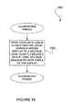
- FIG. 6shows a method 600 for illuminating pixels, in accordance with one embodiment.
- the method 600may be implemented in the context of the details of FIGS. 1-5 .
- the method 600may be carried out in any desired environment. Further, the aforementioned definitions may equally apply to the description below.
- a currentis applied to a data line coupled to a selected pixel.
- a data lineis a line that is capable of current flow.
- a voltageis stored in the pixel based on the current.
- operation 604includes manipulating a voltage on a select line coupled to the pixel for closing a first switch between the data line and a storage node, the storage node being coupled to a gate and an electrode of a second switch between the data line and a light emitting diode.
- a select lineis any line used to select and/or deselect a pixel or plurality of pixels for illumination. Further, after a period of time, the voltage is changed on the select line for opening the first switch, as shown in operation 606 .
- each storage nodeis returned to about a same voltage as the storage node had at an end of the line period, or to a lower voltage than the storage node had at an end of the line period.
- FIG. 7shows a method 700 for illuminating pixels, in accordance with another embodiment.
- the method 700may be implemented in the context of the details of FIGS. 1-5 .
- the method 700may be carried out in any desired environment. Further, the aforementioned definitions may equally apply to the description below.
- a currentis applied to a data line coupled to a selected pixel.
- a voltageis manipulated on a select line coupled to the pixel for closing a first switch between the data line and a storage node, the storage node being coupled to a gate and an electrode of a second switch between the data line and a light emitting diode.
- the voltageis changed on the select line for opening the first switch, as shown in operation 706 .
- each storage nodeis returned to a lower voltage than the storage node had at an end of the line period.
- FIG. 8shows a display driver 800 , in accordance with another embodiment.
- the display driver 800may be implemented in the context of the details of FIGS. 1-7 .
- the display driver 800may be carried out in any desired environment. Further, the aforementioned definitions may equally apply to the description below.
- a digital to analog converter 802producing a current at a selected level, an output of the digital to analog converter 802 being coupleable to a data line 804 of a display 806 .
- a second voltage source 808may be coupled to the data line 804 for precharging the data line 804 .
- FIG. 9shows a method 900 for precharging a data line of a display, in accordance with another embodiment.
- the method 900may be implemented in the context of the details of FIGS. 1-8 .
- the method 900may be carried out in any desired environment. Further, the aforementioned definitions may equally apply to the description below.
- a voltage level on every data lineis determined at the end of each select line period within a frame period.
- these voltage levelsare stored in a frame store memory. Further, prior to or during a subsequent frame period, each data line is precharged to a derivative of the stored voltage level for that select line period, as shown in operation 906 .
- FIG. 10shows a method 1000 for precharging a data line of a light emitting diode current-driven display, in accordance with one embodiment.
- the method 1000may be implemented in the context of the details of FIGS. 1-9 .
- the method 1000may be carried out in any desired environment. Further, the aforementioned definitions may equally apply to the description below.
- each data linemay be driven to a voltage level slightly below a black level voltage associated with the pixels of the display.
- FIG. 11shows a circuit 1100 for a 2-transistor Sequential Current Mirror (SCM) AMOLED pixel, in accordance with one embodiment. Portions or all of the circuit 1100 may be reproduced for each pixel in a given display. As an option, the circuit 1100 may be implemented in the context of the details of FIG. 1-10 . Of course, however, the circuit 1100 may be carried out in any desired environment. Further, the aforementioned definitions may equally apply to the description below.
- SCMSequential Current Mirror
- a data line 1104is provided, in addition to a select line 1116 . Further, a storage node 1114 is coupled to the select line 1116 . In addition, a first capacitance 1108 coupled between the storage node 1114 and the select line 1116 is provided.
- a first transistor 1120 with a gateis coupled to the select line 1116 , a first electrode thereof coupled to the storage node 1114 , and a second electrode thereof coupled to the data line 1104 . Still yet, a second transistor 1106 with a gate coupled to the storage node 1114 , a first electrode thereof coupled to the data line 1104 .
- an organic light emitting diode (OLED) 1112is coupled to a second electrode of the second transistor 1106 .
- OLEDorganic light emitting diode
- the circuit 1100is described utilizing an OLED, in another embodiment a LED or other current-driven pixel may similarly be used.
- the fastest operationis achieved by precharging each data line and pixel close to—but slightly to the dark side—of its “predicted settling voltage”.
- the “predicted settling voltage” for each pixelis computed as the voltage on the data line and pixel at the end of its select line period during the previous frame, with a correction voltage to account for brightness differences (if any) between the brightness data that was to have been displayed during the previous frame and the brightness data that is to be displayed during the current frame.
- the calculation of this correction voltageis done with a lookup table that is responsive to both the previous frame data and current frame data for that pixel.
- Best operationis usually achieved by further adjusting the actual precharge voltage to a level about 0.1V different from the “predicted settling voltage” such that the pixel conducts slightly less current immediately after the precharge than it would if it were precharged exactly to its “predicted settling voltage.” This way, each pixel usually transitions from a darker state towards lighter state during the current-mode interval which follows the precharge interval during the select line time. Any excess charge on the data line is thereby rapidly removed by the precharge instead of having to discharge slowly through the pixel itself.
- a reference or “programming” currentmay be applied to the data line 1104 and forced to flow through the second transistor 1106 which has its gate and drain nodes connected together.
- transistor 1106has no physical mirror transistor. Instead, as shown, the gate voltage of the second transistor 1106 , developed in response to the programming current, is first stored on the first capacitor 1108 and a second capacitor 1110 (shown as part of the storage node 1114 ), and then used later to drive a mirror version of that same current through the OLED 1112 .
- the second transistor 1106may be viewed as its own “mirrored output” transistor, as the second transistor 1106 is used for both a reference transistor and an output transistor. Using the same transistor sequentially as both the reference transistor and the output transistor, allows for the second transistor 1106 to be a perfect mirror match to itself. This results in a simple but elegant sample-and-hold circuit that first “samples” the program current, and then produces a scaled replica of that current during an extended “illumination” period.
- circuit 1100is extremely accurate and uniform due to the current programming that compensates for variations and drift in the transistor threshold.
- the circuit 1100also effectively compensates for transistor threshold and mobility variations, and non-uniformities and drift in OLED offset voltages.
- circuit 1100is shown for NMOS transistors driving the anode of the OLED with a common cathode, in another embodiment the circuit may be varied to drive the OLED cathode. In other embodiments, PMOS and CMOS transistors may also be used in independently or in conjunction with NMOS transistors.
- the first capacitor 1108 and the second capacitor 1110may be sized by deliberate layout choices to control the natural parasitic capacitances that are an intrinsic part of the transistors themselves. In another embodiment, the first capacitor 1108 and the second capacitor 1110 may be added during pixel layout.
- the circuit 1100may be designed such that the capacitance of the first capacitor 1108 and the capacitance of the second capacitor 1110 are equal. Further, for operation in High-Speed Mode, the first capacitor 1108 may be made about 20% larger than the second capacitor 1110 . Such High-Speed Operation of Current-Mode Pixels is described in more detail below.
- the circuit 1100will be used to describe possible operation of the circuit with the first capacitor 1108 equal to the second capacitor 1110 and no other significant capacitance loading the storage node 1114 .
- the circuit 1100receives, stores, and provides the current necessary to display a bright gray-scale level (8 ⁇ A) and a moderately-dark gray-scale level (0.016 MA) with a contrast ratio of 500:1.
- the voltage at the storage node 1114normally ranges from a 1V black level to 4V maximum white level referenced to a state where all other nodes connected to the circuit were grounded.
- the pixel voltage at the storage node 1114may be referenced to another condition.
- a current-mode data line driver 1102begins injecting 8 ⁇ A onto the data line 1104 and the select line 1116 that has been selected is raised to 10V. It should be noted that, initially, a common node 1118 is held constant at ⁇ 10V. Once the first transistor 1120 begins to conduct, the storage node 1114 is directly connected to the data line 1104 . Since a selected row of pixels all have +10V on their select lines (e.g., the select line 1116 ) and ⁇ 10V on their load terminals (e.g., the common node 1118 ), their storage nodes (e.g., the storage node 1114 ) will be at their referenced condition (e.g., IV to 4V).
- Vstoredis the voltage at the storage node 1114
- C1 and C2are the capacitances of the first capacitor 1108 and the second capacitor 1110 , respectively
- Vselectis the voltage of the select line 1116
- Vcommonis the voltage at the common node 1118 .
- the second transistor 1106has negative voltage on its gate and is therefore non-conducting for all the deselected pixels.
- the 8 ⁇ A current from the current-mode data line driver 1102therefore must all flow through the second transistors 1106 in the selected pixels.
- the select line 1116 voltage for the deselected pixelsmust be even more negative than the lowest voltage stored on the storage node 1114 to insure that the first transistor 1120 is also always turned off for the deselected pixels.
- the voltage on the storage node 1114will either rise or fall to the exact voltage level to permit the second transistor 1106 to conduct the 8 ⁇ A current. For example, if the voltage on the storage node 1114 is initially too low to permit the second transistor 1106 to conduct, less than 8 pA will flow through the second transistor 1106 and some of the excess current from the data line 1104 will then flow through the first transistor 1120 into the storage node 1114 to raise the voltage at the storage node 1114 .
- the current-mode data line driver 1102injects only 0.016 ⁇ A onto the data line 1104 .
- the voltage on the storage node 1114will either rise or fall to the exact voltage level to permit the second transistor 1106 to conduct the 0.016 ⁇ A current.
- the voltage on the storage node 1114is initially lower than it should be, less than 0.016 ⁇ A will flow through the second transistor 1106 and some of the excess current from the data line 1104 will then flow through the first transistor 1120 into the storage node 1114 to raise the voltage of the storage node 1114 .
- the current flowing through the second transistor 1106will be more than 0.016 ⁇ A and the excess current flowing through the second transistor 1106 will pull current back through both the second transistor 1106 and the first transistor 1120 until the voltage on the storage node 1114 reaches the right value. Therefore the voltage stored at the storage node 1114 at the end of the line period is just sufficient to drive 0.016 ⁇ A through the second transistor 1106 and the OLED 1112 and thereby compensates for the variations in the forward drop of the OLED 1112 , the threshold voltage of the second transistor 1106 , power supply variations, and the mobility of the second transistor 1106 .
- the select line 1116is returned to its deselected ⁇ 10V level which turns off the first transistor 1120 and locks and stores the correct voltage at the storage node 1114 . Deselecting this pixel or array of pixels (e.g. a row of pixels) also drives the voltage at the storage node 1114 negative to terminate any flow of current through the second transistor 1106 .
- each row of pixelsis alternately selected and deselected in sequence and the proper voltages stored in their respective pixels. Only minimal light is generated during this frame period.
- the frame periodalso includes an illumination period.
- the illumination periodis 20% of the frame period, the equivalent of 256 line periods out of 1280 (1024+256) total line periods.
- This illumination periodmay be divided into 16 sub-periods of 16 line periods each wherein an illumination sub-period is inserted after each block of 64 line load periods.
- the entire 256 line illumination periodwould be inserted after scanning through all select lines to significantly reduce the kinds of motion artifacts that are normally associated with other conventional sample-and-hold displays like AMOLEDs and AMLCDs.
- an active matrix displaymay be 256 times brighter than a simple line-at-a-time display wherein each pixel only produces light during one line period instead of 256 line periods.
- the voltage levelsmay be adjusted as necessary to achieve either higher brightness or higher power efficiency. For example, if more voltage is desired to drive the OLED 1112 , the data line 1104 voltage level could be raised to 10V in order to store a wider range of voltages in the circuit 1100 (1-10V). Furthermore, during the illuminate period, the data line 1104 could be clamped either higher or lower than this 4V level.
- higher power efficiencymay be achieved (e.g. with a small compromise to mobility compensation in the brightest pixels) by programming all pixels at 10V, but providing about 4V during the illumination period.
- the second transistor 1106may now operate in the more power efficient “bootstrapped” or “triode” mode for the brightest pixels to provide extremely power-efficient operation in the array. It should be noted that when the display is operating at maximum brightness over 99% of the light is generated during the illumination period—while less than 1% is generated during the load and programming periods. Therefore, providing a higher voltage during the load and programming periods does not significantly affect the operating power efficiency of the display. Although the overall gamma characteristic would be slightly flattened by operating the second transistor 1106 in the triode mode, this effect can be easily corrected by the gamma correction circuit mentioned in the disclosure.
- the SCM arraycould be operated exclusively in the saturation mode to provide the best uniformity and accuracy, in most applications we will be able to reduce the illumination voltage to its lowest possible voltage to maximize power efficiency, and let the second transistor 1106 drop into its triode region without significantly degrading the image quality of the display. Even in its triode region the pixel continues to provide excellent cancellation for the OLED 1112 offset voltage variations and resistance, variability in TFT Vt, and the power supply variations. Only its compensation for TFT mobility would be significantly reduced and these mobility variations aren't usually the biggest source of gray scale variations anyway. And even under these conditions the second transistor 1106 would continue to operate in its saturation mode for all of the gray scale levels below that of the brightest pixels. So while the pixel compensation is best at higher data line voltages, this pixel still provides excellent compensation and uniformity even when operating in a low-data-line-voltage ultra-high-efficiency mode.
- the voltage loss in the pixelis minimized by using only one transistor between the power supply and the OLED 1112 compares other OLED pixels which require the OLED 1112 current to pass through two transistors connected in series.
- the dark gray-scale level transient responsewill be even slower than the brighter pixels.
- the data line time constant for this dark gray-scale pixelis now 700 times longer than the entire select line period and at least 200 times longer than would be tolerable in a practical array.
- the pixelis adjusted so that the voltage stored at storage node 1114 during the illumination period is slightly less (in this example by 1 V) than what was stored during the line mode. This can be easily be achieved by making capacitor 1108 20% larger than capacitor 1110 . It can also be achieved by simply lowering the voltage on the common node slightly during the illuminate period from +10V to approximately +6V.
- the currents flowing through transistor 1106 and the OLED during both the line period and illuminate periodare then as shown in the chart 1200 of FIG. 12 .
- the OLED currentsare plotted as a linear function of the stored voltage at storage node 1114 during the select line period.
- the peak current flowing during the selected line periodis shown.
- the plot of peak illuminate-period currentlooks the same as the plot of peak line-time current except that it has now been shifted to the right by exactly 1V. Note that the peak line-time pixel current is always larger than the peak illuminate-period pixel current.
- FIG. 13is a chart 1300 of the data from FIG. 12 , on a semi-log scale. Note that the square-law variation of current vs. voltage that looks steep in FIG. 12 , does not look nearly as steep in the semi-log plot 1300 in FIG. 13 .
- the semi-log plot 1300 in FIG. 13also shows other important effects that were hidden in FIG. 12 including the sub-threshold currents flowing during both the line-select period and the illuminate periods.
- FIG. 13also shows the time-averaged line-time and illumination-period currents. Since the line-time current only flows for 1 line period out of 1280 line periods in the frame the average line-time current is quite low.
- the average illumination period currentis 20% as high as the peak illumination period current. Note that when the pixel voltage exceeds 1.8V, the average illumination period current is now much larger than the average line-time current.
- FIG. 14is a plot 1400 of the pixel brightness in foot lamberts as a function of the voltage stored at storage node 1114 at the end of the select period.
- the peak brightness level of 100 flis achieved with 4V stored at storage node 1114 .
- the gamma curve for the pixel shown in FIG. 14is a good match to the human visual system and is easily mapped into the gamma 2.3 curve commonly used in photography and TV.
- FIG. 15is a chart 1500 showing how this unbalanced SCM pixel design solves the speed problem afflicting both the nominal 2Q design and all of the other current-driven displays.
- the maximum peak current flowing during the select line periodis now slightly higher since the illumination period peak current is only about half of the line time peak programming current such that the illumination-average-current is now less than 256 times as high as the average-line-current.
- the peak line current corresponding to the 1.35V level that is stored in the pixel to provide the 0.2 fl pixel brightness for a contract ratio of 500:1,corresponds to 11% of the current required to provide the 100 fl brightness described above.
- ⁇ Vcan be reduced to about 0.1 V which further reduces the data line delay to only 1.8 ⁇ s even for the worst case dark pixels.
- the 1.8 ⁇ s delayis now fast enough for all display applications.
- the new high-speed pixel in this exemplary embodimentachieves a brightness ratio of 500:1 with a line current ratio of only 9:1. Even extreme contrast ratios of 5,000:1 are achieved with a line current ratio of only 30:1.
- This unexpected resultis achieved because the display and pixel operates at lower voltages in a line-illumination mode where it works like a passive matrix OLED display, then gradually transitions above 2V to operate in a frame-illumination mode like a traditional Active Matrix OLED which multiplies its brightness by more than 100 times.
- the illumination-period-to-line-period-ratio(256 ⁇ ) effectively multiplies and extends the current ratio on the data line (9 ⁇ ) to produce high-contrast displays without creating large and variable delays in charging and discharging the data lines.
- a fundamental problem limiting the deployment of current-driven OLED pixelshas now been solved.
- the new gamma curve shown in FIG. 15provides much more accurate control of dark pixels compared to a conventional square-law display pixel where a fixed change in the voltage stored in the pixel produces a much bigger percentage change in dark pixels than it does in the bright pixels.
- the new gamma curve shown in FIG. 15yields a steeper-than-square-law relationship between the pixel voltage and brightness, which corresponds better to the way the eye perceives light. Control of dark pixels is therefore roughly 10 times as accurate as using a conventional pure square-law pixel.
- FIG. 16provides details on the design of a simple current-mode data line driver 1600 that can be used to drive the SCM pixel.
- a digital industry-standard de-multiplexeris used to load and store the digital information to be displayed during one line time.
- the 8 binary outputsswitch various combinations of 8 p-type transistors in or out of the circuit. Each of these 8 transistors is twice as big and conducts exactly twice as much current as the one immediately to the right of it. This array injects any one of 256 different current levels onto the data line.
- a good uniform black levelis insured by precharging (at the beginning of every line period) every data line to a voltage level slightly below the black level voltage for node-A in the pixels.
- the charge and discharge of the data lines of current-mode displayscan be made faster by combining use of the current driver described in FIG. 16 with the analog voltage driver shown in FIG. 17 to create the circuit 1700 shown.
- the analog voltage driverpre-charges each data line to approximately the voltage needed to supply the desired current to each pixel.
- This “precharge voltage”is calculated by first measuring and storing in a frame store memory the voltage level that had been present on that data line at the end of the line period for that same pixel during the previous frame period. This “frame store” voltage level is then adjusted for any brightness level differences at this pixel between the brightness-level data provided during the last frame and the brightness-level data provided during the current frame based on a simple fixed lookup table. This adaptive, iterative, and accurate method generates a different precharge level for each pixel. In this way the system accurately and adaptively predicts the required voltage and will quickly precharge that data line close to—and preferably slightly below—this level at the beginning of its line period.
- This analog voltage prechargeis typically completed within 2 ⁇ s after which the data line driver reverts to its current drive mode to permit the current and voltage levels to settle out to their final values.
- This adaptive frame-store-based precharge circuit and method described hereinwill be accurate to better than 0.5V even for a rapidly changing image, reducing the slew voltage from 5V to 0.5V and reducing the data line delay by a factor of 10:1.
- this adaptive precharge circuitcan reduce the residual precharge error to less than 0.1V—which in this example will reduce the data-line settling time to only 1.8 ⁇ s.
- Both the circuits shown in FIGS. 16 and 17are adjusted to precharge the data lines slightly below the final voltage. This biases the pixel to transition through a slightly darker state during steady-state or light-to-dark-state transitions. This in turn provides cleaner black levels and a better dynamic response than the opposite condition wherein the pixel might otherwise transition through a brighter state during steady-state or light-to-dark-state transitions.
- each data line driver(or cluster of data line drivers) may require a negative voltage feedback circuit similar to voltage regulation circuits used in design of regulated power supplies.
Landscapes
- Engineering & Computer Science (AREA)
- Physics & Mathematics (AREA)
- Computer Hardware Design (AREA)
- General Physics & Mathematics (AREA)
- Theoretical Computer Science (AREA)
- Control Of El Displays (AREA)
- Control Of Indicators Other Than Cathode Ray Tubes (AREA)
Abstract
Description
t=ΔV*C/I=5*40×10−12/8×10−6=25 μs
which is a problem since it is larger than a line period of typically 16 μs. However, like other current-driven active-matrix pixels, the dark gray-scale level transient response will be even slower than the brighter pixels. In our example with a contrast ratio of 500:1, the dark pixels conduct only 16 nA and the settling time on the data line is much slower:
t=ΔV*C/I=5*40×10−12/0.016×10−6=12,000 μs
- (1) Modifying the capacitor values in the pixel to cause the pixel to transition gradually from line mode of operation to a frame mode of operation as the brightness increases from minimum to maximum. This also greatly improves the accuracy and uniformity of the display gray scale levels especially in the low-brightness areas of the screen.
- (2) Adding a voltage precharge circuit to the data decoder to reduce settling time on the data lines.
Ipeak line=Inominal(Va−Vt)2/(Va−Vt−1V)2=8 μA(4V−1V)2/(4V−2V)2/(4V−2V)2=20 μA
The data line delay is now:
t=ΔV*C/I=5*40×10−12/20×10−6=10 μs
which is a little faster but not greatly different from the 25 μs delay achieved above. However the line delay for the dark pixel has been improved dramatically. From
t=ΔV*C/I=5*40×10−12/2.2×10−6=90 μs
Compared with the 12,000 μs delay suffered in the nominal pixel, this higher-speed design is more than 100 times faster and is now adequate for many display applications. Also as long as pixels of different colors are not connected to the same data line (as is usually the case), then even without a line precharge, data line delays of several times the line time may be tolerated without creating significant visually-perceptual degradation of the image. Using the advanced adaptive precharge circuit shown in the “High Speed Data Line Drivers with Voltage Precharge” section below, ΔV can be reduced to about 0.1 V which further reduces the data line delay to only 1.8 μs even for the worst case dark pixels. The 1.8 μs delay is now fast enough for all display applications.
Claims (19)
Priority Applications (2)
| Application Number | Priority Date | Filing Date | Title |
|---|---|---|---|
| US12/692,453US8531359B2 (en) | 2006-06-16 | 2010-01-22 | Pixel circuits and methods for driving pixels |
| US14/022,186US8937582B2 (en) | 2006-06-16 | 2013-09-09 | Pixel circuit display driver |
Applications Claiming Priority (3)
| Application Number | Priority Date | Filing Date | Title |
|---|---|---|---|
| US80505806P | 2006-06-16 | 2006-06-16 | |
| US11/759,796US7679586B2 (en) | 2006-06-16 | 2007-06-07 | Pixel circuits and methods for driving pixels |
| US12/692,453US8531359B2 (en) | 2006-06-16 | 2010-01-22 | Pixel circuits and methods for driving pixels |
Related Parent Applications (1)
| Application Number | Title | Priority Date | Filing Date |
|---|---|---|---|
| US11/759,796DivisionUS7679586B2 (en) | 2006-06-16 | 2007-06-07 | Pixel circuits and methods for driving pixels |
Related Child Applications (1)
| Application Number | Title | Priority Date | Filing Date |
|---|---|---|---|
| US14/022,186DivisionUS8937582B2 (en) | 2006-06-16 | 2013-09-09 | Pixel circuit display driver |
Publications (2)
| Publication Number | Publication Date |
|---|---|
| US20100118018A1 US20100118018A1 (en) | 2010-05-13 |
| US8531359B2true US8531359B2 (en) | 2013-09-10 |
Family
ID=39150771
Family Applications (3)
| Application Number | Title | Priority Date | Filing Date |
|---|---|---|---|
| US11/759,796Expired - Fee RelatedUS7679586B2 (en) | 2006-06-16 | 2007-06-07 | Pixel circuits and methods for driving pixels |
| US12/692,453Active2029-03-12US8531359B2 (en) | 2006-06-16 | 2010-01-22 | Pixel circuits and methods for driving pixels |
| US14/022,186ActiveUS8937582B2 (en) | 2006-06-16 | 2013-09-09 | Pixel circuit display driver |
Family Applications Before (1)
| Application Number | Title | Priority Date | Filing Date |
|---|---|---|---|
| US11/759,796Expired - Fee RelatedUS7679586B2 (en) | 2006-06-16 | 2007-06-07 | Pixel circuits and methods for driving pixels |
Family Applications After (1)
| Application Number | Title | Priority Date | Filing Date |
|---|---|---|---|
| US14/022,186ActiveUS8937582B2 (en) | 2006-06-16 | 2013-09-09 | Pixel circuit display driver |
Country Status (1)
| Country | Link |
|---|---|
| US (3) | US7679586B2 (en) |
Families Citing this family (9)
| Publication number | Priority date | Publication date | Assignee | Title |
|---|---|---|---|---|
| US8446394B2 (en)* | 2006-06-16 | 2013-05-21 | Visam Development L.L.C. | Pixel circuits and methods for driving pixels |
| US20080062090A1 (en)* | 2006-06-16 | 2008-03-13 | Roger Stewart | Pixel circuits and methods for driving pixels |
| US7679586B2 (en)* | 2006-06-16 | 2010-03-16 | Roger Green Stewart | Pixel circuits and methods for driving pixels |
| WO2009035588A1 (en)* | 2007-09-12 | 2009-03-19 | Corning Incorporated | Derivative sampled, fast settling time current driver |
| JP2009276671A (en)* | 2008-05-16 | 2009-11-26 | Canon Inc | Light-emitting device |
| LU92598B1 (en)* | 2014-11-17 | 2016-05-18 | Universität des Saarlandes | A local dimming algorithm and device |
| WO2016129463A1 (en)* | 2015-02-10 | 2016-08-18 | シャープ株式会社 | Display device and method for driving same |
| US9836173B2 (en) | 2016-03-30 | 2017-12-05 | Synaptics Incorporated | Optimizing pixel settling in an integrated display and capacitive sensing device |
| US9983721B2 (en) | 2015-12-31 | 2018-05-29 | Synaptics Incorporated | Optimizing pixel settling in an integrated display and capacitive sensing device |
Citations (76)
| Publication number | Priority date | Publication date | Assignee | Title |
|---|---|---|---|---|
| US5686935A (en) | 1995-03-06 | 1997-11-11 | Thomson Consumer Electronics, S.A. | Data line drivers with column initialization transistor |
| US5751279A (en) | 1992-07-16 | 1998-05-12 | Nec Corporation | Active matrix type liquid crystal display and method driving the same |
| US6157356A (en) | 1996-04-12 | 2000-12-05 | International Business Machines Company | Digitally driven gray scale operation of active matrix OLED displays |
| US6229506B1 (en) | 1997-04-23 | 2001-05-08 | Sarnoff Corporation | Active matrix light emitting diode pixel structure and concomitant method |
| US6229508B1 (en) | 1997-09-29 | 2001-05-08 | Sarnoff Corporation | Active matrix light emitting diode pixel structure and concomitant method |
| US6307322B1 (en) | 1999-12-28 | 2001-10-23 | Sarnoff Corporation | Thin-film transistor circuitry with reduced sensitivity to variance in transistor threshold voltage |
| US20020047568A1 (en) | 2000-07-27 | 2002-04-25 | Semiconductor Energy Laboratory Co., Ltd. | Method of driving display device |
| WO2002091341A2 (en) | 2001-05-09 | 2002-11-14 | Clare Micronix Integrated Systems, Inc. | Apparatus and method of periodic voltage sensing for control of precharging of a pixel |
| US20030016201A1 (en) | 2001-07-14 | 2003-01-23 | Koninklijke Philips Electronics N.V. | Active matrix display devices |
| US20030038760A1 (en) | 2001-08-25 | 2003-02-27 | Kim Chang Yeon | Apparatus and method for driving electro-luminescence panel |
| WO2003034390A2 (en) | 2001-10-19 | 2003-04-24 | Clare Micronix Integrated Systems, Inc. | Precharge circuit and method for passive matrix oled display |
| US20030090446A1 (en) | 2001-11-09 | 2003-05-15 | Akira Tagawa | Display and driving method thereof |
| US20030095087A1 (en) | 2001-11-20 | 2003-05-22 | International Business Machines Corporation | Data voltage current drive amoled pixel circuit |
| US20030107565A1 (en) | 2001-11-20 | 2003-06-12 | International Business Machines Corporation | Active matrix oled voltage drive pixel circuit |
| US20030111966A1 (en) | 2001-12-19 | 2003-06-19 | Yoshiro Mikami | Image display apparatus |
| US20030128200A1 (en) | 2000-11-07 | 2003-07-10 | Akira Yumoto | Active matrix display and active matrix organic electroluminescence display |
| US6594606B2 (en) | 2001-05-09 | 2003-07-15 | Clare Micronix Integrated Systems, Inc. | Matrix element voltage sensing for precharge |
| US20030151564A1 (en) | 2001-10-17 | 2003-08-14 | Junichi Yamashita | Display apparatus |
| US20040017162A1 (en) | 2002-03-04 | 2004-01-29 | Hitachi, Ltd. | Organic electroluminescent light emitting display device |
| US6693385B2 (en) | 2001-03-22 | 2004-02-17 | Semiconductor Energy Laboratory Co., Ltd. | Method of driving a display device |
| US20040041766A1 (en) | 2000-07-19 | 2004-03-04 | Kenji Nakao | Ocb liquid crystal display with active matrix and supplemental capacitors and driving method for the same |
| US20040080470A1 (en) | 2000-02-29 | 2004-04-29 | Semiconductor Energy Laboratory Co., Ltd., A Japan Corporation | Light-emitting device |
| US20040087066A1 (en) | 2002-07-11 | 2004-05-06 | Sharp Laboratories Of America, Inc. | Flexible metal foil substrate display and method for forming same |
| US6734636B2 (en) | 2001-06-22 | 2004-05-11 | International Business Machines Corporation | OLED current drive pixel circuit |
| US20040095297A1 (en) | 2002-11-20 | 2004-05-20 | International Business Machines Corporation | Nonlinear voltage controlled current source with feedback circuit |
| US20040150591A1 (en) | 1997-02-17 | 2004-08-05 | Seiko Epson Corporation | Display apparatus |
| US20040160394A1 (en) | 2003-02-14 | 2004-08-19 | Elantec Semiconductor, Inc. | Methods and systems for driving displays including capacitive display elements |
| US20040174349A1 (en) | 2003-03-04 | 2004-09-09 | Libsch Frank Robert | Driving circuits for displays |
| US20040179005A1 (en) | 2003-02-19 | 2004-09-16 | Seiko Epson Corporation | Electro-optical device, method of driving electro-optical device, and electronic apparatus |
| US6809706B2 (en) | 2001-08-09 | 2004-10-26 | Nec Corporation | Drive circuit for display device |
| US20040252088A1 (en) | 2003-06-16 | 2004-12-16 | Genshiro Kawachi | Organic EL light emitting display device |
| US20050007361A1 (en) | 2003-07-10 | 2005-01-13 | Nec Electronics Corporation | Current-driven active matrix display panel for improved pixel programming |
| US6847340B2 (en) | 2002-08-16 | 2005-01-25 | Windell Corporation | Active organic light emitting diode drive circuit |
| US20050030264A1 (en) | 2001-09-07 | 2005-02-10 | Hitoshi Tsuge | El display, el display driving circuit and image display |
| US20050041002A1 (en) | 2001-09-07 | 2005-02-24 | Hiroshi Takahara | El display panel, its driving method, and el display apparatus |
| US20050046619A1 (en) | 2003-08-28 | 2005-03-03 | Sharp Kabushiki Kaisha | Driving circuit for display device, and display device |
| US6864639B2 (en) | 2002-09-10 | 2005-03-08 | Dai Nippon Printing Co, Ltd | Display and method for manufacturing the same |
| US20050068270A1 (en)* | 2003-09-17 | 2005-03-31 | Hiroki Awakura | Display apparatus and display control method |
| US20050068271A1 (en) | 2003-09-29 | 2005-03-31 | Shin-Tai Lo | Active matrix organic electroluminescence display driving circuit |
| US20050067971A1 (en) | 2003-09-29 | 2005-03-31 | Michael Gillis Kane | Pixel circuit for an active matrix organic light-emitting diode display |
| US6885356B2 (en) | 2000-07-18 | 2005-04-26 | Nec Electronics Corporation | Active-matrix type display device |
| US20050104819A1 (en) | 2003-11-07 | 2005-05-19 | Nec Corporation | Semiconductor device for driving current load device, and display device |
| US20050105031A1 (en) | 2003-11-13 | 2005-05-19 | Po-Sheng Shih | [pixel structure of display and driving method thereof] |
| US20050110725A1 (en) | 2003-11-26 | 2005-05-26 | Won-Kyu Kwak | Flat panel display device with triodic rectifier switch |
| US20050140610A1 (en) | 2002-03-14 | 2005-06-30 | Smith Euan C. | Display driver circuits |
| US6930680B2 (en) | 2001-12-13 | 2005-08-16 | Seiko Epson Corporation | Pixel circuit for light emitting element |
| US20050179399A1 (en) | 2004-01-16 | 2005-08-18 | Karl Leo | Pixel for an active matrix display |
| US6943761B2 (en) | 2001-05-09 | 2005-09-13 | Clare Micronix Integrated Systems, Inc. | System for providing pulse amplitude modulation for OLED display drivers |
| US6943500B2 (en) | 2001-10-19 | 2005-09-13 | Clare Micronix Integrated Systems, Inc. | Matrix element precharge voltage adjusting apparatus and method |
| US20050200618A1 (en) | 2004-03-09 | 2005-09-15 | Yang-Wan Kim | Light-emitting display |
| US20050206591A1 (en) | 2004-03-18 | 2005-09-22 | Wen-Chun Wang | Active matrix organic electroluminescence light emitting diode driving circuit |
| US20050212787A1 (en) | 2004-03-24 | 2005-09-29 | Sanyo Electric Co., Ltd. | Display apparatus that controls luminance irregularity and gradation irregularity, and method for controlling said display apparatus |
| US20050219163A1 (en) | 2002-04-25 | 2005-10-06 | Smith Euan C | Display driver circuits for organic light emitting diode displays with skipping of blank lines |
| US20050218791A1 (en) | 2001-01-31 | 2005-10-06 | Seiko Epson Corporation | Display device |
| US20050243031A1 (en) | 2002-09-05 | 2005-11-03 | Koninklijke Philips Electronics, N. V. | Electroluminescent display devices |
| US20050243038A1 (en) | 2004-04-29 | 2005-11-03 | Won-Kyu Kwak | Light emitting panel and light emitting display |
| US20050242743A1 (en) | 2004-04-29 | 2005-11-03 | Won-Kyu Kwak | Light emitting panel and light emitting display |
| US6970149B2 (en) | 2002-09-14 | 2005-11-29 | Electronics And Telecommunications Research Institute | Active matrix organic light emitting diode display panel circuit |
| US20050264228A1 (en) | 2004-05-25 | 2005-12-01 | Keum-Nam Kim | Organic electro luminescent display panel and fabricating method thereof |
| US6972742B2 (en) | 2001-05-09 | 2005-12-06 | Clare Micronix Integrated Systems, Inc. | Method of current balancing in visual display devices |
| US20050275352A1 (en) | 2004-06-14 | 2005-12-15 | Au Optronics Corporation. | Redundant storage capacitor and method for repairing OLED pixels and driving circuits |
| US20050285822A1 (en) | 2004-06-29 | 2005-12-29 | Damoder Reddy | High-performance emissive display device for computers, information appliances, and entertainment systems |
| US20050285827A1 (en) | 2004-06-29 | 2005-12-29 | Ki-Myeong Eom | Light emitting display |
| US20060001613A1 (en) | 2002-06-18 | 2006-01-05 | Routley Paul R | Display driver circuits for electroluminescent displays, using constant current generators |
| US6989826B2 (en) | 2001-08-02 | 2006-01-24 | Seiko Epson Corporation | Driving of data lines used in unit circuit control |
| US20060044236A1 (en) | 2004-08-25 | 2006-03-02 | Kim Yang W | Light emitting display and driving method including demultiplexer circuit |
| US20060077137A1 (en) | 2004-10-08 | 2006-04-13 | Oh-Kyong Kwon | Data driving apparatus in a current driving type display device |
| US20060118700A1 (en) | 2004-12-06 | 2006-06-08 | Stmicroelectronics S.A. | Automatic adaptation of the precharge voltage of an electroluminescent display |
| US7079130B2 (en) | 2001-05-09 | 2006-07-18 | Clare Micronix Integrated Systems, Inc. | Method for periodic element voltage sensing to control precharge |
| US20070132674A1 (en) | 2003-12-02 | 2007-06-14 | Toshiba Matsushita Display Technology Co., Ltd. | Driving method of self-luminous type display unit, display control device of self-luminous type display unit, current output type drive circuit of self-luminous type display unit |
| US20080055223A1 (en) | 2006-06-16 | 2008-03-06 | Roger Stewart | Pixel circuits and methods for driving pixels |
| US20080062090A1 (en) | 2006-06-16 | 2008-03-13 | Roger Stewart | Pixel circuits and methods for driving pixels |
| US20080062091A1 (en) | 2006-06-16 | 2008-03-13 | Roger Stewart | Pixel circuits and methods for driving pixels |
| US7382341B2 (en)* | 2002-12-31 | 2008-06-03 | Lg Display Co., Ltd. | Organic electroluminescent device and driving method thereof |
| US7463229B2 (en) | 2003-07-18 | 2008-12-09 | Seiko Epson Corporation | Display driver, display device, and drive method |
| US7477248B2 (en) | 2002-11-15 | 2009-01-13 | Koninklijke Philips Electronics N.V. | Display device, electric device comprising such a display device and method for driving a display device |
Family Cites Families (4)
| Publication number | Priority date | Publication date | Assignee | Title |
|---|---|---|---|---|
| US5689935A (en) | 1996-03-11 | 1997-11-25 | Recot, Inc. | Product package having reliable openability |
| US7209101B2 (en)* | 2001-08-29 | 2007-04-24 | Nec Corporation | Current load device and method for driving the same |
| JP3830888B2 (en)* | 2002-12-02 | 2006-10-11 | オプトレックス株式会社 | Driving method of organic EL display device |
| JP2006039456A (en)* | 2004-07-30 | 2006-02-09 | Oki Electric Ind Co Ltd | Driving circuit and driving method for panel display device |
- 2007
- 2007-06-07USUS11/759,796patent/US7679586B2/ennot_activeExpired - Fee Related
- 2010
- 2010-01-22USUS12/692,453patent/US8531359B2/enactiveActive
- 2013
- 2013-09-09USUS14/022,186patent/US8937582B2/enactiveActive
Patent Citations (88)
| Publication number | Priority date | Publication date | Assignee | Title |
|---|---|---|---|---|
| US5751279A (en) | 1992-07-16 | 1998-05-12 | Nec Corporation | Active matrix type liquid crystal display and method driving the same |
| US5686935A (en) | 1995-03-06 | 1997-11-11 | Thomson Consumer Electronics, S.A. | Data line drivers with column initialization transistor |
| US6157356A (en) | 1996-04-12 | 2000-12-05 | International Business Machines Company | Digitally driven gray scale operation of active matrix OLED displays |
| US6839045B2 (en) | 1997-02-17 | 2005-01-04 | Seiko Epson Corporation | Display apparatus |
| US20040150591A1 (en) | 1997-02-17 | 2004-08-05 | Seiko Epson Corporation | Display apparatus |
| US6229506B1 (en) | 1997-04-23 | 2001-05-08 | Sarnoff Corporation | Active matrix light emitting diode pixel structure and concomitant method |
| US6618030B2 (en) | 1997-09-29 | 2003-09-09 | Sarnoff Corporation | Active matrix light emitting diode pixel structure and concomitant method |
| US6229508B1 (en) | 1997-09-29 | 2001-05-08 | Sarnoff Corporation | Active matrix light emitting diode pixel structure and concomitant method |
| US20010024186A1 (en) | 1997-09-29 | 2001-09-27 | Sarnoff Corporation | Active matrix light emitting diode pixel structure and concomitant method |
| US6307322B1 (en) | 1999-12-28 | 2001-10-23 | Sarnoff Corporation | Thin-film transistor circuitry with reduced sensitivity to variance in transistor threshold voltage |
| US20040080470A1 (en) | 2000-02-29 | 2004-04-29 | Semiconductor Energy Laboratory Co., Ltd., A Japan Corporation | Light-emitting device |
| US6885356B2 (en) | 2000-07-18 | 2005-04-26 | Nec Electronics Corporation | Active-matrix type display device |
| US20040041766A1 (en) | 2000-07-19 | 2004-03-04 | Kenji Nakao | Ocb liquid crystal display with active matrix and supplemental capacitors and driving method for the same |
| US20020047568A1 (en) | 2000-07-27 | 2002-04-25 | Semiconductor Energy Laboratory Co., Ltd. | Method of driving display device |
| US20040012550A1 (en) | 2000-07-27 | 2004-01-22 | Semiconductor Energy Laboratory Co., Ltd. | Method of driving display device |
| US20030128200A1 (en) | 2000-11-07 | 2003-07-10 | Akira Yumoto | Active matrix display and active matrix organic electroluminescence display |
| US20050218791A1 (en) | 2001-01-31 | 2005-10-06 | Seiko Epson Corporation | Display device |
| US6693385B2 (en) | 2001-03-22 | 2004-02-17 | Semiconductor Energy Laboratory Co., Ltd. | Method of driving a display device |
| US7079130B2 (en) | 2001-05-09 | 2006-07-18 | Clare Micronix Integrated Systems, Inc. | Method for periodic element voltage sensing to control precharge |
| US6963321B2 (en) | 2001-05-09 | 2005-11-08 | Clare Micronix Integrated Systems, Inc. | Method of providing pulse amplitude modulation for OLED display drivers |
| US6594606B2 (en) | 2001-05-09 | 2003-07-15 | Clare Micronix Integrated Systems, Inc. | Matrix element voltage sensing for precharge |
| US6943761B2 (en) | 2001-05-09 | 2005-09-13 | Clare Micronix Integrated Systems, Inc. | System for providing pulse amplitude modulation for OLED display drivers |
| WO2002091341A2 (en) | 2001-05-09 | 2002-11-14 | Clare Micronix Integrated Systems, Inc. | Apparatus and method of periodic voltage sensing for control of precharging of a pixel |
| US6972742B2 (en) | 2001-05-09 | 2005-12-06 | Clare Micronix Integrated Systems, Inc. | Method of current balancing in visual display devices |
| US6965360B2 (en) | 2001-05-09 | 2005-11-15 | Clare Micronix Integrated Systems, Inc. | Method of current matching in integrated circuits |
| US6734636B2 (en) | 2001-06-22 | 2004-05-11 | International Business Machines Corporation | OLED current drive pixel circuit |
| US6897843B2 (en) | 2001-07-14 | 2005-05-24 | Koninklijke Philips Electronics N.V. | Active matrix display devices |
| US20030016201A1 (en) | 2001-07-14 | 2003-01-23 | Koninklijke Philips Electronics N.V. | Active matrix display devices |
| US6989826B2 (en) | 2001-08-02 | 2006-01-24 | Seiko Epson Corporation | Driving of data lines used in unit circuit control |
| US20060114192A1 (en)* | 2001-08-02 | 2006-06-01 | Seiko Epson Corporation | Driving of data lines used in unit circuit control |
| US6809706B2 (en) | 2001-08-09 | 2004-10-26 | Nec Corporation | Drive circuit for display device |
| US20030038760A1 (en) | 2001-08-25 | 2003-02-27 | Kim Chang Yeon | Apparatus and method for driving electro-luminescence panel |
| US20050030264A1 (en) | 2001-09-07 | 2005-02-10 | Hitoshi Tsuge | El display, el display driving circuit and image display |
| US20050041002A1 (en) | 2001-09-07 | 2005-02-24 | Hiroshi Takahara | El display panel, its driving method, and el display apparatus |
| US20030151564A1 (en) | 2001-10-17 | 2003-08-14 | Junichi Yamashita | Display apparatus |
| WO2003034390A2 (en) | 2001-10-19 | 2003-04-24 | Clare Micronix Integrated Systems, Inc. | Precharge circuit and method for passive matrix oled display |
| US6943500B2 (en) | 2001-10-19 | 2005-09-13 | Clare Micronix Integrated Systems, Inc. | Matrix element precharge voltage adjusting apparatus and method |
| US20030090446A1 (en) | 2001-11-09 | 2003-05-15 | Akira Tagawa | Display and driving method thereof |
| US20030095087A1 (en) | 2001-11-20 | 2003-05-22 | International Business Machines Corporation | Data voltage current drive amoled pixel circuit |
| US20030107565A1 (en) | 2001-11-20 | 2003-06-12 | International Business Machines Corporation | Active matrix oled voltage drive pixel circuit |
| US20050243040A1 (en)* | 2001-12-13 | 2005-11-03 | Seiko Epson Corporation | Pixel circuit for light emitting element |
| US6930680B2 (en) | 2001-12-13 | 2005-08-16 | Seiko Epson Corporation | Pixel circuit for light emitting element |
| US20040021620A1 (en) | 2001-12-19 | 2004-02-05 | Yoshiro Mikami | Image display apparatus |
| US20030111966A1 (en) | 2001-12-19 | 2003-06-19 | Yoshiro Mikami | Image display apparatus |
| US6611107B2 (en) | 2001-12-19 | 2003-08-26 | Hitachi, Ltd. | Image display apparatus |
| US20040017162A1 (en) | 2002-03-04 | 2004-01-29 | Hitachi, Ltd. | Organic electroluminescent light emitting display device |
| US20050140610A1 (en) | 2002-03-14 | 2005-06-30 | Smith Euan C. | Display driver circuits |
| US20050219163A1 (en) | 2002-04-25 | 2005-10-06 | Smith Euan C | Display driver circuits for organic light emitting diode displays with skipping of blank lines |
| US20060001613A1 (en) | 2002-06-18 | 2006-01-05 | Routley Paul R | Display driver circuits for electroluminescent displays, using constant current generators |
| US20040087066A1 (en) | 2002-07-11 | 2004-05-06 | Sharp Laboratories Of America, Inc. | Flexible metal foil substrate display and method for forming same |
| US6847340B2 (en) | 2002-08-16 | 2005-01-25 | Windell Corporation | Active organic light emitting diode drive circuit |
| US20050243031A1 (en) | 2002-09-05 | 2005-11-03 | Koninklijke Philips Electronics, N. V. | Electroluminescent display devices |
| US6864639B2 (en) | 2002-09-10 | 2005-03-08 | Dai Nippon Printing Co, Ltd | Display and method for manufacturing the same |
| US6970149B2 (en) | 2002-09-14 | 2005-11-29 | Electronics And Telecommunications Research Institute | Active matrix organic light emitting diode display panel circuit |
| US7477248B2 (en) | 2002-11-15 | 2009-01-13 | Koninklijke Philips Electronics N.V. | Display device, electric device comprising such a display device and method for driving a display device |
| US20040095297A1 (en) | 2002-11-20 | 2004-05-20 | International Business Machines Corporation | Nonlinear voltage controlled current source with feedback circuit |
| US7382341B2 (en)* | 2002-12-31 | 2008-06-03 | Lg Display Co., Ltd. | Organic electroluminescent device and driving method thereof |
| US20040160394A1 (en) | 2003-02-14 | 2004-08-19 | Elantec Semiconductor, Inc. | Methods and systems for driving displays including capacitive display elements |
| US20040179005A1 (en) | 2003-02-19 | 2004-09-16 | Seiko Epson Corporation | Electro-optical device, method of driving electro-optical device, and electronic apparatus |
| US20040174349A1 (en) | 2003-03-04 | 2004-09-09 | Libsch Frank Robert | Driving circuits for displays |
| US20040252088A1 (en) | 2003-06-16 | 2004-12-16 | Genshiro Kawachi | Organic EL light emitting display device |
| US20050007361A1 (en) | 2003-07-10 | 2005-01-13 | Nec Electronics Corporation | Current-driven active matrix display panel for improved pixel programming |
| US7463229B2 (en) | 2003-07-18 | 2008-12-09 | Seiko Epson Corporation | Display driver, display device, and drive method |
| US20050046619A1 (en) | 2003-08-28 | 2005-03-03 | Sharp Kabushiki Kaisha | Driving circuit for display device, and display device |
| US20050068270A1 (en)* | 2003-09-17 | 2005-03-31 | Hiroki Awakura | Display apparatus and display control method |
| US20050068271A1 (en) | 2003-09-29 | 2005-03-31 | Shin-Tai Lo | Active matrix organic electroluminescence display driving circuit |
| US20050067971A1 (en) | 2003-09-29 | 2005-03-31 | Michael Gillis Kane | Pixel circuit for an active matrix organic light-emitting diode display |
| US20050104819A1 (en) | 2003-11-07 | 2005-05-19 | Nec Corporation | Semiconductor device for driving current load device, and display device |
| US20050105031A1 (en) | 2003-11-13 | 2005-05-19 | Po-Sheng Shih | [pixel structure of display and driving method thereof] |
| US20050110725A1 (en) | 2003-11-26 | 2005-05-26 | Won-Kyu Kwak | Flat panel display device with triodic rectifier switch |
| US20070132674A1 (en) | 2003-12-02 | 2007-06-14 | Toshiba Matsushita Display Technology Co., Ltd. | Driving method of self-luminous type display unit, display control device of self-luminous type display unit, current output type drive circuit of self-luminous type display unit |
| US20050179399A1 (en) | 2004-01-16 | 2005-08-18 | Karl Leo | Pixel for an active matrix display |
| US20050200618A1 (en) | 2004-03-09 | 2005-09-15 | Yang-Wan Kim | Light-emitting display |
| US20050206591A1 (en) | 2004-03-18 | 2005-09-22 | Wen-Chun Wang | Active matrix organic electroluminescence light emitting diode driving circuit |
| US20050212787A1 (en) | 2004-03-24 | 2005-09-29 | Sanyo Electric Co., Ltd. | Display apparatus that controls luminance irregularity and gradation irregularity, and method for controlling said display apparatus |
| US20050242743A1 (en) | 2004-04-29 | 2005-11-03 | Won-Kyu Kwak | Light emitting panel and light emitting display |
| US20050243038A1 (en) | 2004-04-29 | 2005-11-03 | Won-Kyu Kwak | Light emitting panel and light emitting display |
| US20050264228A1 (en) | 2004-05-25 | 2005-12-01 | Keum-Nam Kim | Organic electro luminescent display panel and fabricating method thereof |
| US20050275352A1 (en) | 2004-06-14 | 2005-12-15 | Au Optronics Corporation. | Redundant storage capacitor and method for repairing OLED pixels and driving circuits |
| US20050285827A1 (en) | 2004-06-29 | 2005-12-29 | Ki-Myeong Eom | Light emitting display |
| US20050285822A1 (en) | 2004-06-29 | 2005-12-29 | Damoder Reddy | High-performance emissive display device for computers, information appliances, and entertainment systems |
| US20060044236A1 (en) | 2004-08-25 | 2006-03-02 | Kim Yang W | Light emitting display and driving method including demultiplexer circuit |
| US20060077137A1 (en) | 2004-10-08 | 2006-04-13 | Oh-Kyong Kwon | Data driving apparatus in a current driving type display device |
| US7570242B2 (en) | 2004-10-08 | 2009-08-04 | Samsung Mobile Display Co., Ltd. | Data driving apparatus in a current driving type display device |
| US20060118700A1 (en) | 2004-12-06 | 2006-06-08 | Stmicroelectronics S.A. | Automatic adaptation of the precharge voltage of an electroluminescent display |
| US20080062090A1 (en) | 2006-06-16 | 2008-03-13 | Roger Stewart | Pixel circuits and methods for driving pixels |
| US20080062091A1 (en) | 2006-06-16 | 2008-03-13 | Roger Stewart | Pixel circuits and methods for driving pixels |
| US20080055223A1 (en) | 2006-06-16 | 2008-03-06 | Roger Stewart | Pixel circuits and methods for driving pixels |
Non-Patent Citations (17)
| Title |
|---|
| Final Office Action mailed Dec. 14, 2011, in U.S. Appl. No. 11/759,817, filed Jun. 7, 2007, 15 pages. |
| Final Office Action Summary from U.S. Appl. No. 11/759,806 mailed on May 15, 2009. |
| Final Office Action Summary from U.S. Appl. No. 11/759,817 mailed on Aug. 18, 2010. |
| International Preliminary Report on Patentability from PCT Application No. PCT/US07/13509 mailed on Sep. 26, 2008. |
| International Search Report and Written Opinion from PCT Application No. PCT/US07/13509 mailed on Jul. 28, 2008. |
| Notice of Allowance from U.S. Appl. No. 11/759,796 mailed on Nov. 3, 2009. |
| Office Action mailed Aug. 7, 2012, in U.S. Appl. No. 11/759,817, filed Jun. 7, 2007, 9 pages. |
| Office Action mailed Feb. 1, 2010, in U.S. Appl. No. 11/759,817, filed Jun. 7, 2007. |
| Office Action mailed May 25, 2011, in U.S. Appl. No. 11/759,817, filed Jun. 7, 2007. |
| Office Action Summary from U.S. Appl. No. 11/759,796 mailed on Apr. 2, 2009. |
| Office Action Summary from U.S. Appl. No. 11/759,796 mailed on Jul. 9, 2009. |
| Office Action Summary from U.S. Appl. No. 11/759,796 mailed on Sep. 17, 2008. |
| Office Action Summary from U.S. Appl. No. 11/759,806 mailed on Aug. 5, 2008. |
| Office Action Summary from U.S. Appl. No. 11/759,806 mailed on Oct. 15, 2008. |
| Office Action Summary from U.S. Appl. No. 11/759,817 mailed on Apr. 17, 2009. |
| Office Action Summary from U.S. Appl. No. 11/759,817 mailed on Aug. 18, 2008. |
| Office Action Summary from U.S. Appl. No. 11/759,817 mailed on Nov. 6, 2009. |
Also Published As
| Publication number | Publication date |
|---|---|
| US8937582B2 (en) | 2015-01-20 |
| US7679586B2 (en) | 2010-03-16 |
| US20080055223A1 (en) | 2008-03-06 |
| US20140009515A1 (en) | 2014-01-09 |
| US20100118018A1 (en) | 2010-05-13 |
Similar Documents
| Publication | Publication Date | Title |
|---|---|---|
| US8937582B2 (en) | Pixel circuit display driver | |
| US8446394B2 (en) | Pixel circuits and methods for driving pixels | |
| TWI327719B (en) | Light emission drive circuit and its drive control method and display unit and its display drive method | |
| US7576718B2 (en) | Display apparatus and method of driving the same | |
| CN102426822B (en) | Electric current drives the voltage-programming scheme of active-matrix organic light emitting diode display | |
| TWI270040B (en) | Display driver circuit, display panel, display device, and display drive method | |
| US7042162B2 (en) | Light emitting device | |
| TWI283389B (en) | Data line driving circuit, electro-optic device, and electronic apparatus | |
| CN100461244C (en) | Image display device and driving method thereof | |
| CN1983365B (en) | Drive circuit for electroluminescence display screen | |
| KR20200082744A (en) | Luminance Compensation Device and Electroluminescent Display Apparatus using the same | |
| US8184074B2 (en) | Active matrix organic light emitting display | |
| JP2004271643A (en) | Light emission drive circuit, display device, and drive control method thereof | |
| DE102011081498A1 (en) | The organic light emitting diode display device and the low power operating method thereof | |
| JP2006284716A (en) | Display drive device and drive control method thereof, and display device and drive control method thereof | |
| JP3656580B2 (en) | Light emitting element driving circuit and light emitting display device using the same | |
| KR20050045814A (en) | Pixel circuit, method of driving the same, and electronic apparatus | |
| EP1610292B1 (en) | Display device, driving method thereof and electronic device | |
| KR20190072200A (en) | Display device and method of driving thereof | |
| Rjoub et al. | Active matrix organic light emitting diode displays (AMOLED) new pixel design | |
| JP4400438B2 (en) | LIGHT EMITTING DRIVE CIRCUIT, ITS DRIVE CONTROL METHOD, DISPLAY DEVICE, AND ITS DISPLAY DRIVE METHOD | |
| JP4400443B2 (en) | LIGHT EMITTING DRIVE CIRCUIT, ITS DRIVE CONTROL METHOD, DISPLAY DEVICE, AND ITS DISPLAY DRIVE METHOD | |
| US20080062090A1 (en) | Pixel circuits and methods for driving pixels | |
| US7502002B2 (en) | Pixel circuit, electro-optical device, and electronic apparatus | |
| US7746299B2 (en) | Display, array substrate, and method of driving display |
Legal Events
| Date | Code | Title | Description |
|---|---|---|---|
| AS | Assignment | Owner name:KOTAB, DOMINIC M.,CALIFORNIA Free format text:ASSIGNMENT OF ASSIGNORS INTEREST;ASSIGNOR:STEWART, ROGER GREEN;REEL/FRAME:024383/0809 Effective date:20070514 Owner name:STEWART, ROGER GREEN,NEW JERSEY Free format text:ASSIGNMENT OF ASSIGNORS INTEREST;ASSIGNOR:STEWART, ROGER GREEN;REEL/FRAME:024383/0809 Effective date:20070514 Owner name:KOTAB, DOMINIC M., CALIFORNIA Free format text:ASSIGNMENT OF ASSIGNORS INTEREST;ASSIGNOR:STEWART, ROGER GREEN;REEL/FRAME:024383/0809 Effective date:20070514 Owner name:STEWART, ROGER GREEN, NEW JERSEY Free format text:ASSIGNMENT OF ASSIGNORS INTEREST;ASSIGNOR:STEWART, ROGER GREEN;REEL/FRAME:024383/0809 Effective date:20070514 | |
| AS | Assignment | Owner name:VISAM DEVELOPMENT L.L.C., DELAWARE Free format text:ASSIGNMENT OF ASSIGNORS INTEREST;ASSIGNOR:KOTAB, DOMINIC MICHAEL;REEL/FRAME:026693/0883 Effective date:20110624 Owner name:VISAM DEVELOPMENT L.L.C., DELAWARE Free format text:ASSIGNMENT OF ASSIGNORS INTEREST;ASSIGNOR:STEWART, ROGER GREEN;REEL/FRAME:026693/0555 Effective date:20110628 | |
| STCF | Information on status: patent grant | Free format text:PATENTED CASE | |
| CC | Certificate of correction | ||
| AS | Assignment | Owner name:GULA CONSULTING LIMITED LIABILITY COMPANY, DELAWAR Free format text:MERGER;ASSIGNOR:VISAM DEVELOPMENT L.L.C.;REEL/FRAME:037538/0584 Effective date:20150826 | |
| FPAY | Fee payment | Year of fee payment:4 | |
| MAFP | Maintenance fee payment | Free format text:PAYMENT OF MAINTENANCE FEE, 8TH YEAR, LARGE ENTITY (ORIGINAL EVENT CODE: M1552); ENTITY STATUS OF PATENT OWNER: LARGE ENTITY Year of fee payment:8 | |
| MAFP | Maintenance fee payment | Free format text:PAYMENT OF MAINTENANCE FEE, 12TH YEAR, LARGE ENTITY (ORIGINAL EVENT CODE: M1553); ENTITY STATUS OF PATENT OWNER: LARGE ENTITY Year of fee payment:12 |