US8531020B2 - Stacked packaging improvements - Google Patents
Stacked packaging improvementsDownload PDFInfo
- Publication number
- US8531020B2 US8531020B2US12/938,094US93809410AUS8531020B2US 8531020 B2US8531020 B2US 8531020B2US 93809410 AUS93809410 AUS 93809410AUS 8531020 B2US8531020 B2US 8531020B2
- Authority
- US
- United States
- Prior art keywords
- substrate
- elements
- microelectronic
- terminals
- substrates
- Prior art date
- Legal status (The legal status is an assumption and is not a legal conclusion. Google has not performed a legal analysis and makes no representation as to the accuracy of the status listed.)
- Expired - Fee Related, expires
Links
Images


Classifications
- H—ELECTRICITY
- H01—ELECTRIC ELEMENTS
- H01L—SEMICONDUCTOR DEVICES NOT COVERED BY CLASS H10
- H01L24/00—Arrangements for connecting or disconnecting semiconductor or solid-state bodies; Methods or apparatus related thereto
- H01L24/80—Methods for connecting semiconductor or other solid state bodies using means for bonding being attached to, or being formed on, the surface to be connected
- H01L24/81—Methods for connecting semiconductor or other solid state bodies using means for bonding being attached to, or being formed on, the surface to be connected using a bump connector
- H—ELECTRICITY
- H01—ELECTRIC ELEMENTS
- H01L—SEMICONDUCTOR DEVICES NOT COVERED BY CLASS H10
- H01L23/00—Details of semiconductor or other solid state devices
- H01L23/12—Mountings, e.g. non-detachable insulating substrates
- H—ELECTRICITY
- H01—ELECTRIC ELEMENTS
- H01L—SEMICONDUCTOR DEVICES NOT COVERED BY CLASS H10
- H01L21/00—Processes or apparatus adapted for the manufacture or treatment of semiconductor or solid state devices or of parts thereof
- H01L21/02—Manufacture or treatment of semiconductor devices or of parts thereof
- H01L21/04—Manufacture or treatment of semiconductor devices or of parts thereof the devices having potential barriers, e.g. a PN junction, depletion layer or carrier concentration layer
- H01L21/50—Assembly of semiconductor devices using processes or apparatus not provided for in a single one of the groups H01L21/18 - H01L21/326 or H10D48/04 - H10D48/07 e.g. sealing of a cap to a base of a container
- H01L21/56—Encapsulations, e.g. encapsulation layers, coatings
- H—ELECTRICITY
- H01—ELECTRIC ELEMENTS
- H01L—SEMICONDUCTOR DEVICES NOT COVERED BY CLASS H10
- H01L21/00—Processes or apparatus adapted for the manufacture or treatment of semiconductor or solid state devices or of parts thereof
- H01L21/70—Manufacture or treatment of devices consisting of a plurality of solid state components formed in or on a common substrate or of parts thereof; Manufacture of integrated circuit devices or of parts thereof
- H01L21/77—Manufacture or treatment of devices consisting of a plurality of solid state components or integrated circuits formed in, or on, a common substrate
- H01L21/78—Manufacture or treatment of devices consisting of a plurality of solid state components or integrated circuits formed in, or on, a common substrate with subsequent division of the substrate into plural individual devices
- H—ELECTRICITY
- H01—ELECTRIC ELEMENTS
- H01L—SEMICONDUCTOR DEVICES NOT COVERED BY CLASS H10
- H01L23/00—Details of semiconductor or other solid state devices
- H01L23/48—Arrangements for conducting electric current to or from the solid state body in operation, e.g. leads, terminal arrangements ; Selection of materials therefor
- H01L23/488—Arrangements for conducting electric current to or from the solid state body in operation, e.g. leads, terminal arrangements ; Selection of materials therefor consisting of soldered or bonded constructions
- H01L23/495—Lead-frames or other flat leads
- H01L23/49575—Assemblies of semiconductor devices on lead frames
- H—ELECTRICITY
- H01—ELECTRIC ELEMENTS
- H01L—SEMICONDUCTOR DEVICES NOT COVERED BY CLASS H10
- H01L23/00—Details of semiconductor or other solid state devices
- H01L23/48—Arrangements for conducting electric current to or from the solid state body in operation, e.g. leads, terminal arrangements ; Selection of materials therefor
- H01L23/488—Arrangements for conducting electric current to or from the solid state body in operation, e.g. leads, terminal arrangements ; Selection of materials therefor consisting of soldered or bonded constructions
- H01L23/498—Leads, i.e. metallisations or lead-frames on insulating substrates, e.g. chip carriers
- H01L23/49833—Leads, i.e. metallisations or lead-frames on insulating substrates, e.g. chip carriers the chip support structure consisting of a plurality of insulating substrates
- H—ELECTRICITY
- H01—ELECTRIC ELEMENTS
- H01L—SEMICONDUCTOR DEVICES NOT COVERED BY CLASS H10
- H01L24/00—Arrangements for connecting or disconnecting semiconductor or solid-state bodies; Methods or apparatus related thereto
- H01L24/93—Batch processes
- H01L24/95—Batch processes at chip-level, i.e. with connecting carried out on a plurality of singulated devices, i.e. on diced chips
- H01L24/97—Batch processes at chip-level, i.e. with connecting carried out on a plurality of singulated devices, i.e. on diced chips the devices being connected to a common substrate, e.g. interposer, said common substrate being separable into individual assemblies after connecting
- H—ELECTRICITY
- H01—ELECTRIC ELEMENTS
- H01L—SEMICONDUCTOR DEVICES NOT COVERED BY CLASS H10
- H01L25/00—Assemblies consisting of a plurality of semiconductor or other solid state devices
- H01L25/03—Assemblies consisting of a plurality of semiconductor or other solid state devices all the devices being of a type provided for in a single subclass of subclasses H10B, H10D, H10F, H10H, H10K or H10N, e.g. assemblies of rectifier diodes
- H01L25/10—Assemblies consisting of a plurality of semiconductor or other solid state devices all the devices being of a type provided for in a single subclass of subclasses H10B, H10D, H10F, H10H, H10K or H10N, e.g. assemblies of rectifier diodes the devices having separate containers
- H01L25/105—Assemblies consisting of a plurality of semiconductor or other solid state devices all the devices being of a type provided for in a single subclass of subclasses H10B, H10D, H10F, H10H, H10K or H10N, e.g. assemblies of rectifier diodes the devices having separate containers the devices being integrated devices of class H10
- H—ELECTRICITY
- H01—ELECTRIC ELEMENTS
- H01L—SEMICONDUCTOR DEVICES NOT COVERED BY CLASS H10
- H01L25/00—Assemblies consisting of a plurality of semiconductor or other solid state devices
- H01L25/18—Assemblies consisting of a plurality of semiconductor or other solid state devices the devices being of the types provided for in two or more different main groups of the same subclass of H10B, H10D, H10F, H10H, H10K or H10N
- H—ELECTRICITY
- H01—ELECTRIC ELEMENTS
- H01L—SEMICONDUCTOR DEVICES NOT COVERED BY CLASS H10
- H01L25/00—Assemblies consisting of a plurality of semiconductor or other solid state devices
- H01L25/50—Multistep manufacturing processes of assemblies consisting of devices, the devices being individual devices of subclass H10D or integrated devices of class H10
- H—ELECTRICITY
- H01—ELECTRIC ELEMENTS
- H01L—SEMICONDUCTOR DEVICES NOT COVERED BY CLASS H10
- H01L2224/00—Indexing scheme for arrangements for connecting or disconnecting semiconductor or solid-state bodies and methods related thereto as covered by H01L24/00
- H01L2224/01—Means for bonding being attached to, or being formed on, the surface to be connected, e.g. chip-to-package, die-attach, "first-level" interconnects; Manufacturing methods related thereto
- H01L2224/42—Wire connectors; Manufacturing methods related thereto
- H01L2224/47—Structure, shape, material or disposition of the wire connectors after the connecting process
- H01L2224/48—Structure, shape, material or disposition of the wire connectors after the connecting process of an individual wire connector
- H01L2224/4805—Shape
- H01L2224/4809—Loop shape
- H01L2224/48091—Arched
- H—ELECTRICITY
- H01—ELECTRIC ELEMENTS
- H01L—SEMICONDUCTOR DEVICES NOT COVERED BY CLASS H10
- H01L2224/00—Indexing scheme for arrangements for connecting or disconnecting semiconductor or solid-state bodies and methods related thereto as covered by H01L24/00
- H01L2224/01—Means for bonding being attached to, or being formed on, the surface to be connected, e.g. chip-to-package, die-attach, "first-level" interconnects; Manufacturing methods related thereto
- H01L2224/42—Wire connectors; Manufacturing methods related thereto
- H01L2224/47—Structure, shape, material or disposition of the wire connectors after the connecting process
- H01L2224/48—Structure, shape, material or disposition of the wire connectors after the connecting process of an individual wire connector
- H01L2224/481—Disposition
- H01L2224/48151—Connecting between a semiconductor or solid-state body and an item not being a semiconductor or solid-state body, e.g. chip-to-substrate, chip-to-passive
- H01L2224/48221—Connecting between a semiconductor or solid-state body and an item not being a semiconductor or solid-state body, e.g. chip-to-substrate, chip-to-passive the body and the item being stacked
- H01L2224/48225—Connecting between a semiconductor or solid-state body and an item not being a semiconductor or solid-state body, e.g. chip-to-substrate, chip-to-passive the body and the item being stacked the item being non-metallic, e.g. insulating substrate with or without metallisation
- H01L2224/48227—Connecting between a semiconductor or solid-state body and an item not being a semiconductor or solid-state body, e.g. chip-to-substrate, chip-to-passive the body and the item being stacked the item being non-metallic, e.g. insulating substrate with or without metallisation connecting the wire to a bond pad of the item
- H—ELECTRICITY
- H01—ELECTRIC ELEMENTS
- H01L—SEMICONDUCTOR DEVICES NOT COVERED BY CLASS H10
- H01L2224/00—Indexing scheme for arrangements for connecting or disconnecting semiconductor or solid-state bodies and methods related thereto as covered by H01L24/00
- H01L2224/93—Batch processes
- H01L2224/95—Batch processes at chip-level, i.e. with connecting carried out on a plurality of singulated devices, i.e. on diced chips
- H01L2224/97—Batch processes at chip-level, i.e. with connecting carried out on a plurality of singulated devices, i.e. on diced chips the devices being connected to a common substrate, e.g. interposer, said common substrate being separable into individual assemblies after connecting
- H—ELECTRICITY
- H01—ELECTRIC ELEMENTS
- H01L—SEMICONDUCTOR DEVICES NOT COVERED BY CLASS H10
- H01L2225/00—Details relating to assemblies covered by the group H01L25/00 but not provided for in its subgroups
- H01L2225/03—All the devices being of a type provided for in the same main group of the same subclass of class H10, e.g. assemblies of rectifier diodes
- H01L2225/10—All the devices being of a type provided for in the same main group of the same subclass of class H10, e.g. assemblies of rectifier diodes the devices having separate containers
- H01L2225/1005—All the devices being of a type provided for in the same main group of the same subclass of class H10, e.g. assemblies of rectifier diodes the devices having separate containers the devices being integrated devices of class H10
- H01L2225/1011—All the devices being of a type provided for in the same main group of the same subclass of class H10, e.g. assemblies of rectifier diodes the devices having separate containers the devices being integrated devices of class H10 the containers being in a stacked arrangement
- H01L2225/1017—All the devices being of a type provided for in the same main group of the same subclass of class H10, e.g. assemblies of rectifier diodes the devices having separate containers the devices being integrated devices of class H10 the containers being in a stacked arrangement the lowermost container comprising a device support
- H01L2225/1023—All the devices being of a type provided for in the same main group of the same subclass of class H10, e.g. assemblies of rectifier diodes the devices having separate containers the devices being integrated devices of class H10 the containers being in a stacked arrangement the lowermost container comprising a device support the support being an insulating substrate
- H—ELECTRICITY
- H01—ELECTRIC ELEMENTS
- H01L—SEMICONDUCTOR DEVICES NOT COVERED BY CLASS H10
- H01L2225/00—Details relating to assemblies covered by the group H01L25/00 but not provided for in its subgroups
- H01L2225/03—All the devices being of a type provided for in the same main group of the same subclass of class H10, e.g. assemblies of rectifier diodes
- H01L2225/10—All the devices being of a type provided for in the same main group of the same subclass of class H10, e.g. assemblies of rectifier diodes the devices having separate containers
- H01L2225/1005—All the devices being of a type provided for in the same main group of the same subclass of class H10, e.g. assemblies of rectifier diodes the devices having separate containers the devices being integrated devices of class H10
- H01L2225/1011—All the devices being of a type provided for in the same main group of the same subclass of class H10, e.g. assemblies of rectifier diodes the devices having separate containers the devices being integrated devices of class H10 the containers being in a stacked arrangement
- H01L2225/1017—All the devices being of a type provided for in the same main group of the same subclass of class H10, e.g. assemblies of rectifier diodes the devices having separate containers the devices being integrated devices of class H10 the containers being in a stacked arrangement the lowermost container comprising a device support
- H01L2225/1029—All the devices being of a type provided for in the same main group of the same subclass of class H10, e.g. assemblies of rectifier diodes the devices having separate containers the devices being integrated devices of class H10 the containers being in a stacked arrangement the lowermost container comprising a device support the support being a lead frame
- H—ELECTRICITY
- H01—ELECTRIC ELEMENTS
- H01L—SEMICONDUCTOR DEVICES NOT COVERED BY CLASS H10
- H01L2225/00—Details relating to assemblies covered by the group H01L25/00 but not provided for in its subgroups
- H01L2225/03—All the devices being of a type provided for in the same main group of the same subclass of class H10, e.g. assemblies of rectifier diodes
- H01L2225/10—All the devices being of a type provided for in the same main group of the same subclass of class H10, e.g. assemblies of rectifier diodes the devices having separate containers
- H01L2225/1005—All the devices being of a type provided for in the same main group of the same subclass of class H10, e.g. assemblies of rectifier diodes the devices having separate containers the devices being integrated devices of class H10
- H01L2225/1011—All the devices being of a type provided for in the same main group of the same subclass of class H10, e.g. assemblies of rectifier diodes the devices having separate containers the devices being integrated devices of class H10 the containers being in a stacked arrangement
- H01L2225/1041—Special adaptations for top connections of the lowermost container, e.g. redistribution layer, integral interposer
- H—ELECTRICITY
- H01—ELECTRIC ELEMENTS
- H01L—SEMICONDUCTOR DEVICES NOT COVERED BY CLASS H10
- H01L2225/00—Details relating to assemblies covered by the group H01L25/00 but not provided for in its subgroups
- H01L2225/03—All the devices being of a type provided for in the same main group of the same subclass of class H10, e.g. assemblies of rectifier diodes
- H01L2225/10—All the devices being of a type provided for in the same main group of the same subclass of class H10, e.g. assemblies of rectifier diodes the devices having separate containers
- H01L2225/1005—All the devices being of a type provided for in the same main group of the same subclass of class H10, e.g. assemblies of rectifier diodes the devices having separate containers the devices being integrated devices of class H10
- H01L2225/1011—All the devices being of a type provided for in the same main group of the same subclass of class H10, e.g. assemblies of rectifier diodes the devices having separate containers the devices being integrated devices of class H10 the containers being in a stacked arrangement
- H01L2225/1047—Details of electrical connections between containers
- H01L2225/1052—Wire or wire-like electrical connections
- H—ELECTRICITY
- H01—ELECTRIC ELEMENTS
- H01L—SEMICONDUCTOR DEVICES NOT COVERED BY CLASS H10
- H01L2225/00—Details relating to assemblies covered by the group H01L25/00 but not provided for in its subgroups
- H01L2225/03—All the devices being of a type provided for in the same main group of the same subclass of class H10, e.g. assemblies of rectifier diodes
- H01L2225/10—All the devices being of a type provided for in the same main group of the same subclass of class H10, e.g. assemblies of rectifier diodes the devices having separate containers
- H01L2225/1005—All the devices being of a type provided for in the same main group of the same subclass of class H10, e.g. assemblies of rectifier diodes the devices having separate containers the devices being integrated devices of class H10
- H01L2225/1011—All the devices being of a type provided for in the same main group of the same subclass of class H10, e.g. assemblies of rectifier diodes the devices having separate containers the devices being integrated devices of class H10 the containers being in a stacked arrangement
- H01L2225/1047—Details of electrical connections between containers
- H01L2225/1058—Bump or bump-like electrical connections, e.g. balls, pillars, posts
- H—ELECTRICITY
- H01—ELECTRIC ELEMENTS
- H01L—SEMICONDUCTOR DEVICES NOT COVERED BY CLASS H10
- H01L24/00—Arrangements for connecting or disconnecting semiconductor or solid-state bodies; Methods or apparatus related thereto
- H01L24/01—Means for bonding being attached to, or being formed on, the surface to be connected, e.g. chip-to-package, die-attach, "first-level" interconnects; Manufacturing methods related thereto
- H01L24/42—Wire connectors; Manufacturing methods related thereto
- H01L24/47—Structure, shape, material or disposition of the wire connectors after the connecting process
- H01L24/48—Structure, shape, material or disposition of the wire connectors after the connecting process of an individual wire connector
- H—ELECTRICITY
- H01—ELECTRIC ELEMENTS
- H01L—SEMICONDUCTOR DEVICES NOT COVERED BY CLASS H10
- H01L2924/00—Indexing scheme for arrangements or methods for connecting or disconnecting semiconductor or solid-state bodies as covered by H01L24/00
- H01L2924/0001—Technical content checked by a classifier
- H01L2924/00014—Technical content checked by a classifier the subject-matter covered by the group, the symbol of which is combined with the symbol of this group, being disclosed without further technical details
- H—ELECTRICITY
- H01—ELECTRIC ELEMENTS
- H01L—SEMICONDUCTOR DEVICES NOT COVERED BY CLASS H10
- H01L2924/00—Indexing scheme for arrangements or methods for connecting or disconnecting semiconductor or solid-state bodies as covered by H01L24/00
- H01L2924/01—Chemical elements
- H01L2924/01002—Helium [He]
- H—ELECTRICITY
- H01—ELECTRIC ELEMENTS
- H01L—SEMICONDUCTOR DEVICES NOT COVERED BY CLASS H10
- H01L2924/00—Indexing scheme for arrangements or methods for connecting or disconnecting semiconductor or solid-state bodies as covered by H01L24/00
- H01L2924/01—Chemical elements
- H01L2924/01005—Boron [B]
- H—ELECTRICITY
- H01—ELECTRIC ELEMENTS
- H01L—SEMICONDUCTOR DEVICES NOT COVERED BY CLASS H10
- H01L2924/00—Indexing scheme for arrangements or methods for connecting or disconnecting semiconductor or solid-state bodies as covered by H01L24/00
- H01L2924/01—Chemical elements
- H01L2924/01006—Carbon [C]
- H—ELECTRICITY
- H01—ELECTRIC ELEMENTS
- H01L—SEMICONDUCTOR DEVICES NOT COVERED BY CLASS H10
- H01L2924/00—Indexing scheme for arrangements or methods for connecting or disconnecting semiconductor or solid-state bodies as covered by H01L24/00
- H01L2924/01—Chemical elements
- H01L2924/01027—Cobalt [Co]
- H—ELECTRICITY
- H01—ELECTRIC ELEMENTS
- H01L—SEMICONDUCTOR DEVICES NOT COVERED BY CLASS H10
- H01L2924/00—Indexing scheme for arrangements or methods for connecting or disconnecting semiconductor or solid-state bodies as covered by H01L24/00
- H01L2924/01—Chemical elements
- H01L2924/01033—Arsenic [As]
- H—ELECTRICITY
- H01—ELECTRIC ELEMENTS
- H01L—SEMICONDUCTOR DEVICES NOT COVERED BY CLASS H10
- H01L2924/00—Indexing scheme for arrangements or methods for connecting or disconnecting semiconductor or solid-state bodies as covered by H01L24/00
- H01L2924/01—Chemical elements
- H01L2924/01082—Lead [Pb]
- H—ELECTRICITY
- H01—ELECTRIC ELEMENTS
- H01L—SEMICONDUCTOR DEVICES NOT COVERED BY CLASS H10
- H01L2924/00—Indexing scheme for arrangements or methods for connecting or disconnecting semiconductor or solid-state bodies as covered by H01L24/00
- H01L2924/013—Alloys
- H01L2924/014—Solder alloys
- H—ELECTRICITY
- H01—ELECTRIC ELEMENTS
- H01L—SEMICONDUCTOR DEVICES NOT COVERED BY CLASS H10
- H01L2924/00—Indexing scheme for arrangements or methods for connecting or disconnecting semiconductor or solid-state bodies as covered by H01L24/00
- H01L2924/06—Polymers
- H01L2924/078—Adhesive characteristics other than chemical
- H01L2924/0781—Adhesive characteristics other than chemical being an ohmic electrical conductor
- H01L2924/07811—Extrinsic, i.e. with electrical conductive fillers
- H—ELECTRICITY
- H01—ELECTRIC ELEMENTS
- H01L—SEMICONDUCTOR DEVICES NOT COVERED BY CLASS H10
- H01L2924/00—Indexing scheme for arrangements or methods for connecting or disconnecting semiconductor or solid-state bodies as covered by H01L24/00
- H01L2924/15—Details of package parts other than the semiconductor or other solid state devices to be connected
- H01L2924/151—Die mounting substrate
- H01L2924/153—Connection portion
- H01L2924/1531—Connection portion the connection portion being formed only on the surface of the substrate opposite to the die mounting surface
- H01L2924/15311—Connection portion the connection portion being formed only on the surface of the substrate opposite to the die mounting surface being a ball array, e.g. BGA
- H—ELECTRICITY
- H01—ELECTRIC ELEMENTS
- H01L—SEMICONDUCTOR DEVICES NOT COVERED BY CLASS H10
- H01L2924/00—Indexing scheme for arrangements or methods for connecting or disconnecting semiconductor or solid-state bodies as covered by H01L24/00
- H01L2924/19—Details of hybrid assemblies other than the semiconductor or other solid state devices to be connected
- H01L2924/191—Disposition
- H01L2924/19101—Disposition of discrete passive components
- H01L2924/19107—Disposition of discrete passive components off-chip wires
- H—ELECTRICITY
- H01—ELECTRIC ELEMENTS
- H01L—SEMICONDUCTOR DEVICES NOT COVERED BY CLASS H10
- H01L2924/00—Indexing scheme for arrangements or methods for connecting or disconnecting semiconductor or solid-state bodies as covered by H01L24/00
- H01L2924/30—Technical effects
- H01L2924/301—Electrical effects
- H01L2924/3011—Impedance
Definitions
- Microelectronic elementssuch as semiconductor chips typically are provided in packages which provide physical and chemical protection for the semiconductor chip or other microelectronic element.
- a packagetypically includes a package substrate such as a small circuit panel formed from a dielectric material and having electrically conductive terminals thereon.
- the chipis mounted on the panel and electrically connected to the terminals of the package substrate.
- the chip and portions of the substrateare covered by an encapsulant or overmolding, so that only the terminal-bearing outer surface of the substrate remains exposed.
- Such a packagecan be readily shipped, stored and handled.
- the packagecan be mounted to a larger circuit panel such as a circuit board using standard mounting techniques, most typically surface-mounting techniques.
- packages referred to as chip-scale packagesoccupy an area of the circuit board equal to the area of the chip itself, or only slightly larger than the area of the chip itself.
- the aggregate area occupied by several packaged chipsis greater than or equal to the aggregate area of the individual chips.
- a ball stack packageincludes two or more individual units. Each unit incorporates a unit substrate similar to the package substrate of an individual package, and one or more microelectronic elements mounted to the unit substrate and connected to the terminals on the unit substrate. The individual units are stacked one above the other, with the terminals on each individual unit substrate being connected to terminals on another unit substrate by electrically conductive elements such as solder balls or pins.
- the terminals of the bottom unit substratemay constitute the terminals of the package or, alternatively, an additional substrate may be mounted at the bottom of the package and may have terminals connected to the terminals of the various unit substrates.
- Ball stack packagesare depicted, for example, in certain preferred embodiments of U.S. Published Patent Applications 2003/0107118 and 2004/0031972, the disclosures of which are hereby incorporated by reference herein.
- two or more chips or other microelectronic elementsare mounted to a single substrate.
- This single substratetypically has electrical conductors extending along the substrate to connect the microelectronic elements mounted on the substrate with one another.
- the same substratealso has electrically conductive terminals which are connected to one or both of the microelectronic elements mounted on the substrate.
- the substrateis folded over on itself so that a microelectronic element on one portion lies over a microelectronic element on another portion, and so that the terminals of the package substrate are exposed at the bottom of the folded package for mounting the package to a circuit panel.
- one or more of the microelectronic elementsis attached to the substrate after the substrate has been folded to its final configuration.
- fold stacksare shown in certain preferred embodiments of U.S. Pat. No. 6,121,676; U.S. patent application Ser. No. 10/077,388; U.S. patent application Ser. No. 10/655,952; U.S. Provisional Patent Application No. 60/403,939; U.S. Provisional Patent Application No. 60/408,664; and U.S. Provisional Patent Application No. 60/408,644.
- Fold stackshave been used for a variety of purposes, but have found particular application in packaging chips which must communicate with one another as, for example, in forming assemblies incorporating a baseband signal processing chip and radiofrequency power amplifier (“RFPA”) chip in a cellular telephone, so as to form a compact, self-contained assembly.
- RFPAradiofrequency power amplifier
- One aspect of the inventionprovides a method of making a plurality of microelectronic assemblies.
- the method according to this aspect of the inventiondesirably includes the steps of providing an in-process unit including a plurality of microelectronic elements, a least one upper substrate extending above the microelectronic elements and at least one lower substrate extending below the microelectronic elements, at least one of these substrates including a plurality of regions; and then severing the in-process unit to form individual units, each said unit including a region of each of said at least one of said substrates and at least one of said microelectronic elements.
- a further aspect of the inventionprovides an in-process unit.
- the in-process unitdesirably includes upper and lower substrates and a plurality of microelectronic elements disposed between the substrates.
- Each substratepreferably includes a plurality of regions, each region of the upper substrate being aligned with a corresponding region of the lower substrate with at least one said microelectronic element disposed therebetween.
- each of the regions of said upper and lower substrateshave electrically conductive elements, at least some of said conductive elements of each region of the upper substrate being electrically connected to electrically conductive elements of the corresponding region of said lower substrate.
- Yet another aspect of the inventionprovides a method of making a microelectronic assembly.
- the method according to this aspect of the inventiondesirably includes attaching a lead frame to a first substrate so that leads of the lead frame project from such substrate and assembling the first substrate with a second substrate so that at least one microelectronic element is disposed between the first and second substrates, and connecting said leads to said second substrate.
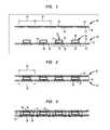
- FIG. 1is a diagrammatic sectional view depicting elements utilized in a process according to one embodiment of the invention.
- FIGS. 2-6are views similar to FIG. 1 , but depicting the elements at progressively later stages of the same process.
- FIG. 7is a diagrammatic sectional view of elements used in a process according to a further embodiment of the invention.
- FIG. 8is a diagrammatic section view depicting elements used in a process according to yet another embodiment of the invention.
- FIG. 9is a view similar to FIGS. 7 and 8 , but depicting elements used in a process according to a further embodiment of the invention.
- FIG. 10is a view depicting the elements shown in FIG. 9 at a later stage of the process.
- FIG. 11is a diagrammatic view depicting a substrate and lead frame utilized in a process according to a further embodiment of the invention.
- FIG. 12is a view depicting the substrate and lead frame of FIG. 11 at a later stage in the process.
- FIG. 13is a diagrammatic sectional view depicting the elements shown in FIGS. 11 and 12 during a still later stage of the process.
- FIG. 14is a diagrammatic sectional view depicting an assembly made using the elements of FIGS. 11-13 .
- An assembly method in accordance with one embodiment of the inventionutilizes a substrate referred to herein for purposes of convenience as the lower substrate 20 incorporating a dielectric layer 21 defining an upper surface 22 and a lower surface 24 .
- the lower substrate 20typically is in the form of a continuous or semicontinuous tape or sheet having a large number of regions 26 . As explained below, each region 26 will constitute a portion of an individual package at the end of the process, and each region 26 includes the features which, as discussed below, will form a part of a single package.
- Dielectric layer 21may be a single layer, or may be a laminate including several sublayers.
- the dielectric layerdesirably is formed primarily from polymeric dielectrics such as polyimide, BT resin, epoxy or other dielectric polymers, and may include reinforcing fibers as, for example, glass fibers.
- Dielectric layer 21may be flexible or rigid.
- Lower substrate 20includes mounting terminals 28 , and later interconnect terminals 29 , exposed at the lower surface 24 of the dielectric layer and conductive connection elements 30 exposed at the upper surface 22 .
- terminals 28 and 29are formed in a layer separate from connection elements 30 , these layers being separated from one another by dielectric layer 21 and electrically connected to one another by conductive elements such as vias 32 extending through the dielectric layer.
- conductive elementssuch as vias 32 extending through the dielectric layer.
- lower substrate 20can be formed as a single metal structure with a single metal layer constituting conductive connection elements 30 as well as terminals 28 and 29 .
- such a layermay be disposed on the bottom surface 24 of the dielectric layer, with the conductive connection elements 30 exposed at the top surface 22 through holes (not shown) in the dielectric layer.
- such a single metal layermay be disposed on the upper surface 22 , with the terminals 28 and 29 being exposed at the lower surface 24 through holes (not shown) in the dielectric layer.
- one or more metallic layers constituting the conductive mounting elements, the terminals or bothcan be disposed within the thickness of the dielectric layer and exposed through holes to the appropriate surfaces.
- Lower substrate 20has apertures 34 extending through the dielectric layer, from the upper surface to the lower surface. Apertures 34 may be in the form of individual holes or elongated slots. Apertures 34 are disposed in the vicinity of interlayer connection terminals 29 . Microelectronic elements 36 are mounted on the upper surface 22 of lower substrate 20 . Each region 26 has one or more of the microelectronic elements mounted thereon. In the particular embodiment illustrate, each region 26 of the lower substrate bears one microelectronic element.
- each microelectronic element 36may be a packaged microelectronic element incorporating a package substrate (not shown) with terminals thereon, these terminals being connected to the conductive connection elements 30 on the lower substrate.
- techniquessuch as anisotropic conductive adhesives can be employed.
- An overmolding 38covers the exposed surfaces of each microelectronic element 36 . In other embodiments, overmolding 38 is omitted.
- microelectronic element 36 within each region 26 of the lower substrateis electrically connected through the conductive connection elements 30 of that region to at least some of the mounting terminals 28 of the same region, to at least some of the interlayer connection terminals 29 of that region or both.
- Microelectronic elements 36may be mounted on the lower substrate using conventional techniques, either as part of the assembly process described herein or in a separate operation used to prepare the lower substrate 20 .
- the process according to this embodiment of the inventionalso uses an upper substrate 40 including a dielectric layer 41 , which may be formed from the same materials as discussed above in connection with the lower dielectric layer, defining an upper surface 42 and a lower surface 44 .
- the upper substratehas layer interlayer connection terminals 49 exposed at lower surface 44 , and conductive mounting terminals 50 exposed at the upper surface.
- these featuresare shown as a two-layer structure, but can be formed from a single layer or multiple layers with the features exposed to one or both of the surfaces through holes in the dielectric layer.
- the upper substrate 40also has a plurality of regions 46 , each such region including a set of interlayer connection terminals 49 and a set of mounting terminals 50 , at least some mounting terminals 50 electrically connected to at least some interlayer connection terminals 49 of the same region.
- lower substrate 20 with microelectronic elements 36 thereonis united with upper substrate 40 , so that the lower surface 44 of the upper substrate 40 rests on the microelectronic elements 36 and faces toward the lower substrate.
- the microelectronic elements 36are positioned between the substrates.
- An adhesive 52may be applied on the lower surface 44 of the upper substrate on the surfaces of microelectronic elements 36 remote from the lower substrate, which surfaces may be the surfaces defined by the encapsulant 38 surrounding each microelectronic element.
- the process of assembling the substrates to one anothermost preferably is conducted while both substrates remain in the form of large substrates incorporating plural regions 26 and 46 .
- the substratesmay be advanced through a pair of nip rollers or through a press, so as to bring the upper substrate into engagement with the surfaces of microelectronic elements 36 on the lower substrate.
- the assembly processmay be conducted simply by laying one sheet onto the other sheet, so as to assemble the substrate with one another. The substrates are assembled with one another so that each region 46 of the upper substrate 20 is aligned with a corresponding region 26 of the lower substrate 20 .
- the layer interconnect terminals 29 in each region of the lower substrateare connected to the layer interconnect terminals 49 of the corresponding region on the upper substrate. This connection is made by applying wire bonds 53 between the layer interconnect terminals. The wire bonds extend through the apertures 34 in the lower substrate. After wire-bonding, at least some of the lower mounting terminals 28 , or at least some contacts on the chip 36 associated with each lower region, are connected to at least some of the mounting terminals 50 on the corresponding region of the upper substrate through the wire bonds and layer interconnect terminals.
- an encapsulant 54is introduced between the lower substrate 20 and upper substrate 40 ( FIG. 4 ).
- the encapsulantmay be any flowable encapsulant compatible with the materials of construction.
- the encapsulant 54is a settable material which, in an uncured state, is a liquid having a relatively low viscosity, and which can be cured to a solid or semisolid condition. Examples of such materials include epoxies, silicones and other materials commonly employed as encapsulants in microelectronic packages. These materials cure by chemical reaction, typically promoted by application of heat. Other encapsulants such as thermoplastic materials which liquify upon heating, and cure to a solid condition by cooling, can be used.
- the encapsulantcan be injected between the substrates by any suitable process. During injection of the encapsulant, some encapsulant may escape through the apertures 34 ( FIG. 3 ) in the lower substrate.
- the substratesmay be constrained between elements of a mold or other fixture during injection of the encapsulant, and these elements may seal the openings 34 in the upper substrate.
- the openings 34 in the lower substratemay be covered by dielectric film such as a solder mask applied over the openings after wire-bonding.
- dielectric filmsuch as a solder mask applied over the openings after wire-bonding.
- the encapsulant injection stepdesirably is also performed while the substrates 40 and 20 remain in their original form, with the various regions of each substrate remaining connected to one another at this stage.
- the encapsulantsurrounds the wire bonds 53 ( FIG. 3 ) and desirably substantially or completely fills the space between the upper and lower substrate, other than the spaces occupied by the microelectronic elements themselves.
- one or more additional microelectronic elements 56are mounted on the exposed top surface 42 of upper substrate 40 , and electrically connected to the mounting terminals 50 of the upper substrate.
- the microelectronic elements 56are mounted to the various regions 46 of the upper substrate. Electrically conductive bonding materials such as solder balls 58 may be applied on the mounting terminals 28 of the lower substrate.
- the additional microelectronic elements 56may be “bare” or unpackaged semiconductor chips or other microelectronic elements, or may be packaged microelectronic elements such as packaged semiconductor chips. In the embodiments depicted, each additional microelectronic element is mounted by directly bonding contacts on the microelectronic element to the mounting elements 50 of the upper substrate.
- the additional microelectronic element 56may be mounted in a “face-up” disposition on the upper substrate and connected by wire bonds to the mounting elements 50 .
- an encapsulant or other covermay be applied over the additional microelectronic elements.
- each such unitincludes one region 26 of the lower substrate and the corresponding region 46 of the upper substrate, together with the microelectronic 36 on the lower substrate and additional microelectronic element 56 on the upper substrate.
- Each such unitis a self-contained stacked package.
- Each unit 60forms a complete stacked package, with one or more additional microelectronic elements 56 connected to one or more microelectronic elements 36 .
- Such a packagecan be mounted on a circuit board or other larger substrate in substantially the same way as a conventional single element microelectronic package.
- the additional microelectronic elements 56 , connective bonding materials 58 or bothcan be mounted to the substrates after severance.
- the assembled substrates or microelectronic elements 36 , with or without the bonding materials 58 , in either the unsevered condition or as separate, severed units,can be handled, shipped and stocked as semifinished articles of commerce.
- Such an arrangementcan be used, for example, where the same microelectronic elements 36 are to be incorporated into a large number of packages, but different additional elements 56 are used in different ones of the packages.
- the encapsulant 54may be omitted.
- the microelectronic elements 36 disposed between the substratesprovide structural support. Additional structural support may be provided between the substrates by providing spacers extending between the dielectric elements at locations not occupied by microelectronic elements 36 or wire bonds 53 .
- a process according to a further embodiment of the inventionuses a lower substrate 120 and upper substrate 140 similar to those discussed above with reference to FIGS. 1-6 .
- the microelectronic elements 136 mounted on lower substrate 120are mounted in “face-up” disposition, without overmolding.
- the contacts on the microelectronic elements 136are electrically connected to the conductive mounting elements 130 on the upper surface of lower substrate 120 by wire bonds 102 before assembly of the upper substrate 140 .
- Spacers 104are provided on the upwardly facing surfaces of microelectronic elements 136 or on the lower face of upper substrate 140 , so as to hold the upper substrate above wire bonds 102 .
- Spacers 104desirably are formed from a dielectric material, and may include or consist of an adhesive layer.
- interlayer connection terminals 129 of the lower substrateare connected to the interlayer connection pads 149 of the upper substrate by wire bonds 152 .
- wire bonds 152After wire-bonding, the assembly shown in FIG. 7 can be processed and handled in the same manner as discussed above with reference to FIGS. 4-6 .
- a process according to yet another embodiment of the inventionagain utilizes a lower substrate 220 and upper substrate 240 similar to those discussed above.
- Microelectronic elements 236are mounted on the upper surface 222 of the lower substrate 220 . Desirably, these microelectronic elements are covered by overmolding 238 around each microelectronic element.
- the microelectronic elements 236may be packaged or unpacked elements.
- the interlayer connection terminals 229 of the lower substrateare exposed at the upper surface 222 of the substrate, whereas the interlayer connection terminals 249 of the upper substrate are exposed at the lower surface 244 of the upper substrate.
- electrically conductive spacing elementssuch as solder balls are positioned between the substrates on interlayer connection terminals, 229 of the lower substrate or 249 of the upper substrate.
- the conductive elementsengage the interlayer connection terminals on the opposite substrate and are bonded thereto.
- Conductive elements 202thus, provide both electrical connection between the substrates and physical spacing between the substrates.
- Additional microelectronic elements 256may be mounted on the upper substrate before or after assembly. As in the other embodiments discussed above, the assembly steps serves to interconnect numerous regions of the upper substrate with numerous regions of the lower substrate in a single operation. As in the embodiments discussed above, the interconnected substrates can be severed so as to form individual units.
- an encapsulant(not shown) optionally may be injected between the substrates in the manner discussed above, desirably before severing the substrates.
- the microelectronic elements 336 on the lower substrate 320are unencapsulated “bare” semiconductor chips. These chips are wire-bonded to the conductive mounting components 330 of the lower substrate using wire bonds 302 similar to the wire bonds discussed above with reference to FIG. 7 .
- the upper substrate 340is assembled to the lower substrate and connected to the lower substrate by conductive elements 304 similar to those discussed above with reference to FIG. 8 .
- an encapsulant 354( FIG. 10 ) is injected between the substrates prior to severing the substrates to form individual units.
- Conductive elements other than solder ballsmay be employed in the various embodiments.
- metallic conductive elements in the form of elongated bumps or pinsmay be used as inter-unit connections in a stack package.
- Pins of these and other typescan be used in the assemblies discussed above.
- One or both of the substratesmay be provided with these pins prior to assembly, so that the pins are engaged with interlayer connection terminals on the opposite substrate.
- a process according to yet another embodiment of the inventionutilizes an upper substrate 440 in the form of a single metal tape incorporating a dielectric layer 421 with upper mounting terminals 450 and interlayer connection terminals 449 defined by a single layer of metallic features on the lower surface of the tape, the mounting 450 being exposed through holes 451 in the dielectric layer to upper surface 422 of the upper substrate.
- a lead frame including numerous leads 452is attached to upper substrate 440 so that each lead 452 extends from one of the interlayer connection terminals 449 , as seen in FIG. 12 . Although only two leads 452 are depicted in the drawings, it should be appreciated that the lead frame includes numerous leads, and may also include a bus bar or other elements to hold the leads in position relative to one another.
- Bus bars or other retaining elementsmay be removed after assembly of the lead frame with the upper substrate.
- a lead frame of the type taught in co-pending, commonly assigned U.S. patent application Ser. No. 10/746,810, filed Dec. 24, 2003, the disclosure of which is hereby incorporated by reference herein,may be utilized.
- the lead framemay be bonded to the interlayer connection terminals 449 of the upper substrate by processes such as solder-bonding, diffusion-bonding, thermocompression-bonding or the like.
- interlayer connection terminals 449may be made in the form of tape-automated bonding (“TAB”) leads, and these leads may be bonded to the lead frame using processes similar to those commonly used to bond TAB leads to elements such as semiconductor chips. As best seen in FIG.
- TABtape-automated bonding
- the leads 452 of the lead frameproject downwardly from the upper substrate 440 .
- the processalso utilizes a lower substrate 420 which has lower mounting terminals 428 exposed at its lower surface 424 , and has electrical connections 430 exposed at its upper surface and interlayer connection terminals 429 also exposed at its upper surface 422 .
- the lower substrateis shown as a “two-metal” structure, but could be a single metal structure with various features exposed through holes in the dielectric element 421 of the lower substrate.
- a semiconductor chip or other microelectronic element 436is mounted to lower substrate 420 .
- the semiconductor chip 436is mounted in face-up disposition and connected by wire bonds 402 to the connection terminals 430 .
- chip 436could also be mounted face-down.
- chip 436could be a packaged chip or other packaged microelectronic element.
- chip 436is supported above the dielectric element 421 of the lower substrate by a spacer 404 .
- spacer 404could be replaced by a further semiconductor chip or other microelectronic element which may be mounted face-up or face-down.
- a spacer 406desirably formed from a dielectric material, is disposed on the surface of microelectronic element 436 remote from lower substrate 420 .
- the subassembly including the upper substrate 440 and leads 452 of the lead frameis mounted to the lower substrate by advancing the subassembly toward the lower substrate and bonding the lower ends of leads 452 , remote from upper substrate 441 to the interlayer connection terminals 429 of the lower substrate using any of the techniques discussed above.
- the resulting unitincluding lower substrate 420 , upper substrate 440 , microelectronic element 436 and leads 452 connecting the upper and lower substrates, is encapsulated as, for example, by introducing a flowable encapsulant around the microelectronic element 436 and between substrates 420 and 440 .
- the encapsulation processis conducted so as to leave upper mounting terminals 450 and lower mounting terminals 428 exposed and uncovered by the encapsulant 454 .
- All of the steps discussed above with reference to FIGS. 11-14may be conducted using individual upper and lower substrates and/or individual lead frames, or may be conducted while the upper substrate, the lower substrate, the lead frames or any combination of these are in the form of larger assemblies such as tapes or strips incorporating numerous substrates and/or numerous lead frames.
- the larger elementsare severed as discussed above, so as to form individual units, each including a lower substrate, an upper substrate and one or more microelectronic elements 436 .
- the larger units, before severancecan be handled, shipped and stocked as an article of commerce.
- a packaged or unpackaged additional microelectronic element 456may be mounted to the upper mounting terminal as, for example, by solder-bonding, as seen in FIG. 14 , or by wire-bonding.
- the lower mounting terminals 428may be provided with electrically conductive bonding material such as solder balls 408 and may be used to mount the finished assembly to a circuit panel.
- the roles of the upper and lower substratesmay be reversed.
- the upper mounting terminals 450 of the assembly seen in FIG. 14may be used to mount the assembly to a circuit panel, whereas the lower mounting terminals 428 may be used to mount a further microelectronic element to the assembly.
- the leads 452 of the lead framemay be assembled to the lower substrate rather than the upper substrate.
- the entire upper substratemay consist solely of elements from a lead frame.
- the bus bars or other parts of the lead frame which serve to interconnect the various leads and form a self-supporting lead framemay be removed after encapsulation.
- the lower substrate 420may be replaced by elements of the lead frame.
- the ends of the lead frame remote from the upper substrateare exposed so that these ends serve as the lower mounting terminals of the assembly.
Landscapes
- Engineering & Computer Science (AREA)
- Microelectronics & Electronic Packaging (AREA)
- Power Engineering (AREA)
- Computer Hardware Design (AREA)
- Physics & Mathematics (AREA)
- Condensed Matter Physics & Semiconductors (AREA)
- General Physics & Mathematics (AREA)
- Manufacturing & Machinery (AREA)
- Combinations Of Printed Boards (AREA)
- Encapsulation Of And Coatings For Semiconductor Or Solid State Devices (AREA)
- Production Of Multi-Layered Print Wiring Board (AREA)
- Semiconductor Integrated Circuits (AREA)
Abstract
Description
Claims (7)
Priority Applications (1)
| Application Number | Priority Date | Filing Date | Title |
|---|---|---|---|
| US12/938,094US8531020B2 (en) | 2004-11-03 | 2010-11-02 | Stacked packaging improvements |
Applications Claiming Priority (4)
| Application Number | Priority Date | Filing Date | Title |
|---|---|---|---|
| US62466704P | 2004-11-03 | 2004-11-03 | |
| PCT/US2005/039716WO2006052616A1 (en) | 2004-11-03 | 2005-11-03 | Stacked packaging improvements |
| US11/666,975US8525314B2 (en) | 2004-11-03 | 2005-11-03 | Stacked packaging improvements |
| US12/938,094US8531020B2 (en) | 2004-11-03 | 2010-11-02 | Stacked packaging improvements |
Related Parent Applications (3)
| Application Number | Title | Priority Date | Filing Date |
|---|---|---|---|
| US11/666,975ContinuationUS8525314B2 (en) | 2004-11-03 | 2005-11-03 | Stacked packaging improvements |
| PCT/US2005/039716ContinuationWO2006052616A1 (en) | 2004-11-03 | 2005-11-03 | Stacked packaging improvements |
| US12/666,975ContinuationUS20100196539A1 (en) | 2007-06-25 | 2008-06-23 | Novel prebiotics |
Publications (2)
| Publication Number | Publication Date |
|---|---|
| US20110042810A1 US20110042810A1 (en) | 2011-02-24 |
| US8531020B2true US8531020B2 (en) | 2013-09-10 |
Family
ID=36061305
Family Applications (5)
| Application Number | Title | Priority Date | Filing Date |
|---|---|---|---|
| US11/666,975Expired - Fee RelatedUS8525314B2 (en) | 2004-11-03 | 2005-11-03 | Stacked packaging improvements |
| US12/938,094Expired - Fee RelatedUS8531020B2 (en) | 2004-11-03 | 2010-11-02 | Stacked packaging improvements |
| US14/011,086ActiveUS8927337B2 (en) | 2004-11-03 | 2013-08-27 | Stacked packaging improvements |
| US14/574,988ActiveUS9153562B2 (en) | 2004-11-03 | 2014-12-18 | Stacked packaging improvements |
| US14/870,827ActiveUS9570416B2 (en) | 2004-11-03 | 2015-09-30 | Stacked packaging improvements |
Family Applications Before (1)
| Application Number | Title | Priority Date | Filing Date |
|---|---|---|---|
| US11/666,975Expired - Fee RelatedUS8525314B2 (en) | 2004-11-03 | 2005-11-03 | Stacked packaging improvements |
Family Applications After (3)
| Application Number | Title | Priority Date | Filing Date |
|---|---|---|---|
| US14/011,086ActiveUS8927337B2 (en) | 2004-11-03 | 2013-08-27 | Stacked packaging improvements |
| US14/574,988ActiveUS9153562B2 (en) | 2004-11-03 | 2014-12-18 | Stacked packaging improvements |
| US14/870,827ActiveUS9570416B2 (en) | 2004-11-03 | 2015-09-30 | Stacked packaging improvements |
Country Status (5)
| Country | Link |
|---|---|
| US (5) | US8525314B2 (en) |
| JP (2) | JP5592055B2 (en) |
| KR (1) | KR101313391B1 (en) |
| CN (1) | CN101053079A (en) |
| WO (1) | WO2006052616A1 (en) |
Cited By (1)
| Publication number | Priority date | Publication date | Assignee | Title |
|---|---|---|---|---|
| US10424525B2 (en) | 2017-05-23 | 2019-09-24 | Stmicroelectronics S.R.L. | Method of manufacturing semiconductor devices |
Families Citing this family (63)
| Publication number | Priority date | Publication date | Assignee | Title |
|---|---|---|---|---|
| KR101313391B1 (en) | 2004-11-03 | 2013-10-01 | 테세라, 인코포레이티드 | Stacked packaging improvements |
| JPWO2007069606A1 (en) | 2005-12-14 | 2009-05-21 | 新光電気工業株式会社 | Manufacturing method of chip embedded substrate |
| US8058101B2 (en) | 2005-12-23 | 2011-11-15 | Tessera, Inc. | Microelectronic packages and methods therefor |
| US8129225B2 (en)* | 2007-08-10 | 2012-03-06 | Infineon Technologies Ag | Method of manufacturing an integrated circuit module |
| KR100913722B1 (en) | 2008-02-13 | 2009-08-24 | 전자부품연구원 | Multi chip package and manufacturing method thereof |
| US20100187651A1 (en) | 2009-01-26 | 2010-07-29 | Stmicroelectronics Asia Pacific Pte Ltd. | Integrated circuit package and method of forming the same |
| EP2290683A1 (en)* | 2009-08-27 | 2011-03-02 | ABB Research Ltd | Wiring of an electronic module |
| US9159708B2 (en) | 2010-07-19 | 2015-10-13 | Tessera, Inc. | Stackable molded microelectronic packages with area array unit connectors |
| US8482111B2 (en) | 2010-07-19 | 2013-07-09 | Tessera, Inc. | Stackable molded microelectronic packages |
| KR101075241B1 (en) | 2010-11-15 | 2011-11-01 | 테세라, 인코포레이티드 | Microelectronic package with terminals in dielectric member |
| US20120146206A1 (en) | 2010-12-13 | 2012-06-14 | Tessera Research Llc | Pin attachment |
| KR101128063B1 (en) | 2011-05-03 | 2012-04-23 | 테세라, 인코포레이티드 | Package-on-package assembly with wire bonds to encapsulation surface |
| US11830845B2 (en)* | 2011-05-03 | 2023-11-28 | Tessera Llc | Package-on-package assembly with wire bonds to encapsulation surface |
| US8618659B2 (en) | 2011-05-03 | 2013-12-31 | Tessera, Inc. | Package-on-package assembly with wire bonds to encapsulation surface |
| US8872318B2 (en) | 2011-08-24 | 2014-10-28 | Tessera, Inc. | Through interposer wire bond using low CTE interposer with coarse slot apertures |
| US8836136B2 (en) | 2011-10-17 | 2014-09-16 | Invensas Corporation | Package-on-package assembly with wire bond vias |
| US8680684B2 (en) | 2012-01-09 | 2014-03-25 | Invensas Corporation | Stackable microelectronic package structures |
| US8946757B2 (en) | 2012-02-17 | 2015-02-03 | Invensas Corporation | Heat spreading substrate with embedded interconnects |
| US8372741B1 (en) | 2012-02-24 | 2013-02-12 | Invensas Corporation | Method for package-on-package assembly with wire bonds to encapsulation surface |
| US9349706B2 (en) | 2012-02-24 | 2016-05-24 | Invensas Corporation | Method for package-on-package assembly with wire bonds to encapsulation surface |
| US8835228B2 (en) | 2012-05-22 | 2014-09-16 | Invensas Corporation | Substrate-less stackable package with wire-bond interconnect |
| US9391008B2 (en) | 2012-07-31 | 2016-07-12 | Invensas Corporation | Reconstituted wafer-level package DRAM |
| US9502390B2 (en) | 2012-08-03 | 2016-11-22 | Invensas Corporation | BVA interposer |
| US8975738B2 (en) | 2012-11-12 | 2015-03-10 | Invensas Corporation | Structure for microelectronic packaging with terminals on dielectric mass |
| US8878353B2 (en) | 2012-12-20 | 2014-11-04 | Invensas Corporation | Structure for microelectronic packaging with bond elements to encapsulation surface |
| US9136254B2 (en) | 2013-02-01 | 2015-09-15 | Invensas Corporation | Microelectronic package having wire bond vias and stiffening layer |
| US8970023B2 (en) | 2013-02-04 | 2015-03-03 | Taiwan Semiconductor Manufacturing Company, Ltd. | Package structure and methods of forming same |
| US9023691B2 (en) | 2013-07-15 | 2015-05-05 | Invensas Corporation | Microelectronic assemblies with stack terminals coupled by connectors extending through encapsulation |
| US8883563B1 (en) | 2013-07-15 | 2014-11-11 | Invensas Corporation | Fabrication of microelectronic assemblies having stack terminals coupled by connectors extending through encapsulation |
| US9034696B2 (en) | 2013-07-15 | 2015-05-19 | Invensas Corporation | Microelectronic assemblies having reinforcing collars on connectors extending through encapsulation |
| US9167710B2 (en) | 2013-08-07 | 2015-10-20 | Invensas Corporation | Embedded packaging with preformed vias |
| US9685365B2 (en) | 2013-08-08 | 2017-06-20 | Invensas Corporation | Method of forming a wire bond having a free end |
| US20150076714A1 (en) | 2013-09-16 | 2015-03-19 | Invensas Corporation | Microelectronic element with bond elements to encapsulation surface |
| US9087815B2 (en) | 2013-11-12 | 2015-07-21 | Invensas Corporation | Off substrate kinking of bond wire |
| US9082753B2 (en) | 2013-11-12 | 2015-07-14 | Invensas Corporation | Severing bond wire by kinking and twisting |
| US9263394B2 (en) | 2013-11-22 | 2016-02-16 | Invensas Corporation | Multiple bond via arrays of different wire heights on a same substrate |
| US9379074B2 (en) | 2013-11-22 | 2016-06-28 | Invensas Corporation | Die stacks with one or more bond via arrays of wire bond wires and with one or more arrays of bump interconnects |
| US9583456B2 (en) | 2013-11-22 | 2017-02-28 | Invensas Corporation | Multiple bond via arrays of different wire heights on a same substrate |
| US9583411B2 (en) | 2014-01-17 | 2017-02-28 | Invensas Corporation | Fine pitch BVA using reconstituted wafer with area array accessible for testing |
| US9653442B2 (en)* | 2014-01-17 | 2017-05-16 | Taiwan Semiconductor Manufacturing Company, Ltd. | Integrated circuit package and methods of forming same |
| US9214454B2 (en) | 2014-03-31 | 2015-12-15 | Invensas Corporation | Batch process fabrication of package-on-package microelectronic assemblies |
| US10381326B2 (en) | 2014-05-28 | 2019-08-13 | Invensas Corporation | Structure and method for integrated circuits packaging with increased density |
| US9646917B2 (en) | 2014-05-29 | 2017-05-09 | Invensas Corporation | Low CTE component with wire bond interconnects |
| US9412714B2 (en) | 2014-05-30 | 2016-08-09 | Invensas Corporation | Wire bond support structure and microelectronic package including wire bonds therefrom |
| US9735084B2 (en) | 2014-12-11 | 2017-08-15 | Invensas Corporation | Bond via array for thermal conductivity |
| WO2016123607A2 (en) | 2015-01-30 | 2016-08-04 | Invensas Corporation | Contact arrangements for stackable microelectronic package structures |
| US9888579B2 (en) | 2015-03-05 | 2018-02-06 | Invensas Corporation | Pressing of wire bond wire tips to provide bent-over tips |
| KR101605172B1 (en)* | 2015-04-07 | 2016-03-22 | 삼성전자주식회사 | Package substrate and methods for fabricating the same |
| US9502372B1 (en) | 2015-04-30 | 2016-11-22 | Invensas Corporation | Wafer-level packaging using wire bond wires in place of a redistribution layer |
| US9761554B2 (en) | 2015-05-07 | 2017-09-12 | Invensas Corporation | Ball bonding metal wire bond wires to metal pads |
| US10685943B2 (en) | 2015-05-14 | 2020-06-16 | Mediatek Inc. | Semiconductor chip package with resilient conductive paste post and fabrication method thereof |
| US9842831B2 (en) | 2015-05-14 | 2017-12-12 | Mediatek Inc. | Semiconductor package and fabrication method thereof |
| US10490528B2 (en) | 2015-10-12 | 2019-11-26 | Invensas Corporation | Embedded wire bond wires |
| US9490222B1 (en) | 2015-10-12 | 2016-11-08 | Invensas Corporation | Wire bond wires for interference shielding |
| US10332854B2 (en) | 2015-10-23 | 2019-06-25 | Invensas Corporation | Anchoring structure of fine pitch bva |
| US10181457B2 (en) | 2015-10-26 | 2019-01-15 | Invensas Corporation | Microelectronic package for wafer-level chip scale packaging with fan-out |
| US10043779B2 (en) | 2015-11-17 | 2018-08-07 | Invensas Corporation | Packaged microelectronic device for a package-on-package device |
| US9659848B1 (en) | 2015-11-18 | 2017-05-23 | Invensas Corporation | Stiffened wires for offset BVA |
| US9984992B2 (en) | 2015-12-30 | 2018-05-29 | Invensas Corporation | Embedded wire bond wires for vertical integration with separate surface mount and wire bond mounting surfaces |
| CN106205161B (en)* | 2016-07-09 | 2018-09-18 | 腾讯科技(深圳)有限公司 | traffic information transmission method and device |
| US9935075B2 (en) | 2016-07-29 | 2018-04-03 | Invensas Corporation | Wire bonding method and apparatus for electromagnetic interference shielding |
| US10299368B2 (en) | 2016-12-21 | 2019-05-21 | Invensas Corporation | Surface integrated waveguides and circuit structures therefor |
| US10410999B2 (en)* | 2017-12-19 | 2019-09-10 | Amkor Technology, Inc. | Semiconductor device with integrated heat distribution and manufacturing method thereof |
Citations (282)
| Publication number | Priority date | Publication date | Assignee | Title |
|---|---|---|---|---|
| US3358897A (en) | 1964-03-31 | 1967-12-19 | Tempress Res Co | Electric lead wire bonding tools |
| US3623649A (en) | 1969-06-09 | 1971-11-30 | Gen Motors Corp | Wedge bonding tool for the attachment of semiconductor leads |
| US3795037A (en) | 1970-05-05 | 1974-03-05 | Int Computers Ltd | Electrical connector devices |
| US3900153A (en) | 1972-06-13 | 1975-08-19 | Licentia Gmbh | Formation of solder layers |
| US4327860A (en) | 1980-01-03 | 1982-05-04 | Kulicke And Soffa Ind. Inc. | Method of making slack free wire interconnections |
| US4422568A (en) | 1981-01-12 | 1983-12-27 | Kulicke And Soffa Industries, Inc. | Method of making constant bonding wire tail lengths |
| US4437604A (en) | 1982-03-15 | 1984-03-20 | Kulicke & Soffa Industries, Inc. | Method of making fine wire interconnections |
| US4604644A (en) | 1985-01-28 | 1986-08-05 | International Business Machines Corporation | Solder interconnection structure for joining semiconductor devices to substrates that have improved fatigue life, and process for making |
| US4695870A (en) | 1986-03-27 | 1987-09-22 | Hughes Aircraft Company | Inverted chip carrier |
| US4716049A (en) | 1985-12-20 | 1987-12-29 | Hughes Aircraft Company | Compressive pedestal for microminiature connections |
| US4771930A (en) | 1986-06-30 | 1988-09-20 | Kulicke And Soffa Industries Inc. | Apparatus for supplying uniform tail lengths |
| US4793814A (en) | 1986-07-21 | 1988-12-27 | Rogers Corporation | Electrical circuit board interconnect |
| US4804132A (en) | 1987-08-28 | 1989-02-14 | Difrancesco Louis | Method for cold bonding |
| US4902600A (en) | 1986-10-14 | 1990-02-20 | Fuji Photo Film Co., Ltd. | Light-sensitive material comprising light-sensitive layer provided on support wherein the light-sensitive layer and support have specified pH values |
| US4924353A (en) | 1985-12-20 | 1990-05-08 | Hughes Aircraft Company | Connector system for coupling to an integrated circuit chip |
| US4975079A (en) | 1990-02-23 | 1990-12-04 | International Business Machines Corp. | Connector assembly for chip testing |
| US4982265A (en) | 1987-06-24 | 1991-01-01 | Hitachi, Ltd. | Semiconductor integrated circuit device and method of manufacturing the same |
| US4998885A (en) | 1989-10-27 | 1991-03-12 | International Business Machines Corporation | Elastomeric area array interposer |
| US4999472A (en) | 1990-03-12 | 1991-03-12 | Neinast James E | Electric arc system for ablating a surface coating |
| US5083697A (en) | 1990-02-14 | 1992-01-28 | Difrancesco Louis | Particle-enhanced joining of metal surfaces |
| US5138438A (en) | 1987-06-24 | 1992-08-11 | Akita Electronics Co. Ltd. | Lead connections means for stacked tab packaged IC chips |
| US5148265A (en) | 1990-09-24 | 1992-09-15 | Ist Associates, Inc. | Semiconductor chip assemblies with fan-in leads |
| US5148266A (en) | 1990-09-24 | 1992-09-15 | Ist Associates, Inc. | Semiconductor chip assemblies having interposer and flexible lead |
| US5186381A (en) | 1991-04-16 | 1993-02-16 | Samsung Electronics, Co., Ltd. | Semiconductor chip bonding process |
| US5189505A (en) | 1989-11-08 | 1993-02-23 | Hewlett-Packard Company | Flexible attachment flip-chip assembly |
| US5196726A (en) | 1990-01-23 | 1993-03-23 | Sumitomo Electric Industries, Ltd. | Substrate for packaging a semiconductor device having particular terminal and bump structure |
| US5214308A (en) | 1990-01-23 | 1993-05-25 | Sumitomo Electric Industries, Ltd. | Substrate for packaging a semiconductor device |
| US5220489A (en) | 1991-10-11 | 1993-06-15 | Motorola, Inc. | Multicomponent integrated circuit package |
| US5222014A (en) | 1992-03-02 | 1993-06-22 | Motorola, Inc. | Three-dimensional multi-chip pad array carrier |
| US5340771A (en) | 1993-03-18 | 1994-08-23 | Lsi Logic Corporation | Techniques for providing high I/O count connections to semiconductor dies |
| US5371654A (en) | 1992-10-19 | 1994-12-06 | International Business Machines Corporation | Three dimensional high performance interconnection package |
| US5397997A (en) | 1991-08-23 | 1995-03-14 | Nchip, Inc. | Burn-in technologies for unpackaged integrated circuits |
| US5438224A (en) | 1992-04-23 | 1995-08-01 | Motorola, Inc. | Integrated circuit package having a face-to-face IC chip arrangement |
| US5455390A (en) | 1994-02-01 | 1995-10-03 | Tessera, Inc. | Microelectronics unit mounting with multiple lead bonding |
| US5494667A (en) | 1992-06-04 | 1996-02-27 | Kabushiki Kaisha Hayahibara | Topically applied hair restorer containing pine extract |
| US5495667A (en) | 1994-11-07 | 1996-03-05 | Micron Technology, Inc. | Method for forming contact pins for semiconductor dice and interconnects |
| US5518964A (en) | 1994-07-07 | 1996-05-21 | Tessera, Inc. | Microelectronic mounting with multiple lead deformation and bonding |
| US5536909A (en) | 1992-07-24 | 1996-07-16 | Tessera, Inc. | Semiconductor connection components and methods with releasable lead support |
| US5541567A (en) | 1994-10-17 | 1996-07-30 | International Business Machines Corporation | Coaxial vias in an electronic substrate |
| US5571428A (en) | 1992-01-17 | 1996-11-05 | Hitachi, Ltd. | Semiconductor leadframe and its production method and plastic encapsulated semiconductor device |
| US5615824A (en) | 1994-06-07 | 1997-04-01 | Tessera, Inc. | Soldering with resilient contacts |
| US5656550A (en) | 1994-08-24 | 1997-08-12 | Fujitsu Limited | Method of producing a semicondutor device having a lead portion with outer connecting terminal |
| US5659952A (en) | 1994-09-20 | 1997-08-26 | Tessera, Inc. | Method of fabricating compliant interface for semiconductor chip |
| US5679977A (en) | 1990-09-24 | 1997-10-21 | Tessera, Inc. | Semiconductor chip assemblies, methods of making same and components for same |
| US5688716A (en) | 1994-07-07 | 1997-11-18 | Tessera, Inc. | Fan-out semiconductor chip assembly |
| US5726493A (en) | 1994-06-13 | 1998-03-10 | Fujitsu Limited | Semiconductor device and semiconductor device unit having ball-grid-array type package structure |
| US5731709A (en) | 1996-01-26 | 1998-03-24 | Motorola, Inc. | Method for testing a ball grid array semiconductor device and a device for such testing |
| US5736780A (en) | 1995-11-07 | 1998-04-07 | Shinko Electric Industries Co., Ltd. | Semiconductor device having circuit pattern along outer periphery of sealing resin and related processes |
| US5802699A (en) | 1994-06-07 | 1998-09-08 | Tessera, Inc. | Methods of assembling microelectronic assembly with socket for engaging bump leads |
| US5811982A (en) | 1995-11-27 | 1998-09-22 | International Business Machines Corporation | High density cantilevered probe for electronic devices |
| US5831836A (en) | 1992-01-30 | 1998-11-03 | Lsi Logic | Power plane for semiconductor device |
| US5854507A (en) | 1998-07-21 | 1998-12-29 | Hewlett-Packard Company | Multiple chip assembly |
| US5898991A (en) | 1997-01-16 | 1999-05-04 | International Business Machines Corporation | Methods of fabrication of coaxial vias and magnetic devices |
| US5912505A (en) | 1995-11-07 | 1999-06-15 | Sumitomo Metal (Smi) Electronics Devices, Inc. | Semiconductor package and semiconductor device |
| US5953624A (en) | 1997-01-13 | 1999-09-14 | Kabushiki Kaisha Shinkawa | Bump forming method |
| US5971253A (en) | 1995-07-31 | 1999-10-26 | Tessera, Inc. | Microelectronic component mounting with deformable shell terminals |
| US5973391A (en) | 1997-12-11 | 1999-10-26 | Read-Rite Corporation | Interposer with embedded circuitry and method for using the same to package microelectronic units |
| US5977618A (en) | 1992-07-24 | 1999-11-02 | Tessera, Inc. | Semiconductor connection components and methods with releasable lead support |
| US5989936A (en) | 1994-07-07 | 1999-11-23 | Tessera, Inc. | Microelectronic assembly fabrication with terminal formation from a conductive layer |
| US5994152A (en) | 1996-02-21 | 1999-11-30 | Formfactor, Inc. | Fabricating interconnects and tips using sacrificial substrates |
| US6002168A (en) | 1997-11-25 | 1999-12-14 | Tessera, Inc. | Microelectronic component with rigid interposer |
| US6032359A (en) | 1997-08-21 | 2000-03-07 | Carroll; Keith C. | Method of manufacturing a female electrical connector in a single layer flexible polymeric dielectric film substrate |
| US6038136A (en) | 1997-10-29 | 2000-03-14 | Hestia Technologies, Inc. | Chip package with molded underfill |
| US6052287A (en) | 1997-12-09 | 2000-04-18 | Sandia Corporation | Silicon ball grid array chip carrier |
| US6054756A (en) | 1992-07-24 | 2000-04-25 | Tessera, Inc. | Connection components with frangible leads and bus |
| US6077380A (en) | 1995-06-30 | 2000-06-20 | Microfab Technologies, Inc. | Method of forming an adhesive connection |
| US6117694A (en) | 1994-07-07 | 2000-09-12 | Tessera, Inc. | Flexible lead structures and methods of making same |
| KR100265563B1 (en) | 1998-06-29 | 2000-09-15 | 김영환 | Ball grid array package and fabricating method thereof |
| US6121676A (en) | 1996-12-13 | 2000-09-19 | Tessera, Inc. | Stacked microelectronic assembly and method therefor |
| US6124546A (en) | 1997-12-03 | 2000-09-26 | Advanced Micro Devices, Inc. | Integrated circuit chip package and method of making the same |
| US6133072A (en) | 1996-12-13 | 2000-10-17 | Tessera, Inc. | Microelectronic connector with planar elastomer sockets |
| US6157080A (en) | 1997-11-06 | 2000-12-05 | Sharp Kabushiki Kaisha | Semiconductor device using a chip scale package |
| US6158647A (en) | 1998-09-29 | 2000-12-12 | Micron Technology, Inc. | Concave face wire bond capillary |
| US6164523A (en) | 1998-07-01 | 2000-12-26 | Semiconductor Components Industries, Llc | Electronic component and method of manufacture |
| US6177636B1 (en) | 1994-12-29 | 2001-01-23 | Tessera, Inc. | Connection components with posts |
| US6194250B1 (en) | 1998-09-14 | 2001-02-27 | Motorola, Inc. | Low-profile microelectronic package |
| US6202297B1 (en) | 1995-08-28 | 2001-03-20 | Tessera, Inc. | Socket for engaging bump leads on a microelectronic device and methods therefor |
| US6206273B1 (en) | 1999-02-17 | 2001-03-27 | International Business Machines Corporation | Structures and processes to create a desired probetip contact geometry on a wafer test probe |
| US6208024B1 (en) | 1996-12-12 | 2001-03-27 | Tessera, Inc. | Microelectronic mounting with multiple lead deformation using restraining straps |
| US6211572B1 (en) | 1995-10-31 | 2001-04-03 | Tessera, Inc. | Semiconductor chip package with fan-in leads |
| US6215670B1 (en) | 1993-11-16 | 2001-04-10 | Formfactor, Inc. | Method for manufacturing raised electrical contact pattern of controlled geometry |
| US6218728B1 (en) | 1997-10-28 | 2001-04-17 | Nec Corporation | Mold-BGA-type semiconductor device and method for making the same |
| US6225688B1 (en) | 1997-12-11 | 2001-05-01 | Tessera, Inc. | Stacked microelectronic assembly and method therefor |
| US20010002607A1 (en) | 1999-12-02 | 2001-06-07 | Kazuo Sugiura | Method for forming pin-form wires and the like |
| US6258625B1 (en) | 1999-05-18 | 2001-07-10 | International Business Machines Corporation | Method of interconnecting electronic components using a plurality of conductive studs |
| US6260264B1 (en) | 1997-12-08 | 2001-07-17 | 3M Innovative Properties Company | Methods for making z-axis electrical connections |
| US6262482B1 (en) | 1998-02-03 | 2001-07-17 | Oki Electric Industry Co., Ltd. | Semiconductor device |
| JP2001196407A (en) | 2000-01-14 | 2001-07-19 | Seiko Instruments Inc | Semiconductor device and method of forming the same |
| US6295729B1 (en) | 1992-10-19 | 2001-10-02 | International Business Machines Corporation | Angled flying lead wire bonding process |
| US20010028114A1 (en) | 2000-03-27 | 2001-10-11 | Kabushiki Kaisha Toshiba | Semiconductor device including memory unit and semiconductor module including memory units |
| US6303997B1 (en) | 1998-04-08 | 2001-10-16 | Anam Semiconductor, Inc. | Thin, stackable semiconductor packages |
| KR20010094894A (en) | 2000-04-07 | 2001-11-03 | 마이클 디. 오브라이언 | Semiconductor package and its manufacturing method |
| US6313528B1 (en) | 1996-12-13 | 2001-11-06 | Tessera, Inc. | Compliant multichip package |
| US6316838B1 (en) | 1999-10-29 | 2001-11-13 | Fujitsu Limited | Semiconductor device |
| US6332270B2 (en) | 1998-11-23 | 2001-12-25 | International Business Machines Corporation | Method of making high density integral test probe |
| WO2002013256A1 (en) | 2000-08-08 | 2002-02-14 | Telefonaktiebolaget Lm Ericsson (Publ) | Method of securing solder balls and any components fixed to one and the same side of a substrate |
| US6358627B2 (en) | 1999-04-03 | 2002-03-19 | International Business Machines Corporation | Rolling ball connector |
| US6362525B1 (en) | 1999-11-09 | 2002-03-26 | Cypress Semiconductor Corp. | Circuit structure including a passive element formed within a grid array substrate and method for making the same |
| US6388333B1 (en) | 1999-11-30 | 2002-05-14 | Fujitsu Limited | Semiconductor device having protruding electrodes higher than a sealed portion |
| US20020066952A1 (en) | 2000-12-04 | 2002-06-06 | Fujitsu Limited | Semiconductor device having an interconnecting post formed on an interposer within a sealing resin |
| US6407448B2 (en) | 1998-05-30 | 2002-06-18 | Hyundai Electronics Industries Co., Inc. | Stackable ball grid array semiconductor package and fabrication method thereof |
| KR20020058216A (en) | 2000-12-29 | 2002-07-12 | 마이클 디. 오브라이언 | Stacked semiconductor package and its manufacturing method |
| US20020117330A1 (en) | 1993-11-16 | 2002-08-29 | Formfactor, Inc. | Resilient contact structures formed and then attached to a substrate |
| US20020125571A1 (en) | 1998-06-30 | 2002-09-12 | Corisis David J. | Module assembly for stacked BGA packages |
| US6458411B1 (en) | 2001-01-17 | 2002-10-01 | Aralight, Inc. | Method of making a mechanically compliant bump |
| US20020153602A1 (en) | 2000-05-16 | 2002-10-24 | Tay Wuu Yean | Ball grid array chip packages having improved testing and stacking characteristics |
| US20020164838A1 (en) | 2001-05-02 | 2002-11-07 | Moon Ow Chee | Flexible ball grid array chip scale packages and methods of fabrication |
| US20020185735A1 (en) | 1998-10-28 | 2002-12-12 | International Business Machines Corporation | Bump connection and method and apparatus for forming said connection |
| US6495914B1 (en) | 1997-08-19 | 2002-12-17 | Hitachi, Ltd. | Multi-chip module structure having conductive blocks to provide electrical connection between conductors on first and second sides of a conductive base substrate |
| US20030006494A1 (en)* | 2001-07-03 | 2003-01-09 | Lee Sang Ho | Thin profile stackable semiconductor package and method for manufacturing |
| US6507104B2 (en) | 2000-09-07 | 2003-01-14 | Siliconware Precision Industries Co., Ltd. | Semiconductor package with embedded heat-dissipating device |
| US6515355B1 (en) | 1998-09-02 | 2003-02-04 | Micron Technology, Inc. | Passivation layer for packaged integrated circuits |
| US6514847B1 (en) | 1997-11-28 | 2003-02-04 | Sony Corporation | Method for making a semiconductor device |
| US6531784B1 (en) | 2000-06-02 | 2003-03-11 | Amkor Technology, Inc. | Semiconductor package with spacer strips |
| US20030048108A1 (en) | 1993-04-30 | 2003-03-13 | Beaman Brian Samuel | Structural design and processes to control probe position accuracy in a wafer test probe assembly |
| US20030057544A1 (en) | 2001-09-13 | 2003-03-27 | Nathan Richard J. | Integrated assembly protocol |
| US6545228B2 (en) | 2000-09-05 | 2003-04-08 | Seiko Epson Corporation | Semiconductor device with a plurality of stacked boards and method of making |
| US6550666B2 (en) | 2001-08-21 | 2003-04-22 | Advanpack Solutions Pte Ltd | Method for forming a flip chip on leadframe semiconductor package |
| JP2003122611A (en) | 2001-10-11 | 2003-04-25 | Oki Electric Ind Co Ltd | Data providing method and server device |
| US6555918B2 (en) | 1997-09-29 | 2003-04-29 | Hitachi, Ltd. | Stacked semiconductor device including improved lead frame arrangement |
| US6560117B2 (en) | 2000-06-28 | 2003-05-06 | Micron Technology, Inc. | Packaged microelectronic die assemblies and methods of manufacture |
| US6573458B1 (en) | 1998-09-07 | 2003-06-03 | Ngk Spark Plug Co., Ltd. | Printed circuit board |
| US6578754B1 (en) | 2000-04-27 | 2003-06-17 | Advanpack Solutions Pte. Ltd. | Pillar connections for semiconductor chips and method of manufacture |
| JP2003174124A (en) | 2001-12-04 | 2003-06-20 | Sainekkusu:Kk | Method for forming external electrode of semiconductor device |
| US20030124767A1 (en) | 2001-12-31 | 2003-07-03 | Jin-Yuan Lee | Integrated chip package structure using ceramic substrate and method of manufacturing the same |
| US20030162378A1 (en) | 2001-12-28 | 2003-08-28 | Seiko Epson Corporation | Bonding method and bonding apparatus |
| US20030164540A1 (en) | 2002-03-04 | 2003-09-04 | Lee Teck Kheng | Semiconductor die packages with recessed interconnecting structures and methods for assembling the same |
| US6624653B1 (en) | 2000-08-28 | 2003-09-23 | Micron Technology, Inc. | Method and system for wafer level testing and burning-in semiconductor components |
| US6630730B2 (en) | 2000-04-28 | 2003-10-07 | Micron Technology, Inc. | Semiconductor device assemblies including interposers with dams protruding therefrom |
| JP2003307897A (en) | 2001-10-16 | 2003-10-31 | Hokushin Ind Inc | Conductive blade |
| US6647310B1 (en) | 2000-05-30 | 2003-11-11 | Advanced Micro Devices, Inc. | Temperature control of an integrated circuit |
| US6684007B2 (en) | 1998-10-09 | 2004-01-27 | Fujitsu Limited | Optical coupling structures and the fabrication processes |
| US6687988B1 (en) | 1999-10-20 | 2004-02-10 | Kabushiki Kaisha Shinkawa | Method for forming pin-form wires and the like |
| US20040036164A1 (en) | 2001-07-31 | 2004-02-26 | Toshihiko Koike | Semiconductor device and its manufacturing method |
| US20040038447A1 (en) | 2002-08-21 | 2004-02-26 | Corisis David J | Packaged microelectronic devices and methods for assembling microelectronic devices |
| US20040075164A1 (en) | 2002-10-18 | 2004-04-22 | Siliconware Precision Industries, Ltd. | Module device of stacked semiconductor packages and method for fabricating the same |
| US6730544B1 (en) | 1999-12-20 | 2004-05-04 | Amkor Technology, Inc. | Stackable semiconductor package and method for manufacturing same |
| US6734542B2 (en) | 2000-12-27 | 2004-05-11 | Matsushita Electric Industrial Co., Ltd. | Component built-in module and method for producing the same |
| US20040090756A1 (en) | 2002-11-07 | 2004-05-13 | Kwun-Yo Ho | Chip packaging structure and manufacturing process thereof |
| US6746894B2 (en) | 2001-03-30 | 2004-06-08 | Micron Technology, Inc. | Ball grid array interposer, packages and methods |
| US20040110319A1 (en) | 1994-03-18 | 2004-06-10 | Hitachi Chemical Company, Ltd. | Fabrication process of semiconductor package and semiconductor package |
| US20040119152A1 (en)* | 2002-10-08 | 2004-06-24 | Chippac, Inc. | Semiconductor multi-package module having inverted bump chip carrier second package |
| US6762078B2 (en) | 1999-05-20 | 2004-07-13 | Amkor Technology, Inc. | Semiconductor package having semiconductor chip within central aperture of substrate |
| US6765287B1 (en) | 2001-07-27 | 2004-07-20 | Charles W. C. Lin | Three-dimensional stacked semiconductor package |
| US20040152292A1 (en) | 2002-09-19 | 2004-08-05 | Stephen Babinetz | Method and apparatus for forming bumps for semiconductor interconnections using a wire bonding machine |
| US6774494B2 (en) | 2001-03-22 | 2004-08-10 | Renesas Technology Corp. | Semiconductor device and manufacturing method thereof |
| US6774473B1 (en) | 1999-07-30 | 2004-08-10 | Ming-Tung Shen | Semiconductor chip module |
| US6774467B2 (en) | 2000-03-24 | 2004-08-10 | Shinko Electric Industries Co., Ltd | Semiconductor device and process of production of same |
| US6777787B2 (en) | 2000-03-28 | 2004-08-17 | Rohm Co., Ltd. | Semiconductor device with warp preventing board joined thereto |
| US20040160751A1 (en) | 1999-09-02 | 2004-08-19 | Ibiden Co., Ltd. | Printed circuit board and method of manufacturing printed circuit board |
| US6790757B1 (en) | 1999-12-20 | 2004-09-14 | Agere Systems Inc. | Wire bonding method for copper interconnects in semiconductor devices |
| US20040188499A1 (en) | 2003-01-14 | 2004-09-30 | Hitoshi Nosaka | Wire bonding method and wire bonding apparatus |
| JP2004327856A (en) | 2003-04-25 | 2004-11-18 | North:Kk | Method for manufacturing wiring circuit board and method for manufacturing semiconductor integrated circuit device using the wiring circuit board |
| JP2004343030A (en) | 2003-03-31 | 2004-12-02 | North:Kk | Wiring circuit board, manufacturing method thereof, circuit module provided with this wiring circuit board |
| US6828668B2 (en) | 1994-07-07 | 2004-12-07 | Tessera, Inc. | Flexible lead structures and methods of making same |
| US20040262734A1 (en) | 2003-06-30 | 2004-12-30 | Cheol-Joon Yoo | Stack type ball grid array package and method for manufacturing the same |
| US6844619B2 (en) | 2000-12-01 | 2005-01-18 | Nec Corporation | Compact semiconductor device capable of mounting a plurality of semiconductor chips with high density and method of manufacturing the same |
| US6856235B2 (en) | 1996-04-18 | 2005-02-15 | Tessera, Inc. | Methods for manufacturing resistors using a sacrificial layer |
| US20050035440A1 (en) | 2001-08-22 | 2005-02-17 | Tessera, Inc. | Stacked chip assembly with stiffening layer |
| US6867499B1 (en) | 1999-09-30 | 2005-03-15 | Skyworks Solutions, Inc. | Semiconductor packaging |
| US20050062492A1 (en) | 2001-08-03 | 2005-03-24 | Beaman Brian Samuel | High density integrated circuit apparatus, test probe and methods of use thereof |
| US20050082664A1 (en) | 2003-10-16 | 2005-04-21 | Elpida Memory, Inc. | Stacked semiconductor device and semiconductor chip control method |
| US20050095835A1 (en) | 2003-09-26 | 2005-05-05 | Tessera, Inc. | Structure and method of making capped chips having vertical interconnects |
| US6900530B1 (en) | 2003-12-29 | 2005-05-31 | Ramtek Technology, Inc. | Stacked IC |
| US20050116326A1 (en) | 2003-10-06 | 2005-06-02 | Tessera, Inc. | Formation of circuitry with modification of feature height |
| JP2005142378A (en) | 2003-11-07 | 2005-06-02 | North:Kk | Method for manufacturing member for wiring circuit |
| US6902869B2 (en) | 1997-11-12 | 2005-06-07 | International Business Machines Corporation | Manufacturing methods for printed circuit boards |
| US20050133916A1 (en) | 2003-12-17 | 2005-06-23 | Stats Chippac, Inc | Multiple chip package module having inverted package stacked over die |
| US20050133932A1 (en) | 2003-12-19 | 2005-06-23 | Jens Pohl | Semiconductor module with a semiconductor stack, and methods for its production |
| US20050140265A1 (en) | 2003-12-26 | 2005-06-30 | Semiconductor Energy Laboratory Co., Ltd. | Display device and method for manufacturing display device |
| JP2005183880A (en) | 2003-12-24 | 2005-07-07 | Fujikura Ltd | SUBSTRATE FOR MULTILAYER WIRING BOARD, DOUBLE WIRE WIRING BOARD AND METHOD FOR PRODUCING THEM |
| US20050151238A1 (en) | 2003-12-29 | 2005-07-14 | Vinu Yamunan | Three-level leadframe for no-lead packages |
| US20050151235A1 (en) | 2004-01-14 | 2005-07-14 | Tetsuya Yokoi | Semiconductor device and manufacturing method for the same |
| US20050173805A1 (en) | 2003-12-30 | 2005-08-11 | Tessera, Inc. | Micro pin grid array with pin motion isolation |
| US6930256B1 (en) | 2002-05-01 | 2005-08-16 | Amkor Technology, Inc. | Integrated circuit substrate having laser-embedded conductive patterns and method therefor |
| US20050181544A1 (en) | 2003-12-30 | 2005-08-18 | Tessera, Inc. | Microelectronic packages and methods therefor |
| US20050181655A1 (en) | 2003-12-30 | 2005-08-18 | Tessera, Inc. | Micro pin grid array with wiping action |
| US6933608B2 (en) | 2002-11-21 | 2005-08-23 | Kaijo Corporation | Wire loop, semiconductor device having same, wire bonding method and wire bonding apparatus |
| US6946380B2 (en) | 2002-02-19 | 2005-09-20 | Seiko Epson Corporation | Method for forming bump, semiconductor element having bumps and method of manufacturing the same, semiconductor device and method of manufacturing the same, circuit board, and electronic equipment |
| US6962282B2 (en) | 2002-03-09 | 2005-11-08 | Fujitsu Limited | System for providing an open-cavity low profile encapsulated semiconductor package |
| US6962864B1 (en) | 2004-05-26 | 2005-11-08 | National Chung Cheng University | Wire-bonding method for chips with copper interconnects by introducing a thin layer |
| US20050285246A1 (en) | 2004-06-25 | 2005-12-29 | Tessera, Inc. | Microelectronic packages and methods therefor |
| US6987032B1 (en) | 2002-07-19 | 2006-01-17 | Asat Ltd. | Ball grid array package and process for manufacturing same |
| US7045884B2 (en) | 2002-10-04 | 2006-05-16 | International Rectifier Corporation | Semiconductor device package |
| US20060118641A1 (en) | 2004-12-08 | 2006-06-08 | Yi-Sung Hwang | Semiconductor device and method of manufacturing the same |
| US7061079B2 (en) | 2003-11-17 | 2006-06-13 | Advanced Semiconductor Engineering, Inc. | Chip package structure and manufacturing method thereof |
| US7067911B1 (en) | 2000-10-13 | 2006-06-27 | Bridge Semiconductor Corporation | Three-dimensional stacked semiconductor package with metal pillar in encapsulant aperture |
| US20060166397A1 (en) | 2002-09-30 | 2006-07-27 | Lau Daniel K | Thermal enhanced package for block mold assembly |
| US20060197220A1 (en) | 2005-02-15 | 2006-09-07 | Gottfried Beer | Semiconductor device having a plastic housing and external connections and method for producing the same |
| US7119427B2 (en) | 2003-11-13 | 2006-10-10 | Samsung Electronics Ltd., Co. | Stacked BGA packages |
| US20060278682A1 (en) | 2005-06-09 | 2006-12-14 | Texas Instruments Incorporated | Bond capillary design for ribbon wire bonding |
| US20070015353A1 (en) | 2005-07-14 | 2007-01-18 | Craig David M | Electrically connecting substrate with electrical device |
| US7176506B2 (en) | 2001-08-28 | 2007-02-13 | Tessera, Inc. | High frequency chip packages with connecting elements |
| US7176559B2 (en) | 2002-08-16 | 2007-02-13 | Via Technologies, Inc. | Integrated circuit package with a balanced-part structure |
| US7190061B2 (en) | 2003-01-03 | 2007-03-13 | Samsung Electronics Co., Ltd. | stack package made of chip scale packages |
| US7215033B2 (en) | 2003-11-19 | 2007-05-08 | Samsung Electronics Co., Ltd. | Wafer level stack structure for system-in-package and method thereof |
| JP2007123595A (en) | 2005-10-28 | 2007-05-17 | Nec Corp | Semiconductor device and its mounting structure |
| US7227095B2 (en) | 2003-08-06 | 2007-06-05 | Micron Technology, Inc. | Wire bonders and methods of wire-bonding |
| US7233057B2 (en) | 2004-05-28 | 2007-06-19 | Nokia Corporation | Integrated circuit package with optimized mold shape |
| US20070148822A1 (en) | 2005-12-23 | 2007-06-28 | Tessera, Inc. | Microelectronic packages and methods therefor |
| US7242081B1 (en) | 2006-04-24 | 2007-07-10 | Advanced Semiconductor Engineering Inc. | Stacked package structure |
| US20070181989A1 (en) | 2006-02-08 | 2007-08-09 | Micron Technology, Inc. | Microelectronic devices, stacked microelectronic devices, and methods for manufacturing such devices |
| US20070190747A1 (en) | 2006-01-23 | 2007-08-16 | Tessera Technologies Hungary Kft. | Wafer level packaging to lidded chips |
| US20070290325A1 (en) | 2006-06-16 | 2007-12-20 | Lite-On Semiconductor Corporation | Surface mounting structure and packaging method thereof |
| US20080017968A1 (en) | 2006-07-18 | 2008-01-24 | Samsung Electronics Co., Ltd. | Stack type semiconductor package and method of fabricating the same |
| US7323767B2 (en) | 2002-04-25 | 2008-01-29 | Micron Technology, Inc. | Standoffs for centralizing internals in packaging process |
| US20080032519A1 (en) | 2006-08-03 | 2008-02-07 | Alps Electric Co., Ltd. | Semiconductor device contact resistant to deterioration due to heat and method for manufacturing contact |
| US20080048309A1 (en) | 2006-08-28 | 2008-02-28 | Corisis David J | Metal core foldover package structures, systems including same and methods of fabrication |
| KR20080020069A (en) | 2006-08-30 | 2008-03-05 | 삼성전자주식회사 | Semiconductor package and manufacturing method |
| US20080054434A1 (en) | 2006-08-31 | 2008-03-06 | Jae Myun Kim | Semiconductor stack package for optimal packaging of components having interconnections |
| US20080073771A1 (en) | 2006-09-26 | 2008-03-27 | Samsung Electronics Co., Ltd | Semiconductor package and semiconductor system in package using the same |
| US7365416B2 (en) | 2004-12-16 | 2008-04-29 | Matsushita Electric Industrial Co., Ltd. | Multi-level semiconductor module and method for fabricating the same |
| US7371676B2 (en) | 2005-04-08 | 2008-05-13 | Micron Technology, Inc. | Method for fabricating semiconductor components with through wire interconnects |
| US7372151B1 (en) | 2003-09-12 | 2008-05-13 | Asat Ltd. | Ball grid array package and process for manufacturing same |
| US7391105B2 (en) | 2003-08-28 | 2008-06-24 | Samsung Electronics Co., Ltd. | Unit semiconductor chip and multi chip package with center bonding pads and methods for manufacturing the same |
| US7391121B2 (en) | 2005-02-10 | 2008-06-24 | Infineon Technologies Ag | Semiconductor device with a number of bonding leads and method for producing the same |
| US20080156518A1 (en) | 2007-01-03 | 2008-07-03 | Tessera, Inc. | Alignment and cutting of microelectronic substrates |
| US20080164595A1 (en) | 2007-01-09 | 2008-07-10 | Advanced Semiconductor Engineering, Inc. | Stackable semiconductor package and the method for making the same |
| US20080211084A1 (en) | 2007-03-03 | 2008-09-04 | Seng Guan Chow | Integrated circuit package system with interposer |
| KR20080094251A (en) | 2007-04-19 | 2008-10-23 | 삼성전자주식회사 | Wafer level package and manufacturing method thereof |
| KR100865125B1 (en) | 2007-06-12 | 2008-10-24 | 삼성전기주식회사 | Semiconductor package and manufacturing method |
| US20080284045A1 (en) | 2007-05-18 | 2008-11-20 | Texas Instruments Incorporated | Method for Fabricating Array-Molded Package-On-Package |
| US7456091B2 (en) | 2005-05-20 | 2008-11-25 | Renesas Technology Corp. | Semiconductor device and method of manufacturing the same |
| US20080303153A1 (en) | 2007-06-11 | 2008-12-11 | Shinko Electric Industries Co., Ltd. | Semiconductor device, manufacturing method thereof, and semiconductor device product |
| US20080315385A1 (en) | 2007-06-22 | 2008-12-25 | Texas Instruments Incorporated | Array molded package-on-package having redistribution lines |
| JP2009004650A (en) | 2007-06-22 | 2009-01-08 | Oki Electric Ind Co Ltd | Semiconductor device and manufacturing method thereof |
| US7476962B2 (en) | 2005-03-04 | 2009-01-13 | Samsung Electronics Co., Ltd. | Stack semiconductor package formed by multiple molding and method of manufacturing the same |
| US7485562B2 (en) | 2002-08-27 | 2009-02-03 | Micron Technology, Inc. | Method of making multichip wafer level packages and computing systems incorporating same |
| US20090050994A1 (en) | 2006-11-28 | 2009-02-26 | Kyushu Institute Of Technology | Method of manufacturing semiconductor device with electrode for external connection and semiconductor device obtained by means of said method |
| KR100886100B1 (en) | 2007-11-29 | 2009-02-27 | 앰코 테크놀로지 코리아 주식회사 | Semiconductor package and manufacturing method thereof |
| US20090085205A1 (en) | 2007-09-28 | 2009-04-02 | Kabushiki Kaisha Toshiba | Method for manufacturing an electronic component package and electronic component package |
| US20090085185A1 (en) | 2007-10-01 | 2009-04-02 | Samsung Electronics Co., Ltd. | Stack-type semiconductor package, method of forming the same and electronic system including the same |
| US20090091009A1 (en) | 2007-10-03 | 2009-04-09 | Corisis David J | Stackable integrated circuit package |
| US7517733B2 (en) | 2007-03-22 | 2009-04-14 | Stats Chippac, Ltd. | Leadframe design for QFN package with top terminal leads |
| US20090104736A1 (en) | 2004-11-03 | 2009-04-23 | Tessera, Inc. | Stacked Packaging Improvements |
| US20090102063A1 (en) | 2007-10-22 | 2009-04-23 | Siliconware Precision Industries Co., Ltd. | Semiconductor package and method for fabricating the same |
| US20090127686A1 (en) | 2007-11-21 | 2009-05-21 | Advanced Chip Engineering Technology Inc. | Stacking die package structure for semiconductor devices and method of the same |
| US20090160065A1 (en) | 2006-10-10 | 2009-06-25 | Tessera, Inc. | Reconstituted Wafer Level Stacking |
| US20090206461A1 (en) | 2008-02-15 | 2009-08-20 | Qimonda Ag | Integrated circuit and method |
| US20090212442A1 (en) | 2008-02-22 | 2009-08-27 | Seng Guan Chow | Integrated circuit package system with penetrable film adhesive |
| US20090236753A1 (en) | 2008-03-21 | 2009-09-24 | Moon Dongsoo | Integrated circuit package system for stackable devices |
| US20090236700A1 (en) | 2007-01-31 | 2009-09-24 | Fujitsu Microelectronics Limited | Semiconductor device and manufacturing method of the same |
| US20090261466A1 (en) | 2006-11-10 | 2009-10-22 | Stats Chippac, Ltd. | Semiconductor Device and Method of Forming Vertical Interconnect Structure Using Stud Bumps |
| JP2009260132A (en) | 2008-04-18 | 2009-11-05 | Oki Semiconductor Co Ltd | Method for manufacturing semiconductor device |
| US7621436B2 (en) | 2005-11-14 | 2009-11-24 | Kabushiki Kaisha Shinkawa | Wire bonding method |
| US7633765B1 (en) | 2004-03-23 | 2009-12-15 | Amkor Technology, Inc. | Semiconductor package including a top-surface metal layer for implementing circuit features |
| US7646102B2 (en) | 2000-02-16 | 2010-01-12 | Micron Technology, Inc. | Wafer level pre-packaged flip chip systems |
| US20100007009A1 (en) | 2008-07-11 | 2010-01-14 | Advanced Semiconductor Engineering Inc. | Semiconductor package and method for processing and bonding a wire |
| US20100025835A1 (en) | 2008-08-01 | 2010-02-04 | Oh Jihoon | Integrated circuit package stacking system |
| US20100052135A1 (en) | 2007-12-26 | 2010-03-04 | Stats Chippac, Ltd. | Semiconductor Device and Method of Forming the Device Using Sacrificial Carrier |
| US7675152B2 (en) | 2005-09-01 | 2010-03-09 | Texas Instruments Incorporated | Package-on-package semiconductor assembly |
| KR20100033012A (en) | 2008-09-19 | 2010-03-29 | 주식회사 하이닉스반도체 | Semiconductor package and stacked semiconductor package having the same |
| US20100078795A1 (en) | 2005-07-01 | 2010-04-01 | Koninklijke Philips Electronics, N.V. | Electronic device |
| US20100078789A1 (en) | 2008-09-26 | 2010-04-01 | Daesik Choi | Semiconductor package system with through silicon via interposer |
| US20100090330A1 (en) | 2007-03-23 | 2010-04-15 | Sanyo Electric Co., Ltd. | Semiconductor device and method of manufacturing the same |
| JP2010103129A (en) | 2008-10-21 | 2010-05-06 | Panasonic Corp | Multilayer semiconductor device and electronic apparatus |
| US20100133675A1 (en) | 2008-12-01 | 2010-06-03 | Advanced Semiconductor Engineering, Inc. | Package-on-package device, semiconductor package and method for manufacturing the same |
| KR20100062315A (en) | 2008-12-02 | 2010-06-10 | 앰코 테크놀로지 코리아 주식회사 | Semiconductor package and fabricating method thereof |
| US7737545B2 (en) | 2003-09-24 | 2010-06-15 | Interconnect Portfolio Llc | Multi-surface IC packaging structures and methods for their manufacture |
| US7777351B1 (en) | 2007-10-01 | 2010-08-17 | Amkor Technology, Inc. | Thin stacked interposer package |
| US7780064B2 (en) | 2006-06-02 | 2010-08-24 | Asm Technology Singapore Pte Ltd | Wire bonding method for forming low-loop profiles |
| US20100224975A1 (en) | 2009-03-05 | 2010-09-09 | Shin Hangil | Integrated circuit packaging system with a dual board-on-chip structure and method of manufacture thereof |
| JP2010206007A (en) | 2009-03-04 | 2010-09-16 | Nec Corp | Semiconductor device and method of manufacturing the same |
| EP2234158A1 (en) | 2009-03-25 | 2010-09-29 | LSI Corporation | A three-dimensional electronics package |
| US7808093B2 (en) | 2006-04-17 | 2010-10-05 | Elpida Memory, Inc. | Stacked semiconductor device |
| US7842541B1 (en) | 2008-09-24 | 2010-11-30 | Amkor Technology, Inc. | Ultra thin package and fabrication method |
| US20100314748A1 (en) | 2009-06-15 | 2010-12-16 | Kun Yuan Technology Co., Ltd. | Chip packaging method and structure thereof |
| US7855462B2 (en) | 2007-07-09 | 2010-12-21 | Micron Technology, Inc. | Packaged semiconductor assemblies and methods for manufacturing such assemblies |
| US7880290B2 (en) | 2006-12-29 | 2011-02-01 | Samsung Electronics Co., Ltd. | Flip-chip packages allowing reduced size without electrical shorts and methods of manufacturing the same |
| US7892889B2 (en) | 2006-07-26 | 2011-02-22 | Texas Instruments Incorporated | Array-processed stacked semiconductor packages |
| US7934313B1 (en) | 2009-12-28 | 2011-05-03 | Siliconware Precision Industries Co., Ltd. | Package structure fabrication method |
| US7964956B1 (en) | 2007-12-10 | 2011-06-21 | Oracle America, Inc. | Circuit packaging and connectivity |
| US7967062B2 (en) | 2006-06-16 | 2011-06-28 | International Business Machines Corporation | Thermally conductive composite interface, cooled electronic assemblies employing the same, and methods of fabrication thereof |
| US8012797B2 (en) | 2009-01-07 | 2011-09-06 | Advanced Semiconductor Engineering, Inc. | Method for forming stackable semiconductor device packages including openings with conductive bumps of specified geometries |
| US8020290B2 (en) | 2009-06-14 | 2011-09-20 | Jayna Sheats | Processes for IC fabrication |
| US8039970B2 (en) | 2007-01-31 | 2011-10-18 | Kabushiki Kaisha Toshiba | Stacked semiconductor device and method of manufacturing the same |
| US20110272449A1 (en) | 2007-10-04 | 2011-11-10 | Texas Instruments Incorporated | Dual Capillary IC Wirebonding |
| US8071470B2 (en) | 2008-10-23 | 2011-12-06 | Carsem (M) Sdn. Bhd. | Wafer level package using stud bump coated with solder |
| US8084867B2 (en) | 2006-06-29 | 2011-12-27 | Intel Corporation | Apparatus, system, and method for wireless connection in integrated circuit packages |
| US20120119380A1 (en) | 2010-11-15 | 2012-05-17 | Tessera, Inc. | Microelectronic package with terminals on dielectric mass |
| US8213184B2 (en) | 2006-08-04 | 2012-07-03 | International Business Machines Corporation | Method of testing using a temporary chip attach carrier |
| US8232141B2 (en) | 2009-09-10 | 2012-07-31 | Stats Chippac Ltd. | Integrated circuit packaging system with conductive pillars and method of manufacture thereof |
Family Cites Families (248)
| Publication number | Priority date | Publication date | Assignee | Title |
|---|---|---|---|---|
| DE1439262B2 (en) | 1963-07-23 | 1972-03-30 | Siemens AG, 1000 Berlin u. 8000 München | METHOD OF CONTACTING SEMICONDUCTOR COMPONENTS BY THERMOCOMPRESSION |
| US3430835A (en) | 1966-06-07 | 1969-03-04 | Westinghouse Electric Corp | Wire bonding apparatus for microelectronic components |
| JPS5150661Y2 (en) | 1972-11-22 | 1976-12-06 | ||
| US4067104A (en) | 1977-02-24 | 1978-01-10 | Rockwell International Corporation | Method of fabricating an array of flexible metallic interconnects for coupling microelectronics components |
| US4213556A (en) | 1978-10-02 | 1980-07-22 | General Motors Corporation | Method and apparatus to detect automatic wire bonder failure |
| JPS59189069U (en) | 1983-06-02 | 1984-12-14 | 昭和アルミニウム株式会社 | Cooling system |
| JPS61125062A (en) | 1984-11-22 | 1986-06-12 | Hitachi Ltd | Method and device for attaching pin |
| US4642889A (en) | 1985-04-29 | 1987-02-17 | Amp Incorporated | Compliant interconnection and method therefor |
| JP2608701B2 (en) | 1985-09-19 | 1997-05-14 | 三菱電機株式会社 | Inspection circuit for protective device |
| US5917707A (en)* | 1993-11-16 | 1999-06-29 | Formfactor, Inc. | Flexible contact structure with an electrically conductive shell |
| JPS62158338A (en) | 1985-12-28 | 1987-07-14 | Tanaka Denshi Kogyo Kk | semiconductor equipment |
| JPS62226307A (en) | 1986-03-28 | 1987-10-05 | Toshiba Corp | robot equipment |
| JPH07122787B2 (en) | 1986-09-30 | 1995-12-25 | カシオ計算機株式会社 | Continuous character generator |
| US4955523A (en) | 1986-12-17 | 1990-09-11 | Raychem Corporation | Interconnection of electronic components |
| DE3703694A1 (en) | 1987-02-06 | 1988-08-18 | Dynapert Delvotec Gmbh | BALL BONDING METHOD AND DEVICE FOR CARRYING OUT THE SAME |
| JP2642359B2 (en) | 1987-09-11 | 1997-08-20 | 株式会社日立製作所 | Semiconductor device |
| US4845354A (en) | 1988-03-08 | 1989-07-04 | International Business Machines Corporation | Process control for laser wire bonding |
| JPH01313969A (en) | 1988-06-13 | 1989-12-19 | Hitachi Ltd | semiconductor equipment |
| US5095187A (en) | 1989-12-20 | 1992-03-10 | Raychem Corporation | Weakening wire supplied through a wire bonder |
| US5948533A (en) | 1990-02-09 | 1999-09-07 | Ormet Corporation | Vertically interconnected electronic assemblies and compositions useful therefor |
| US5376403A (en) | 1990-02-09 | 1994-12-27 | Capote; Miguel A. | Electrically conductive compositions and methods for the preparation and use thereof |
| US5241456A (en) | 1990-07-02 | 1993-08-31 | General Electric Company | Compact high density interconnect structure |
| US5067382A (en) | 1990-11-02 | 1991-11-26 | Cray Computer Corporation | Method and apparatus for notching a lead wire attached to an IC chip to facilitate severing the wire |
| JPH04346436A (en) | 1991-05-24 | 1992-12-02 | Fujitsu Ltd | Bump manufacturing method and bump manufacturing equipment |
| US5316788A (en)* | 1991-07-26 | 1994-05-31 | International Business Machines Corporation | Applying solder to high density substrates |
| US5133495A (en) | 1991-08-12 | 1992-07-28 | International Business Machines Corporation | Method of bonding flexible circuit to circuitized substrate to provide electrical connection therebetween |
| US5203075A (en) | 1991-08-12 | 1993-04-20 | Inernational Business Machines | Method of bonding flexible circuit to cicuitized substrate to provide electrical connection therebetween using different solders |
| US5238173A (en) | 1991-12-04 | 1993-08-24 | Kaijo Corporation | Wire bonding misattachment detection apparatus and that detection method in a wire bonder |
| JP2716336B2 (en)* | 1993-03-10 | 1998-02-18 | 日本電気株式会社 | Integrated circuit device |
| JPH06268101A (en) | 1993-03-17 | 1994-09-22 | Hitachi Ltd | Semiconductor device and manufacturing method thereof, electronic device, lead frame and mounting substrate |
| US7368924B2 (en) | 1993-04-30 | 2008-05-06 | International Business Machines Corporation | Probe structure having a plurality of discrete insulated probe tips projecting from a support surface, apparatus for use thereof and methods of fabrication thereof |
| JP2981385B2 (en)* | 1993-09-06 | 1999-11-22 | シャープ株式会社 | Structure of chip component type LED and method of manufacturing the same |
| US5346118A (en) | 1993-09-28 | 1994-09-13 | At&T Bell Laboratories | Surface mount solder assembly of leadless integrated circuit packages to substrates |
| US5468995A (en) | 1994-07-05 | 1995-11-21 | Motorola, Inc. | Semiconductor device having compliant columnar electrical connections |
| US5872051A (en) | 1995-08-02 | 1999-02-16 | International Business Machines Corporation | Process for transferring material to semiconductor chip conductive pads using a transfer substrate |
| US5766987A (en) | 1995-09-22 | 1998-06-16 | Tessera, Inc. | Microelectronic encapsulation methods and equipment |
| US5718361A (en) | 1995-11-21 | 1998-02-17 | International Business Machines Corporation | Apparatus and method for forming mold for metallic material |
| JP3146345B2 (en) | 1996-03-11 | 2001-03-12 | アムコー テクノロジー コリア インコーポレーティド | Bump forming method for bump chip scale semiconductor package |
| US6000126A (en) | 1996-03-29 | 1999-12-14 | General Dynamics Information Systems, Inc. | Method and apparatus for connecting area grid arrays to printed wire board |
| DE19618227A1 (en) | 1996-05-07 | 1997-11-13 | Herbert Streckfus Gmbh | Method and device for soldering electronic components on a printed circuit board |
| KR100186333B1 (en) | 1996-06-20 | 1999-03-20 | 문정환 | Chip-sized semiconductor package and its manufacturing method |
| JPH10135221A (en) | 1996-10-29 | 1998-05-22 | Taiyo Yuden Co Ltd | Bump-forming method |
| JPH10135220A (en) | 1996-10-29 | 1998-05-22 | Taiyo Yuden Co Ltd | Bump-forming method |
| US6492719B2 (en) | 1999-07-30 | 2002-12-10 | Hitachi, Ltd. | Semiconductor device |
| US5839191A (en) | 1997-01-24 | 1998-11-24 | Unisys Corporation | Vibrating template method of placing solder balls on the I/O pads of an integrated circuit package |
| JP3859318B2 (en)* | 1997-08-29 | 2006-12-20 | シチズン電子株式会社 | Electronic circuit packaging method |
| US6525414B2 (en) | 1997-09-16 | 2003-02-25 | Matsushita Electric Industrial Co., Ltd. | Semiconductor device including a wiring board and semiconductor elements mounted thereon |
| JP3393800B2 (en) | 1997-11-05 | 2003-04-07 | 新光電気工業株式会社 | Manufacturing method of semiconductor device |
| US6038133A (en)* | 1997-11-25 | 2000-03-14 | Matsushita Electric Industrial Co., Ltd. | Circuit component built-in module and method for producing the same |
| JP3536650B2 (en) | 1998-02-27 | 2004-06-14 | 富士ゼロックス株式会社 | Bump forming method and apparatus |
| JPH11260856A (en) | 1998-03-11 | 1999-09-24 | Matsushita Electron Corp | Semiconductor device and its manufacture and mounting structure of the device |
| US6329224B1 (en) | 1998-04-28 | 2001-12-11 | Tessera, Inc. | Encapsulation of microelectronic assemblies |
| US6180881B1 (en)* | 1998-05-05 | 2001-01-30 | Harlan Ruben Isaak | Chip stack and method of making same |
| JPH11330134A (en) | 1998-05-12 | 1999-11-30 | Hitachi Ltd | Wire bonding method and apparatus, and semiconductor device |
| US6399426B1 (en) | 1998-07-21 | 2002-06-04 | Miguel Albert Capote | Semiconductor flip-chip package and method for the fabrication thereof |
| JP2000311915A (en) | 1998-10-14 | 2000-11-07 | Texas Instr Inc <Ti> | Semiconductor device and bonding method |
| EP1156520A4 (en) | 1999-01-29 | 2004-08-25 | Matsushita Electric Industrial Co Ltd | ASSEMBLY METHOD FOR ELECTRONIC COMPONENTS AND THEIR DEVICE |
| KR100319609B1 (en) | 1999-03-09 | 2002-01-05 | 김영환 | A wire arrayed chip size package and the fabrication method thereof |
| US6211574B1 (en) | 1999-04-16 | 2001-04-03 | Advanced Semiconductor Engineering Inc. | Semiconductor package with wire protection and method therefor |
| US6376769B1 (en) | 1999-05-18 | 2002-04-23 | Amerasia International Technology, Inc. | High-density electronic package, and method for making same |
| US6228687B1 (en) | 1999-06-28 | 2001-05-08 | Micron Technology, Inc. | Wafer-level package and methods of fabricating |
| US6168965B1 (en) | 1999-08-12 | 2001-01-02 | Tower Semiconductor Ltd. | Method for making backside illuminated image sensor |
| JP5333337B2 (en) | 1999-08-12 | 2013-11-06 | 富士通セミコンダクター株式会社 | Manufacturing method of semiconductor device |
| JP4526651B2 (en) | 1999-08-12 | 2010-08-18 | 富士通セミコンダクター株式会社 | Semiconductor device |
| JP3619410B2 (en) | 1999-11-18 | 2005-02-09 | 株式会社ルネサステクノロジ | Bump forming method and system |
| KR20010061849A (en) | 1999-12-29 | 2001-07-07 | 박종섭 | Wafer level package |
| JP2001326236A (en)* | 2000-05-12 | 2001-11-22 | Nec Kyushu Ltd | Manufacturing method of semiconductor device |
| JP2001326304A (en) | 2000-05-15 | 2001-11-22 | Toshiba Corp | Semiconductor device and manufacturing method thereof |
| US6476583B2 (en) | 2000-07-21 | 2002-11-05 | Jomahip, Llc | Automatic battery charging system for a battery back-up DC power supply |
| US20020020898A1 (en) | 2000-08-16 | 2002-02-21 | Vu Quat T. | Microelectronic substrates with integrated devices |
| US6423570B1 (en) | 2000-10-18 | 2002-07-23 | Intel Corporation | Method to protect an encapsulated die package during back grinding with a solder metallization layer and devices formed thereby |
| AUPR244801A0 (en)* | 2001-01-10 | 2001-02-01 | Silverbrook Research Pty Ltd | A method and apparatus (WSM01) |
| US6653170B1 (en) | 2001-02-06 | 2003-11-25 | Charles W. C. Lin | Semiconductor chip assembly with elongated wire ball bonded to chip and electrolessly plated to support circuit |
| JP2002289769A (en) | 2001-03-26 | 2002-10-04 | Matsushita Electric Ind Co Ltd | Stacked semiconductor device and method of manufacturing the same |
| TW544826B (en) | 2001-05-18 | 2003-08-01 | Nec Electronics Corp | Flip-chip-type semiconductor device and manufacturing method thereof |
| US6754407B2 (en) | 2001-06-26 | 2004-06-22 | Intel Corporation | Flip-chip package integrating optical and electrical devices and coupling to a waveguide on a board |
| US6451626B1 (en) | 2001-07-27 | 2002-09-17 | Charles W.C. Lin | Three-dimensional stacked semiconductor package |
| US6977440B2 (en) | 2001-10-09 | 2005-12-20 | Tessera, Inc. | Stacked packages |
| WO2003032370A2 (en) | 2001-10-09 | 2003-04-17 | Tessera, Inc. | Stacked packages |
| JP3875077B2 (en) | 2001-11-16 | 2007-01-31 | 富士通株式会社 | Electronic device and device connection method |
| US20030094666A1 (en) | 2001-11-16 | 2003-05-22 | R-Tec Corporation | Interposer |
| JP3507059B2 (en) | 2002-06-27 | 2004-03-15 | 沖電気工業株式会社 | Stacked multi-chip package |
| KR100442293B1 (en)* | 2001-12-27 | 2004-07-30 | 엘지.필립스 엘시디 주식회사 | Method For Forming Pattern |
| KR100452819B1 (en)* | 2002-03-18 | 2004-10-15 | 삼성전기주식회사 | Chip scale package and method of fabricating the same |
| US6979230B2 (en) | 2002-03-20 | 2005-12-27 | Gabe Cherian | Light socket |
| US7078822B2 (en) | 2002-06-25 | 2006-07-18 | Intel Corporation | Microelectronic device interconnects |
| JP2004047702A (en) | 2002-07-11 | 2004-02-12 | Toshiba Corp | Semiconductor device stack module |
| US6756252B2 (en) | 2002-07-17 | 2004-06-29 | Texas Instrument Incorporated | Multilayer laser trim interconnect method |
| WO2004017399A1 (en) | 2002-08-16 | 2004-02-26 | Tessera, Inc. | Microelectronic packages with self-aligning features |
| JP3765778B2 (en) | 2002-08-29 | 2006-04-12 | ローム株式会社 | Capillary for wire bonding and wire bonding method using the same |
| JP2004095799A (en) | 2002-08-30 | 2004-03-25 | Toshiba Corp | Semiconductor device and method of manufacturing the same |
| US7294928B2 (en) | 2002-09-06 | 2007-11-13 | Tessera, Inc. | Components, methods and assemblies for stacked packages |
| US7246431B2 (en) | 2002-09-06 | 2007-07-24 | Tessera, Inc. | Methods of making microelectronic packages including folded substrates |
| US7071547B2 (en) | 2002-09-11 | 2006-07-04 | Tessera, Inc. | Assemblies having stacked semiconductor chips and methods of making same |
| JP2004172157A (en) | 2002-11-15 | 2004-06-17 | Shinko Electric Ind Co Ltd | Semiconductor package and package stack semiconductor device |
| JP4464041B2 (en) | 2002-12-13 | 2010-05-19 | キヤノン株式会社 | Columnar structure, electrode having columnar structure, and manufacturing method thereof |
| US20040222518A1 (en) | 2003-02-25 | 2004-11-11 | Tessera, Inc. | Ball grid array with bumps |
| TW583757B (en) | 2003-02-26 | 2004-04-11 | Advanced Semiconductor Eng | A structure of a flip-chip package and a process thereof |
| US20040217471A1 (en) | 2003-02-27 | 2004-11-04 | Tessera, Inc. | Component and assemblies with ends offset downwardly |
| JP3885747B2 (en) | 2003-03-13 | 2007-02-28 | 株式会社デンソー | Wire bonding method |
| JP2004319892A (en) | 2003-04-18 | 2004-11-11 | Renesas Technology Corp | Manufacturing method of semiconductor device |
| DE10320646A1 (en) | 2003-05-07 | 2004-09-16 | Infineon Technologies Ag | Electronic component, typically integrated circuit, system support and manufacturing method, with support containing component positions in lines and columns, starting with coating auxiliary support with photosensitive layer |
| JP4145730B2 (en) | 2003-06-17 | 2008-09-03 | 松下電器産業株式会社 | Module with built-in semiconductor |
| US20040262728A1 (en) | 2003-06-30 | 2004-12-30 | Sterrett Terry L. | Modular device assemblies |
| JP2005033141A (en) | 2003-07-11 | 2005-02-03 | Sony Corp | Semiconductor device, its manufacturing method, false wafer, its manufacturing method, and packaging structure of semiconductor device |
| JP2005183923A (en)* | 2003-11-28 | 2005-07-07 | Matsushita Electric Ind Co Ltd | Semiconductor device and manufacturing method thereof |
| US7345361B2 (en) | 2003-12-04 | 2008-03-18 | Intel Corporation | Stackable integrated circuit packaging |
| JP2005175019A (en)* | 2003-12-08 | 2005-06-30 | Sharp Corp | Semiconductor device and stacked semiconductor device |
| US20050173807A1 (en)* | 2004-02-05 | 2005-08-11 | Jianbai Zhu | High density vertically stacked semiconductor device |
| US8399972B2 (en) | 2004-03-04 | 2013-03-19 | Skyworks Solutions, Inc. | Overmolded semiconductor package with a wirebond cage for EMI shielding |
| US7095105B2 (en)* | 2004-03-23 | 2006-08-22 | Texas Instruments Incorporated | Vertically stacked semiconductor device |
| JP4484035B2 (en) | 2004-04-06 | 2010-06-16 | セイコーエプソン株式会社 | Manufacturing method of semiconductor device |
| US8092734B2 (en)* | 2004-05-13 | 2012-01-10 | Aptina Imaging Corporation | Covers for microelectronic imagers and methods for wafer-level packaging of microelectronics imagers |
| US7629695B2 (en) | 2004-05-20 | 2009-12-08 | Kabushiki Kaisha Toshiba | Stacked electronic component and manufacturing method thereof |
| TWI255022B (en) | 2004-05-31 | 2006-05-11 | Via Tech Inc | Circuit carrier and manufacturing process thereof |
| JP4385329B2 (en) | 2004-10-08 | 2009-12-16 | Okiセミコンダクタ株式会社 | Manufacturing method of semiconductor device |
| US8646675B2 (en) | 2004-11-02 | 2014-02-11 | Hid Global Gmbh | Laying apparatus, contact-making apparatus, movement system, laying and contact-making unit, production system, method for production and a transponder unit |
| US7750483B1 (en) | 2004-11-10 | 2010-07-06 | Bridge Semiconductor Corporation | Semiconductor chip assembly with welded metal pillar and enlarged plated contact terminal |
| US7268421B1 (en) | 2004-11-10 | 2007-09-11 | Bridge Semiconductor Corporation | Semiconductor chip assembly with welded metal pillar that includes enlarged ball bond |
| JP2006186086A (en) | 2004-12-27 | 2006-07-13 | Itoo:Kk | Method for soldering printed circuit board and guide plate for preventing bridge |
| US7939934B2 (en) | 2005-03-16 | 2011-05-10 | Tessera, Inc. | Microelectronic packages and methods therefor |
| TWI284394B (en) | 2005-05-12 | 2007-07-21 | Advanced Semiconductor Eng | Lid used in package structure and the package structure of having the same |
| JP4322844B2 (en) | 2005-06-10 | 2009-09-02 | シャープ株式会社 | Semiconductor device and stacked semiconductor device |
| TWI263313B (en) | 2005-08-15 | 2006-10-01 | Phoenix Prec Technology Corp | Stack structure of semiconductor component embedded in supporting board |
| SG130055A1 (en) | 2005-08-19 | 2007-03-20 | Micron Technology Inc | Microelectronic devices, stacked microelectronic devices, and methods for manufacturing microelectronic devices |
| SG130066A1 (en) | 2005-08-26 | 2007-03-20 | Micron Technology Inc | Microelectronic device packages, stacked microelectronic device packages, and methods for manufacturing microelectronic devices |
| JP5522561B2 (en) | 2005-08-31 | 2014-06-18 | マイクロン テクノロジー, インク. | Microelectronic device package, stacked microelectronic device package, and method of manufacturing microelectronic device |
| US7504716B2 (en) | 2005-10-26 | 2009-03-17 | Texas Instruments Incorporated | Structure and method of molded QFN device suitable for miniaturization, multiple rows and stacking |
| CN101356633B (en) | 2005-11-01 | 2011-03-23 | Nxp股份有限公司 | Method for packaging semiconductor die and die package formed by the method |
| JP2007142042A (en) | 2005-11-16 | 2007-06-07 | Sharp Corp | Semiconductor package and manufacturing method thereof, semiconductor module, and electronic device |
| US7344917B2 (en) | 2005-11-30 | 2008-03-18 | Freescale Semiconductor, Inc. | Method for packaging a semiconductor device |
| US7307348B2 (en) | 2005-12-07 | 2007-12-11 | Micron Technology, Inc. | Semiconductor components having through wire interconnects (TWI) |
| JP4530984B2 (en) | 2005-12-28 | 2010-08-25 | 株式会社新川 | Wire bonding apparatus, bonding control program, and bonding method |
| JP2007208159A (en) | 2006-02-06 | 2007-08-16 | Hitachi Ltd | Semiconductor device |
| JP2007234845A (en) | 2006-03-01 | 2007-09-13 | Nec Corp | Semiconductor device |
| US7759782B2 (en) | 2006-04-07 | 2010-07-20 | Tessera, Inc. | Substrate for a microelectronic package and method of fabricating thereof |
| US7390700B2 (en) | 2006-04-07 | 2008-06-24 | Texas Instruments Incorporated | Packaged system of semiconductor chips having a semiconductor interposer |
| US7659612B2 (en) | 2006-04-24 | 2010-02-09 | Micron Technology, Inc. | Semiconductor components having encapsulated through wire interconnects (TWI) |
| JP4961848B2 (en) | 2006-06-12 | 2012-06-27 | 日本電気株式会社 | WIRING BOARD HAVING METAL POST, SEMICONDUCTOR DEVICE, AND SEMICONDUCTOR DEVICE MODULE MANUFACTURING METHOD |
| KR100792352B1 (en) | 2006-07-06 | 2008-01-08 | 삼성전기주식회사 | Bottom substrate of package on package and manufacturing method thereof |
| US8048479B2 (en) | 2006-08-01 | 2011-11-01 | Qimonda Ag | Method for placing material onto a target board by means of a transfer board |
| TWI336502B (en) | 2006-09-27 | 2011-01-21 | Advanced Semiconductor Eng | Semiconductor package and semiconductor device and the method of making the same |
| TWI312561B (en) | 2006-10-27 | 2009-07-21 | Advanced Semiconductor Eng | Structure of package on package and method for fabricating the same |
| KR100817073B1 (en) | 2006-11-03 | 2008-03-26 | 삼성전자주식회사 | Semiconductor chip stack package with bending prevention reinforcement connected to the board |
| US8598717B2 (en) | 2006-12-27 | 2013-12-03 | Spansion Llc | Semiconductor device and method for manufacturing the same |
| JP2008166439A (en) | 2006-12-27 | 2008-07-17 | Spansion Llc | Semiconductor device and manufacturing method thereof |
| JP5347222B2 (en) | 2007-01-10 | 2013-11-20 | 富士通株式会社 | Manufacturing method of semiconductor device |
| US7719122B2 (en) | 2007-01-11 | 2010-05-18 | Taiwan Semiconductor Manufacturing Co., Ltd. | System-in-package packaging for minimizing bond wire contamination and yield loss |
| US8405196B2 (en) | 2007-03-05 | 2013-03-26 | DigitalOptics Corporation Europe Limited | Chips having rear contacts connected by through vias to front contacts |
| JP4926787B2 (en) | 2007-03-30 | 2012-05-09 | アオイ電子株式会社 | Manufacturing method of semiconductor device |
| WO2008120755A1 (en) | 2007-03-30 | 2008-10-09 | Nec Corporation | Circuit board incorporating functional element, method for manufacturing the circuit board, and electronic device |
| US7589394B2 (en) | 2007-04-10 | 2009-09-15 | Ibiden Co., Ltd. | Interposer |
| JP5003260B2 (en) | 2007-04-13 | 2012-08-15 | 日本電気株式会社 | Semiconductor device and manufacturing method thereof |
| US7994622B2 (en) | 2007-04-16 | 2011-08-09 | Tessera, Inc. | Microelectronic packages having cavities for receiving microelectric elements |
| JP5601751B2 (en) | 2007-04-26 | 2014-10-08 | スパンション エルエルシー | Semiconductor device |
| TW200908819A (en) | 2007-06-15 | 2009-02-16 | Ngk Spark Plug Co | Wiring substrate with reinforcing member |
| US7911805B2 (en) | 2007-06-29 | 2011-03-22 | Tessera, Inc. | Multilayer wiring element having pin interface |
| KR20090007120A (en) | 2007-07-13 | 2009-01-16 | 삼성전자주식회사 | Wafer level laminated package to achieve redistribution through encapsulation and manufacturing method |
| US7781877B2 (en) | 2007-08-07 | 2010-08-24 | Micron Technology, Inc. | Packaged integrated circuit devices with through-body conductive vias, and methods of making same |
| JP2009044110A (en) | 2007-08-13 | 2009-02-26 | Elpida Memory Inc | Semiconductor device and its manufacturing method |
| SG150396A1 (en) | 2007-08-16 | 2009-03-30 | Micron Technology Inc | Microelectronic die packages with leadframes, including leadframe-based interposer for stacked die packages, and associated systems and methods |
| US8039960B2 (en) | 2007-09-21 | 2011-10-18 | Stats Chippac, Ltd. | Solder bump with inner core pillar in semiconductor package |
| JP5629580B2 (en) | 2007-09-28 | 2014-11-19 | テッセラ,インコーポレイテッド | Flip chip interconnect with double posts |
| US7834464B2 (en) | 2007-10-09 | 2010-11-16 | Infineon Technologies Ag | Semiconductor chip package, semiconductor chip assembly, and method for fabricating a device |
| TWI360207B (en) | 2007-10-22 | 2012-03-11 | Advanced Semiconductor Eng | Chip package structure and method of manufacturing |
| JP2009123863A (en) | 2007-11-14 | 2009-06-04 | Tessera Interconnect Materials Inc | Method of forming bump structure and the bump structure |
| JP2009135398A (en) | 2007-11-29 | 2009-06-18 | Ibiden Co Ltd | Combination substrate |
| US7902644B2 (en) | 2007-12-07 | 2011-03-08 | Stats Chippac Ltd. | Integrated circuit package system for electromagnetic isolation |
| US8390117B2 (en) | 2007-12-11 | 2013-03-05 | Panasonic Corporation | Semiconductor device and method of manufacturing the same |
| JP2009158593A (en) | 2007-12-25 | 2009-07-16 | Tessera Interconnect Materials Inc | Bump structure and method of manufacturing the same |
| US8048720B2 (en) | 2008-01-30 | 2011-11-01 | Kulicke And Soffa Industries, Inc. | Wire loop and method of forming the wire loop |
| US7956456B2 (en) | 2008-02-27 | 2011-06-07 | Texas Instruments Incorporated | Thermal interface material design for enhanced thermal performance and improved package structural integrity |
| KR101501739B1 (en) | 2008-03-21 | 2015-03-11 | 삼성전자주식회사 | Method of Fabricating Semiconductor Packages |
| KR20090123680A (en) | 2008-05-28 | 2009-12-02 | 주식회사 하이닉스반도체 | Laminated Semiconductor Packages |
| US8021907B2 (en) | 2008-06-09 | 2011-09-20 | Stats Chippac, Ltd. | Method and apparatus for thermally enhanced semiconductor package |
| US7932170B1 (en) | 2008-06-23 | 2011-04-26 | Amkor Technology, Inc. | Flip chip bump structure and fabrication method |
| US7859033B2 (en) | 2008-07-09 | 2010-12-28 | Eastman Kodak Company | Wafer level processing for backside illuminated sensors |
| JP5339800B2 (en) | 2008-07-10 | 2013-11-13 | 三菱電機株式会社 | Manufacturing method of semiconductor device |
| SG158823A1 (en) | 2008-07-18 | 2010-02-26 | United Test & Assembly Ct Ltd | Packaging structural member |
| US20100044860A1 (en) | 2008-08-21 | 2010-02-25 | Tessera Interconnect Materials, Inc. | Microelectronic substrate or element having conductive pads and metal posts joined thereto using bond layer |
| KR100997793B1 (en) | 2008-09-01 | 2010-12-02 | 주식회사 하이닉스반도체 | Semiconductor package and manufacturing method thereof |
| JPWO2010041630A1 (en) | 2008-10-10 | 2012-03-08 | 日本電気株式会社 | Semiconductor device and manufacturing method thereof |
| KR101461630B1 (en) | 2008-11-06 | 2014-11-20 | 삼성전자주식회사 | Wafer level chip on chip package, package on package improving solder joint reliability but reducing mounting height and manufacturing method thereof |
| US7642128B1 (en) | 2008-12-12 | 2010-01-05 | Stats Chippac, Ltd. | Semiconductor device and method of forming a vertical interconnect structure for 3-D FO-WLCSP |
| US7898083B2 (en) | 2008-12-17 | 2011-03-01 | Texas Instruments Incorporated | Method for low stress flip-chip assembly of fine-pitch semiconductor devices |
| JP2010199528A (en) | 2009-01-27 | 2010-09-09 | Tatsuta System Electronics Kk | Bonding wire |
| JP2010177597A (en) | 2009-01-30 | 2010-08-12 | Sanyo Electric Co Ltd | Semiconductor module and portable device |
| US20100200981A1 (en) | 2009-02-09 | 2010-08-12 | Advanced Semiconductor Engineering, Inc. | Semiconductor package and method of manufacturing the same |
| US9142586B2 (en) | 2009-02-24 | 2015-09-22 | Taiwan Semiconductor Manufacturing Company, Ltd. | Pad design for backside illuminated image sensor |
| WO2010101163A1 (en) | 2009-03-04 | 2010-09-10 | 日本電気株式会社 | Substrate with built-in functional element, and electronic device using the substrate |
| US8258010B2 (en) | 2009-03-17 | 2012-09-04 | Stats Chippac, Ltd. | Making a semiconductor device having conductive through organic vias |
| US8194411B2 (en) | 2009-03-31 | 2012-06-05 | Hong Kong Applied Science and Technology Research Institute Co. Ltd | Electronic package with stacked modules with channels passing through metal layers of the modules |
| US20100289142A1 (en)* | 2009-05-15 | 2010-11-18 | Il Kwon Shim | Integrated circuit packaging system with coin bonded interconnects and method of manufacture thereof |
| US20100327419A1 (en) | 2009-06-26 | 2010-12-30 | Sriram Muthukumar | Stacked-chip packages in package-on-package apparatus, methods of assembling same, and systems containing same |
| JP5214554B2 (en) | 2009-07-30 | 2013-06-19 | ラピスセミコンダクタ株式会社 | Semiconductor chip built-in package and manufacturing method thereof, and package-on-package semiconductor device and manufacturing method thereof |
| US8264091B2 (en) | 2009-09-21 | 2012-09-11 | Stats Chippac Ltd. | Integrated circuit packaging system with encapsulated via and method of manufacture thereof |
| US8390108B2 (en) | 2009-12-16 | 2013-03-05 | Stats Chippac Ltd. | Integrated circuit packaging system with stacking interconnect and method of manufacture thereof |
| US8169065B2 (en) | 2009-12-22 | 2012-05-01 | Epic Technologies, Inc. | Stackable circuit structures and methods of fabrication thereof |
| US9496152B2 (en) | 2010-03-12 | 2016-11-15 | STATS ChipPAC Pte. Ltd. | Carrier system with multi-tier conductive posts and method of manufacture thereof |
| US7928552B1 (en) | 2010-03-12 | 2011-04-19 | Stats Chippac Ltd. | Integrated circuit packaging system with multi-tier conductive interconnects and method of manufacture thereof |
| KR101667656B1 (en) | 2010-03-24 | 2016-10-20 | 삼성전자주식회사 | Method of forming package on package |
| US8278746B2 (en) | 2010-04-02 | 2012-10-02 | Advanced Semiconductor Engineering, Inc. | Semiconductor device packages including connecting elements |
| US8624374B2 (en) | 2010-04-02 | 2014-01-07 | Advanced Semiconductor Engineering, Inc. | Semiconductor device packages with fan-out and with connecting elements for stacking and manufacturing methods thereof |
| US8564141B2 (en) | 2010-05-06 | 2013-10-22 | SK Hynix Inc. | Chip unit and stack package having the same |
| US8217502B2 (en) | 2010-06-08 | 2012-07-10 | Stats Chippac Ltd. | Integrated circuit packaging system with multipart conductive pillars and method of manufacture thereof |
| US8330272B2 (en) | 2010-07-08 | 2012-12-11 | Tessera, Inc. | Microelectronic packages with dual or multiple-etched flip-chip connectors |
| KR20120007839A (en) | 2010-07-15 | 2012-01-25 | 삼성전자주식회사 | Manufacturing method of stacked semiconductor package |
| US8482111B2 (en) | 2010-07-19 | 2013-07-09 | Tessera, Inc. | Stackable molded microelectronic packages |
| KR101683814B1 (en) | 2010-07-26 | 2016-12-08 | 삼성전자주식회사 | Semiconductor apparatus having through vias |
| US8580607B2 (en) | 2010-07-27 | 2013-11-12 | Tessera, Inc. | Microelectronic packages with nanoparticle joining |
| US8304900B2 (en) | 2010-08-11 | 2012-11-06 | Stats Chippac Ltd. | Integrated circuit packaging system with stacked lead and method of manufacture thereof |
| US8518746B2 (en) | 2010-09-02 | 2013-08-27 | Stats Chippac, Ltd. | Semiconductor device and method of forming TSV semiconductor wafer with embedded semiconductor die |
| US20120063090A1 (en) | 2010-09-09 | 2012-03-15 | Taiwan Semiconductor Manufacturing Company, Ltd. | Cooling mechanism for stacked die package and method of manufacturing the same |
| US8409922B2 (en) | 2010-09-14 | 2013-04-02 | Stats Chippac, Ltd. | Semiconductor device and method of forming leadframe interposer over semiconductor die and TSV substrate for vertical electrical interconnect |
| US20120080787A1 (en) | 2010-10-05 | 2012-04-05 | Qualcomm Incorporated | Electronic Package and Method of Making an Electronic Package |
| JP2012104790A (en) | 2010-10-12 | 2012-05-31 | Elpida Memory Inc | Semiconductor device |
| US8618646B2 (en) | 2010-10-12 | 2013-12-31 | Headway Technologies, Inc. | Layered chip package and method of manufacturing same |
| US8697492B2 (en) | 2010-11-02 | 2014-04-15 | Tessera, Inc. | No flow underfill |
| US8525318B1 (en) | 2010-11-10 | 2013-09-03 | Amkor Technology, Inc. | Semiconductor device and fabricating method thereof |
| US8502387B2 (en) | 2010-12-09 | 2013-08-06 | Stats Chippac Ltd. | Integrated circuit packaging system with vertical interconnection and method of manufacture thereof |
| US8853558B2 (en) | 2010-12-10 | 2014-10-07 | Tessera, Inc. | Interconnect structure |
| KR101215271B1 (en) | 2010-12-29 | 2012-12-26 | 앰코 테크놀로지 코리아 주식회사 | Semiconductor package structure and method of manufacturing the same |
| US20120184116A1 (en) | 2011-01-18 | 2012-07-19 | Tyco Electronics Corporation | Interposer |
| KR101128063B1 (en) | 2011-05-03 | 2012-04-23 | 테세라, 인코포레이티드 | Package-on-package assembly with wire bonds to encapsulation surface |
| US8618659B2 (en) | 2011-05-03 | 2013-12-31 | Tessera, Inc. | Package-on-package assembly with wire bonds to encapsulation surface |
| US8476115B2 (en) | 2011-05-03 | 2013-07-02 | Stats Chippac, Ltd. | Semiconductor device and method of mounting cover to semiconductor die and interposer with adhesive material |
| US8487421B2 (en) | 2011-08-01 | 2013-07-16 | Tessera, Inc. | Microelectronic package with stacked microelectronic elements and method for manufacture thereof |
| US20130037929A1 (en) | 2011-08-09 | 2013-02-14 | Kay S. Essig | Stackable wafer level packages and related methods |
| US20130049218A1 (en) | 2011-08-31 | 2013-02-28 | Zhiwei Gong | Semiconductor device packaging having pre-encapsulation through via formation |
| KR101800440B1 (en) | 2011-08-31 | 2017-11-23 | 삼성전자주식회사 | Semiconductor package having plural semiconductor chips and method of forming the same |
| US9177832B2 (en) | 2011-09-16 | 2015-11-03 | Stats Chippac, Ltd. | Semiconductor device and method of forming a reconfigured stackable wafer level package with vertical interconnect |
| KR101906408B1 (en) | 2011-10-04 | 2018-10-11 | 삼성전자주식회사 | Semiconductor package and method of manufacturing the same |
| US8836136B2 (en) | 2011-10-17 | 2014-09-16 | Invensas Corporation | Package-on-package assembly with wire bond vias |
| US9105552B2 (en) | 2011-10-31 | 2015-08-11 | Taiwan Semiconductor Manufacturing Company, Ltd. | Package on package devices and methods of packaging semiconductor dies |
| KR101297015B1 (en) | 2011-11-03 | 2013-08-14 | 주식회사 네패스 | Method of manufacturing fan-out semiconductor package using lead frame, semiconductor package thereof, and package on package thereof |
| US8912651B2 (en) | 2011-11-30 | 2014-12-16 | Taiwan Semiconductor Manufacturing Company, Ltd. | Package-on-package (PoP) structure including stud bulbs and method |
| US8680684B2 (en)* | 2012-01-09 | 2014-03-25 | Invensas Corporation | Stackable microelectronic package structures |
| US9258922B2 (en) | 2012-01-18 | 2016-02-09 | Taiwan Semiconductor Manufacturing Company, Ltd. | PoP structures including through-assembly via modules |
| US9349706B2 (en) | 2012-02-24 | 2016-05-24 | Invensas Corporation | Method for package-on-package assembly with wire bonds to encapsulation surface |
| US8372741B1 (en) | 2012-02-24 | 2013-02-12 | Invensas Corporation | Method for package-on-package assembly with wire bonds to encapsulation surface |
| US20130234317A1 (en) | 2012-03-09 | 2013-09-12 | Taiwan Semiconductor Manufacturing Company, Ltd. | Packaging Methods and Packaged Semiconductor Devices |
| US9082763B2 (en) | 2012-03-15 | 2015-07-14 | Taiwan Semiconductor Manufacturing Company, Ltd. | Joint structure for substrates and methods of forming |
| US8835228B2 (en) | 2012-05-22 | 2014-09-16 | Invensas Corporation | Substrate-less stackable package with wire-bond interconnect |
| US9171790B2 (en) | 2012-05-30 | 2015-10-27 | Taiwan Semiconductor Manufacturing Company, Ltd. | Package on package devices and methods of packaging semiconductor dies |
| US9502390B2 (en) | 2012-08-03 | 2016-11-22 | Invensas Corporation | BVA interposer |
| US8828860B2 (en) | 2012-08-30 | 2014-09-09 | International Business Machines Corporation | Double solder bumps on substrates for low temperature flip chip bonding |
| KR101419597B1 (en) | 2012-11-06 | 2014-07-14 | 앰코 테크놀로지 코리아 주식회사 | Semiconductor device and manufacturing method thereof |
| US8878353B2 (en) | 2012-12-20 | 2014-11-04 | Invensas Corporation | Structure for microelectronic packaging with bond elements to encapsulation surface |
- 2005
- 2005-11-03KRKR1020077012544Apatent/KR101313391B1/ennot_activeExpired - Fee Related
- 2005-11-03JPJP2007540408Apatent/JP5592055B2/enactiveActive
- 2005-11-03USUS11/666,975patent/US8525314B2/ennot_activeExpired - Fee Related
- 2005-11-03CNCNA2005800378141Apatent/CN101053079A/enactivePending
- 2005-11-03WOPCT/US2005/039716patent/WO2006052616A1/enactiveApplication Filing
- 2010
- 2010-11-02USUS12/938,094patent/US8531020B2/ennot_activeExpired - Fee Related
- 2013
- 2013-02-22JPJP2013032952Apatent/JP5745554B2/enactiveActive
- 2013-08-27USUS14/011,086patent/US8927337B2/enactiveActive
- 2014
- 2014-12-18USUS14/574,988patent/US9153562B2/enactiveActive
- 2015
- 2015-09-30USUS14/870,827patent/US9570416B2/enactiveActive
Patent Citations (374)
| Publication number | Priority date | Publication date | Assignee | Title |
|---|---|---|---|---|
| US3358897A (en) | 1964-03-31 | 1967-12-19 | Tempress Res Co | Electric lead wire bonding tools |
| US3623649A (en) | 1969-06-09 | 1971-11-30 | Gen Motors Corp | Wedge bonding tool for the attachment of semiconductor leads |
| US3795037A (en) | 1970-05-05 | 1974-03-05 | Int Computers Ltd | Electrical connector devices |
| US3900153A (en) | 1972-06-13 | 1975-08-19 | Licentia Gmbh | Formation of solder layers |
| US4327860A (en) | 1980-01-03 | 1982-05-04 | Kulicke And Soffa Ind. Inc. | Method of making slack free wire interconnections |
| US4422568A (en) | 1981-01-12 | 1983-12-27 | Kulicke And Soffa Industries, Inc. | Method of making constant bonding wire tail lengths |
| US4437604A (en) | 1982-03-15 | 1984-03-20 | Kulicke & Soffa Industries, Inc. | Method of making fine wire interconnections |
| US4604644A (en) | 1985-01-28 | 1986-08-05 | International Business Machines Corporation | Solder interconnection structure for joining semiconductor devices to substrates that have improved fatigue life, and process for making |
| US4924353A (en) | 1985-12-20 | 1990-05-08 | Hughes Aircraft Company | Connector system for coupling to an integrated circuit chip |
| US4716049A (en) | 1985-12-20 | 1987-12-29 | Hughes Aircraft Company | Compressive pedestal for microminiature connections |
| US4695870A (en) | 1986-03-27 | 1987-09-22 | Hughes Aircraft Company | Inverted chip carrier |
| US4771930A (en) | 1986-06-30 | 1988-09-20 | Kulicke And Soffa Industries Inc. | Apparatus for supplying uniform tail lengths |
| US4793814A (en) | 1986-07-21 | 1988-12-27 | Rogers Corporation | Electrical circuit board interconnect |
| US4902600A (en) | 1986-10-14 | 1990-02-20 | Fuji Photo Film Co., Ltd. | Light-sensitive material comprising light-sensitive layer provided on support wherein the light-sensitive layer and support have specified pH values |
| US4982265A (en) | 1987-06-24 | 1991-01-01 | Hitachi, Ltd. | Semiconductor integrated circuit device and method of manufacturing the same |
| US5138438A (en) | 1987-06-24 | 1992-08-11 | Akita Electronics Co. Ltd. | Lead connections means for stacked tab packaged IC chips |
| US4804132A (en) | 1987-08-28 | 1989-02-14 | Difrancesco Louis | Method for cold bonding |
| US4998885A (en) | 1989-10-27 | 1991-03-12 | International Business Machines Corporation | Elastomeric area array interposer |
| US5189505A (en) | 1989-11-08 | 1993-02-23 | Hewlett-Packard Company | Flexible attachment flip-chip assembly |
| US5214308A (en) | 1990-01-23 | 1993-05-25 | Sumitomo Electric Industries, Ltd. | Substrate for packaging a semiconductor device |
| US5196726A (en) | 1990-01-23 | 1993-03-23 | Sumitomo Electric Industries, Ltd. | Substrate for packaging a semiconductor device having particular terminal and bump structure |
| US5083697A (en) | 1990-02-14 | 1992-01-28 | Difrancesco Louis | Particle-enhanced joining of metal surfaces |
| US4975079A (en) | 1990-02-23 | 1990-12-04 | International Business Machines Corp. | Connector assembly for chip testing |
| US4999472A (en) | 1990-03-12 | 1991-03-12 | Neinast James E | Electric arc system for ablating a surface coating |
| US5148266A (en) | 1990-09-24 | 1992-09-15 | Ist Associates, Inc. | Semiconductor chip assemblies having interposer and flexible lead |
| US5148265A (en) | 1990-09-24 | 1992-09-15 | Ist Associates, Inc. | Semiconductor chip assemblies with fan-in leads |
| US5679977A (en) | 1990-09-24 | 1997-10-21 | Tessera, Inc. | Semiconductor chip assemblies, methods of making same and components for same |
| US5186381A (en) | 1991-04-16 | 1993-02-16 | Samsung Electronics, Co., Ltd. | Semiconductor chip bonding process |
| US5397997A (en) | 1991-08-23 | 1995-03-14 | Nchip, Inc. | Burn-in technologies for unpackaged integrated circuits |
| US5220489A (en) | 1991-10-11 | 1993-06-15 | Motorola, Inc. | Multicomponent integrated circuit package |
| US5571428A (en) | 1992-01-17 | 1996-11-05 | Hitachi, Ltd. | Semiconductor leadframe and its production method and plastic encapsulated semiconductor device |
| US5831836A (en) | 1992-01-30 | 1998-11-03 | Lsi Logic | Power plane for semiconductor device |
| US5222014A (en) | 1992-03-02 | 1993-06-22 | Motorola, Inc. | Three-dimensional multi-chip pad array carrier |
| US5438224A (en) | 1992-04-23 | 1995-08-01 | Motorola, Inc. | Integrated circuit package having a face-to-face IC chip arrangement |
| US5494667A (en) | 1992-06-04 | 1996-02-27 | Kabushiki Kaisha Hayahibara | Topically applied hair restorer containing pine extract |
| US6054756A (en) | 1992-07-24 | 2000-04-25 | Tessera, Inc. | Connection components with frangible leads and bus |
| US5787581A (en) | 1992-07-24 | 1998-08-04 | Tessera, Inc. | Methods of making semiconductor connection components with releasable load support |
| US5977618A (en) | 1992-07-24 | 1999-11-02 | Tessera, Inc. | Semiconductor connection components and methods with releasable lead support |
| US5536909A (en) | 1992-07-24 | 1996-07-16 | Tessera, Inc. | Semiconductor connection components and methods with releasable lead support |
| US20080048691A1 (en) | 1992-10-19 | 2008-02-28 | International Business Machines Corporation | High density integrated circuit apparatus, test probe and methods of use thereof |
| US20080106291A1 (en) | 1992-10-19 | 2008-05-08 | Beaman Brian S | High density integrated circuit apparatus, test probe and methods of use thereof |
| US6334247B1 (en) | 1992-10-19 | 2002-01-01 | International Business Machines Corporation | High density integrated circuit apparatus, test probe and methods of use thereof |
| US5635846A (en) | 1992-10-19 | 1997-06-03 | International Business Machines Corporation | Test probe having elongated conductor embedded in an elostomeric material which is mounted on a space transformer |
| US20080116913A1 (en) | 1992-10-19 | 2008-05-22 | International Business Machines Corporation | High density integrated circuit apparatus, test probe and methods of use thereof |
| US20070271781A9 (en) | 1992-10-19 | 2007-11-29 | Beaman Brian S | High density integrated circuit apparatus, test probe and methods of use thereof |
| US5531022A (en) | 1992-10-19 | 1996-07-02 | International Business Machines Corporation | Method of forming a three dimensional high performance interconnection package |
| US20030106213A1 (en) | 1992-10-19 | 2003-06-12 | Beaman Brian Samuel | Angled flying lead wire bonding process |
| US20080117612A1 (en) | 1992-10-19 | 2008-05-22 | International Business Machines Corporation | High density integrated circuit apparatus, test probe and methods of use thereof |
| US20080048697A1 (en) | 1992-10-19 | 2008-02-28 | International Business Machines Corporation | High density integrated circuit apparatus, test probe and methods of use thereof |
| US20080048690A1 (en) | 1992-10-19 | 2008-02-28 | International Business Machines Corporation | High density integrated circuit apparatus, test probe and methods of use thereof |
| US20080112149A1 (en) | 1992-10-19 | 2008-05-15 | International Business Machines Corporation | High density integrated circuit apparatus, test probe and methods of use thereof |
| US20080047741A1 (en) | 1992-10-19 | 2008-02-28 | International Business Machines Corporation | High density integrated circuit apparatus, test probe and methods of use thereof |
| US20080117611A1 (en) | 1992-10-19 | 2008-05-22 | International Business Machines Corporation | High density integrated circuit apparatus, test probe and methods of use thereof |
| US20020014004A1 (en) | 1992-10-19 | 2002-02-07 | Beaman Brian Samuel | High density integrated circuit apparatus, test probe and methods of use thereof |
| US5821763A (en) | 1992-10-19 | 1998-10-13 | International Business Machines Corporation | Test probe for high density integrated circuits, methods of fabrication thereof and methods of use thereof |
| US6708403B2 (en) | 1992-10-19 | 2004-03-23 | International Business Machines Corporation | Angled flying lead wire bonding process |
| US20090315579A1 (en) | 1992-10-19 | 2009-12-24 | International Business Machines Corporation | High density integrated circuit apparatus, test probe and methods of use thereof |
| US20080100324A1 (en) | 1992-10-19 | 2008-05-01 | International Business Machines Corporation | High density integrated circuit apparatus, test probe and methods of use thereof |
| US20080100318A1 (en) | 1992-10-19 | 2008-05-01 | International Business Machines Corporation | High density integrated circuit apparatus, test probe and methods of use thereof |
| US20080116912A1 (en) | 1992-10-19 | 2008-05-22 | International Business Machines Corporation | High density integrated circuit apparatus, test probe and methods of use thereof |
| US20080100316A1 (en) | 1992-10-19 | 2008-05-01 | International Business Machines Corporation | High density integrated circuit apparatus, test probe and methods of use thereof |
| US20090189288A1 (en) | 1992-10-19 | 2009-07-30 | Brian Samuel Beaman | Angled flying lead wire bonding process |
| US20080116916A1 (en) | 1992-10-19 | 2008-05-22 | International Business Machines Corporation | High density integrated circuit apparatus, test probe and methods of use thereof |
| US6300780B1 (en) | 1992-10-19 | 2001-10-09 | International Business Machines Corporation | High density integrated circuit apparatus, test probe and methods of use thereof |
| US6526655B2 (en) | 1992-10-19 | 2003-03-04 | International Business Machines Corporation | Angled flying lead wire bonding process |
| US20080100317A1 (en) | 1992-10-19 | 2008-05-01 | International Business Machines Corporation | High density integrated circuit apparatus, test probe and methods of use thereof |
| US20080106283A1 (en) | 1992-10-19 | 2008-05-08 | International Business Machines Corporation | High density integrated circuit apparatus, test probe and methods of use thereof |
| US20080106284A1 (en) | 1992-10-19 | 2008-05-08 | International Business Machines Corporation | High density integrated circuit apparatus, test probe and methods of use thereof |
| US20080106872A1 (en) | 1992-10-19 | 2008-05-08 | International Business Machines Corporation | High density integrated circuit apparatus, test probe and methods of use thereof |
| US7538565B1 (en) | 1992-10-19 | 2009-05-26 | International Business Machines Corporation | High density integrated circuit apparatus, test probe and methods of use thereof |
| US5371654A (en) | 1992-10-19 | 1994-12-06 | International Business Machines Corporation | Three dimensional high performance interconnection package |
| US20080106281A1 (en) | 1992-10-19 | 2008-05-08 | International Business Machines Corporation | High density integrated circuit apparatus, test probe and methods of use thereof |
| US20040148773A1 (en) | 1992-10-19 | 2004-08-05 | Beaman Brian Samuel | Angled flying lead wire bonding process |
| US20090128176A1 (en) | 1992-10-19 | 2009-05-21 | Brian Samuel Beaman | High density integrated circuit apparatus, test probe and methods of use thereof |
| US20080106282A1 (en) | 1992-10-19 | 2008-05-08 | International Business Machines Corporation | High density integrated circuit apparatus, test probe and methods of use thereof |
| US20080106285A1 (en) | 1992-10-19 | 2008-05-08 | International Business Machines Corporation | High density integrated circuit apparatus, test probe and methods of use thereof |
| US20080112148A1 (en) | 1992-10-19 | 2008-05-15 | International Business Machines Corporation | High density integrated circuit apparatus, test probe and methods of use thereof |
| US6295729B1 (en) | 1992-10-19 | 2001-10-02 | International Business Machines Corporation | Angled flying lead wire bonding process |
| US7495342B2 (en) | 1992-10-19 | 2009-02-24 | International Business Machines Corporation | Angled flying lead wire bonding process |
| US20080129319A1 (en) | 1992-10-19 | 2008-06-05 | International Business Machines Corporation | High density integrated circuit apparatus, test probe and methods of use thereof |
| US20080112145A1 (en) | 1992-10-19 | 2008-05-15 | International Business Machines Corporation | High density integrated circuit apparatus, test probe and methods of use thereof |
| US20080112147A1 (en) | 1992-10-19 | 2008-05-15 | International Business Machines Corporation | High density integrated circuit apparatus, test probe and methods of use thereof |
| US20080129320A1 (en) | 1992-10-19 | 2008-06-05 | International Business Machines Corporation | High density integrated circuit apparatus, test probe and methods of use thereof |
| US20080111570A1 (en) | 1992-10-19 | 2008-05-15 | International Business Machines Corporation | High density integrated circuit apparatus, test probe and methods of use thereof |
| US20080132094A1 (en) | 1992-10-19 | 2008-06-05 | International Business Machines Corporation | High density integrated circuit apparatus, test probe and methods of use thereof |
| US20080111569A1 (en) | 1992-10-19 | 2008-05-15 | International Business Machines Corporation | High density integrated circuit apparatus, test probe and methods of use thereof |
| US20080112146A1 (en) | 1992-10-19 | 2008-05-15 | International Business Machines Corporation | High density integrated circuit apparatus, test probe and methods of use thereof |
| US20080117613A1 (en) | 1992-10-19 | 2008-05-22 | International Business Machines Corporation | High density integrated circuit apparatus, test probe and methods of use thereof |
| US20080111568A1 (en) | 1992-10-19 | 2008-05-15 | International Business Machines Corporation | High density integrated circuit apparatus, test probe and methods of use thereof |
| US20080121879A1 (en) | 1992-10-19 | 2008-05-29 | Brian Samuel Beaman | High density integrated circuit apparatus, test probe and methods of use thereof |
| US20080123310A1 (en) | 1992-10-19 | 2008-05-29 | International Business Machines Corporation | High density integrated circuit apparatus, test probe and methods of use thereof |
| US20080116915A1 (en) | 1992-10-19 | 2008-05-22 | International Business Machines Corporation | High density integrated circuit apparatus, test probe and methods of use thereof |
| US20080112144A1 (en) | 1992-10-19 | 2008-05-15 | International Business Machines Corporation | High density integrated circuit apparatus, test probe and methods of use thereof |
| US20080116914A1 (en) | 1992-10-19 | 2008-05-22 | International Business Machines Corporation | High density integrated circuit apparatus, test probe and methods of use thereof |
| US5340771A (en) | 1993-03-18 | 1994-08-23 | Lsi Logic Corporation | Techniques for providing high I/O count connections to semiconductor dies |
| US20030048108A1 (en) | 1993-04-30 | 2003-03-13 | Beaman Brian Samuel | Structural design and processes to control probe position accuracy in a wafer test probe assembly |
| US6215670B1 (en) | 1993-11-16 | 2001-04-10 | Formfactor, Inc. | Method for manufacturing raised electrical contact pattern of controlled geometry |
| US20020117330A1 (en) | 1993-11-16 | 2002-08-29 | Formfactor, Inc. | Resilient contact structures formed and then attached to a substrate |
| US7225538B2 (en) | 1993-11-16 | 2007-06-05 | Formfactor, Inc. | Resilient contact structures formed and then attached to a substrate |
| US5455390A (en) | 1994-02-01 | 1995-10-03 | Tessera, Inc. | Microelectronics unit mounting with multiple lead bonding |
| US20040110319A1 (en) | 1994-03-18 | 2004-06-10 | Hitachi Chemical Company, Ltd. | Fabrication process of semiconductor package and semiconductor package |
| US5980270A (en) | 1994-06-07 | 1999-11-09 | Tessera, Inc. | Soldering with resilient contacts |
| US5802699A (en) | 1994-06-07 | 1998-09-08 | Tessera, Inc. | Methods of assembling microelectronic assembly with socket for engaging bump leads |
| US5615824A (en) | 1994-06-07 | 1997-04-01 | Tessera, Inc. | Soldering with resilient contacts |
| US5726493A (en) | 1994-06-13 | 1998-03-10 | Fujitsu Limited | Semiconductor device and semiconductor device unit having ball-grid-array type package structure |
| US5518964A (en) | 1994-07-07 | 1996-05-21 | Tessera, Inc. | Microelectronic mounting with multiple lead deformation and bonding |
| US6194291B1 (en) | 1994-07-07 | 2001-02-27 | Tessera, Inc. | Microelectronic assemblies with multiple leads |
| US6117694A (en) | 1994-07-07 | 2000-09-12 | Tessera, Inc. | Flexible lead structures and methods of making same |
| US5801441A (en) | 1994-07-07 | 1998-09-01 | Tessera, Inc. | Microelectronic mounting with multiple lead deformation and bonding |
| US6828668B2 (en) | 1994-07-07 | 2004-12-07 | Tessera, Inc. | Flexible lead structures and methods of making same |
| US5989936A (en) | 1994-07-07 | 1999-11-23 | Tessera, Inc. | Microelectronic assembly fabrication with terminal formation from a conductive layer |
| US5688716A (en) | 1994-07-07 | 1997-11-18 | Tessera, Inc. | Fan-out semiconductor chip assembly |
| US5656550A (en) | 1994-08-24 | 1997-08-12 | Fujitsu Limited | Method of producing a semicondutor device having a lead portion with outer connecting terminal |
| US5659952A (en) | 1994-09-20 | 1997-08-26 | Tessera, Inc. | Method of fabricating compliant interface for semiconductor chip |
| US5541567A (en) | 1994-10-17 | 1996-07-30 | International Business Machines Corporation | Coaxial vias in an electronic substrate |
| US5495667A (en) | 1994-11-07 | 1996-03-05 | Micron Technology, Inc. | Method for forming contact pins for semiconductor dice and interconnects |
| US6177636B1 (en) | 1994-12-29 | 2001-01-23 | Tessera, Inc. | Connection components with posts |
| US6077380A (en) | 1995-06-30 | 2000-06-20 | Microfab Technologies, Inc. | Method of forming an adhesive connection |
| US5971253A (en) | 1995-07-31 | 1999-10-26 | Tessera, Inc. | Microelectronic component mounting with deformable shell terminals |
| US6202297B1 (en) | 1995-08-28 | 2001-03-20 | Tessera, Inc. | Socket for engaging bump leads on a microelectronic device and methods therefor |
| US6211572B1 (en) | 1995-10-31 | 2001-04-03 | Tessera, Inc. | Semiconductor chip package with fan-in leads |
| US5736780A (en) | 1995-11-07 | 1998-04-07 | Shinko Electric Industries Co., Ltd. | Semiconductor device having circuit pattern along outer periphery of sealing resin and related processes |
| US5912505A (en) | 1995-11-07 | 1999-06-15 | Sumitomo Metal (Smi) Electronics Devices, Inc. | Semiconductor package and semiconductor device |
| US5811982A (en) | 1995-11-27 | 1998-09-22 | International Business Machines Corporation | High density cantilevered probe for electronic devices |
| US5731709A (en) | 1996-01-26 | 1998-03-24 | Motorola, Inc. | Method for testing a ball grid array semiconductor device and a device for such testing |
| US5994152A (en) | 1996-02-21 | 1999-11-30 | Formfactor, Inc. | Fabricating interconnects and tips using sacrificial substrates |
| US6856235B2 (en) | 1996-04-18 | 2005-02-15 | Tessera, Inc. | Methods for manufacturing resistors using a sacrificial layer |
| US20010007370A1 (en) | 1996-12-12 | 2001-07-12 | Distefano Thomas H. | Microelectronic mounting with multiple lead deformation using restraining straps |
| US6362520B2 (en) | 1996-12-12 | 2002-03-26 | Tessera, Inc. | Microelectronic mounting with multiple lead deformation using restraining straps |
| US6208024B1 (en) | 1996-12-12 | 2001-03-27 | Tessera, Inc. | Microelectronic mounting with multiple lead deformation using restraining straps |
| US6121676A (en) | 1996-12-13 | 2000-09-19 | Tessera, Inc. | Stacked microelectronic assembly and method therefor |
| US6699730B2 (en) | 1996-12-13 | 2004-03-02 | Tessers, Inc. | Stacked microelectronic assembly and method therefor |
| US6313528B1 (en) | 1996-12-13 | 2001-11-06 | Tessera, Inc. | Compliant multichip package |
| US6133072A (en) | 1996-12-13 | 2000-10-17 | Tessera, Inc. | Microelectronic connector with planar elastomer sockets |
| US5953624A (en) | 1997-01-13 | 1999-09-14 | Kabushiki Kaisha Shinkawa | Bump forming method |
| US5898991A (en) | 1997-01-16 | 1999-05-04 | International Business Machines Corporation | Methods of fabrication of coaxial vias and magnetic devices |
| US6495914B1 (en) | 1997-08-19 | 2002-12-17 | Hitachi, Ltd. | Multi-chip module structure having conductive blocks to provide electrical connection between conductors on first and second sides of a conductive base substrate |
| US6032359A (en) | 1997-08-21 | 2000-03-07 | Carroll; Keith C. | Method of manufacturing a female electrical connector in a single layer flexible polymeric dielectric film substrate |
| US6555918B2 (en) | 1997-09-29 | 2003-04-29 | Hitachi, Ltd. | Stacked semiconductor device including improved lead frame arrangement |
| US6218728B1 (en) | 1997-10-28 | 2001-04-17 | Nec Corporation | Mold-BGA-type semiconductor device and method for making the same |
| US6038136A (en) | 1997-10-29 | 2000-03-14 | Hestia Technologies, Inc. | Chip package with molded underfill |
| US6157080A (en) | 1997-11-06 | 2000-12-05 | Sharp Kabushiki Kaisha | Semiconductor device using a chip scale package |
| US6902869B2 (en) | 1997-11-12 | 2005-06-07 | International Business Machines Corporation | Manufacturing methods for printed circuit boards |
| US6002168A (en) | 1997-11-25 | 1999-12-14 | Tessera, Inc. | Microelectronic component with rigid interposer |
| US6514847B1 (en) | 1997-11-28 | 2003-02-04 | Sony Corporation | Method for making a semiconductor device |
| US6124546A (en) | 1997-12-03 | 2000-09-26 | Advanced Micro Devices, Inc. | Integrated circuit chip package and method of making the same |
| US6260264B1 (en) | 1997-12-08 | 2001-07-17 | 3M Innovative Properties Company | Methods for making z-axis electrical connections |
| US7170185B1 (en) | 1997-12-08 | 2007-01-30 | 3M Innovative Properties Company | Solvent assisted burnishing of pre-underfilled solder bumped wafers for flipchip bonding |
| US6052287A (en) | 1997-12-09 | 2000-04-18 | Sandia Corporation | Silicon ball grid array chip carrier |
| US5973391A (en) | 1997-12-11 | 1999-10-26 | Read-Rite Corporation | Interposer with embedded circuitry and method for using the same to package microelectronic units |
| US6225688B1 (en) | 1997-12-11 | 2001-05-01 | Tessera, Inc. | Stacked microelectronic assembly and method therefor |
| US6262482B1 (en) | 1998-02-03 | 2001-07-17 | Oki Electric Industry Co., Ltd. | Semiconductor device |
| US6303997B1 (en) | 1998-04-08 | 2001-10-16 | Anam Semiconductor, Inc. | Thin, stackable semiconductor packages |
| US6407448B2 (en) | 1998-05-30 | 2002-06-18 | Hyundai Electronics Industries Co., Inc. | Stackable ball grid array semiconductor package and fabrication method thereof |
| KR100265563B1 (en) | 1998-06-29 | 2000-09-15 | 김영환 | Ball grid array package and fabricating method thereof |
| US20020125571A1 (en) | 1998-06-30 | 2002-09-12 | Corisis David J. | Module assembly for stacked BGA packages |
| US6164523A (en) | 1998-07-01 | 2000-12-26 | Semiconductor Components Industries, Llc | Electronic component and method of manufacture |
| US5854507A (en) | 1998-07-21 | 1998-12-29 | Hewlett-Packard Company | Multiple chip assembly |
| US6515355B1 (en) | 1998-09-02 | 2003-02-04 | Micron Technology, Inc. | Passivation layer for packaged integrated circuits |
| US6573458B1 (en) | 1998-09-07 | 2003-06-03 | Ngk Spark Plug Co., Ltd. | Printed circuit board |
| US6194250B1 (en) | 1998-09-14 | 2001-02-27 | Motorola, Inc. | Low-profile microelectronic package |
| US6158647A (en) | 1998-09-29 | 2000-12-12 | Micron Technology, Inc. | Concave face wire bond capillary |
| US7677429B2 (en) | 1998-09-29 | 2010-03-16 | Micron Technology, Inc. | Concave face wire bond capillary and method |
| US7416107B2 (en) | 1998-09-29 | 2008-08-26 | Micron Technology, Inc. | Concave face wire bond capillary and method |
| US6439450B1 (en) | 1998-09-29 | 2002-08-27 | Micron Technology, Inc. | Concave face wire bond capillary |
| US6684007B2 (en) | 1998-10-09 | 2004-01-27 | Fujitsu Limited | Optical coupling structures and the fabrication processes |
| US20020185735A1 (en) | 1998-10-28 | 2002-12-12 | International Business Machines Corporation | Bump connection and method and apparatus for forming said connection |
| US6332270B2 (en) | 1998-11-23 | 2001-12-25 | International Business Machines Corporation | Method of making high density integral test probe |
| US6206273B1 (en) | 1999-02-17 | 2001-03-27 | International Business Machines Corporation | Structures and processes to create a desired probetip contact geometry on a wafer test probe |
| US6358627B2 (en) | 1999-04-03 | 2002-03-19 | International Business Machines Corporation | Rolling ball connector |
| US6258625B1 (en) | 1999-05-18 | 2001-07-10 | International Business Machines Corporation | Method of interconnecting electronic components using a plurality of conductive studs |
| US6762078B2 (en) | 1999-05-20 | 2004-07-13 | Amkor Technology, Inc. | Semiconductor package having semiconductor chip within central aperture of substrate |
| US6774473B1 (en) | 1999-07-30 | 2004-08-10 | Ming-Tung Shen | Semiconductor chip module |
| US20040160751A1 (en) | 1999-09-02 | 2004-08-19 | Ibiden Co., Ltd. | Printed circuit board and method of manufacturing printed circuit board |
| US6867499B1 (en) | 1999-09-30 | 2005-03-15 | Skyworks Solutions, Inc. | Semiconductor packaging |
| US6687988B1 (en) | 1999-10-20 | 2004-02-10 | Kabushiki Kaisha Shinkawa | Method for forming pin-form wires and the like |
| US6316838B1 (en) | 1999-10-29 | 2001-11-13 | Fujitsu Limited | Semiconductor device |
| US6362525B1 (en) | 1999-11-09 | 2002-03-26 | Cypress Semiconductor Corp. | Circuit structure including a passive element formed within a grid array substrate and method for making the same |
| US6388333B1 (en) | 1999-11-30 | 2002-05-14 | Fujitsu Limited | Semiconductor device having protruding electrodes higher than a sealed portion |
| US20010002607A1 (en) | 1999-12-02 | 2001-06-07 | Kazuo Sugiura | Method for forming pin-form wires and the like |
| US6581283B2 (en) | 1999-12-02 | 2003-06-24 | Kabushiki Kaisha Shinkawa | Method for forming pin-form wires and the like |
| US6730544B1 (en) | 1999-12-20 | 2004-05-04 | Amkor Technology, Inc. | Stackable semiconductor package and method for manufacturing same |
| US6790757B1 (en) | 1999-12-20 | 2004-09-14 | Agere Systems Inc. | Wire bonding method for copper interconnects in semiconductor devices |
| JP2001196407A (en) | 2000-01-14 | 2001-07-19 | Seiko Instruments Inc | Semiconductor device and method of forming the same |
| US7646102B2 (en) | 2000-02-16 | 2010-01-12 | Micron Technology, Inc. | Wafer level pre-packaged flip chip systems |
| US6774467B2 (en) | 2000-03-24 | 2004-08-10 | Shinko Electric Industries Co., Ltd | Semiconductor device and process of production of same |
| US20010028114A1 (en) | 2000-03-27 | 2001-10-11 | Kabushiki Kaisha Toshiba | Semiconductor device including memory unit and semiconductor module including memory units |
| US6777787B2 (en) | 2000-03-28 | 2004-08-17 | Rohm Co., Ltd. | Semiconductor device with warp preventing board joined thereto |
| KR20010094894A (en) | 2000-04-07 | 2001-11-03 | 마이클 디. 오브라이언 | Semiconductor package and its manufacturing method |
| US6578754B1 (en) | 2000-04-27 | 2003-06-17 | Advanpack Solutions Pte. Ltd. | Pillar connections for semiconductor chips and method of manufacture |
| US6630730B2 (en) | 2000-04-28 | 2003-10-07 | Micron Technology, Inc. | Semiconductor device assemblies including interposers with dams protruding therefrom |
| US20020153602A1 (en) | 2000-05-16 | 2002-10-24 | Tay Wuu Yean | Ball grid array chip packages having improved testing and stacking characteristics |
| US6522018B1 (en) | 2000-05-16 | 2003-02-18 | Micron Technology, Inc. | Ball grid array chip packages having improved testing and stacking characteristics |
| US6647310B1 (en) | 2000-05-30 | 2003-11-11 | Advanced Micro Devices, Inc. | Temperature control of an integrated circuit |
| US6531784B1 (en) | 2000-06-02 | 2003-03-11 | Amkor Technology, Inc. | Semiconductor package with spacer strips |
| US6560117B2 (en) | 2000-06-28 | 2003-05-06 | Micron Technology, Inc. | Packaged microelectronic die assemblies and methods of manufacture |
| WO2002013256A1 (en) | 2000-08-08 | 2002-02-14 | Telefonaktiebolaget Lm Ericsson (Publ) | Method of securing solder balls and any components fixed to one and the same side of a substrate |
| US6624653B1 (en) | 2000-08-28 | 2003-09-23 | Micron Technology, Inc. | Method and system for wafer level testing and burning-in semiconductor components |
| US6545228B2 (en) | 2000-09-05 | 2003-04-08 | Seiko Epson Corporation | Semiconductor device with a plurality of stacked boards and method of making |
| US6507104B2 (en) | 2000-09-07 | 2003-01-14 | Siliconware Precision Industries Co., Ltd. | Semiconductor package with embedded heat-dissipating device |
| US7067911B1 (en) | 2000-10-13 | 2006-06-27 | Bridge Semiconductor Corporation | Three-dimensional stacked semiconductor package with metal pillar in encapsulant aperture |
| US6844619B2 (en) | 2000-12-01 | 2005-01-18 | Nec Corporation | Compact semiconductor device capable of mounting a plurality of semiconductor chips with high density and method of manufacturing the same |
| US20020066952A1 (en) | 2000-12-04 | 2002-06-06 | Fujitsu Limited | Semiconductor device having an interconnecting post formed on an interposer within a sealing resin |
| US6734542B2 (en) | 2000-12-27 | 2004-05-11 | Matsushita Electric Industrial Co., Ltd. | Component built-in module and method for producing the same |
| KR20020058216A (en) | 2000-12-29 | 2002-07-12 | 마이클 디. 오브라이언 | Stacked semiconductor package and its manufacturing method |
| KR100393102B1 (en) | 2000-12-29 | 2003-07-31 | 앰코 테크놀로지 코리아 주식회사 | Stacked semiconductor package |
| US6458411B1 (en) | 2001-01-17 | 2002-10-01 | Aralight, Inc. | Method of making a mechanically compliant bump |
| US6774494B2 (en) | 2001-03-22 | 2004-08-10 | Renesas Technology Corp. | Semiconductor device and manufacturing method thereof |
| US6746894B2 (en) | 2001-03-30 | 2004-06-08 | Micron Technology, Inc. | Ball grid array interposer, packages and methods |
| US20020164838A1 (en) | 2001-05-02 | 2002-11-07 | Moon Ow Chee | Flexible ball grid array chip scale packages and methods of fabrication |
| US20030006494A1 (en)* | 2001-07-03 | 2003-01-09 | Lee Sang Ho | Thin profile stackable semiconductor package and method for manufacturing |
| US6765287B1 (en) | 2001-07-27 | 2004-07-20 | Charles W. C. Lin | Three-dimensional stacked semiconductor package |
| US20040036164A1 (en) | 2001-07-31 | 2004-02-26 | Toshihiko Koike | Semiconductor device and its manufacturing method |
| US20050062492A1 (en) | 2001-08-03 | 2005-03-24 | Beaman Brian Samuel | High density integrated circuit apparatus, test probe and methods of use thereof |
| US6550666B2 (en) | 2001-08-21 | 2003-04-22 | Advanpack Solutions Pte Ltd | Method for forming a flip chip on leadframe semiconductor package |
| US20050035440A1 (en) | 2001-08-22 | 2005-02-17 | Tessera, Inc. | Stacked chip assembly with stiffening layer |
| US7176506B2 (en) | 2001-08-28 | 2007-02-13 | Tessera, Inc. | High frequency chip packages with connecting elements |
| US20030057544A1 (en) | 2001-09-13 | 2003-03-27 | Nathan Richard J. | Integrated assembly protocol |
| JP2003122611A (en) | 2001-10-11 | 2003-04-25 | Oki Electric Ind Co Ltd | Data providing method and server device |
| JP2003307897A (en) | 2001-10-16 | 2003-10-31 | Hokushin Ind Inc | Conductive blade |
| JP2003174124A (en) | 2001-12-04 | 2003-06-20 | Sainekkusu:Kk | Method for forming external electrode of semiconductor device |
| US20030162378A1 (en) | 2001-12-28 | 2003-08-28 | Seiko Epson Corporation | Bonding method and bonding apparatus |
| US20030124767A1 (en) | 2001-12-31 | 2003-07-03 | Jin-Yuan Lee | Integrated chip package structure using ceramic substrate and method of manufacturing the same |
| US6946380B2 (en) | 2002-02-19 | 2005-09-20 | Seiko Epson Corporation | Method for forming bump, semiconductor element having bumps and method of manufacturing the same, semiconductor device and method of manufacturing the same, circuit board, and electronic equipment |
| US20030164540A1 (en) | 2002-03-04 | 2003-09-04 | Lee Teck Kheng | Semiconductor die packages with recessed interconnecting structures and methods for assembling the same |
| US6962282B2 (en) | 2002-03-09 | 2005-11-08 | Fujitsu Limited | System for providing an open-cavity low profile encapsulated semiconductor package |
| US7323767B2 (en) | 2002-04-25 | 2008-01-29 | Micron Technology, Inc. | Standoffs for centralizing internals in packaging process |
| US6930256B1 (en) | 2002-05-01 | 2005-08-16 | Amkor Technology, Inc. | Integrated circuit substrate having laser-embedded conductive patterns and method therefor |
| US7185426B1 (en) | 2002-05-01 | 2007-03-06 | Amkor Technology, Inc. | Method of manufacturing a semiconductor package |
| US7671457B1 (en) | 2002-05-01 | 2010-03-02 | Amkor Technology, Inc. | Semiconductor package including top-surface terminals for mounting another semiconductor package |
| US6987032B1 (en) | 2002-07-19 | 2006-01-17 | Asat Ltd. | Ball grid array package and process for manufacturing same |
| US7176559B2 (en) | 2002-08-16 | 2007-02-13 | Via Technologies, Inc. | Integrated circuit package with a balanced-part structure |
| US20040038447A1 (en) | 2002-08-21 | 2004-02-26 | Corisis David J | Packaged microelectronic devices and methods for assembling microelectronic devices |
| US7485562B2 (en) | 2002-08-27 | 2009-02-03 | Micron Technology, Inc. | Method of making multichip wafer level packages and computing systems incorporating same |
| US7229906B2 (en) | 2002-09-19 | 2007-06-12 | Kulicke And Soffa Industries, Inc. | Method and apparatus for forming bumps for semiconductor interconnections using a wire bonding machine |
| US20040152292A1 (en) | 2002-09-19 | 2004-08-05 | Stephen Babinetz | Method and apparatus for forming bumps for semiconductor interconnections using a wire bonding machine |
| US20060166397A1 (en) | 2002-09-30 | 2006-07-27 | Lau Daniel K | Thermal enhanced package for block mold assembly |
| US7045884B2 (en) | 2002-10-04 | 2006-05-16 | International Rectifier Corporation | Semiconductor device package |
| US20040124518A1 (en)* | 2002-10-08 | 2004-07-01 | Chippac, Inc. | Semiconductor stacked multi-package module having inverted second package and electrically shielded first package |
| US20040119152A1 (en)* | 2002-10-08 | 2004-06-24 | Chippac, Inc. | Semiconductor multi-package module having inverted bump chip carrier second package |
| US20040075164A1 (en) | 2002-10-18 | 2004-04-22 | Siliconware Precision Industries, Ltd. | Module device of stacked semiconductor packages and method for fabricating the same |
| US20040090756A1 (en) | 2002-11-07 | 2004-05-13 | Kwun-Yo Ho | Chip packaging structure and manufacturing process thereof |
| US6933608B2 (en) | 2002-11-21 | 2005-08-23 | Kaijo Corporation | Wire loop, semiconductor device having same, wire bonding method and wire bonding apparatus |
| US7262124B2 (en) | 2002-11-21 | 2007-08-28 | Kaijo Corporation | Wire loop, semiconductor device having same, wire bonding method and wire bonding apparatus |
| US7190061B2 (en) | 2003-01-03 | 2007-03-13 | Samsung Electronics Co., Ltd. | stack package made of chip scale packages |
| US20040188499A1 (en) | 2003-01-14 | 2004-09-30 | Hitoshi Nosaka | Wire bonding method and wire bonding apparatus |
| JP2004343030A (en) | 2003-03-31 | 2004-12-02 | North:Kk | Wiring circuit board, manufacturing method thereof, circuit module provided with this wiring circuit board |
| JP2004327856A (en) | 2003-04-25 | 2004-11-18 | North:Kk | Method for manufacturing wiring circuit board and method for manufacturing semiconductor integrated circuit device using the wiring circuit board |
| US20040262734A1 (en) | 2003-06-30 | 2004-12-30 | Cheol-Joon Yoo | Stack type ball grid array package and method for manufacturing the same |
| US7227095B2 (en) | 2003-08-06 | 2007-06-05 | Micron Technology, Inc. | Wire bonders and methods of wire-bonding |
| US7977597B2 (en) | 2003-08-06 | 2011-07-12 | Micron Technology, Inc. | Wire bonders and methods of wire-bonding |
| US7391105B2 (en) | 2003-08-28 | 2008-06-24 | Samsung Electronics Co., Ltd. | Unit semiconductor chip and multi chip package with center bonding pads and methods for manufacturing the same |
| US7372151B1 (en) | 2003-09-12 | 2008-05-13 | Asat Ltd. | Ball grid array package and process for manufacturing same |
| US7737545B2 (en) | 2003-09-24 | 2010-06-15 | Interconnect Portfolio Llc | Multi-surface IC packaging structures and methods for their manufacture |
| US20050095835A1 (en) | 2003-09-26 | 2005-05-05 | Tessera, Inc. | Structure and method of making capped chips having vertical interconnects |
| US20050116326A1 (en) | 2003-10-06 | 2005-06-02 | Tessera, Inc. | Formation of circuitry with modification of feature height |
| US20050082664A1 (en) | 2003-10-16 | 2005-04-21 | Elpida Memory, Inc. | Stacked semiconductor device and semiconductor chip control method |
| JP2005142378A (en) | 2003-11-07 | 2005-06-02 | North:Kk | Method for manufacturing member for wiring circuit |
| US7119427B2 (en) | 2003-11-13 | 2006-10-10 | Samsung Electronics Ltd., Co. | Stacked BGA packages |
| US7061079B2 (en) | 2003-11-17 | 2006-06-13 | Advanced Semiconductor Engineering, Inc. | Chip package structure and manufacturing method thereof |
| US7215033B2 (en) | 2003-11-19 | 2007-05-08 | Samsung Electronics Co., Ltd. | Wafer level stack structure for system-in-package and method thereof |
| US20050133916A1 (en) | 2003-12-17 | 2005-06-23 | Stats Chippac, Inc | Multiple chip package module having inverted package stacked over die |
| US20050133932A1 (en) | 2003-12-19 | 2005-06-23 | Jens Pohl | Semiconductor module with a semiconductor stack, and methods for its production |
| JP2005183880A (en) | 2003-12-24 | 2005-07-07 | Fujikura Ltd | SUBSTRATE FOR MULTILAYER WIRING BOARD, DOUBLE WIRE WIRING BOARD AND METHOD FOR PRODUCING THEM |
| US20050140265A1 (en) | 2003-12-26 | 2005-06-30 | Semiconductor Energy Laboratory Co., Ltd. | Display device and method for manufacturing display device |
| US20050151238A1 (en) | 2003-12-29 | 2005-07-14 | Vinu Yamunan | Three-level leadframe for no-lead packages |
| US6900530B1 (en) | 2003-12-29 | 2005-05-31 | Ramtek Technology, Inc. | Stacked IC |
| US20050173805A1 (en) | 2003-12-30 | 2005-08-11 | Tessera, Inc. | Micro pin grid array with pin motion isolation |
| US20050181655A1 (en) | 2003-12-30 | 2005-08-18 | Tessera, Inc. | Micro pin grid array with wiping action |
| US20050181544A1 (en) | 2003-12-30 | 2005-08-18 | Tessera, Inc. | Microelectronic packages and methods therefor |
| US20050151235A1 (en) | 2004-01-14 | 2005-07-14 | Tetsuya Yokoi | Semiconductor device and manufacturing method for the same |
| US7633765B1 (en) | 2004-03-23 | 2009-12-15 | Amkor Technology, Inc. | Semiconductor package including a top-surface metal layer for implementing circuit features |
| US20050266672A1 (en) | 2004-05-26 | 2005-12-01 | Yeau-Ren Jeng | Wire-bonding method for chips with copper interconnects by introducing a thin layer |
| US6962864B1 (en) | 2004-05-26 | 2005-11-08 | National Chung Cheng University | Wire-bonding method for chips with copper interconnects by introducing a thin layer |
| US7233057B2 (en) | 2004-05-28 | 2007-06-19 | Nokia Corporation | Integrated circuit package with optimized mold shape |
| US20050285246A1 (en) | 2004-06-25 | 2005-12-29 | Tessera, Inc. | Microelectronic packages and methods therefor |
| US20090104736A1 (en) | 2004-11-03 | 2009-04-23 | Tessera, Inc. | Stacked Packaging Improvements |
| US7850087B2 (en) | 2004-12-08 | 2010-12-14 | Samsung Electronics Co. Ltd. | Semiconductor device and method of manufacturing the same |
| KR20060064291A (en) | 2004-12-08 | 2006-06-13 | 삼성전자주식회사 | Memory card and its manufacturing method |
| US20060118641A1 (en) | 2004-12-08 | 2006-06-08 | Yi-Sung Hwang | Semiconductor device and method of manufacturing the same |
| US7365416B2 (en) | 2004-12-16 | 2008-04-29 | Matsushita Electric Industrial Co., Ltd. | Multi-level semiconductor module and method for fabricating the same |
| US7391121B2 (en) | 2005-02-10 | 2008-06-24 | Infineon Technologies Ag | Semiconductor device with a number of bonding leads and method for producing the same |
| US20060197220A1 (en) | 2005-02-15 | 2006-09-07 | Gottfried Beer | Semiconductor device having a plastic housing and external connections and method for producing the same |
| US7476962B2 (en) | 2005-03-04 | 2009-01-13 | Samsung Electronics Co., Ltd. | Stack semiconductor package formed by multiple molding and method of manufacturing the same |
| US7371676B2 (en) | 2005-04-08 | 2008-05-13 | Micron Technology, Inc. | Method for fabricating semiconductor components with through wire interconnects |
| US7728443B2 (en) | 2005-04-08 | 2010-06-01 | Micron Technology, Inc. | Semiconductor components with through wire interconnects |
| US7919846B2 (en) | 2005-04-08 | 2011-04-05 | Micron Technology, Inc. | Stacked semiconductor component having through wire interconnect |
| US7682962B2 (en) | 2005-04-08 | 2010-03-23 | Micron Technology, Inc. | Method for fabricating stacked semiconductor components with through wire interconnects |
| US7757385B2 (en) | 2005-04-08 | 2010-07-20 | Micron Technology, Inc. | System for fabricating semiconductor components with through wire interconnects |
| US7456091B2 (en) | 2005-05-20 | 2008-11-25 | Renesas Technology Corp. | Semiconductor device and method of manufacturing the same |
| US7578422B2 (en) | 2005-06-09 | 2009-08-25 | Texas Instruments Incorporated | Bond capillary design for ribbon wire bonding |
| US20060278682A1 (en) | 2005-06-09 | 2006-12-14 | Texas Instruments Incorporated | Bond capillary design for ribbon wire bonding |
| US20100078795A1 (en) | 2005-07-01 | 2010-04-01 | Koninklijke Philips Electronics, N.V. | Electronic device |
| US7476608B2 (en) | 2005-07-14 | 2009-01-13 | Hewlett-Packard Development Company, L.P. | Electrically connecting substrate with electrical device |
| US20070015353A1 (en) | 2005-07-14 | 2007-01-18 | Craig David M | Electrically connecting substrate with electrical device |
| US7576439B2 (en) | 2005-07-14 | 2009-08-18 | Hewlett-Packard Development Company, L.P. | Electrically connecting substrate with electrical device |
| US7675152B2 (en) | 2005-09-01 | 2010-03-09 | Texas Instruments Incorporated | Package-on-package semiconductor assembly |
| JP2007123595A (en) | 2005-10-28 | 2007-05-17 | Nec Corp | Semiconductor device and its mounting structure |
| US7621436B2 (en) | 2005-11-14 | 2009-11-24 | Kabushiki Kaisha Shinkawa | Wire bonding method |
| US20070148822A1 (en) | 2005-12-23 | 2007-06-28 | Tessera, Inc. | Microelectronic packages and methods therefor |
| US20100232129A1 (en) | 2005-12-23 | 2010-09-16 | Tessera, Inc. | Microelectronic packages and methods therefor |
| US8093697B2 (en) | 2005-12-23 | 2012-01-10 | Tessera, Inc. | Microelectronic packages and methods therefor |
| US20070190747A1 (en) | 2006-01-23 | 2007-08-16 | Tessera Technologies Hungary Kft. | Wafer level packaging to lidded chips |
| US20070181989A1 (en) | 2006-02-08 | 2007-08-09 | Micron Technology, Inc. | Microelectronic devices, stacked microelectronic devices, and methods for manufacturing such devices |
| US7671459B2 (en) | 2006-02-08 | 2010-03-02 | Micron Technologies, Inc. | Microelectronic devices, stacked microelectronic devices, and methods for manufacturing such devices |
| US20100117212A1 (en) | 2006-02-28 | 2010-05-13 | Micron Technology, Inc. | Microelectronic devices, stacked microelectronic devices, and methods for manufacturing such devices |
| US7808093B2 (en) | 2006-04-17 | 2010-10-05 | Elpida Memory, Inc. | Stacked semiconductor device |
| US7242081B1 (en) | 2006-04-24 | 2007-07-10 | Advanced Semiconductor Engineering Inc. | Stacked package structure |
| US7780064B2 (en) | 2006-06-02 | 2010-08-24 | Asm Technology Singapore Pte Ltd | Wire bonding method for forming low-loop profiles |
| US7967062B2 (en) | 2006-06-16 | 2011-06-28 | International Business Machines Corporation | Thermally conductive composite interface, cooled electronic assemblies employing the same, and methods of fabrication thereof |
| US20070290325A1 (en) | 2006-06-16 | 2007-12-20 | Lite-On Semiconductor Corporation | Surface mounting structure and packaging method thereof |
| US8084867B2 (en) | 2006-06-29 | 2011-12-27 | Intel Corporation | Apparatus, system, and method for wireless connection in integrated circuit packages |
| US20080017968A1 (en) | 2006-07-18 | 2008-01-24 | Samsung Electronics Co., Ltd. | Stack type semiconductor package and method of fabricating the same |
| US7892889B2 (en) | 2006-07-26 | 2011-02-22 | Texas Instruments Incorporated | Array-processed stacked semiconductor packages |
| US20080032519A1 (en) | 2006-08-03 | 2008-02-07 | Alps Electric Co., Ltd. | Semiconductor device contact resistant to deterioration due to heat and method for manufacturing contact |
| US8213184B2 (en) | 2006-08-04 | 2012-07-03 | International Business Machines Corporation | Method of testing using a temporary chip attach carrier |
| US20080048309A1 (en) | 2006-08-28 | 2008-02-28 | Corisis David J | Metal core foldover package structures, systems including same and methods of fabrication |
| KR20080020069A (en) | 2006-08-30 | 2008-03-05 | 삼성전자주식회사 | Semiconductor package and manufacturing method |
| US20080054434A1 (en) | 2006-08-31 | 2008-03-06 | Jae Myun Kim | Semiconductor stack package for optimal packaging of components having interconnections |
| US20080073771A1 (en) | 2006-09-26 | 2008-03-27 | Samsung Electronics Co., Ltd | Semiconductor package and semiconductor system in package using the same |
| US20090160065A1 (en) | 2006-10-10 | 2009-06-25 | Tessera, Inc. | Reconstituted Wafer Level Stacking |
| US20090261466A1 (en) | 2006-11-10 | 2009-10-22 | Stats Chippac, Ltd. | Semiconductor Device and Method of Forming Vertical Interconnect Structure Using Stud Bumps |
| US20090050994A1 (en) | 2006-11-28 | 2009-02-26 | Kyushu Institute Of Technology | Method of manufacturing semiconductor device with electrode for external connection and semiconductor device obtained by means of said method |
| US7880290B2 (en) | 2006-12-29 | 2011-02-01 | Samsung Electronics Co., Ltd. | Flip-chip packages allowing reduced size without electrical shorts and methods of manufacturing the same |
| US20080156518A1 (en) | 2007-01-03 | 2008-07-03 | Tessera, Inc. | Alignment and cutting of microelectronic substrates |
| US20080164595A1 (en) | 2007-01-09 | 2008-07-10 | Advanced Semiconductor Engineering, Inc. | Stackable semiconductor package and the method for making the same |
| US20090236700A1 (en) | 2007-01-31 | 2009-09-24 | Fujitsu Microelectronics Limited | Semiconductor device and manufacturing method of the same |
| US8039970B2 (en) | 2007-01-31 | 2011-10-18 | Kabushiki Kaisha Toshiba | Stacked semiconductor device and method of manufacturing the same |
| US20080211084A1 (en) | 2007-03-03 | 2008-09-04 | Seng Guan Chow | Integrated circuit package system with interposer |
| US7517733B2 (en) | 2007-03-22 | 2009-04-14 | Stats Chippac, Ltd. | Leadframe design for QFN package with top terminal leads |
| US20100090330A1 (en) | 2007-03-23 | 2010-04-15 | Sanyo Electric Co., Ltd. | Semiconductor device and method of manufacturing the same |
| KR20080094251A (en) | 2007-04-19 | 2008-10-23 | 삼성전자주식회사 | Wafer level package and manufacturing method thereof |
| US20080284045A1 (en) | 2007-05-18 | 2008-11-20 | Texas Instruments Incorporated | Method for Fabricating Array-Molded Package-On-Package |
| US20080303153A1 (en) | 2007-06-11 | 2008-12-11 | Shinko Electric Industries Co., Ltd. | Semiconductor device, manufacturing method thereof, and semiconductor device product |
| KR100865125B1 (en) | 2007-06-12 | 2008-10-24 | 삼성전기주식회사 | Semiconductor package and manufacturing method |
| US20080315385A1 (en) | 2007-06-22 | 2008-12-25 | Texas Instruments Incorporated | Array molded package-on-package having redistribution lines |
| JP2009004650A (en) | 2007-06-22 | 2009-01-08 | Oki Electric Ind Co Ltd | Semiconductor device and manufacturing method thereof |
| US7855462B2 (en) | 2007-07-09 | 2010-12-21 | Micron Technology, Inc. | Packaged semiconductor assemblies and methods for manufacturing such assemblies |
| US20090085205A1 (en) | 2007-09-28 | 2009-04-02 | Kabushiki Kaisha Toshiba | Method for manufacturing an electronic component package and electronic component package |
| US7777351B1 (en) | 2007-10-01 | 2010-08-17 | Amkor Technology, Inc. | Thin stacked interposer package |
| US20090085185A1 (en) | 2007-10-01 | 2009-04-02 | Samsung Electronics Co., Ltd. | Stack-type semiconductor package, method of forming the same and electronic system including the same |
| KR20090033605A (en) | 2007-10-01 | 2009-04-06 | 삼성전자주식회사 | Multilayer semiconductor package, method for forming the same and electronic device having same |
| US20090091009A1 (en) | 2007-10-03 | 2009-04-09 | Corisis David J | Stackable integrated circuit package |
| US20110272449A1 (en) | 2007-10-04 | 2011-11-10 | Texas Instruments Incorporated | Dual Capillary IC Wirebonding |
| US20090102063A1 (en) | 2007-10-22 | 2009-04-23 | Siliconware Precision Industries Co., Ltd. | Semiconductor package and method for fabricating the same |
| US20090127686A1 (en) | 2007-11-21 | 2009-05-21 | Advanced Chip Engineering Technology Inc. | Stacking die package structure for semiconductor devices and method of the same |
| KR100886100B1 (en) | 2007-11-29 | 2009-02-27 | 앰코 테크놀로지 코리아 주식회사 | Semiconductor package and manufacturing method thereof |
| US7964956B1 (en) | 2007-12-10 | 2011-06-21 | Oracle America, Inc. | Circuit packaging and connectivity |
| US20100052135A1 (en) | 2007-12-26 | 2010-03-04 | Stats Chippac, Ltd. | Semiconductor Device and Method of Forming the Device Using Sacrificial Carrier |
| US20090206461A1 (en) | 2008-02-15 | 2009-08-20 | Qimonda Ag | Integrated circuit and method |
| US20090212442A1 (en) | 2008-02-22 | 2009-08-27 | Seng Guan Chow | Integrated circuit package system with penetrable film adhesive |
| US20090236753A1 (en) | 2008-03-21 | 2009-09-24 | Moon Dongsoo | Integrated circuit package system for stackable devices |
| JP2009260132A (en) | 2008-04-18 | 2009-11-05 | Oki Semiconductor Co Ltd | Method for manufacturing semiconductor device |
| US20100007009A1 (en) | 2008-07-11 | 2010-01-14 | Advanced Semiconductor Engineering Inc. | Semiconductor package and method for processing and bonding a wire |
| US20100025835A1 (en) | 2008-08-01 | 2010-02-04 | Oh Jihoon | Integrated circuit package stacking system |
| KR20100033012A (en) | 2008-09-19 | 2010-03-29 | 주식회사 하이닉스반도체 | Semiconductor package and stacked semiconductor package having the same |
| US7842541B1 (en) | 2008-09-24 | 2010-11-30 | Amkor Technology, Inc. | Ultra thin package and fabrication method |
| US20100078789A1 (en) | 2008-09-26 | 2010-04-01 | Daesik Choi | Semiconductor package system with through silicon via interposer |
| JP2010103129A (en) | 2008-10-21 | 2010-05-06 | Panasonic Corp | Multilayer semiconductor device and electronic apparatus |
| US20110115081A1 (en) | 2008-10-21 | 2011-05-19 | Panasonic Corporation | Multilayer semiconductor device and electronic equipment |
| US20120043655A1 (en) | 2008-10-23 | 2012-02-23 | Carsem (M) Sdn. Bhd. | Wafer-level package using stud bump coated with solder |
| US8071470B2 (en) | 2008-10-23 | 2011-12-06 | Carsem (M) Sdn. Bhd. | Wafer level package using stud bump coated with solder |
| US20100133675A1 (en) | 2008-12-01 | 2010-06-03 | Advanced Semiconductor Engineering, Inc. | Package-on-package device, semiconductor package and method for manufacturing the same |
| KR20100062315A (en) | 2008-12-02 | 2010-06-10 | 앰코 테크놀로지 코리아 주식회사 | Semiconductor package and fabricating method thereof |
| KR101011863B1 (en) | 2008-12-02 | 2011-01-31 | 앰코 테크놀로지 코리아 주식회사 | Semiconductor package and manufacturing method thereof |
| US8012797B2 (en) | 2009-01-07 | 2011-09-06 | Advanced Semiconductor Engineering, Inc. | Method for forming stackable semiconductor device packages including openings with conductive bumps of specified geometries |
| JP2010206007A (en) | 2009-03-04 | 2010-09-16 | Nec Corp | Semiconductor device and method of manufacturing the same |
| US20100224975A1 (en) | 2009-03-05 | 2010-09-09 | Shin Hangil | Integrated circuit packaging system with a dual board-on-chip structure and method of manufacture thereof |
| EP2234158A1 (en) | 2009-03-25 | 2010-09-29 | LSI Corporation | A three-dimensional electronics package |
| US8020290B2 (en) | 2009-06-14 | 2011-09-20 | Jayna Sheats | Processes for IC fabrication |
| US20100314748A1 (en) | 2009-06-15 | 2010-12-16 | Kun Yuan Technology Co., Ltd. | Chip packaging method and structure thereof |
| US8232141B2 (en) | 2009-09-10 | 2012-07-31 | Stats Chippac Ltd. | Integrated circuit packaging system with conductive pillars and method of manufacture thereof |
| US7934313B1 (en) | 2009-12-28 | 2011-05-03 | Siliconware Precision Industries Co., Ltd. | Package structure fabrication method |
| US20120119380A1 (en) | 2010-11-15 | 2012-05-17 | Tessera, Inc. | Microelectronic package with terminals on dielectric mass |
Non-Patent Citations (23)
| Title |
|---|
| "EE Times Asia" [online]. [Retrieved Aug. 5, 2010]. Retrieved from internet. , 4 pages. |
| "EE Times Asia" [online]. [Retrieved Aug. 5, 2010]. Retrieved from internet. <http://www.eetasia.com/ART—8800428222—480300—nt—dec52276.HTM>, 4 pages. |
| "Wafer Level Stack-WDoD", [online]. [Retrieved Aug. 5, 2010]. Retrieved from the internet. , 2 pages. |
| "Wafer Level Stack—WDoD", [online]. [Retrieved Aug. 5, 2010]. Retrieved from the internet. <http://www.3d-plus.com/techno-wafer-level-stack-wdod.php>, 2 pages. |
| Bang, U.S. Appl. No. 10/656,534, filed Sep. 5, 2003. |
| International Seacrh Report and Written Opinion for Application No. PCT/US2012/060402 dated Apr. 2, 2013. |
| International Search Report and Written Opinion for Application No. PCT/US2011/044346 dated May 11, 2012. |
| International Search Report and Written Opinion for PCT/US2011/060551 dated Apr. 18, 2012. |
| International Search Report and Written Opinion PCT/US2011/044342 dated May 7, 2012. |
| International Search Report Application No. PCT/US2011/024143, dated Sep. 14, 2011. |
| International Search Report, PCT/US2005/039716, Apr. 5, 2006. |
| Jin, Yonggang et al., "STM 3D-IC Package and 3D eWLB Development," STMicroelectronics Singapore/ STMicroelectronics France. |
| Kim et al., "Application of Through Mold Via (TMV) as PoP base package", 6 pages (2008). |
| Korean Search Report KR10-2011-0041843 dated Feb. 24, 2011. |
| Meiser S, "Klein und Komplex", Elektronik, IRL Press Limited, DE, vol. 41, No. 1, Jan. 7, 1992, pp. 72-77, XP000277326. (International Search Report for Application No. PCT/US2012/060402 dated Feb. 21, 2013 provides concise statement of relevance.). |
| Neo-Manhattan Technology, A Novel HDI Manufacturing Process, "High-Density Interconnects for Advanced Flex Substrates & 3-D Package Stacking," IPC Flex & Chips Symposium, Tempe, AZ, Feb. 11-12, 2003. |
| North Corporation, "Processed Intra-layer Interconnection Material for PWBs [Etched Copper Bump with Copper Foil]," NMBITM, Version 2001.6. |
| Office Action from U.S. Appl. No. 12/769,930 mailed May 5, 2011. |
| Partial International Search Report for Application No. PCT/US2012/060402 dated Feb. 21, 2013. |
| Partial International Search Report from Invitation to Pay Additional Fees for Application No. PCT/US2012/028738 dated Jun. 6, 2012. |
| Redistributed Chip Package (RCP) Technology, Freescale Semiconductor, 2005, 6 pages. |
| Search Report from Korean Patent Applicatin No. 10-2010-0113271 dated Jan. 12, 2011. |
| Yoon, PhD, Seung Wook, "Next Generation Wafer Level Packaging Solution for 3D integration," May 2010, Stats ChipPAC Ltd. |
Cited By (2)
| Publication number | Priority date | Publication date | Assignee | Title |
|---|---|---|---|---|
| US10424525B2 (en) | 2017-05-23 | 2019-09-24 | Stmicroelectronics S.R.L. | Method of manufacturing semiconductor devices |
| US10861760B2 (en) | 2017-05-23 | 2020-12-08 | Stmicroelectronics S.R.L. | Method of manufacturing semiconductor devices and corresponding semiconductor device |
Also Published As
| Publication number | Publication date |
|---|---|
| JP2008519467A (en) | 2008-06-05 |
| US9570416B2 (en) | 2017-02-14 |
| CN101053079A (en) | 2007-10-10 |
| US20130344682A1 (en) | 2013-12-26 |
| US20150102508A1 (en) | 2015-04-16 |
| US20160035692A1 (en) | 2016-02-04 |
| JP5745554B2 (en) | 2015-07-08 |
| JP5592055B2 (en) | 2014-09-17 |
| WO2006052616A1 (en) | 2006-05-18 |
| US20090104736A1 (en) | 2009-04-23 |
| US9153562B2 (en) | 2015-10-06 |
| KR20070085700A (en) | 2007-08-27 |
| US8525314B2 (en) | 2013-09-03 |
| JP2013153173A (en) | 2013-08-08 |
| KR101313391B1 (en) | 2013-10-01 |
| US8927337B2 (en) | 2015-01-06 |
| US20110042810A1 (en) | 2011-02-24 |
Similar Documents
| Publication | Publication Date | Title |
|---|---|---|
| US8531020B2 (en) | Stacked packaging improvements | |
| US6870269B2 (en) | Assemblies including stacked semiconductor devices separated a distance defined by adhesive material interposed therebetween, packages including the assemblies, and methods | |
| US7518223B2 (en) | Semiconductor devices and semiconductor device assemblies including a nonconfluent spacer layer | |
| US7198980B2 (en) | Methods for assembling multiple semiconductor devices | |
| US8101459B2 (en) | Methods for assembling semiconductor devices in stacked arrangements by positioning spacers therebetween | |
| US20050218518A1 (en) | Semiconductor device assemblies and packages including multiple semiconductor device components | |
| US8815645B2 (en) | Multi-chip stacking method to reduce voids between stacked chips | |
| JP2004172157A (en) | Semiconductor package and package stack semiconductor device | |
| JPH07201918A (en) | Semiconductor-device packaging method, lead-tape used therefor, and packaged semiconductor device | |
| US20030038353A1 (en) | Assemblies including stacked semiconductor devices separated by discrete conductive elements therebetween, packages including the assemblies, and methods | |
| CN1937194A (en) | Method of making stacked die package | |
| US20060223227A1 (en) | Molding method for foldover package | |
| US20080251938A1 (en) | Semiconductor chip package and method of manufacture | |
| US7439098B2 (en) | Semiconductor package for encapsulating multiple dies and method of manufacturing the same | |
| US6576988B2 (en) | Semiconductor package | |
| KR100443516B1 (en) | Stack package and manufacturing method thereof | |
| KR20050059711A (en) | Method for manufacturing stacked package |
Legal Events
| Date | Code | Title | Description |
|---|---|---|---|
| AS | Assignment | Owner name:TESSERA, INC., CALIFORNIA Free format text:ASSIGNMENT OF ASSIGNORS INTEREST;ASSIGNORS:HABA, BELGACEM;MITCHELL, CRAIG S.;BEROZ, MASUD;REEL/FRAME:025303/0420 Effective date:20050323 | |
| STCF | Information on status: patent grant | Free format text:PATENTED CASE | |
| AS | Assignment | Owner name:ROYAL BANK OF CANADA, AS COLLATERAL AGENT, CANADA Free format text:SECURITY INTEREST;ASSIGNORS:INVENSAS CORPORATION;TESSERA, INC.;TESSERA ADVANCED TECHNOLOGIES, INC.;AND OTHERS;REEL/FRAME:040797/0001 Effective date:20161201 | |
| FPAY | Fee payment | Year of fee payment:4 | |
| AS | Assignment | Owner name:BANK OF AMERICA, N.A., NORTH CAROLINA Free format text:SECURITY INTEREST;ASSIGNORS:ROVI SOLUTIONS CORPORATION;ROVI TECHNOLOGIES CORPORATION;ROVI GUIDES, INC.;AND OTHERS;REEL/FRAME:053468/0001 Effective date:20200601 | |
| AS | Assignment | Owner name:INVENSAS BONDING TECHNOLOGIES, INC. (F/K/A ZIPTRONIX, INC.), CALIFORNIA Free format text:RELEASE BY SECURED PARTY;ASSIGNOR:ROYAL BANK OF CANADA;REEL/FRAME:052920/0001 Effective date:20200601 Owner name:PHORUS, INC., CALIFORNIA Free format text:RELEASE BY SECURED PARTY;ASSIGNOR:ROYAL BANK OF CANADA;REEL/FRAME:052920/0001 Effective date:20200601 Owner name:FOTONATION CORPORATION (F/K/A DIGITALOPTICS CORPORATION AND F/K/A DIGITALOPTICS CORPORATION MEMS), CALIFORNIA Free format text:RELEASE BY SECURED PARTY;ASSIGNOR:ROYAL BANK OF CANADA;REEL/FRAME:052920/0001 Effective date:20200601 Owner name:DTS LLC, CALIFORNIA Free format text:RELEASE BY SECURED PARTY;ASSIGNOR:ROYAL BANK OF CANADA;REEL/FRAME:052920/0001 Effective date:20200601 Owner name:TESSERA ADVANCED TECHNOLOGIES, INC, CALIFORNIA Free format text:RELEASE BY SECURED PARTY;ASSIGNOR:ROYAL BANK OF CANADA;REEL/FRAME:052920/0001 Effective date:20200601 Owner name:INVENSAS CORPORATION, CALIFORNIA Free format text:RELEASE BY SECURED PARTY;ASSIGNOR:ROYAL BANK OF CANADA;REEL/FRAME:052920/0001 Effective date:20200601 Owner name:IBIQUITY DIGITAL CORPORATION, MARYLAND Free format text:RELEASE BY SECURED PARTY;ASSIGNOR:ROYAL BANK OF CANADA;REEL/FRAME:052920/0001 Effective date:20200601 Owner name:DTS, INC., CALIFORNIA Free format text:RELEASE BY SECURED PARTY;ASSIGNOR:ROYAL BANK OF CANADA;REEL/FRAME:052920/0001 Effective date:20200601 Owner name:TESSERA, INC., CALIFORNIA Free format text:RELEASE BY SECURED PARTY;ASSIGNOR:ROYAL BANK OF CANADA;REEL/FRAME:052920/0001 Effective date:20200601 | |
| MAFP | Maintenance fee payment | Free format text:PAYMENT OF MAINTENANCE FEE, 8TH YEAR, LARGE ENTITY (ORIGINAL EVENT CODE: M1552); ENTITY STATUS OF PATENT OWNER: LARGE ENTITY Year of fee payment:8 | |
| FEPP | Fee payment procedure | Free format text:MAINTENANCE FEE REMINDER MAILED (ORIGINAL EVENT CODE: REM.); ENTITY STATUS OF PATENT OWNER: LARGE ENTITY |