US8525955B2 - Heater for liquid crystal display - Google Patents
Heater for liquid crystal displayDownload PDFInfo
- Publication number
- US8525955B2 US8525955B2US13/362,310US201213362310AUS8525955B2US 8525955 B2US8525955 B2US 8525955B2US 201213362310 AUS201213362310 AUS 201213362310AUS 8525955 B2US8525955 B2US 8525955B2
- Authority
- US
- United States
- Prior art keywords
- transparent
- transparent conductive
- conductive layer
- heater
- bus bars
- Prior art date
- Legal status (The legal status is an assumption and is not a legal conclusion. Google has not performed a legal analysis and makes no representation as to the accuracy of the status listed.)
- Active, expires
Links
- 239000004973liquid crystal related substanceSubstances0.000titleclaimsabstractdescription21
- 239000000853adhesiveSubstances0.000claimsabstractdescription9
- 230000001070adhesive effectEffects0.000claimsabstractdescription9
- 239000000463materialSubstances0.000claimsdescription35
- 238000000034methodMethods0.000claimsdescription25
- 238000010030laminatingMethods0.000claimsdescription16
- 239000000758substrateSubstances0.000claimsdescription16
- 229920000089Cyclic olefin copolymerPolymers0.000claimsdescription14
- ILJSQTXMGCGYMG-UHFFFAOYSA-Ntriacetic acidChemical compoundCC(=O)CC(=O)CC(O)=OILJSQTXMGCGYMG-UHFFFAOYSA-N0.000claimsdescription8
- 229920002284Cellulose triacetatePolymers0.000claimsdescription6
- NNLVGZFZQQXQNW-ADJNRHBOSA-N[(2r,3r,4s,5r,6s)-4,5-diacetyloxy-3-[(2s,3r,4s,5r,6r)-3,4,5-triacetyloxy-6-(acetyloxymethyl)oxan-2-yl]oxy-6-[(2r,3r,4s,5r,6s)-4,5,6-triacetyloxy-2-(acetyloxymethyl)oxan-3-yl]oxyoxan-2-yl]methyl acetateChemical compoundO([C@@H]1O[C@@H]([C@H]([C@H](OC(C)=O)[C@H]1OC(C)=O)O[C@H]1[C@@H]([C@@H](OC(C)=O)[C@H](OC(C)=O)[C@@H](COC(C)=O)O1)OC(C)=O)COC(=O)C)[C@@H]1[C@@H](COC(C)=O)O[C@@H](OC(C)=O)[C@H](OC(C)=O)[C@H]1OC(C)=ONNLVGZFZQQXQNW-ADJNRHBOSA-N0.000claimsdescription6
- 229910052709silverInorganic materials0.000claimsdescription3
- 239000004332silverSubstances0.000claimsdescription3
- BQCADISMDOOEFD-UHFFFAOYSA-NSilverChemical compound[Ag]BQCADISMDOOEFD-UHFFFAOYSA-N0.000claims1
- 239000011521glassSubstances0.000abstractdescription21
- 230000005540biological transmissionEffects0.000description10
- 125000006850spacer groupChemical group0.000description8
- 238000010438heat treatmentMethods0.000description7
- 239000004642PolyimideSubstances0.000description5
- 238000004519manufacturing processMethods0.000description5
- 230000010287polarizationEffects0.000description5
- 229920001721polyimidePolymers0.000description5
- 238000010586diagramMethods0.000description4
- 230000007547defectEffects0.000description3
- 230000005684electric fieldEffects0.000description3
- 238000005516engineering processMethods0.000description3
- 238000012986modificationMethods0.000description3
- 230000004048modificationEffects0.000description3
- 238000001035dryingMethods0.000description2
- 230000000694effectsEffects0.000description2
- 239000003292glueSubstances0.000description2
- 239000004033plasticSubstances0.000description2
- 230000008569processEffects0.000description2
- 230000009467reductionEffects0.000description2
- 230000004044responseEffects0.000description2
- 238000007650screen-printingMethods0.000description2
- 238000002834transmittanceMethods0.000description2
- 230000002411adverseEffects0.000description1
- 230000000712assemblyEffects0.000description1
- 238000000429assemblyMethods0.000description1
- 239000007767bonding agentSubstances0.000description1
- 239000003086colorantSubstances0.000description1
- 239000004020conductorSubstances0.000description1
- 238000005520cutting processMethods0.000description1
- 238000000354decomposition reactionMethods0.000description1
- 230000007613environmental effectEffects0.000description1
- 238000005530etchingMethods0.000description1
- AMGQUBHHOARCQH-UHFFFAOYSA-Nindium;oxotinChemical compound[In].[Sn]=OAMGQUBHHOARCQH-UHFFFAOYSA-N0.000description1
- 230000001939inductive effectEffects0.000description1
- 230000001788irregularEffects0.000description1
- 238000003475laminationMethods0.000description1
- 239000000203mixtureSubstances0.000description1
- 230000003647oxidationEffects0.000description1
- 238000007254oxidation reactionMethods0.000description1
- 229920000642polymerPolymers0.000description1
- 238000007639printingMethods0.000description1
- 239000007787solidSubstances0.000description1
- 238000003466weldingMethods0.000description1
Images


Classifications
- H—ELECTRICITY
- H05—ELECTRIC TECHNIQUES NOT OTHERWISE PROVIDED FOR
- H05B—ELECTRIC HEATING; ELECTRIC LIGHT SOURCES NOT OTHERWISE PROVIDED FOR; CIRCUIT ARRANGEMENTS FOR ELECTRIC LIGHT SOURCES, IN GENERAL
- H05B3/00—Ohmic-resistance heating
- H05B3/84—Heating arrangements specially adapted for transparent or reflecting areas, e.g. for demisting or de-icing windows, mirrors or vehicle windshields
- G—PHYSICS
- G02—OPTICS
- G02F—OPTICAL DEVICES OR ARRANGEMENTS FOR THE CONTROL OF LIGHT BY MODIFICATION OF THE OPTICAL PROPERTIES OF THE MEDIA OF THE ELEMENTS INVOLVED THEREIN; NON-LINEAR OPTICS; FREQUENCY-CHANGING OF LIGHT; OPTICAL LOGIC ELEMENTS; OPTICAL ANALOGUE/DIGITAL CONVERTERS
- G02F1/00—Devices or arrangements for the control of the intensity, colour, phase, polarisation or direction of light arriving from an independent light source, e.g. switching, gating or modulating; Non-linear optics
- G02F1/01—Devices or arrangements for the control of the intensity, colour, phase, polarisation or direction of light arriving from an independent light source, e.g. switching, gating or modulating; Non-linear optics for the control of the intensity, phase, polarisation or colour
- G02F1/13—Devices or arrangements for the control of the intensity, colour, phase, polarisation or direction of light arriving from an independent light source, e.g. switching, gating or modulating; Non-linear optics for the control of the intensity, phase, polarisation or colour based on liquid crystals, e.g. single liquid crystal display cells
- G02F1/133—Constructional arrangements; Operation of liquid crystal cells; Circuit arrangements
- G02F1/1333—Constructional arrangements; Manufacturing methods
- G02F1/133382—Heating or cooling of liquid crystal cells other than for activation, e.g. circuits or arrangements for temperature control, stabilisation or uniform distribution over the cell
- B—PERFORMING OPERATIONS; TRANSPORTING
- B32—LAYERED PRODUCTS
- B32B—LAYERED PRODUCTS, i.e. PRODUCTS BUILT-UP OF STRATA OF FLAT OR NON-FLAT, e.g. CELLULAR OR HONEYCOMB, FORM
- B32B37/00—Methods or apparatus for laminating, e.g. by curing or by ultrasonic bonding
- B32B37/12—Methods or apparatus for laminating, e.g. by curing or by ultrasonic bonding characterised by using adhesives
- B32B37/1207—Heat-activated adhesive
- B32B2037/1215—Hot-melt adhesive
- B32B2037/1223—Hot-melt adhesive film-shaped
- B—PERFORMING OPERATIONS; TRANSPORTING
- B32—LAYERED PRODUCTS
- B32B—LAYERED PRODUCTS, i.e. PRODUCTS BUILT-UP OF STRATA OF FLAT OR NON-FLAT, e.g. CELLULAR OR HONEYCOMB, FORM
- B32B2305/00—Condition, form or state of the layers or laminate
- B32B2305/34—Inserts
- B32B2305/345—Heating elements
- B—PERFORMING OPERATIONS; TRANSPORTING
- B32—LAYERED PRODUCTS
- B32B—LAYERED PRODUCTS, i.e. PRODUCTS BUILT-UP OF STRATA OF FLAT OR NON-FLAT, e.g. CELLULAR OR HONEYCOMB, FORM
- B32B2307/00—Properties of the layers or laminate
- B32B2307/40—Properties of the layers or laminate having particular optical properties
- B32B2307/412—Transparent
- B—PERFORMING OPERATIONS; TRANSPORTING
- B32—LAYERED PRODUCTS
- B32B—LAYERED PRODUCTS, i.e. PRODUCTS BUILT-UP OF STRATA OF FLAT OR NON-FLAT, e.g. CELLULAR OR HONEYCOMB, FORM
- B32B2457/00—Electrical equipment
- B32B2457/20—Displays, e.g. liquid crystal displays, plasma displays
- B32B2457/202—LCD, i.e. liquid crystal displays
- G—PHYSICS
- G02—OPTICS
- G02F—OPTICAL DEVICES OR ARRANGEMENTS FOR THE CONTROL OF LIGHT BY MODIFICATION OF THE OPTICAL PROPERTIES OF THE MEDIA OF THE ELEMENTS INVOLVED THEREIN; NON-LINEAR OPTICS; FREQUENCY-CHANGING OF LIGHT; OPTICAL LOGIC ELEMENTS; OPTICAL ANALOGUE/DIGITAL CONVERTERS
- G02F2202/00—Materials and properties
- G02F2202/28—Adhesive materials or arrangements
- Y—GENERAL TAGGING OF NEW TECHNOLOGICAL DEVELOPMENTS; GENERAL TAGGING OF CROSS-SECTIONAL TECHNOLOGIES SPANNING OVER SEVERAL SECTIONS OF THE IPC; TECHNICAL SUBJECTS COVERED BY FORMER USPC CROSS-REFERENCE ART COLLECTIONS [XRACs] AND DIGESTS
- Y10—TECHNICAL SUBJECTS COVERED BY FORMER USPC
- Y10T—TECHNICAL SUBJECTS COVERED BY FORMER US CLASSIFICATION
- Y10T156/00—Adhesive bonding and miscellaneous chemical manufacture
- Y10T156/10—Methods of surface bonding and/or assembly therefor
- Y—GENERAL TAGGING OF NEW TECHNOLOGICAL DEVELOPMENTS; GENERAL TAGGING OF CROSS-SECTIONAL TECHNOLOGIES SPANNING OVER SEVERAL SECTIONS OF THE IPC; TECHNICAL SUBJECTS COVERED BY FORMER USPC CROSS-REFERENCE ART COLLECTIONS [XRACs] AND DIGESTS
- Y10—TECHNICAL SUBJECTS COVERED BY FORMER USPC
- Y10T—TECHNICAL SUBJECTS COVERED BY FORMER US CLASSIFICATION
- Y10T29/00—Metal working
- Y10T29/49—Method of mechanical manufacture
- Y10T29/49826—Assembling or joining
Definitions
- a liquid crystal displayis a device that uses the light modulating properties of liquid crystals (LCs) to selectively filter incoming light to produce black and white or color images.
- An LCDis generally made up of a layer of LC molecules aligned between two transparent electrode layers (indium tin oxide (ITO)), two glass substrates and two polarizing filters (front and back polarizers, sometimes including retardation films), where the axes of light transmission of the polarizers are arranged perpendicular to each other (e.g., in the case of a “twisted-nematic” LCD).
- ITOindium tin oxide
- polarizing filtersfront and back polarizers, sometimes including retardation films
- each of the electrode layers that is in contact with the LC moleculesis treated (e.g., with a thin polymer layer that is unidirectionally rubbed, also known as an alignment layer) so as to align the LC molecules in a particular direction in the absence of an applied voltage.
- the direction of the LC alignmentis then defined by the direction of rubbing.
- LCDsThere are many types of LCDs, using different types of LC materials and different orientations.
- the LC moleculesare often oriented or aligned in a helical or “twisted” direction in the absence of an applied voltage.
- LCDsare typically twisted-nematic LCDs (e.g., TN type TFT LCDs) in which the twisted angle between the LC molecules in contact with the alignment layers is 90 degrees.
- LCDsare either twisted-nematic LCDs for use in passive low multiplex driving situations (e.g., less than about 16 multiplexes) or “super twisted-nematic” LCDs (e.g., STN LCDs) for use in high multiplex driving situations (e.g., greater than or equal to about 16 multiplexes).
- STN LCDsthe twisted angle is generally greater than or equal to 180 degrees, and the first polarizing axis may not necessarily be perpendicular to the second polarizing axis.
- a reflective surface or, less commonly, a backlightis arranged behind the back polarizer. Images are produced by the LCD when light is transmitted from the backlight through both of the back and front polarizers. As the light passes through the LC material it can be selectively rotated in a polarization orientation (or not rotated) so that the light is selectively blocked by (or passes through) the front polarizer. Further, the LCD is typically divided into separate portions, known as picture elements (or pixels).
- a voltageis applied across the LC material of the pixel which changes the orientation of the LC molecules making up the pixel (shutter) by causing the LC molecules to align themselves with the electric field instead of being aligned in a helical orientation.
- the polarized light passing therethroughis either passed without changing the polarization orientation of the light, or the polarization orientation is rotated 90 degrees.
- each pixelcan be paired with a colored filter (to form a single sub-pixel) to remove all but the red, green or blue (RGB) portion of the light from the original white light source.
- the sub-pixelsare so small that when the display is viewed from even a short distance, the individual colors blend together to produce a single spot of color, a pixel.
- the shade of coloris controlled by changing the relative intensity of the light passing through the sub-pixels.
- FIG. 1illustrates one type of LCD device 10 including an LC material 14 that is operable to selectively allow light to pass through the device 10 .
- the device 10includes first (e.g., front) and second (e.g., rear) ITO layers 18 , 22 (each of which includes a plurality of electrodes) that are spaced apart by conductive spacers 26 and sealed adjacent their outer perimeters by any appropriate seal frit 30 (e.g., seal glue).
- the conductive spacers 26are electrically interconnected to conductive traces (not shown) of both of the first and second ITO layers 18 , 22 .
- seal frit 30may be allowed to harden in any appropriate manner (e.g., drying, curing), an aperture (not shown) may be formed or left in the seal frit 30 to allow for the introduction of the LC material 14 into the space between the first and second ITO layers 18 , 22 .
- First and second polyimide alignment layers 34 , 38 having first and second respectively grooved surfacesare respectively disposed on inside surfaces of the first and second ITO layers 18 , 22 so as to align the molecules of the LC material 14 in the direction of the grooved surfaces in the absence of an applied electric field.
- One or more additional spacers 42may be included to space apart the first and second polyimide layers 34 , 38 .
- First (e.g., front) and second (e.g., rear) transparent plates 46 , 50are arranged parallel to each other and disposed on outside surfaces of the first and second ITO layers 18 , 22 .
- first and second ITO layers 18 , 22are arranged parallel to each other and disposed on outside surfaces of the first and second ITO layers 18 , 22 .
- the portion of the device 10 spanning from the first transparent plate 46 towards and including the second transparent plate 50may be considered an “LCD cell” 100 .
- the device 10also includes first (e.g., front) and second (e.g., rear) polarizers 54 , 58 (e.g., linear polarizers with retardation films) arranged parallel to each other and disposed on outside surfaces of the first and second transparent plates 46 , 50 of the LCD cell 100 .
- first and second polarizers 54 , 58may typically be aligned orthogonally with respect to each other.
- the device 10also includes at least one conductive connector 60 (e.g., flexible printed circuit (FPC) connector) and a driver 62 that may be electrically interconnected to the device 10 at any appropriate location (e.g., as shown, to the second transparent plate 50 ) for applying a voltage to the LC molecules of various pixels or sub-pixels of the device 10 (via the electrodes of the first and second ITO layers 18 , 22 ) to position the LC molecules in a particular orientation. More specifically, the driver 62 serves to flow a current through conductive traces of the second ITO layer 22 which current passes through the conductive spacers 26 to the conductive traces of the first ITO layer 18 .
- FPCflexible printed circuit
- the driver 62may be directly electrically interconnected to the conductive traces of the second ITO layer 22 or else directly electrically interconnected to one or more intermediate conductive traces or wires that are directly electrically interconnected to the conductive traces of the second ITO layer 22 .
- the device 10includes any appropriate backlight (not shown) that operates to transmit light through the second polarizer 58 towards the first polarizer 54 .
- the polarizers 54 , 58serve to filter the transmitted light so that the light passes therethrough in only one plane or orientation of polarization.
- light beamsare transmitted or blocked depending upon the position of the polarizers 54 , 58 with respect to one another and the voltage applied via the electrodes of the ITO layers 18 , 22 to the LC material 14 , with the result that a corresponding driven pixel of the display appears dark or bright (and a non-driven pixel is the opposite).
- imagesmay be displayed on the device 10 by selectively controlling the brightness of each pixel.
- One primary weakness of the device 10is the low response time of the LC material 14 at low temperatures. At temperatures below ⁇ 30° C., for instance, the device 10 can cease refreshing of the display. Also at such temperatures, the display contrast and viewing angle can drop to unacceptable levels. The main reason for these drawbacks is the increased viscosity of the LC material 14 at such low environment temperature which limits the orienting effect that an applied voltage would otherwise have on the molecules of the LC material 14 . Additionally, the birefringence of the LC material 14 (i.e., the decomposition of a light ray into two rays when it passes through the LC material 14 ) in combination with cell gap thickness also will be changed at such low operating temperatures, which impacts display transmittance, contrast and viewing angle.
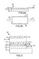
- FIGS. 2 a - 2 ba standard structure of a glass ITO heater 200 is illustrated.
- the heater 200includes a glass plate 204 , an ITO layer 208 disposed over one surface of the plate 204 , and a pair of connectors 212 (e.g., FPC connectors) electrically connected to electrodes of the ITO layer 208 at opposing ends of the ITO layer 208 .
- FPC connectorse.g., FPC connectors
- a device or assembly 300is formed by attaching the heater 200 to the LCD device 10 .
- the ITO layer 208 of the heater 200is interconnected to the second polarizer 58 of the device 10 via a pair of pieces or strips of doubled-sided tape 216 .
- the LC cell 100has been largely represented in FIG. 3 as a schematic box (with only the first and second glass plates 46 , 50 being shown) and the connectors 212 of the glass ITO heater 200 have been removed.
- an air gap 220naturally exists between the ITO layer 208 of the heater 200 and the second polarizer 58 due to the use of the double-sided tape 216 .
- a backlight 224is provided to transmit light through the glass plate 204 of the heater 200 , the second polarizer 58 , etc. so as to produce an appropriate image with the device 10 .
- Any appropriate controller or drivermay pass an applied voltage via the connector 212 to the electrodes of the ITO layer 208 to produce heat that is transmitted towards and through the second polarizer 58 , the second transparent plate 50 , the second ITO layer 22 and the second polyimide layer 38 , and eventually to the LC material 14 to reduce the viscosity thereof.
- the inventorhas determined that utilizing a glass ITO heater to heat LC material in the manner discussed above includes a number of shortcomings that limit the ability of the heater to effectively reduce the viscosity of the LC material and/or limit the performance of the assembly 300 .
- the air gap 220 between the heater 200 and the device 10causes light reflection and corresponding light transmission loss as light transmitted from the backlight 224 passes into the air gap 220 towards the second polarizer 58 .
- the thickness of the air gap 220is often uneven which increases the likelihood of “Mura” defects (i.e., irregular luminosity variation defects) in resulting images.
- light rays traveling from the backlight 224can experience low-levels of birefringence as they travel through the glass plate 204 .
- the above manner of heating the LC material 14is inefficient as the generated heat must travel through a number of layers (e.g., the second polarizer 58 , the second transparent plate 50 , etc.) before eventually reaching the LC material 14 .
- the glass plate 104 of the heater 100is unnecessarily thick and susceptible to breakage, and the resistance of the ITO layer 108 may be affected over time due to oxidation and exposure to air (e.g., via the air gap 120 ).
- the LCD cellincludes first and second transparent plates arranged parallel to each other. Each of the first and second transparent plates includes opposed inner and outer surfaces and the inner surfaces of the first and second transparent plates face each other.
- the LCD cellalso includes first and second transparent conductive layers respectively formed on the inner surfaces of the first and second transparent plates; and a liquid crystal material sealed between the first and second transparent conductive layers.
- the heaterincludes a transparent substrate having opposed first and second surfaces and a third transparent conductive layer formed on the first surface of the substrate.
- the third transparent conductive layeris adapted to generate heat upon flowing a current therethrough, and the heater is disposed against the outer surface of the second transparent plate of the LCD cell so that the device is free of air gaps between the second transparent layer and the third transparent conductive layer.
- the devicemay include a first polarizer including a polarizing axis disposed over the outer surface of the first transparent plate and a second polarizer including a polarizing axis disposed over the second surface of the substrate, where the polarizing axes of the two polarizers are different.
- the devicemay include an optically clear adhesive (OCA) disposed between the second transparent layer and the third transparent conductive layer to secure the third transparent conductive layer to the outer surface of the second transparent plate.
- the transparent substratemay include a film such as a cellulose triacetate (TAC) or a cyclic olefin polymer (COP).
- First and second conductive bus barsmay be formed on opposing sides of the third transparent conductive layer.
- a single connectormay be electrically interconnected to the first and second bus bars and electrically interconnectable to a controller for facilitating generation of heat by the third transparent conductive layer.
- a backlightmay be interconnected to the second polarizer and be adapted to transmit light rays through the second polarizer.
- a heater for a LCDincluding a transparent film, a transparent conductive layer formed on a surface of the transparent film, and first and second spaced bus bars disposed over a surface of the transparent conductive layer, where the transparent conductive layer is adapted to generate heat upon flowing a current therethrough via the first and second bus bars.
- the heatermay include an OCA disposed over the transparent conductive layer and the first and second bus bars.
- a single connectormay be electrically interconnected to the first and second bus bars and electrically interconnectable to a controller for facilitating generation of heat by the transparent conductive layer via the first and second bus bars.
- Each of the first and second bus barsmay include first and second ends respectively extending between first and second ends of the transparent conductive layer, where the single connector is electrically interconnected to the first ends of the first and second bus bars.
- Also disclosed hereinis a method of creating a heater including applying a transparent conductive layer to a surface of a transparent film, and applying at least first and second conductive bus bars to the transparent film surface over the transparent conductive layer, where each of the first and second conductive bus bars extends from a first end of the transparent conductive layer to a second end of the transparent conductive layer.
- the methodalso includes laminating an OCA layer over the transparent conductive layer and the first and second conductive bus bars.
- a single FPC connectormay be bonded to the first and second conductive bus bars adjacent one of the first and second ends of the transparent conductive layer.
- the methodmay also include providing an LC cell that includes front and rear transparent plates arranged parallel to each other, front and rear transparent conductive layers respectively formed on inner surfaces of the front and rear transparent plates, and a liquid crystal material sealed between the front and rear transparent conductive layers; laminating the heater directly to the rear transparent plate of the LC cell using the OCA; laminating a front polarizer having a first axis of light transmission to the front transparent plate of the LC cell; and laminating a rear polarizer having a second axis of light transmission to the transparent film of the heater, where the first axis of transmission is different than the second axis of transmission.
- a backlightmay be secured to the rear polarizer.
- Also disclosed hereinis a method including providing a heater having a transparent film, a transparent conductive layer formed on a surface of the transparent film, first and second spaced bus bars disposed over the transparent film, and an OCA disposed over the transparent conductive layer and the first and second bus bars; providing a LC cell that includes front and rear transparent plates arranged parallel to each other, front and rear transparent conductive layers respectively formed on inner surfaces of the front and rear transparent plates, and a liquid crystal material sealed between the front and rear transparent conductive layers; and laminating the heater directly to the rear transparent plate of the LC cell using the OCA.
- the methodmay include laminating a front polarizer having a first polarizing axis to the front transparent plate of the LC cell, and laminating a rear polarizer having a second polarizing axis to the transparent film of the heater, where the first polarizing axis is perpendicular to the second polarizing axis.
- FIG. 1is a sectional view of an LCD device according to the prior art.
- FIG. 2 ais a side sectional view of a glass ITO heater usable with the LCD device of FIG. 1 , according to the prior art.
- FIG. 2 bis a top view of the glass ITO heater of FIG. 2 a.
- FIG. 3is a side sectional view of an assembly including the LCD device of FIG. 1 and the glass ITO heater of FIG. 2 a.
- FIG. 4is a side sectional view of an LC cell according to one embodiment.
- FIG. 5 ais a side sectional view of a heater according to one embodiment.
- FIG. 5 bis a top view of the heater of FIG. 5 a.
- FIG. 6is an LCD assembly including the LC cell of FIG. 4 and the heater of FIGS. 5 a - 5 b , according to one embodiment.
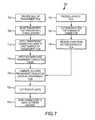
- FIG. 7is a flow diagram illustrating a method that may be used to manufacture the heater of FIGS. 5 a - 5 b.
- FIG. 8is a flow diagram illustrating a method that may be used to manufacture the LCD assembly of FIG. 6 .
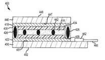
- an LC cell 400includes an LC material 414 (which may be divided into a number of pixels and/or sub-pixels) that is operable to selectively allow light to pass through the LC cell 400 (e.g., from any appropriate backlight) based upon a particular voltage level applied to various pixels or sub-pixels of the LC material 414 .
- the LC cell 400includes first (e.g., front) and second (e.g., rear) transparent conductive (e.g., ITO) layers 418 , 422 .
- Each of the transparent conductive layers 418 , 422includes a plurality of any appropriate arrangement and shape of electrodes (e.g., such as a plurality of rows and columns of strip electrodes, not shown), where electrodes of one of the layers 418 , 422 are common electrodes and the electrodes of the other of the layers 418 , 422 are segment electrodes. While not shown, each of the transparent conductive layers 418 , 422 includes a plurality of conductive output traces electrically interconnected to the respective plurality of electrodes. Conductive spacers 416 may be electrically interconnected between the conductive traces of the transparent conductive layers 418 , 422 and may serve to space apart the transparent conductive layers 418 , 422 .
- a seal frit 430may be used to seal a space between the first and second transparent conductive layers 418 , 422 to contain the LC material 414 . While at least the majority of the seal frit 430 may be allowed to harden in any appropriate manner (e.g., drying, curing), an aperture (not shown) may be formed or left in the seal frit 430 to allow for the introduction of the LC material 414 into the space between the first and second transparent conductive layers 418 , 422 which may be subsequently sealed or otherwise closed.
- any appropriate alignment layerssuch as first and second polyimide layers 434 , 438 having first and second respectively grooved surfaces (not shown) may be respectively disposed on inside surfaces of the first and second transparent conductive layers 418 , 422 so as to align the molecules of the LC material 414 in the direction of the grooved surfaces in the absence of an applied electric field.
- One or more additional spacers 442may be included to space apart the first and second polyimide layers 434 , 438 .
- the LC cell 400also may include parallel first (e.g., front) and second (e.g., rear) transparent plates 446 , 450 (e.g., glass or plastic plates) having respective inner surfaces 447 , 451 and outer surfaces 448 , 452 .
- the first and second transparent conductive layers 418 , 422may be appropriately formed (e.g., via screen printing, etching, etc.) on the inner surfaces 447 , 451 of the first and second transparent plates 446 , 450 .
- the LC cell 400may also include at least one connector 460 (e.g., FPC connector) and at least one driver 462 that may be electrically interconnected to the LC cell 400 at any appropriate location (e.g., as shown, to the second transparent plate 450 ) for applying a voltage to the LC molecules of various pixels or sub-pixels of the LC cell 400 (via the electrodes of the first and second ITO layers 418 , 422 ) so as to position the LC molecules in a particular orientation. More specifically, the driver 462 serves to flow a current through conductive traces of the second ITO layer 422 which current passes through the conductive spacers 426 to the conductive traces of the first ITO layer 418 .
- the driver 462serves to flow a current through conductive traces of the second ITO layer 422 which current passes through the conductive spacers 426 to the conductive traces of the first ITO layer 418 .
- the driver 462may be directly electrically interconnected to the conductive traces of the second ITO layer 422 or else directly electrically interconnected to one or more intermediate conductive traces or wires that are directly electrically interconnected to the conductive traces of the second ITO layer 422 .
- the LC cell 400 of FIG. 4(as well as other components disclosed herein) is not drawn to scale. For example, the size of the spacers 426 , 442 relative to the volume of LC material 414 is greatly exaggerated. Further, in order to apply a voltage across the LC material 414 , a voltage difference must be created between the two transparent conductive layers 418 , 422 .
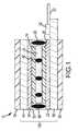
- the heater 500includes a substrate 504 having opposed first and second surfaces 508 , 512 .
- the substrate 504may be a transparent film having high levels of light transmittance and low levels of birefringence.
- the substrate 504may be a film or layer of cellulose triacetate (TAC).
- TACcellulose triacetate
- the substratemay be a film or layer of a cyclic olefin polymer (COP), such as ZeonorFilm®, produced by OPTES, Inc. of Tokyo, Japan.
- COPcyclic olefin polymer
- a transparent conductive layer (e.g., ITO) 516 having first and second opposed sides 518 , 520 and first and second opposed ends 522 , 524may be appropriately formed (e.g., via spattering) on the first surface 508 .
- First and second conductive bus bars 528 , 532 of any appropriate conductive materialmay be respectively formed (e.g., via screen printing) over the transparent conductive layer 516 generally adjacent the first and second sides 518 , 520 and generally between the first and second ends 522 , 524
- a single conductive connector 536e.g., an FPC connector
- disposed adjacent one of the first and second ends 522 , 524 of the transparent conductive layer 516 and electrically interconnected to both of the first and second bus bars 528 , 532may be used to facilitate the electrical interconnection of the transparent conductive layer 516 to any appropriate driver, controller, and/or the like (e.g., the same controller to which the connector 460 is electrically connected).
- the heater 500may in some embodiments utilize only the single connector 536 which advantageously simplifies the design of the heater 500 .
- the connector 536may include a base 540 in addition to first and second legs 544 , 548 (e.g., conductive wires, strips, etc.) electrically interconnected to the base 540 and adapted to be respectively electrically interconnected to the first and second bus bars 528 , 532 in any appropriate manner.
- the base 540may be appropriately electrically interconnected to a driver, controller, and/or the like which serves to apply a voltage to the transparent conductive layer 516 which causes the generation of heat.
- the heater 500may also include any appropriate transparent bonding agent or tape such as an optically clear adhesive (OCA) 552 disposed over the transparent conductive layer 516 and the first and second bus bars 528 , 532 (the OCA 552 being removed from FIG. 5 b in the interest of clarity). More specifically, the OCA 552 may be disposed over substantially an entire length and width of the heater 500 to allow the heater 500 to be appropriately secured (e.g., via lamination of the OCA 552 ) to the LC cell 400 in a manner that is substantially free of air gaps (e.g., such as the air gap 220 in FIG. 3 ).
- OCAoptically clear adhesive
- FIG. 7is a flow diagram illustrating a method 700 of manufacturing the heater 500 of FIGS. 5 a - 5 b . While the method 700 will be discussed in the context of a roll-to-roll system, it is envisioned that other manners of manufacturing the heater 500 may be used.
- a roll of any appropriate transparent filmmay be provided such as a roll of TAC film, a roll of COP film, or the like.
- the rollmay then be mounted onto or otherwise secured to a supply reel of a roll-to-roll system (e.g., a tape or film transport system) made up of a number of rollers for guiding the transparent film through various operational stations, a take-up reel for receiving transparent film that has traveled through the operational stations, and one or more drive motors for inducing movement of the transparent film in first and/or second opposite longitudinal directions.
- a roll-to-roll systeme.g., a tape or film transport system
- a supply reel of a roll-to-roll systemmade up of a number of rollers for guiding the transparent film through various operational stations, a take-up reel for receiving transparent film that has traveled through the operational stations, and one or more drive motors for inducing movement of the transparent film in first and/or second opposite longitudinal directions.
- the roll-to-roll systemmay include or be associated with any appropriate computing system including a processing unit (e.g., CPU), memory unit (e.g., RAM), any appropriate I/O devices (e.g., keyboard, mouse, display, and the like), and one or more programs including protocols or logic storable in the memory unit and executable by the processing unit for controlling operation of the roll-to-roll system.
- a processing unite.g., CPU
- memory unite.g., RAM
- I/O devicese.g., keyboard, mouse, display, and the like
- programsincluding protocols or logic storable in the memory unit and executable by the processing unit for controlling operation of the roll-to-roll system.
- a transparent conductive layere.g., a solid ITO layer such as transparent conductive layer 516 in FIG. 5 a
- a transparent conductive layermay be applied 712 (e.g., via low temperature spattering or the like) at one operational station to a first surface (e.g., first surface 508 ) of the transparent film at one of the operational stations and a plurality of bus bars (e.g., first and second bus bars 528 , 532 ) may be applied (e.g., via printing or the like) at another operational station to the first surface of the transparent film over the transparent conductive layer.
- a transparent conductive layere.g., a solid ITO layer such as transparent conductive layer 516 in FIG. 5 a
- a plurality of bus barse.g., first and second bus bars 528 , 532
- a roll of OCA(e.g., OCA tape) may be provided and mounted to a reel for movement through the roll-to-roll system. Either before or after the OCA is mounted within the system, any appropriate window or opening may be cut or otherwise formed into a portion of the OCA for subsequent bonding of a connector (e.g., FPC) to the bus bars via the window through the OCA.
- a connectore.g., FPC
- FIG. 5 bit can be seen how the first and second legs 544 , 548 of the connector 536 are respectively electrically connected (e.g. via welding, conductive adhesive, or the like) to the first and second bus bars 544 , 548 . While the OCA 552 has been removed for clarity from FIG.
- a linermay be released 728 (e.g., as part of the roll-to-roll process) from one surface (e.g., bottom surface) of the OCA and then the exposed OCA surface may be laminated 732 at another operational station to the transparent film over the transparent conductive layer.
- the filmmay be cut 736 into appropriately sized units (e.g., sized for any appropriate display(s)) and connectors (e.g., FPC connectors such as connector 536 ) may be electrically interconnected to the bus bars to create a heater. See heater 500 of FIGS. 5 a - 5 b.
- FIG. 8is a flow diagram illustrating a method 800 of manufacturing an LCD assembly, such as the LCD assembly 600 of FIG. 6 .
- an LC celle.g., LC cell 400 of FIG. 4
- a heatere.g., heater 500 of FIGS. 5 a - 5 b
- the release linermay be removed 812 to expose the top surface of the OCA.
- the top surface of the OCA of the heatermay be disposed against or at least adjacent the rear transparent plate of LC cell and then the heater may be laminated 816 to the rear transparent plate of the LC cell.
- the OCA 552 of the heater 500is disposed against the second/rear transparent plate 450 of the LC cell 400 .
- the LC cell 400has been largely represented in FIG. 6 as a schematic box (with only the first and second transparent plates 446 , 450 being shown) and the connector 536 of the heater 500 has been removed.
- the method 800may include laminating 820 a front polarizer (e.g., via a thin glue layer disposed on a bottom side of the front polarizer and exposed via removal of a release liner) to the first/front transparent plate of the LC cell and a rear polarizer to the second/bottom surface of the transparent film.
- a front polarizere.g., via a thin glue layer disposed on a bottom side of the front polarizer and exposed via removal of a release liner
- the LCD assembly 600 of FIG. 6illustrates a first (e.g., front) polarizer 654 being appropriately secured to the first transparent plate 446 and a second (e.g., rear) polarizer 658 being appropriately secured to the substrate 504 (e.g., transparent film) of the heater 500 .
- the method 800may also query 824 whether any bubbles or air gaps need to be removed from the OCA and/or any other portions of the LCD assembly. In response to an affirmative answer at 824 , the method 800 may proceed to perform 828 any appropriate autoclave (i.e., high pressure) process to eliminate or at least reduce the likelihood of bubbles, air gaps, and the like within the various portions of the LCD assembly. In any event, the LCD assembly may also be tested 832 and packaged 836 in any appropriate manner. At any appropriate time, a backlight 624 may be appropriately secured to the second polarizer 658 for generating and transmitting light rays through the second polarizer and heater 500 towards the LC cell 400 and the first polarizer 654 .
- any appropriate autoclavei.e., high pressure
- the heater 500 and assembly 600 disclosed hereinpresent a number of advantages over current technologies for heating LC (or other) material of various types of displays.
- a transparent filme.g., TAC, COP, and/or the like
- use of a transparent filmadvantageously avoids or at least reduces birefringence of light rays passing through the substrate and the attendant reduction in image quality associated therewith.
- use of such transparent filmsallows for a great reduction in thickness of the heater 500 (e.g., down to about 0.15 mm) as compared to glass-based ITO heaters.
- use of an OCA to optically bond or laminate the heater 500 to the LC cell 400advantageously eliminates or greatly reduces the occurrence of air gaps, bubbles and the like between and among the second/rear transparent plate 450 of the LC cell 400 and the heater 500 .
- reflection and corresponding transmission loss of light as the light travels from the backlight 624 through the second/rear polarizer 658 and the heater 500 before traveling through the LC cell 400can be reduced.
- positioning of the heater 500 directly against the second/rear transparent plate 450advantageously increases the heating efficiency of the heater 500 because the generated heat need not additionally travel through the second/rear polarizer (i.e., the heater 500 is positioned closer to the LC material 414 of the LC cell 400 ).
- use of the first and second bus bars 528 , 532advantageously allows for use of only a single connector (e.g., connector 536 ) to electrically interconnect the transparent conductive layer 516 of the heater 500 to control electronics which simplifies the overall design of the heater 500 .
Landscapes
- Physics & Mathematics (AREA)
- Nonlinear Science (AREA)
- Mathematical Physics (AREA)
- Chemical & Material Sciences (AREA)
- Crystallography & Structural Chemistry (AREA)
- General Physics & Mathematics (AREA)
- Optics & Photonics (AREA)
- Liquid Crystal (AREA)
Abstract
Description
Claims (20)
Priority Applications (1)
| Application Number | Priority Date | Filing Date | Title |
|---|---|---|---|
| US13/362,310US8525955B2 (en) | 2012-01-31 | 2012-01-31 | Heater for liquid crystal display |
Applications Claiming Priority (1)
| Application Number | Priority Date | Filing Date | Title |
|---|---|---|---|
| US13/362,310US8525955B2 (en) | 2012-01-31 | 2012-01-31 | Heater for liquid crystal display |
Publications (2)
| Publication Number | Publication Date |
|---|---|
| US20130194523A1 US20130194523A1 (en) | 2013-08-01 |
| US8525955B2true US8525955B2 (en) | 2013-09-03 |
Family
ID=48869926
Family Applications (1)
| Application Number | Title | Priority Date | Filing Date |
|---|---|---|---|
| US13/362,310Active2032-03-29US8525955B2 (en) | 2012-01-31 | 2012-01-31 | Heater for liquid crystal display |
Country Status (1)
| Country | Link |
|---|---|
| US (1) | US8525955B2 (en) |
Cited By (4)
| Publication number | Priority date | Publication date | Assignee | Title |
|---|---|---|---|---|
| US10625428B2 (en)* | 2018-06-26 | 2020-04-21 | Amazon Technologies, Inc. | End effector with selectively deformable interface |
| US11247347B2 (en) | 2019-09-20 | 2022-02-15 | Amazon Technologies, Inc. | Linkage system for prehending objects using impactive forces |
| US11267137B1 (en) | 2019-11-25 | 2022-03-08 | Amazon Technologies, Inc. | Controlling end effector suction area using expandable bladder |
| US11642793B1 (en) | 2020-06-12 | 2023-05-09 | Amazon Technologies, Inc. | Varying strength interface system for robotic end-effector |
Families Citing this family (9)
| Publication number | Priority date | Publication date | Assignee | Title |
|---|---|---|---|---|
| US20160249413A1 (en)* | 2015-02-23 | 2016-08-25 | Electronics And Telecommunications Research Institute | Transparent planar heater |
| CN104714325B (en)* | 2015-03-18 | 2017-09-19 | 深圳市华星光电技术有限公司 | Liquid crystal display and preparation method thereof |
| WO2018016647A1 (en)* | 2016-07-21 | 2018-01-25 | シチズンファインデバイス株式会社 | Liquid crystal display apparatus |
| JP2020167047A (en)* | 2019-03-29 | 2020-10-08 | 日東電工株式会社 | heater |
| US10962818B1 (en)* | 2019-09-16 | 2021-03-30 | Rockwell Collins, Inc. | System and method for optimizing warm-up time on large format displays |
| US20220003903A1 (en)* | 2020-07-01 | 2022-01-06 | Shenzhen China Star Optoelectronics Semiconductor Display Technology Co., Ltd. | Quantum dot color filter substrate, manufacturing method thereof, and display panel |
| CN112213878A (en)* | 2020-11-04 | 2021-01-12 | 中航华东光电有限公司 | Device for improving heating efficiency of liquid crystal module |
| CN115390330B (en)* | 2022-09-14 | 2025-05-06 | 光羿智能科技(苏州)有限公司 | Conductive substrate, adjustable light device and rearview mirror |
| GB2637535A (en)* | 2024-01-26 | 2025-07-30 | Envisics Ltd | Thin shutter stack |
Citations (177)
| Publication number | Priority date | Publication date | Assignee | Title |
|---|---|---|---|---|
| US4550221A (en) | 1983-10-07 | 1985-10-29 | Scott Mabusth | Touch sensitive control device |
| US5062198A (en) | 1990-05-08 | 1991-11-05 | Keytec, Inc. | Method of making a transparent touch screen switch assembly |
| US5379057A (en) | 1988-11-14 | 1995-01-03 | Microslate, Inc. | Portable computer with touch screen and computer system employing same |
| US5459463A (en) | 1990-05-25 | 1995-10-17 | Sextant Avionique | Device for locating an object situated close to a detection area and a transparent keyboard using said device |
| US5488204A (en) | 1992-06-08 | 1996-01-30 | Synaptics, Incorporated | Paintbrush stylus for capacitive touch sensor pad |
| US5495077A (en) | 1992-06-08 | 1996-02-27 | Synaptics, Inc. | Object position and proximity detector |
| US5543592A (en) | 1993-07-23 | 1996-08-06 | Sextant Avionique | Multimode manipulator |
| US5543588A (en) | 1992-06-08 | 1996-08-06 | Synaptics, Incorporated | Touch pad driven handheld computing device |
| US5543590A (en) | 1992-06-08 | 1996-08-06 | Synaptics, Incorporated | Object position detector with edge motion feature |
| US5650597A (en) | 1995-01-20 | 1997-07-22 | Dynapro Systems, Inc. | Capacitive touch sensor |
| US5730165A (en) | 1995-12-26 | 1998-03-24 | Philipp; Harald | Time domain capacitive field detector |
| US5825352A (en) | 1996-01-04 | 1998-10-20 | Logitech, Inc. | Multiple fingers contact sensing method for emulating mouse buttons and mouse operations on a touch sensor pad |
| US5854450A (en) | 1995-04-19 | 1998-12-29 | Elo Touchsystems, Inc. | Acoustic condition sensor employing a plurality of mutually non-orthogonal waves |
| US5854625A (en) | 1996-11-06 | 1998-12-29 | Synaptics, Incorporated | Force sensing touchpad |
| US5861583A (en) | 1992-06-08 | 1999-01-19 | Synaptics, Incorporated | Object position detector |
| US5880411A (en) | 1992-06-08 | 1999-03-09 | Synaptics, Incorporated | Object position detector with edge motion feature and gesture recognition |
| US5920310A (en) | 1996-11-15 | 1999-07-06 | Synaptics, Incorporated | Electronic device employing a touch sensitive transducer |
| US5940065A (en) | 1996-03-15 | 1999-08-17 | Elo Touchsystems, Inc. | Algorithmic compensation system and method therefor for a touch sensor panel |
| US5943052A (en) | 1997-08-12 | 1999-08-24 | Synaptics, Incorporated | Method and apparatus for scroll bar control |
| US6091406A (en) | 1996-12-25 | 2000-07-18 | Elo Touchsystems, Inc. | Grating transducer for acoustic touchscreens |
| US6188391B1 (en) | 1998-07-09 | 2001-02-13 | Synaptics, Inc. | Two-layer capacitive touchpad and method of making same |
| US6236391B1 (en) | 1995-01-24 | 2001-05-22 | Elo Touchsystems, Inc. | Acoustic touch position sensor using a low acoustic loss transparent substrate |
| KR200229845Y1 (en) | 2001-02-23 | 2001-07-19 | 주식회사 에이터치 | Structure of Contact of Substrate in Touch Screen |
| US6288707B1 (en) | 1996-07-29 | 2001-09-11 | Harald Philipp | Capacitive position sensor |
| US6297811B1 (en) | 1999-06-02 | 2001-10-02 | Elo Touchsystems, Inc. | Projective capacitive touchscreen |
| US20010026330A1 (en) | 2000-03-28 | 2001-10-04 | Oh Hyeok-Jin | Liquid crystal display employing touch panel |
| US20020030666A1 (en) | 1999-01-25 | 2002-03-14 | Harald Philipp | Capacitive position sensor |
| US6373474B1 (en) | 1998-10-27 | 2002-04-16 | Pentel Kabushiki Kaisha | Real contact type touch panel apparatus |
| US6380929B1 (en) | 1996-09-20 | 2002-04-30 | Synaptics, Incorporated | Pen drawing computer input device |
| US6379509B2 (en) | 1998-01-20 | 2002-04-30 | 3M Innovative Properties Company | Process for forming electrodes |
| US6441809B2 (en) | 1995-01-24 | 2002-08-27 | Elo Touchsystems, Inc. | Acoustic touch position sensor using a low acoustic loss transparent substrate |
| US6452514B1 (en) | 1999-01-26 | 2002-09-17 | Harald Philipp | Capacitive sensor and array |
| US20020145593A1 (en) | 2001-04-06 | 2002-10-10 | 3M Innovative Properties Company | Frontlit illuminated touch panel |
| US6466036B1 (en) | 1998-11-25 | 2002-10-15 | Harald Philipp | Charge transfer capacitance measurement circuit |
| US6488981B1 (en) | 2001-06-20 | 2002-12-03 | 3M Innovative Properties Company | Method of manufacturing a touch screen panel |
| US6492979B1 (en) | 1999-09-07 | 2002-12-10 | Elo Touchsystems, Inc. | Dual sensor touchscreen utilizing projective-capacitive and force touch sensors |
| US20020191029A1 (en) | 2001-05-16 | 2002-12-19 | Synaptics, Inc. | Touch screen with user interface enhancement |
| US6504583B2 (en) | 1998-10-02 | 2003-01-07 | 3M Innovative Properties Company | Anti-microbial touch panel and method of making same using homeotropic liquid crystal silanes |
| US6504530B1 (en) | 1999-09-07 | 2003-01-07 | Elo Touchsystems, Inc. | Touch confirming touchscreen utilizing plural touch sensors |
| US6549193B1 (en) | 1998-10-09 | 2003-04-15 | 3M Innovative Properties Company | Touch panel with improved linear response and minimal border width electrode pattern |
| US6555235B1 (en) | 2000-07-06 | 2003-04-29 | 3M Innovative Properties Co. | Touch screen system |
| US20030095111A1 (en) | 2001-11-14 | 2003-05-22 | In-Duk Song | Touch panel |
| US20030103043A1 (en) | 2001-11-30 | 2003-06-05 | 3M Innovative Properties Company | System and method for locating a touch on a capacitive touch screen |
| US6587097B1 (en) | 2000-11-28 | 2003-07-01 | 3M Innovative Properties Co. | Display system |
| US20030132922A1 (en) | 2002-01-17 | 2003-07-17 | Harald Philipp | Touch screen detection apparatus |
| US20030184523A1 (en) | 2002-03-29 | 2003-10-02 | 3M Innovative Properties Company | Moisture deflector for capacitive NFI touch screens for use with bezels of conductive material |
| US20030205450A1 (en) | 2002-05-02 | 2003-11-06 | 3M Innovative Properties Company | Pressure activated switch and touch panel |
| US20040008129A1 (en) | 2002-07-12 | 2004-01-15 | Harald Philipp | Keyboard with reduced keying ambiguity |
| US20040061687A1 (en) | 2002-09-17 | 2004-04-01 | Elo Touchsystems, Inc. | Dynamic corrections for a non-linear touchscreen |
| US20040100448A1 (en) | 2002-11-25 | 2004-05-27 | 3M Innovative Properties Company | Touch display |
| US20040104826A1 (en) | 2002-10-31 | 2004-06-03 | Harald Philipp | Charge transfer capacitive position sensor |
| US20040135773A1 (en) | 2002-12-24 | 2004-07-15 | Bang Yong Ik | Touch panel integrated with liquid crystal display |
| US6784873B1 (en) | 2000-08-04 | 2004-08-31 | Peter V. Boesen | Method and medium for computer readable keyboard display incapable of user termination |
| US20040188150A1 (en) | 2003-03-25 | 2004-09-30 | 3M Innovative Properties Company | High transparency touch screen |
| US20040189882A1 (en) | 1999-04-13 | 2004-09-30 | Jeong Yun Cheol | Polarizer integrated with transparent conductive film, a touch panel integrated with the polarizer and a flat panel display integrated with the touch panel |
| JP2004280720A (en) | 2003-03-18 | 2004-10-07 | Kawaguchiko Seimitsu Co Ltd | Touch panel and screen input type display device provided with it |
| US6819316B2 (en) | 2001-04-17 | 2004-11-16 | 3M Innovative Properties Company | Flexible capacitive touch sensor |
| US20040252109A1 (en) | 2002-04-11 | 2004-12-16 | Synaptics, Inc. | Closed-loop sensor on a solid-state object position detector |
| US20050024341A1 (en) | 2001-05-16 | 2005-02-03 | Synaptics, Inc. | Touch screen with user interface enhancement |
| US6856259B1 (en) | 2004-02-06 | 2005-02-15 | Elo Touchsystems, Inc. | Touch sensor system to detect multiple touch events |
| US20050035953A1 (en) | 2003-06-20 | 2005-02-17 | Richard Woolley | Single-layer touchpad and methods of use |
| US20050041018A1 (en) | 2003-08-21 | 2005-02-24 | Harald Philipp | Anisotropic touch screen element |
| US20050052429A1 (en) | 2003-08-21 | 2005-03-10 | Harald Philipp | Capacitive position sensor |
| US20050078027A1 (en) | 2003-10-08 | 2005-04-14 | Harald Philipp | Touch sensitive control panel |
| US20050110766A1 (en) | 2003-11-24 | 2005-05-26 | Elo Touchsystems, Inc. | Touch sensor with conductive polymer switches |
| US20050110767A1 (en) | 2003-11-24 | 2005-05-26 | Elo Touchsystems, Inc. | Method of manufacturing touch sensor with switch tape strips |
| US6904570B2 (en) | 2001-06-07 | 2005-06-07 | Synaptics, Inc. | Method and apparatus for controlling a display of data on a display screen |
| US20050162408A1 (en) | 2004-01-27 | 2005-07-28 | Elo Touchsystems, Inc. | Capacitive touch sensor |
| US20050174335A1 (en) | 2004-02-10 | 2005-08-11 | Elo Touchsystems, Inc. | Resistive touchscreen with programmable display coversheet |
| US20050179673A1 (en) | 2004-02-13 | 2005-08-18 | Harald Philipp | Capacitive sensor |
| US6943705B1 (en) | 2002-05-03 | 2005-09-13 | Synaptics, Inc. | Method and apparatus for providing an integrated membrane switch and capacitive sensor |
| US6961049B2 (en) | 2002-06-21 | 2005-11-01 | 3M Innovative Properties Company | Capacitive touch sensor architecture with unique sensor bar addressing |
| US20050246459A1 (en) | 2003-07-11 | 2005-11-03 | Harald Philipp | Keyboard With Reduced Keying Ambiguity |
| US20050260338A1 (en) | 2004-05-19 | 2005-11-24 | Trendon Touch Technology Corp. | Method of manufacturing circuit layout on touch panel by utilizing metal plating technology |
| US6970160B2 (en) | 2002-12-19 | 2005-11-29 | 3M Innovative Properties Company | Lattice touch-sensing system |
| US6977646B1 (en) | 2001-11-30 | 2005-12-20 | 3M Innovative Properties Co. | Touch screen calibration system and method |
| US7000474B2 (en) | 2003-02-28 | 2006-02-21 | Elo Touchsystems, Inc. | Acoustic device using higher order harmonic piezoelectric element |
| US7006081B2 (en) | 2000-10-20 | 2006-02-28 | Elo Touchsystems, Inc. | Acoustic touch sensor with laminated substrate |
| US7030860B1 (en) | 1999-10-08 | 2006-04-18 | Synaptics Incorporated | Flexible transparent touch sensing system for electronic devices |
| US20060097991A1 (en) | 2004-05-06 | 2006-05-11 | Apple Computer, Inc. | Multipoint touchscreen |
| US20060132462A1 (en) | 2004-12-22 | 2006-06-22 | 3M Innovative Properties Company | Touch sensors incorporating capacitively coupled electrodes |
| US20060139340A1 (en) | 2001-10-03 | 2006-06-29 | 3M Innovative Properties Company | Touch panel system and method for distinguishing multiple touch inputs |
| US20060187214A1 (en) | 1992-06-08 | 2006-08-24 | Synaptics, Inc, A California Corporation | Object position detector with edge motion feature and gesture recognition |
| US20060192690A1 (en) | 2002-07-12 | 2006-08-31 | Harald Philipp | Capacitive Keyboard with Non-Locking Reduced Keying Ambiguity |
| US7102621B2 (en) | 1997-09-30 | 2006-09-05 | 3M Innovative Properties Company | Force measurement system correcting for inertial interference |
| US20060202970A1 (en) | 2005-03-11 | 2006-09-14 | Jia-Yih Lii | Touchpad with single-layered printed circuit board structure |
| US7109976B2 (en) | 2003-04-01 | 2006-09-19 | 3M Innovative Properties Company | Display screen seal |
| CN1838151A (en) | 2005-03-22 | 2006-09-27 | 义隆电子股份有限公司 | Single-layer printed circuit board structure touch panel |
| US20060238513A1 (en) | 2004-05-21 | 2006-10-26 | Harald Philipp | Touch sensitive control panel |
| US7129935B2 (en) | 2003-06-02 | 2006-10-31 | Synaptics Incorporated | Sensor patterns for a capacitive sensing apparatus |
| US20060274047A1 (en) | 2005-06-02 | 2006-12-07 | Eastman Kodak Company | Touchscreen with one carbon nanotube conductive layer |
| US20060274055A1 (en) | 2005-06-01 | 2006-12-07 | Synaptics Incorporated | Touch pad with flexible substrate |
| US7148882B2 (en) | 2003-05-16 | 2006-12-12 | 3M Innovatie Properties Company | Capacitor based force sensor |
| US7151532B2 (en) | 2002-08-09 | 2006-12-19 | 3M Innovative Properties Company | Multifunctional multilayer optical film |
| US20060284836A1 (en) | 2005-06-17 | 2006-12-21 | Harald Philipp | Control Panel |
| US7154481B2 (en) | 2002-06-25 | 2006-12-26 | 3M Innovative Properties Company | Touch sensor |
| US7158122B2 (en) | 2002-05-17 | 2007-01-02 | 3M Innovative Properties Company | Calibration of force based touch panel systems |
| US20070002192A1 (en) | 2005-06-29 | 2007-01-04 | Casio Computer Co., Ltd. | Liquid crystal display apparatus including touch panel |
| US20070008299A1 (en) | 2005-07-08 | 2007-01-11 | Harald Philipp | Two-Dimensional Position Sensor |
| US20070026089A1 (en) | 2005-07-29 | 2007-02-01 | Trendon Touch Technology Corp. | Touch screen with bacteria inhibition layer and manufacturing method thereof |
| US7176902B2 (en) | 2003-10-10 | 2007-02-13 | 3M Innovative Properties Company | Wake-on-touch for vibration sensing touch input devices |
| US7176897B2 (en) | 2002-05-17 | 2007-02-13 | 3M Innovative Properties Company | Correction of memory effect errors in force-based touch panel systems |
| US7183948B2 (en) | 2001-04-13 | 2007-02-27 | 3M Innovative Properties Company | Tangential force control in a touch location device |
| US7190352B2 (en) | 2002-10-31 | 2007-03-13 | Ownway Biotronics Inc. | Method and apparatus of electrotactile panel with pointing system |
| US7190350B2 (en) | 2001-04-13 | 2007-03-13 | 3M Innovative Properties Company | Touch screen with rotationally isolated force sensor |
| US20070062739A1 (en) | 2005-09-20 | 2007-03-22 | Harald Philipp | Touch Sensitive Screen |
| US20070074914A1 (en) | 2005-10-05 | 2007-04-05 | Geaghan Bernard O | Interleaved electrodes for touch sensing |
| US7202859B1 (en) | 2002-08-09 | 2007-04-10 | Synaptics, Inc. | Capacitive sensing pattern |
| US20070085838A1 (en) | 2005-10-17 | 2007-04-19 | Ricks Theodore K | Method for making a display with integrated touchscreen |
| US7212189B2 (en) | 1999-11-04 | 2007-05-01 | Synaptics Incorporated | Capacitive mouse |
| US20070103446A1 (en) | 2005-11-04 | 2007-05-10 | Trendon Touch Technology Corp. | Wiring of touch panel |
| US20070109274A1 (en) | 2005-11-15 | 2007-05-17 | Synaptics Incorporated | Methods and systems for detecting a position-based attribute of an object using digital codes |
| US7227538B2 (en) | 2004-02-25 | 2007-06-05 | 3M Innovative Properties Company | Touch sensor with linearized response |
| US7236161B2 (en) | 2003-03-21 | 2007-06-26 | 3M Innovative Properties Company | Remote touch simulation systems and methods |
| US20070159561A1 (en) | 2006-01-10 | 2007-07-12 | Trendon Touch Technology Corp. | Display panel having touching circuit |
| US20070176906A1 (en) | 2006-02-01 | 2007-08-02 | Synaptics Incorporated | Proximity sensor and method for indicating extended interface results |
| US7253643B1 (en) | 2006-07-19 | 2007-08-07 | Cypress Semiconductor Corporation | Uninterrupted radial capacitive sense interface |
| US20070222766A1 (en) | 2006-03-24 | 2007-09-27 | Synaptics Incorporated | Touch sensor effective area enhancement |
| US7277087B2 (en) | 2003-12-31 | 2007-10-02 | 3M Innovative Properties Company | Touch sensing with touch down and lift off sensitivity |
| US20070229466A1 (en) | 2006-03-30 | 2007-10-04 | Cypress Semiconductor Corporation | Apparatus and method for recognizing a tap gesture on a touch sensing device |
| US20070229470A1 (en) | 2006-03-31 | 2007-10-04 | Warren Snyder | Capacitive touch sense device having polygonal shaped sensor elements |
| US20070229468A1 (en) | 2006-03-30 | 2007-10-04 | Cypress Semiconductor Corporation | Apparatus and method for reducing average scan rate to detect a conductive object on a sensing device |
| US20070236475A1 (en) | 2006-04-05 | 2007-10-11 | Synaptics Incorporated | Graphical scroll wheel |
| US20070236618A1 (en) | 2006-03-31 | 2007-10-11 | 3M Innovative Properties Company | Touch Screen Having Reduced Visibility Transparent Conductor Pattern |
| US20070247443A1 (en) | 2006-04-25 | 2007-10-25 | Harald Philipp | Hybrid Capacitive Touch Screen Element |
| US20070257894A1 (en) | 2006-05-05 | 2007-11-08 | Harald Philipp | Touch Screen Element |
| US20070257893A1 (en) | 2006-05-02 | 2007-11-08 | Harald Philipp | Touch Screen |
| US20070262962A1 (en) | 2006-05-10 | 2007-11-15 | Cypress Semiconductor Corporation | Apparatus and method for reducing charge time and power consumption of a sensing device |
| US20070264844A1 (en) | 2006-05-10 | 2007-11-15 | Trendon Touch Technology Corp. | Method of hiding transparent electrodes on a transparent substrate |
| US20070262963A1 (en) | 2006-05-11 | 2007-11-15 | Cypress Semiconductor Corporation | Apparatus and method for recognizing a button operation on a sensing device |
| US7298367B2 (en) | 2003-11-25 | 2007-11-20 | 3M Innovative Properties Company | Light emitting stylus and user input device using same |
| US20070268265A1 (en) | 2006-05-18 | 2007-11-22 | Cypress Semiconductor Corporation | Two-pin buttons |
| US20070268266A1 (en) | 2006-05-18 | 2007-11-22 | Cypress Semiconductor Corporation | Toothed slider |
| US20070268276A1 (en) | 2003-06-24 | 2007-11-22 | Kent Joel C | Acoustic Touch Sensor with Low Profile Diffractive Grating Transducer Assembly |
| US20070273561A1 (en) | 2006-05-25 | 2007-11-29 | Harald Philipp | Capacitive Keyboard with Position Dependent Reduced Keying Ambiguity |
| US20070273560A1 (en) | 2006-05-25 | 2007-11-29 | Cypress Semiconductor Corporation | Low pin count solution using capacitance sensing matrix for keyboard architecture |
| US20070279395A1 (en) | 2006-05-31 | 2007-12-06 | Harald Philipp | Two Dimensional Position Sensor |
| US7307624B2 (en) | 2003-12-30 | 2007-12-11 | 3M Innovative Properties Company | Touch sensor with linearized response |
| US20070291009A1 (en) | 2006-06-19 | 2007-12-20 | Cypress Semiconductor Corporation | Apparatus and method for detecting a touch-sensor pad gesture |
| US20070291016A1 (en) | 2006-06-20 | 2007-12-20 | Harald Philipp | Capacitive Position Sensor |
| US20070296709A1 (en) | 2006-06-27 | 2007-12-27 | Cypress Semiconductor Corporation | Apparatus and method for detecting multiple buttons with one pin |
| US7315300B2 (en) | 2003-12-31 | 2008-01-01 | 3M Innovative Properties Company | Touch sensitive device employing impulse reconstruction |
| US20080001925A1 (en) | 2006-06-30 | 2008-01-03 | Cypress Semiconductor Corporation | Navigation panel |
| US20080007534A1 (en) | 2006-07-10 | 2008-01-10 | Cypress Semiconductor Corporation | Touch-sensor with shared capacitive sensors |
| US20080007434A1 (en) | 2006-07-10 | 2008-01-10 | Luben Hristov | Priority and Combination Suppression Techniques (PST/CST) for a Capacitive Keyboard |
| US20080012832A1 (en) | 2006-07-13 | 2008-01-17 | Guanghai Li | Multi-function touchpad |
| US20080024461A1 (en) | 2003-12-15 | 2008-01-31 | 3M Innovative Properties Company | Wiring harness and touch sensor incorporating same |
| US7327352B2 (en) | 2002-06-14 | 2008-02-05 | 3M Innovative Properties Company | Linearized conductive surface |
| US20080029292A1 (en) | 2004-04-20 | 2008-02-07 | Ryuji Takayama | Transparent Conductive Formed Article for a Touch Panel and Touch Panel |
| CN101122839A (en) | 2007-10-11 | 2008-02-13 | 友达光电股份有限公司 | Capacitive touch pad with low impedance structure and manufacturing method thereof |
| US20080048997A1 (en) | 1992-06-08 | 2008-02-28 | Synaptics Incorporated | Object position detector with edge motion feature and gesture recognition |
| US20080062139A1 (en) | 2006-06-09 | 2008-03-13 | Apple Inc. | Touch screen liquid crystal display |
| US20080074398A1 (en) | 2006-09-26 | 2008-03-27 | David Gordon Wright | Single-layer capacitive sensing device |
| US20080111714A1 (en) | 2006-11-14 | 2008-05-15 | Viktor Kremin | Capacitance to code converter with sigma-delta modulator |
| US20080122802A1 (en) | 2006-11-29 | 2008-05-29 | Tsutomu Furuhashi | Liquid crystal dispaly device with touch screen |
| US20080138589A1 (en) | 2005-05-26 | 2008-06-12 | Gunze Limited | Transparent Planar Body and Transparent Touch Switch |
| US20080142352A1 (en) | 2006-12-18 | 2008-06-19 | Wright David G | Two circuit board touch-sensor device |
| US20080143683A1 (en) | 2006-12-15 | 2008-06-19 | Apple Inc. | Pet-based touch pad |
| US20080150905A1 (en) | 2006-12-21 | 2008-06-26 | Grivna Edward L | Feedback mechanism for user detection of reference location on a sensing device |
| US20080150906A1 (en) | 2006-12-22 | 2008-06-26 | Grivna Edward L | Multi-axial touch-sensor device with multi-touch resolution |
| US20080158183A1 (en) | 2007-01-03 | 2008-07-03 | Apple Computer, Inc. | Double-sided touch-sensitive panel with shield and drive combined layer |
| US20080158181A1 (en) | 2007-01-03 | 2008-07-03 | Apple Computer, Inc. | Double-sided touch sensitive panel and flex circuit bonding |
| US20080165158A1 (en) | 2007-01-05 | 2008-07-10 | Apple Inc. | Touch screen stack-ups |
| US20080165139A1 (en) | 2007-01-05 | 2008-07-10 | Apple Inc. | Touch screen stack-up processing |
| US20080264699A1 (en) | 2007-04-27 | 2008-10-30 | Trendon Touch Technology Corp. | Conductor pattern structure of capacitive touch panel |
| US20080309635A1 (en) | 2007-06-14 | 2008-12-18 | Epson Imaging Devices Corporation | Capacitive input device |
| US20090085891A1 (en) | 2007-09-29 | 2009-04-02 | Au Optronics Corporation | Capacitive Touch Panel with Low Impedance |
| US20090160824A1 (en) | 2007-12-25 | 2009-06-25 | Cando Corporation | Sensory structure of touch panel |
| US20090167710A1 (en) | 2007-12-27 | 2009-07-02 | Tsinghua University | Touch panel and display device using the same |
| KR100907512B1 (en) | 2006-12-29 | 2009-07-14 | (주)탑나노시스 | Method of forming a touch panel and a conductive layer of the touch panel |
| US20090194344A1 (en) | 2008-01-31 | 2009-08-06 | Avago Technologies Ecbu Ip (Singapore) Pte. Ltd. | Single Layer Mutual Capacitance Sensing Systems, Device, Components and Methods |
| US20090236151A1 (en) | 2008-03-21 | 2009-09-24 | I-Hau Yeh | Touch Panel Device |
| US20090309850A1 (en) | 2008-06-16 | 2009-12-17 | Kai-Ti Yang | Capacitive touch panel |
| US20100045625A1 (en) | 2008-08-21 | 2010-02-25 | Tpo Displays Corp. | Touch panel and system for displaying images utilizing the same |
| US20100066700A1 (en) | 2008-09-12 | 2010-03-18 | Ocular Lcd Inc. | Capacitive Touch Screen |
| US20100073319A1 (en) | 2008-09-25 | 2010-03-25 | Apple Inc. | Capacitive sensor having electrodes arranged on the substrate and the flex circuit |
| US7945297B2 (en) | 2005-09-30 | 2011-05-17 | Atmel Corporation | Headsets and headset power management |
- 2012
- 2012-01-31USUS13/362,310patent/US8525955B2/enactiveActive
Patent Citations (228)
| Publication number | Priority date | Publication date | Assignee | Title |
|---|---|---|---|---|
| US4550221A (en) | 1983-10-07 | 1985-10-29 | Scott Mabusth | Touch sensitive control device |
| US5675362A (en) | 1988-11-14 | 1997-10-07 | Microslate, Inc. | Portable computer with touch screen and computing system employing same |
| US5379057A (en) | 1988-11-14 | 1995-01-03 | Microslate, Inc. | Portable computer with touch screen and computer system employing same |
| US5062198A (en) | 1990-05-08 | 1991-11-05 | Keytec, Inc. | Method of making a transparent touch screen switch assembly |
| US5459463A (en) | 1990-05-25 | 1995-10-17 | Sextant Avionique | Device for locating an object situated close to a detection area and a transparent keyboard using said device |
| US5495077A (en) | 1992-06-08 | 1996-02-27 | Synaptics, Inc. | Object position and proximity detector |
| US6750852B2 (en) | 1992-06-08 | 2004-06-15 | Synaptics, Inc. | Object position detector with edge motion feature and gesture recognition |
| US5543588A (en) | 1992-06-08 | 1996-08-06 | Synaptics, Incorporated | Touch pad driven handheld computing device |
| US5543590A (en) | 1992-06-08 | 1996-08-06 | Synaptics, Incorporated | Object position detector with edge motion feature |
| US6414671B1 (en) | 1992-06-08 | 2002-07-02 | Synaptics Incorporated | Object position detector with edge motion feature and gesture recognition |
| US6380931B1 (en) | 1992-06-08 | 2002-04-30 | Synaptics Incorporated | Object position detector with edge motion feature and gesture recognition |
| US20040178997A1 (en) | 1992-06-08 | 2004-09-16 | Synaptics, Inc., A California Corporation | Object position detector with edge motion feature and gesture recognition |
| US20080042994A1 (en) | 1992-06-08 | 2008-02-21 | Synaptics Incorporated | Object position detector with edge motion feature and gesture recognition |
| US5841078A (en) | 1992-06-08 | 1998-11-24 | Synaptics, Inc. | Object position detector |
| US20060092142A1 (en) | 1992-06-08 | 2006-05-04 | Synaptics, Inc., A California Corporation | Object position detector with edge motion feature and gesture recognition |
| US20080048997A1 (en) | 1992-06-08 | 2008-02-28 | Synaptics Incorporated | Object position detector with edge motion feature and gesture recognition |
| US5861583A (en) | 1992-06-08 | 1999-01-19 | Synaptics, Incorporated | Object position detector |
| US5880411A (en) | 1992-06-08 | 1999-03-09 | Synaptics, Incorporated | Object position detector with edge motion feature and gesture recognition |
| US5488204A (en) | 1992-06-08 | 1996-01-30 | Synaptics, Incorporated | Paintbrush stylus for capacitive touch sensor pad |
| US7109978B2 (en) | 1992-06-08 | 2006-09-19 | Synaptics, Inc. | Object position detector with edge motion feature and gesture recognition |
| US20060187214A1 (en) | 1992-06-08 | 2006-08-24 | Synaptics, Inc, A California Corporation | Object position detector with edge motion feature and gesture recognition |
| US5543592A (en) | 1993-07-23 | 1996-08-06 | Sextant Avionique | Multimode manipulator |
| US5650597A (en) | 1995-01-20 | 1997-07-22 | Dynapro Systems, Inc. | Capacitive touch sensor |
| US6441809B2 (en) | 1995-01-24 | 2002-08-27 | Elo Touchsystems, Inc. | Acoustic touch position sensor using a low acoustic loss transparent substrate |
| US6236391B1 (en) | 1995-01-24 | 2001-05-22 | Elo Touchsystems, Inc. | Acoustic touch position sensor using a low acoustic loss transparent substrate |
| US7061475B2 (en) | 1995-04-19 | 2006-06-13 | Elo Touchsystems, Inc. | Acoustic condition sensor employing a plurality of mutually non-orthogonal waves |
| US5854450A (en) | 1995-04-19 | 1998-12-29 | Elo Touchsystems, Inc. | Acoustic condition sensor employing a plurality of mutually non-orthogonal waves |
| US6723929B2 (en) | 1995-04-19 | 2004-04-20 | Elo Touchsystems, Inc. | Acoustic condition sensor employing a plurality of mutually non-orthogonal waves |
| US5730165A (en) | 1995-12-26 | 1998-03-24 | Philipp; Harald | Time domain capacitive field detector |
| US5825352A (en) | 1996-01-04 | 1998-10-20 | Logitech, Inc. | Multiple fingers contact sensing method for emulating mouse buttons and mouse operations on a touch sensor pad |
| US5940065A (en) | 1996-03-15 | 1999-08-17 | Elo Touchsystems, Inc. | Algorithmic compensation system and method therefor for a touch sensor panel |
| US6506983B1 (en) | 1996-03-15 | 2003-01-14 | Elo Touchsystems, Inc. | Algorithmic compensation system and method therefor for a touch sensor panel |
| US6288707B1 (en) | 1996-07-29 | 2001-09-11 | Harald Philipp | Capacitive position sensor |
| US6380929B1 (en) | 1996-09-20 | 2002-04-30 | Synaptics, Incorporated | Pen drawing computer input device |
| US5854625A (en) | 1996-11-06 | 1998-12-29 | Synaptics, Incorporated | Force sensing touchpad |
| US5920310A (en) | 1996-11-15 | 1999-07-06 | Synaptics, Incorporated | Electronic device employing a touch sensitive transducer |
| US6091406A (en) | 1996-12-25 | 2000-07-18 | Elo Touchsystems, Inc. | Grating transducer for acoustic touchscreens |
| US5943052A (en) | 1997-08-12 | 1999-08-24 | Synaptics, Incorporated | Method and apparatus for scroll bar control |
| US7102621B2 (en) | 1997-09-30 | 2006-09-05 | 3M Innovative Properties Company | Force measurement system correcting for inertial interference |
| US6379509B2 (en) | 1998-01-20 | 2002-04-30 | 3M Innovative Properties Company | Process for forming electrodes |
| US7303809B2 (en) | 1998-01-20 | 2007-12-04 | 3M Innovative Properties Company | Process for forming electrodes |
| US6188391B1 (en) | 1998-07-09 | 2001-02-13 | Synaptics, Inc. | Two-layer capacitive touchpad and method of making same |
| US6504583B2 (en) | 1998-10-02 | 2003-01-07 | 3M Innovative Properties Company | Anti-microbial touch panel and method of making same using homeotropic liquid crystal silanes |
| US6549193B1 (en) | 1998-10-09 | 2003-04-15 | 3M Innovative Properties Company | Touch panel with improved linear response and minimal border width electrode pattern |
| US6781579B2 (en) | 1998-10-09 | 2004-08-24 | 3M Innovative Properties Company | Touch panel with improved linear response and minimal border width electrode pattern |
| US20030137498A1 (en) | 1998-10-09 | 2003-07-24 | 3M Innovative Properties Company | Touch panel with improved linear response and minimal border width electrode pattern |
| US6373474B1 (en) | 1998-10-27 | 2002-04-16 | Pentel Kabushiki Kaisha | Real contact type touch panel apparatus |
| US6466036B1 (en) | 1998-11-25 | 2002-10-15 | Harald Philipp | Charge transfer capacitance measurement circuit |
| US20020030666A1 (en) | 1999-01-25 | 2002-03-14 | Harald Philipp | Capacitive position sensor |
| US6535200B2 (en) | 1999-01-25 | 2003-03-18 | Harald Philipp | Capacitive position sensor |
| US6452514B1 (en) | 1999-01-26 | 2002-09-17 | Harald Philipp | Capacitive sensor and array |
| US20040189882A1 (en) | 1999-04-13 | 2004-09-30 | Jeong Yun Cheol | Polarizer integrated with transparent conductive film, a touch panel integrated with the polarizer and a flat panel display integrated with the touch panel |
| US6297811B1 (en) | 1999-06-02 | 2001-10-02 | Elo Touchsystems, Inc. | Projective capacitive touchscreen |
| US6504530B1 (en) | 1999-09-07 | 2003-01-07 | Elo Touchsystems, Inc. | Touch confirming touchscreen utilizing plural touch sensors |
| US6492979B1 (en) | 1999-09-07 | 2002-12-10 | Elo Touchsystems, Inc. | Dual sensor touchscreen utilizing projective-capacitive and force touch sensors |
| US7030860B1 (en) | 1999-10-08 | 2006-04-18 | Synaptics Incorporated | Flexible transparent touch sensing system for electronic devices |
| US7212189B2 (en) | 1999-11-04 | 2007-05-01 | Synaptics Incorporated | Capacitive mouse |
| US20010026330A1 (en) | 2000-03-28 | 2001-10-04 | Oh Hyeok-Jin | Liquid crystal display employing touch panel |
| US6555235B1 (en) | 2000-07-06 | 2003-04-29 | 3M Innovative Properties Co. | Touch screen system |
| US6784873B1 (en) | 2000-08-04 | 2004-08-31 | Peter V. Boesen | Method and medium for computer readable keyboard display incapable of user termination |
| US7006081B2 (en) | 2000-10-20 | 2006-02-28 | Elo Touchsystems, Inc. | Acoustic touch sensor with laminated substrate |
| US6587097B1 (en) | 2000-11-28 | 2003-07-01 | 3M Innovative Properties Co. | Display system |
| KR200229845Y1 (en) | 2001-02-23 | 2001-07-19 | 주식회사 에이터치 | Structure of Contact of Substrate in Touch Screen |
| US6738051B2 (en) | 2001-04-06 | 2004-05-18 | 3M Innovative Properties Company | Frontlit illuminated touch panel |
| US20020145593A1 (en) | 2001-04-06 | 2002-10-10 | 3M Innovative Properties Company | Frontlit illuminated touch panel |
| US7253809B2 (en) | 2001-04-06 | 2007-08-07 | 3M Innovative Properties Company | Frontlit illuminated touch panel |
| US20060132453A1 (en) | 2001-04-06 | 2006-06-22 | 3M Innovative Properties Company | Frontlit illuminated touch panel |
| US7196694B2 (en) | 2001-04-13 | 2007-03-27 | 3M Innovative Properties Company | Force sensors and touch panels using same |
| US7190350B2 (en) | 2001-04-13 | 2007-03-13 | 3M Innovative Properties Company | Touch screen with rotationally isolated force sensor |
| US7183948B2 (en) | 2001-04-13 | 2007-02-27 | 3M Innovative Properties Company | Tangential force control in a touch location device |
| US6819316B2 (en) | 2001-04-17 | 2004-11-16 | 3M Innovative Properties Company | Flexible capacitive touch sensor |
| US20050024341A1 (en) | 2001-05-16 | 2005-02-03 | Synaptics, Inc. | Touch screen with user interface enhancement |
| US20020191029A1 (en) | 2001-05-16 | 2002-12-19 | Synaptics, Inc. | Touch screen with user interface enhancement |
| US6904570B2 (en) | 2001-06-07 | 2005-06-07 | Synaptics, Inc. | Method and apparatus for controlling a display of data on a display screen |
| US6842171B2 (en) | 2001-06-20 | 2005-01-11 | 3M Innovative Properties Company | Touch panel having edge electrodes extending through a protective coating |
| US6488981B1 (en) | 2001-06-20 | 2002-12-03 | 3M Innovative Properties Company | Method of manufacturing a touch screen panel |
| US20030001826A1 (en) | 2001-06-20 | 2003-01-02 | 3M Innovative Properties Company | Method of manufacturing a touch screen panel |
| US20070236478A1 (en) | 2001-10-03 | 2007-10-11 | 3M Innovative Properties Company | Touch panel system and method for distinguishing multiple touch inputs |
| US20060139340A1 (en) | 2001-10-03 | 2006-06-29 | 3M Innovative Properties Company | Touch panel system and method for distinguishing multiple touch inputs |
| US7254775B2 (en) | 2001-10-03 | 2007-08-07 | 3M Innovative Properties Company | Touch panel system and method for distinguishing multiple touch inputs |
| US20030095111A1 (en) | 2001-11-14 | 2003-05-22 | In-Duk Song | Touch panel |
| US20030103043A1 (en) | 2001-11-30 | 2003-06-05 | 3M Innovative Properties Company | System and method for locating a touch on a capacitive touch screen |
| US6977646B1 (en) | 2001-11-30 | 2005-12-20 | 3M Innovative Properties Co. | Touch screen calibration system and method |
| US6825833B2 (en) | 2001-11-30 | 2004-11-30 | 3M Innovative Properties Company | System and method for locating a touch on a capacitive touch screen |
| US20060202969A1 (en) | 2001-11-30 | 2006-09-14 | 3M Innovative Properties Company | Method for simulating a touch on a touch screen |
| US20030132922A1 (en) | 2002-01-17 | 2003-07-17 | Harald Philipp | Touch screen detection apparatus |
| US20030184523A1 (en) | 2002-03-29 | 2003-10-02 | 3M Innovative Properties Company | Moisture deflector for capacitive NFI touch screens for use with bezels of conductive material |
| US6927761B2 (en) | 2002-03-29 | 2005-08-09 | 3M Innovative Properties Company | Moisture deflector for capacitive NFI touch screens for use with bezels of conductive material |
| US20080048978A1 (en) | 2002-04-11 | 2008-02-28 | Synaptics Incorporated | Closed-loop sensor on a solid-state object position detector |
| US20060187216A1 (en) | 2002-04-11 | 2006-08-24 | Synaptics, Inc. | Closed-loop sensor on a solid-state object position detector |
| US20040252109A1 (en) | 2002-04-11 | 2004-12-16 | Synaptics, Inc. | Closed-loop sensor on a solid-state object position detector |
| US20030205450A1 (en) | 2002-05-02 | 2003-11-06 | 3M Innovative Properties Company | Pressure activated switch and touch panel |
| US6809280B2 (en) | 2002-05-02 | 2004-10-26 | 3M Innovative Properties Company | Pressure activated switch and touch panel |
| US6943705B1 (en) | 2002-05-03 | 2005-09-13 | Synaptics, Inc. | Method and apparatus for providing an integrated membrane switch and capacitive sensor |
| US7158122B2 (en) | 2002-05-17 | 2007-01-02 | 3M Innovative Properties Company | Calibration of force based touch panel systems |
| US7176897B2 (en) | 2002-05-17 | 2007-02-13 | 3M Innovative Properties Company | Correction of memory effect errors in force-based touch panel systems |
| US20070052690A1 (en) | 2002-05-17 | 2007-03-08 | 3M Innovative Properties Company | Calibration of force based touch panel systems |
| US7327352B2 (en) | 2002-06-14 | 2008-02-05 | 3M Innovative Properties Company | Linearized conductive surface |
| US6961049B2 (en) | 2002-06-21 | 2005-11-01 | 3M Innovative Properties Company | Capacitive touch sensor architecture with unique sensor bar addressing |
| US7154481B2 (en) | 2002-06-25 | 2006-12-26 | 3M Innovative Properties Company | Touch sensor |
| US7821425B2 (en) | 2002-07-12 | 2010-10-26 | Atmel Corporation | Capacitive keyboard with non-locking reduced keying ambiguity |
| US6993607B2 (en) | 2002-07-12 | 2006-01-31 | Harald Philipp | Keyboard with reduced keying ambiguity |
| US20040008129A1 (en) | 2002-07-12 | 2004-01-15 | Harald Philipp | Keyboard with reduced keying ambiguity |
| US20060192690A1 (en) | 2002-07-12 | 2006-08-31 | Harald Philipp | Capacitive Keyboard with Non-Locking Reduced Keying Ambiguity |
| US7202859B1 (en) | 2002-08-09 | 2007-04-10 | Synaptics, Inc. | Capacitive sensing pattern |
| US20070091076A1 (en) | 2002-08-09 | 2007-04-26 | 3M Innovative Properties Company | Multifunctional multilayer optical film |
| US7151532B2 (en) | 2002-08-09 | 2006-12-19 | 3M Innovative Properties Company | Multifunctional multilayer optical film |
| US20040061687A1 (en) | 2002-09-17 | 2004-04-01 | Elo Touchsystems, Inc. | Dynamic corrections for a non-linear touchscreen |
| US7190352B2 (en) | 2002-10-31 | 2007-03-13 | Ownway Biotronics Inc. | Method and apparatus of electrotactile panel with pointing system |
| US7148704B2 (en) | 2002-10-31 | 2006-12-12 | Harald Philipp | Charge transfer capacitive position sensor |
| US20040104826A1 (en) | 2002-10-31 | 2004-06-03 | Harald Philipp | Charge transfer capacitive position sensor |
| US20040100448A1 (en) | 2002-11-25 | 2004-05-27 | 3M Innovative Properties Company | Touch display |
| US6970160B2 (en) | 2002-12-19 | 2005-11-29 | 3M Innovative Properties Company | Lattice touch-sensing system |
| US20040135773A1 (en) | 2002-12-24 | 2004-07-15 | Bang Yong Ik | Touch panel integrated with liquid crystal display |
| US7000474B2 (en) | 2003-02-28 | 2006-02-21 | Elo Touchsystems, Inc. | Acoustic device using higher order harmonic piezoelectric element |
| JP2004280720A (en) | 2003-03-18 | 2004-10-07 | Kawaguchiko Seimitsu Co Ltd | Touch panel and screen input type display device provided with it |
| US7236161B2 (en) | 2003-03-21 | 2007-06-26 | 3M Innovative Properties Company | Remote touch simulation systems and methods |
| US20040188150A1 (en) | 2003-03-25 | 2004-09-30 | 3M Innovative Properties Company | High transparency touch screen |
| US7109976B2 (en) | 2003-04-01 | 2006-09-19 | 3M Innovative Properties Company | Display screen seal |
| US7148882B2 (en) | 2003-05-16 | 2006-12-12 | 3M Innovatie Properties Company | Capacitor based force sensor |
| US7129935B2 (en) | 2003-06-02 | 2006-10-31 | Synaptics Incorporated | Sensor patterns for a capacitive sensing apparatus |
| US20050035953A1 (en) | 2003-06-20 | 2005-02-17 | Richard Woolley | Single-layer touchpad and methods of use |
| US20070268276A1 (en) | 2003-06-24 | 2007-11-22 | Kent Joel C | Acoustic Touch Sensor with Low Profile Diffractive Grating Transducer Assembly |
| US7256714B2 (en) | 2003-07-11 | 2007-08-14 | Harald Philipp | Keyboard with reduced keying ambiguity |
| US20050246459A1 (en) | 2003-07-11 | 2005-11-03 | Harald Philipp | Keyboard With Reduced Keying Ambiguity |
| US7825905B2 (en) | 2003-08-21 | 2010-11-02 | Atmel Corporation | Anisotropic touch screen element |
| US20060207806A1 (en) | 2003-08-21 | 2006-09-21 | Harald Philipp | Anisotropic Touch Screen Element |
| US20050052429A1 (en) | 2003-08-21 | 2005-03-10 | Harald Philipp | Capacitive position sensor |
| US20050041018A1 (en) | 2003-08-21 | 2005-02-24 | Harald Philipp | Anisotropic touch screen element |
| US20050078027A1 (en) | 2003-10-08 | 2005-04-14 | Harald Philipp | Touch sensitive control panel |
| US7969330B2 (en) | 2003-10-08 | 2011-06-28 | Atmel Corporation | Touch sensitive control panel |
| US20060038793A1 (en) | 2003-10-08 | 2006-02-23 | Harald Philipp | Touch Sensitive Control Panel |
| US7176902B2 (en) | 2003-10-10 | 2007-02-13 | 3M Innovative Properties Company | Wake-on-touch for vibration sensing touch input devices |
| US20050110766A1 (en) | 2003-11-24 | 2005-05-26 | Elo Touchsystems, Inc. | Touch sensor with conductive polymer switches |
| US20050110767A1 (en) | 2003-11-24 | 2005-05-26 | Elo Touchsystems, Inc. | Method of manufacturing touch sensor with switch tape strips |
| US7298367B2 (en) | 2003-11-25 | 2007-11-20 | 3M Innovative Properties Company | Light emitting stylus and user input device using same |
| US20080024461A1 (en) | 2003-12-15 | 2008-01-31 | 3M Innovative Properties Company | Wiring harness and touch sensor incorporating same |
| US7339579B2 (en) | 2003-12-15 | 2008-03-04 | 3M Innovative Properties Company | Wiring harness and touch sensor incorporating same |
| US7307624B2 (en) | 2003-12-30 | 2007-12-11 | 3M Innovative Properties Company | Touch sensor with linearized response |
| US20080041641A1 (en) | 2003-12-30 | 2008-02-21 | 3M Innovative Properties Company | Touch sensor with linearized response |
| US20080018618A1 (en) | 2003-12-31 | 2008-01-24 | 3M Innovative Properties Company | Touch sensing with touch down and lift off sensitivity |
| US7315300B2 (en) | 2003-12-31 | 2008-01-01 | 3M Innovative Properties Company | Touch sensitive device employing impulse reconstruction |
| US7277087B2 (en) | 2003-12-31 | 2007-10-02 | 3M Innovative Properties Company | Touch sensing with touch down and lift off sensitivity |
| US20050162408A1 (en) | 2004-01-27 | 2005-07-28 | Elo Touchsystems, Inc. | Capacitive touch sensor |
| US6856259B1 (en) | 2004-02-06 | 2005-02-15 | Elo Touchsystems, Inc. | Touch sensor system to detect multiple touch events |
| US20050174335A1 (en) | 2004-02-10 | 2005-08-11 | Elo Touchsystems, Inc. | Resistive touchscreen with programmable display coversheet |
| US7515140B2 (en) | 2004-02-13 | 2009-04-07 | Atmel Corporation | Capacitive sensor |
| US20050179673A1 (en) | 2004-02-13 | 2005-08-18 | Harald Philipp | Capacitive sensor |
| US7227538B2 (en) | 2004-02-25 | 2007-06-05 | 3M Innovative Properties Company | Touch sensor with linearized response |
| US20080029292A1 (en) | 2004-04-20 | 2008-02-07 | Ryuji Takayama | Transparent Conductive Formed Article for a Touch Panel and Touch Panel |
| US20060097991A1 (en) | 2004-05-06 | 2006-05-11 | Apple Computer, Inc. | Multipoint touchscreen |
| US20050260338A1 (en) | 2004-05-19 | 2005-11-24 | Trendon Touch Technology Corp. | Method of manufacturing circuit layout on touch panel by utilizing metal plating technology |
| US20060238513A1 (en) | 2004-05-21 | 2006-10-26 | Harald Philipp | Touch sensitive control panel |
| US7295190B2 (en) | 2004-05-21 | 2007-11-13 | Harald Philipp | Touch sensitive control panel |
| US20060132462A1 (en) | 2004-12-22 | 2006-06-22 | 3M Innovative Properties Company | Touch sensors incorporating capacitively coupled electrodes |
| US20060202970A1 (en) | 2005-03-11 | 2006-09-14 | Jia-Yih Lii | Touchpad with single-layered printed circuit board structure |
| CN1838151A (en) | 2005-03-22 | 2006-09-27 | 义隆电子股份有限公司 | Single-layer printed circuit board structure touch panel |
| US20080138589A1 (en) | 2005-05-26 | 2008-06-12 | Gunze Limited | Transparent Planar Body and Transparent Touch Switch |
| US20060274055A1 (en) | 2005-06-01 | 2006-12-07 | Synaptics Incorporated | Touch pad with flexible substrate |
| US20060274047A1 (en) | 2005-06-02 | 2006-12-07 | Eastman Kodak Company | Touchscreen with one carbon nanotube conductive layer |
| US20060284836A1 (en) | 2005-06-17 | 2006-12-21 | Harald Philipp | Control Panel |
| US7279647B2 (en) | 2005-06-17 | 2007-10-09 | Harald Philipp | Control panel |
| US20070002192A1 (en) | 2005-06-29 | 2007-01-04 | Casio Computer Co., Ltd. | Liquid crystal display apparatus including touch panel |
| US20070008299A1 (en) | 2005-07-08 | 2007-01-11 | Harald Philipp | Two-Dimensional Position Sensor |
| US7821502B2 (en) | 2005-07-08 | 2010-10-26 | Atmel Corporation | Two-dimensional position sensor |
| US20070026089A1 (en) | 2005-07-29 | 2007-02-01 | Trendon Touch Technology Corp. | Touch screen with bacteria inhibition layer and manufacturing method thereof |
| US20070062739A1 (en) | 2005-09-20 | 2007-03-22 | Harald Philipp | Touch Sensitive Screen |
| US7932898B2 (en) | 2005-09-20 | 2011-04-26 | Atmel Corporation | Touch sensitive screen |
| US7945297B2 (en) | 2005-09-30 | 2011-05-17 | Atmel Corporation | Headsets and headset power management |
| US20070074914A1 (en) | 2005-10-05 | 2007-04-05 | Geaghan Bernard O | Interleaved electrodes for touch sensing |
| US20070085838A1 (en) | 2005-10-17 | 2007-04-19 | Ricks Theodore K | Method for making a display with integrated touchscreen |
| US20070103446A1 (en) | 2005-11-04 | 2007-05-10 | Trendon Touch Technology Corp. | Wiring of touch panel |
| US20070109274A1 (en) | 2005-11-15 | 2007-05-17 | Synaptics Incorporated | Methods and systems for detecting a position-based attribute of an object using digital codes |
| US20070159561A1 (en) | 2006-01-10 | 2007-07-12 | Trendon Touch Technology Corp. | Display panel having touching circuit |
| US20070176906A1 (en) | 2006-02-01 | 2007-08-02 | Synaptics Incorporated | Proximity sensor and method for indicating extended interface results |
| US20070222766A1 (en) | 2006-03-24 | 2007-09-27 | Synaptics Incorporated | Touch sensor effective area enhancement |
| US20070229468A1 (en) | 2006-03-30 | 2007-10-04 | Cypress Semiconductor Corporation | Apparatus and method for reducing average scan rate to detect a conductive object on a sensing device |
| US20070229466A1 (en) | 2006-03-30 | 2007-10-04 | Cypress Semiconductor Corporation | Apparatus and method for recognizing a tap gesture on a touch sensing device |
| US20070229470A1 (en) | 2006-03-31 | 2007-10-04 | Warren Snyder | Capacitive touch sense device having polygonal shaped sensor elements |
| US20070236618A1 (en) | 2006-03-31 | 2007-10-11 | 3M Innovative Properties Company | Touch Screen Having Reduced Visibility Transparent Conductor Pattern |
| US20070236475A1 (en) | 2006-04-05 | 2007-10-11 | Synaptics Incorporated | Graphical scroll wheel |
| US20070247443A1 (en) | 2006-04-25 | 2007-10-25 | Harald Philipp | Hybrid Capacitive Touch Screen Element |
| US20070257893A1 (en) | 2006-05-02 | 2007-11-08 | Harald Philipp | Touch Screen |
| US20100271330A1 (en) | 2006-05-05 | 2010-10-28 | Atmel Corporation | Touch screen element |
| US20070257894A1 (en) | 2006-05-05 | 2007-11-08 | Harald Philipp | Touch Screen Element |
| US20070264844A1 (en) | 2006-05-10 | 2007-11-15 | Trendon Touch Technology Corp. | Method of hiding transparent electrodes on a transparent substrate |
| US20070262962A1 (en) | 2006-05-10 | 2007-11-15 | Cypress Semiconductor Corporation | Apparatus and method for reducing charge time and power consumption of a sensing device |
| US20070262963A1 (en) | 2006-05-11 | 2007-11-15 | Cypress Semiconductor Corporation | Apparatus and method for recognizing a button operation on a sensing device |
| US20070268265A1 (en) | 2006-05-18 | 2007-11-22 | Cypress Semiconductor Corporation | Two-pin buttons |
| US20070268266A1 (en) | 2006-05-18 | 2007-11-22 | Cypress Semiconductor Corporation | Toothed slider |
| US20070273561A1 (en) | 2006-05-25 | 2007-11-29 | Harald Philipp | Capacitive Keyboard with Position Dependent Reduced Keying Ambiguity |
| US20110157085A1 (en) | 2006-05-25 | 2011-06-30 | Atmel Corporation | Capacitive Keyboard with Position-Dependent Reduced Keying Ambiguity |
| US7903092B2 (en) | 2006-05-25 | 2011-03-08 | Atmel Corporation | Capacitive keyboard with position dependent reduced keying ambiguity |
| US20070273560A1 (en) | 2006-05-25 | 2007-11-29 | Cypress Semiconductor Corporation | Low pin count solution using capacitance sensing matrix for keyboard architecture |
| US20070279395A1 (en) | 2006-05-31 | 2007-12-06 | Harald Philipp | Two Dimensional Position Sensor |
| US20080062139A1 (en) | 2006-06-09 | 2008-03-13 | Apple Inc. | Touch screen liquid crystal display |
| US20070291009A1 (en) | 2006-06-19 | 2007-12-20 | Cypress Semiconductor Corporation | Apparatus and method for detecting a touch-sensor pad gesture |
| US20070291016A1 (en) | 2006-06-20 | 2007-12-20 | Harald Philipp | Capacitive Position Sensor |
| US20070296709A1 (en) | 2006-06-27 | 2007-12-27 | Cypress Semiconductor Corporation | Apparatus and method for detecting multiple buttons with one pin |
| US20080001925A1 (en) | 2006-06-30 | 2008-01-03 | Cypress Semiconductor Corporation | Navigation panel |
| US20080007434A1 (en) | 2006-07-10 | 2008-01-10 | Luben Hristov | Priority and Combination Suppression Techniques (PST/CST) for a Capacitive Keyboard |
| US20080007534A1 (en) | 2006-07-10 | 2008-01-10 | Cypress Semiconductor Corporation | Touch-sensor with shared capacitive sensors |
| US20080012832A1 (en) | 2006-07-13 | 2008-01-17 | Guanghai Li | Multi-function touchpad |
| US7253643B1 (en) | 2006-07-19 | 2007-08-07 | Cypress Semiconductor Corporation | Uninterrupted radial capacitive sense interface |
| US20080074398A1 (en) | 2006-09-26 | 2008-03-27 | David Gordon Wright | Single-layer capacitive sensing device |
| US20080111714A1 (en) | 2006-11-14 | 2008-05-15 | Viktor Kremin | Capacitance to code converter with sigma-delta modulator |
| US20080122802A1 (en) | 2006-11-29 | 2008-05-29 | Tsutomu Furuhashi | Liquid crystal dispaly device with touch screen |
| US20080143683A1 (en) | 2006-12-15 | 2008-06-19 | Apple Inc. | Pet-based touch pad |
| US20080142352A1 (en) | 2006-12-18 | 2008-06-19 | Wright David G | Two circuit board touch-sensor device |
| US20080150905A1 (en) | 2006-12-21 | 2008-06-26 | Grivna Edward L | Feedback mechanism for user detection of reference location on a sensing device |
| US20080150906A1 (en) | 2006-12-22 | 2008-06-26 | Grivna Edward L | Multi-axial touch-sensor device with multi-touch resolution |
| KR100907512B1 (en) | 2006-12-29 | 2009-07-14 | (주)탑나노시스 | Method of forming a touch panel and a conductive layer of the touch panel |
| US20080158181A1 (en) | 2007-01-03 | 2008-07-03 | Apple Computer, Inc. | Double-sided touch sensitive panel and flex circuit bonding |
| US20080158183A1 (en) | 2007-01-03 | 2008-07-03 | Apple Computer, Inc. | Double-sided touch-sensitive panel with shield and drive combined layer |
| US20080165139A1 (en) | 2007-01-05 | 2008-07-10 | Apple Inc. | Touch screen stack-up processing |
| US20080165158A1 (en) | 2007-01-05 | 2008-07-10 | Apple Inc. | Touch screen stack-ups |
| US20080264699A1 (en) | 2007-04-27 | 2008-10-30 | Trendon Touch Technology Corp. | Conductor pattern structure of capacitive touch panel |
| US20080309635A1 (en) | 2007-06-14 | 2008-12-18 | Epson Imaging Devices Corporation | Capacitive input device |
| US20090085891A1 (en) | 2007-09-29 | 2009-04-02 | Au Optronics Corporation | Capacitive Touch Panel with Low Impedance |
| CN101122839A (en) | 2007-10-11 | 2008-02-13 | 友达光电股份有限公司 | Capacitive touch pad with low impedance structure and manufacturing method thereof |
| US20090160824A1 (en) | 2007-12-25 | 2009-06-25 | Cando Corporation | Sensory structure of touch panel |
| US20090167710A1 (en) | 2007-12-27 | 2009-07-02 | Tsinghua University | Touch panel and display device using the same |
| US20090194344A1 (en) | 2008-01-31 | 2009-08-06 | Avago Technologies Ecbu Ip (Singapore) Pte. Ltd. | Single Layer Mutual Capacitance Sensing Systems, Device, Components and Methods |
| US20090236151A1 (en) | 2008-03-21 | 2009-09-24 | I-Hau Yeh | Touch Panel Device |
| US20090309850A1 (en) | 2008-06-16 | 2009-12-17 | Kai-Ti Yang | Capacitive touch panel |
| US20100045625A1 (en) | 2008-08-21 | 2010-02-25 | Tpo Displays Corp. | Touch panel and system for displaying images utilizing the same |
| US20100066700A1 (en) | 2008-09-12 | 2010-03-18 | Ocular Lcd Inc. | Capacitive Touch Screen |
| US20100073319A1 (en) | 2008-09-25 | 2010-03-25 | Apple Inc. | Capacitive sensor having electrodes arranged on the substrate and the flex circuit |
Non-Patent Citations (2)
| Title |
|---|
| Adler, R., et al., An Economical Touch Panel using SAW Absorption, IEEE Transactions on Ultrasonics, Ferroelectrics and Frequency Control, Mar. 1987, vol. 34, No. 2, pp. 195-201. |
| Touchscreenguide.com (http://www.touchscreenguide.com/touchscreen/res.html), as printed from the internet on Oct. 28, 2011, 1 pg. |
Cited By (4)
| Publication number | Priority date | Publication date | Assignee | Title |
|---|---|---|---|---|
| US10625428B2 (en)* | 2018-06-26 | 2020-04-21 | Amazon Technologies, Inc. | End effector with selectively deformable interface |
| US11247347B2 (en) | 2019-09-20 | 2022-02-15 | Amazon Technologies, Inc. | Linkage system for prehending objects using impactive forces |
| US11267137B1 (en) | 2019-11-25 | 2022-03-08 | Amazon Technologies, Inc. | Controlling end effector suction area using expandable bladder |
| US11642793B1 (en) | 2020-06-12 | 2023-05-09 | Amazon Technologies, Inc. | Varying strength interface system for robotic end-effector |
Also Published As
| Publication number | Publication date |
|---|---|
| US20130194523A1 (en) | 2013-08-01 |
Similar Documents
| Publication | Publication Date | Title |
|---|---|---|
| US8525955B2 (en) | Heater for liquid crystal display | |
| CN109983397B (en) | Liquid crystal display device having a plurality of pixel electrodes | |
| KR101306136B1 (en) | Liquid crystal display device | |
| US9638968B2 (en) | Color liquid crystal display panel and manufacturing method thereof | |
| US20190089880A1 (en) | Image capturing device | |
| CN100437278C (en) | Display | |
| US7898602B2 (en) | Display apparatus | |
| CN101750788B (en) | Display apparatus | |
| WO2015078026A1 (en) | Color liquid crystal display panel | |
| US20180210293A1 (en) | Liquid crystal panels, liquid crystal alignment methods thereof and liquid crystal displays | |
| JP4480646B2 (en) | Optical element, light source and display device | |
| US8390768B2 (en) | Vertically aligned liquid crystal display device | |
| KR20140097774A (en) | Liquid crystal display device | |
| JP6128269B1 (en) | Light control film | |
| JP2000029013A (en) | Liquid crystal display element | |
| WO2015078027A1 (en) | Color liquid crystal display panel | |
| EP3153918B1 (en) | Transflective type liquid crystal display device and driving method thereof | |
| KR20170068642A (en) | Display panel and display device comprising the same | |
| US20130271680A1 (en) | Liquid crystal panel, and liquid crystal display | |
| JP2004258372A (en) | Liquid crystal display device | |
| JP6991723B2 (en) | Liquid crystal display device and its control method | |
| WO2013042705A1 (en) | Liquid crystal display device and method for manufacturing liquid crystal display device | |
| KR20180122700A (en) | Display device | |
| JP3971378B2 (en) | Liquid crystal display | |
| JP2015118301A (en) | Liquid crystal display device |
Legal Events
| Date | Code | Title | Description |
|---|---|---|---|
| AS | Assignment | Owner name:FLEXTRONICS AP, LLC, COLORADO Free format text:ASSIGNMENT OF ASSIGNORS INTEREST;ASSIGNOR:LONG, DING HUA;REEL/FRAME:027624/0879 Effective date:20120131 | |
| AS | Assignment | Owner name:MULTEK DISPLAY (HONG KONG), HONG KONG Free format text:ASSIGNMENT OF ASSIGNORS INTEREST;ASSIGNOR:FLEXTRONICS AP, LLC;REEL/FRAME:029297/0197 Effective date:20121106 | |
| AS | Assignment | Owner name:MULTEK DISPLAY (HONG KONG) LIMITED, HONG KONG Free format text:CORRECTIVE ASSIGNMENT TO CORRECT THE ASSIGNEE NAME PREVIOUSLY RECORDED ON REEL 029297 FRAME 0197. ASSIGNOR(S) HEREBY CONFIRMS THE ASSIGNMENT;ASSIGNOR:FLEXTRONICS AP, LLC;REEL/FRAME:029351/0681 Effective date:20121106 | |
| STCF | Information on status: patent grant | Free format text:PATENTED CASE | |
| AS | Assignment | Owner name:NEW VISION DISPLAY (HONG KONG) LIMITED, HONG KONG Free format text:CHANGE OF NAME;ASSIGNOR:MULTEK DISPLAY (HONG KONG) LIMITED;REEL/FRAME:034565/0153 Effective date:20121221 Owner name:NEW VISION DISPLAY (SHENZHEN) CO., LIMITED, CHINA Free format text:ASSIGNMENT OF ASSIGNORS INTEREST;ASSIGNOR:NEW VISION DISPLAY (HONG KONG) LIMITED;REEL/FRAME:034565/0217 Effective date:20140917 | |
| FPAY | Fee payment | Year of fee payment:4 | |
| MAFP | Maintenance fee payment | Free format text:PAYMENT OF MAINTENANCE FEE, 8TH YEAR, LARGE ENTITY (ORIGINAL EVENT CODE: M1552); ENTITY STATUS OF PATENT OWNER: LARGE ENTITY Year of fee payment:8 | |
| MAFP | Maintenance fee payment | Free format text:PAYMENT OF MAINTENANCE FEE, 12TH YEAR, LARGE ENTITY (ORIGINAL EVENT CODE: M1553); ENTITY STATUS OF PATENT OWNER: LARGE ENTITY Year of fee payment:12 |