US8525818B2 - Display system - Google Patents
Display systemDownload PDFInfo
- Publication number
- US8525818B2 US8525818B2US12/719,873US71987310AUS8525818B2US 8525818 B2US8525818 B2US 8525818B2US 71987310 AUS71987310 AUS 71987310AUS 8525818 B2US8525818 B2US 8525818B2
- Authority
- US
- United States
- Prior art keywords
- circuit
- charge pump
- control
- signal
- coupled
- Prior art date
- Legal status (The legal status is an assumption and is not a legal conclusion. Google has not performed a legal analysis and makes no representation as to the accuracy of the status listed.)
- Expired - Fee Related, expires
Links
- 238000001914filtrationMethods0.000claimsdescription4
- AMGQUBHHOARCQH-UHFFFAOYSA-Nindium;oxotinChemical compound[In].[Sn]=OAMGQUBHHOARCQH-UHFFFAOYSA-N0.000claimsdescription4
- 238000012545processingMethods0.000claimsdescription4
- 239000004973liquid crystal related substanceSubstances0.000claimsdescription3
- 239000010409thin filmSubstances0.000claimsdescription3
- 238000000034methodMethods0.000description24
- 238000010586diagramMethods0.000description4
- 238000005086pumpingMethods0.000description3
- 239000003990capacitorSubstances0.000description2
- 230000004075alterationEffects0.000description1
- 238000013461designMethods0.000description1
- 238000004146energy storageMethods0.000description1
- 238000012986modificationMethods0.000description1
- 230000004048modificationEffects0.000description1
- 238000012827research and developmentMethods0.000description1
Images

Classifications
- G—PHYSICS
- G09—EDUCATION; CRYPTOGRAPHY; DISPLAY; ADVERTISING; SEALS
- G09G—ARRANGEMENTS OR CIRCUITS FOR CONTROL OF INDICATING DEVICES USING STATIC MEANS TO PRESENT VARIABLE INFORMATION
- G09G3/00—Control arrangements or circuits, of interest only in connection with visual indicators other than cathode-ray tubes
- G09G3/20—Control arrangements or circuits, of interest only in connection with visual indicators other than cathode-ray tubes for presentation of an assembly of a number of characters, e.g. a page, by composing the assembly by combination of individual elements arranged in a matrix no fixed position being assigned to or needed to be assigned to the individual characters or partial characters
- G09G3/34—Control arrangements or circuits, of interest only in connection with visual indicators other than cathode-ray tubes for presentation of an assembly of a number of characters, e.g. a page, by composing the assembly by combination of individual elements arranged in a matrix no fixed position being assigned to or needed to be assigned to the individual characters or partial characters by control of light from an independent source
- G09G3/36—Control arrangements or circuits, of interest only in connection with visual indicators other than cathode-ray tubes for presentation of an assembly of a number of characters, e.g. a page, by composing the assembly by combination of individual elements arranged in a matrix no fixed position being assigned to or needed to be assigned to the individual characters or partial characters by control of light from an independent source using liquid crystals
- G09G3/3611—Control of matrices with row and column drivers
- G09G3/3696—Generation of voltages supplied to electrode drivers
- G—PHYSICS
- G09—EDUCATION; CRYPTOGRAPHY; DISPLAY; ADVERTISING; SEALS
- G09G—ARRANGEMENTS OR CIRCUITS FOR CONTROL OF INDICATING DEVICES USING STATIC MEANS TO PRESENT VARIABLE INFORMATION
- G09G2330/00—Aspects of power supply; Aspects of display protection and defect management
- G09G2330/02—Details of power systems and of start or stop of display operation
Definitions
- the present inventionrelates to a display system, and more particularly, to a display system disposing a charge pump circuit on a flexible printed circuit (FPC) externally coupled to its display device for improving its voltage converting efficiency.
- FPCflexible printed circuit
- a charge pumpis a type of DC to DC converter that uses capacitors as energy storage elements to create either a higher or lower voltage power source.
- Charge pumpsuse some form of switching devices to control the connection of voltages to the capacitor.
- the charge pumpscan also double voltages, triple voltages, halve voltages, invert voltages, fractionally multiply or scale voltages such as ⁇ 3/2, ⁇ 4/3, ⁇ 2 ⁇ 3, etc. and generate arbitrary voltages, depending on the controller and circuit topology.
- a traditional charge pump circuitincludes a voltage source, one or more charge capacitances, a load capacitance, a number of circuit switches and a fixed-frequency clock used to control the circuit switches. Using a clock period as an example (e.g.
- circuit switchesare used to make a parallel connection between a voltage source and a charge capacitance so as to charge the charge capacitance to a voltage level; in the second half period, circuit switches are used to make a serial connection between the voltage source and the charge capacitance and a load capacitance. After a number of periods are repeated, the voltage difference between two sides of the load capacitance will be lifted up to a voltage level that is much higher than that of the original voltage source.
- TFT-LCDthin-film transistor liquid crystal display
- ITOindium tin oxide
- the charge pump circuitshould be able to support a voltage converting ratio with different multiples (such as 1.5 times, 2 times, or 3 times) to provide the desired output voltage. Therefore, an important research and development subject in the industry is how to dispose a charge pump circuit in the TFT-LCD device without it being affected by the ITO resistors, and how to control the charge pump circuit.
- a display systemincludes a display device, a driving circuit, an FPC, a charge pump circuit and a control circuit.
- the driving circuitis disposed on the display device, for driving the display device.
- the FPCis externally coupled to the display device.
- the charge pump circuitis disposed on the FPC, for generating at least an output voltage to the driving circuit.
- the control circuitis disposed on the display device and coupled to the driving circuit, for generating a control signal to control the charge pump circuit.
- the charge pump circuithas a control pin coupled to the control circuit for receiving the control signal generated from the control circuit.
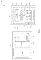
- FIG. 1is a diagram of a display system according to an exemplary embodiment of the present invention.
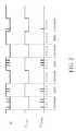
- FIG. 2is a timing diagram illustrating a control signal, a clock signal and a process signal, respectively.
- FIG. 1is a diagram of a display system 100 according to an exemplary embodiment of the present invention.
- the display system 100includes, but is not limited to, a display device 110 , a panel 120 , a driving circuit 130 , a control circuit 140 , a flexible printed circuit 150 , and a charge pump circuit 160 .
- the panel 120is disposed on the display device 110 .
- the driving circuit 130is disposed on the display device 110 for driving the panel 120 .
- the control circuit 140is also disposed on the display device 110 and coupled to the driving circuit 130 , for generating a control signal SC to control the charge pump circuit 160 .
- the flexible printed circuit 150is externally coupled to the display device 110 .
- the charge pump circuit 160is disposed on the flexible printed circuit 150 for generating at least an output voltage to the driving circuit 130 according to the control signal SC generated by the control circuit 140 .
- the charge pump circuit 160includes a control pin 162 , a charge pump unit 164 , a separating circuit 166 and a processing unit 168 .
- the control pin 162is coupled to the control circuit 140 for receiving the control signal SC generated from the control circuit 140 .
- the charge pump unit 164is used for generating at least the output voltage to the driving circuit 130 .
- the separating circuit 166is coupled to the control pin 162 , for deriving a clock signal S clock and a process signal S process from the received control signal SC, wherein the process signal S process can be a data signal S data or a command signal S command .
- the processing unit 168is coupled between the separating circuit 166 and the charge pump unit 164 , for receiving the clock signal S clock and the process signal S process generated from the separating circuit 166 and controlling the charge pump unit 164 according to the clock signal S clock and the process signal S process .
- the charge pump circuit 160sets a pumping factor PF 1 and generates two output voltages VSP and VSN according to the control signal SC, wherein the output voltages VSP and VSN are transmitted to the driving circuit 130 for usage.
- the separating circuit 166 in this embodimentincludes a low pass filter 1662 and a high pass filter 1664 .
- the low pass filter 1662is coupled to the control pin 162 , for filtering the control signal SC to generate the clock signal S clock .
- the high pass filter 1664is coupled to the control pin 162 , for filtering the control signal SC to generate the process signal S process .
- the separating circuit 166utilizes two filters to derive the clock signal S clock and the process signal S process from the control signal SC, but this should not be taken as a limitation of the present invention. In other words, the separating circuit 166 can derive the clock signal S clock and the process signal S process by utilizing other kinds of circuits, depending upon the actual design considerations. Operations of the control circuit 140 and the charge pump circuit 160 will be detailed using certain figures and embodiments.
- FIG. 2is a timing diagram illustrating a control signal SC, a clock signal S clock and a process signal S process , respectively.
- the control circuit 140generates the control signal SC to control the charge pump circuit 160 according to the requirements of the driving circuit 130 .
- the control circuit 140combines the process signal S process transmitted with a high frequency and the clock signal S clock transmitted with a related low frequency into the control signal SC as shown in FIG. 2 .
- the present inventionis not limited thereto.
- the separating circuit 166 of the charge pump circuit 160receives the control signal SC via the control pin 162 .
- the low pass filter 1662 and the high pass filter 1664filter the received control signal SC to generate the clock signal S clock and the process signal S process shown in FIG. 2 , respectively.
- the high pass filter 1664 of the separating circuit 166selectively generates the data signals S data or the command signals S command according to a carrier position of a high-frequency signal component of the control signal SC.
- the high-frequency signal component of the control signal SC positioned at the high frequency of the clock signal S clockis regarded as the data signal S data (e.g., the logic value “0110” shown in FIG.
- the high-frequency signal component of the control signal SC positioned at the low frequency of the clock signal S clockis regarded as the command signal S command (e.g., the logic value “1011” shown in FIG. 2 ).
- the charge pump circuit 160can set the pumping factor PF 1 and generate the two output voltages VSP and VSN according to the clock signal S clock and the process signal S process . For example, in this embodiment, the charge pump circuit 160 sets the pumping factor PF 1 to 3/2 according to the command signal S command with logic value “1011”.
- the charge pump circuit 160is disposed on the flexible printed circuit 150 , rather than being disposed in the driving circuit 130 of the display device 110 . Therefore, the voltage converting efficiency of the charge pump circuit 160 can be substantially improved due to its not being limited by the indium tin oxide (ITO) resistors R. Furthermore, only one control signal SC is needed to control the voltage converting ratio of the charge pump circuit 160 , which minimizes the pin number (pin count) of the charge pump circuit 160 to achieve a goal of lowering cost.
- the abovementioned display device 110can be a TFT-LCD device and the driving circuit 130 can be a TFT-LCD driver IC, but this should not be construed as a limitation of the present invention.
- all of the devices implemented in the charge pump circuit 160can be integrated in a single IC (e.g., System-on-a-chip, SoC), therefore, the charge pump unit 164 can supply an output voltage more precisely.
- the present inventionprovides a display system disposing a charge pump circuit on an FPC externally coupled to its display device for improving its voltage converting efficiency.
- the display system of the present inventionutilizes a single control pin and a control signal to control the charge pump circuit disposed on the FPC. Therefore, the voltage converting efficiency of the charge pump circuit in this display system will not be limited by the indium tin oxide (ITO) resistors.
- ITOindium tin oxide
Landscapes
- Engineering & Computer Science (AREA)
- Chemical & Material Sciences (AREA)
- Crystallography & Structural Chemistry (AREA)
- Physics & Mathematics (AREA)
- Computer Hardware Design (AREA)
- General Physics & Mathematics (AREA)
- Theoretical Computer Science (AREA)
- Liquid Crystal Display Device Control (AREA)
- Control Of Indicators Other Than Cathode Ray Tubes (AREA)
Abstract
Description
Claims (8)
Priority Applications (3)
| Application Number | Priority Date | Filing Date | Title |
|---|---|---|---|
| US12/719,873US8525818B2 (en) | 2008-10-29 | 2010-03-09 | Display system |
| JP2010206542AJP5707072B2 (en) | 2010-03-09 | 2010-09-15 | Display system |
| CN 201010572520CN102194425B (en) | 2010-03-09 | 2010-12-01 | Display system |
Applications Claiming Priority (3)
| Application Number | Priority Date | Filing Date | Title |
|---|---|---|---|
| US10919308P | 2008-10-29 | 2008-10-29 | |
| US12/370,585US8194060B2 (en) | 2008-10-29 | 2009-02-12 | Display system |
| US12/719,873US8525818B2 (en) | 2008-10-29 | 2010-03-09 | Display system |
Related Parent Applications (1)
| Application Number | Title | Priority Date | Filing Date |
|---|---|---|---|
| US12/370,585Continuation-In-PartUS8194060B2 (en) | 2008-10-29 | 2009-02-12 | Display system |
Publications (2)
| Publication Number | Publication Date |
|---|---|
| US20100164944A1 US20100164944A1 (en) | 2010-07-01 |
| US8525818B2true US8525818B2 (en) | 2013-09-03 |
Family
ID=42284345
Family Applications (1)
| Application Number | Title | Priority Date | Filing Date |
|---|---|---|---|
| US12/719,873Expired - Fee RelatedUS8525818B2 (en) | 2008-10-29 | 2010-03-09 | Display system |
Country Status (1)
| Country | Link |
|---|---|
| US (1) | US8525818B2 (en) |
Citations (21)
| Publication number | Priority date | Publication date | Assignee | Title |
|---|---|---|---|---|
| US20030011586A1 (en) | 2000-12-06 | 2003-01-16 | Yoshiharu Nakajima | Source voltage conversion circuit and its control method, display, and portable terminal |
| CN1410813A (en) | 2001-10-02 | 2003-04-16 | 株式会社日立制作所 | Liquid crystal display |
| TW200424995A (en) | 2003-05-07 | 2004-11-16 | Toshiba Matsushita Display Tec | El display device and its driving method |
| JP2004343893A (en) | 2003-05-15 | 2004-12-02 | Seiko Epson Corp | Boost circuit |
| US6862015B2 (en) | 2000-05-18 | 2005-03-01 | Hitachi, Ltd. | Liquid crystal display device |
| US20050099374A1 (en)* | 2003-10-01 | 2005-05-12 | Seiko Epson Corporation | Liquid crystal display device and liquid crystal panel |
| CN1664887A (en) | 2004-03-03 | 2005-09-07 | 精工爱普生株式会社 | Voltage supply circuit and method, power supply circuit, electro-optical device and electronic device |
| US20060012585A1 (en)* | 2002-11-25 | 2006-01-19 | Franciscus Schoofs | Multi output dc/dc converter for liquid crystal display device |
| US7110274B1 (en) | 2001-04-10 | 2006-09-19 | Renesas Technology Corp. | Semiconductor integrated circuit with voltage generation circuit, liquid crystal display controller and mobile electric equipment |
| US7167154B2 (en) | 2002-01-08 | 2007-01-23 | Hitachi, Ltd. | Display device |
| US20070024564A1 (en) | 2005-07-26 | 2007-02-01 | Koji Shimizu | Electro-optical device, method of driving electro-optical device, and electronic apparatus |
| US7212182B2 (en)* | 2002-06-05 | 2007-05-01 | Au Optronics Corporation | Drive circuit of TFTLCD |
| US20070132678A1 (en)* | 2005-06-14 | 2007-06-14 | Wei-Hsin Wei | Dimming method and system thereof |
| JP2007233202A (en) | 2006-03-02 | 2007-09-13 | Sharp Corp | Liquid crystal display |
| US20070229447A1 (en)* | 2006-03-23 | 2007-10-04 | Toshiba Matsushita Display Technology Co., Ltd. | Liquid crystal display device |
| CN101064467A (en) | 2006-04-27 | 2007-10-31 | 罗姆股份有限公司 | Power supply device, led driver, illumination device, and display device |
| US20080036752A1 (en)* | 1997-04-14 | 2008-02-14 | Diab Mohamed K | Signal processing apparatus and method |
| CN101136586A (en) | 2006-08-31 | 2008-03-05 | 圆创科技股份有限公司 | Multi-mode charge pump drive circuit for improving input noise during mode change |
| US20080084410A1 (en) | 2006-10-10 | 2008-04-10 | Seiko Epson Corporation | Power supply circuit, driver circuit, electro-optical device, electronic instrument, and common electrode drive method |
| TW200826052A (en) | 2006-08-31 | 2008-06-16 | Semiconductor Energy Lab | Liquid crystal display device |
| TW200837708A (en) | 2006-12-05 | 2008-09-16 | Semiconductor Energy Lab | Liquid crystal display device and driving method thereof |
- 2010
- 2010-03-09USUS12/719,873patent/US8525818B2/ennot_activeExpired - Fee Related
Patent Citations (22)
| Publication number | Priority date | Publication date | Assignee | Title |
|---|---|---|---|---|
| US20080036752A1 (en)* | 1997-04-14 | 2008-02-14 | Diab Mohamed K | Signal processing apparatus and method |
| US6862015B2 (en) | 2000-05-18 | 2005-03-01 | Hitachi, Ltd. | Liquid crystal display device |
| CN1419733A (en) | 2000-12-06 | 2003-05-21 | 索尼公司 | Conversion circuit and control method thereof, display and portable terminal |
| US20030011586A1 (en) | 2000-12-06 | 2003-01-16 | Yoshiharu Nakajima | Source voltage conversion circuit and its control method, display, and portable terminal |
| US7110274B1 (en) | 2001-04-10 | 2006-09-19 | Renesas Technology Corp. | Semiconductor integrated circuit with voltage generation circuit, liquid crystal display controller and mobile electric equipment |
| CN1410813A (en) | 2001-10-02 | 2003-04-16 | 株式会社日立制作所 | Liquid crystal display |
| US7167154B2 (en) | 2002-01-08 | 2007-01-23 | Hitachi, Ltd. | Display device |
| US7212182B2 (en)* | 2002-06-05 | 2007-05-01 | Au Optronics Corporation | Drive circuit of TFTLCD |
| US20060012585A1 (en)* | 2002-11-25 | 2006-01-19 | Franciscus Schoofs | Multi output dc/dc converter for liquid crystal display device |
| TW200424995A (en) | 2003-05-07 | 2004-11-16 | Toshiba Matsushita Display Tec | El display device and its driving method |
| JP2004343893A (en) | 2003-05-15 | 2004-12-02 | Seiko Epson Corp | Boost circuit |
| US20050099374A1 (en)* | 2003-10-01 | 2005-05-12 | Seiko Epson Corporation | Liquid crystal display device and liquid crystal panel |
| CN1664887A (en) | 2004-03-03 | 2005-09-07 | 精工爱普生株式会社 | Voltage supply circuit and method, power supply circuit, electro-optical device and electronic device |
| US20070132678A1 (en)* | 2005-06-14 | 2007-06-14 | Wei-Hsin Wei | Dimming method and system thereof |
| US20070024564A1 (en) | 2005-07-26 | 2007-02-01 | Koji Shimizu | Electro-optical device, method of driving electro-optical device, and electronic apparatus |
| JP2007233202A (en) | 2006-03-02 | 2007-09-13 | Sharp Corp | Liquid crystal display |
| US20070229447A1 (en)* | 2006-03-23 | 2007-10-04 | Toshiba Matsushita Display Technology Co., Ltd. | Liquid crystal display device |
| CN101064467A (en) | 2006-04-27 | 2007-10-31 | 罗姆股份有限公司 | Power supply device, led driver, illumination device, and display device |
| CN101136586A (en) | 2006-08-31 | 2008-03-05 | 圆创科技股份有限公司 | Multi-mode charge pump drive circuit for improving input noise during mode change |
| TW200826052A (en) | 2006-08-31 | 2008-06-16 | Semiconductor Energy Lab | Liquid crystal display device |
| US20080084410A1 (en) | 2006-10-10 | 2008-04-10 | Seiko Epson Corporation | Power supply circuit, driver circuit, electro-optical device, electronic instrument, and common electrode drive method |
| TW200837708A (en) | 2006-12-05 | 2008-09-16 | Semiconductor Energy Lab | Liquid crystal display device and driving method thereof |
Non-Patent Citations (5)
| Title |
|---|
| 1.5×/2× High-Efficiency White LED Charge Pumps, MAX1910/MAX1912 datasheet Rev 2, 2004 Maxim Integrated Products, MAXIM, Mar. 2004, pp. 1-11. |
| Dragan Maksimovic et al., "Switched-Capacitor DC-DC Converters for Low-Power On-Chip Applications", 1999 IEEE, Aug. 6, 1999, vol. 1, pp. 54-59. |
| Dragan Maksimović et al., "Switched-Capacitor DC-DC Converters for Low-Power On-Chip Applications", 1999 IEEE, Aug. 6, 1999, vol. 1, pp. 54-59. |
| Switched-Capacitor voltage Doublers, MAX1682/MAX1683 datasheet Rev 2, 2000 Maxim Integrated Products, MAXIM, Sep. 2000, pp. 1-8. |
| Switched-Capacitor voltage Inverters, MAX828/MAX829 datasheet Rev 3, 1999 Maxim Integrated Products, MAXIM, Sep. 1999, pp. 1-8. |
Also Published As
| Publication number | Publication date |
|---|---|
| US20100164944A1 (en) | 2010-07-01 |
Similar Documents
| Publication | Publication Date | Title |
|---|---|---|
| US10380965B2 (en) | Power circuit of displaying device | |
| CN203721167U (en) | Drive circuit of display panel, its drive module and display device | |
| CN103927995B (en) | Drive module with shared control end | |
| CN1453762A (en) | Efficient liquid crystal display drive voltage generating circuit and its method | |
| CN101950520B (en) | Level shifter, method for generating clock output signal and flat display device thereof | |
| US20010030571A1 (en) | Charge pump type power supply circuit and driving circuit for display device and display device using such power supply circuit | |
| JP7500780B2 (en) | Gate integrated driving circuit, display panel and display device | |
| US20110102069A1 (en) | Charge pump circuit and driving method thereof | |
| US8482551B2 (en) | Display system | |
| US20090002306A1 (en) | Common voltage generating circuit having square wave generating unit and liquid crystal display using same | |
| US8194060B2 (en) | Display system | |
| JP7617956B2 (en) | Display panel control circuit and display device | |
| CN1993876B (en) | Apparatus comprising a charge pump and LCD driver comprising such an apparatus | |
| US6650310B2 (en) | Low-power column driving method for liquid crystal display | |
| US8525818B2 (en) | Display system | |
| JP4269700B2 (en) | Display device | |
| TWI505616B (en) | Display system | |
| WO2014121474A1 (en) | Liquid crystal display and compensation circuit thereof, and shutdown method for voltage of thin-film transistor | |
| CN102194425B (en) | Display system | |
| CN101577097A (en) | Liquid crystal display device module and voltage generating circuit thereof | |
| CN102361399B (en) | Power supply device of thin film transistor liquid crystal display | |
| CN114882818B (en) | An ultra-low power open-loop LCD driver circuit based on an off-chip capacitor linear charge pump | |
| CN120148435B (en) | GOA driving circuit and display panel | |
| CN107845371B (en) | Power management integrated circuit and liquid crystal panel | |
| CN111211676B (en) | A display power isolation circuit with correct power-on and power-off timing sequence |
Legal Events
| Date | Code | Title | Description |
|---|---|---|---|
| AS | Assignment | Owner name:HIMAX TECHNOLOGIES LIMITED,TAIWAN Free format text:ASSIGNMENT OF ASSIGNORS INTEREST;ASSIGNORS:YANG, SSU-CHIEH;CHANG, YAW-GUANG;HUANG, HSIEN-TING;REEL/FRAME:024047/0373 Effective date:20100201 Owner name:HIMAX TECHNOLOGIES LIMITED, TAIWAN Free format text:ASSIGNMENT OF ASSIGNORS INTEREST;ASSIGNORS:YANG, SSU-CHIEH;CHANG, YAW-GUANG;HUANG, HSIEN-TING;REEL/FRAME:024047/0373 Effective date:20100201 | |
| STCF | Information on status: patent grant | Free format text:PATENTED CASE | |
| FPAY | Fee payment | Year of fee payment:4 | |
| FEPP | Fee payment procedure | Free format text:MAINTENANCE FEE REMINDER MAILED (ORIGINAL EVENT CODE: REM.); ENTITY STATUS OF PATENT OWNER: LARGE ENTITY | |
| LAPS | Lapse for failure to pay maintenance fees | Free format text:PATENT EXPIRED FOR FAILURE TO PAY MAINTENANCE FEES (ORIGINAL EVENT CODE: EXP.); ENTITY STATUS OF PATENT OWNER: LARGE ENTITY | |
| STCH | Information on status: patent discontinuation | Free format text:PATENT EXPIRED DUE TO NONPAYMENT OF MAINTENANCE FEES UNDER 37 CFR 1.362 | |
| FP | Lapsed due to failure to pay maintenance fee | Effective date:20210903 |