US8525354B2 - Bond pad structure and fabricating method thereof - Google Patents
Bond pad structure and fabricating method thereofDownload PDFInfo
- Publication number
- US8525354B2 US8525354B2US13/272,289US201113272289AUS8525354B2US 8525354 B2US8525354 B2US 8525354B2US 201113272289 AUS201113272289 AUS 201113272289AUS 8525354 B2US8525354 B2US 8525354B2
- Authority
- US
- United States
- Prior art keywords
- opening
- layer
- metal pad
- isolation layer
- metal
- Prior art date
- Legal status (The legal status is an assumption and is not a legal conclusion. Google has not performed a legal analysis and makes no representation as to the accuracy of the status listed.)
- Active, expires
Links
- 238000000034methodMethods0.000titleclaimsdescription41
- 229910052751metalInorganic materials0.000claimsabstractdescription81
- 239000002184metalSubstances0.000claimsabstractdescription81
- 238000002955isolationMethods0.000claimsabstractdescription66
- 239000010410layerSubstances0.000claimsdescription155
- 238000002161passivationMethods0.000claimsdescription19
- VYPSYNLAJGMNEJ-UHFFFAOYSA-NSilicium dioxideChemical compoundO=[Si]=OVYPSYNLAJGMNEJ-UHFFFAOYSA-N0.000claimsdescription17
- 229910052814silicon oxideInorganic materials0.000claimsdescription17
- 239000000758substrateSubstances0.000claimsdescription16
- 229910044991metal oxideInorganic materials0.000claimsdescription10
- 150000004706metal oxidesChemical class0.000claimsdescription10
- TWNQGVIAIRXVLR-UHFFFAOYSA-Noxo(oxoalumanyloxy)alumaneChemical compoundO=[Al]O[Al]=OTWNQGVIAIRXVLR-UHFFFAOYSA-N0.000claimsdescription10
- 229910052581Si3N4Inorganic materials0.000claimsdescription9
- HQVNEWCFYHHQES-UHFFFAOYSA-Nsilicon nitrideChemical compoundN12[Si]34N5[Si]62N3[Si]51N64HQVNEWCFYHHQES-UHFFFAOYSA-N0.000claimsdescription9
- 230000015572biosynthetic processEffects0.000claimsdescription8
- 239000000463materialSubstances0.000claimsdescription7
- 229910021417amorphous siliconInorganic materials0.000claimsdescription6
- 229920000620organic polymerPolymers0.000claimsdescription6
- 238000005452bendingMethods0.000claimsdescription5
- XUIMIQQOPSSXEZ-UHFFFAOYSA-NSiliconChemical compound[Si]XUIMIQQOPSSXEZ-UHFFFAOYSA-N0.000claimsdescription4
- 229910052782aluminiumInorganic materials0.000claimsdescription4
- XAGFODPZIPBFFR-UHFFFAOYSA-NaluminiumChemical group[Al]XAGFODPZIPBFFR-UHFFFAOYSA-N0.000claimsdescription4
- 229910052710siliconInorganic materials0.000claimsdescription4
- 239000010703siliconSubstances0.000claimsdescription4
- 239000011229interlayerSubstances0.000claimsdescription3
- 238000000059patterningMethods0.000claims2
- 230000008569processEffects0.000description25
- 238000004519manufacturing processMethods0.000description17
- 238000005530etchingMethods0.000description14
- KRHYYFGTRYWZRS-UHFFFAOYSA-NFluoraneChemical compoundFKRHYYFGTRYWZRS-UHFFFAOYSA-N0.000description3
- 239000004065semiconductorSubstances0.000description3
- 239000010409thin filmSubstances0.000description2
- 239000003153chemical reaction reagentSubstances0.000description1
- 230000000295complement effectEffects0.000description1
- 238000000151depositionMethods0.000description1
- 238000005137deposition processMethods0.000description1
- 238000005516engineering processMethods0.000description1
- 230000006872improvementEffects0.000description1
- 238000009413insulationMethods0.000description1
- 230000004048modificationEffects0.000description1
- 238000012986modificationMethods0.000description1
- QPJSUIGXIBEQAC-UHFFFAOYSA-Nn-(2,4-dichloro-5-propan-2-yloxyphenyl)acetamideChemical compoundCC(C)OC1=CC(NC(C)=O)=C(Cl)C=C1ClQPJSUIGXIBEQAC-UHFFFAOYSA-N0.000description1
- 230000003647oxidationEffects0.000description1
- 238000007254oxidation reactionMethods0.000description1
- 230000002093peripheral effectEffects0.000description1
- 239000002356single layerSubstances0.000description1
- 229910000679solderInorganic materials0.000description1
- 238000004528spin coatingMethods0.000description1
Images


Classifications
- H—ELECTRICITY
- H01—ELECTRIC ELEMENTS
- H01L—SEMICONDUCTOR DEVICES NOT COVERED BY CLASS H10
- H01L23/00—Details of semiconductor or other solid state devices
- H01L23/28—Encapsulations, e.g. encapsulating layers, coatings, e.g. for protection
- H01L23/31—Encapsulations, e.g. encapsulating layers, coatings, e.g. for protection characterised by the arrangement or shape
- H01L23/3157—Partial encapsulation or coating
- H01L23/3192—Multilayer coating
- B—PERFORMING OPERATIONS; TRANSPORTING
- B81—MICROSTRUCTURAL TECHNOLOGY
- B81B—MICROSTRUCTURAL DEVICES OR SYSTEMS, e.g. MICROMECHANICAL DEVICES
- B81B7/00—Microstructural systems; Auxiliary parts of microstructural devices or systems
- B81B7/0006—Interconnects
- H—ELECTRICITY
- H01—ELECTRIC ELEMENTS
- H01L—SEMICONDUCTOR DEVICES NOT COVERED BY CLASS H10
- H01L23/00—Details of semiconductor or other solid state devices
- H01L23/28—Encapsulations, e.g. encapsulating layers, coatings, e.g. for protection
- H01L23/29—Encapsulations, e.g. encapsulating layers, coatings, e.g. for protection characterised by the material, e.g. carbon
- H01L23/291—Oxides or nitrides or carbides, e.g. ceramics, glass
- H—ELECTRICITY
- H01—ELECTRIC ELEMENTS
- H01L—SEMICONDUCTOR DEVICES NOT COVERED BY CLASS H10
- H01L23/00—Details of semiconductor or other solid state devices
- H01L23/28—Encapsulations, e.g. encapsulating layers, coatings, e.g. for protection
- H01L23/29—Encapsulations, e.g. encapsulating layers, coatings, e.g. for protection characterised by the material, e.g. carbon
- H01L23/293—Organic, e.g. plastic
- B—PERFORMING OPERATIONS; TRANSPORTING
- B81—MICROSTRUCTURAL TECHNOLOGY
- B81B—MICROSTRUCTURAL DEVICES OR SYSTEMS, e.g. MICROMECHANICAL DEVICES
- B81B2207/00—Microstructural systems or auxiliary parts thereof
- B81B2207/01—Microstructural systems or auxiliary parts thereof comprising a micromechanical device connected to control or processing electronics, i.e. Smart-MEMS
- B81B2207/015—Microstructural systems or auxiliary parts thereof comprising a micromechanical device connected to control or processing electronics, i.e. Smart-MEMS the micromechanical device and the control or processing electronics being integrated on the same substrate
- H—ELECTRICITY
- H01—ELECTRIC ELEMENTS
- H01L—SEMICONDUCTOR DEVICES NOT COVERED BY CLASS H10
- H01L2224/00—Indexing scheme for arrangements for connecting or disconnecting semiconductor or solid-state bodies and methods related thereto as covered by H01L24/00
- H01L2224/01—Means for bonding being attached to, or being formed on, the surface to be connected, e.g. chip-to-package, die-attach, "first-level" interconnects; Manufacturing methods related thereto
- H01L2224/02—Bonding areas; Manufacturing methods related thereto
- H01L2224/04—Structure, shape, material or disposition of the bonding areas prior to the connecting process
- H01L2224/0401—Bonding areas specifically adapted for bump connectors, e.g. under bump metallisation [UBM]
- H—ELECTRICITY
- H01—ELECTRIC ELEMENTS
- H01L—SEMICONDUCTOR DEVICES NOT COVERED BY CLASS H10
- H01L2224/00—Indexing scheme for arrangements for connecting or disconnecting semiconductor or solid-state bodies and methods related thereto as covered by H01L24/00
- H01L2224/01—Means for bonding being attached to, or being formed on, the surface to be connected, e.g. chip-to-package, die-attach, "first-level" interconnects; Manufacturing methods related thereto
- H01L2224/02—Bonding areas; Manufacturing methods related thereto
- H01L2224/04—Structure, shape, material or disposition of the bonding areas prior to the connecting process
- H01L2224/04042—Bonding areas specifically adapted for wire connectors, e.g. wirebond pads
- H—ELECTRICITY
- H01—ELECTRIC ELEMENTS
- H01L—SEMICONDUCTOR DEVICES NOT COVERED BY CLASS H10
- H01L2224/00—Indexing scheme for arrangements for connecting or disconnecting semiconductor or solid-state bodies and methods related thereto as covered by H01L24/00
- H01L2224/01—Means for bonding being attached to, or being formed on, the surface to be connected, e.g. chip-to-package, die-attach, "first-level" interconnects; Manufacturing methods related thereto
- H01L2224/02—Bonding areas; Manufacturing methods related thereto
- H01L2224/04—Structure, shape, material or disposition of the bonding areas prior to the connecting process
- H01L2224/04073—Bonding areas specifically adapted for connectors of different types
- H—ELECTRICITY
- H01—ELECTRIC ELEMENTS
- H01L—SEMICONDUCTOR DEVICES NOT COVERED BY CLASS H10
- H01L2224/00—Indexing scheme for arrangements for connecting or disconnecting semiconductor or solid-state bodies and methods related thereto as covered by H01L24/00
- H01L2224/01—Means for bonding being attached to, or being formed on, the surface to be connected, e.g. chip-to-package, die-attach, "first-level" interconnects; Manufacturing methods related thereto
- H01L2224/02—Bonding areas; Manufacturing methods related thereto
- H01L2224/04—Structure, shape, material or disposition of the bonding areas prior to the connecting process
- H01L2224/05—Structure, shape, material or disposition of the bonding areas prior to the connecting process of an individual bonding area
- H01L2224/0554—External layer
- H01L2224/0556—Disposition
- H01L2224/05567—Disposition the external layer being at least partially embedded in the surface
- H—ELECTRICITY
- H01—ELECTRIC ELEMENTS
- H01L—SEMICONDUCTOR DEVICES NOT COVERED BY CLASS H10
- H01L2224/00—Indexing scheme for arrangements for connecting or disconnecting semiconductor or solid-state bodies and methods related thereto as covered by H01L24/00
- H01L2224/01—Means for bonding being attached to, or being formed on, the surface to be connected, e.g. chip-to-package, die-attach, "first-level" interconnects; Manufacturing methods related thereto
- H01L2224/02—Bonding areas; Manufacturing methods related thereto
- H01L2224/04—Structure, shape, material or disposition of the bonding areas prior to the connecting process
- H01L2224/05—Structure, shape, material or disposition of the bonding areas prior to the connecting process of an individual bonding area
- H01L2224/0554—External layer
- H01L2224/05599—Material
- H01L2224/056—Material with a principal constituent of the material being a metal or a metalloid, e.g. boron [B], silicon [Si], germanium [Ge], arsenic [As], antimony [Sb], tellurium [Te] and polonium [Po], and alloys thereof
- H01L2224/05617—Material with a principal constituent of the material being a metal or a metalloid, e.g. boron [B], silicon [Si], germanium [Ge], arsenic [As], antimony [Sb], tellurium [Te] and polonium [Po], and alloys thereof the principal constituent melting at a temperature of greater than or equal to 400°C and less than 950°C
- H01L2224/05624—Aluminium [Al] as principal constituent
- H—ELECTRICITY
- H01—ELECTRIC ELEMENTS
- H01L—SEMICONDUCTOR DEVICES NOT COVERED BY CLASS H10
- H01L24/00—Arrangements for connecting or disconnecting semiconductor or solid-state bodies; Methods or apparatus related thereto
- H01L24/01—Means for bonding being attached to, or being formed on, the surface to be connected, e.g. chip-to-package, die-attach, "first-level" interconnects; Manufacturing methods related thereto
- H01L24/02—Bonding areas ; Manufacturing methods related thereto
- H01L24/04—Structure, shape, material or disposition of the bonding areas prior to the connecting process
- H01L24/05—Structure, shape, material or disposition of the bonding areas prior to the connecting process of an individual bonding area
- H—ELECTRICITY
- H01—ELECTRIC ELEMENTS
- H01L—SEMICONDUCTOR DEVICES NOT COVERED BY CLASS H10
- H01L2924/00—Indexing scheme for arrangements or methods for connecting or disconnecting semiconductor or solid-state bodies as covered by H01L24/00
- H01L2924/10—Details of semiconductor or other solid state devices to be connected
- H01L2924/146—Mixed devices
- H01L2924/1461—MEMS
Definitions
- the present inventionrelates to a semiconductor device and the fabricating method thereof and more particularly relates to a bond pad structure and the fabricating method thereof.
- MEMSmicro-electro-mechanical systems
- a typical MEMS deviceis formed by a semiconductor process, wherein a plurality of micro-electromechanical elements are directly minimized and formed on a wafer, so as to be integrated with a circuit used for receiving, treating or transmitting signals resulted form the micro-electromechanical elements by at least one bond pads or bonding wires.
- the plurality of the MEMS devices formed on the wafershould be divided by a die sawing process.
- both of the MEMS devices and the bond pads of these micro-electromechanical elementsgenerally need to be exposed form the wafer surface via an opening, thus undercuts may occur on the sidewalls of the openings used to expose the bond pad of these micro-electromechanical elements due to the etching process subsequently performed to form the openings for exposing the MEMS devices. Accordingly, the bond pads may be damage by the impact of the die sawing process or the subsequent manufacturing procedurals, and at the worst case, material peeling may even occur.
- a bond pad structurecomprising an interconnection structure and an isolation layer.
- the interconnection structurehas at least one opening and at least one metal pad.
- the isolation layeris disposed on the interconnection structure and extends into the opening until in contact with the metal pad, whereby the sidewalls of the opening is blanketed by the isolation layer, and a portion of the metal pad is exposed from the opening.
- the isolation layeris made of a material selected from a group consisting of aluminum oxide (Al 2 O 3 ), silicon nitride (SiN), silicon carbonitride (SiCN), amorphous silicon, organic polymer and the arbitrary combinations thereof.
- the isolation layerhas a bending angle formed on the corner where the sidewalls of the opening adjoin to the metal pad.
- the interconnection structurecomprises an inter-layer dielectric (ILD) and a passivation layer, wherein the ILD is used to carry the metal pad, the passivation layer is disposed on the ILD, and the opening penetrates through the passivation layer to expose a portion of the metal pad.
- ILDinter-layer dielectric
- the bond pad structurefurther comprises a hard mask layer formed on the isolation layer without in contact with the metal pad.
- the hard mask layeris an aluminum layer.
- the bond pad structurefurther comprises a silicon oxide layer embedded between the hard mask layer and the isolation layer.
- the bond pad structurefurther comprises a metal oxide layer formed on the surface of the metal pad and disposed at the same side of the opening but not being exposed from the opening.
- a MEMS devicecomprising a substrate, a transistor, a micro-electromechanical element and a bond pad structure, wherein the transistor, the micro-electromechanical element and the bond pad structure are formed on the substrate.
- the bond pad structurecomprises an interconnection structure and an isolation layer.
- the interconnection structureis formed on the substrate and has at least one opening and at least one metal pad.
- the metal pad disposed in the dielectric layeris electrically connected to the transistor and the micro-electromechanical element.
- the isolation layeris disposed on the dielectric layer and extends into the opening until in contact with the metal pad, whereby the sidewalls of the opening is blanketed by the isolation layer, and a portion of the metal pad is exposed from the opening.
- the MEMS devicefurther comprises a hard mask layer formed on the isolation layer without in contact with the metal pad.
- the isolation layerhas a bending angle formed on a corner where the sidewalls of the opening adjoin to the metal pad.
- the MEMS devicefurther comprises a silicon oxide layer embedded between the hard mask layer and the isolation layer.
- the MEMS devicefurther comprises a metal oxide layer formed on the surface of the metal pad and disposed at the same side of the opening but not being exposed from the opening.
- a method for fabricating a bond pad structurecomprises steps as follows: An interconnection structure including an ILD and at least one metal pad is firstly provided. An opening is then formed on the ILD, so as to expose a portion of the metal pad. An isolation layer is subsequently formed on the ILD to cover the sidewalls of the opening and the exposed metal pad. Next, the isolation layer is patterned to expose a portion of the metal pad from the opening.
- the formation of the interconnection structurecomprises the following steps: Firstly, a substrate is provided, and then pluralities of patterned metal layers and an ILD used to isolate the patterned metal layers are formed on the substrate. A passivation layer is subsequently formed over the patterned metal layers and the ILD.
- the methodfurther comprises steps of forming at least one transistor and a portion of a micro-electromechanical element, prior to the formation of the interconnection structure.
- the methodfurther comprises steps of forming a metal oxide layer on the metal pad, before the passivation layer is formed.
- the isolation layeris made of a material selected from a group consisting of Al 2 O 3 , SiN, SiCN, amorphous silicon, organic polymer and the arbitrary combinations thereof.
- the methodfurther comprises steps of forming a hard mask layer on the isolation layer without in contact with the metal pad.
- the methodfurther comprises steps of forming a silicon oxide layer on the isolation layer without beyond the opening prior to the formation of the hard mask.
- a bond pad structure and the method for fabricating thereofare provided. Wherein an opening is defined on an interconnection structure to expose a portion of a metal pad. An isolation layer is then formed to cover the sidewalls of the opening and the exposed metal pad. The isolation layer is subsequently patterned to exposed the metal pad from the opening again, whereby the sidewalls of the opening are thoroughly covered by the patterned isolation layer.
- the isolation layerhas better etching resistance in comparison with the ILD layer of the interconnection structure, when the sidewalls of the opening are thoroughly covered by the isolation layer, it is more likely to prevent undercuts occurring in the interconnection structure and avoid the bond pad structure from being damaged due to the impacts of the subsequent manufacturing procedurals. Besides, since facilitating the bond pad structure can reduce the use of reticles in the subsequent manufacturing procedurals, thus the fabrication process can be simplified, the manufacturing cost should be significantly reduced and the objects of the present invention can be reached.
- the isolation layeris subsequently patterned so as to expose the portion of the metal pad form the opening again.
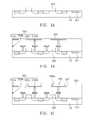
- FIGS. 1A to 1Eare cross sectional views illustrating the process for manufacturing a MEMS device, in accordance with one embodiment of the present invention.
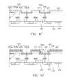
- FIGS. 1 C′ to 1 E′are cross sectional views illustrating a portion of the process for manufacturing a MEMS device, in accordance with another embodiment of the present invention.
- FIGS. 1A to 1Eare cross sectional views illustrating the process for manufacturing a MEMS device 100 , in accordance with one embodiment of the present invention.
- the MEMS device 100may be a micro-acoustical sensor, a gyro-sensor, an accelerometer or a clock generation and oscillator.
- the process for fabricating the MEMS device 100comprises steps as follows: Firstly, a substrate 101 having at least one micro-electromechanical element 104 and an electrical device used for receiving, dealing with or transmitting signals generated by the micro-electromechanical element 104 is provided (see FIG. 1A ).
- the substrate 101is a silicon substrate and preferably is a silicon wafer.
- the electrical device formed on the substrate 101comprises at least one complementary metal-oxide-semiconductor (CMOS) transistor 102 .
- CMOScomplementary metal-oxide-semiconductor
- the interconnection structure 103comprises a plurality of stacked metal layers, such as the patterned metal layers 103 a and 103 b , an ILD 103 c and at least one via contact 103 d , wherein the ILD 103 c is used to isolate the patterned metal layers 103 a and 103 b , and the via contact 103 d is used to electrically connect the patterned metal layers 103 a and 103 b.
- the patterned metal layers 103 a and 103 bpreferably are constituted by a plurality of pattered aluminum layers used to electrically connect to the micro-electromechanical element 104 and the CMOS transistor 102 , wherein a portion of the top patterned metal layers 103 a may serve as a metal pad (thereafter referred as metal pad 107 , for purpose of clearly description) used to be electrically connected to an external device via a bonding wire or a solder ball (not shown).
- a passivation layer 105is formed to cover the ILD 103 c and the metal pad 107 .
- the passivation layer 105preferably is made of silicon nitride.
- An etching processis then performed to remove a portion of the passivation layer 105 , whereby an opening 106 is formed in the passivation layer 105 so as to expose a portion of the metal pad 107 (see FIG. 1C ).
- an Al 2 O 3 thin filmmay be formed on the metal pad 107 by a deposition process or a thermal process (such as a thermal oxidation process), prior to the formation of the passivation layer 105 . And a portion of the Al 2 O 3 thin film can be removed by the aforementioned etching process to form a patterned metal oxide layer 112 after the passivation layer 105 is formed.
- the patterned metal oxide layer 112is formed on a surface of the metal pad 107 and disposed at the same side of the opening 106 but not being exposed from the opening 106 .
- an isolation layer 108 and a hard mask layer 110are sequentially formed on the passivation layer 105 and the exposed portion of the metal pad 107 .
- the portion of the isolation layer 108 extending into the opening 106blankets over the sidewalls 106 a of the opening 106 and bends to form a bending angle ⁇ on the corner where the sidewalls 106 a of the opening 106 adjoin the metal pad 107 .
- the preferred material used to form the isolation layer 108may be selected from a group consisting of Al 2 O 3 , SiN, SiCN, amorphous silicon, organic polymer and the arbitrary combinations thereof.
- the isolation layer 108may be a single layer or multiple stacked layers formed by depositing Al 2 O 3 , SiN, SiCN or amorphous silicon on the passivation layer 105 and the exposed portion of the metal pad 107 or formed by a spin coating process to separate organic polymer thereon.
- the hard mask layer 110preferably may be an aluminum layer.
- a second etching processis subsequently performed to remove portions of the hard mask layer 110 and the isolation layer 108 , such that a portion of the metal pad can be exposed from the opening 106 again. Wherein, the pattern hard mask layer 110 is not in contact with the metal pad 107 directly.
- At least one etching processsuch as an anisotropy etching process, is performed to form a MEMS opening 113 in the ILD 103 c , whereby the micro-electromechanical element 104 is exposed, and meanwhile the MEMS device 100 shown in FIG. 1E can be formed.
- a patterned silicon oxide layer 111may be provided to embedded between the isolation layer 108 and the hard mask layer 110 .
- the formation of the patterned silicon oxide layer 111comprises steps as follows: A silicon oxide layer 111 is firstly formed on the isolation layer 108 prior to the formation of the hard mask layer 110 (see FIG. 1 D′). A pattern process is then performed to pattern the silicon oxide layer 111 and make the patterned silicon oxide layer 111 without extending beyond the opening 106 .
- the hard mask layer 110is subsequently formed on the isolation layer 108 , the exposed metal pad 107 and the patterned silicon oxide layer 111 . Therefore, after the second etching process is carried out, the pattered silicon oxide layer 111 can be still thoroughly wrapped by the isolation layer 108 and the hard mask layer 110 .
- At least one etching processis performed to form a MEMS opening 113 in the ILD 103 c , whereby the micro-electromechanical element 104 is exposed, and meanwhile the MEMS device 100 ′ shown in FIG. 1 E′ is completed.
- the MEMS device 100 ′comprises an electrical device (the CMOS transistor 102 ), a micro-electromechanical element 104 and a bond pad structure.
- the bond pad structurecomprises an interconnection structure 103 (at least comprising an ILD 103 c , a metal pad 107 and a passivation layer 105 ), a patterned silicon oxide layer 111 , a metal oxide layer 112 , an isolation layer 108 and a hard mask layer 110 .
- the interconnection structure 103has an opening 106 .
- the metal pad 107 disposed in the dielectric layeris electrically connect to the CMOS transistor 102 and the micro-electromechanical element 104 .
- the isolation layer 108is disposed on the dielectric layer and extends into the opening 106 to cover the sidewalls 106 a of the opening 106 until in contact with the metal pad 107 , whereby a portion of the metal pad 107 can be exposed from the opening 106 .
- the hard mask layer 110is disposed on the isolation layer 108 without in contact to the metal pad 107 .
- the patterned silicon oxide layer 111is embedded between the isolation layer 108 and the hard mask layer 110 .
- the metal oxide layer 112is disposed on the surface of the metal pad 107 and disposed at the same side of the opening 106 but not being exposed from the opening 106 .
- the isolation layer 108 and the hard mask layer 110have an insulativity substantially the same as that of the ILD 103 c and have a better resistance against etching reagents, such as hydrofluoric acid (HF), in comparison with the ILD 103 c , thus the sidewalls 106 a of the opening 106 which are thoroughly covered by the isolation layer 108 and the hard mask layer 110 can be prevented from being damaged by the second etching process. Therefore, the impact of the die sawing process or the subsequent manufacturing procedurals may not conversely affect the bond pad structure to cause material peeling.
- etching reagentssuch as hydrofluoric acid (HF)
- a bond pad structure and the method for fabricating thereofare provided. Wherein an opening is defined on an interconnection structure to expose a portion of a metal pad. An isolation layer is then formed to cover the sidewalls of the opening and the exposed metal pad. The isolation layer is subsequently patterned to exposed the metal pad from the opening again, whereby the sidewalls of the opening are thoroughly covered by the patterned isolation layer.
- the isolation layerhas better etching resistance in comparison with the ILD layer of the interconnection structure, when the sidewalls of the opening are thoroughly covered by the isolation layer, it is more likely to prevent undercut occurring in interconnection structure and avoid the bond pad structure from being damaged due to the impacts of the subsequent manufacturing procedurals. Besides, since facilitating the bond pad structure can reduce the use of reticles in the subsequent manufacturing procedurals, thus the fabrication process can be simplified, the manufacturing cost should be significantly reduced and the objects of the present invention can be reached.
Landscapes
- Engineering & Computer Science (AREA)
- Computer Hardware Design (AREA)
- Microelectronics & Electronic Packaging (AREA)
- Physics & Mathematics (AREA)
- Condensed Matter Physics & Semiconductors (AREA)
- General Physics & Mathematics (AREA)
- Power Engineering (AREA)
- Chemical & Material Sciences (AREA)
- Ceramic Engineering (AREA)
- Internal Circuitry In Semiconductor Integrated Circuit Devices (AREA)
Abstract
Description
Claims (16)
Priority Applications (1)
| Application Number | Priority Date | Filing Date | Title |
|---|---|---|---|
| US13/272,289US8525354B2 (en) | 2011-10-13 | 2011-10-13 | Bond pad structure and fabricating method thereof |
Applications Claiming Priority (1)
| Application Number | Priority Date | Filing Date | Title |
|---|---|---|---|
| US13/272,289US8525354B2 (en) | 2011-10-13 | 2011-10-13 | Bond pad structure and fabricating method thereof |
Publications (2)
| Publication Number | Publication Date |
|---|---|
| US20130093104A1 US20130093104A1 (en) | 2013-04-18 |
| US8525354B2true US8525354B2 (en) | 2013-09-03 |
Family
ID=48085457
Family Applications (1)
| Application Number | Title | Priority Date | Filing Date |
|---|---|---|---|
| US13/272,289Active2032-01-25US8525354B2 (en) | 2011-10-13 | 2011-10-13 | Bond pad structure and fabricating method thereof |
Country Status (1)
| Country | Link |
|---|---|
| US (1) | US8525354B2 (en) |
Cited By (6)
| Publication number | Priority date | Publication date | Assignee | Title |
|---|---|---|---|---|
| CN104037077A (en)* | 2014-06-27 | 2014-09-10 | 宜特科技(昆山)电子有限公司 | Method for etching semiconductor chip |
| US20140264948A1 (en)* | 2013-03-15 | 2014-09-18 | Taiwan Semiconductor Manufacturing Company, Ltd. | Air Trench in Packages Incorporating Hybrid Bonding |
| US20150185247A1 (en)* | 2013-12-27 | 2015-07-02 | Feras Eid | Magnet placement for integrated sensor packages |
| US9178041B2 (en) | 2012-06-01 | 2015-11-03 | Taiwan Semiconductor Manufacturing Company, Ltd. | Power MOSFET and methods for forming the same |
| US9412844B2 (en) | 2012-06-01 | 2016-08-09 | Taiwan Semiconductor Manufacturing Company, Ltd. | Trench power MOSFET |
| US9624092B1 (en) | 2016-01-29 | 2017-04-18 | United Microelectronics Corp. | Semiconductor structure with micro-electro-mechanical system devices |
Families Citing this family (12)
| Publication number | Priority date | Publication date | Assignee | Title |
|---|---|---|---|---|
| US9349690B2 (en) | 2014-03-13 | 2016-05-24 | Taiwan Semiconductor Manufacturing Company Limited | Semiconductor arrangement and formation thereof |
| US9786633B2 (en)* | 2014-04-23 | 2017-10-10 | Massachusetts Institute Of Technology | Interconnect structures for fine pitch assembly of semiconductor structures and related techniques |
| KR102243492B1 (en)* | 2014-07-21 | 2021-04-23 | 삼성전자주식회사 | Semiconductor device and method for manufacturing the same |
| WO2016025451A1 (en) | 2014-08-11 | 2016-02-18 | Massachusetts Institute Of Technology | Interconnect structures for assembly of multi-layer semiconductor devices |
| WO2016118210A2 (en) | 2014-11-05 | 2016-07-28 | Massachusetts Institute Of Technology | Interconnect structures for assembly of multi-layer semiconductor devices |
| US10134972B2 (en) | 2015-07-23 | 2018-11-20 | Massachusetts Institute Of Technology | Qubit and coupler circuit structures and coupling techniques |
| WO2017015432A1 (en) | 2015-07-23 | 2017-01-26 | Massachusetts Institute Of Technology | Superconducting integrated circuit |
| US10242968B2 (en) | 2015-11-05 | 2019-03-26 | Massachusetts Institute Of Technology | Interconnect structure and semiconductor structures for assembly of cryogenic electronic packages |
| WO2017079417A1 (en) | 2015-11-05 | 2017-05-11 | Massachusetts Institute Of Technology | Interconnect structures for assembly of semiconductor structures including superconducting integrated circuits |
| US10381541B2 (en) | 2016-10-11 | 2019-08-13 | Massachusetts Institute Of Technology | Cryogenic electronic packages and methods for fabricating cryogenic electronic packages |
| US10392246B2 (en) | 2016-12-30 | 2019-08-27 | Texas Instruments Incorporated | Through-substrate conductor support |
| US10892239B1 (en)* | 2019-07-10 | 2021-01-12 | Globalfoundries Singapore Pte. Ltd. | Bond pad reliability of semiconductor devices |
Citations (62)
| Publication number | Priority date | Publication date | Assignee | Title |
|---|---|---|---|---|
| US5136364A (en)* | 1991-06-12 | 1992-08-04 | National Semiconductor Corporation | Semiconductor die sealing |
| US5523595A (en)* | 1990-08-21 | 1996-06-04 | Ramtron International Corporation | Semiconductor device having a transistor, a ferroelectric capacitor and a hydrogen barrier film |
| US5573679A (en) | 1995-06-19 | 1996-11-12 | Alberta Microelectronic Centre | Fabrication of a surface micromachined capacitive microphone using a dry-etch process |
| US5719073A (en) | 1993-02-04 | 1998-02-17 | Cornell Research Foundation, Inc. | Microstructures and single mask, single-crystal process for fabrication thereof |
| US6243474B1 (en) | 1996-04-18 | 2001-06-05 | California Institute Of Technology | Thin film electret microphone |
| US6265328B1 (en) | 1998-01-30 | 2001-07-24 | Silicon Genesis Corporation | Wafer edge engineering method and device |
| US20010023086A1 (en) | 1999-12-28 | 2001-09-20 | Ki-Nam Park | Method for reducing dark current in image sensor |
| US6635509B1 (en) | 2002-04-12 | 2003-10-21 | Dalsa Semiconductor Inc. | Wafer-level MEMS packaging |
| US6725719B2 (en) | 2002-04-17 | 2004-04-27 | Milli Sensor Systems And Actuators, Inc. | MEMS-integrated inertial measurement units on a common substrate |
| US20040122328A1 (en) | 2000-06-19 | 2004-06-24 | University Of Washington | Integrated optical scanning image acquisition and display |
| US6829131B1 (en) | 1999-09-13 | 2004-12-07 | Carnegie Mellon University | MEMS digital-to-acoustic transducer with error cancellation |
| US6841848B2 (en) | 2003-06-06 | 2005-01-11 | Analog Devices, Inc. | Composite semiconductor wafer and a method for forming the composite semiconductor wafer |
| US20050014317A1 (en) | 2003-07-18 | 2005-01-20 | Pyo Sung Gyu | Method for forming inductor in semiconductor device |
| US6872902B2 (en) | 2000-11-29 | 2005-03-29 | Microassembly Technologies, Inc. | MEMS device with integral packaging |
| US20050076719A1 (en) | 2003-10-10 | 2005-04-14 | Henrik Jakobsen | Capacitive sensor |
| US6887391B1 (en) | 2000-03-24 | 2005-05-03 | Analog Devices, Inc. | Fabrication and controlled release of structures using etch-stop trenches |
| US20050162806A1 (en) | 2004-01-22 | 2005-07-28 | Zyvex Corporation | Thermal plastic deformation of RF MEMS devices |
| US6936524B2 (en) | 2003-11-05 | 2005-08-30 | Akustica, Inc. | Ultrathin form factor MEMS microphones and microspeakers |
| US20050194688A1 (en)* | 2001-03-28 | 2005-09-08 | Yehiel Gotkis | Semiconductor structure implementing low-k dielectric materials and supporting stubs |
| US6943448B2 (en) | 2003-01-23 | 2005-09-13 | Akustica, Inc. | Multi-metal layer MEMS structure and process for making the same |
| US6946728B2 (en) | 2004-02-19 | 2005-09-20 | Hewlett-Packard Development Company, L.P. | System and methods for hermetic sealing of post media-filled MEMS package |
| US20050221529A1 (en) | 2001-12-06 | 2005-10-06 | Microfabrica Inc. | Complex microdevices and apparatus and methods for fabricating such devices |
| US7045459B2 (en) | 2002-02-19 | 2006-05-16 | Northrop Grumman Corporation | Thin film encapsulation of MEMS devices |
| US7049051B2 (en) | 2003-01-23 | 2006-05-23 | Akustica, Inc. | Process for forming and acoustically connecting structures on a substrate |
| US20060223329A1 (en) | 2005-04-05 | 2006-10-05 | Analog Devices, Inc. | Vapor HF etch process mask and method |
| US7129172B2 (en) | 2004-03-29 | 2006-10-31 | Intel Corporation | Bonded wafer processing method |
| US20060260401A1 (en) | 2003-02-24 | 2006-11-23 | Huikai Xie | Integrated monolithic tri-axial micromachined accelerometer |
| US7152474B2 (en) | 2002-09-18 | 2006-12-26 | Carnegie Mellon University | Built-in self test of MEMS |
| US20070003082A1 (en) | 2001-11-27 | 2007-01-04 | Corporation For National Research Initiatives | Miniature condenser microphone and fabrication method therefor |
| US20070007858A1 (en) | 2003-05-15 | 2007-01-11 | Oticon A/S | Microphone with adjustable properties |
| US20070023851A1 (en) | 2002-04-23 | 2007-02-01 | Hartzell John W | MEMS pixel sensor |
| US20070040270A1 (en) | 2003-10-10 | 2007-02-22 | Koninklijke Philips Electronics N.V. | Electronic device and carrier substrate |
| US20070047900A1 (en) | 2005-07-22 | 2007-03-01 | Sampsell Jeffrey B | MEMS devices having support structures and methods of fabricating the same |
| US20070054205A1 (en) | 2005-09-08 | 2007-03-08 | Wen-Kuang Lin | Process for forming anti-reflection coating and method for improving accuracy of overlay measurement and alignment |
| US20070125161A1 (en) | 2005-12-01 | 2007-06-07 | Janusz Bryzek | Integrated tire pressure sensor system |
| US7242569B2 (en) | 2002-10-18 | 2007-07-10 | Ngimat, Co. | Tunable capacitors using fluid dielectrics |
| US20070187793A1 (en) | 2006-02-13 | 2007-08-16 | Samsung Electronics Co., Ltd. | Filter, color filter array, method of manufacturing the color filter array, and image sensor |
| US7280436B2 (en) | 2004-05-07 | 2007-10-09 | Corporation For National Research Initiatives | Miniature acoustic detector based on electron surface tunneling |
| US7288424B2 (en) | 2002-05-28 | 2007-10-30 | Silicon Light Machines Corporation | Integrated driver process flow |
| US20070284682A1 (en) | 2006-03-20 | 2007-12-13 | Laming Richard I | Mems process and device |
| US7329933B2 (en) | 2004-10-29 | 2008-02-12 | Silicon Matrix Pte. Ltd. | Silicon microphone with softly constrained diaphragm |
| US20080094686A1 (en) | 2006-10-19 | 2008-04-24 | U Ren Gregory David | Sacrificial spacer process and resultant structure for MEMS support structure |
| US20080137884A1 (en) | 2006-12-06 | 2008-06-12 | Electronics And Telecommunications Research Institute | Condenser microphone having flexure hinge diaphragm and method of manufacturing the same |
| US20080163687A1 (en) | 2004-10-15 | 2008-07-10 | Morgan Research Corporation | MEMS Sensor Suite on a Chip |
| US20080304681A1 (en) | 2007-06-06 | 2008-12-11 | Analog Devices, Inc. | Microphone with Aligned Apertures |
| US20090134459A1 (en)* | 2007-11-16 | 2009-05-28 | Yasushi Goto | Semiconductor device and method of manufacturing the same |
| US20090180655A1 (en) | 2008-01-10 | 2009-07-16 | Lingsen Precision Industries, Ltd. | Package for mems microphone |
| US20090243004A1 (en) | 2008-03-27 | 2009-10-01 | Bang-Chiang Lan | Integrated structure for MEMS device and semiconductor device and method of fabricating the same |
| US20090302415A1 (en) | 2008-06-04 | 2009-12-10 | Karl-Heinz Mueller | Micro-Electromechanical System Devices |
| US20100002894A1 (en) | 2008-07-03 | 2010-01-07 | Bang-Chiang Lan | MEMS device and method of making the same |
| US20100052179A1 (en) | 2008-09-02 | 2010-03-04 | United Microelectronics Corp. | Mems structure and method for fabricating the same |
| US20100067728A1 (en) | 2008-09-16 | 2010-03-18 | United Microelectronics Corp. | Microelectromechanical system microphone structure and microelectromechanical system microphone package structure |
| US20100074458A1 (en) | 2008-09-19 | 2010-03-25 | United Microelectronics Corp. | Structure of mems electroacoustic transducer and fabricating method thereof |
| US20100084735A1 (en) | 2008-10-08 | 2010-04-08 | Chin-Sheng Yang | Semiconductor assembly and method for forming seal ring |
| US20100090298A1 (en) | 2008-10-09 | 2010-04-15 | United Microelectronics Corp. | Mems diaphragm |
| US20100144156A1 (en) | 2008-12-09 | 2010-06-10 | Hui-Shen Shih | Method to integrate micro electro mechanical system and cmos image sensor |
| US20100213568A1 (en) | 2009-02-24 | 2010-08-26 | PixArt Imaging Incorporation, R.O.C. | Micro-electro-mechanical-system device with guard ring and method for making same |
| US20100270628A1 (en) | 2009-04-26 | 2010-10-28 | Hui-Shen Shih | Multifunction mens element and integrated method for making mos and multifunction mens |
| US20110006350A1 (en) | 2008-12-14 | 2011-01-13 | Hui-Shen Shih | Integrated structure of mems device and cmos image sensor device |
| US20110012227A1 (en) | 2008-10-08 | 2011-01-20 | Chin-Sheng Yang | Semiconductor assembly |
| US20110031624A1 (en) | 2009-08-10 | 2011-02-10 | Bang-Chiang Lan | MEMS and a Protection Structure Thereof |
| US7939932B2 (en) | 2007-06-20 | 2011-05-10 | Analog Devices, Inc. | Packaged chip devices with atomic layer deposition protective films |
- 2011
- 2011-10-13USUS13/272,289patent/US8525354B2/enactiveActive
Patent Citations (65)
| Publication number | Priority date | Publication date | Assignee | Title |
|---|---|---|---|---|
| US5523595A (en)* | 1990-08-21 | 1996-06-04 | Ramtron International Corporation | Semiconductor device having a transistor, a ferroelectric capacitor and a hydrogen barrier film |
| US5136364A (en)* | 1991-06-12 | 1992-08-04 | National Semiconductor Corporation | Semiconductor die sealing |
| US5719073A (en) | 1993-02-04 | 1998-02-17 | Cornell Research Foundation, Inc. | Microstructures and single mask, single-crystal process for fabrication thereof |
| US5573679A (en) | 1995-06-19 | 1996-11-12 | Alberta Microelectronic Centre | Fabrication of a surface micromachined capacitive microphone using a dry-etch process |
| US6806593B2 (en) | 1996-04-18 | 2004-10-19 | California Institute Of Technology | Thin film electret microphone |
| US6243474B1 (en) | 1996-04-18 | 2001-06-05 | California Institute Of Technology | Thin film electret microphone |
| US6265328B1 (en) | 1998-01-30 | 2001-07-24 | Silicon Genesis Corporation | Wafer edge engineering method and device |
| US7019955B2 (en) | 1999-09-13 | 2006-03-28 | Carnegie Mellon University | MEMS digital-to-acoustic transducer with error cancellation |
| US6829131B1 (en) | 1999-09-13 | 2004-12-07 | Carnegie Mellon University | MEMS digital-to-acoustic transducer with error cancellation |
| US20010023086A1 (en) | 1999-12-28 | 2001-09-20 | Ki-Nam Park | Method for reducing dark current in image sensor |
| US6887391B1 (en) | 2000-03-24 | 2005-05-03 | Analog Devices, Inc. | Fabrication and controlled release of structures using etch-stop trenches |
| US20040122328A1 (en) | 2000-06-19 | 2004-06-24 | University Of Washington | Integrated optical scanning image acquisition and display |
| US6872902B2 (en) | 2000-11-29 | 2005-03-29 | Microassembly Technologies, Inc. | MEMS device with integral packaging |
| US20050194688A1 (en)* | 2001-03-28 | 2005-09-08 | Yehiel Gotkis | Semiconductor structure implementing low-k dielectric materials and supporting stubs |
| US20070003082A1 (en) | 2001-11-27 | 2007-01-04 | Corporation For National Research Initiatives | Miniature condenser microphone and fabrication method therefor |
| US20050221529A1 (en) | 2001-12-06 | 2005-10-06 | Microfabrica Inc. | Complex microdevices and apparatus and methods for fabricating such devices |
| US7045459B2 (en) | 2002-02-19 | 2006-05-16 | Northrop Grumman Corporation | Thin film encapsulation of MEMS devices |
| US6635509B1 (en) | 2002-04-12 | 2003-10-21 | Dalsa Semiconductor Inc. | Wafer-level MEMS packaging |
| US6725719B2 (en) | 2002-04-17 | 2004-04-27 | Milli Sensor Systems And Actuators, Inc. | MEMS-integrated inertial measurement units on a common substrate |
| US20070023851A1 (en) | 2002-04-23 | 2007-02-01 | Hartzell John W | MEMS pixel sensor |
| US7288424B2 (en) | 2002-05-28 | 2007-10-30 | Silicon Light Machines Corporation | Integrated driver process flow |
| US7152474B2 (en) | 2002-09-18 | 2006-12-26 | Carnegie Mellon University | Built-in self test of MEMS |
| US7242569B2 (en) | 2002-10-18 | 2007-07-10 | Ngimat, Co. | Tunable capacitors using fluid dielectrics |
| US6943448B2 (en) | 2003-01-23 | 2005-09-13 | Akustica, Inc. | Multi-metal layer MEMS structure and process for making the same |
| US7202101B2 (en) | 2003-01-23 | 2007-04-10 | Akustica, Inc. | Multi-metal layer MEMS structure and process for making the same |
| US7049051B2 (en) | 2003-01-23 | 2006-05-23 | Akustica, Inc. | Process for forming and acoustically connecting structures on a substrate |
| US20060260401A1 (en) | 2003-02-24 | 2006-11-23 | Huikai Xie | Integrated monolithic tri-axial micromachined accelerometer |
| US20070007858A1 (en) | 2003-05-15 | 2007-01-11 | Oticon A/S | Microphone with adjustable properties |
| US6841848B2 (en) | 2003-06-06 | 2005-01-11 | Analog Devices, Inc. | Composite semiconductor wafer and a method for forming the composite semiconductor wafer |
| US20050014317A1 (en) | 2003-07-18 | 2005-01-20 | Pyo Sung Gyu | Method for forming inductor in semiconductor device |
| US20050076719A1 (en) | 2003-10-10 | 2005-04-14 | Henrik Jakobsen | Capacitive sensor |
| US20070040270A1 (en) | 2003-10-10 | 2007-02-22 | Koninklijke Philips Electronics N.V. | Electronic device and carrier substrate |
| US6936524B2 (en) | 2003-11-05 | 2005-08-30 | Akustica, Inc. | Ultrathin form factor MEMS microphones and microspeakers |
| US20050162806A1 (en) | 2004-01-22 | 2005-07-28 | Zyvex Corporation | Thermal plastic deformation of RF MEMS devices |
| US6946728B2 (en) | 2004-02-19 | 2005-09-20 | Hewlett-Packard Development Company, L.P. | System and methods for hermetic sealing of post media-filled MEMS package |
| US7129172B2 (en) | 2004-03-29 | 2006-10-31 | Intel Corporation | Bonded wafer processing method |
| US7280436B2 (en) | 2004-05-07 | 2007-10-09 | Corporation For National Research Initiatives | Miniature acoustic detector based on electron surface tunneling |
| US20080163687A1 (en) | 2004-10-15 | 2008-07-10 | Morgan Research Corporation | MEMS Sensor Suite on a Chip |
| US7329933B2 (en) | 2004-10-29 | 2008-02-12 | Silicon Matrix Pte. Ltd. | Silicon microphone with softly constrained diaphragm |
| US20060223329A1 (en) | 2005-04-05 | 2006-10-05 | Analog Devices, Inc. | Vapor HF etch process mask and method |
| US20070047900A1 (en) | 2005-07-22 | 2007-03-01 | Sampsell Jeffrey B | MEMS devices having support structures and methods of fabricating the same |
| US20070054205A1 (en) | 2005-09-08 | 2007-03-08 | Wen-Kuang Lin | Process for forming anti-reflection coating and method for improving accuracy of overlay measurement and alignment |
| US20070125161A1 (en) | 2005-12-01 | 2007-06-07 | Janusz Bryzek | Integrated tire pressure sensor system |
| US20070187793A1 (en) | 2006-02-13 | 2007-08-16 | Samsung Electronics Co., Ltd. | Filter, color filter array, method of manufacturing the color filter array, and image sensor |
| US20070284682A1 (en) | 2006-03-20 | 2007-12-13 | Laming Richard I | Mems process and device |
| US20080094686A1 (en) | 2006-10-19 | 2008-04-24 | U Ren Gregory David | Sacrificial spacer process and resultant structure for MEMS support structure |
| US20080137884A1 (en) | 2006-12-06 | 2008-06-12 | Electronics And Telecommunications Research Institute | Condenser microphone having flexure hinge diaphragm and method of manufacturing the same |
| US20080304681A1 (en) | 2007-06-06 | 2008-12-11 | Analog Devices, Inc. | Microphone with Aligned Apertures |
| US7939932B2 (en) | 2007-06-20 | 2011-05-10 | Analog Devices, Inc. | Packaged chip devices with atomic layer deposition protective films |
| US20090134459A1 (en)* | 2007-11-16 | 2009-05-28 | Yasushi Goto | Semiconductor device and method of manufacturing the same |
| US20090180655A1 (en) | 2008-01-10 | 2009-07-16 | Lingsen Precision Industries, Ltd. | Package for mems microphone |
| US20090243004A1 (en) | 2008-03-27 | 2009-10-01 | Bang-Chiang Lan | Integrated structure for MEMS device and semiconductor device and method of fabricating the same |
| US20090302415A1 (en) | 2008-06-04 | 2009-12-10 | Karl-Heinz Mueller | Micro-Electromechanical System Devices |
| US20100002894A1 (en) | 2008-07-03 | 2010-01-07 | Bang-Chiang Lan | MEMS device and method of making the same |
| US20100052179A1 (en) | 2008-09-02 | 2010-03-04 | United Microelectronics Corp. | Mems structure and method for fabricating the same |
| US20100067728A1 (en) | 2008-09-16 | 2010-03-18 | United Microelectronics Corp. | Microelectromechanical system microphone structure and microelectromechanical system microphone package structure |
| US20100074458A1 (en) | 2008-09-19 | 2010-03-25 | United Microelectronics Corp. | Structure of mems electroacoustic transducer and fabricating method thereof |
| US20100084735A1 (en) | 2008-10-08 | 2010-04-08 | Chin-Sheng Yang | Semiconductor assembly and method for forming seal ring |
| US20110012227A1 (en) | 2008-10-08 | 2011-01-20 | Chin-Sheng Yang | Semiconductor assembly |
| US20100090298A1 (en) | 2008-10-09 | 2010-04-15 | United Microelectronics Corp. | Mems diaphragm |
| US20100144156A1 (en) | 2008-12-09 | 2010-06-10 | Hui-Shen Shih | Method to integrate micro electro mechanical system and cmos image sensor |
| US20110006350A1 (en) | 2008-12-14 | 2011-01-13 | Hui-Shen Shih | Integrated structure of mems device and cmos image sensor device |
| US20100213568A1 (en) | 2009-02-24 | 2010-08-26 | PixArt Imaging Incorporation, R.O.C. | Micro-electro-mechanical-system device with guard ring and method for making same |
| US20100270628A1 (en) | 2009-04-26 | 2010-10-28 | Hui-Shen Shih | Multifunction mens element and integrated method for making mos and multifunction mens |
| US20110031624A1 (en) | 2009-08-10 | 2011-02-10 | Bang-Chiang Lan | MEMS and a Protection Structure Thereof |
Cited By (14)
| Publication number | Priority date | Publication date | Assignee | Title |
|---|---|---|---|---|
| US9412844B2 (en) | 2012-06-01 | 2016-08-09 | Taiwan Semiconductor Manufacturing Company, Ltd. | Trench power MOSFET |
| US10510880B2 (en) | 2012-06-01 | 2019-12-17 | Taiwan Semiconductor Manufacturing Company, Ltd. | Trench power MOSFET |
| US10109732B2 (en) | 2012-06-01 | 2018-10-23 | Taiwan Semiconductor Manufacturing Company, Ltd. | Trench power MOSFET |
| US9178041B2 (en) | 2012-06-01 | 2015-11-03 | Taiwan Semiconductor Manufacturing Company, Ltd. | Power MOSFET and methods for forming the same |
| US9443796B2 (en)* | 2013-03-15 | 2016-09-13 | Taiwan Semiconductor Manufacturing Company, Ltd. | Air trench in packages incorporating hybrid bonding |
| US9312229B2 (en) | 2013-03-15 | 2016-04-12 | Taiwan Semiconductor Manufacturing Company, Ltd. | Hybrid bonding with air-gap structure |
| US9502396B2 (en) | 2013-03-15 | 2016-11-22 | Taiwan Semiconductor Manufacturing Company, Ltd. | Air trench in packages incorporating hybrid bonding |
| US9786628B2 (en) | 2013-03-15 | 2017-10-10 | Taiwan Semiconductor Manufacturing Company, Ltd. | Air trench in packages incorporating hybrid bonding |
| US9960142B2 (en) | 2013-03-15 | 2018-05-01 | Taiwan Semiconductor Manufacturing Company, Ltd. | Hybrid bonding with air-gap structure |
| US20140264948A1 (en)* | 2013-03-15 | 2014-09-18 | Taiwan Semiconductor Manufacturing Company, Ltd. | Air Trench in Packages Incorporating Hybrid Bonding |
| US9791470B2 (en)* | 2013-12-27 | 2017-10-17 | Intel Corporation | Magnet placement for integrated sensor packages |
| US20150185247A1 (en)* | 2013-12-27 | 2015-07-02 | Feras Eid | Magnet placement for integrated sensor packages |
| CN104037077A (en)* | 2014-06-27 | 2014-09-10 | 宜特科技(昆山)电子有限公司 | Method for etching semiconductor chip |
| US9624092B1 (en) | 2016-01-29 | 2017-04-18 | United Microelectronics Corp. | Semiconductor structure with micro-electro-mechanical system devices |
Also Published As
| Publication number | Publication date |
|---|---|
| US20130093104A1 (en) | 2013-04-18 |
Similar Documents
| Publication | Publication Date | Title |
|---|---|---|
| US8525354B2 (en) | Bond pad structure and fabricating method thereof | |
| JP4775007B2 (en) | Semiconductor device and manufacturing method thereof | |
| KR101918609B1 (en) | Integrated circuit device | |
| US8779605B2 (en) | Method and apparatus providing integrated circuit having redistribution layer with recessed connectors | |
| CN113345857B (en) | Semiconductor element and method for manufacturing the same | |
| US8810012B2 (en) | Chip package, method for forming the same, and package wafer | |
| TWI807087B (en) | Semiconductor device structure and method of forming the same | |
| US20170062387A1 (en) | Semiconductor chip, semiconductor package including the same, and method of fabricating the same | |
| US9059110B2 (en) | Reduction of fluorine contamination of bond pads of semiconductor devices | |
| US8173539B1 (en) | Method for fabricating metal redistribution layer | |
| US10256179B2 (en) | Package structure and manufacturing method thereof | |
| JP2012119444A (en) | Semiconductor device | |
| US8278754B2 (en) | Metal line in semiconductor device and method for forming the same | |
| KR20090022325A (en) | Bonding pad of semiconductor device and manufacturing method thereof | |
| TWI523145B (en) | Bond pad structure and fabricating method thereof | |
| US10793426B2 (en) | Microelectromechanical system structure and method for fabricating the same | |
| JP6937724B2 (en) | Semiconductor devices and their manufacturing methods | |
| KR100876885B1 (en) | Semiconductor package and manufacturing method thereof | |
| KR100855702B1 (en) | Wafer Level Package Manufacturing Method | |
| KR100835442B1 (en) | Pad structure of semiconductor device and manufacturing method thereof | |
| US8664114B2 (en) | Image sensor and method for fabricating the same | |
| US8772930B2 (en) | Increased surface area electrical contacts for microelectronic packages | |
| KR20120006771A (en) | Semiconductor package and manufacturing method thereof | |
| US20080188024A1 (en) | Method of fabricating micro mechanical moving member and metal interconnects thereof | |
| CN105845665A (en) | Semiconductor device and manufacturing method thereof, and electronic apparatus |
Legal Events
| Date | Code | Title | Description |
|---|---|---|---|
| AS | Assignment | Owner name:UNITED MICROELECTRONICS CORPORATION, TAIWAN Free format text:ASSIGNMENT OF ASSIGNORS INTEREST;ASSIGNORS:WU, HUI-MIN;WANG, MING-I;WANG, KUAN-YU;AND OTHERS;REEL/FRAME:027053/0700 Effective date:20111006 | |
| FEPP | Fee payment procedure | Free format text:PAYOR NUMBER ASSIGNED (ORIGINAL EVENT CODE: ASPN); ENTITY STATUS OF PATENT OWNER: LARGE ENTITY | |
| STCF | Information on status: patent grant | Free format text:PATENTED CASE | |
| FPAY | Fee payment | Year of fee payment:4 | |
| MAFP | Maintenance fee payment | Free format text:PAYMENT OF MAINTENANCE FEE, 8TH YEAR, LARGE ENTITY (ORIGINAL EVENT CODE: M1552); ENTITY STATUS OF PATENT OWNER: LARGE ENTITY Year of fee payment:8 | |
| AS | Assignment | Owner name:MARLIN SEMICONDUCTOR LIMITED, IRELAND Free format text:ASSIGNMENT OF ASSIGNORS INTEREST;ASSIGNOR:UNITED MICROELECTRONICS CORPORATION;REEL/FRAME:056991/0292 Effective date:20210618 | |
| MAFP | Maintenance fee payment | Free format text:PAYMENT OF MAINTENANCE FEE, 12TH YEAR, LARGE ENTITY (ORIGINAL EVENT CODE: M1553); ENTITY STATUS OF PATENT OWNER: LARGE ENTITY Year of fee payment:12 |